WO2022044524A1 - 弾性波フィルタ回路、マルチプレクサ、フロントエンド回路および通信装置 - Google Patents
弾性波フィルタ回路、マルチプレクサ、フロントエンド回路および通信装置 Download PDFInfo
- Publication number
- WO2022044524A1 WO2022044524A1 PCT/JP2021/024343 JP2021024343W WO2022044524A1 WO 2022044524 A1 WO2022044524 A1 WO 2022044524A1 JP 2021024343 W JP2021024343 W JP 2021024343W WO 2022044524 A1 WO2022044524 A1 WO 2022044524A1
- Authority
- WO
- WIPO (PCT)
- Prior art keywords
- band
- uplink
- operation band
- downlink
- filter circuit
- Prior art date
- Legal status (The legal status is an assumption and is not a legal conclusion. Google has not performed a legal analysis and makes no representation as to the accuracy of the status listed.)
- Ceased
Links
Images




Classifications
-
- H—ELECTRICITY
- H04—ELECTRIC COMMUNICATION TECHNIQUE
- H04B—TRANSMISSION
- H04B1/00—Details of transmission systems, not covered by a single one of groups H04B3/00 - H04B13/00; Details of transmission systems not characterised by the medium used for transmission
- H04B1/38—Transceivers, i.e. devices in which transmitter and receiver form a structural unit and in which at least one part is used for functions of transmitting and receiving
- H04B1/40—Circuits
- H04B1/50—Circuits using different frequencies for the two directions of communication
-
- H—ELECTRICITY
- H03—ELECTRONIC CIRCUITRY
- H03H—IMPEDANCE NETWORKS, e.g. RESONANT CIRCUITS; RESONATORS
- H03H9/00—Networks comprising electromechanical or electro-acoustic elements; Electromechanical resonators
- H03H9/46—Filters
- H03H9/64—Filters using surface acoustic waves
-
- H—ELECTRICITY
- H03—ELECTRONIC CIRCUITRY
- H03H—IMPEDANCE NETWORKS, e.g. RESONANT CIRCUITS; RESONATORS
- H03H9/00—Networks comprising electromechanical or electro-acoustic elements; Electromechanical resonators
- H03H9/70—Multiple-port networks for connecting several sources or loads, working on different frequencies or frequency bands, to a common load or source
- H03H9/72—Networks using surface acoustic waves
-
- H—ELECTRICITY
- H04—ELECTRIC COMMUNICATION TECHNIQUE
- H04B—TRANSMISSION
- H04B1/00—Details of transmission systems, not covered by a single one of groups H04B3/00 - H04B13/00; Details of transmission systems not characterised by the medium used for transmission
-
- H—ELECTRICITY
- H04—ELECTRIC COMMUNICATION TECHNIQUE
- H04B—TRANSMISSION
- H04B1/00—Details of transmission systems, not covered by a single one of groups H04B3/00 - H04B13/00; Details of transmission systems not characterised by the medium used for transmission
- H04B1/005—Details of transmission systems, not covered by a single one of groups H04B3/00 - H04B13/00; Details of transmission systems not characterised by the medium used for transmission adapting radio receivers, transmitters andtransceivers for operation on two or more bands, i.e. frequency ranges
- H04B1/0053—Details of transmission systems, not covered by a single one of groups H04B3/00 - H04B13/00; Details of transmission systems not characterised by the medium used for transmission adapting radio receivers, transmitters andtransceivers for operation on two or more bands, i.e. frequency ranges with common antenna for more than one band
- H04B1/0057—Details of transmission systems, not covered by a single one of groups H04B3/00 - H04B13/00; Details of transmission systems not characterised by the medium used for transmission adapting radio receivers, transmitters andtransceivers for operation on two or more bands, i.e. frequency ranges with common antenna for more than one band using diplexing or multiplexing filters for selecting the desired band
-
- H—ELECTRICITY
- H04—ELECTRIC COMMUNICATION TECHNIQUE
- H04B—TRANSMISSION
- H04B1/00—Details of transmission systems, not covered by a single one of groups H04B3/00 - H04B13/00; Details of transmission systems not characterised by the medium used for transmission
- H04B1/005—Details of transmission systems, not covered by a single one of groups H04B3/00 - H04B13/00; Details of transmission systems not characterised by the medium used for transmission adapting radio receivers, transmitters andtransceivers for operation on two or more bands, i.e. frequency ranges
- H04B1/0053—Details of transmission systems, not covered by a single one of groups H04B3/00 - H04B13/00; Details of transmission systems not characterised by the medium used for transmission adapting radio receivers, transmitters andtransceivers for operation on two or more bands, i.e. frequency ranges with common antenna for more than one band
- H04B1/006—Details of transmission systems, not covered by a single one of groups H04B3/00 - H04B13/00; Details of transmission systems not characterised by the medium used for transmission adapting radio receivers, transmitters andtransceivers for operation on two or more bands, i.e. frequency ranges with common antenna for more than one band using switches for selecting the desired band
-
- H—ELECTRICITY
- H03—ELECTRONIC CIRCUITRY
- H03H—IMPEDANCE NETWORKS, e.g. RESONANT CIRCUITS; RESONATORS
- H03H9/00—Networks comprising electromechanical or electro-acoustic elements; Electromechanical resonators
- H03H9/70—Multiple-port networks for connecting several sources or loads, working on different frequencies or frequency bands, to a common load or source
- H03H9/703—Networks using bulk acoustic wave devices
- H03H9/706—Duplexers
-
- H—ELECTRICITY
- H03—ELECTRONIC CIRCUITRY
- H03H—IMPEDANCE NETWORKS, e.g. RESONANT CIRCUITS; RESONATORS
- H03H9/00—Networks comprising electromechanical or electro-acoustic elements; Electromechanical resonators
- H03H9/70—Multiple-port networks for connecting several sources or loads, working on different frequencies or frequency bands, to a common load or source
- H03H9/72—Networks using surface acoustic waves
- H03H9/725—Duplexers
-
- H—ELECTRICITY
- H04—ELECTRIC COMMUNICATION TECHNIQUE
- H04B—TRANSMISSION
- H04B1/00—Details of transmission systems, not covered by a single one of groups H04B3/00 - H04B13/00; Details of transmission systems not characterised by the medium used for transmission
- H04B1/38—Transceivers, i.e. devices in which transmitter and receiver form a structural unit and in which at least one part is used for functions of transmitting and receiving
- H04B1/40—Circuits
- H04B1/54—Circuits using the same frequency for two directions of communication
Definitions
- the present invention relates to elastic wave filter circuits, multiplexers, front-end circuits and communication devices.
- Patent Document 1 discloses a receiving module (transmission circuit) having a configuration in which a plurality of filters having different pass bands are connected to an antenna via a multiplexer (switch).
- 3GPP 3rd Generation Partnership Project
- simultaneous transmission of a high frequency signal in the 5G (5th generation) -NR (New Radio) band and a high frequency signal in the 4G (4th generation) -LTE (Long term Evolution) band, etc. Is required.
- an object of the present invention is to provide a small elastic wave filter circuit, a multiplexer, a front-end circuit, and a communication device in which isolation between two bands having a small frequency gap is ensured.
- the elastic wave filter circuit has a first band for frequency division duplex (FDD) composed of a first downlink operation band and a first uplink operation band, and a second downlink operation.
- FDD frequency division duplex
- the second band for FDD composed of the band and the second uplink operation band, (1) the first downlink operation band, the second downlink operation band, and the first uplink operation from the low frequency side or the high frequency side.
- the band and the second uplink operation band, or (2) the first downlink operation band, the first uplink operation band, the second uplink operation band, and the second downlink operation band are located in this order.
- the first uplink operation band and the second uplink operation band do not overlap in frequency range and are formed on a single piece of piezoelectric first substrate, and the first uplink operation band and the second uplink operation band are formed. It has a pass band including a link operation band.
- the elastic wave filter circuit has a first band for time division duplex (TDD) composed of a first downlink operation band and a first uplink operation band, and a second downlink operation.
- TDD time division duplex
- the first downlink operation band and the first uplink operation band are in the same frequency range, and are from the low frequency side or the high frequency side.
- 1st band, 2nd uplink operation band, and 2nd downlink operation band, and the 1st band and the 2nd uplink operation band do not overlap in frequency range. It is formed on a single piezoelectric first substrate and has a pass-through band including a first uplink operating band and a second uplink operating band.
- the multiplexer is connected to the antenna connection terminal, the elastic wave filter circuit described above connected to the antenna connection terminal, and the antenna connection terminal, and has a first downlink operation band and a second down.
- a first filter circuit having a pass band including a link operation band is provided, and the first filter circuit is formed on a second substrate different from the first substrate.
- the multiplexer is connected to the antenna connection terminal, the elastic wave filter circuit described above connected to the antenna connection terminal, and the antenna connection terminal, and is connected to the first downlink operation band and the second down.
- a first filter circuit having a pass band including a link operation band, and an antenna constituting the elastic wave filter circuit are in contact with a first dielectric layer formed on the first substrate, and the first one is in contact with the first dielectric layer.
- the antenna constituting the filter circuit is in contact with a second dielectric layer formed on the first substrate, which is different from the first dielectric layer.
- the front-end circuit includes an antenna connection terminal, the elastic wave filter circuit described above connected to the antenna connection terminal, and a first band and a second band connected to the antenna connection terminal.
- a second filter circuit having a pass-through band including a third uplink operating band of the third band in which frequencies do not overlap, a power amplifier capable of amplifying high-frequency signals of the first band, the second band, and the third band, and an elastic wave.
- a switch that switches the connection between the filter circuit and the power amplifier and the connection between the second filter circuit and the power amplifier, and an impedance matching circuit that is connected between the power amplifier and the switch and changes the impedance in response to the switch change. , Equipped with.
- the communication device includes a signal processing circuit for processing a high frequency signal and the front-end circuit described above for transmitting a high frequency signal between the signal processing circuit and the antenna.
- the present invention it is possible to provide a small elastic wave filter circuit, a multiplexer, a front-end circuit and a communication device in which isolation between two bands having a small frequency gap is ensured.
- FIG. 1 is a circuit configuration diagram of a front-end circuit and a communication device according to an embodiment.
- FIG. 2 is a diagram showing the relationship of bands in the embodiment.
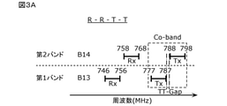
- FIG. 3A is a diagram showing a first example of a combination of bands in the embodiment.
- FIG. 3B is a diagram showing a second example of the combination of bands in the embodiment.
- FIG. 3C is a diagram showing a third example of a combination of bands in the embodiment.
- FIG. 3D is a diagram showing a fourth example of band combinations in the embodiment.
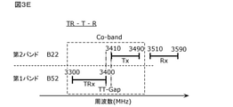
- FIG. 3E is a diagram showing a fifth example of band combinations in the embodiment.
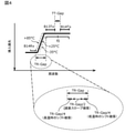
- FIG. 4 is a diagram showing required specifications of the frequency temperature coefficient of the elastic wave filter circuit according to the embodiment.
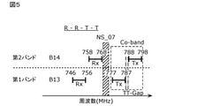
- FIG. 5 is a diagram showing the arrangement of NS-07 in the first example of the combination of bands in the embodiment.
- each figure is a schematic diagram in which emphasis, omission, or ratio is adjusted as appropriate to show the present invention, and is not necessarily exactly illustrated. What is the actual shape, positional relationship, and ratio? May be different. In each figure, substantially the same configuration is designated by the same reference numeral, and duplicate description may be omitted or simplified.
- connection means not only the case of being directly connected by a connection terminal and / or a wiring conductor, but also the case of being electrically connected via another circuit element.
- connected between A and B means being connected to A and B on the route connecting A and B.
- FIG. 1 is a circuit configuration diagram of a front-end circuit 1 and a communication device 5 according to the first embodiment.
- the communication device 5 includes a front-end circuit 1, an antenna 2, an RF signal processing circuit (RFIC) 3, and a baseband signal processing circuit (BBIC) 4. Be prepared.
- RFIC RF signal processing circuit
- BBIC baseband signal processing circuit
- the front-end circuit 1 transmits a high-frequency signal between the antenna 2 and the RFIC 3.
- the detailed circuit configuration of the front-end circuit 1 will be described later.
- the antenna 2 is connected to the antenna connection terminal 100 of the front-end circuit 1, transmits a high-frequency signal output from the front-end circuit 1, and also receives a high-frequency signal from the outside and outputs it to the front-end circuit 1.
- RFIC3 is an example of a signal processing circuit that processes high frequency signals. Specifically, the RFIC 3 processes a high-frequency reception signal input via the reception path of the front-end circuit 1 by down-conversion or the like, and outputs the reception signal generated by the signal processing to the BBIC 4. Further, the RFIC 3 processes the transmission signal input from the BBIC 4 by up-conversion or the like, and outputs the high frequency transmission signal generated by the signal processing to the transmission path of the front-end circuit 1. Further, the RFIC 3 has a control unit that controls a switch, an amplifier, and the like included in the front-end circuit 1. A part or all of the function of the RFIC3 as a control unit may be mounted outside the RFIC3, or may be mounted on, for example, the BBIC4 or the front-end circuit 1.
- the BBIC 4 is a baseband signal processing circuit that processes signals using an intermediate frequency band having a lower frequency than the high frequency signal transmitted by the front end circuit 1.
- the signal processed by the BBIC 4 for example, an image signal for displaying an image and / or an audio signal for a call via a speaker are used.
- the antenna 2 and the BBIC 4 are not essential components.
- the front-end circuit 1 includes filters 11, 12, 21 and 22, a power amplifier 51, a low noise amplifier 52, switches 30, 31 and 32, a matching circuit 41, and an antenna connection terminal. It includes 100, a high frequency input terminal 110, and a high frequency output terminal 120.
- the antenna connection terminal 100 is connected to the antenna 2.
- the high frequency input terminal 110 is a terminal for receiving a high frequency transmission signal from the outside of the front end circuit 1.
- the high frequency output terminal 120 is a terminal for providing a high frequency reception signal to the outside of the front end circuit 1.
- the power amplifier 51 can amplify high frequency transmission signals (hereinafter referred to as transmission signals) of the first band, the second band, and the third band input from the high frequency input terminal 110.
- the power amplifier 51 is connected between the high frequency input terminal 110 and the switch 31.
- the low noise amplifier 52 amplifies the high frequency reception signals (hereinafter referred to as reception signals) of the first band, the second band, and the third band input from the antenna connection terminal 100.
- the low noise amplifier 52 is connected between the high frequency output terminal 120 and the switch 32.
- each of the first band, the second band, and the third band is a standardization organization or the like (for example, 3GPP, IEEE (Institute of Electrical and Electronics Engineers)) for a communication system constructed by using radio access technology (RAT). Electrical and Electronics Engineers), etc.) means a frequency band defined in advance.
- RAT radio access technology
- the communication system for example, an LTE system, a 5G-NR system, a WLAN (Wireless Local Area Network) system, or the like can be used, but the communication system is not limited thereto.
- the first band is composed of a first downlink operation band and a first uplink operation band.
- the second band is composed of a second downlink operation band and a second uplink operation band.
- the third band is composed of a third downlink operation band and a third uplink operation band.
- the uplink operation band means the frequency range specified for the uplink among the above bands. Further, the downlink operation band means a frequency range designated for the downlink among the above bands.
- the first band is, for example, the band B13 for LTE for frequency division duplex (FDD), and the second band is, for example, for FDD.
- Band B14 for LTE Band B8 for LTE for FDD.
- the filter 11 is an example of an elastic wave filter circuit, and is a pass band including a first uplink operation band (first transmission band) of the first band and a second uplink operation band (second transmission band) of the second band. have.
- the filter 11 is connected to the antenna connection terminal 100 via the switch 30.
- the filter 11 is a surface acoustic wave filter or a surface acoustic wave filter using BAW (Bulk Acoustic Wave).
- the filter 12 is an example of a first filter circuit, and is a pass band including a first downlink operation band (first reception band) of the first band and a second downlink operation band (second reception band) of the second band. have.
- the filter 12 is connected to the antenna connection terminal 100 via the switch 30.
- the filter 21 is an example of the second filter circuit, and has a pass band including the third uplink operation band of the third band.
- the filter 21 is connected to the antenna connection terminal 100 via the switch 30.
- the filter 22 has a pass band including a third downlink operation band of the third band.
- the filter 22 is connected to the antenna connection terminal 100 via the switch 30.
- the filters 21 and 22 may form a duplexer that allows the transmission signal and the reception signal of the third band to pass through.
- the switch 30 has four SPST (Single Pole Single Throw) type switch elements. One terminal of each switch element is connected to the antenna connection terminal 100. The other terminal of each switch element is connected to a filter 11, 12, 21 or 22, respectively. With this configuration, the switch 30 switches between connection and non-connection between the antenna connection terminal 100 and the filter 11 and switches between connection and non-connection between the antenna connection terminal 100 and the filter 12 based on, for example, a control signal from RFIC 3. The connection and non-connection between the antenna connection terminal 100 and the filter 21 are switched, and the connection and non-connection between the antenna connection terminal 100 and the filter 22 are switched. The number of switch elements included in the switch 30 is appropriately set according to the number of filters included in the front-end circuit 1.
- the switch 31 is connected between the filters 11 and 21 and the power amplifier 51.
- the switch 31 has a common terminal and two selection terminals.
- the common terminal of the switch 31 is connected to the output terminal of the power amplifier 51 via the matching circuit 41.
- the two selection terminals of the switch 31 are connected to the filters 11 and 21, respectively.
- the switch 31 switches the connection between the filter 11 and the power amplifier 51 and the connection between the filter 21 and the power amplifier 51, for example, based on the control signal from the RFIC 3.
- the switch 32 is connected between the filters 12 and 22 and the low noise amplifier 52. Specifically, the switch 32 has a common terminal and two selection terminals. The common terminal of the switch 32 is connected to the input terminal of the low noise amplifier 52. The two selection terminals of the switch 32 are connected to the filters 12 and 22, respectively. With this connection configuration, the switch 32 switches the connection between the filter 12 and the low noise amplifier 52 and the connection between the filter 22 and the low noise amplifier 52, for example, based on the control signal from the RFIC 3.
- the matching circuit 41 is an example of an impedance matching circuit, which is connected between the power amplifier 51 and the switch 31 and changes the impedance in response to the switching of the switch 31.
- the switch 30 may not be provided, and each of the filters 11, 12, 21 and 22 may be directly connected to the antenna connection terminal 100.
- the filters 11 and 12 and the switch 30 constitute a multiplexer.
- the multiplexer may not have a switch 30, and the filters 11 and 12 may be directly connected to the antenna connection terminal 100.
- the front-end circuit 1 may include at least filters 11, 21, a power amplifier 51, a switch 31, and a matching circuit 41, and may not include other circuit elements.
- FIG. 2 is a diagram showing the relationship of bands in the embodiment.
- the first band is band B13 for LTE for FDD
- the first downlink operation band is 746-756 MHz
- the first uplink operation band is 777-787 MHz.
- the second band is band B14 for LTE for FDD
- the second downlink operating band is 758-768 MHz
- the second uplink operating band is 788-798 MHz.
- the third band is band B8 for LTE for FDD
- the third downlink operating band is 925-960 MHz
- the third uplink operating band is 880-915 MHz.
- the first downlink operation band, the second downlink operation band, the first uplink operation band, and the second uplink operation band in that order. It is located so that the first uplink operation band and the second uplink operation band do not overlap in frequency range. Further, there is a frequency gap (TT-Gap: 1 MHz) between the first uplink operation band and the second uplink operation band. Further, the frequency of the third band does not overlap with that of the first band and the second band.
- T-Gap 1 MHz
- the filter 11 is a (Co-band) filter having a pass band including a first uplink operation band of the first band and a second uplink operation band of the second band.
- FIG. 3A is a diagram showing a first example of a combination of bands in the embodiment.
- the figure shows an application example of the first band and the second band shown in FIG. That is, the first band is the band B13 for LTE for FDD, and the second band is the band B14 for LTE for FDD.
- the first band and the second band from the low frequency side, (1) the first downlink operation band (R), the second downlink operation band (R), the first uplink operation band (T), and the second. It is located in the order of the uplink operation band (T), (RRT-T), and there is a frequency gap (TT-Gap) between the first uplink operation band and the second uplink operation band. 1MHz) exists.
- the filter 11 is a (Co-band) filter having a pass band including an uplink operation band of band B13 and an uplink operation band of band B14.
- FIG. 3B is a diagram showing a second example of the combination of bands in the embodiment.
- the first band is band B13 for LTE for FDD
- the first downlink operating band is 746-756 MHz
- the first uplink operating band is 777-787 MHz.
- the second band is band B26 for LTE for FDD
- the second downlink operating band is 859-894 MHz
- the second uplink operating band is 814-849 MHz.
- the first band and the second band from the low frequency side, (1) the first downlink operation band (R), the first uplink operation band (T), the second uplink operation band (T), and the second.
- the filter 11 is a (Co-band) filter having a pass band including an uplink operation band of band B13 and an uplink operation band of band B26.
- FIG. 3C is a diagram showing a third example of a combination of bands in the embodiment.
- the first band is band B11 for LTE for FDD
- the first uplink operating band is 1427.9-1447.9 MHz
- the first downlink operating band is 1475.9-1495.9 MHz. ..
- the second band is band B21 for LTE for FDD
- the second uplink operating band is 1447.9-1462.9 MHz
- the second downlink operating band is 1495.9-1510.9 MHz. ..
- the downlink operation band (R) is located in the order (T-T-R-R), and the frequency ranges of the first uplink operation band and the second uplink operation band do not overlap.
- the frequency gap (TT-Gap) between the first uplink operation band and the second uplink operation band is 0 MHz.
- the filter 11 is a (Co-band) filter having a pass band including the uplink operation band of the band B11 and the uplink operation band of the band B21.
- FIG. 3D is a diagram showing a fourth example of a combination of bands in the embodiment.
- the first band is band B71 for LTE for FDD, the first uplink operating band is 663-698 MHz, and the first downlink operating band is 617-652 MHz.
- the second band is band B68 for LTE for FDD, the second uplink operating band is 698-728 MHz, and the second downlink operating band is 753-783 MHz.
- the first band and the second band from the low frequency side, (1) the first downlink operation band (R), the first uplink operation band (T), the second uplink operation band (T), and the second.
- the downlink operation band (R) is located in the order (RTT-R), and the frequency ranges of the first uplink operation band and the second uplink operation band do not overlap.
- the frequency gap (TT-Gap) between the first uplink operation band and the second uplink operation band is 0 MHz.
- the filter 11 is a (Co-band) filter having a pass band including an uplink operation band of band B71 and an uplink operation band of band B68.
- FIG. 3E is a diagram showing a fifth example of a combination of bands in the embodiment.
- the first band is band B52 for LTE for Time Division Duplex (TDD), and the first uplink operation band and the first downlink operation band have the same frequency range, and both are in the same frequency range. It is 3300-3400 MHz.
- the second band is band B22 for LTE for FDD, the second uplink operating band is 3410-3490 MHz, and the second downlink operating band is 3510-3590 MHz.
- the first band and the second band from the low frequency side, (1) the first band (the first downlink operation band and the first uplink operation band), the second uplink operation band (T), and the second down.
- the filter 11 is a (Co-band) filter having a pass band including the uplink operation band (and the downlink operation band) of the band B52 and the uplink operation band of the band B22.
- the bands for LTE are shown as the first and second bands of the first to fifth examples described above, but the first and second bands of the first to fifth examples are NR. It may be a band for.
- the filter 11 is an elastic wave filter formed on a single piezoelectric first substrate, and has a pass band including a first uplink operation band and a second uplink operation band.
- the first uplink operation band and the second uplink operation band do not sandwich the first downlink operation band and the second downlink operation band. , Adjacent to each other. Therefore, when the filter 11 is configured by a surface acoustic wave filter, it is possible to form a pass band including a first uplink operation band and a second uplink operation band by using a common IDT (Interdigital transducer) electrode. Will be. Further, since it is a surface acoustic wave filter, it is possible to steeply attenuate the downlink operation band adjacent to the pass band. Therefore, it is possible to realize a small elastic wave filter circuit that sufficiently attenuates adjacent downlink operation bands and uses two uplink operation bands as a common passband.
- IDT Interdigital transducer
- the filter 11 has a small frequency temperature coefficient TCF, and the frequency temperature coefficient TCF of the filter 11 is preferably 10 ppm / ° C. or less. According to this, even if the temperature of the filter 11 that passes the high output transmission signal rises, the frequency drift of the passing characteristic of the filter 11 can be suppressed. Therefore, it is possible to secure a large amount of attenuation of the downlink operation band of the filter 11.
- FIG. 4 is a diagram showing the required specifications of the frequency temperature coefficient TCF of the filter 11 in the embodiment. The figure shows an allowable amount when the passing characteristic of the filter 11 changes in frequency due to a temperature change.
- the attenuation amount on the lower frequency side than the pass band of the filter 11 there is a concern that the attenuation amount will deteriorate due to the shift of the pass band to the low frequency side at high temperature (+ 85 ° C).
- the amount of shift of the pass characteristic to the low frequency side is the first uplink operation band (B13Tx) of the band B13 constituting the low frequency side of the pass band of the filter 11 and the band B14 adjacent to the low frequency side thereof. It is desirable that the frequency gap is within 1/4 of the frequency gap TR-Gap with the second downlink operation band (B14Rx).
- the attenuation amount on the high frequency side of the pass band of the filter 11 there is a concern that the attenuation amount deteriorates due to the shift of the pass band to the high frequency side at low temperature (-35 ° C.).
- the amount of shift of the pass characteristic to the high frequency side is the frequency between the second uplink operation band (B14Tx) of the band B14 constituting the high frequency side of the pass band of the filter 11 and the attenuation band close to the high frequency side. It is desirable that the gap is within 1/4 of the TR-Gap.
- the center frequency of the pass band of the filter 11 is set to f0 (Hz), and the frequency between the first downlink operation band and the first downlink operation band or the second downlink operation band adjacent to the first downlink operation band.
- the gap is fgap (Hz) and the maximum temperature change width from room temperature (25 ° C.) is ⁇ T
- TCF ppm / ° C.
- the filter 11 a large amount of attenuation of the attenuation band on the low frequency side of the pass band at high temperature can be secured, and a large amount of attenuation of the attenuation band on the high frequency side of the pass band at low temperature can be secured.
- the required EVM Error Vector Magnitude
- TCF of the filter 11 so as to satisfy the equation 1, it is possible to reduce the EVM of the received signals of the first band and the second band.
- FIG. 5 is a diagram showing the arrangement of NS_07 in the first example of the combination of bands in the embodiment.
- NS_07 (769-775 MHz) between the second downlink operation band (758-768 MHz) and the first uplink operation band (777-787 MHz).
- the unnecessary radiation level in NS_07 must be equal to or less than a predetermined value.
- TCF of the filter 11 by setting the frequency temperature coefficient TCF of the filter 11 so as to satisfy the equation 1, the unnecessary radiation level in NS-07 can be set to a predetermined value or less.
- the front-end circuit 1 is connected to the antenna connection terminal 100, the filter 11 connected to the antenna connection terminal 100, and the antenna connection terminal 100, and has frequencies of the first band and the second band.
- a filter 21 having a pass band including a third uplink operating band of the third band that does not overlap, a power amplifier 51 capable of amplifying high frequency signals of the first band, the second band, and the third band, and a filter 11 and a power amplifier.
- a switch 31 that switches the connection between the filter 21 and the power amplifier 51 and a matching circuit 41 that is connected between the power amplifier 51 and the switch 31 and changes the impedance in response to the switching of the switch 31. To prepare for.
- the impedance of the matching circuit 41 can be adjusted so that the signal distortion of the power amplifier 51 is minimized, so that the first uplink operation band and the second uplink operation band can be adjusted. A large amount of attenuation in the attenuation band close to the uplink operation band can be secured.
- the filter 11 may be formed on the first substrate, and the filter 12 may be formed on a second substrate different from the first substrate.
- the filter 11 is formed on the first substrate from the viewpoint of reducing the frequency temperature coefficient TCF, whereas the filter 12 is not restricted to reduce the frequency temperature coefficient TCF, so that the first substrate is used. It is not limited to being formed in. Therefore, the degree of freedom in designing the electrode parameters of the filter 12 is improved.
- the electrodes constituting the filter 11 are in contact with the first dielectric layer formed on the first substrate, and the electrodes constituting the filter 12 are the first dielectric formed on the first substrate. It may be in contact with a second dielectric layer different from the layer.
- the first dielectric layer and the second dielectric layer are made of, for example, a material containing silicon dioxide as a main component.
- a dielectric layer is formed on the piezoelectric substrate or the piezoelectric layer.
- the dielectric layer is formed in contact with the piezoelectric substrate or the IDT electrode formed on the piezoelectric layer to (1) protect the IDT electrode from the external environment, and (2) the frequency temperature coefficient of the filter 11. It has functions such as adjusting TCF and (3) enhancing moisture resistance.
- the dielectric layer can preferentially express any one of the above-mentioned functions (1) to (3) by changing the chemical composition, the film thickness, and the like.
- the electrode constituting the filter 11 is brought into contact with the first dielectric layer from the viewpoint of reducing the temperature coefficient TCF, whereas the filter 12 is not restricted to reduce the temperature coefficient TCF. Therefore, by bringing the electrodes constituting the filter 12 into contact with the second dielectric layer having a chemical composition or a film thickness different from that of the first dielectric layer, the degree of freedom in designing the electrode parameters of the filter 12 is improved. For example, since the filter 12 is not restricted to reduce the frequency temperature coefficient TCF, it is possible to design a piezoelectric substrate or a piezoelectric layer from the viewpoint of suppressing unnecessary waves.
- the first band for FDD composed of the first downlink operation band and the first uplink operation band and the FDD composed of the second downlink operation band and the second uplink operation band.
- the first downlink operation band, the second downlink operation band, the first uplink operation band, and the second uplink operation band are located in this order from the low frequency side.
- the frequency ranges of the 1-uplink operation band and the 2nd uplink operation band do not overlap, and the filter 11 according to the present embodiment is formed on one piece of a first substrate having piezoelectricity, and is the first. It has a pass-through band including an uplink operation band and a second uplink operation band.
- the first uplink operation band and the second uplink operation band are adjacent to each other without sandwiching the first downlink operation band and the second downlink operation band. Therefore, when the filter 11 is composed of a surface acoustic wave filter, it is possible to form a pass band including a first uplink operation band and a second uplink operation band by using a common IDT electrode. Further, since it is a surface acoustic wave filter, it is possible to steeply attenuate the downlink operation band adjacent to the pass band. Therefore, it is possible to realize a small elastic wave filter circuit that sufficiently attenuates adjacent downlink operation bands and uses two uplink operation bands as a common passband.
- the first band may be the band B13 for LTE
- the second band may be the band B14 for LTE.
- a first band for TDD composed of a first downlink operation band and a first uplink operation band
- a second band for FDD composed of a second downlink operation band and a second uplink operation band.
- the first downlink operation band and the first uplink operation band have the same frequency range
- the first band, the second uplink operation band, and the second downlink operation band are in this order from the low frequency side.
- the first band and the second uplink operation band are located so that the frequency ranges do not overlap, and the filter 11 is formed on one piece of the first substrate having piezoelectricity, and the first uplink operation is performed. It may have a pass-through band including a band and a second uplink operating band.
- the first band for TDD and the second uplink operation band for FDD are adjacent to each other without sandwiching the second downlink operation band. Therefore, when the filter 11 is composed of a surface acoustic wave filter, it is possible to form a pass band including a first uplink operation band and a second uplink operation band by using a common IDT electrode. Further, since it is a surface acoustic wave filter, it is possible to steeply attenuate the downlink operation band adjacent to the pass band. Therefore, it is possible to realize a small elastic wave filter circuit that sufficiently attenuates adjacent downlink operation bands and uses two uplink operation bands as a common passband.
- the first band may be the band B52 for LTE
- the second band may be the band B22 for LTE.
- the center frequency of the pass band is set to f0 (Hz), the first uplink operation band, the first downlink operation band adjacent to the first uplink operation band, or the first downlink operation band. 2
- the frequency temperature coefficient TCF (ppm / ° C.) of the filter 11 satisfies the following relational expression. May be good.
- the filter 11 a large amount of attenuation of the attenuation band on the low frequency side of the pass band at high temperature can be secured, and a large amount of attenuation of the attenuation band on the high frequency side of the pass band at low temperature can be secured.
- the multiplexer according to the present embodiment is connected to the antenna connection terminal 100, the filter 11 connected to the antenna connection terminal 100, and the antenna connection terminal 100, and has a first downlink operation band and a second downlink operation band.
- the filter 12 includes a filter 12 having a pass band including the above, and the filter 12 is formed on a second substrate different from the first substrate.
- the filter 11 is formed on the first substrate from the viewpoint of reducing the frequency temperature coefficient TCF, whereas the filter 12 is not restricted to reduce the frequency temperature coefficient TCF, so that the first substrate is used. It is not limited to being formed in. Therefore, the degree of freedom in designing the electrode parameters of the filter 12 is improved. Therefore, it is possible to realize a small multiplexer in which the isolation between the transmission signal and the reception signal is ensured.
- the multiplexer according to the present embodiment is connected to the antenna connection terminal 100, the filter 11 connected to the antenna connection terminal 100, and the antenna connection terminal 100, and has a first downlink operation band and a second downlink operation band.
- a filter 12 having a pass band including It is in contact with a second dielectric layer formed on the first substrate, which is different from the first dielectric layer.
- the electrode constituting the filter 11 is brought into contact with the first dielectric layer from the viewpoint of reducing the temperature coefficient TCF, whereas the filter 12 is not restricted to reduce the temperature coefficient TCF. Therefore, by bringing the electrodes constituting the filter 12 into contact with the second dielectric layer, the degree of freedom in designing the electrode parameters of the filter 12 and the like is improved. For example, since the filter 12 is not restricted to reduce the frequency temperature coefficient TCF, it is possible to design a piezoelectric substrate or a piezoelectric layer from the viewpoint of suppressing unnecessary waves.
- the front-end circuit 1 is connected to the antenna connection terminal 100, the filter 11 connected to the antenna connection terminal 100, and the antenna connection terminal 100, and has frequencies of the first band and the second band.
- a filter 21 having a pass band including a third uplink operating band of the third band that does not overlap, a power amplifier 51 capable of amplifying high frequency signals of the first band, the second band, and the third band, and a filter 11 and a power amplifier.
- a switch 31 that switches the connection between the filter 21 and the power amplifier 51 and a matching circuit 41 that is connected between the power amplifier 51 and the switch 31 and changes the impedance in response to the switching of the switch 31. May be provided.
- the impedance of the matching circuit 41 can be adjusted so that the signal distortion of the power amplifier 51 is minimized, so that the first uplink operation band and the second uplink operation band can be adjusted. A large amount of attenuation in the attenuation band close to the uplink operation band can be secured.
- the communication device 5 includes an RFIC 3 for processing a high frequency signal and a front end circuit 1 for transmitting a high frequency signal between the RFIC 3 and the antenna 2.
- the communication device 5 can exert the same effect as the above-mentioned effect of the front-end circuit 1.
- bands for 5G-NR or LTE have been used, but in addition to or instead of 5G-NR or LTE, communication bands for other radio access technologies have been used. May be good.
- a communication band for a wireless local area network may be used.
- a millimeter wave band of 7 GHz or more may be used.
- the front-end circuit 1, the antenna 2, and the RFIC 3 form a millimeter-wave antenna module, and a distributed constant type filter may be used as the filter.
- the present invention can be widely used in communication devices such as mobile phones as a high frequency circuit arranged in the front end portion.
- Front-end circuit 2 Antenna 3 RF signal processing circuit (RFIC) 4 Baseband signal processing circuit (BBIC) 5 Communication device 11, 12, 21, 22 Filter 30, 31, 32 Switch 41 Matching circuit 51 Power amplifier 52 Low noise amplifier 100 Antenna connection terminal 110 High frequency input terminal 120 High frequency output terminal
Landscapes
- Engineering & Computer Science (AREA)
- Computer Networks & Wireless Communication (AREA)
- Signal Processing (AREA)
- Physics & Mathematics (AREA)
- Acoustics & Sound (AREA)
- Transceivers (AREA)
Abstract
第1ダウンリンク動作バンドおよび第1アップリンク動作バンドで構成されたFDD用の第1バンド、および、第2ダウンリンク動作バンドおよび第2アップリンク動作バンドで構成されたFDD用の第2バンドにおいて、低周波側から、(1)第1ダウンリンク動作バンド、第2ダウンリンク動作バンド、第1アップリンク動作バンド、および第2アップリンク動作バンドの順に位置しており、第1アップリンク動作バンドと第2アップリンク動作バンドとは、周波数範囲が重複しておらず、フィルタ(11)は、1枚の圧電性を有する第1基板に形成され、第1アップリンク動作バンドと第2アップリンク動作バンドとを含む通過帯域を有する。
Description
本発明は、弾性波フィルタ回路、マルチプレクサ、フロントエンド回路および通信装置に関する。
マルチバンド化およびマルチモード化に対応したフロントエンド回路に対して、複数の高周波信号を低損失かつ高アイソレーションで送受信することが求められている。
特許文献1には、通過帯域の異なる複数のフィルタがマルチプレクサ(スイッチ)を介してアンテナに接続された構成を有する受信モジュール(伝送回路)が開示されている。
3GPP(3rd Generation Partnership Project)では、例えば、5G(5th generation)-NR(New Radio)のバンドの高周波信号と4G(4th generation)-LTE(Long term Evolution)のバンドの高周波信号との同時伝送などが要求される。
周波数ギャップが小さい第1バンドおよび第2バンドの高周波信号を伝送する場合、第1バンドの高周波信号と第2バンドの高周波信号とのアイソレーションを確保すべく、個別のフィルタを、第1バンドおよび第2バンドのそれぞれに適用すると、フロントエンド回路が大型化してしまう。
そこで、本発明は、小さな周波数ギャップを有する2つのバンド間のアイソレーションが確保された小型の弾性波フィルタ回路、マルチプレクサ、フロントエンド回路および通信装置を提供することを目的とする。
本発明の一態様に係る弾性波フィルタ回路は、第1ダウンリンク動作バンドおよび第1アップリンク動作バンドで構成された周波数分割複信(FDD)用の第1バンド、および、第2ダウンリンク動作バンドおよび第2アップリンク動作バンドで構成されたFDD用の第2バンドにおいて、低周波側または高周波側から、(1)第1ダウンリンク動作バンド、第2ダウンリンク動作バンド、第1アップリンク動作バンド、および第2アップリンク動作バンド、または、(2)第1ダウンリンク動作バンド、第1アップリンク動作バンド、第2アップリンク動作バンド、および第2ダウンリンク動作バンド、の順に位置しており、第1アップリンク動作バンドと第2アップリンク動作バンドとは、周波数範囲が重複しておらず、1枚の圧電性を有する第1基板に形成され、第1アップリンク動作バンドと第2アップリンク動作バンドとを含む通過帯域を有する。
本発明の一態様に係る弾性波フィルタ回路は、第1ダウンリンク動作バンドおよび第1アップリンク動作バンドで構成された時分割複信(TDD)用の第1バンド、および、第2ダウンリンク動作バンドおよび第2アップリンク動作バンドで構成されたFDD用の第2バンドにおいて、第1ダウンリンク動作バンドと第1アップリンク動作バンドとは、同一の周波数範囲であり、低周波側または高周波側から、第1バンド、第2アップリンク動作バンド、および第2ダウンリンク動作バンド、の順に位置しており、第1バンドと第2アップリンク動作バンドとは、周波数範囲が重複しておらず、1枚の圧電性を有する第1基板に形成され、第1アップリンク動作バンドと第2アップリンク動作バンドとを含む通過帯域を有する。
また、本発明の一態様に係るマルチプレクサは、アンテナ接続端子と、アンテナ接続端子に接続された上記記載の弾性波フィルタ回路と、アンテナ接続端子に接続され、第1ダウンリンク動作バンドと第2ダウンリンク動作バンドとを含む通過帯域を有する第1フィルタ回路と、を備え、第1フィルタ回路は、第1基板と異なる第2基板に形成されている。
また、本発明の一態様に係るマルチプレクサは、アンテナ接続端子と、アンテナ接続端子に接続された上記記載の弾性波フィルタ回路と、アンテナ接続端子に接続され、第1ダウンリンク動作バンドと第2ダウンリンク動作バンドとを含む通過帯域を有する第1フィルタ回路と、を備え、弾性波フィルタ回路を構成する電極は、第1基板上に形成された第1誘電体層と接触しており、第1フィルタ回路を構成する電極は、第1基板上に形成された、第1誘電体層と異なる第2誘電体層と接触している。
また、本発明の一態様に係るフロントエンド回路は、アンテナ接続端子と、アンテナ接続端子に接続された上記記載の弾性波フィルタ回路と、アンテナ接続端子に接続され、第1バンドおよび第2バンドと周波数が重複しない第3バンドの第3アップリンク動作バンドを含む通過帯域を有する第2フィルタ回路と、第1バンド、第2バンドおよび第3バンドの高周波信号を増幅可能な電力増幅器と、弾性波フィルタ回路と電力増幅器との接続および第2フィルタ回路と電力増幅器との接続を切り替えるスイッチと、電力増幅器とスイッチとの間に接続され、スイッチの切り替えに対応してインピーダンスを可変するインピーダンス整合回路と、を備える。
また、本発明の一態様に係る通信装置は、高周波信号を処理する信号処理回路と、信号処理回路とアンテナとの間で高周波信号を伝送する上記記載のフロントエンド回路と、備える。
本発明によれば、小さな周波数ギャップを有する2つのバンド間のアイソレーションが確保された小型の弾性波フィルタ回路、マルチプレクサ、フロントエンド回路および通信装置を提供することが可能となる。
以下、本発明の実施の形態について、図面を用いて詳細に説明する。なお、以下で説明する実施の形態は、いずれも包括的または具体的な例を示すものである。以下の実施の形態で示される数値、形状、材料、構成要素、構成要素の配置および接続形態などは、一例であり、本発明を限定する主旨ではない。
なお、各図は、本発明を示すために適宜強調、省略、または比率の調整を行った模式図であり、必ずしも厳密に図示されたものではなく、実際の形状、位置関係、および比率とは異なる場合がある。各図において、実質的に同一の構成に対しては同一の符号を付しており、重複する説明は省略または簡素化される場合がある。
本開示において、「接続される」とは、接続端子および/または配線導体で直接接続される場合だけでなく、他の回路素子を介して電気的に接続される場合も含むことを意味する。また、「AとBとの間に接続される」とは、AおよびBを結ぶ経路上でAおよびBと接続されることを意味する。
(実施の形態)
[1 フロントエンド回路1および通信装置5の回路構成]
本実施の形態に係るフロントエンド回路1および通信装置5の回路構成について、図1を参照しながら説明する。図1は、実施の形態1に係るフロントエンド回路1および通信装置5の回路構成図である。
[1 フロントエンド回路1および通信装置5の回路構成]
本実施の形態に係るフロントエンド回路1および通信装置5の回路構成について、図1を参照しながら説明する。図1は、実施の形態1に係るフロントエンド回路1および通信装置5の回路構成図である。
[1.1 通信装置5の回路構成]
まず、通信装置5の回路構成について説明する。図1に示すように、本実施の形態に係る通信装置5は、フロントエンド回路1と、アンテナ2と、RF信号処理回路(RFIC)3と、ベースバンド信号処理回路(BBIC)4と、を備える。
まず、通信装置5の回路構成について説明する。図1に示すように、本実施の形態に係る通信装置5は、フロントエンド回路1と、アンテナ2と、RF信号処理回路(RFIC)3と、ベースバンド信号処理回路(BBIC)4と、を備える。
フロントエンド回路1は、アンテナ2とRFIC3との間で高周波信号を伝送する。フロントエンド回路1の詳細な回路構成については後述する。
アンテナ2は、フロントエンド回路1のアンテナ接続端子100に接続され、フロントエンド回路1から出力された高周波信号を送信し、また、外部から高周波信号を受信してフロントエンド回路1へ出力する。
RFIC3は、高周波信号を処理する信号処理回路の一例である。具体的には、RFIC3は、フロントエンド回路1の受信経路を介して入力された高周波受信信号を、ダウンコンバート等により信号処理し、当該信号処理して生成された受信信号をBBIC4へ出力する。また、RFIC3は、BBIC4から入力された送信信号をアップコンバート等により信号処理し、当該信号処理して生成された高周波送信信号を、フロントエンド回路1の送信経路に出力する。また、RFIC3は、フロントエンド回路1が有するスイッチおよび増幅器等を制御する制御部を有する。なお、RFIC3の制御部としての機能の一部または全部は、RFIC3の外部に実装されてもよく、例えば、BBIC4またはフロントエンド回路1に実装されてもよい。
BBIC4は、フロントエンド回路1が伝送する高周波信号よりも低周波の中間周波数帯域を用いて信号処理するベースバンド信号処理回路である。BBIC4で処理される信号としては、例えば、画像表示のための画像信号、および/または、スピーカを介した通話のための音声信号が用いられる。
なお、本実施の形態に係る通信装置5において、アンテナ2およびBBIC4は、必須の構成要素ではない。
[1.2 フロントエンド回路1の回路構成]
次に、フロントエンド回路1の回路構成について説明する。図1に示すように、フロントエンド回路1は、フィルタ11、12、21および22と、電力増幅器51と、低雑音増幅器52と、スイッチ30、31および32と、整合回路41と、アンテナ接続端子100と、高周波入力端子110と、高周波出力端子120と、を備える。
次に、フロントエンド回路1の回路構成について説明する。図1に示すように、フロントエンド回路1は、フィルタ11、12、21および22と、電力増幅器51と、低雑音増幅器52と、スイッチ30、31および32と、整合回路41と、アンテナ接続端子100と、高周波入力端子110と、高周波出力端子120と、を備える。
アンテナ接続端子100は、アンテナ2に接続される。高周波入力端子110は、フロントエンド回路1の外部から高周波送信信号を受けるための端子である。高周波出力端子120は、フロントエンド回路1の外部に高周波受信信号を提供するための端子である。
電力増幅器51は、高周波入力端子110から入力された第1バンド、第2バンドおよび第3バンドの高周波送信信号(以下、送信信号と記す)を増幅可能である。電力増幅器51は、高周波入力端子110とスイッチ31との間に接続されている。
低雑音増幅器52は、アンテナ接続端子100から入力された第1バンド、第2バンドおよび第3バンドの高周波受信信号(以下、受信信号と記す)を増幅する。低雑音増幅器52は、高周波出力端子120とスイッチ32との間に接続されている。
なお、第1バンド、第2バンドおよび第3バンドのそれぞれは、無線アクセス技術(RAT:Radio Access Technology)を用いて構築される通信システムのために、標準化団体など(例えば3GPP、IEEE(Institute of Electrical and Electronics Engineers)等)によって予め定義された周波数バンドを意味する。本実施の形態では、通信システムとしては、例えばLTEシステム、5G-NRシステム、およびWLAN(Wireless Local Area Network)システム等を用いることができるが、これらに限定されない。
第1バンドは、第1ダウンリンク動作バンドおよび第1アップリンク動作バンドで構成されている。第2バンドは、第2ダウンリンク動作バンドおよび第2アップリンク動作バンドで構成されている。第3バンドは、第3ダウンリンク動作バンドおよび第3アップリンク動作バンドで構成されている。
なお、アップリンク動作バンドとは、上記バンドのうちのアップリンク用に指定された周波数範囲を意味する。また、ダウンリンク動作バンドとは、上記バンドのうちのダウンリンク用に指定された周波数範囲を意味する。
本実施の形態に係るフロントエンド回路1では、第1バンドは、例えば、周波数分割複信(FDD:Frequency Division Duplex)用のLTEのためのバンドB13であり、第2バンドは、例えば、FDD用のLTEのためのバンドB14である。第3バンドは、例えば、FDD用のLTEのためのバンドB8である。
フィルタ11は、弾性波フィルタ回路の一例であり、第1バンドの第1アップリンク動作バンド(第1送信帯域)および第2バンドの第2アップリンク動作バンド(第2送信帯域)を含む通過帯域を有している。フィルタ11は、スイッチ30を介してアンテナ接続端子100に接続されている。フィルタ11は、弾性表面波フィルタ、または、BAW(Bulk Acoustic Wave)を用いた弾性波フィルタである。
フィルタ12は、第1フィルタ回路の一例であり、第1バンドの第1ダウンリンク動作バンド(第1受信帯域)および第2バンドの第2ダウンリンク動作バンド(第2受信帯域)を含む通過帯域を有している。フィルタ12は、スイッチ30を介してアンテナ接続端子100に接続されている。
フィルタ21は、第2フィルタ回路の一例であり、第3バンドの第3アップリンク動作バンドを含む通過帯域を有している。フィルタ21は、スイッチ30を介してアンテナ接続端子100に接続されている。
フィルタ22は、第3バンドの第3ダウンリンク動作バンドを含む通過帯域を有している。フィルタ22は、スイッチ30を介してアンテナ接続端子100に接続されている。
なお、フィルタ21および22は、第3バンドの送信信号および受信信号を通過させるデュプレクサを構成していてもよい。
スイッチ30は、4つのSPST(Single Pole Single Throw)型のスイッチ素子を有する。各スイッチ素子の一方の端子は、アンテナ接続端子100に接続されている。各スイッチ素子の他方の端子は、それぞれ、フィルタ11、12、21または22に接続されている。この構成により、スイッチ30は、例えばRFIC3からの制御信号に基づいて、アンテナ接続端子100とフィルタ11との接続および非接続を切り替え、アンテナ接続端子100とフィルタ12との接続および非接続を切り替え、アンテナ接続端子100とフィルタ21との接続および非接続を切り替え、アンテナ接続端子100とフィルタ22との接続および非接続を切り替える。なお、スイッチ30が有するスイッチ素子の数は、フロントエンド回路1が有するフィルタの数に応じて、適宜設定される。
スイッチ31は、フィルタ11および21と電力増幅器51との間に接続されている。具体的には、スイッチ31は、共通端子および2つの選択端子を有する。スイッチ31の共通端子は、整合回路41を介して電力増幅器51の出力端子に接続されている。スイッチ31の2つの選択端子は、フィルタ11および21にそれぞれ接続されている。この接続構成により、スイッチ31は、例えばRFIC3からの制御信号に基づいて、フィルタ11と電力増幅器51との接続およびフィルタ21と電力増幅器51との接続を切り替える。
スイッチ32は、フィルタ12および22と低雑音増幅器52との間に接続されている。具体的には、スイッチ32は、共通端子および2つの選択端子を有する。スイッチ32の共通端子は、低雑音増幅器52の入力端子に接続されている。スイッチ32の2つの選択端子は、フィルタ12および22にそれぞれ接続されている。この接続構成により、スイッチ32は、例えばRFIC3からの制御信号に基づいて、フィルタ12と低雑音増幅器52との接続およびフィルタ22と低雑音増幅器52との接続を切り替える。
整合回路41は、インピーダンス整合回路の一例であり、電力増幅器51とスイッチ31との間に接続され、スイッチ31の切り替えに対応してインピーダンスを可変する。
なお、スイッチ30はなくてもよく、フィルタ11、12、21および22のそれぞれが、アンテナ接続端子100に直接接続されていてもよい。
また、フロントエンド回路1の上記構成のうち、フィルタ11および12、ならびにスイッチ30は、マルチプレクサを構成している。なお、このマルチプレクサは、スイッチ30を有していなくてもよく、フィルタ11および12がアンテナ接続端子100に直接接続されていてもよい。
また、図1に表された回路素子のいくつかは、フロントエンド回路1に含まれなくてもよい。例えば、フロントエンド回路1は、少なくともフィルタ11、21、電力増幅器51、スイッチ31および整合回路41を備えればよく、他の回路素子を備えなくてもよい。
[1.3 バンドの関係性]
次に、本実施の形態における第1バンド、第2バンドおよび第3バンドの関係性について説明する。図2は、実施の形態におけるバンドの関係性を示す図である。
次に、本実施の形態における第1バンド、第2バンドおよび第3バンドの関係性について説明する。図2は、実施の形態におけるバンドの関係性を示す図である。
図2に示すように、第1バンドは、FDD用のLTEのためのバンドB13であり、第1ダウンリンク動作バンドは746-756MHzであり、第1アップリンク動作バンドは777-787MHzである。第2バンドは、FDD用のLTEのためのバンドB14であり、第2ダウンリンク動作バンドは758-768MHzであり、第2アップリンク動作バンドは788-798MHzである。第3バンドは、FDD用のLTEのためのバンドB8あり、第3ダウンリンク動作バンドは925-960MHzであり、第3アップリンク動作バンドは880-915MHzである。
つまり、第1バンドおよび第2バンドにおいて、低周波側から、(1)第1ダウンリンク動作バンド、第2ダウンリンク動作バンド、第1アップリンク動作バンド、および第2アップリンク動作バンド、の順に位置しており、第1アップリンク動作バンドと第2アップリンク動作バンドとは、周波数範囲が重複していない。さらに、第1アップリンク動作バンドと第2アップリンク動作バンドとの間には、周波数ギャップ(TT-Gap:1MHz)が存在する。また、第3バンドは、第1バンドおよび第2バンドと周波数が重複しない。
本実施の形態に係るフィルタ11は、第1バンドの第1アップリンク動作バンドと第2バンドの第2アップリンク動作バンドとを含む通過帯域を有する(Co-band)フィルタである。
以下、本実施の形態における第1バンドおよび第2バンドの適用例について説明する。
図3Aは、実施の形態におけるバンドの組み合わせの第1例を示す図である。同図には、図2で示された第1バンドおよび第2バンドの適用例が示されている。つまり、第1バンドは、FDD用のLTEのためのバンドB13であり、第2バンドは、FDD用のLTEのためのバンドB14である。第1バンドおよび第2バンドにおいて、低周波側から、(1)第1ダウンリンク動作バンド(R)、第2ダウンリンク動作バンド(R)、第1アップリンク動作バンド(T)、および第2アップリンク動作バンド(T)、の順(R-R-T-T)に位置しており、第1アップリンク動作バンドと第2アップリンク動作バンドとの間には、周波数ギャップ(TT-Gap:1MHz)が存在する。本例では、フィルタ11は、バンドB13のアップリンク動作バンドとバンドB14のアップリンク動作バンドとを含む通過帯域を有する(Co-band)フィルタとなる。
図3Bは、実施の形態におけるバンドの組み合わせの第2例を示す図である。第1バンドは、FDD用のLTEのためのバンドB13であり、第1ダウンリンク動作バンドは746-756MHzであり、第1アップリンク動作バンドは777-787MHzである。第2バンドは、FDD用のLTEのためのバンドB26であり、第2ダウンリンク動作バンドは859-894MHzであり、第2アップリンク動作バンドは814-849MHzである。第1バンドおよび第2バンドにおいて、低周波側から、(1)第1ダウンリンク動作バンド(R)、第1アップリンク動作バンド(T)、第2アップリンク動作バンド(T)、および第2ダウンリンク動作バンド(R)、の順(R-T-T-R)に位置しており、第1アップリンク動作バンドと第2アップリンク動作バンドとの間には、周波数ギャップ(TT-Gap:27MHz)が存在する。本例では、フィルタ11は、バンドB13のアップリンク動作バンドとバンドB26のアップリンク動作バンドとを含む通過帯域を有する(Co-band)フィルタとなる。
図3Cは、実施の形態におけるバンドの組み合わせの第3例を示す図である。第1バンドは、FDD用のLTEのためのバンドB11であり、第1アップリンク動作バンドは1427.9-1447.9MHzであり、第1ダウンリンク動作バンドは1475.9-1495.9MHzである。第2バンドは、FDD用のLTEのためのバンドB21であり、第2アップリンク動作バンドは1447.9-1462.9MHzであり、第2ダウンリンク動作バンドは1495.9-1510.9MHzである。第1バンドおよび第2バンドにおいて、低周波側から、(1)第1アップリンク動作バンド(T)、第2アップリンク動作バンド(T)、第1ダウンリンク動作バンド(R)、および第2ダウンリンク動作バンド(R)、の順(T-T-R-R)に位置しており、第1アップリンク動作バンドと第2アップリンク動作バンドとは、周波数範囲が重複していない。なお、第1アップリンク動作バンドと第2アップリンク動作バンドとの間の周波数ギャップ(TT-Gap)は0MHzである。本例では、フィルタ11は、バンドB11のアップリンク動作バンドとバンドB21のアップリンク動作バンドとを含む通過帯域を有する(Co-band)フィルタとなる。
図3Dは、実施の形態におけるバンドの組み合わせの第4例を示す図である。第1バンドは、FDD用のLTEのためのバンドB71であり、第1アップリンク動作バンドは663-698MHzであり、第1ダウンリンク動作バンドは617-652MHzである。第2バンドは、FDD用のLTEのためのバンドB68であり、第2アップリンク動作バンドは698-728MHzであり、第2ダウンリンク動作バンドは753-783MHzである。第1バンドおよび第2バンドにおいて、低周波側から、(1)第1ダウンリンク動作バンド(R)、第1アップリンク動作バンド(T)、第2アップリンク動作バンド(T)、および第2ダウンリンク動作バンド(R)、の順(R-T-T-R)に位置しており、第1アップリンク動作バンドと第2アップリンク動作バンドとは、周波数範囲が重複していない。なお、第1アップリンク動作バンドと第2アップリンク動作バンドとの間の周波数ギャップ(TT-Gap)は0MHzである。本例では、フィルタ11は、バンドB71のアップリンク動作バンドとバンドB68のアップリンク動作バンドとを含む通過帯域を有する(Co-band)フィルタとなる。
図3Eは、実施の形態におけるバンドの組み合わせの第5例を示す図である。第1バンドは、時分割複信(TDD:Time Division Duplex)用のLTEのためのバンドB52であり、第1アップリンク動作バンドおよび第1ダウンリンク動作バンドは、同一の周波数範囲であり、ともに3300-3400MHzである。第2バンドは、FDD用のLTEのためのバンドB22であり、第2アップリンク動作バンドは3410-3490MHzであり、第2ダウンリンク動作バンドは3510-3590MHzである。第1バンドおよび第2バンドにおいて、低周波側から、(1)第1バンド(第1ダウンリンク動作バンドおよび第1アップリンク動作バンド)、第2アップリンク動作バンド(T)、および第2ダウンリンク動作バンド(R)、の順(TR-T-R)に位置しており、第1アップリンク動作バンドと第2アップリンク動作バンドとの間には、周波数ギャップ(TT-Gap:10MHz)が存在する。本例では、フィルタ11は、バンドB52のアップリンク動作バンド(およびダウンリンク動作バンド)とバンドB22のアップリンク動作バンドとを含む通過帯域を有する(Co-band)フィルタとなる。
なお、上述した第1例~第5例の第1バンドおよび第2バンドとして、LTEのためのバンドを示したが、第1例~第5例の第1バンドおよび第2バンドは、NRのためのバンドであってもよい。
[1.4 フィルタ構造]
上記のような第1バンドおよび第2バンドの周波数関係におけるフィルタ11および12の構造について説明する。
上記のような第1バンドおよび第2バンドの周波数関係におけるフィルタ11および12の構造について説明する。
フィルタ11は、1枚の圧電性を有する第1基板に形成された弾性波フィルタであり、第1アップリンク動作バンドと第2アップリンク動作バンドとを含む通過帯域を有している。
上述した第1バンドと第2バンドとの周波数関係によれば、第1アップリンク動作バンドと第2アップリンク動作バンドとは、第1ダウンリンク動作バンドおよび第2ダウンリンク動作バンドを挟まずに、隣り合っている。このため、フィルタ11を弾性表面波フィルタで構成する場合、共通のIDT(Interdigital transducer)電極を用いて、第1アップリンク動作バンドおよび第2アップリンク動作バンドを含む通過帯域を形成することが可能となる。また、弾性表面波フィルタのため、通過帯域に隣り合うダウンリンク動作バンドを急峻に減衰させることが可能となる。よって、近接するダウンリンク動作バンドを十分に減衰させ、2つのアップリンク動作バンドを共通の通過帯域とする小型の弾性波フィルタ回路を実現できる。
なお、フィルタ11は、周波数温度係数TCFが小さいことが望ましく、フィルタ11の周波数温度係数TCFは、10ppm/℃以下であることが好ましい。これによれば、高出力の送信信号を通過させるフィルタ11の温度が上昇しても、フィルタ11の通過特性の周波数ドリフトを抑制できる。よって、フィルタ11のダウンリンク動作バンドの減衰量を大きく確保することが可能となる。
図4は、実施の形態におけるフィルタ11の周波数温度係数TCFの要求仕様を示す図である。同図には、温度変化によりフィルタ11の通過特性が周波数変化した場合の許容量が示されている。
フィルタ11の通過帯域よりも低周波側の減衰帯域においては、高温時(+85℃)に通過帯域が低周波側へシフトすることにより、減衰量が劣化してしまうことが懸念される。この場合、通過特性の低周波側へのシフト量が、フィルタ11の通過帯域の低周波側を構成するバンドB13の第1アップリンク動作バンド(B13Tx)と、その低周波側に隣り合うバンドB14の第2ダウンリンク動作バンド(B14Rx)との周波数ギャップTR-Gapの1/4以内であることが望ましい。
また、フィルタ11の通過帯域よりも高周波側の減衰帯域においては、低温時(-35℃)に通過帯域が高周波側へシフトすることにより、減衰量が劣化してしまうことが懸念される。この場合、通過特性の高周波側へのシフト量が、フィルタ11の通過帯域の高周波側を構成するバンドB14の第2アップリンク動作バンド(B14Tx)と、その高周波側に近接する減衰帯域との周波数ギャップTR-Gapの1/4以内であることが望ましい。
つまり、フィルタ11の通過帯域の中心周波数をf0(Hz)とし、第1ダウンリンク動作バンドと、第1ダウンリンク動作バンドに隣り合う第1ダウンリンク動作バンドまたは第2ダウンリンク動作バンドとの周波数ギャップをfgap(Hz)とし、常温(25℃)からの最大温度変化幅をΔTとした場合、フィルタ11の周波数温度係数TCF(ppm/℃)は、以下の関係式を満たすことが望ましい。
TCF≦|[(f0±fgap/4)-f0]/f0/ΔT×1000000|(式1)
これによれば、フィルタ11において、高温時における通過帯域低周波側の減衰帯域の減衰量を大きく確保でき、低温時における通過帯域高周波側の減衰帯域の減衰量を大きく確保できる。
特に、第1バンドおよび第2バンドがNR用バンドである場合、要求されるEVM(Error Vector Magnitude)が厳しいため、送信信号と受信信号とのアイソレーションを、より大きく確保する必要がある。これに対して、フィルタ11の周波数温度係数TCFを、式1を満たすように設定することで、第1バンドおよび第2バンドの受信信号のEVMを低減することが可能となる。
図5は、実施の形態におけるバンドの組み合わせの第1例においてNS_07の配置を示す図である。第1バンドおよび第2バンドが第1例の組み合わせである場合、第2ダウンリンク動作バンド(758-768MHz)と第1アップリンク動作バンド(777-787MHz)との間にNS_07(769-775MHz)が存在する。このNS_07における不要輻射レベルは所定値以下でなければならないことが規定されている。これに対して、フィルタ11の周波数温度係数TCFを、式1を満たすように設定することで、NS-07における不要輻射レベルを所定値以下とすることが可能となる。
また、本実施の形態に係るフロントエンド回路1は、アンテナ接続端子100と、アンテナ接続端子100に接続されたフィルタ11と、アンテナ接続端子100に接続され、第1バンドおよび第2バンドと周波数が重複しない第3バンドの第3アップリンク動作バンドを含む通過帯域を有するフィルタ21と、第1バンド、第2バンドおよび第3バンドの高周波信号を増幅可能な電力増幅器51と、フィルタ11と電力増幅器51との接続およびフィルタ21と電力増幅器51との接続を切り替えるスイッチ31と、電力増幅器51とスイッチ31との間に接続され、スイッチ31の切り替えに対応してインピーダンスを可変する整合回路41と、を備える。
これによれば、フィルタ11が電力増幅器51に接続されている場合に、電力増幅器51の信号歪が最小となるように整合回路41のインピーダンスを調整できるので、第1アップリンク動作バンドおよび第2アップリンク動作バンドに近接する減衰帯域の減衰量を大きく確保できる。
また、フィルタ11は第1基板に形成され、フィルタ12は第1基板と異なる第2基板に形成されていてもよい。
これによれば、フィルタ11は周波数温度係数TCFを小さくするという観点で第1基板に形成されるのに対して、フィルタ12は、周波数温度係数TCFを小さくするという制約がないため、第1基板に形成されることに限定されない。よって、フィルタ12の電極パラメータなどの設計自由度が向上する。
また、フィルタ11を構成する電極は、第1基板上に形成された第1誘電体層と接触しており、フィルタ12を構成する電極は、第1基板上に形成された、第1誘電体層と異なる第2誘電体層と接触していてもよい。第1誘電体層および第2誘電体層は、例えば、二酸化ケイ素を主成分とする材料で構成される。
フィルタ11が弾性表面波フィルタである場合、圧電基板または圧電層の上には、誘電体層が形成される。この誘電体層は、圧電基板または圧電層の上に形成されるIDT電極と接触して形成されることで、(1)IDT電極を外部環境から保護する、(2)フィルタ11の周波数温度係数TCFを調整する、および、(3)耐湿性を高める、などの機能を有する。誘電体層は、化学組成、または、膜厚などを異ならせることにより上記(1)~(3)の機能のいずれかを優先的に発現させることが可能である。
これによれば、周波数温度係数TCFを小さくするという観点でフィルタ11を構成する電極を第1誘電体層と接触させるのに対して、フィルタ12は、周波数温度係数TCFを小さくするという制約がないため、フィルタ12を構成する電極を、第1誘電体層と化学組成または膜厚が異なる第2誘電体層と接触させることで、フィルタ12の電極パラメータなどの設計自由度が向上する。例えば、フィルタ12は、周波数温度係数TCFを小さくするという制約がないため、不要波を抑制するという観点で圧電基板または圧電層の設計が可能となる。
[1.5 効果など]
以上のように、第1ダウンリンク動作バンドおよび第1アップリンク動作バンドで構成されたFDD用の第1バンド、および、第2ダウンリンク動作バンドおよび第2アップリンク動作バンドで構成されたFDD用の第2バンドにおいて、低周波側から、(1)第1ダウンリンク動作バンド、第2ダウンリンク動作バンド、第1アップリンク動作バンド、および第2アップリンク動作バンドの順に位置しており、第1アップリンク動作バンドと第2アップリンク動作バンドとは、周波数範囲が重複しておらず、本実施の形態に係るフィルタ11は、1枚の圧電性を有する第1基板に形成され、第1アップリンク動作バンドと第2アップリンク動作バンドとを含む通過帯域を有する。
以上のように、第1ダウンリンク動作バンドおよび第1アップリンク動作バンドで構成されたFDD用の第1バンド、および、第2ダウンリンク動作バンドおよび第2アップリンク動作バンドで構成されたFDD用の第2バンドにおいて、低周波側から、(1)第1ダウンリンク動作バンド、第2ダウンリンク動作バンド、第1アップリンク動作バンド、および第2アップリンク動作バンドの順に位置しており、第1アップリンク動作バンドと第2アップリンク動作バンドとは、周波数範囲が重複しておらず、本実施の形態に係るフィルタ11は、1枚の圧電性を有する第1基板に形成され、第1アップリンク動作バンドと第2アップリンク動作バンドとを含む通過帯域を有する。
これによれば、第1アップリンク動作バンドと第2アップリンク動作バンドとは、第1ダウンリンク動作バンドおよび第2ダウンリンク動作バンドを挟まずに、隣り合っている。このため、フィルタ11を弾性表面波フィルタで構成する場合、共通のIDT電極を用いて、第1アップリンク動作バンドおよび第2アップリンク動作バンドを含む通過帯域を形成することが可能となる。また、弾性表面波フィルタのため、通過帯域に隣り合うダウンリンク動作バンドを急峻に減衰させることが可能となる。よって、近接するダウンリンク動作バンドを十分に減衰させ、2つのアップリンク動作バンドを共通の通過帯域とする小型の弾性波フィルタ回路を実現できる。
また、例えば、第1バンドは、LTEのためのバンドB13であり、第2バンドは、LTEのためのバンドB14であってもよい。
また、第1ダウンリンク動作バンドおよび第1アップリンク動作バンドで構成されたTDD用の第1バンド、および、第2ダウンリンク動作バンドおよび第2アップリンク動作バンドで構成されたFDD用の第2バンドにおいて、第1ダウンリンク動作バンドと第1アップリンク動作バンドとは同一の周波数範囲であり、低周波側から、第1バンド、第2アップリンク動作バンド、および第2ダウンリンク動作バンドの順に位置しており、第1バンドと第2アップリンク動作バンドとは、周波数範囲が重複しておらず、フィルタ11は、1枚の圧電性を有する第1基板に形成され、第1アップリンク動作バンドと第2アップリンク動作バンドとを含む通過帯域を有してもよい。
これによれば、TDD用の第1バンドとFDD用の第2アップリンク動作バンドとは、第2ダウンリンク動作バンドを挟まずに、隣り合っている。このため、フィルタ11を弾性表面波フィルタで構成する場合、共通のIDT電極を用いて、第1アップリンク動作バンドおよび第2アップリンク動作バンドを含む通過帯域を形成することが可能となる。また、弾性表面波フィルタのため、通過帯域に隣り合うダウンリンク動作バンドを急峻に減衰させることが可能となる。よって、近接するダウンリンク動作バンドを十分に減衰させ、2つのアップリンク動作バンドを共通の通過帯域とする小型の弾性波フィルタ回路を実現できる。
また、例えば、第1バンドは、LTEのためのバンドB52であり、第2バンドは、LTEのためのバンドB22であってもよい。
また、本実施の形態に係るフィルタ11において、通過帯域の中心周波数をf0(Hz)とし、第1アップリンク動作バンドと、第1アップリンク動作バンドに隣り合う第1ダウンリンク動作バンドまたは前記第2ダウンリンク動作バンドとの周波数ギャップをfgap(Hz)とし、常温からの最大温度変化幅をΔTとした場合、フィルタ11の周波数温度係数TCF(ppm/℃)は、以下の関係式を満たしてもよい。
TCF≦|[(f0±fgap/4)-f0]/f0/ΔT×1000000|(式1)
これによれば、フィルタ11において、高温時における通過帯域低周波側の減衰帯域の減衰量を大きく確保でき、低温時における通過帯域高周波側の減衰帯域の減衰量を大きく確保できる。
また、本実施の形態に係るマルチプレクサは、アンテナ接続端子100と、アンテナ接続端子100に接続されたフィルタ11と、アンテナ接続端子100に接続され、第1ダウンリンク動作バンドと第2ダウンリンク動作バンドとを含む通過帯域を有するフィルタ12と、を備え、フィルタ12は、第1基板と異なる第2基板に形成されている。
これによれば、フィルタ11は周波数温度係数TCFを小さくするという観点で第1基板に形成されるのに対して、フィルタ12は、周波数温度係数TCFを小さくするという制約がないため、第1基板に形成されることに限定されない。よって、フィルタ12の電極パラメータなどの設計自由度が向上する。よって、送信信号と受信信号とのアイソレーションが確保された小型のマルチプレクサを実現できる。
また、本実施の形態に係るマルチプレクサは、アンテナ接続端子100と、アンテナ接続端子100に接続されたフィルタ11と、アンテナ接続端子100に接続され、第1ダウンリンク動作バンドと第2ダウンリンク動作バンドとを含む通過帯域を有するフィルタ12と、を備え、フィルタ11を構成する電極は、第1基板上に形成された第1誘電体層と接触しており、フィルタ12回路を構成する電極は、第1基板上に形成された、第1誘電体層と異なる第2誘電体層と接触している。
これによれば、周波数温度係数TCFを小さくするという観点でフィルタ11を構成する電極を第1誘電体層と接触させるのに対して、フィルタ12は、周波数温度係数TCFを小さくするという制約がないため、フィルタ12を構成する電極を第2誘電体層と接触させることで、フィルタ12の電極パラメータなどの設計自由度が向上する。例えば、フィルタ12は、周波数温度係数TCFを小さくするという制約がないため、不要波を抑制するという観点で圧電基板または圧電層の設計が可能となる。
また、本実施の形態に係るフロントエンド回路1は、アンテナ接続端子100と、アンテナ接続端子100に接続されたフィルタ11と、アンテナ接続端子100に接続され、第1バンドおよび第2バンドと周波数が重複しない第3バンドの第3アップリンク動作バンドを含む通過帯域を有するフィルタ21と、第1バンド、第2バンドおよび第3バンドの高周波信号を増幅可能な電力増幅器51と、フィルタ11と電力増幅器51との接続およびフィルタ21と電力増幅器51との接続を切り替えるスイッチ31と、電力増幅器51とスイッチ31との間に接続され、スイッチ31の切り替えに対応してインピーダンスを可変する整合回路41と、を備えてもよい。
これによれば、フィルタ11が電力増幅器51に接続されている場合に、電力増幅器51の信号歪が最小となるように整合回路41のインピーダンスを調整できるので、第1アップリンク動作バンドおよび第2アップリンク動作バンドに近接する減衰帯域の減衰量を大きく確保できる。
また、本実施の形態に係る通信装置5は、高周波信号を処理するRFIC3と、RFIC3とアンテナ2との間で高周波信号を伝送するフロントエンド回路1と、を備える。
これによれば、通信装置5は、フロントエンド回路1の上記効果と同様の効果を奏することができる。
(その他の実施の形態)
以上、本発明に係る弾性波フィルタ回路、マルチプレクサ、フロントエンド回路および通信装置について、実施の形態に基づいて説明したが、本発明に係る弾性波フィルタ回路、マルチプレクサ、フロントエンド回路および通信装置は、上記実施の形態に限定されるものではない。上記実施の形態における任意の構成要素を組み合わせて実現される別の実施の形態や、上記実施の形態に対して本発明の主旨を逸脱しない範囲で当業者が思いつく各種変形を施して得られる変形例や、上記弾性波フィルタ回路、マルチプレクサ、フロントエンド回路および通信装置を内蔵した各種機器も本発明に含まれる。
以上、本発明に係る弾性波フィルタ回路、マルチプレクサ、フロントエンド回路および通信装置について、実施の形態に基づいて説明したが、本発明に係る弾性波フィルタ回路、マルチプレクサ、フロントエンド回路および通信装置は、上記実施の形態に限定されるものではない。上記実施の形態における任意の構成要素を組み合わせて実現される別の実施の形態や、上記実施の形態に対して本発明の主旨を逸脱しない範囲で当業者が思いつく各種変形を施して得られる変形例や、上記弾性波フィルタ回路、マルチプレクサ、フロントエンド回路および通信装置を内蔵した各種機器も本発明に含まれる。
例えば、上記実施の形態に係る弾性波フィルタ回路、マルチプレクサ、フロントエンド回路および通信装置の回路構成において、図面に表された各回路素子および信号経路を接続する経路の間に、別の回路素子および配線などが挿入されてもよい。
また、上記実施の形態において、5G-NRまたはLTEのためのバンドが用いられていたが、5G-NRまたはLTEに加えてまたは代わりに、他の無線アクセス技術のための通信バンドが用いられてもよい。例えば、無線ローカルエリアネットワークのための通信バンドが用いられてもよい。また例えば、7ギガヘルツ以上のミリ波帯域が用いられてもよい。この場合、フロントエンド回路1と、アンテナ2と、RFIC3とは、ミリ波アンテナモジュールを構成し、フィルタとして、例えば分布定数型フィルタが用いられてもよい。
本発明は、フロントエンド部に配置される高周波回路として、携帯電話などの通信機器に広く利用できる。
1 フロントエンド回路
2 アンテナ
3 RF信号処理回路(RFIC)
4 ベースバンド信号処理回路(BBIC)
5 通信装置
11、12、21、22 フィルタ
30、31、32 スイッチ
41 整合回路
51 電力増幅器
52 低雑音増幅器
100 アンテナ接続端子
110 高周波入力端子
120 高周波出力端子
2 アンテナ
3 RF信号処理回路(RFIC)
4 ベースバンド信号処理回路(BBIC)
5 通信装置
11、12、21、22 フィルタ
30、31、32 スイッチ
41 整合回路
51 電力増幅器
52 低雑音増幅器
100 アンテナ接続端子
110 高周波入力端子
120 高周波出力端子
Claims (9)
- 第1ダウンリンク動作バンドおよび第1アップリンク動作バンドで構成された周波数分割複信(FDD)用の第1バンド、および、第2ダウンリンク動作バンドおよび第2アップリンク動作バンドで構成されたFDD用の第2バンドにおいて、
低周波側または高周波側から、(1)前記第1ダウンリンク動作バンド、前記第2ダウンリンク動作バンド、前記第1アップリンク動作バンド、および前記第2アップリンク動作バンド、または、(2)前記第1ダウンリンク動作バンド、前記第1アップリンク動作バンド、前記第2アップリンク動作バンド、および前記第2ダウンリンク動作バンド、の順に位置しており、
前記第1アップリンク動作バンドと前記第2アップリンク動作バンドとは、周波数範囲が重複しておらず、
1枚の圧電性を有する第1基板に形成され、前記第1アップリンク動作バンドと前記第2アップリンク動作バンドとを含む通過帯域を有する、
弾性波フィルタ回路。 - 前記第1バンドは、LTEのためのバンドB13であり、
前記第2バンドは、LTEのためのバンドB14である、
請求項1に記載の弾性波フィルタ回路。 - 第1ダウンリンク動作バンドおよび第1アップリンク動作バンドで構成された時分割複信(TDD)用の第1バンド、および、第2ダウンリンク動作バンドおよび第2アップリンク動作バンドで構成されたFDD用の第2バンドにおいて、
前記第1ダウンリンク動作バンドと前記第1アップリンク動作バンドとは、同一の周波数範囲であり、
低周波側または高周波側から、前記第1バンド、前記第2アップリンク動作バンド、および前記第2ダウンリンク動作バンド、の順に位置しており、
前記第1バンドと前記第2アップリンク動作バンドとは、周波数範囲が重複しておらず、
1枚の圧電性を有する第1基板に形成され、前記第1アップリンク動作バンドと前記第2アップリンク動作バンドとを含む通過帯域を有する、
弾性波フィルタ回路。 - 前記第1バンドは、LTEのためのバンドB52であり、
前記第2バンドは、LTEのためのバンドB22である、
請求項3に記載の弾性波フィルタ回路。 - 前記通過帯域の中心周波数をf0(Hz)とし、
前記第1アップリンク動作バンドと、前記第1アップリンク動作バンドに隣り合う前記第1ダウンリンク動作バンドまたは前記第2ダウンリンク動作バンドとの周波数ギャップをfgap(Hz)とし、常温からの最大温度変化幅をΔTとした場合、前記弾性波フィルタ回路の周波数温度係数TCF(ppm/℃)は、以下の関係式を満たす、
TCF≦|[(f0±fgap/4)-f0]/f0/ΔT×1000000| (式1)
請求項1~4のいずれか1項に記載の弾性波フィルタ回路。 - アンテナ接続端子と、
前記アンテナ接続端子に接続された請求項1、2および5のいずれか1項に記載の弾性波フィルタ回路と、
前記アンテナ接続端子に接続され、前記第1ダウンリンク動作バンドと前記第2ダウンリンク動作バンドとを含む通過帯域を有する第1フィルタ回路と、を備え、
前記第1フィルタ回路は、前記第1基板と異なる第2基板に形成されている、
マルチプレクサ。 - アンテナ接続端子と、
前記アンテナ接続端子に接続された請求項1、2および5のいずれか1項に記載の弾性波フィルタ回路と、
前記アンテナ接続端子に接続され、前記第1ダウンリンク動作バンドと前記第2ダウンリンク動作バンドとを含む通過帯域を有する第1フィルタ回路と、を備え、
前記弾性波フィルタ回路を構成する電極は、前記第1基板上に形成された第1誘電体層と接触しており、
前記第1フィルタ回路を構成する電極は、前記第1基板上に形成された、前記第1誘電体層と異なる第2誘電体層と接触している、
マルチプレクサ。 - アンテナ接続端子と、
前記アンテナ接続端子に接続された請求項1~5のいずれか1項に記載の弾性波フィルタ回路と、
前記アンテナ接続端子に接続され、前記第1バンドおよび前記第2バンドと周波数が重複しない第3バンドの第3アップリンク動作バンドを含む通過帯域を有する第2フィルタ回路と、
前記第1バンド、前記第2バンドおよび前記第3バンドの高周波信号を増幅可能な電力増幅器と、
前記弾性波フィルタ回路と前記電力増幅器との接続および前記第2フィルタ回路と前記電力増幅器との接続を切り替えるスイッチと、
前記電力増幅器と前記スイッチとの間に接続され、前記スイッチの切り替えに対応してインピーダンスを可変するインピーダンス整合回路と、を備える、
フロントエンド回路。 - 高周波信号を処理する信号処理回路と、
前記信号処理回路とアンテナとの間で前記高周波信号を伝送する請求項8に記載のフロントエンド回路と、備える、
通信装置。
Priority Applications (2)
| Application Number | Priority Date | Filing Date | Title |
|---|---|---|---|
| CN202180051650.7A CN115989634A (zh) | 2020-08-28 | 2021-06-28 | 弹性波滤波器电路、多工器、前端电路以及通信装置 |
| US18/174,677 US12407373B2 (en) | 2020-08-28 | 2023-02-27 | Acoustic wave filter circuit, multiplexer, front-end circuit, and communication apparatus |
Applications Claiming Priority (2)
| Application Number | Priority Date | Filing Date | Title |
|---|---|---|---|
| JP2020-144705 | 2020-08-28 | ||
| JP2020144705 | 2020-08-28 |
Related Child Applications (1)
| Application Number | Title | Priority Date | Filing Date |
|---|---|---|---|
| US18/174,677 Continuation US12407373B2 (en) | 2020-08-28 | 2023-02-27 | Acoustic wave filter circuit, multiplexer, front-end circuit, and communication apparatus |
Publications (1)
| Publication Number | Publication Date |
|---|---|
| WO2022044524A1 true WO2022044524A1 (ja) | 2022-03-03 |
Family
ID=80354930
Family Applications (1)
| Application Number | Title | Priority Date | Filing Date |
|---|---|---|---|
| PCT/JP2021/024343 Ceased WO2022044524A1 (ja) | 2020-08-28 | 2021-06-28 | 弾性波フィルタ回路、マルチプレクサ、フロントエンド回路および通信装置 |
Country Status (3)
| Country | Link |
|---|---|
| US (1) | US12407373B2 (ja) |
| CN (1) | CN115989634A (ja) |
| WO (1) | WO2022044524A1 (ja) |
Cited By (5)
| Publication number | Priority date | Publication date | Assignee | Title |
|---|---|---|---|---|
| CN115412118A (zh) * | 2022-11-02 | 2022-11-29 | 荣耀终端有限公司 | 一种多工器,射频模组及电子设备 |
| WO2023195263A1 (ja) * | 2022-04-06 | 2023-10-12 | 株式会社村田製作所 | 高周波回路及び通信装置 |
| WO2023243188A1 (ja) * | 2022-06-13 | 2023-12-21 | 株式会社村田製作所 | 高周波回路及び通信装置 |
| WO2024236913A1 (ja) * | 2023-05-17 | 2024-11-21 | 株式会社村田製作所 | 高周波回路 |
| WO2026004207A1 (ja) * | 2024-06-28 | 2026-01-02 | 株式会社村田製作所 | 高周波回路及び通信装置 |
Citations (3)
| Publication number | Priority date | Publication date | Assignee | Title |
|---|---|---|---|---|
| JP2004266361A (ja) * | 2003-02-14 | 2004-09-24 | Tdk Corp | フロントエンドモジュール |
| WO2016158954A1 (ja) * | 2015-03-30 | 2016-10-06 | 株式会社村田製作所 | 高周波フィルタ、フロントエンド回路、および、通信機器 |
| WO2017199649A1 (ja) * | 2016-05-20 | 2017-11-23 | 株式会社村田製作所 | 高周波フロントエンド回路および通信装置 |
Family Cites Families (8)
| Publication number | Priority date | Publication date | Assignee | Title |
|---|---|---|---|---|
| WO2012050838A1 (en) * | 2010-09-28 | 2012-04-19 | Neocific, Inc. | Methods and apparatus for flexible use of frequency bands |
| WO2015085585A1 (en) * | 2013-12-13 | 2015-06-18 | Telefonaktiebolaget L M Ericsson (Publ) | Tower mounted amplifier and filter thereof |
| WO2015191880A1 (en) | 2014-06-11 | 2015-12-17 | Skyworks Solutions, Inc. | Systems and methods related to time-division and frequency-division duplex protocols for wireless applications |
| US9813137B2 (en) | 2014-10-31 | 2017-11-07 | Skyworks Solutions, Inc. | Diversity receiver front end system with flexible routing |
| US9837983B2 (en) * | 2015-03-13 | 2017-12-05 | Avago Technologies General Ip (Singapore) Pte. Ltd. | Acoustic filter device with combined passband |
| US10862529B2 (en) * | 2015-08-18 | 2020-12-08 | Wilson Electronics, Llc | Separate uplink and downlink antenna repeater architecture |
| WO2019059085A1 (ja) | 2017-09-21 | 2019-03-28 | 株式会社村田製作所 | フィルタ回路および高周波モジュール |
| WO2019176538A1 (ja) | 2018-03-15 | 2019-09-19 | 株式会社村田製作所 | フロントエンド回路、フロントエンドモジュール、通信装置及びマルチプレクサ |
-
2021
- 2021-06-28 WO PCT/JP2021/024343 patent/WO2022044524A1/ja not_active Ceased
- 2021-06-28 CN CN202180051650.7A patent/CN115989634A/zh active Pending
-
2023
- 2023-02-27 US US18/174,677 patent/US12407373B2/en active Active
Patent Citations (3)
| Publication number | Priority date | Publication date | Assignee | Title |
|---|---|---|---|---|
| JP2004266361A (ja) * | 2003-02-14 | 2004-09-24 | Tdk Corp | フロントエンドモジュール |
| WO2016158954A1 (ja) * | 2015-03-30 | 2016-10-06 | 株式会社村田製作所 | 高周波フィルタ、フロントエンド回路、および、通信機器 |
| WO2017199649A1 (ja) * | 2016-05-20 | 2017-11-23 | 株式会社村田製作所 | 高周波フロントエンド回路および通信装置 |
Cited By (5)
| Publication number | Priority date | Publication date | Assignee | Title |
|---|---|---|---|---|
| WO2023195263A1 (ja) * | 2022-04-06 | 2023-10-12 | 株式会社村田製作所 | 高周波回路及び通信装置 |
| WO2023243188A1 (ja) * | 2022-06-13 | 2023-12-21 | 株式会社村田製作所 | 高周波回路及び通信装置 |
| CN115412118A (zh) * | 2022-11-02 | 2022-11-29 | 荣耀终端有限公司 | 一种多工器,射频模组及电子设备 |
| WO2024236913A1 (ja) * | 2023-05-17 | 2024-11-21 | 株式会社村田製作所 | 高周波回路 |
| WO2026004207A1 (ja) * | 2024-06-28 | 2026-01-02 | 株式会社村田製作所 | 高周波回路及び通信装置 |
Also Published As
| Publication number | Publication date |
|---|---|
| US20230216536A1 (en) | 2023-07-06 |
| US12407373B2 (en) | 2025-09-02 |
| CN115989634A (zh) | 2023-04-18 |
Similar Documents
| Publication | Publication Date | Title |
|---|---|---|
| US12184260B2 (en) | Bulk acoustic wave resonator structure | |
| US10608677B2 (en) | High-frequency front end circuit and communication device including the same | |
| US20190115947A1 (en) | Radio-frequency front end circuit and communication apparatus | |
| WO2022044524A1 (ja) | 弾性波フィルタ回路、マルチプレクサ、フロントエンド回路および通信装置 | |
| US11658688B2 (en) | Multiplexer with bulk acoustic wave filter and multilayer piezoelectric substrate filter | |
| US20190097606A1 (en) | Radio frequency filter circuit, duplexer, radio frequency front end circuit, and communication apparatus | |
| JP2019154025A (ja) | 高周波フロントエンド回路及びそれを備える通信装置 | |
| JP2012244615A (ja) | 通信モジュール | |
| US11539381B2 (en) | Radio frequency circuit, antenna module, and communication device | |
| US20200036365A1 (en) | Acoustic wave filter device, duplexer, radio frequency front end circuit and communication apparatus | |
| JP2020167445A (ja) | フロントエンド回路および通信装置 | |
| WO2022145128A1 (ja) | 高周波回路および通信装置 | |
| WO2023037978A1 (ja) | 高周波回路および通信装置 | |
| WO2022044580A1 (ja) | 高周波回路および通信装置 | |
| WO2022024680A1 (ja) | 高周波回路および通信装置 | |
| US12592726B2 (en) | Radio frequency module and communication device | |
| US12525998B2 (en) | Multiplexer, radio-frequency module, and communication apparatus | |
| WO2022264862A1 (ja) | 高周波回路および通信装置 | |
| WO2021205702A1 (ja) | 高周波回路、高周波モジュール及び通信装置 | |
| CN220858075U (zh) | 多工器、高频模块以及通信装置 | |
| US20250300631A1 (en) | Acoustic wave filter and high frequency circuit | |
| US20250392287A1 (en) | High aspect ratio acoustic resonators | |
| WO2025248835A1 (ja) | 高周波回路及び通信装置 | |
| WO2025182558A1 (ja) | 高周波回路及び通信装置 | |
| WO2024241661A1 (ja) | 高周波回路 |
Legal Events
| Date | Code | Title | Description |
|---|---|---|---|
| 121 | Ep: the epo has been informed by wipo that ep was designated in this application |
Ref document number: 21860954 Country of ref document: EP Kind code of ref document: A1 |
|
| NENP | Non-entry into the national phase |
Ref country code: DE |
|
| 122 | Ep: pct application non-entry in european phase |
Ref document number: 21860954 Country of ref document: EP Kind code of ref document: A1 |
|
| NENP | Non-entry into the national phase |
Ref country code: JP |