WO2022019111A1 - 光検出装置 - Google Patents
光検出装置 Download PDFInfo
- Publication number
- WO2022019111A1 WO2022019111A1 PCT/JP2021/025543 JP2021025543W WO2022019111A1 WO 2022019111 A1 WO2022019111 A1 WO 2022019111A1 JP 2021025543 W JP2021025543 W JP 2021025543W WO 2022019111 A1 WO2022019111 A1 WO 2022019111A1
- Authority
- WO
- WIPO (PCT)
- Prior art keywords
- light
- substrate
- antireflection layer
- passivation film
- recesses
- Prior art date
- Legal status (The legal status is an assumption and is not a legal conclusion. Google has not performed a legal analysis and makes no representation as to the accuracy of the status listed.)
- Ceased
Links
Images











Classifications
-
- H—ELECTRICITY
- H10—SEMICONDUCTOR DEVICES; ELECTRIC SOLID-STATE DEVICES NOT OTHERWISE PROVIDED FOR
- H10F—INORGANIC SEMICONDUCTOR DEVICES SENSITIVE TO INFRARED RADIATION, LIGHT, ELECTROMAGNETIC RADIATION OF SHORTER WAVELENGTH OR CORPUSCULAR RADIATION
- H10F77/00—Constructional details of devices covered by this subclass
- H10F77/70—Surface textures, e.g. pyramid structures
- H10F77/707—Surface textures, e.g. pyramid structures of the substrates or of layers on substrates, e.g. textured ITO layer on a glass substrate
-
- H—ELECTRICITY
- H10—SEMICONDUCTOR DEVICES; ELECTRIC SOLID-STATE DEVICES NOT OTHERWISE PROVIDED FOR
- H10F—INORGANIC SEMICONDUCTOR DEVICES SENSITIVE TO INFRARED RADIATION, LIGHT, ELECTROMAGNETIC RADIATION OF SHORTER WAVELENGTH OR CORPUSCULAR RADIATION
- H10F39/00—Integrated devices, or assemblies of multiple devices, comprising at least one element covered by group H10F30/00, e.g. radiation detectors comprising photodiode arrays
- H10F39/011—Manufacture or treatment of image sensors covered by group H10F39/12
- H10F39/024—Manufacture or treatment of image sensors covered by group H10F39/12 of coatings or optical elements
-
- H—ELECTRICITY
- H10—SEMICONDUCTOR DEVICES; ELECTRIC SOLID-STATE DEVICES NOT OTHERWISE PROVIDED FOR
- H10F—INORGANIC SEMICONDUCTOR DEVICES SENSITIVE TO INFRARED RADIATION, LIGHT, ELECTROMAGNETIC RADIATION OF SHORTER WAVELENGTH OR CORPUSCULAR RADIATION
- H10F39/00—Integrated devices, or assemblies of multiple devices, comprising at least one element covered by group H10F30/00, e.g. radiation detectors comprising photodiode arrays
- H10F39/80—Constructional details of image sensors
- H10F39/806—Optical elements or arrangements associated with the image sensors
- H10F39/8067—Reflectors
-
- H—ELECTRICITY
- H10—SEMICONDUCTOR DEVICES; ELECTRIC SOLID-STATE DEVICES NOT OTHERWISE PROVIDED FOR
- H10F—INORGANIC SEMICONDUCTOR DEVICES SENSITIVE TO INFRARED RADIATION, LIGHT, ELECTROMAGNETIC RADIATION OF SHORTER WAVELENGTH OR CORPUSCULAR RADIATION
- H10F39/00—Integrated devices, or assemblies of multiple devices, comprising at least one element covered by group H10F30/00, e.g. radiation detectors comprising photodiode arrays
- H10F39/80—Constructional details of image sensors
- H10F39/807—Pixel isolation structures
-
- H—ELECTRICITY
- H10—SEMICONDUCTOR DEVICES; ELECTRIC SOLID-STATE DEVICES NOT OTHERWISE PROVIDED FOR
- H10F—INORGANIC SEMICONDUCTOR DEVICES SENSITIVE TO INFRARED RADIATION, LIGHT, ELECTROMAGNETIC RADIATION OF SHORTER WAVELENGTH OR CORPUSCULAR RADIATION
- H10F71/00—Manufacture or treatment of devices covered by this subclass
- H10F71/129—Passivating
-
- H—ELECTRICITY
- H10—SEMICONDUCTOR DEVICES; ELECTRIC SOLID-STATE DEVICES NOT OTHERWISE PROVIDED FOR
- H10F—INORGANIC SEMICONDUCTOR DEVICES SENSITIVE TO INFRARED RADIATION, LIGHT, ELECTROMAGNETIC RADIATION OF SHORTER WAVELENGTH OR CORPUSCULAR RADIATION
- H10F77/00—Constructional details of devices covered by this subclass
- H10F77/30—Coatings
- H10F77/306—Coatings for devices having potential barriers
-
- H—ELECTRICITY
- H10—SEMICONDUCTOR DEVICES; ELECTRIC SOLID-STATE DEVICES NOT OTHERWISE PROVIDED FOR
- H10F—INORGANIC SEMICONDUCTOR DEVICES SENSITIVE TO INFRARED RADIATION, LIGHT, ELECTROMAGNETIC RADIATION OF SHORTER WAVELENGTH OR CORPUSCULAR RADIATION
- H10F77/00—Constructional details of devices covered by this subclass
- H10F77/30—Coatings
- H10F77/306—Coatings for devices having potential barriers
- H10F77/331—Coatings for devices having potential barriers for filtering or shielding light, e.g. multicolour filters for photodetectors
- H10F77/334—Coatings for devices having potential barriers for filtering or shielding light, e.g. multicolour filters for photodetectors for shielding light, e.g. light blocking layers or cold shields for infrared detectors
-
- H—ELECTRICITY
- H10—SEMICONDUCTOR DEVICES; ELECTRIC SOLID-STATE DEVICES NOT OTHERWISE PROVIDED FOR
- H10F—INORGANIC SEMICONDUCTOR DEVICES SENSITIVE TO INFRARED RADIATION, LIGHT, ELECTROMAGNETIC RADIATION OF SHORTER WAVELENGTH OR CORPUSCULAR RADIATION
- H10F39/00—Integrated devices, or assemblies of multiple devices, comprising at least one element covered by group H10F30/00, e.g. radiation detectors comprising photodiode arrays
- H10F39/10—Integrated devices
- H10F39/12—Image sensors
- H10F39/199—Back-illuminated image sensors
-
- H—ELECTRICITY
- H10—SEMICONDUCTOR DEVICES; ELECTRIC SOLID-STATE DEVICES NOT OTHERWISE PROVIDED FOR
- H10F—INORGANIC SEMICONDUCTOR DEVICES SENSITIVE TO INFRARED RADIATION, LIGHT, ELECTROMAGNETIC RADIATION OF SHORTER WAVELENGTH OR CORPUSCULAR RADIATION
- H10F39/00—Integrated devices, or assemblies of multiple devices, comprising at least one element covered by group H10F30/00, e.g. radiation detectors comprising photodiode arrays
- H10F39/80—Constructional details of image sensors
- H10F39/805—Coatings
- H10F39/8053—Colour filters
-
- H—ELECTRICITY
- H10—SEMICONDUCTOR DEVICES; ELECTRIC SOLID-STATE DEVICES NOT OTHERWISE PROVIDED FOR
- H10F—INORGANIC SEMICONDUCTOR DEVICES SENSITIVE TO INFRARED RADIATION, LIGHT, ELECTROMAGNETIC RADIATION OF SHORTER WAVELENGTH OR CORPUSCULAR RADIATION
- H10F39/00—Integrated devices, or assemblies of multiple devices, comprising at least one element covered by group H10F30/00, e.g. radiation detectors comprising photodiode arrays
- H10F39/80—Constructional details of image sensors
- H10F39/805—Coatings
- H10F39/8057—Optical shielding
-
- H—ELECTRICITY
- H10—SEMICONDUCTOR DEVICES; ELECTRIC SOLID-STATE DEVICES NOT OTHERWISE PROVIDED FOR
- H10F—INORGANIC SEMICONDUCTOR DEVICES SENSITIVE TO INFRARED RADIATION, LIGHT, ELECTROMAGNETIC RADIATION OF SHORTER WAVELENGTH OR CORPUSCULAR RADIATION
- H10F39/00—Integrated devices, or assemblies of multiple devices, comprising at least one element covered by group H10F30/00, e.g. radiation detectors comprising photodiode arrays
- H10F39/80—Constructional details of image sensors
- H10F39/806—Optical elements or arrangements associated with the image sensors
- H10F39/8063—Microlenses
Definitions
- the present disclosure relates to, for example, a photodetector used as an image pickup device.
- Patent Document 1 discloses a solid-state image sensor that suppresses reflection of incident light by providing an antireflection layer having an uneven surface on the light receiving portion for the purpose of improving sensitivity.
- a photodetector used as an image pickup device is required to have high sensitivity.
- the first light detection device as one embodiment of the present disclosure has a first surface to be a light receiving surface and a second surface facing the first surface, and has an uneven structure provided on the first surface.
- a substrate having a light receiving portion that generates a charge corresponding to the amount of received light for each pixel by photoelectric conversion, a passive film laminated on the first surface of the substrate, and a plurality of convex portions and concave-convex structures constituting the concave-convex structure. It is composed of a passion film embedded in a plurality of constituent recesses, and is provided with a reflectance adjusting layer having a refractive index between the substrate and the passivation film.
- the second light detection device as one embodiment of the present disclosure has a first surface to be a light receiving surface and a second surface facing the first surface, and has an uneven structure provided on the first surface.
- a substrate having a light receiving portion that generates a charge corresponding to the amount of received light for each pixel by photoelectric conversion, and a plurality of recesses laminated on the first surface of the substrate to form a concave-convex structure are embedded and according to the concave-convex structure. It is provided with a passivation film having a wavy structure on the surface.
- a plurality of convex portions constituting the concave-convex structure by providing a concave-convex structure on the light-receiving surface of the semiconductor substrate having the light-receiving portion and laminating a passivation film on the light-receiving surface.
- a plurality of recesses constituting the concave-convex structure are embedded on a substrate having a concave-convex structure on the light receiving surface, and a wavy structure corresponding to the concave-convex structure is formed on the surface.
- the passivation film to be held was laminated. This suppresses the reflection and diffraction of incident light in a wide wavelength band on the light receiving surface.
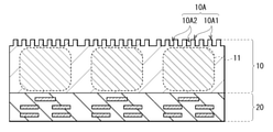
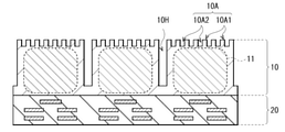
- FIG. 1 It is sectional drawing which shows an example of the structure of the image pickup device which concerns on one Embodiment of this disclosure. It is a block diagram which shows the whole structure of the image pickup element shown in FIG. It is an equivalent circuit diagram of the image pickup device shown in FIG. It is a schematic diagram explaining an example of the concavo-convex structure of the light receiving surface of the image pickup element shown in FIG. 1 and the cross-sectional structure in the vicinity thereof. It is a characteristic diagram which simulated the diffraction amount of visible light by the pitch size of the concavo-convex structure. It is a figure which simulated the relationship between the width and depth of the concave part which constitutes the concave-convex structure, and the reflection characteristic of a light receiving surface.
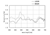
- FIG. 11A It is sectional drawing which shows the process following FIG. 11B. It is sectional drawing which shows the process following FIG. 11C. It is sectional drawing which shows the process following FIG. 11D. It is sectional drawing which shows the process following FIG. 11E. It is sectional drawing which shows the process following FIG. 11F. It is sectional drawing which shows the process following FIG. 11G. It is a figure which shows the reflection characteristic of visible light on the light receiving surface by the presence or absence of an uneven structure.
- Embodiment an example of an image pickup device having a reflectance adjusting layer composed of a plurality of convex portions of a concave-convex structure provided on a light-receiving surface and a passivation film embedded in a plurality of concave portions of the concave-convex structure on the light-receiving surface.
- Embodiment an example of an image pickup device having a reflectance adjusting layer composed of a plurality of convex portions of a concave-convex structure provided on a light-receiving surface and a passivation film embedded in a plurality of concave portions of the concave-convex structure on the light-receiving surface.
- FIG. 1 schematically shows a cross-sectional configuration example of an image pickup device 1 as an example of a photodetector according to an embodiment of the present disclosure.
- FIG. 2 shows an example of the overall configuration of the image pickup device 1 shown in FIG.
- the image pickup element 1 is, for example, a CMOS (Complementary Metal Oxide Semiconductor) image sensor used in electronic devices such as digital still cameras and video cameras, and is a pixel in which a plurality of pixels are two-dimensionally arranged in a matrix as an image pickup area. It has a unit (pixel unit 100A).
- the image pickup element 1 is a so-called back-illuminated image pickup element that constitutes, for example, one pixel (unit pixel P) in this CMOS image sensor or the like.
- the image pickup device 1 of the present embodiment has the reflectance adjusting layer 10X on the light receiving surface (first surface) 10S1 of the semiconductor substrate 10 in which the photoelectric conversion unit 11 is embedded and formed.
- the reflectance adjusting layer 10X includes a plurality of convex portions 10A1 constituting the concave-convex structure 10A provided on the first surface 10S1 of the semiconductor substrate 10 and a passivation film 12 embedded in a plurality of concave portions 10A2 constituting the concave-convex structure 10A. It is a pseudo high reflectance layer composed of, and has a refractive index between the semiconductor substrate 10 and the passivation film 12.
- the image sensor 1 captures incident light (image light) from a subject via an optical lens system (not shown), and converts the amount of incident light imaged on the image pickup surface into an electric signal on a pixel-by-pixel basis. It is output as a pixel signal.
- the image pickup element 1 has a pixel portion 100A as an imaging area on the semiconductor substrate 10, and in a peripheral region of the pixel portion 100A, for example, a vertical drive circuit 111, a column signal processing circuit 112, a horizontal drive circuit 113, and an output. It has a circuit 114, a control circuit 115, and an input / output terminal 116.
- a pixel drive line Lread (specifically, a row selection line and a reset control line) is wired for each pixel row, and a vertical signal line Lsig is wired for each pixel column.
- the pixel drive line Lead transmits a drive signal for reading a signal from the pixel.
- One end of the pixel drive line Lead is connected to the output end corresponding to each line of the vertical drive circuit 111.
- the vertical drive circuit 111 is configured by a shift register, an address decoder, or the like, and is a pixel drive unit that drives each unit pixel P of the pixel unit 100A, for example, in row units.
- the signal output from each unit pixel P of the pixel row selectively scanned by the vertical drive circuit 111 is supplied to the column signal processing circuit 112 through each of the vertical signal lines Lsig.
- the column signal processing circuit 112 is composed of an amplifier, a horizontal selection switch, and the like provided for each vertical signal line Lsig.
- the horizontal drive circuit 113 is composed of a shift register, an address decoder, etc., and drives each horizontal selection switch of the column signal processing circuit 112 in order while scanning. By the selective scanning by the horizontal drive circuit 113, the signals of each pixel transmitted through each of the vertical signal lines Lsig are sequentially output to the horizontal signal line 121 and transmitted to the outside of the semiconductor substrate 10 through the horizontal signal line 121. ..
- the output circuit 114 processes signals and outputs the signals sequentially supplied from each of the column signal processing circuits 112 via the horizontal signal line 121.
- the output circuit 114 may, for example, perform only buffering, or may perform black level adjustment, column variation correction, various digital signal processing, and the like.
- the circuit portion including the vertical drive circuit 111, the column signal processing circuit 112, the horizontal drive circuit 113, the horizontal signal line 121, and the output circuit 114 may be formed directly on the semiconductor substrate 10, or may be used as an external control IC. It may be arranged. Further, those circuit portions may be formed on another substrate connected by a cable or the like.
- the control circuit 115 receives a clock given from the outside of the semiconductor substrate 10, data instructing an operation mode, and the like, and outputs data such as internal information of the image pickup device 1.
- the control circuit 115 further has a timing generator that generates various timing signals, and the vertical drive circuit 111, the column signal processing circuit 112, the horizontal drive circuit 113, and the like based on the various timing signals generated by the timing generator. It controls the drive of peripheral circuits.
- the input / output terminal 116 exchanges signals with the outside.
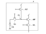
- FIG. 3 shows an example of a readout circuit of the unit pixel P of the image pickup device 1 shown in FIG.
- the unit pixel P has, for example, a photoelectric conversion unit 11, a transfer transistor TR, a floating diffusion FD, a reset transistor RST, an amplification transistor AMP, and a selection transistor SEL. ..
- the photoelectric conversion unit 11 is, for example, a photodiode (PD).
- the anode is connected to the ground voltage line and the cathode is connected to the source of the transfer transistor TR.
- the transfer transistor TR is connected between the photoelectric conversion unit 11 and the floating diffusion FD.
- a drive signal TRsig is applied to the gate electrode of the transfer transistor TR.
- this drive signal TRsig becomes active, the transfer gate of the transfer transistor TR becomes conductive, and the signal charge stored in the photoelectric conversion unit 11 is transferred to the floating diffusion FD via the transfer transistor TR.
- the floating diffusion FD is connected between the transfer transistor TR and the amplification transistor AMP.
- the floating diffusion FD converts the signal charge transferred by the transfer transistor TR into a voltage signal and outputs it to the amplification transistor AMP.
- the reset transistor RST is connected between the floating diffusion FD and the power supply unit.
- a drive signal RSTsig is applied to the gate electrode of the reset transistor RST.
- this drive signal RSTsig becomes active, the reset gate of the reset transistor RST becomes conductive, and the potential of the floating diffusion FD is reset to the level of the power supply unit.
- the gate electrode of the amplification transistor AMP is connected to the floating diffusion FD, and the drain electrode is connected to the power supply unit, which serves as an input unit for a voltage signal reading circuit held by the floating diffusion FD, a so-called source follower circuit. That is, the amplification transistor AMP constitutes a constant current source and a source follower circuit connected to one end of the vertical signal line Lsig by connecting its source electrode to the vertical signal line Lsig via the selection transistor SEL.
- the selection transistor SEL is connected between the source electrode of the amplification transistor AMP and the vertical signal line Lsig.
- a drive signal SELsig is applied to the gate electrode of the selection transistor SEL.
- the selection transistor SEL becomes a conduction state, and the unit pixel P becomes a selection state.
- the read signal (pixel signal) output from the amplification transistor AMP is output to the vertical signal line Lsig via the selection transistor SEL.
- the image pickup device 1 has a configuration in which a semiconductor substrate 10 in which a photoelectric conversion unit 11 is embedded and a multilayer wiring layer 20 having a plurality of wiring layers (for example, wiring layers 21, 22, 23) are laminated. There is.
- the semiconductor substrate 10 has a first surface 10S1 (back surface) and a second surface 10S2 (front surface) facing each other, and the multilayer wiring layer 20 is provided on the second surface 10S2 of the semiconductor substrate 10.
- a passivation film 12 On the first surface 10S1 of the semiconductor substrate 10, a passivation film 12, a first antireflection layer 13, a second antireflection layer 14, for example, a color filter 15 and a light shielding film 16 provided in the same surface, and a lens.
- the layers 17 are laminated in this order.
- the semiconductor substrate 10 is composed of, for example, a silicon (Si) substrate or an indium gallium arsenic (InGaAs) substrate.
- the photoelectric conversion unit 11 is, for example, a PIN (Positive Intrinsic Negative) type photodiode (PD), and has a pn junction in a predetermined region of the semiconductor substrate 10. As described above, the photoelectric conversion unit 11 is embedded and formed one by one for each unit pixel P.
- a fine uneven structure 10A is formed on the first surface 10S1 of the semiconductor substrate 10.
- the first surface 10S1 of the semiconductor substrate 10 is further provided with a separation portion 10B extending from the first surface 10S1 toward the second surface 10S2.
- the uneven structure 10A constitutes the reflectance adjusting layer 10X, and although details will be described later, it is composed of a plurality of convex portions 10A1 and a plurality of concave portions 10A2 provided on the first surface 10S1 of the semiconductor substrate 10. There is.
- the separation unit 10B is provided between adjacent unit pixels P.
- the separation unit 10B is provided so as to surround the unit pixel P, and is provided on the entire pixel unit 100A in a plan view, for example, in a grid pattern.
- the separation unit 10B is for electrically separating adjacent unit pixels P.
- the separation unit 10B extends from the first surface 10S1 side of the semiconductor substrate 10 toward the second surface 10S2, and is, for example, in the semiconductor substrate 10. Has a bottom. Further, the separation portion 10B may penetrate between the first surface 10S1 side and the second surface 10S2 of the semiconductor substrate 10.
- the passivation film 12 protects the light receiving surface (first surface 10S1) of the semiconductor substrate 10 and constitutes the reflectance adjusting layer 10X.
- the passivation film 12 is laminated on the first surface 10S1 of the semiconductor substrate 10 and also has a plurality of recesses 10A2 constituting the concave-convex structure 10A and a groove 10H constituting the separation portion 10B embedded therein. As shown in FIG. 4, for example, a wavy structure corresponding to the uneven structure 10A is formed on the surface of the passivation film 12.
- Examples of the material constituting the passivation film 12 include a material having a refractive index smaller than that of the semiconductor substrate 10.
- Specific materials of the passivation film 12 include, for example, hafnium (Hf), aluminum (Al), titanium (Ti), zirconium (Zr), tantalum (Ta), yttrium (Y) and strontium (Sr). Examples thereof include an oxide film or a nitride film containing at least one species.
- the first antireflection layer 13 is for reducing the reflection of light incident from the light incident side S1 on the light receiving surface (first surface 10S1) of the semiconductor substrate 10. Similar to the passivation film 12, a wavy structure corresponding to the uneven structure 10A is formed on the surface of the first antireflection layer 13, for example, as shown in FIG.
- the material constituting the first antireflection layer 13 examples include a material having a refractive index smaller than that of the semiconductor substrate 10, similar to the passivation film 12.
- Specific materials of the first antireflection layer 13 include, for example, hafnium (Hf), aluminum (Al), titanium (Ti), zirconium (Zr), tantalum (Ta), yttrium (Y) and strontium (Sr). An oxide film or a nitride film containing at least one of these can be mentioned.
- the second antireflection layer 14 is for reducing the reflection of light incident from the light incident side S1 on the light receiving surface (first surface 10S1) of the semiconductor substrate 10 and flattening the surface of the light incident side S1. It is a thing.
- the material constituting the second antireflection layer 14 include a material having a refractive index smaller than that of the material constituting the first antireflection layer 13.
- Specific examples of the material of the second antireflection layer 14 include silicon oxide (SiO x ), silicon nitride (SiN x ), silicon oxynitride (SiO x N y ), and the like.
- the color filter 15 is provided on the light incident side S1 of the semiconductor substrate 10, and for example, a color that selectively transmits, for example, red light (R), green light (G), or blue light (B) for each unit pixel P. It has filters 15R, 15G and 15B.
- a color that selectively transmits for example, red light (R), green light (G), or blue light (B) for each unit pixel P.
- It has filters 15R, 15G and 15B.
- two color filters 15G that selectively transmit green light (G) are arranged diagonally with respect to four unit pixels P arranged in 2 rows ⁇ 2 columns.
- the color filters 15R and 15B that selectively transmit the red light (R) and the blue light (B) are arranged one by one on orthogonal diagonal lines.
- the unit pixel P provided with the color filters 15R, 15G, and 15B for example, the corresponding color light is detected by each photoelectric conversion unit 11. That is, in the pixel unit 100A, the unit pixels P for detecting the red light (R), the green light (G), and the blue light (B) are arranged in a Bayer shape, respectively.
- the light-shielding film 16 is for preventing light obliquely incident on the color filter 15 from leaking to an adjacent unit pixel P.
- the light-shielding film 16 is provided between the adjacent color filters 15R, 15G, and 15B, for example, in the same plane as the color filter 15. That is, the light-shielding film 16 is provided on the entire pixel portion 100A in a planar view, for example, in the same manner as the separation portion 19B.
- the material constituting the light-shielding film 16 include a conductive material having a light-shielding property. Specific examples thereof include tungsten (W), silver (Ag), copper (Cu), aluminum (Al), and alloys of Al and copper (Cu).
- the lens layer 27 is provided so as to cover the entire surface of the pixel portion 100A, and has, for example, a plurality of on-chip lenses 17L provided for each unit pixel P on the surface thereof.
- the on-chip lens 17L is for condensing the light incident from above on the photoelectric conversion unit 11.
- the lens layer 27 is formed of, for example, an inorganic material such as silicon oxide (SiO x ) or silicon nitride (SiN x).
- the lens layer 27 may be formed by using an organic material having a high refractive index such as an episulfide resin, a thietan compound or the resin thereof.
- the shape of the on-chip lens 17L is not particularly limited, and various lens shapes such as a hemispherical shape and a semi-cylindrical shape can be adopted.
- the multilayer wiring layer 20 is provided on the side opposite to the light incident side S1, specifically, on the second surface 10S2 side of the semiconductor substrate 10.
- the multilayer wiring layer 20 has, for example, a configuration in which a plurality of wiring layers 21, 22, and 23 are laminated with an interlayer insulating layer 24 in between.
- the multilayer wiring layer 20 is formed with, for example, a vertical drive circuit 111, a column signal processing circuit 112, a horizontal drive circuit 113, an output circuit 114, a control circuit 115, an input / output terminal 116, and the like. There is.
- the wiring layers 21, 22, and 23 are formed of, for example, aluminum (Al), copper (Cu), tungsten (W), or the like.
- the wiring layers 21, 22, and 23 may be formed by using polysilicon (Poly—Si).
- the interlayer insulating layer 34 is, for example, a single-layer film made of one of silicon oxide (SiO x ), TEOS, silicon nitride (SiN x ), silicon oxynitride (SiO x N y ), and the like, or among these. It is formed of a laminated film composed of two or more types.
- the image pickup device 1 of the present embodiment has a reflectance adjusting layer 10X having a refractive index of, for example, about 3 on the light receiving surface (first surface 10S1).
- the reflectance adjusting layer 10X is for suppressing reflection and diffraction of incident light on the first surface 10S1.
- the reflectance adjusting layer 10X is embedded in the plurality of convex portions 10A1 constituting the concave-convex structure 10A provided on the first surface 10S1 of the semiconductor substrate 10 and the plurality of concave portions 10A2 constituting the concave-convex structure 10A. It is composed of a passivation film 12.
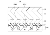
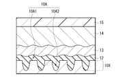
- FIG. 4 is an enlarged representation of the cross-sectional configuration of the light receiving surface (first surface 10S1) of the semiconductor substrate 10 shown in FIG. 1 and its vicinity (X in the figure).
- a concave-convex structure 10A composed of a plurality of convex portions 10A1 and a plurality of concave portions 10A2 having a predetermined hole diameter (width: w), depth (h), and pitch size (l) is formed on the first surface 10S1 of the semiconductor substrate 10.
- the passivation film 12 is laminated on the first surface 10S1 of the semiconductor substrate 10, and the plurality of recesses 10A2 are embedded by the passivation film 12.
- the reflectance adjusting layer 10X simulates the surface structure of the semiconductor substrate 10 including the plurality of convex portions 10A1 constituting the concave-convex structure 10A and the passivation film 12 embedded in the plurality of concave portions 10A2 constituting the concave-convex structure 10A. It is regarded as a layer. Therefore, the reflectance adjusting layer 10X has a refractive index averaged by the volume ratio of the semiconductor substrate 10 which is a component and the passivation film 12.
- the refractive indexes n 10 , n 13 , and n 14 of the first antireflection layer 13 and the second antireflection layer 14 laminated on the semiconductor substrate 10 and the light receiving surface (first surface 10S1) thereof are different. It has a relationship of n 10 > n 13 > n 14. The number at the end corresponds to the code of each component.
- the reflectance adjusting layer 10X has a refractive index n 10X averaged by the volume ratio of the semiconductor substrate 10 and the passivation film 12.
- the reflectivity adjustment layer 10X the semiconductor substrate 10 and the light receiving surface thereof plus (first surface 10S1) to stacked layers of refractive index n 10, n 10X, n 13 , n 14 , the semiconductor from the light incident side S1 It is configured to gradually increase toward the substrate 10 (n 10 > n 10X > n 13 > n 14 ).
- the oxide films mentioned as the materials of the first antireflection layer 13 and the second antireflection layer 14 have the following refractive indexes, respectively.
- the numerical value in () is the refractive index for a wavelength near 550 nm.
- the material constituting the second antireflection layer 14 As an example, when a silicon substrate (Si; 4.1) is used as the semiconductor substrate 10 and silicon oxide (SiO x ; 1.3 to 1.5) is used as the material constituting the second antireflection layer 14, As the material constituting the first antireflection layer 13, for example, tantalum oxide (TaO x ; 2.2) can be selected. Further, for the passivation film 12 constituting the reflectance adjusting layer 10X, for example, aluminum oxide (AlO x ; 1.63) is selected. In that case, the refractive index n 10X of the reflectance adjusting layer 10X is a value averaged by the volume ratio of the constituent semiconductor substrate 10 and the passivation film 12, and is, for example, 2.6 to 3.7. As a result, the reflection of the incident light on the light receiving surface 10S1 is suppressed.
- the concave-convex structure 10A of the light receiving surface (first surface 10S1) of the semiconductor substrate 10 has a predetermined shape.
- FIG. 5 is a simulation result of the diffraction amount of visible light (for example, wavelength 400 nm to 750 nm) due to the distance (pitch size l) between a plurality of adjacent recesses 10A2 constituting the concave-convex structure 10A.
- the pitch size l of the uneven structure 10A By setting the pitch size l of the uneven structure 10A to 200 nm or less, the diffraction amount of visible light is reduced to about 70%, and by setting the pitch size l of the uneven structure 10A to 150 nm or less, the diffraction amount of visible light is 50. It is reduced to about%.
- the pitch size l of the uneven structure 10A is 100 nm or less, the diffraction amount of visible light is reduced to 20% or less, and by setting the pitch size l of the uneven structure 10A to 50 nm or less, the visible light is almost diffracted. It disappears.
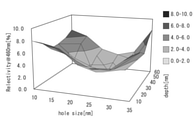
- FIG. 6 is a result of simulating the relationship between the width w and the depth h of the plurality of recesses 10A2 constituting the concave-convex structure 10A and the reflection characteristics of the light receiving surface (first surface 10S1). For example, by setting the width w of the recess 10A2 to 15 nm or more and 30 nm or less and the depth h of the recess 10A2 to 10 nm or more and 60 nm or less, the reflectance of light having a wavelength of 460 nm is 8% or less.
- the reflectance of light having a wavelength of 460 nm is 2% or less.
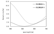
- FIG. 7 is a simulation result of the reflection characteristics of the light receiving surface (first surface 10S1) depending on the presence or absence of the concave-convex structure 10A.
- the pitch size l of the concave-convex structure 10A and the width w and the depth h of the plurality of concave portions 10A2 constituting the concave-convex structure 10A are in the following ranges. That is, the pitch size l of the uneven structure 10A is preferably, for example, 200 nm or less, and more preferably 100 nm or less.
- the width w of the plurality of recesses 10A2 constituting the concave-convex structure 10A is preferably, for example, 15 nm or more and 30 nm or less, and more preferably 20 nm or more and 25 nm or less.
- the depth h of the plurality of recesses 10A2 constituting the concave-convex structure 10A is preferably, for example, 10 nm or more and 60 nm or less, and more preferably 40 nm or more and 50 nm or less.
- FIG. 8 shows the change in quantum efficiency depending on the thickness of the first antireflection layer 13 (for example, TaO x film).
- the thickness of the first antireflection layer 13 made of the TaO x film is 75 nm, the quantum efficiency is about 63%.
- the quantum efficiency is improved to 65% or more.
- the thickness of the first antireflection layer 13 is preferably, for example, 75 nm or less, and more preferably 55 nm or less.
- the cross-sectional shape of the plurality of recesses 10A2 constituting the concave-convex structure 10A has, for example, a side surface substantially perpendicular to the first surface 10S1 and a bottom surface parallel to the first surface 10S1 as shown in FIG. Not limited.
- the cross-sectional shape of the recess 10A2 may be a tapered shape that gradually narrows from the first surface 10S1 to the second surface 10S2.
- the cross-sectional shape of the recess 10A2 may be a curved surface shape in which the side surface and the bottom surface of the recess 10A2 are continuous, for example, as shown in FIG. 9B.
- the surfaces of the passivation film 12 and the first antireflection layer 13 have a wavy shape according to the uneven structure 10A, and the surface areas of the passivation film 12 and the first antireflection layer 13 increase.
- the first antireflection layer 13 is formed by, for example, plasma oxidation, the area of the first antireflection layer 13 exposed to plasma is expanded, and the pinning effect is added to the first antireflection layer 13. Therefore, it is possible to reduce the generation of dark current on the light receiving surface (first surface 10S1) side.
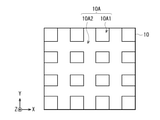
- planar patterns of the plurality of recesses 10A2 constituting the concave-convex structure 10A may be regularly formed in the X direction and the Y direction, for example, as shown in FIG. 10A.
- the planar pattern of the plurality of recesses 10A2 constituting the concave-convex structure 10A has a lattice shape in which the recesses 10A2 regularly formed in the X direction and the Y direction are continuous with each other, as shown in FIG. 10B, for example. You may be doing it.
- FIGS. 10A and 10B show an example in which a plurality of recesses 10A2 are regularly formed, they may be randomly formed.
- the average value of the plurality of recesses 10A2 within a predetermined range such as the unit pixel P is the pitch size l of the concave-convex structure 10A described above, the width w and the depth of the plurality of recesses 10A2 constituting the concave-convex structure 10A. It suffices if the h is satisfied.
- the image pickup device 1 of the present embodiment can be formed, for example, as follows.
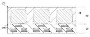
- the photoelectric conversion unit 11 is formed in the semiconductor substrate 10. Subsequently, although not shown, after forming various transistors constituting the floating diffusion FD and the readout circuit on the second surface 10S2 side of the semiconductor substrate 10, wiring layers 21, 22, 23 as shown in FIG. 11A. And the multilayer wiring layer 20 including the interlayer insulating layer 24 is formed.
- the concave-convex structure 10A and the separation portion 10B are formed on the first surface 10S1 of the semiconductor substrate 10.
- the concave-convex structure 10A of the first surface 10S1 can be formed by using, for example, a self-organizing technique (DSA).
- DSA self-organizing technique
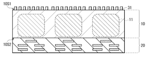
- the hard mask 31 and the intermediate layer 32 are formed on the first surface 10S1 of the semiconductor substrate 10.
- the intermediate layer 32 is coated with the diblock copolymer, annealed, and etched.
- a mask 33 having a predetermined pattern is formed on the intermediate layer 32.
- the pattern thus formed has, for example, a hexagonal fine structure in a plan view.
- the hard mask 31 is etched.
- the pattern of the mask 33 is transferred to the hard mask 31.
- FIG. 11D by etching the semiconductor substrate 10, a plurality of fine recesses 10A2 are formed on the first surface 10S1 of the semiconductor substrate 10.
- a groove 10H is formed between adjacent photoelectric conversion units 11 by etching.
- an AlO x film is formed to embed the recess 10A2 and the groove 10H.
- a TaO x film as the first antireflection layer 13 and a SiO x film as the second antireflection layer 14 are formed in order.
- the surface of the second antireflection layer 14 is flattened by CMP (Chemical Mechanical Polishing).
- CMP Chemical Mechanical Polishing
- a light-shielding film 16 is formed on the second antireflection layer 14.
- the color filter 15 (15R, 15G, 15B) and the lens layer 17 are formed in order.
- the image pickup device 1 shown in FIG. 1 is completed.
- the concave-convex structure 10A is provided on the light receiving surface (first surface 10S1) of the semiconductor substrate 10 having the photoelectric conversion unit 11, and the passivation film 12 is provided with a plurality of concave portions 10A2 constituting the concave-convex structure 10A.
- the first surface 10S1 is provided with a reflectance adjusting layer 10X composed of a plurality of convex portions 10A1 constituting the concave-convex structure 10A and a passivation film 12 in which a plurality of concave portions 10A2 are embedded. This suppresses reflection and diffraction in a wide wavelength band on the light receiving surface (first surface 10S1). This will be described below.
- image sensors have been required to be smaller and have higher definition.
- the sensitivity decreases when the pixels are reduced, improvement in the sensitivity is required for a high-definition image sensor.
- incident light is reflected, for example, on the surface of a Si substrate.
- the intensity of the light reaching the light receiving portion is lost, the sensitivity is lowered, and flare and ghost are generated by the incident light from the unintended optical path.
- the light receiving surface (first surface 10S1) of the semiconductor substrate 10 is provided with a concavo-convex structure 10A composed of a plurality of convex portions 10A1 and a plurality of concave portions 10A2. Further, the passivation film 12 is laminated on the first surface 10S1 of the semiconductor substrate 10 to embed a plurality of recesses 10A2.
- the first surface 10S1 of the semiconductor substrate 10 the refractive index n 10 of the semiconductor substrate 10
- the refractive index n 10x between the refractive index n 13 of the first anti-reflection layer 13 laminated on the passivation film 12
- the refractive index adjusting layer 10X having the above is formed.
- FIG. 12 shows the reflection characteristics of visible light on the light receiving surface (first surface 10S1) depending on whether the concave-convex structure 10A is present (Example) or not (comparative example).
- FIG. 13 shows the relative quantum efficiencies of red light (R), green light (G), and blue light (B) depending on whether the concave-convex structure 10A is present (Example) or not (comparative example).
- the reflectance of the blue light (B) on the short wavelength side of the visible light is significantly reduced, and the quantum efficiency of the blue light (B) is improved accordingly.
- the image pickup device 1 of the present embodiment it is possible to suppress the reflection of incident light in a wide wavelength band on the first surface 10S1 while reducing the generation of diffracted light on the first surface 10S1. .. Therefore, it is possible to improve the sensitivity while suppressing the occurrence of color mixing due to crosstalk. That is, it becomes possible to provide a highly sensitive photodetector.
- the pitch size l of the concave-convex structure 10A is set to, for example, 200 nm or less, more preferably 100 nm or less.
- the width w of the plurality of recesses 10A2 constituting the uneven structure 10A is, for example, 15 nm or more and 30 nm or less, more preferably 20 nm or more and 25 nm or less.
- the depth h of the plurality of recesses 10A2 constituting the concave-convex structure 10A was, for example, 10 nm or more and 60 nm or less, more preferably 40 nm or more and 50 nm or less.
- the surfaces of the passivation film 12 and the first antireflection layer 13 have a wavy structure corresponding to the uneven structure 10A.
- the surface area of the first antireflection layer 13 is expanded, and the first antireflection layer 13 has a function as a fixed charge layer. Therefore, it is possible to reduce the generation of dark current on the light receiving surface (first surface 10S1) side.
- the thickness of the image pickup device 1 can be reduced as compared with the case where the above-mentioned moth-eye structure is provided. Therefore, it is possible to realize a compact and highly sensitive image sensor.
- the image sensor 1 can be applied to all types of electronic devices having an image pickup function, such as a camera system such as a digital still camera or a video camera, and a mobile phone having an image pickup function.
- FIG. 14 shows a schematic configuration of the electronic device 1000.
- the electronic device 1000 includes, for example, a lens group 1001, an image pickup element 1, a DSP (Digital Signal Processor) circuit 1002, a frame memory 1003, a display unit 1004, a recording unit 1005, an operation unit 1006, and a power supply unit 1007. And are connected to each other via the bus line 1008.
- a lens group 1001 an image pickup element 1
- a DSP (Digital Signal Processor) circuit 1002 a frame memory 1003, a display unit 1004, a recording unit 1005, an operation unit 1006, and a power supply unit 1007. And are connected to each other via the bus line 1008.
- DSP Digital Signal Processor
- the lens group 1001 captures incident light (image light) from the subject and forms an image on the image pickup surface of the image pickup device 1.
- the image pickup element 1 converts the amount of incident light imaged on the image pickup surface by the lens group 1001 into an electric signal in pixel units and supplies it to the DSP circuit 1002 as a pixel signal.
- the DSP circuit 1002 is a signal processing circuit that processes a signal supplied from the image pickup device 1.
- the DSP circuit 1002 outputs image data obtained by processing a signal from the image sensor 1.
- the frame memory 1003 temporarily holds the image data processed by the DSP circuit 1002 in many frames.
- the display unit 1004 is composed of a panel-type display device such as a liquid crystal panel or an organic EL (Electro Luminescence) panel, and records image data of a moving image or a still image captured by the image pickup element 1 as a recording medium such as a semiconductor memory or a hard disk. Record in.
- a panel-type display device such as a liquid crystal panel or an organic EL (Electro Luminescence) panel
- image data of a moving image or a still image captured by the image pickup element 1 as a recording medium such as a semiconductor memory or a hard disk. Record in.
- the operation unit 1006 outputs operation signals for various functions owned by the electronic device 1000 according to the operation by the user.
- the power supply unit 1007 appropriately supplies various power sources that serve as operating power sources for the DSP circuit 1002, the frame memory 1003, the display unit 1004, the recording unit 1005, and the operation unit 1006.
- the image pickup device 1 can be applied to the following electronic devices.
- FIG. 15 shows an example of using the image pickup device 1 according to the above embodiment.
- the image pickup device 1 is used in various cases for sensing light such as visible light, infrared light, ultraviolet light, and X-ray, as described below, in addition to the electronic device having the above-mentioned image pickup function. be able to.
- Devices that take images for viewing such as digital cameras and portable devices with camera functions.
- Devices and user gestures used for traffic such as in-vehicle sensors that capture images of the rear, surroundings, and interior of vehicles, surveillance cameras that monitor traveling vehicles and roads, and distance measuring sensors that measure distance between vehicles.
- devices and endoscopes used in home appliances such as televisions, refrigerators, and air conditioners, and devices that perform angiography by receiving infrared light.
- Equipment used for medical and healthcare surveillance cameras for crime prevention, cameras for person authentication, etc., equipment used for security, skin measuring instruments for taking pictures of the skin, and scalp Devices used for beauty such as microscopes for taking pictures, action cameras and wearable cameras for sports applications, devices used for sports, cameras for monitoring the condition of fields and crops, etc.
- the technology according to the present disclosure can be applied to various products.
- the technology according to the present disclosure is realized as a device mounted on a moving body of any kind such as an automobile, an electric vehicle, a hybrid electric vehicle, a motorcycle, a bicycle, a personal mobility, an airplane, a drone, a ship, and a robot. You may.
- FIG. 16 is a block diagram showing a schematic configuration example of a vehicle control system, which is an example of a mobile control system to which the technique according to the present disclosure can be applied.
- the vehicle control system 12000 includes a plurality of electronic control units connected via the communication network 12001.
- the vehicle control system 12000 includes a drive system control unit 12010, a body system control unit 12020, an outside information detection unit 12030, an in-vehicle information detection unit 12040, and an integrated control unit 12050.
- a microcomputer 12051, an audio image output unit 12052, and an in-vehicle network I / F (interface) 12053 are shown as a functional configuration of the integrated control unit 12050.
- the drive system control unit 12010 controls the operation of the device related to the drive system of the vehicle according to various programs.
- the drive system control unit 12010 has a driving force generator for generating a driving force of a vehicle such as an internal combustion engine or a driving motor, a driving force transmission mechanism for transmitting the driving force to the wheels, and a steering angle of the vehicle. It functions as a control device such as a steering mechanism for adjusting and a braking device for generating braking force of the vehicle.
- the body system control unit 12020 controls the operation of various devices mounted on the vehicle body according to various programs.
- the body system control unit 12020 functions as a keyless entry system, a smart key system, a power window device, or a control device for various lamps such as headlamps, back lamps, brake lamps, turn signals or fog lamps.
- the body system control unit 12020 may be input with radio waves transmitted from a portable device that substitutes for the key or signals of various switches.
- the body system control unit 12020 receives inputs of these radio waves or signals and controls a vehicle door lock device, a power window device, a lamp, and the like.
- the vehicle outside information detection unit 12030 detects information outside the vehicle equipped with the vehicle control system 12000.
- the image pickup unit 12031 is connected to the vehicle outside information detection unit 12030.
- the vehicle outside information detection unit 12030 causes the image pickup unit 12031 to capture an image of the outside of the vehicle and receives the captured image.
- the out-of-vehicle information detection unit 12030 may perform object detection processing or distance detection processing such as a person, a vehicle, an obstacle, a sign, or a character on the road surface based on the received image.
- the image pickup unit 12031 is an optical sensor that receives light and outputs an electric signal according to the amount of the light received.
- the image pickup unit 12031 can output an electric signal as an image or can output it as distance measurement information. Further, the light received by the image pickup unit 12031 may be visible light or invisible light such as infrared light.
- the in-vehicle information detection unit 12040 detects the in-vehicle information.
- a driver state detection unit 12041 that detects the driver's state is connected to the in-vehicle information detection unit 12040.
- the driver state detection unit 12041 includes, for example, a camera that images the driver, and the in-vehicle information detection unit 12040 determines the degree of fatigue or concentration of the driver based on the detection information input from the driver state detection unit 12041. It may be calculated, or it may be determined whether or not the driver has fallen asleep.
- the microcomputer 12051 calculates the control target value of the driving force generator, the steering mechanism, or the braking device based on the information inside and outside the vehicle acquired by the vehicle exterior information detection unit 12030 or the vehicle interior information detection unit 12040, and the drive system control unit.
- a control command can be output to 12010.
- the microcomputer 12051 realizes ADAS (Advanced Driver Assistance System) functions including vehicle collision avoidance or impact mitigation, follow-up driving based on inter-vehicle distance, vehicle speed maintenance driving, vehicle collision warning, vehicle lane deviation warning, and the like. It is possible to perform cooperative control for the purpose of.
- ADAS Advanced Driver Assistance System
- the microcomputer 12051 controls the driving force generating device, the steering mechanism, the braking device, and the like based on the information around the vehicle acquired by the vehicle exterior information detection unit 12030 or the vehicle interior information detection unit 12040. It is possible to perform coordinated control for the purpose of automatic driving that runs autonomously without depending on the operation.
- the microcomputer 12051 can output a control command to the body system control unit 12020 based on the information outside the vehicle acquired by the vehicle outside information detection unit 12030.
- the microcomputer 12051 controls the headlamps according to the position of the preceding vehicle or the oncoming vehicle detected by the outside information detection unit 12030, and performs cooperative control for the purpose of anti-glare such as switching the high beam to the low beam. It can be carried out.
- the audio image output unit 12052 transmits an output signal of at least one of audio and image to an output device capable of visually or audibly notifying information to the passenger or the outside of the vehicle.
- an audio speaker 12061, a display unit 12062, and an instrument panel 12063 are exemplified as output devices.
- the display unit 12062 may include, for example, at least one of an onboard display and a head-up display.
- FIG. 17 is a diagram showing an example of the installation position of the image pickup unit 12031.
- the vehicle 12100 has an imaging unit 12101, 12102, 12103, 12104, 12105 as an imaging unit 12031.
- the image pickup units 12101, 12102, 12103, 12104, 12105 are provided, for example, at positions such as the front nose, side mirrors, rear bumpers, back doors, and the upper part of the windshield in the vehicle interior of the vehicle 12100.
- the image pickup unit 12101 provided in the front nose and the image pickup section 12105 provided in the upper part of the windshield in the vehicle interior mainly acquire an image in front of the vehicle 12100.
- the image pickup units 12102 and 12103 provided in the side mirror mainly acquire images of the side of the vehicle 12100.
- the image pickup unit 12104 provided in the rear bumper or the back door mainly acquires an image of the rear of the vehicle 12100.
- the images in front acquired by the image pickup units 12101 and 12105 are mainly used for detecting a preceding vehicle, a pedestrian, an obstacle, a traffic light, a traffic sign, a lane, or the like.
- FIG. 17 shows an example of the shooting range of the imaging units 12101 to 12104.
- the imaging range 12111 indicates the imaging range of the imaging unit 12101 provided on the front nose
- the imaging ranges 12112 and 12113 indicate the imaging range of the imaging units 12102 and 12103 provided on the side mirrors, respectively
- the imaging range 12114 indicates the imaging range.
- the imaging range of the imaging unit 12104 provided on the rear bumper or the back door is shown. For example, by superimposing the image data captured by the image pickup units 12101 to 12104, a bird's-eye view image of the vehicle 12100 can be obtained.
- At least one of the image pickup units 12101 to 12104 may have a function of acquiring distance information.
- at least one of the image pickup units 12101 to 12104 may be a stereo camera including a plurality of image pickup elements, or may be an image pickup element having pixels for phase difference detection.
- the microcomputer 12051 has a distance to each three-dimensional object within the image pickup range 12111 to 12114 based on the distance information obtained from the image pickup unit 12101 to 12104, and a temporal change of this distance (relative speed with respect to the vehicle 12100). By obtaining can. Further, the microcomputer 12051 can set an inter-vehicle distance to be secured in advance in front of the preceding vehicle, and can perform automatic brake control (including follow-up stop control), automatic acceleration control (including follow-up start control), and the like. In this way, it is possible to perform coordinated control for the purpose of automatic driving or the like in which the vehicle travels autonomously without depending on the operation of the driver.
- automatic brake control including follow-up stop control
- automatic acceleration control including follow-up start control
- the microcomputer 12051 converts three-dimensional object data related to a three-dimensional object into two-wheeled vehicles, ordinary vehicles, large vehicles, pedestrians, electric poles, and other three-dimensional objects based on the distance information obtained from the image pickup units 12101 to 12104. It can be classified and extracted and used for automatic avoidance of obstacles. For example, the microcomputer 12051 distinguishes obstacles around the vehicle 12100 into obstacles that are visible to the driver of the vehicle 12100 and obstacles that are difficult to see. Then, the microcomputer 12051 determines the collision risk indicating the risk of collision with each obstacle, and when the collision risk is equal to or higher than the set value and there is a possibility of collision, the microcomputer 12051 via the audio speaker 12061 or the display unit 12062. By outputting an alarm to the driver and performing forced deceleration and avoidance steering via the drive system control unit 12010, driving support for collision avoidance can be provided.
- At least one of the image pickup units 12101 to 12104 may be an infrared camera that detects infrared rays.
- the microcomputer 12051 can recognize a pedestrian by determining whether or not a pedestrian is present in the captured image of the imaging unit 12101 to 12104.
- pedestrian recognition is, for example, a procedure for extracting feature points in an image captured by an image pickup unit 12101 to 12104 as an infrared camera, and pattern matching processing is performed on a series of feature points indicating the outline of an object to determine whether or not the pedestrian is a pedestrian. It is done by the procedure to determine.
- the audio image output unit 12052 determines the square contour line for emphasizing the recognized pedestrian.
- the display unit 12062 is controlled so as to superimpose and display. Further, the audio image output unit 12052 may control the display unit 12062 so as to display an icon or the like indicating a pedestrian at a desired position.
- the image plane phase difference pixel may be formed in the pixel unit 100A in addition to the image pickup pixel, or the unit pixel P may also serve as the image plane phase difference pixel.
- the image pickup pixel is for generating a signal for image generation by photoelectric conversion of a subject image formed by an image pickup lens in a photodiode PD.
- the image plane phase difference pixel divides the pupil region of the image pickup lens and photoelectrically converts the subject image from the divided pupil region to generate a signal for phase difference detection.
- the present disclosure may also have the following structure.
- a concave-convex structure is provided on the light-receiving surface of a semiconductor substrate having a light-receiving portion, and a passivation film for embedding a plurality of recesses constituting the uneven structure is laminated on the light-receiving surface.
- This suppresses the reflection and diffraction of incident light in a wide wavelength band on the light receiving surface. Therefore, it is possible to provide a highly sensitive photodetector.
- It has a first surface to be a light receiving surface and a second surface facing the first surface, and has an uneven structure provided on the first surface and a charge corresponding to the amount of light received for each pixel by photoelectric conversion.
- Light detector with and. (2) The photodetector according to (1) above, wherein the pitch size of the plurality of recesses is 200 nm or less.
- the passivation film is one of the above (1) to (11), which comprises an oxide film or a nitride film containing at least one of hafnium, aluminum, titanium, zirconium, tantalum, yttrium and strontium. The light detector of the description.
- It has a first surface to be a light receiving surface and a second surface facing the first surface, and has an uneven structure provided on the first surface and a charge corresponding to the amount of light received for each pixel by photoelectric conversion.
Landscapes
- Solid State Image Pick-Up Elements (AREA)
Abstract
本開示の一実施形態の第1の光検出装置は、受光面となる第1の面および第1の面と対向する第2の面を有すると共に、第1の面に設けられた凹凸構造および画素毎に受光量に応じた電荷を光電変換により生成する受光部を有する基板と、基板の第1の面に積層されたパッシベーション膜と、凹凸構造を構成する複数の凸部と凹凸構造を構成する複数の凹部に埋設されたパッシベーション膜とから構成され、基板とパッシベーション膜との間の屈折率を有する反射率調整層とを備える。
Description
本開示は、例えば、撮像素子として用いられる光検出装置に関する。
例えば、特許文献1では、感度の向上を目的として、受光部の上に、上面に凹凸を有する反射防止層を設けることで入射光の反射を抑制した固体撮像素子が開示されている。
このように、例えば、撮像素子として用いられる光検出装置では高い感度が求められている。
高感度な光検出装置を提供することが望ましい。
本開示の一実施形態としての第1の光検出装置は、受光面となる第1の面および第1の面と対向する第2の面を有すると共に、第1の面に設けられた凹凸構造および画素毎に受光量に応じた電荷を光電変換により生成する受光部を有する基板と、基板の第1の面に積層されたパッシベーション膜と、凹凸構造を構成する複数の凸部と凹凸構造を構成する複数の凹部に埋設されたパッシベーション膜とから構成され、基板とパッシベーション膜との間の屈折率を有する反射率調整層とを備えたものである。
本開示の一実施形態としての第2の光検出装置は、受光面となる第1の面および第1の面と対向する第2の面を有すると共に、第1の面に設けられた凹凸構造および画素毎に受光量に応じた電荷を光電変換により生成する受光部を有する基板と、基板の第1の面に積層され、凹凸構造を構成する複数の凹部を埋設すると共に、凹凸構造に応じた波状構造を表面に有するパッシベーション膜とを備えたものである。
本開示の一実施形態としての第1の光検出装置では、受光部を有する半導体基板の受光面に凹凸構造を設けると共に、受光面にパッシベーション膜を積層し、凹凸構造を構成する複数の凸部と凹凸構造を構成する複数の凹部に埋設されたパッシベーション膜とから構成される、基板とパッシベーション膜との間の屈折率を有する反射調整層を受光面に設けるようにした。本開示の一実施形態としての第2の光検出装置では、受光面に凹凸構造を有する基板上に、凹凸構造を構成する複数の凹部を埋設すると共に、凹凸構造に応じた波状構造を表面に有するパッシベーション膜を積層するようにした。これにより、受光面での幅広い波長帯域の入射光の反射および回折を抑制する。
以下、本開示における一実施形態について、図面を参照して詳細に説明する。以下の説明は本開示の一具体例であって、本開示は以下の態様に限定されるものではない。また、本開示は、各図に示す各構成要素の配置や寸法、寸法比等についても、それらに限定されるものではない。なお、説明する順序は、下記の通りである。
1.実施の形態(受光面に設けられた凹凸構造の複数の凸部と凹凸構造の複数の凹部に埋設されたパッシベーション膜とからなる反射率調整層を受光面に有する撮像素子の例)
2.適用例
3.応用例
1.実施の形態(受光面に設けられた凹凸構造の複数の凸部と凹凸構造の複数の凹部に埋設されたパッシベーション膜とからなる反射率調整層を受光面に有する撮像素子の例)
2.適用例
3.応用例
<1.実施の形態>
図1は、本開示の一実施の形態に係る光検出装置の一例としての撮像素子1の断面構成例を模式的に表したものである。図2は、図1に示した撮像素子1の全体構成例を表したものである。撮像素子1は、例えば、デジタルスチルカメラ、ビデオカメラ等の電子機器に用いられるCMOS(Complementary Metal Oxide Semiconductor)イメージセンサ等であり、撮像エリアとして、複数の画素が行列状に2次元配置された画素部(画素部100A)を有している。撮像素子1は、このCMOSイメージセンサ等において、例えば1つの画素(単位画素P)を構成する所謂裏面照射型の撮像素子である。
図1は、本開示の一実施の形態に係る光検出装置の一例としての撮像素子1の断面構成例を模式的に表したものである。図2は、図1に示した撮像素子1の全体構成例を表したものである。撮像素子1は、例えば、デジタルスチルカメラ、ビデオカメラ等の電子機器に用いられるCMOS(Complementary Metal Oxide Semiconductor)イメージセンサ等であり、撮像エリアとして、複数の画素が行列状に2次元配置された画素部(画素部100A)を有している。撮像素子1は、このCMOSイメージセンサ等において、例えば1つの画素(単位画素P)を構成する所謂裏面照射型の撮像素子である。
本実施の形態の撮像素子1は、光電変換部11が埋め込み形成された半導体基板10の受光面(第1面)10S1に反射率調整層10Xを有するものである。反射率調整層10Xは、半導体基板10の第1面10S1に設けられた凹凸構造10Aを構成する複数の凸部10A1と、凹凸構造10Aを構成する複数の凹部10A2に埋設されたパッシベーション膜12とから構成された疑似的な高反射率層であり、半導体基板10とパッシベーション膜12との間の屈折率を有する。
[撮像素子の概略構成]
撮像素子1は、光学レンズ系(図示せず)を介して被写体からの入射光(像光)を取り込んで、撮像面上に結像された入射光の光量を画素単位で電気信号に変換して画素信号として出力するものである。撮像素子1は、半導体基板10上に、撮像エリアとしての画素部100Aを有すると共に、この画素部100Aの周辺領域に、例えば、垂直駆動回路111、カラム信号処理回路112、水平駆動回路113、出力回路114、制御回路115および入出力端子116を有している。
撮像素子1は、光学レンズ系(図示せず)を介して被写体からの入射光(像光)を取り込んで、撮像面上に結像された入射光の光量を画素単位で電気信号に変換して画素信号として出力するものである。撮像素子1は、半導体基板10上に、撮像エリアとしての画素部100Aを有すると共に、この画素部100Aの周辺領域に、例えば、垂直駆動回路111、カラム信号処理回路112、水平駆動回路113、出力回路114、制御回路115および入出力端子116を有している。
単位画素Pには、例えば、画素行毎に画素駆動線Lread(具体的には行選択線およびリセット制御線)が配線され、画素列毎に垂直信号線Lsigが配線されている。画素駆動線Lreadは、画素からの信号読み出しのための駆動信号を伝送するものである。画素駆動線Lreadの一端は、垂直駆動回路111の各行に対応した出力端に接続されている。
垂直駆動回路111は、シフトレジスタやアドレスデコーダ等によって構成され、画素部100Aの各単位画素Pを、例えば、行単位で駆動する画素駆動部である。垂直駆動回路111によって選択走査された画素行の各単位画素Pから出力される信号は、垂直信号線Lsigの各々を通してカラム信号処理回路112に供給される。カラム信号処理回路112は、垂直信号線Lsig毎に設けられたアンプや水平選択スイッチ等によって構成されている。
水平駆動回路113は、シフトレジスタやアドレスデコーダ等によって構成され、カラム信号処理回路112の各水平選択スイッチを走査しつつ順番に駆動するものである。この水平駆動回路113による選択走査により、垂直信号線Lsigの各々を通して伝送される各画素の信号が順番に水平信号線121に出力され、当該水平信号線121を通して半導体基板10の外部へ伝送される。
出力回路114は、カラム信号処理回路112の各々から水平信号線121を介して順次供給される信号に対して信号処理を行って出力するものである。出力回路114は、例えば、バッファリングのみを行う場合もあるし、黒レベル調整、列ばらつき補正および各種デジタル信号処理等が行われる場合もある。
垂直駆動回路111、カラム信号処理回路112、水平駆動回路113、水平信号線121および出力回路114からなる回路部分は、半導体基板10上に直に形成されていてもよいし、あるいは外部制御ICに配設されたものであってもよい。また、それらの回路部分は、ケーブル等により接続された他の基板に形成されていてもよい。
制御回路115は、半導体基板10の外部から与えられるクロックや、動作モードを指令するデータ等を受け取り、また、撮像素子1の内部情報等のデータを出力するものである。制御回路115はさらに、各種のタイミング信号を生成するタイミングジェネレータを有し、当該タイミングジェネレータで生成された各種のタイミング信号を基に垂直駆動回路111、カラム信号処理回路112および水平駆動回路113等の周辺回路の駆動制御を行う。
入出力端子116は、外部との信号のやり取りを行うものである。
[単位画素の回路構成]
図3は、図2に示した撮像素子1の単位画素Pの読み出し回路の一例を表したものである。単位画素Pは、例えば、図3に示したように、光電変換部11と、転送トランジスタTRと、フローティングディフュージョンFDと、リセットトランジスタRSTと、増幅トランジスタAMPと、選択トランジスタSELとを有している。
図3は、図2に示した撮像素子1の単位画素Pの読み出し回路の一例を表したものである。単位画素Pは、例えば、図3に示したように、光電変換部11と、転送トランジスタTRと、フローティングディフュージョンFDと、リセットトランジスタRSTと、増幅トランジスタAMPと、選択トランジスタSELとを有している。
光電変換部11は、例えばフォトダイオード(PD)である。光電変換部11は、アノードが接地電圧線に接続され、カソードが転送トランジスタTRのソースに接続されている。
転送トランジスタTRは、光電変換部11とフローティングディフュージョンFDとの間に接続されている。転送トランジスタTRのゲート電極には、駆動信号TRsigが印加される。この駆動信号TRsigがアクティブ状態になると、転送トランジスタTRの転送ゲートが導通状態となり、光電変換部11に蓄積されている信号電荷が、転送トランジスタTRを介してフローティングディフュージョンFDに転送される。
フローティングディフュージョンFDは、転送トランジスタTRと増幅トランジスタAMPとの間に接続されている。フローティングディフュージョンFDは、転送トランジスタTRにより転送される信号電荷を電圧信号に電荷電圧変換して、増幅トランジスタAMPに出力する。
リセットトランジスタRSTは、フローティングディフュージョンFDと電源部との間に接続されている。リセットトランジスタRSTのゲート電極には、駆動信号RSTsigが印加される。この駆動信号RSTsigがアクティブ状態になると、リセットトランジスタRSTのリセットゲートが導通状態となり、フローティングディフュージョンFDの電位が電源部のレベルにリセットされる。
増幅トランジスタAMPは、そのゲート電極がフローティングディフュージョンFDに、ドレイン電極が電源部にそれぞれ接続されており、フローティングディフュージョンFDが保持している電圧信号の読み出し回路、所謂ソースフォロア回路の入力部となる。即ち、増幅トランジスタAMPは、そのソース電極が選択トランジスタSELを介して垂直信号線Lsigに接続されることで、垂直信号線Lsigの一端に接続される定電流源とソースフォロア回路を構成する。
選択トランジスタSELは、増幅トランジスタAMPのソース電極と、垂直信号線Lsigとの間に接続される。選択トランジスタSELのゲート電極には、駆動信号SELsigが印加される。この駆動信号SELsigがアクティブ状態になると、選択トランジスタSELが導通状態となり、単位画素Pが選択状態となる。これにより、増幅トランジスタAMPから出力される読み出し信号(画素信号)が、選択トランジスタSELを介して、垂直信号線Lsigに出力される。
[単位画素の構成]
撮像素子1は、光電変換部11が埋め込み形成された半導体基板10と、複数の配線層(例えば、配線層21,22,23)を有する多層配線層20とが積層された構成を有している。半導体基板10は、対向する第1面10S1(裏面)および第2面10S2(表面)を有しており、多層配線層20は、半導体基板10の第2面10S2に設けられている。半導体基板10の第1面10S1には、パッシベーション膜12と、第1反射防止層13と、第2反射防止層14と、例えば同一面内に設けられたカラーフィルタ15および遮光膜16と、レンズ層17とがこの順に積層されている。
撮像素子1は、光電変換部11が埋め込み形成された半導体基板10と、複数の配線層(例えば、配線層21,22,23)を有する多層配線層20とが積層された構成を有している。半導体基板10は、対向する第1面10S1(裏面)および第2面10S2(表面)を有しており、多層配線層20は、半導体基板10の第2面10S2に設けられている。半導体基板10の第1面10S1には、パッシベーション膜12と、第1反射防止層13と、第2反射防止層14と、例えば同一面内に設けられたカラーフィルタ15および遮光膜16と、レンズ層17とがこの順に積層されている。
半導体基板10は、例えば、シリコン(Si)基板あるいはインジウム・ガリウム・ヒ素(InGaAs)基板で構成されている。光電変換部11は、例えばPIN(Positive Intrinsic Negative)型のフォトダイオード(PD)であり、半導体基板10の所定領域にpn接合を有している。光電変換部11は、上記のように、単位画素P毎に1つずつ埋め込み形成されている。
半導体基板10の第1面10S1には、微細な凹凸構造10Aが形成されている。半導体基板10の第1面10S1には、さらに、第1面10S1から第2面10S2に向かって延伸する分離部10Bが設けられている。
凹凸構造10Aは、上記反射率調整層10Xを構成するものであり、詳細は後述するが、半導体基板10の第1面10S1に設けられた複数の凸部10A1および複数の凹部10A2によって構成されている。
分離部10Bは、隣り合う単位画素Pの間に設けられている。換言すると、分離部10Bは単位画素Pを囲むように設けられており、画素部100A全体に平面視において、例えば格子状に設けられている。分離部10Bは、隣り合う単位画素Pを電気的に分離するためのものであり、例えば、半導体基板10の第1面10S1側から第2面10S2に向かって延伸し、例えば半導体基板10内に底部を有している。また、分離部10Bは、半導体基板10の第1面10S1側と第2面10S2との間を貫通していてもよい。
パッシベーション膜12は、半導体基板10の受光面(第1面10S1)を保護すると共に、反射率調整層10Xを構成するものである。パッシベーション膜12は、半導体基板10の第1面10S1に積層されると共に、凹凸構造10Aを構成する複数の凹部10A2および分離部10Bを構成する溝10Hを埋設している。パッシベーション膜12の表面には、例えば図4に示したように、凹凸構造10Aに応じた波状構造が形成されている。
パッシベーション膜12を構成する材料としては、半導体基板10よりも小さい屈折率を有する材料が挙げられる。パッシベーション膜12の具体的な材料としては、例えば、ハフニウム(Hf)、アルミニウム(Al)、チタン(Ti)、ジルコニウム(Zr)、タンタル(Ta)、イットリウム(Y)およびストロンチウム(Sr)のうちの少なくとも1種を含む酸化膜または窒化膜が挙げられる。
第1反射防止層13は、光入射側S1から入射した光が半導体基板10の受光面(第1面10S1)において反射するのを低減するためのものである。第1反射防止層13の表面には、パッシベーション膜12と同様に、例えば図4に示したように、凹凸構造10Aに応じた波状構造が形成されている。
第1反射防止層13を構成する材料としては、パッシベーション膜12と同様に、半導体基板10よりも小さい屈折率を有する材料が挙げられる。第1反射防止層13の具体的な材料としては、例えば、ハフニウム(Hf)、アルミニウム(Al)、チタン(Ti)、ジルコニウム(Zr)、タンタル(Ta)、イットリウム(Y)およびストロンチウム(Sr)のうちの少なくとも1種を含む酸化膜または窒化膜が挙げられる。
第2反射防止層14は、光入射側S1から入射した光が半導体基板10の受光面(第1面10S1)において反射するのを低減すると共に、光入射側S1の表面を平坦化するためのものである。第2反射防止層14を構成する材料としては、第1反射防止層13を構成する材料よりも小さい屈折率を有する材料が挙げられる。第2反射防止層14の具体的な材料としては、例えば、酸化シリコン(SiOx)、窒化シリコン(SiNx)および酸窒化シリコン(SiOxNy)等が挙げられる。
カラーフィルタ15は、半導体基板10の光入射側S1に設けられ、例えば、単位画素P毎に、例えば赤色光(R)、緑色光(G)または青色光(B)を選択的に透過させるカラーフィルタ15R,15G,15Bを有している。カラーフィルタ15R,15G,15Bは、例えば、2行×2列で配置された4つの単位画素Pに対して、緑色光(G)を選択的に透過させるカラーフィルタ15Gが対角線上に2つ配置され、赤色光(R)および青色光(B)を選択的に透過させるカラーフィルタ15R,15Bが、直交する対角線上に1つずつ配置される。各カラーフィルタ15R,15G,15Bが設けられた単位画素Pでは、例えば、それぞれの光電変換部11において対応する色光が検出されるようになっている。即ち、画素部100Aでは、それぞれ、赤色光(R)、緑色光(G)および青色光(B)を検出する単位画素Pが、ベイヤー状に配列されている。
遮光膜16は、カラーフィルタ15に斜め入射した光が隣接する単位画素Pへの漏れ込むのをを防ぐためのものである。遮光膜16は、例えば、カラーフィルタ15と同一面内において、隣り合うカラーフィルタ15R,15G,15Bの間に設けられている。即ち、遮光膜16は、画素部100A全体に平面視において、分離部19Bと同様に例えば格子状に設けられている。遮光膜16を構成する材料としては、例えば、遮光性を有する導電材料が挙げられる。具体的には、例えば、タングステン(W)、銀(Ag)、銅(Cu)、アルミニウム(Al)およびAlと銅(Cu)との合金等が挙げられる。
レンズ層27は、画素部100A全面を覆うように設けられており、その表面には、例えば単位画素P毎に設けられた複数のオンチップレンズ17Lを有している。オンチップレンズ17Lは、その上方から入射した光を光電変換部11へ集光するためのものである。レンズ層27は、例えば、酸化シリコン(SiOx)や窒化シリコン(SiNx)等の無機材料により形成されている。この他、レンズ層27は、エピスルフィド系樹脂、チエタン化合物やその樹脂等の高屈折率の有機材料を用いて形成してもよい。オンチップレンズ17Lの形状は、特に限定されるものではなく、半球形状や半円筒状等の各種レンズ形状を採用することができる。
多層配線層20は、光入射側S1とは反対側、具体的には、半導体基板10の第2面10S2側に設けられている。多層配線層20は、例えば、複数の配線層21,22,23が、層間絶縁層24を間に積層された構成を有している。多層配線層20には、例えば、上述した読み出し回路の他に、垂直駆動回路111、カラム信号処理回路112、水平駆動回路113、出力回路114、制御回路115および入出力端子116等が形成されている。
配線層21,22,23は、例えば、アルミニウム(Al)、銅(Cu)またはタングステン(W)等を用いて形成されている。この他、配線層21,22,23は、ポリシリコン(Poly-Si)を用いて形成するようにしてもよい。
層間絶縁層34は、例えば、酸化シリコン(SiOx)、TEOS、窒化シリコン(SiNx)および酸窒化シリコン(SiOxNy)等のうちの1種よりなる単層膜、あるいはこれらのうちの2種以上よりなる積層膜により形成されている。
[受光面およびその近傍の構成]
本実施の形態の撮像素子1は、受光面(第1面10S1)に、例えば屈折率3程度の反射率調整層10Xを有している。反射率調整層10Xは、第1面10S1での入射光の反射および回折を抑制するためのものである。反射率調整層10Xは、上記のように、半導体基板10の第1面10S1に設けられた凹凸構造10Aを構成する複数の凸部10A1と、凹凸構造10Aを構成する複数の凹部10A2に埋設されたパッシベーション膜12とから構成されている。
本実施の形態の撮像素子1は、受光面(第1面10S1)に、例えば屈折率3程度の反射率調整層10Xを有している。反射率調整層10Xは、第1面10S1での入射光の反射および回折を抑制するためのものである。反射率調整層10Xは、上記のように、半導体基板10の第1面10S1に設けられた凹凸構造10Aを構成する複数の凸部10A1と、凹凸構造10Aを構成する複数の凹部10A2に埋設されたパッシベーション膜12とから構成されている。
図4は、図1に示した半導体基板10の受光面(第1面10S1)およびその近傍(図中X)の断面構成を拡大して表したものである。半導体基板10の第1面10S1には、所定の孔径(幅:w)、深さ(h)およびピッチサイズ(l)を有する複数の凸部10A1および複数の凹部10A2からなる凹凸構造10Aが形成されている。半導体基板10の第1面10S1には、上記のように、パッシベーション膜12が積層されており、複数の凹部10A2は、パッシベーション膜12によって埋設されている。
反射率調整層10Xは、この凹凸構造10Aを構成する複数の凸部10A1と、凹凸構造10Aを構成する複数の凹部10A2に埋設されたパッシベーション膜12とを含む半導体基板10の表面構造を疑似的な層として見なしたものである。このため、反射率調整層10Xは、構成要素である半導体基板10とパッシベーション膜12との体積比により平均化された屈折率を有している。
撮像素子1では、半導体基板10、その受光面(第1面10S1)に積層された第1反射防止層13および第2反射防止層14の各々の屈折率n10,n13,n14は、n10>n13>n14の関係を有している。末尾の数字は各構成要素の符号に対応する。反射率調整層10Xは、上記のように、半導体基板10とパッシベーション膜12との体積比により平均化された屈折率n10Xを有している。つまり、反射率調整層10Xを加えた半導体基板10およびその受光面(第1面10S1)に積層された各層の屈折率n10,n10X,n13,n14は、光入射側S1から半導体基板10に向かって段階的に高くなるように構成されている(n10>n10X>n13>n14)。
第1反射防止層13および第2反射防止層14の材料として挙げた酸化膜は、それぞれ、以下の屈折率を有する。酸化ハフニウム(HfOx;1.9)、酸化アルミニウム(AlOx;1.63)、酸化チタン(TiOx;2.4)、酸化ジルコニウム(ZrOx;2.2)、酸化タンタル(TaOx;2.2)、酸化イットリウム(YOx;1.87)、酸化ストロンチウム(SrOx;1.9)、酸化シリコン(SiOx;1.3~1.5)。なお、()内の数値は、550nm付近の波長に対する屈折率である。一例として、半導体基板10としてシリコン基板(Si;4.1)を用い、第2反射防止層14を構成する材料として酸化シリコン(SiOx;1.3~1.5)を用いる場合には、第1反射防止層13を構成する材料として、例えば酸化タンタル(TaOx;2.2)を選択することができる。更に、反射率調整層10Xを構成するパッシベーション膜12には、例えば酸化アルミニウム(AlOx;1.63)を選択する。その場合、反射率調整層10Xの屈折率n10Xは、構成する半導体基板10とパッシベーション膜12との体積比により平均化された値となり、例えば、2.6~3.7となる。これにより、受光面10S1での入射光の反射が抑制される。
更に、半導体基板10の受光面(第1面10S1)の凹凸構造10Aは、所定の形状を有していることが好ましい。
図5は、凹凸構造10Aを構成する隣り合う複数の凹部10A2間の距離(ピッチサイズl)による可視光(例えば、波長400nm~750nm)の回折量をシミュレーション結果である。凹凸構造10Aのピッチサイズlを200nm以下とすることにより、可視光の回折量は70%程度に低減され、凹凸構造10Aのピッチサイズlを150nm以下とすることにより、可視光の回折量は50%程度に低減される。更に、凹凸構造10Aのピッチサイズlを100nm以下とすることにより、可視光の回折量は20%以下に低減され、凹凸構造10Aのピッチサイズlを50nm以下とすることにより可視光はほぼ回折しなくなる。
図6は、凹凸構造10Aを構成する複数の凹部10A2の幅wおよび深さhと受光面(第1面10S1)の反射特性との関係をシミュレーションした結果である。例えば、凹部10A2の幅wを15nm以上30nm以下、且つ、凹部10A2の深さhを10nm以上60nm以下とすることにより、460nmの波長の光の反射率は8%以下となる。更に、例えば、凹部10A2の幅wを20nm以上25nm以下、且つ、凹部10A2の深さhを40nm以上50nm以下とすることにより、460nmの波長の光の反射率は2%以下となる。
図7は、凹凸構造10Aの有無による受光面(第1面10S1)の反射特性のシミュレーション結果である。半導体基板10の第1面10S1に凹凸構造10Aを設けることにより、例えば波長400nm~750nmの可視光のうち、短波長(例えば、400nm)の光の反射率は約10%程度低減される。
以上のシミュレーション結果から、凹凸構造10Aのピッチサイズl、凹凸構造10Aを構成する複数の凹部10A2の幅wおよび深さhは、以下の範囲とすることが好ましい。即ち、凹凸構造10Aのピッチサイズlは、例えば、200nm以下とすることが好ましく、より好ましくは100nm以下である。凹凸構造10Aを構成する複数の凹部10A2の幅wは、例えば、15nm以30nm以下とすることが好ましく、より好ましくは20nm以上25nm以下である。凹凸構造10Aを構成する複数の凹部10A2の深さhは、例えば、10nm以60nm以下とすることが好ましく、より好ましくは40nm以上50nm以下である。凹凸構造10Aを上記所定のサイズとすることにより、受光面10S1での入射光の反射に加えて、受光面10S1での入射光の回折が抑制される。
図8は、第1反射防止層13(例えば、TaOx膜)の厚みによる量子効率の変化を表したものである。TaOx膜からなる第1反射防止層13の厚みを75nmとした場合の量子効率は約63%である。TaOx膜からなる第1反射防止層13の厚みを55nm以下とすることにより、量子効率は65%以上に改善され、例えば35nmの厚みとすることにより、70%以上の量子効率が得らえる。このことから、第1反射防止層13の厚みは、例えば、75nm以下とすることが好ましく、より好ましくは55nm以下である。
なお、凹凸構造10Aを構成する複数の凹部10A2の断面形状は、図4に示したような、例えば第1面10S1に対して略垂直な側面および第1面10S1に平行な底面を有する形状に限定されるものではない。凹部10A2の断面形状は、例えば図9Aに示したように、第1面10S1から第2面10S2に向かって徐々に狭くなるテーパ形状としてもよい。あるいは、凹部10A2の断面形状は、例えば図9Bに示したように、凹部10A2の側面および底面が連続する曲面形状としてもよい。いずれの形状においてもパッシベーション膜12および第1反射防止層13の表面は凹凸構造10Aに応じて波うつ形状となり、パッシベーション膜12および第1反射防止層13の表面積が増加する。これにより、第1反射防止層13を例えばプラズマ酸化によって形成する際に、プラズマに曝される第1反射防止層13の面積が拡大し、第1反射防止層13にピニング効果が付加される。よって、受光面(第1面10S1)側での暗電流の発生を低減することが可能となる。
また、凹凸構造10Aを構成する複数の凹部10A2の平面パターンは、例えば図10Aに示したように、X方向およびY方向に規則的に形成されていてもよい。あるいは、凹凸構造10Aを構成する複数の凹部10A2の平面パターンは、例えば図10Bに示したように、X方向およびY方向に規則的に形成された各々の凹部10A2が互いに連続する格子形状を有していてもよい。更に、図10A,10Bでは、複数の凹部10A2が規則的に形成されている例を示したが、ランダムに形成されていてもよい。その際には、単位画素P等の所定の範囲内での複数の凹部10A2の平均値が、上述した凹凸構造10Aのピッチサイズl、凹凸構造10Aを構成する複数の凹部10A2の幅wおよび深さhを満たしていればよい。
[撮像素子の製造方法]
本実施の形態の撮像素子1は、例えば、次のようにして形成することができる。
本実施の形態の撮像素子1は、例えば、次のようにして形成することができる。
まず、図11Aに示したように、半導体基板10内に光電変換部11を形成する。続いて、図示していないが、半導体基板10の第2面10S2側にフローティングディフュージョンFDおよび読み出し回路を構成する各種トランジスタを形成した後、図11Aに示したように、配線層21,22,23および層間絶縁層24を含む多層配線層20を形成する。
次に、半導体基板10の第1面10S1に凹凸構造10Aおよび分離部10Bを形成する。第1面10S1の凹凸構造10Aは、例えば、自己組織化技術(DSA)を用いて形成することができる。例えば、図11Bに示したように、半導体基板10の第1面10S1にハードマスク31および中間層32を成膜する。続いて、中間層32上にジブロックコポリマーをコーティングした後アニールし、エッチングする。これにより、図11Bに示したように、中間層32上には所定のパターンを有するマスク33が形成される。このようにして形成されたパターンは、平面視において、例えば六方細密構造をとる。
次に、図11Cに示したように、ハードマスク31をエッチングする。これによりハードマスク31にマスク33のパターンが転写される。続いて、図11Dに示したように、半導体基板10をエッチングすることにより、半導体基板10の第1面10S1に複数の微細な凹部10A2が形成される。
次に、図11Eに示したように、隣り合う光電変換部11の間にエッチングにより溝10Hを形成する。続いて、図11Fに示したように、パッシベーション膜12として、例えばAlOx膜を成膜して凹部10A2および溝10Hを埋設する。次に、図11Gに示したように、第1反射防止層13として例えばTaOx膜および第2反射防止層14としてSiOx膜を順に成膜する。
続いて、例えばCMP(Chemical Mechanical Polishing)によって、第2反射防止層14の表面を平坦化する。次に、図11Hに示したように、第2反射防止層14上に遮光膜16を形成する。その後、カラーフィルタ15(15R,15G,15B)およびレンズ層17を順に形成する。以上により、図1に示した撮像素子1が完成する。
[作用・効果]
本実施の形態の撮像素子1では、光電変換部11を有する半導体基板10の受光面(第1面10S1)に凹凸構造10Aを設けると共に、凹凸構造10Aを構成する複数の凹部10A2をパッシベーション膜12で埋設し、第1面10S1に、凹凸構造10Aを構成する複数の凸部10A1と、複数の凹部10A2を埋設されたパッシベーション膜12とからなる反射率調整層10Xを設けるようにした。これにより、受光面(第1面10S1)での幅広い波長帯域の反射および回折を抑制する。以下、これについて説明する。
本実施の形態の撮像素子1では、光電変換部11を有する半導体基板10の受光面(第1面10S1)に凹凸構造10Aを設けると共に、凹凸構造10Aを構成する複数の凹部10A2をパッシベーション膜12で埋設し、第1面10S1に、凹凸構造10Aを構成する複数の凸部10A1と、複数の凹部10A2を埋設されたパッシベーション膜12とからなる反射率調整層10Xを設けるようにした。これにより、受光面(第1面10S1)での幅広い波長帯域の反射および回折を抑制する。以下、これについて説明する。
近年、撮像素子には小型化且つ高精細化が求められている。一方で、画素を縮小すると感度が低下するため、高精細な撮像素子では感度の向上が求められている。例えば、撮像素子では、例えばSi基板の表面において入射光が反射する。その結果、受光部まで到達する光の強度が損失し、感度が低下すると共に、意図しない光路からの入射光によりフレアやゴーストが生じる。
Si基板の表面の入射光の反射を抑制する方法としては、前述したように、上面に凹凸構造(モスアイ構造)を有する反射防止層を設ける技術が提案されている。しかしながら、上記モスアイ構造を用いて十分に入射光の反射を抑制するためには、狭ピッチ且つ厚さ100nm以上の深い凹凸構造を形成することが求められる。
これに対して本実施の形態では、半導体基板10の受光面(第1面10S1)に複数の凸部10A1および複数の凹部10A2とからなる凹凸構造10Aを設けるようにした。更に、半導体基板10の第1面10S1にパッシベーション膜12を積層して複数の凹部10A2を埋設するようにした。これにより、半導体基板10の第1面10S1には、半導体基板10の屈折率n10と、パッシベーション膜12に積層される第1反射防止層13の屈折率n13との間の屈折率n10xを有する反射率調整層10Xが形成される。
図12は、凹凸構造10Aの有(実施例)/無(比較例)による受光面(第1面10S1)での可視光の反射特性を表したものである。図13は、凹凸構造10Aの有(実施例)/無(比較例)による赤色光(R)、緑色光(G)および青色光(B)の相対的量子効率を表したものである。本実施の形態の撮像素子1では、可視光のうち、特に短波長側の青色光(B)の反射率が大きく低減され、それに伴い青色光(B)の量子効率が向上する。
以上により、本実施の形態の撮像素子1では、第1面10S1での回折光の発生を低減しつつ、第1面10S1での幅広い波長帯域の入射光の反射を抑制することが可能となる。よって、クロストークによる混色の発生を抑えつつ、感度を向上させることが可能となる。即ち、高感度な光検出装置を提供することが可能となる。
また、本実施の形態の撮像素子1では、凹凸構造10Aのピッチサイズlを、例えば、200nm以下、より好ましくは100nm以下とした。凹凸構造10Aを構成する複数の凹部10A2の幅wを、例えば、15nm以30nm以下、より好ましくは20nm以上25nm以下とした。凹凸構造10Aを構成する複数の凹部10A2の深さhを、例えば、10nm以60nm以下、より好ましくは40nm以上50nm以下した。これにより、受光面10S1での入射光の回折がさら抑制され、混色の発生をさらに低減することが可能となる。
更に、本実施の形態の撮像素子1では、パッシベーション膜12および第1反射防止層13の表面は凹凸構造10Aに応じた波状構造を有している。これにより、第1反射防止層13の表面積が拡大し、第1反射防止層13が固定電荷層としての機能を有するようになる。よって、受光面(第1面10S1)側での暗電流の発生を低減することが可能となる。
更にまた、本実施の形態の撮像素子1では、前述したモスアイ構造を設ける場合と比較して、撮像素子1の厚みを削減することができる。よって、小型化且つ高感度な撮像素子を実現することが可能となる。
<2.適用例>
上記撮像素子1は、例えば、デジタルスチルカメラやビデオカメラ等のカメラシステムや、撮像機能を有する携帯電話等、撮像機能を備えたあらゆるタイプの電子機器に適用することができる。図14は、電子機器1000の概略構成を表したものである。
上記撮像素子1は、例えば、デジタルスチルカメラやビデオカメラ等のカメラシステムや、撮像機能を有する携帯電話等、撮像機能を備えたあらゆるタイプの電子機器に適用することができる。図14は、電子機器1000の概略構成を表したものである。
電子機器1000は、例えば、レンズ群1001と、撮像素子1と、DSP(Digital Signal Processor)回路1002と、フレームメモリ1003と、表示部1004と、記録部1005と、操作部1006と、電源部1007とを有し、バスライン1008を介して相互に接続されている。
レンズ群1001は、被写体からの入射光(像光)を取り込んで撮像素子1の撮像面上に結像するものである。撮像素子1は、レンズ群1001によって撮像面上に結像された入射光の光量を画素単位で電気信号に変換して画素信号としてDSP回路1002に供給する。
DSP回路1002は、撮像素子1から供給される信号を処理する信号処理回路である。DSP回路1002は、撮像素子1からの信号を処理して得られる画像データを出力する。フレームメモリ1003は、DSP回路1002により処理された画像データをフレーム多いんいで一時的に保持するものである。
表示部1004は、例えば、液晶パネルや有機EL(Electro Luminescence)パネル等のパネル型表示装置からなり、撮像素子1で撮像された動画または静止画の画像データを、半導体メモリやハードディスク等の記録媒体に記録する。
操作部1006は、ユーザによる操作に従い、電子機器1000が所有する各種の機能についての操作信号を出力する。電源部1007は、DSP回路1002、フレームメモリ1003、表示部1004、記録部1005および操作部1006の動作電源となる各種の電源を、これら供給対象に対して適宜供給するものである。
また、上記撮像素子1は、以下の電子機器に適用することができる。
図15は、上記実施の形態に係る撮像素子1の使用例を表したものである。撮像素子1は、上述した撮像機能を備えた電子機器の他に、例えば、以下のように、可視光や、赤外光、紫外光およびX線等の光をセンシングするさまざまなケースに使用することができる。
・ディジタルカメラや、カメラ機能付きの携帯機器等の、鑑賞の用に供される画像を撮影する装置
・自動停止等の安全運転や、運転者の状態の認識等のために、自動車の前方や後方、周囲、車内等を撮影する車載用センサ、走行車両や道路を監視する監視カメラ、車両間等の測距を行う測距センサ等の、交通の用に供される装置
・ユーザのジェスチャを撮影して、そのジェスチャに従った機器操作を行うために、テレビジョンや、冷蔵庫、エアーコンディショナ等の家電に供される装置
・内視鏡や、赤外光の受光による血管撮影を行う装置等の、医療やヘルスケアの用に供される装置
・防犯用途の監視カメラや、人物認証用途のカメラ等の、セキュリティの用に供される装置
・肌を撮影する肌測定器や、頭皮を撮影するマイクロスコープ等の、美容の用に供される装置
・スポーツ用途等向けのアクションカメラやウェアラブルカメラ等の、スポーツの用に供される装置
・畑や作物の状態を監視するためのカメラ等の、農業の用に供される装置
・自動停止等の安全運転や、運転者の状態の認識等のために、自動車の前方や後方、周囲、車内等を撮影する車載用センサ、走行車両や道路を監視する監視カメラ、車両間等の測距を行う測距センサ等の、交通の用に供される装置
・ユーザのジェスチャを撮影して、そのジェスチャに従った機器操作を行うために、テレビジョンや、冷蔵庫、エアーコンディショナ等の家電に供される装置
・内視鏡や、赤外光の受光による血管撮影を行う装置等の、医療やヘルスケアの用に供される装置
・防犯用途の監視カメラや、人物認証用途のカメラ等の、セキュリティの用に供される装置
・肌を撮影する肌測定器や、頭皮を撮影するマイクロスコープ等の、美容の用に供される装置
・スポーツ用途等向けのアクションカメラやウェアラブルカメラ等の、スポーツの用に供される装置
・畑や作物の状態を監視するためのカメラ等の、農業の用に供される装置
<3.応用例>
(移動体への応用例)
本開示に係る技術(本技術)は、様々な製品へ応用することができる。例えば、本開示に係る技術は、自動車、電気自動車、ハイブリッド電気自動車、自動二輪車、自転車、パーソナルモビリティ、飛行機、ドローン、船舶、ロボット等のいずれかの種類の移動体に搭載される装置として実現されてもよい。
(移動体への応用例)
本開示に係る技術(本技術)は、様々な製品へ応用することができる。例えば、本開示に係る技術は、自動車、電気自動車、ハイブリッド電気自動車、自動二輪車、自転車、パーソナルモビリティ、飛行機、ドローン、船舶、ロボット等のいずれかの種類の移動体に搭載される装置として実現されてもよい。
図16は、本開示に係る技術が適用され得る移動体制御システムの一例である車両制御システムの概略的な構成例を示すブロック図である。
車両制御システム12000は、通信ネットワーク12001を介して接続された複数の電子制御ユニットを備える。図16に示した例では、車両制御システム12000は、駆動系制御ユニット12010、ボディ系制御ユニット12020、車外情報検出ユニット12030、車内情報検出ユニット12040、及び統合制御ユニット12050を備える。また、統合制御ユニット12050の機能構成として、マイクロコンピュータ12051、音声画像出力部12052、及び車載ネットワークI/F(interface)12053が図示されている。
駆動系制御ユニット12010は、各種プログラムにしたがって車両の駆動系に関連する装置の動作を制御する。例えば、駆動系制御ユニット12010は、内燃機関又は駆動用モータ等の車両の駆動力を発生させるための駆動力発生装置、駆動力を車輪に伝達するための駆動力伝達機構、車両の舵角を調節するステアリング機構、及び、車両の制動力を発生させる制動装置等の制御装置として機能する。
ボディ系制御ユニット12020は、各種プログラムにしたがって車体に装備された各種装置の動作を制御する。例えば、ボディ系制御ユニット12020は、キーレスエントリシステム、スマートキーシステム、パワーウィンドウ装置、あるいは、ヘッドランプ、バックランプ、ブレーキランプ、ウィンカー又はフォグランプ等の各種ランプの制御装置として機能する。この場合、ボディ系制御ユニット12020には、鍵を代替する携帯機から発信される電波又は各種スイッチの信号が入力され得る。ボディ系制御ユニット12020は、これらの電波又は信号の入力を受け付け、車両のドアロック装置、パワーウィンドウ装置、ランプ等を制御する。
車外情報検出ユニット12030は、車両制御システム12000を搭載した車両の外部の情報を検出する。例えば、車外情報検出ユニット12030には、撮像部12031が接続される。車外情報検出ユニット12030は、撮像部12031に車外の画像を撮像させるとともに、撮像された画像を受信する。車外情報検出ユニット12030は、受信した画像に基づいて、人、車、障害物、標識又は路面上の文字等の物体検出処理又は距離検出処理を行ってもよい。
撮像部12031は、光を受光し、その光の受光量に応じた電気信号を出力する光センサである。撮像部12031は、電気信号を画像として出力することもできるし、測距の情報として出力することもできる。また、撮像部12031が受光する光は、可視光であっても良いし、赤外線等の非可視光であっても良い。
車内情報検出ユニット12040は、車内の情報を検出する。車内情報検出ユニット12040には、例えば、運転者の状態を検出する運転者状態検出部12041が接続される。運転者状態検出部12041は、例えば運転者を撮像するカメラを含み、車内情報検出ユニット12040は、運転者状態検出部12041から入力される検出情報に基づいて、運転者の疲労度合い又は集中度合いを算出してもよいし、運転者が居眠りをしていないかを判別してもよい。
マイクロコンピュータ12051は、車外情報検出ユニット12030又は車内情報検出ユニット12040で取得される車内外の情報に基づいて、駆動力発生装置、ステアリング機構又は制動装置の制御目標値を演算し、駆動系制御ユニット12010に対して制御指令を出力することができる。例えば、マイクロコンピュータ12051は、車両の衝突回避あるいは衝撃緩和、車間距離に基づく追従走行、車速維持走行、車両の衝突警告、又は車両のレーン逸脱警告等を含むADAS(Advanced Driver Assistance System)の機能実現を目的とした協調制御を行うことができる。
また、マイクロコンピュータ12051は、車外情報検出ユニット12030又は車内情報検出ユニット12040で取得される車両の周囲の情報に基づいて駆動力発生装置、ステアリング機構又は制動装置等を制御することにより、運転者の操作に拠らずに自律的に走行する自動運転等を目的とした協調制御を行うことができる。
また、マイクロコンピュータ12051は、車外情報検出ユニット12030で取得される車外の情報に基づいて、ボディ系制御ユニット12020に対して制御指令を出力することができる。例えば、マイクロコンピュータ12051は、車外情報検出ユニット12030で検知した先行車又は対向車の位置に応じてヘッドランプを制御し、ハイビームをロービームに切り替える等の防眩を図ることを目的とした協調制御を行うことができる。
音声画像出力部12052は、車両の搭乗者又は車外に対して、視覚的又は聴覚的に情報を通知することが可能な出力装置へ音声及び画像のうちの少なくとも一方の出力信号を送信する。図57の例では、出力装置として、オーディオスピーカ12061、表示部12062及びインストルメントパネル12063が例示されている。表示部12062は、例えば、オンボードディスプレイ及びヘッドアップディスプレイの少なくとも一つを含んでいてもよい。
図17は、撮像部12031の設置位置の例を示す図である。
図17では、車両12100は、撮像部12031として、撮像部12101,12102,12103,12104,12105を有する。
撮像部12101,12102,12103,12104,12105は、例えば、車両12100のフロントノーズ、サイドミラー、リアバンパ、バックドア及び車室内のフロントガラスの上部等の位置に設けられる。フロントノーズに備えられる撮像部12101及び車室内のフロントガラスの上部に備えられる撮像部12105は、主として車両12100の前方の画像を取得する。サイドミラーに備えられる撮像部12102,12103は、主として車両12100の側方の画像を取得する。リアバンパ又はバックドアに備えられる撮像部12104は、主として車両12100の後方の画像を取得する。撮像部12101及び12105で取得される前方の画像は、主として先行車両又は、歩行者、障害物、信号機、交通標識又は車線等の検出に用いられる。
なお、図17には、撮像部12101ないし12104の撮影範囲の一例が示されている。撮像範囲12111は、フロントノーズに設けられた撮像部12101の撮像範囲を示し、撮像範囲12112,12113は、それぞれサイドミラーに設けられた撮像部12102,12103の撮像範囲を示し、撮像範囲12114は、リアバンパ又はバックドアに設けられた撮像部12104の撮像範囲を示す。例えば、撮像部12101ないし12104で撮像された画像データが重ね合わせられることにより、車両12100を上方から見た俯瞰画像が得られる。
撮像部12101ないし12104の少なくとも1つは、距離情報を取得する機能を有していてもよい。例えば、撮像部12101ないし12104の少なくとも1つは、複数の撮像素子からなるステレオカメラであってもよいし、位相差検出用の画素を有する撮像素子であってもよい。
例えば、マイクロコンピュータ12051は、撮像部12101ないし12104から得られた距離情報を基に、撮像範囲12111ないし12114内における各立体物までの距離と、この距離の時間的変化(車両12100に対する相対速度)を求めることにより、特に車両12100の進行路上にある最も近い立体物で、車両12100と略同じ方向に所定の速度(例えば、0km/h以上)で走行する立体物を先行車として抽出することができる。さらに、マイクロコンピュータ12051は、先行車の手前に予め確保すべき車間距離を設定し、自動ブレーキ制御(追従停止制御も含む)や自動加速制御(追従発進制御も含む)等を行うことができる。このように運転者の操作に拠らずに自律的に走行する自動運転等を目的とした協調制御を行うことができる。
例えば、マイクロコンピュータ12051は、撮像部12101ないし12104から得られた距離情報を元に、立体物に関する立体物データを、2輪車、普通車両、大型車両、歩行者、電柱等その他の立体物に分類して抽出し、障害物の自動回避に用いることができる。例えば、マイクロコンピュータ12051は、車両12100の周辺の障害物を、車両12100のドライバが視認可能な障害物と視認困難な障害物とに識別する。そして、マイクロコンピュータ12051は、各障害物との衝突の危険度を示す衝突リスクを判断し、衝突リスクが設定値以上で衝突可能性がある状況であるときには、オーディオスピーカ12061や表示部12062を介してドライバに警報を出力することや、駆動系制御ユニット12010を介して強制減速や回避操舵を行うことで、衝突回避のための運転支援を行うことができる。
撮像部12101ないし12104の少なくとも1つは、赤外線を検出する赤外線カメラであってもよい。例えば、マイクロコンピュータ12051は、撮像部12101ないし12104の撮像画像中に歩行者が存在するか否かを判定することで歩行者を認識することができる。かかる歩行者の認識は、例えば赤外線カメラとしての撮像部12101ないし12104の撮像画像における特徴点を抽出する手順と、物体の輪郭を示す一連の特徴点にパターンマッチング処理を行って歩行者か否かを判別する手順によって行われる。マイクロコンピュータ12051が、撮像部12101ないし12104の撮像画像中に歩行者が存在すると判定し、歩行者を認識すると、音声画像出力部12052は、当該認識された歩行者に強調のための方形輪郭線を重畳表示するように、表示部12062を制御する。また、音声画像出力部12052は、歩行者を示すアイコン等を所望の位置に表示するように表示部12062を制御してもよい。
以上、実施の形態および適用例ならびに応用例を挙げて本開示を説明したが、本技術は上記実施の形態等に限定されるものではなく、種々の変形が可能である。例えば、画素部100Aには、撮像画素の他に像面位相差画素が形成されていてもよし、単位画素Pが像面位相差画素を兼ねていてもよい。撮像画素は、撮像レンズによって結像された被写体像をフォトダイオードPDにおいて光電変換して画像生成用の信号を生成するものである。像面位相差画素は、撮像レンズの瞳領域を分割し、分割された瞳領域からの被写体像を光電変換して位相差検出用の信号を生成するものである。
なお、本明細書中に記載された効果はあくまで例示であってその記載に限定されるものではなく、他の効果があってもよい。
なお、本開示は以下のような構成をとることも可能である。以下の構成の本技術によれば、受光部を有する半導体基板の受光面に凹凸構造を設けると共に、その凹凸構造を構成する複数の凹部を埋設するパッシベーション膜を受光面に積層するようにした。これにより、受光面での幅広い波長帯域の入射光の反射および回折を抑制する。よって、高感度な光検出装置を提供することが可能となる。
(1)
受光面となる第1の面および前記第1の面と対向する第2の面を有すると共に、前記第1の面に設けられた凹凸構造および画素毎に受光量に応じた電荷を光電変換により生成する受光部を有する基板と、
前記基板の前記第1の面に積層されたパッシベーション膜と、
前記凹凸構造を構成する複数の凸部と前記凹凸構造を構成する複数の凹部に埋設された前記パッシベーション膜とから構成され、前記基板と前記パッシベーション膜との間の屈折率を有する反射率調整層と
を備えた光検出装置。
(2)
前記複数の凹部のピッチサイズは200nm以下である、前記(1)に記載の光検出装置。
(3)
前記複数の凹部のピッチサイズは100nm以下である、前記(1)に記載の光検出装置。
(4)
前記複数の凹部のそれぞれの幅は、15nm以上30nm以下である、前記(1)乃至(3)のうちのいずれか1つに記載の光検出装置。
(5)
前記複数の凹部のそれぞれの幅は、20nm以上25nm以下である、前記(1)乃至(3)のうちのいずれか1つに記載の光検出装置。
(6)
前記複数の凹部のそれぞれの深さは、10nm以上60nm以下である、前記(1)乃至(5)のうちのいずれか1つに記載の光検出装置。
(7)
前記複数の凹部のそれぞれの深さは、40nm以上50nm以下である、前記(1)乃至(5)のうちのいずれか1つに記載の光検出装置。
(8)
前記パッシベーション膜上に設けられた第1の反射防止層と、
前記第1の反射防止層上に設けられた第2の反射防止層とをさらに有する、前記(1)乃至(7)のうちのいずれか1つに記載の光検出装置。
(9)
前記反射率調整層の屈折率は、前記基板よりも低く、且つ、前記第1の反射防止層および前記第2の反射防止層の屈折率よりも高い、前記(8)に記載の光検出装置。
(10)
前記第1の反射防止層の屈折率は、前記第2の反射防止層の屈折率よりも高い、前記(8)または(9)に記載の光検出装置。
(11)
前記基板は、シリコン基板またはインジウム・ガリウム・ヒ素基板である、前記(1)乃至(10)のうちのいずれか1つに記載の光検出装置。
(12)
前記パッシベーション膜は、ハフニウム、アルミニウム、チタン、ジルコニウム、タンタル、イットリウムおよびストロンチウムのうちの少なくとも1種を含む酸化膜または窒化膜を含む、前記(1)乃至(11)のうちのいずれか1つに記載の光検出装置。
(13)
前記複数の凹部は、前記第1の面から前記第2の面に向かって徐々に狭くなるテーパ形状を有している、前記(1)乃至(12)のうちのいずれか1つに記載の光検出装置。
(14)
入射光を前記受光部に集光させる光学部材を前記第2の反射防止層の上方にさらに有する、前記(8)乃至(13)のうちのいずれか1つに記載の光検出装置。
(15)
受光面となる第1の面および前記第1の面と対向する第2の面を有すると共に、前記第1の面に設けられた凹凸構造および画素毎に受光量に応じた電荷を光電変換により生成する受光部を有する基板と、
前記基板の前記第1の面に積層され、前記凹凸構造を構成する複数の凹部を埋設すると共に、前記凹凸構造に応じた波状構造を表面に有するパッシベーション膜と
を備えた光検出装置。
(16)
前記凹凸構造に応じた波状構造を表面に有する第1の反射防止層を前記パッシベーション膜上にさらに有する、前記(15)に記載の光検出装置。
(1)
受光面となる第1の面および前記第1の面と対向する第2の面を有すると共に、前記第1の面に設けられた凹凸構造および画素毎に受光量に応じた電荷を光電変換により生成する受光部を有する基板と、
前記基板の前記第1の面に積層されたパッシベーション膜と、
前記凹凸構造を構成する複数の凸部と前記凹凸構造を構成する複数の凹部に埋設された前記パッシベーション膜とから構成され、前記基板と前記パッシベーション膜との間の屈折率を有する反射率調整層と
を備えた光検出装置。
(2)
前記複数の凹部のピッチサイズは200nm以下である、前記(1)に記載の光検出装置。
(3)
前記複数の凹部のピッチサイズは100nm以下である、前記(1)に記載の光検出装置。
(4)
前記複数の凹部のそれぞれの幅は、15nm以上30nm以下である、前記(1)乃至(3)のうちのいずれか1つに記載の光検出装置。
(5)
前記複数の凹部のそれぞれの幅は、20nm以上25nm以下である、前記(1)乃至(3)のうちのいずれか1つに記載の光検出装置。
(6)
前記複数の凹部のそれぞれの深さは、10nm以上60nm以下である、前記(1)乃至(5)のうちのいずれか1つに記載の光検出装置。
(7)
前記複数の凹部のそれぞれの深さは、40nm以上50nm以下である、前記(1)乃至(5)のうちのいずれか1つに記載の光検出装置。
(8)
前記パッシベーション膜上に設けられた第1の反射防止層と、
前記第1の反射防止層上に設けられた第2の反射防止層とをさらに有する、前記(1)乃至(7)のうちのいずれか1つに記載の光検出装置。
(9)
前記反射率調整層の屈折率は、前記基板よりも低く、且つ、前記第1の反射防止層および前記第2の反射防止層の屈折率よりも高い、前記(8)に記載の光検出装置。
(10)
前記第1の反射防止層の屈折率は、前記第2の反射防止層の屈折率よりも高い、前記(8)または(9)に記載の光検出装置。
(11)
前記基板は、シリコン基板またはインジウム・ガリウム・ヒ素基板である、前記(1)乃至(10)のうちのいずれか1つに記載の光検出装置。
(12)
前記パッシベーション膜は、ハフニウム、アルミニウム、チタン、ジルコニウム、タンタル、イットリウムおよびストロンチウムのうちの少なくとも1種を含む酸化膜または窒化膜を含む、前記(1)乃至(11)のうちのいずれか1つに記載の光検出装置。
(13)
前記複数の凹部は、前記第1の面から前記第2の面に向かって徐々に狭くなるテーパ形状を有している、前記(1)乃至(12)のうちのいずれか1つに記載の光検出装置。
(14)
入射光を前記受光部に集光させる光学部材を前記第2の反射防止層の上方にさらに有する、前記(8)乃至(13)のうちのいずれか1つに記載の光検出装置。
(15)
受光面となる第1の面および前記第1の面と対向する第2の面を有すると共に、前記第1の面に設けられた凹凸構造および画素毎に受光量に応じた電荷を光電変換により生成する受光部を有する基板と、
前記基板の前記第1の面に積層され、前記凹凸構造を構成する複数の凹部を埋設すると共に、前記凹凸構造に応じた波状構造を表面に有するパッシベーション膜と
を備えた光検出装置。
(16)
前記凹凸構造に応じた波状構造を表面に有する第1の反射防止層を前記パッシベーション膜上にさらに有する、前記(15)に記載の光検出装置。
本出願は、米国特許商標庁において2020年7月21日に出願された米国特許出願番号63/054,373号を基礎として優先権を主張するものであり、この出願の全ての内容を参照によって本出願に援用する。
当業者であれば、設計上の要件や他の要因に応じて、種々の修正、コンビネーション、サブコンビネーション、および変更を想到し得るが、それらは添付の請求の範囲やその均等物の範囲に含まれるものであることが理解される。
Claims (16)
- 受光面となる第1の面および前記第1の面と対向する第2の面を有すると共に、前記第1の面に設けられた凹凸構造および画素毎に受光量に応じた電荷を光電変換により生成する受光部を有する基板と、
前記基板の前記第1の面に積層されたパッシベーション膜と、
前記凹凸構造を構成する複数の凸部と前記凹凸構造を構成する複数の凹部に埋設された前記パッシベーション膜とから構成され、前記基板と前記パッシベーション膜との間の屈折率を有する反射率調整層と
を備えた光検出装置。 - 前記複数の凹部のピッチサイズは200nm以下である、請求項1に記載の光検出装置。
- 前記複数の凹部のピッチサイズは100nm以下である、請求項1に記載の光検出装置。
- 前記複数の凹部のそれぞれの幅は、15nm以上30nm以下である、請求項1に記載の光検出装置。
- 前記複数の凹部のそれぞれの幅は、20nm以上25nm以下である、請求項1に記載の光検出装置。
- 前記複数の凹部のそれぞれの深さは、10nm以上60nm以下である、請求項1に記載の光検出装置。
- 前記複数の凹部のそれぞれの深さは、40nm以上50nm以下である、請求項1に記載の光検出装置。
- 前記パッシベーション膜上に設けられた第1の反射防止層と、
前記第1の反射防止層上に設けられた第2の反射防止層とをさらに有する、請求項1に記載の光検出装置。 - 前記反射率調整層の屈折率は、前記基板よりも低く、且つ、前記第1の反射防止層および前記第2の反射防止層の屈折率よりも高い、請求項8に記載の光検出装置。
- 前記第1の反射防止層の屈折率は、前記第2の反射防止層の屈折率よりも高い、請求項8に記載の光検出装置。
- 前記基板は、シリコン基板またはインジウム・ガリウム・ヒ素基板である、請求項1に記載の光検出装置。
- 前記パッシベーション膜は、ハフニウム、アルミニウム、チタン、ジルコニウム、タンタル、イットリウムおよびストロンチウムのうちの少なくとも1種を含む酸化膜または窒化膜を含む、請求項1に記載の光検出装置。
- 前記複数の凹部は、前記第1の面から前記第2の面に向かって徐々に狭くなるテーパ形状を有している、請求項1に記載の光検出装置。
- 入射光を前記受光部に集光させる光学部材を前記第2の反射防止層の上方にさらに有する、請求項8に記載の光検出装置。
- 受光面となる第1の面および前記第1の面と対向する第2の面を有すると共に、前記第1の面に設けられた凹凸構造および画素毎に受光量に応じた電荷を光電変換により生成する受光部を有する基板と、
前記基板の前記第1の面に積層され、前記凹凸構造を構成する複数の凹部を埋設すると共に、前記凹凸構造に応じた波状構造を表面に有するパッシベーション膜と
を備えた光検出装置。 - 前記凹凸構造に応じた波状構造を表面に有する第1の反射防止層を前記パッシベーション膜上にさらに有する、請求項15に記載の光検出装置。
Priority Applications (1)
| Application Number | Priority Date | Filing Date | Title |
|---|---|---|---|
| US18/005,040 US12255260B2 (en) | 2020-07-21 | 2021-07-07 | Photodetector |
Applications Claiming Priority (2)
| Application Number | Priority Date | Filing Date | Title |
|---|---|---|---|
| US202063054373P | 2020-07-21 | 2020-07-21 | |
| US63/054,373 | 2020-07-21 |
Publications (1)
| Publication Number | Publication Date |
|---|---|
| WO2022019111A1 true WO2022019111A1 (ja) | 2022-01-27 |
Family
ID=79729703
Family Applications (1)
| Application Number | Title | Priority Date | Filing Date |
|---|---|---|---|
| PCT/JP2021/025543 Ceased WO2022019111A1 (ja) | 2020-07-21 | 2021-07-07 | 光検出装置 |
Country Status (2)
| Country | Link |
|---|---|
| US (1) | US12255260B2 (ja) |
| WO (1) | WO2022019111A1 (ja) |
Cited By (4)
| Publication number | Priority date | Publication date | Assignee | Title |
|---|---|---|---|---|
| WO2024142627A1 (en) * | 2022-12-27 | 2024-07-04 | Sony Semiconductor Solutions Corporation | Photodetector and electronic apparatus |
| WO2024162038A1 (ja) * | 2023-02-03 | 2024-08-08 | ソニーセミコンダクタソリューションズ株式会社 | 光検出器 |
| WO2026023401A1 (ja) * | 2024-07-25 | 2026-01-29 | ソニーセミコンダクタソリューションズ株式会社 | 光検出装置 |
| JP7813860B1 (ja) * | 2024-11-29 | 2026-02-13 | タワー パートナーズ セミコンダクター株式会社 | 固体撮像装置 |
Families Citing this family (2)
| Publication number | Priority date | Publication date | Assignee | Title |
|---|---|---|---|---|
| JP2021068816A (ja) * | 2019-10-24 | 2021-04-30 | ソニーセミコンダクタソリューションズ株式会社 | 撮像装置 |
| KR20240046947A (ko) * | 2022-10-04 | 2024-04-12 | 주식회사 디비하이텍 | 후면조사형 이미지 센서 및 제조방법 |
Citations (3)
| Publication number | Priority date | Publication date | Assignee | Title |
|---|---|---|---|---|
| WO2015001987A1 (ja) * | 2013-07-03 | 2015-01-08 | ソニー株式会社 | 固体撮像装置およびその製造方法、並びに電子機器 |
| WO2015170629A1 (ja) * | 2014-05-09 | 2015-11-12 | ソニー株式会社 | 固体撮像素子および電子機器 |
| WO2018092632A1 (ja) * | 2016-11-21 | 2018-05-24 | ソニーセミコンダクタソリューションズ株式会社 | 固体撮像素子、製造方法 |
Family Cites Families (2)
| Publication number | Priority date | Publication date | Assignee | Title |
|---|---|---|---|---|
| JP2009218357A (ja) | 2008-03-10 | 2009-09-24 | Panasonic Corp | 固体撮像素子 |
| CN108463887B (zh) * | 2016-01-21 | 2022-12-16 | 索尼公司 | 摄像器件和电子设备 |
-
2021
- 2021-07-07 WO PCT/JP2021/025543 patent/WO2022019111A1/ja not_active Ceased
- 2021-07-07 US US18/005,040 patent/US12255260B2/en active Active
Patent Citations (3)
| Publication number | Priority date | Publication date | Assignee | Title |
|---|---|---|---|---|
| WO2015001987A1 (ja) * | 2013-07-03 | 2015-01-08 | ソニー株式会社 | 固体撮像装置およびその製造方法、並びに電子機器 |
| WO2015170629A1 (ja) * | 2014-05-09 | 2015-11-12 | ソニー株式会社 | 固体撮像素子および電子機器 |
| WO2018092632A1 (ja) * | 2016-11-21 | 2018-05-24 | ソニーセミコンダクタソリューションズ株式会社 | 固体撮像素子、製造方法 |
Cited By (4)
| Publication number | Priority date | Publication date | Assignee | Title |
|---|---|---|---|---|
| WO2024142627A1 (en) * | 2022-12-27 | 2024-07-04 | Sony Semiconductor Solutions Corporation | Photodetector and electronic apparatus |
| WO2024162038A1 (ja) * | 2023-02-03 | 2024-08-08 | ソニーセミコンダクタソリューションズ株式会社 | 光検出器 |
| WO2026023401A1 (ja) * | 2024-07-25 | 2026-01-29 | ソニーセミコンダクタソリューションズ株式会社 | 光検出装置 |
| JP7813860B1 (ja) * | 2024-11-29 | 2026-02-13 | タワー パートナーズ セミコンダクター株式会社 | 固体撮像装置 |
Also Published As
| Publication number | Publication date |
|---|---|
| US20230335656A1 (en) | 2023-10-19 |
| US12255260B2 (en) | 2025-03-18 |
Similar Documents
| Publication | Publication Date | Title |
|---|---|---|
| US11101305B2 (en) | Imaging element and electronic device | |
| US12027540B2 (en) | Solid-state imaging device and electronic apparatus | |
| KR102699693B1 (ko) | 센서 소자 및 전자 기기 | |
| US11336860B2 (en) | Solid-state image capturing device, method of driving solid-state image capturing device, and electronic apparatus | |
| CN111226318B (zh) | 摄像器件和电子设备 | |
| WO2022019111A1 (ja) | 光検出装置 | |
| US11240452B2 (en) | Solid-state imaging device and electronic device including light-shielding film for suppression of light leakage to memory | |
| JP7592818B2 (ja) | 固体撮像装置、及び電子機器 | |
| US20200235149A1 (en) | Solid-state imaging device and electronic apparatus | |
| JPWO2018008614A1 (ja) | 撮像素子、撮像素子の製造方法、及び、電子機器 | |
| CN110959194B (zh) | 固态摄像器件及电子设备 | |
| US20240145507A1 (en) | Imaging device | |
| JP7802782B2 (ja) | 固体撮像素子、固体撮像素子の製造方法および電子機器 | |
| US20250344534A1 (en) | Solid-state imaging device | |
| WO2019207927A1 (ja) | アレイアンテナ、固体撮像装置および電子機器 | |
| US20250006751A1 (en) | Imaging device and electronic apparatus | |
| US20240290802A1 (en) | Imaging element and electronic device | |
| WO2019078110A1 (ja) | 固体撮像素子、固体撮像素子の駆動方法および電子機器 | |
| TW202515385A (zh) | 光檢測裝置及電子機器 | |
| US20250126918A1 (en) | Imaging element, imaging device, and manufacturing method | |
| CN120827004A (zh) | 半导体装置和电子设备 | |
| KR20250070062A (ko) | 촬상 장치 및 전자 기기 | |
| TW202416726A (zh) | 光檢測裝置及電子機器 | |
| JP7481354B2 (ja) | 撮像素子及び撮像装置 | |
| TW202520927A (zh) | 攝像裝置及其製造方法、及電子機器 |
Legal Events
| Date | Code | Title | Description |
|---|---|---|---|
| 121 | Ep: the epo has been informed by wipo that ep was designated in this application |
Ref document number: 21846506 Country of ref document: EP Kind code of ref document: A1 |
|
| NENP | Non-entry into the national phase |
Ref country code: DE |
|
| 122 | Ep: pct application non-entry in european phase |
Ref document number: 21846506 Country of ref document: EP Kind code of ref document: A1 |
|
| NENP | Non-entry into the national phase |
Ref country code: JP |
|
| WWG | Wipo information: grant in national office |
Ref document number: 18005040 Country of ref document: US |