WO2022019062A1 - 炭化珪素エピタキシャル基板 - Google Patents
炭化珪素エピタキシャル基板 Download PDFInfo
- Publication number
- WO2022019062A1 WO2022019062A1 PCT/JP2021/024523 JP2021024523W WO2022019062A1 WO 2022019062 A1 WO2022019062 A1 WO 2022019062A1 JP 2021024523 W JP2021024523 W JP 2021024523W WO 2022019062 A1 WO2022019062 A1 WO 2022019062A1
- Authority
- WO
- WIPO (PCT)
- Prior art keywords
- silicon carbide
- protrusion
- carbide epitaxial
- less
- substrate
- Prior art date
- Legal status (The legal status is an assumption and is not a legal conclusion. Google has not performed a legal analysis and makes no representation as to the accuracy of the status listed.)
- Ceased
Links
Images








Classifications
-
- C—CHEMISTRY; METALLURGY
- C30—CRYSTAL GROWTH
- C30B—SINGLE-CRYSTAL GROWTH; UNIDIRECTIONAL SOLIDIFICATION OF EUTECTIC MATERIAL OR UNIDIRECTIONAL DEMIXING OF EUTECTOID MATERIAL; REFINING BY ZONE-MELTING OF MATERIAL; PRODUCTION OF A HOMOGENEOUS POLYCRYSTALLINE MATERIAL WITH DEFINED STRUCTURE; SINGLE CRYSTALS OR HOMOGENEOUS POLYCRYSTALLINE MATERIAL WITH DEFINED STRUCTURE; AFTER-TREATMENT OF SINGLE CRYSTALS OR A HOMOGENEOUS POLYCRYSTALLINE MATERIAL WITH DEFINED STRUCTURE; APPARATUS THEREFOR
- C30B25/00—Single-crystal growth by chemical reaction of reactive gases, e.g. chemical vapour-deposition growth
- C30B25/02—Epitaxial-layer growth
- C30B25/18—Epitaxial-layer growth characterised by the substrate
- C30B25/20—Epitaxial-layer growth characterised by the substrate the substrate being of the same materials as the epitaxial layer
-
- C—CHEMISTRY; METALLURGY
- C30—CRYSTAL GROWTH
- C30B—SINGLE-CRYSTAL GROWTH; UNIDIRECTIONAL SOLIDIFICATION OF EUTECTIC MATERIAL OR UNIDIRECTIONAL DEMIXING OF EUTECTOID MATERIAL; REFINING BY ZONE-MELTING OF MATERIAL; PRODUCTION OF A HOMOGENEOUS POLYCRYSTALLINE MATERIAL WITH DEFINED STRUCTURE; SINGLE CRYSTALS OR HOMOGENEOUS POLYCRYSTALLINE MATERIAL WITH DEFINED STRUCTURE; AFTER-TREATMENT OF SINGLE CRYSTALS OR A HOMOGENEOUS POLYCRYSTALLINE MATERIAL WITH DEFINED STRUCTURE; APPARATUS THEREFOR
- C30B29/00—Single crystals or homogeneous polycrystalline material with defined structure characterised by the material or by their shape
- C30B29/10—Inorganic compounds or compositions
- C30B29/36—Carbides
-
- C—CHEMISTRY; METALLURGY
- C23—COATING METALLIC MATERIAL; COATING MATERIAL WITH METALLIC MATERIAL; CHEMICAL SURFACE TREATMENT; DIFFUSION TREATMENT OF METALLIC MATERIAL; COATING BY VACUUM EVAPORATION, BY SPUTTERING, BY ION IMPLANTATION OR BY CHEMICAL VAPOUR DEPOSITION, IN GENERAL; INHIBITING CORROSION OF METALLIC MATERIAL OR INCRUSTATION IN GENERAL
- C23C—COATING METALLIC MATERIAL; COATING MATERIAL WITH METALLIC MATERIAL; SURFACE TREATMENT OF METALLIC MATERIAL BY DIFFUSION INTO THE SURFACE, BY CHEMICAL CONVERSION OR SUBSTITUTION; COATING BY VACUUM EVAPORATION, BY SPUTTERING, BY ION IMPLANTATION OR BY CHEMICAL VAPOUR DEPOSITION, IN GENERAL
- C23C16/00—Chemical coating by decomposition of gaseous compounds, without leaving reaction products of surface material in the coating, i.e. chemical vapour deposition [CVD] processes
- C23C16/22—Chemical coating by decomposition of gaseous compounds, without leaving reaction products of surface material in the coating, i.e. chemical vapour deposition [CVD] processes characterised by the deposition of inorganic material, other than metallic material
- C23C16/30—Deposition of compounds, mixtures or solid solutions, e.g. borides, carbides, nitrides
- C23C16/42—Silicides
-
- H—ELECTRICITY
- H10—SEMICONDUCTOR DEVICES; ELECTRIC SOLID-STATE DEVICES NOT OTHERWISE PROVIDED FOR
- H10D—INORGANIC ELECTRIC SEMICONDUCTOR DEVICES
- H10D64/00—Electrodes of devices having potential barriers
- H10D64/01—Manufacture or treatment
- H10D64/011—Manufacture or treatment of electrodes ohmically coupled to a semiconductor
-
- H—ELECTRICITY
- H10—SEMICONDUCTOR DEVICES; ELECTRIC SOLID-STATE DEVICES NOT OTHERWISE PROVIDED FOR
- H10P—GENERIC PROCESSES OR APPARATUS FOR THE MANUFACTURE OR TREATMENT OF DEVICES COVERED BY CLASS H10
- H10P72/00—Handling or holding of wafers, substrates or devices during manufacture or treatment thereof
- H10P72/70—Handling or holding of wafers, substrates or devices during manufacture or treatment thereof for supporting or gripping
- H10P72/76—Handling or holding of wafers, substrates or devices during manufacture or treatment thereof for supporting or gripping using mechanical means, e.g. clamps or pinches
- H10P72/7604—Handling or holding of wafers, substrates or devices during manufacture or treatment thereof for supporting or gripping using mechanical means, e.g. clamps or pinches the wafers being placed on a susceptor, stage or support
- H10P72/7614—Handling or holding of wafers, substrates or devices during manufacture or treatment thereof for supporting or gripping using mechanical means, e.g. clamps or pinches the wafers being placed on a susceptor, stage or support characterised by a plurality of individual support members, e.g. support posts or protrusions
-
- H—ELECTRICITY
- H10—SEMICONDUCTOR DEVICES; ELECTRIC SOLID-STATE DEVICES NOT OTHERWISE PROVIDED FOR
- H10P—GENERIC PROCESSES OR APPARATUS FOR THE MANUFACTURE OR TREATMENT OF DEVICES COVERED BY CLASS H10
- H10P14/00—Formation of materials, e.g. in the shape of layers or pillars
- H10P14/20—Formation of materials, e.g. in the shape of layers or pillars of semiconductor materials
- H10P14/29—Formation of materials, e.g. in the shape of layers or pillars of semiconductor materials characterised by the substrates
- H10P14/2901—Materials
- H10P14/2902—Materials being Group IVA materials
- H10P14/2904—Silicon carbide
-
- H—ELECTRICITY
- H10—SEMICONDUCTOR DEVICES; ELECTRIC SOLID-STATE DEVICES NOT OTHERWISE PROVIDED FOR
- H10P—GENERIC PROCESSES OR APPARATUS FOR THE MANUFACTURE OR TREATMENT OF DEVICES COVERED BY CLASS H10
- H10P14/00—Formation of materials, e.g. in the shape of layers or pillars
- H10P14/20—Formation of materials, e.g. in the shape of layers or pillars of semiconductor materials
- H10P14/32—Formation of materials, e.g. in the shape of layers or pillars of semiconductor materials characterised by intermediate layers between substrates and deposited layers
- H10P14/3202—Materials thereof
- H10P14/3204—Materials thereof being Group IVA semiconducting materials
- H10P14/3206—Carbon, e.g. diamond-like carbon
-
- H—ELECTRICITY
- H10—SEMICONDUCTOR DEVICES; ELECTRIC SOLID-STATE DEVICES NOT OTHERWISE PROVIDED FOR
- H10P—GENERIC PROCESSES OR APPARATUS FOR THE MANUFACTURE OR TREATMENT OF DEVICES COVERED BY CLASS H10
- H10P14/00—Formation of materials, e.g. in the shape of layers or pillars
- H10P14/20—Formation of materials, e.g. in the shape of layers or pillars of semiconductor materials
- H10P14/32—Formation of materials, e.g. in the shape of layers or pillars of semiconductor materials characterised by intermediate layers between substrates and deposited layers
- H10P14/3202—Materials thereof
- H10P14/3204—Materials thereof being Group IVA semiconducting materials
- H10P14/3208—Silicon carbide
-
- H—ELECTRICITY
- H10—SEMICONDUCTOR DEVICES; ELECTRIC SOLID-STATE DEVICES NOT OTHERWISE PROVIDED FOR
- H10P—GENERIC PROCESSES OR APPARATUS FOR THE MANUFACTURE OR TREATMENT OF DEVICES COVERED BY CLASS H10
- H10P14/00—Formation of materials, e.g. in the shape of layers or pillars
- H10P14/20—Formation of materials, e.g. in the shape of layers or pillars of semiconductor materials
- H10P14/32—Formation of materials, e.g. in the shape of layers or pillars of semiconductor materials characterised by intermediate layers between substrates and deposited layers
- H10P14/3242—Structure
- H10P14/3256—Microstructure
-
- H—ELECTRICITY
- H10—SEMICONDUCTOR DEVICES; ELECTRIC SOLID-STATE DEVICES NOT OTHERWISE PROVIDED FOR
- H10P—GENERIC PROCESSES OR APPARATUS FOR THE MANUFACTURE OR TREATMENT OF DEVICES COVERED BY CLASS H10
- H10P14/00—Formation of materials, e.g. in the shape of layers or pillars
- H10P14/20—Formation of materials, e.g. in the shape of layers or pillars of semiconductor materials
- H10P14/34—Deposited materials, e.g. layers
- H10P14/3402—Deposited materials, e.g. layers characterised by the chemical composition
- H10P14/3404—Deposited materials, e.g. layers characterised by the chemical composition being Group IVA materials
- H10P14/3408—Silicon carbide
Definitions
- Patent Document 1 describes a method for forming a silicon carbide epitaxial film using CVD (Chemical Vapor Deposition).
- the silicon carbide epitaxial substrate according to the present disclosure includes a silicon carbide substrate, a silicon carbide epitaxial layer, and a back surface.
- the silicon carbide epitaxial layer is on a silicon carbide substrate.
- the back surface is opposite to the silicon carbide epitaxial layer with respect to the silicon carbide substrate.
- the back surface includes a central region having a radius of 2/3 of the radius of the back surface and surrounded by a circle centered on the center of the back surface, and an outer peripheral region surrounding the central region.
- the surface density of the first protrusion in the central region is Xa
- the surface density of the second protrusion in the central region is Xb
- the surface density of the third protrusion in the central region is Xc
- the surface density of the third protrusion in the central region is Xc.
- the area of each of the first protrusion and the fourth protrusion is less than 100 [mu] m 2 or more 1000 .mu.m 2
- the area of each of the second protrusion and the fifth protruding portion is less than 1000 .mu.m 2 or more 5000 .mu.m 2
- the The area of each of the 3 protrusions and the 6th protrusion is 5000 ⁇ m 2 or more.
- the diameter of the back surface is 100 mm or more
- the value obtained by dividing Xa by (Xa + Ya) is 0.3 or more and 0.5 or less
- Xc is 10.0 pieces / cm 2 or less
- Yc is 12.0 pieces. It is / cm 2 or less.
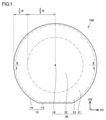
- FIG. 1 is a schematic plan view showing the configuration of the silicon carbide epitaxial substrate according to the present embodiment.
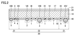
- FIG. 2 is a schematic cross-sectional view taken along the line II-II of FIG.
- FIG. 3 is an enlarged schematic view of region III of FIG.
- FIG. 4 is an enlarged schematic view of region IV of FIG.
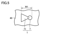
- FIG. 5 is a schematic plan view of region IV of FIG.
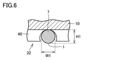
- FIG. 6 is an enlarged schematic view of the region VI of FIG.
- FIG. 7 is an enlarged schematic view of the region VII of FIG.
- FIG. 8 is an enlarged schematic view of the region VIII of FIG.
- FIG. 9 is an enlarged schematic view of the region IX of FIG.
- FIG. 10 is an enlarged schematic view of the region X of FIG. FIG.
- FIG. 11 is a schematic plan view of the region X of FIG.
- FIG. 12 is an enlarged schematic view of the region XII of FIG.
- FIG. 13 is an enlarged schematic view of the region XIII of FIG.
- FIG. 14 is an enlarged schematic view of the region XIV of FIG.
- FIG. 15 is a schematic cross-sectional view showing the configuration of a susceptor used in the method for manufacturing a silicon carbide epitaxial substrate according to the present embodiment.
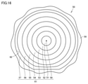
- FIG. 16 is a schematic plan view showing the configuration of a susceptor used in the method for manufacturing a silicon carbide epitaxial substrate according to the present embodiment.
- FIG. 17 is a schematic cross-sectional view showing a state in which the silicon carbide substrate is placed on the susceptor.
- An object of the present disclosure is to provide a silicon carbide epitaxial substrate capable of suppressing adsorption defects.
- defects of this disclosure According to the present disclosure, it is possible to provide a silicon carbide epitaxial substrate capable of suppressing adsorption defects.
- the silicon carbide epitaxial substrate 100 includes a silicon carbide substrate 10, a silicon carbide epitaxial layer 20, and a back surface 30.
- the silicon carbide epitaxial layer 20 is on the silicon carbide substrate 10.
- the back surface 30 is opposite to the silicon carbide epitaxial layer 20 with respect to the silicon carbide substrate 10.
- the back surface 30 includes a central region 32 having a radius of 2/3 of the radius of the back surface 30 and surrounded by a circle centered on the center 16 of the back surface 30, and an outer peripheral region 31 surrounding the central region 32.
- the surface density of the first protrusion 1 in the central region 32 is Xa
- the surface density of the second protrusion 2 in the central region 32 is Xb
- the surface density of the third protrusion 3 in the central region 32 is Xc.
- the surface density of the fourth protrusion 4 in the outer peripheral region 31 is Ya
- the surface density of the fifth protrusion 5 in the outer peripheral region 31 is Yb
- the surface density of the sixth protrusion 6 in the outer peripheral region 31 is Yc.
- the area of each of the first protruding portion 1 and the fourth protruding portion 4 is less than 100 [mu] m 2 or more 1000 .mu.m 2
- second protruding portions 2 and the fifth protruding portion each area of 5 is less than 1000 .mu.m 2 or more 5000 .mu.m 2
- each of the area of the third protrusions 3 and the sixth protrusion 6 is 5000 .mu.m 2 or more.
- the diameter of the back surface 30 is 100 mm or more, the value obtained by dividing Xa by (Xa + Ya) is 0.3 or more and 0.5 or less, Xc is 10.0 pieces / cm 2 or less, and Yc is 12.0. Pieces / cm 2 or less.
- the area of each of the first protrusion 1 and the fourth protrusion 4 is 100 ⁇ m 2 or more and less than 1000 ⁇ m 2. It means that the area of each of the plurality of first protrusions 1 is 100 ⁇ m 2 or more and less than 1000 ⁇ m 2 , and the area of each of the plurality of fourth protrusions 4 is 100 ⁇ m 2 or more and less than 1000 ⁇ m 2.
- the area of each of the second protrusions 2 and the fifth protruding portion 5 is less than 1000 .mu.m 2 or more 5000 .mu.m 2 is means that area of the plurality of second respective projections 2 is less than 1000 .mu.m 2 or more 5000 .mu.m 2, and the area of each of the plurality of fifth projections 5 is smaller than 1000 .mu.m 2 or more 5000 .mu.m 2.
- the area of each of the third protrusion 3 and the sixth protrusion 6 is 5000 ⁇ m 2 or more. It means that the area of each of the third protrusions 3 is 5000 ⁇ m 2 or more, and the area of each of the plurality of sixth protrusions 6 is 5000 ⁇ m 2 or more.
- Yb may be 30.0 pieces / cm 2 or less.
- Xc may be 3.0 pieces / cm 2 or less.
- Xb may be 20.0 pieces / cm 2 or less.
- Yc may be 4.0 pieces / cm 2 or less.
- the third protrusion 3 and the sixth protrusion 6 may contain polycrystalline silicon carbide.
- the second protrusion 2 and the fifth protrusion 5 may contain polycrystalline silicon carbide.
- the first protrusion 1 and the fourth protrusion 4 may contain polycrystalline silicon carbide.
- the value obtained by dividing Xa by (Xa + Ya) may be 0.4 or less.
- FIG. 1 is a schematic plan view showing the configuration of the silicon carbide epitaxial substrate 100 according to the present embodiment.
- FIG. 2 is a schematic cross-sectional view taken along the line II-II of FIG.
- the silicon carbide epitaxial substrate 100 according to the present embodiment includes a silicon carbide substrate 10, a first silicon carbide epitaxial layer 20, a second silicon carbide epitaxial layer 40, and an outer peripheral edge 15. And have.
- the silicon carbide substrate 10 has a first main surface 17 and a second main surface 18.
- the second main surface 18 is on the opposite side of the first main surface 17.
- the first silicon carbide epitaxial layer 20 is on the silicon carbide substrate 10.
- the first silicon carbide epitaxial layer 20 is in contact with the silicon carbide substrate 10 on the first main surface 17.
- the first main surface 17 is a boundary surface between the silicon carbide substrate 10 and the first silicon carbide epitaxial layer 20.
- the first silicon carbide epitaxial layer 20 constitutes the surface (third main surface 21) of the silicon carbide epitaxial substrate 100.
- a silicon carbide semiconductor device (not shown) is manufactured using the silicon carbide epitaxial substrate 100, a drift region (not shown), a base region (not shown), and a source region (not shown) are placed on the third main surface 21.
- a gate electrode (not shown) or a gate insulating film (not shown) is formed.
- the second silicon carbide epitaxial layer 40 is in contact with the silicon carbide substrate 10 on the second main surface 18.
- the silicon carbide epitaxial substrate 100 has a back surface 30.
- the back surface 30 is opposite to the silicon carbide epitaxial layer 20 with respect to the silicon carbide substrate 10.
- the second silicon carbide epitaxial layer 40 constitutes a part of the back surface 30 of the silicon carbide epitaxial substrate 100.
- the silicon carbide substrate 10 is located between the first silicon carbide epitaxial layer 20 and the second silicon carbide epitaxial layer 40.
- the back surface 30 includes a central region 32, an outer peripheral region 31, and an edge region 33.
- the central region 32 is a region surrounded by a circle having a radius of 2/3 of the radius R of the back surface 30 and a center 16 of the back surface 30.
- the outer peripheral region 31 surrounds the central region 32.
- the outer peripheral region 31 is a ring-shaped region when viewed in a direction perpendicular to the first main surface 17 (in other words, when viewed in the thickness direction of the silicon carbide substrate 10).
- the radius of the outer circumference of the central region 32 (the boundary between the outer peripheral region 31 and the central region 32) is 2/3 of the radius R of the back surface 30.
- the edge region 33 is a region within 3 mm from the outer peripheral edge 15 toward the center 16 of the back surface 30.
- the outer peripheral region 31 is a region sandwiched between the central region 32 and the edge region 33.
- the outer peripheral edge 15 has, for example, an orientation flat 13 and an arcuate portion 14.
- the orientation flat 13 extends along the first direction 101. As shown in FIG. 1, the orientation flat 13 is linear when viewed in a direction perpendicular to the first main surface 17.
- the arcuate portion 14 is connected to the orientation flat 13.
- the arcuate portion 14 has an arcuate shape when viewed in a direction perpendicular to the first main surface 17.
- the center 16 of the back surface 30 is located at the center of the circle including the arcuate portion 14 when viewed in a direction perpendicular to the first main surface 17.
- the back surface 30 when viewed in a direction perpendicular to the first main surface 17, the back surface 30 extends along each of the first direction 101 and the second direction 102.
- the first direction 101 is a direction perpendicular to the second direction 102.
- the first direction 101 is, for example, the ⁇ 11-20> direction.
- the first direction 101 may be, for example, the [11-20] direction.
- the first direction 101 may be a direction in which the ⁇ 11-20> direction is projected onto the first main surface 17. From another point of view, the first direction 101 may be a direction including, for example, a ⁇ 11-20> direction component.
- the second direction 102 is, for example, the ⁇ 1-100> direction.
- the second direction 102 may be, for example, the [1-100] direction.
- the second direction 102 may be, for example, a direction in which the ⁇ 1-100> direction is projected onto the first main surface 17. From another point of view, the second direction 102 may be a direction containing, for example, a ⁇ 1-100> direction component.
- the first main surface 17 may be a ⁇ 0001 ⁇ surface or a surface inclined with respect to the ⁇ 0001 ⁇ surface.
- the inclination angle (off angle) with respect to the ⁇ 0001 ⁇ surface is, for example, 2 ° or more and 6 ° or less.
- the inclination direction (off direction) of the first main surface 17 is, for example, the ⁇ 11-20> direction.
- the diameter (maximum diameter) of the back surface 30 is 100 mm (4 inches) or more.
- the diameter of the back surface 30 may be 125 mm (5 inches) or more, or 150 mm (6 inches) or more.
- the upper limit of the diameter of the back surface 30 is not particularly limited, but may be, for example, 200 mm (8 inches) or less.
- the diameter (maximum diameter) of the back surface 30 is the longest linear distance between two different points on the outer peripheral edge 15.
- the diameter of the back surface 30 may be the diameter of the outer peripheral edge 15 (that is, the arcuate portion 14) excluding the orientation flat 13.
- 4 inches means 100 mm or 101.6 mm (4 inches x 25.4 mm / inch).
- 5 inches means 125 mm or 127.0 mm (5 inches x 25.4 mm / inch).
- 6 inches means 150 mm or 152.4 mm (6 inches x 25.4 mm / inch).
- 8 inches means 200 mm or 203.2 mm (8 inches x 25.4 mm / inch).
- the polytype of silicon carbide constituting the silicon carbide substrate 10 is, for example, 4H.
- the polytype of silicon carbide constituting the first silicon carbide epitaxial layer 20 is, for example, 4H.
- the polytype of silicon carbide constituting the second silicon carbide epitaxial layer 40 is, for example, 4H.
- the thickness of the silicon carbide substrate 10 is, for example, 350 ⁇ m or more and 500 ⁇ m or less.
- the thickness of the first silicon carbide epitaxial layer 20 may be smaller than the thickness of the silicon carbide substrate 10.
- the thickness of the second silicon carbide epitaxial layer 40 may be smaller than the thickness of the silicon carbide substrate 10.
- the silicon carbide substrate 10 contains n-type impurities such as nitrogen (N).
- the conductive type of the silicon carbide substrate 10 is, for example, n type.
- the first silicon carbide epitaxial layer 20 contains n-type impurities such as nitrogen.
- the conductive type of the first silicon carbide epitaxial layer 20 is, for example, n type.
- the concentration of the n-type impurities contained in the first silicon carbide epitaxial layer 20 may be lower than the concentration of the n-type impurities contained in the silicon carbide substrate 10.
- the second silicon carbide epitaxial layer 40 contains n-type impurities such as nitrogen.
- the conductive type of the second silicon carbide epitaxial layer 40 is, for example, n type.
- the concentration of the n-type impurities contained in the second silicon carbide epitaxial layer 40 may be lower than the concentration of the n-type impurities contained in the silicon carbide substrate 10.
- the silicon carbide epitaxial substrate 100 includes, for example, a first protrusion 1, a second protrusion 2, a third protrusion 3, a fourth protrusion 4, and a fifth protrusion 5. And a sixth protrusion 6.
- the first protrusion 1 is in the central region 32.
- the second protrusion 2 is in the central region 32.
- the third protrusion 3 is in the central region 32.
- the fourth protrusion 4 is in the outer peripheral region 31.
- the fifth protrusion 5 is in the outer peripheral region 31.
- the sixth protrusion 6 is in the outer peripheral region 31.
- FIG. 3 is an enlarged schematic view of region III of FIG.
- the silicon carbide epitaxial substrate 100 has the first particle 7.
- the first particle 7 may be in contact with the silicon carbide substrate 10 on the second main surface 18.
- the second silicon carbide epitaxial layer 40 may cover the first particles 7.
- the first particle 7 may be sandwiched between the silicon carbide substrate 10 and the second silicon carbide epitaxial layer 40.
- the first particle 7 is, for example, a downfall.
- the first particle 7 may contain a silicon carbide polycrystal.
- the first particle 7 may contain carbon.
- the height of the first particle 7 (first height H1) is, for example, 1 ⁇ m or more and less than 40 ⁇ m.
- the first protrusion 1 may be composed of the second silicon carbide epitaxial layer 40.
- the first protrusion 1 may be formed on the surface of the second silicon carbide epitaxial layer 40 facing the first particles 7. Viewed in the thickness direction of the silicon carbide substrate 10, the area of the first protrusion 1 is less than 100 [mu] m 2 or more 1000 .mu.m 2.
- the area of the first protrusion 1 is the area of each of the plurality of first protrusions 1.
- the maximum width of the first protrusion 1 (first maximum width W1) is, for example, 11 ⁇ m or more and less than 36 ⁇ m.
- the first protrusion 1 constitutes a part of the central region 32.
- the maximum width of the protrusion is the longest straight line distance between two different points on the outer circumference of the protrusion when the protrusion is viewed in a direction perpendicular to the second main surface 18.
- FIG. 4 is an enlarged schematic view of region IV of FIG.
- the first protrusion 1 may have a first particle 7 and a first defect 71.
- the first defect 71 is a defect that grows in the step flow direction according to epitaxial growth starting from the first particle 7.
- the first defect 71 is continuous with the first particle 7.
- the first defect 71 is, for example, a stacking defect.
- the first defect 71 may be a triangular defect.
- the first defect 71 may be exposed on the surface of the second silicon carbide epitaxial layer 40.
- FIG. 5 is a schematic plan view of region IV of FIG.
- the shape of the first defect 71 is, for example, a triangle when viewed in the thickness direction of the silicon carbide substrate 10.
- one of the vertices of the triangle overlaps with the first particle 7.
- the distance between the two sides of the triangle may increase as the distance from the first particle 7 increases.
- the area of the first protrusion 1 is the first particle 7 and the first particle 7 from the total area of the circular first particle 7 and the triangular first defect 71. The value is obtained by subtracting the area of the overlapping portion with the defect 71.
- FIG. 6 is an enlarged schematic view of the region VI of FIG.
- the first protrusion 1 may be, for example, a downfall.
- the first protrusion 1 may contain a silicon carbide polycrystal.
- the first protrusion 1 may contain carbon.
- the first protrusion 1 may be composed of the first particles 7.
- the first protrusion 1 may be in contact with the silicon carbide substrate 10 on the second main surface 18.
- the second silicon carbide epitaxial layer 40 may surround a part of the side surface of the first protrusion 1.
- FIG. 7 is an enlarged schematic view of the region VII of FIG.
- the second protrusion 2 is, for example, a downfall.
- the second protrusion 2 may contain a silicon carbide polycrystal.
- the second protrusion 2 may contain carbon.
- the second protrusion 2 may be in contact with the silicon carbide substrate 10 on the second main surface 18.
- the second silicon carbide epitaxial layer 40 may surround a part of the side surface of the second protrusion 2.
- the height of the second protrusion 2 (second height H2) is, for example, 20 ⁇ m or more and less than 100 ⁇ m.
- the second height H2 may be larger than the first height H1.
- the second protrusion 2 is exposed from the second silicon carbide epitaxial layer 40.
- the side surface of the second protrusion 2 may be separated from the second silicon carbide epitaxial layer 40 or may be in contact with the second silicon carbide epitaxial layer 40.
- an area of the second protrusions 2 is less than 1000 .mu.m 2 or more 5000 .mu.m 2.
- the area of the second protrusion 2 is the area of each of the plurality of second protrusions 2.
- the maximum width of the second protrusion 2 (second maximum width W2) is, for example, 36 ⁇ m or more and less than 80 ⁇ m.
- the second protrusion 2 constitutes a part of the central region 32.
- the second maximum width W2 may be larger than the first maximum width W1.
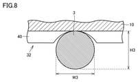
- FIG. 8 is an enlarged schematic view of the region VIII of FIG.
- the third protrusion 3 is, for example, a downfall.
- the third protrusion 3 may contain a silicon carbide polycrystal.
- the third protrusion 3 may contain carbon.
- the third protrusion 3 may be in contact with the silicon carbide substrate 10 on the second main surface 18.
- the second silicon carbide epitaxial layer 40 may surround a part of the side surface of the third protrusion 3.
- the height of the third protrusion 3 (third height H3) is, for example, 60 ⁇ m or more.
- the third height H3 may be larger than the second height H2.
- the third protrusion 3 is exposed from the second silicon carbide epitaxial layer 40.
- the side surface of the third protrusion 3 may be separated from the second silicon carbide epitaxial layer 40 or may be in contact with the second silicon carbide epitaxial layer 40.
- the area of the third protrusion 3 is 5000 ⁇ m 2 or more when viewed in the thickness direction of the silicon carbide substrate 10.
- the area of the third protrusion 3 is the area of each of the plurality of third protrusions 3.
- the maximum width of the third protrusion 3 (third maximum width W3) is, for example, 80 ⁇ m or more.
- the third protrusion 3 constitutes a part of the central region 32.
- the third maximum width W3 may be larger than the second maximum width W2.
- FIG. 9 is an enlarged schematic view of the region IX of FIG.
- the silicon carbide epitaxial substrate 100 has the second particle 8.
- the second particle 8 may be in contact with the silicon carbide substrate 10 on the second main surface 18.
- the second silicon carbide epitaxial layer 40 covers the second particles 8.
- the second particle 8 is sandwiched between the silicon carbide substrate 10 and the second silicon carbide epitaxial layer 40.
- the second particle 8 is, for example, a downfall.
- the second particle 8 may contain a silicon carbide polycrystal.
- the second particle 8 may contain carbon.
- the height of the second particle 8 (fourth height H4) is, for example, 1 ⁇ m or more and less than 40 ⁇ m.
- the fourth protrusion 4 may be composed of the second silicon carbide epitaxial layer 40.
- the fourth protrusion 4 may be formed on the surface of the second silicon carbide epitaxial layer 40 facing the second particle 8. Viewed in the thickness direction of the silicon carbide substrate 10, the area of the fourth protruding portion 4 is less than 100 [mu] m 2 or more 1000 .mu.m 2.
- the area of the fourth protrusion 4 is the area of each of the plurality of fourth protrusions 4.
- the maximum width of the fourth protrusion 4 (fourth maximum width W4) is, for example, 11 ⁇ m or more and less than 36 ⁇ m.
- the fourth protrusion 4 constitutes a part of the outer peripheral region 31.
- FIG. 10 is an enlarged schematic view of the region X in FIG.
- the fourth protrusion 4 may have a second particle 8 and a second defect 72.
- the second defect 72 is a defect that grows in the step flow direction according to epitaxial growth starting from the second particle 8.
- the second defect 72 is continuous with the second particle 8.
- the second defect 72 is, for example, a stacking defect.
- the second defect 72 may be a triangular defect.
- the second defect 72 may be exposed on the surface of the second silicon carbide epitaxial layer 40.
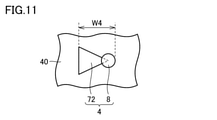
- FIG. 11 is a schematic plan view of the region X in FIG.
- the shape of the second defect 72 when viewed in the thickness direction of the silicon carbide substrate 10 is, for example, a triangle.
- one of the vertices of the triangle overlaps with the second particle 8.
- the distance between the two sides of the triangle may increase as the distance from the second particle 8 increases.
- the area of the fourth protrusion 4 is the second particle 8 and the second particle 8 from the total area of the circular second particle 8 and the triangular second defect 72. It is a value obtained by subtracting the area of the overlapping portion with the defect 72.
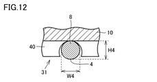
- FIG. 12 is an enlarged schematic view of the region XII of FIG.
- the fourth protrusion 4 may be, for example, a downfall.
- the fourth protrusion 4 may contain a silicon carbide polycrystal.
- the fourth protrusion 4 may contain carbon.
- the fourth protrusion 4 may be composed of the second particle 8.
- the fourth protrusion 4 may be in contact with the silicon carbide substrate 10 on the second main surface 18.
- the second silicon carbide epitaxial layer 40 may surround a part of the side surface of the fourth protrusion 4.
- FIG. 13 is an enlarged schematic view of the region XIII of FIG.
- the fifth protrusion 5 is, for example, a downfall.
- the fifth protrusion 5 may contain a silicon carbide polycrystal.
- the fifth protrusion 5 may contain carbon.
- the fifth protrusion 5 may be in contact with the silicon carbide substrate 10 on the second main surface 18.
- the second silicon carbide epitaxial layer 40 may surround a part of the side surface of the fifth protrusion 5.
- the height of the fifth protrusion 5 (fifth height H5) is, for example, 20 ⁇ m or more and less than 100 ⁇ m.
- the fifth height H5 may be larger than the fourth height H4.
- the fifth protrusion 5 is exposed from the second silicon carbide epitaxial layer 40.
- the side surface of the fifth protrusion 5 may be separated from the second silicon carbide epitaxial layer 40 or may be in contact with the second silicon carbide epitaxial layer 40.
- the area of the fifth protrusion 5 is less than 1000 .mu.m 2 or more 5000 .mu.m 2.
- the area of the fifth protrusion 5 is the area of each of the plurality of fifth protrusions 5.
- the maximum width of the fifth protrusion 5 (fifth maximum width W5) is, for example, 36 ⁇ m or more and less than 80 ⁇ m.
- the fifth protrusion 5 constitutes a part of the outer peripheral region 31.
- the fifth maximum width W5 may be larger than the fourth maximum width W4.
- FIG. 14 is an enlarged schematic view of the region XIV of FIG.
- the sixth protrusion 6 is, for example, a downfall.
- the sixth protrusion 6 may contain a silicon carbide polycrystal.
- the sixth protrusion 6 may contain carbon.
- the sixth protrusion 6 may be in contact with the silicon carbide substrate 10 on the second main surface 18.
- the second silicon carbide epitaxial layer 40 may surround a part of the side surface of the sixth protrusion 6.
- the height of the sixth protrusion 6 (sixth height H6) is, for example, 60 ⁇ m or more.
- the sixth height H6 may be larger than the fifth height H5.
- the sixth protrusion 6 is exposed from the second silicon carbide epitaxial layer 40.
- the side surface of the sixth protrusion 6 may be separated from the second silicon carbide epitaxial layer 40 or may be in contact with the second silicon carbide epitaxial layer 40.
- the area of the sixth protrusion 6 is 5000 ⁇ m 2 or more when viewed in the thickness direction of the silicon carbide substrate 10.
- the area of the sixth protrusion 6 is the area of each of the plurality of sixth protrusions 6.
- the maximum width of the sixth protrusion 6 (sixth maximum width W6) is, for example, 80 ⁇ m or more.
- the sixth protrusion 6 constitutes a part of the outer peripheral region 31.
- the sixth maximum width W6 may be larger than the fifth maximum width W5.
- the surface density of the first protrusion 1 in the central region 32 is Xa
- the surface density of the second protrusion 2 in the central region 32 is Xb
- the central region The surface density of the third protrusion 3 in 32 is Xc
- the surface density of the fourth protrusion 4 in the outer peripheral region 31 is Ya
- the surface density of the fifth protrusion 5 in the outer peripheral region 31 is Yb.
- the surface density of the sixth protrusion 6 in the region 31 is Yc
- the value obtained by dividing Xa by (Xa + Ya) is 0.3 or more and 0.5 or less
- Xc is 10.0 pieces / cm 2 or less. Yes
- Yc is 12.0 pieces / cm 2 or less.
- Yb may be, for example, 30.0 pieces / cm 2 or less.
- Yb may be, for example, 20.0 pieces / cm 2 or less, or 10.0 pieces / cm 2 or less.
- the lower limit of Yb is not particularly limited , but may be, for example, 0.1 pieces / cm 2 or more, or 0.5 pieces / cm 2 or more.
- Xc may be, for example, 3.0 pieces / cm 2 or less.
- Xc may be, for example, 2.0 pieces / cm 2 or less, or 1.0 piece / cm 2 or less.
- the lower limit of Xc is not particularly limited , but may be, for example, 0.01 pieces / cm 2 or more, or 0.05 pieces / cm 2 or more.
- the number of Xb may be, for example, 20.0 pieces / cm 2 or less.
- Xb may be, for example, 16.0 pieces / cm 2 or less, or 8.0 pieces / cm 2 or less.
- the lower limit of Xb is not particularly limited , but may be, for example, 0.1 pieces / cm 2 or more, or 0.5 pieces / cm 2 or more.
- Yc may be 4.0 pieces / cm 2 or less.
- Yc may be, for example, 3.0 pieces / cm 2 or less, or 2.0 pieces / cm 2 or less.
- the lower limit of Yc is not particularly limited , but may be, for example, 0.01 pieces / cm 2 or more, or 0.05 pieces / cm 2 or more.
- the number of Xa may be, for example, 800.0 pieces / cm 2 or less, or 400.0 pieces / cm 2 or less.
- the lower limit of Xa is not particularly limited , but may be, for example, 0.1 pieces / cm 2 or more, or 1 piece / cm 2 or more.
- Ya may be, for example, 600.0 pieces / cm 2 or less, or 400.0 pieces / cm 2 or less.
- the lower limit of Ya is not particularly limited , but may be, for example, 0.1 pieces / cm 2 or more, or 1 piece / cm 2 or more.
- the value obtained by dividing Xa by (Xa + Ya) may be 0.45 or less, or may be 0.4 or less.
- the protrusion can be identified by observing the back surface 30 of the silicon carbide epitaxial substrate 100, for example, using a defect inspection device equipped with a confocal differential interference microscope.
- a defect inspection device provided with a confocal differential interference microscope for example, a WASAVI series "SICA 6X” manufactured by Lasertec Co., Ltd. can be used.
- the magnification of the objective lens is, for example, 10 times.
- the protrusion is detected as a defect by SICA.
- the area of the detected defect is the area of the protrusion. If there is a triangular defect connected to the protrusion, the area of the triangular defect is also included.
- the measurement sensitivity of SICA is adjusted in advance so that the protrusion can be detected.
- the protrusion is defined in consideration of the typical planar shape and dimensions of the protrusion.
- the protrusions are identified based on the observed image. "Thresh S", which is an index of SICA's measurement sensitivity, is set to 40, for example.
- a confocal differential interference contrast microscope image of the entire back surface 30 is taken.
- the first protrusion 1, the second protrusion 2, the third protrusion 3, the fourth protrusion 4, the fifth protrusion 5, and the sixth protrusion 6 are observed. ..
- the number of each of the first protrusion 1, the second protrusion 2, the third protrusion 3, the fourth protrusion 4, the fifth protrusion 5, and the sixth protrusion 6. Is required.
- the value obtained by dividing the number of the first protrusion 1, the second protrusion 2, and the third protrusion 3 by the measured area in the central region 32 is the value obtained by dividing the number of the first protrusion 1, the second protrusion 2, and the third protrusion 3, respectively. It is the surface density of the part 3.
- the value obtained by dividing the number of the fourth protrusion 4, the fifth protrusion 5, and the sixth protrusion 6 by the measured area in the outer peripheral region 31 is the value obtained by dividing the number of the fourth protrusion 4, the fifth protrusion 5, and the sixth protrusion 6, respectively. It is the surface density of the part 6.
- the edge region 33 within 3 mm from the outer peripheral edge 15 is excluded from the measurement region of the protrusion (edge exclusion).
- FIG. 15 is a schematic cross-sectional view showing the configuration of a susceptor used in the method for manufacturing the silicon carbide epitaxial substrate 100 according to the present embodiment.
- FIG. 16 is a schematic plan view showing the configuration of a susceptor used in the method for manufacturing the silicon carbide epitaxial substrate 100 according to the present embodiment.
- the material constituting the susceptor is, for example, silicon carbide.
- the susceptor 50 is provided with a silicon carbide substrate accommodating portion 60.
- the silicon carbide substrate accommodating portion 60 is composed of a side surface 62 and a bottom surface 61.
- the side surface 62 is connected to the top surface 59 of the susceptor 50.
- the bottom surface 61 is connected to the side surface 62.
- a plurality of concentrically arranged recesses are formed on the bottom surface 61 of the silicon carbide substrate accommodating portion 60.
- the plurality of recesses include a first recess 51, a second recess 52, a third recess 53, a fourth recess 54, a fifth recess 55, a sixth recess 56, and a seventh recess 57. And have.
- the first recess 51 is formed so as to surround the central portion 58 of the bottom surface 61.
- the second recess 52 is formed so as to surround the first recess 51.
- the third recess 53 is formed so as to surround the second recess 52.
- the fourth recess 54 is formed so as to surround the third recess 53.
- the fifth recess 55 is formed so as to surround the fourth recess 54.
- the sixth recess 56 is formed so as to surround the fifth recess 55.
- the seventh recess 57 is formed so as to surround the sixth recess 56.
- the angle ⁇ of the tip of the protrusion is, for example, 30 ° or more and 45 ° or less.
- the height T of the protrusion is, for example, 100 ⁇ m or more.
- the silicon carbide substrate 10 is prepared.
- the sublimation method produces a polytype 4H silicon carbide single crystal.
- the silicon carbide single crystal is sliced, for example, by a wire saw.
- the silicon carbide substrate 10 contains n-type impurities such as nitrogen.
- the conductive type of the silicon carbide substrate 10 is, for example, n type.
- mechanical polishing, chemical mechanical polishing, and cleaning are performed on the silicon carbide substrate 10. From the above, the silicon carbide substrate 10 is prepared.
- FIG. 17 is a schematic cross-sectional view showing a state in which the silicon carbide substrate 10 is placed on the susceptor 50.
- the susceptor 50 on which the silicon carbide substrate 10 is placed is installed in the CVD furnace.
- Deposits such as crystal raw materials used in the previous epitaxial growth adhere to the inner wall of the CVD furnace.
- the deposits are, for example, silicon carbide particles or carbon particles.
- the inner wall of the CVD furnace is made of, for example, a carbon member.
- the carbon member constituting the inner wall is bent.
- the deposits adhering to the inner wall fall onto the susceptor 50.
- the deposits that fall on the susceptor 50 are called downfalls. Downfalls are generally particulate.
- the downfall is, for example, polycrystalline silicon carbide or carbon.
- the diameter of the down fall is, for example, in the range of 0.1 ⁇ m or more and 1 mm or less.
- the down fall falls on, for example, the top surface 59 of the down feather 50.
- the down fall that has fallen on the top surface 59 of the susceptor 50 moves to the bottom surface 61 of the silicon carbide substrate accommodating portion 60 of the susceptor 50. If the bottom surface 61 of the susceptor 50 has a down fall, the down fall adheres to the back surface 30 of the silicon carbide substrate 10 when the silicon carbide substrate 10 is arranged on the bottom surface 61 of the silicon carbide substrate accommodating portion 60.
- the downfall 9 having a large diameter enters the inside of the recesses. Since the silicon carbide substrate 10 is placed on the apex of the protrusion, it does not come into contact with the downfall 9 having a large diameter. Therefore, it is possible to prevent the downfall 9 from adhering to the back surface (second main surface 18) of the silicon carbide substrate 10. There may be a downfall with a small diameter at the apex of the protrusion. The downfall with a small diameter adheres to the back surface (second main surface 18) of the silicon carbide substrate 10.
- the back surface (second main main) of the silicon carbide substrate 10 is adjusted.
- the size of the downfall adhering to the surface 18), the surface density, and the like can be controlled.
- the step of manufacturing the silicon carbide semiconductor device using the silicon carbide epitaxial substrate 100 usually includes an exposure step and an inspection step. During these steps, the back surface 30 of the silicon carbide epitaxial substrate 100 is adsorbed on the chuck.
- a vacuum chuck, an electrostatic chuck and the like are generally used.
- poor adsorption of the silicon carbide epitaxial substrate 100 to the chuck causes poor exposure.
- the inventors obtained the following findings.
- the inventor paid attention to the size of the protrusion existing on the back surface 30 of the silicon carbide epitaxial substrate 100 and the position of the protrusion.
- six types of protrusions are focused on the area of the protrusions viewed in the direction perpendicular to the back surface 30 and the region of the back surface (central region or outer peripheral region) where the protrusions are present.
- the surface density of the first protrusion 1 in the central region 32 is Xa
- the surface density of the second protrusion 2 in the central region 32 is Xb
- the central region is Xc
- the surface density of the fourth protrusion 4 in the outer peripheral area 31 is Ya
- the surface density of the fifth protrusion 5 in the outer peripheral area 31 is Yb.
- the area of each of the first protruding portion 1 and the fourth protruding portion 4 is 100 [mu] m 2 or more 1000 .mu.m 2 less than a and the area of each of the second protrusion 2 and the fifth protruding portion 5 is less than 1000 .mu.m 2 or more 5000 .mu.m 2, and in a third each of the areas of the protrusions 3 and the sixth protrusion 6 5000 .mu.m 2 or more be.
- the diameter of the back surface 30 is 100 mm or more, the value obtained by dividing Xa by (Xa + Ya) is 0.3 or more and 0.5 or less, Xc is 10.0 pieces / cm 2 or less, and Yc is 12.0. Pieces / cm 2 or less. As a result, it is possible to suppress the adsorption failure of the silicon carbide epitaxial substrate 100.
- the value obtained by dividing Xa by (Xa + Ya) may be 0.4 or less. Thereby, the adsorption failure of the silicon carbide epitaxial substrate 100 can be further suppressed.
- sample preparation First, seven silicon carbide epitaxial substrates 100 having different values obtained by dividing Xa by (Xa + Ya) were prepared.
- the silicon carbide epitaxial substrate 100 of Samples 1 to 5 is an example.
- the silicon carbide epitaxial substrate 100 of the samples 6 and 7 is a comparative example.
- the value obtained by dividing Xa by (Xa + Ya) was set to 0.3 or more and 0.5 or less.
- the value obtained by dividing Xa by (Xa + Ya) was made larger than 0.5.
- Table 1 shows the evaluation results of the silicon carbide substrates 10 of Samples 1 to 7.
- the evaluation result was set to "A”.
- the evaluation result was set to "B”.
- the evaluation result was set to "C”.
Landscapes
- Chemical & Material Sciences (AREA)
- Engineering & Computer Science (AREA)
- Materials Engineering (AREA)
- Metallurgy (AREA)
- Organic Chemistry (AREA)
- Crystallography & Structural Chemistry (AREA)
- Inorganic Chemistry (AREA)
- General Chemical & Material Sciences (AREA)
- Chemical Kinetics & Catalysis (AREA)
- Mechanical Engineering (AREA)
- Crystals, And After-Treatments Of Crystals (AREA)
Abstract
中央領域にある第1突起部の面密度をXaとし、中央領域にある第2突起部の面密度をXbとし、中央領域にある第3突起部の面密度をXcとし、外周領域にある第4突起部の面密度をYaとし、外周領域にある第5突起部の面密度をYbとし、外周領域にある第6突起部の面密度をYcとした場合、炭化珪素基板の厚み方向に見て、第1突起部および第4突起部の各々の面積は100μm2以上1000μm2未満であり、第2突起部および第5突起部の各々の面積は1000μm2以上5000μm2未満であり、かつ第3突起部および第6突起部の各々の面積は5000μm2以上である。裏面の直径は100mm以上であり、Xaを(Xa+Ya)で除した値は0.3以上0.5以下であり、Xcは10.0個/cm2以下である、かつYcは12.0個/cm2以下である。
Description
本開示は、炭化珪素エピタキシャル基板に関する。本出願は、2020年7月22日に出願した日本特許出願である特願2020-125075号に基づく優先権を主張する。当該日本特許出願に記載された全ての記載内容は、参照によって本明細書に援用される。
特開2019-46855号公報(特許文献1)には、CVD(Chemical Vapor Deposition)を用いて、炭化珪素エピタキシャル膜を形成する方法が記載されている。
本開示に係る炭化珪素エピタキシャル基板は、炭化珪素基板と、炭化珪素エピタキシャル層と、裏面とを備えている。炭化珪素エピタキシャル層は、炭化珪素基板上にある。裏面は、炭化珪素基板に対して炭化珪素エピタキシャル層の反対にある。裏面は、裏面の半径の2/3を半径としかつ裏面の中心を中心とする円に取り囲まれた中央領域と、中央領域を取り囲む外周領域とを含む。中央領域にある第1突起部の面密度をXaとし、中央領域にある第2突起部の面密度をXbとし、中央領域にある第3突起部の面密度をXcとし、外周領域にある第4突起部の面密度をYaとし、外周領域にある第5突起部の面密度をYbとし、外周領域にある第6突起部の面密度をYcとした場合、炭化珪素基板の厚み方向に見て、第1突起部および第4突起部の各々の面積は100μm2以上1000μm2未満であり、第2突起部および第5突起部の各々の面積は1000μm2以上5000μm2未満であり、かつ第3突起部および第6突起部の各々の面積は5000μm2以上である。裏面の直径は100mm以上であり、Xaを(Xa+Ya)で除した値は0.3以上0.5以下であり、Xcは10.0個/cm2以下である、かつYcは12.0個/cm2以下である。
[本開示が解決しようとする課題]
本開示の目的は、吸着不良を抑制可能な炭化珪素エピタキシャル基板を提供することである。
[本開示の効果]
本開示によれば、吸着不良を抑制可能な炭化珪素エピタキシャル基板を提供することができる。
本開示の目的は、吸着不良を抑制可能な炭化珪素エピタキシャル基板を提供することである。
[本開示の効果]
本開示によれば、吸着不良を抑制可能な炭化珪素エピタキシャル基板を提供することができる。
[本開示の実施形態の概要]
まず本開示の実施形態の概要について説明する。本明細書の結晶学的記載においては、個別方位を[]、集合方位を<>、個別面を()、集合面を{}でそれぞれ示す。結晶学上の指数が負であることは、通常、数字の上に”-”(バー)を付すことによって表現されるが、本明細書では数字の前に負の符号を付すことによって結晶学上の負の指数を表現する。
まず本開示の実施形態の概要について説明する。本明細書の結晶学的記載においては、個別方位を[]、集合方位を<>、個別面を()、集合面を{}でそれぞれ示す。結晶学上の指数が負であることは、通常、数字の上に”-”(バー)を付すことによって表現されるが、本明細書では数字の前に負の符号を付すことによって結晶学上の負の指数を表現する。
(1)本開示に係る炭化珪素エピタキシャル基板100は、炭化珪素基板10と、炭化珪素エピタキシャル層20と、裏面30とを備えている。炭化珪素エピタキシャル層20は、炭化珪素基板10上にある。裏面30は、炭化珪素基板10に対して炭化珪素エピタキシャル層20の反対にある。裏面30は、裏面30の半径の2/3を半径としかつ裏面30の中心16を中心とする円に取り囲まれた中央領域32と、中央領域32を取り囲む外周領域31とを含む。中央領域32にある第1突起部1の面密度をXaとし、中央領域32にある第2突起部2の面密度をXbとし、中央領域32にある第3突起部3の面密度をXcとし、外周領域31にある第4突起部4の面密度をYaとし、外周領域31にある第5突起部5の面密度をYbとし、外周領域31にある第6突起部6の面密度をYcとした場合、炭化珪素基板10の厚み方向に見て、第1突起部1および第4突起部4の各々の面積は100μm2以上1000μm2未満であり、第2突起部2および第5突起部5の各々の面積は1000μm2以上5000μm2未満であり、かつ第3突起部3および第6突起部6の各々の面積は5000μm2以上である。裏面30の直径は100mm以上であり、Xaを(Xa+Ya)で除した値は0.3以上0.5以下であり、Xcは10.0個/cm2以下である、かつYcは12.0個/cm2以下である。
なお、第1突起部1が複数でありかつ第4突起部4が複数である場合、第1突起部1および第4突起部4の各々の面積が100μm2以上1000μm2未満であるとは、複数の第1突起部1の各々の面積が100μm2以上1000μm2未満であり、かつ複数の第4突起部4の各々の面積が100μm2以上1000μm2未満であることを意味する。同様に、第2突起部2が複数でありかつ第5突起部5が複数である場合、第2突起部2および第5突起部5の各々の面積は1000μm2以上5000μm2未満であるとは、複数の第2突起部2の各々の面積が1000μm2以上5000μm2未満であり、かつ複数の第5突起部5の各々の面積が1000μm2以上5000μm2未満であることを意味する。同様に、第3突起部3が複数でありかつ第6突起部6が複数である場合、第3突起部3および第6突起部6の各々の面積は5000μm2以上であるとは、複数の第3突起部3の各々の面積が5000μm2以上であり、かつ複数の第6突起部6の各々の面積が5000μm2以上であることを意味する。
(2)上記(1)に係る炭化珪素エピタキシャル基板100によれば、Ybは30.0個/cm2以下であってもよい。
(3)上記(1)または(2)に係る炭化珪素エピタキシャル基板100によれば、Xcは3.0個/cm2以下であってもよい。
(4)上記(1)から(3)のいずれかに係る炭化珪素エピタキシャル基板100によれば、Xbは20.0個/cm2以下であってもよい。
(5)上記(1)から(4)のいずれかに係る炭化珪素エピタキシャル基板100によれば、Ycは4.0個/cm2以下であってもよい。
(6)上記(1)から(5)のいずれかに係る炭化珪素エピタキシャル基板100によれば、第3突起部3および第6突起部6は、多結晶炭化珪素を含んでいてもよい。
(7)上記(1)から(6)のいずれかに係る炭化珪素エピタキシャル基板100によれば、第2突起部2および第5突起部5は、多結晶炭化珪素を含んでいてもよい。
(8)上記(1)から(7)のいずれかに係る炭化珪素エピタキシャル基板100によれば、第1突起部1および第4突起部4は、多結晶炭化珪素を含んでいてもよい。
(9)上記(1)から(8)のいずれかに係る炭化珪素エピタキシャル基板100によれば、Xaを(Xa+Ya)で除した値は0.4以下であってもよい。
[本開示の実施形態の詳細]
以下、本開示の実施形態の詳細について説明する。以下の説明では、同一または対応する要素には同一の符号を付し、それらについて同じ説明は繰り返さない。
以下、本開示の実施形態の詳細について説明する。以下の説明では、同一または対応する要素には同一の符号を付し、それらについて同じ説明は繰り返さない。
(炭化珪素エピタキシャル基板)
図1は、本実施形態に係る炭化珪素エピタキシャル基板100の構成を示す平面模式図である。図2は、図1のII-II線に沿った断面模式図である。図1および図2に示されるように、本実施形態に係る炭化珪素エピタキシャル基板100は、炭化珪素基板10と、第1炭化珪素エピタキシャル層20と、第2炭化珪素エピタキシャル層40と、外周縁15とを有している。炭化珪素基板10は、第1主面17と、第2主面18とを有している。第2主面18は、第1主面17の反対側にある。
図1は、本実施形態に係る炭化珪素エピタキシャル基板100の構成を示す平面模式図である。図2は、図1のII-II線に沿った断面模式図である。図1および図2に示されるように、本実施形態に係る炭化珪素エピタキシャル基板100は、炭化珪素基板10と、第1炭化珪素エピタキシャル層20と、第2炭化珪素エピタキシャル層40と、外周縁15とを有している。炭化珪素基板10は、第1主面17と、第2主面18とを有している。第2主面18は、第1主面17の反対側にある。
第1炭化珪素エピタキシャル層20は、炭化珪素基板10上にある。第1炭化珪素エピタキシャル層20は、第1主面17において、炭化珪素基板10に接している。第1主面17は、炭化珪素基板10と、第1炭化珪素エピタキシャル層20との境界面である。第1炭化珪素エピタキシャル層20は、炭化珪素エピタキシャル基板100の表面(第3主面21)を構成する。炭化珪素エピタキシャル基板100を用いて炭化珪素半導体装置(図示せず)を製造する場合、第3主面21上にドリフト領域(図示せず)、ベース領域(図示せず)、ソース領域(図示せず)、ゲート電極(図示せず)またはゲート絶縁膜(図示せず)などが形成される。
図2に示されるように、第2炭化珪素エピタキシャル層40は、第2主面18において、炭化珪素基板10に接している。炭化珪素エピタキシャル基板100は、裏面30を有している。裏面30は、炭化珪素基板10に対して炭化珪素エピタキシャル層20の反対にある。第2炭化珪素エピタキシャル層40は、炭化珪素エピタキシャル基板100の裏面30の一部を構成する。炭化珪素基板10は、第1炭化珪素エピタキシャル層20と、第2炭化珪素エピタキシャル層40との間にある。
図1に示されるように、裏面30は、中央領域32と、外周領域31と、エッジ領域33とを含んでいる。中央領域32は、裏面30の半径Rの2/3を半径としかつ裏面30の中心16を中心とする円に取り囲まれた領域である。外周領域31は、中央領域32を取り囲んでいる。第1主面17に対して垂直な方向に見て(言い換えれば、炭化珪素基板10の厚み方向に見て)、外周領域31は、リング状の領域である。図1に示されるように、中央領域32の外周(外周領域31と中央領域32との境界)の半径は、裏面30の半径Rの2/3である。エッジ領域33は、外周縁15から裏面30の中心16に向かって3mm以内の領域である。外周領域31は、中央領域32とエッジ領域33とに挟まれた領域である。
外周縁15は、たとえばオリエンテーションフラット13と、円弧状部14とを有している。オリエンテーションフラット13は、第1方向101に沿って延在している。図1に示されるように、オリエンテーションフラット13は、第1主面17に対して垂直な方向に見て、直線状である。円弧状部14は、オリエンテーションフラット13に連なっている。円弧状部14は、第1主面17に対して垂直な方向に見て、円弧状である。裏面30の中心16は、第1主面17に対して垂直な方向に見て、円弧状部14を含む円の中心に位置している。
図1に示されるように、第1主面17に対して垂直な方向に見て、裏面30は、第1方向101および第2方向102の各々に沿って拡がっている。第1主面17に対して垂直な方向に見て、第1方向101は、第2方向102に対して垂直な方向である。
第1方向101は、たとえば<11-20>方向である。第1方向101は、たとえば[11-20]方向であってもよい。第1方向101は、<11-20>方向を第1主面17に射影した方向であってもよい。別の観点から言えば、第1方向101は、たとえば<11-20>方向成分を含む方向であってもよい。
第2方向102は、たとえば<1-100>方向である。第2方向102は、たとえば[1-100]方向であってもよい。第2方向102は、たとえば<1-100>方向を第1主面17に射影した方向であってもよい。別の観点から言えば、第2方向102は、たとえば<1-100>方向成分を含む方向であってもよい。
第1主面17は、{0001}面であってもよいし、{0001}面に対して傾斜した面であってもよい。第1主面17は、{0001}面に対して傾斜している場合、{0001}面に対する傾斜角(オフ角)は、たとえば2°以上6°以下である。第1主面17が{0001}面に対して傾斜している場合、第1主面17の傾斜方向(オフ方向)は、たとえば<11-20>方向である。
裏面30の直径(最大径)は、100mm(4インチ)以上である。裏面30の直径は、125mm(5インチ)以上でもあってもよいし、150mm(6インチ)以上でもよい。裏面30の直径の上限は、特に限定されないが、たとえば200mm(8インチ)以下であってもよい。なお裏面30の直径(最大径)は、外周縁15上の異なる2点間の最長直線距離である。裏面30の直径は、オリエンテーションフラット13を除いた外周縁15(つまり円弧状部14)の直径であってもよい。
なお本明細書において、4インチは、100mm又は101.6mm(4インチ×25.4mm/インチ)のことである。5インチは、125mm又は127.0mm(5インチ×25.4mm/インチ)のことである。6インチは、150mm又は152.4mm(6インチ×25.4mm/インチ)のことである。8インチは、200mm又は203.2mm(8インチ×25.4mm/インチ)のことである。
炭化珪素基板10を構成する炭化珪素のポリタイプは、たとえば4Hである。同様に、第1炭化珪素エピタキシャル層20を構成する炭化珪素のポリタイプは、たとえば4Hである。同様に、第2炭化珪素エピタキシャル層40を構成する炭化珪素のポリタイプは、たとえば4Hである。炭化珪素基板10の厚みは、たとえば350μm以上500μm以下である。第1炭化珪素エピタキシャル層20の厚みは、炭化珪素基板10の厚みよりも小さくてもよい。第2炭化珪素エピタキシャル層40の厚みは、炭化珪素基板10の厚みよりも小さくてもよい。
炭化珪素基板10は、たとえば窒素(N)などのn型不純物を含んでいる。炭化珪素基板10の導電型は、たとえばn型である。第1炭化珪素エピタキシャル層20は、たとえば窒素などのn型不純物を含んでいる。第1炭化珪素エピタキシャル層20の導電型は、たとえばn型である。第1炭化珪素エピタキシャル層20が含むn型不純物の濃度は、炭化珪素基板10が含むn型不純物の濃度より低くてもよい。第2炭化珪素エピタキシャル層40は、たとえば窒素などのn型不純物を含んでいる。第2炭化珪素エピタキシャル層40の導電型は、たとえばn型である。第2炭化珪素エピタキシャル層40が含むn型不純物の濃度は、炭化珪素基板10が含むn型不純物の濃度より低くてもよい。
図2に示されるように、炭化珪素エピタキシャル基板100は、たとえば、第1突起部1と、第2突起部2と、第3突起部3と、第4突起部4と、第5突起部5と、第6突起部6とを有している。第1突起部1は、中央領域32にある。第2突起部2は、中央領域32にある。第3突起部3は、中央領域32にある。第4突起部4は、外周領域31にある。第5突起部5は、外周領域31にある。第6突起部6は、外周領域31にある。
図3は、図2の領域IIIの拡大模式図である。図3に示されるように、炭化珪素エピタキシャル基板100は、第1粒子7を有している。第1粒子7は、第2主面18において、炭化珪素基板10に接していてもよい。第2炭化珪素エピタキシャル層40は、第1粒子7を覆っていてもよい。第1粒子7は、炭化珪素基板10と、第2炭化珪素エピタキシャル層40とに挟まれていてもよい。第1粒子7は、たとえばダウンフォールである。第1粒子7は、炭化珪素多結晶を含んでいてもよい。第1粒子7は、炭素を含んでいてもよい。第1粒子7の高さ(第1高さH1)は、たとえば1μm以上40μm未満である。
図3に示されるように、第1突起部1は、第2炭化珪素エピタキシャル層40により構成されていてもよい。第1突起部1は、第1粒子7に対面する第2炭化珪素エピタキシャル層40の表面に形成されていてもよい。炭化珪素基板10の厚み方向に見て、第1突起部1の面積は100μm2以上1000μm2未満である。第1突起部1が複数ある場合には、第1突起部1の面積とは、複数の第1突起部1の各々の面積である。第1突起部1の最大幅(第1最大幅W1)は、たとえば11μm以上36μm未満である。第1突起部1は、中央領域32の一部を構成する。なお、突起部の最大幅とは、第2主面18に対して垂直な方向に突起部を見た場合において、突起部の外周上の異なる2点間の最長直線距離である。
図4は、図2の領域IVの拡大模式図である。図4に示されるように、第1突起部1は、第1粒子7と、第1欠陥71とを有していてもよい。第1欠陥71は、第1粒子7を起点として、エピタキシャル成長に従ってステップフロー方向に成長した欠陥である。第1欠陥71は、第1粒子7に連なっている。第1欠陥71は、たとえば積層欠陥である。第1欠陥71は、三角欠陥であってもよい。第1欠陥71は、第2炭化珪素エピタキシャル層40の表面に露出していてもよい。
図5は、図2の領域IVの平面模式図である。図5に示されるように、炭化珪素基板10の厚み方向に見て、第1欠陥71の形状は、たとえば三角形である。炭化珪素基板10の厚み方向に見て、三角形の頂点の一つは、第1粒子7と重なっている。炭化珪素基板10の厚み方向に見て、第1粒子7から離れるにつれて、三角形の2辺の間隔は大きくなっていてもよい。炭化珪素基板10の厚み方向に見て、第1突起部1の面積は、円状の第1粒子7の面積と三角形状の第1欠陥71の面積の合計から、第1粒子7と第1欠陥71との重なり部分の面積を差し引いた値となる。
図6は、図2の領域VIの拡大模式図である。図6に示されるように、第1突起部1は、たとえばダウンフォールであってもよい。第1突起部1は、炭化珪素多結晶を含んでいてもよい。第1突起部1は、炭素を含んでいてもよい。第1突起部1は、第1粒子7により構成されていてもよい。第1突起部1は、第2主面18において、炭化珪素基板10に接していてもよい。第2炭化珪素エピタキシャル層40は、第1突起部1の側面の一部を取り囲んでいてもよい。
図7は、図2の領域VIIの拡大模式図である。図7に示されるように、第2突起部2は、たとえばダウンフォールである。第2突起部2は、炭化珪素多結晶を含んでいてもよい。第2突起部2は、炭素を含んでいてもよい。第2突起部2は、第2主面18において、炭化珪素基板10に接していてもよい。第2炭化珪素エピタキシャル層40は、第2突起部2の側面の一部を取り囲んでいてもよい。第2突起部2の高さ(第2高さH2)は、たとえば20μm以上100μm未満である。第2高さH2は、第1高さH1よりも大きくてもよい。
図7に示されるように、第2突起部2は、第2炭化珪素エピタキシャル層40から露出している。第2突起部2の側面は、第2炭化珪素エピタキシャル層40から離間していてもよいし、第2炭化珪素エピタキシャル層40に接していてもよい。炭化珪素基板10の厚み方向に見て、第2突起部2の面積は1000μm2以上5000μm2未満である。第2突起部2が複数ある場合には、第2突起部2の面積とは、複数の第2突起部2の各々の面積である。第2突起部2の最大幅(第2最大幅W2)は、たとえば36μm以上80μm未満である第2突起部2は、中央領域32の一部を構成する。第2最大幅W2は、第1最大幅W1よりも大きくてもよい。
図8は、図2の領域VIIIの拡大模式図である。図8に示されるように、第3突起部3は、たとえばダウンフォールである。第3突起部3は、炭化珪素多結晶を含んでいてもよい。第3突起部3は、炭素を含んでいてもよい。第3突起部3は、第2主面18において、炭化珪素基板10に接していてもよい。第2炭化珪素エピタキシャル層40は、第3突起部3の側面の一部を取り囲んでいてもよい。第3突起部3の高さ(第3高さH3)は、たとえば60μm以上である。第3高さH3は、第2高さH2よりも大きくてもよい。
図8に示されるように、第3突起部3は、第2炭化珪素エピタキシャル層40から露出している。第3突起部3の側面は、第2炭化珪素エピタキシャル層40から離間していてもよいし、第2炭化珪素エピタキシャル層40に接していてもよい。炭化珪素基板10の厚み方向に見て、第3突起部3の面積は5000μm2以上である。第3突起部3が複数ある場合には、第3突起部3の面積とは、複数の第3突起部3の各々の面積である。第3突起部3の最大幅(第3最大幅W3)は、たとえば80μm以上である。第3突起部3は、中央領域32の一部を構成する。第3最大幅W3は、第2最大幅W2よりも大きくてもよい。
図9は、図2の領域IXの拡大模式図である。図9に示されるように、炭化珪素エピタキシャル基板100は、第2粒子8を有している。第2粒子8は、第2主面18において、炭化珪素基板10に接していてもよい。第2炭化珪素エピタキシャル層40は、第2粒子8を覆っている。第2粒子8は、炭化珪素基板10と、第2炭化珪素エピタキシャル層40とに挟まれている。第2粒子8は、たとえばダウンフォールである。第2粒子8は、炭化珪素多結晶を含んでいてもよい。第2粒子8は、炭素を含んでいてもよい。第2粒子8の高さ(第4高さH4)は、たとえば1μm以上40μm未満である。
図9に示されるように、第4突起部4は、第2炭化珪素エピタキシャル層40により構成されていてもよい。第4突起部4は、第2粒子8に対面する第2炭化珪素エピタキシャル層40の表面に形成されていてもよい。炭化珪素基板10の厚み方向に見て、第4突起部4の面積は100μm2以上1000μm2未満である。第4突起部4が複数ある場合には、第4突起部4の面積とは、複数の第4突起部4の各々の面積である。第4突起部4の最大幅(第4最大幅W4)は、たとえば11μm以上36μm未満である。第4突起部4は、外周領域31の一部を構成する。
図10は、図2の領域Xの拡大模式図である。図10に示されるように、第4突起部4は、第2粒子8と、第2欠陥72とを有していてもよい。第2欠陥72は、第2粒子8を起点として、エピタキシャル成長に従ってステップフロー方向に成長した欠陥である。第2欠陥72は、第2粒子8に連なっている。第2欠陥72は、たとえば積層欠陥である。第2欠陥72は、三角欠陥であってもよい。第2欠陥72は、第2炭化珪素エピタキシャル層40の表面に露出していてもよい。
図11は、図2の領域Xの平面模式図である。図11に示されるように、炭化珪素基板10の厚み方向に見て、第2欠陥72の形状は、たとえば三角形である。炭化珪素基板10の厚み方向に見て、三角形の頂点の一つは、第2粒子8と重なっている。炭化珪素基板10の厚み方向に見て、第2粒子8から離れるにつれて、三角形の2辺の間隔は大きくなっていてもよい。炭化珪素基板10の厚み方向に見て、第4突起部4の面積は、円状の第2粒子8の面積と三角形状の第2欠陥72の面積の合計から、第2粒子8と第2欠陥72との重なり部分の面積を差し引いた値となる。
図12は、図2の領域XIIの拡大模式図である。図12に示されるように、第4突起部4は、たとえばダウンフォールであってもよい。第4突起部4は、炭化珪素多結晶を含んでいてもよい。第4突起部4は、炭素を含んでいてもよい。第4突起部4は、第2粒子8により構成されていてもよい。第4突起部4は、第2主面18において、炭化珪素基板10に接していてもよい。第2炭化珪素エピタキシャル層40は、第4突起部4の側面の一部を取り囲んでいてもよい。
図13は、図2の領域XIIIの拡大模式図である。図13に示されるように、第5突起部5は、たとえばダウンフォールである。第5突起部5は、炭化珪素多結晶を含んでいてもよい。第5突起部5は、炭素を含んでいてもよい。第5突起部5は、第2主面18において、炭化珪素基板10に接していてもよい。第2炭化珪素エピタキシャル層40は、第5突起部5の側面の一部を取り囲んでいてもよい。第5突起部5の高さ(第5高さH5)は、たとえば20μm以上100μm未満である。第5高さH5は、第4高さH4よりも大きくてもよい。
図13に示されるように、第5突起部5は、第2炭化珪素エピタキシャル層40から露出している。第5突起部5の側面は、第2炭化珪素エピタキシャル層40から離間していてもよいし、第2炭化珪素エピタキシャル層40に接していてもよい。炭化珪素基板10の厚み方向に見て、第5突起部5の面積は1000μm2以上5000μm2未満である。第5突起部5が複数ある場合には、第5突起部5の面積とは、複数の第5突起部5の各々の面積である。第5突起部5の最大幅(第5最大幅W5)は、たとえば36μm以上80μm未満である。第5突起部5は、外周領域31の一部を構成する。第5最大幅W5は、第4最大幅W4よりも大きくてもよい。
図14は、図2の領域XIVの拡大模式図である。図14に示されるように、第6突起部6は、たとえばダウンフォールである。第6突起部6は、炭化珪素多結晶を含んでいてもよい。第6突起部6は、炭素を含んでいてもよい。第6突起部6は、第2主面18において、炭化珪素基板10に接していてもよい。第2炭化珪素エピタキシャル層40は、第6突起部6の側面の一部を取り囲んでいてもよい。第6突起部6の高さ(第6高さH6)は、たとえば60μm以上である。第6高さH6は、第5高さH5よりも大きくてもよい。
図14に示されるように、第6突起部6は、第2炭化珪素エピタキシャル層40から露出している。第6突起部6の側面は、第2炭化珪素エピタキシャル層40から離間していてもよいし、第2炭化珪素エピタキシャル層40に接していてもよい。炭化珪素基板10の厚み方向に見て、第6突起部6の面積は5000μm2以上である。第6突起部6が複数ある場合には、第6突起部6の面積とは、複数の第6突起部6の各々の面積である。第6突起部6の最大幅(第6最大幅W6)は、たとえば80μm以上である。第6突起部6は、外周領域31の一部を構成する。第6最大幅W6は、第5最大幅W5よりも大きくてもよい。
本実施形態に係る炭化珪素エピタキシャル基板100によれば、中央領域32にある第1突起部1の面密度をXaとし、中央領域32にある第2突起部2の面密度をXbとし、中央領域32にある第3突起部3の面密度をXcとし、外周領域31にある第4突起部4の面密度をYaとし、外周領域31にある第5突起部5の面密度をYbとし、外周領域31にある第6突起部6の面密度をYcとした場合、Xaを(Xa+Ya)で除した値は0.3以上0.5以下であり、Xcは10.0個/cm2以下である、かつYcは12.0個/cm2以下である。
本実施形態に係る炭化珪素エピタキシャル基板100によれば、Ybは、たとえば30.0個/cm2以下であってもよい。Ybは、たとえば20.0個/cm2以下であってもよいし、10.0個/cm2以下であってもよい。Ybの下限は、特に限定されないが、たとえば0.1個/cm2以上であってもよいし、0.5個/cm2以上であってもよい。
本実施形態に係る炭化珪素エピタキシャル基板100によれば、Xcは、たとえば3.0個/cm2以下であってもよい。Xcは、たとえば2.0個/cm2以下であってもよい、1.0個/cm2以下であってもよい。Xcの下限は、特に限定されないが、たとえば0.01個/cm2以上であってもよいし、0.05個/cm2以上であってもよい。
本実施形態に係る炭化珪素エピタキシャル基板100によれば、Xbは、たとえば20.0個/cm2以下であってもよい。Xbは、たとえば16.0個/cm2以下であってもよいし、8.0個/cm2以下であってもよい。Xbの下限は、特に限定されないが、たとえば0.1個/cm2以上であってもよいし、0.5個/cm2以上であってもよい。
本実施形態に係る炭化珪素エピタキシャル基板100によれば、Ycは4.0個/cm2以下であってもよい。Ycは、たとえば3.0個/cm2以下であってもよい、2.0個/cm2以下であってもよい。Ycの下限は、特に限定されないが、たとえば0.01個/cm2以上であってもよいし、0.05個/cm2以上であってもよい。
本実施形態に係る炭化珪素エピタキシャル基板100によれば、Xaは、たとえば800.0個/cm2以下であってもよいし、400.0個/cm2以下であってもよい。Xaの下限は、特に限定されないが、たとえば0.1個/cm2以上であってもよいし、1個/cm2以上であってもよい。
本実施形態に係る炭化珪素エピタキシャル基板100によれば、Yaは、たとえば600.0個/cm2以下であってもよいし、400.0個/cm2以下であってもよい。Yaの下限は、特に限定されないが、たとえば0.1個/cm2以上であってもよいし、1個/cm2以上であってもよい。
本実施形態に係る炭化珪素エピタキシャル基板100によれば、Xaを(Xa+Ya)で除した値は0.45以下であってもよいし、0.4以下であってもよい。
(突起部の測定方法)
次に、突起部の測定方法について説明する。突起部は、たとえば共焦点微分干渉顕微鏡を備える欠陥検査装置を用いて、炭化珪素エピタキシャル基板100の裏面30を観察することにより特定することができる。共焦点微分干渉顕微鏡を備える欠陥検査装置としては、たとえばレーザーテック株式会社製のWASAVIシリーズ「SICA 6X」を用いることができる。対物レンズの倍率はたとえば10倍である。
次に、突起部の測定方法について説明する。突起部は、たとえば共焦点微分干渉顕微鏡を備える欠陥検査装置を用いて、炭化珪素エピタキシャル基板100の裏面30を観察することにより特定することができる。共焦点微分干渉顕微鏡を備える欠陥検査装置としては、たとえばレーザーテック株式会社製のWASAVIシリーズ「SICA 6X」を用いることができる。対物レンズの倍率はたとえば10倍である。
突起部は、SICAによって欠陥として検出される。検出された欠陥の面積が突起部の面積である。突起部と連結した三角欠陥等を伴う場合は、当該三角欠陥の面積も含む。なお、SICAにより検出された欠陥から突起部を特定する際、予め、突起部の検出が可能なようにSICAの測定感度が調整される。突起部の典型的な平面形状、寸法などを考慮して突起部が定義される。観察された画像に基づいて、突起部が特定される。SICAの測定感度の指標である「Thresh S」は、たとえば40とされる。
炭化珪素エピタキシャル基板100の表面と平行な方向に炭化珪素エピタキシャル基板100を移動させながら、裏面30全体の共焦点微分干渉顕微鏡画像が撮影される。取得された共焦点微分干渉顕微鏡画像において、第1突起部1、第2突起部2、第3突起部3、第4突起部4、第5突起部5および第6突起部6が観察される。取得された共焦点微分干渉顕微鏡画像において、第1突起部1、第2突起部2、第3突起部3、第4突起部4、第5突起部5および第6突起部6の各々の数が求められる。第1突起部1、第2突起部2および第3突起部3の数を、中央領域32内の測定面積で除した値が、それぞれ第1突起部1、第2突起部2および第3突起部3の面密度とされる。第4突起部4、第5突起部5および第6突起部6の数を、外周領域31内の測定面積で除した値が、それぞれ第4突起部4、第5突起部5および第6突起部6の面密度とされる。なお、外周縁15から3mm以内のエッジ領域33は、突起部の測定領域から除外される(エッジエクスクルージョン)。
(炭化珪素エピタキシャル基板の製造方法)
次に、本実施形態に係る炭化珪素エピタキシャル基板100の製造方法について説明する。
次に、本実施形態に係る炭化珪素エピタキシャル基板100の製造方法について説明する。
図15は、本実施形態に係る炭化珪素エピタキシャル基板100の製造方法で使用されるサセプタの構成を示す断面模式図である。図16は、本実施形態に係る炭化珪素エピタキシャル基板100の製造方法で使用されるサセプタの構成を示す平面模式図である。サセプタを構成する材料は、たとえば炭化珪素である。
図15および図16に示されるように、サセプタ50には、炭化珪素基板収容部60が設けられている。炭化珪素基板収容部60は、側面62と、底面61とにより構成されている。側面62は、サセプタ50の頂面59に連なっている。底面61は、側面62に連なっている。炭化珪素基板収容部60の底面61には、同心円状に配置された複数の凹部が形成されている。具体的には、複数の凹部は、第1凹部51と、第2凹部52と、第3凹部53と、第4凹部54と、第5凹部55と、第6凹部56と、第7凹部57とを有している。第1凹部51は、底面61の中心部58を取り囲むように形成されている。第2凹部52は、第1凹部51を囲むように形成されている。第3凹部53は、第2凹部52を囲むように形成されている。第4凹部54は、第3凹部53を囲むように形成されている。第5凹部55は、第4凹部54を囲むように形成されている。第6凹部56は、第5凹部55を囲むように形成されている。第7凹部57は、第6凹部56を囲むように形成されている。
図15に示されるように、隣り合う2つの凹部の間は、突出部となっている。突出部の先端の角度θは、たとえば30°以上45°以下である。突出部の高さTは、たとえば100μm以上である。
次に、炭化珪素基板10が準備される。たとえば昇華法により、ポリタイプ4Hの炭化珪素単結晶が製造される。次に、たとえばワイヤーソーによって、炭化珪素単結晶がスライスされる。炭化珪素基板10は、たとえば窒素などのn型不純物を含んでいる。炭化珪素基板10の導電型は、たとえばn型である。次に、炭化珪素基板10に対して機械研磨、化学的機械研磨、洗浄が実施される。以上により、炭化珪素基板10が準備される。
次に、炭化珪素基板10がサセプタ50に載置される。図17は、炭化珪素基板10がサセプタ50に載置された状態を示す断面模式図である。まず、炭化珪素基板10が載置されたサセプタ50がCVD炉内に設置される。CVD炉の内壁には、前回までのエピタキシャル成長の際に使用された結晶原料などの堆積物が付着している。堆積物は、たとえば炭化珪素粒子または炭素粒子などである。CVD炉の内壁は、たとえば炭素部材により構成されている。
CVD炉内の温度の上昇および下降を繰り返すことで、内壁を構成する炭素部材にたわみが発生する。これにより、内壁に付着していた堆積物がサセプタ50上に落下する。サセプタ50上に落下した堆積物は、ダウンフォールと呼ばれている。ダウンフォールは、一般的に粒子状である。ダウンフォールは、たとえば多結晶炭化珪素または炭素等である。ダウンフォールの直径は、たとえば0.1μm以上1mm以下の範囲にある。
ダウンフォールは、たとえばサセプタ50の頂面59に落下する。サセプタ50の頂面59に落下したダウンフォールは、サセプタ50の炭化珪素基板収容部60の底面61に移動する。サセプタ50の底面61にダウンフォールがあると、炭化珪素基板10を炭化珪素基板収容部60の底面61に配置した際、ダウンフォールが炭化珪素基板10の裏面30に付着する。
図17に示されるように、炭化珪素基板収容部60の底面61に複数の凹部が設けられている場合、大きい直径のダウンフォール9は、凹部の内部に入る。炭化珪素基板10は、突出部の頂点上に載置されるため、大きい直径のダウンフォール9には接触しない。そのため、炭化珪素基板10の裏面(第2主面18)にダウンフォール9が付着することを抑制することができる。突起部の頂点には小さい直径のダウンフォールが存在していてもよい。小さい直径のダウンフォールは、炭化珪素基板10の裏面(第2主面18)に付着する。炭化珪素基板収容部60の底面61に設けられた凹部の深さ、凹部の位置、突出部の頂点の面積、突出部の位置などを調整することで、炭化珪素基板10の裏面(第2主面18)に付着するダウンフォールのサイズ、面密度などを制御することができる。
次に、本実施形態に係る炭化珪素エピタキシャル基板100の作用効果について説明する。
炭化珪素エピタキシャル基板100を用いて炭化珪素半導体装置を製造する工程は、通常、露光工程および検査工程を含んでいる。これらの工程の際には、炭化珪素エピタキシャル基板100の裏面30がチャックに吸着される。チャックとしては、真空チャックおよび静電チャックなどが一般的に用いられている。たとえば露光工程において炭化珪素エピタキシャル基板100のチャックに対する吸着不良は、露光不良の原因となる。発明者らは、炭化珪素エピタキシャル基板100のチャックに対する吸着不良の原因について鋭意検討した結果、以下の知見を得た。
まず発明者は、炭化珪素エピタキシャル基板100の裏面30に存在する突起部の大きさと、当該突起部の位置に着目した。具体的には、裏面30に対して垂直な方向に見た突起部の面積と、突起部が存在している裏面の領域(中央領域または外周領域)とに着目して突起部を6種類(第1突起部1、第2突起部2,第3突起部3、第4突起部4、第5突起部5および第6突起部6)に分類し、6種類の突起部の面密度と吸着不良との関係を調査した。その結果、6種類の突起部の関係を以下のように制御することにより、吸着不良の発生が顕著に抑制されることを見出した。
本実施形態に係る炭化珪素エピタキシャル基板100によれば、中央領域32にある第1突起部1の面密度をXaとし、中央領域32にある第2突起部2の面密度をXbとし、中央領域32にある第3突起部3の面密度をXcとし、外周領域31にある第4突起部4の面密度をYaとし、外周領域31にある第5突起部5の面密度をYbとし、外周領域31にある第6突起部6の面密度をYcとした場合、炭化珪素基板10の厚み方向に見て、第1突起部1および第4突起部4の各々の面積は100μm2以上1000μm2未満であり、第2突起部2および第5突起部5の各々の面積は1000μm2以上5000μm2未満であり、かつ第3突起部3および第6突起部6の各々の面積は5000μm2以上である。裏面30の直径は100mm以上であり、Xaを(Xa+Ya)で除した値は0.3以上0.5以下であり、Xcは10.0個/cm2以下である、かつYcは12.0個/cm2以下である。これにより、炭化珪素エピタキシャル基板100の吸着不良を抑制することができる。
本実施形態に係る炭化珪素エピタキシャル基板100によれば、Xaを(Xa+Ya)で除した値は0.4以下であってもよい。これにより、炭化珪素エピタキシャル基板100の吸着不良をさらに抑制することができる。
(サンプル準備)
まず、Xaを(Xa+Ya)で除した値が異なる7枚の炭化珪素エピタキシャル基板100を準備した。サンプル1から5の炭化珪素エピタキシャル基板100は、実施例である。サンプル6および7の炭化珪素エピタキシャル基板100は、比較例である。サンプル1から5の炭化珪素エピタキシャル基板100において、Xaを(Xa+Ya)で除した値を0.3以上0.5以下とした。サンプル6および7の炭化珪素エピタキシャル基板100において、Xaを(Xa+Ya)で除した値を0.5より大きくした。
まず、Xaを(Xa+Ya)で除した値が異なる7枚の炭化珪素エピタキシャル基板100を準備した。サンプル1から5の炭化珪素エピタキシャル基板100は、実施例である。サンプル6および7の炭化珪素エピタキシャル基板100は、比較例である。サンプル1から5の炭化珪素エピタキシャル基板100において、Xaを(Xa+Ya)で除した値を0.3以上0.5以下とした。サンプル6および7の炭化珪素エピタキシャル基板100において、Xaを(Xa+Ya)で除した値を0.5より大きくした。
(実験方法)
次に、サンプル1から7の炭化珪素エピタキシャル基板100の裏面30を真空チャックに吸着した(吸着工程)。吸着工程において、吸着エラーが発生するかどうかを確認した。次に、吸着エラーが発生しなかったサンプルについては、露光工程が実施された。露光工程において、露光不良が発生するかどうかを確認した。なお、吸着工程において吸着エラーが発生する程ではないものの、吸着が十分良好であるとはいえない場合に、露光不良が発生しているものと考えられる。
次に、サンプル1から7の炭化珪素エピタキシャル基板100の裏面30を真空チャックに吸着した(吸着工程)。吸着工程において、吸着エラーが発生するかどうかを確認した。次に、吸着エラーが発生しなかったサンプルについては、露光工程が実施された。露光工程において、露光不良が発生するかどうかを確認した。なお、吸着工程において吸着エラーが発生する程ではないものの、吸着が十分良好であるとはいえない場合に、露光不良が発生しているものと考えられる。
(実験結果)

表1は、サンプル1から7の炭化珪素基板10の評価結果を示している。吸着工程において吸着エラーが発生せず、かつ露光工程において露光不良が発生しなかった場合、評価結果を「A」とした。吸着エラーが発生しなかったけれども露光工程において露光不良が発生した場合、評価結果を「B」とした。吸着工程において吸着エラーが発生し、露光工程が実施できなかった場合、評価結果を「C」とした。
表1に示されるように、Xaを(Xa+Ya)で除した値が0.3以上0.5以下の場合、評価結果は「A」または「B」であった。Xaを(Xa+Ya)で除した値が0.3以上0.4以下の場合、評価結果は「A」であった。一方、Xaを(Xa+Ya)で除した値が0.5より大きい場合、評価結果は「C」であった。以上の結果より、Xaを(Xa+Ya)で除した値を0.3以上0.5以下とすることにより、吸着不良の発生を抑制可能であることが確認された。
今回開示された実施形態および実施例はすべての点で例示であって、制限的なものではないと考えられるべきである。本発明の範囲は上記した実施形態および実施例ではなく請求の範囲によって示され、請求の範囲と均等の意味、および範囲内でのすべての変更が含まれることが意図される。
1 第1突起部、2 第2突起部、3 第3突起部、4 第4突起部、5 第5突起部、6 第6突起部、7 第1粒子、8 第2粒子、9 ダウンフォール、10 炭化珪素基板、13 オリエンテーションフラット、14 円弧状部、15 外周縁、16 中心、17 第1主面、18 第2主面、20 第1炭化珪素エピタキシャル層(炭化珪素エピタキシャル層)、21 第3主面、30 裏面、31 外周領域、32 中央領域、33 エッジ領域、40 第2炭化珪素エピタキシャル層、50 サセプタ、51 第1凹部、52 第2凹部、53 第3凹部、54 第4凹部、55 第5凹部、56 第6凹部、57 第7凹部、58 中心部、59 頂面、60 炭化珪素基板収容部、61 底面、62 側面、71 第1欠陥、72 第2欠陥、100 炭化珪素エピタキシャル基板、101 第1方向、102 第2方向、H1 第1高さ、H2 第2高さ、H3 第3高さ、H4 第4高さ、H5 第5高さ、H6 第6高さ、R 半径、T 高さ、 W1 第1最大幅、W2 第2最大幅、W3 第3最大幅、W4 第4最大幅、W5 第5最大幅、W6 第6最大幅、θ 角度。
Claims (9)
- 炭化珪素基板と、
前記炭化珪素基板上にある炭化珪素エピタキシャル層と、
前記炭化珪素基板に対して前記炭化珪素エピタキシャル層の反対にある裏面とを備え、
前記裏面は、前記裏面の半径の2/3を半径としかつ前記裏面の中心を中心とする円に取り囲まれた中央領域と、前記中央領域を取り囲む外周領域とを含み、
前記中央領域にある第1突起部の面密度をXaとし、前記中央領域にある第2突起部の面密度をXbとし、前記中央領域にある第3突起部の面密度をXcとし、前記外周領域にある第4突起部の面密度をYaとし、前記外周領域にある第5突起部の面密度をYbとし、前記外周領域にある第6突起部の面密度をYcとした場合、
前記炭化珪素基板の厚み方向に見て、前記第1突起部および前記第4突起部の各々の面積は100μm2以上1000μm2未満であり、前記第2突起部および前記第5突起部の各々の面積は1000μm2以上5000μm2未満であり、かつ前記第3突起部および前記第6突起部の各々の面積は5000μm2以上であり、
前記裏面の直径は100mm以上であり、Xaを(Xa+Ya)で除した値は0.3以上0.5以下であり、Xcは10.0個/cm2以下である、かつYcは12.0個/cm2以下である、炭化珪素エピタキシャル基板。 - Ybは30.0個/cm2以下である、請求項1に記載の炭化珪素エピタキシャル基板。
- Xcは3.0個/cm2以下である、請求項1または請求項2に記載の炭化珪素エピタキシャル基板。
- Xbは20.0個/cm2以下である、請求項1から請求項3のいずれか1項に記載の炭化珪素エピタキシャル基板。
- Ycは4.0個/cm2以下である、請求項1から請求項4のいずれか1項に記載の炭化珪素エピタキシャル基板。
- 前記第3突起部および前記第6突起部は、多結晶炭化珪素を含む、請求項1から請求項5のいずれか1項に記載の炭化珪素エピタキシャル基板。
- 前記第2突起部および前記第5突起部は、多結晶炭化珪素を含む、請求項1から請求項6のいずれか1項に記載の炭化珪素エピタキシャル基板。
- 前記第1突起部および前記第4突起部は、多結晶炭化珪素を含む、請求項1から請求項7のいずれか1項に記載の炭化珪素エピタキシャル基板。
- Xaを(Xa+Ya)で除した値は0.4以下である、請求項1から請求項8のいずれか1項に記載の炭化珪素エピタキシャル基板。
Priority Applications (2)
| Application Number | Priority Date | Filing Date | Title |
|---|---|---|---|
| JP2022538660A JPWO2022019062A1 (ja) | 2020-07-22 | 2021-06-29 | |
| US18/016,333 US20230272550A1 (en) | 2020-07-22 | 2021-06-29 | Silicon carbide epitaxial substrate |
Applications Claiming Priority (2)
| Application Number | Priority Date | Filing Date | Title |
|---|---|---|---|
| JP2020125075 | 2020-07-22 | ||
| JP2020-125075 | 2020-07-22 |
Publications (1)
| Publication Number | Publication Date |
|---|---|
| WO2022019062A1 true WO2022019062A1 (ja) | 2022-01-27 |
Family
ID=79729405
Family Applications (1)
| Application Number | Title | Priority Date | Filing Date |
|---|---|---|---|
| PCT/JP2021/024523 Ceased WO2022019062A1 (ja) | 2020-07-22 | 2021-06-29 | 炭化珪素エピタキシャル基板 |
Country Status (3)
| Country | Link |
|---|---|
| US (1) | US20230272550A1 (ja) |
| JP (1) | JPWO2022019062A1 (ja) |
| WO (1) | WO2022019062A1 (ja) |
Citations (4)
| Publication number | Priority date | Publication date | Assignee | Title |
|---|---|---|---|---|
| JP2008243900A (ja) * | 2007-03-26 | 2008-10-09 | Mitsubishi Electric Corp | 炭化珪素半導体装置およびその製造方法 |
| JP2008251574A (ja) * | 2007-03-29 | 2008-10-16 | Matsushita Electric Ind Co Ltd | 静電チャック及びその製造方法ならびに半導体装置の製造方法 |
| JP2011113997A (ja) * | 2009-11-24 | 2011-06-09 | Toyota Central R&D Labs Inc | 半導体装置とその製造方法 |
| WO2011108137A1 (ja) * | 2010-03-02 | 2011-09-09 | 住友電気工業株式会社 | 炭化珪素基板の製造方法 |
-
2021
- 2021-06-29 US US18/016,333 patent/US20230272550A1/en not_active Abandoned
- 2021-06-29 JP JP2022538660A patent/JPWO2022019062A1/ja active Pending
- 2021-06-29 WO PCT/JP2021/024523 patent/WO2022019062A1/ja not_active Ceased
Patent Citations (4)
| Publication number | Priority date | Publication date | Assignee | Title |
|---|---|---|---|---|
| JP2008243900A (ja) * | 2007-03-26 | 2008-10-09 | Mitsubishi Electric Corp | 炭化珪素半導体装置およびその製造方法 |
| JP2008251574A (ja) * | 2007-03-29 | 2008-10-16 | Matsushita Electric Ind Co Ltd | 静電チャック及びその製造方法ならびに半導体装置の製造方法 |
| JP2011113997A (ja) * | 2009-11-24 | 2011-06-09 | Toyota Central R&D Labs Inc | 半導体装置とその製造方法 |
| WO2011108137A1 (ja) * | 2010-03-02 | 2011-09-09 | 住友電気工業株式会社 | 炭化珪素基板の製造方法 |
Also Published As
| Publication number | Publication date |
|---|---|
| JPWO2022019062A1 (ja) | 2022-01-27 |
| US20230272550A1 (en) | 2023-08-31 |
Similar Documents
| Publication | Publication Date | Title |
|---|---|---|
| US7393418B2 (en) | Susceptor | |
| JP6762484B2 (ja) | SiCエピタキシャルウェハ及びその製造方法 | |
| CN107532327B (zh) | 碳化硅单晶衬底、碳化硅半导体器件以及制造碳化硅半导体器件的方法 | |
| US20170233893A1 (en) | Sic epitaxial wafer and method for manufacturing the same | |
| US10519566B2 (en) | Wafer support, chemical vapor phase growth device, epitaxial wafer and manufacturing method thereof | |
| JP7120427B2 (ja) | 炭化珪素基板および炭化珪素エピタキシャル基板 | |
| US11961736B2 (en) | SiC epitaxial wafer, production method therefor, and defect identification method | |
| JP6916835B2 (ja) | 面取り炭化ケイ素基板および面取り方法 | |
| CN105579626B (zh) | 碳化硅半导体衬底及其制造方法 | |
| KR102003294B1 (ko) | 서셉터, 기상 성장 장치 및 기상 성장 방법 | |
| KR20160120227A (ko) | 서셉터, 기상 성장 장치, 기상 성장 방법 및 에피택셜 실리콘 웨이퍼 | |
| JP7141262B2 (ja) | 基板保持部材及びその製造方法 | |
| WO2022019062A1 (ja) | 炭化珪素エピタキシャル基板 | |
| US12575342B2 (en) | Silicon carbide epitaxial substrate and method of manufacturing silicon carbide epitaxial substrate | |
| WO2020017208A1 (ja) | 炭化珪素エピタキシャル基板および炭化珪素半導体装置の製造方法 | |
| JP2003022989A (ja) | エピタキシャル半導体ウェーハ及びその製造方法 | |
| JP2019046859A (ja) | SiCエピタキシャルウェハ及びその製造方法 | |
| JP7081453B2 (ja) | 黒鉛基材、炭化珪素の成膜方法および炭化珪素基板の製造方法 | |
| JP6832770B2 (ja) | 熱化学蒸着装置の基板ホルダー | |
| JP7614770B2 (ja) | 基板保持部材 | |
| CN111029401B (zh) | 碳化硅单晶衬底、碳化硅半导体器件及其制造方法 | |
| JP2020068241A5 (ja) | ||
| JP2025072775A (ja) | 炭化珪素エピタキシャル基板、炭化珪素エピタキシャル基板の製造方法および炭化珪素半導体装置の製造方法 | |
| JP2025075247A (ja) | 炭化珪素基板、エピタキシャル基板の製造方法、半導体装置の製造方法および炭化珪素結晶の製造方法 | |
| JP2022188125A (ja) | SiCデバイス及びその製造方法 |
Legal Events
| Date | Code | Title | Description |
|---|---|---|---|
| 121 | Ep: the epo has been informed by wipo that ep was designated in this application |
Ref document number: 21846298 Country of ref document: EP Kind code of ref document: A1 |
|
| ENP | Entry into the national phase |
Ref document number: 2022538660 Country of ref document: JP Kind code of ref document: A |
|
| NENP | Non-entry into the national phase |
Ref country code: DE |
|
| 122 | Ep: pct application non-entry in european phase |
Ref document number: 21846298 Country of ref document: EP Kind code of ref document: A1 |