WO2022014285A1 - Conductor connecting structure, and probe provided with said conductor connecting structure - Google Patents
Conductor connecting structure, and probe provided with said conductor connecting structure Download PDFInfo
- Publication number
- WO2022014285A1 WO2022014285A1 PCT/JP2021/023800 JP2021023800W WO2022014285A1 WO 2022014285 A1 WO2022014285 A1 WO 2022014285A1 JP 2021023800 W JP2021023800 W JP 2021023800W WO 2022014285 A1 WO2022014285 A1 WO 2022014285A1
- Authority
- WO
- WIPO (PCT)
- Prior art keywords
- conductor
- probe
- central
- external
- connection structure
- Prior art date
Links
Images


Classifications
-
- G—PHYSICS
- G01—MEASURING; TESTING
- G01R—MEASURING ELECTRIC VARIABLES; MEASURING MAGNETIC VARIABLES
- G01R1/00—Details of instruments or arrangements of the types included in groups G01R5/00 - G01R13/00 and G01R31/00
- G01R1/02—General constructional details
- G01R1/06—Measuring leads; Measuring probes
-
- H—ELECTRICITY
- H01—ELECTRIC ELEMENTS
- H01R—ELECTRICALLY-CONDUCTIVE CONNECTIONS; STRUCTURAL ASSOCIATIONS OF A PLURALITY OF MUTUALLY-INSULATED ELECTRICAL CONNECTING ELEMENTS; COUPLING DEVICES; CURRENT COLLECTORS
- H01R13/00—Details of coupling devices of the kinds covered by groups H01R12/70 or H01R24/00 - H01R33/00
- H01R13/62—Means for facilitating engagement or disengagement of coupling parts or for holding them in engagement
-
- H—ELECTRICITY
- H01—ELECTRIC ELEMENTS
- H01R—ELECTRICALLY-CONDUCTIVE CONNECTIONS; STRUCTURAL ASSOCIATIONS OF A PLURALITY OF MUTUALLY-INSULATED ELECTRICAL CONNECTING ELEMENTS; COUPLING DEVICES; CURRENT COLLECTORS
- H01R24/00—Two-part coupling devices, or either of their cooperating parts, characterised by their overall structure
- H01R24/38—Two-part coupling devices, or either of their cooperating parts, characterised by their overall structure having concentrically or coaxially arranged contacts
-
- H—ELECTRICITY
- H01—ELECTRIC ELEMENTS
- H01R—ELECTRICALLY-CONDUCTIVE CONNECTIONS; STRUCTURAL ASSOCIATIONS OF A PLURALITY OF MUTUALLY-INSULATED ELECTRICAL CONNECTING ELEMENTS; COUPLING DEVICES; CURRENT COLLECTORS
- H01R4/00—Electrically-conductive connections between two or more conductive members in direct contact, i.e. touching one another; Means for effecting or maintaining such contact; Electrically-conductive connections having two or more spaced connecting locations for conductors and using contact members penetrating insulation
- H01R4/02—Soldered or welded connections
Definitions
- the present invention relates to a conductor connection structure and a probe provided with the conductor connection structure.
- Patent Document 1 discloses an inspection coaxial connector connected to the tip of a coaxial cable.
- the central conductor and the outer conductor of the coaxial cable are electrically connected to the socket for the coaxial connector and connected to the inspection coaxial connector via the socket for the coaxial connector, respectively. Has been done.
- Patent Document 1 describes that a coaxial cable is electrically connected to a socket for a coaxial connector, it does not specifically disclose what kind of structure the electrical connection has.
- the current density is concentrated on the conductor surface due to the skin effect.
- the current path has a return path. Complicates the current path. When the current path becomes complicated, unnecessary resonance occurs, which hinders accurate measurement of the electrical characteristics of the object to be measured.
- the technical problem to be solved by the present invention is to provide a conductor connection structure for accurately measuring the electrical characteristics of the object to be measured and a probe having the conductor connection structure.
- the conductor connection structure according to the present invention is A probe extending from the proximal end side to the distal end side having a measuring pin to which a coaxial cable in which a central conductor, a dielectric and an outer conductor are arranged coaxially is connected and electrically connected to the central conductor of the coaxial cable.
- It is a conductor connection structure in A conductive outer cover member that covers the outer conductor with a gap, It is provided with a conductive external connection portion for fixing and electrically connecting the external conductor to the external cover member.
- the external connection end, which is the distal end of the probe in the external connection is either flush with the external conductor end, which is the distal end of the probe in the external conductor, or the probe. It is characterized by being located on the tip side of.
- the current path does not have a return path, unnecessary resonance is suppressed, so that the electrical characteristics of the object to be measured can be measured with high accuracy.
- FIG. 3 is a cross-sectional view taken along the line III-III of the probe shown in FIG. It is an exploded perspective view of the probe shown in FIG. FIG. 3 is an enlarged cross-sectional view of a main part of the probe shown in FIG. It is an enlarged sectional view of the main part of the probe which concerns on 2nd Embodiment of this invention. It is an enlarged sectional view of the main part of the probe which concerns on 3rd Embodiment of this invention. It is an enlarged sectional view of the main part of the probe which concerns on 4th Embodiment of this invention.
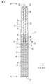
- FIG. 1 is a perspective view of the probe 1 according to the first embodiment of the present invention.
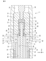
- FIG. 2 is a top view of the probe 1 shown in FIG.
- FIG. 3 is a cross-sectional view taken along the line III-III of probe 1 shown in FIG.
- FIG. 4 is an exploded perspective view of the probe 1 shown in FIG.
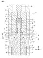
- FIG. 5 is an enlarged cross-sectional view of a main part of the probe 1 shown in FIG.
- the probe 1 includes a barrel 10, a measuring pin 20, a first bushing 30, a second bushing 40, a socket 50, and a coaxial cable 70.
- the probe 1 extends from the proximal end side A (that is, the one end side A) to the distal end side B (that is, the other end side B) in the extending direction of the probe 1 (in the X-axis direction in FIGS. 2 and 3).
- the probe 1 measures the electrical characteristics of the connector (measured object) 2 by elastically contacting the connector terminal (measured terminal) 3 of the connector (measured object) 2, for example.
- the barrel 10 has a barrel body 12 having a cylindrical shape extending in the X-axis direction, and a first accommodating portion 14 formed inside the barrel body 12.
- the tip end side B of the barrel body 12 is opened by the tip through hole 15, and the measurement end portion 22 of the measurement pin 20 is inserted through the tip through hole 15.
- the base end side of the barrel body 12 has a base end opening that is larger than the tip through hole 15, and the coaxial cable 70 is inserted through the base end opening.
- the barrel 10 is a conductive material, such as a metallic material, such as phosphor bronze.
- a first accommodating portion 14 is formed inside the barrel 10.
- the first accommodating portion 14 accommodates a measuring pin 20, a first bushing 30, a second bushing 40, a socket 50, and a coaxial cable 70. Since the barrel 10 covers the outer conductor 76 while having an outer gap 16 with respect to the outer conductor 76 of the coaxial cable 70 described later, it acts as a conductive outer cover member.
- the barrel 10 is formed with an external through hole 18 extending in the thickness direction of the barrel body 12.
- the two external through holes 18 are arranged to face each other at an angle of 180 degrees. The arrangement and number of the external through holes 18 are not limited to this.
- the external through hole 18 has an opening tip portion 19 on the tip end side B of the probe 1.
- the measuring pin 20 is a rod-shaped (needle-shaped) electrode having a built-in spring and can be expanded and contracted, and is also called a contact probe, a spring pin, or a pogo pin.
- the measuring pin 20 has a measuring end 22 on its tip side B and a connecting end 24 on its base end side.
- the measuring pin 20 is a conductive material, for example, a metal material.
- the first bushing 30 is arranged on the tip end side B of the barrel 10.
- the first bushing 30 has a cylindrical shape and is locked to the tip through hole 15 of the barrel 10.
- the first bushing 30 is an electrically insulating material, for example, a resin material.
- the measurement end 22 of the measurement pin 20 is inserted into the first insertion hole of the first bushing 30. Through the first bushing 30, the measuring pin 20 is set in the barrel 10 in an electrically isolated state.
- the second bushing 40 is arranged on the center side of the barrel 10.
- the second bushing 40 is locked by a step portion formed in the central portion of the first accommodating portion 14 of the barrel 10.
- the second bushing 40 has a cylindrical shape.
- the second bushing 40 is an electrically insulating material, for example, a resin material.
- the connection end 24 of the measuring pin 20 is inserted into the small diameter hole of the second insertion hole of the second bushing 40.
- a socket 50 is inserted into the large-diameter hole of the second insertion hole of the second bushing 40.
- the connection end 24 of the measuring pin 20 is in contact with the socket 50.
- the measuring pin 20 is electrically connected to the socket 50 while being supported by the second bushing 40.
- the socket 50 is arranged in the large diameter hole of the second insertion hole of the second bushing 40.
- the socket 50 has a bottomed cylindrical shape.
- the socket 50 is a conductive material, such as a metallic material, such as phosphor bronze. Since the socket 50 covers the central conductor 72 while having a central gap 56 with respect to the central conductor 72 of the coaxial cable 70 described later, it acts as a conductive center cover member.
- a second accommodating portion 54 is formed inside the socket 50.
- the socket 50 has a socket end 57 on the base end side A.
- the socket end 57 serves as a center cover end.
- the socket 50 is formed with a central through hole 58 extending in the thickness direction of the socket 50.
- the two central through holes 58 are arranged to face each other at an angle of 180 degrees. The arrangement and number of the central through holes 58 are not limited to this.
- the coaxial cable 70 has a conductive center conductor 72, a dielectric 74 covering the center conductor 72, an outer conductor 76 covering the dielectric 74, and an electrically insulating outer skin 78 covering the outer conductor 76.
- the tip of the center conductor 72 is exposed from the dielectric 74.
- the dielectric 74 has a dielectric end 75 at the distal end side B of the probe 1.
- the outer conductor 76 has an outer conductor end 77 at the tip end side B of the probe 1.
- the tip of the dielectric 74 including the dielectric end 75 projects from the outer conductor end 77 to the tip side B and is exposed from the outer conductor 76.
- the tip of the outer conductor 76 including the outer conductor end 77 is exposed from the outer skin 78.
- the dielectric end 75 of the dielectric 74 is locked by the base end portion of the second bushing 40.
- the outer conductor end 77 is separated from the tip end side B of the center conductor 72 by the proximal end side A. Thereby, the short circuit prevention effect in the central conductor 72 and the outer conductor 76 can be enhanced.
- the corner portion of the dielectric end 75 of the dielectric 74 is in contact with the edge portion of the second bushing 40 which is the end portion of the proximal end side A and has a tapered shape defining the socket insertion portion 44.
- the loading area of the solder 61 and the loading area of the solder 64 can be partitioned, so that it is possible to prevent the solder 61 and the solder 64 from coming into contact with each other and short-circuiting.
- an external gap 16 is formed between the outer peripheral surface of the conductor of the outer conductor 76 and the inner peripheral surface 13 of the barrel of the barrel body 12.
- the tip of the center conductor 72 is inserted into and accommodated in the second accommodating portion 54 of the socket 50.
- a central gap 56 is formed between the outer peripheral surface of the central conductor 72 of the central conductor 72 and the inner peripheral surface of the socket of the socket 50.
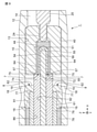
- a central conductor connecting structure (conductor connecting structure) 7 is provided for the central conductor 72 of the coaxial cable 70, and an external conductor connecting structure (conductor connecting structure) 8 is provided for the outer conductor 76. Is provided.
- the socket 50 that acts as a center cover member is configured to cover the center conductor 72 while having a center gap 56 with respect to the center conductor 72 in order to insert the tip end portion of the center conductor 72 into the socket insertion portion 44. ..
- Solder 64 is arranged to fix and electrically connect the tip of the center conductor 72 to the socket 50. This facilitates fixing and electrical connection of the tip of the center conductor 72 to the socket 50.
- the solder 64 acts as a central connecting portion and also as a central connecting member. The solder 64 is supplied from the central through hole 58 to fill the central gap 56. This makes it easy to supply the solder 64 to the central gap 56.
- the central through hole 58 serves as a solder supply unit.
- the central through hole 58 is, for example, a round through hole when viewed from the Z-axis direction.
- the central through hole 58 is arranged on the base end side A, that is, on the side of the socket end 57.
- the solder 64 supplied from the central through hole 58 fills at least the proximal end side A of the central gap 56.
- the solder 64 disposed in the central gap 56 has a central connection end 65 on the base end side A.
- the center connection end 65 of the solder 64 is located from the socket end 57 of the socket 50 to the proximal end side A, and is located between the socket end 57 and the dielectric end 75.
- the center connection end 65 is flush with, for example, the socket end 57.
- the center connection end 65 of the solder 64 is configured to be flush with the socket end 57 of the socket 50.
- the current path from the center conductor 72 to the socket 50 is the center conductor outer peripheral surface 82 of the center conductor 72, the center connection end 65 of the solder 64, the socket end 57 of the socket 50, and the socket. It becomes the socket outer peripheral surface 51 of 50. Therefore, in the above-mentioned central conductor connection structure 7, since the current path does not have a return path, unnecessary resonance is suppressed, and the electrical characteristics of the object 2 to be measured can be measured accurately.
- the barrel 10 that acts as an outer cover member is configured to cover the outer conductor 76 while having an outer gap 16 with respect to the outer conductor 76 in order to insert the coaxial cable 70 into the first accommodating portion 14.
- Solder 61 is arranged to fix and electrically connect the barrel 10 to the outer conductor 76. This facilitates the fixation and electrical connection of the outer conductor 76 to the barrel 10.
- the solder 61 works as an external connecting portion and also as an external connecting member.
- the solder 61 is supplied from the external through hole 18 to fill the external gap 16. This makes it easy to supply the solder 61 to the external gap 16. Therefore, the external through hole 18 functions as a solder supply unit.
- the external through hole 18 is, for example, a round through hole when viewed from the Z-axis direction.
- the external through hole 18 is arranged on the tip end side B in the barrel main body 12.
- the solder 61 supplied from the external through hole 18 fills at least the tip side B of the external gap 16.
- the solder 61 disposed in the external gap 16 has an external connection end 62 on the tip end side B.
- the outer connection end 62 of the solder 61 is located on the tip end side B from the outer conductor end 77 of the outer conductor 76, and is located between the outer conductor end 77 and the dielectric end 75. ..
- the external connection end 62 is displaced toward the tip end side B with respect to the external conductor end 77, for example.
- the outer conductor end 77 is located on the base end side A of the outer through hole 18 with respect to the opening tip portion 19 formed on the tip side B, and is at a position facing the outer through hole 18. As a result, the outer conductor end 77 is covered with the solder 61, and the external connection end 62 is displaced toward the tip side B from the outer conductor end 77, so that the formation of a return path can be prevented.
- the outer connection end 62 of the solder 61 is configured to be located on the tip side B with respect to the outer conductor end 77 of the outer conductor 76.
- the current path from the outer conductor 76 to the barrel 10 is the outer conductor inner peripheral surface 86 of the outer conductor 76, the outer connection end 62 of the solder 61, and the barrel inner peripheral surface of the barrel 10. It becomes 13. Therefore, in the above-mentioned external conductor connection structure 8, since the current path does not have a return path, unnecessary resonance is suppressed, and the electrical characteristics of the object 2 to be measured can be measured accurately.
- the probe 1 shown in FIG. 6 has the same central conductor connection structure 7 as in the first embodiment, and the external connection end 62 of the solder 61 supplied from the external through hole 18 is connected to the external conductor end 77 of the external conductor 76. On the other hand, it has a central conductor connection structure 7 that is flush with each other.
- an external through hole 18 is arranged on the tip side B.
- the outer through hole 18 is arranged so that the opening tip portion 19 on the tip end side B is aligned with the outer conductor end 77 of the outer conductor 76.
- the solder 61 supplied from the external through hole 18 fills at least the tip side B of the external gap 16.
- the solder 61 disposed in the external gap 16 has an external connection end 62 on the tip end side B.
- the external connection end 62 of the solder 61 is located from the outer conductor end 77 of the outer conductor 76 to the tip end side B, and is located between the outer conductor end 77 and the dielectric end 75. ..
- the external connection end 62 is, for example, flush with respect to the external conductor end 77.
- the current path from the outer conductor 76 to the barrel 10 is the outer conductor inner peripheral surface 86 of the outer conductor 76, the outer conductor end 77 of the outer conductor 76, and the outer connection end 62 of the solder 61. , And the barrel inner peripheral surface 13 of the barrel 10. Therefore, in the above-mentioned external conductor connection structure 8, since the current path does not have a return path, unnecessary resonance is suppressed, and the electrical characteristics of the object 2 to be measured can be measured accurately.
- the probe 1 shown in FIG. 7 has an outer conductor connection structure 8 similar to that of the first embodiment, and the center connection end 65 of the solder 64 supplied from the center notch 59 is closer to the base end side A than the socket end 57. It has a misaligned center conductor connection structure 7.
- the center notch 59 is arranged so as to be aligned with the socket end 57.
- Solder 64 is arranged to fix and electrically connect the tip of the center conductor 72 to the socket 50.
- the solder 64 acts as a central connecting portion and also as a central connecting member.
- the central notch 59 has a shape such as a semicircle or an ellipse when viewed from the Z-axis direction, and extends in the thickness direction of the socket 50.
- the central notch 59 serves as a solder supply unit.
- the solder 64 supplied from the central notch 59 fills at least the proximal end side A of the central gap 56. This facilitates fixing and electrical connection of the tip of the center conductor 72 to the socket 50.
- the solder 64 disposed in the central gap 56 has a central connection end 65 on the base end side A.
- the center connection end 65 of the solder 64 is located from the socket end 57 of the socket 50 to the proximal end side A, and is located between the socket end 57 and the dielectric end 75.
- the center connection end 65 is displaced from the socket end 57 to the base end side A, for example.
- the current path from the center conductor 72 to the socket 50 is the center conductor outer peripheral surface 82 of the center conductor 72, the center connection end 65 of the solder 64, the socket end 57 of the socket 50, and It becomes the socket outer peripheral surface 51 of the socket 50. Therefore, in the above-mentioned central conductor connection structure 7, since the current path does not have a return path, unnecessary resonance is suppressed, and the electrical characteristics of the object 2 to be measured can be measured accurately.
- the probe 1 shown in FIG. 8 has an outer conductor connection structure 8 similar to that of the second embodiment, and the center connection end 65 of the solder 64 supplied from the center notch 59 is flush with the socket end 57. It has a central conductor connection structure 7.
- the central notch 59 is arranged so as to be aligned with the socket end 57.
- the central notch 59 has a shape such as a semicircle or an ellipse when viewed from the Z-axis direction, and extends in the thickness direction of the socket 50.
- the solder 64 supplied from the central notch 59 fills at least the proximal end side A of the central gap 56.
- the solder 64 disposed in the central gap 56 has a central connection end 65 on the base end side A.
- the central connection end 65 of the solder 64 is located from the socket end 57 of the socket 50 to the proximal end side A, and is located between the socket end 57 and the dielectric end 75.
- the center connection end 65 is flush with, for example, the socket end 57.
- the current path from the center conductor 72 to the socket 50 is the center conductor outer peripheral surface 82 of the center conductor 72, the center connection end 65 of the solder 64, the socket end 57 of the socket 50, and It becomes the socket outer peripheral surface 51 of the socket 50. Therefore, in the above-mentioned central conductor connection structure 7, since the current path does not have a return path, unnecessary resonance is suppressed, and the electrical characteristics of the object 2 to be measured can be measured accurately.
- the probe 1 shown in FIG. 9 has an outer conductor connection structure 8 similar to that of the first embodiment, and also has a center conductor connection structure 7 in which the solder 64 fills the center gap 56.
- the socket 50 is arranged so as to fill the central gap 56 without having the central through hole 58 or the central notch 59.
- the solder 64 disposed in the central gap 56 has a central connection end 65 on the base end side A.
- the center connection end 65 of the solder 64 is located from the socket end 57 of the socket 50 to the proximal end side A, and is located between the socket end 57 and the dielectric end 75.
- the center connection end 65 is flush with, for example, the socket end 57.
- the center connection end 65 of the solder 64 may be displaced from the socket end 57 of the socket 50 to the base end side A.
- the current path from the center conductor 72 to the socket 50 is the center conductor outer peripheral surface 82 of the center conductor 72, the center connection end 65 of the solder 64, the socket end 57 of the socket 50, and It becomes the socket outer peripheral surface 51 of the socket 50. Therefore, in the above-mentioned central conductor connection structure 7, since the current path does not have a return path, unnecessary resonance is suppressed, and the electrical characteristics of the object 2 to be measured can be measured accurately.
- the probe 1 shown in FIG. 10 has an outer conductor connection structure 8 similar to that of the second embodiment, and also has a center conductor connection structure 7 in which the solder 64 fills the center gap 56.
- the socket 50 is arranged so as to fill the central gap 56 without having the central through hole 58 or the central notch 59.
- the solder 64 disposed in the central gap 56 has a central connection end 65 on the base end side A.
- the center connection end 65 of the solder 64 is located from the socket end 57 of the socket 50 to the proximal end side A, and is located between the socket end 57 and the dielectric end 75.
- the center connection end 65 is displaced from the socket end 57 to the base end side A, for example.
- the center connection end 65 of the solder 64 may be flush with the socket end 57 of the socket 50.
- the probe 1 shown in FIG. 11 has the same central conductor connection structure 7 as in the first embodiment, and the outer conductor 76 of the coaxial cable 70 is fixed to the barrel 10 by the conductive fitting member 67 and is electrically operated. It has an outer conductor connection structure 8 to be connected.
- a conductive fitting member 67 that works as an external connection portion and also works as an external connection member is fitted in the external gap 16.
- the outer gap 16 is formed between the outer conductor inner peripheral surface 86 of the outer conductor 76 and the barrel inner peripheral surface 13 of the barrel body 12.
- the conductive fitting member 67 is arranged so as to abut on the outer conductor end 77 of the outer conductor 76 and the barrel inner peripheral surface 13 of the barrel 10, respectively. This facilitates the fixation and electrical connection of the outer conductor 76 to the barrel 10.
- the fitting member 67 is a conductive material, for example, a metallic material, for example, phosphor bronze.
- the fitting member 67 has, for example, an annular shape, and has a contact end surface 68, a contact peripheral surface 69, a fitting inner peripheral surface 87, and an external connection end 88.
- the contact end surface 68 is formed on the proximal end side A
- the external connection end 88 is formed on the distal end side B.
- the fitting member 67 is fitted between the outer conductor 76 of the coaxial cable 70 and the second bushing 40, and is press-fitted into the first accommodating portion 14. As a result, the contact end surface 68 abuts on the outer conductor end 77, and the contact peripheral surface 69 abuts on the barrel inner peripheral surface 13.
- the outer conductor 76 of the coaxial cable 70 is fixed and electrically connected to the barrel 10 by the conductive fitting member 67.
- the external connection end 88 of the fitting member 67 is located on the tip end side B from the outer conductor end 77 of the outer conductor 76, and is located between the outer conductor end 77 and the dielectric end 75.
- the external connection end 88 is displaced toward the tip end side B with respect to the outer conductor end 77, for example.
- the current path from the outer conductor 76 to the barrel 10 is the outer conductor inner peripheral surface 86 of the outer conductor 76, the fitting inner peripheral surface 87 of the fitting member 67, the outer connecting end 88, and the outer connecting end 88. , It becomes the barrel inner peripheral surface 13 of the barrel 10. Therefore, in the above-mentioned external conductor connection structure 8, since the current path does not have a return path, unnecessary resonance is suppressed, and the electrical characteristics of the object 2 to be measured can be measured accurately.
- the contact end surface 68 is located on the proximal end side A of the external through hole 18 with respect to the opening tip portion 19 formed on the distal end side B, and is at a position facing the external through hole 18.
- the position of the fitting member 67 can be visually recognized through the external through hole 18.
- the solder 61 can be supplied from the external through hole 18 to electrically connect the external conductor 76 and the fitting member 67. This can reinforce the electrical connection.
- the fitting member 67 may be configured to be integrated with the barrel 10.
- the central through hole 58 is arranged on the proximal end side A.
- the solder 64 supplied from the central through hole 58 fills at least the proximal end side A of the central gap 56.
- the solder 64 disposed in the central gap 56 has a central connection end 65 on the base end side A.
- the center connection end 65 of the solder 64 is located from the socket end 57 of the socket 50 to the proximal end side A, and is located between the socket end 57 and the dielectric end 75.
- the center connection end 65 is flush with, for example, the socket end 57.
- the current path from the center conductor 72 to the socket 50 is the center conductor outer peripheral surface 82 of the center conductor 72, the center connection end 65 of the solder 64, the socket end 57 of the socket 50, and It becomes the socket outer peripheral surface 51 of the socket 50. Therefore, in the above-mentioned central conductor connection structure 7, since the current path does not have a return path, unnecessary resonance is suppressed, and the electrical characteristics of the object 2 to be measured can be measured accurately.
- the probe 1 shown in FIG. 12 has an outer conductor connection structure 8 similar to that of the seventh embodiment, and the solder 64 supplied from the center notch 59 fills the base end side A of the center gap 56 with the center conductor connection structure 7. Has.
- the center notch 59 is arranged so as to be aligned with the socket end 57.
- the central notch 59 has a shape such as a semicircle or an ellipse when viewed from the Z-axis direction, and extends in the thickness direction of the socket 50.
- the socket end 57 is in contact with the dielectric end 75.
- the solder 64 supplied from the central notch 59 fills at least the proximal end side A of the central gap 56.
- the solder 64 disposed in the central gap 56 has a central connection end 65 on the base end side A.
- the central connection end 65 of the solder 64 is located from the socket end 57 of the socket 50 to the proximal end side A, and is located between the socket end 57 and the dielectric end 75.
- the center connection end 65 is flush with, for example, the socket end 57.
- the current path from the center conductor 72 to the socket 50 is the center conductor outer peripheral surface 82 of the center conductor 72, the center connection end 65 of the solder 64, the socket end 57 of the socket 50, and It becomes the socket outer peripheral surface 51 of the socket 50. Therefore, in the above-mentioned central conductor connection structure 7, since the current path does not have a return path, unnecessary resonance is suppressed, and the electrical characteristics of the object 2 to be measured can be measured accurately.
- the probe 1 shown in FIG. 13 has an outer conductor connection structure 8 similar to that of the seventh embodiment, and also has a center conductor connection structure 7 in which the solder 64 fills the center gap 56.
- the socket 50 is arranged so as to fill the central gap 56 without the central through hole 58 or the central notch 59.
- the socket end 57 is in contact with the dielectric end 75.
- the solder 64 disposed in the central gap 56 has a central connection end 65 on the base end side A.
- the center connection end 65 of the solder 64 is located from the socket end 57 of the socket 50 to the proximal end side A, and is located between the socket end 57 and the dielectric end 75.
- the center connection end 65 is flush with, for example, the socket end 57.
- the current path from the center conductor 72 to the socket 50 is the center conductor outer peripheral surface 82 of the center conductor 72, the center connection end 65 of the solder 64, the socket end 57 of the socket 50, and It becomes the socket outer peripheral surface 51 of the socket 50. Therefore, in the above-mentioned central conductor connection structure 7, since the current path does not have a return path, unnecessary resonance is suppressed, and the electrical characteristics of the object 2 to be measured can be measured accurately.
- the probe 1 includes both the central conductor connection structure 7 and the outer conductor connection structure 8, but can include at least one of the center conductor connection structure 7 and the outer conductor connection structure 8.
- the above embodiment is an example, and the central conductor connection structure 7 and the outer conductor connection structure 8 in the above embodiment can be appropriately combined.
- the external connection portions 61 and 67 are separate members from the external cover member 10. As a result, the external connection ends 62 and 88 can be positioned with high accuracy. However, the external connection portion can be a part of the external cover member 10.
- the outer cover member 10 has, as an external connecting portion,, for example, an external protruding portion that projects toward the external conductor 76 and presses against the external conductor 76 at a location corresponding to the external through hole 18. Such an external protrusion is formed by caulking. As a result, the external protrusion is joined to the external conductor 76 and is electrically connected to the external conductor 76.
- the external protrusion has, for example, a circular or rectangular shape when viewed from the Z-axis direction, and has a rectangular cross section.
- the external protrusion has an external connection end on the other end side (tip side) B.
- the external connection end of the external protrusion is located on the other end side (tip side) B from the external conductor end 77.
- the external connection end of the external protrusion is displaced toward the other end side (tip side) B from the external conductor end 77, or is a surface with respect to the external conductor end 77, similarly to the external connection ends 62 and 88 described above. It is one.
- the central connection portion 64 is a member separate from the central cover member 50.
- the center connection end 65 can be positioned with high accuracy.
- the central connection portion 64 can be a part of the central cover member 50.
- the central cover member 50 has, for example, a central protruding portion that projects toward the central conductor 72 and presses against the central conductor 72 at a position corresponding to the central through hole 58 or the central notch 59.
- Such a central protrusion is formed by caulking.
- the central protrusion is joined to the central conductor 72 and is electrically connected to the central conductor 72.
- the central protrusion has, for example, a circular or rectangular shape when viewed from the Z-axis direction, and has a rectangular cross section.
- the central protrusion has a central connection end on the proximal end side A.
- the central connection end of the central protrusion is located on the base end side A from the central cover end 57.
- the central connection end of the central protrusion is displaced toward the proximal end side A from the central cover end 57 or is flush with the central cover end 57, similarly to the central connection end 65 described above.
- the shapes of the central through hole 58, the central notch 59, and the external through hole 18 that act as solder feeders are exemplary and, when viewed from the Z-axis direction, are, for example, square, rectangular, trapezoidal, parallelogram, oval, egg. It can have various shapes such as shape, semi-oval, and semi-oval.
- the solder 64 may be present in the central through hole 58 and the central notch 59, and the solder 61 may be present in the external through hole 18.
- the tip of the central conductor 72 protrudes from the dielectric 74
- the tip of the dielectric 74 protrudes from the outer conductor 76
- the tip of the outer conductor 76 protrudes from the outer skin 78. ing.
- the short circuit prevention effect in the central conductor 72 and the outer conductor 76 can be enhanced.
- the conductor connection structure 8 is Base end side A having a measuring pin 20 to which a coaxial cable 70 in which a central conductor 72, a dielectric 74 and an outer conductor 76 are coaxially arranged is connected, and which is electrically connected to the central conductor 72 of the coaxial cable 70.
- the conductor connection structure 8 in the probe 1 extending from the tip side B to the tip side B.
- a conductive outer cover member 10 that covers the outer conductor 76 while having a gap 16.
- a conductive external connecting portion 61, 67 for fixing and electrically connecting the external conductor 76 to the external cover member 10 is provided.
- the external connection ends 62, 88 which are the ends of the tip side B of the probe 1 in the external connection portions 61, 67, are relative to the outer conductor end 77, which is the end of the tip side B of the probe 1 in the outer conductor 76. , It is located flush with each other, or is located on the distal end side B of the probe 1.
- the external connection ends 62, 88 are located on the other end side (tip side) B from the outer conductor end 77, which means that the external connection ends 62, 88 are on the other end side (tip side) of the outer conductor end 77. ) It means that it is located offset from B or is flush with respect to the outer conductor end 77.
- the external connection ends 62, 88 are located between the dielectric end 75, which is the end of the tip end side B of the probe 1 in the dielectric 74, and the external conductor end 77.
- the short circuit prevention effect of the central conductor 72 and the outer conductor 76 can be enhanced.
- the outer cover member 10 has an outer through hole 18 extending in the thickness direction thereof.
- the outer conductor end 77 is located on the proximal end side A of the probe 1 with respect to the opening tip 19 formed on the distal end side B of the probe 1 in the external through hole 18, and faces the outer through hole 18. Is in a position to do.
- the position of the external conductor end 77 can be confirmed through the external through hole 18, and it can be confirmed whether or not the external conductor 76 and the external connecting portions 61 and 67 are electrically connected.
- the external connection portion is solder 61, and is The external through hole 18 serves as a solder supply unit for supplying the solder 61.
- the external connection portion 61 is a fitting member 67 that is fitted into the gap 16.
- the outer conductor end 77 is separated from the distal end side B of the probe 1 in the central conductor 72 to the proximal end side A of the probe 1.
- the short circuit prevention effect of the central conductor 72 and the outer conductor 76 can be enhanced.
- the object 2 to be measured measured by the probe 1 is the connector 2.
- the electrical characteristics of the connector 2 can be measured with high accuracy.
- the probe 1 according to another aspect of the present invention is It is characterized by including the conductor connection structure 8 described above.
- the conductor connection structure 7 is Base end side A having a measuring pin 20 to which a coaxial cable 70 in which a central conductor 72, a dielectric 74 and an outer conductor 76 are coaxially arranged is connected, and which is electrically connected to the central conductor 72 of the coaxial cable 70.
- the conductor connection structure 7 in the probe 1 extending from the tip side B to the tip side B.
- a conductive center cover member 50 that covers the center conductor 72 while having a gap 56,
- a conductive center connecting portion 64 for fixing and electrically connecting the center conductor 72 to the center cover member 50 is provided.
- the central connection end 65 which is the end of the proximal end side A of the probe 1 in the central connection portion 64, is relative to the central cover end 57, which is the end of the proximal end side A of the probe 1 in the central cover member 50. It is located flush with each other or on the proximal end side A of the probe 1.
- the center connection end 65 is located on the base end side A from the center cover end 57 means that the center connection end 65 is displaced from the center cover end 57 to the base end side A, or the center cover end. It means that it is flush with 57.
- the center connection end 65 is located between the dielectric end 75, which is the end of the tip end side B of the probe 1 in the dielectric 74, and the center cover end 57.
- the short circuit prevention effect of the central conductor 72 and the outer conductor 76 can be enhanced.
- the central cover member has a central through hole 58 or a central notch 59 extending in the thickness direction of the central cover member 50.
- the central connection portion 64 is supplied through the central through hole 58 or the central notch 59.
- the central connection portion 64 is a solder 64.
- the outer conductor end 77 which is the end of the distal end side B of the probe 1 in the outer conductor 76, is separated from the distal end side B of the probe 1 in the central conductor 72 with respect to the proximal end side A of the probe 1. There is.
- the short circuit prevention effect of the central conductor 72 and the outer conductor 76 can be enhanced.
- the object 2 to be measured measured by the probe 1 is the connector 2.
- the electrical characteristics of the connector 2 can be measured with high accuracy.
- the probe 1 according to another aspect of the present invention is It is characterized by including the conductor connection structure 7 described above.
- Probe 2 Connector (measured object) 3: Connector terminal (measured terminal) 7: Center conductor connection structure (conductor connection structure) 8: External conductor connection structure (conductor connection structure) 10: Barrel (external cover member) 12: Barrel body 13: Barrel inner peripheral surface 14: First accommodating part 15: Tip through hole 16: External gap (gap) 18: External through hole (solder supply part) 19: Opening tip 20: Measuring pin 22: Measuring end 24: Connection end 30: First bushing 40: Second bushing 44: Socket insertion part 50: Socket (center cover member) 51: Socket outer peripheral surface 54: Second accommodating part 56: Center gap (gap) 57: Socket end (center cover end) 58: Central through hole (solder supply part) 59: Central notch (solder supply section) 61: Solder (external connection part, external connection member) 62: External connection end 64: Solder (center connection part, center connection member) 65: Center connection end end
Abstract
Provided is a conductor connecting structure for accurately measuring an electrical property of an object being measured. A conductor connecting structure 8 of a probe 1 which extends from a base end side A to a tip end side B, to which a coaxial cable 70 comprising a central conductor 72, a dielectric 74 and an outer conductor 76 that are arranged coaxially is connected, and which has a measuring pin 20 that is electrically connected to the central conductor of the coaxial cable, is provided with an electrically conductive outer cover member 10 which covers the outer conductor across a gap 16, and an electrically conductive outer connecting portion 61, 67 which fixes and electrically connects the outer conductor to the outer cover member, wherein an outer connecting end 62, 88, which is the end of the outer connecting portion on the probe tip end side, is positioned flush with an outer conductor end 77, which is the end of the outer conductor on the probe tip end side, or is positioned on the probe tip end side of the outer conductor end 77.
Description
この発明は、導体接続構造および該導体接続構造を備えるプローブに関する。
The present invention relates to a conductor connection structure and a probe provided with the conductor connection structure.
例えば、特許文献1は、同軸ケーブルの先端に接続される検査用同軸コネクタを開示する。特許文献1の検査用同軸コネクタでは、同軸ケーブルの中心導体および外部導体が、それぞれ、同軸コネクタ用のソケットに電気的に接続されるとともに、同軸コネクタ用のソケットを介して検査用同軸コネクタに接続されている。
For example, Patent Document 1 discloses an inspection coaxial connector connected to the tip of a coaxial cable. In the inspection coaxial connector of Patent Document 1, the central conductor and the outer conductor of the coaxial cable are electrically connected to the socket for the coaxial connector and connected to the inspection coaxial connector via the socket for the coaxial connector, respectively. Has been done.
特許文献1では、同軸ケーブルが同軸コネクタ用のソケットに電気的に接続されると記載されているものの、電気的接続がどのような構造であるかについて具体的に開示されていない。
Although Patent Document 1 describes that a coaxial cable is electrically connected to a socket for a coaxial connector, it does not specifically disclose what kind of structure the electrical connection has.
ところで、導体を流れる信号が、マイクロ波やミリ波のような高周波の帯域になると、表皮効果により電流密度が導体表面に集中する。導体と、導体に対して隙間を有しながら導体を覆う導電性のカバー部材とを導電性の接続部材で接続する場合、接続部材の位置が適切ではないと、電流経路が戻り経路を有することによって電流経路が複雑になる。電流経路が複雑になると不要な共振が発生することによって、被測定物の電気特性を精度良く測定することが妨げられる。
By the way, when the signal flowing through the conductor is in the high frequency band such as microwaves and millimeter waves, the current density is concentrated on the conductor surface due to the skin effect. When connecting a conductor and a conductive cover member that covers the conductor with a gap with respect to the conductor with a conductive connecting member, if the position of the connecting member is not appropriate, the current path has a return path. Complicates the current path. When the current path becomes complicated, unnecessary resonance occurs, which hinders accurate measurement of the electrical characteristics of the object to be measured.
したがって、この発明の解決すべき技術的課題は、被測定物の電気特性を精度良く測定する導体接続構造および該導体接続構造を備えるプローブを提供することである。
Therefore, the technical problem to be solved by the present invention is to provide a conductor connection structure for accurately measuring the electrical characteristics of the object to be measured and a probe having the conductor connection structure.
上記技術的課題を解決するために、この発明によれば、以下の導体接続構造が提供される。
In order to solve the above technical problems, according to the present invention, the following conductor connection structure is provided.
すなわち、この発明に係る導体接続構造は、
中心導体、誘電体および外部導体が同軸に配置された同軸ケーブルが接続され、前記同軸ケーブルの前記中心導体に電気的に接続される測定ピンを有する、基端側から先端側に延在するプローブにおける導体接続構造であって、
前記外部導体に対して隙間を有しながら覆う導電性の外部カバー部材と、
前記外部導体を前記外部カバー部材に対して固定し且つ電気的に接続する導電性の外部接続部とを備え、
前記外部接続部における前記プローブの先端側の端である外部接続端は、前記外部導体における前記プローブの先端側の端である外部導体端に対して、面一に位置するか、または、前記プローブの先端側に位置することを特徴とする。 That is, the conductor connection structure according to the present invention is
A probe extending from the proximal end side to the distal end side having a measuring pin to which a coaxial cable in which a central conductor, a dielectric and an outer conductor are arranged coaxially is connected and electrically connected to the central conductor of the coaxial cable. It is a conductor connection structure in
A conductive outer cover member that covers the outer conductor with a gap,
It is provided with a conductive external connection portion for fixing and electrically connecting the external conductor to the external cover member.
The external connection end, which is the distal end of the probe in the external connection, is either flush with the external conductor end, which is the distal end of the probe in the external conductor, or the probe. It is characterized by being located on the tip side of.
この発明によれば、電流経路が戻り経路を有さないことによって、不要な共振が抑制されるので、被測定物の電気特性を精度良く測定できる。
According to the present invention, since the current path does not have a return path, unnecessary resonance is suppressed, so that the electrical characteristics of the object to be measured can be measured with high accuracy.
以下、この発明に係る、導体接続構造7,8および該導体接続構造7,8を備えるプローブ1の実施形態について、図面を参照しながら説明する。
Hereinafter, an embodiment of the probe 1 having the conductor connection structures 7 and 8 and the conductor connection structures 7 and 8 according to the present invention will be described with reference to the drawings.
〔第1実施形態〕
図1~図5を参照しながら、第1実施形態に係るプローブ1を説明する。図1は、この発明の第1実施形態に係るプローブ1の斜視図である。図2は、図1に示したプローブ1の上面図である。図3は、図2に示したプローブ1のIII-III線に沿った断面図である。図4は、図1に示したプローブ1の分解斜視図である。図5は、図3に示したプローブ1の要部拡大断面図である。 [First Embodiment]
Theprobe 1 according to the first embodiment will be described with reference to FIGS. 1 to 5. FIG. 1 is a perspective view of the probe 1 according to the first embodiment of the present invention. FIG. 2 is a top view of the probe 1 shown in FIG. FIG. 3 is a cross-sectional view taken along the line III-III of probe 1 shown in FIG. FIG. 4 is an exploded perspective view of the probe 1 shown in FIG. FIG. 5 is an enlarged cross-sectional view of a main part of the probe 1 shown in FIG.
図1~図5を参照しながら、第1実施形態に係るプローブ1を説明する。図1は、この発明の第1実施形態に係るプローブ1の斜視図である。図2は、図1に示したプローブ1の上面図である。図3は、図2に示したプローブ1のIII-III線に沿った断面図である。図4は、図1に示したプローブ1の分解斜視図である。図5は、図3に示したプローブ1の要部拡大断面図である。 [First Embodiment]
The
図1~図4に示すように、プローブ1は、バレル10と、測定ピン20と、第1ブッシング30と、第2ブッシング40と、ソケット50と、同軸ケーブル70とを備える。プローブ1は、基端側A(すなわち一端側A)から先端側B(すなわち他端側B)に、プローブ1の延在方向(図2および図3ではX軸方向)に延在する。プローブ1は、例えば、コネクタ(被測定物)2のコネクタ端子(被測定端子)3に対して弾性的に当接することによって、コネクタ(被測定物)2の電気特性を測定する。
As shown in FIGS. 1 to 4, the probe 1 includes a barrel 10, a measuring pin 20, a first bushing 30, a second bushing 40, a socket 50, and a coaxial cable 70. The probe 1 extends from the proximal end side A (that is, the one end side A) to the distal end side B (that is, the other end side B) in the extending direction of the probe 1 (in the X-axis direction in FIGS. 2 and 3). The probe 1 measures the electrical characteristics of the connector (measured object) 2 by elastically contacting the connector terminal (measured terminal) 3 of the connector (measured object) 2, for example.
バレル10は、X軸方向に延びる円筒形状を有するバレル本体12と、バレル本体12の内部に形成される第1収容部14とを有する。バレル本体12の先端側Bは、先端貫通孔15によって開口しており、先端貫通孔15には測定ピン20の測定端部22が挿通される。バレル本体12の基端側は、先端貫通孔15よりも大きく開口した基端開口を有しており、基端開口には同軸ケーブル70が挿通される。バレル10は、導電性材料、例えば金属材料であり、例えばリン青銅である。
The barrel 10 has a barrel body 12 having a cylindrical shape extending in the X-axis direction, and a first accommodating portion 14 formed inside the barrel body 12. The tip end side B of the barrel body 12 is opened by the tip through hole 15, and the measurement end portion 22 of the measurement pin 20 is inserted through the tip through hole 15. The base end side of the barrel body 12 has a base end opening that is larger than the tip through hole 15, and the coaxial cable 70 is inserted through the base end opening. The barrel 10 is a conductive material, such as a metallic material, such as phosphor bronze.
バレル10の内部には、第1収容部14が形成される。第1収容部14には、測定ピン20、第1ブッシング30、第2ブッシング40、ソケット50および同軸ケーブル70が収容される。バレル10は、後述する同軸ケーブル70の外部導体76に対して外部隙間16を有しながら外部導体76を覆うので、導電性の外部カバー部材として働く。バレル10には、バレル本体12の厚み方向に延在する外部貫通孔18が形成されている。例えば、2つの外部貫通孔18が、180度の角度で対向配置される。外部貫通孔18の配置や個数は、これに限定されるものではない。外部貫通孔18は、プローブ1の先端側Bにおいて、開口先端部19を有する。
A first accommodating portion 14 is formed inside the barrel 10. The first accommodating portion 14 accommodates a measuring pin 20, a first bushing 30, a second bushing 40, a socket 50, and a coaxial cable 70. Since the barrel 10 covers the outer conductor 76 while having an outer gap 16 with respect to the outer conductor 76 of the coaxial cable 70 described later, it acts as a conductive outer cover member. The barrel 10 is formed with an external through hole 18 extending in the thickness direction of the barrel body 12. For example, the two external through holes 18 are arranged to face each other at an angle of 180 degrees. The arrangement and number of the external through holes 18 are not limited to this. The external through hole 18 has an opening tip portion 19 on the tip end side B of the probe 1.
測定ピン20は、バネが内蔵されていて伸縮可能な棒状(針状)の電極であり、コンタクトプローブ、スプリングピンまたはポゴピンとも呼ばれる。測定ピン20は、その先端側Bに測定端部22を有するとともに、その基端側に接続端部24を有する。測定ピン20は、導電性材料、例えば金属材料である。
The measuring pin 20 is a rod-shaped (needle-shaped) electrode having a built-in spring and can be expanded and contracted, and is also called a contact probe, a spring pin, or a pogo pin. The measuring pin 20 has a measuring end 22 on its tip side B and a connecting end 24 on its base end side. The measuring pin 20 is a conductive material, for example, a metal material.
第1ブッシング30は、バレル10の先端側Bに配設される。第1ブッシング30は、円筒形状を有し、バレル10の先端貫通孔15に係止される。第1ブッシング30は、電気絶縁性材料、例えば樹脂材料である。第1ブッシング30の第1挿入孔には、測定ピン20の測定端部22が挿通される。第1ブッシング30を介することにより、測定ピン20は、電気的に絶縁された状態でバレル10にセットされる。
The first bushing 30 is arranged on the tip end side B of the barrel 10. The first bushing 30 has a cylindrical shape and is locked to the tip through hole 15 of the barrel 10. The first bushing 30 is an electrically insulating material, for example, a resin material. The measurement end 22 of the measurement pin 20 is inserted into the first insertion hole of the first bushing 30. Through the first bushing 30, the measuring pin 20 is set in the barrel 10 in an electrically isolated state.
第2ブッシング40は、バレル10の中央側に配設される。第2ブッシング40は、バレル10の第1収容部14の中央部に形成された段差部によって係止される。第2ブッシング40は、円筒形状を有する。第2ブッシング40は、電気絶縁性材料、例えば樹脂材料である。第2ブッシング40の第2挿入孔の小径孔には、測定ピン20の接続端部24が挿通される。第2ブッシング40の第2挿入孔の大径孔には、ソケット50が挿通される。測定ピン20の接続端部24がソケット50に接触している。測定ピン20は、第2ブッシング40に支持された状態でソケット50に電気的に接続される。
The second bushing 40 is arranged on the center side of the barrel 10. The second bushing 40 is locked by a step portion formed in the central portion of the first accommodating portion 14 of the barrel 10. The second bushing 40 has a cylindrical shape. The second bushing 40 is an electrically insulating material, for example, a resin material. The connection end 24 of the measuring pin 20 is inserted into the small diameter hole of the second insertion hole of the second bushing 40. A socket 50 is inserted into the large-diameter hole of the second insertion hole of the second bushing 40. The connection end 24 of the measuring pin 20 is in contact with the socket 50. The measuring pin 20 is electrically connected to the socket 50 while being supported by the second bushing 40.
ソケット50は、第2ブッシング40の第2挿入孔の大径孔に配設される。ソケット50は、有底円筒形状を有する。ソケット50は、導電性材料、例えば金属材料であり、例えばリン青銅である。ソケット50は、後述する同軸ケーブル70の中心導体72に対して中心隙間56を有しながら中心導体72を覆うので、導電性の中心カバー部材として働く。ソケット50の内部には、第2収容部54が形成されている。ソケット50は、基端側Aに、ソケット端57を有する。ソケット端57は、中心カバー端として働く。ソケット50には、ソケット50の厚み方向に延在する中心貫通孔58が形成されている。例えば、2つの中心貫通孔58が、180度の角度で対向配置される。中心貫通孔58の配置や個数は、これに限定されるものではない。
The socket 50 is arranged in the large diameter hole of the second insertion hole of the second bushing 40. The socket 50 has a bottomed cylindrical shape. The socket 50 is a conductive material, such as a metallic material, such as phosphor bronze. Since the socket 50 covers the central conductor 72 while having a central gap 56 with respect to the central conductor 72 of the coaxial cable 70 described later, it acts as a conductive center cover member. A second accommodating portion 54 is formed inside the socket 50. The socket 50 has a socket end 57 on the base end side A. The socket end 57 serves as a center cover end. The socket 50 is formed with a central through hole 58 extending in the thickness direction of the socket 50. For example, the two central through holes 58 are arranged to face each other at an angle of 180 degrees. The arrangement and number of the central through holes 58 are not limited to this.
同軸ケーブル70は、導電性の中心導体72と、中心導体72を覆う誘電体74と、誘電体74を覆う外部導体76と、外部導体76を覆う電気絶縁性の外皮78とを有する。中心導体72の先端部は、誘電体74から露出している。誘電体74は、プローブ1の先端側Bにおいて、誘電端75を有する。外部導体76は、プローブ1の先端側Bにおいて、外部導体端77を有する。誘電端75を含む誘電体74の先端部は、外部導体端77から先端側Bに突出するとともに外部導体76から露出している。外部導体端77を含む外部導体76の先端部は、外皮78から露出している。外皮78を含む同軸ケーブル70が、バレル10の第1収容部14に挿入されると、誘電体74の誘電端75は、第2ブッシング40の基端部によって係止される。外部導体端77が、中心導体72の先端側Bに対して、基端側Aに離間している。これにより、中心導体72および外部導体76における短絡防止効果を高めることができる。
The coaxial cable 70 has a conductive center conductor 72, a dielectric 74 covering the center conductor 72, an outer conductor 76 covering the dielectric 74, and an electrically insulating outer skin 78 covering the outer conductor 76. The tip of the center conductor 72 is exposed from the dielectric 74. The dielectric 74 has a dielectric end 75 at the distal end side B of the probe 1. The outer conductor 76 has an outer conductor end 77 at the tip end side B of the probe 1. The tip of the dielectric 74 including the dielectric end 75 projects from the outer conductor end 77 to the tip side B and is exposed from the outer conductor 76. The tip of the outer conductor 76 including the outer conductor end 77 is exposed from the outer skin 78. When the coaxial cable 70 including the outer skin 78 is inserted into the first accommodating portion 14 of the barrel 10, the dielectric end 75 of the dielectric 74 is locked by the base end portion of the second bushing 40. The outer conductor end 77 is separated from the tip end side B of the center conductor 72 by the proximal end side A. Thereby, the short circuit prevention effect in the central conductor 72 and the outer conductor 76 can be enhanced.
誘電体74の誘電端75のコーナー部は、第2ブッシング40において基端側Aの端部であってソケット挿入部44を画定するテーパー形状を有する縁部に当接している。これにより、ハンダ61の装填領域とハンダ64の装填領域とを仕切ることができるので、ハンダ61およびハンダ64が接触して短絡することを防止できる。
The corner portion of the dielectric end 75 of the dielectric 74 is in contact with the edge portion of the second bushing 40 which is the end portion of the proximal end side A and has a tapered shape defining the socket insertion portion 44. As a result, the loading area of the solder 61 and the loading area of the solder 64 can be partitioned, so that it is possible to prevent the solder 61 and the solder 64 from coming into contact with each other and short-circuiting.
同軸ケーブル70が、バレル10の第1収容部14に挿入されるとき、外部導体76の導体外周面とバレル本体12のバレル内周面13との間には、外部隙間16が形成される。中心導体72の先端部が、ソケット50の第2収容部54に挿入されて収容される。このとき、中心導体72の中心導体外周面82とソケット50のソケット内周面との間には、中心隙間56が形成される。
When the coaxial cable 70 is inserted into the first accommodating portion 14 of the barrel 10, an external gap 16 is formed between the outer peripheral surface of the conductor of the outer conductor 76 and the inner peripheral surface 13 of the barrel of the barrel body 12. The tip of the center conductor 72 is inserted into and accommodated in the second accommodating portion 54 of the socket 50. At this time, a central gap 56 is formed between the outer peripheral surface of the central conductor 72 of the central conductor 72 and the inner peripheral surface of the socket of the socket 50.
図5を参照しながら、第1実施形態に係るプローブ1の導体接続構造7,8を説明する。
The conductor connection structures 7 and 8 of the probe 1 according to the first embodiment will be described with reference to FIG.
図5に示すように、同軸ケーブル70の中心導体72に対して中心導体接続構造(導体接続構造)7が設けられているとともに、外部導体76に対して外部導体接続構造(導体接続構造)8が設けられている。
As shown in FIG. 5, a central conductor connecting structure (conductor connecting structure) 7 is provided for the central conductor 72 of the coaxial cable 70, and an external conductor connecting structure (conductor connecting structure) 8 is provided for the outer conductor 76. Is provided.
まず、中心導体接続構造(導体接続構造)7を説明する。中心カバー部材として働くソケット50は、中心導体72の先端部をソケット挿入部44に挿入するために、中心導体72に対して中心隙間56を有しながら中心導体72を覆うように構成されている。ソケット50に対して中心導体72の先端部を固定し且つ電気的に接続するために、ハンダ64が配設されている。これにより、ソケット50に対する中心導体72の先端部の固定および電気的な接続が容易である。ハンダ64は、中心接続部として働くとともに中心接続部材として働く。ハンダ64は、中心貫通孔58から供給されて、中心隙間56を埋める。これにより、中心隙間56へのハンダ64の供給が容易である。したがって、中心貫通孔58は、ハンダ供給部として働く。中心貫通孔58は、Z軸方向から見て、例えば丸い貫通孔である。中心貫通孔58が基端側Aに、すなわち、ソケット端57の側に配設されている。
First, the central conductor connection structure (conductor connection structure) 7 will be described. The socket 50 that acts as a center cover member is configured to cover the center conductor 72 while having a center gap 56 with respect to the center conductor 72 in order to insert the tip end portion of the center conductor 72 into the socket insertion portion 44. .. Solder 64 is arranged to fix and electrically connect the tip of the center conductor 72 to the socket 50. This facilitates fixing and electrical connection of the tip of the center conductor 72 to the socket 50. The solder 64 acts as a central connecting portion and also as a central connecting member. The solder 64 is supplied from the central through hole 58 to fill the central gap 56. This makes it easy to supply the solder 64 to the central gap 56. Therefore, the central through hole 58 serves as a solder supply unit. The central through hole 58 is, for example, a round through hole when viewed from the Z-axis direction. The central through hole 58 is arranged on the base end side A, that is, on the side of the socket end 57.
中心貫通孔58から供給されるハンダ64は、中心隙間56のうち、少なくとも、基端側Aを埋める。中心隙間56に配設されるハンダ64は、基端側Aに、中心接続端65を有する。図5に示す中心導体接続構造7では、ハンダ64の中心接続端65は、ソケット50のソケット端57から基端側Aに位置し、ソケット端57と誘電端75との間に位置する。中心接続端65は、例えば、ソケット端57に対して面一である。
The solder 64 supplied from the central through hole 58 fills at least the proximal end side A of the central gap 56. The solder 64 disposed in the central gap 56 has a central connection end 65 on the base end side A. In the center conductor connection structure 7 shown in FIG. 5, the center connection end 65 of the solder 64 is located from the socket end 57 of the socket 50 to the proximal end side A, and is located between the socket end 57 and the dielectric end 75. The center connection end 65 is flush with, for example, the socket end 57.
中心導体72を流れる信号が、マイクロ波やミリ波のような高周波の帯域になると、表皮効果により電流密度が中心導体72の表面に集中する。図5に示す中心導体接続構造7では、ハンダ64の中心接続端65がソケット50のソケット端57に対して面一であるように構成されている。当該中心導体接続構造7によれば、中心導体72からソケット50への電流経路が、中心導体72の中心導体外周面82、ハンダ64の中心接続端65、ソケット50のソケット端57、および、ソケット50のソケット外周面51になる。したがって、上記の中心導体接続構造7では、電流経路が戻り経路を有さないので、不要な共振が抑制されて、被測定物2の電気特性を精度良く測定できる。
When the signal flowing through the central conductor 72 is in a high frequency band such as microwaves and millimeter waves, the current density is concentrated on the surface of the central conductor 72 due to the skin effect. In the center conductor connection structure 7 shown in FIG. 5, the center connection end 65 of the solder 64 is configured to be flush with the socket end 57 of the socket 50. According to the center conductor connection structure 7, the current path from the center conductor 72 to the socket 50 is the center conductor outer peripheral surface 82 of the center conductor 72, the center connection end 65 of the solder 64, the socket end 57 of the socket 50, and the socket. It becomes the socket outer peripheral surface 51 of 50. Therefore, in the above-mentioned central conductor connection structure 7, since the current path does not have a return path, unnecessary resonance is suppressed, and the electrical characteristics of the object 2 to be measured can be measured accurately.
次に、外部導体接続構造(導体接続構造)8を説明する。外部カバー部材として働くバレル10は、同軸ケーブル70を第1収容部14に挿入するために、外部導体76に対して外部隙間16を有しながら外部導体76を覆うように構成されている。外部導体76に対してバレル10を固定し且つ電気的に接続するために、ハンダ61が配設されている。これにより、バレル10に対する外部導体76の固定および電気的な接続が容易である。ハンダ61は、外部接続部として働くとともに外部接続部材として働く。ハンダ61は、外部貫通孔18から供給されて、外部隙間16を埋める。これにより、外部隙間16へのハンダ61の供給が容易である。したがって、外部貫通孔18は、ハンダ供給部として働く。外部貫通孔18は、Z軸方向から見て、例えば丸い貫通孔である。外部貫通孔18が、バレル本体12において、先端側Bに配設されている。
Next, the outer conductor connection structure (conductor connection structure) 8 will be described. The barrel 10 that acts as an outer cover member is configured to cover the outer conductor 76 while having an outer gap 16 with respect to the outer conductor 76 in order to insert the coaxial cable 70 into the first accommodating portion 14. Solder 61 is arranged to fix and electrically connect the barrel 10 to the outer conductor 76. This facilitates the fixation and electrical connection of the outer conductor 76 to the barrel 10. The solder 61 works as an external connecting portion and also as an external connecting member. The solder 61 is supplied from the external through hole 18 to fill the external gap 16. This makes it easy to supply the solder 61 to the external gap 16. Therefore, the external through hole 18 functions as a solder supply unit. The external through hole 18 is, for example, a round through hole when viewed from the Z-axis direction. The external through hole 18 is arranged on the tip end side B in the barrel main body 12.
外部貫通孔18が、外部導体端77の上に配設されているので、外部貫通孔18から供給されるハンダ61は、外部隙間16のうち、少なくとも、先端側Bを埋める。外部隙間16に配設されるハンダ61は、先端側Bに、外部接続端62を有する。図5に示す外部導体接続構造8では、ハンダ61の外部接続端62は、外部導体76の外部導体端77から先端側Bに位置し、外部導体端77と誘電端75との間に位置する。外部接続端62は、例えば、外部導体端77よりも先端側Bにずれている。外部導体端77が、外部貫通孔18において先端側Bに形成される開口先端部19よりも基端側Aに位置するとともに、外部貫通孔18に対面する位置にある。これにより、外部導体端77がハンダ61で覆われて、外部接続端62が、外部導体端77よりも先端側Bにずれるので、戻り経路の形成を防止できる。
Since the external through hole 18 is arranged on the outer conductor end 77, the solder 61 supplied from the external through hole 18 fills at least the tip side B of the external gap 16. The solder 61 disposed in the external gap 16 has an external connection end 62 on the tip end side B. In the outer conductor connection structure 8 shown in FIG. 5, the outer connection end 62 of the solder 61 is located on the tip end side B from the outer conductor end 77 of the outer conductor 76, and is located between the outer conductor end 77 and the dielectric end 75. .. The external connection end 62 is displaced toward the tip end side B with respect to the external conductor end 77, for example. The outer conductor end 77 is located on the base end side A of the outer through hole 18 with respect to the opening tip portion 19 formed on the tip side B, and is at a position facing the outer through hole 18. As a result, the outer conductor end 77 is covered with the solder 61, and the external connection end 62 is displaced toward the tip side B from the outer conductor end 77, so that the formation of a return path can be prevented.
外部導体76を流れる信号が、マイクロ波やミリ波のような高周波の帯域になると、表皮効果により電流密度が外部導体76の表面に集中する。図5に示す外部導体接続構造8では、ハンダ61の外部接続端62が外部導体76の外部導体端77に対して先端側Bに位置するように構成されている。このような外部導体接続構造8によれば、外部導体76からバレル10への電流経路が、外部導体76の外部導体内周面86、ハンダ61の外部接続端62、バレル10のバレル内周面13になる。したがって、上記の外部導体接続構造8では、電流経路が戻り経路を有さないので、不要な共振が抑制されて、被測定物2の電気特性を精度良く測定できる。
When the signal flowing through the outer conductor 76 is in the high frequency band such as microwaves and millimeter waves, the current density is concentrated on the surface of the outer conductor 76 due to the skin effect. In the outer conductor connection structure 8 shown in FIG. 5, the outer connection end 62 of the solder 61 is configured to be located on the tip side B with respect to the outer conductor end 77 of the outer conductor 76. According to such an outer conductor connection structure 8, the current path from the outer conductor 76 to the barrel 10 is the outer conductor inner peripheral surface 86 of the outer conductor 76, the outer connection end 62 of the solder 61, and the barrel inner peripheral surface of the barrel 10. It becomes 13. Therefore, in the above-mentioned external conductor connection structure 8, since the current path does not have a return path, unnecessary resonance is suppressed, and the electrical characteristics of the object 2 to be measured can be measured accurately.
したがって、上記構成によれば、電流経路が戻り経路を有さないことによって、不要な共振が抑制されるので、被測定物2の電気特性を精度良く測定できる。
Therefore, according to the above configuration, since the current path does not have a return path, unnecessary resonance is suppressed, so that the electrical characteristics of the object 2 to be measured can be measured with high accuracy.
〔第2実施形態〕
図6を参照しながら、第2実施形態に係るプローブ1の導体接続構造7,8を説明するが、上記第1実施形態との相違点を中心に説明する。 [Second Embodiment]
The conductor connection structures 7 and 8 of the probe 1 according to the second embodiment will be described with reference to FIG. 6, but the differences from the first embodiment will be mainly described.
図6を参照しながら、第2実施形態に係るプローブ1の導体接続構造7,8を説明するが、上記第1実施形態との相違点を中心に説明する。 [Second Embodiment]
The
図6に示すプローブ1は、第1実施形態と同様の中心導体接続構造7を有するとともに、外部貫通孔18から供給されるハンダ61の外部接続端62が、外部導体76の外部導体端77に対して面一である中心導体接続構造7を有する。
The probe 1 shown in FIG. 6 has the same central conductor connection structure 7 as in the first embodiment, and the external connection end 62 of the solder 61 supplied from the external through hole 18 is connected to the external conductor end 77 of the external conductor 76. On the other hand, it has a central conductor connection structure 7 that is flush with each other.
図6に示すように、外部貫通孔18が、先端側Bに配設されている。詳細には、外部貫通孔18は、その先端側Bの開口先端部19が、外部導体76の外部導体端77に対して並ぶように配設されている。
As shown in FIG. 6, an external through hole 18 is arranged on the tip side B. Specifically, the outer through hole 18 is arranged so that the opening tip portion 19 on the tip end side B is aligned with the outer conductor end 77 of the outer conductor 76.
外部貫通孔18から供給されるハンダ61は、外部隙間16のうち、少なくとも、先端側Bを埋める。外部隙間16に配設されるハンダ61は、先端側Bに、外部接続端62を有する。図6に示す外部導体接続構造8では、ハンダ61の外部接続端62は、外部導体76の外部導体端77から先端側Bに位置し、外部導体端77と誘電端75との間に位置する。外部接続端62は、例えば、外部導体端77に対して面一である。
The solder 61 supplied from the external through hole 18 fills at least the tip side B of the external gap 16. The solder 61 disposed in the external gap 16 has an external connection end 62 on the tip end side B. In the external conductor connection structure 8 shown in FIG. 6, the external connection end 62 of the solder 61 is located from the outer conductor end 77 of the outer conductor 76 to the tip end side B, and is located between the outer conductor end 77 and the dielectric end 75. .. The external connection end 62 is, for example, flush with respect to the external conductor end 77.
上記の外部導体接続構造8によれば、外部導体76からバレル10への電流経路が、外部導体76の外部導体内周面86、外部導体76の外部導体端77、ハンダ61の外部接続端62、および、バレル10のバレル内周面13になる。したがって、上記の外部導体接続構造8では、電流経路が戻り経路を有さないので、不要な共振が抑制されて、被測定物2の電気特性を精度良く測定できる。
According to the above-mentioned outer conductor connection structure 8, the current path from the outer conductor 76 to the barrel 10 is the outer conductor inner peripheral surface 86 of the outer conductor 76, the outer conductor end 77 of the outer conductor 76, and the outer connection end 62 of the solder 61. , And the barrel inner peripheral surface 13 of the barrel 10. Therefore, in the above-mentioned external conductor connection structure 8, since the current path does not have a return path, unnecessary resonance is suppressed, and the electrical characteristics of the object 2 to be measured can be measured accurately.
したがって、上記構成によれば、電流経路が戻り経路を有さないことによって、不要な共振が抑制されるので、被測定物2の電気特性を精度良く測定できる。
Therefore, according to the above configuration, since the current path does not have a return path, unnecessary resonance is suppressed, so that the electrical characteristics of the object 2 to be measured can be measured with high accuracy.
〔第3実施形態〕
図7を参照しながら、第3実施形態に係るプローブ1の導体接続構造7,8を説明するが、上記第1実施形態との相違点を中心に説明する。 [Third Embodiment]
The conductor connection structures 7 and 8 of the probe 1 according to the third embodiment will be described with reference to FIG. 7, but the differences from the first embodiment will be mainly described.
図7を参照しながら、第3実施形態に係るプローブ1の導体接続構造7,8を説明するが、上記第1実施形態との相違点を中心に説明する。 [Third Embodiment]
The
図7に示すプローブ1は、第1実施形態と同様の外部導体接続構造8を有するとともに、中心切り欠き59から供給されるハンダ64の中心接続端65がソケット端57よりも基端側Aにずれている中心導体接続構造7を有する。
The probe 1 shown in FIG. 7 has an outer conductor connection structure 8 similar to that of the first embodiment, and the center connection end 65 of the solder 64 supplied from the center notch 59 is closer to the base end side A than the socket end 57. It has a misaligned center conductor connection structure 7.
図7に示すように、中心切り欠き59がソケット端57と並ぶように配設されている。ソケット50に対して中心導体72の先端部を固定し且つ電気的に接続するために、ハンダ64が配設されている。ハンダ64は、中心接続部として働くとともに中心接続部材として働く。中心切り欠き59は、Z軸方向から見て、例えば半円や楕円などの形状を有し、ソケット50の厚み方向に延在する。中心切り欠き59は、ハンダ供給部として働く。
As shown in FIG. 7, the center notch 59 is arranged so as to be aligned with the socket end 57. Solder 64 is arranged to fix and electrically connect the tip of the center conductor 72 to the socket 50. The solder 64 acts as a central connecting portion and also as a central connecting member. The central notch 59 has a shape such as a semicircle or an ellipse when viewed from the Z-axis direction, and extends in the thickness direction of the socket 50. The central notch 59 serves as a solder supply unit.
中心切り欠き59から供給されるハンダ64は、中心隙間56のうち、少なくとも、基端側Aを埋める。これにより、ソケット50に対する中心導体72の先端部の固定および電気的な接続が容易である。中心隙間56に配設されるハンダ64は、基端側Aに、中心接続端65を有する。図7に示す中心導体接続構造7では、ハンダ64の中心接続端65は、ソケット50のソケット端57から基端側Aに位置し、ソケット端57と誘電端75との間に位置する。中心接続端65は、例えば、ソケット端57よりも基端側Aにずれている。
The solder 64 supplied from the central notch 59 fills at least the proximal end side A of the central gap 56. This facilitates fixing and electrical connection of the tip of the center conductor 72 to the socket 50. The solder 64 disposed in the central gap 56 has a central connection end 65 on the base end side A. In the center conductor connection structure 7 shown in FIG. 7, the center connection end 65 of the solder 64 is located from the socket end 57 of the socket 50 to the proximal end side A, and is located between the socket end 57 and the dielectric end 75. The center connection end 65 is displaced from the socket end 57 to the base end side A, for example.
上記の中心導体接続構造7によれば、中心導体72からソケット50への電流経路が、中心導体72の中心導体外周面82、ハンダ64の中心接続端65、ソケット50のソケット端57、および、ソケット50のソケット外周面51になる。したがって、上記の中心導体接続構造7では、電流経路が戻り経路を有さないので、不要な共振が抑制されて、被測定物2の電気特性を精度良く測定できる。
According to the above-mentioned center conductor connection structure 7, the current path from the center conductor 72 to the socket 50 is the center conductor outer peripheral surface 82 of the center conductor 72, the center connection end 65 of the solder 64, the socket end 57 of the socket 50, and It becomes the socket outer peripheral surface 51 of the socket 50. Therefore, in the above-mentioned central conductor connection structure 7, since the current path does not have a return path, unnecessary resonance is suppressed, and the electrical characteristics of the object 2 to be measured can be measured accurately.
したがって、上記構成によれば、電流経路が戻り経路を有さないことによって、不要な共振が抑制されるので、被測定物2の電気特性を精度良く測定できる。
Therefore, according to the above configuration, since the current path does not have a return path, unnecessary resonance is suppressed, so that the electrical characteristics of the object 2 to be measured can be measured with high accuracy.
〔第4実施形態〕
図8を参照しながら、第4実施形態に係るプローブ1の導体接続構造7,8を説明するが、上記第2実施形態との相違点を中心に説明する。 [Fourth Embodiment]
The conductor connection structures 7 and 8 of the probe 1 according to the fourth embodiment will be described with reference to FIG. 8, but the differences from the second embodiment will be mainly described.
図8を参照しながら、第4実施形態に係るプローブ1の導体接続構造7,8を説明するが、上記第2実施形態との相違点を中心に説明する。 [Fourth Embodiment]
The
図8に示すプローブ1は、第2実施形態と同様の外部導体接続構造8を有するとともに、中心切り欠き59から供給されるハンダ64の中心接続端65がソケット端57に対して面一である中心導体接続構造7を有する。
The probe 1 shown in FIG. 8 has an outer conductor connection structure 8 similar to that of the second embodiment, and the center connection end 65 of the solder 64 supplied from the center notch 59 is flush with the socket end 57. It has a central conductor connection structure 7.
図8に示すように、中心切り欠き59がソケット端57と並ぶように配設されている。中心切り欠き59は、Z軸方向から見て、例えば半円や楕円など形状を有し、ソケット50の厚み方向に延在する。
As shown in FIG. 8, the central notch 59 is arranged so as to be aligned with the socket end 57. The central notch 59 has a shape such as a semicircle or an ellipse when viewed from the Z-axis direction, and extends in the thickness direction of the socket 50.
中心切り欠き59から供給されるハンダ64は、中心隙間56のうち、少なくとも、基端側Aを埋める。中心隙間56に配設されるハンダ64は、基端側Aに、中心接続端65を有する。図8に示す中心導体接続構造7では、ハンダ64の中心接続端65は、ソケット50のソケット端57から基端側Aに位置し、ソケット端57と誘電端75との間に位置する。中心接続端65は、例えば、ソケット端57に対して面一である。
The solder 64 supplied from the central notch 59 fills at least the proximal end side A of the central gap 56. The solder 64 disposed in the central gap 56 has a central connection end 65 on the base end side A. In the central conductor connection structure 7 shown in FIG. 8, the central connection end 65 of the solder 64 is located from the socket end 57 of the socket 50 to the proximal end side A, and is located between the socket end 57 and the dielectric end 75. The center connection end 65 is flush with, for example, the socket end 57.
上記の中心導体接続構造7によれば、中心導体72からソケット50への電流経路が、中心導体72の中心導体外周面82、ハンダ64の中心接続端65、ソケット50のソケット端57、および、ソケット50のソケット外周面51になる。したがって、上記の中心導体接続構造7では、電流経路が戻り経路を有さないので、不要な共振が抑制されて、被測定物2の電気特性を精度良く測定できる。
According to the above-mentioned center conductor connection structure 7, the current path from the center conductor 72 to the socket 50 is the center conductor outer peripheral surface 82 of the center conductor 72, the center connection end 65 of the solder 64, the socket end 57 of the socket 50, and It becomes the socket outer peripheral surface 51 of the socket 50. Therefore, in the above-mentioned central conductor connection structure 7, since the current path does not have a return path, unnecessary resonance is suppressed, and the electrical characteristics of the object 2 to be measured can be measured accurately.
したがって、上記構成によれば、電流経路が戻り経路を有さないことによって、不要な共振が抑制されるので、被測定物2の電気特性を精度良く測定できる。
Therefore, according to the above configuration, since the current path does not have a return path, unnecessary resonance is suppressed, so that the electrical characteristics of the object 2 to be measured can be measured with high accuracy.
〔第5実施形態〕
図9を参照しながら、第5実施形態に係るプローブ1の導体接続構造7,8を説明するが、上記第1実施形態との相違点を中心に説明する。 [Fifth Embodiment]
The conductor connection structures 7 and 8 of the probe 1 according to the fifth embodiment will be described with reference to FIG. 9, but the differences from the first embodiment will be mainly described.
図9を参照しながら、第5実施形態に係るプローブ1の導体接続構造7,8を説明するが、上記第1実施形態との相違点を中心に説明する。 [Fifth Embodiment]
The
図9に示すプローブ1は、第1実施形態と同様の外部導体接続構造8を有するとともに、ハンダ64が中心隙間56を埋める中心導体接続構造7を有する。
The probe 1 shown in FIG. 9 has an outer conductor connection structure 8 similar to that of the first embodiment, and also has a center conductor connection structure 7 in which the solder 64 fills the center gap 56.
図9に示すように、ソケット50が中心貫通孔58や中心切り欠き59を有さずに、ハンダ64が中心隙間56を埋めるように配設されている。中心隙間56に配設されるハンダ64は、基端側Aに、中心接続端65を有する。図9に示す中心導体接続構造7では、ハンダ64の中心接続端65は、ソケット50のソケット端57から基端側Aに位置し、ソケット端57と誘電端75との間に位置する。中心接続端65は、例えば、ソケット端57に対して面一である。なお、ハンダ64の中心接続端65は、ソケット50のソケット端57よりも基端側Aにずれていてもよい。
As shown in FIG. 9, the socket 50 is arranged so as to fill the central gap 56 without having the central through hole 58 or the central notch 59. The solder 64 disposed in the central gap 56 has a central connection end 65 on the base end side A. In the center conductor connection structure 7 shown in FIG. 9, the center connection end 65 of the solder 64 is located from the socket end 57 of the socket 50 to the proximal end side A, and is located between the socket end 57 and the dielectric end 75. The center connection end 65 is flush with, for example, the socket end 57. The center connection end 65 of the solder 64 may be displaced from the socket end 57 of the socket 50 to the base end side A.
上記の中心導体接続構造7によれば、中心導体72からソケット50への電流経路が、中心導体72の中心導体外周面82、ハンダ64の中心接続端65、ソケット50のソケット端57、および、ソケット50のソケット外周面51になる。したがって、上記の中心導体接続構造7では、電流経路が戻り経路を有さないので、不要な共振が抑制されて、被測定物2の電気特性を精度良く測定できる。
According to the above-mentioned center conductor connection structure 7, the current path from the center conductor 72 to the socket 50 is the center conductor outer peripheral surface 82 of the center conductor 72, the center connection end 65 of the solder 64, the socket end 57 of the socket 50, and It becomes the socket outer peripheral surface 51 of the socket 50. Therefore, in the above-mentioned central conductor connection structure 7, since the current path does not have a return path, unnecessary resonance is suppressed, and the electrical characteristics of the object 2 to be measured can be measured accurately.
したがって、上記構成によれば、電流経路が戻り経路を有さないことによって、不要な共振が抑制されるので、被測定物2の電気特性を精度良く測定できる。
Therefore, according to the above configuration, since the current path does not have a return path, unnecessary resonance is suppressed, so that the electrical characteristics of the object 2 to be measured can be measured with high accuracy.
〔第6実施形態〕
図10を参照しながら、第6実施形態に係るプローブ1の導体接続構造7,8を説明するが、上記第2実施形態との相違点を中心に説明する。 [Sixth Embodiment]
The conductor connection structures 7 and 8 of the probe 1 according to the sixth embodiment will be described with reference to FIG. 10, but the differences from the second embodiment will be mainly described.
図10を参照しながら、第6実施形態に係るプローブ1の導体接続構造7,8を説明するが、上記第2実施形態との相違点を中心に説明する。 [Sixth Embodiment]
The
図10に示すプローブ1は、第2実施形態と同様の外部導体接続構造8を有するとともに、ハンダ64が中心隙間56を埋める中心導体接続構造7を有する。
The probe 1 shown in FIG. 10 has an outer conductor connection structure 8 similar to that of the second embodiment, and also has a center conductor connection structure 7 in which the solder 64 fills the center gap 56.
図10に示すように、ソケット50が中心貫通孔58や中心切り欠き59を有さずに、ハンダ64が中心隙間56を埋めるように配設されている。中心隙間56に配設されるハンダ64は、基端側Aに、中心接続端65を有する。図10に示す中心導体接続構造7では、ハンダ64の中心接続端65は、ソケット50のソケット端57から基端側Aに位置し、ソケット端57と誘電端75との間に位置する。中心接続端65は、例えば、ソケット端57よりも基端側Aにずれている。したがって、上記の中心導体接続構造7では、電流経路が戻り経路を有さないので、不要な共振が抑制されて、被測定物2の電気特性を精度良く測定できる。なお、ハンダ64の中心接続端65は、ソケット50のソケット端57に対して面一であってもよい。
As shown in FIG. 10, the socket 50 is arranged so as to fill the central gap 56 without having the central through hole 58 or the central notch 59. The solder 64 disposed in the central gap 56 has a central connection end 65 on the base end side A. In the center conductor connection structure 7 shown in FIG. 10, the center connection end 65 of the solder 64 is located from the socket end 57 of the socket 50 to the proximal end side A, and is located between the socket end 57 and the dielectric end 75. The center connection end 65 is displaced from the socket end 57 to the base end side A, for example. Therefore, in the above-mentioned central conductor connection structure 7, since the current path does not have a return path, unnecessary resonance is suppressed, and the electrical characteristics of the object 2 to be measured can be measured accurately. The center connection end 65 of the solder 64 may be flush with the socket end 57 of the socket 50.
したがって、上記構成によれば、電流経路が戻り経路を有さないことによって、不要な共振が抑制されるので、被測定物2の電気特性を精度良く測定できる。
Therefore, according to the above configuration, since the current path does not have a return path, unnecessary resonance is suppressed, so that the electrical characteristics of the object 2 to be measured can be measured with high accuracy.
〔第7実施形態〕
図11を参照しながら、第7実施形態に係るプローブ1の導体接続構造7,8を説明するが、上記第1実施形態との相違点を中心に説明する。 [7th Embodiment]
The conductor connection structures 7 and 8 of the probe 1 according to the seventh embodiment will be described with reference to FIG. 11, but the differences from the first embodiment will be mainly described.
図11を参照しながら、第7実施形態に係るプローブ1の導体接続構造7,8を説明するが、上記第1実施形態との相違点を中心に説明する。 [7th Embodiment]
The
図11に示すプローブ1は、第1実施形態と同様の中心導体接続構造7を有するとともに、同軸ケーブル70の外部導体76が、導電性の嵌め込み部材67によって、バレル10に対して固定され且つ電気的に接続される外部導体接続構造8を有する。
The probe 1 shown in FIG. 11 has the same central conductor connection structure 7 as in the first embodiment, and the outer conductor 76 of the coaxial cable 70 is fixed to the barrel 10 by the conductive fitting member 67 and is electrically operated. It has an outer conductor connection structure 8 to be connected.
図11に示すように、外部接続部として働くとともに外部接続部材として働く導電性の嵌め込み部材67が、外部隙間16に嵌め込まれている。外部隙間16は、外部導体76の外部導体内周面86とバレル本体12のバレル内周面13との間に形成される。導電性の嵌め込み部材67は、外部導体76の外部導体端77およびバレル10のバレル内周面13にそれぞれ当接するように配設されている。これにより、バレル10に対する外部導体76の固定および電気的な接続が容易である。嵌め込み部材67は、導電性材料、例えば金属材料であり、例えばリン青銅である。
As shown in FIG. 11, a conductive fitting member 67 that works as an external connection portion and also works as an external connection member is fitted in the external gap 16. The outer gap 16 is formed between the outer conductor inner peripheral surface 86 of the outer conductor 76 and the barrel inner peripheral surface 13 of the barrel body 12. The conductive fitting member 67 is arranged so as to abut on the outer conductor end 77 of the outer conductor 76 and the barrel inner peripheral surface 13 of the barrel 10, respectively. This facilitates the fixation and electrical connection of the outer conductor 76 to the barrel 10. The fitting member 67 is a conductive material, for example, a metallic material, for example, phosphor bronze.
嵌め込み部材67は、例えば、円環形状を有し、当接端面68、当接周面69、嵌め込み内周面87および外部接続端88を有する。当接端面68は基端側Aに形成され、外部接続端88は先端側Bに形成される。嵌め込み部材67は、同軸ケーブル70の外部導体76と第2ブッシング40との間に嵌め込まれて、第1収容部14に圧入される。これにより、当接端面68が外部導体端77に当接するとともに当接周面69がバレル内周面13に当接する。同軸ケーブル70の外部導体76が、導電性の嵌め込み部材67によって、バレル10に対して固定され且つ電気的に接続される。嵌め込み部材67の外部接続端88は、外部導体76の外部導体端77から先端側Bに位置し、外部導体端77と誘電端75との間に位置する。外部接続端88は、例えば、外部導体端77よりも先端側Bにずれている。
The fitting member 67 has, for example, an annular shape, and has a contact end surface 68, a contact peripheral surface 69, a fitting inner peripheral surface 87, and an external connection end 88. The contact end surface 68 is formed on the proximal end side A, and the external connection end 88 is formed on the distal end side B. The fitting member 67 is fitted between the outer conductor 76 of the coaxial cable 70 and the second bushing 40, and is press-fitted into the first accommodating portion 14. As a result, the contact end surface 68 abuts on the outer conductor end 77, and the contact peripheral surface 69 abuts on the barrel inner peripheral surface 13. The outer conductor 76 of the coaxial cable 70 is fixed and electrically connected to the barrel 10 by the conductive fitting member 67. The external connection end 88 of the fitting member 67 is located on the tip end side B from the outer conductor end 77 of the outer conductor 76, and is located between the outer conductor end 77 and the dielectric end 75. The external connection end 88 is displaced toward the tip end side B with respect to the outer conductor end 77, for example.
上記の外部導体接続構造8によれば、外部導体76からバレル10への電流経路が、外部導体76の外部導体内周面86、嵌め込み部材67の嵌め込み内周面87と外部接続端88、および、バレル10のバレル内周面13になる。したがって、上記の外部導体接続構造8では、電流経路が戻り経路を有さないので、不要な共振が抑制されて、被測定物2の電気特性を精度良く測定できる。
According to the above-mentioned outer conductor connection structure 8, the current path from the outer conductor 76 to the barrel 10 is the outer conductor inner peripheral surface 86 of the outer conductor 76, the fitting inner peripheral surface 87 of the fitting member 67, the outer connecting end 88, and the outer connecting end 88. , It becomes the barrel inner peripheral surface 13 of the barrel 10. Therefore, in the above-mentioned external conductor connection structure 8, since the current path does not have a return path, unnecessary resonance is suppressed, and the electrical characteristics of the object 2 to be measured can be measured accurately.
なお、当接端面68が、外部貫通孔18において先端側Bに形成される開口先端部19よりも基端側Aに位置するとともに、外部貫通孔18に対面する位置にある。これにより、外部貫通孔18を通じて、嵌め込み部材67の位置を視認できる。また、外部貫通孔18からハンダ61を供給して、外部導体76および嵌め込み部材67を電気的に接続することができる。これにより、電気的接続を補強できる。また、嵌め込み部材67は、バレル10と一体化された構成にすることもできる。
The contact end surface 68 is located on the proximal end side A of the external through hole 18 with respect to the opening tip portion 19 formed on the distal end side B, and is at a position facing the external through hole 18. As a result, the position of the fitting member 67 can be visually recognized through the external through hole 18. Further, the solder 61 can be supplied from the external through hole 18 to electrically connect the external conductor 76 and the fitting member 67. This can reinforce the electrical connection. Further, the fitting member 67 may be configured to be integrated with the barrel 10.
図11に示すように、中心貫通孔58が基端側Aに配設されている。中心貫通孔58から供給されるハンダ64は、中心隙間56のうち、少なくとも、基端側Aを埋める。中心隙間56に配設されるハンダ64は、基端側Aに、中心接続端65を有する。図11に示す中心導体接続構造7では、ハンダ64の中心接続端65は、ソケット50のソケット端57から基端側Aに位置し、ソケット端57と誘電端75との間に位置する。中心接続端65は、例えば、ソケット端57に対して面一である。
As shown in FIG. 11, the central through hole 58 is arranged on the proximal end side A. The solder 64 supplied from the central through hole 58 fills at least the proximal end side A of the central gap 56. The solder 64 disposed in the central gap 56 has a central connection end 65 on the base end side A. In the center conductor connection structure 7 shown in FIG. 11, the center connection end 65 of the solder 64 is located from the socket end 57 of the socket 50 to the proximal end side A, and is located between the socket end 57 and the dielectric end 75. The center connection end 65 is flush with, for example, the socket end 57.
上記の中心導体接続構造7によれば、中心導体72からソケット50への電流経路が、中心導体72の中心導体外周面82、ハンダ64の中心接続端65、ソケット50のソケット端57、および、ソケット50のソケット外周面51になる。したがって、上記の中心導体接続構造7では、電流経路が戻り経路を有さないので、不要な共振が抑制されて、被測定物2の電気特性を精度良く測定できる。
According to the above-mentioned center conductor connection structure 7, the current path from the center conductor 72 to the socket 50 is the center conductor outer peripheral surface 82 of the center conductor 72, the center connection end 65 of the solder 64, the socket end 57 of the socket 50, and It becomes the socket outer peripheral surface 51 of the socket 50. Therefore, in the above-mentioned central conductor connection structure 7, since the current path does not have a return path, unnecessary resonance is suppressed, and the electrical characteristics of the object 2 to be measured can be measured accurately.
したがって、上記構成によれば、電流経路が戻り経路を有さないことによって、不要な共振が抑制されるので、被測定物2の電気特性を精度良く測定できる。
Therefore, according to the above configuration, since the current path does not have a return path, unnecessary resonance is suppressed, so that the electrical characteristics of the object 2 to be measured can be measured with high accuracy.
〔第8実施形態〕
図12を参照しながら、第8実施形態に係るプローブ1の導体接続構造7,8を説明するが、上記第7実施形態との相違点を中心に説明する。 [Eighth Embodiment]
The conductor connection structures 7 and 8 of the probe 1 according to the eighth embodiment will be described with reference to FIG. 12, but the differences from the seventh embodiment will be mainly described.
図12を参照しながら、第8実施形態に係るプローブ1の導体接続構造7,8を説明するが、上記第7実施形態との相違点を中心に説明する。 [Eighth Embodiment]
The
図12に示すプローブ1は、第7実施形態と同様の外部導体接続構造8を有するとともに、中心切り欠き59から供給されるハンダ64が中心隙間56の基端側Aを埋める中心導体接続構造7を有する。
The probe 1 shown in FIG. 12 has an outer conductor connection structure 8 similar to that of the seventh embodiment, and the solder 64 supplied from the center notch 59 fills the base end side A of the center gap 56 with the center conductor connection structure 7. Has.
図12に示すように、中心切り欠き59がソケット端57と並ぶように配設されている。中心切り欠き59は、Z軸方向から見て、例えば半円や楕円などの形状を有し、ソケット50の厚み方向に延在する。ソケット端57は、誘電端75に当接している。
As shown in FIG. 12, the center notch 59 is arranged so as to be aligned with the socket end 57. The central notch 59 has a shape such as a semicircle or an ellipse when viewed from the Z-axis direction, and extends in the thickness direction of the socket 50. The socket end 57 is in contact with the dielectric end 75.
中心切り欠き59から供給されるハンダ64は、中心隙間56のうち、少なくとも、基端側Aを埋める。中心隙間56に配設されるハンダ64は、基端側Aに、中心接続端65を有する。図8に示す中心導体接続構造7では、ハンダ64の中心接続端65は、ソケット50のソケット端57から基端側Aに位置し、ソケット端57と誘電端75との間に位置する。中心接続端65は、例えば、ソケット端57に対して面一である。
The solder 64 supplied from the central notch 59 fills at least the proximal end side A of the central gap 56. The solder 64 disposed in the central gap 56 has a central connection end 65 on the base end side A. In the central conductor connection structure 7 shown in FIG. 8, the central connection end 65 of the solder 64 is located from the socket end 57 of the socket 50 to the proximal end side A, and is located between the socket end 57 and the dielectric end 75. The center connection end 65 is flush with, for example, the socket end 57.
上記の中心導体接続構造7によれば、中心導体72からソケット50への電流経路が、中心導体72の中心導体外周面82、ハンダ64の中心接続端65、ソケット50のソケット端57、および、ソケット50のソケット外周面51になる。したがって、上記の中心導体接続構造7では、電流経路が戻り経路を有さないので、不要な共振が抑制されて、被測定物2の電気特性を精度良く測定できる。
According to the above-mentioned center conductor connection structure 7, the current path from the center conductor 72 to the socket 50 is the center conductor outer peripheral surface 82 of the center conductor 72, the center connection end 65 of the solder 64, the socket end 57 of the socket 50, and It becomes the socket outer peripheral surface 51 of the socket 50. Therefore, in the above-mentioned central conductor connection structure 7, since the current path does not have a return path, unnecessary resonance is suppressed, and the electrical characteristics of the object 2 to be measured can be measured accurately.
したがって、上記構成によれば、電流経路が戻り経路を有さないことによって、不要な共振が抑制されるので、被測定物2の電気特性を精度良く測定できる。
Therefore, according to the above configuration, since the current path does not have a return path, unnecessary resonance is suppressed, so that the electrical characteristics of the object 2 to be measured can be measured with high accuracy.
〔第9実施形態〕
図13を参照しながら、第9実施形態に係るプローブ1の導体接続構造7,8を説明するが、上記第7実施形態との相違点を中心に説明する。 [9th Embodiment]
The conductor connection structures 7 and 8 of the probe 1 according to the ninth embodiment will be described with reference to FIG. 13, but the differences from the seventh embodiment will be mainly described.
図13を参照しながら、第9実施形態に係るプローブ1の導体接続構造7,8を説明するが、上記第7実施形態との相違点を中心に説明する。 [9th Embodiment]
The
図13に示すプローブ1は、第7実施形態と同様の外部導体接続構造8を有するとともに、ハンダ64が中心隙間56を埋める中心導体接続構造7を有する。図13に示す中心導体接続構造7では、ソケット50が中心貫通孔58や中心切り欠き59を有さずに、ハンダ64が中心隙間56を埋めるように配設されている。
The probe 1 shown in FIG. 13 has an outer conductor connection structure 8 similar to that of the seventh embodiment, and also has a center conductor connection structure 7 in which the solder 64 fills the center gap 56. In the central conductor connection structure 7 shown in FIG. 13, the socket 50 is arranged so as to fill the central gap 56 without the central through hole 58 or the central notch 59.
ソケット端57は、誘電端75に当接している。中心隙間56に配設されるハンダ64は、基端側Aに、中心接続端65を有する。図9に示す中心導体接続構造7では、ハンダ64の中心接続端65は、ソケット50のソケット端57から基端側Aに位置し、ソケット端57と誘電端75との間に位置する。中心接続端65は、例えば、ソケット端57に対して面一である。
The socket end 57 is in contact with the dielectric end 75. The solder 64 disposed in the central gap 56 has a central connection end 65 on the base end side A. In the center conductor connection structure 7 shown in FIG. 9, the center connection end 65 of the solder 64 is located from the socket end 57 of the socket 50 to the proximal end side A, and is located between the socket end 57 and the dielectric end 75. The center connection end 65 is flush with, for example, the socket end 57.
上記の中心導体接続構造7によれば、中心導体72からソケット50への電流経路が、中心導体72の中心導体外周面82、ハンダ64の中心接続端65、ソケット50のソケット端57、および、ソケット50のソケット外周面51になる。したがって、上記の中心導体接続構造7では、電流経路が戻り経路を有さないので、不要な共振が抑制されて、被測定物2の電気特性を精度良く測定できる。
According to the above-mentioned center conductor connection structure 7, the current path from the center conductor 72 to the socket 50 is the center conductor outer peripheral surface 82 of the center conductor 72, the center connection end 65 of the solder 64, the socket end 57 of the socket 50, and It becomes the socket outer peripheral surface 51 of the socket 50. Therefore, in the above-mentioned central conductor connection structure 7, since the current path does not have a return path, unnecessary resonance is suppressed, and the electrical characteristics of the object 2 to be measured can be measured accurately.
したがって、上記構成によれば、電流経路が戻り経路を有さないことによって、不要な共振が抑制されるので、被測定物2の電気特性を精度良く測定できる。
Therefore, according to the above configuration, since the current path does not have a return path, unnecessary resonance is suppressed, so that the electrical characteristics of the object 2 to be measured can be measured with high accuracy.
この発明の具体的な実施の形態について説明したが、この発明は、上記実施形態に限定されるものではなく、この発明の範囲内で種々変更して実施することができる。
Although the specific embodiment of the present invention has been described, the present invention is not limited to the above embodiment, and can be variously modified and carried out within the scope of the present invention.
上記の実施形態では、プローブ1が、中心導体接続構造7および外部導体接続構造8の両方を備えているが、中心導体接続構造7および外部導体接続構造8の少なくとも一方を備えることができる。
In the above embodiment, the probe 1 includes both the central conductor connection structure 7 and the outer conductor connection structure 8, but can include at least one of the center conductor connection structure 7 and the outer conductor connection structure 8.
上記実施の形態は例示であり、上記実施の形態における中心導体接続構造7および外部導体接続構造8を適宜に組み合わせることができる。
The above embodiment is an example, and the central conductor connection structure 7 and the outer conductor connection structure 8 in the above embodiment can be appropriately combined.
上述した実施形態では、外部接続部61,67は、外部カバー部材10とは別体の部材である。これにより、外部接続端62,88を高精度に位置決めできる。しかしながら、外部接続部は、外部カバー部材10の一部分とすることができる。外部カバー部材10は、外部接続部として、例えば、外部貫通孔18に対応するところにおいて、外部導体76に向けて突出して外部導体76に圧接する外部突出部を有する。このような外部突出部は、カシメ加工によって形成される。これにより、外部突出部は、外部導体76に対して接合されるとともに、外部導体76に電気的に接続される。外部突出部は、例えば、Z軸方向から見て、円形や矩形形状を有するとともに、断面が矩形形状を有する。外部突出部は、他端側(先端側)Bにおいて、外部接続端を有する。外部突出部の外部接続端は、外部導体端77から他端側(先端側)Bに位置する。外部突出部の外部接続端は、上述した外部接続端62,88と同様に、外部導体端77よりも他端側(先端側)Bにずれているか、または、外部導体端77に対して面一である。
In the above-described embodiment, the external connection portions 61 and 67 are separate members from the external cover member 10. As a result, the external connection ends 62 and 88 can be positioned with high accuracy. However, the external connection portion can be a part of the external cover member 10. The outer cover member 10 has, as an external connecting portion,, for example, an external protruding portion that projects toward the external conductor 76 and presses against the external conductor 76 at a location corresponding to the external through hole 18. Such an external protrusion is formed by caulking. As a result, the external protrusion is joined to the external conductor 76 and is electrically connected to the external conductor 76. The external protrusion has, for example, a circular or rectangular shape when viewed from the Z-axis direction, and has a rectangular cross section. The external protrusion has an external connection end on the other end side (tip side) B. The external connection end of the external protrusion is located on the other end side (tip side) B from the external conductor end 77. The external connection end of the external protrusion is displaced toward the other end side (tip side) B from the external conductor end 77, or is a surface with respect to the external conductor end 77, similarly to the external connection ends 62 and 88 described above. It is one.
上述した実施形態では、中心接続部64は、中心カバー部材50とは別体の部材である。これにより、中心接続端65を高精度に位置決めできる。しかしながら、中心接続部64は、中心カバー部材50の一部分とすることができる。中心カバー部材50は、例えば、中心貫通孔58または中心切り欠き59に対応するところにおいて、中心導体72に向けて突出して中心導体72に圧接する中心突出部を有する。このような中心突出部は、カシメ加工によって形成される。これにより、中心突出部は、中心導体72に対して接合されるとともに、中心導体72に電気的に接続される。中心突出部は、例えば、Z軸方向から見て、円形や矩形形状を有するとともに、断面が矩形形状を有する。中心突出部は、基端側Aにおいて、中心接続端を有する。中心突出部の中心接続端は、中心カバー端57から前記基端側Aに位置する。中心突出部の中心接続端は、上述した中心接続端65と同様に、中心カバー端57よりも基端側Aにずれているか、または、中心カバー端57に対して面一である。
In the above-described embodiment, the central connection portion 64 is a member separate from the central cover member 50. As a result, the center connection end 65 can be positioned with high accuracy. However, the central connection portion 64 can be a part of the central cover member 50. The central cover member 50 has, for example, a central protruding portion that projects toward the central conductor 72 and presses against the central conductor 72 at a position corresponding to the central through hole 58 or the central notch 59. Such a central protrusion is formed by caulking. As a result, the central protrusion is joined to the central conductor 72 and is electrically connected to the central conductor 72. The central protrusion has, for example, a circular or rectangular shape when viewed from the Z-axis direction, and has a rectangular cross section. The central protrusion has a central connection end on the proximal end side A. The central connection end of the central protrusion is located on the base end side A from the central cover end 57. The central connection end of the central protrusion is displaced toward the proximal end side A from the central cover end 57 or is flush with the central cover end 57, similarly to the central connection end 65 described above.
ハンダ供給部として働く中心貫通孔58、中心切り欠き59および外部貫通孔18の形状は、例示であり、Z軸方向から見て、例えば、正方形、長方形、台形、平行四辺形、長円形、卵形、半長円形、半卵形などの様々な形状を有することができる。
The shapes of the central through hole 58, the central notch 59, and the external through hole 18 that act as solder feeders are exemplary and, when viewed from the Z-axis direction, are, for example, square, rectangular, trapezoidal, parallelogram, oval, egg. It can have various shapes such as shape, semi-oval, and semi-oval.
ハンダ64が、中心貫通孔58および中心切り欠き59の中に存在してもよく、ハンダ61が、外部貫通孔18の中に存在してもよい。
The solder 64 may be present in the central through hole 58 and the central notch 59, and the solder 61 may be present in the external through hole 18.
上述した実施形態の同軸ケーブル70では、中心導体72の先端部が、誘電体74から突出し、誘電体74の先端部が、外部導体76から突出し、外部導体76の先端部が、外皮78から突出している。これにより、中心導体72および外部導体76における短絡防止効果を高めることができる。しかしながら、誘電体74の先端部および外部導体76の先端部が面一であって、中心導体72の先端部が、誘電体74の先端部および外部導体76の先端部から突出する、同軸ケーブル70の構成にすることもできる。
In the coaxial cable 70 of the above-described embodiment, the tip of the central conductor 72 protrudes from the dielectric 74, the tip of the dielectric 74 protrudes from the outer conductor 76, and the tip of the outer conductor 76 protrudes from the outer skin 78. ing. Thereby, the short circuit prevention effect in the central conductor 72 and the outer conductor 76 can be enhanced. However, the coaxial cable 70 in which the tip of the dielectric 74 and the tip of the outer conductor 76 are flush with each other and the tip of the center conductor 72 projects from the tip of the dielectric 74 and the tip of the outer conductor 76. It can also be configured as.
この発明および実施形態をまとめると、次のようになる。
The present invention and embodiments can be summarized as follows.
この発明の一態様に係る導体接続構造8は、
中心導体72、誘電体74および外部導体76が同軸に配置された同軸ケーブル70が接続され、前記同軸ケーブル70の前記中心導体72に電気的に接続される測定ピン20を有する、基端側Aから先端側Bに延在するプローブ1における導体接続構造8であって、
前記外部導体76に対して隙間16を有しながら覆う導電性の外部カバー部材10と、
前記外部導体76を前記外部カバー部材10に対して固定し且つ電気的に接続する導電性の外部接続部61,67とを備え、
前記外部接続部61,67における前記プローブ1の先端側Bの端である外部接続端62,88は、前記外部導体76における前記プローブ1の先端側Bの端である外部導体端77に対して、面一に位置するか、または、前記プローブ1の先端側Bに位置することを特徴とする。 Theconductor connection structure 8 according to one aspect of the present invention is
Base end side A having a measuringpin 20 to which a coaxial cable 70 in which a central conductor 72, a dielectric 74 and an outer conductor 76 are coaxially arranged is connected, and which is electrically connected to the central conductor 72 of the coaxial cable 70. The conductor connection structure 8 in the probe 1 extending from the tip side B to the tip side B.
A conductiveouter cover member 10 that covers the outer conductor 76 while having a gap 16.
A conductive external connecting portion 61, 67 for fixing and electrically connecting the external conductor 76 to the external cover member 10 is provided.
The external connection ends 62, 88, which are the ends of the tip side B of theprobe 1 in the external connection portions 61, 67, are relative to the outer conductor end 77, which is the end of the tip side B of the probe 1 in the outer conductor 76. , It is located flush with each other, or is located on the distal end side B of the probe 1.
中心導体72、誘電体74および外部導体76が同軸に配置された同軸ケーブル70が接続され、前記同軸ケーブル70の前記中心導体72に電気的に接続される測定ピン20を有する、基端側Aから先端側Bに延在するプローブ1における導体接続構造8であって、
前記外部導体76に対して隙間16を有しながら覆う導電性の外部カバー部材10と、
前記外部導体76を前記外部カバー部材10に対して固定し且つ電気的に接続する導電性の外部接続部61,67とを備え、
前記外部接続部61,67における前記プローブ1の先端側Bの端である外部接続端62,88は、前記外部導体76における前記プローブ1の先端側Bの端である外部導体端77に対して、面一に位置するか、または、前記プローブ1の先端側Bに位置することを特徴とする。 The
Base end side A having a measuring
A conductive
A conductive external connecting
The external connection ends 62, 88, which are the ends of the tip side B of the
上記構成によれば、電流経路が戻り経路を有さないことによって、不要な共振が抑制されるので、被測定物2の電気特性を精度良く測定できる。なお、外部接続端62,88は、外部導体端77から他端側(先端側)Bに位置するということは、外部接続端62,88は、外部導体端77よりも他端側(先端側)Bにずれて位置するか、または、外部導体端77に対して面一であることを意味している。
According to the above configuration, since the current path does not have a return path, unnecessary resonance is suppressed, so that the electrical characteristics of the object 2 to be measured can be measured with high accuracy. The external connection ends 62, 88 are located on the other end side (tip side) B from the outer conductor end 77, which means that the external connection ends 62, 88 are on the other end side (tip side) of the outer conductor end 77. ) It means that it is located offset from B or is flush with respect to the outer conductor end 77.
また、一実施形態の導体接続構造8では、
前記外部接続端62,88が、前記誘電体74における前記プローブ1の先端側Bの端である誘電端75と、前記外部導体端77との間に位置する。 Further, in theconductor connection structure 8 of one embodiment,
The external connection ends 62, 88 are located between thedielectric end 75, which is the end of the tip end side B of the probe 1 in the dielectric 74, and the external conductor end 77.
前記外部接続端62,88が、前記誘電体74における前記プローブ1の先端側Bの端である誘電端75と、前記外部導体端77との間に位置する。 Further, in the
The external connection ends 62, 88 are located between the
上記実施形態によれば、中心導体72および外部導体76における短絡防止効果を高めることができる。
According to the above embodiment, the short circuit prevention effect of the central conductor 72 and the outer conductor 76 can be enhanced.
また、一実施形態の導体接続構造8では、
前記外部カバー部材10が、その厚み方向に延在する外部貫通孔18を有し、
前記外部導体端77が、前記外部貫通孔18における前記プローブ1の先端側Bに形成される開口先端部19よりも前記プローブ1の基端側Aに位置するとともに、前記外部貫通孔18に対面する位置にある。 Further, in theconductor connection structure 8 of one embodiment,
Theouter cover member 10 has an outer through hole 18 extending in the thickness direction thereof.
Theouter conductor end 77 is located on the proximal end side A of the probe 1 with respect to the opening tip 19 formed on the distal end side B of the probe 1 in the external through hole 18, and faces the outer through hole 18. Is in a position to do.
前記外部カバー部材10が、その厚み方向に延在する外部貫通孔18を有し、
前記外部導体端77が、前記外部貫通孔18における前記プローブ1の先端側Bに形成される開口先端部19よりも前記プローブ1の基端側Aに位置するとともに、前記外部貫通孔18に対面する位置にある。 Further, in the
The
The
上記実施形態によれば、外部貫通孔18を通じて、外部導体端77の位置確認が可能であり、外部導体76および外部接続部61,67が電気的に接続されているか否かを確認できる。
According to the above embodiment, the position of the external conductor end 77 can be confirmed through the external through hole 18, and it can be confirmed whether or not the external conductor 76 and the external connecting portions 61 and 67 are electrically connected.
また、一実施形態の導体接続構造8では、
前記外部接続部が、ハンダ61であり、
前記外部貫通孔18が、前記ハンダ61を供給するハンダ供給部として働く。 Further, in theconductor connection structure 8 of one embodiment,
The external connection portion issolder 61, and is
The external throughhole 18 serves as a solder supply unit for supplying the solder 61.
前記外部接続部が、ハンダ61であり、
前記外部貫通孔18が、前記ハンダ61を供給するハンダ供給部として働く。 Further, in the
The external connection portion is
The external through
上記実施形態によれば、固定および電気的な接続が容易である。
According to the above embodiment, fixed and electrical connection is easy.
また、一実施形態の導体接続構造8では、
前記外部接続部61が、前記隙間16に嵌め込まれる嵌め込み部材67である。 Further, in theconductor connection structure 8 of one embodiment,
Theexternal connection portion 61 is a fitting member 67 that is fitted into the gap 16.
前記外部接続部61が、前記隙間16に嵌め込まれる嵌め込み部材67である。 Further, in the
The
上記実施形態によれば、固定および電気的な接続が容易である。
According to the above embodiment, fixed and electrical connection is easy.
また、一実施形態の導体接続構造8では、
前記外部導体端77が、前記中心導体72における前記プローブ1の先端側Bに対して、前記プローブ1の基端側Aに離間している。 Further, in theconductor connection structure 8 of one embodiment,
Theouter conductor end 77 is separated from the distal end side B of the probe 1 in the central conductor 72 to the proximal end side A of the probe 1.
前記外部導体端77が、前記中心導体72における前記プローブ1の先端側Bに対して、前記プローブ1の基端側Aに離間している。 Further, in the
The
上記実施形態によれば、中心導体72および外部導体76における短絡防止効果を高めることができる。
According to the above embodiment, the short circuit prevention effect of the central conductor 72 and the outer conductor 76 can be enhanced.
また、一実施形態の導体接続構造8では、
前記プローブ1によって測定される被測定物2が、コネクタ2である。 Further, in theconductor connection structure 8 of one embodiment,
The object 2 to be measured measured by theprobe 1 is the connector 2.
前記プローブ1によって測定される被測定物2が、コネクタ2である。 Further, in the
The object 2 to be measured measured by the
上記実施形態によれば、コネクタ2の電気特性を精度良く測定できる。
According to the above embodiment, the electrical characteristics of the connector 2 can be measured with high accuracy.
この発明の別の局面に係るプローブ1は、
上述した導体接続構造8を備えることを特徴とする。 Theprobe 1 according to another aspect of the present invention is
It is characterized by including theconductor connection structure 8 described above.
上述した導体接続構造8を備えることを特徴とする。 The
It is characterized by including the
上記構成によれば、電流経路が戻り経路を有さないことによって、不要な共振が抑制されるので、被測定物2の電気特性を精度良く測定できる。
According to the above configuration, since the current path does not have a return path, unnecessary resonance is suppressed, so that the electrical characteristics of the object 2 to be measured can be measured with high accuracy.
この発明の別の局面に係る導体接続構造7は、
中心導体72、誘電体74および外部導体76が同軸に配置された同軸ケーブル70が接続され、前記同軸ケーブル70の前記中心導体72に電気的に接続される測定ピン20を有する、基端側Aから先端側Bに延在するプローブ1における導体接続構造7であって、
前記中心導体72に対して隙間56を有しながら覆う導電性の中心カバー部材50と、
前記中心導体72を前記中心カバー部材50に対して固定し且つ電気的に接続する導電性の中心接続部64とを備え、
前記中心接続部64における前記プローブ1の基端側Aの端である中心接続端65は、前記中心カバー部材50における前記プローブ1の基端側Aの端である中心カバー端57に対して、面一に位置するか、または、前記プローブ1の基端側Aに位置する。 Theconductor connection structure 7 according to another aspect of the present invention is
Base end side A having a measuringpin 20 to which a coaxial cable 70 in which a central conductor 72, a dielectric 74 and an outer conductor 76 are coaxially arranged is connected, and which is electrically connected to the central conductor 72 of the coaxial cable 70. The conductor connection structure 7 in the probe 1 extending from the tip side B to the tip side B.
A conductivecenter cover member 50 that covers the center conductor 72 while having a gap 56,
A conductivecenter connecting portion 64 for fixing and electrically connecting the center conductor 72 to the center cover member 50 is provided.
Thecentral connection end 65, which is the end of the proximal end side A of the probe 1 in the central connection portion 64, is relative to the central cover end 57, which is the end of the proximal end side A of the probe 1 in the central cover member 50. It is located flush with each other or on the proximal end side A of the probe 1.
中心導体72、誘電体74および外部導体76が同軸に配置された同軸ケーブル70が接続され、前記同軸ケーブル70の前記中心導体72に電気的に接続される測定ピン20を有する、基端側Aから先端側Bに延在するプローブ1における導体接続構造7であって、
前記中心導体72に対して隙間56を有しながら覆う導電性の中心カバー部材50と、
前記中心導体72を前記中心カバー部材50に対して固定し且つ電気的に接続する導電性の中心接続部64とを備え、
前記中心接続部64における前記プローブ1の基端側Aの端である中心接続端65は、前記中心カバー部材50における前記プローブ1の基端側Aの端である中心カバー端57に対して、面一に位置するか、または、前記プローブ1の基端側Aに位置する。 The
Base end side A having a measuring
A conductive
A conductive
The
上記構成によれば、電流経路が戻り経路を有さないことによって、不要な共振が抑制されるので、被測定物2の電気特性を精度良く測定できる。なお、中心接続端65は、中心カバー端57から基端側Aに位置するということは、中心接続端65は、中心カバー端57よりも基端側Aにずれているか、または、中心カバー端57に対して面一であることを意味している。
According to the above configuration, since the current path does not have a return path, unnecessary resonance is suppressed, so that the electrical characteristics of the object 2 to be measured can be measured with high accuracy. The fact that the center connection end 65 is located on the base end side A from the center cover end 57 means that the center connection end 65 is displaced from the center cover end 57 to the base end side A, or the center cover end. It means that it is flush with 57.
また、一実施形態の導体接続構造7では、
前記中心接続端65が、前記誘電体74における前記プローブ1の先端側Bの端である誘電端75と、前記中心カバー端57との間に位置する。 Further, in theconductor connection structure 7 of one embodiment,
Thecenter connection end 65 is located between the dielectric end 75, which is the end of the tip end side B of the probe 1 in the dielectric 74, and the center cover end 57.
前記中心接続端65が、前記誘電体74における前記プローブ1の先端側Bの端である誘電端75と、前記中心カバー端57との間に位置する。 Further, in the
The
上記実施形態によれば、中心導体72および外部導体76における短絡防止効果を高めることができる。
According to the above embodiment, the short circuit prevention effect of the central conductor 72 and the outer conductor 76 can be enhanced.
また、一実施形態の導体接続構造7では、
前記中心カバー部材が、前記中心カバー部材50の厚み方向に延在する中心貫通孔58または中心切り欠き59を有し、
前記中心貫通孔58または前記中心切り欠き59を通じて、前記中心接続部64が供給される。 Further, in theconductor connection structure 7 of one embodiment,
The central cover member has a central throughhole 58 or a central notch 59 extending in the thickness direction of the central cover member 50.
Thecentral connection portion 64 is supplied through the central through hole 58 or the central notch 59.
前記中心カバー部材が、前記中心カバー部材50の厚み方向に延在する中心貫通孔58または中心切り欠き59を有し、
前記中心貫通孔58または前記中心切り欠き59を通じて、前記中心接続部64が供給される。 Further, in the
The central cover member has a central through
The
上記実施形態によれば、隙間56への中心接続部64の供給が容易である。
According to the above embodiment, it is easy to supply the central connection portion 64 to the gap 56.
また、一実施形態の導体接続構造7では、
前記中心接続部64が、ハンダ64である。 Further, in theconductor connection structure 7 of one embodiment,
Thecentral connection portion 64 is a solder 64.
前記中心接続部64が、ハンダ64である。 Further, in the
The
上記実施形態によれば、固定および電気的な接続が容易である。
According to the above embodiment, fixed and electrical connection is easy.
また、一実施形態の導体接続構造7では、
前記外部導体76における前記プローブ1の先端側Bの端である外部導体端77が、前記中心導体72における前記プローブ1の先端側Bに対して、前記プローブ1の基端側Aに離間している。 Further, in theconductor connection structure 7 of one embodiment,
Theouter conductor end 77, which is the end of the distal end side B of the probe 1 in the outer conductor 76, is separated from the distal end side B of the probe 1 in the central conductor 72 with respect to the proximal end side A of the probe 1. There is.
前記外部導体76における前記プローブ1の先端側Bの端である外部導体端77が、前記中心導体72における前記プローブ1の先端側Bに対して、前記プローブ1の基端側Aに離間している。 Further, in the
The
上記実施形態によれば、中心導体72および外部導体76における短絡防止効果を高めることができる。
According to the above embodiment, the short circuit prevention effect of the central conductor 72 and the outer conductor 76 can be enhanced.
また、一実施形態の導体接続構造7では、
前記プローブ1によって測定される被測定物2が、コネクタ2である。 Further, in theconductor connection structure 7 of one embodiment,
The object 2 to be measured measured by theprobe 1 is the connector 2.
前記プローブ1によって測定される被測定物2が、コネクタ2である。 Further, in the
The object 2 to be measured measured by the
上記実施形態によれば、コネクタ2の電気特性を精度良く測定できる。
According to the above embodiment, the electrical characteristics of the connector 2 can be measured with high accuracy.
この発明の別の局面に係るプローブ1は、
上述した導体接続構造7を備えることを特徴とする。 Theprobe 1 according to another aspect of the present invention is
It is characterized by including theconductor connection structure 7 described above.
上述した導体接続構造7を備えることを特徴とする。 The
It is characterized by including the
上記構成によれば、電流経路が戻り経路を有さないことによって、不要な共振が抑制されるので、被測定物2の電気特性を精度良く測定できる。
According to the above configuration, since the current path does not have a return path, unnecessary resonance is suppressed, so that the electrical characteristics of the object 2 to be measured can be measured with high accuracy.
1:プローブ
2:コネクタ(被測定物)
3:コネクタ端子(被測定端子)
7:中心導体接続構造(導体接続構造)
8:外部導体接続構造(導体接続構造)
10:バレル(外部カバー部材)
12:バレル本体
13:バレル内周面
14:第1収容部
15:先端貫通孔
16:外部隙間(隙間)
18:外部貫通孔(ハンダ供給部)
19:開口先端部
20:測定ピン
22:測定端部
24:接続端部
30:第1ブッシング
40:第2ブッシング
44:ソケット挿入部
50:ソケット(中心カバー部材)
51:ソケット外周面
54:第2収容部
56:中心隙間(隙間)
57:ソケット端(中心カバー端)
58:中心貫通孔(ハンダ供給部)
59:中心切り欠き(ハンダ供給部)
61:ハンダ(外部接続部、外部接続部材)
62:外部接続端
64:ハンダ(中心接続部、中心接続部材)
65:中心接続端
67:嵌め込み部材(外部接続部、外部接続部材)
68:当接端面
69:当接周面
70:同軸ケーブル
72:中心導体
73:中心導体端
74:誘電体
75:誘電端
76:外部導体
77:外部導体端
78:外皮
82:中心導体外周面
86:外部導体内周面
87:嵌め込み内周面
88:外部接続端
A:基端側(一端側)
B:先端側(他端側) 1: Probe 2: Connector (measured object)
3: Connector terminal (measured terminal)
7: Center conductor connection structure (conductor connection structure)
8: External conductor connection structure (conductor connection structure)
10: Barrel (external cover member)
12: Barrel body 13: Barrel inner peripheral surface 14: First accommodating part 15: Tip through hole 16: External gap (gap)
18: External through hole (solder supply part)
19: Opening tip 20: Measuring pin 22: Measuring end 24: Connection end 30: First bushing 40: Second bushing 44: Socket insertion part 50: Socket (center cover member)
51: Socket outer peripheral surface 54: Second accommodating part 56: Center gap (gap)
57: Socket end (center cover end)
58: Central through hole (solder supply part)
59: Central notch (solder supply section)
61: Solder (external connection part, external connection member)
62: External connection end 64: Solder (center connection part, center connection member)
65: Center connection end 67: Fitting member (external connection part, external connection member)
68: Contact end surface 69: Contact peripheral surface 70: Coaxial cable 72: Center conductor 73: Center conductor end 74: Dielectric 75: Dielectric end 76: Outer conductor 77: Outer conductor end 78: Outer skin 82: Center conductor outer peripheral surface 86: Inner peripheral surface of outer conductor 87: Inner peripheral surface of fitting 88: External connection end A: Base end side (one end side)
B: Tip side (other end side)
Claims (15)
- 中心導体、誘電体および外部導体が同軸に配置された同軸ケーブルが接続され、前記同軸ケーブルの前記中心導体に電気的に接続される測定ピンを有する、基端側から先端側に延在するプローブにおける導体接続構造であって、
前記外部導体に対して隙間を有しながら覆う導電性の外部カバー部材と、
前記外部導体を前記外部カバー部材に対して固定し且つ電気的に接続する導電性の外部接続部とを備え、
前記外部接続部における前記プローブの先端側の端である外部接続端は、前記外部導体における前記プローブの先端側の端である外部導体端に対して、面一に位置するか、または、前記プローブの先端側に位置する、導体接続構造。 A probe extending from the proximal end side to the distal end side having a measuring pin to which a coaxial cable in which a central conductor, a dielectric and an outer conductor are arranged coaxially is connected and electrically connected to the central conductor of the coaxial cable. It is a conductor connection structure in
A conductive outer cover member that covers the outer conductor with a gap,
It is provided with a conductive external connection portion for fixing and electrically connecting the external conductor to the external cover member.
The external connection end, which is the distal end of the probe in the external connection, is either flush with the external conductor end, which is the distal end of the probe in the external conductor, or the probe. Conductor connection structure located on the tip side of. - 前記外部接続端が、前記誘電体における前記プローブの先端側の端である誘電端と、前記外部導体端との間に位置する、請求項1に記載の導体接続構造。 The conductor connection structure according to claim 1, wherein the external connection end is located between the dielectric end of the dielectric, which is the end on the distal end side of the probe, and the external conductor end.
- 前記外部カバー部材が、その厚み方向に延在する外部貫通孔を有し、
前記外部導体端が、前記外部貫通孔における前記プローブの先端側に形成される開口先端部よりも前記プローブの基端側に位置するとともに、前記外部貫通孔に対面する位置にある、請求項1または請求項2に記載の導体接続構造。 The outer cover member has an external through hole extending in the thickness direction thereof.
1 Alternatively, the conductor connection structure according to claim 2. - 前記外部接続部が、ハンダであり、
前記外部貫通孔が、前記ハンダを供給するハンダ供給部として働く、請求項3に記載の導体接続構造。 The external connection portion is solder and is
The conductor connection structure according to claim 3, wherein the external through hole acts as a solder supply unit for supplying the solder. - 前記外部接続部が、前記隙間に嵌め込まれる嵌め込み部材である、請求項1から請求項3のいずれか1項に記載の導体接続構造。 The conductor connection structure according to any one of claims 1 to 3, wherein the external connection portion is a fitting member that is fitted into the gap.
- 前記外部導体端が、前記中心導体における前記プローブの先端側に対して、前記プローブの基端側に離間している、請求項1から請求項5のいずれか1項に記載の導体接続構造。 The conductor connection structure according to any one of claims 1 to 5, wherein the outer conductor end is separated from the tip end side of the probe in the center conductor to the base end side of the probe.
- 前記プローブによって測定される被測定物が、コネクタである、請求項1から請求項6いずれか1項に記載の導体接続構造。 The conductor connection structure according to any one of claims 1 to 6, wherein the object to be measured measured by the probe is a connector.
- 請求項1から請求項7のいずれか1項に記載の前記導体接続構造を備える、プローブ。 A probe having the conductor connection structure according to any one of claims 1 to 7.
- 中心導体、誘電体および外部導体が同軸に配置された同軸ケーブルが接続され、前記同軸ケーブルの前記中心導体に電気的に接続される測定ピンを有する、基端側から先端側に延在するプローブにおける導体接続構造であって、
前記中心導体に対して隙間を有しながら覆う導電性の中心カバー部材と、
前記中心導体を前記中心カバー部材に対して固定し且つ電気的に接続する導電性の中心接続部とを備え、
前記中心接続部における前記プローブの基端側の端である中心接続端は、前記中心カバー部材における前記プローブの基端側の端である中心カバー端に対して、面一に位置するか、または、前記プローブの基端側に位置する、導体接続構造。 A probe extending from the proximal end side to the distal end side having a measuring pin to which a coaxial cable in which a central conductor, a dielectric and an outer conductor are arranged coaxially is connected and electrically connected to the central conductor of the coaxial cable. It is a conductor connection structure in
A conductive center cover member that covers the center conductor with a gap,
It is provided with a conductive center connection portion for fixing and electrically connecting the center conductor to the center cover member.
The central connection end, which is the end of the probe on the proximal end side of the central connection portion, is located flush with respect to the central cover end, which is the distal end of the probe in the central cover member. , A conductor connection structure located on the proximal end side of the probe. - 前記中心接続端が、前記誘電体における前記プローブの先端側の端である誘電端と、前記中心カバー端との間に位置する、請求項9に記載の導体接続構造。 The conductor connection structure according to claim 9, wherein the center connection end is located between the dielectric end of the dielectric, which is the end on the tip end side of the probe, and the center cover end.
- 前記中心カバー部材が、その厚み方向に延在する中心貫通孔または中心切り欠きを有し、
前記中心貫通孔または前記中心切り欠きを通じて、前記中心接続部が供給される、請求項9または請求項10に記載の導体接続構造。 The central cover member has a central through hole or central notch extending in the thickness direction thereof.
The conductor connection structure according to claim 9 or 10, wherein the center connection portion is supplied through the center through hole or the center notch. - 前記中心接続部が、ハンダである、請求項9に記載の導体接続構造。 The conductor connection structure according to claim 9, wherein the central connection portion is solder.
- 前記外部導体における前記プローブの先端側の端である外部導体端が、前記中心導体における前記プローブの先端側に対して、前記プローブの基端側に離間している、請求項9から請求項12のいずれか1項に記載の導体接続構造。 Claims 9 to 12 wherein the end of the outer conductor, which is the end on the tip end side of the probe in the outer conductor, is separated from the tip end side of the probe in the center conductor toward the proximal end side of the probe. The conductor connection structure according to any one of the above items.
- 前記プローブによって測定される被測定物が、コネクタである、請求項9から請求項13のいずれか1項に記載の導体接続構造。 The conductor connection structure according to any one of claims 9 to 13, wherein the object to be measured measured by the probe is a connector.
- 請求項9から請求項14のいずれか1項に記載の前記導体接続構造を備える、プローブ。 A probe having the conductor connection structure according to any one of claims 9 to 14.
Priority Applications (2)
| Application Number | Priority Date | Filing Date | Title |
|---|---|---|---|
| CN202180047100.8A CN115803969A (en) | 2020-07-16 | 2021-06-23 | Conductor connection structure and probe provided with same |
| JP2022536212A JP7243925B2 (en) | 2020-07-16 | 2021-06-23 | Conductor connection structure and probe provided with the conductor connection structure |
Applications Claiming Priority (2)
| Application Number | Priority Date | Filing Date | Title |
|---|---|---|---|
| JP2020-122355 | 2020-07-16 | ||
| JP2020122355 | 2020-07-16 |
Publications (1)
| Publication Number | Publication Date |
|---|---|
| WO2022014285A1 true WO2022014285A1 (en) | 2022-01-20 |
Family
ID=79555198
Family Applications (1)
| Application Number | Title | Priority Date | Filing Date |
|---|---|---|---|
| PCT/JP2021/023800 WO2022014285A1 (en) | 2020-07-16 | 2021-06-23 | Conductor connecting structure, and probe provided with said conductor connecting structure |
Country Status (3)
| Country | Link |
|---|---|
| JP (1) | JP7243925B2 (en) |
| CN (1) | CN115803969A (en) |
| WO (1) | WO2022014285A1 (en) |
Citations (8)
| Publication number | Priority date | Publication date | Assignee | Title |
|---|---|---|---|---|
| JPS61118984A (en) * | 1984-11-06 | 1986-06-06 | エーデイーシー テレコミユニケーシヨンズ,インコーポレイテイド | Plug and manufacture thereof |
| JP2014123482A (en) * | 2012-12-21 | 2014-07-03 | Murata Mfg Co Ltd | Coaxial connector for inspection |
| JP2014225345A (en) * | 2013-05-15 | 2014-12-04 | 日立金属株式会社 | Termination structure, termination method and termination terminal of high speed transmission line |
| JP2015225766A (en) * | 2014-05-28 | 2015-12-14 | Smk株式会社 | Airtight coaxial connector |
| CN105337122A (en) * | 2014-08-13 | 2016-02-17 | 吉佳蓝科技股份有限公司 | Coaxial connector for inspection |
| US20170302042A1 (en) * | 2016-04-13 | 2017-10-19 | Trisimian, Llc | Dc solderless connector |
| JP2019153465A (en) * | 2018-03-02 | 2019-09-12 | 日本圧着端子製造株式会社 | Coaxial connector |
| WO2020175347A1 (en) * | 2019-02-27 | 2020-09-03 | 株式会社村田製作所 | Probe element and probe unit |
-
2021
- 2021-06-23 WO PCT/JP2021/023800 patent/WO2022014285A1/en active Application Filing
- 2021-06-23 JP JP2022536212A patent/JP7243925B2/en active Active
- 2021-06-23 CN CN202180047100.8A patent/CN115803969A/en active Pending
Patent Citations (8)
| Publication number | Priority date | Publication date | Assignee | Title |
|---|---|---|---|---|
| JPS61118984A (en) * | 1984-11-06 | 1986-06-06 | エーデイーシー テレコミユニケーシヨンズ,インコーポレイテイド | Plug and manufacture thereof |
| JP2014123482A (en) * | 2012-12-21 | 2014-07-03 | Murata Mfg Co Ltd | Coaxial connector for inspection |
| JP2014225345A (en) * | 2013-05-15 | 2014-12-04 | 日立金属株式会社 | Termination structure, termination method and termination terminal of high speed transmission line |
| JP2015225766A (en) * | 2014-05-28 | 2015-12-14 | Smk株式会社 | Airtight coaxial connector |
| CN105337122A (en) * | 2014-08-13 | 2016-02-17 | 吉佳蓝科技股份有限公司 | Coaxial connector for inspection |
| US20170302042A1 (en) * | 2016-04-13 | 2017-10-19 | Trisimian, Llc | Dc solderless connector |
| JP2019153465A (en) * | 2018-03-02 | 2019-09-12 | 日本圧着端子製造株式会社 | Coaxial connector |
| WO2020175347A1 (en) * | 2019-02-27 | 2020-09-03 | 株式会社村田製作所 | Probe element and probe unit |
Also Published As
| Publication number | Publication date |
|---|---|
| JP7243925B2 (en) | 2023-03-22 |
| JPWO2022014285A1 (en) | 2022-01-20 |
| CN115803969A (en) | 2023-03-14 |
Similar Documents
| Publication | Publication Date | Title |
|---|---|---|
| US6271673B1 (en) | Probe for measuring signals | |
| US8043118B1 (en) | Coaxial connector with a housing with a contact member and a conductor coaxial with the housing | |
| US5703324A (en) | Shielded banana plug with double shroud and input receptacle | |
| JP5178847B2 (en) | RF plug connector, RF receptacle connector, and RF connector | |
| WO2007125974A1 (en) | Conductive contact holder | |
| JP6915684B2 (en) | L-type coaxial connector and L-type coaxial connector with coaxial cable | |
| US6822542B2 (en) | Self-adjusted subminiature coaxial connector | |
| JP7243738B2 (en) | Probe fitting structure | |
| US20210382087A1 (en) | Probe element and probe unit | |
| US5915995A (en) | Dual contact banana connector | |
| JPH0623784B2 (en) | Electrical test probe | |
| WO2022014285A1 (en) | Conductor connecting structure, and probe provided with said conductor connecting structure | |
| JP6700208B2 (en) | Connector structure | |
| JP4667253B2 (en) | Four-probe measurement coaxial probe and probe jig provided with the same | |
| WO2021215334A1 (en) | Inspection connector and inspection unit | |
| JP7276363B2 (en) | adapter | |
| CN215866830U (en) | Probe needle | |
| WO2021241232A1 (en) | Probe, and connector inspection device comprising probe | |
| JPH01265470A (en) | Connector for coaxial cable | |
| JPH07218536A (en) | Contact probe mounting holder | |
| JP4094617B2 (en) | Test fixture | |
| CN114207952A (en) | Inspection probe device and connector inspection method | |
| JPH0613115A (en) | Connector for branching coaxial cable | |
| JP2562167Y2 (en) | Coaxial transmission line ground connection structure | |
| JP2001281281A (en) | Probe for impedance measurement |
Legal Events
| Date | Code | Title | Description |
|---|---|---|---|
| 121 | Ep: the epo has been informed by wipo that ep was designated in this application |
Ref document number: 21843289 Country of ref document: EP Kind code of ref document: A1 |
|
| ENP | Entry into the national phase |
Ref document number: 2022536212 Country of ref document: JP Kind code of ref document: A |
|
| NENP | Non-entry into the national phase |
Ref country code: DE |
|
| 122 | Ep: pct application non-entry in european phase |
Ref document number: 21843289 Country of ref document: EP Kind code of ref document: A1 |