WO2022009604A1 - 圧力センサ素子、圧力センサモジュールおよびその信号補正方法 - Google Patents
圧力センサ素子、圧力センサモジュールおよびその信号補正方法 Download PDFInfo
- Publication number
- WO2022009604A1 WO2022009604A1 PCT/JP2021/022241 JP2021022241W WO2022009604A1 WO 2022009604 A1 WO2022009604 A1 WO 2022009604A1 JP 2021022241 W JP2021022241 W JP 2021022241W WO 2022009604 A1 WO2022009604 A1 WO 2022009604A1
- Authority
- WO
- WIPO (PCT)
- Prior art keywords
- pressure sensor
- monitor
- sense
- sensor element
- capacitance
- Prior art date
- Legal status (The legal status is an assumption and is not a legal conclusion. Google has not performed a legal analysis and makes no representation as to the accuracy of the status listed.)
- Ceased
Links
Images




Classifications
-
- G—PHYSICS
- G01—MEASURING; TESTING
- G01L—MEASURING FORCE, STRESS, TORQUE, WORK, MECHANICAL POWER, MECHANICAL EFFICIENCY, OR FLUID PRESSURE
- G01L1/00—Measuring force or stress, in general
- G01L1/14—Measuring force or stress, in general by measuring variations in capacitance or inductance of electrical elements, e.g. by measuring variations of frequency of electrical oscillators
- G01L1/142—Measuring force or stress, in general by measuring variations in capacitance or inductance of electrical elements, e.g. by measuring variations of frequency of electrical oscillators using capacitors
- G01L1/144—Measuring force or stress, in general by measuring variations in capacitance or inductance of electrical elements, e.g. by measuring variations of frequency of electrical oscillators using capacitors with associated circuitry
-
- G—PHYSICS
- G01—MEASURING; TESTING
- G01L—MEASURING FORCE, STRESS, TORQUE, WORK, MECHANICAL POWER, MECHANICAL EFFICIENCY, OR FLUID PRESSURE
- G01L27/00—Testing or calibrating of apparatus for measuring fluid pressure
- G01L27/002—Calibrating, i.e. establishing true relation between transducer output value and value to be measured, zeroing, linearising or span error determination
-
- G—PHYSICS
- G01—MEASURING; TESTING
- G01L—MEASURING FORCE, STRESS, TORQUE, WORK, MECHANICAL POWER, MECHANICAL EFFICIENCY, OR FLUID PRESSURE
- G01L25/00—Testing or calibrating of apparatus for measuring force, torque, work, mechanical power, or mechanical efficiency
-
- G—PHYSICS
- G01—MEASURING; TESTING
- G01L—MEASURING FORCE, STRESS, TORQUE, WORK, MECHANICAL POWER, MECHANICAL EFFICIENCY, OR FLUID PRESSURE
- G01L9/00—Measuring steady of quasi-steady pressure of fluid or fluent solid material by electric or magnetic pressure-sensitive elements; Transmitting or indicating the displacement of mechanical pressure-sensitive elements, used to measure the steady or quasi-steady pressure of a fluid or fluent solid material, by electric or magnetic means
- G01L9/0041—Transmitting or indicating the displacement of flexible diaphragms
- G01L9/0072—Transmitting or indicating the displacement of flexible diaphragms using variations in capacitance
- G01L9/0073—Transmitting or indicating the displacement of flexible diaphragms using variations in capacitance using a semiconductive diaphragm
-
- G—PHYSICS
- G01—MEASURING; TESTING
- G01L—MEASURING FORCE, STRESS, TORQUE, WORK, MECHANICAL POWER, MECHANICAL EFFICIENCY, OR FLUID PRESSURE
- G01L9/00—Measuring steady of quasi-steady pressure of fluid or fluent solid material by electric or magnetic pressure-sensitive elements; Transmitting or indicating the displacement of mechanical pressure-sensitive elements, used to measure the steady or quasi-steady pressure of a fluid or fluent solid material, by electric or magnetic means
- G01L9/12—Measuring steady of quasi-steady pressure of fluid or fluent solid material by electric or magnetic pressure-sensitive elements; Transmitting or indicating the displacement of mechanical pressure-sensitive elements, used to measure the steady or quasi-steady pressure of a fluid or fluent solid material, by electric or magnetic means by making use of variations in capacitance, i.e. electric circuits therefor
-
- H—ELECTRICITY
- H05—ELECTRIC TECHNIQUES NOT OTHERWISE PROVIDED FOR
- H05K—PRINTED CIRCUITS; CASINGS OR CONSTRUCTIONAL DETAILS OF ELECTRIC APPARATUS; MANUFACTURE OF ASSEMBLAGES OF ELECTRICAL COMPONENTS
- H05K1/00—Printed circuits
- H05K1/18—Printed circuits structurally associated with non-printed electric components
- H05K1/181—Printed circuits structurally associated with non-printed electric components associated with surface mounted components
-
- G—PHYSICS
- G01—MEASURING; TESTING
- G01L—MEASURING FORCE, STRESS, TORQUE, WORK, MECHANICAL POWER, MECHANICAL EFFICIENCY, OR FLUID PRESSURE
- G01L19/00—Details of, or accessories for, apparatus for measuring steady or quasi-steady pressure of a fluent medium insofar as such details or accessories are not special to particular types of pressure gauges
- G01L19/04—Means for compensating for effects of changes of temperature, i.e. other than electric compensation
-
- H—ELECTRICITY
- H05—ELECTRIC TECHNIQUES NOT OTHERWISE PROVIDED FOR
- H05K—PRINTED CIRCUITS; CASINGS OR CONSTRUCTIONAL DETAILS OF ELECTRIC APPARATUS; MANUFACTURE OF ASSEMBLAGES OF ELECTRICAL COMPONENTS
- H05K2201/00—Indexing scheme relating to printed circuits covered by H05K1/00
- H05K2201/10—Details of components or other objects attached to or integrated in a printed circuit board
- H05K2201/10007—Types of components
- H05K2201/10151—Sensor
Definitions
- the present invention relates to a pressure sensor element for measuring pressure such as atmospheric pressure and water pressure, and a pressure sensor module using the same.
- the present invention also relates to a signal correction method for a pressure sensor module.
- the pressure sensor can be manufactured by using MEMS (microelectromechanical system) technology that applies semiconductor manufacturing technology, and for example, an ultra-small sensor of about 0.5 to 2 mm square can be realized.
- MEMS microelectromechanical system
- a typical pressure sensor has a capacitor structure having two electrodes, and can measure pressure by detecting a change in capacitance due to a change in ambient pressure.
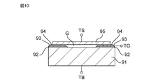
- FIG. 10 is a cross-sectional view showing an example of a conventional pressure sensor element.
- This pressure sensor element includes a conductive substrate 91 that functions as a base electrode, a membrane 95 that functions as a sense electrode, and a spacer portion that maintains a gap G between the two.
- the spacer portion includes a guard electrode layer 93 and electrically insulating layers 92 and 94 arranged above and below the guard electrode layer 93.
- a positive voltage or a negative voltage is applied between the base terminal TB and the sense terminal TS at regular intervals, and the generated charge is taken out and A / D (A / D). (Analog / digital) conversion is performed, and then linearity and temperature characteristics are corrected by digital calculation to convert to an appropriate pressure value.
- the reference capacitance electrode 6 is deformed by arranging a substantially C-shaped reference capacitance electrode 6 on the outside of the circular main capacitance electrode 5 and installing an insulating spacer 3b between the two. Is suppressed.
- the pressure sensor element shown in FIG. 10 is generally manufactured and shipped at a factory, and then mounted on a circuit board by soldering such as reflow in a product assembly line. At this time, heat is applied during mounting, and stress strain is generated in the package and the sensor body. As a result, the output offset of the pressure sensor may shift from the initial value by, for example, about 100 Pa, which contributes to the measurement error.
- An object of the present invention is to provide a pressure sensor element capable of achieving high measurement accuracy even after being mounted on a circuit board, and a pressure sensor module using the pressure sensor element.
- the present invention also provides a signal correction method for a pressure sensor module that can achieve high measurement accuracy even after being mounted on a circuit board.
- One aspect of the present invention is a pressure sensor element that detects a change in capacitance between electrodes.
- a sense electrode that constitutes a sense capacitor together with the base electrode and is deformable according to the ambient pressure difference, A spacer portion that maintains a gap between the base electrode portion and the sense electrode portion, and a spacer portion.
- a monitor capacitor is formed together with the base electrode portion, and a monitor electrode portion for detecting stress strain generated in the spacer portion is provided.
- a pressure sensor module comprising an integrated circuit for processing an output signal from the pressure sensor element.
- the integrated circuit includes a switching circuit that switches between the sense signal of the sense electrode portion and the monitor signal of the monitor electrode portion.
- An A / D converter that converts the output signal from the switching circuit into a digital signal
- a digital signal processing unit that performs signal processing on the digital signal, Includes a memory or register for storing the digital value of the monitor signal.
- Yet another aspect of the present invention is the signal correction method of the pressure sensor module described above.
- a step of measuring the capacitance of the monitor capacitor and storing it in a memory or a register as an initial capacitance value Before mounting the pressure sensor module on the circuit board, a step of measuring the capacitance of the monitor capacitor and storing it in a memory or a register as an initial capacitance value, and After mounting the pressure sensor module on the circuit board, the step of measuring the capacitance of the monitor capacitor and storing it in a memory or a register as a mounted capacitance value, and A step of calculating the distortion correction coefficient based on the initial capacitance value and the mounted capacitance value, and It includes a step of measuring the capacitance of the sense capacitor, correcting it using the strain correction coefficient, and then converting it into a pressure value.
- FIG. 1A is a plan view showing an example of the pressure sensor element according to the first embodiment of the present invention
- FIG. 1B is a sectional view thereof.
- It is an equivalent circuit diagram of the pressure sensor element shown in FIG.
- It is a circuit diagram which shows the electrical connection between a pressure sensor element and an integrated circuit.
- It is a block diagram which shows an example of an integrated circuit.
- It is a flowchart which shows an example of the operation sequence of an integrated circuit in a manufacturing stage.
- It is a flowchart which shows an example of the operation sequence of an integrated circuit after mounting on a circuit board.
- It is a top view which shows an example of the pressure sensor element 1 which concerns on Embodiment 2 of this invention.
- One aspect of the present invention is a pressure sensor element that detects a change in capacitance between electrodes.
- a sense electrode that constitutes a sense capacitor together with the base electrode and is deformable according to the ambient pressure difference, A spacer portion that maintains a gap between the base electrode portion and the sense electrode portion, and a spacer portion.
- a monitor capacitor is formed together with the base electrode portion, and a monitor electrode portion for detecting stress strain generated in the spacer portion is provided.
- the monitor electrode portion can detect the stress strain applied to the spacer portion. Therefore, when the pressure sensor element is mounted on the circuit board, even if the capacitance of the sense capacitor fluctuates due to thermal stress such as soldering, the change before and after mounting the capacitance of the monitor capacitor By taking this into consideration, it becomes possible to correct the capacitance of the sense capacitor to an appropriate value. As a result, the pressure value can be measured with high accuracy while being incorporated in the final product.
- the sense electrode portion includes a sense electrode having a rectangular or oval planar shape. It is preferable that the monitor electrode portion includes first, second, third and fourth monitor electrodes arranged on the left and right outer sides and the upper and lower outer sides from the sense electrode, respectively.
- the first, second, third and fourth monitor electrodes can individually detect stress strains generated on the left and right outer sides and the upper and lower outer sides of the sense electrode. Therefore, the state of stress strain can be detected more accurately.
- the sense electrode portion has a rectangular or oval planar shape and has a planar shape. It is preferable that the monitor electrode portion includes first and second monitor electrodes arranged on the left and right outer sides or the upper and lower outer sides from the sense electrode, respectively.
- the first and second monitor electrodes can individually detect stress strains generated on the left and right outer sides or the upper and lower outer sides of the sense electrode. Therefore, the state of stress strain can be detected more accurately with a simplified configuration.
- the monitor gap included in the monitor capacitor is fluidly isolated from the sense gap included in the sense capacitor.
- a pressure sensor module comprising an integrated circuit for processing an output signal from the pressure sensor element.
- the integrated circuit includes a switching circuit that switches between the sense signal of the sense electrode portion and the monitor signal of the monitor electrode portion.
- An A / D converter that converts the output signal from the switching circuit into a digital signal,
- a digital signal processing unit that performs signal processing on the digital signal,
- a memory or a register for storing a digital value of the monitor signal is included.
- Yet another aspect of the present invention is the signal correction method of the pressure sensor module described above.
- a step of measuring the capacitance of the monitor capacitor and storing it in a memory or a register as an initial capacitance value Before mounting the pressure sensor module on the circuit board, a step of measuring the capacitance of the monitor capacitor and storing it in a memory or a register as an initial capacitance value, and After mounting the pressure sensor module on the circuit board, the step of measuring the capacitance of the monitor capacitor and storing it in a memory or a register as a mounted capacitance value, and A step of calculating the distortion correction coefficient based on the initial capacitance value and the mounted capacitance value, and It includes a step of measuring the capacitance of the sense capacitor, correcting it using the strain correction coefficient, and then converting it into a pressure value.
- the distortion correction coefficient is calculated based on the initial capacitance value before mounting on the circuit board and the mounting capacitance value after mounting. Therefore, high measurement accuracy can be realized even after mounting on a circuit board. Moreover, since signal processing is performed in the module, the load on the external host can be reduced.
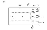
- FIG. 1A is a plan view showing an example of the pressure sensor element 1 according to the first embodiment of the present invention
- FIG. 1B is a sectional view thereof.
- the pressure sensor element 1 includes an electrically insulating substrate 10, a base electrode layer 20, spacer portions 30 and 31, a guard electrode layer 30A, a membrane plate 40, and the like.
- the substrate 10 is formed of an electrically insulating material such as silicon oxide.
- a base electrode layer 20 is provided on one main surface side of the substrate 10.
- the base electrode layer 20 functions as a base electrode portion that is a common electrode of the element 1, and is formed of, for example, a conductive material such as polycrystalline Si, amorous Si, or single crystal Si (those having a low resistivity).
- the substrate 10 may be formed of a conductive material to function as a base electrode portion. In that case, the base electrode layer 20 is unnecessary.
- the membrane plate 40 is formed of an electrically insulating material such as silicon oxide or single crystal silicon, and a sense electrode S and monitor electrodes M1 to M4 are installed on the lower surface thereof so as to face the substrate 10.
- a sense terminal TS, a base terminal TB, a guard terminal TG, and monitor terminals TM1 to TM4 are installed on the upper surface of the membrane plate 40.
- the sense terminal TS is electrically connected to the sense electrode S
- the base terminal TB is electrically connected to the upper surface of the base electrode layer 20
- the guard terminal TG is electrically connected to the guard electrode layer 30A
- the monitor terminals TM1 to The TM4 is electrically connected to the monitor electrodes M1 to M4, respectively.
- the sense electrode S has, for example, a rectangular planar shape, and constitutes a sense capacitor together with the upper surface of the base electrode layer 20 as a sense electrode portion.
- the spacer portions 30 and 31 are formed of an electrically insulating material such as silicon oxide, and have a gap G between the sense electrode S and the substrate 10 and a gap G1 to between the monitor electrodes M1 to M4 and the substrate 10. It is provided to maintain G4. In FIG. 1B, only the gaps G2 and G4 are shown.
- the spacer portion 30 is airtightly installed along the outer periphery of the substrate 10 so as to seal the gap G and the gaps G1 to G4.
- the spacer portion 31 is airtightly installed along the outer periphery of the sense electrode S so as to seal the gap G and the gaps G1 to G4.
- the gap G and the gaps G1 to G4 are spaces sealed from the outside and are fluidly isolated from each other (non-communication), for example, the inert gas is sealed and maintained at a constant pressure. Further, a dielectric material may be enclosed.
- the guard electrode layer 30A is provided inside the spacer portion 30. That is, the guard electrode layer 30A is provided along the outer periphery of the substrate 10 and is electrically insulated from the base electrode layer 20 and the membrane plate 40 by the spacer portion 30. By interposing the spacer portion 30 between the base electrode layer 20 and the membrane plate 40, a floating capacitance that is not related to the pressure change is generated. However, the floating capacitance can be canceled by electrically grounding the guard electrode layer 30A via the guard terminal TG.
- the monitor electrodes M1 to M4 have, for example, a rectangular planar shape, and form a monitor capacitor together with the substrate 10 as a monitor electrode portion. Since the width dimension of the gap G1 to G4 is smaller than the width dimension of the gap G, for example, the ratio is 1/4 to 1/10, the membrane plate 40 is elastically deformed according to the pressure difference between the external environment and the gap G. Even in this case, the monitor electrodes M1 to M4 are not displaced.
- the gaps G1 to G4 may be filled with a dielectric material different from the dielectric constant of the gap G, for example, a solid polymer, whereby deformation of the monitor electrodes M1 to M4 can be further suppressed.
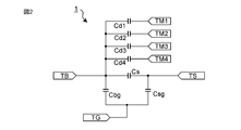
- FIG. 2 is an equivalent circuit diagram of the pressure sensor element 1 shown in FIG.
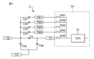
- FIG. 3 is a circuit diagram showing an electrical connection between the pressure sensor element 1 and the integrated circuit 50.
- a sense capacitor having a capacitance of Cs exists between the base terminal TB and the sense terminal TS.
- Monitor capacitors having capacitances Cd1 to Cd4 exist between the base terminal TB and the monitor terminals TM1 to TM4, respectively.
- a floating capacitance Cbg exists between the base terminal TB and the guard terminal TG.
- a floating capacitance Csg exists between the sense terminal TS and the guard terminal TG.
- the integrated circuit 50 is provided with switching circuits SW0 to SW4 and a CDC circuit 51 (CDC is an abbreviation for Capacitance to Digital Converter).
- the switching circuits SW0 to SW4 operate as a multiplexer that selects one output signal from a plurality of input signals at a predetermined timing. Specifically, a) When SW0 is on and SW1 to SW4 are off, the capacitance Cs can be detected. b) When SW1 is on and SW0, 2 to 4 are off, the capacitance Cd1 can be detected. c) When SW2 is on and SW0 to 1,3 to 4 are off, the capacitance Cd2 can be detected. d) When SW3 is on and SW0 to 2,4 are off, the capacitance Cd3 can be detected. e) When SW4 is on and SW0 to 3 are off, the capacitance Cd4 can be detected.
- the CDC circuit 51 includes an A / D converter that converts an analog signal into a digital signal, and converts the capacitance selected by the switching circuits SW0 to SW4 into a digital signal. Although not shown, between the switching circuits SW0 to SW4 and the CDC circuit 51, a pulse generator that supplies a square wave voltage to the capacitance and an amplifier that amplifies the charge generated from the capacitance are provided. Is provided.
- FIG. 4 is a block diagram showing an example of the integrated circuit 50.
- the integrated circuit 50 is composed of, for example, an ASIC, FPGA, PLD, CPLD, or the like, and includes the above-mentioned CDC circuit 51, a digital filter 52, a temperature sensor 53, a digital correction unit 54, a register 55, and a FIFO buffer 56. , Digital I / F (interface) 57 and the like. These can be implemented by a combination of an arithmetic processor such as a CPU and a GPU, a memory such as an EEPROM and a RAM, software, and hardware.
- the digital filter 52 filters the digital signal from the CDC circuit 51, removes high frequency noise components, and outputs a low frequency band signal.
- the temperature sensor 53 includes a PN junction diode, a thermistor, and the like, measures the temperature in the vicinity of the pressure sensor element 1, and outputs it as a digital value.
- the digital correction unit 54 corrects the digital pressure value output from the digital filter 52 by using the digital temperature value from the temperature sensor 53 and the correction coefficient stored in the internal memory, and performs temperature correction and linearity correction.
- the register 55 has a function of storing various digital data.
- the FIFO buffer 56 has a function of temporarily storing digital data and adjusting the timing of input and output.
- the digital I / F57 has a function of communicating with an external host and transmits / receives various digital data.
- the pressure sensor module includes such a pressure sensor element 1 and an integrated circuit 50.
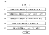
- FIG. 5 is a flowchart showing an example of the operation sequence of the integrated circuit 50 at the manufacturing stage.
- Such a sequence can be automatically operated, for example, by programming in a state machine (a digital circuit that automatically controls an operation procedure) in an ASIC.
- a state machine a digital circuit that automatically controls an operation procedure
- the initial values of the capacitances Cd1 to Cd4 of the monitor capacitors corresponding to the monitor electrodes M1 to M4 are measured.
- step P1 SW1 of the switching circuit is turned on, SW0 and SW2-4 are turned off, and the initial capacitance Cdi1 is measured.
- step P2 SW2 of the switching circuit is turned on, SW0 to 1 and SW3 to 4 are turned off, and the initial capacitance Cdi2 is measured.
- step P3 of the switching circuit is turned on, SW0 to SW2 and SW4 are turned off, and the initial capacitance Cdi3 is measured.
- step P4 of the switching circuit is turned on, SW0 to 3 are turned off, and the initial capacitance Cdi4 is measured.
- step P5 the measured initial capacities Cdi1 to Cdi4 are stored in the non-volatile memory or register of the integrated circuit 50, for example, EEPROM. At this stage, the pressure sensor module is ready for shipment.
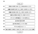
- FIG. 6 is a flowchart showing an example of the operation sequence of the integrated circuit 50 after mounting on the circuit board.
- a sequence can be automatically operated, for example, by programming into a state machine in the ASIC, and is started after the integrated circuit 50 is powered on or by receiving a control command from an external host.
- data correction is performed using the initial capacities Cdi1 to Cdi4 measured at the manufacturing stage.
- step S1 of the switching circuit is turned on, SW0 and SW2 to 4 are turned off, the capacity Cd1 after mounting is measured, and stored in a memory or a register.
- step S2 of the switching circuit is turned on, SW0 to 1 and SW3 to 4 are turned off, the capacity Cd2 after mounting is measured, and stored in a memory or a register.
- step S3 of the switching circuit is turned on, SW0 to SW2 and SW4 are turned off, the capacity Cd3 after mounting is measured, and stored in a memory or a register.
- step S4 of the switching circuit is turned on, SW0 to 3 are turned off, the capacity Cd4 after mounting is measured, and stored in a memory or a register.
- step S5 the initial capacities Cdi1 to Cdi4 stored in the memory or the register of the integrated circuit 50 are read out in step P5.
- step S6 the strain correction coefficient is calculated based on the initial capacitances Cdi1 to Cdi4 and the mounted capacitances Cd1 to Cd4 measured in steps S1 to S4.
- step S7 the obtained distortion correction coefficient is stored in the digital correction unit 54.
- step S8 digital correction is started.
- step S9 SW0 of the switching circuit is turned on, SW1 to SW4 are turned off, the current capacitance Cs is measured, and the pressure is converted into the pressure corrected using the distortion correction coefficient.
- the amount of change in the capacitance in the X direction / Y direction is calculated from the difference between the capacitances Cd1 and Cd3 and the capacitances Cd2 and Cd4 arranged so as to face each other via the sense electrode S.
- C ⁇ ⁇ S / d
- the displacement amounts dx and dy of the gaps G1 to G4 in the X direction / Y direction are calculated, and the following pressure fluctuation amount Offset is derived.
- ⁇ is a strain constant in the X direction
- ⁇ is a strain constant in the Y direction.
- Offset ⁇ ⁇ dx + ⁇ ⁇ dy... (1)
- FIG. 7 is a plan view showing an example of the pressure sensor element 1 according to the second embodiment of the present invention.
- the sense electrode S has an elliptical (or elliptical) planar shape as compared with the configuration of FIG. 1, and the monitor electrodes M1 to M4 also have an elliptical planar shape.
- the mechanical and electrical configurations are the same as those in FIG. Even in such a configuration, the monitor electrodes M1 to M4 can detect the stress strain applied to the spacer portion.
- FIG. 8 is a plan view showing an example of the pressure sensor element 1 according to the third embodiment of the present invention.
- the monitor electrodes M2 and M4 arranged on the left and right outer sides (short side side) from the sense electrode S are omitted, and only the two monitor electrodes M1 and M3 are separated from the sense electrode S. It is placed on the top, bottom, outside (long side).
- the mechanical and electrical configurations are the same as those in FIG. Even in such a configuration, the monitor electrodes M1 and M3 can detect the stress strain applied to the spacer portion.
- FIG. 9 is a plan view showing an example of the pressure sensor element 1 according to the fourth embodiment of the present invention.
- the monitor electrodes M1 and M3 arranged on the upper and lower outer sides (long side side) from the sense electrode S are omitted, and only the two monitor electrodes M2 and M4 are separated from the sense electrode S. It is located on the left and right outside (short side).
- the mechanical and electrical configurations are the same as those in FIG. Even in such a configuration, the monitor electrodes M2 and M4 can detect the stress strain applied to the spacer portion.
- planar shape of the sense electrode and the monitor electrode is a rectangular shape or an oval shape
- a polygonal shape such as a triangle, a pentagon, or a hexagon is also possible.
- the present invention is extremely useful in industry because it can realize high measurement accuracy even after being mounted on a circuit board.
Landscapes
- Physics & Mathematics (AREA)
- General Physics & Mathematics (AREA)
- Engineering & Computer Science (AREA)
- Microelectronics & Electronic Packaging (AREA)
- Power Engineering (AREA)
- Measuring Fluid Pressure (AREA)
Abstract
本発明は、電極間の静電容量の変化を検知する圧力センサ素子に関する。圧力センサ素子1は、電気絶縁性の基板10と、ベース電極層20と、スペーサ部30,31と、ガード電極層30Aと、メンブレンプレート40などを備える。メンブレンプレート40には、センス電極部としてのセンス電極Sおよびモニタ電極部としてのモニタ電極M1~M4が基板10と対向するように設置される。モニタ電極M1~M4は、回路基板に実装された場合にスペーサ部30,31に生ずる応力歪みを検知する。 こうした構成により、回路基板に実装した後でも高い測定精度を実現できる。
Description
本発明は、気圧や水圧などの圧力を測定するための圧力センサ素子およびそれを用いた圧力センサモジュールに関する。また本発明は、圧力センサモジュールの信号補正方法に関する。
圧力センサは、半導体製造技術を応用したMEMS(マイクロ電気機械システム)技術を用いて製造でき、例えば、約0.5~2mm角の超小型センサが実現できる。典型的な圧力センサは、2つの電極を備えたキャパシタ構造を有し、周囲圧力の変化に起因した静電容量の変化を検知することによって圧力測定が可能である。
図10は、従来の圧力センサ素子の一例を示す断面図である。この圧力センサ素子は、ベース電極として機能する導電性の基板91と、センス電極として機能するメンブレン95と、両者間に間隙Gを維持するスペーサ部とを備える。スペーサ部は、ガード電極層93と、上下に配置された電気絶縁層92,94とを含む。
基板91とメンブレン95との間の静電容量を測定する場合、ベース端子TBとセンス端子TSとの間に正電圧または負電圧を一定周期で印加し、発生する電荷を取り出してA/D(アナログ/デジタル)変換し、続いてデジタル演算によって直線性や温度特性を補正して適正な圧力値に変換している。
また下記の特許文献1では、円形状の主容量電極5の外側に略C字状の基準容量電極6を配置し、両者間に絶縁性スペーサ3bを設置することによって、基準容量電極6の変形を抑制している。
図10に示す圧力センサ素子は、一般に工場で製造され出荷された後、製品の組立てラインにおいてリフローなどのハンダ付けによって回路基板に実装される。このとき実装時に熱が印加され、パッケージやセンサ本体に応力歪みが発生する。その結果、圧力センサの出力オフセットとして、初期値から、例えば、100Pa程度シフトすることがあり、測定誤差の一因となる。
本発明の目的は、回路基板に実装した後でも高い測定精度を実現できる圧力センサ素子およびそれを用いた圧力センサモジュールを提供することである。また本発明は、回路基板に実装した後でも高い測定精度を実現できる圧力センサモジュールの信号補正方法を提供することである。
本発明の一態様は、電極間の静電容量の変化を検知する圧力センサ素子であって、
ベース電極部と、
該ベース電極部とともにセンスキャパシタを構成し、周囲圧力差に応じて変形可能であるセンス電極部と、
前記ベース電極部と前記センス電極部との間の間隙を維持するスペーサ部と、
前記ベース電極部とともにモニタキャパシタを構成し、該スペーサ部に生ずる応力歪みを検知するモニタ電極部と、を備える。
ベース電極部と、
該ベース電極部とともにセンスキャパシタを構成し、周囲圧力差に応じて変形可能であるセンス電極部と、
前記ベース電極部と前記センス電極部との間の間隙を維持するスペーサ部と、
前記ベース電極部とともにモニタキャパシタを構成し、該スペーサ部に生ずる応力歪みを検知するモニタ電極部と、を備える。
本発明の他の態様は、上記の圧力センサ素子と、
該圧力センサ素子からの出力信号を処理する集積回路と、を備える圧力センサモジュールであって、
該集積回路は、前記センス電極部のセンス信号と前記モニタ電極部のモニタ信号を切り替えるスイッチング回路と、
該スイッチング回路からの出力信号をデジタル信号に変換するA/Dコンバータと、
該デジタル信号に対して信号処理を行うデジタル信号処理部と、
前記モニタ信号のデジタル値を保存するためのメモリまたはレジスタと、を含む。
該圧力センサ素子からの出力信号を処理する集積回路と、を備える圧力センサモジュールであって、
該集積回路は、前記センス電極部のセンス信号と前記モニタ電極部のモニタ信号を切り替えるスイッチング回路と、
該スイッチング回路からの出力信号をデジタル信号に変換するA/Dコンバータと、
該デジタル信号に対して信号処理を行うデジタル信号処理部と、
前記モニタ信号のデジタル値を保存するためのメモリまたはレジスタと、を含む。
本発明のさらに他の態様は、上記の圧力センサモジュールの信号補正方法であって、
前記圧力センサモジュールを回路基板に実装する前に、前記モニタキャパシタの静電容量を測定し、初期容量値としてメモリまたはレジスタに保存するステップと、
前記圧力センサモジュールを回路基板に実装した後に、前記モニタキャパシタの静電容量を測定し、実装容量値としてメモリまたはレジスタに保存するステップと、
前記初期容量値および前記実装容量値に基づいて、歪み補正係数を計算するステップと、
前記センスキャパシタの静電容量を測定し、前記歪み補正係数を用いて補正した後、圧力値に換算するステップと、を含む。
前記圧力センサモジュールを回路基板に実装する前に、前記モニタキャパシタの静電容量を測定し、初期容量値としてメモリまたはレジスタに保存するステップと、
前記圧力センサモジュールを回路基板に実装した後に、前記モニタキャパシタの静電容量を測定し、実装容量値としてメモリまたはレジスタに保存するステップと、
前記初期容量値および前記実装容量値に基づいて、歪み補正係数を計算するステップと、
前記センスキャパシタの静電容量を測定し、前記歪み補正係数を用いて補正した後、圧力値に換算するステップと、を含む。
本発明によれば、回路基板に実装した後でも高い測定精度を実現できる。
本発明の一態様は、電極間の静電容量の変化を検知する圧力センサ素子であって、
ベース電極部と、
該ベース電極部とともにセンスキャパシタを構成し、周囲圧力差に応じて変形可能であるセンス電極部と、
前記ベース電極部と前記センス電極部との間の間隙を維持するスペーサ部と、
前記ベース電極部とともにモニタキャパシタを構成し、該スペーサ部に生ずる応力歪みを検知するモニタ電極部と、を備える。
ベース電極部と、
該ベース電極部とともにセンスキャパシタを構成し、周囲圧力差に応じて変形可能であるセンス電極部と、
前記ベース電極部と前記センス電極部との間の間隙を維持するスペーサ部と、
前記ベース電極部とともにモニタキャパシタを構成し、該スペーサ部に生ずる応力歪みを検知するモニタ電極部と、を備える。
この構成によれば、モニタ電極部は、スペーサ部に印加される応力歪みを検知することができる。そのため圧力センサ素子を回路基板に実装する際に、センスキャパシタの静電容量が、例えば、ハンダ付けなどの熱応力に起因して変動した場合でも、モニタキャパシタの静電容量の実装前後の変化を考慮することによって、センスキャパシタの静電容量を適切な値に補正することが可能になる。その結果、最終製品に組み込んだ状態で高精度の圧力値が測定できる。
前記センス電極部は、矩形状または長円形状の平面形状を有するセンス電極を含み、
前記モニタ電極部は、前記センス電極から左右外側および上下外側にそれぞれ配置された第1、第2、第3および第4モニタ電極を含むことが好ましい。
前記モニタ電極部は、前記センス電極から左右外側および上下外側にそれぞれ配置された第1、第2、第3および第4モニタ電極を含むことが好ましい。
この構成によれば、第1、第2、第3および第4モニタ電極は、センス電極の左右外側および上下外側において生ずる応力歪みを個別に検知することができる。そのため応力歪みの状態をより正確に検知できる。
前記センス電極部は、矩形状または長円形状の平面形状を有し、
前記モニタ電極部は、前記センス電極から左右外側または上下外側にそれぞれ配置された第1および第2モニタ電極を含むことが好ましい。
前記モニタ電極部は、前記センス電極から左右外側または上下外側にそれぞれ配置された第1および第2モニタ電極を含むことが好ましい。
この構成によれば、第1および第2モニタ電極は、センス電極の左右外側または上下外側において生ずる応力歪みを個別に検知することができる。そのため簡略化した構成で応力歪みの状態をより正確に検知できる。
前記モニタキャパシタに含まれるモニタ間隙は、前記センスキャパシタに含まれるセンス間隙から流体的に隔離されていることが好ましい。
この構成によれば、モニタキャパシタの容量測定とセンスキャパシタの容量測定との相互影響を低減できる。
本発明の他の態様は、上記の圧力センサ素子と、
該圧力センサ素子からの出力信号を処理する集積回路と、を備える圧力センサモジュールであって、
該集積回路は、前記センス電極部のセンス信号と前記モニタ電極部のモニタ信号を切り替えるスイッチング回路と、
該スイッチング回路からの出力信号をデジタル信号に変換するA/Dコンバータと、
該デジタル信号に対して信号処理を行うデジタル信号処理部と、
前記モニタ信号のデジタル値を保存するためのメモリまたはレジスタとを、含む。
該圧力センサ素子からの出力信号を処理する集積回路と、を備える圧力センサモジュールであって、
該集積回路は、前記センス電極部のセンス信号と前記モニタ電極部のモニタ信号を切り替えるスイッチング回路と、
該スイッチング回路からの出力信号をデジタル信号に変換するA/Dコンバータと、
該デジタル信号に対して信号処理を行うデジタル信号処理部と、
前記モニタ信号のデジタル値を保存するためのメモリまたはレジスタとを、含む。
この構成によれば、回路基板に実装した後でも高い測定精度を実現できる。またモジュール内で信号処理が可能になるため、外部ホストの負荷を軽減できる。
本発明のさらに他の態様は、上記の圧力センサモジュールの信号補正方法であって、
前記圧力センサモジュールを回路基板に実装する前に、前記モニタキャパシタの静電容量を測定し、初期容量値としてメモリまたはレジスタに保存するステップと、
前記圧力センサモジュールを回路基板に実装した後に、前記モニタキャパシタの静電容量を測定し、実装容量値としてメモリまたはレジスタに保存するステップと、
前記初期容量値および前記実装容量値に基づいて、歪み補正係数を計算するステップと、
前記センスキャパシタの静電容量を測定し、前記歪み補正係数を用いて補正した後、圧力値に換算するステップと、を含む。
前記圧力センサモジュールを回路基板に実装する前に、前記モニタキャパシタの静電容量を測定し、初期容量値としてメモリまたはレジスタに保存するステップと、
前記圧力センサモジュールを回路基板に実装した後に、前記モニタキャパシタの静電容量を測定し、実装容量値としてメモリまたはレジスタに保存するステップと、
前記初期容量値および前記実装容量値に基づいて、歪み補正係数を計算するステップと、
前記センスキャパシタの静電容量を測定し、前記歪み補正係数を用いて補正した後、圧力値に換算するステップと、を含む。
この構成によれば、回路基板に実装する前の初期容量値および実装した後の実装容量値に基づいて、歪み補正係数を計算する。そのため回路基板に実装した後でも高い測定精度を実現できる。またモジュール内で信号処理を行うため、外部ホストの負荷を軽減できる。
(実施形態1)
図1(A)は本発明の実施形態1に係る圧力センサ素子1の一例を示す平面図であり、図1(B)はその断面図である。
図1(A)は本発明の実施形態1に係る圧力センサ素子1の一例を示す平面図であり、図1(B)はその断面図である。
圧力センサ素子1は、電気絶縁性の基板10と、ベース電極層20と、スペーサ部30,31と、ガード電極層30Aと、メンブレンプレート40などを備える。
基板10は、酸化シリコンなどの電気絶縁性の材料で形成される。基板10の一方主面側にはベース電極層20が設けられる。ベース電極層20は、素子1のコモン電極であるベース電極部として機能し、例えば、多結晶Si、アモルアァスSi、単結晶Si(抵抗率が低いもの)などの導電性材料で形成される。代替として、基板10を導電性材料で形成してベース電極部として機能させてもよい。その場合、ベース電極層20は不要である。
メンブレンプレート40は、酸化シリコン、単結晶シリコンなどの電気絶縁性の材料で形成され、その下面にはセンス電極Sおよびモニタ電極M1~M4が基板10と対向するように設置される。メンブレンプレート40の上面には、センス端子TS、ベース端子TB、ガード端子TG、モニタ端子TM1~TM4が設置される。センス端子TSはセンス電極Sと電気的に接続され、ベース端子TBはベース電極層20の上面と電気的に接続され、ガード端子TGはガード電極層30Aと電気的に接続され、モニタ端子TM1~TM4はそれぞれモニタ電極M1~M4と電気的に接続される。
センス電極Sは、例えば、矩形状の平面形状を有しており、センス電極部として、ベース電極層20の上面とともにセンスキャパシタを構成する。電極間の静電容量Csは、間隙Gの誘電率ε、電極面積S、電極間距離dを用いて、Cs=ε×S/dで表される。外部と間隙Gとの圧力差に応じてメンブレンプレート40が弾性変形すると、センス電極Sの変位により電極間距離dが変化し、それに応じて静電容量Csも変化する。静電容量Csの変化は、センス端子TSを経由して外部回路によって検出される。
スペーサ部30,31は、酸化シリコンなどの電気絶縁性の材料で形成され、センス電極Sと基板10との間の間隙G、および各モニタ電極M1~M4と基板10との間の間隙G1~G4を維持するために設けられる。なお、図1(B)では間隙G2,G4だけを図示している。スペーサ部30は、基板10の外周に沿って間隙Gおよび間隙G1~G4を封止するように気密的に設置される。スペーサ部31は、センス電極Sの外周に沿って間隙Gおよび間隙G1~G4を封止するように気密的に設置される。間隙Gおよび間隙G1~G4は、外部から密閉された空間であり、そして互いに流体的に隔離されており(非連通)、例えば、不活性ガスが封入されて一定の圧力に維持される。また、誘電体材料を封入してもよい。
ガード電極層30Aは、スペーサ部30の内部に設けられる。すなわち、ガード電極層30Aは、基板10の外周に沿って設けられ、スペーサ部30によってベース電極層20およびメンブレンプレート40から電気的に絶縁されている。スペーサ部30がベース電極層20とメンブレンプレート40との間に介在することにより、圧力変化に関係しない浮遊静電容量が発生する。しかし、ガード端子TGを介して、ガード電極層30Aを電気的に接地することにより、浮遊静電容量をキャンセルすることが可能になる。
モニタ電極M1~M4は、例えば、矩形状の平面形状を有しており、モニタ電極部として、基板10とともにモニタキャパシタを構成する。間隙G1~G4の幅寸法は間隙Gの幅寸法より小さく、例えば、1/4~1/10の比率であるため、外部環境と間隙Gとの圧力差に応じてメンブレンプレート40が弾性変形した場合でも、モニタ電極M1~M4は変位しない。間隙G1~G4には、間隙Gの誘電率とは異なる誘電体、例えば、固体ポリマーで充填してもよく、これによりモニタ電極M1~M4の変形をさらに抑制できる。
一方、圧力センサ素子1がリフローなどのハンダ付けによって回路基板に実装された場合、熱に起因してスペーサ部30,31に応力歪みが発生し、電極間距離dが僅かに変動することがある。このとき各モニタ電極M1~M4に対応するモニタキャパシタの静電容量Cd1~Cd4が応力歪み分布に応じて変化するため、スペーサ部31に生ずる応力歪みを検知することが可能である。静電容量Cd1~Cd4の変化は、モニタ端子TM1~TM4を経由して外部回路によってそれぞれ検出される。
図2は、図1に示す圧力センサ素子1の等価回路図である。図3は、圧力センサ素子1と集積回路50との電気接続を示す回路図である。ベース端子TBとセンス端子TSとの間には、静電容量Csのセンスキャパシタが存在する。ベース端子TBとモニタ端子TM1~TM4との間には、静電容量Cd1~Cd4のモニタキャパシタがそれぞれ存在する。ベース端子TBとガード端子TGとの間には、浮遊静電容量Cbgが存在する。センス端子TSとガード端子TGとの間には、浮遊静電容量Csgが存在する。
図3に示すように、集積回路50には、スイッチング回路SW0~SW4と、CDC回路51とが設けられる(CDCはCapacitance to Digital Convertorの略称)。スイッチング回路SW0~SW4は、複数の入力信号の中から1つの出力信号を所定のタイミングで選択するマルチプレクサとして動作する。具体的には、a)SW0がオンで、SW1~4がオフの場合、静電容量Csが検出できる。b)SW1がオンで、SW0,2~4がオフの場合、静電容量Cd1が検出できる。c)SW2がオンで、SW0~1,3~4がオフの場合、静電容量Cd2が検出できる。d)SW3がオンで、SW0~2,4がオフの場合、静電容量Cd3が検出できる。e)SW4がオンで、SW0~3がオフの場合、静電容量Cd4が検出できる。
CDC回路51は、アナログ信号をデジタル信号に変換するA/Dコンバータを含み、スイッチング回路SW0~SW4によって選択された静電容量をデジタル信号に変換する。なお、図示していないが、スイッチング回路SW0~SW4とCDC回路51との間には、静電容量に矩形波電圧を供給するパルス発生器と、静電容量から発生した電荷を増幅する増幅器とが設けられる。
図4は、集積回路50の一例を示すブロック図である。集積回路50は、例えば、ASIC、FPGA、PLD、CPLDなどで構成され、上述したCDC回路51と、デジタルフィルタ52と、温度センサ53と、デジタル補正部54と、レジスタ55と、FIFOバッファ56と、デジタルI/F(インタフェース)57などで構成される。これらはCPU、GPUなどの演算プロセッサ、EEPROM、RAMなどのメモリ、ソフトウエア、ハードウエアの組合せで実装できる。
デジタルフィルタ52は、CDC回路51からのデジタル信号に対してフィルタリングを施し、高域周波数のノイズ成分を除去し、低域周波数帯の信号を出力する。温度センサ53は、PN接合ダイオードやサーミスタなどを含み、圧力センサ素子1近傍の温度を測定してデジタル値として出力する。
デジタル補正部54は、温度センサ53からのデジタル温度値および内部メモリで保存された補正係数を用いて、デジタルフィルタ52から出力されるデジタル圧力値を補正し、温度補正と直線性補正を行う。レジスタ55は、各種デジタルデータを保存する機能を有する。FIFOバッファ56は、デジタルデータを一時的に保存して、入力と出力のタイミングを調整する機能を有する。デジタルI/F57は、外部ホストと通信する機能を有し、各種デジタルデータの送受信を行う。
圧力センサモジュールは、こうした圧力センサ素子1および集積回路50を備える。
図5は、製造段階での集積回路50の動作シーケンスの一例を示すフローチャートである。こうしたシーケンスは、例えば、ASIC内のステートマシン(動作手順を自動制御するデジタル回路)にプログラミングすることによって自動的に動作可能である。ここでは、モニタ電極M1~M4に対応するモニタキャパシタの静電容量Cd1~Cd4の初期値を測定する。
最初にステップP1において、スイッチング回路のSW1をオン、SW0とSW2~4をオフにして、初期容量Cdi1を測定する。次にステップP2において、スイッチング回路のSW2をオン、SW0~1とSW3~4をオフにして、初期容量Cdi2を測定する。
次にステップP3において、スイッチング回路のSW3をオン、SW0~2とSW4をオフにして、初期容量Cdi3を測定する。次にステップP4において、スイッチング回路のSW4をオン、SW0~3をオフにして、初期容量Cdi4を測定する。
次にステップP5において、測定した初期容量Cdi1~Cdi4を集積回路50の不揮発性メモリまたはレジスタ、例えば、EEPROMに保存する。この段階で圧力センサモジュールは出荷できる状態になる。
図6は、回路基板への実装後での集積回路50の動作シーケンスの一例を示すフローチャートである。こうしたシーケンスは、例えば、ASIC内のステートマシンにプログラミングすることによって自動的に動作可能であり、集積回路50の電源投入後または外部ホストからの制御コマンドを受信することによってスタートする。ここでは、製造段階で測定した初期容量Cdi1~Cdi4を用いてデータ補正を行う。
最初にステップS1において、スイッチング回路のSW1をオン、SW0とSW2~4をオフにして、実装後の容量Cd1を測定し、メモリまたはレジスタに保存する。次にステップS2において、スイッチング回路のSW2をオン、SW0~1とSW3~4をオフにして、実装後の容量Cd2を測定し、メモリまたはレジスタに保存する。
次にステップS3において、スイッチング回路のSW3をオン、SW0~2とSW4をオフにして、実装後の容量Cd3を測定し、メモリまたはレジスタに保存する。次にステップS4において、スイッチング回路のSW4をオン、SW0~3をオフにして、実装後の容量Cd4を測定し、メモリまたはレジスタに保存する。
次にステップS5において、ステップP5で集積回路50のメモリまたはレジスタに保存した初期容量Cdi1~Cdi4を読み出す。次にステップS6において、初期容量Cdi1~Cdi4およびステップS1~S4で測定した実装後の容量Cd1~Cd4に基づいて、歪み補正係数を計算する。
次にステップS7において、得られた歪み補正係数をデジタル補正部54に保存する。次にステップS8において、デジタル補正をスタートする。
次にステップS9において、スイッチング回路のSW0をオン、SW1~4をオフにして、現在の容量Csを測定し、歪み補正係数を用いて補正された圧力に換算する。
一例として、歪み補正係数を計算する具体的な手法について説明する。まず差分ΔCdn=Cdn-Cdin(n=1,2,3,4)を算出する。次にセンス電極Sを介して対向配置されている容量Cd1,Cd3および容量Cd2,Cd4の差分から容量のX方向/Y方向の変化量を算出する。次にキャパシタに関する式:C=ε×S/dを用いて、間隙G1~G4のX方向/Y方向の変位量dx,dyを算出し、下記の圧力変動量Poffsetを導出する。なお、αはX方向に関する歪み定数、βはY方向に関する歪み定数である。
Poffset=α×dx+β×dy …(1)
Poffset=α×dx+β×dy …(1)
全ての容量値はデジタル化されたデータとして集積回路のメモリまたはレジスタに保存される。また温度センサ53からの温度値もデジタル化されて温度データとして使用できる。また温度特性および直線性は、製造段階で事前に取得した補正係数とともに多項式演算して、下記の最終出力p(L,T)が得られる。なお、aijは温度/直線性の補正係数、f(L)は直線性の関数、f(T)は温度の関数である。
p(L,T)=Σ[aij・f(L)・f(T)] …(2)
p(L,T)=Σ[aij・f(L)・f(T)] …(2)
応力歪み補正を考慮するために、前の手順で求めた圧力変動量Poffsetを式(2)から減算して、最終の圧力値Pfinalを得る。
Pfinal=p(L,T)-Poffset …(3)
Pfinal=p(L,T)-Poffset …(3)
これらの補正計算は、図4中のデジタル補正部54において内部クロックに同期して実行できる。
(実施形態2)
図7は、本発明の実施形態2に係る圧力センサ素子1の一例を示す平面図である。本実施形態では、図1の構成と比べて、センス電極Sは、長円(または楕円)形状の平面形状を有しおり、モニタ電極M1~M4も長円形状の平面形状を有している。これ以外の機械的および電気的な構成は図1のものと同様である。こうした構成においても、モニタ電極M1~M4は、スペーサ部に印加される応力歪みを検知できる。
図7は、本発明の実施形態2に係る圧力センサ素子1の一例を示す平面図である。本実施形態では、図1の構成と比べて、センス電極Sは、長円(または楕円)形状の平面形状を有しおり、モニタ電極M1~M4も長円形状の平面形状を有している。これ以外の機械的および電気的な構成は図1のものと同様である。こうした構成においても、モニタ電極M1~M4は、スペーサ部に印加される応力歪みを検知できる。
(実施形態3)
図8は、本発明の実施形態3に係る圧力センサ素子1の一例を示す平面図である。本実施形態では、図1の構成と比べて、センス電極Sから左右外側(短辺側)に配置されたモニタ電極M2,M4を省略し、2つのモニタ電極M1,M3だけをセンス電極Sから上下外側(長辺側)に配置している。これ以外の機械的および電気的な構成は図1のものと同様である。こうした構成においても、モニタ電極M1,M3は、スペーサ部に印加される応力歪みを検知できる。
図8は、本発明の実施形態3に係る圧力センサ素子1の一例を示す平面図である。本実施形態では、図1の構成と比べて、センス電極Sから左右外側(短辺側)に配置されたモニタ電極M2,M4を省略し、2つのモニタ電極M1,M3だけをセンス電極Sから上下外側(長辺側)に配置している。これ以外の機械的および電気的な構成は図1のものと同様である。こうした構成においても、モニタ電極M1,M3は、スペーサ部に印加される応力歪みを検知できる。
(実施形態4)
図9は、本発明の実施形態4に係る圧力センサ素子1の一例を示す平面図である。本実施形態では、図1の構成と比べて、センス電極Sから上下外側(長辺側)に配置されたモニタ電極M1,M3を省略し、2つのモニタ電極M2,M4だけをセンス電極Sから左右外側(短辺側)に配置している。これ以外の機械的および電気的な構成は図1のものと同様である。こうした構成においても、モニタ電極M2,M4は、スペーサ部に印加される応力歪みを検知できる。
図9は、本発明の実施形態4に係る圧力センサ素子1の一例を示す平面図である。本実施形態では、図1の構成と比べて、センス電極Sから上下外側(長辺側)に配置されたモニタ電極M1,M3を省略し、2つのモニタ電極M2,M4だけをセンス電極Sから左右外側(短辺側)に配置している。これ以外の機械的および電気的な構成は図1のものと同様である。こうした構成においても、モニタ電極M2,M4は、スペーサ部に印加される応力歪みを検知できる。
以上の実施形態では、センス電極の周囲に4つまたは2つのモニタ電極を配置する場合を説明したが、それ以外に1つ、3つまたは5つのモニタ電極を配置することも可能である。
また以上の実施形態では、センス電極およびモニタ電極の平面形状が矩形状または長円形状である場合を説明したが、それ以外に三角形、五角形、六角形などの多角形も可能である。
本発明は、添付図面を参照しながら好ましい実施形態に関連して充分に記載されているが、この技術の熟練した人々にとっては種々の変形や修正は明白である。そのような変形や修正は、添付した請求の範囲による本発明の範囲から外れない限りにおいて、その中に含まれると理解されるべきである。
本発明は、回路基板に実装した後でも高い測定精度を実現できるため、産業上極めて有用である。
1 圧力センサ素子
10 基板
20 ベース電極層
30,31 スペーサ部
30A ガード電極層
40 メンブレンプレート
50 集積回路
51 CDC回路
52 デジタルフィルタ
53 温度センサ
54 デジタル補正部
55 レジスタ
56 FIFOバッファ
57 デジタルI/F
G 間隙
M1~M4 モニタ電極
S センス電極
SW0~SW4 スイッチング回路
TS センス端子
TB ベース端子
TG ガード端子
TM1~TM4 モニタ端子
10 基板
20 ベース電極層
30,31 スペーサ部
30A ガード電極層
40 メンブレンプレート
50 集積回路
51 CDC回路
52 デジタルフィルタ
53 温度センサ
54 デジタル補正部
55 レジスタ
56 FIFOバッファ
57 デジタルI/F
G 間隙
M1~M4 モニタ電極
S センス電極
SW0~SW4 スイッチング回路
TS センス端子
TB ベース端子
TG ガード端子
TM1~TM4 モニタ端子
Claims (6)
- 電極間の静電容量の変化を検知する圧力センサ素子であって、
ベース電極部と、
該ベース電極部とともにセンスキャパシタを構成し、周囲圧力差に応じて変形可能であるセンス電極部と、
前記ベース電極部と前記センス電極部との間の間隙を維持するスペーサ部と、
前記ベース電極部とともにモニタキャパシタを構成し、該スペーサ部に生ずる応力歪みを検知するモニタ電極部と、を備える圧力センサ素子。 - 前記センス電極部は、矩形状または長円形状の平面形状を有するセンス電極を含み、
前記モニタ電極部は、前記センス電極から左右外側および上下外側にそれぞれ配置された第1、第2、第3および第4モニタ電極を含む、請求項1に記載の圧力センサ素子。 - 前記センス電極部は、矩形状または長円形状の平面形状を有し、
前記モニタ電極部は、前記センス電極から左右外側または上下外側にそれぞれ配置された第1および第2モニタ電極を含む、請求項1に記載の圧力センサ素子。 - 前記モニタキャパシタに含まれるモニタ間隙は、前記センスキャパシタに含まれるセンス間隙から流体的に隔離されている、請求項1に記載の圧力センサ素子。
- 請求項1~4のいずれかに記載の圧力センサ素子と、
該圧力センサ素子からの出力信号を処理する集積回路と、を備える圧力センサモジュールであって、
該集積回路は、前記センス電極部のセンス信号と前記モニタ電極部のモニタ信号を切り替えるスイッチング回路と、
該スイッチング回路からの出力信号をデジタル信号に変換するA/Dコンバータと、
該デジタル信号に対して信号処理を行うデジタル信号処理部と、
前記モニタ信号のデジタル値を保存するためのメモリまたはレジスタと、を含む、圧力センサモジュール。 - 請求項5に記載の圧力センサモジュールの信号補正方法であって、
前記圧力センサモジュールを回路基板に実装する前に、前記モニタキャパシタの静電容量を測定し、初期容量値としてメモリまたはレジスタに保存するステップと、
前記圧力センサモジュールを回路基板に実装した後に、前記モニタキャパシタの静電容量を測定し、実装容量値としてメモリまたはレジスタに保存するステップと、
前記初期容量値および前記実装容量値に基づいて、歪み補正係数を計算するステップと、
前記センスキャパシタの静電容量を測定し、前記歪み補正係数を用いて補正した後、圧力値に換算するステップと、を含む圧力センサモジュールの信号補正方法。
Priority Applications (2)
| Application Number | Priority Date | Filing Date | Title |
|---|---|---|---|
| CN202180048158.4A CN115803598B (zh) | 2020-07-06 | 2021-06-11 | 压力传感器元件、压力传感器模块及其信号校正方法 |
| US18/086,710 US12306050B2 (en) | 2020-07-06 | 2022-12-22 | Pressure sensor device, pressure sensor module, and signal correction method for pressure sensor module |
Applications Claiming Priority (2)
| Application Number | Priority Date | Filing Date | Title |
|---|---|---|---|
| JP2020-116547 | 2020-07-06 | ||
| JP2020116547 | 2020-07-06 |
Related Child Applications (1)
| Application Number | Title | Priority Date | Filing Date |
|---|---|---|---|
| US18/086,710 Continuation US12306050B2 (en) | 2020-07-06 | 2022-12-22 | Pressure sensor device, pressure sensor module, and signal correction method for pressure sensor module |
Publications (1)
| Publication Number | Publication Date |
|---|---|
| WO2022009604A1 true WO2022009604A1 (ja) | 2022-01-13 |
Family
ID=79552492
Family Applications (1)
| Application Number | Title | Priority Date | Filing Date |
|---|---|---|---|
| PCT/JP2021/022241 Ceased WO2022009604A1 (ja) | 2020-07-06 | 2021-06-11 | 圧力センサ素子、圧力センサモジュールおよびその信号補正方法 |
Country Status (3)
| Country | Link |
|---|---|
| US (1) | US12306050B2 (ja) |
| CN (1) | CN115803598B (ja) |
| WO (1) | WO2022009604A1 (ja) |
Citations (1)
| Publication number | Priority date | Publication date | Assignee | Title |
|---|---|---|---|---|
| JP2815279B2 (ja) * | 1993-03-30 | 1998-10-27 | 本田技研工業株式会社 | 圧力センサー |
Family Cites Families (16)
| Publication number | Priority date | Publication date | Assignee | Title |
|---|---|---|---|---|
| JPH0666658A (ja) * | 1992-08-15 | 1994-03-11 | Stec Kk | 静電容量型圧力センサ |
| US5561247A (en) * | 1993-03-30 | 1996-10-01 | Honda Motor Co., Ltd. | Pressure sensor |
| JPH0961273A (ja) | 1995-08-28 | 1997-03-07 | Hokuriku Electric Ind Co Ltd | 静電容量式圧力センサ |
| WO1998012528A1 (fr) * | 1996-09-19 | 1998-03-26 | Hokuriku Electric Industry Co., Ltd. | Capteur de pression a capacite electrostatique |
| US5965821A (en) * | 1997-07-03 | 1999-10-12 | Mks Instruments, Inc. | Pressure sensor |
| JP3025468B2 (ja) * | 1997-11-06 | 2000-03-27 | 株式会社ワコー | 静電容量の変化を利用したセンサおよびその製造方法 |
| JP3362714B2 (ja) * | 1998-11-16 | 2003-01-07 | 株式会社豊田中央研究所 | 静電容量型圧力センサおよびその製造方法 |
| US7024947B2 (en) * | 2002-03-07 | 2006-04-11 | Alps Electric Co., Ltd. | Detection device including circuit component |
| JP4090939B2 (ja) * | 2002-05-29 | 2008-05-28 | ニッタ株式会社 | 静電容量式センサおよびその製造方法 |
| JP4706704B2 (ja) * | 2006-04-26 | 2011-06-22 | 株式会社村田製作所 | 角速度センサの温度特性設定方法および角速度センサ |
| CN100442036C (zh) * | 2006-04-28 | 2008-12-10 | 中国科学院合肥物质科学研究院 | 一种双电容厚膜陶瓷感压元件的制备方法 |
| DE102007019639A1 (de) * | 2007-04-26 | 2008-10-30 | Robert Bosch Gmbh | Mikromechanisches Bauelement und entsprechendes Herstellungsverfahren |
| DE102010001797B4 (de) * | 2010-02-11 | 2023-09-28 | Robert Bosch Gmbh | Mikromechanisches Sensorelement zur kapazitiven Differenzdruckerfassung |
| FI126999B (en) * | 2014-01-17 | 2017-09-15 | Murata Manufacturing Co | Improved pressure sensor |
| JP6654157B2 (ja) * | 2017-01-17 | 2020-02-26 | アズビル株式会社 | 圧力センサ |
| JP6708597B2 (ja) * | 2017-11-03 | 2020-06-10 | 俊 保坂 | センサ・デバイスおよびその製造方法 |
-
2021
- 2021-06-11 CN CN202180048158.4A patent/CN115803598B/zh active Active
- 2021-06-11 WO PCT/JP2021/022241 patent/WO2022009604A1/ja not_active Ceased
-
2022
- 2022-12-22 US US18/086,710 patent/US12306050B2/en active Active
Patent Citations (1)
| Publication number | Priority date | Publication date | Assignee | Title |
|---|---|---|---|---|
| JP2815279B2 (ja) * | 1993-03-30 | 1998-10-27 | 本田技研工業株式会社 | 圧力センサー |
Also Published As
| Publication number | Publication date |
|---|---|
| CN115803598B (zh) | 2025-09-30 |
| CN115803598A (zh) | 2023-03-14 |
| US20230130920A1 (en) | 2023-04-27 |
| US12306050B2 (en) | 2025-05-20 |
Similar Documents
| Publication | Publication Date | Title |
|---|---|---|
| US6051853A (en) | Semiconductor pressure sensor including reference capacitor on the same substrate | |
| KR100922091B1 (ko) | 용량식 압력센서 | |
| US7841239B2 (en) | Electrostatic capacitance diaphragm vacuum gauge and vacuum processing apparatus | |
| US9383284B2 (en) | Diaphragm-type pressure gauge | |
| USRE46486E1 (en) | Semiconductor pressure sensor | |
| JP4296731B2 (ja) | 静電容量型圧力センサの製造方法 | |
| US6586943B1 (en) | Sensor signal processing apparatus | |
| US20200200631A1 (en) | Micromechanical component for a capacitive pressure sensor device | |
| CN110174198B (zh) | 具有机械解耦的温度传感器的应变仪 | |
| US5969258A (en) | Evaluation unit of a differential-pressure sensor | |
| JP3399688B2 (ja) | 圧力センサ | |
| CA2305317A1 (en) | Micromechanical sensor and method for operating the sensor | |
| WO2022009604A1 (ja) | 圧力センサ素子、圧力センサモジュールおよびその信号補正方法 | |
| CN110114650B (zh) | 压力传感器元件和具备该压力传感器元件的压力传感器模块 | |
| JP3409980B2 (ja) | 半導体圧力センサ | |
| EP1653209A1 (en) | Quartz type pressure sensor, and production method therefor | |
| JP2005010021A (ja) | 差圧伝送器 | |
| CN111712697A (zh) | 压力计 | |
| US20220364945A1 (en) | Pressure sensor apparatus | |
| EP4345436A1 (en) | Notification sensor arrangement for a differential pressure sensor and a method for outputting a sensed warning signal | |
| JPH109979A (ja) | ドライタイプ圧力検出装置 | |
| US7367234B2 (en) | Pressure sensor | |
| JP5626502B2 (ja) | 応力検出装置 | |
| JP2025062339A (ja) | 信号出力装置、及び、その生産方法 | |
| JP2001082909A (ja) | 静電容量式歪センサ |
Legal Events
| Date | Code | Title | Description |
|---|---|---|---|
| 121 | Ep: the epo has been informed by wipo that ep was designated in this application |
Ref document number: 21837535 Country of ref document: EP Kind code of ref document: A1 |
|
| NENP | Non-entry into the national phase |
Ref country code: DE |
|
| 122 | Ep: pct application non-entry in european phase |
Ref document number: 21837535 Country of ref document: EP Kind code of ref document: A1 |
|
| NENP | Non-entry into the national phase |
Ref country code: JP |
|
| WWG | Wipo information: grant in national office |
Ref document number: 202180048158.4 Country of ref document: CN |