WO2022009482A1 - パワー半導体モジュール及び電力変換装置 - Google Patents
パワー半導体モジュール及び電力変換装置 Download PDFInfo
- Publication number
- WO2022009482A1 WO2022009482A1 PCT/JP2021/011484 JP2021011484W WO2022009482A1 WO 2022009482 A1 WO2022009482 A1 WO 2022009482A1 JP 2021011484 W JP2021011484 W JP 2021011484W WO 2022009482 A1 WO2022009482 A1 WO 2022009482A1
- Authority
- WO
- WIPO (PCT)
- Prior art keywords
- conductive pattern
- power semiconductor
- emitter
- gate
- semiconductor element
- Prior art date
- Legal status (The legal status is an assumption and is not a legal conclusion. Google has not performed a legal analysis and makes no representation as to the accuracy of the status listed.)
- Ceased
Links
Images






















Classifications
-
- H—ELECTRICITY
- H02—GENERATION; CONVERSION OR DISTRIBUTION OF ELECTRIC POWER
- H02M—APPARATUS FOR CONVERSION BETWEEN AC AND AC, BETWEEN AC AND DC, OR BETWEEN DC AND DC, AND FOR USE WITH MAINS OR SIMILAR POWER SUPPLY SYSTEMS; CONVERSION OF DC OR AC INPUT POWER INTO SURGE OUTPUT POWER; CONTROL OR REGULATION THEREOF
- H02M7/00—Conversion of AC power input into DC power output; Conversion of DC power input into AC power output
- H02M7/42—Conversion of DC power input into AC power output without possibility of reversal
- H02M7/44—Conversion of DC power input into AC power output without possibility of reversal by static converters
- H02M7/48—Conversion of DC power input into AC power output without possibility of reversal by static converters using discharge tubes with control electrode or semiconductor devices with control electrode
-
- H—ELECTRICITY
- H10—SEMICONDUCTOR DEVICES; ELECTRIC SOLID-STATE DEVICES NOT OTHERWISE PROVIDED FOR
- H10W—GENERIC PACKAGES, INTERCONNECTIONS, CONNECTORS OR OTHER CONSTRUCTIONAL DETAILS OF DEVICES COVERED BY CLASS H10
- H10W90/00—Package configurations
-
- H—ELECTRICITY
- H10—SEMICONDUCTOR DEVICES; ELECTRIC SOLID-STATE DEVICES NOT OTHERWISE PROVIDED FOR
- H10W—GENERIC PACKAGES, INTERCONNECTIONS, CONNECTORS OR OTHER CONSTRUCTIONAL DETAILS OF DEVICES COVERED BY CLASS H10
- H10W72/00—Interconnections or connectors in packages
- H10W72/851—Dispositions of multiple connectors or interconnections
- H10W72/853—On the same surface
- H10W72/865—Die-attach connectors and bond wires
-
- H—ELECTRICITY
- H10—SEMICONDUCTOR DEVICES; ELECTRIC SOLID-STATE DEVICES NOT OTHERWISE PROVIDED FOR
- H10W—GENERIC PACKAGES, INTERCONNECTIONS, CONNECTORS OR OTHER CONSTRUCTIONAL DETAILS OF DEVICES COVERED BY CLASS H10
- H10W72/00—Interconnections or connectors in packages
- H10W72/90—Bond pads, in general
- H10W72/921—Structures or relative sizes of bond pads
- H10W72/926—Multiple bond pads having different sizes
-
- H—ELECTRICITY
- H10—SEMICONDUCTOR DEVICES; ELECTRIC SOLID-STATE DEVICES NOT OTHERWISE PROVIDED FOR
- H10W—GENERIC PACKAGES, INTERCONNECTIONS, CONNECTORS OR OTHER CONSTRUCTIONAL DETAILS OF DEVICES COVERED BY CLASS H10
- H10W90/00—Package configurations
- H10W90/701—Package configurations characterised by the relative positions of pads or connectors relative to package parts
- H10W90/731—Package configurations characterised by the relative positions of pads or connectors relative to package parts of die-attach connectors
- H10W90/734—Package configurations characterised by the relative positions of pads or connectors relative to package parts of die-attach connectors between a chip and a stacked insulating package substrate, interposer or RDL
-
- H—ELECTRICITY
- H10—SEMICONDUCTOR DEVICES; ELECTRIC SOLID-STATE DEVICES NOT OTHERWISE PROVIDED FOR
- H10W—GENERIC PACKAGES, INTERCONNECTIONS, CONNECTORS OR OTHER CONSTRUCTIONAL DETAILS OF DEVICES COVERED BY CLASS H10
- H10W90/00—Package configurations
- H10W90/701—Package configurations characterised by the relative positions of pads or connectors relative to package parts
- H10W90/751—Package configurations characterised by the relative positions of pads or connectors relative to package parts of bond wires
- H10W90/754—Package configurations characterised by the relative positions of pads or connectors relative to package parts of bond wires between a chip and a stacked insulating package substrate, interposer or RDL
Definitions
- This disclosure relates to a power semiconductor module and a power conversion device.
- Patent Document 1 discloses a power module including a first insulating substrate, a first semiconductor device, a second insulating substrate, a first columnar electrode, and a second columnar electrode. ing.
- the first insulating substrate includes a first conductive layer.
- the first semiconductor device is arranged on the first conductive layer.
- One of the main electrodes of the first semiconductor device is connected to the first conductive layer.
- the second insulating substrate is arranged above the first insulating substrate and facing the first semiconductor device.
- the second insulating substrate includes a second conductive layer provided on the front surface of the second insulating substrate and a third conductive layer provided on the back surface of the second insulating substrate.
- the first columnar electrode connects the first conductive layer and the second conductive layer.
- the second columnar electrode connects the other of the main electrodes of the first semiconductor device to the third conductive layer.
- the second conductive layer is one of a positive electrode pattern or a negative electrode pattern that supplies a voltage to the first semiconductor device.
- the third conductive layer is the other of the positive electrode pattern or the negative electrode pattern that supplies voltage to the first semiconductor device.
- the power semiconductor module needs to include a plurality of power semiconductor elements.
- a plurality of power semiconductor elements are turned on, an excessive current flows through one of the plurality of power semiconductor elements, and one of the plurality of power semiconductor elements may be damaged. Therefore, the life of the power semiconductor module is short.
- the present disclosure has been made in view of the above problems, and the purpose of the first aspect is to increase the power capacity of the power semiconductor module and extend the life of the power semiconductor module.
- An object of the second aspect of the present disclosure is to increase the power capacity of the power converter and extend the life of the power converter.
- the power semiconductor module of the present disclosure includes an insulating circuit board, a first power semiconductor element, a second power semiconductor element, and a printed wiring board.
- the insulating circuit board includes an insulating plate including a first main surface and a conductive pattern provided on the first main surface of the insulating plate.
- the first power semiconductor element includes a first emitter electrode and a first gate electrode.
- the second power semiconductor element includes a second emitter electrode and a second gate electrode.
- the printed wiring board is arranged so as to face the first main surface of the insulating board.
- the printed wiring board includes an insulating board, an emitter conductive pattern, and a first gate conductive pattern.
- the insulating substrate includes a second main surface and a third main surface opposite to the second main surface.
- the first power semiconductor element and the second power semiconductor element are fixed to the conductive pattern.
- the first emitter electrode and the second emitter electrode are electrically connected to the emitter conductive pattern.
- the first gate electrode and the second gate electrode are electrically connected to the first gate conductive pattern.
- the emitter conductive pattern is provided on the second main surface.
- the first gate conductive pattern is provided on the third main surface, and is arranged along the first edge of the emitter conductive pattern in the plan view of the third main surface of the insulating substrate.
- the power conversion device of the present disclosure includes a main conversion circuit that converts and outputs the input power, and a control circuit that outputs a control signal for controlling the main conversion circuit to the main conversion circuit.
- the main conversion circuit has the power semiconductor module of the present disclosure.
- the power semiconductor module of the present disclosure includes a second power semiconductor element in addition to the first power semiconductor element. Therefore, the power capacity of the power semiconductor module can be increased. Further, the first gate conductive pattern is arranged along the first edge of the emitter conductive pattern in the plan view of the third main surface of the insulating substrate. Therefore, at least a part of the fluctuation of the emitter voltage between the first power semiconductor element and the second power semiconductor element is canceled by the fluctuation of the gate voltage between the first power semiconductor element and the second power semiconductor element. The collector-emitter current of the first power semiconductor element and the second power semiconductor element is prevented from rapidly increasing. The life of the power semiconductor module can be extended.
- the power conversion device of the present disclosure includes the power semiconductor module of the present disclosure. Therefore, according to the power conversion device of the present disclosure, it is possible to increase the power capacity of the power conversion device and extend the life of the power conversion device.
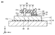
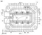
- FIG. FIG. 5 is a schematic cross-sectional view taken along the cross-sectional line II-II shown in FIG. 1 of the power semiconductor module of the first embodiment.
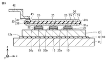
- FIG. 3 is a schematic cross-sectional view taken along the cross-sectional line III-III shown in FIG. 1 of the power semiconductor module of the first embodiment.
- FIG. 5 is a schematic cross-sectional view taken along the cross-sectional line IV-IV shown in FIG. 1 of the power semiconductor module of the first embodiment.
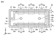
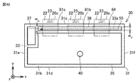
- It is a schematic partial enlarged plan view of the printed wiring board included in the power semiconductor module of Embodiment 1.
- FIG. It is a schematic partial enlarged plan view of the printed wiring board included in the power semiconductor module of Embodiment 1.
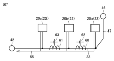
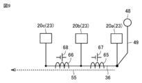
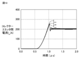
- FIG. It is an equivalent circuit diagram from the emitter control terminal to the 1st electrode terminal of the power semiconductor module of Embodiment 1 and the comparative example. It is a figure which shows the time waveform of the collector-emitter current which flows in the power semiconductor element when the power semiconductor element is turned on in the power semiconductor module of the comparative example. It is an equivalent circuit diagram from the gate control terminal to the gate electrode of the power semiconductor element of the power semiconductor module of Embodiment 1. FIG. It is a figure which shows the time waveform of the collector-emitter current which flows in the power semiconductor element when the power semiconductor element is turned on in the power semiconductor module of Embodiment 1. FIG.
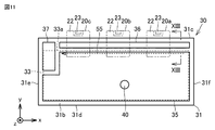
- FIG. 11 is a schematic partially enlarged cross-sectional view taken along the cross-sectional line XIII-XIII shown in FIG. 11 of the power semiconductor module of the first modification of the first embodiment.
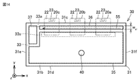
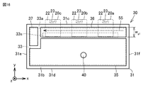
- FIG. 11 is a schematic partial enlarged plan view of the printed wiring board included in the power semiconductor module of the 2nd modification of Embodiment 1.
- FIG. It is a schematic partial enlarged plan view of the printed wiring board included in the power semiconductor module of the 2nd modification of Embodiment 1.
- FIG. 5 is a schematic cross-sectional view taken along the cross-sectional line XXI-XXI shown in FIG.
- FIG. 5 is a schematic cross-sectional view taken along the cross-sectional line XXII-XXII shown in FIG. 20 of the power semiconductor module of the second embodiment.
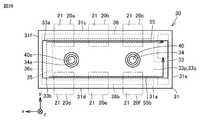
- It is a schematic partial enlarged plan view of the printed wiring board included in the power semiconductor module of Embodiment 2.
- FIG. 2 It is a schematic partial enlarged plan view of the printed wiring board included in the power semiconductor module of Embodiment 2.
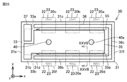
- FIG. 2 It is a schematic partial enlarged plan view of the printed wiring board included in the power semiconductor module of the 1st modification of Embodiment 2.
- FIG. It is a schematic partial enlarged plan view of the printed wiring board included in the power semiconductor module of the 1st modification of Embodiment 2.
- FIG. 5 is a schematic partially enlarged cross-sectional view taken along the cross-sectional line XXVII-XXVII shown in FIG. 25 of the power semiconductor module of the first modification of the second embodiment. It is a schematic partial enlarged plan view of the printed wiring board included in the power semiconductor module of the 2nd modification of Embodiment 2.
- FIG. It is a schematic partial enlarged plan view of the printed wiring board included in the power semiconductor module of the 2nd modification of Embodiment 2.
- FIG. It is a schematic partial enlarged plan view of the printed wiring board included in the power semiconductor module of the 3rd modification of Embodiment 2.
- FIG. It is a schematic partial enlarged plan view of the printed wiring board included in the power semiconductor module of the 3rd modification of Embodiment 2.
- FIG. 5 is a schematic partially enlarged cross-sectional view taken along the cross-sectional line XXVII-XXVII shown in FIG. 25 of the power semiconductor module of the first modification of the second embodiment.
- FIG. It is
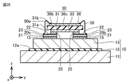
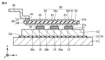
- FIG. 3 is a schematic cross-sectional view of the power semiconductor module of the third embodiment in the cross-sectional line XXXV-XXXV shown in FIG. 34.
- FIG. 3 is a schematic cross-sectional view of the power semiconductor module of the third embodiment in the cross-sectional line XXXVI-XXXVI shown in FIG. 34.
- FIG. 3 is a schematic cross-sectional view taken along the cross-sectional line XL-XL shown in FIG. 39 of the power semiconductor module of the fourth embodiment.
- FIG. 3 is a schematic cross-sectional view taken along the cross-sectional line XLI-XLI shown in FIG. 39 of the power semiconductor module of the fourth embodiment.
- FIG. 3 is a schematic cross-sectional view taken along the cross-sectional line XLII-XLII shown in FIG.
- FIG. 39 of the power semiconductor module of the fourth embodiment It is a schematic partial enlarged plan view of the printed wiring board included in the power semiconductor module of Embodiment 4.
- FIG. It is a schematic partial enlarged plan view of the printed wiring board included in the power semiconductor module of Embodiment 4.
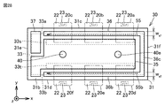
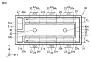
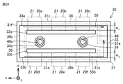
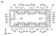
- FIG. It is a schematic plan view of the power semiconductor module of Embodiment 5.
- FIG. 5 is a schematic cross-sectional view of the power semiconductor module of the fifth embodiment in the cross-sectional line XLVI-XLVI shown in FIG. 45.
- FIG. 5 is a schematic cross-sectional view of the power semiconductor module of the fifth embodiment in the cross-sectional line XLVII-XLVII shown in FIG. 45.
- FIG. 5 is a schematic cross-sectional view taken along the cross-sectional line LL shown in FIG. 49 of the power semiconductor module of the first modification of the fifth embodiment.
- FIG. 5 is a schematic partial enlarged plan view of the printed wiring board included in the power semiconductor module of the 1st modification of Embodiment 5.
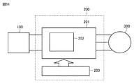
- It is the schematic sectional drawing of the power semiconductor module of the 2nd modification of Embodiment 5. It is a block diagram which shows the structure of the power conversion system which concerns on Embodiment 6.
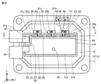
- the power semiconductor module 1 of the first embodiment will be described with reference to FIGS. 1 to 6.
- the power semiconductor module 1 mainly includes an insulating circuit board 10, power semiconductor elements 20a, 20b, 20c, a printed wiring board 30, and a conductive wire 50.
- the power semiconductor module 1 may further include a conductive post 40, a first electrode terminal 42, a second electrode terminal 44, an emitter control terminal 46, and a gate control terminal 48.
- the insulating circuit board 10 includes an insulating plate 12 and a conductive circuit pattern 13.
- the insulating circuit board 10 may further include a base plate 11.
- the insulating plate 12 includes the main surface 12a.
- the main surface 12a of the insulating plate 12 extends in the first direction (x direction) and the second direction (y direction).
- the insulating plate 12 is not particularly limited, but is an inorganic ceramic such as alumina (Al 2 O 3 ), aluminum nitride (AlN), silicon nitride (Si 3 N 4 ), silicon dioxide (SiO 2 ) or boron nitride (BN). It may be formed of a material.
- the insulating plate 12 may be formed of a resin material in which at least one of fine particles and a filler is dispersed.
- At least one of fine particles and filler for example, alumina (Al 2 O 3), aluminum nitride (AlN), silicon nitride (Si 3 N 4), silicon dioxide (SiO 2), boron nitride (BN), diamond (C ), Silicon carbide (SiC) or boron oxide (B 2 O 3 ) may be formed of an inorganic ceramic material, or may be formed of a resin material such as a silicone resin or an acrylic resin.
- the resin in which at least one of the fine particles and the filler is dispersed is not particularly limited, but may be formed of an epoxy resin, a polyimide resin, a silicone resin, or an acrylic resin.
- the conductive circuit pattern 13 is provided on the main surface 12a of the insulating plate 12.
- the conductive circuit pattern 13 is made of a metal such as copper or aluminum.
- the base plate 11 is provided on the main surface of the insulating plate 12 on the side opposite to the main surface 12a of the insulating plate 12.
- the base plate 11 is made of a metal such as copper or aluminum.
- the power semiconductor elements 20a, 20b, and 20c are power semiconductor elements such as an insulated gate bipolar transistor (IGBT) or a metal oxide semiconductor field effect transistor (MOSFET), respectively.
- the power semiconductor elements 20a, 20b, and 20c each include a collector electrode 21, an emitter electrode 22, and a gate electrode 23, respectively.
- the power semiconductor devices 20a, 20b, and 20c are mainly formed of silicon (Si) or a wide bandgap semiconductor material such as silicon carbide (SiC), gallium nitride (GaN), or diamond, respectively.
- the power semiconductor elements 20a, 20b, and 20c are fixed to the conductive circuit pattern 13. Specifically, the collector electrodes 21 of the power semiconductor devices 20a, 20b, and 20c are bonded to the conductive circuit pattern 13 by using a conductive bonding member 15 such as a solder, a metal fine particle sintered body, or a conductive adhesive. There is.
- the power semiconductor elements 20a, 20b, and 20c are electrically connected to the first emitter conductive pattern 33.
- the emitter electrodes 22 of the power semiconductor devices 20a, 20b, and 20c are bonded to the first emitter conductive pattern 33 by using a conductive bonding member 25 such as a solder, a metal fine particle sintered body, or a conductive adhesive. Has been done.
- the solder of the present specification is, for example, Sn-Ag-In-based solder, Sn-Ag-Cu-based solder, or the like.
- the metal fine particle sintered body of the present specification is, for example, a silver nanoparticle sintered body.
- the gate electrodes 23 of the power semiconductor elements 20a, 20b, 20c are electrically connected to the first gate conductive pattern 36.
- the power semiconductor elements 20a, 20b, and 20c are electrically connected in parallel to each other.
- the printed wiring board 30 is separated from the insulating circuit board 10 in the third direction (z direction) perpendicular to the first direction (x direction) and the second direction (y direction), and is the main component of the insulating plate 12. It is arranged so as to face the surface 12a.
- the printed wiring board 30 includes an insulating substrate 31, a first emitter conductive pattern 33, a first gate conductive pattern 36, and a first collector conductive pattern 35.
- the printed wiring board 30 may further include a first conductive pad 34, a second conductive pad 37, and a first conductive via 38.
- the insulating substrate 31 is, for example, a glass epoxy base material or a glass composite base material.
- the glass epoxy base material is formed by, for example, thermosetting a glass woven fabric impregnated with an epoxy resin.
- the glass composite base material is formed by, for example, thermosetting a glass nonwoven fabric impregnated with an epoxy resin.
- the insulating substrate 31 includes a main surface 31a and a main surface 31b on the opposite side of the main surface 31a.
- the longitudinal direction of the insulating substrate 31 is the first direction (x direction)
- the lateral direction of the insulating substrate 31 is the second direction (y direction).
- the plan view of the main surface 31b of the insulating substrate 31 is the same as the plan view of the main surface 31a of the insulating substrate 31.
- the lateral direction (y direction) of the insulating substrate 31 is perpendicular to the longitudinal direction (x direction) of the insulating substrate 31.
- the main surface 31a and the main surface 31b extend in the first direction (x direction) and the second direction (y direction).
- the longitudinal direction of the main surface 31a and the longitudinal direction of the main surface 31b are each in the first direction (x direction).
- the lateral direction of the main surface 31a and the lateral direction of the main surface 31b are each a second direction (y direction).
- the main surface 31a of the insulating substrate 31 faces the conductive circuit pattern 13.
- the main surface 31a of the insulating substrate 31 faces the main surface 12a of the insulating plate 12.
- the insulating substrate 31 includes an edge 31c, an edge 31d opposite to the edge 31c, an edge 31e, and an edge 31f opposite to the edge 31e.
- the edge 31c of the insulating substrate 31 may extend along the longitudinal direction (first direction (x direction)) of the insulating substrate 31, and is the long side of the insulating substrate 31 in the plan view of the main surface 31b of the insulating substrate 31. It may be.
- the edge 31d of the insulating substrate 31 may extend along the longitudinal direction (first direction (x direction)) of the insulating substrate 31, and is the long side of the insulating substrate 31 in the plan view of the main surface 31b of the insulating substrate 31. It may be.
- the edge 31c and the edge 31d face each other in the lateral direction (second direction (y direction)) of the insulating substrate 31.
- the edge 31e of the insulating substrate 31 connects the edge 31c and the edge 31d.
- the edge 31e of the insulating substrate 31 may extend along the lateral direction (second direction (y direction)) of the insulating substrate 31, and is short of the insulating substrate 31 in a plan view of the main surface 31b of the insulating substrate 31. It may be a side.
- the edge 31f of the insulating substrate 31 connects the edge 31c and the edge 31d.
- the edge 31f of the insulating substrate 31 may extend along the lateral direction (second direction (y direction)) of the insulating substrate 31, and is short of the insulating substrate 31 in a plan view of the main surface 31b of the insulating substrate 31. It may be a side.
- the edge 31e and the edge 31f face each other in the longitudinal direction (first direction (x direction)) of the insulating substrate 31.
- the first emitter conductive pattern 33, the first gate conductive pattern 36, the first collector conductive pattern 35, the first conductive pad 34, and the second conductive pad 37 are formed of a metal such as copper or aluminum. There is.
- the first emitter conductive pattern 33 and the first conductive pad 34 are provided on the main surface 31a.
- the main surface 31a of the insulating substrate 31 provided with the first emitter conductive pattern 33 faces the conductive circuit pattern 13.
- the main surface 31a of the insulating substrate 31 provided with the first emitter conductive pattern 33 faces the main surface 12a of the insulating plate 12.
- the first emitter conductive pattern 33 and the first conductive pad 34 are separated from each other and electrically insulated from each other.
- the first gate conductive pattern 36, the first collector conductive pattern 35, and the second conductive pad 37 are provided on the main surface 31b.
- the first gate conductive pattern 36, the first collector conductive pattern 35, and the second conductive pad 37 are separated from each other and electrically insulated from each other.
- the printed wiring board 30 is, for example, a double-sided copper-clad laminate.
- the first emitter conductive pattern 33 extends in the first direction (x direction) and the second direction (y direction).
- the longitudinal direction of the first emitter conductive pattern 33 is the first direction (x direction), and the lateral direction of the first emitter conductive pattern 33 is the second direction (y direction).
- the first emitter conductive pattern 33 includes a first edge 33a extending along the longitudinal direction (first direction (x direction)) of the first emitter conductive pattern 33.
- the first edge 33a of the first emitter conductive pattern 33 is arranged along the edge 31c of the insulating substrate 31.
- the first edge 33a of the first emitter conductive pattern 33 extends in the longitudinal direction (first direction (x direction)) of the insulating substrate 31.
- the first emitter conductive pattern 33 is connected to the first conductive via 38.
- the first conductive via 38 penetrates the insulating substrate 31.
- the first conductive via 38 electrically connects the first emitter conductive pattern 33 and the second conductive pad 37.
- the first conductive via 38 is made of a metal such as copper or aluminum.
- the first collector conductive pattern 35 extends in the first direction (x direction) and the second direction (y direction).
- the longitudinal direction of the first collector conductive pattern 35 is the first direction (x direction), and the lateral direction of the first collector conductive pattern 35 is the second direction (y direction).
- the first collector conductive pattern 35 is connected to the conductive post 40.
- the conductive post 40 penetrates the printed wiring board 30.
- the conductive post 40 is electrically connected to the conductive circuit pattern 13 and the first collector conductive pattern 35.
- the conductive post 40 is made of a metal such as copper or aluminum.
- the conductive post 40 supports the printed wiring board 30. Specifically, the conductive post 40 is fixed to the conductive circuit pattern 13 by using a conductive joining member (not shown) such as solder.
- the conductive post 40 is fixed to the first collector conductive pattern 35 and the first conductive pad 34 by using a conductive joining member (not shown) such as solder.
- the longitudinal direction of the first gate conductive pattern 36 is the first direction (x direction), and the lateral direction of the first gate conductive pattern 36 is the second direction (y direction).
- the longitudinal direction of the first gate conductive pattern 36 is the first direction (x direction) in which the edge 31c of the insulating substrate 31 extends.
- the longitudinal direction of the first gate conductive pattern 36 is the first direction (x direction) in which the first edge 33a of the first emitter conductive pattern 33 extends.
- the first gate conductive pattern 36 is arranged along the edge 31c of the insulating substrate 31 in the plan view of the main surface 31b of the insulating substrate 31.
- the first gate conductive pattern 36 is arranged along the first edge 33a of the first emitter conductive pattern 33 in a plan view of the main surface 31b of the insulating substrate 31.
- the first gate conductive pattern 36 overlaps with the first edge 33a of the first emitter conductive pattern 33.
- the center line of the first gate conductive pattern 36 in the lateral direction (second direction (y direction)) of the first gate conductive pattern 36 is the first. 1 It overlaps with the first edge 33a of the emitter conductive pattern 33.
- the first width w g1 of the first gate conductive pattern 36 is the longitudinal direction (first direction (x direction)) of the first gate conductive pattern 36 in the plan view of the main surface 31b of the insulating substrate 31 among the first emitter conductive patterns 33. )) Is smaller than the width w e1 of the first portion 33p corresponding to the first gate conductive pattern 36.
- the first width w g1 of the first gate conductive pattern 36 may be less than half the width w e1 of the first portion 33p of the first emitter conductive pattern 33, and the first portion of the first emitter conductive pattern 33.
- the width w e1 of 33p may also be one-third or less of the width w e1 of 33p, may also be a quarter or less of the width w e1 of the first portion 33p of the first emitter conductive pattern 33, the first emitter conductive pattern 33 It may be less than one-fifth of the width w e1 of the first portion 33p of the above.
- the first width w g1 of the first gate conductive pattern 36 is defined as the length of the first gate conductive pattern 36 in the lateral direction (second direction (y direction)) of the first gate conductive pattern 36.
- the width w e1 of the first portion 33p of the first emitter conductive pattern 33 is the length of the first portion 33p of the first emitter conductive pattern 33 in the lateral direction (second direction (y direction)) of the first emitter conductive pattern 33. Defined as a conductor.
- the inductance of the conductive pattern increases.
- the first width w g1 of the first gate conductive pattern 36 is narrower than the width w e1 of the first portion 33p of the first emitter conductive pattern 33. Therefore, the parasitic inductances 65 and 66 (see FIG. 9) of the first gate conductive pattern 36 can be made larger than the parasitic inductances 60 and 61 (see FIG. 7) of the first emitter conductive pattern 33.
- the conductive wire 47 is bonded to the emitter electrode 22 of the power semiconductor element 20a and the emitter control terminal 46.
- the power semiconductor element 20a to which the conductive wire 47 is connected is a power semiconductor element most distal to the first electrode terminal 42 or the edge 31e of the insulating substrate 31 among the power semiconductor elements 20a, 20b, 20c.
- the power semiconductor element 20a to which the conductive wire 47 is connected is a power semiconductor element most proximal to the edge 31f of the insulating substrate 31 among the power semiconductor elements 20a, 20b, 20c.
- the conductive wire 47 is made of a metal such as gold, silver, copper or aluminum.
- the emitter control terminal 46 is provided on, for example, an insulating block (not shown) placed on the base plate 11. An emitter voltage is supplied to the emitter control terminal 46 from the outside of the power semiconductor module 1.
- the emitter control terminal 46 is made of a metal such as copper or aluminum.
- the emitter control terminal 46 is connected to the emitter electrode 22 of the power semiconductor element 20a via a conductive wire 47.
- the emitter control terminal 46 is connected to the emitter electrodes 22 of the power semiconductor devices 20b and 20c via the conductive wire 47, the emitter electrode 22 of the power semiconductor element 20a, and the first emitter conductive pattern 33.
- the power semiconductor elements 20a, 20b, and 20c are arranged along the first edge 33a of the first emitter conductive pattern 33.
- the power semiconductor elements 20a, 20b, and 20c are arranged along the first gate conductive pattern 36.
- the power semiconductor elements 20a, 20b, and 20c are arranged along the edge 31c of the insulating substrate 31.
- the longitudinal direction (first direction (x direction)) of the first gate conductive pattern 36 is the arrangement direction of the power semiconductor elements 20a, 20b, 20c (first direction (x direction)). )).
- the arrangement direction (first direction (x direction)) of the power semiconductor elements 20a, 20b, 20c is the longitudinal direction (first direction (x direction)) of the insulating substrate 31. be.
- the gate electrodes 23 of the power semiconductor elements 20a, 20b, 20c are exposed from the insulating substrate 31 (printed wiring board 30).
- the conductive wire 50 is bonded to the gate electrode 23 of the power semiconductor elements 20a, 20b, 20c and the first gate conductive pattern 36.
- the conductive wire 50 is made of a metal such as gold, silver, copper or aluminum.
- the gate electrodes 23 of the power semiconductor elements 20a, 20b, and 20c are electrically connected to the first gate conductive pattern 36 via the conductive wire 50.
- the conductive wire 49 is bonded to the first gate conductive pattern 36 and the gate control terminal 48.
- the conductive wire 49 is made of a metal such as gold, silver, copper or aluminum.
- the first gate conductive pattern 36 is electrically connected to the gate control terminal 48 via the conductive wire 49.
- a gate voltage is supplied to the gate control terminal 48 from the outside of the power semiconductor module 1.
- the gate control terminal 48 is provided, for example, on an insulating block (not shown) placed on the base plate 11.
- the gate control terminal 48 is made of a metal such as copper or aluminum.
- the gate control terminal 48 is electrically connected to the gate electrodes 23 of the power semiconductor elements 20a, 20b, 20c via the conductive wire 49, the first gate conductive pattern 36, and the conductive wire 50.
- An emitter-gate voltage is supplied between the emitter control terminal 46 and the gate control terminal 48 from the outside of the power semiconductor module 1. Depending on the emitter-gate voltage, the power semiconductor devices 20a, 20b, 20c are switched between the on state and the off state.
- the first electrode terminal 42 and the second electrode terminal 44 are made of a metal such as copper or aluminum, for example. In a plan view of the main surface 31b of the insulating substrate 31, the first electrode terminal 42 and the second electrode terminal 44 are arranged on the edge 31e of the insulating substrate 31.
- the first electrode terminal 42 is fixed to the second conductive pad 37 by using a conductive joining member 43 such as solder. As shown in FIG. 3, the first electrode terminal 42 is connected to the power semiconductor elements 20a, 20b, 20c via the second conductive pad 37, the first conductive via 38, the first emitter conductive pattern 33, and the conductive bonding member 25. It is electrically connected to the emitter electrode 22 of the above.
- the first electrode terminal 42 functions as an emitter electrode terminal.
- the second electrode terminal 44 is fixed to the first collector conductive pattern 35 by using a conductive joining member 45 such as solder. As shown in FIGS. 3 and 4, the second electrode terminal 44 has the power semiconductor elements 20a, 20b, 20c via the first collector conductive pattern 35, the conductive post 40, the conductive circuit pattern 13, and the conductive joining member 15. It is electrically connected to the collector electrode 21 of the above.
- the second electrode terminal 44 functions as a collector electrode terminal.
- a part of the conductive circuit pattern 13 functions as a collector conductive pattern. That is, the conductive circuit pattern 13 includes a collector conductive pattern.
- the operation of the power semiconductor module 1 of the present embodiment will be described with reference to FIGS. 5 to 10 in comparison with the power semiconductor module of the comparative example.
- the first gate conductive pattern 36 is the first edge of the first emitter conductive pattern 33 in the plan view of the main surface 31b of the insulating substrate 31. Not arranged along 33a.
- the gate-emitter voltage applied to each of the power semiconductor devices 20a, 20b, 20c (that is, the difference between the gate voltage applied to the gate control terminal 48 and the emitter voltage applied to the emitter control terminal 46).
- the power semiconductor elements 20a, 20b, and 20c are turned on by making the voltage larger than the threshold voltage.
- the main current 55 is from the second electrode terminal 44 to the first collector conductive pattern 35, the conductive post 40, the conductive circuit pattern 13, the power semiconductor elements 20a, 20b, 20c, the first emitter conductive pattern 33, the first conductive via 38, and the like. It flows through the second conductive pad 37 to the first electrode terminal 42.
- the main current 55 flows in the order of the power semiconductor element 20a, the power semiconductor element 20b, and the power semiconductor element 20c.
- the edge of the conductive pattern is the part of the conductive pattern where the most current flows. Therefore, as shown in FIGS. 5 and 6, the main current 55 flows along the first edge 33a proximal to the power semiconductor elements 20a, 20b, 20c of the first emitter conductive pattern 33.
- the main current 55 flowing through the first emitter conductive pattern 33 forms a magnetic flux ⁇ around the main current 55 (for example, in the first emitter conductive pattern 33).
- the main current 55 increases with time (see FIG. 8 or 10), and the magnetic flux ⁇ formed by the main current 55 also increases with time.
- the first emitter conductive pattern 33 has parasitic inductances 60 and 61. Therefore, the time change d ⁇ / dt of the magnetic flux ⁇ formed by the main current 55 flowing along the first edge 33a of the first emitter conductive pattern 33 is the first induced electromotive force 62, 63 (1st induced electromotive force 62, 63) in the first emitter conductive pattern 33. (See FIG. 7).
- the first induced electromotive force 62, 63 fluctuates the emitter voltage among the power semiconductor elements 20a, 20b, 20c.
- the first induced electromotive forces 62 and 63 are the first gate-emitter voltage V gea of the power semiconductor element 20a, the second gate-emitter voltage V geb of the power semiconductor element 20b, and the third gate of the power semiconductor element 20c.
- the voltage between emitters V gec and the voltage V gec are made different from each other.
- the collector-emitter current of one of the power semiconductor devices 20a, 20b, and 20c of the power semiconductor device 20c rapidly increases.
- the collector-emitter current of the power semiconductor device 20c is higher than that of the collector-emitter current I cea of the power semiconductor device 20a and the collector-emitter current I ceb of the power semiconductor device 20b. I cec surges.
- the collector-emitter current Icec of the power semiconductor element 20c exceeds the rated current of the power semiconductor element 20c, and the power semiconductor element 20c is destroyed.
- the life of the power semiconductor module of the comparative example is relatively short.
- the first gate conductive pattern 36 is arranged along the first edge 33a of the first emitter conductive pattern 33 in the plan view of the main surface 31b of the insulating substrate 31. Has been done. Therefore, the main current 55 flowing through the first emitter conductive pattern 33 also forms a magnetic flux ⁇ in the first gate conductive pattern 36.
- the first gate conductive pattern 36 has parasitic inductances 65 and 66.
- the time variation d ⁇ / dt of the magnetic flux ⁇ formed by the main current 55 flowing along the first edge 33a of the first emitter conductive pattern 33 is the second induced electromotive force 67,68 (FIG. 9) in the first gate conductive pattern 36. See).
- the second induced electromotive force 67, 68 fluctuates the gate voltage between the power semiconductor elements 20a, 20b, 20c.
- the fluctuation of the gate voltage between the power semiconductor elements 20a, 20b and 20c cancels at least a part of the fluctuation of the emitter voltage between the power semiconductor elements 20a, 20b and 20c.
- the fluctuation of the gate voltage between the power semiconductor elements 20a, 20b and 20c completely cancels the fluctuation of the emitter voltage between the power semiconductor elements 20a, 20b and 20c.
- the difference between the second gate-emitter voltage V gea of the power semiconductor device 20b and the first gate-emitter voltage V gea of the power semiconductor device 20a is reduced.
- the difference between the third gate-emitter voltage V gec of the power semiconductor element 20c and the second gate-emitter voltage V geb of the power semiconductor element 20b is reduced.
- the first gate-emitter voltage V gea of the power semiconductor device 20a, the second gate-emitter voltage V geb of the power semiconductor device 20b, and the third gate-emitter voltage V gec of the power semiconductor device 20c. are equal to each other.
- the parasitic inductances 65 and 66 of the first gate conductive pattern 36 are made larger than the parasitic inductances 60 and 61 of the first emitter conductive pattern 33.
- the parasitism of the first gate conductive pattern 36 The inductances 65 and 66 can be made larger than the parasitic inductances 60 and 61 of the first emitter conductive pattern 33.
- the fluctuation of the gate voltage between the power semiconductor elements 20a, 20b and 20c can further cancel the fluctuation of the emitter voltage between the power semiconductor elements 20a, 20b and 20c. Fluctuations between the first gate-emitter voltage V gea of the power semiconductor device 20a, the second gate-emitter voltage V geb of the power semiconductor device 20b, and the third gate-emitter voltage V gec of the power semiconductor device 20c. It can be made even smaller.
- the first gate conductive pattern 36 is the first emitter conductive pattern 33. It may be separated from one edge 33a.
- the distance d 1 is 3.0 mm or less. Therefore, the fluctuation of the gate voltage between the power semiconductor elements 20a, 20b, and 20c increases. The fluctuation of the gate voltage between the power semiconductor elements 20a, 20b and 20c can further cancel the fluctuation of the emitter voltage between the power semiconductor elements 20a, 20b and 20c. The collector-emitter current of the power semiconductor elements 20a, 20b, and 20c is prevented from suddenly increasing. The life of the power semiconductor module 1 can be extended.
- the first center line and the first emitter conductive pattern 33 in the lateral direction (second direction (y direction)) of the first gate conductive pattern 36 The second maximum distance d 2 between them is 7 times or less the thickness T of the insulating substrate 31. Therefore, the fluctuation of the gate voltage between the power semiconductor elements 20a, 20b, and 20c increases. The fluctuation of the gate voltage between the power semiconductor elements 20a, 20b and 20c can further cancel the fluctuation of the emitter voltage between the power semiconductor elements 20a, 20b and 20c. The collector-emitter current of the power semiconductor elements 20a, 20b, and 20c is prevented from suddenly increasing. The life of the power semiconductor module 1 can be extended.
- the third maximum distance d 3 between the first gate conductive pattern 36 and the first emitter conductive pattern 33 is the thickness T of the insulating substrate 31. It is less than 5 times. Therefore, the fluctuation of the gate voltage between the power semiconductor elements 20a, 20b, and 20c increases. The fluctuation of the gate voltage between the power semiconductor elements 20a, 20b and 20c can further cancel the fluctuation of the emitter voltage between the power semiconductor elements 20a, 20b and 20c. The collector-emitter current of the power semiconductor elements 20a, 20b, and 20c is prevented from suddenly increasing. The life of the power semiconductor module 1 can be extended.
- the first emitter conductive pattern 33 is provided with the first slit 33s along the first edge 33a of the first emitter conductive pattern 33. ing.
- the outer edge of the first slit 33s is also the edge of the first emitter conductive pattern 33.
- the main current 55 flowing through the first emitter conductive pattern 33 is applied to the first region of the first emitter conductive pattern 33 between the first edge 33a and the first slit 33s of the first emitter conductive pattern 33. It flows intensively.
- the magnetic flux ⁇ formed by the main current 55 in the first gate conductive pattern 36 increases.
- the magnitude of the time change d ⁇ / dt of the magnetic flux ⁇ in the first gate conductive pattern 36 increases.
- the magnitude of the second induced electromotive force 67,68 (see FIG. 9) generated in the first gate conductive pattern 36 increases. Fluctuations in the gate voltage between the power semiconductor devices 20a, 20b, and 20c increase. The fluctuation of the gate voltage between the power semiconductor elements 20a, 20b and 20c can further cancel the fluctuation of the emitter voltage between the power semiconductor elements 20a, 20b and 20c. The collector-emitter current of the power semiconductor elements 20a, 20b, and 20c is prevented from suddenly increasing. The life of the power semiconductor module 1 can be extended.
- the first width w g1 of the first gate conductive pattern 36 is the first edge 33a and the first slit 33s of the first emitter conductive pattern 33 among the first emitter conductive patterns 33. It may be narrower than the second width w r1 of the first region between and.
- the second width w r1 of the first region of the first emitter conductive pattern 33 is the length of the first region of the first emitter conductive pattern 33 in the lateral direction (second direction (y direction)) of the first gate conductive pattern 36. Defined as a conductor.
- the first width w g1 of the first gate conductive pattern 36 is the first emitter conductive pattern among the first emitter conductive patterns 33. It is wider than the second width w r1 of the first region between the first edge 33a of 33 and the first slit 33s.
- the magnetic flux ⁇ formed by the main current 55 in the first gate conductive pattern 36 increases.
- the magnitude of the second induced electromotive force 67, 68 (see FIG. 9) generated in the first gate conductive pattern 36 increases. Fluctuations in the gate voltage between the power semiconductor devices 20a, 20b, and 20c increase.
- the fluctuation of the gate voltage between the power semiconductor elements 20a, 20b and 20c can further cancel the fluctuation of the emitter voltage between the power semiconductor elements 20a, 20b and 20c.
- the collector-emitter current of the power semiconductor elements 20a, 20b, and 20c is prevented from suddenly increasing. The life of the power semiconductor module 1 can be extended.
- a portion 33h is provided.
- at least one of the power semiconductor elements 20a, 20b, 20c corresponding to at least one first retracting portion 33h is the first emitter in at least one first retracting portion 33h. It may be exposed from the conductive pattern 33.
- At least one first retracting portion 33h increases the distance between the main current 55b flowing through the first emitter conductive pattern 33 and the first gate conductive pattern 36. At least one first retracting portion 33h reduces the magnetic flux ⁇ formed by the main current 55 in the first gate conductive pattern 36. At least one first retracting portion 33h reduces the magnitude of the second induced electromotive force 67,68 (see FIG. 9) generated in the first gate conductive pattern 36, and is between the power semiconductor elements 20a, 20b, and 20c. Reduces fluctuations in the gate voltage of. The at least one first retracting portion 33h prevents the fluctuation of the gate voltage between the power semiconductor elements 20a, 20b and 20c from excessively canceling the fluctuation of the emitter voltage between the power semiconductor elements 20a, 20b and 20c.
- At least one first retracting portion 33h may be a plurality of first retracting portions 33h.
- the plurality of first retracting portions 33h are provided on the first edge 33a of the first emitter conductive pattern 33 so as to correspond to the power semiconductor elements 20a, 20b, and 20c, respectively.
- the power semiconductor elements 20a, 20b, 20c may be exposed from the first emitter conductive pattern 33 in the plurality of first retracting portions 33h.
- the plurality of first retreating portions 33h prevent the fluctuation of the gate voltage between the power semiconductor elements 20a, 20b and 20c from excessively canceling the fluctuation of the emitter voltage between the power semiconductor elements 20a, 20b and 20c.
- the power semiconductor module 1 of the present embodiment includes an insulating circuit substrate 10, a first power semiconductor element (for example, a power semiconductor element 20a), a second power semiconductor element (for example, a power semiconductor element 20c), and a printed wiring substrate. 30 and are provided.
- the insulating circuit board 10 includes an insulating plate 12 including a first main surface (main surface 12a) and a conductive circuit pattern 13 provided on the first main surface of the insulating plate 12.
- the first power semiconductor element includes a first emitter electrode (for example, the emitter electrode 22 of the power semiconductor element 20a) and a first gate electrode (for example, the gate electrode 23 of the power semiconductor element 20a).
- the second power semiconductor element includes a second emitter electrode (for example, the emitter electrode 22 of the power semiconductor element 20c) and a second gate electrode (for example, the gate electrode 23 of the power semiconductor element 20c).
- the printed wiring board 30 is arranged so as to face the first main surface of the insulating plate 12.
- the printed wiring board 30 includes an insulating substrate 31, a first emitter conductive pattern 33, and a first gate conductive pattern 36.
- the insulating substrate 31 includes a second main surface (for example, the main surface 31a) and a third main surface (for example, the main surface 31b) opposite to the second main surface.
- the first power semiconductor element and the second power semiconductor element are fixed to the conductive circuit pattern 13.
- the first emitter electrode (for example, the emitter electrode 22 of the power semiconductor element 20a) and the second emitter electrode (for example, the emitter electrode 22 of the power semiconductor element 20c) are electrically connected to the first emitter conductive pattern 33.
- the first gate electrode (for example, the gate electrode 23 of the power semiconductor element 20a) and the second gate electrode (for example, the gate electrode 23 of the power semiconductor element 20c) are electrically connected to the first gate conductive pattern 36.
- the first emitter conductive pattern 33 is provided on the second main surface (for example, the main surface 31a).
- the first gate conductive pattern 36 is provided on the third main surface (for example, the main surface 31b), and is the first emitter in a plan view of the third main surface (for example, the main surface 31b) of the insulating substrate 31. It is arranged along the first edge 33a of the conductive pattern 33.
- the power semiconductor module 1 includes a second power semiconductor element (for example, a power semiconductor element 20c) in addition to a first power semiconductor element (for example, a power semiconductor element 20a). Therefore, the power capacity of the power semiconductor module 1 can be increased.
- a second power semiconductor element for example, a power semiconductor element 20c
- a first power semiconductor element for example, a power semiconductor element 20a
- the first gate conductive pattern 36 is arranged along the first edge 33a of the first emitter conductive pattern 33 in a plan view of the third main surface (for example, the main surface 31b) of the insulating substrate 31. Therefore, the main current 55 flowing through the first emitter conductive pattern 33 forms a magnetic flux ⁇ not only in the first emitter conductive pattern 33 but also in the first gate conductive pattern 36.
- the time change d ⁇ / dt of the magnetic flux ⁇ at the time of turn-on of the first power semiconductor element (for example, the power semiconductor element 20a) and the second power semiconductor element (for example, the power semiconductor element 20c) is first in the first emitter conductive pattern 33. Induced electromotive forces 62,63 (see FIG. 7) are generated, and second induced electromotive forces 67,68 (see FIG. 9) are generated in the first gate conductive pattern 36.
- the first induced electromotive force 62, 63 generated in the first emitter conductive pattern 33 is between a first power semiconductor element (for example, a power semiconductor element 20a) and a second power semiconductor element (for example, a power semiconductor element 20c). It causes fluctuations in the emitter voltage.
- the second induced electromotive force 67,68 (see FIG. 9) generated in the first gate conductive pattern 36 causes a variation in the gate voltage between the first power semiconductor element and the second power semiconductor element. At least a part of the fluctuation of the emitter voltage between the first power semiconductor element (for example, the power semiconductor element 20a) and the second power semiconductor element (for example, the power semiconductor element 20c) is the first power semiconductor element and the second power. It is canceled by the fluctuation of the gate voltage between the semiconductor element and the device.
- the collector-emitter current of the first power semiconductor element and the second power semiconductor element is prevented from rapidly increasing. The life of the power semiconductor module 1 can be extended.
- the first gate conductive pattern 36 and the first emitter conductive pattern 33 in the cross section perpendicular to the first longitudinal direction (first direction (x direction)) of the first gate conductive pattern 36.
- the first maximum distance d 1 between and is 3.0 mm or less.
- the first power semiconductor element for example, the power semiconductor element 20a
- This fluctuation in the gate voltage can further cancel the fluctuation in the emitter voltage between the first power semiconductor element and the second power semiconductor element.
- the collector-emitter current of the first power semiconductor element and the second power semiconductor element is prevented from rapidly increasing. The life of the power semiconductor module 1 can be extended.
- the first lateral direction (first direction (x direction)) of the first gate conductive pattern 36 is 7 times or less the thickness T of the insulating substrate 31.
- the first power semiconductor element for example, the power semiconductor element 20a
- the second power semiconductor element for example, the power semiconductor element 20c
- the third gate conductive pattern 36 and the first emitter conductive pattern 33 are located in the plan view of the third main surface (for example, the main surface 31b) of the insulating substrate 31.
- the maximum distance d 3 is 5 times or less the thickness T of the insulating substrate 31.
- the third maximum distance d 3 is 5 times or less the thickness T of the insulating substrate 31, the first power semiconductor element (for example, the power semiconductor element 20a) and the second power semiconductor element (for example, the power semiconductor element 20c)
- the fluctuation of the gate voltage between increases.
- This fluctuation in the gate voltage can further cancel the fluctuation in the emitter voltage between the first power semiconductor element and the second power semiconductor element.
- the collector-emitter current of the first power semiconductor element and the second power semiconductor element is prevented from rapidly increasing. The life of the power semiconductor module 1 can be extended.
- the first gate conductive pattern 36 is the first edge 33a of the first emitter conductive pattern 33. It overlaps with.
- the magnetic flux ⁇ formed by the main current 55 flowing through the first emitter conductive pattern 33 in the first gate conductive pattern 36 increases.
- the fluctuation of the gate voltage between the first power semiconductor element (for example, the power semiconductor element 20a) and the second power semiconductor element (for example, the power semiconductor element 20c) increases.
- This fluctuation in the gate voltage can further cancel the fluctuation in the emitter voltage between the first power semiconductor element and the second power semiconductor element.
- the collector-emitter current of the first power semiconductor element and the second power semiconductor element is prevented from rapidly increasing. The life of the power semiconductor module 1 can be extended.
- the lateral direction (second direction (y direction)) of the first gate conductive pattern 36 in the plan view of the third main surface (for example, the main surface 31b) of the insulating substrate 31, the lateral direction (second direction (y direction)) of the first gate conductive pattern 36.
- the center line of the first gate conductive pattern 36 in the above overlaps with the first edge 33a of the first emitter conductive pattern 33.
- the magnetic flux ⁇ formed in the first gate conductive pattern 36 by the main current 55 flowing through the first emitter conductive pattern 33 further increases.
- the fluctuation of the gate voltage between the first power semiconductor element (for example, the power semiconductor element 20a) and the second power semiconductor element (for example, the power semiconductor element 20c) increases.
- This fluctuation in the gate voltage can further cancel the fluctuation in the emitter voltage between the first power semiconductor element and the second power semiconductor element.
- the collector-emitter current of the first power semiconductor element and the second power semiconductor element is prevented from rapidly increasing. The life of the power semiconductor module 1 can be extended.
- the first emitter conductive pattern 33 is provided with a first slit 33s along the first edge 33a of the first emitter conductive pattern 33.
- the main current 55 flowing through the first emitter conductive pattern 33 is concentrated in the first region of the first emitter conductive pattern 33 between the first edge 33a and the first slit 33s of the first emitter conductive pattern 33. It flows.
- the magnetic flux ⁇ formed by the main current 55 flowing through the first emitter conductive pattern 33 in the first gate conductive pattern 36 increases.
- the fluctuation of the gate voltage between the first power semiconductor element (for example, the power semiconductor element 20a) and the second power semiconductor element (for example, the power semiconductor element 20c) increases. This fluctuation in the gate voltage can further cancel the fluctuation in the emitter voltage between the first power semiconductor element and the second power semiconductor element.
- the collector-emitter current of the first power semiconductor element and the second power semiconductor element is prevented from rapidly increasing. The life of the power semiconductor module 1 can be extended.
- the first width w g1 of the first gate conductive pattern 36 is the first edge 33a and the first slit 33s of the first emitter conductive pattern 33 among the first emitter conductive patterns 33. It is wider than the second width w r1 of the first region between and.
- the magnetic flux ⁇ formed by the main current 55 flowing through the first emitter conductive pattern 33 in the first gate conductive pattern 36 increases.
- the fluctuation of the gate voltage between the first power semiconductor element (for example, the power semiconductor element 20a) and the second power semiconductor element (for example, the power semiconductor element 20c) increases.
- This fluctuation in the gate voltage can further cancel the fluctuation in the emitter voltage between the first power semiconductor element and the second power semiconductor element.
- the collector-emitter current of the first power semiconductor element and the second power semiconductor element is prevented from rapidly increasing. The life of the power semiconductor module 1 can be extended.
- At least one first retracting portion 33h recessed from the first edge 33a is provided on the first edge 33a of the first emitter conductive pattern 33.
- At least one first retracting portion 33h reduces the magnetic flux ⁇ formed in the first gate conductive pattern 36 by the main current 55 flowing through the first emitter conductive pattern 33.
- the fluctuation of the gate voltage between the first power semiconductor element (for example, the power semiconductor element 20a) and the second power semiconductor element (for example, the power semiconductor element 20c) is the first power. It prevents the fluctuation of the emitter voltage between the semiconductor element and the second power semiconductor element from being excessively canceled.
- the collector-emitter current of the first power semiconductor element and the second power semiconductor element is prevented from rapidly increasing. The life of the power semiconductor module 1 can be extended.
- At least one first retracting portion 33h is a plurality of first retracting portions 33h.
- the plurality of first retracting portions 33h of the first emitter conductive pattern 33 correspond to the first power semiconductor element (for example, the power semiconductor element 20a) and the second power semiconductor element (for example, the power semiconductor element 20c). It is provided on the first edge 33a.
- the plurality of first retracting portions 33h reduce the magnetic flux ⁇ formed in the first gate conductive pattern 36 by the main current 55 flowing through the first emitter conductive pattern 33.
- the fluctuation of the gate voltage between the first power semiconductor element (for example, the power semiconductor element 20a) and the second power semiconductor element (for example, the power semiconductor element 20c) causes the fluctuation of the gate voltage to be the first power semiconductor. It prevents the fluctuation of the emitter voltage between the element and the second power semiconductor element from being excessively canceled.
- the collector-emitter current of the first power semiconductor element and the second power semiconductor element is prevented from rapidly increasing. The life of the power semiconductor module 1 can be extended.
- the first edge 33a and the first gate conductive pattern 36 of the first emitter conductive pattern 33 are a first power semiconductor element (for example, a power semiconductor element 20a) and a second power semiconductor. It is arranged along an element (for example, a power semiconductor element 20c). Therefore, the electrical connection between the gate electrode 23 of the first power semiconductor element and the second power semiconductor element and the first gate conductive pattern 36 becomes easy. The electrical connection between the emitter electrode 22 of the first power semiconductor element and the second power semiconductor element and the first emitter conductive pattern 33 becomes easy.
- the second main surface (for example, the main surface 31a) of the insulating substrate 31 faces the conductive circuit pattern 13. Therefore, the power capacity of the power semiconductor module 1 can be increased, and the life of the power semiconductor module 1 can be extended.
- the first width w g1 of the first gate conductive pattern 36 is the third in the plan view of the third main surface (for example, the main surface 31b) of the first emitter conductive pattern 33. It is smaller than the width w e1 of the first portion 33p corresponding to the first gate conductive pattern 36 in the first longitudinal direction (x direction) of the one gate conductive pattern 36.
- the parasitic inductances 65 and 66 of the first gate conductive pattern 36 can be made larger than the parasitic inductances 60 and 61 of the first emitter conductive pattern 33.
- the fluctuation of the gate voltage between the first power semiconductor element (for example, the power semiconductor element 20a) and the second power semiconductor element (for example, the power semiconductor element 20c) increases.
- This fluctuation in the gate voltage can further cancel the fluctuation in the emitter voltage between the first power semiconductor element and the second power semiconductor element.
- the collector-emitter current of the first power semiconductor element and the second power semiconductor element is prevented from rapidly increasing.
- the life of the power semiconductor module 1 can be extended. Further, the adverse effect of noise generated during the switching operation of the first power semiconductor element and the second power semiconductor element on the first gate conductive pattern 36 can be reduced.
- Embodiment 2 The power semiconductor module 1e of the second embodiment will be described with reference to FIGS. 20 to 24.
- the power semiconductor module 1e of the present embodiment has the same configuration as the power semiconductor module 1 of the first embodiment, but is mainly different in the following points.
- the power semiconductor module 1e further includes power semiconductor elements 20d, 20e, 20f, a conductive post 40e, and a conductive wire 50e.
- the printed wiring board 30 further includes a second gate conductive pattern 36b and a first conductive pad 34e.
- the printed wiring board 30 may further include a third gate conductive pattern 36c.
- the power semiconductor elements 20d, 20e, and 20f are power semiconductor elements such as an insulated gate bipolar transistor (IGBT) or a metal oxide semiconductor field effect transistor (MOSFET), respectively.
- the power semiconductor elements 20d, 20e, and 20f each include an emitter electrode 22, a gate electrode 23, and a collector electrode 21, respectively.
- the power semiconductor devices 20d, 20e, and 20f are mainly formed of silicon (Si) or a wide bandgap semiconductor material such as silicon carbide (SiC), gallium nitride (GaN), or diamond, respectively.
- the power semiconductor elements 20d, 20e, and 20f are fixed to the conductive circuit pattern 13. Specifically, the collector electrodes 21 of the power semiconductor devices 20d, 20e, and 20f are bonded to the conductive circuit pattern 13 by using a conductive bonding member 15 such as a solder, a metal fine particle sintered body, or a conductive adhesive. There is.
- the emitter electrodes 22 of the power semiconductor elements 20d, 20e, and 20f are electrically connected to the first emitter conductive pattern 33. Specifically, the emitter electrodes 22 of the power semiconductor devices 20d, 20e, and 20f are bonded to the first emitter conductive pattern 33 by using a conductive bonding member 25 such as a solder, a metal fine particle sintered body, or a conductive adhesive.
- the gate electrodes 23 of the power semiconductor elements 20d, 20e, 20f are electrically connected to the first gate conductive pattern 36.
- the power semiconductor elements 20d, 20e, and 20f are electrically connected in parallel to each other.
- the power semiconductor elements 20a, 20b, 20c and the power semiconductor elements 20d, 20e, 20f are electrically connected in parallel to each other.
- the numbers of the power semiconductor elements 20a, 20b, 20c, 20d, 20e, 20f included in the power semiconductor module 1e of the present embodiment are the power semiconductor elements 20a, 20b, 20c included in the power semiconductor module 1 of the first embodiment. More than the number of.
- the power semiconductor module 1e of the present embodiment has a larger current capacity than the power semiconductor module 1 of the first embodiment. Therefore, the power semiconductor module 1e of the present embodiment includes more conductive posts 40 and 40e than the power semiconductor module 1 of the first embodiment. Specifically, the power semiconductor module 1e further includes a conductive post 40e in addition to the conductive post 40.
- the first conductive pad 34e is provided on the main surface 31a of the insulating substrate 31.
- the first conductive pad 34e is separated from the first emitter conductive pattern 33 and the first conductive pad 34, and is electrically insulated from the first emitter conductive pattern 33 and the first conductive pad 34.
- the first conductive pad 34e is made of a metal such as copper or aluminum.
- the first collector conductive pattern 35 is connected to the conductive post 40e.
- the conductive post 40e penetrates the printed wiring board 30.
- the conductive post 40e is electrically connected to the conductive circuit pattern 13 and the first collector conductive pattern 35.
- the conductive post 40e is made of a metal such as copper or aluminum.
- the conductive post 40e supports the printed wiring board 30. Specifically, the conductive post 40e is fixed to the conductive circuit pattern 13 by using a conductive joining member (not shown) such as solder.
- the conductive post 40e is fixed to the first collector conductive pattern 35 and the first conductive pad 34e by using a conductive joining member (not shown) such as solder.
- the first emitter conductive pattern 33 includes a second edge 33b extending along the longitudinal direction (first direction (x direction)) of the first emitter conductive pattern 33.
- the second edge 33b of the first emitter conductive pattern 33 is arranged along the edge 31d of the insulating substrate 31.
- the second edge 33b of the first emitter conductive pattern 33 extends in the longitudinal direction (first direction (x direction)) of the insulating substrate 31.
- the second edge 33b of the first emitter conductive pattern 33 faces the first edge 33a of the first emitter conductive pattern 33 in the lateral direction (second direction (y direction)) of the first emitter conductive pattern 33. ..
- the second gate conductive pattern 36b is provided on the main surface 31b.
- the second gate conductive pattern 36b is made of a metal such as copper or aluminum.
- the second gate conductive pattern 36b is separated from the first collector conductive pattern 35 and the second conductive pad 37, and is electrically insulated from the first collector conductive pattern 35 and the second conductive pad 37. ..
- the longitudinal direction of the second gate conductive pattern 36b is the first direction (x direction), and the lateral direction of the second gate conductive pattern 36b is the second direction (y direction).
- the longitudinal direction of the second gate conductive pattern 36b is the first direction (x direction) in which the edge 31d of the insulating substrate 31 extends.
- the longitudinal direction of the second gate conductive pattern 36b is the first direction (x direction) in which the second edge 33b of the first emitter conductive pattern 33 extends.
- the second gate conductive pattern 36b is arranged along the edge 31d of the insulating substrate 31.
- the second gate conductive pattern 36b is arranged along the second edge 33b of the first emitter conductive pattern 33 opposite to the first edge 33a in the plan view of the main surface 31b of the insulating substrate 31.
- the second gate conductive pattern 36b overlaps with the second edge 33b of the first emitter conductive pattern 33.
- the second center line of the second gate conductive pattern 36b in the lateral direction (second direction (y direction)) of the second gate conductive pattern 36b is , It overlaps with the second edge 33b of the first emitter conductive pattern 33.
- the third width w g2 of the second gate conductive pattern 36b is the longitudinal direction (first direction (x direction)) of the second gate conductive pattern 36b in the plan view of the main surface 31b of the insulating substrate 31 among the first emitter conductive patterns 33. )) Is smaller than the width w e2 of the second portion 33q corresponding to the second gate conductive pattern 36b.
- the third width w g2 of the second gate conductive pattern 36b may be less than half the width w e2 of the second portion 33q of the first emitter conductive pattern 33, and the second portion of the first emitter conductive pattern 33.
- the width of the second portion 33q of the above may be less than one-fifth of the width w e2.
- the third width w g2 of the second gate conductive pattern 36b is defined as the length of the second gate conductive pattern 36b in the lateral direction (second direction (y direction)) of the second gate conductive pattern 36b.
- the width w e2 of the second portion 33q of the first emitter conductive pattern 33 is the length of the second portion 33q of the first emitter conductive pattern 33 in the lateral direction (second direction (y direction)) of the first emitter conductive pattern 33. Defined as a conductor.
- the second portion 33q of the first emitter conductive pattern 33 is the same as the first portion 33p of the first emitter conductive pattern 33.
- the inductance of the conductive pattern increases.
- the third width w g2 of the second gate conductive pattern 36b is narrower than the width w e2 of the second portion 33q of the first emitter conductive pattern 33. Therefore, the parasitic inductance of the second gate conductive pattern 36b can be made larger than the parasitic inductance of the first emitter conductive pattern 33.
- the second gate conductive pattern 36b is electrically connected to the first gate conductive pattern 36.
- the third gate conductive pattern 36c connects the first gate conductive pattern 36 and the second gate conductive pattern 36b.
- the second gate conductive pattern 36b is electrically connected to the first gate conductive pattern 36 via the third gate conductive pattern 36c.
- the second gate conductive pattern 36b is electrically connected to the gate control terminal 48 via the conductive wire 49, the first gate conductive pattern 36, and the third gate conductive pattern 36c.
- the third gate conductive pattern 36c is separated from the first collector conductive pattern 35 and the second conductive pad 37, and is electrically insulated from the first collector conductive pattern 35 and the second conductive pad 37. ..
- the third gate conductive pattern 36c is made of a metal such as copper or aluminum. Specifically, the third gate conductive pattern 36c is arranged along the edge 31f of the insulating substrate 31.
- the third gate conductive pattern 36c is arranged along the edge of the first emitter conductive pattern 33. More specifically, in the plan view of the main surface 31b of the insulating substrate 31, the third gate conductive pattern 36c overlaps the edge of the first emitter conductive pattern 33. In a plan view of the main surface 31b of the insulating substrate 31, the first gate conductive pattern 36, the second gate conductive pattern 36b, and the third gate conductive pattern 36c face the three sides of the first collector conductive pattern 35.
- the third gate conductive pattern 36c connects the first end of the first gate conductive pattern 36 and the second end of the second gate conductive pattern 36b.
- the first end of the first gate conductive pattern 36 is the end of the first gate conductive pattern 36 proximal to the edge 31f of the insulating substrate 31.
- the first end of the first gate conductive pattern 36 is the end of the first gate conductive pattern 36 distal to the first electrode terminal 42 and the second electrode terminal 44.
- the first end of the first gate conductive pattern 36 is the end of the end of the first gate conductive pattern 36 proximal to the power semiconductor element 20a to which the conductive wire 47 extending from the emitter control terminal 46 is bonded.
- the second end of the second gate conductive pattern 36b is the end of the second gate conductive pattern 36b proximal to the edge 31f of the insulating substrate 31.
- the second end of the second gate conductive pattern 36b is the end of the second gate conductive pattern 36b distal to the first electrode terminal 42 and the second electrode terminal 44.
- the second end of the second gate conductive pattern 36b is the end of the first gate conductive pattern 36 proximal to the power semiconductor element 20a to which the conductive wire 47 extending from the emitter control terminal 46 is bonded.
- the emitter control terminal 46 is connected to the emitter electrodes 22 of the power semiconductor elements 20d, 20e, 20f via the conductive wire 47, the emitter electrode 22 of the power semiconductor element 20a, and the first emitter conductive pattern 33.
- the power semiconductor elements 20d, 20e, and 20f are arranged along the second edge 33b of the first emitter conductive pattern 33.
- the power semiconductor elements 20d, 20e, and 20f are arranged along the second gate conductive pattern 36b.
- the power semiconductor elements 20d, 20e, and 20f are arranged along the edge 31d of the insulating substrate.
- the longitudinal direction (first direction (x direction)) of the second gate conductive pattern 36b is the arrangement direction of the power semiconductor elements 20d, 20e, 20f (first direction (x direction)). )).
- the arrangement direction (first direction (x direction)) of the power semiconductor elements 20d, 20e, 20f is the longitudinal direction (first direction (x direction)) of the insulating substrate 31. be.
- the gate electrodes 23 of the power semiconductor elements 20d, 20e, 20f are exposed from the insulating substrate 31 (printed wiring board 30).
- the conductive wire 50e is bonded to the gate electrodes 23 of the power semiconductor elements 20d, 20e, 20f and the second gate conductive pattern 36b.
- the conductive wire 50e is made of a metal such as gold, silver, copper or aluminum.
- the gate electrodes 23 of the power semiconductor elements 20d, 20e, and 20f are electrically connected to the second gate conductive pattern 36b via the conductive wire 50e.
- the gate control terminal 48 is a gate electrode 23 of the power semiconductor elements 20d, 20e, 20f via the conductive wire 49, the first gate conductive pattern 36, the third gate conductive pattern 36c, the second gate conductive pattern 36b, and the conductive wire 50e. Is electrically connected to.
- An emitter-gate voltage is supplied between the emitter control terminal 46 and the gate control terminal 48 from the outside of the power semiconductor module 1.
- the power semiconductor devices 20a, 20b, 20c, 20d, 20e, 20f are switched between the on state and the off state.
- the action of the power semiconductor module 1e of the present embodiment has the following actions in addition to the action of the power semiconductor module 1 of the first embodiment.
- the gate-emitter voltage applied to each of the power semiconductor elements 20d, 20e, 20f is made larger than the threshold voltage, and the power semiconductor elements 20d, 20e, 20f are all turned on. From the second electrode terminal 44, the first collector conductive pattern 35, the conductive posts 40, 40e, the conductive circuit pattern 13, the power semiconductor elements 20d, 20e, 20f, the first emitter conductive pattern 33, the first conductive via 38, the second conductive.
- the main current 55b flows through the pad 37 to the first electrode terminal 42. As shown in FIGS. 23 and 24, the main current 55b flows in the power semiconductor element 20d, 20e, 20f in the order of the power semiconductor element 20d, the power semiconductor element 20e, and the power semiconductor element 20f.
- the edge of the conductive pattern is the part of the conductive pattern where the most current flows. Therefore, as shown in FIGS. 23 and 24, the main current 55b flows along the second edge 33b proximal to the power semiconductor elements 20d, 20e, 20f in the first emitter conductive pattern 33.
- the main current 55 flowing through the first emitter conductive pattern 33 forms a magnetic flux ⁇ around the main current 55 (for example, in the first emitter conductive pattern 33).
- the main current 55b flowing through the first emitter conductive pattern 33 forms a magnetic flux ⁇ around the main current 55b.
- the main current 55b increases with time, and the magnetic flux formed by the main current 55b also increases with time.
- the first emitter conductive pattern 33 has a parasitic inductance. Therefore, the time change d ⁇ / dt of the magnetic flux ⁇ formed by the main current 55b flowing along the second edge 33b of the first emitter conductive pattern 33 causes the first emitter conductive pattern 33 to generate a third induced electromotive force.
- the third induced electromotive force fluctuates the emitter voltage among the power semiconductor elements 20d, 20e, and 20f.
- the third induced electromotive force is between the fourth gate-emitter voltage V ged of the power semiconductor element 20d, the fifth gate-emitter voltage V gee of the power semiconductor element 20e, and the sixth gate-emitter of the power semiconductor element 20f. Make the voltage V gef different from each other.
- the second gate conductive pattern 36b is arranged along the second edge 33b of the first emitter conductive pattern 33 in the plan view of the main surface 31b of the insulating substrate 31. Therefore, the main current 55b flowing through the first emitter conductive pattern 33 also forms a magnetic flux ⁇ in the second gate conductive pattern 36b.
- the second gate conductive pattern 36b has a parasitic inductance. The time change d ⁇ / dt of the magnetic flux ⁇ formed by the main current 55b flowing along the second edge 33b of the first emitter conductive pattern 33 causes the second gate conductive pattern 36b to generate a fourth induced electromotive force.
- the fourth induced electromotive force fluctuates the gate voltage among the power semiconductor elements 20d, 20e, and 20f.
- the fluctuation of the gate voltage between the power semiconductor elements 20d, 20e and 20f cancels at least a part of the fluctuation of the emitter voltage between the power semiconductor elements 20d, 20e and 20f.
- the fluctuation of the gate voltage between the power semiconductor elements 20d, 20e and 20f completely cancels the fluctuation of the emitter voltage between the power semiconductor elements 20d, 20e and 20f.
- the difference between the fifth gate-emitter voltage V gee of the power semiconductor device 20e and the fourth gate-emitter voltage V ged of the power semiconductor device 20d is reduced.
- the fourth gate-emitter voltage V ged of the power semiconductor device 20d, the fifth gate-emitter voltage V gee of the power semiconductor device 20e, and the sixth gate-emitter voltage V gef of the power semiconductor device 20f. are equal to each other.
- the parasitic inductance of the second gate conductive pattern 36b is made larger than the parasitic inductance of the first emitter conductive pattern 33.
- the second gate conductive pattern 36b by making the third width w g2 of the second gate conductive pattern 36b smaller than the width w e2 of the second portion 33q of the first emitter conductive pattern 33, the second gate conductive pattern 36b
- the parasitic inductance can be made larger than the parasitic inductance of the first emitter conductive pattern 33.
- the fluctuation of the gate voltage between the power semiconductor elements 20d, 20e and 20f can further cancel the fluctuation of the emitter voltage between the power semiconductor elements 20d, 20e and 20f. Fluctuations between the 4th gate-emitter voltage V ged of the power semiconductor device 20d, the 5th gate-emitter voltage V gee of the power semiconductor device 20e, and the 6th gate-emitter voltage V gef of the power semiconductor device 20f. It can be made even smaller.
- the second gate conductive pattern 36b is the first emitter conductive pattern 33. It may be separated from the two edges 33b.
- the distance d 4 is 3.0 mm or less. Therefore, the fluctuation of the gate voltage between the power semiconductor elements 20d, 20e, and 20f increases. The fluctuation of the gate voltage between the power semiconductor elements 20d, 20e and 20f can further cancel the fluctuation of the emitter voltage between the power semiconductor elements 20d, 20e and 20f. The collector-emitter current of the power semiconductor elements 20d, 20e, and 20f is prevented from suddenly increasing. The life of the power semiconductor module 1e can be extended.
- the second center line and the first emitter conductive pattern 33 in the lateral direction (second direction (y direction)) of the second gate conductive pattern 36b are The fifth maximum distance d 5 between them is 7 times or less the thickness T of the insulating substrate 31. Therefore, the fluctuation of the gate voltage between the power semiconductor elements 20d, 20e, and 20f increases. The fluctuation of the gate voltage between the power semiconductor elements 20d, 20e and 20f can further cancel the fluctuation of the emitter voltage between the power semiconductor elements 20d, 20e and 20f. The collector-emitter current of the power semiconductor elements 20d, 20e, and 20f is prevented from suddenly increasing. The life of the power semiconductor module 1e can be extended.
- the sixth maximum distance d 6 between the second gate conductive pattern 36b and the first emitter conductive pattern 33 is the thickness T of the insulating substrate 31. It is less than 5 times. Therefore, the fluctuation of the gate voltage between the power semiconductor elements 20d, 20e, and 20f increases. The fluctuation of the gate voltage between the power semiconductor elements 20d, 20e and 20f can further cancel the fluctuation of the emitter voltage between the power semiconductor elements 20d, 20e and 20f. The collector-emitter current of the power semiconductor elements 20d, 20e, and 20f is prevented from suddenly increasing. The life of the power semiconductor module 1e can be extended.
- the first emitter conductive pattern 33 is provided with a second slit 33t along the second edge 33b of the first emitter conductive pattern 33. ing.
- the outer edge of the second slit 33t is also the edge of the first emitter conductive pattern 33.
- the main current 55b flowing through the first emitter conductive pattern 33 is applied to the second region of the first emitter conductive pattern 33 between the second edge 33b of the first emitter conductive pattern 33 and the second slit 33t. It flows intensively.
- the magnetic flux ⁇ formed by the main current 55b in the second gate conductive pattern 36b increases.
- the magnitude of the time change d ⁇ / dt of the magnetic flux ⁇ in the second gate conductive pattern 36b increases.
- the magnitude of the fourth induced electromotive force generated in the second gate conductive pattern 36b increases. Fluctuations in the gate voltage between the power semiconductor devices 20d, 20e, and 20f increase. The fluctuation of the gate voltage between the power semiconductor elements 20d, 20e and 20f can further cancel the fluctuation of the emitter voltage between the power semiconductor elements 20d, 20e and 20f. The collector-emitter current of the power semiconductor elements 20d, 20e, and 20f is prevented from suddenly increasing. The life of the power semiconductor module 1e can be extended.
- the third width w g2 of the second gate conductive pattern 36b is the second edge 33b of the first emitter conductive pattern 33 and the second slit 33t of the first emitter conductive pattern 33. It may be narrower than the fourth width w r2 of the second region between and.
- the fourth width w r2 of the second region of the first emitter conductive pattern 33 is the length of the second region of the first emitter conductive pattern 33 in the lateral direction (second direction (y direction)) of the second gate conductive pattern 36b. Defined as.
- the third width w g2 of the second gate conductive pattern 36b is the first emitter conductive pattern among the first emitter conductive patterns 33. It is wider than the fourth width w r2 of the second region between the second edge 33b of 33 and the second slit 33t.
- the magnetic flux ⁇ formed by the main current 55b in the second gate conductive pattern 36b increases.
- the magnitude of the fourth induced electromotive force generated in the second gate conductive pattern 36b increases. Fluctuations in the gate voltage between the power semiconductor devices 20d, 20e, and 20f increase.
- the fluctuation of the gate voltage between the power semiconductor elements 20d, 20e and 20f can further cancel the fluctuation of the emitter voltage between the power semiconductor elements 20d, 20e and 20f.
- the collector-emitter current of the power semiconductor elements 20d, 20e, and 20f is prevented from suddenly increasing. The life of the power semiconductor module 1e can be extended.
- a portion 33j is provided.
- at least one of the power semiconductor elements 20d, 20e, 20f corresponding to at least one second retracting portion 33j is the first emitter in at least one second retracting portion 33j. It may be exposed from the conductive pattern 33.
- At least one second retracting portion 33j increases the distance between the main current 55b flowing through the first emitter conductive pattern 33 and the second gate conductive pattern 36b. At least one second retracting portion 33j reduces the magnetic flux ⁇ formed by the main current 55b in the second gate conductive pattern 36b. At least one second retracting portion 33j reduces the magnitude of the fourth induced electromotive force generated in the second gate conductive pattern 36b, and reduces the fluctuation of the gate voltage between the power semiconductor elements 20d, 20e, and 20f. The at least one second retreat portion 33j prevents the fluctuation of the gate voltage between the power semiconductor elements 20d, 20e and 20f from excessively canceling the fluctuation of the emitter voltage between the power semiconductor elements 20d, 20e and 20f.
- At least one second retreat portion 33j may be a plurality of second retreat portions 33j.
- the plurality of second receding portions 33j are provided on the second edge 33b of the first emitter conductive pattern 33 so as to correspond to the power semiconductor elements 20d, 20e, and 20f, respectively.
- the power semiconductor elements 20d, 20e, and 20f may be exposed from the first emitter conductive pattern 33 in the plurality of second receding portions 33j.
- the plurality of second retreating portions 33j prevent the fluctuation of the gate voltage between the power semiconductor elements 20d, 20e and 20f from excessively canceling the fluctuation of the emitter voltage between the power semiconductor elements 20d, 20e and 20f.
- the power semiconductor module 1e of the present embodiment has the following effects in addition to the effects of the power semiconductor module 1 of the first embodiment.
- the power semiconductor module 1e of the present embodiment further includes a third power semiconductor element (for example, a power semiconductor element 20d) and a fourth power semiconductor element (for example, a power semiconductor element 20f).
- the third power semiconductor element includes a third emitter electrode (for example, the emitter electrode 22 of the power semiconductor element 20d) and a third gate electrode (for example, the gate electrode 23 of the power semiconductor element 20d).
- the fourth power semiconductor element includes a fourth emitter electrode (for example, the emitter electrode 22 of the power semiconductor element 20f) and a fourth gate electrode (for example, the gate electrode 23 of the power semiconductor element 20f).
- the printed wiring board 30 further includes a second gate conductive pattern 36b that is electrically connected to the first gate conductive pattern 36.
- the third power semiconductor element and the fourth power semiconductor element are fixed to the conductive circuit pattern 13.
- the third emitter electrode (for example, the emitter electrode 22 of the power semiconductor element 20d) and the fourth emitter electrode (for example, the emitter electrode 22 of the power semiconductor element 20f) are electrically connected to the first emitter conductive pattern 33.
- the third gate electrode (for example, the gate electrode 23 of the power semiconductor element 20d) and the fourth gate electrode (for example, the gate electrode 23 of the power semiconductor element 20f) are electrically connected to the second gate conductive pattern 36b.
- the second gate conductive pattern 36b is provided on the third main surface (main surface 31b), and the first edge 33a is viewed in a plan view of the third main surface (for example, the main surface 31b) of the insulating substrate 31. It is arranged along the second edge 33b of the first emitter conductive pattern 33 on the opposite side of the above.
- the power semiconductor module 1e includes a third power semiconductor element (for example, a power semiconductor element 20d) and a fourth power semiconductor element (for example, a power semiconductor element 20f). I have. Therefore, the power capacity of the power semiconductor module 1e can be increased.
- the second gate conductive pattern 36b is arranged along the second edge 33b of the first emitter conductive pattern 33 in a plan view of the third main surface (for example, the main surface 31b) of the insulating substrate 31. Therefore, the main current 55b flowing through the first emitter conductive pattern 33 forms a magnetic flux ⁇ not only in the first emitter conductive pattern 33 but also in the second gate conductive pattern 36b.
- the time change d ⁇ / dt of the magnetic flux ⁇ at the time of turn-on of the third power semiconductor element (for example, the power semiconductor element 20d) and the fourth power semiconductor element (for example, the power semiconductor element 20f) is set to the first emitter conductive pattern 33.
- the third induced electromotive force is generated, and the fourth induced electromotive force is generated in the second gate conductive pattern 36b.
- the third induced electromotive force generated in the first emitter conductive pattern 33 is the emitter voltage between the third power semiconductor element (for example, the power semiconductor element 20d) and the fourth power semiconductor element (for example, the power semiconductor element 20f). Brings fluctuations.
- the fourth induced electromotive force generated in the second gate conductive pattern 36b causes a variation in the gate voltage between the third power semiconductor element and the fourth power semiconductor element. At least a part of the fluctuation of the emitter voltage between the third power semiconductor element (for example, the power semiconductor element 20d) and the fourth power semiconductor element (for example, the power semiconductor element 20f) is the third power semiconductor element and the fourth power. It is canceled by the fluctuation of the gate voltage between the semiconductor element and the device. It is possible to prevent the collector-emitter current of the third power semiconductor element and the fourth power semiconductor element from rapidly increasing. The life of the power semiconductor module 1e can be extended.
- the printed wiring board 30 further includes a third gate conductive pattern 36c that connects the first end of the first gate conductive pattern 36 and the second end of the second gate conductive pattern 36b. include. Therefore, the power capacity of the power semiconductor module 1e can be increased, and the life of the power semiconductor module 1e can be extended.
- the fourth maximum distance d between the second gate conductive pattern 36b and the first emitter conductive pattern 33 in the cross section perpendicular to the second longitudinal direction of the second gate conductive pattern 36b. 4 is 3.0 mm or less.
- the third power semiconductor element for example, the power semiconductor element 20d
- the fourth power semiconductor Fluctuations in the gate voltage between the device for example, the power semiconductor device 20f
- the device for example, the power semiconductor device 20f
- This fluctuation in the gate voltage can further cancel the fluctuation in the emitter voltage between the third power semiconductor element and the fourth power semiconductor element. It is possible to prevent the collector-emitter current of the third power semiconductor element and the fourth power semiconductor element from rapidly increasing. The life of the power semiconductor module 1e can be extended.
- the second gate conductive pattern 36b is in the second lateral direction (first direction (x direction)).
- the fifth maximum distance d 5 between the second center line and the first emitter conductive pattern 33 is 7 times or less the thickness T of the insulating substrate 31 (see FIG. 13).
- the third power semiconductor element for example, the power semiconductor element 20d
- the fourth power semiconductor element for example, the power semiconductor element 20f
- the fluctuation of the gate voltage between increases.
- This fluctuation in the gate voltage can further cancel the fluctuation in the emitter voltage between the third power semiconductor element and the fourth power semiconductor element. It is possible to prevent the collector-emitter current of the third power semiconductor element and the fourth power semiconductor element from rapidly increasing. The life of the power semiconductor module 1e can be extended.
- the sixth between the second gate conductive pattern 36b and the first emitter conductive pattern 33 in the plan view of the third main surface (for example, the main surface 31b) of the insulating substrate 31, the sixth between the second gate conductive pattern 36b and the first emitter conductive pattern 33.
- the maximum distance d 6 is 5 times or less the thickness T (see FIG. 13) of the insulating substrate 31.
- the third power semiconductor element for example, the power semiconductor element 20d
- the fourth power semiconductor element for example, the power semiconductor element 20f
- the fluctuation of the gate voltage between increases.
- This fluctuation in the gate voltage can further cancel the fluctuation in the emitter voltage between the third power semiconductor element and the fourth power semiconductor element. It is possible to prevent the collector-emitter current of the third power semiconductor element and the fourth power semiconductor element from rapidly increasing. The life of the power semiconductor module 1e can be extended.
- the second gate conductive pattern 36b is the second edge 33b of the first emitter conductive pattern 33. It overlaps with.
- the magnetic flux ⁇ formed by the main current 55b flowing through the first emitter conductive pattern 33 in the second gate conductive pattern 36b increases.
- the fluctuation of the gate voltage between the third power semiconductor element (for example, the power semiconductor element 20d) and the fourth power semiconductor element (for example, the power semiconductor element 20f) increases.
- This fluctuation in the gate voltage can further cancel the fluctuation in the emitter voltage between the third power semiconductor element and the fourth power semiconductor element. It is possible to prevent the collector-emitter current of the third power semiconductor element and the fourth power semiconductor element from rapidly increasing. The life of the power semiconductor module 1e can be extended.
- the second gate conductive pattern 36b is in the second lateral direction (second direction (y direction)). )), The second center line of the second gate conductive pattern 36b overlaps with the second edge 33b of the first emitter conductive pattern 33.
- the magnetic flux ⁇ formed by the main current 55b flowing through the first emitter conductive pattern 33 in the second gate conductive pattern 36b is further increased.
- the fluctuation of the gate voltage between the third power semiconductor element (for example, the power semiconductor element 20d) and the fourth power semiconductor element (for example, the power semiconductor element 20f) is further increased.
- This fluctuation in the gate voltage can further cancel the fluctuation in the emitter voltage between the third power semiconductor element and the fourth power semiconductor element. It is possible to prevent the collector-emitter current of the third power semiconductor element and the fourth power semiconductor element from rapidly increasing.
- the life of the power semiconductor module 1e can be extended.
- the first emitter conductive pattern 33 is provided with a second slit 33t along the second edge 33b of the first emitter conductive pattern 33.
- the main current 55b flowing through the first emitter conductive pattern 33 is concentrated in the second region of the first emitter conductive pattern 33 between the second edge 33b of the first emitter conductive pattern 33 and the second slit 33t. It flows.
- the magnetic flux ⁇ formed by the main current 55b in the second gate conductive pattern 36b increases.
- the fluctuation of the gate voltage between the third power semiconductor element (for example, the power semiconductor element 20d) and the fourth power semiconductor element (for example, the power semiconductor element 20f) is further increased. This fluctuation in the gate voltage can further cancel the fluctuation in the emitter voltage between the third power semiconductor element and the fourth power semiconductor element. It is possible to prevent the collector-emitter current of the third power semiconductor element and the fourth power semiconductor element from rapidly increasing.
- the life of the power semiconductor module 1e can be extended.
- the third width w g2 of the second gate conductive pattern 36b is the second edge 33b of the first emitter conductive pattern 33 and the second slit 33t of the first emitter conductive pattern 33. It is wider than the fourth width w r2 of the second region between and.
- the magnetic flux ⁇ formed by the main current 55b flowing through the first emitter conductive pattern 33 in the second gate conductive pattern 36b increases.
- the fluctuation of the gate voltage between the third power semiconductor element (for example, the power semiconductor element 20d) and the fourth power semiconductor element (for example, the power semiconductor element 20f) is further increased.
- This fluctuation in the gate voltage can further cancel the fluctuation in the emitter voltage between the third power semiconductor element and the fourth power semiconductor element. It is possible to prevent the collector-emitter current of the third power semiconductor element and the fourth power semiconductor element from rapidly increasing.
- the life of the power semiconductor module 1e can be extended.
- At least one second retreating portion 33j retreating from the second edge 33b is provided on the second edge 33b of the first emitter conductive pattern 33.
- At least one second retracting portion 33j reduces the magnetic flux ⁇ formed by the main current 55b flowing through the first emitter conductive pattern 33 in the second gate conductive pattern 36b.
- the fluctuation of the gate voltage between the third power semiconductor element (for example, the power semiconductor element 20d) and the fourth power semiconductor element (for example, the power semiconductor element 20f) is the third power semiconductor. It is possible to prevent the collector-emitter current of the third power semiconductor element and the fourth power semiconductor element from rapidly increasing, which prevents the fluctuation of the emitter voltage between the element and the fourth power semiconductor element from being excessively canceled. The life of the power semiconductor module 1e can be extended.
- At least one second retracting portion 33j is a plurality of second retracting portions 33j.
- the plurality of second recessed portions 33j of the first emitter conductive pattern 33 correspond to the third power semiconductor element (for example, the power semiconductor element 20d) and the fourth power semiconductor element (for example, the power semiconductor element 20f). It is provided on the second edge 33b.
- the plurality of second receding portions 33j reduce the magnetic flux ⁇ formed in the second gate conductive pattern 36b by the main current 55b flowing through the first emitter conductive pattern 33.
- the fluctuation of the gate voltage between the third power semiconductor element (for example, the power semiconductor element 20d) and the fourth power semiconductor element (for example, the power semiconductor element 20f) is the third power semiconductor element. It prevents the fluctuation of the emitter voltage between the device and the fourth power semiconductor device from being excessively canceled. It is possible to prevent the collector-emitter current of the third power semiconductor element and the fourth power semiconductor element from rapidly increasing. The life of the power semiconductor module 1e can be extended.
- the second edge 33b of the first emitter conductive pattern 33 and the second gate conductive pattern 36b are a third power semiconductor element (for example, a power semiconductor element 20d) and a fourth power semiconductor. It is arranged along an element (for example, a power semiconductor element 20f). Therefore, the electrical connection between the gate electrode 23 of the third power semiconductor element and the fourth power semiconductor element and the second gate conductive pattern 36b becomes easy. The electrical connection between the emitter electrode 22 of the third power semiconductor element and the fourth power semiconductor element and the first emitter conductive pattern 33 becomes easy.
- the third width w g2 of the second gate conductive pattern 36b is the third in the plan view of the third main surface (for example, the main surface 31b) of the first emitter conductive pattern 33.
- the width w e2 of the second portion 33q corresponding to the second gate conductive pattern 36b in the second longitudinal direction (first direction (x direction)) of the two-gate conductive pattern 36b is smaller.
- the parasitic inductance of the second gate conductive pattern 36b can be made larger than the parasitic inductance of the first emitter conductive pattern 33.
- the fluctuation of the gate voltage between the third power semiconductor element (for example, the power semiconductor element 20d) and the fourth power semiconductor element (for example, the power semiconductor element 20f) is further increased.
- This fluctuation in the gate voltage can further cancel the fluctuation in the emitter voltage between the third power semiconductor element and the fourth power semiconductor element. It is possible to prevent the collector-emitter current of the third power semiconductor element and the fourth power semiconductor element from rapidly increasing.
- the life of the power semiconductor module 1e can be extended. Further, the adverse effect of noise generated during the switching operation of the third power semiconductor element and the fourth power semiconductor element on the second gate conductive pattern 36b can be reduced.
- Embodiment 3 The power semiconductor module 1f of the third embodiment will be described with reference to FIGS. 34 to 38.
- the power semiconductor module 1f of the present embodiment has the same configuration as the power semiconductor module 1e of the second embodiment, but is mainly different in the following points.
- the third gate conductive pattern 36c connects the first central portion of the first gate conductive pattern 36 and the second central portion of the second gate conductive pattern 36b.
- the first central portion of the first gate conductive pattern 36 is when the first gate conductive pattern 36 is divided into three equal parts in the longitudinal direction (first direction (x direction)) of the first gate conductive pattern 36.
- the second central portion of the second gate conductive pattern 36b is when the second gate conductive pattern 36b is divided into three equal parts in the longitudinal direction (first direction (x direction)) of the second gate conductive pattern 36b.
- the printed wiring board 30 further includes a second collector conductive pattern 35f.
- the second collector conductive pattern 35f is made of a metal such as copper or aluminum.
- the second collector conductive pattern 35f is provided on the main surface 31b of the insulating substrate 31.
- the second collector conductive pattern 35f is proximal to the edge 31f of the insulating substrate 31 with respect to the third gate conductive pattern 36c.
- the second collector conductive pattern 35f is distal to the edge 31e of the insulating substrate 31 with respect to the third gate conductive pattern 36c.
- the second collector conductive pattern 35f is distal to the first electrode terminal 42, the second electrode terminal 44, and the second conductive pad 37 with respect to the third gate conductive pattern 36c.
- the first collector conductive pattern 35 is proximal to the edge 31e of the insulating substrate 31 with respect to the third gate conductive pattern 36c.
- the first collector conductive pattern 35 is distal to the edge 31f of the insulating substrate 31 with respect to the third gate conductive pattern 36c.
- the first collector conductive pattern 35 is proximal to the first electrode terminal 42, the second electrode terminal 44, and the second conductive pad 37.
- the first collector conductive pattern 35 is proximal to the first electrode terminal 42 and the second electrode terminal 44 with respect to the third gate conductive pattern 36c.
- the first collector conductive pattern 35 and the second collector conductive pattern 35f are separated from the first gate conductive pattern 36, the second gate conductive pattern 36b, and the third gate conductive pattern 36c, and are separated from the first gate conductive pattern 36. , Is electrically isolated from the second gate conductive pattern 36b and the third gate conductive pattern 36c.
- the second collector conductive pattern 35f is connected to the conductive post 40e.
- the conductive post 40e penetrates the printed wiring board 30.
- the conductive post 40e is electrically connected to the conductive circuit pattern 13 and the second collector conductive pattern 35f.
- the conductive post 40e is fixed to the conductive circuit pattern 13 by using a conductive joining member (not shown) such as solder.
- the conductive post 40e is fixed to the second collector conductive pattern 35f and the first conductive pad 34e by using a conductive joining member (not shown) such as solder.
- the power semiconductor module 1f of the present embodiment has the same following effects as the power semiconductor module 1e of the second embodiment.
- the printed wiring board 30 has a third gate conductive pattern 36c that connects the first central portion of the first gate conductive pattern 36 and the second central portion of the second gate conductive pattern 36b. Including further. Therefore, the power capacity of the power semiconductor module 1f can be increased, and the life of the power semiconductor module 1f can be extended.
- Embodiment 4 The power semiconductor module 1g of the fourth embodiment will be described with reference to FIGS. 39 to 44.
- the power semiconductor module 1g of the present embodiment has the same configuration as the power semiconductor module 1 of the first embodiment, but is mainly different in the following points.
- the printed wiring board 30 includes a second emitter conductive pattern 72 in place of the first conductive pad 34 (see FIG. 6).
- the power semiconductor module 1g further includes a conductive block 74 (see FIG. 42) and a gate terminal 70 (see FIG. 39).
- the first collector conductive pattern 35, the second emitter conductive pattern 72, and the first gate conductive pattern 36 are provided on the main surface 31a of the insulating substrate 31.
- the main surface 31a of the insulating substrate 31 provided with the first gate conductive pattern 36 faces the conductive circuit pattern 13.
- the main surface 31a of the insulating substrate 31 provided with the first gate conductive pattern 36 faces the main surface 12a of the insulating plate 12.
- the first collector conductive pattern 35, the second emitter conductive pattern 72, and the first gate conductive pattern 36 are separated from each other and are electrically insulated from each other.
- the second emitter conductive pattern 72 is made of a metal such as copper or aluminum.
- the first emitter conductive pattern 33 and the second conductive pad 37 are provided on the main surface 31b of the insulating substrate 31.
- the first emitter conductive pattern 33 and the second conductive pad 37 are separated from each other and electrically insulated from each other.
- the first collector conductive pattern 35 includes a third edge 35a extending along the longitudinal direction (first direction (x direction)) of the first collector conductive pattern 35.
- the third edge 35a of the first collector conductive pattern 35 is the edge of the first collector conductive pattern 35 proximal to the edge 31c of the insulating substrate 31.
- the third edge 35a of the first collector conductive pattern 35 is arranged along the edge 31c of the insulating substrate 31.
- the third edge 35a of the first collector conductive pattern 35 extends in the longitudinal direction (first direction (x direction)) of the insulating substrate 31.
- a third retracting portion 35r retracting from the third edge 35a is provided on the third edge 35a of the first collector conductive pattern 35.
- the second emitter conductive pattern 72 and the first gate conductive pattern 36 are arranged on the main surface 31a of the insulating substrate 31 exposed from the first collector conductive pattern 35 by the third retracting portion 35r.
- the first gate conductive pattern 36 is proximal to the third edge 35a of the first collector conductive pattern 35 from the second emitter conductive pattern 72.
- the first gate conductive pattern 36 is proximal to the first edge 33a of the first emitter conductive pattern 33 from the second emitter conductive pattern 72.
- the first gate conductive pattern 36 is proximal to the edge 31c of the insulating substrate 31 from the second emitter conductive pattern 72.
- the first collector conductive pattern 35 is connected to the first conductive via 38.
- the first conductive via 38 penetrates the insulating substrate 31.
- the first conductive via 38 electrically connects the first collector conductive pattern 35 and the second conductive pad 37.
- the conductive block 74 electrically connects the first collector conductive pattern 35 and the conductive circuit pattern 13.
- the conductive block 74 supports the printed wiring board 30. Specifically, the conductive block 74 is fixed to the first collector conductive pattern 35 and the conductive circuit pattern 13 by using a conductive joining member (not shown) such as solder.
- the first emitter conductive pattern 33 is connected to the conductive post 40.
- the conductive post 40 penetrates the printed wiring board 30.
- the conductive post 40 is electrically connected to the first emitter conductive pattern 33 and the second emitter conductive pattern 72.
- the emitter electrodes 22 of the power semiconductor elements 20a, 20b, and 20c are electrically connected to the second emitter conductive pattern 72.
- the emitter electrodes 22 of the power semiconductor devices 20a, 20b, and 20c are bonded to the second emitter conductive pattern 72 by using a conductive bonding member 25 such as solder, a metal fine particle sintered body, or a conductive adhesive. Has been done.
- the gate electrodes 23 of the power semiconductor elements 20a, 20b and 20c are attached to the insulating substrate 31 (printed wiring board 30). It is covered.
- the gate terminal 70 is exposed from the insulating substrate 31 (printed wiring board 30).
- the gate terminal 70 is provided, for example, on an insulating block (not shown) placed on the base plate 11.
- the gate terminal 70 is made of a metal such as copper or aluminum.
- the gate terminal 70 is electrically connected to the first gate conductive pattern 36. Specifically, the gate terminal 70 is bonded to the first gate conductive pattern 36 by using a conductive bonding member (not shown) such as solder, a metal fine particle sintered body, or a conductive adhesive.
- the conductive wire 49 is bonded to the gate terminal 70 and the gate control terminal 48.
- the gate terminal 70 is electrically connected to the gate control terminal 48 via the conductive wire 49.
- the gate electrodes 23 of the power semiconductor devices 20a, 20b, and 20c are fixed to the first gate conductive pattern 36 by using a conductive bonding member 25 such as solder, a metal fine particle sintered body, or a conductive adhesive.
- the first electrode terminal 42 is fixed to the first emitter conductive pattern 33 by using a conductive bonding member 43 such as solder.
- the first electrode terminal 42 is electrically connected to the emitter electrodes 22 of the power semiconductor devices 20a, 20b, 20c via the first emitter conductive pattern 33, the conductive post 40, and the second emitter conductive pattern 72.
- the first electrode terminal 42 functions as an emitter electrode terminal.
- the second electrode terminal 44 is fixed to the second conductive pad 37 by using a conductive joining member 45 such as solder.
- the second electrode terminal 44 is electrically connected to the collector electrodes 21 of the power semiconductor devices 20a, 20b, 20c via the second conductive pad 37, the first conductive via 38, the first collector conductive pattern 35, and the conductive block 74. Has been done.
- the first electrode terminal 42 functions as a collector electrode terminal.
- the emitter control terminal 46 is electrically connected to the emitter electrodes 22 of the power semiconductor devices 20a, 20b, 20c via the conductive wire 47, the first emitter conductive pattern 33, the conductive post 40, and the second emitter conductive pattern 72. There is.
- the gate control terminal 48 is electrically connected to the gate electrodes 23 of the power semiconductor elements 20a, 20b, 20c via the conductive wire 49, the gate terminal 70, and the first gate conductive pattern 36.
- the power semiconductor module 1g of the present embodiment has the same following effects as the power semiconductor module 1 of the first embodiment.
- the power semiconductor module 1g of the present embodiment includes an insulating circuit substrate 10, a first power semiconductor element (for example, a power semiconductor element 20a), a second power semiconductor element (for example, a power semiconductor element 20c), and a printed wiring substrate. 30 and are provided.
- the insulating circuit board 10 includes an insulating plate 12 including a first main surface (main surface 12a) and a conductive circuit pattern 13 provided on the first main surface of the insulating plate 12.
- the first power semiconductor element includes a first emitter electrode (for example, the emitter electrode 22 of the power semiconductor element 20a) and a first gate electrode (for example, the gate electrode 23 of the power semiconductor element 20a).
- the second power semiconductor element includes a second emitter electrode (for example, the emitter electrode 22 of the power semiconductor element 20c) and a second gate electrode (for example, the gate electrode 23 of the power semiconductor element 20c).
- the printed wiring board 30 is arranged so as to face the first main surface of the insulating plate 12.
- the printed wiring board 30 includes an insulating substrate 31, a first emitter conductive pattern 33, and a first gate conductive pattern 36.
- the insulating substrate 31 includes a second main surface (for example, the main surface 31b) and a third main surface (for example, the main surface 31a) opposite to the second main surface.
- the first power semiconductor element and the second power semiconductor element are fixed to the conductive circuit pattern 13.
- the first emitter electrode (for example, the emitter electrode 22 of the power semiconductor element 20a) and the second emitter electrode (for example, the emitter electrode 22 of the power semiconductor element 20c) are electrically connected to the first emitter conductive pattern 33.
- the first gate electrode (for example, the gate electrode 23 of the power semiconductor element 20a) and the second gate electrode (for example, the gate electrode 23 of the power semiconductor element 20c) are electrically connected to the first gate conductive pattern 36.
- the first emitter conductive pattern 33 is provided on the second main surface (for example, the main surface 31b).
- the first gate conductive pattern 36 is provided on the third main surface (for example, the main surface 31a).
- the first gate conductive pattern 36 is arranged along the first edge 33a of the first emitter conductive pattern 33.
- the first gate conductive pattern 36 is arranged along the edge 31c of the insulating substrate 31.
- the power semiconductor module 1g includes a second power semiconductor element (for example, a power semiconductor element 20c) in addition to a first power semiconductor element (for example, a power semiconductor element 20a). Therefore, the power capacity of the power semiconductor module 1 g can be increased.
- a second power semiconductor element for example, a power semiconductor element 20c
- a first power semiconductor element for example, a power semiconductor element 20a
- the first gate conductive pattern 36 is arranged along the first edge 33a of the first emitter conductive pattern 33 in a plan view of the third main surface (for example, the main surface 31a) of the insulating substrate 31. Therefore, at least a part of the fluctuation of the emitter voltage between the first power semiconductor element (for example, the power semiconductor element 20a) and the second power semiconductor element (for example, the power semiconductor element 20c) is the first power semiconductor element (for example). , The power semiconductor element 20a) and the second power semiconductor element (for example, the power semiconductor element 20c) are canceled by the fluctuation of the gate voltage. The collector-emitter current of the first power semiconductor element and the second power semiconductor element is prevented from rapidly increasing. The life of 1 g of the power semiconductor module can be extended.
- the third main surface faces the conductive circuit pattern 13. Therefore, the power capacity of the power semiconductor module 1g can be increased, and the life of the power semiconductor module 1g can be extended.
- Embodiment 5 The power semiconductor module 1h of the fifth embodiment will be described with reference to FIGS. 45 to 48.
- the power semiconductor module 1h of the present embodiment has the same configuration as the power semiconductor module 1 of the first embodiment, but is mainly different in the following points.
- the printed wiring board 30 has at least one inner gate conductive pattern (eg, inner gate conductive pattern 81b) arranged between the main surface 31a and the main surface 31b of the insulating substrate 31. , 81c).
- the at least one inner gate conductive pattern may be a plurality of inner gate conductive patterns (for example, inner gate conductive patterns 81b, 81c).
- at least one inner gate conductive pattern is the inner gate conductive patterns 81b, 81c.
- the inner gate conductive patterns 81b and 81c are separated from the first emitter conductive pattern 33 and the first gate conductive pattern 36 in the thickness direction (z direction) of the printed wiring board 30.
- At least one inner gate conductive pattern (eg, inner gate conductive patterns 81b, 81c) is made of a metal such as copper or aluminum.
- the printed wiring board 30 is, for example, a multilayer copper-clad laminate.
- At least one inner gate conductive pattern (eg, inner gate conductive patterns 81b, 81c) is provided corresponding to at least one of the plurality of power semiconductor devices 20a, 20b, 20c. ing.
- the inner gate conductive pattern 81b is provided corresponding to the power semiconductor element 20b.
- the inner gate conductive pattern 81c is provided corresponding to the power semiconductor element 20c.
- the inner gate conductive pattern 81b may overlap with the power semiconductor element 20b.
- the inner gate conductive pattern 81c may overlap with the power semiconductor element 20c.
- At least one inner gate conductive pattern (eg, inner gate conductive patterns 81b, 81c) is electrically connected to the first gate conductive pattern 36.
- the inner gate conductive pattern 81b is electrically connected to the first gate conductive pattern 36 by using the conductive via 82b.
- the inner gate conductive pattern 81c is electrically connected to the first gate conductive pattern 36 by using the conductive via 82c.
- the conductive vias 82b, 82c are made of a metal such as copper or aluminum, for example.
- At least one inner gate conductive pattern (for example, inner gate conductive patterns 81b, 81c) is arranged along the first edge 33a of the first emitter conductive pattern 33 in a plan view of the main surface 31b of the insulating substrate 31.
- the inner gate conductive patterns 81b and 81c overlap with the first edge 33a of the first emitter conductive pattern 33.
- the lateral direction of the inner gate conductive patterns 81b, 81c (for example, the lateral direction of the first gate conductive pattern 36, the second direction (y direction)). ),
- the center lines of the inner gate conductive patterns 81b and 81c overlap with the first edge 33a of the first emitter conductive pattern 33.
- the width wig of at least one inner gate conductive pattern is the main surface 31b of the insulating substrate 31 in the first emitter conductive pattern 33. It is smaller than the width w e1 (see FIG. 6) of the first portion 33p corresponding to the first gate conductive pattern 36 in the longitudinal direction (first direction (x direction)) of the first gate conductive pattern 36 in the plan view of. Therefore, the parasitic inductance of at least one inner gate conductive pattern can be made larger than the parasitic inductances 60 and 61 (see FIG. 7) of the first emitter conductive pattern 33.
- the width w ig of at least one inner gate conductive pattern may be less than half of the width w e1 of the first portion 33p of the first emitter conductive pattern 33, and the first portion 33p of the first emitter conductive pattern 33. may also be one-third or less of the width w e1, it may also be a quarter or less of the width w e1 of the first portion 33p of the first emitter conductive pattern 33, the first emitter conductive pattern 33 It may be less than one-fifth of the width w e1 of the first portion 33p.
- the width w ig of at least one inner gate conductive pattern may be larger than the first width w g 1 of the first gate conductive pattern 36.
- the width w ig of at least one inner gate conductive pattern may be equal to the first width w g1 of the first gate conductive pattern 36, or may be smaller than the first width w g 1 of the first gate conductive pattern 36.
- the first width wig of the at least one inner gate conductive pattern (for example, the inner gate conductive patterns 81b, 81c) is the lateral direction of the at least one inner gate conductive pattern (the lateral direction of the first gate conductive pattern 36, the first). It is defined as the length of at least one inner gate conductive pattern in two directions (y direction).
- At least one inner gate conductive pattern (for example, inner gate conductive patterns 81b, 81c) is arranged closer to the first emitter conductive pattern 33 than the first gate conductive pattern 36.
- the magnetic flux ⁇ formed by the main current 55 flowing through the first emitter conductive pattern 33 in at least one inner gate conductive pattern is larger than the magnetic flux ⁇ formed by the main current 55 in the first gate conductive pattern 36.
- the second induced electromotive force generated in at least one inner gate conductive pattern is larger than the second induced electromotive force generated in the first gate conductive pattern 36.
- the printed wiring board 30 has a shield pattern 84 arranged between the main surface 31a and the main surface 31b of the insulating substrate 31. Further included.
- the shield pattern 84 is provided, for example, corresponding to the power semiconductor element 20a. In the plan view of the main surface 31b of the insulating substrate 31, the shield pattern 84 may overlap with the power semiconductor element 20a.
- the shield pattern 84 is electrically insulated from the first gate conductive pattern 36.
- the shield pattern 84 is electrically isolated from the first emitter conductive pattern 33.
- the shield pattern 84 is arranged along the first edge 33a of the first emitter conductive pattern 33 in a plan view of the main surface 31b of the insulating substrate 31. Specifically, in the plan view of the main surface 31b of the insulating substrate 31, the shield pattern 84 overlaps the first edge 33a of the first emitter conductive pattern 33. More specifically, in the plan view of the main surface 31b of the insulating substrate 31, the shield pattern in the lateral direction of the shield pattern 84 (for example, the lateral direction of the first gate conductive pattern 36, the second direction (y direction)). The center line of 84 overlaps the first edge 33a of the first emitter conductive pattern 33.
- the width w s of the shield pattern 84 is equal to or greater than the first width w g 1 of the first gate conductive pattern 36. Therefore, the shield pattern 84 shields at least a part of the magnetic flux ⁇ formed by the main current 55 flowing through the first emitter conductive pattern 33.
- the shield pattern 84 reduces the magnetic flux ⁇ at the portion of the first gate conductive pattern 36 corresponding to the shield pattern 84.
- the shield pattern 84 reduces the second induced electromotive force generated in the portion of the first gate conductive pattern 36.
- the width w s of the shield pattern 84 is defined as the length of the shield pattern 84 in the lateral direction of the shield pattern 84 (the lateral direction of the first gate conductive pattern 36, the second direction (y direction)).
- the width w s of the shield pattern 84 may be equal to the width ig (see FIG. 48) of at least one inner gate conductive pattern (eg, inner gate conductive patterns 81b, 81c).
- the width w s of the shield pattern 84 may be greater than the width w ig of at least one inner gate conductive pattern.
- the width w s of the shield pattern 84 is the first in the longitudinal direction (first direction (x direction)) of the first gate conductive pattern 36 in the plan view of the main surface 31b of the insulating substrate 31 among the first emitter conductive patterns 33. It is smaller than the width w e1 (see FIG. 6) of the first portion 33p corresponding to the gate conductive pattern 36.
- At least one inner gate conductive pattern is provided corresponding to the first power semiconductor element (for example, the power semiconductor element 20b).
- the inner gate conductive pattern for example, the inner gate conductive pattern 81b
- the second inner gate conductive pattern for example, the inner gate conductive pattern 81c
- the first emitter conductive pattern in the direction in which the second main surface (for example, the main surface 31a) and the third main surface (for example, the main surface 31b) are separated from each other (thickness direction of the insulating substrate 31, z direction).
- the first distance between the 33 and the first inner gate conductive pattern is different from the second distance between the first emitter conductive pattern 33 and the second inner gate conductive pattern.
- the first emitter is used in the direction in which the second main surface (for example, the main surface 31a) and the third main surface (for example, the main surface 31b) are separated from each other (thickness direction of the insulating substrate 31, z direction).
- the first distance between the conductive pattern 33 and the first inner gate conductive pattern is such that the first emitter conductive pattern 33 and the second inner gate conductive pattern (eg, the inner gate conductive pattern 81c). Greater than the second distance between.
- the first inner gate conductive pattern is arranged farther than the inner gate conductive pattern 81c.
- the magnetic flux ⁇ formed by the main current 55 flowing through the first emitter conductive pattern 33 in the first inner gate conductive pattern is smaller than the magnetic flux ⁇ formed by the main current 55 in the second inner gate conductive pattern.
- the second induced electromotive force generated in the first inner gate conductive pattern is smaller than the second induced electromotive force generated in the second inner gate conductive pattern.
- the power semiconductor module 1h of the present embodiment has the following effects in addition to the effects of the power semiconductor module 1 of the first embodiment.
- the printed wiring board 30 is arranged between the second main surface (for example, the main surface 31a) and the third main surface (for example, the main surface 31b) of the insulating substrate 31.
- Includes at least one inner gate conductive pattern eg, inner gate conductive patterns 81b, 81c).
- the at least one inner gate conductive pattern is provided corresponding to at least one of the first power semiconductor element (for example, the power semiconductor element 20b) or the second power semiconductor element (for example, the power semiconductor element 20c).
- At least one inner gate conductive pattern is electrically connected to the first gate conductive pattern 36.
- At least one inner gate conductive pattern is arranged along the first edge 33a of the emitter conductive pattern (first emitter conductive pattern 33) in the plan view of the third main surface of the insulating substrate 31.
- At least one inner gate conductive pattern (for example, inner gate conductive patterns 81b, 81c) is arranged closer to the first emitter conductive pattern 33 than the first gate conductive pattern 36.
- the second induced electromotive force generated in at least one inner gate conductive pattern can be increased.
- the fluctuation of the emitter voltage between the first power semiconductor element and the second power semiconductor element is more appropriately canceled by the fluctuation of the gate voltage between the first power semiconductor element and the second power semiconductor element.
- the gate voltage between the power semiconductor device and the second power semiconductor device can be adjusted.
- the collector-emitter current of the first power semiconductor element and the second power semiconductor element is prevented from rapidly increasing.
- the life of the power semiconductor module 1h can be extended.
- At least one inner gate conductive pattern (for example, the inner gate conductive pattern 81b) is provided corresponding to the first power semiconductor element (for example, the power semiconductor element 20b).
- the printed wiring board 30 further includes a shield pattern 84 arranged between the second main surface (for example, the main surface 31a) and the third main surface (for example, the main surface 31b) of the insulating substrate 31.
- the shield pattern 84 is provided corresponding to the second power semiconductor element (for example, the power semiconductor element 20a).
- the shield pattern 84 is electrically insulated from the first gate conductive pattern 36.
- the shield pattern 84 is arranged along the first edge 33a of the emitter conductive pattern (first emitter conductive pattern 33) in the plan view of the third main surface of the insulating substrate 31.
- the shield pattern 84 reduces the magnetic flux ⁇ formed by the main current 55 flowing through the first emitter conductive pattern 33 in the portion of the first gate conductive pattern 36 corresponding to the shield pattern 84.
- the shield pattern 84 reduces the second induced electromotive force generated in the portion of the first gate conductive pattern 36.
- the fluctuation of the emitter voltage between the first power semiconductor element and the second power semiconductor element is more appropriately canceled by the fluctuation of the gate voltage between the first power semiconductor element and the second power semiconductor element.
- the gate voltage between the power semiconductor device and the second power semiconductor device can be adjusted.
- the collector-emitter current of the first power semiconductor element and the second power semiconductor element is prevented from rapidly increasing.
- the life of the power semiconductor module 1h can be extended.
- At least one inner gate conductive pattern is a first inner gate conductive pattern (for example, for example) provided corresponding to the first power semiconductor element (for example, the power semiconductor element 20b).
- the inner gate conductive pattern 81b) and the second inner gate conductive pattern (for example, the inner gate conductive pattern 81c) provided corresponding to the second power semiconductor element (for example, the power semiconductor element 20c) are included.
- the emitter conductive pattern first
- the first distance between the 1 emitter conductive pattern 33) and the first inner gate conductive pattern is different from the second distance between the emitter conductive pattern and the second inner gate conductive pattern.
- the fluctuation of the emitter voltage between the first power semiconductor element and the second power semiconductor element is more appropriately canceled by the fluctuation of the gate voltage between the first power semiconductor element and the second power semiconductor element.
- the gate voltage between the first power semiconductor device and the second power semiconductor device can be adjusted.
- the collector-emitter current of the first power semiconductor element and the second power semiconductor element is prevented from rapidly increasing.
- the life of the power semiconductor module 1h can be extended.
- Embodiment 6 the power semiconductor modules 1, 1e, 1f, 1g, 1h of the above-described first to fifth embodiments are applied to a power conversion device.
- the present disclosure is not limited to a specific power conversion device, the case where the power semiconductor modules 1, 1e, 1f, 1g, 1h of the present disclosure are applied to a three-phase inverter as the fifth embodiment is described below. explain.
- the power conversion system shown in FIG. 53 includes a power supply 100, a power conversion device 200, and a load 300.
- the power supply 100 is a DC power supply, and supplies DC power to the power conversion device 200.
- the power supply 100 is not particularly limited, but may be composed of, for example, a DC system, a solar cell, or a storage battery, or may be composed of a rectifier circuit or an AC / DC converter connected to an AC system.
- the power supply 100 may be configured by a DC / DC converter that converts the DC power output from the DC system into another DC power.
- the power conversion device 200 is a three-phase inverter connected between the power supply 100 and the load 300, converts the DC power supplied from the power supply 100 into AC power, and supplies AC power to the load 300. As shown in FIG. 53, the power conversion device 200 has a main conversion circuit 201 that converts DC power into AC power and outputs it, and a control circuit that outputs a control signal for controlling the main conversion circuit 201 to the main conversion circuit 201. It is equipped with 203.
- the load 300 is a three-phase electric motor driven by AC power supplied from the power conversion device 200.
- the load 300 is not limited to a specific application, and is an electric motor mounted on various electric devices.
- the load 300 is used as an electric motor for a hybrid vehicle, an electric vehicle, a railroad vehicle, an elevator, or an air conditioner.
- the main conversion circuit 201 includes a switching element (not shown) and a freewheeling diode (not shown). By switching the voltage supplied from the power supply 100 by the switching element, the main conversion circuit 201 converts the DC power supplied from the power supply 100 into AC power and supplies it to the load 300.
- the main conversion circuit 201 of the present embodiment is a two-level three-phase full bridge circuit, and is opposite to the six switching elements and each switching element. It may consist of six freewheeling diodes in parallel.
- At least one of the switching elements of the main conversion circuit 201 is the switching included in the semiconductor device 202 corresponding to the power semiconductor modules 1, 1e, 1f, 1g, 1h according to any one of the above-described first to fifth embodiments. It is an element.
- the six switching elements are connected in series for each of the two switching elements to form an upper and lower arm, and each upper and lower arm constitutes each phase (U phase, V phase, W phase) of the full bridge circuit. Then, the output terminals of each upper and lower arm, that is, the three output terminals of the main conversion circuit 201 are connected to the load 300.
- the main conversion circuit 201 includes a drive circuit (not shown) for driving each switching element.
- the drive circuit may be built in the semiconductor device 202 or may be provided outside the semiconductor device 202.
- the drive circuit generates a drive signal for driving the switching element of the main conversion circuit 201, and supplies the drive signal to the control electrode of the switching element of the main conversion circuit 201.
- a drive signal for turning on the switching element and a drive signal for turning off the switching element are output to the control electrodes of each switching element.
- the drive signal When the switching element is kept on, the drive signal is a voltage signal (on signal) equal to or higher than the threshold voltage of the switching element, and when the switching element is kept off, the drive signal is a voltage equal to or lower than the threshold voltage of the switching element. It becomes a signal (off signal).
- the control circuit 203 controls the switching element of the main conversion circuit 201 so that power is supplied to the load 300. Specifically, the time (on time) in which each switching element of the main conversion circuit 201 should be in the on state is calculated based on the electric power to be supplied to the load 300.
- the main conversion circuit 201 can be controlled by PWM control that modulates the on-time of the switching element according to the voltage to be output to the load 300.
- a control command is output to the drive circuit provided in the main conversion circuit 201 so that an on signal is output to the switching element that should be turned on at each time point and an off signal is output to the switching element that should be turned off. Is output.
- the drive circuit outputs an on signal or an off signal as a drive signal to the control electrode of each switching element according to this control signal.
- the power semiconductor modules 1, 1e, 1f, 1g, 1h according to any one of the first to fifth embodiments are applied as the semiconductor device 202 constituting the main conversion circuit 201. Ru. Therefore, the power capacity of the power conversion device can be increased and the life of the power conversion device can be extended.
- the present disclosure is not limited to this, and can be applied to various power conversion devices.
- a two-level power conversion device is used, but a three-level power conversion device or a multi-level power conversion device may be used, and when the power conversion device supplies power to a single-phase load, the power conversion device may be used.
- the present disclosure may apply to single-phase inverters.
- the present disclosure may apply to a DC / DC converter or an AC / DC converter when the power converter supplies power to a DC load or the like.
- the power conversion device to which the present disclosure is applied is not limited to the case where the above-mentioned load is an electric motor, and is used, for example, as a power supply device for an electric discharge machine, a laser machine, an induction heating cooker, or a contactless power supply system. It can also be used as a power conditioner for a photovoltaic power generation system, a power storage system, or the like.
Landscapes
- Engineering & Computer Science (AREA)
- Power Engineering (AREA)
- Inverter Devices (AREA)
Abstract
パワー半導体モジュール(1)は、パワー半導体素子(20a)と、パワー半導体素子(20c)と、プリント配線基板(30)とを備える。プリント配線基板(30)は、絶縁基板(31)と、絶縁基板(31)の主面(31a)上に設けられている第1エミッタ導電パターン(33)と、絶縁基板(31)の主面(31b)上に設けられている第1ゲート導電パターン(36)とを含む。第1ゲート導電パターン(36)は、絶縁基板(31)の主面(31b)の平面視において第1エミッタ導電パターン(33)の第1縁(33a)に沿って配置されている。
Description
本開示は、パワー半導体モジュール及び電力変換装置に関する。
国際公開第2017/175686号(特許文献1)は、第1絶縁基板と、第1半導体デバイスと、第2絶縁基板と、第1柱状電極と、第2柱状電極とを備えるパワーモジュールを開示している。
第1絶縁基板は、第1導電層を含む。第1半導体デバイスは、第1導電層の上に配置されている。第1半導体デバイスの主電極の一方は、第1導電層と接続されている。第2絶縁基板は、第1絶縁基板の上方に、かつ、第1半導体デバイスと対向して、配置されている。第2絶縁基板は、第2絶縁基板のおもて面上に設けられている第2導電層と、第2絶縁基板の裏面上に設けられている第3導電層とを含む。第1柱状電極は、第1導電層と第2導電層とを接続する。第2柱状電極は、第1半導体デバイスの主電極の他方と第3導電層とを接続する。第2導電層は、第1半導体デバイスに電圧を供給する正極パターンまたは負極パターンのうちの一方である。第3導電層は、第1半導体デバイスに電圧を供給する正極パターンまたは負極パターンのうちの他方である。
パワー半導体モジュールの電力容量を増加させるために、パワー半導体モジュールが複数のパワー半導体素子を含む必要がある。しかし、複数のパワー半導体素子をターンオンさせると、複数のパワー半導体素子のうちの一つに過大な電流が流れて、複数のパワー半導体素子のうちの一つが壊れることがあった。そのため、パワー半導体モジュールの寿命が短かった。
本開示は、上記の課題を鑑みてなされたものであり、その第一局面の目的は、パワー半導体モジュールの電力容量を増加させるとともに、パワー半導体モジュールの寿命を延ばすことである。本開示の第二局面の目的は、電力変換装置の電力容量を増加させるとともに、電力変換装置の寿命を延ばすことである。
本開示のパワー半導体モジュールは、絶縁回路基板と、第1パワー半導体素子と、第2パワー半導体素子と、プリント配線基板とを備える。絶縁回路基板は、第1主面を含む絶縁板と、絶縁板の第1主面上に設けられている導電パターンとを含む。第1パワー半導体素子は、第1エミッタ電極と、第1ゲート電極とを含む。第2パワー半導体素子は、第2エミッタ電極と、第2ゲート電極とを含む。プリント配線基板は、絶縁基板の第1主面に対向して配置されている。プリント配線基板は、絶縁基板と、エミッタ導電パターンと、第1ゲート導電パターンとを含む。絶縁基板は、第2主面と、第2主面とは反対側の第3主面とを含む。第1パワー半導体素子及び第2パワー半導体素子は、導電パターンに固定されている。第1エミッタ電極及び第2エミッタ電極は、エミッタ導電パターンに電気的に接続されている。第1ゲート電極及び第2ゲート電極は、第1ゲート導電パターンに電気的に接続されている。エミッタ導電パターンは、第2主面上に設けられている。第1ゲート導電パターンは、第3主面上に設けられており、かつ、絶縁基板の第3主面の平面視においてエミッタ導電パターンの第1縁に沿って配置されている。
本開示の電力変換装置は、入力される電力を変換して出力する主変換回路と、主変換回路を制御する制御信号を主変換回路に出力する制御回路とを備える。主変換回路は、本開示のパワー半導体モジュールを有する。
本開示のパワー半導体モジュールは、第1パワー半導体素子に加えて、第2パワー半導体素子を備えている。そのため、パワー半導体モジュールの電力容量を増加させることができる。また、第1ゲート導電パターンは、絶縁基板の第3主面の平面視においてエミッタ導電パターンの第1縁に沿って配置されている。そのため、第1パワー半導体素子と第2パワー半導体素子との間のエミッタ電圧の変動の少なくとも一部は、第1パワー半導体素子と第2パワー半導体素子との間のゲート電圧の変動によって打ち消される。第1パワー半導体素子及び第2パワー半導体素子のコレクタ-エミッタ間電流が急増することが防止される。パワー半導体モジュールの寿命を延ばすことができる。
本開示の電力変換装置は、本開示のパワー半導体モジュールを含む。そのため、本開示の電力変換装置によれば、電力変換装置の電力容量を増加させるとともに、電力変換装置の寿命を延ばすことができる。
以下、本開示の実施の形態を説明する。なお、同一の構成には同一の参照番号を付し、その説明は繰り返さない。
実施の形態1.
図1から図6を参照して、実施の形態1のパワー半導体モジュール1を説明する。パワー半導体モジュール1は、絶縁回路基板10と、パワー半導体素子20a,20b,20cと、プリント配線基板30と、導電ワイヤ50とを主に備える。パワー半導体モジュール1は、導電ポスト40と、第1電極端子42と、第2電極端子44と、エミッタ制御端子46と、ゲート制御端子48とをさらに備えてもよい。
図1から図6を参照して、実施の形態1のパワー半導体モジュール1を説明する。パワー半導体モジュール1は、絶縁回路基板10と、パワー半導体素子20a,20b,20cと、プリント配線基板30と、導電ワイヤ50とを主に備える。パワー半導体モジュール1は、導電ポスト40と、第1電極端子42と、第2電極端子44と、エミッタ制御端子46と、ゲート制御端子48とをさらに備えてもよい。
絶縁回路基板10は、絶縁板12と、導電回路パターン13とを含む。絶縁回路基板10は、さらに、ベース板11を含んでもよい。
絶縁板12は、主面12aを含む。絶縁板12の主面12aは、第1方向(x方向)と第2方向(y方向)とに延在している。
絶縁板12は、特に限定されないが、アルミナ(Al2O3)、窒化アルミニウム(AlN)、窒化シリコン(Si3N4)、二酸化ケイ素(SiO2)または窒化ホウ素(BN)のような無機セラミックス材料で形成されてもよい。絶縁板12は、微粒子及びフィラーの少なくとも1つが分散された樹脂材料で形成されてもよい。微粒子及びフィラーの少なくとも1つは、例えば、アルミナ(Al2O3)、窒化アルミニウム(AlN)、窒化シリコン(Si3N4)、二酸化ケイ素(SiO2)、窒化ホウ素(BN)、ダイヤモンド(C)、炭化ケイ素(SiC)または酸化ホウ素(B2O3)のような無機セラミックス材料で形成されてもよいし、シリコーン樹脂またはアクリル樹脂のような樹脂材料で形成されてもよい。微粒子及びフィラーの少なくとも1つが分散される樹脂は、特に限定されないが、エポキシ樹脂、ポリイミド樹脂、シリコーン樹脂またはアクリル樹脂で形成されてもよい。
導電回路パターン13は、絶縁板12の主面12a上に設けられている。導電回路パターン13は、銅またはアルミニウムのような金属で形成されている。
ベース板11は、絶縁板12の主面12aとは反対側の絶縁板12の主面上に設けられている。ベース板11は、銅またはアルミニウムのような金属で形成されている。
パワー半導体素子20a,20b,20cは、各々、絶縁ゲート型バイポーラトランジスタ(IGBT)または金属酸化物半導体電界効果トランジスタ(MOSFET)のようなパワー半導体素子である。パワー半導体素子20a,20b,20cは、各々、コレクタ電極21と、エミッタ電極22と、ゲート電極23とを含む。パワー半導体素子20a,20b,20cは、各々、主に、シリコン(Si)、または、炭化珪素(SiC)、窒化ガリウム(GaN)もしくはダイヤモンドのようなワイドバンドギャップ半導体材料で形成されている。
パワー半導体素子20a,20b,20cは、導電回路パターン13に固定されている。具体的には、パワー半導体素子20a,20b,20cのコレクタ電極21は、はんだ、金属微粒子焼結体または導電性接着剤のような導電接合部材15を用いて、導電回路パターン13に接合されている。パワー半導体素子20a,20b,20cは、第1エミッタ導電パターン33に電気的に接続されている。具体的には、パワー半導体素子20a,20b,20cのエミッタ電極22は、はんだ、金属微粒子焼結体または導電性接着剤のような導電接合部材25を用いて、第1エミッタ導電パターン33に接合されている。本明細書のはんだは、例えば、Sn-Ag-In系はんだ、または、Sn-Ag-Cu系はんだなどである。本明細書の金属微粒子焼結体は、例えば、銀ナノ粒子焼結体などである。後に詳しく述べるように、パワー半導体素子20a,20b,20cのゲート電極23は、第1ゲート導電パターン36に電気的に接続されている。パワー半導体素子20a,20b,20cは、互いに電気的に並列接続されている。
プリント配線基板30は、第1方向(x方向)及び第2方向(y方向)に垂直な第3方向(z方向)において、絶縁回路基板10から離間されており、かつ、絶縁板12の主面12aに対向して配置されている。プリント配線基板30は、絶縁基板31と、第1エミッタ導電パターン33と、第1ゲート導電パターン36と、第1コレクタ導電パターン35とを含む。プリント配線基板30は、第1導電パッド34と、第2導電パッド37と、第1導電ビア38とをさらに含んでもよい。
絶縁基板31は、例えば、ガラスエポキシ基材又はガラスコンポジット基材である。ガラスエポキシ基材は、例えば、エポキシ樹脂を含浸したガラス織布が熱硬化されて形成される。ガラスコンポジット基材は、例えば、エポキシ樹脂を含浸したガラス不織布が熱硬化されて形成される。
絶縁基板31は、主面31aと、主面31aとは反対側の主面31bとを含む。絶縁基板31の主面31bの平面視において、絶縁基板31の長手方向は第1方向(x方向)であり、絶縁基板31の短手方向は第2方向(y方向)である。なお、絶縁基板31の主面31bの平面視は、絶縁基板31の主面31aの平面視と同様である。絶縁基板31の短手方向(y方向)は、絶縁基板31の長手方向(x方向)に垂直である。主面31aと主面31bとは、第1方向(x方向)と第2方向(y方向)とに延在している。主面31aの長手方向と主面31bの長手方向とは、各々、第1方向(x方向)である。主面31aの短手方向と主面31bの短手方向とは、各々、第2方向(y方向)である。本実施の形態では、絶縁基板31の主面31aは、導電回路パターン13に面している。絶縁基板31の主面31aは、絶縁板12の主面12aに対向している。
絶縁基板31の主面31bの平面視において、絶縁基板31は、縁31cと、縁31cとは反対側の縁31dと、縁31eと、縁31eとは反対側の縁31fとを含む。絶縁基板31の縁31cは、絶縁基板31の長手方向(第1方向(x方向))に沿って延在してもよく、絶縁基板31の主面31bの平面視における絶縁基板31の長辺であってもよい。絶縁基板31の縁31dは、絶縁基板31の長手方向(第1方向(x方向))に沿って延在してもよく、絶縁基板31の主面31bの平面視における絶縁基板31の長辺であってもよい。縁31cと縁31dとは、絶縁基板31の短手方向(第2方向(y方向))において、互いに対向している。
絶縁基板31の縁31eは、縁31cと縁31dとを接続している。絶縁基板31の縁31eは、絶縁基板31の短手方向(第2方向(y方向))に沿って延在してもよく、絶縁基板31の主面31bの平面視における絶縁基板31の短辺であってもよい。絶縁基板31の縁31fは、縁31cと縁31dとを接続している。絶縁基板31の縁31fは、絶縁基板31の短手方向(第2方向(y方向))に沿って延在してもよく、絶縁基板31の主面31bの平面視における絶縁基板31の短辺であってもよい。縁31eと縁31fとは、絶縁基板31の長手方向(第1方向(x方向))において、互いに対向している。
第1エミッタ導電パターン33と、第1ゲート導電パターン36と、第1コレクタ導電パターン35と、第1導電パッド34と、第2導電パッド37とは、銅またはアルミニウムのような金属で形成されている。第1エミッタ導電パターン33と、第1導電パッド34とは、主面31a上に設けられている。第1エミッタ導電パターン33が設けられている絶縁基板31の主面31aが、導電回路パターン13に面している。第1エミッタ導電パターン33が設けられている絶縁基板31の主面31aが、絶縁板12の主面12aに対向している。第1エミッタ導電パターン33と第1導電パッド34とは、互いに離間されており、かつ、互いに電気的に絶縁されている。
第1ゲート導電パターン36と、第1コレクタ導電パターン35と、第2導電パッド37とは、主面31b上に設けられている。第1ゲート導電パターン36と第1コレクタ導電パターン35と第2導電パッド37とは、互いに離間されており、かつ、互いに電気的に絶縁されている。プリント配線基板30は、例えば、両面銅張積層板である。
第1エミッタ導電パターン33は、第1方向(x方向)と第2方向(y方向)とに延在している。第1エミッタ導電パターン33の長手方向は、第1方向(x方向)であり、第1エミッタ導電パターン33の短手方向は、第2方向(y方向)である。第1エミッタ導電パターン33は、第1エミッタ導電パターン33の長手方向(第1方向(x方向))に沿って延在する第1縁33aを含む。絶縁基板31の主面31bの平面視において、第1エミッタ導電パターン33の第1縁33aは、絶縁基板31の縁31cに沿って配置されている。第1エミッタ導電パターン33の第1縁33aは、絶縁基板31の長手方向(第1方向(x方向))に延在している。
第1エミッタ導電パターン33は、第1導電ビア38に接続されている。第1導電ビア38は、絶縁基板31を貫通している。第1導電ビア38は、第1エミッタ導電パターン33と第2導電パッド37とを電気的に接続している。第1導電ビア38は、例えば、銅またはアルミニウムのような金属で形成されている。
第1コレクタ導電パターン35は、第1方向(x方向)と第2方向(y方向)とに延在している。第1コレクタ導電パターン35の長手方向は、第1方向(x方向)であり、第1コレクタ導電パターン35の短手方向は、第2方向(y方向)である。
第1コレクタ導電パターン35は、導電ポスト40に接続されている。導電ポスト40は、プリント配線基板30を貫通している。導電ポスト40は、導電回路パターン13と第1コレクタ導電パターン35とに電気的に接続されている。導電ポスト40は、銅またはアルミニウムのような金属で形成されている。導電ポスト40は、プリント配線基板30を支持している。具体的には、導電ポスト40は、はんだのような導電接合部材(図示せず)を用いて、導電回路パターン13に固定されている。導電ポスト40は、はんだのような導電接合部材(図示せず)を用いて、第1コレクタ導電パターン35と第1導電パッド34とに固定されている。
第1ゲート導電パターン36の長手方向は、第1方向(x方向)であり、第1ゲート導電パターン36の短手方向は、第2方向(y方向)である。第1ゲート導電パターン36の長手方向は、絶縁基板31の縁31cが延在する第1方向(x方向)である。第1ゲート導電パターン36の長手方向は、第1エミッタ導電パターン33の第1縁33aが延在する第1方向(x方向)である。
図1、図5及び図6に示されるように、第1ゲート導電パターン36は、絶縁基板31の主面31bの平面視において絶縁基板31の縁31cに沿って配置されている。第1ゲート導電パターン36は、絶縁基板31の主面31bの平面視において第1エミッタ導電パターン33の第1縁33aに沿って配置されている。特定的には、絶縁基板31の主面31bの平面視において、第1ゲート導電パターン36は、第1エミッタ導電パターン33の第1縁33aに重なっている。さらに特定的には、絶縁基板31の主面31bの平面視において、第1ゲート導電パターン36の短手方向(第2方向(y方向))における第1ゲート導電パターン36の中心線は、第1エミッタ導電パターン33の第1縁33aに重なっている。
第1ゲート導電パターン36の第1幅wg1は、第1エミッタ導電パターン33のうち、絶縁基板31の主面31bの平面視において第1ゲート導電パターン36の長手方向(第1方向(x方向))で第1ゲート導電パターン36に対応する第1部分33pの幅we1より小さい。第1ゲート導電パターン36の第1幅wg1は、第1エミッタ導電パターン33の第1部分33pの幅we1の二分の一以下であってもよく、第1エミッタ導電パターン33の第1部分33pの幅we1の三分の一以下であってもよく、第1エミッタ導電パターン33の第1部分33pの幅we1の四分の一以下であってもよく、第1エミッタ導電パターン33の第1部分33pの幅we1の五分の一以下であってもよい。
第1ゲート導電パターン36の第1幅wg1は、第1ゲート導電パターン36の短手方向(第2方向(y方向))における第1ゲート導電パターン36の長さとして定義される。第1エミッタ導電パターン33の第1部分33pの幅we1は、第1エミッタ導電パターン33の短手方向(第2方向(y方向))における第1エミッタ導電パターン33の第1部分33pの長さとして定義される。
一般に、導電パターンの幅が減少するにつれて、導電パターンのインダクタンスは増加する。第1ゲート導電パターン36の第1幅wg1は、第1エミッタ導電パターン33の第1部分33pの幅we1より狭い。そのため、第1ゲート導電パターン36の寄生インダクタンス65,66(図9を参照)を、第1エミッタ導電パターン33の寄生インダクタンス60,61(図7を参照)よりも大きくすることができる。
導電ワイヤ47は、パワー半導体素子20aのエミッタ電極22とエミッタ制御端子46とにボンディングされている。導電ワイヤ47が接続されるパワー半導体素子20aは、パワー半導体素子20a,20b,20cのうち、第1電極端子42または絶縁基板31の縁31eから最も遠位するパワー半導体素子である。導電ワイヤ47が接続されるパワー半導体素子20aは、パワー半導体素子20a,20b,20cのうち、絶縁基板31の縁31fに最も近位するパワー半導体素子である。導電ワイヤ47は、例えば、金、銀、銅またはアルミニウムのような金属で形成されている。
エミッタ制御端子46は、例えば、ベース板11上に載置された絶縁ブロック(図示せず)上に設けられている。パワー半導体モジュール1の外部から、エミッタ制御端子46に、エミッタ電圧が供給される。エミッタ制御端子46は、例えば、銅またはアルミニウムのような金属で形成されている。エミッタ制御端子46は、導電ワイヤ47を介して、パワー半導体素子20aのエミッタ電極22に接続されている。エミッタ制御端子46は、導電ワイヤ47、パワー半導体素子20aのエミッタ電極22及び第1エミッタ導電パターン33を介して、パワー半導体素子20b,20cのエミッタ電極22に接続されている。
パワー半導体素子20a,20b,20cは、第1エミッタ導電パターン33の第1縁33aに沿って配置されている。パワー半導体素子20a,20b,20cは、第1ゲート導電パターン36に沿って配置されている。パワー半導体素子20a,20b,20cは、絶縁基板31の縁31cに沿って配置されている。絶縁基板31の主面31bの平面視において、第1ゲート導電パターン36の長手方向(第1方向(x方向))は、パワー半導体素子20a,20b,20cの配列方向(第1方向(x方向))である。絶縁基板31の主面31bの平面視において、パワー半導体素子20a,20b,20cの配列方向(第1方向(x方向))は、絶縁基板31の長手方向(第1方向(x方向))である。絶縁基板31の主面31bの平面視において、パワー半導体素子20a,20b,20cのゲート電極23は、絶縁基板31(プリント配線基板30)から露出している。
導電ワイヤ50は、パワー半導体素子20a,20b,20cのゲート電極23と第1ゲート導電パターン36とにボンディングされている。導電ワイヤ50は、例えば、金、銀、銅またはアルミニウムのような金属で形成されている。パワー半導体素子20a,20b,20cのゲート電極23は、導電ワイヤ50を介して、第1ゲート導電パターン36に電気的に接続されている。
導電ワイヤ49は、第1ゲート導電パターン36とゲート制御端子48とにボンディングされている。導電ワイヤ49は、例えば、金、銀、銅またはアルミニウムのような金属で形成されている。第1ゲート導電パターン36は、導電ワイヤ49を介して、ゲート制御端子48に電気的に接続されている。パワー半導体モジュール1の外部から、ゲート制御端子48に、ゲート電圧が供給される。ゲート制御端子48は、例えば、ベース板11上に載置された絶縁ブロック(図示せず)上に設けられている。ゲート制御端子48は、例えば、銅またはアルミニウムのような金属で形成されている。ゲート制御端子48は、導電ワイヤ49、第1ゲート導電パターン36及び導電ワイヤ50を介して、パワー半導体素子20a,20b,20cのゲート電極23に電気的に接続されている。
パワー半導体モジュール1の外部から、エミッタ制御端子46とゲート制御端子48との間に、エミッタ-ゲート間電圧が供給される。エミッタ-ゲート間電圧に応じて、パワー半導体素子20a,20b,20cはオン状態とオフ状態との間でスイッチングされる。
第1電極端子42と第2電極端子44とは、例えば、銅またはアルミニウムのような金属で形成されている。絶縁基板31の主面31bの平面視において、第1電極端子42と第2電極端子44とは、絶縁基板31の縁31eに配置されている。
第1電極端子42は、はんだのような導電接合部材43を用いて、第2導電パッド37に固定されている。図3に示されるように、第1電極端子42は、第2導電パッド37及び第1導電ビア38、第1エミッタ導電パターン33及び導電接合部材25を介して、パワー半導体素子20a,20b,20cのエミッタ電極22に電気的に接続されている。第1電極端子42は、エミッタ電極端子として機能する。
第2電極端子44は、はんだのような導電接合部材45を用いて、第1コレクタ導電パターン35に固定されている。図3及び図4に示されるように、第2電極端子44は、第1コレクタ導電パターン35、導電ポスト40、導電回路パターン13及び導電接合部材15を介して、パワー半導体素子20a,20b,20cのコレクタ電極21に電気的に接続されている。第2電極端子44は、コレクタ電極端子として機能する。導電回路パターン13の一部はコレクタ導電パターンとして機能する。すなわち、導電回路パターン13は、コレクタ導電パターンを含む。
図5から図10を参照して、比較例のパワー半導体モジュールと対比しながら、本実施の形態のパワー半導体モジュール1の作用を説明する。比較例のパワー半導体モジュールは、本実施の形態のパワー半導体モジュール1と異なり、第1ゲート導電パターン36が、絶縁基板31の主面31bの平面視において、第1エミッタ導電パターン33の第1縁33aに沿って配置されていない。
パワー半導体素子20a,20b,20cの各々に印加されるゲート-エミッタ間電圧(すなわち、ゲート制御端子48に印加されるゲート電圧とエミッタ制御端子46に印加されるエミッタ電圧との間の差)を閾値電圧よりも大きくして、パワー半導体素子20a,20b,20cをターンオンさせる。主電流55は、第2電極端子44から、第1コレクタ導電パターン35、導電ポスト40、導電回路パターン13、パワー半導体素子20a,20b,20c、第1エミッタ導電パターン33、第1導電ビア38及び第2導電パッド37を通って、第1電極端子42に流れる。図5から図7に示されるように、パワー半導体素子20a,20b,20cでは、主電流55は、パワー半導体素子20a、パワー半導体素子20b、パワー半導体素子20cの順に流れる。
一般に、導電パターンの縁が、導電パターンのうち、電流が最も多く流れる部分である。そのため、図5及び図6に示されるように、主電流55は、第1エミッタ導電パターン33のうちパワー半導体素子20a,20b,20cに近位する第1縁33aに沿って流れる。第1エミッタ導電パターン33を流れる主電流55は、主電流55の周りに(例えば、第1エミッタ導電パターン33に)磁束Φを形成する。
パワー半導体素子20a,20b,20cをターンオンさせると、主電流55は時間が経つにつれて増加し(図8または図10を参照)、主電流55が形成する磁束Φも時間が経つにつれて増加する。図7に示されるように、第1エミッタ導電パターン33は、寄生インダクタンス60,61を有している。そのため、第1エミッタ導電パターン33の第1縁33aに沿って流れる主電流55が形成する磁束Φの時間変化dΦ/dtは、第1エミッタ導電パターン33に、第1誘導起電力62,63(図7を参照)を発生させる。
第1誘導起電力62,63は、パワー半導体素子20a,20b,20c間でエミッタ電圧を変動させる。第1誘導起電力62,63は、パワー半導体素子20aの第1ゲート-エミッタ間電圧Vgeaと、パワー半導体素子20bの第2ゲート-エミッタ間電圧Vgebと、パワー半導体素子20cの第3ゲート-エミッタ間電圧Vgecとを互いに異ならせる。例えば、第3ゲート-エミッタ間電圧Vgecは第2ゲート-エミッタ間電圧Vgebよりも大きくなり、第2ゲート-エミッタ間電圧Vgebは第1ゲート-エミッタ間電圧Vgeaよりも大きくなる。
そのため、パワー半導体素子20a,20b,20cのうちの一つのパワー半導体素子20cのコレクタ-エミッタ間電流が急増する。例えば、図8に示されるように、パワー半導体素子20aのコレクタ-エミッタ間電流Iceaとパワー半導体素子20bのコレクタ-エミッタ間電流Icebとに比べて、パワー半導体素子20cのコレクタ-エミッタ間電流Icecが急増する。比較例では、パワー半導体素子20cのコレクタ-エミッタ間電流Icecがパワー半導体素子20cの定格電流を超えて、パワー半導体素子20cが破壊されてしまう。比較例のパワー半導体モジュールの寿命は相対的に短い。
これに対し、本実施の形態のパワー半導体モジュール1では、第1ゲート導電パターン36は、絶縁基板31の主面31bの平面視において、第1エミッタ導電パターン33の第1縁33aに沿って配置されている。そのため、第1エミッタ導電パターン33を流れる主電流55は、第1ゲート導電パターン36にも磁束Φを形成する。第1ゲート導電パターン36は、寄生インダクタンス65,66を有している。第1エミッタ導電パターン33の第1縁33aに沿って流れる主電流55が形成する磁束Φの時間変化dΦ/dtは、第1ゲート導電パターン36に、第2誘導起電力67,68(図9を参照)を発生させる。
第2誘導起電力67,68は、パワー半導体素子20a,20b,20c間でゲート電圧を変動させる。パワー半導体素子20a,20b,20c間のゲート電圧の変動は、パワー半導体素子20a,20b,20c間のエミッタ電圧の変動の少なくとも一部を打ち消す。特定的には、パワー半導体素子20a,20b,20c間のゲート電圧の変動は、パワー半導体素子20a,20b,20c間のエミッタ電圧の変動を完全に打ち消す。例えば、パワー半導体素子20bの第2ゲート-エミッタ間電圧Vgebとパワー半導体素子20aの第1ゲート-エミッタ間電圧Vgeaとの間の差が減少する。パワー半導体素子20cの第3ゲート-エミッタ間電圧Vgecとパワー半導体素子20bの第2ゲート-エミッタ間電圧Vgebとの間の差が減少する。特定的には、パワー半導体素子20aの第1ゲート-エミッタ間電圧Vgeaとパワー半導体素子20bの第2ゲート-エミッタ間電圧Vgebとパワー半導体素子20cの第3ゲート-エミッタ間電圧Vgecとは、互いに等しくなる。
そのため、図10に示されるように、パワー半導体素子20a,20b,20cのコレクタ-エミッタ間電流が急増することが防止される。本実施の形態では、パワー半導体素子20a,20b,20cが破壊されることが防止されて、パワー半導体モジュール1の寿命を延ばすことができる。
第1ゲート導電パターン36の寄生インダクタンス65,66を第1エミッタ導電パターン33の寄生インダクタンス60,61より大きくする。例えば、先に記載したとおり、第1ゲート導電パターン36の第1幅wg1を第1エミッタ導電パターン33の第1部分33pの幅we1より小さくすることによって、第1ゲート導電パターン36の寄生インダクタンス65,66を第1エミッタ導電パターン33の寄生インダクタンス60,61より大きくすることができる。
そうすると、パワー半導体素子20a,20b,20c間のゲート電圧の変動は、パワー半導体素子20a,20b,20c間のエミッタ電圧の変動をより一層打ち消すことができる。パワー半導体素子20aの第1ゲート-エミッタ間電圧Vgeaとパワー半導体素子20bの第2ゲート-エミッタ間電圧Vgebとパワー半導体素子20cの第3ゲート-エミッタ間電圧Vgecとの間の変動をより一層小さくすることができる。
図11から図19を参照して、本実施の形態のいくつかの変形例を説明する。
図11から図13に示されるように、本実施の形態の第1変形例では、絶縁基板31の主面31bの平面視において、第1ゲート導電パターン36は、第1エミッタ導電パターン33の第1縁33aから離間されてもよい。
図11から図13に示されるように、本実施の形態の第1変形例では、絶縁基板31の主面31bの平面視において、第1ゲート導電パターン36は、第1エミッタ導電パターン33の第1縁33aから離間されてもよい。
第一の例では、第1ゲート導電パターン36の長手方向(第1方向(x方向))に垂直な断面における、第1ゲート導電パターン36と第1エミッタ導電パターン33との間の第1最大距離d1は、3.0mm以下である。そのため、パワー半導体素子20a,20b,20c間のゲート電圧の変動が増加する。パワー半導体素子20a,20b,20c間のゲート電圧の変動は、パワー半導体素子20a,20b,20c間のエミッタ電圧の変動をより一層打ち消すことができる。パワー半導体素子20a,20b,20cのコレクタ-エミッタ間電流が急増することが防止される。パワー半導体モジュール1の寿命を延ばすことができる。
第二の例では、絶縁基板31の主面31bの平面視において、第1ゲート導電パターン36の短手方向(第2方向(y方向))における第1中心線と第1エミッタ導電パターン33との間の第2最大距離d2は、絶縁基板31の厚さTの7倍以下である。そのため、パワー半導体素子20a,20b,20c間のゲート電圧の変動が増加する。パワー半導体素子20a,20b,20c間のゲート電圧の変動は、パワー半導体素子20a,20b,20c間のエミッタ電圧の変動をより一層打ち消すことができる。パワー半導体素子20a,20b,20cのコレクタ-エミッタ間電流が急増することが防止される。パワー半導体モジュール1の寿命を延ばすことができる。
第三の例では、絶縁基板31の主面31bの平面視において、第1ゲート導電パターン36と第1エミッタ導電パターン33との間の第3最大距離d3は、絶縁基板31の厚さTの5倍以下である。そのため、パワー半導体素子20a,20b,20c間のゲート電圧の変動が増加する。パワー半導体素子20a,20b,20c間のゲート電圧の変動は、パワー半導体素子20a,20b,20c間のエミッタ電圧の変動をより一層打ち消すことができる。パワー半導体素子20a,20b,20cのコレクタ-エミッタ間電流が急増することが防止される。パワー半導体モジュール1の寿命を延ばすことができる。
図14及び図15に示されるように、本実施の形態の第2変形例では、第1エミッタ導電パターン33に、第1エミッタ導電パターン33の第1縁33aに沿う第1スリット33sが設けられている。第1スリット33sの外縁は、第1エミッタ導電パターン33の縁でもある。一般に、導電パターンのうち、導電パターンの縁には、より多く電流が流れる。そのため、第1エミッタ導電パターン33を流れる主電流55は、第1エミッタ導電パターン33のうち、第1エミッタ導電パターン33の第1縁33aと第1スリット33sとの間の第1領域に、より集中的に流れる。主電流55が第1ゲート導電パターン36に形成する磁束Φが増加する。第1ゲート導電パターン36における磁束Φの時間変化dΦ/dtの大きさが増加する。
そのため、第1ゲート導電パターン36に発生する第2誘導起電力67,68(図9を参照)の大きさが増加する。パワー半導体素子20a,20b,20c間のゲート電圧の変動が増加する。パワー半導体素子20a,20b,20c間のゲート電圧の変動は、パワー半導体素子20a,20b,20c間のエミッタ電圧の変動をより一層打ち消すことができる。パワー半導体素子20a,20b,20cのコレクタ-エミッタ間電流が急増することが防止される。パワー半導体モジュール1の寿命を延ばすことができる。
本実施の形態の第2変形例では、第1ゲート導電パターン36の第1幅wg1は、第1エミッタ導電パターン33のうち、第1エミッタ導電パターン33の第1縁33aと第1スリット33sとの間の第1領域の第2幅wr1より狭くてもよい。第1エミッタ導電パターン33の第1領域の第2幅wr1は、第1ゲート導電パターン36の短手方向(第2方向(y方向))における第1エミッタ導電パターン33の第1領域の長さとして定義される。
図16及び図17に示されるように、本実施の形態の第3変形例では、第1ゲート導電パターン36の第1幅wg1は、第1エミッタ導電パターン33のうち、第1エミッタ導電パターン33の第1縁33aと第1スリット33sとの間の第1領域の第2幅wr1より広い。
そのため、主電流55が第1ゲート導電パターン36に形成する磁束Φが増加する。第1ゲート導電パターン36に発生する第2誘導起電力67,68(図9を参照)の大きさが増加する。パワー半導体素子20a,20b,20c間のゲート電圧の変動が増加する。パワー半導体素子20a,20b,20c間のゲート電圧の変動は、パワー半導体素子20a,20b,20c間のエミッタ電圧の変動をより一層打ち消すことができる。パワー半導体素子20a,20b,20cのコレクタ-エミッタ間電流が急増することが防止される。パワー半導体モジュール1の寿命を延ばすことができる。
図18及び図19に示されるように、本実施の形態の第4変形例では、第1エミッタ導電パターン33の第1縁33aに、第1縁33aから後退している少なくとも一つの第1後退部33hが設けられている。絶縁基板31の主面31bの平面視において、少なくとも一つの第1後退部33hでは、少なくとも一つの第1後退部33hに対応するパワー半導体素子20a,20b,20cの少なくとも一つは、第1エミッタ導電パターン33から露出してもよい。
少なくとも一つの第1後退部33hは、第1エミッタ導電パターン33を流れる主電流55bと第1ゲート導電パターン36との間の距離を増加させる。少なくとも一つの第1後退部33hは、主電流55が第1ゲート導電パターン36に形成する磁束Φを減少させる。少なくとも一つの第1後退部33hは、第1ゲート導電パターン36に発生する第2誘導起電力67,68(図9を参照)の大きさを減少させて、パワー半導体素子20a,20b,20c間のゲート電圧の変動を減少させる。少なくとも一つの第1後退部33hは、パワー半導体素子20a,20b,20c間のゲート電圧の変動が、パワー半導体素子20a,20b,20c間のエミッタ電圧の変動を過度に打ち消すことを防止する。
少なくとも一つの第1後退部33hは、複数の第1後退部33hであってもよい。複数の第1後退部33hは、それぞれパワー半導体素子20a,20b,20cに対応するように、第1エミッタ導電パターン33の第1縁33aに設けられている。絶縁基板31の主面31bの平面視において、複数の第1後退部33hでは、パワー半導体素子20a,20b,20cは、第1エミッタ導電パターン33から露出してもよい。複数の第1後退部33hは、パワー半導体素子20a,20b,20c間のゲート電圧の変動が、パワー半導体素子20a,20b,20c間のエミッタ電圧の変動を過度に打ち消すことを防止する。
本実施の形態のパワー半導体モジュール1の効果を説明する。
本実施の形態のパワー半導体モジュール1は、絶縁回路基板10と、第1パワー半導体素子(例えば、パワー半導体素子20a)と、第2パワー半導体素子(例えば、パワー半導体素子20c)と、プリント配線基板30とを備える。絶縁回路基板10は、第1主面(主面12a)を含む絶縁板12と、絶縁板12の第1主面上に設けられている導電回路パターン13とを含む。第1パワー半導体素子は、第1エミッタ電極(例えば、パワー半導体素子20aのエミッタ電極22)と、第1ゲート電極(例えば、パワー半導体素子20aのゲート電極23)とを含む。第2パワー半導体素子は、第2エミッタ電極(例えば、パワー半導体素子20cのエミッタ電極22)と、第2ゲート電極(例えば、パワー半導体素子20cのゲート電極23)とを含む。プリント配線基板30は、絶縁板12の第1主面に対向して配置されている。プリント配線基板30は、絶縁基板31と、第1エミッタ導電パターン33と、第1ゲート導電パターン36とを含む。絶縁基板31は、第2主面(例えば、主面31a)と第2主面とは反対側の第3主面(例えば、主面31b)とを含む。第1パワー半導体素子及び第2パワー半導体素子は、導電回路パターン13に固定されている。
本実施の形態のパワー半導体モジュール1は、絶縁回路基板10と、第1パワー半導体素子(例えば、パワー半導体素子20a)と、第2パワー半導体素子(例えば、パワー半導体素子20c)と、プリント配線基板30とを備える。絶縁回路基板10は、第1主面(主面12a)を含む絶縁板12と、絶縁板12の第1主面上に設けられている導電回路パターン13とを含む。第1パワー半導体素子は、第1エミッタ電極(例えば、パワー半導体素子20aのエミッタ電極22)と、第1ゲート電極(例えば、パワー半導体素子20aのゲート電極23)とを含む。第2パワー半導体素子は、第2エミッタ電極(例えば、パワー半導体素子20cのエミッタ電極22)と、第2ゲート電極(例えば、パワー半導体素子20cのゲート電極23)とを含む。プリント配線基板30は、絶縁板12の第1主面に対向して配置されている。プリント配線基板30は、絶縁基板31と、第1エミッタ導電パターン33と、第1ゲート導電パターン36とを含む。絶縁基板31は、第2主面(例えば、主面31a)と第2主面とは反対側の第3主面(例えば、主面31b)とを含む。第1パワー半導体素子及び第2パワー半導体素子は、導電回路パターン13に固定されている。
第1エミッタ電極(例えば、パワー半導体素子20aのエミッタ電極22)及び第2エミッタ電極(例えば、パワー半導体素子20cのエミッタ電極22)は、第1エミッタ導電パターン33に電気的に接続されている。第1ゲート電極(例えば、パワー半導体素子20aのゲート電極23)及び第2ゲート電極(例えば、パワー半導体素子20cのゲート電極23)は、第1ゲート導電パターン36に電気的に接続されている。第1エミッタ導電パターン33は、第2主面(例えば、主面31a)上に設けられている。第1ゲート導電パターン36は、第3主面(例えば、主面31b)上に設けられており、かつ、絶縁基板31の第3主面(例えば、主面31b)の平面視において第1エミッタ導電パターン33の第1縁33aに沿って配置されている。
パワー半導体モジュール1は、第1パワー半導体素子(例えば、パワー半導体素子20a)に加えて、第2パワー半導体素子(例えば、パワー半導体素子20c)を備えている。そのため、パワー半導体モジュール1の電力容量を増加させることができる。
また、第1ゲート導電パターン36は、絶縁基板31の第3主面(例えば、主面31b)の平面視において第1エミッタ導電パターン33の第1縁33aに沿って配置されている。そのため、第1エミッタ導電パターン33を流れる主電流55は、第1エミッタ導電パターン33だけでなく、第1ゲート導電パターン36にも磁束Φを形成する。第1パワー半導体素子(例えば、パワー半導体素子20a)及び第2パワー半導体素子(例えば、パワー半導体素子20c)のターンオン時における磁束Φの時間変化dΦ/dtは、第1エミッタ導電パターン33に第1誘導起電力62,63(図7を参照)を発生させるとともに、第1ゲート導電パターン36に第2誘導起電力67,68(図9を参照)を発生させる。
第1エミッタ導電パターン33に発生する第1誘導起電力62,63は、第1パワー半導体素子(例えば、パワー半導体素子20a)と第2パワー半導体素子(例えば、パワー半導体素子20c)との間のエミッタ電圧の変動をもたらす。第1ゲート導電パターン36に発生する第2誘導起電力67,68(図9を参照)は、第1パワー半導体素子と第2パワー半導体素子との間のゲート電圧の変動をもたらす。第1パワー半導体素子(例えば、パワー半導体素子20a)と第2パワー半導体素子(例えば、パワー半導体素子20c)との間のエミッタ電圧の変動の少なくとも一部は、第1パワー半導体素子と第2パワー半導体素子との間のゲート電圧の変動によって打ち消される。第1パワー半導体素子及び第2パワー半導体素子のコレクタ-エミッタ間電流が急増することが防止される。パワー半導体モジュール1の寿命を延ばすことができる。
本実施の形態のパワー半導体モジュール1では、第1ゲート導電パターン36の第1長手方向(第1方向(x方向))に垂直な断面における、第1ゲート導電パターン36と第1エミッタ導電パターン33との間の第1最大距離d1は、3.0mm以下である。
第1ゲート導電パターン36と第1エミッタ導電パターン33との間の第1最大距離d1が3.0mm以下であるため、第1パワー半導体素子(例えば、パワー半導体素子20a)と第2パワー半導体素子(例えば、パワー半導体素子20c)との間のゲート電圧の変動が増加する。このゲート電圧の変動は、第1パワー半導体素子と第2パワー半導体素子との間のエミッタ電圧の変動をより一層打ち消すことができる。第1パワー半導体素子及び第2パワー半導体素子のコレクタ-エミッタ間電流が急増することが防止される。パワー半導体モジュール1の寿命を延ばすことができる。
本実施の形態のパワー半導体モジュール1では、絶縁基板31の第3主面(例えば、主面31b)の平面視において、第1ゲート導電パターン36の第1短手方向(第1方向(x方向))における第1中心線と第1エミッタ導電パターン33との間の第2最大距離d2は、絶縁基板31の厚さTの7倍以下である。
第2最大距離d2が絶縁基板31の厚さTの7倍以下であるため、第1パワー半導体素子(例えば、パワー半導体素子20a)と第2パワー半導体素子(例えば、パワー半導体素子20c)との間のゲート電圧の変動が増加する。このゲート電圧の変動は、第1パワー半導体素子と第2パワー半導体素子との間のエミッタ電圧の変動をより一層打ち消すことができる。第1パワー半導体素子及び第2パワー半導体素子のコレクタ-エミッタ間電流が急増することが防止される。パワー半導体モジュール1の寿命を延ばすことができる。
本実施の形態のパワー半導体モジュール1では、絶縁基板31の第3主面(例えば、主面31b)の平面視において、第1ゲート導電パターン36と第1エミッタ導電パターン33との間の第3最大距離d3は、絶縁基板31の厚さTの5倍以下である。
第3最大距離d3が絶縁基板31の厚さTの5倍以下であるため、第1パワー半導体素子(例えば、パワー半導体素子20a)と第2パワー半導体素子(例えば、パワー半導体素子20c)との間のゲート電圧の変動が増加する。このゲート電圧の変動は、第1パワー半導体素子と第2パワー半導体素子との間のエミッタ電圧の変動をより一層打ち消すことができる。第1パワー半導体素子及び第2パワー半導体素子のコレクタ-エミッタ間電流が急増することが防止される。パワー半導体モジュール1の寿命を延ばすことができる。
本実施の形態のパワー半導体モジュール1では、絶縁基板31の第3主面(例えば、主面31b)の平面視において、第1ゲート導電パターン36は、第1エミッタ導電パターン33の第1縁33aに重なっている。
そのため、第1エミッタ導電パターン33を流れる主電流55が第1ゲート導電パターン36に形成する磁束Φが増加する。第1パワー半導体素子(例えば、パワー半導体素子20a)と第2パワー半導体素子(例えば、パワー半導体素子20c)との間のゲート電圧の変動が増加する。このゲート電圧の変動は、第1パワー半導体素子と第2パワー半導体素子との間のエミッタ電圧の変動をより一層打ち消すことができる。第1パワー半導体素子及び第2パワー半導体素子のコレクタ-エミッタ間電流が急増することが防止される。パワー半導体モジュール1の寿命を延ばすことができる。
本実施の形態のパワー半導体モジュール1では、絶縁基板31の第3主面(例えば、主面31b)の平面視において、第1ゲート導電パターン36の短手方向(第2方向(y方向))における第1ゲート導電パターン36の中心線は、第1エミッタ導電パターン33の第1縁33aに重なっている。
そのため、第1エミッタ導電パターン33を流れる主電流55が第1ゲート導電パターン36に形成する磁束Φがさらに増加する。第1パワー半導体素子(例えば、パワー半導体素子20a)と第2パワー半導体素子(例えば、パワー半導体素子20c)との間のゲート電圧の変動が増加する。このゲート電圧の変動は、第1パワー半導体素子と第2パワー半導体素子との間のエミッタ電圧の変動をより一層打ち消すことができる。第1パワー半導体素子及び第2パワー半導体素子のコレクタ-エミッタ間電流が急増することが防止される。パワー半導体モジュール1の寿命を延ばすことができる。
本実施の形態のパワー半導体モジュール1では、第1エミッタ導電パターン33に、第1エミッタ導電パターン33の第1縁33aに沿う第1スリット33sが設けられている。
第1エミッタ導電パターン33を流れる主電流55は、第1エミッタ導電パターン33のうち、第1エミッタ導電パターン33の第1縁33aと第1スリット33sとの間の第1領域に、集中的に流れる。第1エミッタ導電パターン33を流れる主電流55が第1ゲート導電パターン36に形成する磁束Φが増加する。第1パワー半導体素子(例えば、パワー半導体素子20a)と第2パワー半導体素子(例えば、パワー半導体素子20c)との間のゲート電圧の変動が増加する。このゲート電圧の変動は、第1パワー半導体素子と第2パワー半導体素子との間のエミッタ電圧の変動をより一層打ち消すことができる。第1パワー半導体素子及び第2パワー半導体素子のコレクタ-エミッタ間電流が急増することが防止される。パワー半導体モジュール1の寿命を延ばすことができる。
本実施の形態のパワー半導体モジュール1では、第1ゲート導電パターン36の第1幅wg1は、第1エミッタ導電パターン33のうち、第1エミッタ導電パターン33の第1縁33aと第1スリット33sとの間の第1領域の第2幅wr1より広い。
そのため、第1エミッタ導電パターン33を流れる主電流55が第1ゲート導電パターン36に形成する磁束Φが増加する。第1パワー半導体素子(例えば、パワー半導体素子20a)と第2パワー半導体素子(例えば、パワー半導体素子20c)との間のゲート電圧の変動が増加する。このゲート電圧の変動は、第1パワー半導体素子と第2パワー半導体素子との間のエミッタ電圧の変動をより一層打ち消すことができる。第1パワー半導体素子及び第2パワー半導体素子のコレクタ-エミッタ間電流が急増することが防止される。パワー半導体モジュール1の寿命を延ばすことができる。
本実施の形態のパワー半導体モジュール1では、第1エミッタ導電パターン33の第1縁33aに、第1縁33aから後退している少なくとも一つの第1後退部33hが設けられている。
少なくとも一つの第1後退部33hは、第1エミッタ導電パターン33を流れる主電流55が第1ゲート導電パターン36に形成する磁束Φを減少させる。少なくとも一つの第1後退部33hは、第1パワー半導体素子(例えば、パワー半導体素子20a)と第2パワー半導体素子(例えば、パワー半導体素子20c)との間のゲート電圧の変動が、第1パワー半導体素子と第2パワー半導体素子との間のエミッタ電圧の変動を過度に打ち消すことを防止する。第1パワー半導体素子及び第2パワー半導体素子のコレクタ-エミッタ間電流が急増することが防止される。パワー半導体モジュール1の寿命を延ばすことができる。
本実施の形態のパワー半導体モジュール1では、少なくとも一つの第1後退部33hは、複数の第1後退部33hである。複数の第1後退部33hは、第1パワー半導体素子(例えば、パワー半導体素子20a)と第2パワー半導体素子(例えば、パワー半導体素子20c)とに対応するように、第1エミッタ導電パターン33の第1縁33aに設けられている。
複数の第1後退部33hは、第1エミッタ導電パターン33を流れる主電流55が第1ゲート導電パターン36に形成する磁束Φを減少させる。複数の第1後退部33hは、第1パワー半導体素子(例えば、パワー半導体素子20a)と第2パワー半導体素子(例えば、パワー半導体素子20c)との間のゲート電圧の変動が、第1パワー半導体素子と第2パワー半導体素子との間のエミッタ電圧の変動を過度に打ち消すことを防止する。第1パワー半導体素子及び第2パワー半導体素子のコレクタ-エミッタ間電流が急増することが防止される。パワー半導体モジュール1の寿命を延ばすことができる。
本実施の形態のパワー半導体モジュール1では、第1エミッタ導電パターン33の第1縁33aと第1ゲート導電パターン36とは、第1パワー半導体素子(例えば、パワー半導体素子20a)及び第2パワー半導体素子(例えば、パワー半導体素子20c)に沿って配置されている。そのため、第1パワー半導体素子及び第2パワー半導体素子のゲート電極23と第1ゲート導電パターン36との間の電気的接続が容易になる。第1パワー半導体素子及び第2パワー半導体素子のエミッタ電極22と第1エミッタ導電パターン33との間の電気的接続が容易になる。
本実施の形態のパワー半導体モジュール1では、絶縁基板31の第2主面(例えば、主面31a)は、導電回路パターン13に面している。そのため、パワー半導体モジュール1の電力容量を増加させることができるとともに、パワー半導体モジュール1の寿命を延ばすことができる。
本実施の形態のパワー半導体モジュール1では、第1ゲート導電パターン36の第1幅wg1は、第1エミッタ導電パターン33のうち、第3主面(例えば、主面31b)の平面視において第1ゲート導電パターン36の第1長手方向(x方向)で第1ゲート導電パターン36に対応する第1部分33pの幅we1より小さい。
そのため、第1ゲート導電パターン36の寄生インダクタンス65,66を第1エミッタ導電パターン33の寄生インダクタンス60,61より大きくすることができる。第1パワー半導体素子(例えば、パワー半導体素子20a)と第2パワー半導体素子(例えば、パワー半導体素子20c)との間のゲート電圧の変動が増加する。このゲート電圧の変動は、第1パワー半導体素子と第2パワー半導体素子との間のエミッタ電圧の変動をより一層打ち消すことができる。第1パワー半導体素子及び第2パワー半導体素子のコレクタ-エミッタ間電流が急増することが防止される。パワー半導体モジュール1の寿命を延ばすことができる。また、第1パワー半導体素子及び第2パワー半導体素子のスイッチング動作の際に発生するノイズが第1ゲート導電パターン36に及ぼす悪影響が低減され得る。
実施の形態2.
図20から図24を参照して、実施の形態2のパワー半導体モジュール1eを説明する。本実施の形態のパワー半導体モジュール1eは、実施の形態1のパワー半導体モジュール1と同様の構成を備えるが、以下の点で主に異なる。
図20から図24を参照して、実施の形態2のパワー半導体モジュール1eを説明する。本実施の形態のパワー半導体モジュール1eは、実施の形態1のパワー半導体モジュール1と同様の構成を備えるが、以下の点で主に異なる。
パワー半導体モジュール1eは、パワー半導体素子20d,20e,20fと、導電ポスト40eと、導電ワイヤ50eとをさらに備える。プリント配線基板30は、第2ゲート導電パターン36bと、第1導電パッド34eとをさらに含む。プリント配線基板30は、第3ゲート導電パターン36cをさらに含んでもよい。
パワー半導体素子20d,20e,20fは、各々、絶縁ゲート型バイポーラトランジスタ(IGBT)または金属酸化物半導体電界効果トランジスタ(MOSFET)のようなパワー半導体素子である。パワー半導体素子20d,20e,20fは、各々、エミッタ電極22と、ゲート電極23、コレクタ電極21とを含む。パワー半導体素子20d,20e,20fは、各々、主に、シリコン(Si)、または、炭化珪素(SiC)、窒化ガリウム(GaN)もしくはダイヤモンドのようなワイドバンドギャップ半導体材料で形成されている。
パワー半導体素子20d,20e,20fは、導電回路パターン13に固定されている。具体的には、パワー半導体素子20d,20e,20fのコレクタ電極21は、はんだ、金属微粒子焼結体または導電性接着剤のような導電接合部材15を用いて、導電回路パターン13に接合されている。パワー半導体素子20d,20e,20fのエミッタ電極22は、第1エミッタ導電パターン33に電気的に接続されている。具体的には、パワー半導体素子20d,20e,20fのエミッタ電極22は、はんだ、金属微粒子焼結体または導電性接着剤のような導電接合部材25を用いて、第1エミッタ導電パターン33に接合されている。後に詳しく述べるように、パワー半導体素子20d,20e,20fのゲート電極23は、第1ゲート導電パターン36に電気的に接続されている。パワー半導体素子20d,20e,20fは、互いに電気的に並列接続されている。パワー半導体素子20a,20b,20cとパワー半導体素子20d,20e,20fとは、互いに電気的に並列接続されている。
本実施の形態のパワー半導体モジュール1eに含まれるパワー半導体素子20a,20b,20c,20d,20e,20fの数は、実施の形態1のパワー半導体モジュール1に含まれるパワー半導体素子20a,20b,20cの数よりも多い。本実施の形態のパワー半導体モジュール1eは、実施の形態1のパワー半導体モジュール1より大きな電流容量を有している。そのため、本実施の形態のパワー半導体モジュール1eは、実施の形態1のパワー半導体モジュール1より多くの導電ポスト40,40eを備えている。具体的には、パワー半導体モジュール1eは、導電ポスト40に加えて、導電ポスト40eをさらに備えている。
第1導電パッド34eは、絶縁基板31の主面31a上に設けられている。第1導電パッド34eは、第1エミッタ導電パターン33及び第1導電パッド34から離間されており、かつ、第1エミッタ導電パターン33及び第1導電パッド34から電気的に絶縁されている。第1導電パッド34eは、銅またはアルミニウムのような金属で形成されている。
第1コレクタ導電パターン35は、導電ポスト40eに接続されている。導電ポスト40eは、プリント配線基板30を貫通している。導電ポスト40eは、導電回路パターン13と第1コレクタ導電パターン35とに電気的に接続されている。導電ポスト40eは、銅またはアルミニウムのような金属で形成されている。導電ポスト40eは、プリント配線基板30を支持している。具体的には、導電ポスト40eは、はんだのような導電接合部材(図示せず)を用いて、導電回路パターン13に固定されている。導電ポスト40eは、はんだのような導電接合部材(図示せず)を用いて、第1コレクタ導電パターン35と第1導電パッド34eとに固定されている。
第1エミッタ導電パターン33は、第1エミッタ導電パターン33の長手方向(第1方向(x方向))に沿って延在する第2縁33bを含む。絶縁基板31の主面31bの平面視において、第1エミッタ導電パターン33の第2縁33bは、絶縁基板31の縁31dに沿って配置されている。第1エミッタ導電パターン33の第2縁33bは、絶縁基板31の長手方向(第1方向(x方向))に延在している。第1エミッタ導電パターン33の第2縁33bは、第1エミッタ導電パターン33の短手方向(第2方向(y方向))において、第1エミッタ導電パターン33の第1縁33aに対向している。
第2ゲート導電パターン36bは、主面31b上に設けられている。第2ゲート導電パターン36bは、銅またはアルミニウムのような金属で形成されている。第2ゲート導電パターン36bは、第1コレクタ導電パターン35と第2導電パッド37とから離間されており、かつ、第1コレクタ導電パターン35と第2導電パッド37とから電気的に絶縁されている。
第2ゲート導電パターン36bの長手方向は、第1方向(x方向)であり、第2ゲート導電パターン36bの短手方向は、第2方向(y方向)である。第2ゲート導電パターン36bの長手方向は、絶縁基板31の縁31dが延在する第1方向(x方向)である。第2ゲート導電パターン36bの長手方向は、第1エミッタ導電パターン33の第2縁33bが延在する第1方向(x方向)である。
図20、図23及び図24に示されるように、第2ゲート導電パターン36bは、絶縁基板31の縁31dに沿って配置されている。第2ゲート導電パターン36bは、絶縁基板31の主面31bの平面視において、第1縁33aとは反対側の第1エミッタ導電パターン33の第2縁33bに沿って配置されている。特定的には、絶縁基板31の主面31bの平面視において、第2ゲート導電パターン36bは、第1エミッタ導電パターン33の第2縁33bに重なっている。さらに特定的には、絶縁基板31の主面31bの平面視において、第2ゲート導電パターン36bの短手方向(第2方向(y方向))における第2ゲート導電パターン36bの第2中心線は、第1エミッタ導電パターン33の第2縁33bに重なっている。
第2ゲート導電パターン36bの第3幅wg2は、第1エミッタ導電パターン33のうち、絶縁基板31の主面31bの平面視において第2ゲート導電パターン36bの長手方向(第1方向(x方向))で第2ゲート導電パターン36bに対応する第2部分33qの幅we2より小さい。第2ゲート導電パターン36bの第3幅wg2は、第1エミッタ導電パターン33の第2部分33qの幅we2の二分の一以下であってもよく、第1エミッタ導電パターン33の第2部分33qの幅we2の三分の一以下であってもよく、第1エミッタ導電パターン33の第2部分33qの幅we2の四分の一以下であってもよく、第1エミッタ導電パターン33の第2部分33qの幅we2の五分の一以下であってもよい。
第2ゲート導電パターン36bの第3幅wg2は、第2ゲート導電パターン36bの短手方向(第2方向(y方向))における第2ゲート導電パターン36bの長さとして定義される。第1エミッタ導電パターン33の第2部分33qの幅we2は、第1エミッタ導電パターン33の短手方向(第2方向(y方向))における第1エミッタ導電パターン33の第2部分33qの長さとして定義される。本実施の形態では、第1エミッタ導電パターン33の第2部分33qは、第1エミッタ導電パターン33の第1部分33pと同じである。
一般に、導電パターンの幅が減少するにつれて、導電パターンのインダクタンスは増加する。第2ゲート導電パターン36bの第3幅wg2は、第1エミッタ導電パターン33の第2部分33qの幅we2より狭い。そのため、第2ゲート導電パターン36bの寄生インダクタンスを、第1エミッタ導電パターン33の寄生インダクタンスより大きくすることができる。
第2ゲート導電パターン36bは、第1ゲート導電パターン36に電気的に接続されている。例えば、第3ゲート導電パターン36cは、第1ゲート導電パターン36と第2ゲート導電パターン36bとを接続する。第2ゲート導電パターン36bは、第3ゲート導電パターン36cを介して、第1ゲート導電パターン36に電気的に接続されている。第2ゲート導電パターン36bは、導電ワイヤ49と第1ゲート導電パターン36と第3ゲート導電パターン36cとを介して、ゲート制御端子48に電気的に接続されている。
第3ゲート導電パターン36cは、第1コレクタ導電パターン35と第2導電パッド37とから離間されており、かつ、第1コレクタ導電パターン35と第2導電パッド37とから電気的に絶縁されている。第3ゲート導電パターン36cは、銅またはアルミニウムのような金属で形成されている。特定的には、第3ゲート導電パターン36cは、絶縁基板31の縁31fに沿って配置されている。第3ゲート導電パターン36cは、第1エミッタ導電パターン33の縁に沿って配置されている。さらに特定的には、絶縁基板31の主面31bの平面視において、第3ゲート導電パターン36cは、第1エミッタ導電パターン33の縁に重なっている。絶縁基板31の主面31bの平面視において、第1ゲート導電パターン36、第2ゲート導電パターン36b及び第3ゲート導電パターン36cは、第1コレクタ導電パターン35の三辺に対向している。
具体的には、第3ゲート導電パターン36cは、第1ゲート導電パターン36の第1端と第2ゲート導電パターン36bの第2端とを接続する。第1ゲート導電パターン36の第1端は、絶縁基板31の縁31fに近位する第1ゲート導電パターン36の端である。第1ゲート導電パターン36の第1端は、第1ゲート導電パターン36の端のうち、第1電極端子42及び第2電極端子44から遠位する端である。第1ゲート導電パターン36の第1端は、第1ゲート導電パターン36の端のうち、エミッタ制御端子46から延びる導電ワイヤ47がボンディングされるパワー半導体素子20aに近位する端である。第2ゲート導電パターン36bの第2端は、絶縁基板31の縁31fに近位する第2ゲート導電パターン36bの端である。第2ゲート導電パターン36bの第2端は、第2ゲート導電パターン36bの端のうち、第1電極端子42及び第2電極端子44から遠位する端である。第2ゲート導電パターン36bの第2端は、第1ゲート導電パターン36の端のうち、エミッタ制御端子46から延びる導電ワイヤ47がボンディングされるパワー半導体素子20aに近位する端である。
エミッタ制御端子46は、導電ワイヤ47、パワー半導体素子20aのエミッタ電極22及び第1エミッタ導電パターン33を介して、パワー半導体素子20d,20e,20fのエミッタ電極22に接続されている。
パワー半導体素子20d,20e,20fは、第1エミッタ導電パターン33の第2縁33bに沿って配置されている。パワー半導体素子20d,20e,20fは、第2ゲート導電パターン36bに沿って配置されている。パワー半導体素子20d,20e,20fは、絶縁基板の縁31dに沿って配置されている。絶縁基板31の主面31bの平面視において、第2ゲート導電パターン36bの長手方向(第1方向(x方向))は、パワー半導体素子20d,20e,20fの配列方向(第1方向(x方向))である。絶縁基板31の主面31bの平面視において、パワー半導体素子20d,20e,20fの配列方向(第1方向(x方向))は、絶縁基板31の長手方向(第1方向(x方向))である。絶縁基板31の主面31bの平面視において、パワー半導体素子20d,20e,20fのゲート電極23は、絶縁基板31(プリント配線基板30)から露出している。
導電ワイヤ50eは、パワー半導体素子20d,20e,20fのゲート電極23と第2ゲート導電パターン36bとにボンディングされている。導電ワイヤ50eは、例えば、金、銀、銅またはアルミニウムのような金属で形成されている。パワー半導体素子20d,20e,20fのゲート電極23は、導電ワイヤ50eを介して、第2ゲート導電パターン36bに電気的に接続されている。ゲート制御端子48は、導電ワイヤ49、第1ゲート導電パターン36、第3ゲート導電パターン36c、第2ゲート導電パターン36b及び導電ワイヤ50eを介して、パワー半導体素子20d,20e,20fのゲート電極23に電気的に接続されている。
パワー半導体モジュール1の外部から、エミッタ制御端子46とゲート制御端子48との間に、エミッタ-ゲート間電圧が供給される。エミッタ-ゲート間電圧に応じて、パワー半導体素子20a,20b,20c,20d,20e,20fはオン状態とオフ状態との間でスイッチングされる。
本実施の形態のパワー半導体モジュール1eの作用は、実施の形態1のパワー半導体モジュール1の作用に加えて、以下の作用を奏する。
パワー半導体素子20d,20e,20fの各々に印加されるゲート-エミッタ間電圧を閾値電圧よりも大きくして、パワー半導体素子20d,20e,20fをいずれもターンオンさせる。第2電極端子44から、第1コレクタ導電パターン35、導電ポスト40,40e、導電回路パターン13、パワー半導体素子20d,20e,20f、第1エミッタ導電パターン33、第1導電ビア38、第2導電パッド37を通って、第1電極端子42に主電流55bが流れる。図23及び図24に示されるように、主電流55bは、パワー半導体素子20d,20e,20fでは、パワー半導体素子20d、パワー半導体素子20e、パワー半導体素子20fの順に流れる。
一般に、導電パターンの縁が、導電パターンのうち、電流が最も多く流れる部分である。そのため、図23及び図24に示されるように、主電流55bは、第1エミッタ導電パターン33のうちパワー半導体素子20d,20e,20fに近位する第2縁33bに沿って流れる。第1エミッタ導電パターン33を流れる主電流55は、主電流55の周りに(例えば、第1エミッタ導電パターン33に)磁束Φを形成する。第1エミッタ導電パターン33を流れる主電流55bは、主電流55bの周りに磁束Φを形成する。
パワー半導体素子20d,20e,20fをターンオンさせると、主電流55bは時間が経つにつれて増加し、主電流55bが形成する磁束も時間が経つにつれて増加する。第1エミッタ導電パターン33は、寄生インダクタンスを有している。そのため、第1エミッタ導電パターン33の第2縁33bに沿って流れる主電流55bが形成する磁束Φの時間変化dΦ/dtは、第1エミッタ導電パターン33に、第3誘導起電力を発生させる。
第3誘導起電力は、パワー半導体素子20d,20e,20f間でエミッタ電圧を変動させる。第3誘導起電力は、パワー半導体素子20dの第4ゲート-エミッタ間電圧Vgedと、パワー半導体素子20eの第5ゲート-エミッタ間電圧Vgeeと、パワー半導体素子20fの第6ゲート-エミッタ間電圧Vgefとを互いに異ならせる。
しかし、第2ゲート導電パターン36bは、絶縁基板31の主面31bの平面視において、第1エミッタ導電パターン33の第2縁33bに沿って配置されている。そのため、第1エミッタ導電パターン33を流れる主電流55bは、第2ゲート導電パターン36bにも磁束Φを形成する。第2ゲート導電パターン36bは、寄生インダクタンスを有している。第1エミッタ導電パターン33の第2縁33bに沿って流れる主電流55bが形成する磁束Φの時間変化dΦ/dtは、第2ゲート導電パターン36bに、第4誘導起電力を発生させる。
第4誘導起電力は、パワー半導体素子20d,20e,20f間でゲート電圧を変動させる。パワー半導体素子20d,20e,20f間のゲート電圧の変動は、パワー半導体素子20d,20e,20f間のエミッタ電圧の変動の少なくとも一部を打ち消す。特定的には、パワー半導体素子20d,20e,20f間のゲート電圧の変動は、パワー半導体素子20d,20e,20f間のエミッタ電圧の変動を完全に打ち消す。例えば、パワー半導体素子20eの第5ゲート-エミッタ間電圧Vgeeとパワー半導体素子20dの第4ゲート-エミッタ間電圧Vgedとの間の差が減少する。パワー半導体素子20fの第6ゲート-エミッタ間電圧Vgefとパワー半導体素子20eの第5ゲート-エミッタ間電圧Vgeeとの間の差が減少する。特定的には、パワー半導体素子20dの第4ゲート-エミッタ間電圧Vgedとパワー半導体素子20eの第5ゲート-エミッタ間電圧Vgeeとパワー半導体素子20fの第6ゲート-エミッタ間電圧Vgefとは、互いに等しくなる。
そのため、パワー半導体素子20d,20e,20fのコレクタ-エミッタ間電流が急増することが防止される。パワー半導体素子20d,20e,20fが破壊されることが防止されて、パワー半導体モジュール1eの寿命を延ばすことができる。
第2ゲート導電パターン36bの寄生インダクタンスを第1エミッタ導電パターン33の寄生インダクタンスより大きくする。例えば、先に記載したとおり、第2ゲート導電パターン36bの第3幅wg2を、第1エミッタ導電パターン33の第2部分33qの幅we2より小さくすることによって、第2ゲート導電パターン36bの寄生インダクタンスを第1エミッタ導電パターン33の寄生インダクタンスより大きくすることができる。
そうすると、パワー半導体素子20d,20e,20f間のゲート電圧の変動は、パワー半導体素子20d,20e,20f間のエミッタ電圧の変動をより一層打ち消すことができる。パワー半導体素子20dの第4ゲート-エミッタ間電圧Vgedとパワー半導体素子20eの第5ゲート-エミッタ間電圧Vgeeとパワー半導体素子20fの第6ゲート-エミッタ間電圧Vgefとの間の変動をより一層小さくすることができる。
図25から図33を参照して、本実施の形態のいくつかの変形例を説明する。
図25から図27に示されるように、本実施の形態の第1変形例では、絶縁基板31の主面31bの平面視において、第2ゲート導電パターン36bは、第1エミッタ導電パターン33の第2縁33bから離間されてもよい。
図25から図27に示されるように、本実施の形態の第1変形例では、絶縁基板31の主面31bの平面視において、第2ゲート導電パターン36bは、第1エミッタ導電パターン33の第2縁33bから離間されてもよい。
第一の例では、第2ゲート導電パターン36bの長手方向(第1方向(x方向))に垂直な断面における、第2ゲート導電パターン36bと第1エミッタ導電パターン33との間の第4最大距離d4は、3.0mm以下である。そのため、パワー半導体素子20d,20e,20f間のゲート電圧の変動が増加する。パワー半導体素子20d,20e,20f間のゲート電圧の変動は、パワー半導体素子20d,20e,20f間のエミッタ電圧の変動をより一層打ち消すことができる。パワー半導体素子20d,20e,20fのコレクタ-エミッタ間電流が急増することが防止される。パワー半導体モジュール1eの寿命を延ばすことができる。
第二の例では、絶縁基板31の主面31bの平面視において、第2ゲート導電パターン36bの短手方向(第2方向(y方向))における第2中心線と第1エミッタ導電パターン33との間の第5最大距離d5は、絶縁基板31の厚さTの7倍以下である。そのため、パワー半導体素子20d,20e,20f間のゲート電圧の変動が増加する。パワー半導体素子20d,20e,20f間のゲート電圧の変動は、パワー半導体素子20d,20e,20f間のエミッタ電圧の変動をより一層打ち消すことができる。パワー半導体素子20d,20e,20fのコレクタ-エミッタ間電流が急増することが防止される。パワー半導体モジュール1eの寿命を延ばすことができる。
第三の例では、絶縁基板31の主面31bの平面視において、第2ゲート導電パターン36bと第1エミッタ導電パターン33との間の第6最大距離d6は、絶縁基板31の厚さTの5倍以下である。そのため、パワー半導体素子20d,20e,20f間のゲート電圧の変動が増加する。パワー半導体素子20d,20e,20f間のゲート電圧の変動は、パワー半導体素子20d,20e,20f間のエミッタ電圧の変動をより一層打ち消すことができる。パワー半導体素子20d,20e,20fのコレクタ-エミッタ間電流が急増することが防止される。パワー半導体モジュール1eの寿命を延ばすことができる。
図28及び図29に示されるように、本実施の形態の第2変形例では、第1エミッタ導電パターン33に、第1エミッタ導電パターン33の第2縁33bに沿う第2スリット33tが設けられている。第2スリット33tの外縁は、第1エミッタ導電パターン33の縁でもある。一般に、導電パターンのうち、導電パターンの縁には、より多く電流が流れる。そのため、第1エミッタ導電パターン33を流れる主電流55bは、第1エミッタ導電パターン33のうち、第1エミッタ導電パターン33の第2縁33bと第2スリット33tとの間の第2領域に、より集中的に流れる。主電流55bが第2ゲート導電パターン36bに形成する磁束Φが増加する。第2ゲート導電パターン36bにおける磁束Φの時間変化dΦ/dtの大きさが増加する。
そのため、第2ゲート導電パターン36bに発生する第4誘導起電力の大きさが増加する。パワー半導体素子20d,20e,20f間のゲート電圧の変動が増加する。パワー半導体素子20d,20e,20f間のゲート電圧の変動は、パワー半導体素子20d,20e,20f間のエミッタ電圧の変動をより一層打ち消すことができる。パワー半導体素子20d,20e,20fのコレクタ-エミッタ間電流が急増することが防止される。パワー半導体モジュール1eの寿命を延ばすことができる。
本実施の形態の第2変形例では、第2ゲート導電パターン36bの第3幅wg2は、第1エミッタ導電パターン33のうち、第1エミッタ導電パターン33の第2縁33bと第2スリット33tとの間の第2領域の第4幅wr2より狭くてもよい。第1エミッタ導電パターン33の第2領域の第4幅wr2は、第2ゲート導電パターン36bの短手方向(第2方向(y方向))における第1エミッタ導電パターン33の第2領域の長さとして定義される。
図30及び図31に示されるように、本実施の形態の第3変形例では、第2ゲート導電パターン36bの第3幅wg2は、第1エミッタ導電パターン33のうち、第1エミッタ導電パターン33の第2縁33bと第2スリット33tとの間の第2領域の第4幅wr2より広い。
そのため、主電流55bが第2ゲート導電パターン36bに形成する磁束Φが増加する。第2ゲート導電パターン36bに発生する第4誘導起電力の大きさが増加する。パワー半導体素子20d,20e,20f間のゲート電圧の変動が増加する。パワー半導体素子20d,20e,20f間のゲート電圧の変動は、パワー半導体素子20d,20e,20f間のエミッタ電圧の変動をより一層打ち消すことができる。パワー半導体素子20d,20e,20fのコレクタ-エミッタ間電流が急増することが防止される。パワー半導体モジュール1eの寿命を延ばすことができる。
図32及び図33に示されるように、本実施の形態の第4変形例では、第1エミッタ導電パターン33の第2縁33bに、第2縁33bから後退している少なくとも一つの第2後退部33jが設けられている。絶縁基板31の主面31bの平面視において、少なくとも一つの第2後退部33jでは、少なくとも一つの第2後退部33jに対応するパワー半導体素子20d,20e,20fの少なくとも一つは、第1エミッタ導電パターン33から露出してもよい。
少なくとも一つの第2後退部33jは、第1エミッタ導電パターン33を流れる主電流55bと第2ゲート導電パターン36bとの間の距離を増加させる。少なくとも一つの第2後退部33jは、主電流55bが第2ゲート導電パターン36bに形成する磁束Φを減少させる。少なくとも一つの第2後退部33jは、第2ゲート導電パターン36bに発生する第4誘導起電力の大きさを減少させて、パワー半導体素子20d,20e,20f間のゲート電圧の変動を減少させる。少なくとも一つの第2後退部33jは、パワー半導体素子20d,20e,20f間のゲート電圧の変動が、パワー半導体素子20d,20e,20f間のエミッタ電圧の変動を過度に打ち消すことを防止する。
少なくとも一つの第2後退部33jは、複数の第2後退部33jであってもよい。複数の第2後退部33jは、それぞれパワー半導体素子20d,20e,20fに対応するように、第1エミッタ導電パターン33の第2縁33bに設けられている。絶縁基板31の主面31bの平面視において、複数の第2後退部33jでは、パワー半導体素子20d,20e,20fは、第1エミッタ導電パターン33から露出してもよい。複数の第2後退部33jは、パワー半導体素子20d,20e,20f間のゲート電圧の変動が、パワー半導体素子20d,20e,20f間のエミッタ電圧の変動を過度に打ち消すことを防止する。
本実施の形態のパワー半導体モジュール1eは、実施の形態1のパワー半導体モジュール1の効果に加えて、以下の効果を奏する。
本実施の形態のパワー半導体モジュール1eは、第3パワー半導体素子(例えば、パワー半導体素子20d)と、第4パワー半導体素子(例えば、パワー半導体素子20f)とをさらに備える。第3パワー半導体素子は、第3エミッタ電極(例えば、パワー半導体素子20dのエミッタ電極22)と、第3ゲート電極(例えば、パワー半導体素子20dのゲート電極23)とを含む。第4パワー半導体素子は、第4エミッタ電極(例えば、パワー半導体素子20fのエミッタ電極22)と、第4ゲート電極(例えば、パワー半導体素子20fのゲート電極23)とを含む。プリント配線基板30は、第1ゲート導電パターン36に電気的に接続されている第2ゲート導電パターン36bをさらに含む。第3パワー半導体素子及び第4パワー半導体素子は、導電回路パターン13に固定されている。
第3エミッタ電極(例えば、パワー半導体素子20dのエミッタ電極22)及び第4エミッタ電極(例えば、パワー半導体素子20fのエミッタ電極22)は、第1エミッタ導電パターン33に電気的に接続されている。第3ゲート電極(例えば、パワー半導体素子20dのゲート電極23)及び第4ゲート電極(例えば、パワー半導体素子20fのゲート電極23)は、第2ゲート導電パターン36bに電気的に接続されている。第2ゲート導電パターン36bは、第3主面(主面31b)上に設けられており、かつ、絶縁基板31の第3主面(例えば、主面31b)の平面視において、第1縁33aとは反対側の第1エミッタ導電パターン33の第2縁33bに沿って配置されている。
パワー半導体モジュール1eは、第1パワー半導体素子及び第2パワー半導体素子に加えて、第3パワー半導体素子(例えば、パワー半導体素子20d)と第4パワー半導体素子(例えば、パワー半導体素子20f)とを備えている。そのため、パワー半導体モジュール1eの電力容量を増加させることができる。
また、第2ゲート導電パターン36bは、絶縁基板31の第3主面(例えば、主面31b)の平面視において第1エミッタ導電パターン33の第2縁33bに沿って配置されている。そのため、第1エミッタ導電パターン33を流れる主電流55bは、第1エミッタ導電パターン33だけでなく、第2ゲート導電パターン36bにも磁束Φを形成する。第3パワー半導体素子(例えば、パワー半導体素子20d)及び第4パワー半導体素子(例えば、パワー半導体素子20f)のターンオン時における磁束Φの時間変化dΦ/dtは、は、第1エミッタ導電パターン33に第3誘導起電力を発生させるとともに、第2ゲート導電パターン36bに第4誘導起電力を発生させる。
第1エミッタ導電パターン33に発生する第3誘導起電力は、第3パワー半導体素子(例えば、パワー半導体素子20d)と第4パワー半導体素子(例えば、パワー半導体素子20f)との間のエミッタ電圧の変動をもたらす。第2ゲート導電パターン36bに発生する第4誘導起電力は、第3パワー半導体素子と第4パワー半導体素子との間のゲート電圧の変動をもたらす。第3パワー半導体素子(例えば、パワー半導体素子20d)と第4パワー半導体素子(例えば、パワー半導体素子20f)との間のエミッタ電圧の変動の少なくとも一部は、第3パワー半導体素子と第4パワー半導体素子との間のゲート電圧の変動によって打ち消される。第3パワー半導体素子及び第4パワー半導体素子のコレクタ-エミッタ間電流が急増することが防止される。パワー半導体モジュール1eの寿命を延ばすことができる。
本実施の形態のパワー半導体モジュール1eでは、プリント配線基板30は、第1ゲート導電パターン36の第1端と第2ゲート導電パターン36bの第2端とを接続する第3ゲート導電パターン36cをさらに含む。そのため、パワー半導体モジュール1eの電力容量を増加させることができるとともに、パワー半導体モジュール1eの寿命を延ばすことができる。
本実施の形態のパワー半導体モジュール1eでは、第2ゲート導電パターン36bの第2長手方向に垂直な断面における、第2ゲート導電パターン36bと第1エミッタ導電パターン33との間の第4最大距離d4は、3.0mm以下である。
第2ゲート導電パターン36bと第1エミッタ導電パターン33との間の第4最大距離d4が3.0mm以下であるため、第3パワー半導体素子(例えば、パワー半導体素子20d)と第4パワー半導体素子(例えば、パワー半導体素子20f)との間のゲート電圧の変動が増加する。このゲート電圧の変動は、第3パワー半導体素子と第4パワー半導体素子との間のエミッタ電圧の変動をより一層打ち消すことができる。第3パワー半導体素子及び第4パワー半導体素子のコレクタ-エミッタ間電流が急増することが防止される。パワー半導体モジュール1eの寿命を延ばすことができる。
本実施の形態のパワー半導体モジュール1eでは、絶縁基板31の第3主面(例えば、主面31b)の平面視において、第2ゲート導電パターン36bの第2短手方向(第1方向(x方向))における第2中心線と第1エミッタ導電パターン33との間の第5最大距離d5は、絶縁基板31の厚さT(図13を参照)の7倍以下である。
第5最大距離d5が絶縁基板31の厚さTの7倍以下であるため、第3パワー半導体素子(例えば、パワー半導体素子20d)と第4パワー半導体素子(例えば、パワー半導体素子20f)との間のゲート電圧の変動が増加する。このゲート電圧の変動は、第3パワー半導体素子と第4パワー半導体素子との間のエミッタ電圧の変動をより一層打ち消すことができる。第3パワー半導体素子及び第4パワー半導体素子のコレクタ-エミッタ間電流が急増することが防止される。パワー半導体モジュール1eの寿命を延ばすことができる。
本実施の形態のパワー半導体モジュール1eでは、絶縁基板31の第3主面(例えば、主面31b)の平面視において、第2ゲート導電パターン36bと第1エミッタ導電パターン33との間の第6最大距離d6は、絶縁基板31の厚さT(図13を参照)の5倍以下である。
第6最大距離d6が絶縁基板31の厚さTの5倍以下であるため、第3パワー半導体素子(例えば、パワー半導体素子20d)と第4パワー半導体素子(例えば、パワー半導体素子20f)との間のゲート電圧の変動が増加する。このゲート電圧の変動は、第3パワー半導体素子と第4パワー半導体素子との間のエミッタ電圧の変動をより一層打ち消すことができる。第3パワー半導体素子及び第4パワー半導体素子のコレクタ-エミッタ間電流が急増することが防止される。パワー半導体モジュール1eの寿命を延ばすことができる。
本実施の形態のパワー半導体モジュール1eでは、絶縁基板31の第3主面(例えば、主面31b)の平面視において、第2ゲート導電パターン36bは、第1エミッタ導電パターン33の第2縁33bに重なっている。
そのため、第1エミッタ導電パターン33を流れる主電流55bが第2ゲート導電パターン36bに形成する磁束Φが増加する。第3パワー半導体素子(例えば、パワー半導体素子20d)と第4パワー半導体素子(例えば、パワー半導体素子20f)との間のゲート電圧の変動が増加する。このゲート電圧の変動は、第3パワー半導体素子と第4パワー半導体素子との間のエミッタ電圧の変動をより一層打ち消すことができる。第3パワー半導体素子及び第4パワー半導体素子のコレクタ-エミッタ間電流が急増することが防止される。パワー半導体モジュール1eの寿命を延ばすことができる。
本実施の形態のパワー半導体モジュール1eでは、絶縁基板31の第3主面(例えば、主面31b)の平面視において、第2ゲート導電パターン36bの第2短手方向(第2方向(y方向))における第2ゲート導電パターン36bの第2中心線は、第1エミッタ導電パターン33の第2縁33bに重なっている。
そのため、第1エミッタ導電パターン33を流れる主電流55bが第2ゲート導電パターン36bに形成する磁束Φがさらに増加する。第3パワー半導体素子(例えば、パワー半導体素子20d)と第4パワー半導体素子(例えば、パワー半導体素子20f)との間のゲート電圧の変動がさらに増加する。このゲート電圧の変動は、第3パワー半導体素子と第4パワー半導体素子との間のエミッタ電圧の変動をより一層打ち消すことができる。第3パワー半導体素子及び第4パワー半導体素子のコレクタ-エミッタ間電流が急増することが防止される。パワー半導体モジュール1eの寿命を延ばすことができる。
本実施の形態のパワー半導体モジュール1eでは、第1エミッタ導電パターン33に、第1エミッタ導電パターン33の第2縁33bに沿う第2スリット33tが設けられている。
第1エミッタ導電パターン33を流れる主電流55bは、第1エミッタ導電パターン33のうち、第1エミッタ導電パターン33の第2縁33bと第2スリット33tとの間の第2領域に、集中的に流れる。主電流55bが第2ゲート導電パターン36bに形成する磁束Φが増加する。第3パワー半導体素子(例えば、パワー半導体素子20d)と第4パワー半導体素子(例えば、パワー半導体素子20f)との間のゲート電圧の変動がさらに増加する。このゲート電圧の変動は、第3パワー半導体素子と第4パワー半導体素子との間のエミッタ電圧の変動をより一層打ち消すことができる。第3パワー半導体素子及び第4パワー半導体素子のコレクタ-エミッタ間電流が急増することが防止される。パワー半導体モジュール1eの寿命を延ばすことができる。
本実施の形態のパワー半導体モジュール1eでは、第2ゲート導電パターン36bの第3幅wg2は、第1エミッタ導電パターン33のうち、第1エミッタ導電パターン33の第2縁33bと第2スリット33tとの間の第2領域の第4幅wr2より広い。
そのため、第1エミッタ導電パターン33を流れる主電流55bが第2ゲート導電パターン36bに形成する磁束Φが増加する。第3パワー半導体素子(例えば、パワー半導体素子20d)と第4パワー半導体素子(例えば、パワー半導体素子20f)との間のゲート電圧の変動がさらに増加する。このゲート電圧の変動は、第3パワー半導体素子と第4パワー半導体素子との間のエミッタ電圧の変動をより一層打ち消すことができる。第3パワー半導体素子及び第4パワー半導体素子のコレクタ-エミッタ間電流が急増することが防止される。パワー半導体モジュール1eの寿命を延ばすことができる。
本実施の形態のパワー半導体モジュール1eでは、第1エミッタ導電パターン33の第2縁33bに、第2縁33bから後退している少なくとも一つの第2後退部33jが設けられている。
少なくとも一つの第2後退部33jは、第1エミッタ導電パターン33を流れる主電流55bが第2ゲート導電パターン36bに形成する磁束Φを減少させる。少なくとも一つの第2後退部33jは、第3パワー半導体素子(例えば、パワー半導体素子20d)と第4パワー半導体素子(例えば、パワー半導体素子20f)との間のゲート電圧の変動が第3パワー半導体素子と第4パワー半導体素子との間のエミッタ電圧の変動を過度に打ち消すことを防止する第3パワー半導体素子及び第4パワー半導体素子のコレクタ-エミッタ間電流が急増することが防止される。パワー半導体モジュール1eの寿命を延ばすことができる。
本実施の形態のパワー半導体モジュール1eでは、少なくとも一つの第2後退部33jは、複数の第2後退部33jである。複数の第2後退部33jは、第3パワー半導体素子(例えば、パワー半導体素子20d)と第4パワー半導体素子(例えば、パワー半導体素子20f)とに対応するように、第1エミッタ導電パターン33の第2縁33bに設けられている。
複数の第2後退部33jは、第1エミッタ導電パターン33を流れる主電流55bが第2ゲート導電パターン36bに形成する磁束Φを減少させる。複数の第2後退部33jは、第3パワー半導体素子(例えば、パワー半導体素子20d)と第4パワー半導体素子(例えば、パワー半導体素子20f)との間のゲート電圧の変動が第3パワー半導体素子と第4パワー半導体素子との間のエミッタ電圧の変動を過度に打ち消すことを防止する。第3パワー半導体素子及び第4パワー半導体素子のコレクタ-エミッタ間電流が急増することが防止される。パワー半導体モジュール1eの寿命を延ばすことができる。
本実施の形態のパワー半導体モジュール1eでは、第1エミッタ導電パターン33の第2縁33bと第2ゲート導電パターン36bとは、第3パワー半導体素子(例えば、パワー半導体素子20d)及び第4パワー半導体素子(例えば、パワー半導体素子20f)に沿って配置されている。そのため、第3パワー半導体素子及び第4パワー半導体素子のゲート電極23と第2ゲート導電パターン36bとの間の電気的接続が容易になる。第3パワー半導体素子及び第4パワー半導体素子のエミッタ電極22と第1エミッタ導電パターン33との間の電気的接続が容易になる。
本実施の形態のパワー半導体モジュール1eでは、第2ゲート導電パターン36bの第3幅wg2は、第1エミッタ導電パターン33のうち、第3主面(例えば、主面31b)の平面視において第2ゲート導電パターン36bの第2長手方向(第1方向(x方向))で第2ゲート導電パターン36bに対応する第2部分33qの幅we2より小さい。
そのため、第2ゲート導電パターン36bの寄生インダクタンスを第1エミッタ導電パターン33の寄生インダクタンスより大きくすることができる。第3パワー半導体素子(例えば、パワー半導体素子20d)と第4パワー半導体素子(例えば、パワー半導体素子20f)との間のゲート電圧の変動がさらに増加する。このゲート電圧の変動は、第3パワー半導体素子と第4パワー半導体素子との間のエミッタ電圧の変動をより一層打ち消すことができる。第3パワー半導体素子及び第4パワー半導体素子のコレクタ-エミッタ間電流が急増することが防止される。パワー半導体モジュール1eの寿命を延ばすことができる。また、第3パワー半導体素子及び第4パワー半導体素子のスイッチング動作の際に発生するノイズが第2ゲート導電パターン36bに及ぼす悪影響が低減され得る。
実施の形態3.
図34から図38を参照して、実施の形態3のパワー半導体モジュール1fを説明する。本実施の形態のパワー半導体モジュール1fは、実施の形態2のパワー半導体モジュール1eと同様の構成を備えるが、以下の点で主に異なる。
図34から図38を参照して、実施の形態3のパワー半導体モジュール1fを説明する。本実施の形態のパワー半導体モジュール1fは、実施の形態2のパワー半導体モジュール1eと同様の構成を備えるが、以下の点で主に異なる。
パワー半導体モジュール1fでは、第3ゲート導電パターン36cは、第1ゲート導電パターン36の第1中央部と第2ゲート導電パターン36bの第2中央部とを接続している。第1ゲート導電パターン36の第1中央部は、第1ゲート導電パターン36の長手方向(第1方向(x方向))において第1ゲート導電パターン36を三等分された部分に分けたときの中央部分である。第2ゲート導電パターン36bの第2中央部は、第2ゲート導電パターン36bの長手方向(第1方向(x方向))において第2ゲート導電パターン36bを三等分された部分に分けたときの中央部分である。
プリント配線基板30は、第2コレクタ導電パターン35fをさらに含む。第2コレクタ導電パターン35fは、銅またはアルミニウムのような金属で形成されている。第2コレクタ導電パターン35fは、絶縁基板31の主面31b上に設けられている。第2コレクタ導電パターン35fは、第3ゲート導電パターン36cに対して、絶縁基板31の縁31fに近位している。第2コレクタ導電パターン35fは、第3ゲート導電パターン36cに対して、絶縁基板31の縁31eから遠位している。第2コレクタ導電パターン35fは、第3ゲート導電パターン36cに対して、第1電極端子42、第2電極端子44及び第2導電パッド37から遠位している。
第1コレクタ導電パターン35は、第3ゲート導電パターン36cに対して、絶縁基板31の縁31eに近位している。第1コレクタ導電パターン35は、第3ゲート導電パターン36cに対して、絶縁基板31の縁31fから遠位している。第1コレクタ導電パターン35は、第1電極端子42、第2電極端子44及び第2導電パッド37に近位している。第1コレクタ導電パターン35は、第3ゲート導電パターン36cに対して、第1電極端子42及び第2電極端子44に近位している。第1コレクタ導電パターン35と第2コレクタ導電パターン35fとは、第1ゲート導電パターン36、第2ゲート導電パターン36b及び第3ゲート導電パターン36cから離間されており、かつ、第1ゲート導電パターン36、第2ゲート導電パターン36b及び第3ゲート導電パターン36cから電気的に絶縁されている。
第2コレクタ導電パターン35fは、導電ポスト40eに接続されている。導電ポスト40eは、プリント配線基板30を貫通している。導電ポスト40eは、導電回路パターン13と第2コレクタ導電パターン35fとに電気的に接続されている。導電ポスト40eは、はんだのような導電接合部材(図示せず)を用いて、導電回路パターン13に固定されている。導電ポスト40eは、はんだのような導電接合部材(図示せず)を用いて、第2コレクタ導電パターン35fと第1導電パッド34eとに固定されている。
本実施の形態のパワー半導体モジュール1fは、実施の形態2のパワー半導体モジュール1eと同様の以下の効果を奏する。
本実施の形態のパワー半導体モジュール1fでは、プリント配線基板30は、第1ゲート導電パターン36の第1中央部と第2ゲート導電パターン36bの第2中央部とを接続する第3ゲート導電パターン36cをさらに含む。そのため、パワー半導体モジュール1fの電力容量を増加させることができるとともに、パワー半導体モジュール1fの寿命を延ばすことができる。
実施の形態4.
図39から図44を参照して、実施の形態4のパワー半導体モジュール1gを説明する。本実施の形態のパワー半導体モジュール1gは、実施の形態1のパワー半導体モジュール1と同様の構成を備えるが、以下の点で主に異なる。
図39から図44を参照して、実施の形態4のパワー半導体モジュール1gを説明する。本実施の形態のパワー半導体モジュール1gは、実施の形態1のパワー半導体モジュール1と同様の構成を備えるが、以下の点で主に異なる。
プリント配線基板30は、第1導電パッド34(図6を参照)に代えて、第2エミッタ導電パターン72を含む。パワー半導体モジュール1gは、導電ブロック74(図42を参照)とゲート端子70(図39を参照)とをさらに備える。
第1コレクタ導電パターン35と第2エミッタ導電パターン72と第1ゲート導電パターン36とは、絶縁基板31の主面31a上に設けられている。第1ゲート導電パターン36が設けられている絶縁基板31の主面31aが、導電回路パターン13に面している。第1ゲート導電パターン36が設けられている絶縁基板31の主面31aが、絶縁板12の主面12aに対向している。第1コレクタ導電パターン35と第2エミッタ導電パターン72と第1ゲート導電パターン36とは、互いに離間されており、かつ、互いに電気的に絶縁されている。第2エミッタ導電パターン72は、銅またはアルミニウムのような金属で形成されている。
第1エミッタ導電パターン33と第2導電パッド37とは、絶縁基板31の主面31b上に設けられている。第1エミッタ導電パターン33と第2導電パッド37とは、互いに離間されており、かつ、互いに電気的に絶縁されている。
図43及び図44に示されるように、第1コレクタ導電パターン35は、第1コレクタ導電パターン35の長手方向(第1方向(x方向))に沿って延在する第3縁35aを含む。第1コレクタ導電パターン35の第3縁35aは、絶縁基板31の縁31cに近位する第1コレクタ導電パターン35の縁である。絶縁基板31の主面31bの平面視において、第1コレクタ導電パターン35の第3縁35aは、絶縁基板31の縁31cに沿って配置されている。第1コレクタ導電パターン35の第3縁35aは、絶縁基板31の長手方向(第1方向(x方向))に延在している。
第1コレクタ導電パターン35の第3縁35aに、第3縁35aから後退している第3後退部35rが設けられている。第3後退部35rによって第1コレクタ導電パターン35から露出した絶縁基板31の主面31a上に、第2エミッタ導電パターン72と第1ゲート導電パターン36とが配置されている。絶縁基板31の主面31bの平面視において、第1ゲート導電パターン36は、第2エミッタ導電パターン72より、第1コレクタ導電パターン35の第3縁35aに近位している。絶縁基板31の主面31bの平面視において、第1ゲート導電パターン36は、第2エミッタ導電パターン72より、第1エミッタ導電パターン33の第1縁33aに近位している。絶縁基板31の主面31bの平面視において、第1ゲート導電パターン36は、第2エミッタ導電パターン72より、絶縁基板31の縁31cに近位している。
図42に示されるように、第1コレクタ導電パターン35は、第1導電ビア38に接続されている。第1導電ビア38は、絶縁基板31を貫通している。第1導電ビア38は、第1コレクタ導電パターン35と第2導電パッド37とを電気的に接続している。導電ブロック74は、第1コレクタ導電パターン35と導電回路パターン13とを電気的に接続している。導電ブロック74は、プリント配線基板30を支持している。具体的には、導電ブロック74は、はんだのような導電接合部材(図示せず)を用いて、第1コレクタ導電パターン35と導電回路パターン13とに固定されている。
図41に示されるように、第1エミッタ導電パターン33は、導電ポスト40に接続されている。導電ポスト40は、プリント配線基板30を貫通している。導電ポスト40は、第1エミッタ導電パターン33と第2エミッタ導電パターン72とに電気的に接続されている。パワー半導体素子20a,20b,20cのエミッタ電極22は、第2エミッタ導電パターン72に電気的に接続されている。具体的には、パワー半導体素子20a,20b,20cのエミッタ電極22は、はんだ、金属微粒子焼結体または導電性接着剤のような導電接合部材25を用いて、第2エミッタ導電パターン72に接合されている。
図39、図43及び図44に示されるように、絶縁基板31の主面31bの平面視において、パワー半導体素子20a,20b,20cのゲート電極23は、絶縁基板31(プリント配線基板30)に覆われている。絶縁基板31の主面31bの平面視において、ゲート端子70は、絶縁基板31(プリント配線基板30)から露出している。ゲート端子70は、例えば、ベース板11上に載置された絶縁ブロック(図示せず)上に設けられている。ゲート端子70は、例えば、銅またはアルミニウムのような金属で形成されている。ゲート端子70は、第1ゲート導電パターン36に電気的に接続されている。具体的には、ゲート端子70は、はんだ、金属微粒子焼結体または導電性接着剤のような導電接合部材(図示せず)を用いて、第1ゲート導電パターン36に接合されている。
導電ワイヤ49は、ゲート端子70とゲート制御端子48とにボンディングされている。ゲート端子70は、導電ワイヤ49を介して、ゲート制御端子48に電気的に接続されている。パワー半導体素子20a,20b,20cのゲート電極23は、はんだ、金属微粒子焼結体または導電性接着剤のような導電接合部材25を用いて、第1ゲート導電パターン36に固定されている。
第1電極端子42は、はんだのような導電接合部材43を用いて、第1エミッタ導電パターン33に固定されている。第1電極端子42は、第1エミッタ導電パターン33、導電ポスト40及び第2エミッタ導電パターン72を介して、パワー半導体素子20a,20b,20cのエミッタ電極22に電気的に接続されている。第1電極端子42は、エミッタ電極端子として機能する。
第2電極端子44は、はんだのような導電接合部材45を用いて、第2導電パッド37に固定されている。第2電極端子44は、第2導電パッド37及び第1導電ビア38、第1コレクタ導電パターン35及び導電ブロック74を介して、パワー半導体素子20a,20b,20cのコレクタ電極21に電気的に接続されている。第1電極端子42は、コレクタ電極端子として機能する。
エミッタ制御端子46は、導電ワイヤ47、第1エミッタ導電パターン33、導電ポスト40、第2エミッタ導電パターン72を介して、パワー半導体素子20a,20b,20cのエミッタ電極22に電気的に接続されている。ゲート制御端子48は、導電ワイヤ49、ゲート端子70、第1ゲート導電パターン36を介して、パワー半導体素子20a,20b,20cのゲート電極23に電気的に接続されている。
本実施の形態のパワー半導体モジュール1gは、実施の形態1のパワー半導体モジュール1と同様の以下の効果を奏する。
本実施の形態のパワー半導体モジュール1gは、絶縁回路基板10と、第1パワー半導体素子(例えば、パワー半導体素子20a)と、第2パワー半導体素子(例えば、パワー半導体素子20c)と、プリント配線基板30とを備える。絶縁回路基板10は、第1主面(主面12a)を含む絶縁板12と、絶縁板12の第1主面上に設けられている導電回路パターン13とを含む。第1パワー半導体素子は、第1エミッタ電極(例えば、パワー半導体素子20aのエミッタ電極22)と、第1ゲート電極(例えば、パワー半導体素子20aのゲート電極23)とを含む。第2パワー半導体素子は、第2エミッタ電極(例えば、パワー半導体素子20cのエミッタ電極22)と、第2ゲート電極(例えば、パワー半導体素子20cのゲート電極23)とを含む。プリント配線基板30は、絶縁板12の第1主面に対向して配置されている。プリント配線基板30は、絶縁基板31と、第1エミッタ導電パターン33と、第1ゲート導電パターン36とを含む。絶縁基板31は、第2主面(例えば、主面31b)と第2主面とは反対側の第3主面(例えば、主面31a)とを含む。第1パワー半導体素子及び第2パワー半導体素子は、導電回路パターン13に固定されている。
第1エミッタ電極(例えば、パワー半導体素子20aのエミッタ電極22)及び第2エミッタ電極(例えば、パワー半導体素子20cのエミッタ電極22)は、第1エミッタ導電パターン33に電気的に接続されている。第1ゲート電極(例えば、パワー半導体素子20aのゲート電極23)及び第2ゲート電極(例えば、パワー半導体素子20cのゲート電極23)は、第1ゲート導電パターン36に電気的に接続されている。第1エミッタ導電パターン33は、第2主面(例えば、主面31b)上に設けられている。第1ゲート導電パターン36は、第3主面(例えば、主面31a)上に設けられている。第1ゲート導電パターン36は、第1エミッタ導電パターン33の第1縁33aに沿って配置されている。第1ゲート導電パターン36は、絶縁基板31の縁31cに沿って配置されている。
パワー半導体モジュール1gは、第1パワー半導体素子(例えば、パワー半導体素子20a)に加えて、第2パワー半導体素子(例えば、パワー半導体素子20c)を備えている。そのため、パワー半導体モジュール1gの電力容量を増加させることができる。
また、第1ゲート導電パターン36は、絶縁基板31の第3主面(例えば、主面31a)の平面視において第1エミッタ導電パターン33の第1縁33aに沿って配置されている。そのため、第1パワー半導体素子(例えば、パワー半導体素子20a)と第2パワー半導体素子(例えば、パワー半導体素子20c)との間のエミッタ電圧の変動の少なくとも一部は、第1パワー半導体素子(例えば、パワー半導体素子20a)と第2パワー半導体素子(例えば、パワー半導体素子20c)との間のゲート電圧の変動によって打ち消される。第1パワー半導体素子及び第2パワー半導体素子のコレクタ-エミッタ間電流が急増することが防止される。パワー半導体モジュール1gの寿命を延ばすことができる。
本実施の形態のパワー半導体モジュール1gでは、第3主面(例えば、主面31a)は、導電回路パターン13に面している。そのため、パワー半導体モジュール1gの電力容量を増加させることができるとともに、パワー半導体モジュール1gの寿命を延ばすことができる。
実施の形態5.
図45から図48を参照して、実施の形態5のパワー半導体モジュール1hを説明する。本実施の形態のパワー半導体モジュール1hは、実施の形態1のパワー半導体モジュール1と同様の構成を備えるが、以下の点で主に異なる。
図45から図48を参照して、実施の形態5のパワー半導体モジュール1hを説明する。本実施の形態のパワー半導体モジュール1hは、実施の形態1のパワー半導体モジュール1と同様の構成を備えるが、以下の点で主に異なる。
図46及び図47を参照して、プリント配線基板30は、絶縁基板31の主面31aと主面31bとの間に配置されている少なくとも一つの内側ゲート導電パターン(例えば、内側ゲート導電パターン81b,81c)を含む。少なくとも一つの内側ゲート導電パターンは、複数の内側ゲート導電パターン(例えば、内側ゲート導電パターン81b,81c)であってもよい。本実施の形態では、少なくとも一つの内側ゲート導電パターンは、内側ゲート導電パターン81b,81cである。内側ゲート導電パターン81b,81cは、プリント配線基板30の厚さ方向(z方向)において、第1エミッタ導電パターン33と第1ゲート導電パターン36とから離間されている。少なくとも一つの内側ゲート導電パターン(例えば、内側ゲート導電パターン81b,81c)は、銅またはアルミニウムのような金属で形成されている。プリント配線基板30は、例えば、多層銅張積層板である。
図45から図48を参照して、少なくとも一つの内側ゲート導電パターン(例えば、内側ゲート導電パターン81b,81c)は、複数のパワー半導体素子20a,20b,20cの少なくとも一つに対応して設けられている。例えば、内側ゲート導電パターン81bは、パワー半導体素子20bに対応して設けられている。内側ゲート導電パターン81cは、パワー半導体素子20cに対応して設けられている。絶縁基板31の主面31bの平面視において、内側ゲート導電パターン81bは、パワー半導体素子20bに重なってもよい。絶縁基板31の主面31bの平面視において、内側ゲート導電パターン81cは、パワー半導体素子20cに重なってもよい。
図46及び図47を参照して、少なくとも一つの内側ゲート導電パターン(例えば、内側ゲート導電パターン81b,81c)は、第1ゲート導電パターン36に電気的に接続されている。例えば、内側ゲート導電パターン81bは、導電ビア82bを用いて、第1ゲート導電パターン36に電気的に接続されている。内側ゲート導電パターン81cは、導電ビア82cを用いて、第1ゲート導電パターン36に電気的に接続されている。導電ビア82b,82cは、例えば、銅またはアルミニウムのような金属で形成されている。
少なくとも一つの内側ゲート導電パターン(例えば、内側ゲート導電パターン81b,81c)は、絶縁基板31の主面31bの平面視において第1エミッタ導電パターン33の第1縁33aに沿って配置されている。特定的には、絶縁基板31の主面31bの平面視において、内側ゲート導電パターン81b,81cは、第1エミッタ導電パターン33の第1縁33aに重なっている。さらに特定的には、絶縁基板31の主面31bの平面視において、内側ゲート導電パターン81b,81cの短手方向(例えば、第1ゲート導電パターン36の短手方向、第2方向(y方向))における内側ゲート導電パターン81b,81cの中心線は、第1エミッタ導電パターン33の第1縁33aに重なっている。
図45及び図48を参照して、少なくとも一つの内側ゲート導電パターン(例えば、内側ゲート導電パターン81b,81c)の幅wigは、第1エミッタ導電パターン33のうち、絶縁基板31の主面31bの平面視において第1ゲート導電パターン36の長手方向(第1方向(x方向))で第1ゲート導電パターン36に対応する第1部分33pの幅we1(図6を参照)より小さい。そのため、少なくとも一つの内側ゲート導電パターンの寄生インダクタンスを、第1エミッタ導電パターン33の寄生インダクタンス60,61(図7を参照)よりも大きくすることができる。少なくとも一つの内側ゲート導電パターンの幅wigは、第1エミッタ導電パターン33の第1部分33pの幅we1の二分の一以下であってもよく、第1エミッタ導電パターン33の第1部分33pの幅we1の三分の一以下であってもよく、第1エミッタ導電パターン33の第1部分33pの幅we1の四分の一以下であってもよく、第1エミッタ導電パターン33の第1部分33pの幅we1の五分の一以下であってもよい。
少なくとも一つの内側ゲート導電パターン(例えば、内側ゲート導電パターン81b,81c)の幅wigは、第1ゲート導電パターン36の第1幅wg1より大きくてもよい。少なくとも一つの内側ゲート導電パターンの幅wigは、第1ゲート導電パターン36の第1幅wg1に等しくてもよいし、第1ゲート導電パターン36の第1幅wg1より小さくてもよい。少なくとも一つの内側ゲート導電パターン(例えば、内側ゲート導電パターン81b,81c)の第1幅wigは、少なくとも一つの内側ゲート導電パターンの短手方向(第1ゲート導電パターン36の短手方向、第2方向(y方向))における少なくとも一つの内側ゲート導電パターンの長さとして定義される。
少なくとも一つの内側ゲート導電パターン(例えば、内側ゲート導電パターン81b,81c)は、第1ゲート導電パターン36より、第1エミッタ導電パターン33の近くに配置されている。第1エミッタ導電パターン33を流れる主電流55が少なくとも一つの内側ゲート導電パターンにおいて形成する磁束Φは、主電流55が第1ゲート導電パターン36において形成する磁束Φより大きい。少なくとも一つの内側ゲート導電パターンに発生する第2誘導起電力は、第1ゲート導電パターン36に発生する第2誘導起電力より大きくなる。
図49から図51を参照して、本実施の形態の第1変形例では、プリント配線基板30は、絶縁基板31の主面31aと主面31bとの間に配置されているシールドパターン84をさらに含む。シールドパターン84は、例えば、パワー半導体素子20aに対応して設けられている。絶縁基板31の主面31bの平面視において、シールドパターン84は、パワー半導体素子20aに重なってもよい。シールドパターン84は、第1ゲート導電パターン36から電気的に絶縁されている。シールドパターン84は、第1エミッタ導電パターン33から電気的に絶縁されている。
シールドパターン84は、絶縁基板31の主面31bの平面視において第1エミッタ導電パターン33の第1縁33aに沿って配置されている。特定的には、絶縁基板31の主面31bの平面視において、シールドパターン84は、第1エミッタ導電パターン33の第1縁33aに重なっている。さらに特定的には、絶縁基板31の主面31bの平面視において、シールドパターン84の短手方向(例えば、第1ゲート導電パターン36の短手方向、第2方向(y方向))におけるシールドパターン84の中心線は、第1エミッタ導電パターン33の第1縁33aに重なっている。
シールドパターン84の幅wsは、第1ゲート導電パターン36の第1幅wg1に等しいまたはより大きい。そのため、シールドパターン84は、第1エミッタ導電パターン33を流れる主電流55が形成する磁束Φの少なくとも一部を遮蔽する。シールドパターン84は、シールドパターン84に対応する第1ゲート導電パターン36の部分において磁束Φを減少させる。シールドパターン84は、第1ゲート導電パターン36の当該部分に発生する第2誘導起電力を減少させる。シールドパターン84の幅wsは、シールドパターン84の短手方向(第1ゲート導電パターン36の短手方向、第2方向(y方向))におけるシールドパターン84の長さとして定義される。
シールドパターン84の幅wsは、少なくとも一つの内側ゲート導電パターン(例えば、内側ゲート導電パターン81b,81c)の幅wig(図48を参照)に等しくてもよい。シールドパターン84の幅wsは、少なくとも一つの内側ゲート導電パターンの幅wigより大きくてもよい。シールドパターン84の幅wsは、第1エミッタ導電パターン33のうち、絶縁基板31の主面31bの平面視において第1ゲート導電パターン36の長手方向(第1方向(x方向))で第1ゲート導電パターン36に対応する第1部分33pの幅we1(図6を参照)より小さい。
図52を参照して、本実施の形態の第2変形例では、少なくとも一つの内側ゲート導電パターンは、第1パワー半導体素子(例えば、パワー半導体素子20b)に対応して設けられている第1内側ゲート導電パターン(例えば、内側ゲート導電パターン81b)と、第2パワー半導体素子(例えば、パワー半導体素子20c)に対応して設けられている第2内側ゲート導電パターン(例えば、内側ゲート導電パターン81c)とを含む。第2主面(例えば、主面31a)と第3主面(例えば、主面31b)とが互いに離間されている方向(絶縁基板31の厚さ方向、z方向)において、第1エミッタ導電パターン33と第1内側ゲート導電パターンとの間の第1距離は、第1エミッタ導電パターン33と第2内側ゲート導電パターンとの間の第2距離と異なっている。
例えば、第2主面(例えば、主面31a)と第3主面(例えば、主面31b)とが互いに離間されている方向(絶縁基板31の厚さ方向、z方向)において、第1エミッタ導電パターン33と第1内側ゲート導電パターン(例えば、内側ゲート導電パターン81b)との間の第1距離は、第1エミッタ導電パターン33と第2内側ゲート導電パターン(例えば、内側ゲート導電パターン81c)との間の第2距離より大きい。第1内側ゲート導電パターンは、内側ゲート導電パターン81cより遠くに配置されている。第1エミッタ導電パターン33を流れる主電流55が第1内側ゲート導電パターンにおいて形成する磁束Φは、主電流55が第2内側ゲート導電パターンにおいて形成する磁束Φより小さい。第1内側ゲート導電パターンに発生する第2誘導起電力は、第2内側ゲート導電パターンに発生する第2誘導起電力より小さくなる。
本実施の形態のパワー半導体モジュール1hは、実施の形態1のパワー半導体モジュール1の効果に加えて、以下の効果を奏する。
本実施の形態のパワー半導体モジュール1hでは、プリント配線基板30は、絶縁基板31の第2主面(例えば、主面31a)と第3主面(例えば、主面31b)との間に配置されている少なくとも一つの内側ゲート導電パターン(例えば、内側ゲート導電パターン81b,81c)を含む。少なくとも一つの内側ゲート導電パターンは、第1パワー半導体素子(例えば、パワー半導体素子20b)または第2パワー半導体素子(例えば、パワー半導体素子20c)の少なくとも一つに対応して設けられている。少なくとも一つの内側ゲート導電パターンは、第1ゲート導電パターン36に電気的に接続されている。少なくとも一つの内側ゲート導電パターンは、絶縁基板31の第3主面の平面視においてエミッタ導電パターン(第1エミッタ導電パターン33)の第1縁33aに沿って配置されている。
そのため、少なくとも一つの内側ゲート導電パターン(例えば、内側ゲート導電パターン81b,81c)は、第1ゲート導電パターン36より、第1エミッタ導電パターン33の近くに配置されている。少なくとも一つの内側ゲート導電パターンに発生する第2誘導起電力は増加し得る。第1パワー半導体素子と第2パワー半導体素子との間のエミッタ電圧の変動が第1パワー半導体素子と第2パワー半導体素子との間のゲート電圧の変動によってより適切に打ち消されるように、第1パワー半導体素子と第2パワー半導体素子との間のゲート電圧は調整され得る。第1パワー半導体素子及び第2パワー半導体素子のコレクタ-エミッタ間電流が急増することが防止される。パワー半導体モジュール1hの寿命を延ばすことができる。
本実施の形態のパワー半導体モジュール1hでは、少なくとも一つの内側ゲート導電パターン(例えば、内側ゲート導電パターン81b)は、第1パワー半導体素子(例えば、パワー半導体素子20b)に対応して設けられている。プリント配線基板30は、絶縁基板31の第2主面(例えば、主面31a)と第3主面(例えば、主面31b)との間に配置されているシールドパターン84をさらに含む。シールドパターン84は、第2パワー半導体素子(例えば、パワー半導体素子20a)に対応して設けられている。シールドパターン84は、第1ゲート導電パターン36から電気的に絶縁されている。シールドパターン84は、絶縁基板31の第3主面の平面視においてエミッタ導電パターン(第1エミッタ導電パターン33)の第1縁33aに沿って配置されている。
シールドパターン84は、シールドパターン84に対応する第1ゲート導電パターン36の部分において、第1エミッタ導電パターン33を流れる主電流55が形成する磁束Φを減少させる。シールドパターン84は、第1ゲート導電パターン36の当該部分に発生する第2誘導起電力を減少させる。第1パワー半導体素子と第2パワー半導体素子との間のエミッタ電圧の変動が第1パワー半導体素子と第2パワー半導体素子との間のゲート電圧の変動によってより適切に打ち消されるように、第1パワー半導体素子と第2パワー半導体素子との間のゲート電圧は調整され得る。第1パワー半導体素子及び第2パワー半導体素子のコレクタ-エミッタ間電流が急増することが防止される。パワー半導体モジュール1hの寿命を延ばすことができる。
本実施の形態のパワー半導体モジュール1hでは、少なくとも一つの内側ゲート導電パターンは、第1パワー半導体素子(例えば、パワー半導体素子20b)に対応して設けられている第1内側ゲート導電パターン(例えば、内側ゲート導電パターン81b)と、第2パワー半導体素子(例えば、パワー半導体素子20c)に対応して設けられている第2内側ゲート導電パターン(例えば、内側ゲート導電パターン81c)とを含む。第2主面(例えば、主面31a)と第3主面(例えば、主面31b)とが互いに離間されている方向(絶縁基板31の厚さ方向、z方向)において、エミッタ導電パターン(第1エミッタ導電パターン33)と第1内側ゲート導電パターンとの間の第1距離は、エミッタ導電パターンと第2内側ゲート導電パターンとの間の第2距離と異なっている。
そのため、第1パワー半導体素子と第2パワー半導体素子との間のエミッタ電圧の変動が第1パワー半導体素子と第2パワー半導体素子との間のゲート電圧の変動によってより適切に打ち消されるように、第1パワー半導体素子と第2パワー半導体素子との間のゲート電圧は調整され得る。第1パワー半導体素子及び第2パワー半導体素子のコレクタ-エミッタ間電流が急増することが防止される。パワー半導体モジュール1hの寿命を延ばすことができる。
実施の形態6.
本実施の形態は、上述した実施の形態1から実施の形態5のパワー半導体モジュール1,1e,1f,1g,1hを電力変換装置に適用したものである。本開示は特定の電力変換装置に限定されるものではないが、以下、実施の形態5として、三相のインバータに本開示のパワー半導体モジュール1,1e,1f,1g,1hを適用した場合について説明する。
本実施の形態は、上述した実施の形態1から実施の形態5のパワー半導体モジュール1,1e,1f,1g,1hを電力変換装置に適用したものである。本開示は特定の電力変換装置に限定されるものではないが、以下、実施の形態5として、三相のインバータに本開示のパワー半導体モジュール1,1e,1f,1g,1hを適用した場合について説明する。
図53に示す電力変換システムは、電源100、電力変換装置200、負荷300から構成される。電源100は、直流電源であり、電力変換装置200に直流電力を供給する。電源100は、特に限定されないが、例えば、直流系統、太陽電池または蓄電池で構成されてもよいし、交流系統に接続された整流回路またはAC/DCコンバータで構成されてもよい。電源100は、直流系統から出力される直流電力を別の直流電力に変換するDC/DCコンバータによって構成されてもよい。
電力変換装置200は、電源100と負荷300の間に接続された三相のインバータであり、電源100から供給された直流電力を交流電力に変換し、負荷300に交流電力を供給する。電力変換装置200は、図53に示されるように、直流電力を交流電力に変換して出力する主変換回路201と、主変換回路201を制御する制御信号を主変換回路201に出力する制御回路203とを備えている。
負荷300は、電力変換装置200から供給された交流電力によって駆動される三相の電動機である。なお、負荷300は特定の用途に限られるものではなく、各種電気機器に搭載された電動機であり、例えば、ハイブリッド自動車や電気自動車、鉄道車両、エレベーター、もしくは、空調機器向けの電動機として用いられる。
以下、電力変換装置200の詳細を説明する。主変換回路201は、スイッチング素子(図示せず)と還流ダイオード(図示せず)を備えている。スイッチング素子が電源100から供給される電圧をスイッチングすることによって、主変換回路201は、電源100から供給される直流電力を交流電力に変換して、負荷300に供給する。主変換回路201の具体的な回路構成は種々のものがあるが、本実施の形態の主変換回路201は2レベルの三相フルブリッジ回路であり、6つのスイッチング素子とそれぞれのスイッチング素子に逆並列された6つの還流ダイオードとから構成され得る。主変換回路201の各スイッチング素子の少なくともいずれかは、上述した実施の形態1から実施の形態5のいずれかのパワー半導体モジュール1,1e,1f,1g,1hに相当する半導体装置202が有するスイッチング素子である。6つのスイッチング素子は2つのスイッチング素子ごとに直列接続され上下アームを構成し、各上下アームはフルブリッジ回路の各相(U相、V相、W相)を構成する。そして、各上下アームの出力端子、すなわち主変換回路201の3つの出力端子は、負荷300に接続される。
また、主変換回路201は、各スイッチング素子を駆動する駆動回路(図示せず)を備えている。駆動回路は、半導体装置202に内蔵されていてもよいし、半導体装置202の外部に設けられてもよい。駆動回路は、主変換回路201のスイッチング素子を駆動する駆動信号を生成して、主変換回路201のスイッチング素子の制御電極に駆動信号を供給する。具体的には、制御回路203からの制御信号に従い、スイッチング素子をオン状態にする駆動信号とスイッチング素子をオフ状態にする駆動信号とを各スイッチング素子の制御電極に出力する。スイッチング素子をオン状態に維持する場合、駆動信号はスイッチング素子の閾値電圧以上の電圧信号(オン信号)であり、スイッチング素子をオフ状態に維持する場合、駆動信号はスイッチング素子の閾値電圧以下の電圧信号(オフ信号)となる。
制御回路203は、負荷300に電力が供給されるように主変換回路201のスイッチング素子を制御する。具体的には、負荷300に供給すべき電力に基づいて主変換回路201の各スイッチング素子がオン状態となるべき時間(オン時間)を算出する。例えば、負荷300に出力すべき電圧に応じてスイッチング素子のオン時間を変調するPWM制御によって、主変換回路201を制御することができる。そして、各時点においてオン状態となるべきスイッチング素子にはオン信号を、オフ状態となるべきスイッチング素子にはオフ信号が出力されるよう、主変換回路201が備える駆動回路に制御指令(制御信号)を出力する。駆動回路は、この制御信号に従い、各スイッチング素子の制御電極にオン信号又はオフ信号を駆動信号として出力する。
本実施の形態の電力変換装置では、主変換回路201を構成する半導体装置202として、実施の形態1から実施の形態5のいずれかのパワー半導体モジュール1,1e,1f,1g,1hが適用される。そのため、電力変換装置の電力容量を増加させるとともに、電力変換装置の寿命を延ばすことができる。
本実施の形態では、2レベルの三相インバータに本開示を適用する例を説明したが、本開示は、これに限られるものではなく、種々の電力変換装置に適用することができる。本実施の形態では2レベルの電力変換装置としたが、3レベルの電力変換装置またはマルチレベルの電力変換装置であってもよいし、電力変換装置が単相負荷に電力を供給する場合には、単相のインバータに本開示が適用されてもよい。電力変換装置が直流負荷等に電力を供給する場合には、DC/DCコンバータまたはAC/DCコンバータに本開示が適用され得る。
本開示を適用した電力変換装置は、上述した負荷が電動機の場合に限定されるものではなく、例えば、放電加工機やレーザー加工機、又は誘導加熱調理器や非接触給電システムの電源装置として用いることもでき、さらには太陽光発電システムや蓄電システム等のパワーコンディショナーとして用いることも可能である。
今回開示された実施の形態1から実施の形態6及びそれらの変形例はすべての点で例示であって制限的なものではないと考えられるべきである。矛盾のない限り、今回開示された実施の形態1から実施の形態6及びそれらの変形例の少なくとも2つを組み合わせてもよい。本開示の範囲は、上記した説明ではなく請求の範囲によって示され、請求の範囲と均等の意味および範囲内でのすべての変更が含まれることを意図される。
1,1e,1f,1g,1h パワー半導体モジュール、10 絶縁回路基板、11 ベース板、12 絶縁板、12a 主面、13 導電回路パターン、15,25,43,45 導電接合部材、20a,20b,20c,20d,20e,20f パワー半導体素子、21 コレクタ電極、22 エミッタ電極、23 ゲート電極、30 プリント配線基板、31 絶縁基板、31a,31b 主面、31c,31d,31e,31f 縁、33 第1エミッタ導電パターン、33a 第1縁、33b 第2縁、33h 第1後退部、33j 第2後退部、33p 第1部分、33q 第2部分、33s 第1スリット、33t 第2スリット、34,34e 第1導電パッド、35 第1コレクタ導電パターン、35a 第3縁、35f 第2コレクタ導電パターン、35r 第3後退部、36 第1ゲート導電パターン、36b 第2ゲート導電パターン、36c 第3ゲート導電パターン、37 第2導電パッド、38 第1導電ビア、40,40e 導電ポスト、42 第1電極端子、44 第2電極端子、46 エミッタ制御端子、47,49,50,50e 導電ワイヤ、48 ゲート制御端子、55,55b 主電流、60,61,65,66 寄生インダクタンス、62,63 第1誘導起電力、67,68 第2誘導起電力、70 ゲート端子、72 第2エミッタ導電パターン、74 導電ブロック、81b,81c 内側ゲート導電パターン、82b,82c 導電ビア、84 シールドパターン、100 電源、200 電力変換装置、201 主変換回路、202 半導体装置、203 制御回路、300 負荷。
Claims (20)
- 第1主面を含む絶縁板と、前記第1主面上に設けられている導電パターンとを含む絶縁回路基板と、
第1エミッタ電極と、第1ゲート電極とを含む第1パワー半導体素子と、
第2エミッタ電極と、第2ゲート電極とを含む第2パワー半導体素子と、
前記第1主面に対向して配置されているプリント配線基板とを備え、
前記プリント配線基板は、絶縁基板と、エミッタ導電パターンと、第1ゲート導電パターンとを含み、
前記絶縁基板は、第2主面と、前記第2主面とは反対側の第3主面とを含み、
前記第1パワー半導体素子及び前記第2パワー半導体素子は、前記導電パターンに固定されており、
前記第1エミッタ電極及び前記第2エミッタ電極は、前記エミッタ導電パターンに電気的に接続されており、
前記第1ゲート電極及び前記第2ゲート電極は、前記第1ゲート導電パターンに電気的に接続されており、
前記エミッタ導電パターンは、前記第2主面上に設けられており、
前記第1ゲート導電パターンは、前記第3主面上に設けられており、かつ、前記第3主面の平面視において前記エミッタ導電パターンの第1縁に沿って配置されている、パワー半導体モジュール。 - 前記第1ゲート導電パターンの第1長手方向に垂直な断面における、前記第1ゲート導電パターンと前記エミッタ導電パターンとの間の第1最大距離は、3.0mm以下である、請求項1に記載のパワー半導体モジュール。
- 前記第3主面の前記平面視において、前記第1ゲート導電パターンの第1短手方向における第1中心線と前記エミッタ導電パターンとの間の第2最大距離は、前記絶縁基板の厚さの7倍以下である、請求項1または請求項2に記載のパワー半導体モジュール。
- 前記第3主面の前記平面視において、前記第1ゲート導電パターンと前記エミッタ導電パターンとの間の第3最大距離は、前記絶縁基板の厚さの5倍以下である、請求項1から請求項3のいずれか一項に記載のパワー半導体モジュール。
- 前記第3主面の前記平面視において、前記第1ゲート導電パターンは、前記エミッタ導電パターンの前記第1縁に重なっている、請求項1または請求項2に記載のパワー半導体モジュール。
- 前記第3主面の前記平面視において、前記第1ゲート導電パターンの短手方向における前記第1ゲート導電パターンの中心線は、前記エミッタ導電パターンの前記第1縁に重なっている、請求項5に記載のパワー半導体モジュール。
- 前記エミッタ導電パターンに、前記エミッタ導電パターンの前記第1縁に沿う第1スリットが設けられている、請求項1から請求項6のいずれか一項に記載のパワー半導体モジュール。
- 前記第1ゲート導電パターンの第1幅は、前記エミッタ導電パターンのうち、前記エミッタ導電パターンの前記第1縁と前記第1スリットとの間の第1領域の第2幅より広い、請求項7に記載のパワー半導体モジュール。
- 前記エミッタ導電パターンの前記第1縁に、前記第1縁から後退している少なくとも一つの第1後退部が設けられている、請求項1から請求項6のいずれか一項に記載のパワー半導体モジュール。
- 前記少なくとも一つの第1後退部は、複数の第1後退部であり、
前記複数の第1後退部は、前記第1パワー半導体素子と前記第2パワー半導体素子とに対応するように、前記エミッタ導電パターンの前記第1縁に設けられている、請求項9に記載のパワー半導体モジュール。 - 前記エミッタ導電パターンの前記第1縁と前記第1ゲート導電パターンとは、前記第1パワー半導体素子及び前記第2パワー半導体素子に沿って配置されている、請求項1から請求項10のいずれか一項に記載のパワー半導体モジュール。
- 前記第2主面は、前記導電パターンに面している、請求項1から請求項11のいずれか一項に記載のパワー半導体モジュール。
- 前記第3主面は、前記導電パターンに面している、請求項1から請求項11のいずれか一項に記載のパワー半導体モジュール。
- 前記第1ゲート導電パターンの第1幅は、前記エミッタ導電パターンのうち、前記第3主面の前記平面視において前記第1ゲート導電パターンの第1長手方向で前記第1ゲート導電パターンに対応する第1部分の幅より小さい、請求項1に記載のパワー半導体モジュール。
- 第3エミッタ電極と、第3ゲート電極とを含む第3パワー半導体素子と、
第4エミッタ電極と、第4ゲート電極とを含む第4パワー半導体素子とをさらに備え、
前記プリント配線基板は、前記第1ゲート導電パターンに電気的に接続されている第2ゲート導電パターンをさらに含み、
前記第3パワー半導体素子及び前記第4パワー半導体素子は、前記導電パターンに固定されており、
前記第3エミッタ電極及び前記第4エミッタ電極は、前記エミッタ導電パターンに電気的に接続されており、
前記第3ゲート電極及び前記第4ゲート電極は、前記第2ゲート導電パターンに電気的に接続されており、
前記第2ゲート導電パターンは、前記第3主面上に設けられており、かつ、前記第3主面の前記平面視において、前記第1縁とは反対側の前記エミッタ導電パターンの第2縁に沿って配置されている、請求項1から請求項14のいずれか一項に記載のパワー半導体モジュール。 - 前記プリント配線基板は、前記第1ゲート導電パターンの第1端と前記第2ゲート導電パターンの第2端とを接続する第3ゲート導電パターンをさらに含む、請求項15に記載のパワー半導体モジュール。
- 前記プリント配線基板は、前記第2主面と前記第3主面との間に配置されている少なくとも一つの内側ゲート導電パターンを含み、
前記少なくとも一つの内側ゲート導電パターンは、前記第1パワー半導体素子または前記第2パワー半導体素子の少なくとも一つに対応して設けられており、前記第1ゲート導電パターンに電気的に接続されており、かつ、前記第3主面の前記平面視において前記エミッタ導電パターンの前記第1縁に沿って配置されている、請求項1から請求項16のいずれか一項に記載のパワー半導体モジュール。 - 前記少なくとも一つの内側ゲート導電パターンは、前記第1パワー半導体素子に対応して設けられており、
前記プリント配線基板は、前記第2主面と前記第3主面との間に配置されているシールドパターンをさらに含み、
前記シールドパターンは、前記第2パワー半導体素子に対応して設けられており、前記第1ゲート導電パターンから電気的に絶縁されており、かつ、前記第3主面の前記平面視において前記エミッタ導電パターンの前記第1縁に沿って配置されている、請求項17に記載のパワー半導体モジュール。 - 前記少なくとも一つの内側ゲート導電パターンは、前記第1パワー半導体素子に対応して設けられている第1内側ゲート導電パターンと、前記第2パワー半導体素子に対応して設けられている第2内側ゲート導電パターンとを含み、
前記第2主面と前記第3主面とが互いに離間されている方向において、前記エミッタ導電パターンと前記第1内側ゲート導電パターンとの間の第1距離は、前記エミッタ導電パターンと前記第2内側ゲート導電パターンとの間の第2距離と異なっている、請求項17に記載のパワー半導体モジュール。 - 請求項1から請求項19のいずれか一項に記載の前記パワー半導体モジュールを有し、入力される電力を変換して出力する主変換回路と、
前記主変換回路を制御する制御信号を前記主変換回路に出力する制御回路とを備える、電力変換装置。
Priority Applications (1)
| Application Number | Priority Date | Filing Date | Title |
|---|---|---|---|
| JP2022533116A JP7170943B2 (ja) | 2020-07-08 | 2021-03-19 | パワー半導体モジュール及び電力変換装置 |
Applications Claiming Priority (2)
| Application Number | Priority Date | Filing Date | Title |
|---|---|---|---|
| JP2020-117644 | 2020-07-08 | ||
| JP2020117644 | 2020-07-08 |
Publications (1)
| Publication Number | Publication Date |
|---|---|
| WO2022009482A1 true WO2022009482A1 (ja) | 2022-01-13 |
Family
ID=79552847
Family Applications (1)
| Application Number | Title | Priority Date | Filing Date |
|---|---|---|---|
| PCT/JP2021/011484 Ceased WO2022009482A1 (ja) | 2020-07-08 | 2021-03-19 | パワー半導体モジュール及び電力変換装置 |
Country Status (2)
| Country | Link |
|---|---|
| JP (1) | JP7170943B2 (ja) |
| WO (1) | WO2022009482A1 (ja) |
Cited By (2)
| Publication number | Priority date | Publication date | Assignee | Title |
|---|---|---|---|---|
| WO2024013857A1 (ja) * | 2022-07-12 | 2024-01-18 | 三菱電機株式会社 | 半導体装置および電力変換装置 |
| DE102024106025B3 (de) | 2024-03-01 | 2025-03-27 | Semikron Danfoss Elektronik Gmbh & Co. Kg | Drei-Level-Leistungshalbleitermodul mit einer Induktionsfläche |
Families Citing this family (1)
| Publication number | Priority date | Publication date | Assignee | Title |
|---|---|---|---|---|
| WO2025099830A1 (ja) * | 2023-11-07 | 2025-05-15 | 三菱電機株式会社 | パワー半導体装置、パワーモジュール及び電力変換装置 |
Citations (5)
| Publication number | Priority date | Publication date | Assignee | Title |
|---|---|---|---|---|
| JPH1084077A (ja) * | 1996-09-06 | 1998-03-31 | Hitachi Ltd | 半導体モジュール及びこれを用いたインバータ装置 |
| JP2002141463A (ja) * | 2000-10-31 | 2002-05-17 | Mitsubishi Electric Corp | 半導体モジュール |
| JP2009064852A (ja) * | 2007-09-05 | 2009-03-26 | Okutekku:Kk | 半導体装置及び半導体装置の製造方法 |
| JP2009231690A (ja) * | 2008-03-25 | 2009-10-08 | Fuji Electric Device Technology Co Ltd | 半導体装置の製造方法 |
| WO2018193929A1 (ja) * | 2017-04-19 | 2018-10-25 | 三菱電機株式会社 | 半導体モジュールおよび電力変換装置 |
-
2021
- 2021-03-19 WO PCT/JP2021/011484 patent/WO2022009482A1/ja not_active Ceased
- 2021-03-19 JP JP2022533116A patent/JP7170943B2/ja active Active
Patent Citations (5)
| Publication number | Priority date | Publication date | Assignee | Title |
|---|---|---|---|---|
| JPH1084077A (ja) * | 1996-09-06 | 1998-03-31 | Hitachi Ltd | 半導体モジュール及びこれを用いたインバータ装置 |
| JP2002141463A (ja) * | 2000-10-31 | 2002-05-17 | Mitsubishi Electric Corp | 半導体モジュール |
| JP2009064852A (ja) * | 2007-09-05 | 2009-03-26 | Okutekku:Kk | 半導体装置及び半導体装置の製造方法 |
| JP2009231690A (ja) * | 2008-03-25 | 2009-10-08 | Fuji Electric Device Technology Co Ltd | 半導体装置の製造方法 |
| WO2018193929A1 (ja) * | 2017-04-19 | 2018-10-25 | 三菱電機株式会社 | 半導体モジュールおよび電力変換装置 |
Cited By (2)
| Publication number | Priority date | Publication date | Assignee | Title |
|---|---|---|---|---|
| WO2024013857A1 (ja) * | 2022-07-12 | 2024-01-18 | 三菱電機株式会社 | 半導体装置および電力変換装置 |
| DE102024106025B3 (de) | 2024-03-01 | 2025-03-27 | Semikron Danfoss Elektronik Gmbh & Co. Kg | Drei-Level-Leistungshalbleitermodul mit einer Induktionsfläche |
Also Published As
| Publication number | Publication date |
|---|---|
| JPWO2022009482A1 (ja) | 2022-01-13 |
| JP7170943B2 (ja) | 2022-11-14 |
Similar Documents
| Publication | Publication Date | Title |
|---|---|---|
| JP6513303B2 (ja) | 電力用半導体モジュールおよび電力変換装置 | |
| US11271043B2 (en) | Semiconductor module and power conversion apparatus | |
| JP6128135B2 (ja) | 半導体装置 | |
| JP6102297B2 (ja) | 半導体装置 | |
| JP6972432B1 (ja) | 半導体パッケージ、半導体装置および電力変換装置 | |
| JP7170943B2 (ja) | パワー半導体モジュール及び電力変換装置 | |
| US10121732B2 (en) | Semiconductor device and electric power conversion device having relay terminal directly fixed to an insulating film of base plate | |
| JP2019029457A (ja) | 半導体モジュール | |
| JP6541896B1 (ja) | 半導体モジュールおよび電力変換装置 | |
| JP7035920B2 (ja) | 半導体装置および電力変換装置 | |
| JP7069358B2 (ja) | 半導体装置および電力変換装置 | |
| JP7536190B2 (ja) | 半導体モジュールおよび電力変換装置 | |
| JP6899976B1 (ja) | パワー半導体モジュール及び電力変換装置 | |
| JP6698968B1 (ja) | 半導体装置および電力変換装置 | |
| JP2007006565A (ja) | 電力変換装置 | |
| CN223928811U (zh) | 半导体装置和功率转换装置 | |
| US12424526B2 (en) | Semiconductor device and power conversion device | |
| WO2024171273A1 (ja) | 半導体モジュール及び電力変換装置 | |
| WO2025257935A1 (ja) | 半導体装置および電力変換装置 | |
| JP6269870B2 (ja) | 半導体装置 | |
| WO2025187022A1 (ja) | 半導体モジュールおよび電力変換装置 |
Legal Events
| Date | Code | Title | Description |
|---|---|---|---|
| 121 | Ep: the epo has been informed by wipo that ep was designated in this application |
Ref document number: 21838399 Country of ref document: EP Kind code of ref document: A1 |
|
| ENP | Entry into the national phase |
Ref document number: 2022533116 Country of ref document: JP Kind code of ref document: A |
|
| NENP | Non-entry into the national phase |
Ref country code: DE |
|
| 122 | Ep: pct application non-entry in european phase |
Ref document number: 21838399 Country of ref document: EP Kind code of ref document: A1 |