WO2022009345A1 - 画像処理装置、表示制御装置、画像表示装置、画像処理方法、プログラム、及び記録媒体 - Google Patents
画像処理装置、表示制御装置、画像表示装置、画像処理方法、プログラム、及び記録媒体 Download PDFInfo
- Publication number
- WO2022009345A1 WO2022009345A1 PCT/JP2020/026737 JP2020026737W WO2022009345A1 WO 2022009345 A1 WO2022009345 A1 WO 2022009345A1 JP 2020026737 W JP2020026737 W JP 2020026737W WO 2022009345 A1 WO2022009345 A1 WO 2022009345A1
- Authority
- WO
- WIPO (PCT)
- Prior art keywords
- temperature
- light emitting
- emitting element
- unit
- estimated
- Prior art date
- Legal status (The legal status is an assumption and is not a legal conclusion. Google has not performed a legal analysis and makes no representation as to the accuracy of the status listed.)
- Ceased
Links
Images





Classifications
-
- G—PHYSICS
- G09—EDUCATION; CRYPTOGRAPHY; DISPLAY; ADVERTISING; SEALS
- G09G—ARRANGEMENTS OR CIRCUITS FOR CONTROL OF INDICATING DEVICES USING STATIC MEANS TO PRESENT VARIABLE INFORMATION
- G09G3/00—Control arrangements or circuits, of interest only in connection with visual indicators other than cathode-ray tubes
- G09G3/20—Control arrangements or circuits, of interest only in connection with visual indicators other than cathode-ray tubes for presentation of an assembly of a number of characters, e.g. a page, by composing the assembly by combination of individual elements arranged in a matrix no fixed position being assigned to or needed to be assigned to the individual characters or partial characters
-
- G—PHYSICS
- G09—EDUCATION; CRYPTOGRAPHY; DISPLAY; ADVERTISING; SEALS
- G09G—ARRANGEMENTS OR CIRCUITS FOR CONTROL OF INDICATING DEVICES USING STATIC MEANS TO PRESENT VARIABLE INFORMATION
- G09G3/00—Control arrangements or circuits, of interest only in connection with visual indicators other than cathode-ray tubes
- G09G3/20—Control arrangements or circuits, of interest only in connection with visual indicators other than cathode-ray tubes for presentation of an assembly of a number of characters, e.g. a page, by composing the assembly by combination of individual elements arranged in a matrix no fixed position being assigned to or needed to be assigned to the individual characters or partial characters
- G09G3/22—Control arrangements or circuits, of interest only in connection with visual indicators other than cathode-ray tubes for presentation of an assembly of a number of characters, e.g. a page, by composing the assembly by combination of individual elements arranged in a matrix no fixed position being assigned to or needed to be assigned to the individual characters or partial characters using controlled light sources
- G09G3/30—Control arrangements or circuits, of interest only in connection with visual indicators other than cathode-ray tubes for presentation of an assembly of a number of characters, e.g. a page, by composing the assembly by combination of individual elements arranged in a matrix no fixed position being assigned to or needed to be assigned to the individual characters or partial characters using controlled light sources using electroluminescent panels
- G09G3/32—Control arrangements or circuits, of interest only in connection with visual indicators other than cathode-ray tubes for presentation of an assembly of a number of characters, e.g. a page, by composing the assembly by combination of individual elements arranged in a matrix no fixed position being assigned to or needed to be assigned to the individual characters or partial characters using controlled light sources using electroluminescent panels semiconductive, e.g. using light-emitting diodes [LED]
Definitions
- the present disclosure relates to an image processing device, a display control device, an image display device, an image processing method, a program, and a recording medium on which the program is recorded.
- Patent Document 1 proposes a method for driving a liquid crystal display panel that measures the temperature of a liquid crystal display panel in which an LED is used as a backlight and corrects image data by using correction data according to the measured temperature. ..
- one light emitting element unit having LEDs for example, three LEDs that emit red (R), green (G), and blue (B) lights is regarded as one pixel, and a plurality of pixels are regularly arranged.
- An LED display which is a display device, provided with a display panel has been put into practical use.
- a light emitting element unit provided with a plurality of LEDs in one package is also referred to as a "3in1 chip type LED element" or a "3in1 light emitting element".
- the temperature of each light emitting element part is different because the current flowing through each LED changes depending on the display content (that is, the input image data).
- a display panel having a light emitting element as a pixel heat is generated by a heat source such as a power supply or a circuit mounted on the display, so that the individual light emitting element is subjected to the positional relationship between the heat source and the light emitting element.
- the temperature is different. For these reasons, uneven brightness and uneven color occur in the image displayed on the display.
- An object of the present disclosure is to reduce at least one of luminance unevenness and color unevenness of an image displayed on a display.
- the image processing apparatus of the present disclosure has a plurality of light emitting element units, each of which includes one or more light emitting elements, and a temperature in the vicinity of the display and the plurality of light emitting element units.
- a device for displaying an image based on input image data on the display of an image display device having a temperature measurement unit that measures and outputs a temperature measurement value indicating the temperature, and the temperature measurement value.
- a temperature estimation unit that estimates the temperature of each of the plurality of light emitting element units based on the image data and outputs a temperature estimation value indicating the estimated temperature, and each of the plurality of light emitting element units.
- the temperature compensating unit that corrects the image data based on the temperature estimation value so as to compensate for a change in at least one of brightness and chromaticity due to temperature, and estimates among the plurality of light emitting element units.
- the temperature estimation value of the light emitting element unit of the target has the positional relationship between the image data of the light emitting element unit of the estimation target, the temperature measurement value, and the light emitting element unit and the temperature measurement unit of the estimation target. Based on the learning result obtained by learning the relationship between the structural position information including the indicated information and the measured value of the temperature of the light emitting element portion in the predetermined region including the light emitting element portion to be estimated. It is characterized by being estimated.
- the image processing method of the present disclosure has a plurality of light emitting element units, each of which includes one or more light emitting elements, and a temperature in the vicinity of the display and the plurality of light emitting element units.
- a light emitting element to be estimated among the plurality of light emitting element units comprising a step of correcting the image data based on the temperature estimated value so as to compensate for a change in at least one of brightness and chromaticity.
- the temperature estimation value of the unit includes the image data of the light emitting element unit of the estimation target, the temperature measurement value, and information indicating the positional relationship between the light emitting element unit of the estimation target and the temperature measurement unit. It is estimated based on the learning result obtained by learning the relationship between the structural position information and the measured value of the temperature of the light emitting element portion in the predetermined region including the light emitting element portion to be estimated. It is characterized by.
- the image processing device By using the image processing device, the display control device, the image display device, the image processing method, the program, and the recording medium of the present disclosure, it is possible to reduce at least one of the luminance unevenness and the color unevenness of the image displayed on the display. ..
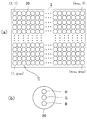
- FIG. (A) is a front view schematically showing a plurality of light emitting element portions provided in the display shown in FIG. 1, and (b) is an enlarged view schematically showing the structure of one light emitting element unit.
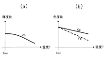
- Is. (A) and (b) are diagrams showing an example of changes in brightness and chromaticity of light generated in a light emitting element unit having a plurality of LEDs depending on temperature.
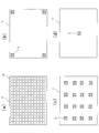
- FIG. 1 It is a block diagram which shows the structure of the temperature compensation part of the image processing apparatus shown in FIG. (A) and (b) are diagrams showing an example of the relationship between the input and the output defined in the compensation table stored in the compensation table storage unit shown in FIG. It is a flowchart which shows the process which the image processing apparatus shown in FIG. 1 performs. It is a block diagram which shows the image display apparatus which concerns on Embodiment 1 together with a learning apparatus and a learning temperature measuring part. (A) to (d) are diagrams showing an installation example of the temperature measuring unit shown in FIG. It is a block diagram which shows the structure of the image display device which concerns on Embodiment 2.
- FIG. 1 It is a figure which shows the example of the neural network which constitutes the temperature estimation part of the image processing apparatus shown in FIG. It is a flowchart which shows the process which the image display apparatus which concerns on Embodiment 2 performs. It is a block diagram which shows the structure of the image display device which concerns on Embodiment 3. FIG. It is a flowchart which shows the process which the image display apparatus which concerns on Embodiment 3 performs.
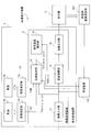
- FIG. 1 is a block diagram showing a configuration of an image display device 1 according to the first embodiment.
- the image display device 1 has a display device 2 for displaying an image and a display control device 3 for controlling the display device 2.
- the display control device 3 includes the image processing device 4, the heat sources 6a and 6b which are heat sources of the first to Nth (N is a positive integer) such as a power supply and an IC (Integrated Circuit) chip, and the temperatures of the heat sources 6a and 6b.
- It has temperature measuring units 5a and 5b, which are first to Nth temperature measuring units, respectively.
- N 2
- the number of temperature measuring units that is, N
- the number of temperature measuring units that is, N
- the number of temperature measuring units may be 3 or more.
- FIG. 2A is a front view schematically showing a plurality of light emitting element units 20 provided in the display 2 shown in FIG. 1, and FIG. 2B is a structure of one light emitting element unit 20. It is an enlarged view which shows roughly.
- the display unit 2 y in the horizontal scanning direction x max number in (lateral direction in FIG. 2 (a)), (vertical direction in FIG. 2 (a)) vertical scanning direction max
- x max and y max are predetermined positive integers.
- Each light emitting element unit 20 has, for example, an LED as a light emitting element that emits red (R), green (G), and blue (B) light.
- the LEDs that emit R, G, and B light are also referred to as “LED for R”, “LED for G”, and “LED for B”, respectively.
- the LED that emits the light of R, G, and B is also referred to as "LED for R, G, and B".
- each light emitting element unit (that is, each pixel) 20 has an LED for R, an LED for G, and an LED for B in one package. It has a structure provided with LEDs.
- the structure of the light emitting element unit 20 is not limited to the above, and may be any one having one or more light emitting elements.
- FIG. 3 (a) and 3 (b) are diagrams showing an example of changes in brightness and chromaticity of light generated in the light emitting element unit 20 having LEDs for R, G, and B depending on the temperature.
- FIG. 3A is a graph showing the luminance ratio (that is, the normalized value of luminance) Vp, which is the ratio of the luminance at the temperature T to the luminance, which is the luminance at the reference temperature Tmr.
- FIG. 3B is a graph showing the chromaticity ratio (that is, the normalized value of the chromaticity) Xp, Yp, which is the ratio of the chromaticity at the temperature T to the reference chromaticity, which is the chromaticity at the reference temperature Tmr. ing. As shown in FIGS.
- both or one of the brightness and chromaticity of the generated light depends on the temperature T. Change.
- the luminance ratio Vp decreases as the temperature T increases.
- the chromaticity is represented by x and y, which are two numerical values indicating the xy coordinates (x, y) in the CIE-xy chromaticity diagram.
- the chromaticity ratios Xp and Yp which indicate changes in the values of x and y in the CIE-xy chromaticity diagram, decrease as the temperature T increases. Note that x and y in the CIE-xy chromaticity are symbols different from (x, y) as coordinates indicating the positions of pixels on the screen of the display 2 in FIG. 2A and the like.
- the temperature measuring unit 5a is installed around (for example, in the vicinity) of the heat source 6a mounted on the image display device 1, measures the temperature of the heat source 6a, and outputs a temperature measurement value Ta0 indicating the temperature of the heat source 6a.
- the heat source 6a affects the temperature of the LED included in the light emitting element portion constituting the display 2.
- the temperature measuring unit 5b measures the temperature of the heat source 6b mounted on the image display device 1 and outputs the temperature measured value TaN.
- the number of temperature measuring units is two will be described.
- the temperature measuring units 5a and 5b has a temperature sensor.
- the temperature sensor may be a contact type or a non-contact type.
- the contact type temperature sensor is composed of, for example, a thermistor or a thermocouple.
- the non-contact temperature sensor receives, for example, infrared rays and detects the surface temperature.
- the image processing device 4 causes the display 2 to display an image corresponding to the input image data.
- the image processing device 4 estimates the temperature of each light emitting element unit (that is, the pixel of the coordinates (x, y)) 20 of the display 2 based on the input image data, and the temperature estimation value Te0 which is the estimated temperature. Based on (x, y), image data for compensating for changes in brightness and chromaticity of light generated in the light emitting element unit 20 at coordinates (x, y) due to temperature changes (for example, image data for each pixel). Is corrected, and the corrected image data is supplied to the display 2.
- the image processing device 4 may be partially or wholly composed of a processing circuit.
- the functions of the plurality of parts of the image processing device 4 may be realized by separate processing circuits, or the functions of the plurality of parts of the image processing device 4 may be collectively realized by one processing circuit. ..
- the processing circuit may be configured by hardware or may be configured by a computer that executes a program as software.
- a part of the functions of the image processing apparatus 4 may be realized by hardware, and the other part may be realized by a computer that executes a program as software.
- FIG. 4 is a block diagram showing a computer 9 that realizes the functions of the image processing device 4, together with a display 2 and temperature measuring units 5a and 5b.
- the computer 9 has a processor 91 as an information processing unit and a memory 92 as a storage unit.
- the processor 91 includes, for example, a CPU (Central Processing Unit), a GPU (Graphics Processing Unit), a microprocessor, a microprocessor, a DSP (Digital Signal Processor), and the like.
- a CPU Central Processing Unit
- GPU Graphics Processing Unit
- microprocessor a microprocessor
- DSP Digital Signal Processor
- the memory 92 is, for example, a RAM (Random Access Memory), a ROM (Read Only Memory), a flash memory, an EPROM (Erasable Programmable Read Only Memory), or an EEPROM (Electrically Memory Memory) with an EEPROM (Electrically Memory) .
- the memory 92 may include a magnetic disk, an optical disk, a magneto-optical disk, or the like.
- the processor 91 realizes the function of the image processing device 4 by executing the program stored in the memory 92.
- the function of the image processing device 4 includes the control of the display operation in the display device 2.
- the computer 9 shown in FIG. 4 includes a single processor 91, but may include two or more processors.
- FIG. 1 shows a functional block constituting the image processing device 4.
- the image processing device 4 includes an image input unit 11, a temperature estimation unit 12, an estimated temperature storage unit 13, a temperature compensation unit 14, and an image output unit 15.
- the image input unit 11 is a digital interface that receives digital image data Di as input image data and outputs it as image data Da.
- the image input unit 11 may be configured by an A / D converter that converts an analog image signal based on the input image data into digital image data.
- the input image data has a pixel value (that is, a component value) corresponding to the luminance value of the LEDs (that is, sub-pixels) for R, G, and B for each light emitting element unit (that is, for each pixel).
- the temperature estimation unit 12 sequentially selects a light emitting element unit (that is, a light emitting element unit to be estimated) from the plurality of light emitting element units (that is, a plurality of pixels) 20 of the display 2, and the selected light emitting element unit.
- the temperature of the above is estimated, and the temperature estimation value Te0 indicating the estimated temperature is output.
- the temperature estimation value Te0 of the light emitting element unit at the position of the coordinates (x, y) is represented by Te0 (x, y).
- Te0 (x, y) represents the position in the horizontal scanning direction in the screen of the display 2
- "y" represents the position in the screen of the display 2. Represents the position in the vertical operation direction.
- “X” in the coordinates (x, y) is 1 in the light emitting element portion at the left end of the screen and x max in the light emitting element portion at the right end of the screen.
- “Y” in the coordinates (x, y) is 1 in the light emitting element portion at the upper end of the screen and y max in the light emitting element portion at the lower end of the screen. Therefore, the position of the light emitting element portion in the upper left corner of the screen is represented by the coordinates (1, 1), and the position of the light emitting element portion in the lower right corner of the screen is represented by the coordinates (x max , y max ).
- the x and y in the coordinates (x, y) change by 1 for each pixel pitch.
- the estimated temperature storage unit 13 stores the temperature estimated value Te0 (x, y) output from the temperature estimation unit 12, delays the image data by one frame period, and delays the “temperature estimated value one frame before” Te1 (x, y). Output as y).
- the temperature estimation value Te0 (x, y) output from the temperature estimation unit 12 has no delay in one frame period with respect to the temperature estimation value Te1 (x, y) output from the estimation temperature storage unit 13. Therefore, it is called "the temperature estimate of the current frame”.
- the estimated temperature storage unit 13 outputs the temperature estimated value Te1 (x, y) delayed by one frame period.
- the estimated temperature storage unit 13 instead of outputting the estimated temperature value Te1 (x, y) delayed by one frame period, the estimated temperature storage unit 13 has an F frame period (F is) from the temperature estimated value Te1 (x, y) delayed by one frame period. (2 or more integers) F temperature estimation values Te1 (x, y) to TeF (x, y) up to the delayed temperature estimation value TeF (x, y) may be generated and output.
- the temperature estimates Te0 (x, y) to TeF (x, y) are estimates at different frame periods, that is, at different times, the sum of these is referred to as “multiple frame temperature estimates” or. Also called “temperature estimate at multiple times”. Further, the temperature estimated value Te0 (x, y) of the current frame is also referred to as “current temperature estimated value”. Further, the temperature estimates Te1 (x, y) to TeF (x, y) one frame or more before are also referred to as "past temperature estimates”.
- the temperature estimation unit 12 estimates the temperature of each of the plurality of light emitting element units 20 constituting the display 2. For example, for estimation, the input image data Da of the current frame output from the image input unit 11, the temperature measurement values Ta0 and TaN of the current frame output from the temperature measurement units 5a and 5b, and the structural position information C0 are used. The temperature estimated value Te1 one frame before output from the estimated temperature storage unit 13 is used. The temperature estimation value of the light emitting element unit to be estimated among the plurality of light emitting element units is between the image data of the light emitting element unit to be estimated, the temperature measurement value, and the light emitting element unit and the temperature measurement unit to be estimated. Learning result obtained by learning the relationship between the structural position information C0 including the information indicating the positional relationship and the measured value of the temperature of the light emitting element portion in the predetermined region including the light emitting element portion to be estimated. Estimated based on.
- the temperature estimation unit 12 sequentially selects the light emitting element unit to be estimated from the plurality of light emitting element units 20 constituting the display 2, and estimates the temperature of the selected light emitting element unit.
- the structural position information C0 includes information indicating the positions of the temperature measuring units 5a and 5b with respect to the plurality of light emitting element units 20.
- the structural position information C0 includes, for example, relative position information (that is, positional relationship) between the positions of the temperature measuring units 5a and 5b and the position of the light emitting element unit to be temperature-estimated, position information of the temperature measuring units 5a and 5b, and the like. Any can be included.
- the image data of the light emitting element portion in the peripheral region of the light emitting element portion of the input image data Da is also used, and the temperature estimation value Te1 one frame before is used.
- the temperature estimation value for the light emitting element portion in the peripheral region of the light emitting element portion is also used.
- the range in which the coordinates are represented by (x ⁇ ⁇ , y ⁇ ⁇ ) is the peripheral region of the selected light emitting element unit. It is said that.
- ⁇ ⁇ is the range from ⁇ max to + ⁇ max
- ⁇ ⁇ is the range from ⁇ max to + ⁇ max.
- each of ⁇ max and ⁇ max is a predetermined value, and is, for example, about 2 to 10. It should be noted that ⁇ max and ⁇ max may have the same value or different values.
- the peripheral region for the temperature estimated value Te1 one frame before may be narrower than the peripheral region for the temperature estimated value Te0 of the input image data Da. That is, ⁇ max (1) ⁇ max (0) and ⁇ max (1) ⁇ max (0) may be set.
- ⁇ max (F) ⁇ max (F-1) and ⁇ max (F) ⁇ max (F-1) may be set.
- the temperature estimation unit 12 includes image data Da (x ⁇ ⁇ , y ⁇ ⁇ ), past temperature estimation values Te1 (x ⁇ ⁇ , y ⁇ ⁇ ), and current frames output from temperature measurement units 5a and 5b. Based on the temperature measurement values Ta0 and TaN and the structural position information C0, the temperature estimation value Te0 (x, y) of the selected light emitting element unit is obtained.
- the temperature estimation unit 12 is composed of, for example, a multi-layer neural network. FIG. 5 shows an example of such a neural network 25.
- the neural network 25 shown in FIG. 5 has an input layer 251, an intermediate layer (that is, a hidden layer) 252, and an output layer 253.
- the number of intermediate layers is 3, but the number of intermediate layers may be 2 or less or 4 or more.
- Each of the neurons P of the input layer 251 has a structural position information C0, a temperature measurement value Ta0, TaN, and a past temperature estimation value Te1 (x ⁇ ⁇ , y ⁇ ⁇ ), that is, the temperature of each of the plurality of light emitting element units 20.
- One of the estimated value and the input image data Da (x ⁇ ⁇ , y ⁇ ⁇ ), that is, the image data (that is, the pixel value) of each of the plurality of light emitting element units 20 is assigned, and each neuron P is assigned.
- the given values (lighting rate, temperature measurement value, temperature estimation value, and input image data) are input.
- the neuron P of the input layer 251 outputs the input as it is.
- the neuron P of the output layer 253 is composed of a plurality of bits, for example, 10 bits, and outputs data indicating the temperature estimation value Te0 (x, y) of the selected light emitting element unit.
- Each of the neurons P in the intermediate layer 252 and the output layer 253 performs an operation represented by the following model formula (1) for a plurality of inputs.
- N is the number of inputs to neuron P.
- the number of inputs to neuron P is not necessarily the same among neurons.
- x 1 to x N indicate the input data of the neuron P
- w 1 to w N indicate the weight for the input data x 1 to x N
- b indicates the bias.
- the weights w 1 to w N and the bias b are determined by learning. Further, the weights w 1 to w N and the bias b are collectively referred to as parameters.
- the function s (a) is an activation function.
- the activation function may be, for example, a step function that outputs 0 if a is 0 or less, and outputs 1 otherwise.
- the activation function s (a) may be a ReLU (Rectifier Liner Unit) function that outputs 0 if a is 0 or less, and outputs an input value a otherwise, and the input value a is used as it is. It may be an equal function as an output value, or it may be a jigmoid function.
- the activation function used by the neuron P of the input layer 251 is an identity function.
- the step function or the jigmoid function may be used in the intermediate layer 252, and the ReLU function may be used in the output layer.
- different activation functions may be used between neurons P in the same layer.
- the number of neurons P and the number of layers are not limited to the example shown in FIG.
- the temperature compensation unit 14 corrects the image data Da supplied from the image input unit 11 according to the temperature estimation value Te0 (x, y), which is the temperature estimated by the temperature estimation unit 12, and the corrected image data. Output Db. This correction is performed on a pixel-by-pixel basis. This correction is a correction for canceling changes in luminance and chromaticity due to changes in the temperature of the light emitting element unit 20, and is performed for compensation for changes in luminance and chromaticity.
- FIG. 6 is a block diagram showing the configuration of the temperature compensation unit 14 of the image processing device 4 shown in FIG.
- the temperature compensation unit 14 has, for example, a compensation table storage unit 141, a coefficient reading unit 142, and a coefficient multiplication unit 143.
- the compensation table storage unit 141 stores a compensation table which is compensation information for compensating for changes in luminance and chromaticity due to temperature.
- 7 (a) and 7 (b) are diagrams showing an example of the relationship between the input and the output defined in the compensation table stored in the compensation table storage unit 141.
- the relationship between the input and the output here is expressed by the ratio of the output to the input, that is, a coefficient. This coefficient is called a compensation coefficient.
- the compensation table for luminance is one having an input-output relationship shown in FIG. 7A, that is, It is stored that the change with respect to the increase in temperature T is in the opposite direction to the luminance ratio Vp shown in FIG. 3 (a).
- a value equal to the reciprocal of the normalized value of the luminance ratio Vp is stored in the compensation table as the compensation coefficient Vq.
- the coefficient reading unit 142 uses the temperature estimation value Te0 (x, y) of each light emitting element unit 20 to refer to the compensation table stored in the compensation table storage unit 141, whereby the temperature of each light emitting element unit 20 is reached.
- the compensation coefficient Vq (x, y) corresponding to the estimated value Te0 (x, y) is read out, and the read compensation coefficient is supplied to the coefficient multiplication unit 143.
- the coefficient multiplication unit 143 corrects the read compensation coefficient Vq (x, y) by multiplying the input image data Da (x, y), and corrects the image data Db (x, y). That is, the compensated image data Db (x, y) corresponding to the input image data Da (x, y) is generated and output.
- the compensation table storage unit 141 stores the compensation table composed of the compensation coefficients for correcting the brightness, but instead, the components for correcting the brightness and the chromaticity, that is, the components of R, G, and B. You may keep a compensation table consisting of compensation coefficients for correcting each of the values.
- the compensation table is the input shown in FIG. 7 (b).
- Those having an output relationship, that is, those in which the change with respect to the increase in temperature T is opposite to the chromaticity ratios Xp and Yp shown in FIG. 3B are stored.
- a value equal to the reciprocal of the chromaticity ratio Xp of the x component of the chromaticity is stored in the compensation table as the compensation coefficient Xq
- a value equal to the reciprocal of the chromaticity ratio Yp of the y component of the chromaticity is the compensation table as the compensation coefficient Yq. It is stored in.
- the compensation table stores a transformation matrix of 3 ⁇ 3 as a compensation coefficient XYq (x, y) to be multiplied by the input RGB image data.
- the coefficient reading unit 142 uses the temperature estimation value Te0 (x, y) of each light emitting element unit 20 to refer to the compensation table stored in the compensation table storage unit 141, whereby the temperature of each light emitting element unit 20 is reached.
- the brightness compensation coefficient VRq (x, y) of the LED for R corresponding to the estimated value Te0 (x, y)
- the brightness compensation coefficient VGq (x, y) of the LED for G corresponding to the estimated value Te0 (x, y)
- the brightness compensation coefficient VBq of the LED for B (X, y)
- the compensation coefficient XYq (x, y) of the luminance is read, and the read compensation coefficient is supplied to the coefficient multiplication unit 143.
- the coefficient multiplying unit 143 calculates the read brightness compensation coefficients VRq (x, y), VGq (x, y), VBq (x, y), XYq (x, y) of the LEDs for R, G, and B.
- R, G, B LED image data DRa (x, y), DGa (x, y), DBa (x, y) are corrected by multiplying them, respectively, and the corrected R, G, B Image data DRb (x, y), DGb (x, y), DBb (x, y) of the LED for use is generated and output. This process is represented by the following equation (2).
- the coefficient reading unit 142 uses the temperature estimation value Te0 (x, y) of each light emitting element unit 20 to refer to the compensation table stored in the compensation table storage unit 141. Input gradation values of R, G, and B corresponding to the temperature estimation value Te0 (x, y) of each light emitting element unit 20 The colors of Ri, Gi, and Bi are converted and the gradation values of R, G, and B are output.
- the table VRGB (Ri, Gi, Bi) to be used is supplied to the coefficient multiplication unit 143.
- the coefficient multiplication unit 143 corrects with reference to the conversion table VRGB based on the input image data DRa (x, y), DGa (x, y), and DBa (x, y) of R, G, and B. Later R, G, B image data DRb (x, y), DGb (x, y), DBb (x, y) are generated and output.
- the way in which the brightness and chromaticity change depending on the temperature T may differ between the light emitting elements.
- a curve showing an average change as a curve showing the luminance ratio Vp and the chromaticity ratio Xp, Yp shown in FIGS. 3 (a) and 3 (b).
- a value obtained by averaging changes in a plurality of light emitting element units 20 is used, and a compensation table representing the compensation coefficients of FIGS. 7A and 7B is used to compensate for such average changes. Is desirable to be created.
- a different compensation table may be used for each light emitting element unit. Further, a different compensation table may be used for each of the LEDs for R, G, and B.
- the compensation table has a compensation coefficient value for each of the possible values of the temperature estimation value Te0 of the light emitting element unit, but the compensation table is not limited to this. That is, for the temperature estimation value Te0 of the light emitting element portion which has the compensation coefficient value discretely with respect to the temperature estimation value Te0 of the light emitting element portion and does not have the compensation coefficient value, the value of the compensation coefficient corresponding to the temperature estimation value Te0 of the light emitting element portion is obtained by interpolation. You may ask. This interpolation can be performed, for example, by using the value of the compensation coefficient corresponding to the temperature estimation value Te0 (that is, the table point) having the value of the compensation coefficient.
- the image output unit 15 converts the image data Db output from the temperature compensation unit 14 into a signal in a format that matches the display method of the display 2, and outputs the converted image signal Do. For example, when the light emitting element unit of the display 2 emits light by PWM (Pulse Width Modulation) drive, the image output unit 15 converts the gradation value of the image data into a PWM signal.
- PWM Pulse Width Modulation
- the display 2 displays an image based on the image signal Do received from the image processing device 4.
- changes in brightness and chromaticity due to temperature are compensated for each light emitting element unit (that is, a pixel) or for each LED (that is, a sub-pixel). Therefore, the luminance unevenness and the color unevenness of the image displayed on the display 2 are reduced.
- FIG. 8 is a flowchart showing a process executed by the image processing device 4 shown in FIG.
- the processing shown in FIG. 8 indicates the processing by the processor 91.
- step ST1 the image data is input to the image input unit 11, and the process by the image input unit 11 is executed.
- steps ST2 and ST3 the temperature measuring units 5a and 5b perform the first and second temperature measurement which is the temperature measurement of the heat sources 6a and 6b, and the temperature measured values Ta0 and TaN are output.
- the temperature estimation unit 12 estimates the temperature of the light emitting element unit 20.
- step ST5 the estimated temperature value is stored in the estimated temperature storage unit 13.
- step ST6 temperature compensation is performed for the light emitting element unit selected by the temperature compensation unit 14, and in step ST7, image data is output by the image output unit 15.
- the neural network 25 shown in FIG. 5 is generated by machine learning.
- the learning device for machine learning is used by being connected to the image display device 1 of FIG.
- FIG. 9 is a block diagram showing the image display device 1 according to the first embodiment together with the learning device 101 and the learning temperature measuring unit 102.
- the learning temperature measuring unit 102 has one or more temperature sensors. Each of the one or more temperature sensors is provided corresponding to one or more light emitting element units of the plurality of light emitting element units 20 constituting the display 2, and each temperature sensor is provided in the corresponding light emitting element unit. The temperature is measured and the measured temperature values Tf (1), Tf (2), ... Are acquired. Each of the temperature sensors may have the same configuration as the temperature sensor constituting the temperature measuring units 5a and 5b. Further, the learning temperature measuring unit 102 may be provided with a whole or a part thereof, for example, a temperature sensor integrally with the display 2, that is, in the housing of the display 2.
- One or more light emitting element units to be measured for temperature are specified in advance.
- a light emitting element unit located in the center of the screen may be specified, or a light emitting element unit located between the center of the screen and the peripheral portion may be specified.
- two or more light emitting elements are designated as one or more light emitting elements to be measured by temperature, for example, two or more light emitting elements located at positions separated from each other on the screen may be designated, or the screen may be designated.
- a light emitting element portion located in the center of the screen and one or more light emitting element portions located in the peripheral portion of the screen may be designated.
- the light emitting element unit designated as the target of temperature measurement is also referred to as a designated light emitting element unit.
- the average value of the temperature measurement values Tf (1), Tf (2), ... May be output as the temperature measurement value Tf.
- the number of designated light emitting element units is 1, the position of the designated light emitting element unit is represented by coordinates (x d , y d ), and the temperature measurement value of the designated light emitting element unit is Tf (x d , y d). ).
- the learning device 101 may be configured by a computer.
- the learning device 101 may be configured by the same computer.
- the computer constituting the learning device 101 may be, for example, the one shown in FIG. In that case, the function of the learning device 101 may be realized by the processor 91 executing the program stored in the memory 92.
- the learning device 101 operates a part of the image processing device 4, causes the temperature estimation unit 12 to estimate the temperature of the designated light emitting element unit, and the temperature estimation value Te0 (x d , y d ) is the temperature measurement for learning. Learning is performed so as to be close to the temperature measurement value Tf (x d , y d ) of the designated light emitting element unit obtained by the measurement in the unit 102.
- Each of the plurality of training input data sets LDS includes the input image data Da prepared for learning, the temperature measurement values Ta0 and TaN, and the temperature estimation value Te1 one frame before.
- the input image data Da the peripheral area of the specified light emitting element section (x d ⁇ ⁇ , y d ⁇ ⁇ ) image data Da (x d ⁇ ⁇ , y d ⁇ ⁇ ) of the light-emitting element portion in is used. Further, 1 as the previous frame temperature estimate Te1, peripheral area of the specified light emitting element section (x d ⁇ ⁇ , y d ⁇ ⁇ ) temperature estimate for the light emitting element portion in the Te1 (x d ⁇ ⁇ , y d ⁇ ⁇ ) is used.
- the input image data Da (x d ⁇ ⁇ , y d ⁇ ⁇ ), temperature measurements Ta0, TaN, and one frame before temperature estimate Te1 (x d ⁇ ⁇ , Y d ⁇ ⁇ ) are different.
- the learning device 101 sequentially selects a plurality of training input data set LDSs prepared in advance, inputs the selected learning input data set LDS to the image processing device 4, and is calculated by the temperature estimation unit 12.
- the temperature estimation value Te0 (x d , y d ) and the temperature measurement value Tf (x d , y d ) obtained by the measurement by the learning temperature measuring unit 102 are acquired, and the temperature estimation value Te 0 (x d , y) is acquired.
- the temperature measured value Tf (x d performs learning so as to approach the y d).
- the temperature estimation unit 12 constructs a temporary neural network with the original neural network.
- This neural network is similar to the neural network shown in FIG. 5, but each of the neurons in the middle layer and the output layer is connected to all the neurons in the previous layer.
- a set of parameters for a plurality of neurons is called a set of parameters and is represented by the code PS.
- the difference between the temperature estimation value Te0 (x d , y d ) and the temperature measurement value Tf (x d , y d ) is a predetermined threshold value using the above-mentioned original neural network.
- the parameter set PS is optimized as follows. Optimization can be performed, for example, by the error back propagation method.
- the learning device 101 prepares a plurality of sets LDS of learning input data, sets initial values of the set PS of parameters, and sequentially selects the set LDS of the plurality of set LDS of the plurality of learning input data.
- the learning device 101 inputs the selected set of learning input data LDS to the image processing device 4, and measures the temperature of the designated light emitting element unit Tf (x d , y d ) and the estimated temperature value Te 0 (x d , y).
- the difference from d ) (Te0 (x d , y d ) -Tf (x d , y d )) is obtained as the error ER.
- the learning device 101 obtains the total ES of the above error ERs for the set LDS of the plurality of training data as a cost function, and if the above cost function is larger than the threshold value, the above cost function becomes smaller. To change the parameter set PS. The learning device 101 repeats the above processing until the cost function becomes equal to or less than the threshold value.
- the parameter set PS can be changed by the gradient descent method. As the total ES of the error ER, the sum of the absolute values of the error ER or the sum of the squares of the error ER can be used.
- the image data Da (x d ⁇ ⁇ , y d ⁇ ⁇ ) input to the temperature compensation unit 14 is supplied to the display unit 2 via the image output unit 15 and used to drive the light emitting element unit of the display unit 2. ..
- the light emitting element portion outside the peripheral region of the designated light emitting element portion may or may not be driven. When driving, it may be driven by an arbitrary signal.
- Temperature estimates Te0 obtained by estimating the temperature estimation unit 12 (x d, y d) is input to the learning apparatus 101, the learning apparatus 101, the temperature estimated value Te0 (x d, y d) temperature measurement Learning is performed so as to be close to the value Tf (x d , y d).
- the learning device 101 breaks the synaptic connection (that is, the connection between neurons) at which the weight becomes zero.
- the temperature sensor of the learning temperature measuring unit 102 is removed, and the image display device 1 is used in a state where the temperature sensor is removed. That is, when used for image display, the image display device 1 does not require a temperature sensor for detecting the temperature of the light emitting element unit. This is because the temperature of the light emitting element unit can be estimated by the temperature estimation unit 12 even if there is no temperature sensor for detecting the temperature of the light emitting element unit.
- the learning device 101 may be removed or may remain attached after learning is completed.
- the function of the learning device 101 is realized by executing a program by the processor 91, the program may remain stored in the memory 92.
- the temperature of each light emitting element can be estimated based on the input image data, so that the image display device 1 measures the temperature of each light emitting element. Even if it is not provided, it is possible to compensate for changes in the brightness and chromaticity of light generated in the light emitting element portion due to temperature changes.
- the image display device 1 does not have to be provided with a temperature sensor for measuring the temperature of the light emitting element portion other than the designated light emitting element portion, and further, when displaying an image. Has the effect of being able to compensate for changes in the brightness and chromaticity of light generated in the light emitting element unit due to temperature changes without measuring the temperature of the designated light emitting element unit.
- the position of the temperature measuring unit (for example, 5a, 5b) can be set around the heat source.
- the position of the temperature measuring unit (for example, 5a, 5b) is not limited to this.
- the temperature measuring units 5 are installed at the four corners on the back side as shown in FIG. 10 (b).
- the temperature measuring units 5 may be installed at equal intervals on the back side as shown in FIG. 10 (c), or the temperature measuring units 5 may be installed in the center of the back side as shown in FIG. 10 (d). May be good.
- FIG. 11 is a block diagram showing the configuration of the image display device 1b according to the second embodiment.
- the image display device 1b includes a display device 2 and a display control device 3b.
- the display control device 3b includes an image processing device 4b, heat sources 6a and 6b such as a power supply and an IC chip, and temperature measuring units 5a and 5b for measuring the temperatures of the heat sources 6a and 6b, respectively.
- the image processing apparatus 4b shown in FIG. 11 is not provided with the estimated temperature storage unit 13 of FIG.
- the image display device 1b according to the second embodiment is the same as the image display device 1 according to the first embodiment.
- the temperature estimation unit 12 in the first embodiment is the light emitting element of the display 2 based on the structural position information C0, the input image data Da, the temperature measurement values Ta0, TaN, and the past temperature estimation value Te1. Estimate the temperature of the part.
- the temperature estimation unit 12b of the second embodiment does not use the past temperature estimation value Te1 but uses the structural position information C0, the input image data Da, the temperature measurement values Ta0, and TaN, respectively. Estimate the temperature of the light emitting element.
- FIG. 12 is a diagram showing an example of a neural network 25b constituting the temperature estimation unit 12b of the image processing apparatus 4b shown in FIG.
- the temperature estimation unit 12b is composed of, for example, a multi-layer neural network.
- the neural network 25b shown in FIG. 12 has an input layer 251b, an intermediate layer (that is, a hidden layer) 252b, and an output layer 253b, similarly to the neural network 25 shown in FIG.
- the number of intermediate layers is 3, but the number of intermediate layers may be 2 or less or 4 or more.
- the input layer 251b is generally the same as the input layer 251 of the neural network 25 shown in FIG. However, the temperature estimation value Te1 (x ⁇ ⁇ , y ⁇ ⁇ ) is not input to the input layer 251b of the neural network 25b shown in FIG. 12, and the structural position information C0 and the input image data Da (x ⁇ ⁇ , y) are not input. ⁇ ⁇ ), temperature measurement values Ta0, TaN are input.
- the neuron of the output layer 253b is composed of a plurality of bits, for example, 10 bits, like the neuron of the output layer 253 of FIG. 7, and outputs data indicating the temperature estimation value Te0 (x, y) of the light emitting element unit.
- neurons having synaptic connections for feedback are used as at least some of the neurons in the middle layer 252b.
- Each neuron P having a synaptic connection for feedback performs an operation represented by the model equation of the following equation (3) for a plurality of inputs.
- Equation (3) w 0 indicates the weight of the same neuron for the output y (t-1) one "time step" before. Equation (3) is the same as equation (1) except that the term w 0 ⁇ y (t-1) is added.
- FIG. 13 is a flowchart showing a process executed by the image display device 1b according to the second embodiment.
- FIG. 13 shows a processing procedure by the processor 91.
- step ST5 of FIG. 13 step ST4 in FIG. 6 is replaced with step ST4b.
- step ST4b the temperature of each light emitting element unit is estimated. This process is the same as the process by the temperature estimation unit 12b in FIG.
- the image display device 1b, the display control device 3b, and the image processing device 4b according to the second embodiment the same effect as that of the first embodiment can be obtained. Further, since the estimated temperature storage unit 13 used in the first embodiment is not required, there is an advantage that the configuration is simple.
- FIG. 14 is a block diagram showing the configuration of the image display device 1c according to the third embodiment.
- the image display device 1c includes a display device 2 and a display control device 3c.
- the display control device 3c includes an image processing device 4c, heat sources 6a and 6b, and temperature measuring units 5a and 5b for measuring the temperatures of the heat sources 6a and 6b, respectively.
- the image processing device 4c shown in FIG. 14 is different from the image processing device 4 of the display control device 3 shown in FIG. 1 in that it has a variation correction unit 16.
- the image display device 1c according to the third embodiment is the same as the image display device 1 according to the first embodiment.
- the variation correction unit 16 of the image processing device 4c corrects variations in at least one of the brightness and chromaticity of the light generated in each of the plurality of light emitting element units 20 of the display 2.
- the variation referred to here is a variation due to individual differences in at least one of the luminance and chromaticity of the light generated in the light emitting element portion.
- the temperature compensating unit 14 corrects the image data so as to compensate for the change in the brightness and chromaticity of the light generated in each of the plurality of light emitting element units 20 due to the temperature T.
- the variation correction unit 16 compensates for variations in luminance and chromaticity due to individual differences between the light emitting element units.
- the image data Da for the plurality of light emitting element units of the display 2 is transferred from the image input unit 11 to the variation correction unit 16, for example, in the upper left corner of the screen of the display 2 shown in FIG. 2A.
- the image data of the light emitting element unit in the lower right corner is input in order from the light emitting element unit of.
- the variation correction unit 16 treats the image data Da input at each time point as image data Da for the light emitting element unit (also referred to as “attention light emitting element unit”) to be processed. Variation correction is performed on the image data Da, and the corrected image data Db is output.
- the display 2 displays an image based on the image signal Do.
- changes in luminance and chromaticity due to temperature are compensated for each pixel, and variations in luminance and chromaticity due to individual differences in the light emitting element portion are corrected. Therefore, the display 2 displays an image with reduced luminance unevenness and color unevenness.
- FIG. 15 is a flowchart showing a process executed by the image display device 1c according to the third embodiment.
- FIG. 15 shows a processing procedure by the processor 91.
- step ST8 the variation correction unit 16 performs variation correction.
- the image display device 1c, the display control device 3c, and the image processing device 4c according to the third embodiment the same effect as that of the first embodiment can be obtained. Further, since the variation in each light emitting element unit can be corrected, the luminance unevenness and the color unevenness of the image displayed on the display 2 can be further reduced.
- one light emitting element unit is composed of three LEDs for R, G, and B has been described, but the number of LEDs constituting one light emitting element unit is three. Not limited to.
- one light emitting element unit may be composed of two or less LEDs, or may be composed of four or more LEDs.
- 3b and 3c may be any as long as they correct the image data in order to compensate for at least one of the luminance and the chromaticity. That is, the temperature compensating unit 14 may correct the image data so as to compensate for at least one of the luminance and the chromaticity due to the temperature change.
- the image display devices 1, 1b, 1c, the display control devices 3, 3b, 3c, and the image processing devices 4, 4b, 4c have been described, but the display control devices 3, 3b have been described.
- the display control method carried out in 3c and the image processing method carried out in the image processing devices 4, 4b and 4c also form a part of the present disclosure.
- a program for causing the computer 9 to execute the processing in the display control method or the image processing method and a computer-readable recording medium (for example, a non-temporary recording medium) on which the program is recorded are also included in the present disclosure. Form a part.
Landscapes
- Engineering & Computer Science (AREA)
- Physics & Mathematics (AREA)
- Computer Hardware Design (AREA)
- General Physics & Mathematics (AREA)
- Theoretical Computer Science (AREA)
- Control Of El Displays (AREA)
- Control Of Indicators Other Than Cathode Ray Tubes (AREA)
Priority Applications (2)
| Application Number | Priority Date | Filing Date | Title |
|---|---|---|---|
| PCT/JP2020/026737 WO2022009345A1 (ja) | 2020-07-08 | 2020-07-08 | 画像処理装置、表示制御装置、画像表示装置、画像処理方法、プログラム、及び記録媒体 |
| JP2022534566A JP7471416B2 (ja) | 2020-07-08 | 2020-07-08 | 画像処理装置、表示制御装置、画像表示装置、画像処理方法、プログラム、及び記録媒体 |
Applications Claiming Priority (1)
| Application Number | Priority Date | Filing Date | Title |
|---|---|---|---|
| PCT/JP2020/026737 WO2022009345A1 (ja) | 2020-07-08 | 2020-07-08 | 画像処理装置、表示制御装置、画像表示装置、画像処理方法、プログラム、及び記録媒体 |
Publications (1)
| Publication Number | Publication Date |
|---|---|
| WO2022009345A1 true WO2022009345A1 (ja) | 2022-01-13 |
Family
ID=79552473
Family Applications (1)
| Application Number | Title | Priority Date | Filing Date |
|---|---|---|---|
| PCT/JP2020/026737 Ceased WO2022009345A1 (ja) | 2020-07-08 | 2020-07-08 | 画像処理装置、表示制御装置、画像表示装置、画像処理方法、プログラム、及び記録媒体 |
Country Status (2)
| Country | Link |
|---|---|
| JP (1) | JP7471416B2 (https=) |
| WO (1) | WO2022009345A1 (https=) |
Cited By (1)
| Publication number | Priority date | Publication date | Assignee | Title |
|---|---|---|---|---|
| CN114613320A (zh) * | 2022-03-29 | 2022-06-10 | 湖北长江新型显示产业创新中心有限公司 | 显示面板及显示装置 |
Citations (4)
| Publication number | Priority date | Publication date | Assignee | Title |
|---|---|---|---|---|
| JPH08177599A (ja) * | 1994-12-28 | 1996-07-09 | Mazda Motor Corp | 車両装備物の温度推定方法及び温度推定装置 |
| US20170206834A1 (en) * | 2016-01-20 | 2017-07-20 | Samsung Display Co., Ltd. | Temperature estimating apparatus, a method of estimating a temperature, and a display system including the temperature estimating apparatus |
| US20170236490A1 (en) * | 2016-02-17 | 2017-08-17 | Samsung Display Co., Ltd. | Luminance compensator in display device |
| WO2019059000A1 (ja) * | 2017-09-25 | 2019-03-28 | Eizo株式会社 | 雰囲気温度推定装置、雰囲気温度推定方法、プログラム及びシステム |
-
2020
- 2020-07-08 WO PCT/JP2020/026737 patent/WO2022009345A1/ja not_active Ceased
- 2020-07-08 JP JP2022534566A patent/JP7471416B2/ja active Active
Patent Citations (4)
| Publication number | Priority date | Publication date | Assignee | Title |
|---|---|---|---|---|
| JPH08177599A (ja) * | 1994-12-28 | 1996-07-09 | Mazda Motor Corp | 車両装備物の温度推定方法及び温度推定装置 |
| US20170206834A1 (en) * | 2016-01-20 | 2017-07-20 | Samsung Display Co., Ltd. | Temperature estimating apparatus, a method of estimating a temperature, and a display system including the temperature estimating apparatus |
| US20170236490A1 (en) * | 2016-02-17 | 2017-08-17 | Samsung Display Co., Ltd. | Luminance compensator in display device |
| WO2019059000A1 (ja) * | 2017-09-25 | 2019-03-28 | Eizo株式会社 | 雰囲気温度推定装置、雰囲気温度推定方法、プログラム及びシステム |
Cited By (2)
| Publication number | Priority date | Publication date | Assignee | Title |
|---|---|---|---|---|
| CN114613320A (zh) * | 2022-03-29 | 2022-06-10 | 湖北长江新型显示产业创新中心有限公司 | 显示面板及显示装置 |
| CN114613320B (zh) * | 2022-03-29 | 2024-01-16 | 湖北长江新型显示产业创新中心有限公司 | 显示面板及显示装置 |
Also Published As
| Publication number | Publication date |
|---|---|
| JP7471416B2 (ja) | 2024-04-19 |
| JPWO2022009345A1 (https=) | 2022-01-13 |
Similar Documents
| Publication | Publication Date | Title |
|---|---|---|
| US20220208065A1 (en) | Image processing device, method, image display device, and recording medium | |
| US10553141B2 (en) | Compensation technique for color shift in displays | |
| KR102599600B1 (ko) | 디스플레이 장치 및 그 구동 방법 | |
| TWI498872B (zh) | 有機發光二極體顯示器中將rgb資料訊號轉換成rgbw資料訊號的方法與裝置 | |
| CN103946917B (zh) | 显示设备控制方法 | |
| US9618789B2 (en) | Planar lighting apparatus and liquid crystal display apparatus | |
| TWI427614B (zh) | 顯示器及其即時自動白平衡方法 | |
| JP2012237972A (ja) | 温度推定装置、その制御方法、及び画像表示装置 | |
| RU2636803C1 (ru) | Устройство на светодиодных элементах отображения | |
| JP6827594B2 (ja) | Led表示システムおよびled表示制御装置 | |
| US11011101B2 (en) | Method and electronic device for controlling display device based on color perceived brightness | |
| CN106169283B (zh) | Led显示装置及影像显示装置 | |
| US10885840B2 (en) | Image display apparatus | |
| KR102940633B1 (ko) | 상이한 픽셀 레이아웃들의 영역들을 포함하는 디스플레이 패널에 대한 ir 드롭 보상 | |
| US7948499B2 (en) | Color control algorithm for use in display systems | |
| US10810953B2 (en) | Field sequential image display device and image display method | |
| JP6727047B2 (ja) | 表示装置 | |
| JP7471416B2 (ja) | 画像処理装置、表示制御装置、画像表示装置、画像処理方法、プログラム、及び記録媒体 | |
| JP7275402B2 (ja) | 画像処理装置、画像表示装置、画像処理方法、及び画像処理プログラム | |
| US20190287470A1 (en) | Field sequential image display device and image display method | |
| CN111402796B (zh) | 图像处理方法以及图像处理系统 | |
| TW201926303A (zh) | 顯示裝置 | |
| WO2014141884A1 (ja) | 画像処理装置及び液晶表示装置 | |
| JP2015212803A (ja) | 画像処理装置及び画像処理方法 | |
| US20220309999A1 (en) | Image display device, display control device, image processing device, and recording medium |
Legal Events
| Date | Code | Title | Description |
|---|---|---|---|
| 121 | Ep: the epo has been informed by wipo that ep was designated in this application |
Ref document number: 20944376 Country of ref document: EP Kind code of ref document: A1 |
|
| ENP | Entry into the national phase |
Ref document number: 2022534566 Country of ref document: JP Kind code of ref document: A |
|
| NENP | Non-entry into the national phase |
Ref country code: DE |
|
| 122 | Ep: pct application non-entry in european phase |
Ref document number: 20944376 Country of ref document: EP Kind code of ref document: A1 |