WO2022004289A1 - 光検出装置、および電子機器 - Google Patents
光検出装置、および電子機器 Download PDFInfo
- Publication number
- WO2022004289A1 WO2022004289A1 PCT/JP2021/021636 JP2021021636W WO2022004289A1 WO 2022004289 A1 WO2022004289 A1 WO 2022004289A1 JP 2021021636 W JP2021021636 W JP 2021021636W WO 2022004289 A1 WO2022004289 A1 WO 2022004289A1
- Authority
- WO
- WIPO (PCT)
- Prior art keywords
- signal
- transistor
- unit
- clamp
- pixel
- Prior art date
- Legal status (The legal status is an assumption and is not a legal conclusion. Google has not performed a legal analysis and makes no representation as to the accuracy of the status listed.)
- Ceased
Links
Images











Classifications
-
- H—ELECTRICITY
- H04—ELECTRIC COMMUNICATION TECHNIQUE
- H04N—PICTORIAL COMMUNICATION, e.g. TELEVISION
- H04N25/00—Circuitry of solid-state image sensors [SSIS]; Control thereof
- H04N25/70—SSIS architectures; Circuits associated therewith
- H04N25/76—Addressed sensors, e.g. MOS or CMOS sensors
- H04N25/77—Pixel circuitry, e.g. memories, A/D converters, pixel amplifiers, shared circuits or shared components
- H04N25/772—Pixel circuitry, e.g. memories, A/D converters, pixel amplifiers, shared circuits or shared components comprising A/D, V/T, V/F, I/T or I/F converters
-
- H—ELECTRICITY
- H04—ELECTRIC COMMUNICATION TECHNIQUE
- H04N—PICTORIAL COMMUNICATION, e.g. TELEVISION
- H04N25/00—Circuitry of solid-state image sensors [SSIS]; Control thereof
- H04N25/70—SSIS architectures; Circuits associated therewith
- H04N25/76—Addressed sensors, e.g. MOS or CMOS sensors
- H04N25/78—Readout circuits for addressed sensors, e.g. output amplifiers or A/D converters
-
- H—ELECTRICITY
- H04—ELECTRIC COMMUNICATION TECHNIQUE
- H04N—PICTORIAL COMMUNICATION, e.g. TELEVISION
- H04N25/00—Circuitry of solid-state image sensors [SSIS]; Control thereof
- H04N25/70—SSIS architectures; Circuits associated therewith
- H04N25/76—Addressed sensors, e.g. MOS or CMOS sensors
- H04N25/779—Circuitry for scanning or addressing the pixel array
-
- H—ELECTRICITY
- H04—ELECTRIC COMMUNICATION TECHNIQUE
- H04N—PICTORIAL COMMUNICATION, e.g. TELEVISION
- H04N25/00—Circuitry of solid-state image sensors [SSIS]; Control thereof
- H04N25/70—SSIS architectures; Circuits associated therewith
- H04N25/79—Arrangements of circuitry being divided between different or multiple substrates, chips or circuit boards, e.g. stacked image sensors
Definitions
- the present disclosure relates to a photodetector capable of detecting light and an electronic device equipped with such a photodetector.
- Patent Document 1 discloses a signal having a lamp waveform and an image pickup apparatus that performs AD conversion based on a pixel signal. Further, Patent Document 1 discloses a technique of reducing noise included in a pixel signal by a CDS (Correlated Double Sampling) method to improve image quality.
- CDS Correlated Double Sampling
- the optical detection device is arranged in a matrix, and each of a plurality of pixels capable of generating a pixel signal, a reference signal generation unit capable of generating a reference signal, and each of the plurality of pixels.
- a first-stage amplifier circuit that is provided for each pixel train and can output a first output signal according to a comparison operation based on a pixel signal and a reference signal, and a first-stage amplifier circuit that is connected to the first-stage amplifier circuit and is connected to the first-stage amplifier circuit.
- a plurality of comparison circuits including a second-stage amplifier circuit capable of outputting a second output signal corresponding to the output first output signal, and AD conversion of a pixel signal based on the second output signal.
- the second stage amplifier circuit It includes a plurality of clamp circuits capable of selectively clamping the voltage of the second output signal from, and a control signal generator for generating a clamp control signal for each of the plurality of clamp circuits.
- the electronic device includes a photodetector, and the photodetector is configured by the photodetector according to the embodiment of the present disclosure.
- the first stage amplifier circuit responds to the comparison operation based on the pixel signal and the reference signal.
- the output signal of is output, and the second output signal corresponding to the first output signal is output from the second stage amplifier circuit.
- the voltage of the second output signal from the second stage amplifier circuit can be selectively clamped by the clamping circuit.
- Timing waveform diagram which showed the signal value as an absolute value as an example of the signal output state of the comparison part when the switch of a clamp circuit is turned off. It is a timing waveform diagram which showed the signal value as the variation component from the AZ level as an example of the signal output state of the comparison part when the switch of a clamp circuit is turned off. It is a circuit diagram which shows an example of the operation state of the comparison part in the column A when the switch of the clamp circuit is turned on. It is a circuit diagram which shows an example of the operation state of the comparison part in the column B when the switch of the clamp circuit is turned on.
- FIG. It is a block diagram which shows one configuration example of the peripheral part of the reading part in the image pickup apparatus which concerns on modification 2.
- FIG. It is a flow chart schematically showing an example of the illuminance measurement process in the image pickup apparatus which concerns on modification 2.
- FIG. It is a flow diagram which shows typically an example of the image pickup processing in the image pickup apparatus which concerns on modification 2.
- FIG. It is explanatory drawing which shows the use example of the image pickup apparatus.
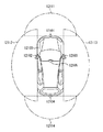
- It is a block diagram which shows an example of the schematic structure of a vehicle control system. It is explanatory drawing which shows an example of the installation position of the vehicle outside information detection unit and the image pickup unit.
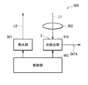
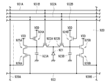
- FIG. 27 It is a block diagram which shows one structural example of the light detection part shown in FIG. 27. It is a circuit diagram which shows one configuration example of the pixel shown in FIG. 28. It is a waveform diagram which shows one operation example of the distance measuring apparatus shown in FIG. 27.
- the electronic device includes the optical detection device according to the embodiment of the present disclosure, and corresponds to, for example, a smartphone, a digital camera, a video camera, a notebook personal computer, and the like.
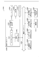
- FIG. 1 shows an example of a configuration of an image pickup apparatus 1 to which a photodetector according to an embodiment is applied.
- the image pickup apparatus 1 includes a pixel array 11, a drive unit 12, a reference signal generation unit 13, a reading unit 20, a signal processing unit 14, and an image pickup control unit 15.
- the pixel array 11 has a plurality of pixels P arranged in a matrix.
- the pixel P is configured to generate a pixel voltage Vpix according to the amount of light received.
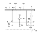
- FIG. 2 shows an example of the configuration of the pixel P in the image pickup apparatus 1.
- the pixel array 11 has a plurality of control lines TGL, a plurality of control lines RSTL, a plurality of control lines SELL, and a plurality of signal lines VSL.
- the control line TGL extends in the horizontal direction (row direction, lateral direction in FIG. 2), and one end thereof is connected to the drive unit 12.
- a control signal STG is supplied to the control line TGL by the drive unit 12.
- the control line RSTL extends in the horizontal direction, and one end thereof is connected to the drive unit 12.
- a control signal SRST is supplied to the control line RSTL by the drive unit 12.
- the control line SELL extends in the horizontal direction, and one end thereof is connected to the drive unit 12.
- a control signal SSEL is supplied to the control line SELL by the drive unit 12.
- the signal line VSL extends in the vertical direction (column direction, vertical direction in FIG. 2), and one end thereof is connected to the reading unit 20.
- This signal line VSL transmits the signal SIG generated by the pixel P to the reading unit 20.
- a plurality of pixels P for one line arranged side by side in the horizontal direction (horizontal direction in FIGS. 1 and 2) constitute a pixel line L.
- the pixel P has a photodiode PD, a transistor TG, a floating diffusion FD, and transistors RST, AMP, and SEL.
- the transistors TG, RST, AMP, and SEL are N-type MOS (Metal Oxide Semiconductor) transistors in this example.
- the photodiode PD is a photoelectric conversion element that generates an amount of electric charge according to the amount of received light and stores the generated electric charge inside.
- the anode of the photodiode PD is grounded and the cathode is connected to the source of the transistor TG.
- the gate of the transistor TG is connected to the control line TGL, the source is connected to the cathode of the photodiode PD, and the drain is connected to the floating diffusion FD.
- the floating diffusion FD is configured to store the electric charge transferred from the photodiode PD via the transistor TG.
- the floating diffusion FD is configured by using, for example, a diffusion layer formed on the surface of a semiconductor substrate. In FIG. 2, the floating diffusion FD is shown using the symbol of the capacitive element.
- the gate of the transistor RST is connected to the control line RSTL, the power supply voltage VDD is supplied to the drain, and the source is connected to the floating diffusion FD.
- the gate of the transistor AMP is connected to the floating diffusion FD, the power supply voltage VDD is supplied to the drain, and the source is connected to the drain of the transistor SEL.
- the gate of the transistor SEL is connected to the control line SELL, the drain is connected to the source of the transistor AMP, and the source is connected to the signal line VSL.
- the transistor SEL is turned on based on the control signal SSEL supplied to the control line SELL, so that the pixel P is electrically connected to the signal line VSL.
- the transistor AMP is connected to the constant current source CS (see FIG. 3 described later) of the reading unit 20 and operates as a so-called source follower.
- the pixel P outputs a signal SIG including a voltage corresponding to the voltage in the floating diffusion FD to the signal line VSL.
- the pixel P outputs the reset voltage V reset in the P phase period TP of the two periods (P phase period TP and D phase period TD) in which the reading unit 20 performs AD conversion.
- the pixel voltage Vpix corresponding to the amount of received light is output in the D phase period TD.
- the pixel P outputs a signal SIG including these reset voltage Vreset and pixel voltage Vpix to the signal line VSL.
- the drive unit 12 (FIG. 1) is configured to sequentially drive a plurality of pixels P in the pixel array 11 in pixel line L units based on an instruction from the image pickup control unit 15. Specifically, the drive unit 12 supplies a plurality of control signal STGs to a plurality of control lines TGL in the pixel array 11, respectively, supplies a plurality of control signal SRSTs to the plurality of control lines RSTL, and a plurality of control lines. By supplying a plurality of control signals SSEL to the SELL, a plurality of pixels P in the pixel array 11 are driven in units of pixel lines L.
- the reference signal generation unit 13 is configured to generate a reference signal RAMP based on an instruction from the image pickup control unit 15.
- the reference signal RAMP has a so-called lamp waveform in which the voltage level gradually changes with the passage of time in two periods (P phase period TP and D phase period TD) in which the reading unit 20 performs AD conversion.
- the reference signal generation unit 13 supplies the reference signal RAMP to the reading unit 20.
- the reading unit 20 is configured to generate the image signal DATA0 by performing AD conversion based on the signal SIG supplied from the pixel array 11 via the signal line VSL based on the instruction from the image pickup control unit 15. Will be done.
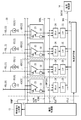
- FIG. 3 shows an example of the configuration of the reading unit 20 in the image pickup apparatus 1.
- the reading unit 20 includes a plurality of constant current sources CS (constant current sources CS [0], CS [1], CS [2], CS [2], ...) And a plurality of AD conversion units ADC (AD conversion unit ADC). [0], ADC [1], ADC [2], ADC [3] ...), and a transfer scanning unit 29.
- a plurality of constant current sources CS are provided corresponding to a plurality of signal line VSLs.
- the 0th constant current source CS [0] is provided corresponding to the 0th signal line VSL [0]
- the 1st constant current source CS [1] is the 1st signal line.
- the second constant current source CS [2] is provided corresponding to the VSL [1]
- the second constant current source CS [2] is provided corresponding to the second signal line VSL [2]
- the third constant current source CS [3] is provided. It is provided corresponding to the third signal line VSL [3].
- One end of the constant current source CS is connected to the corresponding signal line VSL and the other end is grounded.
- Each of the plurality of constant current sources CS is configured to carry a predetermined current through the corresponding signal line VSL.
- a plurality of AD conversion units ADC are provided corresponding to a plurality of signal line VSLs.
- the AD conversion unit ADC is provided for each pixel sequence of the plurality of pixels P.
- the 0th AD conversion unit ADC [0] is provided corresponding to the 0th signal line VSL [0]
- the 1st AD conversion unit ADC [1] is the 1st signal line.
- the second AD conversion unit ADC [2] is provided corresponding to the VSL [1]
- the second AD conversion unit ADC [2] is provided corresponding to the second signal line VSL [2]
- the third AD conversion unit ADC [3] is provided. It is provided corresponding to the third signal line VSL [2]. The same applies to the fourth and subsequent ones.
- Each of the plurality of AD conversion units ADC is configured to convert the voltage of the signal SIG into a digital code CODE by performing AD conversion based on the signal SIG supplied from the pixel array 11.
- the AD conversion unit ADC has a comparison unit 21, a counter 24, and a latch 25.
- the comparison unit 21 is configured to generate a signal CMPOUT by performing a comparison operation based on the reference signal RAMP supplied from the reference signal generation unit 13 and the signal SIG supplied from the pixel P via the signal line VSL. To.
- the comparison unit 21 sets an operating point based on the control signals AZSW and AZN supplied from the image pickup control unit 15, and then performs a comparison operation.
- the comparison unit 21 has a power supply circuit 22 and a comparison circuit 23.
- the image pickup control unit 15 supplies the power supply voltage VDD0 to the plurality of comparison units 21 via the power supply line VDDL.
- the power supply circuit 22 generates a power supply voltage VDD1 based on the power supply voltage VDD0, and supplies the generated power supply voltage VDD1 to the comparison circuit 23.
- the comparison unit 21 generates a signal CMPOUT by performing a comparison operation based on the reference signal RAMP and the signal SIG.
- the counter 24 performs a counting operation for counting the pulse of the clock signal CLK supplied from the image pickup control unit 15 based on the signal CMPOUT supplied from the comparison unit 21 and the control signal CTL supplied from the image pickup control unit 15. It is configured as follows.
- the latch 25 is configured to generate a digital code CODE based on the count value obtained by the counter 24 and hold the digital code CODE. Specifically, the latch 25 corresponds to the difference (CNTD-CNTP) between the count value CNTP obtained by the counter 24 in the P phase period TP and the count value CNT obtained by the counter 24 in the D phase period TD. Generate a digital code CODE. At this time, noise reduction processing by the CDS method is performed. Then, the latch 25 outputs this digital code CODE to the bus wiring BUS based on the control signal supplied from the transfer scanning unit 29.
- the transfer scanning unit 29 controls the latch 25s of the plurality of AD conversion units ADCs to sequentially output the digital code CODE to the bus wiring BUS based on the control signal CTL2 supplied from the image pickup control unit 15. It is composed of. Using this bus wiring BUS, the reading unit 20 sequentially transfers a plurality of digital code CODEs supplied from the plurality of AD conversion units ADC to the signal processing unit 14 as an image signal DATA0.
- the signal processing unit 14 (FIG. 1) generates an image signal DATA by performing predetermined signal processing on the image signal DATA0 based on an instruction from the image pickup control unit 15, and outputs the image signal DATA. It is configured as follows.
- the image pickup control unit 15 supplies control signals to the drive unit 12, the reference signal generation unit 13, the read unit 20, and the signal processing unit 14, and controls the operation of these circuits to control the operation of the image pickup device 1. It is configured to do. Specifically, the image pickup control unit 15 supplies a control signal to the drive unit 12, so that the drive unit 12 sequentially drives a plurality of pixels P in the pixel array 11 in units of pixel lines L. Control. Further, the image pickup control unit 15 controls the reference signal generation unit 13 to generate the reference signal RAMP by supplying the control signal to the reference signal generation unit 13.
- the image pickup control unit 15 supplies the power supply voltage VDD0 and the bias voltages VB1 and VB2 to the reading unit 20, and also supplies the control signals AZSW, AZN, CTL, CTL2 and the clock signal CLK to read the reading unit. 20 controls to generate the image signal DATA0 by performing AD conversion based on the signal SIG. Further, the image pickup control unit 15 controls the operation of the signal processing unit 14 by supplying a control signal to the signal processing unit 14.
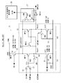
- FIG. 4A a configuration example of the comparison unit 21 is partially simplified.
- the power supply voltage VDD0, the ground voltage VSS0, and the bias voltages VB1 and VB2 are supplied to the comparison unit 21.
- the power supply voltage VDD0 is supplied from the image pickup control unit 15 via the power supply line VDDL.
- the comparison unit 21 has a power supply circuit 22 and a comparison circuit 23. Further, the comparison unit 21 has an inverter INV 10, a clamp circuit 27, and a clamp control signal generator 28.
- the power supply circuit 22 has, for example, a transistor MN10.
- the comparison circuit 23 has a first stage circuit 101 and a second stage circuit 102.
- the first-stage circuit 101 can output the signal Vout1 according to the comparison operation based on the signal SIG and the reference signal RAMP.
- the subsequent stage circuit 102 is connected to the first stage circuit 101 via the connection node Nd1, and can output the signal Vout2 corresponding to the signal Vout1 output from the first stage circuit 101 via the connection node Nd1.
- the first-stage circuit 101 includes capacitive elements C1 and C2, a transistor MP11, a constant current source 61, and a switch SW1.
- the constant current source 61 has, for example, a transistor MN11 and a capacitive element C5.
- the post-stage circuit 102 has a transistor MMN13 and another circuit 103.
- the other circuit 103 has, for example, a capacitive element C3, transistors MP12 and MN12, and a switch SW2.
- the configuration example shown in FIG. 4B will be described as an example, but the configuration of the power supply circuit 22, the constant current source 61, and the subsequent circuit 102 is not limited to the configuration example shown in FIG. 4B.
- the clamp circuit 27 has a switch SWc and a transistor MNc.
- the transistors MP11 and MP12 are P-type MOS transistors, and the transistors MN10 to MN13 and the transistors MNc are N-type MOS transistors.
- the power supply voltage VDD0 is supplied to the back gates of the transistors MP11 and MP12, and the ground voltage VSS0 is supplied to the back gates of the transistors MN10 to MN12.
- the signal SIG corresponds to a specific example of the "pixel signal” in the technique of the present disclosure.
- the signal Vout1 corresponds to a specific example of the "first output signal” in the technique of the present disclosure.
- the signal Vout2 corresponds to a specific example of the "second output signal” in the technique of the present disclosure.
- the first-stage circuit 101 corresponds to a specific example of the "first-stage amplifier circuit” in the technique of the present disclosure.
- the latter stage circuit 102 corresponds to a specific example of the "second stage amplifier circuit” in the technique of the present disclosure.
- the switch SWc corresponds to a specific example of the "switch” in the technique of the present disclosure.
- the transistor MP11 corresponds to a specific example of the "first transistor” in the technique of the present disclosure.
- the transistor MP12 corresponds to a specific example of the "second transistor” in the technique of the present disclosure.
- the capacitive element C1 corresponds to a specific example of the "first capacitive element” in the technique of the present disclosure.
- the capacitive element C2 corresponds to a specific example of the "second capacitive element” in the technique of the present disclosure.
- the transistor MN11 corresponds to a specific example of the "first load transistor” in the technique of the present disclosure.
- the transistor MN12 corresponds to a specific example of the "second load transistor” in the technique of the present disclosure.
- the P-phase period TP corresponds to a specific example of the "first period” in the technique of the present disclosure.
- the D-phase period TD corresponds to a specific example of the "second period” in the technique of the present disclosure.
- the clamp control signal generator 28 corresponds to a specific example of the "control signal generator” in the technique of the present disclosure.
- the power supply circuit 22 is provided for each comparison circuit 23 of the plurality of AD conversion units ADC, and supplies a common power supply voltage VDD1 to the first stage circuit 101 and the second stage circuit 102.
- a bias voltage VB1 is supplied to the gate of the transistor MN10, the drain is connected to the power supply line VDDL, and the source is connected to the source of the transistors MP11 and MP12 and the drain of the transistor MN13.
- the transistor MN10 operates as a so-called source follower to output a power supply voltage VDD1 from the source. Further, the source of the transistor MN10 is connected to one end of the switch SWc in the clamp circuit 27.
- Capacitive elements C1 and C2 have one end and the other end.
- One end of the capacitive element C1 is connected to the reference signal generation unit 13, and the other end is connected to the other end of the capacitive element C2, the gate of the transistor MP11, and one end of the switch SW1.
- the reference signal RAMP generated by the reference signal generation unit 13 is supplied to one end of the capacitive element C1.
- One end of the capacitive element C2 is connected to the signal line VSL, and the other end is connected to the other end of the capacitive element C1, the gate of the transistor MP11, and one end of the switch SW1.
- the signal SIG generated by the pixel P is supplied to one end of the capacitive element C2.
- At least one of the capacitive element C1 and the capacitive element C2 may have a variable capacitance. Thereby, the ratio of the capacitance between the capacitive element C1 and the capacitive element C2 may be changed.
- the gate of the transistor MP11 is connected to the other ends of the capacitive elements C1 and C2 and one end of the switch SW1 via the connection node Nd2.
- a signal SIG is input to the gate of the transistor MP11 via the capacitive element C2.
- a reference signal RAMP is input to the gate of the transistor MP11 via the capacitive element C1.
- the drain of the transistor MP11 is connected to the drain of the transistor MN11, the gate of the transistor MP12, and the other end of the switch SW1 via the connection node Nd1, and the source is connected to the source of the transistors MN10 and MP12. Further, the drain of the first transistor is connected to the source of the transistor MN13 via the connection node Nd1.
- the switch SW1 is configured to be turned on and off based on the control signal AZSW, one end of which is connected to the other end of the capacitive elements C1 and C2 and the gate of the transistor MP11 via the connection node Nd2, and the other end via the connection node Nd1. It is connected to the drain of the transistor MN11 and the gate of the transistor MP12. Further, the other end of the switch SW1 is connected to the drain of the transistor MP11. Further, the other end of the switch SW1 is connected to the source of the transistor MN13 via the connection node Nd1.
- a bias voltage VB2 is supplied to the gate of the transistor MN11.
- the drain is connected to the drain of the transistor MP11, the gate of the transistor MP12, and the other end of the switch SW1 via the connection node Nd1. Further, the drain of the transistor MN11 is connected to the source of the transistor MN13 via the connection node Nd1.
- a ground voltage VSS0 is supplied to the source of the transistor MN11.
- the transistor MN11 is a load transistor that serves as a load for the transistor MP11, and operates as a constant current source.
- the capacitive element C5 is connected to the gate of the transistor MN11, and the ground voltage VSS0 is supplied to the other end.
- the capacitive element C5 may be configured by using a MOS capacitor or the like, or may be configured by using, for example, the parasitic capacitance of the gate of the transistor MN11, the parasitic capacitance of the wiring, or the like.
- the capacitive element C5 constitutes a sample hold circuit.
- the gate of the transistor MP12 is connected to the drain of the transistor MP11, MN11 and the other end of the switch SW1 via the connection node Nd1, the drain is connected to the drain of the transistor MN12 and one end of the switch SW2, and the source is the transistor MN10, MP11. Connected to the source. Further, the drain of the transistor MP12 is connected to the gate of the transistor MN13.
- the gate of the transistor MN12 is connected to one end of the capacitive element C3 and the other end of the switch SW2, the drain is connected to the drain of the transistor MP12 and one end of the switch SW2, and the ground voltage VSS0 is supplied to the source.
- the transistor MN12 is a load transistor that serves as a load for the transistor MP12, and operates as a constant current source.
- the signal Vout2 is supplied to the gate, the drain is connected to the source of the transistors MN10, MP11, MP12, and the source is connected to the drain of the transistors MP11, MN11, the gate of the transistor MP12, and the other end of the switch SW1. ..
- the transistor MN13 controls the drain voltage of the transistor MN11 operating as a constant current source so as not to become too low based on the voltage of the signal Vout2. Thereby, for example, the constant current property of the transistor MN11 can be maintained, and the interference between the plurality of AD conversion units ADC can be suppressed.
- the switch SW2 is configured to be turned on and off based on the control signal AZN, one end is connected to the drain of the transistors MP12 and MN12, and the other end is connected to the gate of the transistor MN12 and one end of the capacitive element C3. Further, one end of the switch SW2 is connected to the gate of the transistor MN13.
- the capacitive element C3 is connected to the gate of the transistor MN12 and the other end of the switch SW2, and the ground voltage VSS0 is supplied to the other end.
- the capacitive element C3 may be configured by using a MOS capacitor or the like, or may be configured by using, for example, the parasitic capacitance of the gate of the transistor MN12, the parasitic capacitance of the switch SW2, the parasitic capacitance of the wiring, or the like.
- the power supply circuit 22 In the comparison unit 21, the power supply circuit 22 generates the power supply voltage VDD1, and the comparison circuit 23 operates based on the power supply voltage VDD1 to perform a comparison operation based on the signal SIG and the reference signal RAMP. Specifically, the current Id generated by the transistor MN11 operating as a constant current source flows through the transistor MN10, and the transistor MN10 operates as a so-called source follower. As a result, the power supply circuit 22 generates the power supply voltage VDD1. In the comparison circuit 23, as will be described later, the operating point is set by turning on the switches SW1 and SW2.
- the comparison circuit 23 performs a comparison operation based on the reset voltage Vreset included in the reference signal RAMP and the signal SIG in the P phase period TP, and is included in the reference signal RAMP and the signal SIG in the D phase period TD.
- the comparison operation is performed based on the pixel voltage Vpix.
- the inverter INV10 has an input end and an output end.
- the inverter INV10 is provided for each comparison circuit 23 of the plurality of AD conversion units ADC, and outputs a signal CMPOUT in which the signal Vout2 output from the subsequent circuit 102 is inverted.
- the clamp circuit 27 is connected to the input end and the output end of the inverter INV10.
- the clamp circuit 27 is provided for each comparison circuit 23 of the plurality of AD conversion units ADC.
- the switch SWc of the clamp circuit 27 is on / off controlled based on the clamp control signal CLSW.
- the clamp circuit 27 can selectively clamp the voltage of the signal Vout2 output from the subsequent circuit 102 by turning on the switch SWc.
- the gate of the transistor MNc in the clamp circuit 27 is connected to the output end of the inverter INV10, and the signal CMPOUT is input.
- the source of the transistor MNc is connected to the input end of the inverter INV10, the drains of the transistors MP12 and MN12, the gate of the transistor MN13, and one end of the switch SW2.
- the drain of the transistor MNc is connected to the other end of the switch SWc.
- One end of the switch SWc in the clamp circuit 27 is connected to the source of the transistor MN10, the source of the transistors MP11 and MP12, and the drain of the transistor MN13.
- the other end of the switch SWc is connected to the drain of the transistor MNc in the clamp circuit 27.
- the clamp control signal generator 28 generates a clamp control signal CLSW for the comparison circuit 23 in each of the plurality of AD conversion units ADC.
- the control signal generation unit 28 may generate the clamp control signal CLSW based on the AD conversion gain of each of the plurality of AD conversion units ADC.
- Each of the plurality of pixels P outputs a signal SIG that becomes a reset voltage V reset in the P phase period TP as a pixel signal, and then outputs a signal SIG that becomes a pixel voltage Vpix according to the received light amount in the D phase period TD.
- the reference signal generation unit 13 generates a reference signal RAMP having a predetermined reference voltage (AZ voltage) in a predetermined period before the start of the P-phase period TP and a predetermined period before the start of the D-phase period TD.
- the control signal generation unit 28 is such that the switch of the clamp circuit 27 is turned on in synchronization with the end timing of a predetermined period that becomes a predetermined reference voltage (AZ voltage), as will be described later.
- a signal may be generated.
- FIG. 5 shows a first modification of the clamp circuit 27.
- the clamp circuit 27A according to the first modification has a switch SWc and a logic gate AND1.
- the logic gate AND1 is an AND gate and has a first input terminal, a second input terminal, and an output terminal.
- the clamp control signal CLSW from the clamp control signal generator 28 is input to the first input terminal of the logic gate AND1.
- the signal CMPOUT is input to the second input terminal of the logic gate AND1.
- the switch SWc is on / off controlled by the output signal from the output terminal of the logic gate AND1.
- one end of the switch SWc is connected to the source of the transistor MN10, the source of the transistors MP11 and MP12, and the drain of the transistor MN13.
- the other end of the switch SWc is connected to the input end of the inverter INV10, the drain of the transistors MP12 and MN12, the gate of the transistor MN13, and one end of the switch SW2.
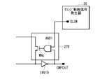
- FIG. 6 shows a second modification of the clamp circuit 27.
- the clamp circuit 27B according to the second modification has a transistor MNc and a logic gate AND1.
- the logic gate AND1 is an AND gate and has a first input terminal, a second input terminal, and an output terminal.
- the clamp control signal CLSW from the clamp control signal generator 28 is input to the first input terminal of the logic gate AND1.
- the signal CMPOUT is input to the second input terminal of the logic gate AND1.
- the output signal from the output terminal of the logic gate AND1 is input to the gate of the transistor MNc.
- the drain of the transistor MNc is connected to the source of the transistor MN10, the source of the transistors MP11 and MP12, and the drain of the transistor MN13.
- the source of the transistor MNc is connected to the input end of the inverter INV10, the drains of the transistors MP12 and MN12, the gate of the transistor MN13, and one end of the switch SW2.
- FIG. 7 shows an example of a truth table regarding the input / output of the logic gate AND1 of the clamp circuits 27A and 27B.
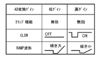
- FIG. 8 shows an example of the relationship between the AD conversion gain of the AD conversion unit ADC and the clamp function of the clamp circuit 27.
- Each of the plurality of AD conversion units ADC has an AD in a first gain mode (low gain mode) in which AD conversion is performed with the first AD conversion gain and a second AD conversion gain higher than the first AD conversion gain. It may be possible to operate in a plurality of gain modes including a second gain mode (high gain mode) for performing conversion.
- the control signal generation unit 28 may generate the clamp control signal CLSW based on the AD conversion gain of each of the plurality of AD conversion units ADC.
- the control signal generation unit 28 serves as a clamp control signal CLSW for each of the plurality of clamp circuits 27 in each of the plurality of AD conversion units ADC, and the clamp function of the clamp circuit 27 in the first gain mode (low gain mode). Is invalid, and in the second gain mode (high gain mode), a signal may be output such that the clamping function of the clamping circuit 27 is enabled.
- the slope of the signal waveform of the reference signal RAMP is relatively large in the low gain mode and small in the high gain mode.
- the slope of the signal waveform of the reference signal RAMP input to the gate of the transistor MP11 can be changed by changing the capacitance ratio between the capacitive element C1 and the capacitive element C2.
- each block shown in FIG. 1 may be formed on, for example, one semiconductor substrate or a plurality of semiconductor substrates.
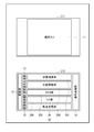
- FIG. 9 shows a mounting example of the image pickup apparatus 1 when formed on one semiconductor substrate 200.
- a pixel array 11 is arranged on the semiconductor substrate 200, and a drive unit 12 is arranged on the left side of the pixel array 11.
- a reading unit 20 is arranged below the pixel array 11.
- a constant current source unit 201 including a plurality of constant current sources CS
- a comparison circuit unit 202 including a plurality of comparison units 21, a counter unit 203 including a plurality of counters 24, and a plurality of latches 25 are provided.
- the latch portion 204 including the latch portion 204 and the transfer scanning portion 29 are arranged in this order.
- a reference signal generation unit 13 and an image pickup control unit 15 are arranged on the left side of the reading unit 20.
- a signal processing unit 14 is arranged to the right of the pixel array 11 and the reading unit 20.
- FIG. 10 shows a mounting example of the image pickup apparatus 1 when formed on two semiconductor substrates 211 and 212.
- the pixel array 11 is arranged on the semiconductor substrate 211, and the reading unit 20, the driving unit 12, the reference signal generation unit 13, the signal processing unit 14, and the image pickup control unit 15 are arranged on the semiconductor substrate 212.
- the semiconductor substrates 211 and 212 are superposed on each other.
- a plurality of signal line VSLs arranged on the semiconductor substrate 211 are electrically connected to the reading unit 20 arranged on the semiconductor substrate 212 via, for example, TSV (Through Silicon Via), and the semiconductor substrate 211 is connected.
- TSV Three Silicon Via
- a plurality of control lines TGL, RSTL, and SELL arranged in the above are electrically connected to a drive unit 12 arranged on the semiconductor substrate 212 via, for example, a TSV.
- a reading unit 20 is arranged on the semiconductor substrate 212, a driving unit 12, a reference signal generation unit 13, and an imaging control unit 15 are arranged on the left side of the reading unit 20, and a signal processing unit is arranged on the right side of the reading unit 20. 14 is arranged.
- a constant current source unit 201 including a plurality of constant current sources CS, a comparison circuit unit 202 including a plurality of comparison units 21, a counter unit 203 including a plurality of counters 24, and a plurality of latches 25 are provided in the reading unit 20, in order from the top.
- the latch portion 204 including the latch portion 204 and the transfer scanning portion 29 are arranged in this order.
- a semiconductor manufacturing process specialized in pixel formation is used by mainly arranging the pixel array 11 on the semiconductor substrate 211.
- the semiconductor substrate 211 can be manufactured. That is, since the semiconductor substrate 211 has no circuit other than the pixel array 11, for example, even if a special manufacturing process is used to form the pixels, the manufacturing process affects the circuits other than the pixel array 11. None.
- the semiconductor manufacturing process specialized in the formation of pixels can be used in the image pickup apparatus 1, the image pickup characteristics in the image pickup apparatus 1 can be improved.
- the drive unit 12 sequentially drives a plurality of pixels P in the pixel array 11 in units of pixel lines L based on an instruction from the image pickup control unit 15.
- the pixel P outputs the reset voltage Vreset as a signal SIG in the P phase period TP, and outputs the pixel voltage Vpix corresponding to the received light amount as a signal SIG in the D phase period TD.
- the reference signal generation unit 13 generates the reference signal RAMP based on the instruction from the image pickup control unit 15.
- the reading unit 20 generates the image signal DATA0 by performing AD conversion based on the signal SIG supplied from the pixel array 11 via the signal line VSL based on the instruction from the image pickup control unit 15.
- the signal processing unit 14 generates an image signal DATA by performing predetermined signal processing on the image signal DATA0 based on an instruction from the image pickup control unit 15.
- the image pickup control unit 15 supplies control signals to the drive unit 12, the reference signal generation unit 13, the read unit 20, and the signal processing unit 14, and controls the operation of these circuits to control the operation of the image pickup device 1. do
- the plurality of pixels P accumulate electric charges according to the amount of light received, and output the pixel voltage Vpix according to the amount of light received as a signal SIG. Then, the reading unit 20 performs AD conversion based on this signal SIG.
- the image pickup apparatus 1 drives the pixel array 11 to start exposure in order from the top in the vertical direction.
- the drive unit 12 sequentially selects the pixel line L by generating control signals STG and SRST, and sequentially turns on the transistors TG and RST in the pixel P for a predetermined length of time. do.
- the voltage of the floating diffusion FD and the voltage of the cathode of the photodiode PD are set to the power supply voltage VDD.
- the photodiode PD begins to accumulate electric charges according to the amount of light received. In this way, the exposure period starts sequentially in the plurality of pixels P.
- the image pickup apparatus 1 drives the pixel array 11 to read in order from the top in the vertical direction.
- the drive unit 12 sequentially selects the pixel line L by generating the control signals STG and SRST.
- the pixel P outputs the reset voltage Vreset as a signal SIG in the P-phase period TP, and outputs the pixel voltage Vpix as a signal SIG in the D-phase period TD.
- the reading unit 20 generates a digital code CODE by performing AD conversion based on this signal SIG.
- the image pickup apparatus 1 repeats such an exposure start drive and a read drive. As a result, the image pickup apparatus 1 can obtain a series of captured images.
- FIG. 11 is a circuit diagram showing an example of the operating state of the comparison unit 21 when the switch SWc of the clamp circuit 27 is turned off in the column A.
- FIG. 12 is a circuit diagram showing an example of the operating state of the comparison unit 21 when the switch SWc of the clamp circuit 27 is turned off in the column B.
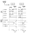
- FIG. 13 is a timing waveform diagram showing an example of the signal output state of the comparison unit 21 when the switch SWc of the clamp circuit 27 is turned off, with the signal value as an absolute value. Note that FIG. 13 mainly shows the waveform in the P phase period TP, but the same applies to the D phase period TD.
- FIG. 13 shows the voltage waveform of the control signal AZSW that controls the on / off of the switch SW1.
- (B) shows the voltage waveform of the control signal AZN that controls the switch SW2 on and off.
- (C) shows the voltage waveform of the clamp control signal CLSW that controls the switch SWc on and off.
- the control signal AZSW, the control signal AZN, and the clamp control signal CLSW are signals common to the columns A and B.
- FIG. 13 shows the current waveform of the current Id11 flowing through the transistor MN11.
- E shows the current waveform of the current Id12 flowing through the transistor MN12.
- F shows the voltage waveform of the power supply voltage VDD1 (LDOOUT) supplied from the power supply circuit 22.
- G shows the voltage waveform of the voltage Vin in the connection node Nd2 in the first stage circuit 101.
- H shows the voltage waveform of the signal Vout1 output from the first stage circuit 101.
- the voltage waveform of the signal Vout1 corresponds to the voltage waveform at the connection node Nd1.
- I shows the voltage waveform of the signal CMPOUT finally output from the comparison unit 21.
- the currents and signals shown in FIGS. 13 (D) to 13 (I) are currents and signals generated inside the comparison unit 21 in each of the columns A and B.
- the pixel P performs a reset operation to output a reset voltage Vreset, and the AD conversion unit ADC performs AD conversion based on the reset voltage Vreset in the P phase period TP. I do. Then, after that, the pixel P performs a charge transfer operation to output a pixel voltage Vpix, and the AD conversion unit ADC performs AD conversion based on the pixel voltage Vpix in the D phase period TD.
- the drive unit 12 changes the voltage of the control signal SSEL from a low level to a high level.
- the transistor SEL is turned on, and the pixel P is electrically connected to the signal line VSL.
- the drive unit 12 changes the voltage of the control signal SRST from a low level to a high level.
- the transistor RST is turned on, and the voltage of the floating diffusion FD is set to the power supply voltage VDD (reset operation).
- the pixel P outputs a voltage (reset voltage Vreset) corresponding to the voltage of the floating diffusion FD at this time. In this way, the voltage of the signal SIG becomes the reset voltage V reset.
- the reference signal generation unit 13 sets the reference signal RAMP to a predetermined reference voltage. Further, at this timing tz, the image pickup control unit 15 outputs signals for turning on both the switches SW1 and SW2 as control signals AZSW and AZN.
- the switch SW1 When the switch SW1 is turned on, the gate voltage (voltage Vin) of the transistor MP11 becomes the same voltage (AZ voltage (reference voltage)) as the drain voltage of the transistor MP11, and the voltages of the capacitive elements C1 and C2 are set.
- the switch SW2 is turned on, the gate voltage of the transistor MN12 becomes the same voltage as the drain voltage of the transistor MN12, and the voltage of the capacitive element C3 is set.
- the comparison unit 21 performs an operating point setting operation.
- This operating point setting operation is an initialization operation of the comparison unit 21, and is called an auto-zero operation.
- the period of auto-zero operation is referred to as an AZ period.
- the drive unit 12 changes the voltage of the control signal SRST from a high level to a low level. As a result, in the pixel P, the transistor RST is turned off.
- the image pickup control unit 15 outputs a signal for turning off both the switches SW1 and SW2 as control signals AZSW and AZN.
- the comparison unit 21 of the AD conversion unit ADC both the switches SW1 and SW2 are turned off, and the operating point setting operation (auto zero operation) ends.
- the comparison unit 21 operates so as to compare the gate voltage (voltage Vin) of the transistor MP11 with the AZ voltage (reference voltage).
- the reference signal generation unit 13 lowers the voltage of the reference signal RAMP below a predetermined reference voltage.
- the gate voltage (voltage Vin) of the transistor MP11 is lower than the AZ voltage (reference voltage), so that the voltage of the signal Vout1 output from the first stage circuit 101 is the AZ voltage (reference).
- the voltage is higher than the voltage).
- the AD conversion unit ADC performs AD conversion based on the reset voltage Vreset. Specifically, first, at the timing tp1, the reference signal generation unit 13 starts to increase the voltage of the reference signal RAMP from a voltage lower than a predetermined reference voltage to a predetermined degree of change. In response to this, in the comparison unit 21 of the AD conversion unit ADC, the gate voltage (voltage Vin) of the transistor MP11 begins to rise. Further, at this timing tp1, the image pickup control unit 15 starts generating the clock signal CLK. The counter 24 of the AD conversion unit ADC counts the pulse of this clock signal CLK by performing a counting operation.
- the gate voltage (voltage Vin) of the transistor MP11 exceeds the AZ voltage (reference voltage). That is, the polarity of the gate voltage of the transistor MP11 is inverted with respect to the AZ voltage.
- the reference signal generation unit 13 sets the voltage of the reference signal RAMP to a predetermined reference voltage with the end of the P-phase period TP. Further, the image pickup control unit 15 stops the generation of the clock signal CLK at this timing tp2.
- the count value of the counter 24 in the P phase period TP is CNTP.
- the latch 25 of the AD conversion unit ADC latches the count value CNTP in the P phase period TP. Then, the counter 24 is reset.
- the reference signal generation unit 13 sets the reference signal RAMP to a predetermined reference voltage (AZ voltage) again. As a result, the auto-zero operation is performed in a predetermined period before the start of the D phase period TD.
- the AD conversion unit ADC performs AD conversion based on the pixel voltage Vpix.
- the count value of the counter 24 in the D phase period TD is CNT.
- the latch 25 of the AD conversion unit ADC latches the count value CNTD in the D phase period TD. Then, the counter 24 is reset.
- the reference signal generation unit 13 sets the voltage of the reference signal RAMP to a predetermined reference voltage at the end of the D phase period TD. Further, the image pickup control unit 15 stops the generation of the clock signal CLK at this timing. Then, the drive unit 12 changes the voltage of the control signal SSEL from a high level to a low level at this timing. As a result, in the pixel P, the transistor SEL is turned off, and the pixel P is electrically separated from the signal line VSL.
- the latch 25 of the AD conversion unit ADC determines the difference (CNTD-CNTP) between the count value CNTP obtained by the counter 24 in the P phase period TP and the count value CNT obtained by the counter 24 in the D phase period TD. Generate the corresponding digital code CODE.
- FIGS. 13 (D) to 13 are currents and signals generated inside the comparison unit 21 in each of the columns A and B, but these currents and signals are for each column. Will vary. Hereinafter, this variation will be described. The same applies to the D phase period TD.
- the current Id flowing through the transistor MN10 is the sum of the current Id11 (current value Id1) flowing through the transistor MN11 and the current Id12 (current value Id2) flowing through the transistor MN12. (Current value Id1 + Id2) (FIG. 11, FIGS. 13 (D), (E)).
- the current Id flowing through the transistor MN10 is the same as the current Id11 (current value Id1) flowing through the transistor MN11 because the current Id12 flowing through the transistor MN12 is 0. 11, FIGS. 13 (D), 13 (E)). That is, when the switch of the clamp circuit 27 is turned off in the P-phase period TP, a difference occurs in the current Id between the AZ period and the P-phase period TP.
- the current value of the current Id11 flowing through the transistor MN11 has a variation of ⁇ Id1 and the current value of the current Id12 flowing through the transistor MN12 has a variation of ⁇ Id2 as compared with the column A (FIGS. 12, 13 (D), E)).
- the current value of the current Id flowing through the transistor MN10 becomes Id1 + Id2 + ⁇ Id1 + ⁇ Id2.
- the current Id flowing through the transistor MN10 in the column B is Id1 + ⁇ Id1 because the current Id12 flowing through the transistor MN12 is 0. That is, when the switch of the clamp circuit 27 is turned off in the P-phase period TP, a difference occurs in the current Id between the AZ period and the P-phase period TP.
- the power supply voltage VDD1, the voltage Vin, and the signal Vout1 also vary between the column A and the column B (FIGS. 13 (F) to (H)).
- the DC component and the AC component exist in the current and signal variations of the columns A and B described above.
- the variation of the DC component is excluded by the noise reduction processing by the CDS method. Therefore, next, the variation in the DC component for each column is excluded, and the variation amount based on the AZ level is considered.
- the variation in the AC component becomes the variation in the count value CNTP in the P phase period TP.
- FIG. 14 is a timing waveform diagram showing an example of the signal output state of the comparison unit 21 when the switch SWc of the clamp circuit 27 is turned off, showing the signal value as a variation component from the AZ level.
- 14 (A) to 14 (I) show waveforms of signals or currents similar to those of FIGS. 13 (A) to 13 (I).
- the power supply voltage VDD1 (LDOOUT) supplied from the power supply circuit 22 varies between the column A and the column B in the P-phase period TP.
- the inversion time of the signal Vout1 output from the first stage circuit 101 varies from ⁇ Vout1
- the inversion time of the signal CMPOUT finally output from the comparison unit 21 varies.
- the count value CNTP in the P phase period TP varies between the column A and the column B.
- FIG. 15 is a circuit diagram showing an example of the operating state of the comparison unit 21 when the switch SWc of the clamp circuit 27 is turned on in the column A.
- FIG. 16 is a circuit diagram showing an example of the operating state of the comparison unit 21 when the switch SWc of the clamp circuit 27 is turned on in the column B.
- FIG. 17 is a timing waveform diagram showing an example of the signal output state of the comparison unit 21 when the switch SWc of the clamp circuit 27 is turned on at a predetermined timing, with the signal value as an absolute value.
- (A) to (I) of FIG. 17 show waveforms of signals or currents similar to those of FIGS. 13 (A) to (I).
- the control signal generation unit 28 outputs a signal as the clamp control signal CLSW so that the switch of the clamp circuit 27 is turned on in synchronization with the end timing of the AZ period. As a result, in the P phase period TP (AD period), the switch of the clamp circuit 27 is turned on.
- the current Id12 having the current value Id2 flows through the transistor MN12 in the P phase period TP (AD period) as well as in the AZ period (FIG. 15, FIG. 17 (D), (E)). Therefore, in the column A, the current value of the current Id flowing through the transistor MN10 is Id1 + Id2 in both the AZ period and the P phase period TP. That is, when the switch of the clamp circuit 27 is turned on, the current Id becomes the same in the AZ period and the P phase period TP.
- the current value of the current Id11 flowing through the transistor MN11 has a variation of ⁇ Id1 and the current value of the current Id12 flowing through the transistor MN12 has a variation of ⁇ Id2 as compared with the column A (FIGS. 16 and 17 (D), E)).
- the current value of the current Id flowing through the transistor MN10 becomes Id1 + Id2 + ⁇ Id1 + ⁇ Id2 in both the AZ period and the P phase period TP. That is, when the switch of the clamp circuit 27 is turned on, the current Id becomes the same in the AZ period and the P phase period TP.
- the power supply voltage VDD1, the voltage Vin, and the signal Vout1 also vary between the column A and the column B (FIGS. 17 (F) to (H)).
- the DC component and the AC component exist in the current and signal variations of the columns A and B described above.
- the variation of the DC component is excluded by the noise reduction processing by the CDS method. Therefore, next, the variation in the DC component for each column is excluded, and the variation amount based on the AZ level is considered.
- the variation in the AC component becomes the variation in the count value CNTP in the P phase period TP.
- FIG. 18 is a timing waveform diagram showing an example of the signal output state of the comparison unit 21 when the switch SWc of the clamp circuit 27 is turned on at a predetermined timing, showing the signal value as a variation component from the AZ level.
- 18 (A) to 18 (I) show waveforms of signals or currents similar to those of FIGS. 14 (A) to 14 (I).
- the distribution width of the signal CMPOUT in the P-phase period TP can be expanded.
- the variation in the DC component of the power supply voltage VDD1 of the columns A and B is canceled by the noise reduction processing by the CDS method. This effect is particularly large when the AD conversion gain is low. On the contrary, when the AD conversion gain is high, it is small. Therefore, it is desirable to enable the clamping function of the clamping circuit 27, particularly when the AD conversion gain is high.
- the voltage of the signal Vout2 output from the subsequent circuit 102 in each of the comparison units 21 of the plurality of AD conversion units ADC is transferred by the clamp circuit 27. Since it is possible to selectively clamp, it is possible to improve the image quality.
- Modification example (Modification 1) 19A and 19B schematically show a configuration example of the comparison unit 21A according to the first modification. In FIG. 19B, a configuration example of the comparison unit 21A is partially simplified.
- the comparison unit 21 is not limited to the configuration shown in FIGS. 4A and 4B, and may be configured like the comparison unit 21A according to the modification 1 shown in FIGS. 19A and 19B.
- the ground voltage VSS0 is supplied from the image pickup control unit 15 via the ground wire VSSL.
- the comparison unit 21A has a power supply circuit 22A and a comparison circuit 23A. Further, the comparison unit 21A has an inverter INV 10, a clamp circuit 27, and a clamp control signal generator 28.
- the power supply circuit 22A has, for example, a transistor MP20.
- the comparison circuit 23A has a first stage circuit 101 and a second stage circuit 102.
- the first-stage circuit 101 can output the signal Vout1 according to the comparison operation based on the signal SIG and the reference signal RAMP.
- the subsequent stage circuit 102 is connected to the first stage circuit 101 via the connection node Nd1, and can output the signal Vout2 corresponding to the signal Vout1 output from the first stage circuit 101 via the connection node Nd1.
- the first stage circuit 101 has capacitive elements C11 and C12, a transistor MN21, a constant current source 61A, and a switch SW11.
- the constant current source 61A has, for example, a transistor MP21.
- the transistors MP20 and MP21 are P-type MOS transistors, and the transistor MN21 is an N-type MOS transistor.
- the configuration example shown in FIG. 19B will be described as an example, but the configuration of the power supply circuit 22A and the constant current source 61A is not limited to the configuration example shown in FIG. 19B.
- the subsequent circuit 102 although not shown, has, for example, a second transistor made of an N-type MOS transistor and a second load transistor made of a P-type MOS transistor.
- the power supply circuit 22A is provided for each comparison circuit 23A of the plurality of AD conversion units ADC, and supplies the ground voltage VSS1 as a common power supply voltage to the first stage circuit 101 and the second stage circuit 102.
- the bias voltage VB1 is supplied to the gate of the transistor MP20, the drain is connected to the ground line VSSL, and the source is connected to the source of the transistor MN21 and the source of the second transistor (not shown) in the subsequent circuit 102. Will be done.
- the transistor MP20 outputs the ground voltage VSS1 from the source by operating as a so-called source follower. Further, the source of the transistor MN20 is connected to one end of the switch SWc in the clamp circuit 27.
- Capacitive elements C11 and C12 have one end and the other end.
- One end of the capacitive element C11 is connected to the reference signal generation unit 13, and the other end is connected to the other end of the capacitive element C12, the gate of the transistor MN21, and one end of the switch SW11.
- the reference signal RAMP generated by the reference signal generation unit 13 is supplied to one end of the capacitive element C11.
- One end of the capacitive element C12 is connected to the signal line VSL, and the other end is connected to the other end of the capacitive element C11, the gate of the transistor MN21, and one end of the switch SW11.
- the signal SIG generated by the pixel P is supplied to one end of the capacitive element C12.
- At least one of the capacitive element C11 and the capacitive element C12 may have a variable capacitance. Thereby, the ratio of the capacitance between the capacitive element C11 and the capacitive element C12 may be changed.
- the gate of the transistor MN21 is connected to the other ends of the capacitive elements C11 and C12 and one end of the switch SW11 via the connection node Nd2.
- a signal SIG is input to the gate of the transistor MN21 via the capacitive element C12.
- a reference signal RAMP is input to the gate of the transistor MN21 via the capacitive element C11.
- the drain of the transistor MN21 is connected to the drain of the transistor MP21, the gate of the transistor MN22, and the other end of the switch SW11, and the source is connected to the transistor MP20 and the source of the second load transistor (not shown) in the subsequent circuit 102.
- the bias voltage VB2 is supplied to the gate of the transistor MP21, the drain is connected to the drain of the transistor MN21, the gate of the transistor MN22, and the other end of the switch SW11, and the power supply voltage VDD0 is supplied to the source.
- the transistor MP21 is a load transistor that serves as a load for the transistor MN21 and operates as a constant current source.
- the switch SW11 is configured to be turned on and off based on the control signal AZSW, and one end thereof is connected to the other ends of the capacitive elements C11 and C12 and the gate of the transistor MN21. The other end of the switch SW11 is connected to the drain of the transistors MN21 and MP21 and the gate of a second transistor (not shown) in the subsequent circuit 102.
- the transistor MN21 corresponds to a specific example of the "first transistor” in the technique of the present disclosure.
- the capacitive element C11 corresponds to a specific example of the "first capacitive element” in the technique of the present disclosure.
- the capacitive element C12 corresponds to a specific example of the "second capacitive element” in the technique of the present disclosure.
- the transistor MP21 corresponds to a specific example of the "first load transistor” in the technique of the present disclosure.
- the clamp circuit 27 is provided for each comparison circuit 23A of the plurality of AD conversion units ADC.
- the switch SWc of the clamp circuit 27 is on / off controlled based on the clamp control signal CLSW.
- the clamp circuit 27 can selectively clamp the voltage of the signal Vout2 output from the subsequent circuit 102 by turning on the switch SWc.
- the gate of the transistor MNc in the clamp circuit 27 is connected to the output end of the inverter INV10, and the signal CMPOUT is input.
- the source of the transistor MNc is connected to the input end of the inverter INV10 and the drain of the second transistor and the second load transistor (not shown) in the subsequent circuit 102.
- the drain of the transistor MNc is connected to the other end of the switch SWc.
- One end of the switch SWc in the clamp circuit 27 is connected to the source of the transistor MP20, the source of the transistor MN21, and the source of the second transistor (not shown) in the subsequent circuit 102.
- the other end of the switch SWc is connected to the drain of the transistor MNc in the clamp circuit 27.
- the comparison unit 21A according to the modification 1 it is possible to improve the image quality by appropriately controlling the switch SWc on and off as in the comparison unit 21 shown in FIGS. 4A and 4B.
- the configuration of the clamp circuit 27 may be configured like the clamp circuit 27A shown in FIG. 5 or the clamp circuit 27B shown in FIG.
- FIG. 20 schematically shows a configuration example of the comparison unit 21B according to the modified example 2.
- the comparison unit 21B according to the modified example 2 has a comparison circuit 23B instead of the comparison circuit 23 in the comparison unit 21 shown in FIGS. 4A and 4B.
- the comparison circuit 23B has capacitance elements Cg1, Cg2, Cg3, Cg4, and Cg5 as the capacitance element C1 and the capacitance element C2 in the comparison circuit 23 shown in FIGS. 4A and 4B. Further, the comparison circuit 23B has switches SWg1, SWg2, SWg3, SWg4, and SWg5.
- the capacitive elements Cg1, Cg2, Cg3, Cg4, and Cg5 can be connected in parallel via the switches SWg1, SWg2, SWg3, SWg4, and SWg5.
- At least one of the capacitive element C1 and the capacitive element C2 has a variable capacitance, and the ratio of the capacitance between the capacitive element C1 and the capacitive element C2 can be changed.
- the number of capacitive elements constituting the capacitive element C1 and the capacitive element C2 is not limited to this example.
- the signal SIG generated by the pixel P is supplied to one end of the capacitive element Cg1.
- the reference signal RAMP generated by the reference signal generation unit 13 is supplied to one end of the capacitive element Cg5.
- One end of the switch SWg1 is connected to one end of the capacitive element Cg1.
- the other end of the switch SWg1 is connected to one end of the capacitive element Cg2 and one end of the switch SWg2.
- the other end of the switch SWg2 is connected to one end of the capacitive element Cg3 and one end of the switch SWg3.
- the other end of the switch SWg3 is connected to one end of the capacitive element Cg4 and one end of the switch SWg4.
- the other end of the switch SWg5 is connected to one end of the capacitive element Cg5.
- the other ends of the capacitive elements Cg1, Cg2, Cg3, Cg4, and Cg5 are connected to the gate of the transistor MP11 and one end of the switch SW1.
- the capacitive elements Cg1, Cg2, Cg3, Cg4, and Cg5 may be, for example, elements having the same capacitance.
- the on / off state of the switches SWg1, SWg2, SWg3, SWg4, and SWg5 is controlled by the switch setting signal GASW. At least one of the switches SWg1, SWg2, SWg3, SWg4, and SWg5 is controlled to be in the off state. This makes it possible to change the capacitance ratio between the capacitive element C1 and the capacitive element C2.
- the slope of the signal waveform of the reference signal RAMP input to the gate of the transistor MP11 can be changed by changing the capacitance ratio between the capacitive element C1 and the capacitive element C2. This makes it possible to change the signal waveform of the reference signal RAMP into a waveform corresponding to the AD conversion gain.
- FIG. 21 shows a configuration example of a peripheral portion of the reading unit 20 in the image pickup apparatus 1 according to the modified example 2.
- the image pickup apparatus 1 according to the modification 2 further includes a gain setting control unit 81 and a register 82 with respect to the configuration example shown in FIG.
- the gain setting control unit 81 corresponds to a specific example of the "setting control unit” in the technique of the present disclosure.
- the register 82 corresponds to a specific example of the "setting storage unit” in the technique of the present disclosure.
- the signal processing unit 14 In the image pickup apparatus 1 according to the second modification, the signal processing unit 14 generates the illuminance data DATA1 based on the image signal DATA0 output from each of the plurality of AD conversion units ADC, and then generates the image signal DATA as image data. It may be generated.
- the signal processing unit 14 acquires the illuminance based on the image signal DATA0 based on the signal SIG from all or a part of the pixels P of the plurality of pixels P in the pixel array 11, and sends the illuminance data DATA1 to the gain setting control unit 81. It may be output.
- the operation for generating the illuminance data DATA1 by the signal processing unit 14 may be configured to obtain a statistic value of a predetermined pixel signal, for example, an average, a median value, and a mode value, and may be arbitrary linearly or before and after obtaining the statistic value. Non-linear operations may be performed.
- the pixel array 11 may be provided with pixels dedicated to illuminance measurement. Further, the pixel array 11 may include pixels configured to be able to switch between being used for imaging and being used for illuminance measurement.
- the register 82 may store the setting data GADT for setting the ratio of the capacitance between the capacitance element C1 and the capacitance element C2.
- the gain setting control unit 81 generates a switch setting signal GASW based on at least one of the illuminance data DATA1 from the signal processing unit 14 and the setting data GADT from the register 82, and the capacitance of the capacitance element C1 and the capacitance element C2. You may want to control the ratio of.
- the correspondence between the illuminance data DATA1 and the setting data GADT and the switch setting signal GASW may be realized by calculation hardware, calculation software, a look-up table, or the like.
- FIG. 22 schematically shows an example of the illuminance measurement process in the image pickup apparatus 1 according to the modified example 2.
- FIG. 23 schematically shows an example of an image pickup process in the image pickup apparatus 1 according to the modified example 2.
- an example of a one-frame read sequence is shown.
- the case of a rolling shutter will be described as an example.
- the drive unit 12 sequentially drives a plurality of pixels P in the pixel array 11 in units of pixel lines L based on an instruction from the image pickup control unit 15.
- the drive unit 12 selects one pixel line L (step S110).
- the drive unit 12 drives the pixel array 11 to start exposure and read out for one selected pixel line L (step S111).
- the AD conversion unit ADC performs A / D conversion on the signal SIG from the pixel P of one pixel line L (step S112).
- the AD conversion unit ADC outputs the image signal DATA0 for one pixel line L (step S113).
- the image pickup control unit 15 determines whether or not it has been driven to the final line of the pixel array 11 (step S114). If it is determined that the drive has not reached the final line (step S114: N), the image pickup control unit 15 returns to the process of step S110. When it is determined that the image pickup control unit 15 has been driven to the final line (step S114: Y), the signal processing unit 14 generates the illuminance data DATA1 based on the image signal DATA0 output from the AD conversion unit ADC. (Step S115). Next, the signal processing unit 14 outputs the illuminance data DATA1 to the gain setting control unit 81 (step S116).
- the image pickup control unit 15 performs the image pickup process of FIG. 23.
- the drive unit 12 sequentially drives a plurality of pixels P in the pixel array 11 in units of pixel lines L based on an instruction from the image pickup control unit 15.
- the drive unit 12 selects one pixel line L (step S120).
- the drive unit 12 drives the pixel array 11 to start exposure and read out for one selected pixel line L (step S121).
- the AD conversion unit ADC performs A / D conversion on the signal SIG from the pixel P of one pixel line L (step S122).
- the AD conversion unit ADC outputs the image signal DATA0 for one pixel line L (step S123).
- the image pickup control unit 15 determines whether or not it has been driven to the final line of the pixel array 11 (step S124). If it is determined that the drive has not reached the final line (step S124: N), the image pickup control unit 15 returns to the process of step S120. When it is determined that the image pickup control unit 15 has been driven to the final line (step S124: Y), the signal processing unit 14 determines that the image signal as image data is based on the image signal DATA0 output from the AD conversion unit ADC. Generate DATA (step S125). Next, the signal processing unit 14 outputs the image signal DATA as image data (step S126).
- the exposure for illuminance acquisition may be combined with the exposure for illuminance, and the illuminance data DATA1 may be generated in accordance with the generation of the image data.
- the exposure sequence for imaging and the exposure sequence for acquiring illuminance do not have to be alternated.
- the exposure sequence for acquiring the illuminance may be once every several frames.
- the generation calculation of the illuminance data DATA1 in the signal processing unit 14 may be configured with a part or all of the portion, and the gain setting control unit 81 may be configured with a chip different from other circuits.
- FIG. 24 shows a usage example of the image pickup apparatus 1 according to the above embodiment.
- the image pickup device 1 described above can be used in various cases for sensing light such as visible light, infrared light, ultraviolet light, and X-ray, as described below.
- Devices that take images for viewing such as digital cameras and portable devices with camera functions.
- Devices and user gestures used for traffic such as in-vehicle sensors that capture images of the rear, surroundings, and interior of vehicles, surveillance cameras that monitor traveling vehicles and roads, and distance measuring sensors that measure distance between vehicles.
- devices and endoscopes used in home appliances such as televisions, refrigerators, and air conditioners, and devices that perform angiography by receiving infrared light.
- Devices used for medical and healthcare such as surveillance cameras for crime prevention, cameras for person authentication, devices used for security, skin measuring instruments for taking pictures of the skin, and scalp Devices used for beauty such as microscopes for taking pictures, action cameras and wearable cameras for sports applications, devices used for sports, cameras for monitoring the condition of fields and crops, etc.
- Equipment used for agriculture such as surveillance cameras for crime prevention, cameras for person authentication, devices used for security, skin measuring instruments for taking pictures of the skin, and scalp Devices used for beauty such as microscopes for taking pictures, action cameras and wearable cameras for sports applications, devices used for sports, cameras for monitoring the condition of fields and crops, etc.
- Equipment used for agriculture such as surveillance cameras for crime prevention, cameras for person authentication, devices used for security, skin measuring instruments for taking pictures of the skin, and scalp Devices used for beauty such as microscopes for taking pictures, action cameras and wearable cameras for sports applications, devices used for sports, cameras for monitoring the condition of fields and crops, etc.
- the technology according to the present disclosure can be applied to various products.
- the technology according to the present disclosure is realized as a device mounted on a moving body of any kind such as an automobile, an electric vehicle, a hybrid electric vehicle, a motorcycle, a bicycle, a personal mobility, an airplane, a drone, a ship, and a robot. You may.
- FIG. 25 is a block diagram showing a schematic configuration example of a vehicle control system, which is an example of a mobile control system to which the technique according to the present disclosure can be applied.
- the vehicle control system 12000 includes a plurality of electronic control units connected via the communication network 12001.
- the vehicle control system 12000 includes a drive system control unit 12010, a body system control unit 12020, an outside information detection unit 12030, an in-vehicle information detection unit 12040, and an integrated control unit 12050.
- a microcomputer 12051, an audio image output unit 12052, and an in-vehicle network I / F (interface) 12053 are shown as a functional configuration of the integrated control unit 12050.
- the drive system control unit 12010 controls the operation of the device related to the drive system of the vehicle according to various programs.
- the drive system control unit 12010 has a driving force generator for generating a driving force of a vehicle such as an internal combustion engine or a driving motor, a driving force transmission mechanism for transmitting the driving force to the wheels, and a steering angle of the vehicle. It functions as a control device such as a steering mechanism for adjusting and a braking device for generating braking force of the vehicle.
- the body system control unit 12020 controls the operation of various devices mounted on the vehicle body according to various programs.
- the body system control unit 12020 functions as a keyless entry system, a smart key system, a power window device, or a control device for various lamps such as headlamps, back lamps, brake lamps, turn signals or fog lamps.
- the body system control unit 12020 may be input with radio waves transmitted from a portable device that substitutes for the key or signals of various switches.
- the body system control unit 12020 receives inputs of these radio waves or signals and controls a vehicle door lock device, a power window device, a lamp, and the like.
- the outside information detection unit 12030 detects information outside the vehicle equipped with the vehicle control system 12000.
- the image pickup unit 12031 is connected to the vehicle outside information detection unit 12030.
- the vehicle outside information detection unit 12030 causes the image pickup unit 12031 to capture an image of the outside of the vehicle and receives the captured image.
- the out-of-vehicle information detection unit 12030 may perform object detection processing or distance detection processing such as a person, a vehicle, an obstacle, a sign, or a character on the road surface based on the received image.
- the image pickup unit 12031 is an optical sensor that receives light and outputs an electric signal according to the amount of the light received.
- the image pickup unit 12031 can output an electric signal as an image or can output it as distance measurement information. Further, the light received by the image pickup unit 12031 may be visible light or invisible light such as infrared light.
- the in-vehicle information detection unit 12040 detects the in-vehicle information.
- a driver state detection unit 12041 that detects the driver's state is connected to the in-vehicle information detection unit 12040.
- the driver state detection unit 12041 includes, for example, a camera that images the driver, and the in-vehicle information detection unit 12040 determines the degree of fatigue or concentration of the driver based on the detection information input from the driver state detection unit 12041. It may be calculated, or it may be determined whether the driver has fallen asleep.
- the microcomputer 12051 calculates the control target value of the driving force generator, the steering mechanism, or the braking device based on the information inside and outside the vehicle acquired by the vehicle exterior information detection unit 12030 or the vehicle interior information detection unit 12040, and the drive system control unit.
- a control command can be output to 12010.
- the microcomputer 12051 realizes ADAS (Advanced Driver Assistance System) functions including vehicle collision avoidance or impact mitigation, follow-up driving based on inter-vehicle distance, vehicle speed maintenance driving, vehicle collision warning, vehicle lane deviation warning, and the like. It is possible to perform cooperative control for the purpose of.
- ADAS Advanced Driver Assistance System
- the microcomputer 12051 controls the driving force generating device, the steering mechanism, the braking device, and the like based on the information around the vehicle acquired by the vehicle exterior information detection unit 12030 or the vehicle interior information detection unit 12040. It is possible to perform coordinated control for the purpose of automatic driving that runs autonomously without depending on the operation.
- the microcomputer 12051 can output a control command to the body system control unit 12020 based on the information outside the vehicle acquired by the vehicle outside information detection unit 12030.
- the microcomputer 12051 controls the headlamps according to the position of the preceding vehicle or the oncoming vehicle detected by the outside information detection unit 12030, and performs cooperative control for the purpose of anti-glare such as switching the high beam to the low beam. It can be carried out.
- the audio image output unit 12052 transmits an output signal of at least one of audio and image to an output device capable of visually or audibly notifying information to the passenger or the outside of the vehicle.
- an audio speaker 12061, a display unit 12062, and an instrument panel 12063 are exemplified as output devices.
- the display unit 12062 may include, for example, at least one of an onboard display and a head-up display.
- FIG. 26 is a diagram showing an example of the installation position of the image pickup unit 12031.
- the vehicle 12100 has an imaging unit 12101, 12102, 12103, 12104, 12105 as an imaging unit 12031.
- the image pickup units 12101, 12102, 12103, 12104, 12105 are provided, for example, at positions such as the front nose, side mirrors, rear bumpers, back doors, and the upper part of the windshield in the vehicle interior of the vehicle 12100.
- the image pickup unit 12101 provided in the front nose and the image pickup section 12105 provided in the upper part of the windshield in the vehicle interior mainly acquire an image in front of the vehicle 12100.
- the image pickup units 12102 and 12103 provided in the side mirror mainly acquire images of the side of the vehicle 12100.
- the image pickup unit 12104 provided in the rear bumper or the back door mainly acquires an image of the rear of the vehicle 12100.
- the images in front acquired by the image pickup units 12101 and 12105 are mainly used for detecting a preceding vehicle, a pedestrian, an obstacle, a traffic light, a traffic sign, a lane, or the like.
- FIG. 26 shows an example of the shooting range of the imaging units 12101 to 12104.
- the imaging range 12111 indicates the imaging range of the imaging unit 12101 provided on the front nose
- the imaging ranges 12112 and 12113 indicate the imaging range of the imaging units 12102 and 12103 provided on the side mirrors, respectively
- the imaging range 12114 indicates the imaging range.
- the imaging range of the imaging unit 12104 provided on the rear bumper or the back door is shown. For example, by superimposing the image data captured by the image pickup units 12101 to 12104, a bird's-eye view image of the vehicle 12100 can be obtained.
- At least one of the image pickup units 12101 to 12104 may have a function of acquiring distance information.
- at least one of the image pickup units 12101 to 12104 may be a stereo camera including a plurality of image pickup elements, or may be an image pickup element having pixels for phase difference detection.
- the microcomputer 12051 has a distance to each three-dimensional object in the image pickup range 12111 to 12114 based on the distance information obtained from the image pickup unit 12101 to 12104, and a temporal change of this distance (relative speed with respect to the vehicle 12100). By obtaining can. Further, the microcomputer 12051 can set an inter-vehicle distance to be secured in advance in front of the preceding vehicle, and can perform automatic brake control (including follow-up stop control), automatic acceleration control (including follow-up start control), and the like. In this way, it is possible to perform coordinated control for the purpose of automatic driving or the like in which the vehicle travels autonomously without depending on the operation of the driver.
- automatic brake control including follow-up stop control
- automatic acceleration control including follow-up start control
- the microcomputer 12051 converts three-dimensional object data related to a three-dimensional object into two-wheeled vehicles, ordinary vehicles, large vehicles, pedestrians, electric poles, and other three-dimensional objects based on the distance information obtained from the image pickup units 12101 to 12104. It can be classified and extracted and used for automatic avoidance of obstacles. For example, the microcomputer 12051 distinguishes obstacles around the vehicle 12100 into obstacles that are visible to the driver of the vehicle 12100 and obstacles that are difficult to see. Then, the microcomputer 12051 determines the collision risk indicating the risk of collision with each obstacle, and when the collision risk is equal to or higher than the set value and there is a possibility of collision, the microcomputer 12051 via the audio speaker 12061 or the display unit 12062. By outputting an alarm to the driver and performing forced deceleration and avoidance steering via the drive system control unit 12010, driving support for collision avoidance can be provided.
- At least one of the image pickup units 12101 to 12104 may be an infrared camera that detects infrared rays.
- the microcomputer 12051 can recognize a pedestrian by determining whether or not a pedestrian is present in the captured image of the imaging unit 12101 to 12104.
- pedestrian recognition is, for example, a procedure for extracting feature points in an image captured by an image pickup unit 12101 to 12104 as an infrared camera, and pattern matching processing is performed on a series of feature points indicating the outline of an object to determine whether or not the pedestrian is a pedestrian. It is done by the procedure to determine.
- the audio image output unit 12052 determines the square contour line for emphasizing the recognized pedestrian.
- the display unit 12062 is controlled so as to superimpose and display. Further, the audio image output unit 12052 may control the display unit 12062 so as to display an icon or the like indicating a pedestrian at a desired position.
- the above is an example of a vehicle control system to which the technology according to the present disclosure can be applied.
- the technique according to the present disclosure can be applied to the image pickup unit 12031 among the configurations described above.
- the image quality of the captured image can be improved.
- it is possible to improve the accuracy of the vehicle collision avoidance or collision mitigation function, the follow-up driving function based on the inter-vehicle distance, the vehicle speed maintenance driving function, the vehicle collision warning function, the vehicle lane deviation warning function, and the like. can.
- FIG. 27 shows a configuration example of the ranging device 900 according to this application example.
- the distance measuring device 900 is configured to measure the distance to the object to be measured OBJ by an indirect method.
- the distance measuring device 900 includes a light emitting unit 901, an optical system 902, a photodetector unit 910, and a control unit 903.
- the light emitting unit 901 is configured to emit an optical pulse L0 toward the measurement target OBJ.
- the light emitting unit 901 emits an optical pulse L0 by performing a light emitting operation in which light emission and non-light emission are alternately repeated based on an instruction from the control unit 903.
- the light emitting unit 901 has, for example, a light source that emits infrared light. This light source is configured by using, for example, a laser light source, an LED (Light Emitting Diode), or the like.
- the optical system 902 includes a lens that forms an image on the light receiving surface S of the photodetector 910.
- An optical pulse (reflected light pulse L1) emitted from the light emitting unit 901 and reflected by the measurement object OBJ is incident on the optical system 902.
- the photodetection unit 910 is configured to generate a distance image PIC by detecting light based on an instruction from the control unit 903. Each of the plurality of pixel values included in the distance image PIC indicates a value for the distance D to the measurement target OBJ. Then, the photodetector 910 outputs the generated distance image PIC as an image signal DATA.
- the control unit 903 is configured to control the operation of the distance measuring device 900 by supplying control signals to the light emitting unit 901 and the light detection unit 910 and controlling these operations.
- FIG. 28 shows an example of the configuration of the photodetector 910.
- the photodetection unit 910 includes a pixel array 911, a drive unit 912, a reference signal generation unit 913, a reading unit 919, a signal processing unit 914, and an image pickup control unit 915.
- the pixel array 911, the drive unit 912, the reference signal generation unit 913, the read unit 919, the signal processing unit 914, and the image pickup control unit 915 may be formed on one semiconductor substrate.
- the pixel array 911 is formed on one semiconductor substrate, and the drive unit 912, the reference signal generation unit 913, the read unit 919, the signal processing unit 914, and the image pickup control unit 915 are formed on another semiconductor substrate. These two semiconductor substrates may be overlapped with each other.
- the pixel array 911 has a plurality of pixels 920 arranged in a matrix.
- the pixel 920 is configured to generate a pixel voltage Vpix according to the amount of light received.
- FIG. 29 shows an example of the configuration of the pixel 920.
- the pixel array 911 includes a plurality of control lines 931A, a plurality of control lines 931B, a plurality of control lines 932A, a plurality of control lines 932A, a plurality of control lines 933, a plurality of signal lines 939A, and a plurality of signals. It has a line 939B.
- the pixel 920 has a photodiode 921, a floating diffusion 923A, 923B, and transistors 922A, 922B, 924A, 924B, 925A, 925B, 926A, 926B.
- a circuit including a photodiode 921, a floating diffusion 923A, and transistors 922A, 924A, 925A, and 926A is also referred to as a tap A.
- a circuit including a photodiode 921, a floating diffusion 923B, and transistors 922B, 924B, 925B, and 926B is also referred to as a tap B.
- the gate of transistor 922A is connected to control line 931A, the source is connected to photodiode 921, and the drain is connected to floating diffusion 923A.
- the floating diffusion 923A is configured to store the charge supplied from the photodiode 921 via the transistor 922A.
- the gate of the transistor 924A is connected to the control line 932A, the power supply voltage VDD is supplied to the drain, and the source is connected to the floating diffusion 923A.
- the gate of the transistor 925A is connected to the floating diffusion 923A, the drain is supplied with the power supply voltage VDD, and the source is connected to the drain of the transistor 926A.
- the gate of transistor 926A is connected to control line 933, the drain is connected to the source of transistor 925A, and the source is connected to signal line 939A.
- the floating diffusion 923A is reset when the transistor 924A is turned on, and the floating diffusion 923B is reset when the transistor 924B is turned on. Then, when any one of the transistors 922A and 922B is alternately turned on, the electric charge generated by the photodiode 921 is selectively stored in the floating diffusion 923A and the floating diffusion 923B.
- the transistors 926A and 926B are turned on, the pixel 920 outputs a pixel signal corresponding to the amount of charge stored in the floating diffusion 923A to the signal line 939A, and the charge stored in the floating diffusion 923B. A pixel signal corresponding to the amount of the above is output to the signal line 939B.
- the drive unit 912 (FIG. 28) is configured to sequentially drive a plurality of pixels 920 in the pixel array 911 in pixel line L units based on an instruction from the image pickup control unit 915.
- the reference signal generation unit 913 is configured to generate a reference signal RAMP based on an instruction from the image pickup control unit 915.
- the reading unit 919 generates the image signal DATA0 by performing AD conversion based on the pixel signals supplied from the pixel array 911 via the signal lines 939A and 939B based on the instruction from the image pickup control unit 915. It is composed of.
- the signal processing unit 914 generates a distance image PIC by performing predetermined signal processing on the image signal DATA0 based on the instruction from the image pickup control unit 915, and outputs the image signal DATA including the distance image PIC. It is configured to do.
- the image pickup control unit 915 supplies control signals to the drive unit 912, the reference signal generation unit 913, the read unit 919, and the signal processing unit 914, and controls the operation of these circuits to control the operation of the light detection unit 910. Configured to control.
- FIG. 30 shows an operation example of the distance measuring device 900
- FIG. 30A shows a waveform of an optical pulse L0 emitted from a light emitting unit 901
- FIG. 30B shows an optical detection unit. The waveform of the reflected light pulse L1 detected by 910 is shown.
- the light emitting unit 901 emits an optical pulse L0 having a pulse waveform having a duty ratio of 50% based on an instruction from the control unit 903 (FIG. 30A).
- This optical pulse L0 travels toward the object to be measured OBJ.
- this light pulse L0 is reflected by the measurement object OBJ, and the reflected reflected light pulse L1 travels toward the light detection unit 910.
- the pixel 920 of the photodetector 910 detects the reflected light pulse L1 (FIG. 30 (B)).
- the reflected light pulse L1 detected by the pixel 920 has a waveform obtained by delaying the waveform of the light pulse L0 shown in FIG. 30A by the delay time DL.
- This delay time DL is the time during which the light travels in the order of the light emitting unit 901, the measurement object OBJ, and the light detection unit 910, and corresponds to the flight time of the light.
- the flight time of this light corresponds to the distance between the distance measuring device 900 and the object to be measured OBJ.
- the floating diffusion 923A of the pixel 920 accumulates a signal charge Q1 according to the amount of light received by the photodiode 921 during the period 941 in which the light emitting unit 901 emits light, and the floating diffusion 923B of the pixel 920 has the light emitting unit 901.
- the signal charge Q2 corresponding to the amount of light received by the photodiode 921 is accumulated.
- the signal processing unit 914 obtains the charge ratio between the signal charge Q1 and the signal charge Q2.
- the photodiode 921 detects light in the period 951,952, the charge amount of the signal charge Q1 is proportional to the length of the period 951, and the charge amount of the signal charge Q2 is proportional to the length of the period 952. do.
- the delay time DL is short, the signal charge Q1 increases and the signal charge Q2 decreases, and when the delay time DL is long, the signal charge Q1 decreases and the signal charge Q2 increases. In this way, the charge ratio between the signal charge Q1 and the signal charge Q2 changes according to the delay time DL.
- the delay time DL can be obtained with high accuracy, and as a result, the distance to the measurement target OBJ can be measured with high accuracy.
- the present technology can be applied to the reading unit 919. This makes it possible to improve the image quality of the distance image.
- the example of the distance measuring device 900 to which the technique according to the present disclosure can be applied has been described above.
- the technique according to the present disclosure may be applied to such a ranging device 900.
- the distance measuring device 900 can improve the image quality of the distance image.
- the pixel P is configured as shown in FIG. 2, but the pixel P is not limited to this, and pixels having various configurations can be used.
- this technology can also have the following configuration. According to this technology having the following configuration, it is possible to selectively clamp the voltage of the second output signal from the second stage amplifier circuit by the clamping circuit in each comparison circuit of a plurality of AD converters. Therefore, it is possible to improve the image quality.
- the first-stage amplifier circuit which is provided for each pixel row of the plurality of pixels and can output a first output signal according to a comparison operation based on the pixel signal and the reference signal, and the first-stage amplifier circuit.
- the second output signal includes a comparison circuit having a second stage amplifier circuit which is connected and capable of outputting a second output signal corresponding to the first output signal output from the first stage amplifier circuit.
- a plurality of AD conversion units that perform AD conversion of the pixel signal based on It has a switch which is provided for each of the comparison circuits of the plurality of AD conversion units and is controlled to be turned on and off based on a clamp control signal, and when the switch is turned on, the second stage amplifier circuit is used.
- a plurality of amplifier circuits capable of selectively clamping the voltage of the second output signal of the above, and
- a photodetector including a control signal generator that generates the clamp control signal for each of the plurality of clamp circuits.
- Each of the plurality of AD conversion units performs AD conversion in a first gain mode in which AD conversion is performed with the first AD conversion gain and a second AD conversion gain higher than the first AD conversion gain. It can operate in multiple gain modes, including 2 gain modes.
- the control signal generation unit invalidates the clamp function of the clamp circuit in the first gain mode and the clamp in the second gain mode.
- the optical detection device according to (3) above, which outputs a signal for which the clamping function of the circuit is effective.
- Each of the plurality of pixels outputs a signal having a reset voltage in the first period as the pixel signal, and then outputs a signal having a pixel voltage according to the amount of received light in the second period.
- the reference signal generation unit is adapted to generate a reference signal having a predetermined reference voltage in a predetermined period before the start of the first period and a predetermined period before the start of the second period.
- the control signal generation unit generates a signal as the clamp control signal so that the switch of the clamp circuit is turned on in synchronization with the end timing of the predetermined period (1) to (4).
- the photodetector according to any one.
- the first stage amplifier circuit is The first capacitive element to which the reference signal is input and The second capacitive element to which the pixel signal is input and It has a gate, a drain, and a source, and the reference signal is input to the gate via the first capacitive element, and the pixel signal is input to the gate via the second capacitive element.
- the first stage amplifier circuit is The photodetector according to (6) above, further comprising a first load transistor connected to the drain of the first transistor.
- At least one of the first capacitive element and the second capacitive element has a variable capacitance, and the ratio of the capacitance between the first capacitive element and the second capacitive element can be changed (6).
- the photodetector according to (7) further comprising a setting control unit that controls the ratio of the capacitance between the first capacitive element and the second capacitive element based on the illuminance data.
- a setting storage unit for storing setting data for setting the ratio of the capacitance between the first capacitive element and the second capacitive element.
- the setting control unit generates a control signal for controlling the ratio of the capacitance between the first capacitance element and the second capacitance element based on the illuminance data and the setting data (9) or ( The photodetector according to 10).
- the second stage amplifier circuit is The above (1) to (1) to have a gate, a drain, and a source, and have a second transistor in which the first output signal is input to the gate and the second output signal can be output from the drain. 11) The photodetector according to any one of.
- the second amplifier circuit is The photodetector according to (12) above, further comprising a second load transistor connected to the drain of the second transistor. (14) Further, an inverter provided for each of the comparison circuits of the plurality of AD conversion units and inverting the second output signal is provided. The photodetector according to any one of (1) to (13) above, wherein the plurality of clamp circuits are connected to an input end and an output end of the inverter, respectively.
- the photodetector is Multiple pixels arranged in a matrix, each capable of generating a pixel signal, A reference signal generator that can generate a reference signal,
- the first-stage amplifier circuit which is provided for each pixel row of the plurality of pixels and can output a first output signal according to a comparison operation based on the pixel signal and the reference signal, and the first-stage amplifier circuit.
- the second output signal includes a comparison circuit having a second stage amplifier circuit which is connected and capable of outputting a second output signal corresponding to the first output signal output from the first stage amplifier circuit.
- a plurality of AD conversion units that perform AD conversion of the pixel signal based on It has a switch which is provided for each of the comparison circuits of the plurality of AD conversion units and is controlled to be turned on and off based on a clamp control signal, and when the switch is turned on, the second stage amplifier circuit is used.
- a plurality of amplifier circuits capable of selectively clamping the voltage of the second output signal of the above, and
- An electronic device including a control signal generator that generates the clamp control signal for each of the plurality of clamp circuits.
Landscapes
- Engineering & Computer Science (AREA)
- Multimedia (AREA)
- Signal Processing (AREA)
- Transforming Light Signals Into Electric Signals (AREA)
Abstract
本開示の光検出装置は、複数の画素の各画素列ごとに設けられ、画素信号および参照信号に基づく比較動作に応じた第1の出力信号を出力可能な第1段アンプ回路と、第1段アンプ回路に接続され、第1段アンプ回路から出力された第1の出力信号に応じた第2の出力信号を出力可能な第2段アンプ回路とを有する比較回路を含み、第2の出力信号に基づいて画素信号のAD変換を行う複数のAD変換部と、複数のAD変換部のそれぞれの比較回路に対して設けられ、クランプ制御信号に基づいてオンオフ制御されるスイッチを有し、スイッチがオン状態になることにより、第2段アンプ回路からの第2の出力信号の電圧を選択的にクランプすることが可能な複数のクランプ回路と、複数のクランプ回路のそれぞれに対するクランプ制御信号を生成する制御信号発生部とを備える。
Description
本開示は、光を検出可能な光検出装置、およびそのような光検出装置を備えた電子機器に関する。
画素が受光量に応じた画素信号を生成し、AD(Analog to Digital)変換回路がその画素信号をデジタルコードに変換する光検出装置がある。光検出装置は例えば撮像装置に適用される。特許文献1には、ランプ波形を有する信号、および画素信号に基づいてAD変換を行う撮像装置が開示されている。また、特許文献1には、CDS(Correlated Double Sampling:相関2重サンプリング)法によって画素信号に含まれるノイズを低減し、画質を高める技術が開示されている。
さらなる画質の向上を図ることが可能な技術の開発が望まれている。
画質の向上を図ることが可能となる光検出装置、および電子機器を提供することが望ましい。
本開示の一実施の形態に係る光検出装置は、マトリックス状に配置され、それぞれが画素信号を生成可能な複数の画素と、参照信号を生成可能な参照信号生成部と、複数の画素の各画素列ごとに設けられ、画素信号および参照信号に基づく比較動作に応じた第1の出力信号を出力可能な第1段アンプ回路と、第1段アンプ回路に接続され、第1段アンプ回路から出力された第1の出力信号に応じた第2の出力信号を出力可能な第2段アンプ回路とを有する比較回路を含み、第2の出力信号に基づいて画素信号のAD変換を行う複数のAD変換部と、複数のAD変換部のそれぞれの比較回路に対して設けられ、クランプ制御信号に基づいてオンオフ制御されるスイッチを有し、スイッチがオン状態になることにより、第2段アンプ回路からの第2の出力信号の電圧を選択的にクランプすることが可能な複数のクランプ回路と、複数のクランプ回路のそれぞれに対するクランプ制御信号を生成する制御信号発生部とを備える。
本開示の一実施の形態に係る電子機器は、光検出装置を含み、光検出装置を、上記本開示の一実施の形態に係る光検出装置によって構成したものである。
本開示の一実施の形態に係る光検出装置、または電子機器では、複数のAD変換部のそれぞれにおける比較回路において、第1段アンプ回路から画素信号および参照信号に基づく比較動作に応じた第1の出力信号が出力され、第2段アンプ回路から第1の出力信号に応じた第2の出力信号が出力される。複数のAD変換部のそれぞれの比較回路において、第2段アンプ回路からの第2の出力信号の電圧は、クランプ回路によって選択的にクランプすることが可能となる。
以下、本開示の実施の形態について図面を参照して詳細に説明する。なお、説明は以下の順序で行う。
1.一実施の形態(光検出装置を適用した撮像装置)
1.1 構成(図1~図10)
1.2 動作および作用(図11~図18)
1.3 効果
1.4 変形例(図19A、図19B、図20~図23)
2.撮像装置の使用例(図24)
3.移動体への応用例(図25~図26)
4.測距装置への応用例(図27~図30)
5.その他の実施の形態
1.一実施の形態(光検出装置を適用した撮像装置)
1.1 構成(図1~図10)
1.2 動作および作用(図11~図18)
1.3 効果
1.4 変形例(図19A、図19B、図20~図23)
2.撮像装置の使用例(図24)
3.移動体への応用例(図25~図26)
4.測距装置への応用例(図27~図30)
5.その他の実施の形態
<1.一実施の形態(光検出装置を適用した撮像装置)>
本開示の一実施の形態に係る電子機器は、本開示の一実施の形態に係る光検出装置を含むものであり、例えば、スマートフォン、デジタルカメラ、ビデオカメラ、ノート型パーソナルコンピュータなどが該当する。
本開示の一実施の形態に係る電子機器は、本開示の一実施の形態に係る光検出装置を含むものであり、例えば、スマートフォン、デジタルカメラ、ビデオカメラ、ノート型パーソナルコンピュータなどが該当する。
ここでは、本開示の一実施の形態に係る光検出装置を撮像装置に適用した場合を例に説明する。
[1.1 構成]
図1は、一実施の形態に係る光検出装置を適用した撮像装置1の一構成例を表すものである。撮像装置1は、画素アレイ11と、駆動部12と、参照信号生成部13と、読出部20と、信号処理部14と、撮像制御部15とを備えている。
図1は、一実施の形態に係る光検出装置を適用した撮像装置1の一構成例を表すものである。撮像装置1は、画素アレイ11と、駆動部12と、参照信号生成部13と、読出部20と、信号処理部14と、撮像制御部15とを備えている。
画素アレイ11は、マトリックス状に配置された複数の画素Pを有している。画素Pは、受光量に応じた画素電圧Vpixを生成するように構成される。
図2は、撮像装置1における画素Pの一構成例を表すものである。画素アレイ11は、複数の制御線TGLと、複数の制御線RSTLと、複数の制御線SELLと、複数の信号線VSLとを有している。制御線TGLは、水平方向(行方向、図2における横方向)に延伸し、一端が駆動部12に接続される。この制御線TGLには、駆動部12により制御信号STGが供給される。制御線RSTLは、水平方向に延伸し、一端が駆動部12に接続される。この制御線RSTLには、駆動部12により制御信号SRSTが供給される。制御線SELLは、水平方向に延伸し、一端が駆動部12に接続される。この制御線SELLには、駆動部12により制御信号SSELが供給される。信号線VSLは、垂直方向(列方向、図2における縦方向)に延伸し、一端が読出部20に接続される。この信号線VSLは、画素Pが生成した信号SIGを読出部20に伝える。水平方向(図1,2において横方向)に並設された1行分の複数の画素Pは、画素ラインLを構成する。
画素Pは、フォトダイオードPDと、トランジスタTGと、フローティングディフュージョンFDと、トランジスタRST,AMP,SELとを有している。トランジスタTG,RST,AMP,SELは、この例ではN型のMOS(Metal Oxide Semiconductor)トランジスタである。
フォトダイオードPDは、受光量に応じた量の電荷を生成し、生成した電荷を内部に蓄積する光電変換素子である。フォトダイオードPDのアノードは接地され、カソードはトランジスタTGのソースに接続される。
トランジスタTGのゲートは制御線TGLに接続され、ソースはフォトダイオードPDのカソードに接続され、ドレインはフローティングディフュージョンFDに接続される。
フローティングディフュージョンFDは、フォトダイオードPDからトランジスタTGを介して転送された電荷を蓄積するように構成される。フローティングディフュージョンFDは、例えば、半導体基板の表面に形成された拡散層を用いて構成される。図2では、フローティングディフュージョンFDを、容量素子のシンボルを用いて示している。
トランジスタRSTのゲートは制御線RSTLに接続され、ドレインには電源電圧VDDが供給され、ソースはフローティングディフュージョンFDに接続される。
トランジスタAMPのゲートはフローティングディフュージョンFDに接続され、ドレインには電源電圧VDDが供給され、ソースはトランジスタSELのドレインに接続される。
トランジスタSELのゲートは制御線SELLに接続され、ドレインはトランジスタAMPのソースに接続され、ソースは信号線VSLに接続される。
この構成により、画素Pでは、制御線SELLに供給された制御信号SSELに基づいてトランジスタSELがオン状態になることにより、画素Pが信号線VSLと電気的に接続される。これにより、トランジスタAMPは、読出部20の定電流源CS(後述の図3参照)に接続され、いわゆるソースフォロワとして動作する。そして、画素Pは、フローティングディフュージョンFDにおける電圧に応じた電圧を含む信号SIGを、信号線VSLに出力する。具体的には、画素Pは、後述するように、読出部20がAD変換を行う2つの期間(P相期間TPおよびD相期間TD)のうちのP相期間TPにおいてリセット電圧Vresetを出力し、D相期間TDにおいて受光量に応じた画素電圧Vpixを出力する。画素Pは、これらのリセット電圧Vresetおよび画素電圧Vpixを含む信号SIGを、信号線VSLに出力するようになっている。
駆動部12(図1)は、撮像制御部15からの指示に基づいて、画素ラインL単位で、画素アレイ11における複数の画素Pを順次駆動するように構成される。具体的には、駆動部12は、画素アレイ11における複数の制御線TGLに複数の制御信号STGをそれぞれ供給し、複数の制御線RSTLに複数の制御信号SRSTをそれぞれ供給し、複数の制御線SELLに複数の制御信号SSELをそれぞれ供給することにより、画素ラインL単位で画素アレイ11における複数の画素Pを駆動するようになっている。
参照信号生成部13は、撮像制御部15からの指示に基づいて、参照信号RAMPを生成するように構成される。参照信号RAMPは、読出部20がAD変換を行う2つの期間(P相期間TPおよびD相期間TD)において、時間の経過に応じて電圧レベルが徐々に変化する、いわゆるランプ波形を有する。参照信号生成部13は、この参照信号RAMPを読出部20に供給するようになっている。
読出部20は、撮像制御部15からの指示に基づいて、画素アレイ11から信号線VSLを介して供給された信号SIGに基づいてAD変換を行うことにより、画像信号DATA0を生成するように構成される。
図3は、撮像装置1における読出部20の一構成例を表すものである。なお、図3には、読出部20に加え、参照信号生成部13、信号処理部14、および撮像制御部15をも描いている。読出部20は、複数の定電流源CS(定電流源CS[0],CS[1],CS[2],CS[2],…)と、複数のAD変換部ADC(AD変換部ADC[0],ADC[1],ADC[2],ADC[3]…)と、転送走査部29とを有している。
複数の定電流源CSは、複数の信号線VSLに対応して設けられる。具体的には、0番目の定電流源CS[0]は、0番目の信号線VSL[0]に対応して設けられ、1番目の定電流源CS[1]は、1番目の信号線VSL[1]に対応して設けられ、2番目の定電流源CS[2]は、2番目の信号線VSL[2]に対応して設けられ、3番目の定電流源CS[3]は、3番目の信号線VSL[3]に対応して設けられる。4番目以降についても同様である。定電流源CSの一端は、対応する信号線VSLに接続され、他端は接地される。複数の定電流源CSのそれぞれは、対応する信号線VSLに所定の電流を流すように構成される。
複数のAD変換部ADCは、複数の信号線VSLに対応して設けられている。換言すれば、AD変換部ADCは、複数の画素Pの各画素列ごとに設けられている。具体的には、0番目のAD変換部ADC[0]は、0番目の信号線VSL[0]に対応して設けられ、1番目のAD変換部ADC[1]は、1番目の信号線VSL[1]に対応して設けられ、2番目のAD変換部ADC[2]は、2番目の信号線VSL[2]に対応して設けられ、3番目のAD変換部ADC[3]は、3番目の信号線VSL[2]に対応して設けられる。4番目以降についても同様である。複数のAD変換部ADCのそれぞれは、画素アレイ11から供給された信号SIGに基づいてAD変換を行うことにより、信号SIGの電圧をデジタルコードCODEに変換するように構成される。AD変換部ADCは、比較部21と、カウンタ24と、ラッチ25とを有している。
比較部21は、参照信号生成部13から供給された参照信号RAMPおよび画素Pから信号線VSLを介して供給された信号SIGに基づいて比較動作を行うことにより信号CMPOUTを生成するように構成される。比較部21は、撮像制御部15から供給された制御信号AZSW,AZNに基づいて動作点を設定し、その後に比較動作を行うようになっている。比較部21は、電源回路22と、比較回路23とを有している。
図3に示したように、撮像制御部15は、電源線VDDLを介して、電源電圧VDD0を複数の比較部21に供給する。複数の比較部21のそれぞれにおいて、電源回路22は、この電源電圧VDD0に基づいて、電源電圧VDD1を生成し、生成した電源電圧VDD1を比較回路23に供給する。そして、比較部21は、参照信号RAMPおよび信号SIGに基づいて比較動作を行うことにより、信号CMPOUTを生成するようになっている。
カウンタ24は、比較部21から供給された信号CMPOUT、および撮像制御部15から供給された制御信号CTLに基づいて、撮像制御部15から供給されたクロック信号CLKのパルスをカウントするカウント動作を行うように構成される。
ラッチ25は、カウンタ24により得られたカウント値に基づいて、デジタルコードCODEを生成し、このデジタルコードCODEを保持するように構成される。具体的には、ラッチ25は、P相期間TPにおいてカウンタ24により得られたカウント値CNTPと、D相期間TDにおいてカウンタ24により得られたカウント値CNTDとの差(CNTD-CNTP)に応じたデジタルコードCODEを生成する。この際、CDS法によるノイズ低減処理が行われる。そして、ラッチ25は、転送走査部29から供給された制御信号に基づいて、このデジタルコードCODEをバス配線BUSに出力するようになっている。
転送走査部29は、撮像制御部15から供給された制御信号CTL2に基づいて、複数のAD変換部ADCのラッチ25に対して、デジタルコードCODEをバス配線BUSに順次出力させるように制御するように構成される。読出部20は、このバス配線BUSを用いて、複数のAD変換部ADCから供給された複数のデジタルコードCODEを、画像信号DATA0として、信号処理部14に順次転送するようになっている。
信号処理部14(図1)は、撮像制御部15からの指示に基づいて、画像信号DATA0に対して、所定の信号処理を行うことにより画像信号DATAを生成し、この画像信号DATAを出力するように構成される。
撮像制御部15は、駆動部12、参照信号生成部13、読出部20、および信号処理部14に制御信号を供給し、これらの回路の動作を制御することにより、撮像装置1の動作を制御するように構成される。具体的には、撮像制御部15は、駆動部12に対して制御信号を供給することにより、駆動部12が、画素ラインL単位で、画素アレイ11における複数の画素Pを順次駆動するように制御する。また、撮像制御部15は、参照信号生成部13に対して制御信号を供給することにより、参照信号生成部13が参照信号RAMPを生成するように制御する。また、撮像制御部15は、読出部20に対して、電源電圧VDD0およびバイアス電圧VB1,VB2を供給するとともに、制御信号AZSW,AZN、CTL,CTL2およびクロック信号CLKを供給することにより、読出部20が、信号SIGに基づいてAD変換を行うことにより画像信号DATA0を生成するように制御する。また、撮像制御部15は、信号処理部14に対して制御信号を供給することにより、信号処理部14の動作を制御するようになっている。
(比較部21の構成例)
図4Aおよび図4Bは、比較部21の一構成例を表すものである。なお、図4Aでは、比較部21の一構成例を、部分的に簡略化して示す。比較部21には、電源電圧VDD0、接地電圧VSS0、およびバイアス電圧VB1,VB2が供給される。電源電圧VDD0は、撮像制御部15から、電源線VDDLを介して供給される。
図4Aおよび図4Bは、比較部21の一構成例を表すものである。なお、図4Aでは、比較部21の一構成例を、部分的に簡略化して示す。比較部21には、電源電圧VDD0、接地電圧VSS0、およびバイアス電圧VB1,VB2が供給される。電源電圧VDD0は、撮像制御部15から、電源線VDDLを介して供給される。
比較部21は、電源回路22と、比較回路23とを有している。また、比較部21は、インバータINV10と、クランプ回路27と、クランプ制御信号発生器28とを有している。
電源回路22は、図4Bに示したように、例えばトランジスタMN10を有している。
比較回路23は、初段回路101と、後段回路102とを有している。初段回路101は、信号SIGおよび参照信号RAMPに基づく比較動作に応じた信号Vout1を出力可能となっている。後段回路102は、接続ノードNd1を介して初段回路101に接続され、接続ノードNd1を介して初段回路101から出力された信号Vout1に応じた信号Vout2を出力可能となっている。
初段回路101は、容量素子C1,C2と、トランジスタMP11と、定電流源61と、スイッチSW1とを有している。定電流源61は、図4Bに示したように、例えばトランジスタMN11と、容量素子C5とを有している。後段回路102は、トランジスタMMN13と、その他の回路103とを有している。その他の回路103は、図4Bに示したように、例えば、容量素子C3と、トランジスタMP12,MN12と、スイッチSW2とを有している。
以下、図4Bに示した構成例を例に説明するが、電源回路22、定電流源61、および後段回路102の構成は図4Bに示した構成例に限定されるものではない。
以下、図4Bに示した構成例を例に説明するが、電源回路22、定電流源61、および後段回路102の構成は図4Bに示した構成例に限定されるものではない。
クランプ回路27は、スイッチSWcと、トランジスタMNcとを有している。
トランジスタMP11,MP12は、P型のMOSトランジスタであり、トランジスタMN10~MN13、およびトランジスタMNcは、N型のMOSトランジスタである。図示していないが、この例では、トランジスタMP11,MP12のバックゲートには電源電圧VDD0が供給され、トランジスタMN10~MN12のバックゲートには接地電圧VSS0が供給される。
ここで、信号SIGは、本開示の技術における「画素信号」の一具体例に相当する。信号Vout1は、本開示の技術における「第1の出力信号」の一具体例に相当する。信号Vout2は、本開示の技術における「第2の出力信号」の一具体例に相当する。初段回路101は、本開示の技術における「第1段アンプ回路」の一具体例に相当する。後段回路102は、本開示の技術における「第2段アンプ回路」の一具体例に相当する。スイッチSWcは、本開示の技術における「スイッチ」の一具体例に相当する。トランジスタMP11は、本開示の技術における「第1のトランジスタ」の一具体例に相当する。トランジスタMP12は、本開示の技術における「第2のトランジスタ」の一具体例に相当する。容量素子C1は、本開示の技術における「第1の容量素子」の一具体例に相当する。容量素子C2は、本開示の技術における「第2の容量素子」の一具体例に相当する。トランジスタMN11は、本開示の技術における「第1の負荷トランジスタ」の一具体例に相当する。トランジスタMN12は、本開示の技術における「第2の負荷トランジスタ」の一具体例に相当する。P相期間TPは、本開示の技術における「第1の期間」の一具体例に相当する。D相期間TDは、本開示の技術における「第2の期間」の一具体例に相当する。クランプ制御信号発生器28は、本開示の技術における「制御信号発生部」の一具体例に相当する。
電源回路22は、複数のAD変換部ADCのそれぞれの比較回路23に対して設けられ、初段回路101と後段回路102とに、共通の電源電圧VDD1を供給する。電源回路22において、トランジスタMN10のゲートにはバイアス電圧VB1が供給され、ドレインは電源線VDDLに接続され、ソースはトランジスタMP11,MP12のソースとトランジスタMN13のドレインに接続される。トランジスタMN10は、いわゆるソースフォロワとして動作することにより、ソースから電源電圧VDD1を出力する。また、トランジスタMN10のソースは、クランプ回路27におけるスイッチSWcの一端に接続される。
容量素子C1,C2は一端および他端を有する。容量素子C1の一端は参照信号生成部13に接続され、他端は容量素子C2の他端、トランジスタMP11のゲート、およびスイッチSW1の一端に接続される。この容量素子C1の一端には、参照信号生成部13が生成した参照信号RAMPが供給される。容量素子C2の一端は信号線VSLに接続され、他端は容量素子C1の他端、トランジスタMP11のゲート、およびスイッチSW1の一端に接続される。この容量素子C2の一端には、画素Pが生成した信号SIGが供給される。
容量素子C1および容量素子C2のうち少なくとも一方は容量が可変であってもよい。これにより、容量素子C1と容量素子C2との容量の比率を変更可能であってもよい。
トランジスタMP11のゲートは接続ノードNd2を介して、容量素子C1,C2の他端およびスイッチSW1の一端に接続される。トランジスタMP11のゲートには、容量素子C2を介して信号SIGが入力される。また、トランジスタMP11のゲートには、容量素子C1を介して参照信号RAMPが入力される。
トランジスタMP11のドレインは、接続ノードNd1を介してトランジスタMN11のドレイン、トランジスタMP12のゲート、およびスイッチSW1の他端に接続され、ソースはトランジスタMN10,MP12のソースに接続される。また、第1のトランジスタのドレインは、接続ノードNd1を介してトランジスタMN13のソースに接続される。
スイッチSW1は、制御信号AZSWに基づいてオンオフするように構成され、一端は接続ノードNd2を介して容量素子C1,C2の他端およびトランジスタMP11のゲートに接続され、他端は接続ノードNd1を介してトランジスタMN11のドレインおよびトランジスタMP12のゲートに接続される。また、スイッチSW1の他端は、トランジスタMP11のドレインに接続される。また、スイッチSW1の他端は、接続ノードNd1を介してトランジスタMN13のソースに接続される。
トランジスタMN11のゲートにはバイアス電圧VB2が供給される。トランジスタMN11は、接続ノードNd1を介してドレインがトランジスタMP11のドレイン、トランジスタMP12のゲート、およびスイッチSW1の他端に接続される。また、トランジスタMN11のドレインは、接続ノードNd1を介してトランジスタMN13のソースに接続される。トランジスタMN11のソースには接地電圧VSS0が供給される。トランジスタMN11は、トランジスタMP11の負荷となる負荷トランジスタであり、定電流源として動作する。
容量素子C5の一端はトランジスタMN11のゲートに接続され、他端には接地電圧VSS0が供給される。なお、容量素子C5は、MOSキャパシタなどを用いて構成してもよいし、例えば、トランジスタMN11のゲートの寄生容量、配線の寄生容量などを用いて構成してもよい。容量素子C5は、サンプル・ホールド回路を構成する。
トランジスタMP12のゲートは、接続ノードNd1を介してトランジスタMP11,MN11のドレインおよびスイッチSW1の他端に接続され、ドレインはトランジスタMN12のドレインおよびスイッチSW2の一端に接続され、ソースはトランジスタMN10,MP11のソースに接続される。また、トランジスタMP12のドレインは、トランジスタMN13のゲートに接続される。
トランジスタMN12のゲートは容量素子C3の一端およびスイッチSW2の他端に接続され、ドレインはトランジスタMP12のドレインおよびスイッチSW2の一端に接続され、ソースには接地電圧VSS0が供給される。トランジスタMN12は、トランジスタMP12の負荷となる負荷トランジスタであり、定電流源として動作する。
トランジスタMN13は、ゲートには信号Vout2が供給され、ドレインはトランジスタMN10,MP11,MP12のソースに接続され、ソースはトランジスタMP11,MN11のドレイン、トランジスタMP12のゲート、スイッチSW1の他端に接続される。トランジスタMN13は、信号Vout2の電圧に基づいて、定電流源として動作するトランジスタMN11のドレイン電圧が低くなりすぎないように制御する。これにより、例えば、トランジスタMN11における定電流性を維持することができるとともに、複数のAD変換部ADCの間の干渉を抑えることができる。
スイッチSW2は制御信号AZNに基づいてオンオフするように構成され、一端はトランジスタMP12,MN12のドレインに接続され、他端はトランジスタMN12のゲートおよび容量素子C3の一端に接続される。また、スイッチSW2の一端は、トランジスタMN13のゲートに接続される。
容量素子C3の一端はトランジスタMN12のゲートおよびスイッチSW2の他端に接続され、他端には接地電圧VSS0が供給される。なお、容量素子C3は、MOSキャパシタなどを用いて構成してもよいし、例えば、トランジスタMN12のゲートの寄生容量、スイッチSW2の寄生容量、配線の寄生容量などを用いて構成してもよい。
比較部21では、電源回路22が電源電圧VDD1を生成し、比較回路23は、この電源電圧VDD1に基づいて動作することにより、信号SIGおよび参照信号RAMPに基づいて比較動作を行う。具体的には、定電流源として動作するトランジスタMN11が生成した電流Idが、トランジスタMN10に流れ、トランジスタMN10は、いわゆるソースフォロワとして動作する。これにより、電源回路22は、電源電圧VDD1を生成する。比較回路23では、後述するように、スイッチSW1,SW2がオン状態になることにより、動作点を設定する。そして、比較回路23は、P相期間TPにおいて、参照信号RAMP、および信号SIGに含まれるリセット電圧Vresetに基づいて比較動作を行い、D相期間TDにおいて、参照信号RAMP、および信号SIGに含まれる画素電圧Vpixに基づいて比較動作を行うようになっている。
スイッチSW1は、オン状態になることによりトランジスタMP11のゲートとトランジスタMP11のドレインとを接続可能となっている。
インバータINV10は、入力端と出力端とを有している。インバータINV10は、複数のAD変換部ADCのそれぞれの比較回路23に対して設けられ、後段回路102から出力された信号Vout2を反転させた信号CMPOUTを出力する。クランプ回路27は、インバータINV10の入力端と出力端とに接続されている。
クランプ回路27は、複数のAD変換部ADCのそれぞれの比較回路23に対して設けられる。クランプ回路27のスイッチSWcは、クランプ制御信号CLSWに基づいてオンオフ制御される。クランプ回路27は、スイッチSWcがオン状態になることにより、後段回路102から出力された信号Vout2の電圧を選択的にクランプすることが可能となっている。
クランプ回路27におけるトランジスタMNcのゲートは、インバータINV10の出力端に接続され、信号CMPOUTが入力される。トランジスタMNcのソースは、インバータINV10の入力端と、トランジスタMP12,MN12のドレインと、トランジスタMN13のゲートと、スイッチSW2の一端とに接続される。トランジスタMNcのドレインは、スイッチSWcの他端に接続される。
クランプ回路27におけるスイッチSWcの一端は、トランジスタMN10のソースと、トランジスタMP11,MP12のソースと、トランジスタMN13のドレインとに接続される。スイッチSWcの他端は、クランプ回路27におけるトランジスタMNcのドレインに接続される。
クランプ制御信号発生器28は、複数のAD変換部ADCのそれぞれにおける比較回路23に対するクランプ制御信号CLSWを生成する。制御信号発生部28は、複数のAD変換部ADCのそれぞれのAD変換ゲインに基づいてクランプ制御信号CLSWを生成するようにしてもよい。
複数の画素Pはそれぞれ、画素信号として、P相期間TPにおいてリセット電圧Vresetとなる信号SIGを出力した後、D相期間TDにおいて受光量に応じた画素電圧Vpixとなる信号SIGを出力する。参照信号生成部13は、P相期間TPの開始前の所定の期間、およびD相期間TDの開始前の所定の期間において所定の基準電圧(AZ電圧)となる参照信号RAMPを生成する。制御信号発生部28は、クランプ制御信号CLSWとして、後述するように、所定の基準電圧(AZ電圧)となる所定の期間の終了タイミングに同期してクランプ回路27のスイッチがオン状態になるような信号を生成するようにしてもよい。
図5は、クランプ回路27の第1の変形例を示している。
第1の変形例に係るクランプ回路27Aは、スイッチSWcと、論理ゲートAND1とを有している。
論理ゲートAND1は、ANDゲートであり、第1の入力端子と、第2の入力端子と、出力端子とを有している。論理ゲートAND1の第1の入力端子には、クランプ制御信号発生器28からのクランプ制御信号CLSWが入力される。論理ゲートAND1の第2の入力端子には、信号CMPOUTが入力される。
クランプ回路27Aにおいて、スイッチSWcは、論理ゲートAND1の出力端子からの出力信号によってオンオフ制御される。クランプ回路27Aにおいて、スイッチSWcの一端は、トランジスタMN10のソースと、トランジスタMP11,MP12のソースと、トランジスタMN13のドレインとに接続される。スイッチSWcの他端は、インバータINV10の入力端と、トランジスタMP12,MN12のドレインと、トランジスタMN13のゲートと、スイッチSW2の一端とに接続される。
図6は、クランプ回路27の第2の変形例を示している。
第2の変形例に係るクランプ回路27Bは、トランジスタMNcと、論理ゲートAND1とを有している。
論理ゲートAND1は、ANDゲートであり、第1の入力端子と、第2の入力端子と、出力端子とを有している。論理ゲートAND1の第1の入力端子には、クランプ制御信号発生器28からのクランプ制御信号CLSWが入力される。論理ゲートAND1の第2の入力端子には、信号CMPOUTが入力される。
クランプ回路27Bにおいて、トランジスタMNcのゲートには、論理ゲートAND1の出力端子からの出力信号が入力される。クランプ回路27Bにおいて、トランジスタMNcのドレインは、トランジスタMN10のソースと、トランジスタMP11,MP12のソースと、トランジスタMN13のドレインとに接続される。トランジスタMNcのソースは、インバータINV10の入力端と、トランジスタMP12,MN12のドレインと、トランジスタMN13のゲートと、スイッチSW2の一端とに接続される。
図7に、クランプ回路27A,27Bの論理ゲートAND1の入出力に関する真理値表の一例を示している。
図7に示したように、例えば、クランプ制御信号CLSWの信号値と信号CMPOUTの信号値とが共に“1”となる場合に、クランプ回路27A,27Bのクランプ機能がオン状態となり、それ以外ではオフ状態となる。
図8は、AD変換部ADCのAD変換ゲインとクランプ回路27のクランプ機能との関係の一例を示している。
複数のAD変換部ADCはそれぞれ、少なくとも、第1のAD変換ゲインでAD変換を行う第1のゲインモード(低ゲインモード)と第1のAD変換ゲインよりも高い第2のAD変換ゲインでAD変換を行う第2のゲインモード(高ゲインモード)とを含む複数のゲインモードで動作可能であってもよい。
制御信号発生部28は、複数のAD変換部ADCのそれぞれのAD変換ゲインに基づいてクランプ制御信号CLSWを生成するようにしてもよい。制御信号発生部28は、複数のAD変換部ADCのそれぞれにおける複数のクランプ回路27のそれぞれに対して、クランプ制御信号CLSWとして、第1のゲインモード(低ゲインモード)ではクランプ回路27のクランプ機能が無効となり、第2のゲインモード(高ゲインモード)ではクランプ回路27のクランプ機能が有効となるような信号を出力するようにしてもよい。
なお、参照信号RAMPの信号波形の傾きは相対的に、低ゲインモードでは大きく、高ゲインモードでは小さくなる。比較回路23において、トランジスタMP11のゲートに入力される参照信号RAMPの信号波形の傾きは、容量素子C1と容量素子C2との容量の比率を変更することにより変更可能である。
(撮像装置1の実装例)
次に、撮像装置1の実装について説明する。撮像装置1において、図1に示した各ブロックは、例えば、1枚の半導体基板に形成されてもよいし、複数の半導体基板に形成されてもよい。
次に、撮像装置1の実装について説明する。撮像装置1において、図1に示した各ブロックは、例えば、1枚の半導体基板に形成されてもよいし、複数の半導体基板に形成されてもよい。
図9は、1枚の半導体基板200に形成した場合における撮像装置1の実装例を表すものである。半導体基板200には画素アレイ11が配置され、その画素アレイ11の左には、駆動部12が配置される。また、画素アレイ11の下には、読出部20が配置される。読出部20では、上から順に、複数の定電流源CSを含む定電流源部201、複数の比較部21を含む比較回路部202、複数のカウンタ24を含むカウンタ部203、複数のラッチ25を含むラッチ部204、および転送走査部29がこの順に配置される。この読出部20の左には、参照信号生成部13および撮像制御部15が配置される。また、画素アレイ11および読出部20の右には信号処理部14が配置される。
図10は、2枚の半導体基板211,212に形成した場合における撮像装置1の実装例を表すものである。例えば、半導体基板211には画素アレイ11が配置され、半導体基板212には、読出部20、駆動部12、参照信号生成部13、信号処理部14、および撮像制御部15が配置される。半導体基板211,212は互いに重ね合わされる。そして、例えば、半導体基板211に配置された複数の信号線VSLが、例えばTSV(Through Silicon Via)を介して半導体基板212に配置された読出部20に電気的に接続されるとともに、半導体基板211に配置された複数の制御線TGL,RSTL,SELLが、例えばTSVを介して半導体基板212に配置された駆動部12に電気的に接続される。半導体基板212には、読出部20が配置され、読出部20の左には、駆動部12、参照信号生成部13、および撮像制御部15が配置され、読出部20の右には信号処理部14が配置される。読出部20では、上から順に、複数の定電流源CSを含む定電流源部201、複数の比較部21を含む比較回路部202、複数のカウンタ24を含むカウンタ部203、複数のラッチ25を含むラッチ部204、および転送走査部29がこの順に配置される。
このように、2枚の半導体基板211,212に形成した場合(図10)には、半導体基板211に画素アレイ11を主に配置することにより、画素の形成に特化した半導体製造工程を用いて半導体基板211を製造することができる。つまり、半導体基板211には、画素アレイ11以外に回路がないので、例えば、画素を形成するために特別な製造工程を用いた場合でも、その製造工程が画素アレイ11以外の回路に影響を与えることがない。このように、撮像装置1では、画素の形成に特化した半導体製造工程を用いることができるので、撮像装置1における撮像特性を高めることができる。
[1.2 動作および作用]
(全体動作概要)
まず、図1を参照して、撮像装置1の全体動作概要を説明する。駆動部12は、撮像制御部15からの指示に基づいて、画素ラインL単位で、画素アレイ11における複数の画素Pを順次駆動する。画素Pは、P相期間TPにおいて、リセット電圧Vresetを信号SIGとして出力し、D相期間TDにおいて、受光量に応じた画素電圧Vpixを信号SIGとして出力する。
(全体動作概要)
まず、図1を参照して、撮像装置1の全体動作概要を説明する。駆動部12は、撮像制御部15からの指示に基づいて、画素ラインL単位で、画素アレイ11における複数の画素Pを順次駆動する。画素Pは、P相期間TPにおいて、リセット電圧Vresetを信号SIGとして出力し、D相期間TDにおいて、受光量に応じた画素電圧Vpixを信号SIGとして出力する。
参照信号生成部13は、撮像制御部15からの指示に基づいて、参照信号RAMPを生成する。読出部20は、撮像制御部15からの指示に基づいて、画素アレイ11から信号線VSLを介して供給された信号SIGに基づいてAD変換を行うことにより、画像信号DATA0を生成する。信号処理部14は、撮像制御部15からの指示に基づいて、画像信号DATA0に対して、所定の信号処理を行うことにより画像信号DATAを生成する。撮像制御部15は、駆動部12、参照信号生成部13、読出部20、および信号処理部14に制御信号を供給し、これらの回路の動作を制御することにより、撮像装置1の動作を制御する
(詳細動作)
撮像装置1において、複数の画素Pは、受光量に応じて電荷を蓄積し、受光量に応じた画素電圧Vpixを信号SIGとして出力する。そして、読出部20は、この信号SIGに基づいてAD変換を行う。
撮像装置1において、複数の画素Pは、受光量に応じて電荷を蓄積し、受光量に応じた画素電圧Vpixを信号SIGとして出力する。そして、読出部20は、この信号SIGに基づいてAD変換を行う。
撮像装置1は、画素アレイ11に対して、垂直方向において上から順に露光開始駆動を行う。具体的には、駆動部12は、例えば、制御信号STG,SRSTを生成することにより、画素ラインLを順次選択し、画素PにおけるトランジスタTG,RSTを所定の長さの時間において順次オン状態にする。これにより、画素Pでは、フローティングディフュージョンFDの電圧およびフォトダイオードPDのカソードの電圧が電源電圧VDDに設定される。そして、トランジスタTG,RSTがオフ状態になると、フォトダイオードPDは、受光量に応じて電荷を蓄積し始める。このようにして、複数の画素Pでは、露光期間が順次開始する。
次に、撮像装置1は、画素アレイ11に対して、垂直方向において上から順に読出駆動を行う。具体的には、駆動部12は、制御信号STG,SRSTを生成することにより、画素ラインLを順次選択する。これにより、画素Pは、P相期間TPにおいてリセット電圧Vresetを信号SIGとして出力し、D相期間TDにおいて画素電圧Vpixを信号SIGとして出力する。読出部20は、この信号SIGに基づいてAD変換を行うことによりデジタルコードCODEを生成する。
撮像装置1は、このような露光開始駆動および読出駆動を繰り返す。これにより、撮像装置1では、一連の撮像画像が得られる。
次に、読出駆動について、詳細に説明する。以下では、任意の画素ラインLにおける異なる2つの列(カラムA,B)にある任意の画素Pに着目し、任意の画素Pおよびその任意の画素Pに接続されたAD変換部ADCの動作について詳細に説明する。
(クランプ回路27のクランプ機能を無効にした場合)
まず、クランプ回路27のクランプ機能を無効にした場合を例に説明する。すなわち、クランプ制御信号発生器28からクランプ制御信号CLSWとして、常時、スイッチSWcをオフにする信号を出力した場合を例に説明する。図11は、カラムAにおいて、クランプ回路27のスイッチSWcをオフにした場合の比較部21の動作状態の一例を示す回路図である。図12は、カラムBにおいて、クランプ回路27のスイッチSWcをオフにした場合の比較部21の動作状態の一例を示す回路図である。
まず、クランプ回路27のクランプ機能を無効にした場合を例に説明する。すなわち、クランプ制御信号発生器28からクランプ制御信号CLSWとして、常時、スイッチSWcをオフにする信号を出力した場合を例に説明する。図11は、カラムAにおいて、クランプ回路27のスイッチSWcをオフにした場合の比較部21の動作状態の一例を示す回路図である。図12は、カラムBにおいて、クランプ回路27のスイッチSWcをオフにした場合の比較部21の動作状態の一例を示す回路図である。
図13は、クランプ回路27のスイッチSWcをオフにした場合における比較部21の信号出力状態の一例を、信号値を絶対値として示したタイミング波形図である。なお、図13には、主としてP相期間TPにおける波形を示すが、D相期間TDについても略同様である。
図13において、(A)にはスイッチSW1をオンオフ制御する制御信号AZSWの電圧波形を示す。(B)にはスイッチSW2をオンオフ制御する制御信号AZNの電圧波形を示す。(C)にはスイッチSWcをオンオフ制御するクランプ制御信号CLSWの電圧波形を示す。制御信号AZSW、制御信号AZN、およびクランプ制御信号CLSWは、カラムA,Bについて共通の信号である。
また、図13において、(D)にはトランジスタMN11に流れる電流Id11の電流波形を示す。(E)にはトランジスタMN12に流れる電流Id12の電流波形を示す。(F)には電源回路22から供給される電源電圧VDD1(LDOOUT)の電圧波形を示す。(G)には初段回路101における接続ノードNd2における電圧Vinの電圧波形を示す。(H)には初段回路101から出力される信号Vout1の電圧波形を示す。信号Vout1の電圧波形は、接続ノードNd1における電圧波形に相当する。(I)には比較部21から最終的に出力される信号CMPOUTの電圧波形を示す。図13の(D)~(I)に示した電流および信号は、カラムA,Bのそれぞれにおける比較部21の内部において生ずる電流および信号である。
撮像装置1では、ある水平期間(H)において、まず、画素Pがリセット動作を行うことによりリセット電圧Vresetを出力し、AD変換部ADCがP相期間TPにおいてそのリセット電圧Vresetに基づいてAD変換を行う。そして、その後に画素Pが電荷転送動作を行うことにより画素電圧Vpixを出力し、AD変換部ADCがD相期間TDにおいてその画素電圧Vpixに基づいてAD変換を行う。
まず、水平期間Hが開始すると、駆動部12は、制御信号SSELの電圧を低レベルから高レベルに変化させる。これにより、画素Pでは、トランジスタSELがオン状態になり、画素Pが信号線VSLと電気的に接続される。また、このタイミングにおいて、駆動部12は、制御信号SRSTの電圧を低レベルから高レベルに変化させる。これにより、画素Pでは、トランジスタRSTがオン状態になり、フローティングディフュージョンFDの電圧が電源電圧VDDに設定される(リセット動作)。そして、画素Pは、このときのフローティングディフュージョンFDの電圧に対応する電圧(リセット電圧Vreset)を出力する。このようにして、信号SIGの電圧がリセット電圧Vresetになる。
また、このタイミング(タイミングtz)において、参照信号生成部13は、参照信号RAMPを所定の基準電圧にする。また、このタイミングtzにおいて、撮像制御部15は、制御信号AZSW,AZNとして、スイッチSW1,SW2をともにオン状態にする信号を出力する。スイッチSW1がオン状態になることにより、トランジスタMP11のゲート電圧(電圧Vin)が、トランジスタMP11のドレイン電圧と同じ電圧(AZ電圧(基準電圧))になり、容量素子C1,C2の電圧が設定される。また、スイッチSW2がオン状態になることにより、トランジスタMN12のゲート電圧が、トランジスタMN12のドレイン電圧と同じ電圧になり、容量素子C3の電圧が設定される。これにより、初段回路101から出力される信号Vout1および後段回路102から出力される信号Vout2の電圧は初期の基準電圧になる。このようにして、比較部21では、動作点設定動作を行う。この動作点設定動作は、比較部21の初期化動作であり、オートゼロ動作と呼ばれる。以下、オートゼロ動作の期間をAZ期間という。
次に、駆動部12は、制御信号SRSTの電圧を高レベルから低レベルに変化させる。これにより、画素Pでは、トランジスタRSTがオフ状態になる。
次に、タイミングt0において、撮像制御部15は、制御信号AZSW,AZNとして、スイッチSW1,SW2をともにオフ状態にする信号を出力する。これにより、AD変換部ADCの比較部21では、スイッチSW1,SW2がともにオフ状態になり、動作点設定動作(オートゼロ動作)が終了する。比較部21は、これ以降、トランジスタMP11のゲート電圧(電圧Vin)と、AZ電圧(基準電圧)とを比較するように動作する。
次に、タイミングtaにおいて、参照信号生成部13は、参照信号RAMPの電圧を所定の基準電圧よりも低下させる。これにより、AD変換部ADCの比較部21では、トランジスタMP11のゲート電圧(電圧Vin)がAZ電圧(基準電圧)より低くなるので、初段回路101から出力される信号Vout1の電圧がAZ電圧(基準電圧)よりも高い電圧となる。
次に、タイミングtp1~tp2の期間において、AD変換部ADCは、リセット電圧Vresetに基づいてAD変換を行う。具体的には、まず、タイミングtp1において、参照信号生成部13は、参照信号RAMPの電圧を、所定の基準電圧よりも低い電圧から所定の変化度合いで上昇させ始める。これに応じて、AD変換部ADCの比較部21では、トランジスタMP11のゲート電圧(電圧Vin)が上昇し始める。また、このタイミングtp1において、撮像制御部15は、クロック信号CLKの生成を開始する。AD変換部ADCのカウンタ24は、カウント動作を行うことにより、このクロック信号CLKのパルスをカウントする。
そして、タイミングtp10において、トランジスタMP11のゲート電圧(電圧Vin)がAZ電圧(基準電圧)を上回る。すなわち、トランジスタMP11のゲート電圧がAZ電圧に対して極性が反転する。
次に、タイミングtp2において、参照信号生成部13は、P相期間TPの終了に伴い、参照信号RAMPの電圧を所定の基準電圧に設定する。また、撮像制御部15は、このタイミングtp2において、クロック信号CLKの生成を停止する。
P相期間TPにおけるカウンタ24のカウント値はCNTPである。AD変換部ADCのラッチ25は、P相期間TPにおけるカウント値CNTPをラッチする。そして、カウンタ24はリセットされる。
次に、参照信号生成部13は、再度、参照信号RAMPを所定の基準電圧(AZ電圧)にする。これにより、D相期間TDの開始前の所定の期間において、オートゼロ動作が行われる。次に、D相期間TDにおいて、AD変換部ADCは、画素電圧Vpixに基づいてAD変換を行う。D相期間TDにおけるカウンタ24のカウント値はCNTDである。AD変換部ADCのラッチ25は、D相期間TDにおけるカウント値CNTDをラッチする。そして、カウンタ24はリセットされる。
次に、参照信号生成部13は、D相期間TDの終了に伴い、参照信号RAMPの電圧を所定の基準電圧に設定する。また、撮像制御部15は、このタイミングにおいて、クロック信号CLKの生成を停止する。そして、駆動部12は、このタイミングにおいて、制御信号SSELの電圧を高レベルから低レベルに変化させる。これにより、画素Pでは、トランジスタSELがオフ状態になり、画素Pが信号線VSLから電気的に切り離される。
そして、AD変換部ADCのラッチ25は、P相期間TPにおいてカウンタ24により得られたカウント値CNTPと、D相期間TDにおいてカウンタ24により得られたカウント値CNTDとの差(CNTD-CNTP)に応じたデジタルコードCODEを生成する。
(カラムごとの信号ばらつきの説明)
ここで、図13の(D)~(I)に示した電流および信号は、カラムA,Bのそれぞれにおける比較部21の内部において生ずる電流および信号であるが、これらの電流および信号はカラムごとにばらつきが生ずる。以下、このばらつきについて説明する。なお、D相期間TDについても略同様である。
ここで、図13の(D)~(I)に示した電流および信号は、カラムA,Bのそれぞれにおける比較部21の内部において生ずる電流および信号であるが、これらの電流および信号はカラムごとにばらつきが生ずる。以下、このばらつきについて説明する。なお、D相期間TDについても略同様である。
オートゼロ動作の期間(AZ期間)では、カラムAにおいて、トランジスタMN10に流れる電流Idは、トランジスタMN11に流れる電流Id11(電流値Id1)とトランジスタMN12に流れる電流Id12(電流値Id2)との和となる(電流値Id1+Id2)(図11、図13(D),(E))。P相期間TP(AD期間)では、カラムAにおいて、トランジスタMN10に流れる電流Idは、トランジスタMN12に流れる電流Id12が0であるため、トランジスタMN11に流れる電流Id11(電流値Id1)と同じとなる(図11、図13(D),(E))。すなわち、クランプ回路27のスイッチがP相期間TPではオフ状態になることで、AZ期間とP相期間TPとで電流Idには差分が生じる。
一方、カラムBでは、カラムAと比べて、トランジスタMN11に流れる電流Id11の電流値にΔId1、トランジスタMN12に流れる電流Id12の電流値にΔId2のばらつきが生ずる(図12、図13(D),(E))。これにより、カラムBでは、オートゼロ動作の期間(AZ期間)では、トランジスタMN10に流れる電流Idの電流値は、Id1+Id2+ΔId1+ΔId2となる。また、P相期間TP(AD期間)では、カラムBにおいて、トランジスタMN10に流れる電流Idは、トランジスタMN12に流れる電流Id12が0であるため、Id1+ΔId1となる。すなわち、クランプ回路27のスイッチがP相期間TPではオフ状態になることで、AZ期間とP相期間TPとで電流Idには差分が生じる。
また、カラムAとカラムBとでは、電源電圧VDD1、電圧Vin、信号Vout1についてもばらつきが生ずる(図13(F)~(H))。
以上のカラムA,Bの電流および信号のばらつきには、DC成分とAC成分とが存在する。DC成分のばらつきは、CDS法によるノイズ低減処理により除外される。そこで、次に、カラムごとのDC成分のばらつきを除外し、AZレベルを基準にした変動量を考える。AC成分のばらつきが、P相期間TPにおけるカウント値CNTPのばらつきとなる。
図14は、クランプ回路27のスイッチSWcをオフにした場合における比較部21の信号出力状態の一例を、信号値をAZレベルからの変動成分として示したタイミング波形図である。図14の(A)~(I)には、図13の(A)~(I)と同様の信号または電流の波形を示す。
AZレベルを基準にした変動量を考えた場合、P相期間TPにおいて、カラムAとカラムBとで、電源回路22から供給される電源電圧VDD1(LDOOUT)にΔLDOOUTのばらつきが生じる。これにより、初段回路101から出力される信号Vout1の反転時間にΔVout1のばらつきが生じ、比較部21から最終的に出力される信号CMPOUTの反転時間にばらつきが生じる。これにより、カラムAとカラムBとで、P相期間TPにおけるカウント値CNTPにばらつきが生じる。
(クランプ回路27のクランプ機能を有効にした場合)
次に、クランプ回路27のクランプ機能を有効にした場合を例に説明する。すなわち、クランプ制御信号発生器28からクランプ制御信号CLSWとして、所定のタイミングでスイッチSWcをオンにする信号を出力する場合を例に説明する。
次に、クランプ回路27のクランプ機能を有効にした場合を例に説明する。すなわち、クランプ制御信号発生器28からクランプ制御信号CLSWとして、所定のタイミングでスイッチSWcをオンにする信号を出力する場合を例に説明する。
図15は、カラムAにおいて、クランプ回路27のスイッチSWcをオンにした場合の比較部21の動作状態の一例を示す回路図である。図16は、カラムBにおいて、クランプ回路27のスイッチSWcをオンにした場合の比較部21の動作状態の一例を示す回路図である。
図17は、クランプ回路27のスイッチSWcを所定のタイミングでオンにした場合における比較部21の信号出力状態の一例を、信号値を絶対値として示したタイミング波形図である。図17の(A)~(I)には、図13の(A)~(I)と同様の信号または電流の波形を示す。
図17の(A)~(I)において、比較部21におけるAZ期間では、クランプ回路27のスイッチSWcがオフにされているので、信号または電流の波形は上記図13の(A)~(I)と同様である。
制御信号発生部28は、クランプ制御信号CLSWとして、AZ期間の終了タイミングに同期してクランプ回路27のスイッチがオン状態になるような信号を出力する。これにより、P相期間TP(AD期間)では、クランプ回路27のスイッチがオン状態になる。
クランプ回路27のスイッチがオン状態になることで、カラムAでは、P相期間TP(AD期間)においても、AZ期間と同様に、トランジスタMN12には電流値Id2の電流Id12が流れる(図15、図17(D),(E))。このため、カラムAでは、AZ期間とP相期間TPとの双方において、トランジスタMN10に流れる電流Idの電流値は、Id1+Id2となる。すなわち、クランプ回路27のスイッチがオン状態になることで、AZ期間とP相期間TPとで電流Idは同じとなる。
一方、カラムBでは、カラムAと比べて、トランジスタMN11に流れる電流Id11の電流値にΔId1、トランジスタMN12に流れる電流Id12の電流値にΔId2のばらつきが生ずる(図16、図17(D),(E))。これにより、カラムBでは、AZ期間とP相期間TPとの双方において、トランジスタMN10に流れる電流Idの電流値は、Id1+Id2+ΔId1+ΔId2となる。すなわち、クランプ回路27のスイッチがオン状態になることで、AZ期間とP相期間TPとで電流Idは同じとなる。
また、カラムAとカラムBとでは、電源電圧VDD1、電圧Vin、信号Vout1についてもばらつきが生ずる(図17(F)~(H))。
以上のカラムA,Bの電流および信号のばらつきには、DC成分とAC成分とが存在する。DC成分のばらつきは、CDS法によるノイズ低減処理により除外される。そこで、次に、カラムごとのDC成分のばらつきを除外し、AZレベルを基準にした変動量を考える。AC成分のばらつきが、P相期間TPにおけるカウント値CNTPのばらつきとなる。
図18は、クランプ回路27のスイッチSWcを所定のタイミングでオンにした場合における比較部21の信号出力状態の一例を、信号値をAZレベルからの変動成分として示したタイミング波形図である。図18の(A)~(I)には、図14の(A)~(I)と同様の信号または電流の波形を示す。
AZレベルを基準にした変動量を考えた場合、クランプ回路27のスイッチがオン状態になることで、AZ期間とP相期間TPとの双方において、カラムAとカラムBとで電流Id1,Id2のばらつきはない。また、AZレベルを基準にした変動量を考えた場合、AZ期間とP相期間TPとの双方において、カラムAとカラムBとで、電源電圧VDD1、電圧Vin、信号Vout1、信号CMPOUTのばらつきはない。これにより、カラムAとカラムBとで、P相期間TPにおけるカウント値CNTPにばらつきは生じない、または低減される。
また、クランプ回路27のクランプ機能を有効にした場合、P相期間TPにおける信号CMPOUTの分布幅を拡大することが可能となる。なお、カラムA,Bの電源電圧VDD1のDC成分のばらつきは、CDS法によるノイズ低減処理により互いにキャンセルされる。この効果は、AD変換ゲインが低ゲインである場合に、特に大きい。逆に、AD変換ゲインが高ゲインである場合には、小さい。このため、特に、AD変換ゲインが高ゲインである場合には、クランプ回路27のクランプ機能を有効にすることが望ましい。
[1.3 効果]
以上説明したように、一実施の形態に係る撮像装置1によれば、複数のAD変換部ADCのそれぞれの比較部21において、後段回路102から出力された信号Vout2の電圧を、クランプ回路27によって選択的にクランプすることを可能にしたので、画質の向上を図ることが可能となる。
以上説明したように、一実施の形態に係る撮像装置1によれば、複数のAD変換部ADCのそれぞれの比較部21において、後段回路102から出力された信号Vout2の電圧を、クランプ回路27によって選択的にクランプすることを可能にしたので、画質の向上を図ることが可能となる。
なお、本明細書に記載された効果はあくまでも例示であって限定されるものではなく、また他の効果があってもよい。以降の変形例や他の実施の形態の効果についても同様である。
[1.4 変形例]
(変形例1)
図19Aおよび図19Bは、変形例1に係る比較部21Aの一構成例を概略的に示している。なお、図19Bでは、比較部21Aの一構成例を、部分的に簡略化して示す。
(変形例1)
図19Aおよび図19Bは、変形例1に係る比較部21Aの一構成例を概略的に示している。なお、図19Bでは、比較部21Aの一構成例を、部分的に簡略化して示す。
比較部21は、図4Aおよび図4Bに示した構成に限定されるものではなく、図19Aおよび図19Bに示す変形例1に係る比較部21Aのように構成してもよい。変形例1に係る比較部21Aでは、接地電圧VSS0は、撮像制御部15から、接地線VSSLを介して供給される。この比較部21Aは、電源回路22Aと、比較回路23Aとを有している。また、比較部21Aは、インバータINV10と、クランプ回路27と、クランプ制御信号発生器28とを有している。
電源回路22Aは、図19Bに示したように、例えばトランジスタMP20を有している。
比較回路23Aは、初段回路101と、後段回路102とを有している。初段回路101は、信号SIGおよび参照信号RAMPに基づく比較動作に応じた信号Vout1を出力可能となっている。後段回路102は、接続ノードNd1を介して初段回路101に接続され、接続ノードNd1を介して初段回路101から出力された信号Vout1に応じた信号Vout2を出力可能となっている。
比較回路23Aにおいて、初段回路101は、容量素子C11,C12と、トランジスタMN21と、定電流源61Aと、スイッチSW11とを有している。定電流源61Aは、図19Bに示したように、例えばトランジスタMP21を有している。トランジスタMP20,MP21は、P型のMOSトランジスタであり、トランジスタMN21は、N型のMOSトランジスタである。
以下、図19Bに示した構成例を例に説明するが、電源回路22A、および定電流源61Aの構成は図19Bに示した構成例に限定されるものではない。
以下、図19Bに示した構成例を例に説明するが、電源回路22A、および定電流源61Aの構成は図19Bに示した構成例に限定されるものではない。
比較回路23Aにおいて、後段回路102は、図示しないが、例えばN型のMOSトランジスタからなる第2のトランジスタと、P型のMOSトランジスタからなる第2の負荷トランジスタとを有する。
電源回路22Aは、複数のAD変換部ADCのそれぞれの比較回路23Aに対して設けられ、初段回路101と後段回路102とに、共通の電源電圧として接地電圧VSS1を供給する。電源回路22Aにおいて、トランジスタMP20のゲートにはバイアス電圧VB1が供給され、ドレインは接地線VSSLに接続され、ソースはトランジスタMN21のソースと、後段回路102における図示しない第2のトランジスタのソースとに接続される。トランジスタMP20は、いわゆるソースフォロワとして動作することにより、ソースから接地電圧VSS1を出力する。また、トランジスタMN20のソースは、クランプ回路27におけるスイッチSWcの一端に接続される。
容量素子C11,C12は一端および他端を有する。容量素子C11の一端は参照信号生成部13に接続され、他端は容量素子C12の他端、トランジスタMN21のゲート、およびスイッチSW11の一端に接続される。この容量素子C11の一端には、参照信号生成部13が生成した参照信号RAMPが供給される。容量素子C12の一端は信号線VSLに接続され、他端は容量素子C11の他端、トランジスタMN21のゲート、およびスイッチSW11の一端に接続される。この容量素子C12の一端には、画素Pが生成した信号SIGが供給される。
容量素子C11および容量素子C12のうち少なくとも一方は容量が可変であってもよい。これにより、容量素子C11と容量素子C12との容量の比率を変更可能であってもよい。
トランジスタMN21のゲートは接続ノードNd2を介して、容量素子C11,C12の他端およびスイッチSW11の一端に接続される。トランジスタMN21のゲートには、容量素子C12を介して信号SIGが入力される。また、トランジスタMN21のゲートには、容量素子C11を介して参照信号RAMPが入力される。
トランジスタMN21のドレインはトランジスタMP21のドレイン、トランジスタMN22のゲート、およびスイッチSW11の他端に接続され、ソースはトランジスタMP20と、後段回路102における図示しない第2の負荷トランジスタのソースとに接続される。
トランジスタMP21のゲートにはバイアス電圧VB2が供給され、ドレインはトランジスタMN21のドレイン、トランジスタMN22のゲート、およびスイッチSW11の他端に接続され、ソースは電源電圧VDD0が供給される。トランジスタMP21は、トランジスタMN21の負荷となる負荷トランジスタであり、定電流源として動作する。スイッチSW11は、制御信号AZSWに基づいてオンオフするように構成され、一端は容量素子C11,C12の他端およびトランジスタMN21のゲートに接続される。スイッチSW11の他端は、トランジスタMN21,MP21のドレインと、後段回路102における図示しない第2のトランジスタのゲートとに接続される。
ここで、トランジスタMN21は、本開示の技術における「第1のトランジスタ」の一具体例に相当する。容量素子C11は、本開示の技術における「第1の容量素子」の一具体例に相当する。容量素子C12は、本開示の技術における「第2の容量素子」の一具体例に相当する。トランジスタMP21は、本開示の技術における「第1の負荷トランジスタ」の一具体例に相当する。
クランプ回路27は、複数のAD変換部ADCのそれぞれの比較回路23Aに対して設けられる。クランプ回路27のスイッチSWcは、クランプ制御信号CLSWに基づいてオンオフ制御される。クランプ回路27は、スイッチSWcがオン状態になることにより、後段回路102から出力された信号Vout2の電圧を選択的にクランプすることが可能となっている。
クランプ回路27におけるトランジスタMNcのゲートは、インバータINV10の出力端に接続され、信号CMPOUTが入力される。トランジスタMNcのソースは、インバータINV10の入力端と、後段回路102における図示しない第2のトランジスタおよび第2の負荷トランジスタのドレインに接続される。トランジスタMNcのドレインは、スイッチSWcの他端に接続される。
クランプ回路27におけるスイッチSWcの一端は、トランジスタMP20のソースと、トランジスタMN21のソースと、後段回路102における図示しない第2のトランジスタのソースとに接続される。スイッチSWcの他端は、クランプ回路27におけるトランジスタMNcのドレインに接続される。
変形例1に係る比較部21Aにおいても、図4Aおよび図4Bに示した比較部21と同様にスイッチSWcを適切にオンオフ制御することにより、画質の向上を図ることが可能となる。また、変形例1に係る比較部21Aにおいても、クランプ回路27の構成を、図5に示したクランプ回路27Aまたは図6に示したクランプ回路27Bのように構成してもよい。
その他の構成および動作は、図4Aおよび図4Bに示した比較部21と略同様であってもよい。
(変形例2)
(構成)
図20は、変形例2に係る比較部21Bの一構成例を概略的に示している。
(構成)
図20は、変形例2に係る比較部21Bの一構成例を概略的に示している。
変形例2に係る比較部21Bは、図4Aおよび図4Bに示した比較部21における比較回路23に代えて、比較回路23Bを有している。比較回路23Bは、図4Aおよび図4Bに示した比較回路23における容量素子C1および容量素子C2として、容量素子Cg1,Cg2,Cg3,Cg4,Cg5を有している。また、比較回路23Bは、スイッチSWg1,SWg2,SWg3,SWg4,SWg5を有している。容量素子Cg1,Cg2,Cg3,Cg4,Cg5は、スイッチSWg1,SWg2,SWg3,SWg4,SWg5を介して、並列的に接続することが可能とされている。これにより、容量素子C1および容量素子C2のうち少なくとも一方は容量を可変とし、容量素子C1と容量素子C2との容量の比率を変更可能となっている。なお、容量素子C1および容量素子C2を構成する容量素子の数は、この例には限られない。
容量素子Cg1の一端には、画素Pが生成した信号SIGが供給される。容量素子Cg5の一端には、参照信号生成部13が生成した参照信号RAMPが供給される。容量素子Cg1の一端には、スイッチSWg1の一端が接続される。スイッチSWg1の他端は、容量素子Cg2の一端とスイッチSWg2の一端とに接続される。スイッチSWg2の他端は、容量素子Cg3の一端とスイッチSWg3の一端とに接続される。スイッチSWg3の他端は、容量素子Cg4の一端とスイッチSWg4の一端とに接続される。スイッチSWg5の他端は、容量素子Cg5の一端に接続される。容量素子Cg1,Cg2,Cg3,Cg4,Cg5の他端は、トランジスタMP11のゲート、およびスイッチSW1の一端に接続される。
容量素子Cg1,Cg2,Cg3,Cg4,Cg5は、例えば同じ容量の素子であってもよい。スイッチSWg1,SWg2,SWg3,SWg4,SWg5のオンオフ状態は、スイッチ設定信号GASWにより制御される。スイッチSWg1,SWg2,SWg3,SWg4,SWg5は、少なくとも1つがオフ状態となるように制御される。これにより、容量素子C1と容量素子C2との容量の比率を変更することが可能となる。比較回路23Bにおいて、トランジスタMP11のゲートに入力される参照信号RAMPの信号波形の傾きは、容量素子C1と容量素子C2との容量の比率を変更することにより変更可能である。これにより、参照信号RAMPの信号波形を、AD変換ゲインに応じた波形にすることが可能となる。
図21は、変形例2に係る撮像装置1における読出部20の周辺部の一構成例を表している。
変形例2に係る撮像装置1は、図3に示した構成例に対して、ゲイン設定制御部81と、レジスタ82とをさらに備えている。
ここで、ゲイン設定制御部81は、本開示の技術における「設定制御部」の一具体例に相当する。レジスタ82は、本開示の技術における「設定記憶部」の一具体例に相当する。
変形例2に係る撮像装置1において、信号処理部14は、複数のAD変換部ADCのそれぞれから出力された画像信号DATA0に基づいて照度データDATA1を生成した後、画像データとしての画像信号DATAを生成するようにしてもよい。信号処理部14は、画素アレイ11における複数の画素Pの全部または一部の画素Pからの信号SIGに基づく画像信号DATA0に基づいて照度を取得して、照度データDATA1をゲイン設定制御部81へ出力してもよい。信号処理部14による照度データDATA1の生成演算は、所定の画素信号の統計値、たとえば平均、中央値、最頻値を得るように構成されてよいし、統計量を得る前後に任意の線形または非線形演算を施してもよい。
なお、画素アレイ11において、照度計測専用の画素を備えてもよい。また、画素アレイ11において、撮像に用いるか照度計測に用いるかを切り替えられるように構成された画素を備えてもよい。
レジスタ82は、容量素子C1と容量素子C2との容量の比率を設定するための設定データGADTを記憶するようにしてもよい。
ゲイン設定制御部81は、信号処理部14からの照度データDATA1とレジスタ82からの設定データGADTとの少なくとも一方に基づいて、スイッチ設定信号GASWを生成し、容量素子C1と容量素子C2との容量の比率を制御するようにしてもよい。
照度データDATA1および設定データGADTとスイッチ設定信号GASWとの対応関係は、演算ハードウェア、演算ソフトウェア、またはルックアップテーブル等で実現するようにしていもよい。
(動作)
図22は、変形例2に係る撮像装置1における照度計測処理の一例を概略的に示している。図23は、変形例2に係る撮像装置1における撮像処理の一例を概略的に示している。ここでは、1フレームの読み出しシーケンスの一例を示す。また、ローリングシャッタの場合を例に説明する。
図22は、変形例2に係る撮像装置1における照度計測処理の一例を概略的に示している。図23は、変形例2に係る撮像装置1における撮像処理の一例を概略的に示している。ここでは、1フレームの読み出しシーケンスの一例を示す。また、ローリングシャッタの場合を例に説明する。
駆動部12は、撮像制御部15からの指示に基づいて、画素ラインL単位で、画素アレイ11における複数の画素Pを順次駆動する。まず、駆動部12は、1つの画素ラインLを選択する(ステップS110)。次に、駆動部12は、画素アレイ11に対して、選択された1つの画素ラインLについて露光開始駆動および読出駆動を行う(ステップS111)。次に、AD変換部ADCは、1つの画素ラインLの画素Pからの信号SIGについてA/D変換を行う(ステップS112)。次に、AD変換部ADCは、1つの画素ラインLについて、画像信号DATA0の出力を行う(ステップS113)。
次に、撮像制御部15は、画素アレイ11の最終ラインまで駆動したか否かを判断する(ステップS114)。最終ラインまで駆動していないと判断した場合(ステップS114:N)には、撮像制御部15は、ステップS110の処理に戻る。撮像制御部15が最終ラインまで駆動したと判断した場合(ステップS114:Y)には、信号処理部14は、AD変換部ADCから出力された画像信号DATA0に基づいて照度データDATA1の生成を行う(ステップS115)。次に、信号処理部14は、照度データDATA1をゲイン設定制御部81へ出力する(ステップS116)。
次に、撮像制御部15は、図23の撮像処理を行う。駆動部12は、撮像制御部15からの指示に基づいて、画素ラインL単位で、画素アレイ11における複数の画素Pを順次駆動する。まず、駆動部12は、1つの画素ラインLを選択する(ステップS120)。次に、駆動部12は、画素アレイ11に対して、選択された1つの画素ラインLについて露光開始駆動および読出駆動を行う(ステップS121)。次に、AD変換部ADCは、1つの画素ラインLの画素Pからの信号SIGについてA/D変換を行う(ステップS122)。次に、AD変換部ADCは、1つの画素ラインLについて、画像信号DATA0の出力を行う(ステップS123)。
次に、撮像制御部15は、画素アレイ11の最終ラインまで駆動したか否かを判断する(ステップS124)。最終ラインまで駆動していないと判断した場合(ステップS124:N)には、撮像制御部15は、ステップS120の処理に戻る。撮像制御部15が最終ラインまで駆動したと判断した場合(ステップS124:Y)には、信号処理部14は、AD変換部ADCから出力された画像信号DATA0に基づいて、画像データとしての画像信号DATAを生成する(ステップS125)。次に、信号処理部14は、画像データとしての画像信号DATAを出力する(ステップS126)。
(効果)
変形例2に係る撮像装置1によれば、フレームごとに最適なゲインでの撮像が可能になる。なお、変形例2に係る撮像装置1において、撮像用の露光において照度取得用の露光を兼用し、画像データの生成に合わせて照度データDATA1を生成してもよい。また、撮像用の露光シーケンスと、照度取得用の露光シーケンスは交互でなくてもよい。例えば照度取得用の露光シーケンスは数フレームに1度でもよい。また、信号処理部14における照度データDATA1の生成演算を部分の一部または全てと、ゲイン設定制御部81は、他の回路とは異なるチップで構成してもよい。
変形例2に係る撮像装置1によれば、フレームごとに最適なゲインでの撮像が可能になる。なお、変形例2に係る撮像装置1において、撮像用の露光において照度取得用の露光を兼用し、画像データの生成に合わせて照度データDATA1を生成してもよい。また、撮像用の露光シーケンスと、照度取得用の露光シーケンスは交互でなくてもよい。例えば照度取得用の露光シーケンスは数フレームに1度でもよい。また、信号処理部14における照度データDATA1の生成演算を部分の一部または全てと、ゲイン設定制御部81は、他の回路とは異なるチップで構成してもよい。
その他の構成および動作は、上記一実施の形態に係る撮像装置1と略同様であってもよい。
<2.撮像装置の使用例>
図24は、上記実施の形態に係る撮像装置1の使用例を表すものである。上述した撮像装置1は、例えば、以下のように、可視光や、赤外光、紫外光、X線等の光をセンシングする様々なケースに使用することができる。
図24は、上記実施の形態に係る撮像装置1の使用例を表すものである。上述した撮像装置1は、例えば、以下のように、可視光や、赤外光、紫外光、X線等の光をセンシングする様々なケースに使用することができる。
・ディジタルカメラや、カメラ機能付きの携帯機器等の、鑑賞の用に供される画像を撮影する装置
・自動停止等の安全運転や、運転者の状態の認識等のために、自動車の前方や後方、周囲、車内等を撮影する車載用センサ、走行車両や道路を監視する監視カメラ、車両間等の測距を行う測距センサ等の、交通の用に供される装置
・ユーザのジェスチャを撮影して、そのジェスチャに従った機器操作を行うために、テレビジョンや、冷蔵庫、エアーコンディショナ等の家電に供される装置
・内視鏡や、赤外光の受光による血管撮影を行う装置等の、医療やヘルスケアの用に供される装置
・防犯用途の監視カメラや、人物認証用途のカメラ等の、セキュリティの用に供される装置
・肌を撮影する肌測定器や、頭皮を撮影するマイクロスコープ等の、美容の用に供される装置
・スポーツ用途等向けのアクションカメラやウェアラブルカメラ等の、スポーツの用に供される装置
・畑や作物の状態を監視するためのカメラ等の、農業の用に供される装置
・自動停止等の安全運転や、運転者の状態の認識等のために、自動車の前方や後方、周囲、車内等を撮影する車載用センサ、走行車両や道路を監視する監視カメラ、車両間等の測距を行う測距センサ等の、交通の用に供される装置
・ユーザのジェスチャを撮影して、そのジェスチャに従った機器操作を行うために、テレビジョンや、冷蔵庫、エアーコンディショナ等の家電に供される装置
・内視鏡や、赤外光の受光による血管撮影を行う装置等の、医療やヘルスケアの用に供される装置
・防犯用途の監視カメラや、人物認証用途のカメラ等の、セキュリティの用に供される装置
・肌を撮影する肌測定器や、頭皮を撮影するマイクロスコープ等の、美容の用に供される装置
・スポーツ用途等向けのアクションカメラやウェアラブルカメラ等の、スポーツの用に供される装置
・畑や作物の状態を監視するためのカメラ等の、農業の用に供される装置
<3.移動体への応用例>
本開示に係る技術(本技術)は、様々な製品へ応用することができる。例えば、本開示に係る技術は、自動車、電気自動車、ハイブリッド電気自動車、自動二輪車、自転車、パーソナルモビリティ、飛行機、ドローン、船舶、ロボット等のいずれかの種類の移動体に搭載される装置として実現されてもよい。
本開示に係る技術(本技術)は、様々な製品へ応用することができる。例えば、本開示に係る技術は、自動車、電気自動車、ハイブリッド電気自動車、自動二輪車、自転車、パーソナルモビリティ、飛行機、ドローン、船舶、ロボット等のいずれかの種類の移動体に搭載される装置として実現されてもよい。
図25は、本開示に係る技術が適用され得る移動体制御システムの一例である車両制御システムの概略的な構成例を示すブロック図である。
車両制御システム12000は、通信ネットワーク12001を介して接続された複数の電子制御ユニットを備える。図25に示した例では、車両制御システム12000は、駆動系制御ユニット12010、ボディ系制御ユニット12020、車外情報検出ユニット12030、車内情報検出ユニット12040、及び統合制御ユニット12050を備える。また、統合制御ユニット12050の機能構成として、マイクロコンピュータ12051、音声画像出力部12052、及び車載ネットワークI/F(interface)12053が図示されている。
駆動系制御ユニット12010は、各種プログラムにしたがって車両の駆動系に関連する装置の動作を制御する。例えば、駆動系制御ユニット12010は、内燃機関又は駆動用モータ等の車両の駆動力を発生させるための駆動力発生装置、駆動力を車輪に伝達するための駆動力伝達機構、車両の舵角を調節するステアリング機構、及び、車両の制動力を発生させる制動装置等の制御装置として機能する。
ボディ系制御ユニット12020は、各種プログラムにしたがって車体に装備された各種装置の動作を制御する。例えば、ボディ系制御ユニット12020は、キーレスエントリシステム、スマートキーシステム、パワーウィンドウ装置、あるいは、ヘッドランプ、バックランプ、ブレーキランプ、ウィンカー又はフォグランプ等の各種ランプの制御装置として機能する。この場合、ボディ系制御ユニット12020には、鍵を代替する携帯機から発信される電波又は各種スイッチの信号が入力され得る。ボディ系制御ユニット12020は、これらの電波又は信号の入力を受け付け、車両のドアロック装置、パワーウィンドウ装置、ランプ等を制御する。
車外情報検出ユニット12030は、車両制御システム12000を搭載した車両の外部の情報を検出する。例えば、車外情報検出ユニット12030には、撮像部12031が接続される。車外情報検出ユニット12030は、撮像部12031に車外の画像を撮像させるとともに、撮像された画像を受信する。車外情報検出ユニット12030は、受信した画像に基づいて、人、車、障害物、標識又は路面上の文字等の物体検出処理又は距離検出処理を行ってもよい。
撮像部12031は、光を受光し、その光の受光量に応じた電気信号を出力する光センサである。撮像部12031は、電気信号を画像として出力することもできるし、測距の情報として出力することもできる。また、撮像部12031が受光する光は、可視光であっても良いし、赤外線等の非可視光であっても良い。
車内情報検出ユニット12040は、車内の情報を検出する。車内情報検出ユニット12040には、例えば、運転者の状態を検出する運転者状態検出部12041が接続される。運転者状態検出部12041は、例えば運転者を撮像するカメラを含み、車内情報検出ユニット12040は、運転者状態検出部12041から入力される検出情報に基づいて、運転者の疲労度合い又は集中度合いを算出してもよいし、運転者が居眠りをしていないかを判別してもよい。
マイクロコンピュータ12051は、車外情報検出ユニット12030又は車内情報検出ユニット12040で取得される車内外の情報に基づいて、駆動力発生装置、ステアリング機構又は制動装置の制御目標値を演算し、駆動系制御ユニット12010に対して制御指令を出力することができる。例えば、マイクロコンピュータ12051は、車両の衝突回避あるいは衝撃緩和、車間距離に基づく追従走行、車速維持走行、車両の衝突警告、又は車両のレーン逸脱警告等を含むADAS(Advanced Driver Assistance System)の機能実現を目的とした協調制御を行うことができる。
また、マイクロコンピュータ12051は、車外情報検出ユニット12030又は車内情報検出ユニット12040で取得される車両の周囲の情報に基づいて駆動力発生装置、ステアリング機構又は制動装置等を制御することにより、運転者の操作に拠らずに自律的に走行する自動運転等を目的とした協調制御を行うことができる。
また、マイクロコンピュータ12051は、車外情報検出ユニット12030で取得される車外の情報に基づいて、ボディ系制御ユニット12020に対して制御指令を出力することができる。例えば、マイクロコンピュータ12051は、車外情報検出ユニット12030で検知した先行車又は対向車の位置に応じてヘッドランプを制御し、ハイビームをロービームに切り替える等の防眩を図ることを目的とした協調制御を行うことができる。
音声画像出力部12052は、車両の搭乗者又は車外に対して、視覚的又は聴覚的に情報を通知することが可能な出力装置へ音声及び画像のうちの少なくとも一方の出力信号を送信する。図25の例では、出力装置として、オーディオスピーカ12061、表示部12062及びインストルメントパネル12063が例示されている。表示部12062は、例えば、オンボードディスプレイ及びヘッドアップディスプレイの少なくとも一つを含んでいてもよい。
図26は、撮像部12031の設置位置の例を示す図である。
図26では、車両12100は、撮像部12031として、撮像部12101,12102,12103,12104,12105を有する。
撮像部12101,12102,12103,12104,12105は、例えば、車両12100のフロントノーズ、サイドミラー、リアバンパ、バックドア及び車室内のフロントガラスの上部等の位置に設けられる。フロントノーズに備えられる撮像部12101及び車室内のフロントガラスの上部に備えられる撮像部12105は、主として車両12100の前方の画像を取得する。サイドミラーに備えられる撮像部12102,12103は、主として車両12100の側方の画像を取得する。リアバンパ又はバックドアに備えられる撮像部12104は、主として車両12100の後方の画像を取得する。撮像部12101及び12105で取得される前方の画像は、主として先行車両又は、歩行者、障害物、信号機、交通標識又は車線等の検出に用いられる。
なお、図26には、撮像部12101ないし12104の撮影範囲の一例が示されている。撮像範囲12111は、フロントノーズに設けられた撮像部12101の撮像範囲を示し、撮像範囲12112,12113は、それぞれサイドミラーに設けられた撮像部12102,12103の撮像範囲を示し、撮像範囲12114は、リアバンパ又はバックドアに設けられた撮像部12104の撮像範囲を示す。例えば、撮像部12101ないし12104で撮像された画像データが重ね合わせられることにより、車両12100を上方から見た俯瞰画像が得られる。
撮像部12101ないし12104の少なくとも1つは、距離情報を取得する機能を有していてもよい。例えば、撮像部12101ないし12104の少なくとも1つは、複数の撮像素子からなるステレオカメラであってもよいし、位相差検出用の画素を有する撮像素子であってもよい。
例えば、マイクロコンピュータ12051は、撮像部12101ないし12104から得られた距離情報を基に、撮像範囲12111ないし12114内における各立体物までの距離と、この距離の時間的変化(車両12100に対する相対速度)を求めることにより、特に車両12100の進行路上にある最も近い立体物で、車両12100と略同じ方向に所定の速度(例えば、0km/h以上)で走行する立体物を先行車として抽出することができる。さらに、マイクロコンピュータ12051は、先行車の手前に予め確保すべき車間距離を設定し、自動ブレーキ制御(追従停止制御も含む)や自動加速制御(追従発進制御も含む)等を行うことができる。このように運転者の操作に拠らずに自律的に走行する自動運転等を目的とした協調制御を行うことができる。
例えば、マイクロコンピュータ12051は、撮像部12101ないし12104から得られた距離情報を元に、立体物に関する立体物データを、2輪車、普通車両、大型車両、歩行者、電柱等その他の立体物に分類して抽出し、障害物の自動回避に用いることができる。例えば、マイクロコンピュータ12051は、車両12100の周辺の障害物を、車両12100のドライバが視認可能な障害物と視認困難な障害物とに識別する。そして、マイクロコンピュータ12051は、各障害物との衝突の危険度を示す衝突リスクを判断し、衝突リスクが設定値以上で衝突可能性がある状況であるときには、オーディオスピーカ12061や表示部12062を介してドライバに警報を出力することや、駆動系制御ユニット12010を介して強制減速や回避操舵を行うことで、衝突回避のための運転支援を行うことができる。
撮像部12101ないし12104の少なくとも1つは、赤外線を検出する赤外線カメラであってもよい。例えば、マイクロコンピュータ12051は、撮像部12101ないし12104の撮像画像中に歩行者が存在するか否かを判定することで歩行者を認識することができる。かかる歩行者の認識は、例えば赤外線カメラとしての撮像部12101ないし12104の撮像画像における特徴点を抽出する手順と、物体の輪郭を示す一連の特徴点にパターンマッチング処理を行って歩行者か否かを判別する手順によって行われる。マイクロコンピュータ12051が、撮像部12101ないし12104の撮像画像中に歩行者が存在すると判定し、歩行者を認識すると、音声画像出力部12052は、当該認識された歩行者に強調のための方形輪郭線を重畳表示するように、表示部12062を制御する。また、音声画像出力部12052は、歩行者を示すアイコン等を所望の位置に表示するように表示部12062を制御してもよい。
以上、本開示に係る技術が適用され得る車両制御システムの一例について説明した。本開示に係る技術は、以上説明した構成のうち、撮像部12031に適用され得る。これにより、車両制御システム12000では、撮像画像の画質を高めることができる。その結果、車両制御システム12000では、車両の衝突回避あるいは衝突緩和機能、車間距離に基づく追従走行機能、車速維持走行機能、車両の衝突警告機能、車両のレーン逸脱警告機能等の精度を高めることができる。
<4.測距装置への応用例>
次に、本技術を測距装置に応用した場合の一例について、詳細に説明する。
次に、本技術を測距装置に応用した場合の一例について、詳細に説明する。
図27は、本応用例に係る測距装置900の一構成例を表すものである。測距装置900は、インダイレクト方式により計測対象物OBJまでの距離を計測するように構成される。測距装置900は、発光部901と、光学系902と、光検出部910と、制御部903とを備えている。
発光部901は、計測対象物OBJに向かって光パルスL0を射出するように構成される。発光部901は、制御部903からの指示に基づいて、発光および非発光を交互に繰り返す発光動作を行うことにより光パルスL0を射出するようになっている。発光部901は、例えば赤外光を射出する光源を有する。この光源は、例えば、レーザ光源やLED(Light Emitting Diode)などを用いて構成される。
光学系902は、光検出部910の受光面Sにおいて像を結像させるレンズを含んで構成される。この光学系902には、発光部901から射出され、計測対象物OBJにより反射された光パルス(反射光パルスL1)が入射するようになっている。
光検出部910は、制御部903からの指示に基づいて、光を検出することにより距離画像PICを生成するように構成される。距離画像PICに含まれる複数の画素値のそれぞれは、計測対象物OBJまでの距離Dについての値を示す。そして、光検出部910は、生成した距離画像PICを画像信号DATAとして出力するようになっている。
制御部903は、発光部901および光検出部910に制御信号を供給し、これらの動作を制御することにより、測距装置900の動作を制御するように構成される。
図28は、光検出部910の一構成例を表すものである。光検出部910は、画素アレイ911と、駆動部912と、参照信号生成部913と、読出部919と、信号処理部914と、撮像制御部915とを有している。例えば、画素アレイ911、駆動部912、参照信号生成部913、読出部919、信号処理部914、および撮像制御部915は、1枚の半導体基板に形成されてもよい。また、画素アレイ911が1枚の半導体基板に形成されるとともに、駆動部912、参照信号生成部913、読出部919、信号処理部914、および撮像制御部915が他の半導体基板に形成され、これらの2枚の半導体基板が重ねあわされるようにしてもよい。
画素アレイ911は、マトリックス状に配置された複数の画素920を有している。画素920は、受光量に応じた画素電圧Vpixを生成するように構成される。
図29は、画素920の一構成例を表すものである。画素アレイ911は、複数の制御線931Aと、複数の制御線931Bと、複数の制御線932Aと、複数の制御線932Aと、複数の制御線933と、複数の信号線939Aと、複数の信号線939Bとを有している。
画素920は、フォトダイオード921と、フローティングディフュージョン923A,923Bと、トランジスタ922A,922B,924A,924B,925A,925B,926A,926Bとを有している。フォトダイオード921、フローティングディフュージョン923A、およびトランジスタ922A,924A,925A,926Aからなる回路をタップAとも呼ぶ。また、フォトダイオード921、フローティングディフュージョン923B、およびトランジスタ922B,924B,925B,926Bからなる回路をタップBとも呼ぶ。
タップAにおいて、トランジスタ922Aのゲートは制御線931Aに接続され、ソースはフォトダイオード921に接続され、ドレインはフローティングディフュージョン923Aに接続される。フローティングディフュージョン923Aは、フォトダイオード921からトランジスタ922Aを介して供給された電荷を蓄積するように構成される。トランジスタ924Aのゲートは制御線932Aに接続され、ドレインには電源電圧VDDが供給され、ソースはフローティングディフュージョン923Aに接続される。トランジスタ925Aのゲートはフローティングディフュージョン923Aに接続され、ドレインには電源電圧VDDが供給され、ソースはトランジスタ926Aのドレインに接続される。トランジスタ926Aのゲートは制御線933に接続され、ドレインはトランジスタ925Aのソースに接続され、ソースは信号線939Aに接続される。以上、タップAを例に説明したが、タップBについても同様である。
この構成により、画素920では、トランジスタ924Aがオン状態になることによりフローティングディフュージョン923Aがリセットされ、トランジスタ924Bがオン状態になることによりフローティングディフュージョン923Bがリセットされる。そして、トランジスタ922A,922Bのうちのいずれか1つが交互にオン状態になることにより、フォトダイオード921により生成された電荷がフローティングディフュージョン923Aおよびフローティングディフュージョン923Bに選択的に蓄積される。そして、トランジスタ926A,926Bがオン状態になることにより、画素920は、フローティングディフュージョン923Aに蓄積された電荷の量に応じた画素信号を信号線939Aに出力するとともに、フローティングディフュージョン923Bに蓄積された電荷の量に応じた画素信号を信号線939Bに出力するようになっている。
駆動部912(図28)は、撮像制御部915からの指示に基づいて、画素ラインL単位で、画素アレイ911における複数の画素920を順次駆動するように構成される。参照信号生成部913は、撮像制御部915からの指示に基づいて、参照信号RAMPを生成するように構成される。読出部919は、撮像制御部915からの指示に基づいて、画素アレイ911から信号線939A,939Bを介して供給された画素信号に基づいてAD変換を行うことにより、画像信号DATA0を生成するように構成される。信号処理部914は、撮像制御部915からの指示に基づいて、画像信号DATA0に対して、所定の信号処理を行うことにより距離画像PICを生成し、この距離画像PICを含む画像信号DATAを出力するように構成される。撮像制御部915は、駆動部912、参照信号生成部913、読出部919、および信号処理部914に制御信号を供給し、これらの回路の動作を制御することにより、光検出部910の動作を制御するように構成される。
図30は、測距装置900の一動作例を表すものであり、図30(A)は、発光部901から射出される光パルスL0の波形を示し、図30(B)は、光検出部910が検出する反射光パルスL1の波形を示す。
発光部901は、制御部903からの指示に基づいて、デューティ比が50%であるパルス波形を有する光パルスL0を射出する(図30(A))。この光パルスL0は、計測対象物OBJに向かって進行する。そして、この光パルスL0が計測対象物OBJにより反射され、反射された反射光パルスL1は、光検出部910に向かって進行する。そして、この光検出部910の画素920が、この反射光パルスL1を検出する(図30(B))。画素920により検出された反射光パルスL1は、図30(A)に示した光パルスL0の波形を遅延時間DLだけ遅延した波形を有する。この遅延時間DLは、光が、発光部901、計測対象物OBJ、光検出部910の順に進行する時間であり、光の飛行時間に対応する。この光の飛行時間は、測距装置900と計測対象物OBJとの間の距離に対応している。
インダイレクト方式では、画素920のフローティングディフュージョン923Aは、発光部901が発光する期間941において、フォトダイオード921の受光量に応じた信号電荷Q1を蓄積し、画素920のフローティングディフュージョン923Bは、発光部901が消光する期間942において、フォトダイオード921の受光量に応じた信号電荷Q2を蓄積する。そして、信号処理部914は、信号電荷Q1と信号電荷Q2との電荷比を求める。フォトダイオード921は、期間951,952において光を検出しているので、信号電荷Q1の電荷量は、期間951の長さに比例し、信号電荷Q2の電荷量は、期間952の長さに比例する。遅延時間DLが短い場合には、信号電荷Q1が多くなるとともに信号電荷Q2が少なくなり、遅延時間DLが長い場合には、信号電荷Q1が少なくなるとともに信号電荷Q2が多くなる。このように、信号電荷Q1と信号電荷Q2の電荷比は、遅延時間DLに応じて変化する。インダイレクト方式では、この電荷比を求めることにより、例えば高い精度で遅延時間DLを求めることができ、その結果、高い精度で、計測対象物OBJまでの距離を計測することができる。この読出部919には、本技術を適用することができる。これにより、距離画像の画質を高めることができる。
以上、本開示に係る技術が適用され得る測距装置900の一例について説明した。本開示に係る技術は、このような測距装置900に適用され得る。これにより、測距装置900では、距離画像の画質を高めることができる。
<5.その他の実施の形態>
本開示による技術は、上記一実施の形態および変形例の説明に限定されず種々の変形実施が可能である。
本開示による技術は、上記一実施の形態および変形例の説明に限定されず種々の変形実施が可能である。
例えば、上記の実施の形態では、図2に示したように画素Pを構成したが、これに限定されるものではなく、様々な構成の画素を用いることができる。
例えば、本技術は以下のような構成を取ることもできる。
以下の構成の本技術によれば、複数のAD変換部のそれぞれの比較回路において、第2段アンプ回路からの第2の出力信号の電圧を、クランプ回路によって選択的にクランプすることを可能にしたので、画質の向上を図ることが可能となる。
以下の構成の本技術によれば、複数のAD変換部のそれぞれの比較回路において、第2段アンプ回路からの第2の出力信号の電圧を、クランプ回路によって選択的にクランプすることを可能にしたので、画質の向上を図ることが可能となる。
(1)
マトリックス状に配置され、それぞれが画素信号を生成可能な複数の画素と、
参照信号を生成可能な参照信号生成部と、
前記複数の画素の各画素列ごとに設けられ、前記画素信号および前記参照信号に基づく比較動作に応じた第1の出力信号を出力可能な第1段アンプ回路と、前記第1段アンプ回路に接続され、前記第1段アンプ回路から出力された前記第1の出力信号に応じた第2の出力信号を出力可能な第2段アンプ回路とを有する比較回路を含み、前記第2の出力信号に基づいて前記画素信号のAD変換を行う複数のAD変換部と、
前記複数のAD変換部のそれぞれの前記比較回路に対して設けられ、クランプ制御信号に基づいてオンオフ制御されるスイッチを有し、前記スイッチがオン状態になることにより、前記第2段アンプ回路からの前記第2の出力信号の電圧を選択的にクランプすることが可能な複数のクランプ回路と、
前記複数のクランプ回路のそれぞれに対する前記クランプ制御信号を生成する制御信号発生部と
を備える
光検出装置。
(2)
前記複数のAD変換部のそれぞれの前記比較回路に対して設けられ、前記第1段アンプ回路と前記第2段アンプ回路とに共通の電源電圧を供給する電源回路、をさらに備える
上記(1)に記載の光検出装置。
(3)
前記制御信号発生部は、前記複数のAD変換部のそれぞれのAD変換ゲインに基づいて前記クランプ制御信号を生成する
上記(1)または(2)に記載の光検出装置。
(4)
前記複数のAD変換部はそれぞれ、少なくとも、第1のAD変換ゲインでAD変換を行う第1のゲインモードと前記第1のAD変換ゲインよりも高い第2のAD変換ゲインでAD変換を行う第2のゲインモードとを含む複数のゲインモードで動作可能であり、
前記制御信号発生部は、前記複数のクランプ回路のそれぞれに対して、前記クランプ制御信号として、前記第1のゲインモードでは前記クランプ回路のクランプ機能が無効となり、前記第2のゲインモードでは前記クランプ回路の前記クランプ機能が有効となるような信号を出力する
上記(3)に記載の光検出装置。
(5)
前記複数の画素はそれぞれ、前記画素信号として、第1の期間においてリセット電圧となる信号を出力した後、第2の期間において受光量に応じた画素電圧となる信号を出力するようになされ、
前記参照信号生成部は、前記第1の期間の開始前の所定の期間、および前記第2の期間の開始前の所定の期間において所定の基準電圧となる参照信号を生成するようになされ、
前記制御信号発生部は、前記クランプ制御信号として、前記所定の期間の終了タイミングに同期して前記クランプ回路の前記スイッチがオン状態になるような信号を生成する
上記(1)ないし(4)のいずれか1つに記載の光検出装置。
(6)
前記第1段アンプ回路は、
前記参照信号が入力される第1の容量素子と、
前記画素信号が入力される第2の容量素子と、
ゲートと、ドレインと、ソースとを有し、前記第1の容量素子を介して前記ゲートに前記参照信号が入力されると共に、前記第2の容量素子を介して前記ゲートに前記画素信号が入力される第1のトランジスタと
を有する
上記(1)ないし(5)のいずれか1つに記載の光検出装置。
(7)
前記第1段アンプ回路は、
前記第1のトランジスタの前記ドレインに接続された第1の負荷トランジスタ、をさらに有する
上記(6)に記載の光検出装置。
(8)
前記第1の容量素子および前記第2の容量素子のうち少なくとも一方は容量が可変であり、前記第1の容量素子と前記第2の容量素子との容量の比率が変更可能である
上記(6)または(7)に記載の光検出装置。
(9)
照度データに基づいて、前記第1の容量素子と前記第2の容量素子との容量の比率を制御する設定制御部、をさらに備える
上記(8)に記載の光検出装置。
(10)
前記複数のAD変換部のそれぞれから出力された信号に基づいて前記照度データを生成した後、画像データを生成する信号処理部、をさらに備える
上記(9)に記載の光検出装置。
(11)
前記第1の容量素子と前記第2の容量素子との容量の比率を設定するための設定データを記憶する設定記憶部、をさらに備え、
前記設定制御部は、前記照度データと前記設定データとに基づいて、前記第1の容量素子と前記第2の容量素子との容量の比率を制御する制御信号を生成する
上記(9)または(10)に記載の光検出装置。
(12)
前記第2段アンプ回路は、
ゲートと、ドレインと、ソースとを有し、前記ゲートに前記第1の出力信号が入力され、前記ドレインから前記第2の出力信号を出力可能な第2のトランジスタを有する
上記(1)ないし(11)のいずれか1つに記載の光検出装置。
(13)
前記第2アンプ回路は、
前記第2のトランジスタの前記ドレインに接続された第2の負荷トランジスタ、をさらに有する
上記(12)に記載の光検出装置。
(14)
前記複数のAD変換部のそれぞれの前記比較回路に対して設けられ、前記第2の出力信号を反転させるインバータ、をさらに備え、
前記複数のクランプ回路はそれぞれ、前記インバータの入力端と出力端とに接続されている
上記(1)ないし(13)のいずれか1つに記載の光検出装置。
(15)
光検出装置を含み、
前記光検出装置は、
マトリックス状に配置され、それぞれが画素信号を生成可能な複数の画素と、
参照信号を生成可能な参照信号生成部と、
前記複数の画素の各画素列ごとに設けられ、前記画素信号および前記参照信号に基づく比較動作に応じた第1の出力信号を出力可能な第1段アンプ回路と、前記第1段アンプ回路に接続され、前記第1段アンプ回路から出力された前記第1の出力信号に応じた第2の出力信号を出力可能な第2段アンプ回路とを有する比較回路を含み、前記第2の出力信号に基づいて前記画素信号のAD変換を行う複数のAD変換部と、
前記複数のAD変換部のそれぞれの前記比較回路に対して設けられ、クランプ制御信号に基づいてオンオフ制御されるスイッチを有し、前記スイッチがオン状態になることにより、前記第2段アンプ回路からの前記第2の出力信号の電圧を選択的にクランプすることが可能な複数のクランプ回路と、
前記複数のクランプ回路のそれぞれに対する前記クランプ制御信号を生成する制御信号発生部と
を備える
電子機器。
マトリックス状に配置され、それぞれが画素信号を生成可能な複数の画素と、
参照信号を生成可能な参照信号生成部と、
前記複数の画素の各画素列ごとに設けられ、前記画素信号および前記参照信号に基づく比較動作に応じた第1の出力信号を出力可能な第1段アンプ回路と、前記第1段アンプ回路に接続され、前記第1段アンプ回路から出力された前記第1の出力信号に応じた第2の出力信号を出力可能な第2段アンプ回路とを有する比較回路を含み、前記第2の出力信号に基づいて前記画素信号のAD変換を行う複数のAD変換部と、
前記複数のAD変換部のそれぞれの前記比較回路に対して設けられ、クランプ制御信号に基づいてオンオフ制御されるスイッチを有し、前記スイッチがオン状態になることにより、前記第2段アンプ回路からの前記第2の出力信号の電圧を選択的にクランプすることが可能な複数のクランプ回路と、
前記複数のクランプ回路のそれぞれに対する前記クランプ制御信号を生成する制御信号発生部と
を備える
光検出装置。
(2)
前記複数のAD変換部のそれぞれの前記比較回路に対して設けられ、前記第1段アンプ回路と前記第2段アンプ回路とに共通の電源電圧を供給する電源回路、をさらに備える
上記(1)に記載の光検出装置。
(3)
前記制御信号発生部は、前記複数のAD変換部のそれぞれのAD変換ゲインに基づいて前記クランプ制御信号を生成する
上記(1)または(2)に記載の光検出装置。
(4)
前記複数のAD変換部はそれぞれ、少なくとも、第1のAD変換ゲインでAD変換を行う第1のゲインモードと前記第1のAD変換ゲインよりも高い第2のAD変換ゲインでAD変換を行う第2のゲインモードとを含む複数のゲインモードで動作可能であり、
前記制御信号発生部は、前記複数のクランプ回路のそれぞれに対して、前記クランプ制御信号として、前記第1のゲインモードでは前記クランプ回路のクランプ機能が無効となり、前記第2のゲインモードでは前記クランプ回路の前記クランプ機能が有効となるような信号を出力する
上記(3)に記載の光検出装置。
(5)
前記複数の画素はそれぞれ、前記画素信号として、第1の期間においてリセット電圧となる信号を出力した後、第2の期間において受光量に応じた画素電圧となる信号を出力するようになされ、
前記参照信号生成部は、前記第1の期間の開始前の所定の期間、および前記第2の期間の開始前の所定の期間において所定の基準電圧となる参照信号を生成するようになされ、
前記制御信号発生部は、前記クランプ制御信号として、前記所定の期間の終了タイミングに同期して前記クランプ回路の前記スイッチがオン状態になるような信号を生成する
上記(1)ないし(4)のいずれか1つに記載の光検出装置。
(6)
前記第1段アンプ回路は、
前記参照信号が入力される第1の容量素子と、
前記画素信号が入力される第2の容量素子と、
ゲートと、ドレインと、ソースとを有し、前記第1の容量素子を介して前記ゲートに前記参照信号が入力されると共に、前記第2の容量素子を介して前記ゲートに前記画素信号が入力される第1のトランジスタと
を有する
上記(1)ないし(5)のいずれか1つに記載の光検出装置。
(7)
前記第1段アンプ回路は、
前記第1のトランジスタの前記ドレインに接続された第1の負荷トランジスタ、をさらに有する
上記(6)に記載の光検出装置。
(8)
前記第1の容量素子および前記第2の容量素子のうち少なくとも一方は容量が可変であり、前記第1の容量素子と前記第2の容量素子との容量の比率が変更可能である
上記(6)または(7)に記載の光検出装置。
(9)
照度データに基づいて、前記第1の容量素子と前記第2の容量素子との容量の比率を制御する設定制御部、をさらに備える
上記(8)に記載の光検出装置。
(10)
前記複数のAD変換部のそれぞれから出力された信号に基づいて前記照度データを生成した後、画像データを生成する信号処理部、をさらに備える
上記(9)に記載の光検出装置。
(11)
前記第1の容量素子と前記第2の容量素子との容量の比率を設定するための設定データを記憶する設定記憶部、をさらに備え、
前記設定制御部は、前記照度データと前記設定データとに基づいて、前記第1の容量素子と前記第2の容量素子との容量の比率を制御する制御信号を生成する
上記(9)または(10)に記載の光検出装置。
(12)
前記第2段アンプ回路は、
ゲートと、ドレインと、ソースとを有し、前記ゲートに前記第1の出力信号が入力され、前記ドレインから前記第2の出力信号を出力可能な第2のトランジスタを有する
上記(1)ないし(11)のいずれか1つに記載の光検出装置。
(13)
前記第2アンプ回路は、
前記第2のトランジスタの前記ドレインに接続された第2の負荷トランジスタ、をさらに有する
上記(12)に記載の光検出装置。
(14)
前記複数のAD変換部のそれぞれの前記比較回路に対して設けられ、前記第2の出力信号を反転させるインバータ、をさらに備え、
前記複数のクランプ回路はそれぞれ、前記インバータの入力端と出力端とに接続されている
上記(1)ないし(13)のいずれか1つに記載の光検出装置。
(15)
光検出装置を含み、
前記光検出装置は、
マトリックス状に配置され、それぞれが画素信号を生成可能な複数の画素と、
参照信号を生成可能な参照信号生成部と、
前記複数の画素の各画素列ごとに設けられ、前記画素信号および前記参照信号に基づく比較動作に応じた第1の出力信号を出力可能な第1段アンプ回路と、前記第1段アンプ回路に接続され、前記第1段アンプ回路から出力された前記第1の出力信号に応じた第2の出力信号を出力可能な第2段アンプ回路とを有する比較回路を含み、前記第2の出力信号に基づいて前記画素信号のAD変換を行う複数のAD変換部と、
前記複数のAD変換部のそれぞれの前記比較回路に対して設けられ、クランプ制御信号に基づいてオンオフ制御されるスイッチを有し、前記スイッチがオン状態になることにより、前記第2段アンプ回路からの前記第2の出力信号の電圧を選択的にクランプすることが可能な複数のクランプ回路と、
前記複数のクランプ回路のそれぞれに対する前記クランプ制御信号を生成する制御信号発生部と
を備える
電子機器。
本出願は、日本国特許庁において2020年7月3日に出願された日本特許出願番号第2020-115934号を基礎として優先権を主張するものであり、この出願のすべての内容を参照によって本出願に援用する。
当業者であれば、設計上の要件や他の要因に応じて、種々の修正、コンビネーション、サブコンビネーション、および変更を想到し得るが、それらは添付の請求の範囲やその均等物の範囲に含まれるものであることが理解される。
Claims (15)
- マトリックス状に配置され、それぞれが画素信号を生成可能な複数の画素と、
参照信号を生成可能な参照信号生成部と、
前記複数の画素の各画素列ごとに設けられ、前記画素信号および前記参照信号に基づく比較動作に応じた第1の出力信号を出力可能な第1段アンプ回路と、前記第1段アンプ回路に接続され、前記第1段アンプ回路から出力された前記第1の出力信号に応じた第2の出力信号を出力可能な第2段アンプ回路とを有する比較回路を含み、前記第2の出力信号に基づいて前記画素信号のAD変換を行う複数のAD変換部と、
前記複数のAD変換部のそれぞれの前記比較回路に対して設けられ、クランプ制御信号に基づいてオンオフ制御されるスイッチを有し、前記スイッチがオン状態になることにより、前記第2段アンプ回路からの前記第2の出力信号の電圧を選択的にクランプすることが可能な複数のクランプ回路と、
前記複数のクランプ回路のそれぞれに対する前記クランプ制御信号を生成する制御信号発生部と
を備える
光検出装置。 - 前記複数のAD変換部のそれぞれの前記比較回路に対して設けられ、前記第1段アンプ回路と前記第2段アンプ回路とに共通の電源電圧を供給する電源回路、をさらに備える
請求項1に記載の光検出装置。 - 前記制御信号発生部は、前記複数のAD変換部のそれぞれのAD変換ゲインに基づいて前記クランプ制御信号を生成する
請求項1に記載の光検出装置。 - 前記複数のAD変換部はそれぞれ、少なくとも、第1のAD変換ゲインでAD変換を行う第1のゲインモードと前記第1のAD変換ゲインよりも高い第2のAD変換ゲインでAD変換を行う第2のゲインモードとを含む複数のゲインモードで動作可能であり、
前記制御信号発生部は、前記複数のクランプ回路のそれぞれに対して、前記クランプ制御信号として、前記第1のゲインモードでは前記クランプ回路のクランプ機能が無効となり、前記第2のゲインモードでは前記クランプ回路の前記クランプ機能が有効となるような信号を出力する
請求項3に記載の光検出装置。 - 前記複数の画素はそれぞれ、前記画素信号として、第1の期間においてリセット電圧となる信号を出力した後、第2の期間において受光量に応じた画素電圧となる信号を出力するようになされ、
前記参照信号生成部は、前記第1の期間の開始前の所定の期間、および前記第2の期間の開始前の所定の期間において所定の基準電圧となる参照信号を生成するようになされ、
前記制御信号発生部は、前記クランプ制御信号として、前記所定の期間の終了タイミングに同期して前記クランプ回路の前記スイッチがオン状態になるような信号を生成する
請求項1に記載の光検出装置。 - 前記第1段アンプ回路は、
前記参照信号が入力される第1の容量素子と、
前記画素信号が入力される第2の容量素子と、
ゲートと、ドレインと、ソースとを有し、前記第1の容量素子を介して前記ゲートに前記参照信号が入力されると共に、前記第2の容量素子を介して前記ゲートに前記画素信号が入力される第1のトランジスタと
を有する
請求項1に記載の光検出装置。 - 前記第1段アンプ回路は、
前記第1のトランジスタの前記ドレインに接続された第1の負荷トランジスタ、をさらに有する
請求項6に記載の光検出装置。 - 前記第1の容量素子および前記第2の容量素子のうち少なくとも一方は容量が可変であり、前記第1の容量素子と前記第2の容量素子との容量の比率が変更可能である
請求項6に記載の光検出装置。 - 照度データに基づいて、前記第1の容量素子と前記第2の容量素子との容量の比率を制御する設定制御部、をさらに備える
請求項8に記載の光検出装置。 - 前記複数のAD変換部のそれぞれから出力された信号に基づいて前記照度データを生成した後、画像データを生成する信号処理部、をさらに備える
請求項9に記載の光検出装置。 - 前記第1の容量素子と前記第2の容量素子との容量の比率を設定するための設定データを記憶する設定記憶部、をさらに備え、
前記設定制御部は、前記照度データと前記設定データとに基づいて、前記第1の容量素子と前記第2の容量素子との容量の比率を制御する制御信号を生成する
請求項9に記載の光検出装置。 - 前記第2段アンプ回路は、
ゲートと、ドレインと、ソースとを有し、前記ゲートに前記第1の出力信号が入力され、前記ドレインから前記第2の出力信号を出力可能な第2のトランジスタを有する
請求項1に記載の光検出装置。 - 前記第2アンプ回路は、
前記第2のトランジスタの前記ドレインに接続された第2の負荷トランジスタ、をさらに有する
請求項12に記載の光検出装置。 - 前記複数のAD変換部のそれぞれの前記比較回路に対して設けられ、前記第2の出力信号を反転させるインバータ、をさらに備え、
前記複数のクランプ回路はそれぞれ、前記インバータの入力端と出力端とに接続されている
請求項1に記載の光検出装置。 - 光検出装置を含み、
前記光検出装置は、
マトリックス状に配置され、それぞれが画素信号を生成可能な複数の画素と、
参照信号を生成可能な参照信号生成部と、
前記複数の画素の各画素列ごとに設けられ、前記画素信号および前記参照信号に基づく比較動作に応じた第1の出力信号を出力可能な第1段アンプ回路と、前記第1段アンプ回路に接続され、前記第1段アンプ回路から出力された前記第1の出力信号に応じた第2の出力信号を出力可能な第2段アンプ回路とを有する比較回路を含み、前記第2の出力信号に基づいて前記画素信号のAD変換を行う複数のAD変換部と、
前記複数のAD変換部のそれぞれの前記比較回路に対して設けられ、クランプ制御信号に基づいてオンオフ制御されるスイッチを有し、前記スイッチがオン状態になることにより、前記第2段アンプ回路からの前記第2の出力信号の電圧を選択的にクランプすることが可能な複数のクランプ回路と、
前記複数のクランプ回路のそれぞれに対する前記クランプ制御信号を生成する制御信号発生部と
を備える
電子機器。
Priority Applications (1)
| Application Number | Priority Date | Filing Date | Title |
|---|---|---|---|
| US18/003,338 US12250484B2 (en) | 2020-07-03 | 2021-06-07 | Photodetection device and electronic apparatus |
Applications Claiming Priority (2)
| Application Number | Priority Date | Filing Date | Title |
|---|---|---|---|
| JP2020-115934 | 2020-07-03 | ||
| JP2020115934A JP2022013403A (ja) | 2020-07-03 | 2020-07-03 | 光検出装置、および電子機器 |
Publications (1)
| Publication Number | Publication Date |
|---|---|
| WO2022004289A1 true WO2022004289A1 (ja) | 2022-01-06 |
Family
ID=79315293
Family Applications (1)
| Application Number | Title | Priority Date | Filing Date |
|---|---|---|---|
| PCT/JP2021/021636 Ceased WO2022004289A1 (ja) | 2020-07-03 | 2021-06-07 | 光検出装置、および電子機器 |
Country Status (3)
| Country | Link |
|---|---|
| US (1) | US12250484B2 (ja) |
| JP (1) | JP2022013403A (ja) |
| WO (1) | WO2022004289A1 (ja) |
Families Citing this family (1)
| Publication number | Priority date | Publication date | Assignee | Title |
|---|---|---|---|---|
| KR20230062843A (ko) * | 2020-09-08 | 2023-05-09 | 소니 세미컨덕터 솔루션즈 가부시키가이샤 | 광검출 장치 |
Citations (2)
| Publication number | Priority date | Publication date | Assignee | Title |
|---|---|---|---|---|
| JP2000287137A (ja) * | 1999-03-30 | 2000-10-13 | Toshiba Corp | 固体撮像素子 |
| WO2019150917A1 (ja) * | 2018-02-02 | 2019-08-08 | ソニーセミコンダクタソリューションズ株式会社 | 撮像素子及び電子機器 |
Family Cites Families (2)
| Publication number | Priority date | Publication date | Assignee | Title |
|---|---|---|---|---|
| TWI755462B (zh) | 2017-03-02 | 2022-02-21 | 日商索尼半導體解決方案公司 | 影像感測器、控制影像感測器之方法及電子裝置 |
| JP7029890B2 (ja) * | 2017-03-02 | 2022-03-04 | ソニーセミコンダクタソリューションズ株式会社 | 撮像素子、撮像素子の制御方法、及び、電子機器 |
-
2020
- 2020-07-03 JP JP2020115934A patent/JP2022013403A/ja active Pending
-
2021
- 2021-06-07 WO PCT/JP2021/021636 patent/WO2022004289A1/ja not_active Ceased
- 2021-06-07 US US18/003,338 patent/US12250484B2/en active Active
Patent Citations (2)
| Publication number | Priority date | Publication date | Assignee | Title |
|---|---|---|---|---|
| JP2000287137A (ja) * | 1999-03-30 | 2000-10-13 | Toshiba Corp | 固体撮像素子 |
| WO2019150917A1 (ja) * | 2018-02-02 | 2019-08-08 | ソニーセミコンダクタソリューションズ株式会社 | 撮像素子及び電子機器 |
Also Published As
| Publication number | Publication date |
|---|---|
| JP2022013403A (ja) | 2022-01-18 |
| US12250484B2 (en) | 2025-03-11 |
| US20230254604A1 (en) | 2023-08-10 |
Similar Documents
| Publication | Publication Date | Title |
|---|---|---|
| US11509840B2 (en) | Solid-state imaging device, signal processing chip, and electronic apparatus | |
| WO2020170861A1 (ja) | イベント信号検出センサ及び制御方法 | |
| TWI846800B (zh) | 光檢測裝置及電子機器 | |
| WO2017163890A1 (ja) | 固体撮像装置、固体撮像装置の駆動方法、及び、電子機器 | |
| WO2022130888A1 (ja) | 撮像装置 | |
| KR102941952B1 (ko) | 광 검출 장치 및 전자 기기 | |
| US12200385B2 (en) | Imaging device and electronic apparatus | |
| WO2022004289A1 (ja) | 光検出装置、および電子機器 | |
| WO2019193801A1 (ja) | 固体撮像素子、電子機器および固体撮像素子の制御方法 | |
| JP7703546B2 (ja) | 光検出装置 | |
| WO2021261229A1 (ja) | 光検出装置、および電子機器 | |
| WO2021220682A1 (ja) | 撮像装置 | |
| JP2020017810A (ja) | 撮像装置 | |
| WO2022230272A1 (ja) | 固体撮像装置およびその駆動方法、並びに電子機器 |
Legal Events
| Date | Code | Title | Description |
|---|---|---|---|
| 121 | Ep: the epo has been informed by wipo that ep was designated in this application |
Ref document number: 21832483 Country of ref document: EP Kind code of ref document: A1 |
|
| NENP | Non-entry into the national phase |
Ref country code: DE |
|
| 122 | Ep: pct application non-entry in european phase |
Ref document number: 21832483 Country of ref document: EP Kind code of ref document: A1 |
|
| WWG | Wipo information: grant in national office |
Ref document number: 18003338 Country of ref document: US |