WO2022004172A1 - 撮像装置及び電子機器 - Google Patents
撮像装置及び電子機器 Download PDFInfo
- Publication number
- WO2022004172A1 WO2022004172A1 PCT/JP2021/019021 JP2021019021W WO2022004172A1 WO 2022004172 A1 WO2022004172 A1 WO 2022004172A1 JP 2021019021 W JP2021019021 W JP 2021019021W WO 2022004172 A1 WO2022004172 A1 WO 2022004172A1
- Authority
- WO
- WIPO (PCT)
- Prior art keywords
- semiconductor region
- type
- region
- anode electrode
- image pickup
- Prior art date
- Legal status (The legal status is an assumption and is not a legal conclusion. Google has not performed a legal analysis and makes no representation as to the accuracy of the status listed.)
- Ceased
Links
Images









Classifications
-
- H—ELECTRICITY
- H10—SEMICONDUCTOR DEVICES; ELECTRIC SOLID-STATE DEVICES NOT OTHERWISE PROVIDED FOR
- H10F—INORGANIC SEMICONDUCTOR DEVICES SENSITIVE TO INFRARED RADIATION, LIGHT, ELECTROMAGNETIC RADIATION OF SHORTER WAVELENGTH OR CORPUSCULAR RADIATION
- H10F39/00—Integrated devices, or assemblies of multiple devices, comprising at least one element covered by group H10F30/00, e.g. radiation detectors comprising photodiode arrays
- H10F39/80—Constructional details of image sensors
- H10F39/803—Pixels having integrated switching, control, storage or amplification elements
- H10F39/8033—Photosensitive area
-
- G—PHYSICS
- G01—MEASURING; TESTING
- G01S—RADIO DIRECTION-FINDING; RADIO NAVIGATION; DETERMINING DISTANCE OR VELOCITY BY USE OF RADIO WAVES; LOCATING OR PRESENCE-DETECTING BY USE OF THE REFLECTION OR RERADIATION OF RADIO WAVES; ANALOGOUS ARRANGEMENTS USING OTHER WAVES
- G01S17/00—Systems using the reflection or reradiation of electromagnetic waves other than radio waves, e.g. lidar systems
- G01S17/02—Systems using the reflection of electromagnetic waves other than radio waves
- G01S17/06—Systems determining position data of a target
- G01S17/08—Systems determining position data of a target for measuring distance only
-
- H—ELECTRICITY
- H04—ELECTRIC COMMUNICATION TECHNIQUE
- H04N—PICTORIAL COMMUNICATION, e.g. TELEVISION
- H04N25/00—Circuitry of solid-state image sensors [SSIS]; Control thereof
- H04N25/70—SSIS architectures; Circuits associated therewith
-
- H—ELECTRICITY
- H10—SEMICONDUCTOR DEVICES; ELECTRIC SOLID-STATE DEVICES NOT OTHERWISE PROVIDED FOR
- H10F—INORGANIC SEMICONDUCTOR DEVICES SENSITIVE TO INFRARED RADIATION, LIGHT, ELECTROMAGNETIC RADIATION OF SHORTER WAVELENGTH OR CORPUSCULAR RADIATION
- H10F30/00—Individual radiation-sensitive semiconductor devices in which radiation controls the flow of current through the devices, e.g. photodetectors
- H10F30/20—Individual radiation-sensitive semiconductor devices in which radiation controls the flow of current through the devices, e.g. photodetectors the devices having potential barriers, e.g. phototransistors
-
- H—ELECTRICITY
- H10—SEMICONDUCTOR DEVICES; ELECTRIC SOLID-STATE DEVICES NOT OTHERWISE PROVIDED FOR
- H10F—INORGANIC SEMICONDUCTOR DEVICES SENSITIVE TO INFRARED RADIATION, LIGHT, ELECTROMAGNETIC RADIATION OF SHORTER WAVELENGTH OR CORPUSCULAR RADIATION
- H10F30/00—Individual radiation-sensitive semiconductor devices in which radiation controls the flow of current through the devices, e.g. photodetectors
- H10F30/20—Individual radiation-sensitive semiconductor devices in which radiation controls the flow of current through the devices, e.g. photodetectors the devices having potential barriers, e.g. phototransistors
- H10F30/21—Individual radiation-sensitive semiconductor devices in which radiation controls the flow of current through the devices, e.g. photodetectors the devices having potential barriers, e.g. phototransistors the devices being sensitive to infrared, visible or ultraviolet radiation
- H10F30/22—Individual radiation-sensitive semiconductor devices in which radiation controls the flow of current through the devices, e.g. photodetectors the devices having potential barriers, e.g. phototransistors the devices being sensitive to infrared, visible or ultraviolet radiation the devices having only one potential barrier, e.g. photodiodes
- H10F30/225—Individual radiation-sensitive semiconductor devices in which radiation controls the flow of current through the devices, e.g. photodetectors the devices having potential barriers, e.g. phototransistors the devices being sensitive to infrared, visible or ultraviolet radiation the devices having only one potential barrier, e.g. photodiodes the potential barrier working in avalanche mode, e.g. avalanche photodiodes
-
- H—ELECTRICITY
- H10—SEMICONDUCTOR DEVICES; ELECTRIC SOLID-STATE DEVICES NOT OTHERWISE PROVIDED FOR
- H10F—INORGANIC SEMICONDUCTOR DEVICES SENSITIVE TO INFRARED RADIATION, LIGHT, ELECTROMAGNETIC RADIATION OF SHORTER WAVELENGTH OR CORPUSCULAR RADIATION
- H10F39/00—Integrated devices, or assemblies of multiple devices, comprising at least one element covered by group H10F30/00, e.g. radiation detectors comprising photodiode arrays
- H10F39/011—Manufacture or treatment of image sensors covered by group H10F39/12
- H10F39/014—Manufacture or treatment of image sensors covered by group H10F39/12 of CMOS image sensors
-
- H—ELECTRICITY
- H10—SEMICONDUCTOR DEVICES; ELECTRIC SOLID-STATE DEVICES NOT OTHERWISE PROVIDED FOR
- H10F—INORGANIC SEMICONDUCTOR DEVICES SENSITIVE TO INFRARED RADIATION, LIGHT, ELECTROMAGNETIC RADIATION OF SHORTER WAVELENGTH OR CORPUSCULAR RADIATION
- H10F39/00—Integrated devices, or assemblies of multiple devices, comprising at least one element covered by group H10F30/00, e.g. radiation detectors comprising photodiode arrays
- H10F39/011—Manufacture or treatment of image sensors covered by group H10F39/12
- H10F39/024—Manufacture or treatment of image sensors covered by group H10F39/12 of coatings or optical elements
-
- H—ELECTRICITY
- H10—SEMICONDUCTOR DEVICES; ELECTRIC SOLID-STATE DEVICES NOT OTHERWISE PROVIDED FOR
- H10F—INORGANIC SEMICONDUCTOR DEVICES SENSITIVE TO INFRARED RADIATION, LIGHT, ELECTROMAGNETIC RADIATION OF SHORTER WAVELENGTH OR CORPUSCULAR RADIATION
- H10F39/00—Integrated devices, or assemblies of multiple devices, comprising at least one element covered by group H10F30/00, e.g. radiation detectors comprising photodiode arrays
- H10F39/10—Integrated devices
- H10F39/12—Image sensors
-
- H—ELECTRICITY
- H10—SEMICONDUCTOR DEVICES; ELECTRIC SOLID-STATE DEVICES NOT OTHERWISE PROVIDED FOR
- H10F—INORGANIC SEMICONDUCTOR DEVICES SENSITIVE TO INFRARED RADIATION, LIGHT, ELECTROMAGNETIC RADIATION OF SHORTER WAVELENGTH OR CORPUSCULAR RADIATION
- H10F39/00—Integrated devices, or assemblies of multiple devices, comprising at least one element covered by group H10F30/00, e.g. radiation detectors comprising photodiode arrays
- H10F39/10—Integrated devices
- H10F39/12—Image sensors
- H10F39/18—Complementary metal-oxide-semiconductor [CMOS] image sensors; Photodiode array image sensors
-
- H—ELECTRICITY
- H10—SEMICONDUCTOR DEVICES; ELECTRIC SOLID-STATE DEVICES NOT OTHERWISE PROVIDED FOR
- H10F—INORGANIC SEMICONDUCTOR DEVICES SENSITIVE TO INFRARED RADIATION, LIGHT, ELECTROMAGNETIC RADIATION OF SHORTER WAVELENGTH OR CORPUSCULAR RADIATION
- H10F39/00—Integrated devices, or assemblies of multiple devices, comprising at least one element covered by group H10F30/00, e.g. radiation detectors comprising photodiode arrays
- H10F39/80—Constructional details of image sensors
- H10F39/805—Coatings
-
- H—ELECTRICITY
- H10—SEMICONDUCTOR DEVICES; ELECTRIC SOLID-STATE DEVICES NOT OTHERWISE PROVIDED FOR
- H10F—INORGANIC SEMICONDUCTOR DEVICES SENSITIVE TO INFRARED RADIATION, LIGHT, ELECTROMAGNETIC RADIATION OF SHORTER WAVELENGTH OR CORPUSCULAR RADIATION
- H10F39/00—Integrated devices, or assemblies of multiple devices, comprising at least one element covered by group H10F30/00, e.g. radiation detectors comprising photodiode arrays
- H10F39/80—Constructional details of image sensors
- H10F39/805—Coatings
- H10F39/8057—Optical shielding
-
- H—ELECTRICITY
- H10—SEMICONDUCTOR DEVICES; ELECTRIC SOLID-STATE DEVICES NOT OTHERWISE PROVIDED FOR
- H10F—INORGANIC SEMICONDUCTOR DEVICES SENSITIVE TO INFRARED RADIATION, LIGHT, ELECTROMAGNETIC RADIATION OF SHORTER WAVELENGTH OR CORPUSCULAR RADIATION
- H10F39/00—Integrated devices, or assemblies of multiple devices, comprising at least one element covered by group H10F30/00, e.g. radiation detectors comprising photodiode arrays
- H10F39/80—Constructional details of image sensors
- H10F39/806—Optical elements or arrangements associated with the image sensors
- H10F39/8063—Microlenses
-
- H—ELECTRICITY
- H10—SEMICONDUCTOR DEVICES; ELECTRIC SOLID-STATE DEVICES NOT OTHERWISE PROVIDED FOR
- H10F—INORGANIC SEMICONDUCTOR DEVICES SENSITIVE TO INFRARED RADIATION, LIGHT, ELECTROMAGNETIC RADIATION OF SHORTER WAVELENGTH OR CORPUSCULAR RADIATION
- H10F39/00—Integrated devices, or assemblies of multiple devices, comprising at least one element covered by group H10F30/00, e.g. radiation detectors comprising photodiode arrays
- H10F39/80—Constructional details of image sensors
- H10F39/807—Pixel isolation structures
-
- H—ELECTRICITY
- H10—SEMICONDUCTOR DEVICES; ELECTRIC SOLID-STATE DEVICES NOT OTHERWISE PROVIDED FOR
- H10F—INORGANIC SEMICONDUCTOR DEVICES SENSITIVE TO INFRARED RADIATION, LIGHT, ELECTROMAGNETIC RADIATION OF SHORTER WAVELENGTH OR CORPUSCULAR RADIATION
- H10F39/00—Integrated devices, or assemblies of multiple devices, comprising at least one element covered by group H10F30/00, e.g. radiation detectors comprising photodiode arrays
- H10F39/80—Constructional details of image sensors
- H10F39/809—Constructional details of image sensors of hybrid image sensors
-
- G—PHYSICS
- G01—MEASURING; TESTING
- G01S—RADIO DIRECTION-FINDING; RADIO NAVIGATION; DETERMINING DISTANCE OR VELOCITY BY USE OF RADIO WAVES; LOCATING OR PRESENCE-DETECTING BY USE OF THE REFLECTION OR RERADIATION OF RADIO WAVES; ANALOGOUS ARRANGEMENTS USING OTHER WAVES
- G01S7/00—Details of systems according to groups G01S13/00, G01S15/00, G01S17/00
- G01S7/48—Details of systems according to groups G01S13/00, G01S15/00, G01S17/00 of systems according to group G01S17/00
- G01S7/483—Details of pulse systems
- G01S7/486—Receivers
- G01S7/4861—Circuits for detection, sampling, integration or read-out
- G01S7/4863—Detector arrays, e.g. charge-transfer gates
Definitions
- This disclosure relates to an image pickup device and an electronic device.
- Patent Document 1 An image pickup device using an avalanche photodiode is disclosed (see Patent Document 1).
- An image pickup device using an avalanche photodiode has an N-type semiconductor region, a P-type semiconductor region provided closer to the light incident surface than the N-type semiconductor region, and an incident surface of light than the P-type semiconductor region. It has a light absorption region (photoelectric conversion region) provided on the side close to the light absorption region and an anode electrode in contact with the light absorption region.
- An avalanche amplification region is formed at the PN junction surface between the N-type semiconductor region and the P-type semiconductor region. The electrons generated by photoelectric conversion in the light absorption region propagate to the avalanche amplification region and are avalanche amplified.
- the anode electrode is formed by implanting P-type impurities into a semiconductor in a region adjacent to the light absorption region (for example, a pixel-to-pixel separation region) at high acceleration in multiple stages.
- P-type impurities for example, a pixel-to-pixel separation region
- it is difficult to form the anode electrode at a uniform impurity concentration because the amount of impurities implanted tends to vary in the implantation depth direction. If the impurity concentration of the anode electrode is not uniform, the resistance value of the anode electrode may vary and the characteristics of the image pickup apparatus may deteriorate.
- the present disclosure has been made in view of such circumstances, and an object of the present disclosure is to provide an image pickup device and an electronic device capable of suppressing deterioration of characteristics.
- the image pickup apparatus includes an N-type first semiconductor region, a P-type second semiconductor region in contact with one surface of the first semiconductor region, and the second semiconductor region.
- a light absorption region provided on the opposite side of the semiconductor region and an anode electrode provided at a position facing the second semiconductor region with the light absorption region interposed therebetween are provided.
- the anode electrode is made of a P-type semiconductor having a refractive index of 1.8 or more and an optical bandgap of 1.9 eV or more.
- the P-type semiconductor for example, P-type amorphous silicon carbide (a-SiC), P-type polysilicon carbide (poly-SiC), P-type amorphous silicon nitride (a-SiN) or P-type.
- Polysilicon nitride (poly-SiN) can be used. Since these films can be formed by the CVD (Chemical Vapor Deposition) method while doping P-type impurities such as boron (B) in situ, the concentration of P-type impurities in the membrane can be made uniform or almost uniform. can do.
- the image pickup apparatus can suppress variations in the electrical resistance of the anode electrodes, and thus it is possible to suppress deterioration of characteristics due to these variations (for example, variations in sensitivity among a plurality of pixels). can.
- the electronic device includes a light source that emits light in a preset wavelength band, and an image pickup device that photoelectrically converts the light and outputs a signal.
- the image pickup apparatus has an N-type first semiconductor region, a P-type second semiconductor region in contact with one surface of the first semiconductor region, and the opposite side of the first semiconductor region with the second semiconductor region interposed therebetween. It is provided with a light absorption region provided in the above and an anode electrode provided at a position facing the second semiconductor region with the light absorption region interposed therebetween.
- the anode electrode is made of a P-type semiconductor having a refractive index of 1.8 or more and an optical bandgap of 1.9 eV or more.
- the electronic device is equipped with the above-mentioned image pickup device, it is possible to suppress the deterioration of the characteristics due to the variation in the electrical resistance of the anode electrode.
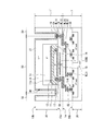
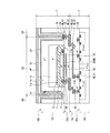
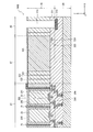
- FIG. 1 is a cross-sectional view schematically showing a configuration example of the image pickup apparatus according to the first embodiment of the present disclosure.
- FIG. 2 shows the thickness H of the P-type amorphous silicon carbide (a-SiC) film used for the anode electrode in the sensor substrate according to the first embodiment of the present disclosure, and the reflection of infrared rays on the incident surface side of the sensor substrate. It is a graph which shows the result of simulating the relationship with the rate.
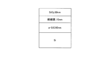
- FIG. 3 is a diagram showing a configuration on the incident surface side of the sensor substrate, which is set when the simulation of FIG. 2 is performed.
- FIG. 4 is a graph showing the result of simulating the relationship between the wavelength of the incident light and the transmittance of the incident light to the Si substrate in the sensor substrate according to the first embodiment of the present disclosure.
- FIG. 5 is a diagram showing a configuration on the incident surface side of the sensor substrate, which is set when the simulation of FIG. 4 is performed.
- FIG. 6A is a schematic cross-sectional view showing the manufacturing method of the image pickup apparatus according to the first embodiment of the present disclosure in the order of processes.
- FIG. 6B is a schematic cross-sectional view showing the manufacturing method of the image pickup apparatus according to the first embodiment of the present disclosure in the order of processes.
- FIG. 6C is a schematic cross-sectional view showing the manufacturing method of the image pickup apparatus according to the first embodiment of the present disclosure in the order of processes.
- FIG. 6D is a schematic cross-sectional view showing the manufacturing method of the image pickup apparatus according to the first embodiment of the present disclosure in the order of processes.
- FIG. 6E is a schematic cross-sectional view showing the manufacturing method of the image pickup apparatus according to the first embodiment of the present disclosure in the order of processes.
- FIG. 6F is a schematic cross-sectional view showing the manufacturing method of the image pickup apparatus according to the first embodiment of the present disclosure in the order of processes.
- FIG. 6G is a schematic cross-sectional view showing the manufacturing method of the image pickup apparatus according to the first embodiment of the present disclosure in the order of processes.
- FIG. 6G is a schematic cross-sectional view showing the manufacturing method of the image pickup apparatus according to the first embodiment of the present disclosure in the order of processes.
- FIG. 7 is a cross-sectional view schematically showing the configuration of the sensor substrate according to the modified example of the first embodiment of the present disclosure.
- FIG. 8 is a cross-sectional view schematically showing a configuration example of the sensor substrate according to the second embodiment of the present disclosure.
- FIG. 9 is a plan view schematically showing a configuration example of the image pickup apparatus according to the second embodiment of the present disclosure.
- FIG. 10 is a cross-sectional view showing a configuration example of the image pickup apparatus according to the second embodiment of the present disclosure.
- FIG. 11 is a block diagram showing a configuration example of the distance measuring device according to the third embodiment of the present disclosure.
- FIG. 12 is a diagram showing an example of a schematic configuration of an endoscopic surgery system.
- FIG. 12 is a diagram showing an example of a schematic configuration of an endoscopic surgery system.
- FIG. 13 is a block diagram showing an example of the functional configuration of the camera head and the CCU.
- FIG. 14 is a block diagram showing an example of a schematic configuration of a vehicle control system.
- FIG. 15 is an explanatory diagram showing an example of the installation positions of the vehicle exterior information detection unit and the image pickup unit.
- the direction may be explained using the words in the X-axis direction, the Y-axis direction, and the Z-axis direction.
- the X-axis direction and the Y-axis direction are directions parallel to the back surface 10b of the semiconductor substrate 10.
- the Z-axis direction is a direction perpendicularly intersecting the back surface 10b of the semiconductor substrate 10.
- the Z-axis direction is the thickness direction of the semiconductor substrate 10 and is also the thickness direction of the sensor substrate 1 including the semiconductor substrate 10.
- the X-axis direction, the Y-axis direction, and the Z-axis direction are orthogonal to each other.
- + or- may be added for P and N indicating the conductive type of the semiconductor.
- the semiconductor region marked with + or-me ans that the impurity concentration is relatively high or low, respectively, as compared with the semiconductor region not marked with + or-.
- the semiconductor regions have the same P and P (or N and N), it does not mean that the impurity concentrations of the respective semiconductor regions are exactly the same.
- FIG. 1 is a cross-sectional view schematically showing a configuration example of the image pickup apparatus 100 according to the first embodiment of the present disclosure.
- the image pickup device 100 shown in FIG. 1 is, for example, a back-illuminated solid-state image pickup device.
- the image pickup apparatus 100 includes a sensor substrate 1 and a logic substrate 3 joined to the surface 1a (lower surface in FIG. 1) side of the sensor substrate 1.
- the light to be detected by the sensor substrate 1 is, for example, infrared rays, and its wavelength band is 900 nm or more and 1100 nm or less.
- the sensor substrate 1 includes a semiconductor substrate 10, a plurality of pixels 50 provided on the semiconductor substrate 10, a light-shielding electrode 70 provided on the semiconductor substrate 10 (an example of the “light-shielding pixel separation unit” of the present disclosure), and the semiconductor substrate 10. It has a microlens 80 (an example of the "lens body” of the present disclosure) provided on the back surface 10b (upper surface in FIG. 1) side of the semiconductor substrate 10.
- the plurality of pixels 50 are arranged side by side in a direction parallel to the back surface 10b of the semiconductor substrate 10 (for example, the X-axis direction and the Y-axis direction).
- the pixel 50 is, for example, an avalanche photodiode, for example, a SPAD (Single Photon Avalanche Diode).
- the light-shielding electrode 70 is arranged in a region between adjacent pixels among the plurality of pixels 50. The light-shielding electrode 70 shields light between one adjacent pixel 50 and the other pixel 50 and separates them.
- the semiconductor substrate 10 is, for example, a single crystal silicon (Si) substrate.
- the semiconductor substrate 10 may be a single crystal Si layer.
- the single crystal Si layer can be obtained, for example, by forming a Si layer on a single crystal support substrate (not shown) by an epitaxial growth method and separating the support substrate from the formed Si layer.
- the semiconductor substrate 10 includes an N-type first semiconductor region 11, a P-type second semiconductor region 12, a P - type third semiconductor region 13, a P - type fourth semiconductor region 14, and P.
- a ⁇ type fifth semiconductor region 15, a P + type sixth semiconductor region 16, an N + type seventh semiconductor region 17, and a P + type eighth semiconductor region 18 are provided.
- the P-type second semiconductor region 12 is arranged on one surface 11b (upper surface in FIG. 1) of the N-type first semiconductor region 11.
- the P-type second semiconductor region 12 is in contact with one surface 11b of the N-type first semiconductor region 11.
- the portion where the first semiconductor region 11 and the second semiconductor region 12 are in contact with each other is the PN junction of the SPAD.
- the P-type P in the second semiconductor region 12 on the - -type third semiconductor region 13 is arranged in, P - P on the third semiconductor region 13 of the mold - the fourth semiconductor region 14 of the mold is disposed.
- the P - type third semiconductor region 13 and the P - type fourth semiconductor region 14 are examples of the “light absorption region” of the present disclosure.
- the P - type third semiconductor region 13 is arranged so as to cover the N-type first semiconductor region 11 and the P-type second semiconductor region 12 from the light irradiation surface (for example, the back surface) side, and is the first semiconductor. It is in contact with the region 11 and the second semiconductor region 12, respectively.
- the P - type fourth semiconductor region 14 is arranged so as to cover the P- type third semiconductor region 13 from the light irradiation surface side, and is in contact with the third semiconductor region 13.
- the P - type fifth semiconductor region 15 and the P + -type sixth semiconductor region 16 are arranged on the other surface 11a (lower surface in FIG. 1) side of the first semiconductor region 11.
- the P - type fifth semiconductor region 15 is in contact with the other surface 11a of the N-type first semiconductor region 11.
- the P + type sixth semiconductor region 16 faces the surface 10a (lower surface in FIG. 1) of the semiconductor substrate 10.
- a fifth semiconductor region 15 is arranged between the first semiconductor region 11 and the sixth semiconductor region 16.
- the N + type seventh semiconductor region 17 is provided on the other surface 11a side of the first semiconductor region 11 and faces the surface 10a (lower surface in FIG. 1) of the semiconductor substrate 10.
- the P-type impurity concentration in the above is as indicated by the appendix of + or-as described above. That is, the concentration of N-type impurities is higher in the N + -type seventh semiconductor region 17 than in the N-type first semiconductor region 11.
- the P-type second semiconductor region of the P - -type third towards the semiconductor region 13 is lower P-type impurity concentration of, P - than the third semiconductor region 13 of the type P - -type fourth semiconductor region 14
- the P-type impurity concentration is lower.
- the P - type fourth semiconductor region 14 may be intrinsic (i-type). Further, the third semiconductor region 13 and the fourth semiconductor region 14 may be composed of one semiconductor region in which the conductive type is P-type or P-type. That is, the "light absorption region" of the present disclosure may be composed of one semiconductor region in which the conductive type is P-type or P-type.
- the sensor substrate 1 includes an anode electrode 21, a first insulating film 23 (an example of the "insulating film” of the present disclosure) provided on the opposite side of the light absorption region with the anode electrode 21 interposed therebetween, and a second insulating film. It has 25 and.
- a trench H1 is formed from the back surface 10b to the front surface 10a in the region between adjacent pixels.
- the anode electrode 21 is continuously provided on the back surface 10b of the semiconductor substrate 10 and the inner side surface and the bottom surface of the trench H1.
- the anode electrode 21 has a first portion 211 arranged on the back surface 10b of the semiconductor substrate 10 and a second portion 212 arranged in the trench H1.
- the first portion 211 is in contact with the P - type fourth semiconductor region 14 in the Z-axis direction.
- the second portion 212 faces the second semiconductor region 12 in the X-axis direction and the Y-axis direction intersecting (for example, orthogonal to each other) in the Z-axis direction, and is in contact with the P - type fourth semiconductor region 14.
- the second portion 212 is in contact with the P ⁇ ⁇ type fourth semiconductor region 14 on the inner surface of the trench H1 and in contact with the P + type eighth semiconductor region 18 on the bottom surface of the trench H1.
- the anode electrode 21 is made of a P-type semiconductor having a refractive index of 1.8 or more and an optical bandgap of 1.9 eV or more.
- P-type semiconductors P-type amorphous silicon carbide (a-SiC), P-type polysilicon carbide (poly-SiC), P-type amorphous silicon nitride (a-SiN) or P-type polysilicon Nitride (poly-SiN) is exemplified.
- boron (B) is exemplified as the P-type impurity contained in the anode electrode 21, boron (B) is exemplified.
- the boron concentration in the anode electrode 21 is preferably 1 ⁇ 10 18 cm -3 or more.
- the anode electrode 21 is composed of a P-type semiconductor, it also functions as a hole storage layer.
- the hole storage layer can eliminate the electrons existing at the interface between the hole storage layer and another layer (for example, the fourth semiconductor region 14 or the first insulating film 23) by recombination, and exists at this interface. The dark current caused by electrons can be suppressed.
- the first insulating film 23 is continuously provided on the back surface 10b of the semiconductor substrate 10 and the inner and bottom surfaces of the trench H1 so as to cover the anode electrode 21.
- the first insulating film 23 is in contact with the anode electrode 21.
- the light-shielding electrode 70 is arranged in the trench H1 covered with the anode electrode 21 and the first insulating film 23, and is in contact with the first insulating film 23.
- the light-shielding electrode 70 is connected to, for example, a wiring having the same potential as the anode electrode 21.
- the second insulating film 25 is provided on the back surface 10b side of the semiconductor substrate 10 and covers the first insulating film 23 and the light-shielding electrode 70.
- the microlens 80 is provided on the opposite side of the light absorption region with the first insulating film 23 interposed therebetween in the thickness direction of the light absorption region (for example, the Z-axis direction).
- the microlens 80 is provided on the second insulating film 25.
- the side on which the microlens 80 is provided is the light incident surface side.
- the first insulating film 23 is a P-type semiconductor (for example, a P-type a-SiC film, a P-type poly-SiC film, a P-type a-SiN film, or a P-type poly-) constituting the anode electrode 21. It is preferably made of a material having a refractive index smaller than that of the SiN film).
- the first insulating film 23 is composed of an aluminum oxide film (Al 2 O 3 film), a silicon oxide film (SiO 2 film), or a hafnium oxide film (HfO 2 film).
- the magnitude relationship of the refractive index is defined between the first insulating film 23 and the anode electrode 21, so that the incident light on the sensor substrate 1 is the interface between the first insulating film 23 and the anode electrode 21. It is possible to suppress the reflection with.
- the first insulating film 23 When the first insulating film 23 is composed of an Al 2 O 3 film or an HfO 2 film, the first insulating film 23 also functions as a negative fixed charge film.
- the negative fixed charge film can trap the electrons present at the interface between the negative fixed charge film and another layer (for example, the anode electrode 21 or the second insulating film), and the electrons present at this interface can be trapped. The resulting dark current can be suppressed. Since the Al 2 O 3 film and the HfO 2 film have a stronger function as a negative fixed charge film than the SiO 2 film, it is better to use the Al 2 O 3 film or the HfO 2 film for the first insulating film 23. preferable. Thereby, the hole accumulation layer function of the anode electrode 21 can be further reinforced.
- the second insulating film 25 is preferably made of a material having the same refractive index as the first insulating film 23 or a material having a refractive index smaller than that of the first insulating film 23.
- the second insulating film 25 is composed of a SiO 2 film.
- Each of the plurality of pixels 50 includes an N-type first semiconductor region 11, a P-type second semiconductor region 12, a P - type third semiconductor region 13, and a P - type fourth semiconductor region 14. , P - type 5th semiconductor region 15, P + type 6th semiconductor region 16, N + type 7th semiconductor region 17, P + type 8th semiconductor region 18, and anode electrode 21.
- the first insulating film 23, the second insulating film 25, and the microlens 80 are arranged.
- the P - type third semiconductor region 13 and the P - type (or i-type) fourth semiconductor region 14 function as a light absorption region (photoelectric conversion region) of the SPAD.
- the P + type sixth semiconductor region 16 functions as a region for ohmic contacting the P-type fifth semiconductor region 15 to the contact electrode CGND described later.
- the P + type eighth semiconductor region 18 functions as a region for ohmic contacting the anode electrode 21 to the contact electrode CA described later.
- the N-type first semiconductor region 11 functions as a cathode.
- the N + type seventh semiconductor region 17 functions as a region for ohmic contacting the N-type first semiconductor region 11 to the contact electrode CK described later.
- the voltage for electron amplification is, for example, a voltage higher than the breakdown voltage of the PN junction between the N-type first semiconductor region 11 and the P-type second semiconductor region 12.
- the sensor substrate 1 can detect, for example, one photon for each pixel 50.
- the sensor substrate 1 includes contact electrodes CA, CK, and CGND provided on the surface 10a side of the semiconductor substrate 10, a plurality of wiring layers ML11 and ML12, and an interlayer insulating film 19 covering the surface 10a of the semiconductor substrate 10.
- One end of the contact electrode CA is in contact with the anode electrode 21, and the other end is in contact with the wiring layer ML11 having a first potential (for example, a negative potential).
- One end of the contact electrode CK is in contact with the seventh semiconductor region 17, and the other end is in contact with the wiring layer ML11 having a second potential (for example, a positive potential) having a potential higher than the first potential.
- the contact electrode CGND is in contact with the sixth semiconductor region 16, and the other end is in contact with the wiring layer ML11 having a reference potential (for example, ground potential (0V)).
- the contact electrodes CA, CK, and CGND are made of a metal such as aluminum (Al) or tungsten (W), for example.
- the wiring layers ML11 and ML12 are made of, for example, a metal such as copper (Cu).
- the logic substrate 3 includes a semiconductor substrate 30, an N-channel type MOS transistor TrN provided on the surface 30a (upper surface in FIG. 1) side of the semiconductor substrate 30, and a P channel provided on the surface 30a side of the semiconductor substrate 30.
- the interlayer insulating film 39 that covers the surface 30a of the above is provided.
- the logic substrate 3 has an insulating separation layer provided on the semiconductor substrate 30. The insulation separation layer electrically separates an element such as a MOS transistor TrN from another element.
- a bias circuit that applies a voltage between the first semiconductor region 11 (cathode) of the MOSFET and the anode electrode 21 by means of MOS transistors TrN, TrP, wiring layers ML31, ML32, ML33, etc. provided on the logic substrate 3.
- An arithmetic circuit or the like that performs arithmetic processing based on the signal output from the MOSFET is configured.
- the wiring layer ML12 located on the outermost surface side is exposed from the interlayer insulating film 19.
- the wiring layer ML 33 located on the outermost surface side is exposed from the interlayer insulating film 39.
- the wiring layers ML12 and ML33 may be referred to as pad electrodes, respectively.
- the wiring layers ML12 and ML33 are provided at positions facing each other in the Z-axis direction, and are joined to each other (for example, Cu—Cu joining). As a result, the sensor board 1 and the logic board 3 are joined to each other and integrated, and signals can be transmitted and received and a bias can be applied between the sensor board 1 and the logic board 3.
- FIG. 2 shows the thickness H of the P-type amorphous silicon carbide (a-SiC) film used for the anode electrode 21 and the incident surface side of the sensor substrate 1 in the sensor substrate 1 according to the first embodiment of the present disclosure. It is a graph which shows the result of simulating the relationship with the reflectance of infrared rays.
- the horizontal axis of FIG. 2 shows the film thickness H of the P-type a—SiC film, and the vertical axis shows the reflectance (%).
- FIG. 3 is a diagram showing a configuration on the incident surface side of the sensor substrate 1 set when performing the simulation of FIG. 2. As shown in FIG.
- the thickness of the P-type a-SiC film used for the anode electrode 21 is preferably 50 nm or more and 130 nm or less. It is more preferably 70 nm or more and 110 nm or less, and further preferably about 90 nm.
- the film thickness of the P-type a-SiC film used for the anode electrode 21 is within the above range, the reflectance of infrared rays on the incident surface side of the sensor substrate 1 can be suppressed to a low level.
- FIG. 4 is a graph showing the result of simulating the relationship between the wavelength of the incident light and the transmittance of the incident light to the Si substrate in the sensor substrate 1 according to the first embodiment of the present disclosure.
- the horizontal axis of FIG. 4 indicates the wavelength of the incident light, and the vertical axis indicates the transmittance (%) to the Si substrate.
- FIG. 5 is a diagram showing a configuration on the incident surface side of the sensor substrate 1 set when performing the simulation of FIG. 4. As shown in FIG. 5, in this simulation, a P-type a-SiC film (thickness: 90 nm), an insulating film (thickness: 15 nm), and a SiO 2 film (thickness: 50 nm) are formed on a Si substrate.
- the transmittance of the incident light on the Si substrate is 96% or more. It can be said that the a—SiC film, the insulating film and the SiO 2 film covering the Si substrate have high transmittance for the incident light having the above wavelengths. Further, regarding the insulating film between the a-SiC film and the SiO 2 film, the transmittance is slightly higher when the film type is the Al 2 O 3 film than when the film type is the SiO 2 film. This difference in transmittance is almost zero when the wavelength of the incident light is 900 nm, and becomes slightly higher when the wavelength of the incident light is larger than 900 nm. The difference in transmittance is slight.
- the image pickup apparatus 100 includes a film forming apparatus (including a CVD apparatus, a thermal oxidation furnace, a sputtering apparatus, and a resist coating apparatus), an exposure apparatus, an ion implantation apparatus, an annealing apparatus, an etching apparatus, a CMP (Chemical Mechanical Polishing) apparatus, and a bonding apparatus. It is manufactured using various devices such as. Hereinafter, these devices are collectively referred to as manufacturing devices.
- FIG. 6A to 6G are schematic cross-sectional views showing the manufacturing method of the image pickup apparatus 100 according to the first embodiment of the present disclosure in the order of processes.
- the manufacturing apparatus uses a CMOS process to separately manufacture the sensor substrate 1'and the logic substrate 3.
- P-type impurities and N-type impurities are sequentially ion-injected into the semiconductor substrate 10 from the surface 10a side of the semiconductor substrate 10 to perform thermal diffusion, and the semiconductor substrate 10 is subjected to the N-type first semiconductor region. 11, P-type second semiconductor region 12, P - type third semiconductor region 13, P - type fourth semiconductor region 14, P - type fifth semiconductor region 15, and P + type.
- the manufacturing apparatus forms the contact electrodes CA, CK, and CGND, the plurality of wiring layers ML11 and ML12, and the interlayer insulating film 19.
- the interlayer insulating film 19 is formed in a plurality of times so as to intervene between the wiring layers ML11 and ML12. As a result, the sensor substrate 1'is manufactured.
- the manufacturing apparatus forms an insulating separation layer (not shown), an N-channel type MOS transistor TrN, and a P-channel type MOS transistor TrP on the semiconductor substrate 30, and then a contact electrode CE and a plurality of wiring layers ML31. , ML32, ML33 and the interlayer insulating film 39 are formed.
- the interlayer insulating film 39 is formed by dividing it into a plurality of layers so as to intervene between the wiring layers ML31, ML32, and ML33. As a result, the logic substrate 3 is manufactured.
- the surface of the sensor substrate 1'and the surface of the logic substrate 3 are joined so as to face each other.
- the wiring layer M12 of the sensor substrate 1'and the wiring layer ML33 of the logic substrate 3 are Cu-Cu bonded, and the interlayer insulating film 19 of the sensor substrate 1'and the interlayer insulating film 39 of the logic substrate 3 are in close contact with each other. And are joined. As a result, the sensor board 1'and the logic board 3 are integrated.
- the manufacturing apparatus grinds the back surface 10b side of the semiconductor substrate 10 to set the thickness of the semiconductor substrate 10 to a preset value.
- the manufacturing apparatus forms the resist pattern RP1 on the back surface 10b (upper surface in FIG. 6B) of the semiconductor substrate 10.
- the resist pattern RP1 has a shape that opens on the region between the pixels 50 and covers the other regions.
- the manufacturing apparatus uses the resist pattern RP1 as a mask to etch the semiconductor substrate 10. This etching is performed by, for example, RIE (Reactive Ion Etching). As a result, the trench H1 is formed in the region between the pixels 50 on the semiconductor substrate 10. After that, the manufacturing apparatus removes the resist pattern RP1.
- the manufacturing apparatus forms the anode electrode 21 on the back surface 10b of the semiconductor substrate 10 by using a CVD method or the like.
- the anode electrode 21 is continuously formed on the back surface 10b of the semiconductor substrate 10 and the inner side surface and the bottom surface of the trench H1.
- the anode electrode 21 is, for example, a P-type a-SiC film, a P-type poly-SiC film, a P-type a-SiN film, or a P-type poly-SiN film, and the film thickness is 90 nm. ..
- the P-type a-SiC film or the P-type poly-SiC film is a plasma CVD method using silane (SiH 4 ), methane (CH 4 ), diborane (B 2 H 6 ), and hydrogen (H 2) as raw materials. Can be formed by.
- the P-type a-SiN film or the P-type poly-SiN film is a plasma CVD method using silane (SiH 4 ), ammonia (NH 3 ), diborane (B 2 H 6 ), and hydrogen (H 2) as raw materials.
- Diborane (B 2 H 6 ) is used as a doping gas for P-type impurities when forming an a-SiC film or an a-SiN film.
- the above conditions of gas flow rate, pressure, temperature, and RFPower are merely examples, and these values can be appropriately changed by the CVD apparatus.
- P-type a-SiC can be formed by a low temperature process of about 240 ° C. Therefore, when the anode electrode 21 is formed, the heat history loaded on the already formed N-type semiconductor region, P-type semiconductor region, and wiring layer can be suppressed to a small value, and the heat diffusion of impurities and the wiring layer can be suppressed. It is possible to suppress the melting of. This makes it possible to suppress fluctuations in the characteristics of the P-type semiconductor region, N-type semiconductor region, and wiring layer due to thermal history.
- the manufacturing apparatus uses a CVD method, a PVD method, or the like to form the first insulating film 23 on the back surface 10b side of the semiconductor substrate 10.
- the anode electrode 21 is covered with the first insulating film 23.
- the manufacturing apparatus uses a CVD method, a sputtering method, or the like to form a metal film 70'having a light-shielding property on the back surface 10b side of the semiconductor substrate 10 and embed the trench H1.
- the metal film 70' is, for example, tungsten (W).
- the manufacturing apparatus forms the resist pattern RP2 on the metal film 70'.
- the resist pattern RP2 has a shape that covers, for example, a region between adjacent pixels 50 and exposes the other regions.
- the manufacturing apparatus uses the resist pattern RP2 as a mask to etch the metal film 70'. As a result, as shown in FIG. 6G, the light-shielding electrode 70 is formed from the metal film 70'. After that, the manufacturing apparatus removes the resist pattern RP2.
- the manufacturing apparatus uses a CVD method, a PVD method, or the like to form the second insulating film 25 on the back surface 10b side of the semiconductor substrate 10.
- the thickness of the second insulating film 25 is, for example, 50 nm.
- the manufacturing apparatus mounts the microlens 80 (see FIG. 1) on the second insulating film 25. Through the above steps, the image pickup apparatus 100 shown in FIG. 1 is completed.
- the image pickup apparatus 100 includes an N-type first semiconductor region 11 and a P-type second semiconductor region 12 in contact with one surface 11b of the first semiconductor region 11. , A light absorption region (third semiconductor region 13 and a fourth semiconductor region 14) provided on the opposite side of the first semiconductor region 11 with the second semiconductor region 12 interposed therebetween, and a second semiconductor region 12 with the light absorption region interposed therebetween. It is provided with an anode electrode 21 provided at a position facing the surface.
- the anode electrode 21 is made of a P-type semiconductor having a refractive index of 1.8 or more and an optical bandgap of 1.9 eV or more.
- the P-type semiconductor for example, P-type amorphous silicon carbide (a-SiC), P-type polysilicon carbide (poly-SiC), P-type amorphous silicon nitride (a-SiN) or P-type.
- Polysilicon nitride (poly-SiN) can be used. Since these films can be formed by the CVD (Chemical Vapor Deposition) method while doping P-type impurities such as boron (B) in situ, the concentration of P-type impurities in the film can be made uniform or almost uniform. It is possible to homogenize the composition of the film and the crystal structure easily.
- the image pickup apparatus 100 can suppress variations in the electrical resistance (for example, resistivity) of the anode electrode 21, so that the characteristics deteriorate due to the variations (for example, the sensitivity varies among a plurality of pixels). What happens) can be suppressed.
- the electrical resistance for example, resistivity
- P-type poly-SiC, P-type a-SiN, or P-type poly-SiN are also wide-gap materials and hardly absorb infrared rays. Therefore, it is possible to thicken the light absorption region. The thicker the light absorption region, the higher the photoelectric conversion efficiency of the pixel 50, so that the sensitivity of the pixel 50 can be improved.
- the electrode width of the second portion 212 of the anode electrode 21 is narrower and deeper in the Z-axis direction than in the case of performing multi-stage ion implantation at high acceleration. Is easy. Since it is easy to form the anode electrode 21 deeply in the Z-axis direction, the light absorption region of the semiconductor substrate 10 can be thickened. As described above, the thicker the light absorption region, the higher the photoelectric conversion efficiency of the pixel 50, so that the sensitivity of the pixel 50 can be further improved.
- P-type impurities such as boron (B) contained in the anode electrode 21 are doped in situ at the time of film formation.
- the annealing step for activating the P-type impurity is not required as compared with the case of ion-implanting the P-type impurity, so that the number of manufacturing steps can be reduced and simplified.
- the anode electrode 21 is formed in the back surface processing step after forming the ML33 from the wiring layers ML11, ML12, and ML31 and bonding the semiconductor substrates 10 and 30 to each other as described above.
- the heat history when forming the N-type semiconductor region and the P-type semiconductor region, the heat history when forming the ML33 from the wiring layers ML11, ML12, and ML31, and the heat history when joining the semiconductor substrates 10 and 30 are as follows. It is not loaded on the anode electrode 21. As a result, it is possible to suppress fluctuations in the characteristics of the anode electrode 21 due to thermal history.
- FIG. 7 is a cross-sectional view schematically showing the configuration of the sensor substrate 1A according to the modified example of the first embodiment of the present disclosure.
- the sensor substrate 1A has a color filter CF between the second insulating film 25 and the microlens 80.
- the color filter CF includes, for example, a red filter CF-R, a green filter CF-G, and a blue filter CF-B.
- One of the red filter CF-R, the green filter CF-G, and the blue filter CF-B is arranged in each of the plurality of pixels 50.
- P-type a-SiC, P-type poly-SiC, P-type a-SiN, or P-type poly-SiN can be used as the anode electrode 21.
- These can be formed by a CVD method, and the concentration of P-type impurities in the film can be made uniform or substantially uniform.
- the image pickup apparatus provided with the sensor substrate 1A has the same effect as that of the first embodiment. Further, since the sensor substrate 1A has the color filter CF, the image pickup apparatus provided with the sensor substrate 1A can output a color image signal.
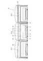
- FIG. 8 is a cross-sectional view schematically showing a configuration example of the sensor substrate 1B according to the second embodiment of the present disclosure.
- the sensor substrate 1B shown in FIG. 8 has a plurality of pixels 250.
- Each of the plurality of pixels 250 is, for example, an avalanche photodiode.
- the pixel 250 includes an N-type first semiconductor region 201, a P-type second semiconductor region 202 provided below the N-type first semiconductor region 201, and a well layer 203. Have.
- the N-type first semiconductor region 201 and the P-type second semiconductor region 202 are provided in the well 203 layer.
- the well layer 203 may be a P-type semiconductor region. Further, the well layer 203 may be, for example, a low-concentration semiconductor region in which the P-type impurity concentration is less than 1 ⁇ 10 15 cm -3. This makes it easier to deplete the well layer 203, and it is possible to improve the detection efficiency called PDE (Photon Detection Efficiency).
- PDE Photon Detection Efficiency
- the N-type first semiconductor region 201 is made of, for example, N-type Si (silicon).
- the P-type second semiconductor region 202 is made of, for example, P-type Si (silicon).
- the portion where the N-type first semiconductor region 201 and the P-type second semiconductor region 202 are in contact with each other is the PN junction of the avalanche photodiode.
- the carriers generated by the incident light on the sensor substrate 1B are avalanche amplified at the above-mentioned PN junction.
- the P-type second semiconductor region 202 is preferably depleted, which can improve PDE.
- the N-type first semiconductor region 201 functions as a cathode, for example, and is connected to a circuit via a contact electrode 204.
- the anode electrode 205 is continuous between the N-type first semiconductor region 201 and the separation region 208, between the well layer 203 and the separation region 208, and the lower part of the well layer 203 (the back surface side of the pixel 250). It is provided.
- the anode electrode 205 is connected to the bias circuit via the contact electrode 206.
- the anode electrode 205 is the same as the anode electrode 21 described in the first embodiment, for example, a P-type amorphous silicon carbide (a-SiC), a P-type polysilicon carbide (poly-SiC), and a P-type amorphous silicon knight. It is composed of a ride (a-SiN) or a P-type polysilicon nitride (poly-SiN).
- the sensor substrate 1B may be applied to a back-illuminated image pickup device or a front-illuminated image pickup device.
- a lens body such as a microlens is placed in the lower part of the well layer 203 (the side opposite to the side on which the N-type first semiconductor region 201 is formed). It is laminated.
- the logic substrate 3B (FIG. 10 described later) is located on the upper surface side of the well layer 203 (the surface on which the N-type first semiconductor region 201 is formed).
- a lens body such as a microlens is laminated via (see) and the like.
- the separation region 208 is a region for separating adjacent pixels 250 from each other, and is composed of, for example, a silicon oxide film.
- the separation region 208 may be formed so as to penetrate from the upper surface side to the lower surface side of the well layer 203 as shown in FIG. 8, or may penetrate only a part of the well layer 203 from the upper surface side to the lower surface side. It may be formed.
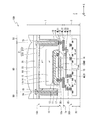
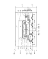
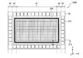
- FIG. 9 is a plan view schematically showing a configuration example of the image pickup apparatus 100B according to the second embodiment of the present disclosure.
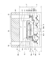
- FIG. 10 is a cross-sectional view showing a configuration example of the image pickup apparatus 100B according to the second embodiment of the present disclosure.
- FIG. 10 shows a cross section of the plan view shown in FIG. 9 cut along the line X9-X'9.
- the plurality of pixels 250 are arranged in an array in the pixel region A1 provided on the sensor substrate 1B.
- the logic board 3B is connected to the lower surface of the sensor board 1B (the surface opposite to the light incident surface) on which the plurality of pixels 250 are arranged.
- the logic board 3B is formed with a circuit that processes a signal from the pixel 250 and supplies electric power to the pixel 250.
- a peripheral region A2 is arranged outside the pixel region A1. Further, a pad region A3 is arranged outside the peripheral region A2. As shown in FIG. 10, the pad region A3 is a vertical hole extending from the upper end of the sensor substrate 1B to the inside of the wiring layer 311 and has a pad opening 313 which is a hole for wiring to the electrode pad 312. It is formed so as to line up in a straight line.
- An electrode pad 312 for wiring is provided at the bottom of the pad opening 313.
- the electrode pad 312 is used, for example, when it is connected to the wiring in the wiring layer 311 or when it is connected to another external device (chip or the like). Further, the wiring layer close to the bonding surface between the sensor substrate 1B and the logic substrate 3B may also serve as the electrode pad 312.
- the wiring layer 311 formed on the sensor substrate 1B and the wiring layer formed on the logic substrate 3B are formed to include an insulating film and a plurality of wirings, respectively, and the plurality of wirings and the electrode pad 312 are formed of, for example, copper (Cu). It is made of a metal such as aluminum (Al) or aluminum (Al).
- the wiring formed in the pixel region A1 and the peripheral region A2 is also formed of the same material.
- a peripheral region A2 is provided between the pixel region A1 and the pad region A3.
- the peripheral region A2 has a ring-shaped N-type semiconductor region 321 that surrounds the pixel region A1 in a plan view, and a ring-shaped P-type semiconductor region 322 that surrounds the pixel region A1 in a plan view outside the N-type semiconductor region 321. ..
- the outer peripheral side surface of the N-type semiconductor region 321 is in contact with the inner peripheral side surface of the P-type semiconductor region 322.
- the P-type semiconductor region 322 is connected to the wiring layer 324 via the contact electrode 325, and the wiring layer 324 is connected to the ground (GND).
- two trenches 323 are formed in the N-type semiconductor region 321. These trenches 323 are provided to physically separate the pixel region A1 and the peripheral region A2.
- FIG. 10 shows a case where two trenches 323 are formed, but the number of trenches 323 formed may be one or three or more.
- a high voltage is applied between the first semiconductor region 201 (cathode) and the anode electrode 205 in the plurality of pixels 250. Further, the peripheral region A2 is grounded to GND. In the separated region between the pixel region A1 and the peripheral region A2, a high electric field region is generated due to a high voltage applied to the anode electrode 205, and breakdown may occur. In order to avoid breakdown, it is conceivable to widen the separation region between the pixel region A1 and the peripheral region A2, but widening the separation region makes the sensor substrate 1B large.
- a trench 323 is formed in order to suppress the occurrence of breakdown in the separation region between the pixel region A1 and the peripheral region A2.
- the trench 323 makes it possible to suppress breakdown without widening the separation region.
- the sensor substrate 1B includes an N-type first semiconductor region 201 and a P-type second semiconductor region 202 in contact with one surface of the first semiconductor region 201.
- the well layer 203 (an example of the "light absorption region" of the present disclosure) provided on the opposite side of the first semiconductor region 201 across the second semiconductor region 202 faces the second semiconductor region 12 with the well layer 203 interposed therebetween.
- the anode electrode 205 provided at the position is provided.
- the anode electrode 205 is a P-type semiconductor having a refractive index of 1.8 or more and an optical bandgap of 1.9 eV or more (for example, P-type a-SiC, P-type poly-SiC, P-type a-). It is composed of SiN or P-type poly-SiN).
- the anode electrode 205 can be formed by the CVD method, and the concentration of P-type impurities in the film can be made uniform or almost uniform.
- the image pickup apparatus provided with the sensor substrate 1B has the same effect as that of the first embodiment.
- FIGS. 10 and 11 The configurations of the peripheral region A2 and the pad region A3 shown in FIGS. 10 and 11 are also applicable to the first embodiment.
- pixel 250 may be replaced with pixel 50 shown in FIG. 1 or FIG.
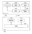
- FIG. 11 is a block diagram showing a configuration example of the distance measuring device 200 according to the third embodiment of the present disclosure.
- the distance measuring device 200 (an example of the “electronic device” of the present disclosure) includes a distance image sensor 401 and a light source device 411 (an example of the “light source” of the present disclosure).
- the light source device 411 emits light (for example, infrared rays) in a preset wavelength band.
- the distance image sensor 401 includes an optical system 402, a sensor chip 403, an image processing circuit 404, a monitor 405, and a memory 406. Then, the distance image sensor 401 is projected from the light source device 411 toward the subject 420 and receives the light (modulated light or pulsed light) reflected on the surface of the subject 420 according to the distance to the subject 420. It is possible to acquire a distance image.
- the optical system 402 is configured to have one or a plurality of lenses, and guides the image light (incident light) from the subject 420 to the sensor chip 403 and forms an image on the light receiving surface (sensor unit) of the sensor chip 403. ..
- the sensor chip 403 photoelectrically converts infrared rays and outputs a signal. For example, a light receiving signal (APD OUT) is output from the sensor chip 403. A distance signal indicating a distance obtained from the output received light signal is supplied to the image processing circuit 404. As the sensor chip 403, the image pickup device 100 of the first embodiment or the image pickup device 100B of the second embodiment described above is applied.
- the image processing circuit 404 performs image processing for constructing a distance image based on the distance signal supplied from the sensor chip 403, and the distance image (image data) obtained by the image processing is supplied to the monitor 405 and displayed. Or it is supplied to the memory 406 and stored (recorded).
- the distance image sensor 401 configured in this way, the characteristics of imaging can be improved by applying the above-mentioned imaging devices 100 and 100B, and for example, a more accurate distance image can be acquired.
- the light to be detected is not limited to infrared rays.
- the light to be detected may be, for example, visible light having a wavelength band of 400 nm or more and 650 nm or less.
- the present technology includes various embodiments not described here. At least one of the various omissions, substitutions and modifications of the components may be made without departing from the gist of the embodiments and modifications described above. Further, the effects described in the present specification are merely exemplary and not limited, and other effects may be obtained.
- the technology according to the present disclosure (the present technology) can be applied to various products.
- the techniques according to the present disclosure may be applied to an endoscopic surgery system.
- FIG. 12 is a diagram showing an example of a schematic configuration of an endoscopic surgery system to which the technique according to the present disclosure (the present technique) can be applied.
- FIG. 12 illustrates how the surgeon (doctor) 11131 is performing surgery on patient 11132 on patient bed 11133 using the endoscopic surgery system 11000.
- the endoscopic surgery system 11000 includes an endoscope 11100, other surgical tools 11110 such as an abdominal tube 11111 and an energy treatment tool 11112, and a support arm device 11120 that supports the endoscope 11100.
- a cart 11200 equipped with various devices for endoscopic surgery.
- the endoscope 11100 is composed of a lens barrel 11101 in which a region having a predetermined length from the tip is inserted into the body cavity of the patient 11132, and a camera head 11102 connected to the base end of the lens barrel 11101.
- the endoscope 11100 configured as a so-called rigid mirror having a rigid barrel 11101 is illustrated, but the endoscope 11100 may be configured as a so-called flexible mirror having a flexible barrel. good.
- An opening in which an objective lens is fitted is provided at the tip of the lens barrel 11101.
- a light source device 11203 is connected to the endoscope 11100, and the light generated by the light source device 11203 is guided to the tip of the lens barrel by a light guide extending inside the lens barrel 11101, and is an objective. It is irradiated toward the observation target in the body cavity of the patient 11132 through the lens.
- the endoscope 11100 may be a direct endoscope, a perspective mirror, or a side endoscope.
- An optical system and an image pickup element are provided inside the camera head 11102, and the reflected light (observation light) from the observation target is focused on the image pickup element by the optical system.
- the observation light is photoelectrically converted by the image pickup device, and an electric signal corresponding to the observation light, that is, an image signal corresponding to the observation image is generated.
- the image signal is transmitted as RAW data to the camera control unit (CCU: Camera Control Unit) 11201.
- the CCU11201 is composed of a CPU (Central Processing Unit), a GPU (Graphics Processing Unit), and the like, and comprehensively controls the operations of the endoscope 11100 and the display device 11202. Further, the CCU11201 receives an image signal from the camera head 11102, and performs various image processing on the image signal for displaying an image based on the image signal, such as development processing (demosaic processing).
- a CPU Central Processing Unit
- GPU Graphics Processing Unit
- the display device 11202 displays an image based on the image signal processed by the CCU 11201 under the control of the CCU 11201.
- the light source device 11203 is composed of, for example, a light source such as an LED (Light Emitting Diode), and supplies irradiation light for photographing an operating part or the like to the endoscope 11100.
- a light source such as an LED (Light Emitting Diode)
- LED Light Emitting Diode
- the input device 11204 is an input interface for the endoscopic surgery system 11000.
- the user can input various information and input instructions to the endoscopic surgery system 11000 via the input device 11204.
- the user inputs an instruction to change the imaging conditions (type of irradiation light, magnification, focal length, etc.) by the endoscope 11100.
- the treatment tool control device 11205 controls the drive of the energy treatment tool 11112 for cauterizing, incising, sealing a blood vessel, or the like.
- the pneumoperitoneum device 11206 uses a gas in the pneumoperitoneum tube 11111 to inflate the body cavity of the patient 11132 for the purpose of securing the field of view by the endoscope 11100 and securing the work space of the operator. Is sent.
- the recorder 11207 is a device capable of recording various information related to surgery.
- the printer 11208 is a device capable of printing various information related to surgery in various formats such as text, images, and graphs.
- the light source device 11203 that supplies the irradiation light to the endoscope 11100 when photographing the surgical site can be composed of, for example, an LED, a laser light source, or a white light source composed of a combination thereof.
- a white light source is configured by a combination of RGB laser light sources, the output intensity and output timing of each color (each wavelength) can be controlled with high accuracy. Therefore, the light source device 11203 adjusts the white balance of the captured image. It can be carried out.
- the laser light from each of the RGB laser light sources is irradiated to the observation target in a time-division manner, and the drive of the image sensor of the camera head 11102 is controlled in synchronization with the irradiation timing to correspond to each of RGB. It is also possible to capture the image in a time-division manner. According to this method, a color image can be obtained without providing a color filter in the image pickup device.
- the drive of the light source device 11203 may be controlled so as to change the intensity of the output light at predetermined time intervals.
- the drive of the image sensor of the camera head 11102 in synchronization with the timing of the change of the light intensity to acquire an image in time division and synthesizing the image, so-called high dynamic without blackout and overexposure. Range images can be generated.
- the light source device 11203 may be configured to be able to supply light in a predetermined wavelength band corresponding to special light observation.
- special light observation for example, by utilizing the wavelength dependence of light absorption in body tissue, the surface layer of the mucous membrane is irradiated with light in a narrower band than the irradiation light (that is, white light) during normal observation.
- a so-called narrow band light observation is performed in which a predetermined tissue such as a blood vessel is photographed with high contrast.
- fluorescence observation may be performed in which an image is obtained by fluorescence generated by irradiating with excitation light.
- the body tissue is irradiated with excitation light to observe the fluorescence from the body tissue (autofluorescence observation), or a reagent such as indocyanine green (ICG) is locally injected into the body tissue and the body tissue is injected. It is possible to obtain a fluorescence image by irradiating the excitation light corresponding to the fluorescence wavelength of the reagent.
- the light source device 11203 may be configured to be capable of supplying narrowband light and / or excitation light corresponding to such special light observation.
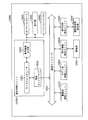
- FIG. 13 is a block diagram showing an example of the functional configuration of the camera head 11102 and CCU11201 shown in FIG.
- the camera head 11102 includes a lens unit 11401, an image pickup unit 11402, a drive unit 11403, a communication unit 11404, and a camera head control unit 11405.
- CCU11201 has a communication unit 11411, an image processing unit 11412, and a control unit 11413.
- the camera head 11102 and CCU11201 are communicably connected to each other by a transmission cable 11400.
- the lens unit 11401 is an optical system provided at a connection portion with the lens barrel 11101.
- the observation light taken in from the tip of the lens barrel 11101 is guided to the camera head 11102 and incident on the lens unit 11401.
- the lens unit 11401 is configured by combining a plurality of lenses including a zoom lens and a focus lens.
- the image pickup unit 11402 is composed of an image pickup element.
- the image pickup element constituting the image pickup unit 11402 may be one (so-called single plate type) or a plurality (so-called multi-plate type).
- each image pickup element may generate an image signal corresponding to each of RGB, and a color image may be obtained by synthesizing them.
- the image pickup unit 11402 may be configured to have a pair of image pickup elements for acquiring image signals for the right eye and the left eye corresponding to 3D (Dimensional) display, respectively.
- the 3D display enables the operator 11131 to more accurately grasp the depth of the living tissue in the surgical site.
- a plurality of lens units 11401 may be provided corresponding to each image pickup element.
- the image pickup unit 11402 does not necessarily have to be provided on the camera head 11102.
- the image pickup unit 11402 may be provided inside the lens barrel 11101 immediately after the objective lens.
- the drive unit 11403 is composed of an actuator, and the zoom lens and focus lens of the lens unit 11401 are moved by a predetermined distance along the optical axis under the control of the camera head control unit 11405. As a result, the magnification and focus of the image captured by the image pickup unit 11402 can be adjusted as appropriate.
- the communication unit 11404 is configured by a communication device for transmitting and receiving various information to and from the CCU11201.
- the communication unit 11404 transmits the image signal obtained from the image pickup unit 11402 as RAW data to the CCU 11201 via the transmission cable 11400.
- the communication unit 11404 receives a control signal for controlling the drive of the camera head 11102 from the CCU 11201 and supplies the control signal to the camera head control unit 11405.
- the control signal includes, for example, information to specify the frame rate of the captured image, information to specify the exposure value at the time of imaging, and / or information to specify the magnification and focus of the captured image. Contains information about the condition.
- the image pickup conditions such as the frame rate, exposure value, magnification, and focus may be appropriately specified by the user, or may be automatically set by the control unit 11413 of CCU11201 based on the acquired image signal. good.
- the endoscope 11100 is equipped with a so-called AE (Auto Exposure) function, an AF (Auto Focus) function, and an AWB (Auto White Balance) function.
- the camera head control unit 11405 controls the drive of the camera head 11102 based on the control signal from the CCU 11201 received via the communication unit 11404.
- the communication unit 11411 is configured by a communication device for transmitting and receiving various information to and from the camera head 11102.
- the communication unit 11411 receives an image signal transmitted from the camera head 11102 via the transmission cable 11400.
- the communication unit 11411 transmits a control signal for controlling the drive of the camera head 11102 to the camera head 11102.
- Image signals and control signals can be transmitted by telecommunications, optical communication, or the like.
- the image processing unit 11412 performs various image processing on the image signal which is the RAW data transmitted from the camera head 11102.
- the control unit 11413 performs various controls related to the imaging of the surgical site and the like by the endoscope 11100 and the display of the captured image obtained by the imaging of the surgical site and the like. For example, the control unit 11413 generates a control signal for controlling the drive of the camera head 11102.
- control unit 11413 causes the display device 11202 to display an image captured by the surgical unit or the like based on the image signal processed by the image processing unit 11412.
- the control unit 11413 may recognize various objects in the captured image by using various image recognition techniques.
- the control unit 11413 detects a surgical tool such as forceps, a specific biological part, bleeding, mist when using the energy treatment tool 11112, etc. by detecting the shape, color, etc. of the edge of the object included in the captured image. Can be recognized.
- the control unit 11413 may superimpose and display various surgical support information on the image of the surgical unit by using the recognition result. By superimposing and displaying the surgical support information and presenting it to the surgeon 11131, the burden on the surgeon 11131 can be reduced and the surgeon 11131 can surely proceed with the surgery.
- the transmission cable 11400 connecting the camera head 11102 and CCU11201 is an electric signal cable corresponding to electric signal communication, an optical fiber corresponding to optical communication, or a composite cable thereof.
- the communication is performed by wire using the transmission cable 11400, but the communication between the camera head 11102 and the CCU11201 may be performed wirelessly.
- the above is an example of an endoscopic surgery system to which the technology according to the present disclosure can be applied.
- the technique according to the present disclosure can be applied to, for example, the endoscope 11100, the camera head 11102 (imaging unit 11402), the CCU 11201 (image processing unit 11412), and the like, among the configurations described above.
- the image pickup device 100 shown in FIG. 1, the image pickup device 100B shown in FIG. 9, the sensor substrate 1 shown in FIG. 1, the sensor substrate 1A shown in FIG. 7, and the sensor substrate shown in FIG. 1B can be applied to the imaging unit 10402.
- the image pickup unit 11402 of the camera head 11102 By applying the technique according to the present disclosure to the endoscope 11100, the image pickup unit 11402 of the camera head 11102, the image processing unit 11412 of the CCU 11201, etc., for example, the variation in sensitivity among a plurality of pixels is reduced, and a clearer technique is performed. Since the part image can be obtained, the operator can surely confirm the part.
- the technique according to the present disclosure may be applied to other, for example, a microscopic surgery system.
- the technology according to the present disclosure can be applied to various products.
- the technology according to the present disclosure is realized as a device mounted on a moving body of any kind such as an automobile, an electric vehicle, a hybrid electric vehicle, a motorcycle, a bicycle, a personal mobility, an airplane, a drone, a ship, and a robot. You may.
- FIG. 14 is a block diagram showing a schematic configuration example of a vehicle control system, which is an example of a mobile control system to which the technique according to the present disclosure can be applied.
- the vehicle control system 12000 includes a plurality of electronic control units connected via the communication network 12001.
- the vehicle control system 12000 includes a drive system control unit 12010, a body system control unit 12020, an outside information detection unit 12030, an in-vehicle information detection unit 12040, and an integrated control unit 12050.
- a microcomputer 12051, an audio image output unit 12052, and an in-vehicle network I / F (interface) 12053 are shown as a functional configuration of the integrated control unit 12050.
- the drive system control unit 12010 controls the operation of the device related to the drive system of the vehicle according to various programs.
- the drive system control unit 12010 has a driving force generator for generating a driving force of a vehicle such as an internal combustion engine or a driving motor, a driving force transmission mechanism for transmitting the driving force to the wheels, and a steering angle of the vehicle. It functions as a control device such as a steering mechanism for adjusting and a braking device for generating braking force of the vehicle.
- the body system control unit 12020 controls the operation of various devices mounted on the vehicle body according to various programs.
- the body system control unit 12020 functions as a keyless entry system, a smart key system, a power window device, or a control device for various lamps such as headlamps, back lamps, brake lamps, turn signals or fog lamps.
- the body system control unit 12020 may be input with radio waves transmitted from a portable device that substitutes for the key or signals of various switches.
- the body system control unit 12020 receives inputs of these radio waves or signals and controls a vehicle door lock device, a power window device, a lamp, and the like.
- the outside information detection unit 12030 detects information outside the vehicle equipped with the vehicle control system 12000.
- the image pickup unit 12031 is connected to the vehicle outside information detection unit 12030.
- the vehicle outside information detection unit 12030 causes the image pickup unit 12031 to capture an image of the outside of the vehicle and receives the captured image.
- the out-of-vehicle information detection unit 12030 may perform object detection processing or distance detection processing such as a person, a vehicle, an obstacle, a sign, or a character on the road surface based on the received image.
- the image pickup unit 12031 is an optical sensor that receives light and outputs an electric signal according to the amount of the light received.
- the image pickup unit 12031 can output an electric signal as an image or can output it as distance measurement information. Further, the light received by the image pickup unit 12031 may be visible light or invisible light such as infrared light.
- the in-vehicle information detection unit 12040 detects the in-vehicle information.
- a driver state detection unit 12041 that detects the driver's state is connected to the in-vehicle information detection unit 12040.
- the driver state detection unit 12041 includes, for example, a camera that images the driver, and the in-vehicle information detection unit 12040 determines the degree of fatigue or concentration of the driver based on the detection information input from the driver state detection unit 12041. It may be calculated, or it may be determined whether the driver has fallen asleep.
- the microcomputer 12051 calculates the control target value of the driving force generator, the steering mechanism, or the braking device based on the information inside and outside the vehicle acquired by the vehicle exterior information detection unit 12030 or the vehicle interior information detection unit 12040, and the drive system control unit.
- a control command can be output to 12010.
- the microcomputer 12051 realizes ADAS (Advanced Driver Assistance System) functions including vehicle collision avoidance or impact mitigation, follow-up driving based on inter-vehicle distance, vehicle speed maintenance driving, vehicle collision warning, vehicle lane deviation warning, and the like. It is possible to perform cooperative control for the purpose of.
- ADAS Advanced Driver Assistance System
- the microcomputer 12051 controls the driving force generating device, the steering mechanism, the braking device, and the like based on the information around the vehicle acquired by the vehicle exterior information detection unit 12030 or the vehicle interior information detection unit 12040. It is possible to perform coordinated control for the purpose of automatic driving that runs autonomously without depending on the operation.
- the microcomputer 12051 can output a control command to the body system control unit 12020 based on the information outside the vehicle acquired by the vehicle outside information detection unit 12030.
- the microcomputer 12051 controls the headlamps according to the position of the preceding vehicle or the oncoming vehicle detected by the outside information detection unit 12030, and performs cooperative control for the purpose of anti-glare such as switching the high beam to the low beam. It can be carried out.
- the audio image output unit 12052 transmits an output signal of at least one of audio and image to an output device capable of visually or audibly notifying information to the passenger or the outside of the vehicle.
- an audio speaker 12061, a display unit 12062, and an instrument panel 12063 are exemplified as output devices.
- the display unit 12062 may include, for example, at least one of an onboard display and a head-up display.
- FIG. 15 is a diagram showing an example of the installation position of the image pickup unit 12031.
- the vehicle 12100 has an imaging unit 12101, 12102, 12103, 12104, 12105 as an imaging unit 12031.
- the image pickup units 12101, 12102, 12103, 12104, 12105 are provided, for example, at positions such as the front nose, side mirrors, rear bumpers, back doors, and the upper part of the windshield in the vehicle interior of the vehicle 12100.
- the image pickup unit 12101 provided in the front nose and the image pickup section 12105 provided in the upper part of the windshield in the vehicle interior mainly acquire an image in front of the vehicle 12100.
- the image pickup units 12102 and 12103 provided in the side mirror mainly acquire images of the side of the vehicle 12100.
- the image pickup unit 12104 provided in the rear bumper or the back door mainly acquires an image of the rear of the vehicle 12100.
- the images in front acquired by the image pickup units 12101 and 12105 are mainly used for detecting a preceding vehicle, a pedestrian, an obstacle, a traffic light, a traffic sign, a lane, or the like.
- FIG. 15 shows an example of the shooting range of the imaging units 12101 to 12104.
- the imaging range 12111 indicates the imaging range of the imaging unit 12101 provided on the front nose
- the imaging ranges 12112 and 12113 indicate the imaging range of the imaging units 12102 and 12103 provided on the side mirrors, respectively
- the imaging range 12114 indicates the imaging range.
- the imaging range of the imaging unit 12104 provided on the rear bumper or the back door is shown. For example, by superimposing the image data captured by the image pickup units 12101 to 12104, a bird's-eye view image of the vehicle 12100 can be obtained.
- At least one of the image pickup units 12101 to 12104 may have a function of acquiring distance information.
- at least one of the image pickup units 12101 to 12104 may be a stereo camera including a plurality of image pickup elements, or may be an image pickup element having pixels for phase difference detection.
- the microcomputer 12051 has a distance to each three-dimensional object in the image pickup range 12111 to 12114 based on the distance information obtained from the image pickup unit 12101 to 12104, and a temporal change of this distance (relative speed with respect to the vehicle 12100). By obtaining can. Further, the microcomputer 12051 can set an inter-vehicle distance to be secured in advance in front of the preceding vehicle, and can perform automatic brake control (including follow-up stop control), automatic acceleration control (including follow-up start control), and the like. In this way, it is possible to perform coordinated control for the purpose of automatic driving or the like in which the vehicle travels autonomously without depending on the operation of the driver.
- automatic brake control including follow-up stop control
- automatic acceleration control including follow-up start control
- the microcomputer 12051 converts three-dimensional object data related to a three-dimensional object into two-wheeled vehicles, ordinary vehicles, large vehicles, pedestrians, electric poles, and other three-dimensional objects based on the distance information obtained from the image pickup units 12101 to 12104. It can be classified and extracted and used for automatic avoidance of obstacles. For example, the microcomputer 12051 distinguishes obstacles around the vehicle 12100 into obstacles that are visible to the driver of the vehicle 12100 and obstacles that are difficult to see. Then, the microcomputer 12051 determines the collision risk indicating the risk of collision with each obstacle, and when the collision risk is equal to or higher than the set value and there is a possibility of collision, the microcomputer 12051 via the audio speaker 12061 or the display unit 12062. By outputting an alarm to the driver and performing forced deceleration and avoidance steering via the drive system control unit 12010, driving support for collision avoidance can be provided.
- At least one of the image pickup units 12101 to 12104 may be an infrared camera that detects infrared rays.
- the microcomputer 12051 can recognize a pedestrian by determining whether or not a pedestrian is present in the captured image of the imaging unit 12101 to 12104.
- pedestrian recognition is, for example, a procedure for extracting feature points in an image captured by an image pickup unit 12101 to 12104 as an infrared camera, and pattern matching processing is performed on a series of feature points indicating the outline of an object to determine whether or not the pedestrian is a pedestrian. It is done by the procedure to determine.
- the audio image output unit 12052 determines the square contour line for emphasizing the recognized pedestrian.
- the display unit 12062 is controlled so as to superimpose and display. Further, the audio image output unit 12052 may control the display unit 12062 so as to display an icon or the like indicating a pedestrian at a desired position.
- the above is an example of a vehicle control system to which the technology according to the present disclosure can be applied.
- the technique according to the present disclosure can be applied to the image pickup unit 12031 or the like among the configurations described above.
- the image pickup device 100 shown in FIG. 1, the image pickup device 100B shown in FIG. 9, the sensor substrate 1 shown in FIG. 1, the sensor substrate 1A shown in FIG. 7, and the sensor substrate shown in FIG. 1B can be applied to the imaging unit 12031.
- the technique according to the present disclosure for example, the variation in sensitivity among a plurality of pixels is reduced, and a photographed image that is easier to see can be obtained, so that driver fatigue can be reduced.
- An anode electrode provided at a position facing the second semiconductor region across the light absorption region is provided.
- the anode electrode is an image pickup apparatus made of a P-type semiconductor having a refractive index of 1.8 or more and an optical bandgap of 1.9 eV or more.
- the anode electrode is A first portion facing the second semiconductor region in the thickness direction of the light absorption region, The image pickup apparatus according to (1) above, which has a second portion facing the second semiconductor region in a direction intersecting the thickness direction of the light absorption region.
- the anode electrode is described in (1) or (2) above, wherein the anode electrode is composed of P-type amorphous silicon carbide, P-type polysilicon carbide, P-type amorphous silicon nitride or P-type polysilicon nitride.
- Imaging device (4) The imaging device according to any one of (1) to (3) above, wherein the boron concentration in the anode electrode is 1 ⁇ 10 18 cm -3 or more.
- the image pickup apparatus according to any one of (1) to (4), further comprising an insulating film provided on the opposite side of the light absorption region with the anode electrode interposed therebetween and having a refractive index lower than that of the anode electrode. ..
- the image pickup apparatus according to (5) above, wherein the insulating film is an aluminum oxide film, a silicon oxide film, or a hafnium oxide film.
- the imaging device according to the section. (10) A light source that emits light in a preset wavelength band, An image pickup device that photoelectrically converts the light and outputs a signal is provided.
- the image pickup device is N-type first semiconductor region and A P-type second semiconductor region in contact with one surface of the first semiconductor region, A light absorption region provided on the opposite side of the first semiconductor region with the second semiconductor region interposed therebetween.
- An anode electrode provided at a position facing the second semiconductor region across the light absorption region is provided.
- the anode electrode is an electronic device made of a P-type semiconductor having a refractive index of 1.8 or more and an optical bandgap of 1.9 eV or more.
Landscapes
- Physics & Mathematics (AREA)
- Engineering & Computer Science (AREA)
- Electromagnetism (AREA)
- Computer Networks & Wireless Communication (AREA)
- General Physics & Mathematics (AREA)
- Radar, Positioning & Navigation (AREA)
- Remote Sensing (AREA)
- Multimedia (AREA)
- Signal Processing (AREA)
- Solid State Image Pick-Up Elements (AREA)
Abstract
特性の低下を抑制できるようにした撮像装置及び電子機器を提供する。撮像装置は、N型の第1半導体領域と、第1半導体領域の一方の面に接するP型の第2半導体領域と、第2半導体領域を挟んで第1半導体領域の反対側に設けられた光吸収領域と、光吸収領域を挟んで第2半導体領域と向かい合う位置に設けられたアノード電極と、を備える。アノード電極は、屈折率が1.8以上であり、光学的バンドギャップが1.9eV以上のP型半導体で構成されている。
Description
本開示は、撮像装置及び電子機器に関する。
アバランシェフォトダイオードを用いた撮像装置が開示されている(特許文献1参照)。
アバランシェフォトダイオードを用いた撮像装置は、N型半導体領域と、このN型半導体領域よりも光の入射面に近い側に設けられたP型半導体領域と、P型半導体領域よりも光の入射面に近い側に設けられた光吸収領域(光電変換領域)と、光吸収領域と接するアノード電極とを有する。上記のN型半導体領域とP型半導体領域とのPN接合面でアバランシェ増幅領域が形成される。光吸収領域で光電変換されて発生した電子は、アバランシェ増幅領域まで伝搬してアバランシェ増幅される。
アノード電極は、光吸収領域に隣接する領域(例えば、画素間分離領域)の半導体に対して、P型不純物を高加速で多段イオン注入を行うことにより形成される。イオン注入では、注入の深さ方向において、不純物の注入量にばらつきが生じ易いため、アノード電極を均一な不純物濃度に形成することは難しい。アノード電極の不純物濃度が不均一であると、アノード電極の抵抗値がばらつき、撮像装置の特性が低下する可能性がある。
本開示はこのような事情に鑑みてなされたもので、特性の低下を抑制できるようにした撮像装置及び電子機器を提供することを目的とする。
本開示の一態様に係る撮像装置は、N型の第1半導体領域と、前記第1半導体領域の一方の面に接するP型の第2半導体領域と、前記第2半導体領域を挟んで前記第1半導体領域の反対側に設けられた光吸収領域と、前記光吸収領域を挟んで前記第2半導体領域と向かい合う位置に設けられたアノード電極と、を備える。前記アノード電極は、屈折率が1.8以上であり、光学的バンドギャップが1.9eV以上のP型半導体で構成されている。
これによれば、P型半導体として、例えばP型のアモルファスシリコンカーバイド(a-SiC)、P型のポリシリコンカーバイド(poly-SiC)、P型のアモルファスシリコンナイトライド(a-SiN)又はP型のポリシリコンナイトライド(poly-SiN)を用いることができる。これらの膜は、ボロン(B)等のP型不純物をin situでドープしながらCVD(Chemical Vapor Deposition)法で形成することができるので、膜内のP型不純物濃度を均一、又はほぼ均一にすることができる。これにより、撮像装置は、アノード電極の電気抵抗のばらつきを抑制することができるので、このばらつきに起因する特性の低下(例えば、複数の画素間で感度にばらつきが生じること)を抑制することができる。
本開示の一態様に係る電子機器は、予め設定した波長帯の光を出射する光源と、前記光を光電変換して信号を出力する撮像装置と、を備える。前記撮像装置は、N型の第1半導体領域と、前記第1半導体領域の一方の面に接するP型の第2半導体領域と、前記第2半導体領域を挟んで前記第1半導体領域の反対側に設けられた光吸収領域と、前記光吸収領域を挟んで前記第2半導体領域と向かい合う位置に設けられたアノード電極と、を備える。前記アノード電極は、屈折率が1.8以上であり、光学的バンドギャップが1.9eV以上のP型半導体で構成されている。
これによれば、電子機器は上記の撮像装置を備えるため、アノード電極の電気抵抗のばらつきに起因する特性の低下を抑制することができる。
以下において、図面を参照して本開示の実施形態を説明する。以下の説明で参照する図面の記載において、同一又は類似の部分には同一又は類似の符号を付している。ただし、図面は模式的なものであり、厚みと平面寸法との関係、各層の厚みの比率等は現実のものとは異なることに留意すべきである。したがって、具体的な厚みや寸法は以下の説明を参酌して判断すべきものである。また、図面相互間においても互いの寸法の関係や比率が異なる部分が含まれていることは勿論である。
以下の説明における上下等の方向の定義は、単に説明の便宜上の定義であって、本開示の技術的思想を限定するものではない。例えば、対象を90°回転して観察すれば上下は左右に変換して読まれ、180°回転して観察すれば上下は反転して読まれることは勿論である。
以下の説明では、X軸方向、Y軸方向及びZ軸方向の文言を用いて、方向を説明する場合がある。例えば、X軸方向及びY軸方向は、半導体基板10の裏面10bに平行な方向である。Z軸方向は、半導体基板10の裏面10bと垂直に交わる方向である。Z軸方向は、半導体基板10の厚さ方向であり、半導体基板10を含むセンサ基板1の厚さ方向でもある。X軸方向、Y軸方向及びZ軸方向は、互いに直交する。
以下の説明では、半導体の導電型を示すPやNについて、+又は-を付記する場合がある。+又は-が付記されている半導体領域は、+又は-が付記されていない半導体領域に比して、それぞれ相対的に不純物濃度が高い又は低いことを意味する。ただし同じPとP(又は、NとN)とが付された半導体領域であっても、それぞれの半導体領域の不純物濃度が厳密に同じであることを意味するものではない。
<実施形態1>
(構成例)
図1は、本開示の実施形態1に係る撮像装置100の構成例を模式的に示す断面図である。図1に示す撮像装置100は、例えば裏面照射型の固体撮像装置である。図1に示すように、撮像装置100は、センサ基板1と、センサ基板1の表面1a(図1では、下面)側に接合されたロジック基板3と、を備える。センサ基板1が検出の対象とする光は、例えば、赤外線であり、その波長帯は900nm以上1100nm以下である。
(構成例)
図1は、本開示の実施形態1に係る撮像装置100の構成例を模式的に示す断面図である。図1に示す撮像装置100は、例えば裏面照射型の固体撮像装置である。図1に示すように、撮像装置100は、センサ基板1と、センサ基板1の表面1a(図1では、下面)側に接合されたロジック基板3と、を備える。センサ基板1が検出の対象とする光は、例えば、赤外線であり、その波長帯は900nm以上1100nm以下である。
センサ基板1は、半導体基板10と、半導体基板10に設けられた複数の画素50と、半導体基板10に設けられた遮光電極70(本開示の「遮光性の画素分離部」の一例)と、半導体基板10の裏面10b(図1では、上面)側に設けられたマイクロレンズ80(本開示の「レンズ体」の一例)と、を有する。複数の画素50は、半導体基板10の裏面10bに平行な方向(例えば、X軸方向、Y軸方向)に並んで配置されている。画素50は、例えばアバランシェフォトダイオードであり、一例としてSPAD(Single Photon Avalanche Diode:単一光子アバランシェフォトダイオード)である。遮光電極70は、複数の画素50のうちの隣り合う画素間の領域に配置されている。遮光電極70は、隣り合う一方の画素50と他方の画素50との間を遮光するとともに、分離している。
半導体基板10は、例えば単結晶のシリコン(Si)基板である。または、半導体基板10は、単結晶のSi層であってもよい。単結晶のSi層は、例えば、図示しない単結晶の支持基板上にエピタキシャル成長法でSi層を形成し、形成したSi層から支持基板を分離することによって得ることができる。半導体基板10には、N型の第1半導体領域11と、P型の第2半導体領域12と、P-型の第3半導体領域13と、P--型の第4半導体領域14と、P-型の第5半導体領域15と、P+型の第6半導体領域16と、N+型の第7半導体領域17と、P+型の第8半導体領域18とが設けられている。
N型の第1半導体領域11の一方の面11b(図1では、上面)上にP型の第2半導体領域12が配置されている。N型の第1半導体領域11の一方の面11bにP型の第2半導体領域12が接している。第1半導体領域11と第2半導体領域12とが接している部分がSPADのPN接合部である。
P型の第2半導体領域12上にP-型の第3半導体領域13が配置され、P-型の第3半導体領域13上にP--型の第4半導体領域14が配置されている。P-型の第3半導体領域13及びP--型の第4半導体領域14は、本開示の「光吸収領域」の一例である。P-型の第3半導体領域13は、N型の第1半導体領域11及びP型の第2半導体領域12を光照射面(例えば、裏面)側から覆うように配置されており、第1半導体領域11及び第2半導体領域12とそれぞれ接している。また、P--型の第4半導体領域14は、P-型の第3半導体領域13を光照射面側から覆うように配置されており、第3半導体領域13と接している。
P-型の第5半導体領域15及びP+型の第6半導体領域16は、第1半導体領域11の他方の面11a(図1では、下面)側に配置されている。P-型の第5半導体領域15は、N型の第1半導体領域11の他方の面11aに接している。P+型の第6半導体領域16は、半導体基板10の表面10a(図1では、下面)に面している。第1半導体領域11と第6半導体領域16との間に、第5半導体領域15が配置されている。N+型の第7半導体領域17は、第1半導体領域11の他方の面11a側に設けられており、半導体基板10の表面10a(図1では、下面)に面している。
第1半導体領域11及び第7半導体領域17におけるN型不純物濃度の大小関係と、第2半導体領域12、第3半導体領域13、第4半導体領域14、第5半導体領域15及び第6半導体領域16におけるP型不純物濃度は、上記したように、+又は-の付記で示される通りである。すなわち、N型の第1半導体領域11よりもN+型の第7半導体領域17の方がN型不純物濃度が高い。P型の第2半導体領域よりもP-型の第3半導体領域13の方がP型不純物濃度が低く、P-型の第3半導体領域13よりもP--型の第4半導体領域14の方がP型不純物濃度が低い。
なお、P--型の第4半導体領域14は、真性(i型)であってもよい。また、第3半導体領域13及び第4半導体領域14は、導電型がP型又はP-型である1つの半導体領域で構成されていてもよい。すなわち、本開示の「光吸収領域」は、導電型がP型又はP-型である1つの半導体領域で構成されていてもよい。
また、センサ基板1は、アノード電極21と、アノード電極21を挟んで光吸収領域の反対側に設けられた第1絶縁膜23(本開示の「絶縁膜」の一例)と、第2絶縁膜25とを有する。半導体基板10において、隣り合う画素間の領域には、裏面10bから表面10a側へトレンチH1が形成されている。アノード電極21は、半導体基板10の裏面10bとトレンチH1の内側面及び底面とに連続して設けられている。
例えば、アノード電極21は、半導体基板10の裏面10b上に配置された第1部位211と、トレンチH1内に配置された第2部位212と、を有する。第1部位211は、Z軸方向においてP--型の第4半導体領域14と接している。第2部位212は、Z軸方向と交差する(例えば、直交する)X軸方向及びY軸方向において第2半導体領域12と向かい合い、P--型の第4半導体領域14と接している。第2部位212は、トレンチH1の内側面でP--型の第4半導体領域14と接し、トレンチH1の底面でP+型の第8半導体領域18と接している。
アノード電極21は、屈折率が1.8以上 光学的バンドギャップが1.9eV以上のP型半導体で構成されている。このようなP型半導体として、P型のアモルファスシリコンカーバイド(a-SiC)、P型のポリシリコンカーバイド(poly-SiC)、P型のアモルファスシリコンナイトライド(a-SiN)又はP型のポリシリコンナイトライド(poly-SiN)が例示される。また、アノード電極21に含まれるP型不純物として、ボロン(B)が例示される。アノード電極21の抵抗率を低くするために、アノード電極21におけるボロン濃度(または、a-SiNにおけるボロン濃度)は、1×1018cm-3以上であることが好ましい。
アノード電極21は、P型半導体で構成されるため、ホール蓄積層としても機能する。ホール蓄積層は、このホール蓄積層と他の層(例えば、第4半導体領域14又は第1絶縁膜23)との界面に存在する電子を再結合で消滅させることができ、この界面に存在する電子に起因して生じる暗電流を抑制することができる。
第1絶縁膜23は、アノード電極21を覆うように、半導体基板10の裏面10bとトレンチH1の内側面及び底面とに連続して設けられている。第1絶縁膜23は、アノード電極21と接している。遮光電極70は、アノード電極21及び第1絶縁膜23で覆われたトレンチH1内に配置されており、第1絶縁膜23と接している。遮光電極70は、例えばアノード電極21と同じ電位の配線に接続される。第2絶縁膜25は、半導体基板10の裏面10b側に設けられており、第1絶縁膜23と遮光電極70とを覆っている。マイクロレンズ80は、光吸収領域の厚さ方向(例えば、Z軸方向)において、第1絶縁膜23を挟んで光吸収領域の反対側に設けられている。例えば、第2絶縁膜25上にマイクロレンズ80が設けられている。撮像装置100において、マイクロレンズ80が設けられている側が、光入射面側である。
第1絶縁膜23は、アノード電極21を構成しているP型半導体(例えば、P型のa-SiC膜、P型のpoly-SiC膜、P型のa-SiN膜又はP型のpoly-SiN膜)よりも屈折率が小さい材料で構成されていることが好ましい。例えば、第1絶縁膜23は、酸化アルミニウム膜(Al2O3膜)、酸化シリコン膜(SiO2膜)又は酸化ハフニウム膜(HfO2膜)で構成されている。P型のa-SiC膜の屈折率nは2.6程度であるのに対して、Al2O3膜の屈折率nは1.76程度であり、SiO2膜の屈折率nは1.46程度であり、HfO2膜の屈折率は1.9程度である。このように、第1絶縁膜23とアノード電極21との間で屈折率の大小関係が規定されることで、センサ基板1への入射光が、第1絶縁膜23とアノード電極21との界面で反射することを抑制することができる。
なお、第1絶縁膜23がAl2O3膜又はHfO2膜で構成されている場合、第1絶縁膜23は負の固定電荷膜としても機能する。負の固定電荷膜は、この負の固定電荷膜と他の層(例えば、アノード電極21又は第2絶縁膜)との界面に存在する電子をトラップすることができ、この界面に存在する電子に起因して生じる暗電流を抑制することができる。SiO2膜よりもAl2O3膜、HfO2膜の方が負の固定電荷膜としての機能が強いため、第1絶縁膜23にはAl2O3膜又はHfO2膜を用いることがより好ましい。これにより、アノード電極21のホール蓄積層機能をさらに補強することができる。
第2絶縁膜25は、第1絶縁膜23と同じ屈折率の材料、又は、第1絶縁膜23よりも屈折率が小さい材料で構成されていることが好ましい。例えば、第2絶縁膜25はSiO2膜で構成されている。これにより、センサ基板1への入射光が、第2絶縁膜25と第1絶縁膜23との界面で反射することを抑制することができる。
複数の画素50の各々に、N型の第1半導体領域11と、P型の第2半導体領域12と、P-型の第3半導体領域13と、P--型の第4半導体領域14と、P-型の第5半導体領域15と、P+型の第6半導体領域16と、N+型の第7半導体領域17と、P+型の第8半導体領域18と、アノード電極21と、第1絶縁膜23と、第2絶縁膜25と、マイクロレンズ80とが配置されている。
P-型の第3半導体領域13及びP--型(または、i型)の第4半導体領域14は、SPADの光吸収領域(光電変換領域)として機能する。P+型の第6半導体領域16は、P型の第5半導体領域15を後述するコンタクト電極CGNDにオーミック接続するための領域として機能する。P+型の第8半導体領域18は、アノード電極21を後述するコンタクト電極CAにオーミック接続するための領域として機能する。N型の第1半導体領域11は、カソードとして機能する。N+型の第7半導体領域17は、N型の第1半導体領域11を後述するコンタクト電極CKにオーミック接続するための領域として機能する。
第1半導体領域11(すなわち、カソード)とアノード電極21との間に電子増幅のための電圧が印加されると、光電変換により光吸収領域で発生した電子はP型の第2半導体領域12に向けて加速され、PN接合部でアバランシェ増幅する。電子増幅のための電圧とは、例えば、N型の第1半導体領域11とP型の第2半導体領域12とのPN接合部のブレークダウン電圧よりも高い電圧である。これにより、SPADの光吸収領域で発生した電子はPN接合部で何倍にも増える。このため、センサ基板1は、例えば1個のフォトンを画素50毎に検出することが可能となる。
また、センサ基板1は、半導体基板10の表面10a側に設けられたコンタクト電極CA、CK、CGNDと、複数の配線層ML11、ML12と、半導体基板10の表面10aを覆う層間絶縁膜19と、を備える。コンタクト電極CAの一端はアノード電極21に接し、その他端は第1電位(例えば、負電位)を有する配線層ML11に接している。コンタクト電極CKの一端は第7半導体領域17に接し、その他端は第1電位よりも電位が高い第2電位(例えば、正電位)を有する配線層ML11に接している。コンタクト電極CGNDの一端は第6半導体領域16に接し、その他端は基準電位(例えば、接地電位(0V))を有する配線層ML11に接している。コンタクト電極CA、CK、CGNDは、例えば、アルミニウム(Al)又はタングステン(W)等の金属で構成されている。配線層ML11、ML12は、例えば、銅(Cu)等の金属で構成されている。
ロジック基板3は、半導体基板30と、半導体基板30の表面30a(図1では、上面)側に設けられたNチャネル型のMOSトランジスタTrNと、半導体基板30の表面30a側に設けられたPチャネル型のMOSトランジスタTrPと、半導体基板30の表面30a側に設けられた複数の配線層ML31、ML32、ML33と、MOSトランジスタTrN、TrPと配線層ML31とを接続するコンタクト電極CEと、半導体基板30の表面30aを覆う層間絶縁膜39と、を備える。また、図示しないが、ロジック基板3は、半導体基板30に設けられた絶縁分離層を有する。絶縁分離層は、MOSトランジスタTrN等の素子と、他の素子との間を電気的に分離する。
ロジック基板3に設けられたMOSトランジスタTrN、TrPや、配線層ML31、ML32、ML33等によって、SPADの第1半導体領域11(カソード)とアノード電極21との間に電圧を印加するバイアス回路や、SPADから出力される信号に基づいて演算処理する演算回路等が構成されている。
センサ基板1では、最表面側に位置する配線層ML12が層間絶縁膜19から露出している。ロジック基板3では、最表面側に位置する配線層ML33が層間絶縁膜39から露出している。配線層ML12、ML33をそれぞれパッド電極と呼んでもよい。配線層ML12、ML33はZ軸方向で互いに向かい合う位置に設けられており、互いに接合(例えば、Cu-Cu接合)されている。これにより、センサ基板1とロジック基板3とが互いに接合されて一体化するとともに、センサ基板1とロジック基板3との間で信号の送受やバイアスの印加が可能となっている。
センサ基板1では、最表面側に位置する配線層ML12が層間絶縁膜19から露出している。ロジック基板3では、最表面側に位置する配線層ML33が層間絶縁膜39から露出している。配線層ML12、ML33をそれぞれパッド電極と呼んでもよい。配線層ML12、ML33はZ軸方向で互いに向かい合う位置に設けられており、互いに接合(例えば、Cu-Cu接合)されている。これにより、センサ基板1とロジック基板3とが互いに接合されて一体化するとともに、センサ基板1とロジック基板3との間で信号の送受やバイアスの印加が可能となっている。
図2は、本開示の実施形態1に係るセンサ基板1において、アノード電極21に用いられるP型のアモルファスシリコンカーバイド(a-SiC)膜の膜厚Hと、センサ基板1の入射面側での赤外線の反射率との関係をシミュレーションした結果を示すグラフである。図2の横軸はP型のa-SiC膜の膜厚Hを示し、縦軸は反射率(%)を示す。図3は、図2のシミュレーションを行う際に設定した、センサ基板1の入射面側の構成を示す図である。図3に示すように、このシミュレーションでは、Si基板上にP型のa-SiC膜(膜厚はHnm)とAl2O3膜(膜厚は15nm)とSiO2膜(膜厚は50nm)とがこの順で積層された積層体を、センサ基板1の入射面側の構成とした。SiO2膜からSi基板へ光が入射する。また、このシミュレーションにおける赤外線の波長は905nmに設定した。
図2から分かるように、センサ基板1が検出の対象とする光が赤外線の場合、アノード電極21に用いられるP型のa-SiC膜の膜厚は、50nm以上130nm以下であることが好ましく、70nm以上110nm以下であることがより好ましく、90nm程度であることがさらに好ましい。アノード電極21に用いられるP型のa-SiC膜の膜厚が上記の範囲内であれば、センサ基板1の入射面側での赤外線の反射率を低く抑えることができる。
図4は、本開示の実施形態1に係るセンサ基板1において、入射光の波長と、入射光のSi基板への透過率との関係をシミュレーションした結果を示すグラフである。図4の横軸は入射光の波長を示し、縦軸はSi基板への透過率(%)を示す。図5は、図4のシミュレーションを行う際に設定した、センサ基板1の入射面側の構成を示す図である。図5に示すように、このシミュレーションでは、Si基板上にP型のa-SiC膜(膜厚は90nm)と絶縁膜(膜厚は15nm)とSiO2膜(膜厚は50nm)とがこの順で積層された積層体を、センサ基板1の入射面側の構成とした。SiO2膜からSi基板へ光が入射する。また、このシミュレーションでは、図5に示す絶縁膜として、図4に示すようにAl2O3膜とSiO2膜の2種類の膜を設定した。図5に示す絶縁膜がSiO2膜の場合、図5に示す積層体は、SiC膜上に厚さが65nm(=15nm+50nm)のSiO2膜が積層された構成となる。
図4から分かるように、入射光の波長が900nm以上1100nm以下であるとき、Si基板への入射光の透過率は96%以上である。Si基板を覆うa-SiC膜、絶縁膜及びSiO2膜は、上記波長の入射光に対する透過率が高いといえる。また、a-SiC膜とSiO2膜との間の絶縁膜については、その膜種がSiO2膜である場合よりもAl2O3膜である場合の方が、透過率が僅かに高い。この透過率の差は、入射光の波長が900nmの場合はほぼゼロであり、入射光の波長が900nmよりも大きくなると僅かに高くなる。透過率の差は軽微である。
(製造方法)
次に、本開示の実施形態1に係る撮像装置100の製造方法の一例を説明する。撮像装置100は、成膜装置(CVD装置、熱酸化炉、スパッタ装置、レジスト塗布装置を含む)、露光装置、イオン注入装置、アニール装置、エッチング装置、CMP(Chemical Mechanical Polishing)装置、貼り合わせ装置など、各種の装置を用いて製造される。以下、これらの装置を、製造装置と総称する。
次に、本開示の実施形態1に係る撮像装置100の製造方法の一例を説明する。撮像装置100は、成膜装置(CVD装置、熱酸化炉、スパッタ装置、レジスト塗布装置を含む)、露光装置、イオン注入装置、アニール装置、エッチング装置、CMP(Chemical Mechanical Polishing)装置、貼り合わせ装置など、各種の装置を用いて製造される。以下、これらの装置を、製造装置と総称する。
図6Aから図6Gは、本開示の実施形態1に係る撮像装置100の製造方法を工程順に示す断面模式図である。図6Aおいて、製造装置は、CMOSプロセスを用いて、センサ基板1´とロジック基板3とを別々に製造する。例えば、製造装置は、半導体基板10の表面10a側から半導体基板10内にP型不純物とN型不純物とを順次イオン注入し、熱拡散を行って、半導体基板10にN型の第1半導体領域11と、P型の第2半導体領域12と、P-型の第3半導体領域13と、P--型の第4半導体領域14と、P-型の第5半導体領域15と、P+型の第6半導体領域16と、N+型の第7半導体領域17と、P+型の第8半導体領域18を形成する。次に、製造装置は、コンタクト電極CA、CK、CGNDと、複数の配線層ML11、ML12と、層間絶縁膜19とを形成する。層間絶縁膜19は、配線層ML11、ML12の間に介在するように、複数回に分けて形成される。これにより、センサ基板1´が製造される。
また、製造装置は、半導体基板30に図示しない絶縁分離層と、Nチャネル型のMOSトランジスタTrNと、Pチャネル型のMOSトランジスタTrPとを形成し、その後、コンタクト電極CEと、複数の配線層ML31、ML32、ML33と、層間絶縁膜39とを形成する。層間絶縁膜39は、配線層ML31、ML32、ML33の間に介在するように、複数の層に分けて形成される。これにより、ロジック基板3が製造される。
次に、製造装置は、センサ基板1´の表面とロジック基板3の表面とを互いに対向させて接合する。この工程では、センサ基板1´の配線層M12とロジック基板3の配線層ML33とがCu-Cu接合されるとともに、センサ基板1´の層間絶縁膜19とロジック基板3の層間絶縁膜39と密着して接合される。これにより、センサ基板1´とロジック基板3とが一体化する。次に、製造装置は、半導体基板10の裏面10b側を研削して、半導体基板10の厚みを予め設定した値にする。
次に、図6Bに示すように、製造装置は、半導体基板10の裏面10b(図6Bでは、上面)上にレジストパターンRP1を形成する。レジストパターンRP1は、画素50間の領域上を開口し、それ以外の領域を覆う形状を有する。次に、製造装置は、レジストパターンRP1をマスクに用いて、半導体基板10をエッチングする。このエッチングは、例えばRIE(Reactive Ion Etching)で行う。これにより、半導体基板10における画素50間の領域にトレンチH1が形成される。その後、製造装置は、レジストパターンRP1を除去する。
次に、図6Cに示すように、製造装置は、CVD法などを用いて、半導体基板10の裏面10b上にアノード電極21を形成する。アノード電極21は、半導体基板10の裏面10bとトレンチH1の内側面及び底面とに連続して形成される。例えば、アノード電極21は、例えば、P型のa-SiC膜、P型のpoly-SiC膜、P型のa-SiN膜又はP型のpoly-SiN膜であり、その膜厚は90nmである。
P型のa-SiC膜又はP型のpoly-SiC膜は、シラン(SiH4)、メタン(CH4)、ジボラン(B2H6)、水素(H2)を原料ガスとするプラズマCVD法によって形成することができる。P型のa-SiN膜又はP型のpoly-SiN膜は、シラン(SiH4)、アンモニア(NH3)、ジボラン(B2H6)、水素(H2)を原料ガスとするプラズマCVD法によって形成することができる。ジボラン(B2H6)は、a-SiC膜又はa-SiN膜を成膜する際の、P型不純物のドーピングガスとして用いられる。B2H6のガス流量を多くすると、膜中のP型不純物濃度が高くなり、膜の抵抗率が低くなる。また、H2ガス流量を多くすると、ポリ膜(多結晶膜)が形成され易くなる。
例えば、ガス流量はSiH4=10sccm、CH4=20sccm,H2=30sccm、B2H6/H2=80sccm(2600ppm)、チャンバ内の圧力は1Torr、基板温度は240度、RFPowerは50Wの条件で、プラズマCVD法でP型のa-SiC膜を堆積する。なお、上記のガス流量、圧力、温度、RFPowerの各条件は、あくまで一例であり、これらの値はCVD装置によって適宜変更され得る。
P型のa-SiCは240℃程度の低温プロセスで形成することができる。このため、アノード電極21を形成する際に、既に形成されているN型半導体領域やP型半導体領域、配線層に負荷される熱履歴を小さく抑えることができ、不純物の熱拡散や、配線層の溶融を抑制することができる。これにより、P型半導体領域やN型半導体領域、配線層について、熱履歴による特性の変動を抑制することができる。
次に、図6Dに示すように、製造装置は、CVD法又はPVD法などを用いて、半導体基板10の裏面10b側に第1絶縁膜23を形成する。アノード電極21は第1絶縁膜23で覆われる。次に、図6Eに示すように、製造装置は、CVD法又はスパッタリング法などを用いて、半導体基板10の裏面10b側に遮光性を有する金属膜70´を形成して、トレンチH1を埋め込む。金属膜70´は、例えばタングステン(W)である。次に、図6Fに示すように、製造装置は、金属膜70´上にレジストパターンRP2を形成する。レジストパターンRP2は、例えば、隣り合う画素50間の領域を覆い、それ以外の領域を露出する形状を有する。次に、製造装置は、レジストパターンRP2をマスクに用いて、金属膜70´をエッチングする。これにより、図6Gに示すように、金属膜70´から遮光電極70が形成される。その後、製造装置は、レジストパターンRP2を除去する。
次に、製造装置は、CVD法又はPVD法などを用いて、半導体基板10の裏面10b側に第2絶縁膜25を形成する。第2絶縁膜25の厚さは、例えば50nmである。次に、製造装置は、第2絶縁膜25上にマイクロレンズ80(図1参照)を取り付ける。以上の工程を経て、図1に示した撮像装置100が完成する。
(実施形態1の効果)
以上説明したように、本開示の実施形態1に係る撮像装置100は、N型の第1半導体領域11と、第1半導体領域11の一方の面11bに接するP型の第2半導体領域12と、第2半導体領域12を挟んで第1半導体領域11の反対側に設けられた光吸収領域(第3半導体領域13及び第4半導体領域14)と、光吸収領域を挟んで第2半導体領域12と向かい合う位置に設けられたアノード電極21と、を備える。アノード電極21は、屈折率が1.8以上であり、光学的バンドギャップが1.9eV以上のP型半導体で構成されている。
以上説明したように、本開示の実施形態1に係る撮像装置100は、N型の第1半導体領域11と、第1半導体領域11の一方の面11bに接するP型の第2半導体領域12と、第2半導体領域12を挟んで第1半導体領域11の反対側に設けられた光吸収領域(第3半導体領域13及び第4半導体領域14)と、光吸収領域を挟んで第2半導体領域12と向かい合う位置に設けられたアノード電極21と、を備える。アノード電極21は、屈折率が1.8以上であり、光学的バンドギャップが1.9eV以上のP型半導体で構成されている。
これによれば、P型半導体として、例えばP型のアモルファスシリコンカーバイド(a-SiC)、P型のポリシリコンカーバイド(poly-SiC)、P型のアモルファスシリコンナイトライド(a-SiN)又はP型のポリシリコンナイトライド(poly-SiN)を用いることができる。これらの膜は、ボロン(B)等のP型不純物をin situでドープしながらCVD(Chemical Vapor Deposition)法で形成することができるので、膜内のP型不純物濃度を均一、又はほぼ均一にすることができ、膜の組成や結晶構造の均質化も容易である。これにより、撮像装置100は、アノード電極21の電気抵抗(例えば、抵抗率)のばらつきを抑制することができるので、このばらつきに起因する特性の低下(例えば、複数の画素間で感度にばらつきが生じること)を抑制することができる。
また、P型のa-SiCは、ワイドギャップ材料(例えば、Eg=1.9以上2.1eV以下)であり、赤外線をほとんど吸収しない。P型のpoly-SiC、P型のa-SiN又はP型のpoly-SiNもワイドギャップ材料であり、赤外線をほとんど吸収しない。このため、光吸収領域の厚膜化が可能である。光吸収領域が厚いほど画素50の光電変換効率を高めることができるため、画素50の感度向上が可能である。
また、アノード電極21をCVD法で形成することにより、高加速で多段イオン注入を行う場合と比べて、アノード電極21の第2部位212の電極幅を狭く、しかもZ軸方向へ深く形成することが容易である。アノード電極21をZ軸方向に深く形成することが容易であるため、半導体基板10の光吸収領域を厚くすることができる。上述したように、光吸収領域が厚いほど画素50の光電変換効率を高めることができるため、画素50の感度をさらに向上させることが可能である。
また、アノード電極21に含まれるボロン(B)等のP型不純物は、成膜時にin situでドープされる。これにより、P型不純物をイオン注入する場合と比べて、P型不純物を活性化するためのアニール工程は不要であるため、製造工程数の削減、簡略化が可能である。
また、アノード電極21は、上記のように、配線層ML11、ML12、ML31からML33を形成し、半導体基板10、30を互いに貼り合わせた後の、裏面加工工程で形成される。N型半導体領域やP型半導体領域を形成する際の熱履歴や、配線層ML11、ML12、ML31からML33を形成する際の熱履歴、半導体基板10、30同士を接合する際の熱履歴は、アノード電極21に負荷されない。これにより、アノード電極21について、熱履歴による特性の変動を抑制することができる。
(変形例)
図7は、本開示の実施形態1の変形例に係るセンサ基板1Aの構成を模式的に示す断面図である。図7に示すように、センサ基板1Aは、第2絶縁膜25とマイクロレンズ80との間にカラーフィルタCFを有する。カラーフィルタCFは、例えば、赤色フィルタCF-R、緑色フィルタCF-G及び青色フィルタCF-Bを有する。複数の画素50の各々に、赤色フィルタCF-R、緑色フィルタCF-G及び青色フィルタCF-Bのいずれか1つが配置されている。
図7は、本開示の実施形態1の変形例に係るセンサ基板1Aの構成を模式的に示す断面図である。図7に示すように、センサ基板1Aは、第2絶縁膜25とマイクロレンズ80との間にカラーフィルタCFを有する。カラーフィルタCFは、例えば、赤色フィルタCF-R、緑色フィルタCF-G及び青色フィルタCF-Bを有する。複数の画素50の各々に、赤色フィルタCF-R、緑色フィルタCF-G及び青色フィルタCF-Bのいずれか1つが配置されている。
このような構成であっても、アノード電極21として、例えばP型のa-SiC、P型のpoly-SiC、P型のa-SiN又はP型のpoly-SiN)を用いることができる。これらはCVD法で形成することができ、膜内のP型不純物濃度を均一、又はほぼ均一にすることができる。これにより、センサ基板1Aを備える撮像装置は、上記の実施形態1と同様の効果を奏する。また、センサ基板1AがカラーフィルタCFを有するため、センサ基板1Aを備える撮像装置は、カラーの画像信号を出力することができる。
<実施形態2>
図8は、本開示の実施形態2に係るセンサ基板1Bの構成例を模式的に示す断面図である。図8に示すセンサ基板1Bは、複数の画素250を有する。複数の画素250の各々は、例えばアバランシェフォトダイオードである。図8に示すように、画素250は、N型の第1半導体領域201と、N型の第1半導体領域201の下部に設けられたP型の第2半導体領域202と、ウェル層203とを有する。N型の第1半導体領域201とP型の第2半導体領域202は、ウェル203層内に設けられている。
図8は、本開示の実施形態2に係るセンサ基板1Bの構成例を模式的に示す断面図である。図8に示すセンサ基板1Bは、複数の画素250を有する。複数の画素250の各々は、例えばアバランシェフォトダイオードである。図8に示すように、画素250は、N型の第1半導体領域201と、N型の第1半導体領域201の下部に設けられたP型の第2半導体領域202と、ウェル層203とを有する。N型の第1半導体領域201とP型の第2半導体領域202は、ウェル203層内に設けられている。
ウェル層203は、P型の半導体領域であっても良い。また、ウェル層203は、例えば、P型不純物濃度が1×1015cm-3未満である低濃度の半導体領域であってもよい。これにより、ウェル層203を空乏化させやすくなり、PDE(Photon Detection Efficiency)と称される検出効率の向上を図ることができる。
N型の第1半導体領域201は、例えばN型のSi(シリコン)からなる。P型の第2半導体領域202は、例えばP型のSi(シリコン)からなる。N型の第1半導体領域201とP型の第2半導体領域202とが接している部分がアバランシェフォトダイオードのPN接合部である。センサ基板1Bに光が入射することによって生じたキャリアは、上記のPN接合部でアバランシェ増幅する。P型の第2半導体領域202は、空乏化していることが好ましく、これによりPDEの向上を図ることができる。
N型の第1半導体領域201は、例えばカソードとして機能し、コンタクト電極204を介して回路に接続されている。アノード電極205は、N型の第1半導体領域201と分離領域208との間と、ウェル層203と分離領域208との間と、ウェル層203の下部(画素250の裏面側)とに連続して設けられている。アノード電極205は、コンタクト電極206を介してバイアス回路に接続されている。
アノード電極205は、実施形態1で説明したアノード電極21と同様に、例えば、P型のアモルファスシリコンカーバイド(a-SiC)、P型のポリシリコンカーバイド(poly-SiC)、P型のアモルファスシリコンナイトライド(a-SiN)又はP型のポリシリコンナイトライド(poly-SiN)で構成されている。
センサ基板1Bは裏面照射型の撮像装置に適用してもよいし、表面照射型の撮像装置に適用してもよい。センサ基板1Bを裏面照射型の撮像装置に適用する場合は、ウェル層203の下部(N型の第1半導体領域201が形成されている側とは逆側)に、マイクロレンズ等のレンズ体が積層される。
また、センサ基板1Bを裏面照射型の撮像装置に適用する場合は、ウェル層203の上面(N型の第1半導体領域201が形成されている面)側に、ロジック基板3B(後述の図10参照)等を介してマイクロレンズ等のレンズ体が積層される。
分離領域208は、隣り合う画素250同士を分離するための領域であり、例えばシリコン酸化膜で構成されている。分離領域208は、図8に示すようにウェル層203の上面側から下面側まで貫通するように形成されていてもよいし、ウェル層203の上面側から下面側までの一部分のみ貫通するように形成されていてもよい。
図9は、本開示の実施形態2に係る撮像装置100Bの構成例を模式的に示す平面図である。図10は、本開示の実施形態2に係る撮像装置100Bの構成例を示す断面図である。図10は、図9に示す平面図をX9-X´9線で切断した断面を示している。図9及び図10に示すように、複数の画素250は、センサ基板1Bに設けられている画素領域A1にアレイ状に配置されている。
複数の画素250が配置されているセンサ基板1Bの下面(光入射面とは逆側の面)には、ロジック基板3Bが接続されている。ロジック基板3Bには、画素250からの信号を処理したり、画素250に電力を供給したりする回路が形成されている。
画素領域A1の外側には、周辺領域A2が配置されている。さらに周辺領域A2の外側には、パッド領域A3が配置されている。パッド領域A3は、図10に示すように、センサ基板1Bの上端から配線層311の内部まで達する垂直方向の孔であって、電極パッド312への配線用の孔であるパッド開口部313が、一直線に並ぶように形成されている。
パッド開口部313の底には、配線用の電極パッド312が設けられている。この電極パッド312は、例えば、配線層311内の配線と接続されたり、他の外部装置(チップなど)と接続されたりする際に用いられる。また、センサ基板1Bとロジック基板3Bとの貼り合わせ面に近い配線層が、電極パッド312を兼ねる構成とすることもできる。
センサ基板1Bに形成された配線層311と、ロジック基板3Bに形成された配線層は、それぞれ絶縁膜と複数の配線を含んで形成され、複数の配線や電極パッド312は、例えば銅(Cu)やアルミニウム(Al)などの金属で形成される。画素領域A1や周辺領域A2に形成された配線も、同様の材料で形成される。
画素領域A1とパッド領域A3との間には、周辺領域A2が設けられている。周辺領域A2は、画素領域A1を平面視で囲むリング状のN型半導体領域321と、N型半導体領域321の外側で画素領域A1を平面視で囲むリング状のP型半導体領域322とを有する。N型半導体領域321の外周側の側面が、P型半導体領域322の内周側の側面に接している。また、P型半導体領域322は、配線層324とコンタクト電極325を介して接続され、配線層324は、グランド(GND)に接続されている。
図10に示す例では、画素領域A1において、センサ基板1Bとロジック基板3Bの貼り合わせ面側に形成された配線層のうち、最も貼り合わせ面側に位置する配線層の一部同士が直接接合される形で、センサ基板1Bとロジック基板3Bとが電気的に接続されている。
N型半導体領域321には、例えば2本のトレンチ323が形成されている。これらのトレンチ323は、画素領域A1と周辺領域A2とを物理的に分離するために設けられている。図10は、2本のトレンチ323が形成されている場合を示しているが、トレンチ323の形成数は1本でもよく、3本以上でもよい。
画素領域A1では、複数の画素250において第1半導体領域201(カソード)とアノード電極205との間に高い電圧が印加される。また、周辺領域A2は、GNDに接地される。画素領域A1と周辺領域A2との間の分離領域では、アノード電極205に高い電圧がかかることによる高電界領域が発生し、ブレークダウンが発生する可能性がある。ブレークダウンを回避するためには、画素領域A1と周辺領域A2との間の分離領域を広げることが考えられるが、分離領域を広げることで、センサ基板1Bが大きくなってしまう。
本開示の実施形態2では、画素領域A1と周辺領域A2との間の分離領域でブレークダウンが発生を抑制するために、トレンチ323が形成されている。トレンチ323により、分離領域を広げなくても、ブレークダウンを抑制することが可能となっている。
以上説明したように、本開示の実施形態2に係るセンサ基板1Bは、N型の第1半導体領域201と、第1半導体領域201の一方の面に接するP型の第2半導体領域202と、第2半導体領域202を挟んで第1半導体領域201の反対側に設けられたウェル層203(本開示の「光吸収領域」の一例)と、ウェル層203を挟んで第2半導体領域12と向かい合う位置に設けられたアノード電極205と、を備える。アノード電極205は、屈折率が1.8以上であり、光学的バンドギャップが1.9eV以上のP型半導体(例えば、P型のa-SiC、P型のpoly-SiC、P型のa-SiN又はP型のpoly-SiN)で構成されている。
これによれば、アノード電極205をCVD法で形成することができ、膜内のP型不純物濃度を均一、又はほぼ均一にすることができる。これにより、センサ基板1Bを備える撮像装置は、上記の実施形態1と同様の効果を奏する。
なお、図10及び図11に示した周辺領域A2及びパッド領域A3の構成は、実施形態1にも適用可能である。例えば、図10及び図11において、画素250を図1又は図7に示した画素50と置き換えてもよい。
<実施形態3>
図11は、本開示の実施形態3に係る測距装置200の構成例を示すブロック図である。図11に示すように、測距装置200(本開示の「電子機器」の一例)は、距離画像センサ401と、光源装置411(本開示の「光源」の一例)とを備える。光源装置411は、予め設定した波長帯の光(例えば、赤外線)を出射する。
図11は、本開示の実施形態3に係る測距装置200の構成例を示すブロック図である。図11に示すように、測距装置200(本開示の「電子機器」の一例)は、距離画像センサ401と、光源装置411(本開示の「光源」の一例)とを備える。光源装置411は、予め設定した波長帯の光(例えば、赤外線)を出射する。
距離画像センサ401は、光学系402、センサチップ403、画像処理回路404、モニタ405、およびメモリ406を備えて構成される。そして、距離画像センサ401は、光源装置411から被写体420に向かって投光され、被写体420の表面で反射された光(変調光やパルス光)を受光することにより、被写体420までの距離に応じた距離画像を取得することができる。
光学系402は、1枚または複数枚のレンズを有して構成され、被写体420からの像光(入射光)をセンサチップ403に導き、センサチップ403の受光面(センサ部)に結像させる。
センサチップ403は、赤外線を光電変換して信号を出力する。例えば、センサチップ403から受光信号(APD OUT)が出力される。出力された受光信号から求められる距離を示す距離信号が画像処理回路404に供給される。なお、センサチップ403としては、上述した実施形態1の撮像装置100、又は、実施形態2の撮像装置100Bが適用される。
画像処理回路404は、センサチップ403から供給された距離信号に基づいて距離画像を構築する画像処理を行い、その画像処理により得られた距離画像(画像データ)は、モニタ405に供給されて表示されたり、メモリ406に供給されて記憶(記録)されたりする。
このように構成されている距離画像センサ401では、上述した撮像装置100、100Bを適用することで撮像の特性を向上させることができ、例えば、より正確な距離画像を取得することができる。
<その他の実施形態>
上記のように、本開示は実施形態及び変形例によって記載したが、この開示の一部をなす論述及び図面は本開示を限定するものであると理解すべきではない。この開示から当業者には様々な代替実施の形態、実施例及び運用技術が明らかとなろう。例えば、本開示の実施形態において、検出対象とする光は赤外線に限定されない。検出の対象とする光は、例えば、波長帯が400nm以上650nm以下の可視光であってもよい。このように、本技術はここでは記載していない様々な実施形態等を含むことは勿論である。上述した実施形態及び変形例の要旨を逸脱しない範囲で、構成要素の種々の省略、置換及び変更のうち少なくとも1つを行うことができる。また、本明細書に記載された効果はあくまでも例示であって限定されるものでは無く、また他の効果があってもよい。
上記のように、本開示は実施形態及び変形例によって記載したが、この開示の一部をなす論述及び図面は本開示を限定するものであると理解すべきではない。この開示から当業者には様々な代替実施の形態、実施例及び運用技術が明らかとなろう。例えば、本開示の実施形態において、検出対象とする光は赤外線に限定されない。検出の対象とする光は、例えば、波長帯が400nm以上650nm以下の可視光であってもよい。このように、本技術はここでは記載していない様々な実施形態等を含むことは勿論である。上述した実施形態及び変形例の要旨を逸脱しない範囲で、構成要素の種々の省略、置換及び変更のうち少なくとも1つを行うことができる。また、本明細書に記載された効果はあくまでも例示であって限定されるものでは無く、また他の効果があってもよい。
<内視鏡手術システムへの応用例>
本開示に係る技術(本技術)は、様々な製品へ応用することができる。例えば、本開示に係る技術は、内視鏡手術システムに適用されてもよい。
本開示に係る技術(本技術)は、様々な製品へ応用することができる。例えば、本開示に係る技術は、内視鏡手術システムに適用されてもよい。
図12は、本開示に係る技術(本技術)が適用され得る内視鏡手術システムの概略的な構成の一例を示す図である。
図12では、術者(医師)11131が、内視鏡手術システム11000を用いて、患者ベッド11133上の患者11132に手術を行っている様子が図示されている。図示するように、内視鏡手術システム11000は、内視鏡11100と、気腹チューブ11111やエネルギー処置具11112等の、その他の術具11110と、内視鏡11100を支持する支持アーム装置11120と、内視鏡下手術のための各種の装置が搭載されたカート11200と、から構成される。
内視鏡11100は、先端から所定の長さの領域が患者11132の体腔内に挿入される鏡筒11101と、鏡筒11101の基端に接続されるカメラヘッド11102と、から構成される。図示する例では、硬性の鏡筒11101を有するいわゆる硬性鏡として構成される内視鏡11100を図示しているが、内視鏡11100は、軟性の鏡筒を有するいわゆる軟性鏡として構成されてもよい。
鏡筒11101の先端には、対物レンズが嵌め込まれた開口部が設けられている。内視鏡11100には光源装置11203が接続されており、当該光源装置11203によって生成された光が、鏡筒11101の内部に延設されるライトガイドによって当該鏡筒の先端まで導光され、対物レンズを介して患者11132の体腔内の観察対象に向かって照射される。なお、内視鏡11100は、直視鏡であってもよいし、斜視鏡又は側視鏡であってもよい。
カメラヘッド11102の内部には光学系及び撮像素子が設けられており、観察対象からの反射光(観察光)は当該光学系によって当該撮像素子に集光される。当該撮像素子によって観察光が光電変換され、観察光に対応する電気信号、すなわち観察像に対応する画像信号が生成される。当該画像信号は、RAWデータとしてカメラコントロールユニット(CCU: Camera Control Unit)11201に送信される。
CCU11201は、CPU(Central Processing Unit)やGPU(Graphics Processing Unit)等によって構成され、内視鏡11100及び表示装置11202の動作を統括的に制御する。さらに、CCU11201は、カメラヘッド11102から画像信号を受け取り、その画像信号に対して、例えば現像処理(デモザイク処理)等の、当該画像信号に基づく画像を表示するための各種の画像処理を施す。
表示装置11202は、CCU11201からの制御により、当該CCU11201によって画像処理が施された画像信号に基づく画像を表示する。
光源装置11203は、例えばLED(Light Emitting Diode)等の光源から構成され、術部等を撮影する際の照射光を内視鏡11100に供給する。
入力装置11204は、内視鏡手術システム11000に対する入力インタフェースである。ユーザは、入力装置11204を介して、内視鏡手術システム11000に対して各種の情報の入力や指示入力を行うことができる。例えば、ユーザは、内視鏡11100による撮像条件(照射光の種類、倍率及び焦点距離等)を変更する旨の指示等を入力する。
処置具制御装置11205は、組織の焼灼、切開又は血管の封止等のためのエネルギー処置具11112の駆動を制御する。気腹装置11206は、内視鏡11100による視野の確保及び術者の作業空間の確保の目的で、患者11132の体腔を膨らめるために、気腹チューブ11111を介して当該体腔内にガスを送り込む。レコーダ11207は、手術に関する各種の情報を記録可能な装置である。プリンタ11208は、手術に関する各種の情報を、テキスト、画像又はグラフ等各種の形式で印刷可能な装置である。
なお、内視鏡11100に術部を撮影する際の照射光を供給する光源装置11203は、例えばLED、レーザ光源又はこれらの組み合わせによって構成される白色光源から構成することができる。RGBレーザ光源の組み合わせにより白色光源が構成される場合には、各色(各波長)の出力強度及び出力タイミングを高精度に制御することができるため、光源装置11203において撮像画像のホワイトバランスの調整を行うことができる。また、この場合には、RGBレーザ光源それぞれからのレーザ光を時分割で観察対象に照射し、その照射タイミングに同期してカメラヘッド11102の撮像素子の駆動を制御することにより、RGBそれぞれに対応した画像を時分割で撮像することも可能である。当該方法によれば、当該撮像素子にカラーフィルタを設けなくても、カラー画像を得ることができる。
また、光源装置11203は、出力する光の強度を所定の時間ごとに変更するようにその駆動が制御されてもよい。その光の強度の変更のタイミングに同期してカメラヘッド11102の撮像素子の駆動を制御して時分割で画像を取得し、その画像を合成することにより、いわゆる黒つぶれ及び白とびのない高ダイナミックレンジの画像を生成することができる。
また、光源装置11203は、特殊光観察に対応した所定の波長帯域の光を供給可能に構成されてもよい。特殊光観察では、例えば、体組織における光の吸収の波長依存性を利用して、通常の観察時における照射光(すなわち、白色光)に比べて狭帯域の光を照射することにより、粘膜表層の血管等の所定の組織を高コントラストで撮影する、いわゆる狭帯域光観察(Narrow Band Imaging)が行われる。あるいは、特殊光観察では、励起光を照射することにより発生する蛍光により画像を得る蛍光観察が行われてもよい。蛍光観察では、体組織に励起光を照射し当該体組織からの蛍光を観察すること(自家蛍光観察)、又はインドシアニングリーン(ICG)等の試薬を体組織に局注するとともに当該体組織にその試薬の蛍光波長に対応した励起光を照射し蛍光像を得ること等を行うことができる。光源装置11203は、このような特殊光観察に対応した狭帯域光及び/又は励起光を供給可能に構成され得る。
図13は、図12に示すカメラヘッド11102及びCCU11201の機能構成の一例を示すブロック図である。
カメラヘッド11102は、レンズユニット11401と、撮像部11402と、駆動部11403と、通信部11404と、カメラヘッド制御部11405と、を有する。CCU11201は、通信部11411と、画像処理部11412と、制御部11413と、を有する。カメラヘッド11102とCCU11201とは、伝送ケーブル11400によって互いに通信可能に接続されている。
レンズユニット11401は、鏡筒11101との接続部に設けられる光学系である。鏡筒11101の先端から取り込まれた観察光は、カメラヘッド11102まで導光され、当該レンズユニット11401に入射する。レンズユニット11401は、ズームレンズ及びフォーカスレンズを含む複数のレンズが組み合わされて構成される。
撮像部11402は、撮像素子で構成される。撮像部11402を構成する撮像素子は、1つ(いわゆる単板式)であってもよいし、複数(いわゆる多板式)であってもよい。撮像部11402が多板式で構成される場合には、例えば各撮像素子によってRGBそれぞれに対応する画像信号が生成され、それらが合成されることによりカラー画像が得られてもよい。あるいは、撮像部11402は、3D(Dimensional)表示に対応する右目用及び左目用の画像信号をそれぞれ取得するための1対の撮像素子を有するように構成されてもよい。3D表示が行われることにより、術者11131は術部における生体組織の奥行きをより正確に把握することが可能になる。なお、撮像部11402が多板式で構成される場合には、各撮像素子に対応して、レンズユニット11401も複数系統設けられ得る。
また、撮像部11402は、必ずしもカメラヘッド11102に設けられなくてもよい。例えば、撮像部11402は、鏡筒11101の内部に、対物レンズの直後に設けられてもよい。
駆動部11403は、アクチュエータによって構成され、カメラヘッド制御部11405からの制御により、レンズユニット11401のズームレンズ及びフォーカスレンズを光軸に沿って所定の距離だけ移動させる。これにより、撮像部11402による撮像画像の倍率及び焦点が適宜調整され得る。
通信部11404は、CCU11201との間で各種の情報を送受信するための通信装置によって構成される。通信部11404は、撮像部11402から得た画像信号をRAWデータとして伝送ケーブル11400を介してCCU11201に送信する。
また、通信部11404は、CCU11201から、カメラヘッド11102の駆動を制御するための制御信号を受信し、カメラヘッド制御部11405に供給する。当該制御信号には、例えば、撮像画像のフレームレートを指定する旨の情報、撮像時の露出値を指定する旨の情報、並びに/又は撮像画像の倍率及び焦点を指定する旨の情報等、撮像条件に関する情報が含まれる。
なお、上記のフレームレートや露出値、倍率、焦点等の撮像条件は、ユーザによって適宜指定されてもよいし、取得された画像信号に基づいてCCU11201の制御部11413によって自動的に設定されてもよい。後者の場合には、いわゆるAE(Auto Exposure)機能、AF(Auto Focus)機能及びAWB(Auto White Balance)機能が内視鏡11100に搭載されていることになる。
カメラヘッド制御部11405は、通信部11404を介して受信したCCU11201からの制御信号に基づいて、カメラヘッド11102の駆動を制御する。
通信部11411は、カメラヘッド11102との間で各種の情報を送受信するための通信装置によって構成される。通信部11411は、カメラヘッド11102から、伝送ケーブル11400を介して送信される画像信号を受信する。
また、通信部11411は、カメラヘッド11102に対して、カメラヘッド11102の駆動を制御するための制御信号を送信する。画像信号や制御信号は、電気通信や光通信等によって送信することができる。
画像処理部11412は、カメラヘッド11102から送信されたRAWデータである画像信号に対して各種の画像処理を施す。
制御部11413は、内視鏡11100による術部等の撮像、及び、術部等の撮像により得られる撮像画像の表示に関する各種の制御を行う。例えば、制御部11413は、カメラヘッド11102の駆動を制御するための制御信号を生成する。
また、制御部11413は、画像処理部11412によって画像処理が施された画像信号に基づいて、術部等が映った撮像画像を表示装置11202に表示させる。この際、制御部11413は、各種の画像認識技術を用いて撮像画像内における各種の物体を認識してもよい。例えば、制御部11413は、撮像画像に含まれる物体のエッジの形状や色等を検出することにより、鉗子等の術具、特定の生体部位、出血、エネルギー処置具11112の使用時のミスト等を認識することができる。制御部11413は、表示装置11202に撮像画像を表示させる際に、その認識結果を用いて、各種の手術支援情報を当該術部の画像に重畳表示させてもよい。手術支援情報が重畳表示され、術者11131に提示されることにより、術者11131の負担を軽減することや、術者11131が確実に手術を進めることが可能になる。
カメラヘッド11102及びCCU11201を接続する伝送ケーブル11400は、電気信号の通信に対応した電気信号ケーブル、光通信に対応した光ファイバ、又はこれらの複合ケーブルである。
ここで、図示する例では、伝送ケーブル11400を用いて有線で通信が行われていたが、カメラヘッド11102とCCU11201との間の通信は無線で行われてもよい。
以上、本開示に係る技術が適用され得る内視鏡手術システムの一例について説明した。本開示に係る技術は、以上説明した構成のうち、例えば、内視鏡11100や、カメラヘッド11102(の撮像部11402)、CCU11201(の画像処理部11412)等に適用され得る。具体的には、図1に示した撮像装置100、図9に示した撮像装置100B、又は、図1に示したセンサ基板1、図7に示したセンサ基板1A、図8に示したセンサ基板1Bは、撮像部10402に適用することができる。内視鏡11100や、カメラヘッド11102の撮像部11402、CCU11201の画像処理部11412等に本開示に係る技術を適用することにより、例えば複数の画素間で感度のばらつきが小さくなり、より鮮明な術部画像を得ることができるため、術者が術部を確実に確認することが可能になる。
なお、ここでは、一例として内視鏡手術システムについて説明したが、本開示に係る技術は、その他、例えば、顕微鏡手術システム等に適用されてもよい。
<移動体への応用例>
本開示に係る技術(本技術)は、様々な製品へ応用することができる。例えば、本開示に係る技術は、自動車、電気自動車、ハイブリッド電気自動車、自動二輪車、自転車、パーソナルモビリティ、飛行機、ドローン、船舶、ロボット等のいずれかの種類の移動体に搭載される装置として実現されてもよい。
本開示に係る技術(本技術)は、様々な製品へ応用することができる。例えば、本開示に係る技術は、自動車、電気自動車、ハイブリッド電気自動車、自動二輪車、自転車、パーソナルモビリティ、飛行機、ドローン、船舶、ロボット等のいずれかの種類の移動体に搭載される装置として実現されてもよい。
図14は、本開示に係る技術が適用され得る移動体制御システムの一例である車両制御システムの概略的な構成例を示すブロック図である。
車両制御システム12000は、通信ネットワーク12001を介して接続された複数の電子制御ユニットを備える。図14に示した例では、車両制御システム12000は、駆動系制御ユニット12010、ボディ系制御ユニット12020、車外情報検出ユニット12030、車内情報検出ユニット12040、及び統合制御ユニット12050を備える。また、統合制御ユニット12050の機能構成として、マイクロコンピュータ12051、音声画像出力部12052、及び車載ネットワークI/F(interface)12053が図示されている。
駆動系制御ユニット12010は、各種プログラムにしたがって車両の駆動系に関連する装置の動作を制御する。例えば、駆動系制御ユニット12010は、内燃機関又は駆動用モータ等の車両の駆動力を発生させるための駆動力発生装置、駆動力を車輪に伝達するための駆動力伝達機構、車両の舵角を調節するステアリング機構、及び、車両の制動力を発生させる制動装置等の制御装置として機能する。
ボディ系制御ユニット12020は、各種プログラムにしたがって車体に装備された各種装置の動作を制御する。例えば、ボディ系制御ユニット12020は、キーレスエントリシステム、スマートキーシステム、パワーウィンドウ装置、あるいは、ヘッドランプ、バックランプ、ブレーキランプ、ウィンカー又はフォグランプ等の各種ランプの制御装置として機能する。この場合、ボディ系制御ユニット12020には、鍵を代替する携帯機から発信される電波又は各種スイッチの信号が入力され得る。ボディ系制御ユニット12020は、これらの電波又は信号の入力を受け付け、車両のドアロック装置、パワーウィンドウ装置、ランプ等を制御する。
車外情報検出ユニット12030は、車両制御システム12000を搭載した車両の外部の情報を検出する。例えば、車外情報検出ユニット12030には、撮像部12031が接続される。車外情報検出ユニット12030は、撮像部12031に車外の画像を撮像させるとともに、撮像された画像を受信する。車外情報検出ユニット12030は、受信した画像に基づいて、人、車、障害物、標識又は路面上の文字等の物体検出処理又は距離検出処理を行ってもよい。
撮像部12031は、光を受光し、その光の受光量に応じた電気信号を出力する光センサである。撮像部12031は、電気信号を画像として出力することもできるし、測距の情報として出力することもできる。また、撮像部12031が受光する光は、可視光であっても良いし、赤外線等の非可視光であっても良い。
車内情報検出ユニット12040は、車内の情報を検出する。車内情報検出ユニット12040には、例えば、運転者の状態を検出する運転者状態検出部12041が接続される。運転者状態検出部12041は、例えば運転者を撮像するカメラを含み、車内情報検出ユニット12040は、運転者状態検出部12041から入力される検出情報に基づいて、運転者の疲労度合い又は集中度合いを算出してもよいし、運転者が居眠りをしていないかを判別してもよい。
マイクロコンピュータ12051は、車外情報検出ユニット12030又は車内情報検出ユニット12040で取得される車内外の情報に基づいて、駆動力発生装置、ステアリング機構又は制動装置の制御目標値を演算し、駆動系制御ユニット12010に対して制御指令を出力することができる。例えば、マイクロコンピュータ12051は、車両の衝突回避あるいは衝撃緩和、車間距離に基づく追従走行、車速維持走行、車両の衝突警告、又は車両のレーン逸脱警告等を含むADAS(Advanced Driver Assistance System)の機能実現を目的とした協調制御を行うことができる。
また、マイクロコンピュータ12051は、車外情報検出ユニット12030又は車内情報検出ユニット12040で取得される車両の周囲の情報に基づいて駆動力発生装置、ステアリング機構又は制動装置等を制御することにより、運転者の操作に拠らずに自律的に走行する自動運転等を目的とした協調制御を行うことができる。
また、マイクロコンピュータ12051は、車外情報検出ユニット12030で取得される車外の情報に基づいて、ボディ系制御ユニット12020に対して制御指令を出力することができる。例えば、マイクロコンピュータ12051は、車外情報検出ユニット12030で検知した先行車又は対向車の位置に応じてヘッドランプを制御し、ハイビームをロービームに切り替える等の防眩を図ることを目的とした協調制御を行うことができる。
音声画像出力部12052は、車両の搭乗者又は車外に対して、視覚的又は聴覚的に情報を通知することが可能な出力装置へ音声及び画像のうちの少なくとも一方の出力信号を送信する。図14の例では、出力装置として、オーディオスピーカ12061、表示部12062及びインストルメントパネル12063が例示されている。表示部12062は、例えば、オンボードディスプレイ及びヘッドアップディスプレイの少なくとも一つを含んでいてもよい。
図15は、撮像部12031の設置位置の例を示す図である。
図15では、車両12100は、撮像部12031として、撮像部12101,12102,12103,12104,12105を有する。
撮像部12101,12102,12103,12104,12105は、例えば、車両12100のフロントノーズ、サイドミラー、リアバンパ、バックドア及び車室内のフロントガラスの上部等の位置に設けられる。フロントノーズに備えられる撮像部12101及び車室内のフロントガラスの上部に備えられる撮像部12105は、主として車両12100の前方の画像を取得する。サイドミラーに備えられる撮像部12102,12103は、主として車両12100の側方の画像を取得する。リアバンパ又はバックドアに備えられる撮像部12104は、主として車両12100の後方の画像を取得する。撮像部12101及び12105で取得される前方の画像は、主として先行車両又は、歩行者、障害物、信号機、交通標識又は車線等の検出に用いられる。
なお、図15には、撮像部12101ないし12104の撮影範囲の一例が示されている。撮像範囲12111は、フロントノーズに設けられた撮像部12101の撮像範囲を示し、撮像範囲12112,12113は、それぞれサイドミラーに設けられた撮像部12102,12103の撮像範囲を示し、撮像範囲12114は、リアバンパ又はバックドアに設けられた撮像部12104の撮像範囲を示す。例えば、撮像部12101ないし12104で撮像された画像データが重ね合わせられることにより、車両12100を上方から見た俯瞰画像が得られる。
撮像部12101ないし12104の少なくとも1つは、距離情報を取得する機能を有していてもよい。例えば、撮像部12101ないし12104の少なくとも1つは、複数の撮像素子からなるステレオカメラであってもよいし、位相差検出用の画素を有する撮像素子であってもよい。
例えば、マイクロコンピュータ12051は、撮像部12101ないし12104から得られた距離情報を基に、撮像範囲12111ないし12114内における各立体物までの距離と、この距離の時間的変化(車両12100に対する相対速度)を求めることにより、特に車両12100の進行路上にある最も近い立体物で、車両12100と略同じ方向に所定の速度(例えば、0km/h以上)で走行する立体物を先行車として抽出することができる。さらに、マイクロコンピュータ12051は、先行車の手前に予め確保すべき車間距離を設定し、自動ブレーキ制御(追従停止制御も含む)や自動加速制御(追従発進制御も含む)等を行うことができる。このように運転者の操作に拠らずに自律的に走行する自動運転等を目的とした協調制御を行うことができる。
例えば、マイクロコンピュータ12051は、撮像部12101ないし12104から得られた距離情報を元に、立体物に関する立体物データを、2輪車、普通車両、大型車両、歩行者、電柱等その他の立体物に分類して抽出し、障害物の自動回避に用いることができる。例えば、マイクロコンピュータ12051は、車両12100の周辺の障害物を、車両12100のドライバが視認可能な障害物と視認困難な障害物とに識別する。そして、マイクロコンピュータ12051は、各障害物との衝突の危険度を示す衝突リスクを判断し、衝突リスクが設定値以上で衝突可能性がある状況であるときには、オーディオスピーカ12061や表示部12062を介してドライバに警報を出力することや、駆動系制御ユニット12010を介して強制減速や回避操舵を行うことで、衝突回避のための運転支援を行うことができる。
撮像部12101ないし12104の少なくとも1つは、赤外線を検出する赤外線カメラであってもよい。例えば、マイクロコンピュータ12051は、撮像部12101ないし12104の撮像画像中に歩行者が存在するか否かを判定することで歩行者を認識することができる。かかる歩行者の認識は、例えば赤外線カメラとしての撮像部12101ないし12104の撮像画像における特徴点を抽出する手順と、物体の輪郭を示す一連の特徴点にパターンマッチング処理を行って歩行者か否かを判別する手順によって行われる。マイクロコンピュータ12051が、撮像部12101ないし12104の撮像画像中に歩行者が存在すると判定し、歩行者を認識すると、音声画像出力部12052は、当該認識された歩行者に強調のための方形輪郭線を重畳表示するように、表示部12062を制御する。また、音声画像出力部12052は、歩行者を示すアイコン等を所望の位置に表示するように表示部12062を制御してもよい。
以上、本開示に係る技術が適用され得る車両制御システムの一例について説明した。本開示に係る技術は、以上説明した構成のうち、撮像部12031等に適用され得る。具体的には、図1に示した撮像装置100、図9に示した撮像装置100B、又は、図1に示したセンサ基板1、図7に示したセンサ基板1A、図8に示したセンサ基板1Bは、撮像部12031に適用することができる。本開示に係る技術を適用することにより、例えば複数の画素間で感度のばらつきが小さくなり、より見やすい撮影画像を得ることができるため、ドライバの疲労を軽減することが可能になる。
なお、本開示は以下のような構成も取ることができる。
(1)
N型の第1半導体領域と、
前記第1半導体領域の一方の面に接するP型の第2半導体領域と、
前記第2半導体領域を挟んで前記第1半導体領域の反対側に設けられた光吸収領域と、
前記光吸収領域を挟んで前記第2半導体領域と向かい合う位置に設けられたアノード電極と、を備え、
前記アノード電極は、屈折率が1.8以上であり、光学的バンドギャップが1.9eV以上のP型半導体で構成されている、撮像装置。
(2)
前記アノード電極は、
前記光吸収領域の厚さ方向において前記第2半導体領域と向かい合う第1部位と、
前記光吸収領域の厚さ方向と交差する方向において前記第2半導体領域と向かい合う第2部位と、を有する前記(1)に記載の撮像装置。
(3)
前記アノード電極は、P型のアモルファスシリコンカーバイド、P型のポリシリコンカーバイド、P型のアモルファスシリコンナイトライド又はP型のポリシリコンナイトライドで構成されている前記(1)又は(2)に記載の撮像装置。
(4)
前記アノード電極におけるボロン濃度が1×1018cm-3以上である、前記(1)から(3)のいずれか1項に記載の撮像装置。
(5)
前記アノード電極を挟んで前記光吸収領域の反対側に設けられ、前記アノード電極よりも屈折率が低い絶縁膜、をさらに備える前記(1)から(4)のいずれか1項に記載の撮像装置。
(6)
前記絶縁膜は、酸化アルミニウム膜、酸化シリコン膜又は酸化ハフニウム膜である、前記(5)に記載の撮像装置。
(7)
前記光吸収領域の厚さ方向において、前記絶縁膜を挟んで前記光吸収領域の反対側に設けられたレンズ体、をさらに備える前記(5)又は(6)に記載の撮像装置。
(8)
前記アノード電極と前記第1半導体領域との間に電子増幅のための電圧が印加される、前記(1)から(7)のいずれか1項に記載の撮像装置。
(9)
半導体基板と、
前記半導体基板に設けられた複数の画素と、
前記半導体基板に設けられ、複数の画素のうちの隣り合う画素間を分離する遮光性の画素分離部と、を備え、
前記複数の画素の各々に、前記第1半導体領域と、前記第2半導体領域と、前記光吸収領域と、前記アノード電極とが配置されている、前記(1)から(8)のいずれか1項に記載の撮像装置。
(10)
予め設定した波長帯の光を出射する光源と、
前記光を光電変換して信号を出力する撮像装置と、を備え、
前記撮像装置は、
N型の第1半導体領域と、
前記第1半導体領域の一方の面に接するP型の第2半導体領域と、
前記第2半導体領域を挟んで前記第1半導体領域の反対側に設けられた光吸収領域と、
前記光吸収領域を挟んで前記第2半導体領域と向かい合う位置に設けられたアノード電極と、を備え、
前記アノード電極は、屈折率が1.8以上であり、光学的バンドギャップが1.9eV以上のP型半導体で構成されている、電子機器。
N型の第1半導体領域と、
前記第1半導体領域の一方の面に接するP型の第2半導体領域と、
前記第2半導体領域を挟んで前記第1半導体領域の反対側に設けられた光吸収領域と、
前記光吸収領域を挟んで前記第2半導体領域と向かい合う位置に設けられたアノード電極と、を備え、
前記アノード電極は、屈折率が1.8以上であり、光学的バンドギャップが1.9eV以上のP型半導体で構成されている、撮像装置。
(2)
前記アノード電極は、
前記光吸収領域の厚さ方向において前記第2半導体領域と向かい合う第1部位と、
前記光吸収領域の厚さ方向と交差する方向において前記第2半導体領域と向かい合う第2部位と、を有する前記(1)に記載の撮像装置。
(3)
前記アノード電極は、P型のアモルファスシリコンカーバイド、P型のポリシリコンカーバイド、P型のアモルファスシリコンナイトライド又はP型のポリシリコンナイトライドで構成されている前記(1)又は(2)に記載の撮像装置。
(4)
前記アノード電極におけるボロン濃度が1×1018cm-3以上である、前記(1)から(3)のいずれか1項に記載の撮像装置。
(5)
前記アノード電極を挟んで前記光吸収領域の反対側に設けられ、前記アノード電極よりも屈折率が低い絶縁膜、をさらに備える前記(1)から(4)のいずれか1項に記載の撮像装置。
(6)
前記絶縁膜は、酸化アルミニウム膜、酸化シリコン膜又は酸化ハフニウム膜である、前記(5)に記載の撮像装置。
(7)
前記光吸収領域の厚さ方向において、前記絶縁膜を挟んで前記光吸収領域の反対側に設けられたレンズ体、をさらに備える前記(5)又は(6)に記載の撮像装置。
(8)
前記アノード電極と前記第1半導体領域との間に電子増幅のための電圧が印加される、前記(1)から(7)のいずれか1項に記載の撮像装置。
(9)
半導体基板と、
前記半導体基板に設けられた複数の画素と、
前記半導体基板に設けられ、複数の画素のうちの隣り合う画素間を分離する遮光性の画素分離部と、を備え、
前記複数の画素の各々に、前記第1半導体領域と、前記第2半導体領域と、前記光吸収領域と、前記アノード電極とが配置されている、前記(1)から(8)のいずれか1項に記載の撮像装置。
(10)
予め設定した波長帯の光を出射する光源と、
前記光を光電変換して信号を出力する撮像装置と、を備え、
前記撮像装置は、
N型の第1半導体領域と、
前記第1半導体領域の一方の面に接するP型の第2半導体領域と、
前記第2半導体領域を挟んで前記第1半導体領域の反対側に設けられた光吸収領域と、
前記光吸収領域を挟んで前記第2半導体領域と向かい合う位置に設けられたアノード電極と、を備え、
前記アノード電極は、屈折率が1.8以上であり、光学的バンドギャップが1.9eV以上のP型半導体で構成されている、電子機器。
1、1A、1B センサ基板
1a、10a、30a 表面
3、3B ロジック基板
10、30 半導体基板
10b 裏面
11、201 第1半導体領域
11a 他方の面
11b 一方の面
12、202 第2半導体領域
13 第3半導体領域
14 第4半導体領域
15 第5半導体領域
16 第6半導体領域
17 第7半導体領域
18 第8半導体領域
19、39 層間絶縁膜
21、205 アノード電極
23 第1絶縁膜
25 第2絶縁膜
50、250 画素
70 金属膜
70 遮光電極
80 マイクロレンズ
100、100B 撮像装置
200 測距装置
203 ウェル層
204、206、325、CA、CE、CGND、CK コンタクト電極
208 分離領域
211 第1部位
212 第2部位
311、324、ML11、ML12、ML31、ML32、ML33 配線層
312 電極パッド
313 パッド開口部
321 N型半導体領域
322 P型半導体領域
323、H1 トレンチ
401 距離画像センサ
402 光学系
403 センサチップ
404 画像処理回路
405 モニタ
406 メモリ
411 光源装置
420 被写体
10402 撮像部
11000 内視鏡手術システム
11100 内視鏡
11101 鏡筒
11102 カメラヘッド
11110 術具
11111 気腹チューブ
11112 エネルギー処置具
11120 支持アーム装置
11131 術者
11132 患者
11133 患者ベッド
11200 カート
11202 表示装置
11203 光源装置
11204 入力装置
11205 処置具制御装置
11206 気腹装置
11207 レコーダ
11208 プリンタ
11400 伝送ケーブル
11401 レンズユニット
11402 撮像部
11403 駆動部
11404 通信部
11405 カメラヘッド制御部
11411 通信部
11412 画像処理部
11413 制御部
12000 車両制御システム
12001 通信ネットワーク
12010 駆動系制御ユニット
12020 ボディ系制御ユニット
12030 車外情報検出ユニット
12031 撮像部
12040 車内情報検出ユニット
12041 運転者状態検出部
12050 統合制御ユニット
12051 マイクロコンピュータ
12052 音声画像出力部
12061 オーディオスピーカ
12062 表示部
12063 インストルメントパネル
12100 車両
12101、12102、12103、12104、12105 撮像部
12111、12112、12113、12114 撮像範囲
A1 画素領域
A2 周辺領域
A3 パッド領域
CF カラーフィルタ
CF-B 青色フィルタ
CF-G 緑色フィルタ
CF-R 赤色フィルタ
RP1、RP2 レジストパターン
TrN MOSトランジスタ
TrP MOSトランジスタ
1a、10a、30a 表面
3、3B ロジック基板
10、30 半導体基板
10b 裏面
11、201 第1半導体領域
11a 他方の面
11b 一方の面
12、202 第2半導体領域
13 第3半導体領域
14 第4半導体領域
15 第5半導体領域
16 第6半導体領域
17 第7半導体領域
18 第8半導体領域
19、39 層間絶縁膜
21、205 アノード電極
23 第1絶縁膜
25 第2絶縁膜
50、250 画素
70 金属膜
70 遮光電極
80 マイクロレンズ
100、100B 撮像装置
200 測距装置
203 ウェル層
204、206、325、CA、CE、CGND、CK コンタクト電極
208 分離領域
211 第1部位
212 第2部位
311、324、ML11、ML12、ML31、ML32、ML33 配線層
312 電極パッド
313 パッド開口部
321 N型半導体領域
322 P型半導体領域
323、H1 トレンチ
401 距離画像センサ
402 光学系
403 センサチップ
404 画像処理回路
405 モニタ
406 メモリ
411 光源装置
420 被写体
10402 撮像部
11000 内視鏡手術システム
11100 内視鏡
11101 鏡筒
11102 カメラヘッド
11110 術具
11111 気腹チューブ
11112 エネルギー処置具
11120 支持アーム装置
11131 術者
11132 患者
11133 患者ベッド
11200 カート
11202 表示装置
11203 光源装置
11204 入力装置
11205 処置具制御装置
11206 気腹装置
11207 レコーダ
11208 プリンタ
11400 伝送ケーブル
11401 レンズユニット
11402 撮像部
11403 駆動部
11404 通信部
11405 カメラヘッド制御部
11411 通信部
11412 画像処理部
11413 制御部
12000 車両制御システム
12001 通信ネットワーク
12010 駆動系制御ユニット
12020 ボディ系制御ユニット
12030 車外情報検出ユニット
12031 撮像部
12040 車内情報検出ユニット
12041 運転者状態検出部
12050 統合制御ユニット
12051 マイクロコンピュータ
12052 音声画像出力部
12061 オーディオスピーカ
12062 表示部
12063 インストルメントパネル
12100 車両
12101、12102、12103、12104、12105 撮像部
12111、12112、12113、12114 撮像範囲
A1 画素領域
A2 周辺領域
A3 パッド領域
CF カラーフィルタ
CF-B 青色フィルタ
CF-G 緑色フィルタ
CF-R 赤色フィルタ
RP1、RP2 レジストパターン
TrN MOSトランジスタ
TrP MOSトランジスタ
Claims (10)
- N型の第1半導体領域と、
前記第1半導体領域の一方の面に接するP型の第2半導体領域と、
前記第2半導体領域を挟んで前記第1半導体領域の反対側に設けられた光吸収領域と、
前記光吸収領域を挟んで前記第2半導体領域と向かい合う位置に設けられたアノード電極と、を備え、
前記アノード電極は、屈折率が1.8以上であり、光学的バンドギャップが1.9eV以上のP型半導体で構成されている、撮像装置。 - 前記アノード電極は、
前記光吸収領域の厚さ方向において前記第2半導体領域と向かい合う第1部位と、
前記光吸収領域の厚さ方向と交差する方向において前記第2半導体領域と向かい合う第2部位と、を有する請求項1に記載の撮像装置。 - 前記アノード電極は、P型のアモルファスシリコンカーバイド、P型のポリシリコンカーバイド、P型のアモルファスシリコンナイトライド又はP型のポリシリコンナイトライドで構成されている請求項1に記載の撮像装置。
- 前記アノード電極におけるボロン濃度が1×1018cm-3以上である、請求項1に記載の撮像装置。
- 前記アノード電極を挟んで前記光吸収領域の反対側に設けられ、前記アノード電極よりも屈折率が低い絶縁膜、をさらに備える請求項1に記載の撮像装置。
- 前記絶縁膜は、酸化アルミニウム膜、酸化シリコン膜又は酸化ハフニウム膜である、請求項5に記載の撮像装置。
- 前記光吸収領域の厚さ方向において、前記絶縁膜を挟んで前記光吸収領域の反対側に設けられたレンズ体、をさらに備える請求項5に記載の撮像装置。
- 前記アノード電極と前記第1半導体領域との間に電子増幅のための電圧が印加される、請求項1に記載の撮像装置。
- 半導体基板と、
前記半導体基板に設けられた複数の画素と、
前記半導体基板に設けられ、複数の画素のうちの隣り合う画素間を分離する遮光性の画素分離部と、を備え、
前記複数の画素の各々に、前記第1半導体領域と、前記第2半導体領域と、前記光吸収領域と、前記アノード電極とが配置されている、請求項1に記載の撮像装置。 - 予め設定した波長帯の光を出射する光源と、
前記光を光電変換して信号を出力する撮像装置と、を備え、
前記撮像装置は、
N型の第1半導体領域と、
前記第1半導体領域の一方の面に接するP型の第2半導体領域と、
前記第2半導体領域を挟んで前記第1半導体領域の反対側に設けられた光吸収領域と、
前記光吸収領域を挟んで前記第2半導体領域と向かい合う位置に設けられたアノード電極と、を備え、
前記アノード電極は、屈折率が1.8以上であり、光学的バンドギャップが1.9eV以上のP型半導体で構成されている、電子機器。
Priority Applications (1)
| Application Number | Priority Date | Filing Date | Title |
|---|---|---|---|
| US18/002,505 US20230290792A1 (en) | 2020-06-29 | 2021-05-19 | Imaging device and electronic device |
Applications Claiming Priority (2)
| Application Number | Priority Date | Filing Date | Title |
|---|---|---|---|
| JP2020111664 | 2020-06-29 | ||
| JP2020-111664 | 2020-06-29 |
Publications (1)
| Publication Number | Publication Date |
|---|---|
| WO2022004172A1 true WO2022004172A1 (ja) | 2022-01-06 |
Family
ID=79315960
Family Applications (1)
| Application Number | Title | Priority Date | Filing Date |
|---|---|---|---|
| PCT/JP2021/019021 Ceased WO2022004172A1 (ja) | 2020-06-29 | 2021-05-19 | 撮像装置及び電子機器 |
Country Status (2)
| Country | Link |
|---|---|
| US (1) | US20230290792A1 (ja) |
| WO (1) | WO2022004172A1 (ja) |
Cited By (2)
| Publication number | Priority date | Publication date | Assignee | Title |
|---|---|---|---|---|
| WO2023133837A1 (zh) * | 2022-01-14 | 2023-07-20 | 华为技术有限公司 | 二极管 |
| WO2025191768A1 (ja) * | 2024-03-14 | 2025-09-18 | ソニーセミコンダクタソリューションズ株式会社 | 光検出装置および光検出装置の製造方法ならびに測距装置 |
Citations (8)
| Publication number | Priority date | Publication date | Assignee | Title |
|---|---|---|---|---|
| JPH01117370A (ja) * | 1987-07-24 | 1989-05-10 | Sanyo Electric Co Ltd | 半導体装置の製造方法 |
| JP2001135851A (ja) * | 1999-11-05 | 2001-05-18 | Minolta Co Ltd | 光電変換素子および固体撮像装置 |
| JP2011009749A (ja) * | 2009-06-26 | 2011-01-13 | Raytheon Co | アバランシェフォトダイオード |
| US20110024768A1 (en) * | 2007-03-19 | 2011-02-03 | Northrop Grumman Systems Corporation | SiC AVALANCHE PHOTODIODE WITH IMPROVED EDGE TERMINATION |
| JP2012129250A (ja) * | 2010-12-13 | 2012-07-05 | Panasonic Corp | 光電変換素子とその製造方法 |
| JP2018201005A (ja) * | 2016-10-18 | 2018-12-20 | ソニーセミコンダクタソリューションズ株式会社 | 光検出器 |
| JP2019114728A (ja) * | 2017-12-26 | 2019-07-11 | ソニーセミコンダクタソリューションズ株式会社 | 固体撮像装置、距離計測装置、及び製造方法 |
| JP2019140132A (ja) * | 2018-02-06 | 2019-08-22 | ソニーセミコンダクタソリューションズ株式会社 | 画素構造、撮像素子、撮像装置、および電子機器 |
Family Cites Families (4)
| Publication number | Priority date | Publication date | Assignee | Title |
|---|---|---|---|---|
| US20050012143A1 (en) * | 2003-06-24 | 2005-01-20 | Hideaki Tanaka | Semiconductor device and method of manufacturing the same |
| DE10358985B3 (de) * | 2003-12-16 | 2005-05-19 | Infineon Technologies Ag | Halbleiterbauelement mit einem pn-Übergang und einer auf einer Oberfläche aufgebrachten Passivierungsschicht |
| US9362327B2 (en) * | 2014-01-15 | 2016-06-07 | Samsung Electronics Co., Ltd. | Image sensor and electronic device including the same |
| JP7007088B2 (ja) * | 2016-12-07 | 2022-01-24 | ソニーセミコンダクタソリューションズ株式会社 | 受光素子、撮像素子および電子機器 |
-
2021
- 2021-05-19 US US18/002,505 patent/US20230290792A1/en active Pending
- 2021-05-19 WO PCT/JP2021/019021 patent/WO2022004172A1/ja not_active Ceased
Patent Citations (8)
| Publication number | Priority date | Publication date | Assignee | Title |
|---|---|---|---|---|
| JPH01117370A (ja) * | 1987-07-24 | 1989-05-10 | Sanyo Electric Co Ltd | 半導体装置の製造方法 |
| JP2001135851A (ja) * | 1999-11-05 | 2001-05-18 | Minolta Co Ltd | 光電変換素子および固体撮像装置 |
| US20110024768A1 (en) * | 2007-03-19 | 2011-02-03 | Northrop Grumman Systems Corporation | SiC AVALANCHE PHOTODIODE WITH IMPROVED EDGE TERMINATION |
| JP2011009749A (ja) * | 2009-06-26 | 2011-01-13 | Raytheon Co | アバランシェフォトダイオード |
| JP2012129250A (ja) * | 2010-12-13 | 2012-07-05 | Panasonic Corp | 光電変換素子とその製造方法 |
| JP2018201005A (ja) * | 2016-10-18 | 2018-12-20 | ソニーセミコンダクタソリューションズ株式会社 | 光検出器 |
| JP2019114728A (ja) * | 2017-12-26 | 2019-07-11 | ソニーセミコンダクタソリューションズ株式会社 | 固体撮像装置、距離計測装置、及び製造方法 |
| JP2019140132A (ja) * | 2018-02-06 | 2019-08-22 | ソニーセミコンダクタソリューションズ株式会社 | 画素構造、撮像素子、撮像装置、および電子機器 |
Cited By (2)
| Publication number | Priority date | Publication date | Assignee | Title |
|---|---|---|---|---|
| WO2023133837A1 (zh) * | 2022-01-14 | 2023-07-20 | 华为技术有限公司 | 二极管 |
| WO2025191768A1 (ja) * | 2024-03-14 | 2025-09-18 | ソニーセミコンダクタソリューションズ株式会社 | 光検出装置および光検出装置の製造方法ならびに測距装置 |
Also Published As
| Publication number | Publication date |
|---|---|
| US20230290792A1 (en) | 2023-09-14 |
Similar Documents
| Publication | Publication Date | Title |
|---|---|---|
| US12136641B2 (en) | Imaging device and signal processing device | |
| US12100722B2 (en) | Imaging device with improved short-wavelength sensitivity | |
| WO2022065131A1 (ja) | 固体撮像装置、電子機器および固体撮像装置の製造方法 | |
| US20240379709A1 (en) | Light detection device, method of manufacturing light detection device, and electronic equipment | |
| JPWO2020137283A1 (ja) | 半導体素子 | |
| JP7642569B2 (ja) | 光電変換装置の製造方法、及び光電変換装置 | |
| WO2023189664A1 (ja) | 撮像装置及び半導体装置 | |
| WO2022234691A1 (ja) | 固体撮像装置 | |
| WO2022004172A1 (ja) | 撮像装置及び電子機器 | |
| JP7524160B2 (ja) | 受光素子の製造方法 | |
| US20200286936A1 (en) | Semiconductor device and manufacturing method of semiconductor device | |
| WO2019181466A1 (ja) | 撮像素子、電子機器 | |
| WO2021149380A1 (ja) | 撮像装置及び撮像装置の製造方法、電子機器 | |
| WO2021140958A1 (ja) | 撮像素子、製造方法、並びに電子機器 | |
| JP7759387B2 (ja) | 固体撮像装置およびその製造方法 | |
| US20250006753A1 (en) | Semiconductor device and imaging apparatus | |
| WO2020012842A1 (ja) | 光電変換素子 | |
| WO2025053220A1 (en) | Photodetector, optical element, and electronic apparatus | |
| US20250120202A1 (en) | Imaging device | |
| US20230154948A1 (en) | Imaging element and imaging device | |
| WO2025032967A1 (ja) | 半導体装置およびその製造方法 | |
| WO2024241851A1 (ja) | 光検出装置、電子機器 | |
| WO2025028015A1 (ja) | 光検出装置及び半導体装置 | |
| WO2025069258A1 (ja) | 半導体装置および光検出装置 |
Legal Events
| Date | Code | Title | Description |
|---|---|---|---|
| 121 | Ep: the epo has been informed by wipo that ep was designated in this application |
Ref document number: 21832656 Country of ref document: EP Kind code of ref document: A1 |
|
| NENP | Non-entry into the national phase |
Ref country code: DE |
|
| 122 | Ep: pct application non-entry in european phase |
Ref document number: 21832656 Country of ref document: EP Kind code of ref document: A1 |
|
| NENP | Non-entry into the national phase |
Ref country code: JP |