WO2021261295A1 - 電子機器 - Google Patents
電子機器 Download PDFInfo
- Publication number
- WO2021261295A1 WO2021261295A1 PCT/JP2021/022296 JP2021022296W WO2021261295A1 WO 2021261295 A1 WO2021261295 A1 WO 2021261295A1 JP 2021022296 W JP2021022296 W JP 2021022296W WO 2021261295 A1 WO2021261295 A1 WO 2021261295A1
- Authority
- WO
- WIPO (PCT)
- Prior art keywords
- light
- polarizing plate
- quarter wave
- image pickup
- electronic device
- Prior art date
- Legal status (The legal status is an assumption and is not a legal conclusion. Google has not performed a legal analysis and makes no representation as to the accuracy of the status listed.)
- Ceased
Links
Images










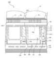


Classifications
-
- H—ELECTRICITY
- H10—SEMICONDUCTOR DEVICES; ELECTRIC SOLID-STATE DEVICES NOT OTHERWISE PROVIDED FOR
- H10K—ORGANIC ELECTRIC SOLID-STATE DEVICES
- H10K59/00—Integrated devices, or assemblies of multiple devices, comprising at least one organic light-emitting element covered by group H10K50/00
- H10K59/60—OLEDs integrated with inorganic light-sensitive elements, e.g. with inorganic solar cells or inorganic photodiodes
- H10K59/65—OLEDs integrated with inorganic image sensors
-
- G—PHYSICS
- G02—OPTICS
- G02B—OPTICAL ELEMENTS, SYSTEMS OR APPARATUS
- G02B5/00—Optical elements other than lenses
- G02B5/30—Polarising elements
-
- G—PHYSICS
- G06—COMPUTING OR CALCULATING; COUNTING
- G06T—IMAGE DATA PROCESSING OR GENERATION, IN GENERAL
- G06T1/00—General purpose image data processing
-
- G—PHYSICS
- G06—COMPUTING OR CALCULATING; COUNTING
- G06T—IMAGE DATA PROCESSING OR GENERATION, IN GENERAL
- G06T7/00—Image analysis
-
- G—PHYSICS
- G06—COMPUTING OR CALCULATING; COUNTING
- G06V—IMAGE OR VIDEO RECOGNITION OR UNDERSTANDING
- G06V10/00—Arrangements for image or video recognition or understanding
- G06V10/10—Image acquisition
- G06V10/12—Details of acquisition arrangements; Constructional details thereof
- G06V10/14—Optical characteristics of the device performing the acquisition or on the illumination arrangements
- G06V10/143—Sensing or illuminating at different wavelengths
-
- G—PHYSICS
- G06—COMPUTING OR CALCULATING; COUNTING
- G06V—IMAGE OR VIDEO RECOGNITION OR UNDERSTANDING
- G06V10/00—Arrangements for image or video recognition or understanding
- G06V10/10—Image acquisition
- G06V10/12—Details of acquisition arrangements; Constructional details thereof
- G06V10/14—Optical characteristics of the device performing the acquisition or on the illumination arrangements
- G06V10/147—Details of sensors, e.g. sensor lenses
-
- G—PHYSICS
- G06—COMPUTING OR CALCULATING; COUNTING
- G06V—IMAGE OR VIDEO RECOGNITION OR UNDERSTANDING
- G06V40/00—Recognition of biometric, human-related or animal-related patterns in image or video data
- G06V40/10—Human or animal bodies, e.g. vehicle occupants or pedestrians; Body parts, e.g. hands
- G06V40/12—Fingerprints or palmprints
- G06V40/13—Sensors therefor
- G06V40/1318—Sensors therefor using electro-optical elements or layers, e.g. electroluminescent sensing
-
- G—PHYSICS
- G06—COMPUTING OR CALCULATING; COUNTING
- G06V—IMAGE OR VIDEO RECOGNITION OR UNDERSTANDING
- G06V40/00—Recognition of biometric, human-related or animal-related patterns in image or video data
- G06V40/10—Human or animal bodies, e.g. vehicle occupants or pedestrians; Body parts, e.g. hands
- G06V40/12—Fingerprints or palmprints
- G06V40/13—Sensors therefor
- G06V40/1324—Sensors therefor by using geometrical optics, e.g. using prisms
-
- G—PHYSICS
- G06—COMPUTING OR CALCULATING; COUNTING
- G06V—IMAGE OR VIDEO RECOGNITION OR UNDERSTANDING
- G06V40/00—Recognition of biometric, human-related or animal-related patterns in image or video data
- G06V40/10—Human or animal bodies, e.g. vehicle occupants or pedestrians; Body parts, e.g. hands
- G06V40/12—Fingerprints or palmprints
- G06V40/1347—Preprocessing; Feature extraction
-
- G—PHYSICS
- G06—COMPUTING OR CALCULATING; COUNTING
- G06V—IMAGE OR VIDEO RECOGNITION OR UNDERSTANDING
- G06V40/00—Recognition of biometric, human-related or animal-related patterns in image or video data
- G06V40/10—Human or animal bodies, e.g. vehicle occupants or pedestrians; Body parts, e.g. hands
- G06V40/12—Fingerprints or palmprints
- G06V40/1365—Matching; Classification
-
- G—PHYSICS
- G06—COMPUTING OR CALCULATING; COUNTING
- G06V—IMAGE OR VIDEO RECOGNITION OR UNDERSTANDING
- G06V40/00—Recognition of biometric, human-related or animal-related patterns in image or video data
- G06V40/10—Human or animal bodies, e.g. vehicle occupants or pedestrians; Body parts, e.g. hands
- G06V40/14—Vascular patterns
-
- H—ELECTRICITY
- H04—ELECTRIC COMMUNICATION TECHNIQUE
- H04N—PICTORIAL COMMUNICATION, e.g. TELEVISION
- H04N25/00—Circuitry of solid-state image sensors [SSIS]; Control thereof
- H04N25/70—SSIS architectures; Circuits associated therewith
-
- H—ELECTRICITY
- H05—ELECTRIC TECHNIQUES NOT OTHERWISE PROVIDED FOR
- H05B—ELECTRIC HEATING; ELECTRIC LIGHT SOURCES NOT OTHERWISE PROVIDED FOR; CIRCUIT ARRANGEMENTS FOR ELECTRIC LIGHT SOURCES, IN GENERAL
- H05B33/00—Electroluminescent light sources
- H05B33/02—Details
-
- H—ELECTRICITY
- H10—SEMICONDUCTOR DEVICES; ELECTRIC SOLID-STATE DEVICES NOT OTHERWISE PROVIDED FOR
- H10F—INORGANIC SEMICONDUCTOR DEVICES SENSITIVE TO INFRARED RADIATION, LIGHT, ELECTROMAGNETIC RADIATION OF SHORTER WAVELENGTH OR CORPUSCULAR RADIATION
- H10F39/00—Integrated devices, or assemblies of multiple devices, comprising at least one element covered by group H10F30/00, e.g. radiation detectors comprising photodiode arrays
- H10F39/10—Integrated devices
- H10F39/12—Image sensors
-
- H—ELECTRICITY
- H10—SEMICONDUCTOR DEVICES; ELECTRIC SOLID-STATE DEVICES NOT OTHERWISE PROVIDED FOR
- H10K—ORGANIC ELECTRIC SOLID-STATE DEVICES
- H10K59/00—Integrated devices, or assemblies of multiple devices, comprising at least one organic light-emitting element covered by group H10K50/00
- H10K59/10—OLED displays
- H10K59/12—Active-matrix OLED [AMOLED] displays
- H10K59/13—Active-matrix OLED [AMOLED] displays comprising photosensors that control luminance
-
- H—ELECTRICITY
- H10—SEMICONDUCTOR DEVICES; ELECTRIC SOLID-STATE DEVICES NOT OTHERWISE PROVIDED FOR
- H10K—ORGANIC ELECTRIC SOLID-STATE DEVICES
- H10K59/00—Integrated devices, or assemblies of multiple devices, comprising at least one organic light-emitting element covered by group H10K50/00
- H10K59/40—OLEDs integrated with touch screens
-
- H—ELECTRICITY
- H10—SEMICONDUCTOR DEVICES; ELECTRIC SOLID-STATE DEVICES NOT OTHERWISE PROVIDED FOR
- H10K—ORGANIC ELECTRIC SOLID-STATE DEVICES
- H10K59/00—Integrated devices, or assemblies of multiple devices, comprising at least one organic light-emitting element covered by group H10K50/00
- H10K59/80—Constructional details
- H10K59/875—Arrangements for extracting light from the devices
- H10K59/878—Arrangements for extracting light from the devices comprising reflective means
-
- H—ELECTRICITY
- H10—SEMICONDUCTOR DEVICES; ELECTRIC SOLID-STATE DEVICES NOT OTHERWISE PROVIDED FOR
- H10K—ORGANIC ELECTRIC SOLID-STATE DEVICES
- H10K59/00—Integrated devices, or assemblies of multiple devices, comprising at least one organic light-emitting element covered by group H10K50/00
- H10K59/80—Constructional details
- H10K59/875—Arrangements for extracting light from the devices
- H10K59/879—Arrangements for extracting light from the devices comprising refractive means, e.g. lenses
-
- H—ELECTRICITY
- H10—SEMICONDUCTOR DEVICES; ELECTRIC SOLID-STATE DEVICES NOT OTHERWISE PROVIDED FOR
- H10K—ORGANIC ELECTRIC SOLID-STATE DEVICES
- H10K59/00—Integrated devices, or assemblies of multiple devices, comprising at least one organic light-emitting element covered by group H10K50/00
- H10K59/80—Constructional details
- H10K59/8791—Arrangements for improving contrast, e.g. preventing reflection of ambient light
- H10K59/8792—Arrangements for improving contrast, e.g. preventing reflection of ambient light comprising light absorbing layers, e.g. black layers
Definitions
- This disclosure relates to electronic devices.
- Optical fingerprint sensors are often installed in electronic devices such as smartphones, mobile phones, and PCs (Personal Computers).
- the optical fingerprint sensor irradiates light to image the surface of the finger for the required operation specifications and events such as waking from sleep, extracts the fingerprint features from the obtained image, and stores it in advance. It is judged whether or not the person is registered by collating with the existing information.
- biometric authentication such as skin color spectrum, vein information, and blood flow pulsation.
- fingerprint authentication and biometric authentication may deteriorate in authentication accuracy due to noise light generated from other than the subject.
- noise light There are two main types of noise light: external noise caused by light from outside the display and light emitted when imaging a subject are reflected and scattered inside an electronic device without going through the subject, and are sensed by the image pickup device. It's noise.
- One aspect of the present disclosure provides an electronic device capable of suppressing the influence of internally reflected light in the apparatus.
- the first polarizing plate that converts the incident light into linearly polarized light
- a first quarter wave plate whose slow axis differs from the absorption axis of the first polarizing plate by 45 degrees or 135 degrees.
- Self-luminous element layer and The first quarter wave plate and the second quarter wave plate having the same direction of the slow axis as the first quarter wave plate.
- a second polarizing plate whose absorption axis is orthogonal to the first polarizing plate, An image pickup device that captures light through the second polarizing plate, and an image pickup device. Electronic devices are provided.
- the first polarizing plate that converts the incident light into linearly polarized light
- a first quarter wave plate whose slow axis differs from the absorption axis of the first polarizing plate by 45 degrees or 135 degrees.
- An image pickup device that captures light through the second polarizing plate, and an image pickup device.
- Electronic devices are provided.
- the second polarizing plate may be provided in the pixel structure of the image pickup apparatus.
- the self-luminous element layer is a display having a self-luminous element.
- the image pickup device is an image pickup device that captures the scattered light of a finger irradiated with the light of the self-luminous element through the first quarter wave plate and the first polarizing plate.
- the scattered light of the finger is the first polarizing plate, the first quarter wave plate, the self-luminous element layer, the second quarter wave plate, and the second polarizing plate.
- the image pickup device is an image pickup device that captures an image of an authentication target irradiated with light from the self-luminous element layer via the first quarter wave plate and the first polarizing plate.
- the light from the target is the first polarizing plate, the first quarter wave plate, the self-luminous element layer, the second quarter wave plate, and the second polarizing plate.
- Imaged through The image pickup device outputs an image signal based on incident light incident through optical members having different wavelength transmission characteristics. If there is no rising edge in the wavelength region of 500 to 600 nanometers based on the image signal, an authentication unit for determining that the image pickup target is an artificial object may be further provided.
- the image pickup device is an image pickup device that captures an image of an authentication target irradiated with light from the self-luminous element layer via the first quarter wave plate and the first polarizing plate.
- the light from the target is the first polarizing plate, the first quarter wave plate, the self-luminous element layer, the second quarter wave plate, and the second polarizing plate.
- the self-luminous element layer may be an organic light emitting diode.
- the image pickup device is On-chip lens and A metal light-shielding film portion having a pinhole corresponding to the position where the on-chip lens collects light, May have.
- the image pickup device is Metal wire grid polarizing element, You may also have more.
- the metal wire grid polarizing element is It may be provided in the pinhole.
- the image pickup apparatus has a pixel array composed of a plurality of pixels.
- the pixel is A plurality of sub-pixels having a photoelectric conversion element that receives light incident at a predetermined angle and outputs an analog signal based on the intensity of the received light.
- An on-chip lens that concentrates the incident light on the sub-pixels, May have.
- a polarizing element may be configured in at least one of the subpixels.
- the polarizing element may be a wire grid polarizing element made of metal.
- the wire grid polarizing element may be a structure in which a light reflecting layer made of a first conductive material and a light absorbing layer made of a second conductive material are laminated above the reflection layer.
- the image pickup device has a color filter in the pixel, and the image pickup device has a color filter.
- the difference between the wavelength corresponding to the spectral centroid of the color filter and the wavelength corresponding to the emission spectral centroid of the self-luminous element layer at the time of authentication may be ⁇ 50 nm or less.
- the second polarizing plate includes a reflection type polarizing filter, an absorption type polarizing filter, and the like. May be laminated.
- the second polarizing plate has a wire grid polarizing element and has a wire grid polarizing element.
- the structure may be a structure in which a light reflecting layer made of a first conductive material and a light absorbing layer made of tungsten or a tungsten compound are laminated above the light reflecting layer.
- the target wavelength is 4 ⁇ T ⁇ (ne-no).
- the difference from the center of gravity of the emission spectrum of the self-luminous element layer at the time of authentication may be 0.05 um or less.
- the light emission of the self-luminous element layer at the time of authentication is other than white
- the thickness of the first quarter wave plate is T1 [um]
- the thickness of the second quarter wave plate is T1 [um].
- the first and second quarter wave plates are made of the same material, and the regularity when T1 [um] is divided by 60 and T2 [um]. May be different when divided by 60.
- the self-luminous element layer may emit light in an irradiation range limited to the irradiation range at the time of failed authentication, depending on the position where the living body is placed.
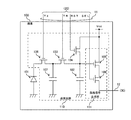
- the image pickup device is The light receiving part for each pixel and Charge storage part and A transistor that transfers the signal charge stored in the light receiving unit to the charge storage unit, and May have.
- a light-shielding metal may be arranged above the charge storage portion, and the light-shielding metal may have a pinhole shape on the light-receiving portion for each pixel.
- a light-shielding metal may be arranged above the charge storage unit, and the light-shielding metal may form a wire grid type polarizing element on the light-receiving part for each pixel.
- a light-shielding metal is arranged above the charge storage portion, the light-shielding metal has a pinhole shape on the light-receiving portion for each pixel, and a wire grid type polarizing element is provided in the pinhole. May be formed.
- the photographing device may be authenticated by a flip operation in biometric authentication.
- An authentication unit having a barcode reader function for authenticating a geometric shape based on an image captured by the image pickup device may be further provided.
- the authentication unit may be able to authenticate a shooting target that is moving relative to the image pickup device.
- FIG. 1 Schematic cross-sectional view of the electronic device according to the first embodiment.
- (A) is a schematic external view of the electronic device of FIG. 1
- (b) is a cross-sectional view of (a) in the direction of line AA.
- the block diagram which shows the structural example of the image pickup part.
- the block diagram which shows the composition example by the sub-pixel of the image pickup part.
- the figure which shows the example of the photoelectric conversion element separation part Schematic perspective view of a wire grid polarizing element composed of a wire grid.
- a conceptual diagram for explaining light and the like passing through a wire grid polarizing element Schematic diagram of the configuration when the image pickup unit is a fingerprint sensor. The figure explaining the details of an optical characteristic such as a polarization state in an optical path. The figure explaining the details of an optical characteristic such as a polarization state in an optical path.
- a schematic configuration example of an electronic device which is an example of an image pickup device. Block diagram of the signal processing unit. The figure which shows the reflectance of the skin surface. The flowchart which shows the processing flow of the electronic device 1. Schematic cross-sectional view of an electronic device. Top view of the reflector. The schematic diagram in the case of constructing a polarizing plate in a fingerprint sensor.
- the figure which shows the cross-sectional structure of a pixel when a polarizing plate is formed in a fingerprint sensor The figure which shows the structural example of the polarizing plate which concerns on 2nd Embodiment.
- the schematic diagram in the case of further constructing a quarter wave plate in a fingerprint sensor.
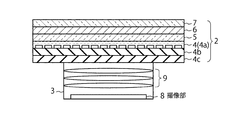
- FIG. 1A is a schematic cross-sectional view of the electronic device 1 according to the first embodiment.
- the electronic device 1 in FIG. 1A is an example of an electronic device 1 having an optical system, and is an arbitrary electronic device having both a display function and a shooting function, such as a smartphone, a mobile phone, a tablet, a barcode reader, and a PC, and is a module. It is equipped with a lens 9.
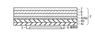
- FIG. 1B is a schematic cross-sectional view showing an example of an electronic device 1 having no module lens.
- the electronic device 1 of FIGS. 1A and 1B includes a camera module (imaging unit) arranged on the side opposite to the display surface of the display unit 2. As described above, the electronic device 1 of FIG. 1 is provided with the camera module 3 on the back side of the display surface of the display unit 2. Therefore, the camera module 3 shoots through the display unit 2.
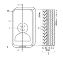
- FIG. 2 (a) is a schematic external view of the electronic device 1 of FIG. 1
- FIG. 2 (b) is a cross-sectional view taken along the line AA of FIG. 2 (a).
- the display screen 1a extends close to the external size of the electronic device 1, and the width of the bezel 1b around the display screen 1a is set to several mm or less.
- a front camera is often mounted on the bezel 1b, but in FIG. 2A, as shown by a broken line, a camera module 3 that functions as a front camera on the back surface side of a substantially central portion of the display screen 1a. Is placed.
- the camera module 3 is arranged on the back surface side of the substantially central portion of the display screen 1a, but in the present embodiment, the camera module 3 may be on the back surface side of the display screen 1a, for example, the display screen 1a.
- the camera module 3 may be arranged on the back surface side near the peripheral portion of the camera module 3.
- the camera module 3 in the present embodiment is arranged at an arbitrary position on the back surface side overlapping with the display screen 1a.
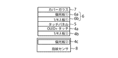
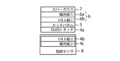
- the display unit 2 may include a polarizing plate 4c, a quarter wave plate 4b, a display panel 4 (4a), a touch panel 5, a circular polarizing plate 6, and a cover glass 7 (a touch panel may be included). ) Are stacked in order. Further, the circularly polarizing plate 6 has a polarizing plate 6a and a quarter wave plate 6b (see FIG. 9) as described later.
- the polarizing plate 4c and the quarter wave plate 4b suppress the internally reflected light from being incident on the camera module 3. Details of the polarizing plate 4c and the quarter wave plate 4b will be described later.
- the display panel 4 may be, for example, an organic light emitting diode (OLED: Organic Light Emitting Device), a liquid crystal display unit, a MicroLED, or a display panel based on other display principles.
- the display panel 4 such as the OLED unit is composed of a plurality of layers.
- the display panel 4 is often provided with a member having a low transmittance such as a color filter layer.
- a through hole may be formed in the member having a low transmittance in the display panel 4 according to the arrangement location of the camera module 3. If the subject light passing through the through hole is incident on the camera module 3, the image quality of the image captured by the camera module 3 can be improved.
- the circularly polarizing plate 6 is provided to reduce glare and improve the visibility of the display screen 1a even in a bright environment.
- a touch sensor is incorporated in the touch panel 5. There are various types of touch sensors such as a capacitance type and a resistance film type, and any method may be used. Further, the touch panel 5 and the display panel 4 may be integrated.
- the cover glass 7 is provided to protect the display panel 4 and the like.
- FIG. 3 is a block diagram showing a configuration example of the imaging unit 8.
- the image pickup unit 8 includes a pixel array unit 10, a vertical drive unit 20, a column signal processing unit 30, and a control unit 40.
- the pixel array unit 10 has a plurality of pixels 100. That is, the plurality of pixels 100 are arranged in a two-dimensional grid pattern.
- the pixel 100 generates an image signal according to the irradiated light.
- the pixel 100 has a photoelectric conversion unit that generates an electric charge according to the irradiated light.
- the pixel 100 further has a pixel circuit. This pixel circuit generates an image signal based on the electric charge generated by the photoelectric conversion unit. The generation of the image signal is controlled by the control signal generated by the vertical drive unit 20 described later.
- the signal lines 11 and 12 are arranged in the pixel array unit 10 in an XY matrix.
- the signal line 11 is a signal line that transmits a control signal of the pixel circuit in the pixel 100, is arranged for each row of the pixel array unit 10, and is commonly wired to the pixel 100 arranged in each row.
- the signal line 12 is a signal line for transmitting an image signal generated by the pixel circuit of the pixel 100, is arranged for each row of the pixel array unit 10, and is commonly wired to the pixel 100 arranged in each row. To. These photoelectric conversion units and pixel circuits are formed on a semiconductor substrate.
- the vertical drive unit 20 generates a control signal for the pixel circuit of the pixel 100.
- the vertical drive unit 20 transmits the generated control signal to the pixel 100 via the signal line 11 in the figure.
- the column signal processing unit 30 processes the image signal generated by the pixel 100.
- the column signal processing unit 30 processes the image signal transmitted from the pixel 100 via the signal line 12 in the figure.
- the processing in the column signal processing unit 30 corresponds to, for example, analog-to-digital conversion for converting an analog image signal generated in the pixel 100 into a digital image signal.
- the image signal processed by the column signal processing unit 30 is output as an image signal of the image pickup device 1.
- the control unit 40 controls the entire image pickup unit 8.
- the control unit 40 generates a control signal for controlling the vertical drive unit 20 and the column signal processing unit 30, and controls the pixel (image sensor) 100.
- the control signal generated by the control unit 40 is transmitted to the vertical drive unit 20 and the column signal processing unit 30 by the signal lines 41 and 42, respectively.
- FIG. 4 is a diagram showing an example of the cross-sectional structure of the pixel 100 shown in FIG. Pixels 100a and 100b show a side-by-side pixel example of the pixel array unit 10.
- an n-type semiconductor region is formed for each of the pixels 100a and 100b in, for example, a p-type semiconductor region of the semiconductor substrate 112.
- the photoelectric conversion element PD is formed in pixel units.
- a multilayer wiring layer composed of a transistor for reading out charges accumulated in the photoelectric conversion element PD and an interlayer insulating film is formed on the surface side (lower side in the figure) of the semiconductor substrate 112, a multilayer wiring layer composed of a transistor for reading out charges accumulated in the photoelectric conversion element PD and an interlayer insulating film is formed.
- An insulating layer 46 having a negative fixed charge is formed at the interface on the back surface side (upper side in the figure) of the semiconductor substrate 112.
- the insulating layer 46 is composed of a plurality of layers having different refractive indexes, for example, two layers of a hafnium oxide (HfO2) film 48 and a tantalum pentoxide (Ta2O5) film 47, and the insulating layer 46 is electrically pinned. By strengthening, it suppresses dark current and optically functions as an antireflection film.
- a silicon oxide film 49 is formed on the upper surface of the insulating layer 46, and a first light-shielding film portion 50 on which a pinhole 50a is formed is formed on the silicon oxide film 49.
- the first light-shielding film portion 50 may be a material that shields light from light, and is a material that has strong light-shielding properties and can be processed with high precision by fine processing, for example, etching. It is preferably formed of a titanium (Ti) or copper (Cu) film. Alternatively, they may be provided by an alloy thereof or a multilayer film of these metals.
- the first light-shielding film portion 50 forms a pinhole 50a and suppresses color mixing between pixels and light of a flare component incident at an unexpected angle.
- a light-shielding wall 61 and a plurality of layers of flattening films 62A and B having high light transmittance are formed in a plurality of stages. More specifically, the first light-shielding wall 61A is formed on a part of the first light-shielding film portion 50 between pixels, and the first flattening film 62A is formed between the first light-shielding walls 61A. It is formed. Further, a second light-shielding wall 61B and a second flattening film 62B are formed on the first light-shielding wall 61A and the first flattening film 62A.
- the light-shielding wall referred to here is provided with a metal such as tungsten (W), titanium (Ti), aluminum (Al), or copper (Cu), an alloy thereof, or a multilayer film of the metals. May be good.
- a metal such as tungsten (W), titanium (Ti), aluminum (Al), or copper (Cu), an alloy thereof, or a multilayer film of the metals. May be good.
- it may be provided with an organic light-shielding material such as carbon black.
- even if it is a transparent inorganic film it may have a structure that suppresses crosstalk by a total reflection phenomenon due to a difference in refractive index, and may have a shape in which the uppermost portion is closed as, for example, an Air Gap structure. In order to close the uppermost portion as the Air Gap structure, a film forming method having poor coverage, for example, sputtering can be used.
- a color filter 71 is formed for each pixel on the upper surfaces of the second light-shielding wall 61B and the second flattening film 62B.
- each color of R (red), G (green), and B (blue) is arranged by, for example, a Bayer arrangement, but may be arranged by another arrangement method.
- the image pickup unit 8 may be configured without arranging the color filter 71.
- the on-chip lens 72 is formed for each pixel on the color filter 71.
- the on-chip lens 72 may be made of an organic material such as a styrene resin, an acrylic resin, a styrene-acrylic copolymer resin, or a siloxane resin.
- the refractive index of the styrene resin is about 1.6, and the refractive index of the acrylic resin is about 1.5.
- the refractive index of the styrene-acrylic copolymer resin is about 1.5 to 1.6, and the refractive index of the siloxane resin is about 1.45.
- it may be composed of an inorganic material such as SiN or SiON.
- the refractive index of SiN is about 1.9, and SiON has a refractive index between SiN and the silicon oxide film.
- a filter layer that transmits a specific wavelength such as cyan, magenta, or yellow may be provided in addition to red, green, and blue.
- the color filter 71 is not only composed of an organic material-based color filter layer using an organic compound such as a pigment or a dye, but also a photonic crystal or a wavelength selection element applying plasmon (a lattice-shaped hole structure in a conductor thin film). It can also be composed of a color filter layer having a conductor lattice structure provided with the above (see, for example, Japanese Patent Application Laid-Open No. 2008-177191) and a thin film made of an inorganic material such as amorphous silicon.
- the inner lens 1210 is made of an inorganic material such as SiN or SiON.
- the inner lens 1210 is formed on the formed first-stage light-shielding wall layer (first light-shielding wall 61A and first flattening film 62A.
- the inner lens is provided to increase the focusing power and beam. The spot diameter of the waist can be reduced.
- the inner lens may be provided in a plurality of stages in one pixel, or the image pickup unit 8 may be configured without the inner lens. In the light-collecting design, it is desirable to align the light-collecting point with the pinhole 50a of the first light-shielding film portion 50.
- the structure shown in FIG. 4 is merely an example.
- a pinhole 50a is formed by a wiring layer of a surface-illuminated image pickup device, and an on-chip lens or an inner lens is provided so as to align a focusing point with the pinhole. May be good.
- a pinhole 50a may be formed of a light-shielding metal of a CCD (charge-coupled device) to prevent smear, and an on-chip lens or an inner lens may be provided so as to align a condensing point with the pinhole.
- CCD charge-coupled device
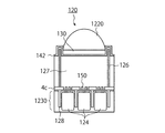
- FIG. 5 is a block diagram showing a configuration example of the subpixel 124 of the imaging unit 8. As shown in FIG. 5, the image pickup unit 8 is different from the image pickup unit 8 shown in FIG. 3 by reading a signal from the subpixel 124. Since the latter configuration is the same as that of the image pickup unit 8 shown in FIG. 3, the description thereof will be omitted.
- FIG. 6A is a diagram showing an example of the configuration of the sub-pixel 124.
- the pixel 120 is a wiring composed of a semiconductor substrate 123, a plurality of subpixels 124, a plurality of photoelectric conversion element separation portions 128 provided between the subpixels 124, and an insulating layer and a wiring layer.
- a layer 129, a lens 1220, and a light-shielding wall 126 between pixels are further provided.
- a plurality of sub-pixels 124 are provided for one pixel 120.
- the subpixel 124 is, for example, a photodiode.
- the number of subpixels 124 is not limited to this, and may be more or less than 25 as long as the processing can be performed appropriately.
- the sub-pixels 124 are all shown as the same square, but the present invention is not limited to this, and the sub-pixels 124 may have an appropriate shape based on the information to be acquired according to various situations. Alternatively, a different filter may be used for each sub-pixel 124 provided in the pixel 100.
- FIG. 6A is an example of a back-illuminated image sensor.
- a light ray vertical light
- an oblique direction direction not parallel to the optical axis of the lens 1220.
- the case where the light rays (diagonal lights 1 and 2) are incident is shown.
- a bundle (solid line) of parallel light rays incident from the upper part of the lens 1220 is focused on the subpixel 124 located at the center.
- the bundle (dotted line) of the light rays incident in the diagonal direction is focused on the subpixel 124 which is not the center.
- the vertical optical axis of the lens 1220 is used as a reference, but this is not always the case. Not limited to this, it may be determined in which direction the light ray is incident on the sub-pixel 124 located at the center of the pixel 120 by a pupil correction technique or the like described later.
- the semiconductor substrate 123 for example, a silicon substrate, forms a semiconductor region portion of an element constituting a pixel circuit.
- the elements of the pixel circuit are formed in the well region formed on the semiconductor substrate 123.
- the semiconductor substrate 123 in the figure is composed of a p-type well region.
- the pixel 120 has a plurality of photoelectric change elements 124, and the sub-pixel 124 is composed of an n-type semiconductor region and a p-type well region around the n-type semiconductor region.
- photoelectric conversion occurs.
- the electric charge generated by this photoelectric conversion is converted into an image signal by a pixel circuit (not shown).
- the semiconductor substrate 123 is further formed with a semiconductor region portion of a vertical drive unit, a column signal processing unit, and a control unit.
- the wiring layer 129 connects the semiconductor elements in the pixels to each other.
- the wiring layer 129 is also used for connection with a circuit outside the pixel and constitutes a signal line.
- the wiring of the wiring layer 129 is made of, for example, a metal such as copper or aluminum to transmit an electric signal, and the insulating layer is, for example, silicon oxide to insulate between the wirings.
- these insulating layers and wirings are formed adjacent to the front surface side of the semiconductor substrate 123 to form the wiring layer 129.
- a support substrate (not shown) is arranged adjacent to the wiring layer 129.
- This support substrate is a substrate that supports the image pickup device, and improves the strength of the image pickup device at the time of manufacture.
- a logic circuit or the like may be mounted on the support board in advance, and the semiconductor board 123 and the circuit of the support board may be electrically connected to each other as a laminated type.
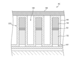
- FIG. 6B is a diagram showing an example of the photoelectric conversion element separation unit 128.
- the photoelectric conversion element separation unit 128 may be provided with a p-type well region 139. Further, a groove may be formed in the semiconductor substrate 123 so that the information regarding the light intensity is not propagated to the photoelectric conversion element of the adjacent subpixel (photoelectric conversion unit) 124, and the insulating film 141 may be provided in the groove. .. Further, a metal film 138 may be provided in addition to the insulating film 141. A film 140 having a negative fixed charge may be provided on the light receiving surface of the semiconductor substrate 123 and the trench side wall of the photoelectric conversion element separation portion 128.
- the negative fixed charge film 140 can be composed of, for example, an oxide containing at least one of hafnium, zirconium, aluminum, tantalum, and titanium, or a nitride.
- the insulating film 141 is made of, for example, silicon oxide or the like, and insulates the photoelectric conversion element of the subpixel 124 from the metal film 138.
- the metal film 138 has an opening in at least a part of the subpixel 124, and may be further embedded in the gap of the insulating film 141 in the trench portion of the photoelectric conversion element separation portion 128.
- the metal film 138 may be shielded from light so as to cover the black reference pixel region and the peripheral circuit region.
- the metal film 138 is a light-shielding material, for example, a metal film such as tungsten, aluminum, silver, gold, copper, platinum, molybdenum, chromium, titanium, nickel, iron and tellurium, a compound of these metals, or oxidation thereof. It can be composed of an article, or a nitride thereof, or an alloy thereof. Further, these materials may be combined as a multilayer film.
- the remaining width of the metal film 138 at the pixel 100 boundary is made thicker than the remaining width of the metal film 138 other than the pixel 100 boundary. You may prepare.
- the remaining width of the metal film 138 of the photoelectric conversion element separation portion 128 may be larger or thinner than the trench width formed on the semiconductor substrate 123.
- the former suppresses deterioration of dark current and white point characteristics, and improves angular resolution.
- the latter improves sensitivity.
- a part of the photoelectric conversion element separating portion 128 included in the pixel 100 is provided with the metal film 138 only in the gap of the insulating film 141 in the trench portion, and the metal film 138 is provided above the surface of the insulating film 141. It does not have to be.
- the interlayer film 127 is provided on the upper part of the metal film 138, and may be made of a transparent material such as silicon oxide, silicon nitride, or SiON.
- a transparent material such as silicon oxide, silicon nitride, or SiON.
- an organic material such as a styrene resin, an acrylic resin, a styrene-acrylic copolymer resin, or a sirosan resin may be used, and the lens 1220 is directly provided on the organic material. May be good.
- the light-shielding wall 126 may be provided so as to penetrate the interlayer film 127 at the boundary of the pixels 120. Stray light can be shielded by providing the light-shielding wall 126.
- the light-shielding wall 126 is made of a material having a light-shielding property, for example, a metal film such as tungsten, aluminum, silver, gold, copper, platinum, molybdenum, chromium, titanium, nickel, iron and tellurium, or a compound of these metals, or a compound thereof. It can be composed of oxides, or nitrides thereof, or alloys thereof. Further, it can also be configured as a multilayer film in which these materials are combined.
- the light-shielding wall 126 may be divided into multiple stages in the third direction. At the boundary of the pixel 100, these light-shielding walls 126 and the metal film 138 may be in continuous contact with each other.
- the color filter 130 uses, for example, a pigment or a dye as a material, transmits light of a desired wavelength, and can obtain spectral information of light from a subject.
- the color filter 130 may be provided, for example, on the interlayer film 127, or may be provided with an adhesion layer 142 that also serves as flattening between the interlayer film 127 and the color filter 130.
- the color filter 130 may be provided, for example, on the metal film 138, or may be provided with an adhesion layer that also serves as a flattening film between the metal film 138 and the color filter 130.
- the color filter 130 may be provided, for example, one for each subpixel 124, or they may be different for each subpixel 124. Alternatively, one color filter 130 may be provided for each pixel 100, and they may be different for each pixel 100. It is not necessary to provide a color filter with an emphasis on sensitivity and resolution.
- One lens 1220 is provided, for example, for each pixel 120.
- the lens 1220 may be composed of a plurality of laminated lenses.
- the lens can be made of an organic material such as a styrene resin, an acrylic resin, a styrene-acrylic copolymer resin, and a sirosan resin. It can also be made of an inorganic material such as silicon nitride or silicon oxynitride. Antireflection films having different refractive indexes may be provided on the lens surface. Further, a flattening film made of an organic material, for example, an acrylic resin may be provided under the lens material for the base step.
- a transparent inorganic material flattened by CMP or the like for example, silicon oxide may be provided.
- an image pickup device having a pinhole in a pixel or an image pickup device having a plurality of subpixels in a pixel has been described as an example. , It may be a surface irradiation type.
- an organic photoelectric conversion film may be used instead of the photoelectric conversion element by pn junction in the semiconductor substrate.
- sufficient space can be secured when using a module lens, it is possible to acquire a subject image with less blur even if the image pickup device does not have a pinhole or a sub-pixel by designing the module lens. Yes, it does not exclude these combinations.
- the quarter wave plates 4b, 6b function by shifting the phase between the two vertically polarized components of the light wave.
- Typical quarter wave plates 4b and 6b are birefringent crystals such as quartz and mica in which the direction of the optical axis and the film thickness T are determined.
- a normal axis having a refractive index of no and an abnormal axis having a refractive index of ne are obtained.
- the normal axis is perpendicular to the optical axis and the anomalous axis is parallel to the optical axis.
- the quarter wave plate has a phase difference ⁇ ( ⁇ ) of 90 degrees
- the wavelength ⁇ can be expressed by Eq. (2). As described above, there is a correspondence relationship of the equation (2) between the wavelength ⁇ and the film thickness T of the quarter wave plate.
- the quarter wave plates 4b and 6b according to the present embodiment are set to a thickness such that the optical path difference of the light transmitted through the normal axis and the abnormal axis is one quarter wavelength. More specifically, in the case of biophotographing, for example, fingerprint or vein imaging, the emission color is set in advance. For example, when only the portion of the display panel 4a corresponding to the green (G) is illuminated, the thickness of the wavelength ⁇ is set to correspond to 550 nm.
- the thickness should be set so that the wavelength ⁇ corresponds to 500 nm. This makes it possible to perform bioimaging with higher accuracy.
- the difference between the wavelength ⁇ represented by the equation (2) and the center of gravity of the emission spectrum at the corresponding portion of the display panel 4a is, for example, 0.05 um or less. This makes it possible to bring the phase difference ⁇ ( ⁇ ) generated in the quarter wave plate closer to the design wavelength, and the authentication accuracy is further improved.
- the quarter wave plates 4b and 6b can be mainly composed of three types: true zero order (True Zero Order), multiple order (Multiple Order), and compound zero order (Compound Zero Order).
- a true zero-order wave plate can be configured as a true zero-order wave plate because a predetermined retardation (phase difference) can be obtained at the 0th order at the design wavelength. It is made by processing the plate thickness of one birefringent material to be extremely thin so that a specific phase difference can be obtained at the 0th order. For example, if only the portion corresponding to the green filter (G) is to be illuminated, a quarter wave plate at 550 nm is manufactured.
- the stability of the phase difference obtained for wavelength shift, temperature change, or oblique incidence is superior to multi-order and compound zero-order.
- this thin plate thickness may be damaged during fixing to the device or handling, and the yield may decrease.
- N is a natural number and an even number.
- T1 / 60 0.25 + N.
- the above-mentioned disadvantages of the multi-order type can be improved. It will be possible.
- the optical axes of two birefringent materials of the same material manufactured in multi-order are arranged so as to be orthogonal to each other. That is, in the equations (1) and (2), n is a natural number and an even number. As a result, the phase difference shift amounts generated for each material cancel each other out, so that the wavelength dependence and the temperature dependence on the obtained retardation can be reduced. However, it may be difficult to improve the incident angle dependence.
- the thickness T1 of the quarter wave plates 4b and 6b is configured to be 0 or a natural number when 15 is subtracted from T1 and divided by 60.
- the thickness T2 of the quarter wave plates 4b, 6b is configured to be 0 or a natural number when 12.5 is subtracted from T2 and divided by 54.3.
- the polarizing plate 6a As the polarizing plate 6a, an absorption type polarizing filter, a reflection type polarizing filter, a crystal system, a multilayer film system, or the like can be used.
- a film of a suitable vinyl alcohol-based polymer such as polyvinyl alcohol and partially formalized polyvinyl alcohol is dyed and stretched with a dichroic substance such as iodine and a dichroic dye. It is composed of a film which has been subjected to appropriate treatment such as cross-linking treatment in an appropriate order and method.
- appropriate treatment such as cross-linking treatment in an appropriate order and method.
- the film is stretched in the longitudinal direction. Therefore, in the obtained linear polarizing element, the polarization absorbing axis parallel to the longitudinal direction of the linear polarizing element and the width of the linear polarizing element are used. A polarization transmission axis parallel to the direction is obtained.
- the crystalline polarizing element 150 can be configured by, for example, a photonic crystal.
- a photonic crystal is a structure having a periodicity of the wavelength order of light in the refractive index. By controlling the period and shape of this structure, the transmittance on the transmission axis and the reflectance on the absorption axis can be set.
- the polarizing element 150 of the multilayer film system is composed of, for example, a multilayer film made of at least two or more kinds of film materials having different refractive indexes.
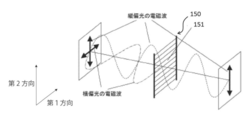
- FIG. 7 is a schematic perspective view of a so-called reflective wire grid polarizing element 150 configured by a wire grid.
- the polarizing element 150 in the figure represents an example of a polarizing element configured by a wire grid.
- the wire grid polarizing element 150 is a polarizing unit composed of strip-shaped conductors 151 arranged at a predetermined pitch. In the wire grid-shaped metal film, the polarized light in the direction (longitudinal direction) that the free electrons in the metal follow is canceled by the reflected wave, and the polarized light in the direction that does not follow (shortward direction) is transmitted.
- the pitch of the wire grid polarizing element is preferably less than 1/2 of the wavelength used, and if it exceeds this, diffracted light is generated.
- the band-shaped conductor 151 may be provided with the light reflecting layer 51 as a single layer, or the light absorbing layer 53 may be laminated on the light reflecting layer 51. Alternatively, an insulating layer 52 may be provided between the light reflecting layer 51 and the light absorbing layer 53.
- the constituent material of the light reflecting layer 51 is not particularly limited as long as it is a material having reflectivity to light in the band used, and for example, Al, Pt, Ag, Cu, Mo, Cr, Ti, Ni, W, and the like. Elemental substances such as Fe, Si, Ge, and Te, or alloys containing one or more of these elements can be mentioned. Above all, when the polarizing plate is used for visible light applications, the reflective layer is preferably made of aluminum or an aluminum alloy.
- silver (Ag), copper (Cu), gold (Au) or the like in order to give polarization characteristics to a wavelength band other than visible light, for example, an infrared region. This is because the resonance wavelengths of these metals are in the vicinity of the infrared region.
- an inorganic film or a resin film other than the metal formed with high reflectance on the surface by coloring or the like may be used.
- the reflected light from the wire grid polarizing element 150 may cause flare due to scattering inside the housing and cause deterioration of the image quality of the image pickup apparatus, or when strong light such as the sun is reflected on the display, the reflectance with the peripheral members. There is a concern that the difference may give a sense of discomfort in appearance.
- a light absorption layer 53 may be provided on the light reflection layer 51.
- the extinction coefficient k is not zero, that is, a metal material or alloy material having a light absorption action, a semiconductor material, specifically, tungsten (W), silver (Ag), or gold.
- Al copper
- Mo molybdenum
- Cr chromium
- Ti titanium
- Ni nickel
- Fe iron
- Si silicon
- Ge germanium
- Te tellurium
- metal materials such as (Sn), alloy materials containing these metals, and semiconductor materials.
- silicide-based materials such as FeSi2 (particularly ⁇ -FeSi2), MgSi2, NiSi2, BaSi2, CrSi2, and CoSi2 can also be mentioned.
- the light reflecting layer 51 and the light absorbing layer 53 are formed by various chemical vapor deposition methods (CVD method), coating method, various physical vapor deposition methods (PVD method) including sputtering method and vacuum vapor deposition method, and sol-gel method. , It can be formed based on a known method such as a plating method, a MOCVD method, or an MBE method.
- CVD method chemical vapor deposition methods
- PVD method physical vapor deposition methods
- sol-gel method sol-gel method.
- It can be formed based on a known method such as a plating method, a MOCVD method, or an MBE method.
- SiOX-based materials such as SiO2, NSG (non-doped silicate glass), BPSG (boron-phosphorus silicate-glass), PSG, BSG, PbSG, AsSG, SbSG, SOG (spin-on glass) (Constituent material), SiN, SiON, SiOC, SiOF, SiCN, low dielectric constant insulating material (for example, fluorocarbon, cycloperfluorocarbon polymer, benzocyclobutene, cyclic fluororesin, polytetrafluoroethylene, amorphous tetrafluoroethylene, polyaryl) Ether, Fluoroaryl Ether, Fluoropolymer, Organic SOG, Parylene, Fluorocarbon, Amorphous Carbon), Polypolymer Resin, Fluororesin,
- Insulation film material a trademark of Flare (Honeywell Electrical Materials Co.), and a polyaryl ether (PAE) -based material
- the insulating layer 52 can be formed based on known methods such as various CVD methods, coating methods, various PVD methods including sputtering methods and vacuum vapor deposition methods, various printing methods such as screen printing methods, and sol-gel methods.
- the insulating layer 52 functions as a base layer of the light absorbing layer, and at the same time, adjusts the phase of the polarized light reflected by the light absorbing layer and the polarized light transmitted through the light absorbing layer and reflected by the light reflecting layer to interfere with each other.
- the insulating layer 52 has a thickness such that the phase in one round trip is shifted by half a wavelength.
- the thickness of the insulating layer may be determined based on the balance between the desired polarization characteristics and the actual manufacturing process, for example, 1 ⁇ 10-9 m to 1 ⁇ 10-7 m, more preferably 1 ⁇ . 10-8m to 8 ⁇ 10-8m can be exemplified.
- the refractive index of the insulating layer is larger than 1.0 and is not limited, but is preferably 2.5 or less.
- an anisotropic dry etching technique using a combination of a lithography technique and an etching technique for example, carbon tetrafluoride gas, sulfur hexafluoride gas, trifluoromethane gas, xenon difluoride gas, etc.
- a lithography technique for example, carbon tetrafluoride gas, sulfur hexafluoride gas, trifluoromethane gas, xenon difluoride gas, etc.
- lithography technology photolithography technology (lithography technology using g-line, i-line, KrF excimer laser, ArF excimer laser, EUV, etc.
- the strip-shaped conductor 151 can be formed based on a microfabrication technique using an extremely short-time pulse laser such as a femtosecond laser or a nanoimprint method.
- a dielectric layer or both a dielectric layer and an air layer may be provided between the wire grids.
- the material constituting the dielectric layer is not particularly limited, but from the viewpoint of suppressing unnecessary reflection of light rays to be polarized in the polarizing plate, for example, Si oxide such as SiO2, AlF2, BaF2, CeF3, LaF3 , LiF, MgF2, NdF3, NaF, YF3 and the like.
- FIG. 8 is a conceptual diagram for explaining light and the like passing through the wire grid polarizing element.
- the extending direction (first direction) of the band-shaped conductor 151 coincides with the absorption axis for quenching, and the repeating direction of the band-shaped conductor 151 (which is the second direction and is orthogonal to the first direction) is the transmission axis for transmitting.
- Match That is, the free electrons in the band-shaped conductor 151 vibrate following the electric field of the light incident on the band-shaped conductor 151, and radiate the reflected wave.
- the light perpendicular to the longitudinal direction of the band-shaped conductor (second direction) reduces the radiation of the reflected light from the band-shaped conductor. This is because the vibration of free electrons is limited and the amplitude becomes small.
- the incident light on the transmission axis (second direction) is less attenuated by the polarizing element 150 and can pass through the polarizing element 150.
- the reflectance with respect to the incident light changes depending on the optical thickness of the light reflecting layer 51 (refractive index ⁇ film thickness of the light reflecting layer). Further, the reflectance with respect to the incident light also changes depending on the optical thickness of the light absorbing layer 53 (absorption rate ⁇ film thickness of the light reflecting layer).
- FIG. 9 is a schematic diagram of a configuration when the image pickup unit 8 is a fingerprint sensor.
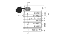
- the light emitted from the display panel (OLED) 4a irradiates the fingerprint along the optical path L1 and is imaged by the fingerprint sensor 8. That is, the light emitted from the OLED 4a (display panel 4) irradiates the finger through the touch panel 5, the quarter wave plate 6b, the polarizing plate 6a, and the cover glass 7, and the scattered light from the finger is the cover glass. 7.
- the image is captured by the fingerprint sensor 8 via the polarizing plate 6a, the quarter wave plate 6b, the touch panel 5, the OLED 4a, the quarter wavelength plate 4b, and the polarizing plate 4c.
- a part of the light emitted from the OLED 4a is reflected by the polarizing plate 6a along the optical path L2, and further passes through the quarter wave plate 6b, the touch panel 5, the OLED 4a, and the quarter wave plate 4b.
- the polarizing plate 4c is irradiated and reflected by the polarizing plate 4c.
- the quarter wave plate 4b and the polarizing plate 4c are further provided to suppress the noise component reflected along the optical path L2 from being incident on the fingerprint sensor 8.
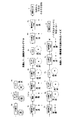
- FIG. 10 is a diagram illustrating details of optical characteristics such as polarization states in the optical paths L1 and L2.
- the absorption axis of the polarizing plate (1) can be arbitrarily provided, and the optical axis of the other optical members of FIG. 10 and FIG. 10 is defined relative to the polarizing plate (1).
- the transmission axis of the polarizing plate (1) is set to 0 degrees, and the sign of the angle is described by defining the clockwise direction in the + direction with respect to the traveling direction of light.
- the arrow at the bottom of FIG. 10 schematically shows the transmission axis.
- the transmission axis of the polarizing plate (1) that is, the polarized light set to 0 degrees is indicated by the up and down arrows, and the polarized light orthogonal to the polarizing plate (1) is indicated by the left and right arrows.
- FIG. 10 In the case of circularly polarized light, the traveling direction of light is unified toward the front of the paper surface, and the rotation direction of polarized light is indicated by an arc arrow. In the case of unpolarized light, it is shown that multiple arrows with different polarization directions are overwritten.
- the light emitted by the OLED 4a is applied to the fingerprint Fin via the touch panel 5, the quarter wave plate 6b, the polarizing plate 6a, and the cover glass 7.
- the slow axis of the quarter wave plate 6b is provided so as to be 45 ° (or 135 °).
- the transmission axis of the polarizing plate 6a is 0 degrees
- light with a polarization direction of 0 degrees is transmitted.
- the light scattered by the fingerprint Fin passes through the quarter wave plate 6b again as scattered light having a polarization direction of 0 degrees.
- the slow axis of the quarter wave plate 6b is 135 ° (or 45 °), and light with a polarization direction of 0 degrees is transmitted as circularly polarized light that rotates clockwise (or counterclockwise). do.
- the light transmitted through the quarter wave plate 6b further transmits through the touch panel 5 and the OLED 4a and is incident on the quarter wave plate 4b.
- the slow axis of the quarter wave plate 4b is provided to coincide with 6b.
- the traveling direction of the light it is 135 ° (or 45 °), so that the quarter wave plate 4b polarizes the incident light into linearly polarized light having a polarization direction of 90 degrees.
- the polarizing plate 4c is provided so that the absorption axis with the polarizing plate 6a is orthogonal to each other. Then, the 90-degree linearly polarized light transmitted through the quarter-wave plate 4b is transmitted through the polarizing plate 4c having a polarization direction of 90 degrees and is imaged by the fingerprint sensor 8.
- the noise light of the optical path L2 reflected by the polarizing plate 6a passes through the quarter wave plate 6b as polarized light in the 90-degree direction.
- the slow axis of the quarter wave plate 6b is 135 ° (or 45 °)
- light having a polarization direction of 90 degrees is transmitted as circularly polarized light that rotates counterclockwise (or clockwise).
- the light transmitted through the quarter wave plate 6b further transmits through the touch panel 5 and the OLED 4a and is incident on the quarter wave plate 4b.
- the slow axis of the quarter wave plate 4b is 135 ° (or 45 °), so the circularly polarized light of left-handed rotation (or right-handed rotation) is transmitted as linearly polarized light of 0 degree. ..
- the 0 degree linearly polarized light transmitted through the quarter wave plate 4b is reflected by the polarizing plate 4c having a polarization direction of 90 degrees and is not captured by the fingerprint sensor 8.
- the signal component from the fingerprint of the optical path L1 reaches the fingerprint sensor 8 and is imaged.
- the noise light of the optical path L2 reflected by the polarizing plate 6a is reflected by the polarizing plate 4c and cannot reach the fingerprint sensor 8.
- the signal component from the fingerprint can be imaged with the noise component reduced.
- a commercially available wire grid type polarizing plate has a reflectance of, for example, 50.6% for an unpolarized vertical incident, a transmittance of, for example, 45.3%, and a degree of polarization of transmitted light. Is 99.1 percent.
- the reflection component of the optical path L2 is 50.6%.
- the signal from the fingerprint is 41.0%, and the noise component due to the reflection of the polarizing plate 6a is 50.6%, that is, At an SN ratio of ⁇ 1.8 dB, the influence of noise becomes large. As a result, the identification accuracy is lowered.
- the quarter wave plate 4b and the polarizing plate 4c of the present embodiment are further provided and the above-mentioned wire grid type polarizing plate is used for the polarizing plate 4c
- a commercially available absorbent polarizing plate for example, a dichroic dye polarizing element
- a transmittance of, for example, 18.5% and the degree of polarization of transmitted light for unpolarized vertical incident. Is 99.1%.
- the reflection component of the optical path L2 is 5.1%.
- the signal from the fingerprint is 6
- the noise component due to the reflection of the polarizing plate 6a is 5.1% with respect to 0.8%, that is, the influence of noise is large at an SN ratio of 2.5 dB. As a result, the identification accuracy is lowered.
- the quarter-wave plate 4b and the polarizing plate 4c of the present embodiment are further provided, and the above-mentioned absorption-type polarizing plate is used for the polarizing plate 4c as the polarizing plate 4c.
- one of the polarizing plates 6a and 4c may be an absorption type and the other may be a wire grid type, and the combination is limited. It's not something to do.
- FIG. 11 is a diagram for explaining the details of optical characteristics such as the polarization state in the optical paths L1 and L2, and is provided so that the slow axes of the quarter wave plate 6b and 4b are orthogonal to each other, and the polarizing plate 6a, It differs from FIG. 10 in that the absorption axes of 4c are provided so as to coincide with each other.
- FIG. 11 FIG. 11
- the polarization component of the light emitted by the OLED 4a is evenly distributed in each direction.
- the light emitted by the OLED 4a is applied to the fingerprint Fin via the touch panel 5, the quarter wave plate 6b, the polarizing plate 6a, and the cover glass 7.
- the slow axis of the quarter wave plate 6b is provided so as to be 45 ° (or 135 °).
- the polarizing plate 6a Since the polarizing plate 6a has a polarization direction of 0 degrees, light having a polarization direction of 0 degrees is transmitted.
- the light scattered by the fingerprint Fin passes through the quarter wave plate 6b again as scattered light having a polarization direction of 0 degrees. Since the traveling direction of light is reversed, the slow axis of the quarter wave plate 6b is 135 ° (or 45 °), and light with a polarization direction of 0 degrees is transmitted as circularly polarized light that rotates clockwise (or counterclockwise). do.
- the light transmitted through the quarter wave plate 6b further transmits through the touch panel 5 and the OLED 4a and is incident on the quarter wave plate 4b.
- the slow axes of the quarter wave plate 4b are provided so as to be orthogonal to each other. Considering the traveling direction of the light, it is 135 ° (or 45 °), so that the quarter wave plate 4b polarizes the incident light into linearly polarized light having a polarization direction of 0 degree.
- the polarizing plate 4c is provided so that the absorption axis coincides with the polarizing plate 6a. Then, the linearly polarized light of 0 degree transmitted through the quarter wave plate 4b is transmitted through the polarizing plate 4c having a polarization direction of 0 degree and is imaged by the fingerprint sensor 8.
- the noise light of the optical path L2 reflected by the polarizing plate 6a passes through the quarter wave plate 6b as polarized light in the 90-degree direction.
- the slow axis of the quarter wave plate 6b is 135 ° (or 45 °)
- light having a polarization direction of 90 degrees is transmitted as circularly polarized light that rotates counterclockwise (or clockwise).
- the light transmitted through the quarter wave plate 6b further transmits through the touch panel 5 and the OLED 4a and is incident on the quarter wave plate 4b.
- the slow axis of the quarter wave plate 4b is 45 ° (or 135 °), so the circularly polarized light of left-handed rotation (or right-handed rotation) is transmitted as linearly polarized light of 90 degrees. ..
- the 90-degree linearly polarized light transmitted through the quarter-wave plate 4b is reflected by the polarizing plate 4c having a polarization direction of 0 degrees and is not captured by the fingerprint sensor 8.
- the signal component from the fingerprint of the optical path L1 reaches the fingerprint sensor 8 and is imaged.
- the noise light of the optical path L2 reflected by the polarizing plate 6a is reflected by the polarizing plate 4c and cannot reach the fingerprint sensor 8.
- the signal component from the fingerprint can be imaged with the noise component reduced.
- FIG. 12 is a block diagram showing a schematic configuration example of an electronic device 1 which is an example of an image pickup device to which the present technology can be applied.
- the electronic device 1 includes a display unit 2 (FIGS. 1A and 1B), an image pickup unit 8 (FIGS. 1A and 1B), a control unit 40 (FIG. 3), an operation input unit 1000, and a signal processing unit. It includes 1002, a storage unit 1004, an authentication unit 1006, and a result output unit 1008.
- the operation input unit 1000 receives an operation input from the user of the electronic device 1.
- the operation input unit 1000 is composed of, for example, a push button or a touch panel.
- the operation input received by the operation input unit 1000 is transmitted to the control unit 40 and the signal processing unit 1002. After that, processing according to the operation input, for example, processing such as fingerprint imaging is activated.
- control unit 40 sends a command to the image pickup unit to control the pixel array unit 10 (FIG. 3), sends a command to the display unit 2, and uses the light source of the display unit 2 to illuminate the subject. You can guess.
- the illumination light can change the balance of elements having different spectra of the display unit, for example, the three primary colors of red, blue, and green, and can change the light emitting area.
- a light source (not shown) other than the display unit 2 may be provided, and for example, light in an infrared region not included in the organic EL may be emitted. Infrared rays are suitable for acquiring vein information.
- the electronic device 1 is provided with the optical system 9 (FIG. 1A), autofocus can be performed.
- the autofocus is a system that detects the focal position of the optical system 9 and automatically adjusts it.
- this autofocus for example, a method of detecting the image plane phase difference by the phase difference pixels arranged in the image pickup unit 8 and detecting the focal position (image plane phase difference autofocus) can be used. It is also possible to apply a method (contrast autofocus) of detecting the position where the contrast of the image is highest as the focal position.
- the control unit 40 adjusts the position of the lens of the optical system 9 via the lens drive unit (not shown) based on the detected focal position, and performs autofocus.
- the control unit 40 can be configured by, for example, a DSP (Digital Signal Processor) equipped with firmware.
- DSP Digital Signal Processor
- the signal processing unit 1002 processes the image signal generated by the image pickup unit 8. This processing includes, for example, demosaic to generate an image signal of a color that is insufficient among the image signals corresponding to red, green, and blue for each pixel, noise reduction to remove noise of the image signal, addition processing of a plurality of pixels, and processing. Coding of image signals and the like are applicable.
- the signal processing unit 1002 can be configured by, for example, a microcomputer equipped with firmware.
- FIG. 13A is a block diagram of the signal processing unit 1002 according to the present embodiment.
- the signal processing unit 1002 includes an A / D conversion unit 502, a clamp unit 504, a color-coded output unit 506, a defect correction unit 508, a linear matrix unit 510, and a spectrum analysis unit 512. , And an image processing unit 518.
- the A / D conversion unit 502 (Analog to Digital Converter) converts the analog signal output from the image pickup unit 8 into a digital signal for each pixel.
- the clamp unit 504 executes, for example, a process relating to the level of the ground in the image.
- the clamp unit 504 defines, for example, a black level, and the defined black level is subtracted from the image data output from the A / D conversion unit 502 and output.
- the clamp unit 504 may set the ground level for each photoelectric conversion element provided in the pixel, and in this case, the ground correction of the signal value may be performed for each acquired photoelectric conversion element.
- the color-specific output unit 506 outputs the image data output from the clamp unit 504 for each color.
- the image pickup unit 8 is provided with R (red), G (green), and B (blue) filters in the pixel.
- the clamp unit 504 adjusts the ground level based on these filters, and the color-coded output unit 506 outputs the signal output by the clamp unit 504 for each color.
- the color-coded output unit 506 stores the data of the filter provided for each pixel in the image pickup unit 8. , You may output for each color based on this data.
- the image pickup unit 8 is provided with a color filter, but the present invention is not limited to this, and for example, an organic photoelectric conversion film may be used to identify colors.
- the defect correction unit 508 corrects defects in the image data. Defects in image data occur, for example, due to missing pixels or missing information due to defects in the photoelectric conversion element provided in the pixels, missing information due to saturation of light in the optical system 9, and the like.
- the defect correction unit 508 may execute the defect correction process by performing interpolation processing based on, for example, the information of the surrounding pixels or the received intensity of the peripheral photoelectric conversion element in the pixel.
- the linear matrix unit 510 performs correct color reproduction by executing a matrix operation on color information such as RGB.
- the linear matrix unit 510 is also referred to as a color matrix unit.
- the linear matrix unit 510 obtains a desired spectrum by, for example, performing an operation on a plurality of wavelengths.
- the linear matrix unit 510 performs an operation so as to output an output suitable for detecting skin color.
- the linear matrix unit 510 may be provided with a calculation path of a system different from that of the skin color, and may perform a calculation for acquiring vein information, for example.
- an operation may be performed so as to perform an output suitable for the vicinity of 760 nanometers.
- Veins are rich in reduced hemoglobin, which has a characteristic absorption spectrum near 760 nanometers.
- FIG. 13B is a diagram showing the reflectance of the skin surface.
- the vertical axis shows the reflectance, and the horizontal axis shows the wavelength.
- the skin color varies from individual to individual, but generally there is a rise in the wavelength region of 550 to 600 nanometers.
- the spectrum analysis unit 512 determines, for example, whether or not there is a rise in the spectrum peculiar to the skin, based on the data output by the linear matrix unit 510.
- the spectrum analysis unit 512 detects, for example, the rise of a signal of 550 to 600 nanometers in a range including 500 to 650 nanometers, so that the human finger is in contact with the cover glass 7, or in that case, the cover glass 7. It detects and outputs what the wavelength is.
- the range to be determined is not limited to the above range, and may be wider or narrower than this in an appropriate range. For example, it may be analyzed whether or not the reduced hemoglobin has a peak near 760 nanometers.
- the image processing unit 518 extracts the feature points of the fingerprint shape based on the image signal generated by the linear matrix unit 510. Further, the image processing unit 518 extracts the feature points of the veins based on the image signal generated by the linear matrix unit 510.
- the storage unit 1004 stores various data. The storage unit 1004 may store, for example, a frame which is an image signal for one screen, or may store data in the process of signal processing and authentication processing.
- the authentication unit 1006 executes personal authentication based on the data output by the signal processing unit 1002.
- the authentication unit 1006 executes personal authentication based on, for example, the rising wavelength analyzed by the spectrum analysis unit 512 and the fingerprint shape (feature point) based on the data output from the defect correction unit 508 or the like.
- the authentication unit 1006 may analyze the rhythm of the peak of the reduced hemoglobin near 760 nanometers, and if it is not rhythmic, it determines that the imaging target is an artificial object. In this way, the authentication unit 1006 can improve the biometric authentication accuracy by capturing the hemoglobin signal, that is, the rhythm of the heartbeat from the blood flow.
- Personal information may be stored in, for example, the authentication unit 1006 as a wavelength range, a fingerprint feature point, and a vein feature point, or may be stored in the storage unit 1004.
- the authentication unit 1006 can determine that the object is a finger and authenticate that the object is a memorized individual.
- the authentication unit 1006 acquires the shape characteristics of the fingerprint from the output from the image processing unit 518 and the like, and uses this information to determine whether or not the fingerprint matches the fingerprint to be authenticated. For example, the authentication unit 1006 determines whether or not the feature points of the fingerprint stored in the storage unit 1004 match the feature points of the authentication target.
- a general method can be used for fingerprint authentication.
- the authentication unit 1006 determines that the object in contact with the cover glass 7 is a living body by using this data.
- the authentication unit 1006 acquires the shape characteristics of the vein from the output from the image processing unit 518 and the like, and uses this information to determine whether or not the vein matches the vein to be authenticated. For example, the authentication unit 1006 authenticates whether or not the individual is a memorized individual by comparing a predetermined number of feature points extracted from the vein with the feature points stored in the storage unit 1004. A general method can be used for vein authentication.
- the result output unit 1008 outputs the personal authentication result based on the result output from the authentication unit 1006. For example, when the storage unit 1004 matches the recorded individual, the result output unit 1008 matches the recorded individual data when the finger in contact with the cover glass 7 at that timing matches the recorded individual data. , The authentication OK signal is output to the display unit 2, and in other cases, the authentication NG signal is output to the display unit 2.
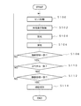
- FIG. 14 is a flowchart showing a processing flow of the electronic device 1 according to the present embodiment. As an example, a case where the electronic device 1 performs personal authentication by a fingerprint, a spectrum, and a vein will be described.
- the electronic device 1 activates the image pickup unit 8 as a fingerprint sensor (S100).
- the above-mentioned components may be energized and put into a standby state.
- the electronic device 1 may explicitly activate the fingerprint sensor by a switch or the like.
- it may be obtained optically or mechanically that an object is in contact with the reading surface (cover glass) 7, and the fingerprint sensor may be activated by this acquisition as a trigger.
- the reading surface (cover glass) 7 may be triggered by detecting that the finger approaches a distance closer than a predetermined distance.
- the imaging unit 8 detects the intensity of the incident light at that timing, and acquires the condition of the external light based on this result (S102). For example, the electronic device 1 acquires an image in a state where light from the inside is not incident. By this acquisition, the intensity of sunlight, the intensity of light transmitted by the indoor light source through the finger, or the intensity of light entering through the gap between the fingers is detected. Based on this light intensity, the clamp portion 504 may perform ground processing in a later process.
- the light emitting portion provided in the electronic device 1 emits light so as to irradiate at least a part of the area where the finger and the cover glass 7 are in contact with each other (S104).
- the light emission may be white light or light having a specific wavelength, for example, light emission of R, G, B or the like.
- B (and G) may be emitted in order to obtain the surface shape.
- Infrared light may also be emitted to observe the veins.
- R may be emitted for spectral analysis. In this way, the light emission may emit an appropriate color based on the subsequent processing. These lights do not have to be emitted at the same timing. For example, R may be emitted first to acquire data for spectrum analysis, and then B and G may be emitted to acquire data for shape analysis.
- the image pickup unit 8 receives the light emitted by the display panel 4a including information such as fingerprints and reflected by the cover glass 7 (S106).
- the light receiving is executed by the image pickup unit 8 described above, and then necessary processing is executed. For example, following the light reception, processing of acquiring the shape of the fingerprint and acquiring the spectrum of reflected light or transmitted light is executed via A / D conversion and background correction.
- the authentication unit 1006 determines whether the shapes of the fingerprints match (S108).
- the determination of the shape of the fingerprint may be performed by a general method. For example, the authentication unit 1006 extracts a predetermined number of feature points from the fingerprint and compares the extracted feature points to determine whether or not it can be determined that the individual is a memorized individual.
- the authentication unit 1006 may make the light emitting region of the light emitting unit 4a emit light only in the corresponding region at the position where the finger (living body) is placed. As a result, it is possible to suppress the generation of noise light having various reflection angles caused by causing the display panel (light emitting unit) 4a to emit light in a wide range. Therefore, the authentication accuracy is further improved.
- the authentication unit 1006 subsequently determines whether or not the spectra match (S110).
- the authentication unit 1006 performs this determination by comparing the result of the spectrum analyzed by the spectrum analysis unit 512 with the result of the stored individual. For example, it is determined whether or not the acquired spectrum exists within an allowable range from the stored spectrum of the rise of the skin color. In this way, personal authentication may be performed not only by the fingerprint shape but also by the spectrum.
- the authentication unit 1006 subsequently determines whether or not the vein shapes match (S112).
- the authentication unit 1006 performs this determination by comparing the feature points of the vein shape with the feature points of the memorized individual. In this way, personal authentication may be performed not only by the fingerprint shape but also by the spectrum and the vein shape.
- the authentication unit 1006 determines that the authentication was successful (S114), and outputs the authentication result from the result output unit 1008.
- the result output unit 1008 outputs that the authentication is successful, and permits access to other configurations of the electronic device 1, for example.
- the output is performed when the result output unit 1008 is successful, but the output is not limited to this. Even in the cases of S108: NO, S110: NO, and S112: NO described above, the light emitting unit, the imaging unit 8, etc. are notified via the result output unit 1008 that the authentication has failed, and data acquisition is performed again. You may.
- the above is a process of repeating when authentication fails. For example, when the process is repeated a predetermined number of times, access to the electronic device 1 is blocked without performing further authentication. You may. In this case, the interface may prompt the user to enter another access means, for example, a passcode using the numeric keypad. Further, in such a case, since there is a possibility that the reading of the device has failed, the authentication process may be repeated while changing the light emission, the light receiving light, the state of the reading surface, the spectrum used, and the like. For example, when the analysis result that the product is wet is obtained, some output may be output to the user via the interface in order to wipe off the water and perform the authentication operation again.
- the quarter wave plate 4b and the polarizing plate 4c are provided.
- the signal component from the fingerprint of the optical path L1 reaches the fingerprint sensor 8 is imaged, and the noise light of the optical path L2 reflected by the polarizing plate 6a is reflected by the polarizing plate 4c and cannot reach the fingerprint sensor 8. Therefore, the S / N ratio is improved, and the authentication accuracy of the authentication unit 1006 is improved.
- the first embodiment is a modification of the first embodiment in that when light is incident from the cover glass 7, the reflectance of the region of the imaging unit 8 and the reflectance of the other region are configured to match. It differs from the form. Hereinafter, the differences from the first embodiment will be described.
- FIG. 15 is a schematic cross-sectional view of the electronic device 1 according to the modified example of the first embodiment.
- the electronic device 1 has parts such as a battery, a communication circuit, a microphone, and a speaker (not shown), and is often provided under the display unit 2.
- the position and shape of each component may be visually recognized by the user, which may give a sense of discomfort in appearance.
- an opaque cover portion 4d is provided on the back surface side of the display portion 2. By using the opaque cover portion 4d, the parts provided under the display portion 2 are not visually recognized by the user.
- the cover portion 4d is used as a reflector, not only the problem of appearance can be solved, but also the brightness of the display portion 2 can be increased by the contribution of the reflected light.
- the cover portion 4d is often made of a material mainly made of a metal such as copper or aluminum.
- the opaque cover unit 4d cannot be provided directly above the display unit 2, and a window unit 4e for transmitting light is required.
- the window portion 4e may give an appearance of discomfort.
- a circularly polarizing plate 6 is provided, but there is no perfect polarizing plate or a quarter wave plate, and variations such as film thickness and angle error at the time of mounting also affect external light reflection. Is difficult to make completely zero.
- the electronic device 1 when light is incident from the cover glass 7, it is reflected by the cover portion 4d shown in FIG. 15 and goes out of the cover glass. It is configured so that the difference in the amount of light between the emitted light L3 and the light L4 through which the light passing through the window portion 4e is reflected and passing through the outside of the cover glass is small.
- the cover portion 4d when the cover portion 4d is provided as a reflector and is mainly made of a metal such as copper or aluminum, the polarizing plate 4c is provided with a reflective type, for example, a wire grid polarizing element. If the cover portion 4d is mainly made of aluminum, the reflective layer of the wire grid is also mainly made of aluminum, and if the cover portion 4d is mainly made of copper, the reflective layer of the wire grid is also mainly made of copper. It is more desirable to prepare the material so that the spectra of the reflected light are aligned.
- the transmission axis of the polarizing plate 4c so as to coincide with the above-mentioned linearly polarized light. Be prepared for. That is, even if the main material of the reflective layer of the wire grid is aligned with the cover portion 4d, it is difficult to contribute to reducing the difference in the amount of light between the light L3 and the light L4 as it is. As a countermeasure, the width of the metal portion of the wire grid polarizing element may be widened in order to increase the reflection of polarized light on the transmission axis.
- the wire grid polarizing element of the polarizing plate 4c has a sufficient thickness, at least 300 nanometers or more, and the width of the metal part is at least 200 nanometers or more, preferably 300 nanometers or more. By doing so, the effect of suppressing the appearance visibility can be recognized.
- the polarizing plate 4c may be provided as an absorption type.
- the absorption type is a PVA film dyed and stretched with an iodine-based material or a dye-based material such as a dichroic dye.
- the polarizing plate 4c may be provided by a wire grid polarizing element 150 provided with a light absorbing layer. More specifically, from FIG. 7, for example, a wire grid polarizing element 150 in which a light absorption layer 53 in which antireflection tungsten is formed is formed on a light reflection layer 51 made of aluminum having high reflectance is configured. The reflectance may be balanced by controlling the film thickness. As described above, since the wire grid polarizing element 150 has the light reflecting layer 51 and the light absorbing layer 53, the reflectance can be adjusted by adjusting the thickness and material of each of the light reflecting layer 51 and the light absorbing layer 53. .. Alternatively, in the polarizing plate 4c, the difference in reflectance may be reduced by forming the image pickup unit 8 side with a reflective polarizing element and the display unit 2 side with an absorption type polarizing element.
- the orthogonal relationship with the polarizing plate 6a is broken, and the amount of light emitted from the cover glass 7 can be changed.
- the region corresponding to the window portion 4e may be hollowed out by the quarter wave plate 4b, and another quarter wave plate having the same outer shape but out of phase may be fitted.
- the angle at which the visibility of the window portion 4e is lost may be obtained by an experiment.
- the display unit 2 has the same light reflectance in the vertically upper region of the imaging unit 8 and the light reflectance in the other regions. It was decided to adjust the material, thickness, angle, or line width of the optical element included in. As a result, even if the incident light is incident through the cover glass 7, the amount of reflected light reflected through the cover glass 7 is made uniform.
- the electronic device 1 according to the second embodiment is different from the electronic device 1 according to the first embodiment in that the polarizing plate 4c is configured in the fingerprint sensor 8.
- the differences from the electronic device 1 according to the first embodiment will be described.
- FIG. 17 is a schematic diagram in the case where the image pickup unit 8 is configured with the polarizing plate 4c in the fingerprint sensor 8.
- the polarizing plate 4c is configured in the fingerprint sensor 8.
- the optical characteristics of the quarter wave plates 4b and 6b and the polarizing plates 4c and 6a can be made equivalent to the optical characteristics shown in FIG. 10 or FIG. That is, as shown in FIG. 10, the slow axis of the quarter wave plate 6b differs from the transmission axis of the polarizing plate 6a by 45 degrees or 135 degrees. Further, the transmission axis of the polarizing plate 6a and the transmission axis of the polarizing plate 4c are orthogonal to each other.
- the slow axis of the quarter wave plate 6b and the quarter wave plate 4b are the same.
- the slow axis of the quarter wave plate 6b differs from the transmission axis of the polarizing plate 6a by 45 degrees or 135 degrees.
- the transmission axis of the polarizing plate 6a and the transmission axis of the polarizing plate 4c are the same.
- the slow axes of the quarter wave plate 6b and the quarter wave plate 4b are orthogonal to each other.
- FIG. 18 is a diagram showing an example of the cross-sectional structure of the pixel 100 when the image pickup unit 8 constitutes the polarizing plate 4c in the fingerprint sensor 8.
- the pixel 100 includes a polarizing plate 4c, a base insulating layer 46, a first light-shielding film portion 50, a bank portion 61C, a color filter 71, an on-chip lens 72, and a semiconductor substrate 1201.
- a separation region 140, a flattening film 183, an insulating layer 191, a wiring layer 192, and a support substrate 199 are provided.
- the insulating layer 191 and the wiring layer 192 form a wiring region.
- a first light-shielding film portion 50 having a pinhole 50a is formed on the photoelectric conversion portion (light receiving region) 101.
- the first light-shielding film unit 50 described above shields the charge holding unit 107, which will be described later, from light-shielding.
- a base insulating layer 46 having a flattening layer as a lower layer is formed on the first light-shielding film portion 50, and a polarizing plate 4c having a wire grid polarizing element 150, a color filter 71, and an on-chip lens 72 are formed on the base insulating layer 46. Will be done.
- the bank portion 61C is configured to include, for example, a metal film. It is possible to dam the lens material with the bank portion 61C by the reflow process when forming the reflow lens. For example, in the reflow process, the material of the reflow lens 72 is dammed over the entire area of the bank portion 61C, and the shape of the reflow lens 72 is stabilized.
- the semiconductor substrate 1201 is a substrate on which the semiconductor portion of the element constituting the pixel circuit is formed.
- the semiconductor portion of the device is formed in a well region formed on the semiconductor substrate 1201.
- the semiconductor substrate 1201 in the figure is configured in a p-shaped well region.
- the semiconductor portion of the element is formed.
- the n-type semiconductor region 121 constitutes a photoelectric conversion unit 101. More specifically, the photoelectric conversion unit 101 is configured by a photodiode composed of a pn junction at the interface between the n-type semiconductor region 121 and the p-type well region around the n-type semiconductor region 121. The electric charge generated by the photoelectric conversion is accumulated in the n-type semiconductor region 121.
- the n-type semiconductor region 122 constitutes a floating diffusion type charge holding unit 107.
- a MOS transistor 108 is arranged between the n-type semiconductor regions 121 and 122.
- the MOS transistor 108 has n-type semiconductor regions 121 and 122 as sources and drains, respectively, and a p-type well region between them as a channel.
- the gate 135 is arranged adjacent to the channel of the MOS transistor 108.
- the insulating layer 191 between the semiconductor substrate 1201 and the gate 135 corresponds to the gate insulating film.
- the semiconductor substrate 1201 can be configured to have a thickness of, for example, 3 ⁇ m. Further, a p-type semiconductor region for pinning can be arranged in the vicinity of the front surface of the back surface of the semiconductor substrate 1201. This makes it possible to reduce noise based on the interface state.
- a wiring region composed of a wiring layer 192 and an insulating layer 191 described later is arranged on the surface side of the semiconductor substrate 1201.
- a fixed charge film 1410 (not shown) for strengthening the above-mentioned pinning and an oxide film 142 (not shown) for protecting and insulating the semiconductor substrate 1201 are arranged on the back surface side of the semiconductor substrate 1201.
- the fixed charge film 1410 may be composed of, for example, an oxide or a nitride containing at least one of hafnium (Hf), aluminum (Al), zirconium (Zr), tantalum (Ta) and titanium (Ti). can. Further, the fixed charge film 1410 can be formed by vapor deposition (CVD), sputtering and atomic layer deposition (ALD). When ALD is adopted, it is possible to simultaneously form a SiO 2 film that reduces the interface state during the film formation of the fixed charge film 1410, which is preferable.
- ALD atomic layer deposition
- the fixed charge film 1410 may be made of hafnium oxynitride or aluminum oxynitride. Alternatively, silicon (Si) or nitrogen (N) may be added to the fixed charge film 1410 in an amount that does not impair the insulating property. Thereby, heat resistance and the like can be improved.
- the oxide film 142 may be composed of, for example, SiO 2. It is formed by ALD to a thickness of 100 nm or less, more preferably 30 to 60 nm.
- the wiring layer 192 is a conductor for wiring an element formed on the semiconductor substrate 1201.
- the wiring layer 192 is made of a metal such as Cu.
- the insulating layer 191 insulates the wiring layer 192.
- the insulating layer 191 can be made of an insulating material, for example, SiO 2 .
- the wiring layer 192 and the insulating layer 191 can be configured in multiple layers.
- the separation region 140 is an region that separates the photoelectric conversion unit 101 of the adjacent pixels 100.
- the separation region 140 is arranged near the boundary between the pixels 100, and the inflow of electric charges from the adjacent pixels 100 can be prevented by injecting the ion implanter. Further, by forming a trench in the separation region 140 and embedding insulating films having different refractive indexes, it is possible not only to prevent the inflow of electric charges but also to block light obliquely incident from the adjacent pixels 100.
- the trench is formed in the separation region 140, it may be processed from the back surface side to the front surface side of the semiconductor substrate 1201, and further, it may be processed so as to penetrate the semiconductor substrate 1201.
- the separation region 140 may be made of a material that shields light from the gap, for example, metal. More specifically, Al, silver (Ag), gold (Ag), copper (Cu), platinum (Pt), molybdenum (Mo), chromium (Cr), Ti, nickel (Ni), W, iron (Fe). And can be composed of alloys containing tellurium (Te) and the like and these metals. Further, a plurality of these materials can be laminated and configured. Further, Ti, titanium nitride (TiN), and a film in which these are laminated can be arranged as an adhesion layer between the oxide film 142 and the oxide film 142.
- the sensitivity of the pixel 100 can be improved, which is preferable. This is because Al has a relatively high reflectance, and the light transmitted through the photoelectric conversion unit 101 (n-type semiconductor region 121) and incident on the separation region 140 is reflected and returned to the photoelectric conversion unit 101.
- the separation region 140 by Al can be formed by a known method, for example, high temperature sputtering.
- the groove for arranging the separation region 140 can be formed, for example, by dry etching the semiconductor substrate 1201. By embedding the above-mentioned insulating film or metal material in this groove, the separation region 140 can be arranged. This can be done, for example, by PVD (Physical Vapor Deposition) such as sputtering or vacuum vapor deposition, CVD, plating and coating methods.
- PVD Physical Vapor Deposition
- the second separation region 143 is a separation region arranged between the photoelectric conversion unit 101 and the second charge holding unit 107.
- the second separation region 143 is arranged in the groove formed in the semiconductor substrate 1201. Unlike the separation region 140, the groove in which the second separation region 143 is formed does not penetrate the semiconductor substrate 1201, and the bottom portion is formed at a relatively shallow position on the surface side of the semiconductor substrate 1201. Therefore, an opening is formed between the bottom of the second separation region 143 and the surface of the semiconductor substrate 1201, and the channel of the MOS transistor 108 is formed in the opening.
- the charge holding unit 107 holds a charge during the period from the end of the exposure period to the output of the image signal. During this holding period, for example, the photoelectric conversion unit 101 starts exposure of the next frame. At this time, when the electric charge flows from the photoelectric conversion unit 101 to the second charge holding unit 107, the image signals of different frames are mixed as noise. Therefore, by arranging the second light-shielding region 143 between the photoelectric conversion unit 101 and the second charge holding unit 107 except for the channel region of the MOS transistor 108, the inflow of electric charge can be suppressed and noise can be suppressed. Mixing can be reduced. Further, by arranging the second light-shielding region 143, the light incident on the second charge holding unit 107 from the region of the photoelectric conversion unit 101 can be shielded, and the mixing of noise based on the incident light can be reduced. Can be done.
- the lid portion 195 is arranged on the insulating layer 191 in the wiring region and shields the incident light transmitted through the photoelectric conversion portion 101.
- the lid portion 195 is composed of a wall portion 194 and a bottom portion 193.
- the lid portion 195 covers the space between the photoelectric conversion unit 101 and the wiring layer 192 in a lid shape to block light. A part of the light incident on the pixel 100 is transmitted without contributing to the photoelectric conversion in the photoelectric conversion unit 101. When this transmitted light is reflected by the wiring layer 192 in the wiring region and is incident on the photoelectric conversion unit 101 of the other pixel 100, noise is mixed in the other pixel 100 and the image quality is deteriorated.
- the wall portion 194 and the bottom portion 193 may be made of a metal such as Cu as in the wiring layer 192.
- the separation region 140 and the second separation region 143 are configured by arranging a material such as W or Al in the groove formed in the semiconductor substrate 1201.
- the groove in which the separation region 140 is arranged is formed deeper than the groove in which the second separation region 143 is arranged. This can be done, for example, by forming a two-step groove. First, the semiconductor substrate 1201 is etched to form a groove having a depth corresponding to the second separation region 143 at a position where the separation region 140 and the second separation region 143 are formed. Next, the groove in which the second separation region 143 is arranged is protected by a resist or the like, and the groove in which the separation region 140 is arranged is etched again. This allows grooves of different depths to be formed.
- a film of a material constituting the separation region 140, the second separation region 143, and the polarizing element 150, for example, a film of W or Al is formed on the semiconductor substrate 1201 and arranged in these grooves.
- the metal film contained in the bank portion 61C can effectively suppress stray light from the gap portion. Further, since the wire grid polarizing element 150 can be provided close to the photoelectric conversion unit 101, it is possible to prevent light leakage (polarization crosstalk) to the adjacent image pickup element.
- FIG. 19 is a diagram showing a configuration example of the polarizing plate 4c according to the present embodiment.
- the polarizing plate 4c is composed of an adhesion layer 167, a side wall protective layer 165, an upper protective layer 166, and a void 169.
- the adhesion layer 167 is arranged between the base insulating layer 46 and the light reflection layer 51 to improve the adhesion strength of the light reflection layer 51.
- the adhesion layer 167 for example, Ti, TiN and a film in which these are laminated are used.
- a gas such as air is sealed in the gap 169 between the band-shaped conductors 151.
- the transmittance of the polarizing plate 4c can be improved. This is because air and the like have a refractive index of about 1.
- the side wall protective layer 165 is arranged around the strip-shaped conductor 151 formed by the laminated light reflecting layer 51, the insulating layer 52, and the light absorbing layer 53, and mainly protects the side wall of the strip-shaped conductor 151.
- the metal material or alloy material constituting the light reflecting layer 51 and the light absorbing layer 53 comes into contact with air (outside air).
- the side wall protective layer 165 By arranging the side wall protective layer 165, it is possible to prevent corrosion and deterioration of the light reflecting layer 51 and the like due to moisture in the outside air and the like.
- a material having a refractive index of 2 or less and an extinction coefficient close to zero is adopted for the side wall protective layer 165.
- the side wall protective layer 165 is made of an insulating material made of Si such as SiO 2 , SiON, SiN, SiC, SiOC and SiCN. Further, the side wall protective layer 165 may be composed of a metal oxide such as aluminum oxide (AlOx), hafnium oxide (HfOx), zirconium oxide (ZrOx) and tantalum oxide (TaOx).
- AlOx aluminum oxide
- HfOx hafnium oxide
- ZrOx zirconium oxide
- TaOx tantalum oxide
- the side wall protective layer 165 can be formed by using these materials and forming a film by a known method such as CVD, PVD, ALD and a sol-gel method.
- the upper protective layer 166 is a film that is arranged adjacent to the upper surface of the strip-shaped conductor 151 and closes the gap 169.
- the upper protective layer 166 is made of the same material as the side wall protective layer 165 described above. Further, the upper protective layer 166 can be formed by a film forming method in which the material is not deposited in the void 169 but is deposited on the upper surface of the band-shaped conductor 161, for example, PVD.
- the light reflecting layer 51, the insulating layer 52, and the light absorbing layer 53 are configured to have thicknesses of, for example, 150 nm, 25 nm, and 25 nm, respectively.
- the polarizing element 150 By arranging the polarizing element 150 having such a multilayer structure, the reflected light from the polarizing element 150 is reduced. Further, it is possible to improve the transmittance by using a polarizing plate 4c having an air gap structure. By arranging the polarizing plate 4c having a three-layer structure in this way, the reflection from the polarizing plate 4c can be reduced.
- FIG. 20 is a diagram showing an example of the circuit configuration of the pixel 100 according to the second embodiment.
- the pixel 100 includes a photoelectric conversion unit 101, a charge holding unit 102, a second charge holding unit 107, and MOS transistors 103 to 108.
- the cathode of the photoelectric conversion unit 101 is connected to the source of the MOS transistor 108, and the gate of the MOS transistor 108 is connected to the transfer signal line TX.
- the drain of the MOS transistor 108 is connected to the source of the MOS transistor 103 and one end of the second charge holding portion 107. The other end of the second charge holding portion 107 is grounded.
- the drain of the MOS transistor 103 is connected to the source of the MOS transistor 104, the gate of the MOS transistor 105, and one end of the charge holding portion 102. The other end of the charge holding portion 102 is grounded.
- the drain of the MOS transistors 104 and 105 is commonly connected to the power line Vdd, and the source of the MOS transistor 105 is connected to the drain of the MOS transistor 106.
- the source of the MOS transistor 106 is connected to the signal line 12.
- the gates of the MOS transistors 103, 104 and 106 are connected to the transfer signal line TR, the reset signal line RST and the selection signal line SEL, respectively.
- the transfer signal line TR, the reset signal line RST, and the selection signal line SEL constitute the signal line 11.
- the photoelectric conversion unit 101 generates an electric charge according to the irradiated light as described above.
- a photodiode can be used for the photoelectric conversion unit 101.
- the charge holding units 102 and 107 and the MOS transistors 103 to 108 form a pixel circuit.
- the MOS transistor 103 is a transistor that transfers the electric charge generated by the photoelectric conversion of the photoelectric conversion unit 101 to the charge holding unit 102.
- the charge transfer in the MOS transistor 103 is controlled by the signal transmitted by the transfer signal line TR.
- the charge holding unit 102 is a capacitor that holds the charge transferred by the MOS transistor 103.
- the MOS transistor 105 is a transistor that generates a signal based on the charge held in the charge holding unit 102.
- the MOS transistor 106 is a transistor that outputs a signal generated by the MOS transistor 105 to the signal line 12 as an image signal.
- the MOS transistor 106 is controlled by a signal transmitted by the selection signal line SEL.
- the MOS transistor 104 is a transistor that resets the charge holding unit 102 by discharging the charge held by the charge holding unit 102 to the power supply line Vdd.
- the reset by the MOS transistor 104 is controlled by the signal transmitted by the reset signal line RST, and is executed before the charge transfer by the MOS transistor 103.
- the photoelectric conversion unit 101 can also be reset by conducting the MOS transistor 103. In this way, the pixel circuit converts the electric charge generated by the photoelectric conversion unit 101 into an image signal.
- the MOS transistors 105 and 106 form the image signal generation unit 111.
- the second charge holding unit 107 holds the charge generated by the photoelectric conversion unit 101.
- the second charge holding unit 107 holds the charge during the period from the end of the exposure on the pixel 100 to the start of the output of the image signal.
- the MOS transistor 108 is a transistor that transfers the electric charge generated by the photoelectric conversion unit 101 to the second charge holding unit 107.
- the image pickup element 1 in which the pixel 100 provided with the pixel circuit of the figure is arranged can be imaged as follows. First, the MOS transistors 103, 104 and 108 are made conductive to reset the photoelectric conversion unit 101, the charge holding unit 102 and the second charge holding unit 107. This reset is performed simultaneously in all the pixels 100 arranged in the pixel array unit 10. Next, the MOS transistors 103, 104 and 108 are transitioned to the non-conducting state. This starts the exposure period. After the elapse of the predetermined exposure period, the MOS transistors 103 and 104 are conducted again to reset the second charge holding unit 107, and then the MOS transistor 108 is conducted to conduct the charge generated by the photoelectric conversion unit 101 to the second charge. Transfer to the charge holding unit 107. As a result, the exposure period of all the pixels 100 is stopped at the same time.
- the MOS transistor 104 is made conductive to reset the charge holding unit 102 again, and the MOS transistor 103 is made conductive to transfer the charge of the second charge holding unit 107 to the charge holding unit 102.
- the MOS transistor 106 is made conductive and the image signal generated by the MOS transistor 105 is output to the signal line 12.
- the processing from the reset of the charge holding unit 102 to the output of the image signal is executed row by row from the first row of the pixel array unit 10.
- the image signal of one frame can be output from the pixel 100.
- the exposure and the output of the image signal are executed at intervals. Can be done. It is possible to simultaneously expose all the pixels 100 arranged in the pixel array unit 10.
- Such an imaging format is called a global shutter format. Further, after the charge is transferred to the second charge holding unit 107, the exposure of the next frame can be started.
- FIG. 21 is a schematic diagram in the case where the polarizing plate 4c is configured in the pinhole 50a of the first light-shielding film portion 50.
- the polarizing plate 4c is different from the electronic device 1 shown in FIG. 18 in that the polarizing plate 4c is configured in the pinhole 50a.
- FIG. 22 is a schematic diagram in the case where the polarizing plate 4c is configured in the pixel 120.
- the pixel 120 is provided with an on-chip lens 1220, a color filter 130 is provided under the on-chip lens 12, and a polarizing plate 4c is provided with a light-shielding wall 126 for suppressing crosstalk interposed therebetween.
- the light polarized by the polarizing plate 4c can be imaged for each subpixel 124.
- FIG. 23 is a block diagram showing a schematic configuration example of an electronic device 1 which is an example of an image pickup device to which the present technology can be applied.
- the electronic device 1 includes a display unit 2 (FIGS. 1A and 1B), an image pickup unit 8 (FIGS. 1A and 1B), a control unit 40 (FIG. 3), an operation input unit 1000, and a signal processing unit. It includes 1002, an authentication unit 1010, a result output unit 1008, and a storage unit 1004.
- the authentication unit 1010 has a so-called barcode reader function that further authenticates the geometric shape in addition to the authentication function of the authentication unit 1006 according to the first embodiment.
- the electronic device 1 does not cause a shift in the exposure period for each pixel row, so that distortion during imaging of a moving subject can be reduced. Therefore, the authentication unit 1006 can perform authentication while moving the subject or the electronic device 1 and performing a scanning operation in the authentication of the learning shape.
- the authentication unit 1006 can perform authentication while moving the subject or the electronic device 1 and performing a scanning operation. That is, in biometric authentication, the authentication unit 1006 can perform authentication by flipping the living body without resting.
- the polarizing plate 4c is arranged in the pixel 100 (120).
- the polarized light is polarized in the pixel 100 (120), and the polarized light can be imaged by the photoelectric conversion unit 101 (124).
- the wire grid polarizing element 150 can be provided close to the photoelectric conversion unit 101 (124), it is possible to prevent light leakage (polarization crosstalk) to the adjacent photoelectric conversion unit 101 (124). ..
- the electronic device 1 according to the third embodiment is different from the electronic device 1 according to the second embodiment in that the quarter wave plate 4b is further configured in the fingerprint sensor 8.
- the differences from the electronic device 1 according to the second embodiment will be described.
- FIG. 24 is a schematic diagram in the case where the quarter wave plate 4b is further configured in the fingerprint sensor 8.
- the quarter wave plate 4b and the polarizing plate 4c are configured in the fingerprint sensor 8.
- the optical characteristics of the quarter wave plates 4b and 6b and the polarizing plates 4c and 6a can be made equivalent to the optical characteristics shown in FIG. 10 or FIG. That is, as shown in FIG. 10, the slow axis of the quarter wave plate 6b differs from the transmission axis of the polarizing plate 6a by 45 degrees or 135 degrees. Further, the transmission axis of the polarizing plate 6a and the transmission axis of the polarizing plate 6a are orthogonal to each other.
- the slow axis of the quarter wave plate 6b and the quarter wave plate 4b are the same.
- the slow phase of the quarter wave plate 6b differs from the transmission axis of the polarizing plate 6a by 45 degrees or 135 degrees.
- the transmission axis of the polarizing plate 6a and the transmission axis of the polarizing plate 6a are the same.
- the slow axes of the quarter wave plate 6b and the quarter wave plate 4b differ by 90 degrees.
- FIG. 25 is a diagram showing a cross-sectional structure of a pixel 100 when a quarter wave plate 4b is further configured in the fingerprint sensor 8. As shown in FIG. 23, the pixel 100 has a quarter wave plate 4b laminated under the color filter 71. As a result, the light that is linearly polarized in the pixel 100 and polarized light can be imaged by the photoelectric conversion unit 101.
- FIG. 26 is a schematic diagram in the case where the quarter wave plate 4b and the polarizing plate 4c are configured in the pinhole 50a of the first light-shielding film portion 50.
- the electronic device 1 shown in FIG. 20 includes the quarter wave plate 4b, and the polarizing plate 4c is configured in the pinhole 50a, which is different from that of the electronic device 1 shown in FIG. It's different.
- the quarter wave plate 4b and the polarizing plate 4c By providing the quarter wave plate 4b and the polarizing plate 4c in this way, linearly polarized light can be captured by the photoelectric conversion unit 101. Further, since the quarter wave plate 4b and the polarizing plate 4c are provided in the image pickup apparatus, it is possible to reduce the thickness and size of the region that was the quarter wavelength plate 4b and the polarizing plate 4c.
- FIG. 27 is a schematic diagram in the case where the quarter wave plate 4b and the polarizing plate 4c are configured in the pixel 120.
- the pixel 120 is provided with an on-chip lens 1220, a color filter 130 is provided under the pixel 120, and a polarizing plate 4c is provided with a light-shielding wall 126 for suppressing crosstalk interposed therebetween.
- a quarter wave plate 4b is provided above the polarizing plate 4c. As a result, the polarized light can be imaged by linearly polarized light for each subpixel 124.
- the quarter wave plate 4b and the polarizing plate 4c are arranged in the pixel 100 (120).
- the light is linearly polarized in the pixel 100 (120) and the polarized light can be imaged by the photoelectric conversion unit 101 (124).
- the present technology can have the following configurations.
- the first polarizing plate that converts the incident light into linearly polarized light A first quarter wave plate whose slow axis differs from the absorption axis of the first polarizing plate by 45 degrees or 135 degrees. Self-luminous element layer and The first quarter wave plate and the second quarter wave plate having the same direction of the slow axis as the first quarter wave plate.
- the first polarizing plate that converts the incident light into linearly polarized light A first quarter wave plate whose slow axis differs from the absorption axis of the first polarizing plate by 45 degrees or 135 degrees.
- the self-luminous element layer is a display having a self-luminous element.
- the image pickup device is an image pickup device that captures the scattered light of a finger irradiated with the light of the self-luminous element through the first quarter wave plate and the first polarizing plate.
- the scattered light of the finger is the first polarizing plate, the first quarter wave plate, the self-luminous element layer, the second quarter wave plate, and the second polarizing plate.
- the electronic device according to (1) or (2), further comprising.
- the image pickup device is an image pickup device that captures an image of an authentication target irradiated with light from the self-luminous element via the first quarter wave plate and the first polarizing plate. Light from the certification target passes through the first polarizing plate, the first quarter wave plate, the self-luminous element layer, the second quarter wave plate, and the second polarizing plate. Imaged, The image pickup device outputs an image signal based on incident light incident through optical members having different wavelength transmission characteristics. 4.
- the image pickup device is an image pickup device that captures an image of an authentication target irradiated with light from the self-luminous element via the first quarter wave plate and the first polarizing plate. Light from the certification target passes through the first polarizing plate, the first quarter wave plate, the self-luminous element layer, the second quarter wavelength plate, and the second polarizing plate.
- Imaged as a vein image A signal processing unit that extracts feature points from the vein image, A storage unit that stores the feature points of the vein to be authenticated, An authentication unit that collates the feature points extracted from the vein image with the feature points of the vein to be authenticated and determines whether or not they match.
- the electronic device according to (1) or (2).
- the image pickup device is On-chip lens and A metal light-shielding film portion having a pinhole corresponding to the position where the on-chip lens collects light,
- the image pickup device is A metal wire grid polarizing element is placed in the pinhole.
- the image pickup apparatus has a pixel array composed of a plurality of pixels.
- the pixel is A plurality of sub-pixels having a photoelectric conversion element that receives light incident at a predetermined angle and outputs an analog signal based on the intensity of the received light.
- An on-chip lens that concentrates the incident light on the sub-pixels, The electronic device according to (1) or (2).
- the wire grid polarizing element is a structure in which a light reflecting layer made of a first conductive material and a light absorbing layer made of a second conductive material are laminated above the reflection layer (12).
- the image pickup device has a color filter in the pixel, and the image pickup device has a color filter.
- the second polarizing plate includes a reflection type polarizing filter, an absorption type polarizing filter, and the like.
- the second polarizing plate has a wire grid polarizing element.
- the electron according to (1) or (2) which is a structure in which a light reflecting layer made of a first conductive material and a light absorbing layer made of tungsten or a tungsten compound are laminated above the light reflecting layer. device.
- the light emission of the self-luminous element layer at the time of certification is other than white
- the thickness of the first quarter wave plate is T1 [um]
- the thickness of the second quarter wave plate is T1 [um].
- the first and second quarter wave plates are made of the same material, and the regularity when T1 [um] is divided by 60 and T2.
- the electronic device according to (1) or (2), wherein the regularity when [um] is divided by 60 is different.
- the self-luminous element layer emits light in an irradiation range limited to the irradiation range at the time of authentication when the living body is placed and fails, according to (1) or (2).
- the listed electronic device The listed electronic device.
- the image pickup device is The light receiving part for each pixel and Charge storage part and A transistor that transfers the signal charge stored in the light receiving unit to the charge storage unit, and The electronic device according to (1) or (2).
- the light-shielding metal is arranged above the charge storage portion, and the light-shielding metal has a pinhole shape on the light-receiving portion for each pixel.
- the electronic device according to any one of 19).
- a light-shielding metal is arranged above the charge storage unit, and the light-shielding metal forms a wire grid type polarizing element on the light-receiving part for each pixel.
- the electronic device according to any one of (19).
- a light-shielding metal is arranged above the charge storage portion, the light-shielding metal has a pinhole shape on the light-receiving portion for each pixel, and the light-shielding metal has a pinhole shape in the pinhole.
- the electronic device according to any one of (9) and (19), which forms a wire grid type polarizing element.
Landscapes
- Engineering & Computer Science (AREA)
- Physics & Mathematics (AREA)
- General Physics & Mathematics (AREA)
- Theoretical Computer Science (AREA)
- Multimedia (AREA)
- Human Computer Interaction (AREA)
- Chemical & Material Sciences (AREA)
- Inorganic Chemistry (AREA)
- General Health & Medical Sciences (AREA)
- Health & Medical Sciences (AREA)
- Vascular Medicine (AREA)
- Sustainable Development (AREA)
- Life Sciences & Earth Sciences (AREA)
- Optics & Photonics (AREA)
- Computer Vision & Pattern Recognition (AREA)
- Microelectronics & Electronic Packaging (AREA)
- Signal Processing (AREA)
- Solid State Image Pick-Up Elements (AREA)
- Image Input (AREA)
Priority Applications (3)
| Application Number | Priority Date | Filing Date | Title |
|---|---|---|---|
| JP2022531767A JPWO2021261295A1 (https=) | 2020-06-25 | 2021-06-11 | |
| CN202180032569.4A CN115516634A (zh) | 2020-06-25 | 2021-06-11 | 电子设备 |
| US18/001,757 US20230230413A1 (en) | 2020-06-25 | 2021-06-11 | Electronic device |
Applications Claiming Priority (2)
| Application Number | Priority Date | Filing Date | Title |
|---|---|---|---|
| JP2020-109980 | 2020-06-25 | ||
| JP2020109980 | 2020-06-25 |
Publications (1)
| Publication Number | Publication Date |
|---|---|
| WO2021261295A1 true WO2021261295A1 (ja) | 2021-12-30 |
Family
ID=79281230
Family Applications (1)
| Application Number | Title | Priority Date | Filing Date |
|---|---|---|---|
| PCT/JP2021/022296 Ceased WO2021261295A1 (ja) | 2020-06-25 | 2021-06-11 | 電子機器 |
Country Status (4)
| Country | Link |
|---|---|
| US (1) | US20230230413A1 (https=) |
| JP (1) | JPWO2021261295A1 (https=) |
| CN (1) | CN115516634A (https=) |
| WO (1) | WO2021261295A1 (https=) |
Families Citing this family (1)
| Publication number | Priority date | Publication date | Assignee | Title |
|---|---|---|---|---|
| JP2023156539A (ja) * | 2020-09-01 | 2023-10-25 | ソニーセミコンダクタソリューションズ株式会社 | 電子機器 |
Citations (9)
| Publication number | Priority date | Publication date | Assignee | Title |
|---|---|---|---|---|
| JP2004259256A (ja) * | 2003-02-05 | 2004-09-16 | Nitto Denko Corp | 透明積層体、ペン入力画像表示装置および画像表示方法 |
| JP2008209822A (ja) * | 2007-02-28 | 2008-09-11 | Casio Comput Co Ltd | 液晶表示装置 |
| JP2011138144A (ja) * | 2000-09-05 | 2011-07-14 | Nitto Denko Corp | タッチパネル付el表示装置 |
| JP2013125237A (ja) * | 2011-12-16 | 2013-06-24 | Fujifilm Corp | 位相差フィルム、アクティブリターダー、画像表示装置、及び立体画像表示システム |
| JP2017049536A (ja) * | 2015-09-04 | 2017-03-09 | 日東電工株式会社 | 偏光板、反射防止積層体及び画像表示システム |
| US20180046294A1 (en) * | 2016-08-09 | 2018-02-15 | Young Lighting Technology Inc. | Touch organic light-emitting diode display device and touch device |
| US20190079236A1 (en) * | 2017-09-08 | 2019-03-14 | Apple Inc. | Electronic Devices With Optical Component Windows |
| JP2019070790A (ja) * | 2017-08-11 | 2019-05-09 | イソルグ | 画像センサを備えた表示システム |
| JP2019219447A (ja) * | 2018-06-15 | 2019-12-26 | 大日本印刷株式会社 | カラーフィルタ基板、液晶表示装置および積層体 |
Family Cites Families (27)
| Publication number | Priority date | Publication date | Assignee | Title |
|---|---|---|---|---|
| KR20040004138A (ko) * | 2002-07-05 | 2004-01-13 | 스미또모 가가꾸 고오교오 가부시끼가이샤 | 적층 편광필름, 편광 광원장치 및 액정 표시장치 |
| JP4778873B2 (ja) * | 2006-10-20 | 2011-09-21 | 株式会社 日立ディスプレイズ | 液晶表示装置 |
| JP5676843B2 (ja) * | 2008-09-30 | 2015-02-25 | 富士通フロンテック株式会社 | 情報読取用撮像装置 |
| JP5213843B2 (ja) * | 2009-12-25 | 2013-06-19 | 日東電工株式会社 | 立体映像表示用位相差板、偏光素子およびそれらの製造方法、ならびに立体映像表示装置 |
| JP5682437B2 (ja) * | 2010-09-07 | 2015-03-11 | ソニー株式会社 | 固体撮像素子、固体撮像装置、撮像機器、及び、偏光素子の製造方法 |
| WO2012063708A1 (ja) * | 2010-11-08 | 2012-05-18 | 日本電気株式会社 | 画像照合装置 |
| JP5708025B2 (ja) * | 2011-02-24 | 2015-04-30 | ソニー株式会社 | 固体撮像装置、および、その製造方法、電子機器 |
| US20120218231A1 (en) * | 2011-02-28 | 2012-08-30 | Motorola Mobility, Inc. | Electronic Device and Method for Calibration of a Touch Screen |
| US9710691B1 (en) * | 2014-01-23 | 2017-07-18 | Diamond Fortress Technologies, Inc. | Touchless fingerprint matching systems and methods |
| KR102356706B1 (ko) * | 2015-07-07 | 2022-01-27 | 삼성전자주식회사 | 넓은 다이나믹 레인지를 갖는 이미지 센서, 이미지 센서의 픽셀 회로 및 이미지 센서의 동작방법 |
| US10559616B2 (en) * | 2015-07-30 | 2020-02-11 | Sony Semiconductor Solutions Corporation | Solid-state imaging apparatus and electronic device |
| JP6551786B2 (ja) * | 2015-09-17 | 2019-07-31 | 日本電気株式会社 | 生体判別装置、生体判別方法及びプログラム |
| JP6668036B2 (ja) * | 2015-10-14 | 2020-03-18 | ソニーセミコンダクタソリューションズ株式会社 | 撮像素子及びその製造方法、並びに、撮像装置及びその製造方法 |
| US11424284B2 (en) * | 2017-03-03 | 2022-08-23 | Sony Semiconductor Solutions Corporation | Solid-state imaging device and electronic apparatus |
| JP6833597B2 (ja) * | 2017-04-11 | 2021-02-24 | ソニーセミコンダクタソリューションズ株式会社 | 固体撮像装置 |
| CN106981503B (zh) * | 2017-04-27 | 2019-11-15 | 上海天马微电子有限公司 | 一种显示面板及电子设备 |
| US10664676B2 (en) * | 2017-06-12 | 2020-05-26 | Will Semiconductor (Shanghai) Co. Ltd. | Systems and methods for reducing unwanted reflections in display systems incorporating an under display biometric sensor |
| US10796128B2 (en) * | 2017-12-12 | 2020-10-06 | Fingerprint Cards Ab | Optical sensor with ambient light filter |
| WO2019126656A2 (en) * | 2017-12-22 | 2019-06-27 | Arizona Board Of Regents On Behalf Of Arizona State University | On-chip polarization detection and polarimetric imaging |
| JP2019179783A (ja) * | 2018-03-30 | 2019-10-17 | ソニーセミコンダクタソリューションズ株式会社 | 撮像素子 |
| JP2020013842A (ja) * | 2018-07-17 | 2020-01-23 | ソニーセミコンダクタソリューションズ株式会社 | 光電変換素子及び受光装置 |
| US10755077B2 (en) * | 2018-07-18 | 2020-08-25 | Motorola Mobility Llc | Fingerprint authentication based on fingerprint imager orientation |
| KR102593949B1 (ko) * | 2018-07-25 | 2023-10-27 | 삼성전자주식회사 | 이미지 센서 |
| US10614752B1 (en) * | 2018-09-27 | 2020-04-07 | Apple Inc. | Electronic device with polarized ambient light sensor |
| JP7269711B2 (ja) * | 2018-10-03 | 2023-05-09 | 株式会社日立製作所 | 生体認証システム、生体認証方法およびプログラム |
| CN210143028U (zh) * | 2019-05-06 | 2020-03-13 | 深圳市汇顶科技股份有限公司 | 指纹识别装置和电子设备 |
| TWI731572B (zh) * | 2020-02-06 | 2021-06-21 | 友達光電股份有限公司 | 感光裝置以及感測指紋的方法 |
-
2021
- 2021-06-11 JP JP2022531767A patent/JPWO2021261295A1/ja active Pending
- 2021-06-11 US US18/001,757 patent/US20230230413A1/en not_active Abandoned
- 2021-06-11 WO PCT/JP2021/022296 patent/WO2021261295A1/ja not_active Ceased
- 2021-06-11 CN CN202180032569.4A patent/CN115516634A/zh active Pending
Patent Citations (9)
| Publication number | Priority date | Publication date | Assignee | Title |
|---|---|---|---|---|
| JP2011138144A (ja) * | 2000-09-05 | 2011-07-14 | Nitto Denko Corp | タッチパネル付el表示装置 |
| JP2004259256A (ja) * | 2003-02-05 | 2004-09-16 | Nitto Denko Corp | 透明積層体、ペン入力画像表示装置および画像表示方法 |
| JP2008209822A (ja) * | 2007-02-28 | 2008-09-11 | Casio Comput Co Ltd | 液晶表示装置 |
| JP2013125237A (ja) * | 2011-12-16 | 2013-06-24 | Fujifilm Corp | 位相差フィルム、アクティブリターダー、画像表示装置、及び立体画像表示システム |
| JP2017049536A (ja) * | 2015-09-04 | 2017-03-09 | 日東電工株式会社 | 偏光板、反射防止積層体及び画像表示システム |
| US20180046294A1 (en) * | 2016-08-09 | 2018-02-15 | Young Lighting Technology Inc. | Touch organic light-emitting diode display device and touch device |
| JP2019070790A (ja) * | 2017-08-11 | 2019-05-09 | イソルグ | 画像センサを備えた表示システム |
| US20190079236A1 (en) * | 2017-09-08 | 2019-03-14 | Apple Inc. | Electronic Devices With Optical Component Windows |
| JP2019219447A (ja) * | 2018-06-15 | 2019-12-26 | 大日本印刷株式会社 | カラーフィルタ基板、液晶表示装置および積層体 |
Also Published As
| Publication number | Publication date |
|---|---|
| CN115516634A (zh) | 2022-12-23 |
| US20230230413A1 (en) | 2023-07-20 |
| JPWO2021261295A1 (https=) | 2021-12-30 |
Similar Documents
| Publication | Publication Date | Title |
|---|---|---|
| US20230170366A1 (en) | Imaging element and imaging device | |
| US20230238416A1 (en) | Imaging device and electronic device | |
| JP6833597B2 (ja) | 固体撮像装置 | |
| KR102633229B1 (ko) | 촬상소자 및 촬상소자의 제조 방법, 촬상장치, 및 촬상장치의 제조 방법 | |
| KR102257454B1 (ko) | 고체 화상 센서 및 그 제조 방법, 및 전자 장치 | |
| JP6903396B2 (ja) | 撮像素子及び撮像装置 | |
| US12026972B2 (en) | Electronic device | |
| WO2022153583A1 (ja) | 固体撮像装置 | |
| WO2020100431A1 (ja) | 受光装置 | |
| WO2020017203A1 (ja) | 光電変換素子及び受光装置 | |
| US20150244958A1 (en) | Solid-state imaging device | |
| WO2020158164A1 (ja) | 撮像素子および撮像素子の製造方法 | |
| WO2021261295A1 (ja) | 電子機器 | |
| CN208336231U (zh) | 一种具有嵌入式彩色滤色片阵列的图像传感器 | |
| WO2022091622A1 (ja) | 受光装置 | |
| CN120882126A (zh) | 图像传感器像素及制造图像传感器像素的方法 |
Legal Events
| Date | Code | Title | Description |
|---|---|---|---|
| 121 | Ep: the epo has been informed by wipo that ep was designated in this application |
Ref document number: 21829339 Country of ref document: EP Kind code of ref document: A1 |
|
| ENP | Entry into the national phase |
Ref document number: 2022531767 Country of ref document: JP Kind code of ref document: A |
|
| NENP | Non-entry into the national phase |
Ref country code: DE |
|
| 122 | Ep: pct application non-entry in european phase |
Ref document number: 21829339 Country of ref document: EP Kind code of ref document: A1 |