WO2021261295A1 - Electronic device - Google Patents
Electronic device Download PDFInfo
- Publication number
- WO2021261295A1 WO2021261295A1 PCT/JP2021/022296 JP2021022296W WO2021261295A1 WO 2021261295 A1 WO2021261295 A1 WO 2021261295A1 JP 2021022296 W JP2021022296 W JP 2021022296W WO 2021261295 A1 WO2021261295 A1 WO 2021261295A1
- Authority
- WO
- WIPO (PCT)
- Prior art keywords
- light
- polarizing plate
- quarter wave
- image pickup
- electronic device
- Prior art date
Links
- 238000010521 absorption reaction Methods 0.000 claims abstract description 31
- 238000006243 chemical reaction Methods 0.000 claims description 75
- 229910052751 metal Inorganic materials 0.000 claims description 68
- 239000002184 metal Substances 0.000 claims description 68
- 230000003287 optical effect Effects 0.000 claims description 53
- 238000012545 processing Methods 0.000 claims description 51
- 239000000463 material Substances 0.000 claims description 50
- 210000003462 vein Anatomy 0.000 claims description 36
- 239000004020 conductor Substances 0.000 claims description 30
- 238000003860 storage Methods 0.000 claims description 29
- 230000005540 biological transmission Effects 0.000 claims description 25
- 238000012546 transfer Methods 0.000 claims description 13
- 229910052721 tungsten Inorganic materials 0.000 claims description 11
- 239000000284 extract Substances 0.000 claims description 10
- WFKWXMTUELFFGS-UHFFFAOYSA-N tungsten Chemical compound [W] WFKWXMTUELFFGS-UHFFFAOYSA-N 0.000 claims description 8
- 239000010937 tungsten Substances 0.000 claims description 8
- 230000003595 spectral effect Effects 0.000 claims description 7
- 230000002159 abnormal effect Effects 0.000 claims description 6
- 230000000630 rising effect Effects 0.000 claims description 5
- 238000000295 emission spectrum Methods 0.000 claims description 4
- 230000005484 gravity Effects 0.000 claims description 4
- 239000012141 concentrate Substances 0.000 claims description 3
- 150000003658 tungsten compounds Chemical class 0.000 claims description 3
- 230000000694 effects Effects 0.000 abstract description 6
- 239000010410 layer Substances 0.000 description 165
- 239000010408 film Substances 0.000 description 130
- 239000004065 semiconductor Substances 0.000 description 64
- 238000000034 method Methods 0.000 description 48
- 239000000758 substrate Substances 0.000 description 46
- 238000000926 separation method Methods 0.000 description 41
- 230000010287 polarization Effects 0.000 description 37
- 238000010586 diagram Methods 0.000 description 35
- 239000006059 cover glass Substances 0.000 description 25
- 239000010949 copper Substances 0.000 description 20
- VYPSYNLAJGMNEJ-UHFFFAOYSA-N Silicium dioxide Chemical compound O=[Si]=O VYPSYNLAJGMNEJ-UHFFFAOYSA-N 0.000 description 18
- 238000003384 imaging method Methods 0.000 description 18
- 229910052782 aluminium Inorganic materials 0.000 description 17
- 230000008569 process Effects 0.000 description 17
- 238000001228 spectrum Methods 0.000 description 16
- 229910052814 silicon oxide Inorganic materials 0.000 description 15
- 239000010936 titanium Substances 0.000 description 15
- XAGFODPZIPBFFR-UHFFFAOYSA-N aluminium Chemical compound [Al] XAGFODPZIPBFFR-UHFFFAOYSA-N 0.000 description 14
- 239000011241 protective layer Substances 0.000 description 14
- 229910052802 copper Inorganic materials 0.000 description 13
- 238000002834 transmittance Methods 0.000 description 13
- RYGMFSIKBFXOCR-UHFFFAOYSA-N Copper Chemical compound [Cu] RYGMFSIKBFXOCR-UHFFFAOYSA-N 0.000 description 12
- 230000006870 function Effects 0.000 description 12
- 239000011159 matrix material Substances 0.000 description 12
- PXHVJJICTQNCMI-UHFFFAOYSA-N Nickel Chemical compound [Ni] PXHVJJICTQNCMI-UHFFFAOYSA-N 0.000 description 11
- 238000005516 engineering process Methods 0.000 description 11
- 239000011347 resin Substances 0.000 description 10
- 229920005989 resin Polymers 0.000 description 10
- 239000000956 alloy Substances 0.000 description 9
- PPBRXRYQALVLMV-UHFFFAOYSA-N Styrene Chemical compound C=CC1=CC=CC=C1 PPBRXRYQALVLMV-UHFFFAOYSA-N 0.000 description 8
- 150000001875 compounds Chemical class 0.000 description 8
- 230000007547 defect Effects 0.000 description 8
- 230000031700 light absorption Effects 0.000 description 8
- BASFCYQUMIYNBI-UHFFFAOYSA-N platinum Chemical compound [Pt] BASFCYQUMIYNBI-UHFFFAOYSA-N 0.000 description 8
- 238000010183 spectrum analysis Methods 0.000 description 8
- 229910052719 titanium Inorganic materials 0.000 description 8
- XEEYBQQBJWHFJM-UHFFFAOYSA-N Iron Chemical compound [Fe] XEEYBQQBJWHFJM-UHFFFAOYSA-N 0.000 description 7
- RTAQQCXQSZGOHL-UHFFFAOYSA-N Titanium Chemical compound [Ti] RTAQQCXQSZGOHL-UHFFFAOYSA-N 0.000 description 7
- 239000011651 chromium Substances 0.000 description 7
- 238000012937 correction Methods 0.000 description 7
- 239000013078 crystal Substances 0.000 description 7
- 239000010931 gold Substances 0.000 description 7
- 239000011229 interlayer Substances 0.000 description 7
- 150000002739 metals Chemical class 0.000 description 7
- 238000005240 physical vapour deposition Methods 0.000 description 7
- 235000012239 silicon dioxide Nutrition 0.000 description 7
- 229910045601 alloy Inorganic materials 0.000 description 6
- 230000008859 change Effects 0.000 description 6
- 239000011368 organic material Substances 0.000 description 6
- 229910052710 silicon Inorganic materials 0.000 description 6
- 229910052709 silver Inorganic materials 0.000 description 6
- 238000004544 sputter deposition Methods 0.000 description 6
- 239000004925 Acrylic resin Substances 0.000 description 5
- 229920000178 Acrylic resin Polymers 0.000 description 5
- 102000001554 Hemoglobins Human genes 0.000 description 5
- 108010054147 Hemoglobins Proteins 0.000 description 5
- XUIMIQQOPSSXEZ-UHFFFAOYSA-N Silicon Chemical compound [Si] XUIMIQQOPSSXEZ-UHFFFAOYSA-N 0.000 description 5
- BQCADISMDOOEFD-UHFFFAOYSA-N Silver Chemical compound [Ag] BQCADISMDOOEFD-UHFFFAOYSA-N 0.000 description 5
- 238000000231 atomic layer deposition Methods 0.000 description 5
- 229910052804 chromium Inorganic materials 0.000 description 5
- 239000007789 gas Substances 0.000 description 5
- PCHJSUWPFVWCPO-UHFFFAOYSA-N gold Chemical compound [Au] PCHJSUWPFVWCPO-UHFFFAOYSA-N 0.000 description 5
- 229910052737 gold Inorganic materials 0.000 description 5
- 229910010272 inorganic material Inorganic materials 0.000 description 5
- 239000011147 inorganic material Substances 0.000 description 5
- 239000007769 metal material Substances 0.000 description 5
- 229910052750 molybdenum Inorganic materials 0.000 description 5
- 229910052759 nickel Inorganic materials 0.000 description 5
- 150000004767 nitrides Chemical class 0.000 description 5
- 239000010453 quartz Substances 0.000 description 5
- 239000010703 silicon Substances 0.000 description 5
- 239000004332 silver Substances 0.000 description 5
- -1 specifically Substances 0.000 description 5
- 229910052714 tellurium Inorganic materials 0.000 description 5
- VYZAMTAEIAYCRO-UHFFFAOYSA-N Chromium Chemical compound [Cr] VYZAMTAEIAYCRO-UHFFFAOYSA-N 0.000 description 4
- ZOKXTWBITQBERF-UHFFFAOYSA-N Molybdenum Chemical compound [Mo] ZOKXTWBITQBERF-UHFFFAOYSA-N 0.000 description 4
- 229910004298 SiO 2 Inorganic materials 0.000 description 4
- 230000008033 biological extinction Effects 0.000 description 4
- 229920006026 co-polymeric resin Polymers 0.000 description 4
- 238000000576 coating method Methods 0.000 description 4
- 239000003574 free electron Substances 0.000 description 4
- 239000011810 insulating material Substances 0.000 description 4
- 239000011733 molybdenum Substances 0.000 description 4
- BPUBBGLMJRNUCC-UHFFFAOYSA-N oxygen(2-);tantalum(5+) Chemical compound [O-2].[O-2].[O-2].[O-2].[O-2].[Ta+5].[Ta+5] BPUBBGLMJRNUCC-UHFFFAOYSA-N 0.000 description 4
- 230000002093 peripheral effect Effects 0.000 description 4
- 229910052697 platinum Inorganic materials 0.000 description 4
- 229920001909 styrene-acrylic polymer Polymers 0.000 description 4
- PORWMNRCUJJQNO-UHFFFAOYSA-N tellurium atom Chemical compound [Te] PORWMNRCUJJQNO-UHFFFAOYSA-N 0.000 description 4
- 238000007740 vapor deposition Methods 0.000 description 4
- 239000004372 Polyvinyl alcohol Substances 0.000 description 3
- 238000004364 calculation method Methods 0.000 description 3
- 238000005229 chemical vapour deposition Methods 0.000 description 3
- 229910052681 coesite Inorganic materials 0.000 description 3
- 229910052906 cristobalite Inorganic materials 0.000 description 3
- 238000013461 design Methods 0.000 description 3
- 230000006866 deterioration Effects 0.000 description 3
- 238000005530 etching Methods 0.000 description 3
- 238000007429 general method Methods 0.000 description 3
- 229910052735 hafnium Inorganic materials 0.000 description 3
- VBJZVLUMGGDVMO-UHFFFAOYSA-N hafnium atom Chemical compound [Hf] VBJZVLUMGGDVMO-UHFFFAOYSA-N 0.000 description 3
- 238000009413 insulation Methods 0.000 description 3
- 229910052742 iron Inorganic materials 0.000 description 3
- 238000001459 lithography Methods 0.000 description 3
- 238000002156 mixing Methods 0.000 description 3
- 239000004038 photonic crystal Substances 0.000 description 3
- 229920000090 poly(aryl ether) Polymers 0.000 description 3
- 229920002451 polyvinyl alcohol Polymers 0.000 description 3
- 230000035945 sensitivity Effects 0.000 description 3
- 238000003980 solgel method Methods 0.000 description 3
- 229910052682 stishovite Inorganic materials 0.000 description 3
- GUVRBAGPIYLISA-UHFFFAOYSA-N tantalum atom Chemical compound [Ta] GUVRBAGPIYLISA-UHFFFAOYSA-N 0.000 description 3
- 229910052905 tridymite Inorganic materials 0.000 description 3
- 239000011800 void material Substances 0.000 description 3
- ZCYVEMRRCGMTRW-UHFFFAOYSA-N 7553-56-2 Chemical compound [I] ZCYVEMRRCGMTRW-UHFFFAOYSA-N 0.000 description 2
- IJGRMHOSHXDMSA-UHFFFAOYSA-N Atomic nitrogen Chemical compound N#N IJGRMHOSHXDMSA-UHFFFAOYSA-N 0.000 description 2
- XPDWGBQVDMORPB-UHFFFAOYSA-N Fluoroform Chemical compound FC(F)F XPDWGBQVDMORPB-UHFFFAOYSA-N 0.000 description 2
- 229910052581 Si3N4 Inorganic materials 0.000 description 2
- NRTOMJZYCJJWKI-UHFFFAOYSA-N Titanium nitride Chemical compound [Ti]#N NRTOMJZYCJJWKI-UHFFFAOYSA-N 0.000 description 2
- 229910052769 Ytterbium Inorganic materials 0.000 description 2
- 238000004458 analytical method Methods 0.000 description 2
- 230000002547 anomalous effect Effects 0.000 description 2
- 230000017531 blood circulation Effects 0.000 description 2
- 239000006229 carbon black Substances 0.000 description 2
- 239000003086 colorant Substances 0.000 description 2
- 239000000470 constituent Substances 0.000 description 2
- KPUWHANPEXNPJT-UHFFFAOYSA-N disiloxane Chemical class [SiH3]O[SiH3] KPUWHANPEXNPJT-UHFFFAOYSA-N 0.000 description 2
- 238000001312 dry etching Methods 0.000 description 2
- NBVXSUQYWXRMNV-UHFFFAOYSA-N fluoromethane Chemical compound FC NBVXSUQYWXRMNV-UHFFFAOYSA-N 0.000 description 2
- 229910052732 germanium Inorganic materials 0.000 description 2
- 229910000449 hafnium oxide Inorganic materials 0.000 description 2
- CJNBYAVZURUTKZ-UHFFFAOYSA-N hafnium(iv) oxide Chemical compound O=[Hf]=O CJNBYAVZURUTKZ-UHFFFAOYSA-N 0.000 description 2
- 238000005286 illumination Methods 0.000 description 2
- 239000011630 iodine Substances 0.000 description 2
- 229910052740 iodine Inorganic materials 0.000 description 2
- 238000004519 manufacturing process Methods 0.000 description 2
- 238000012986 modification Methods 0.000 description 2
- 230000004048 modification Effects 0.000 description 2
- TWNQGVIAIRXVLR-UHFFFAOYSA-N oxo(oxoalumanyloxy)alumane Chemical compound O=[Al]O[Al]=O TWNQGVIAIRXVLR-UHFFFAOYSA-N 0.000 description 2
- RVTZCBVAJQQJTK-UHFFFAOYSA-N oxygen(2-);zirconium(4+) Chemical compound [O-2].[O-2].[Zr+4] RVTZCBVAJQQJTK-UHFFFAOYSA-N 0.000 description 2
- 238000000059 patterning Methods 0.000 description 2
- 239000000049 pigment Substances 0.000 description 2
- 238000007747 plating Methods 0.000 description 2
- 229920000642 polymer Polymers 0.000 description 2
- 230000033764 rhythmic process Effects 0.000 description 2
- 239000005368 silicate glass Substances 0.000 description 2
- 239000000377 silicon dioxide Substances 0.000 description 2
- HQVNEWCFYHHQES-UHFFFAOYSA-N silicon nitride Chemical compound N12[Si]34N5[Si]62N3[Si]51N64 HQVNEWCFYHHQES-UHFFFAOYSA-N 0.000 description 2
- 238000005728 strengthening Methods 0.000 description 2
- 239000000126 substance Substances 0.000 description 2
- 229910052715 tantalum Inorganic materials 0.000 description 2
- 229910001936 tantalum oxide Inorganic materials 0.000 description 2
- PBCFLUZVCVVTBY-UHFFFAOYSA-N tantalum pentoxide Inorganic materials O=[Ta](=O)O[Ta](=O)=O PBCFLUZVCVVTBY-UHFFFAOYSA-N 0.000 description 2
- 239000010409 thin film Substances 0.000 description 2
- NAWDYIZEMPQZHO-UHFFFAOYSA-N ytterbium Chemical compound [Yb] NAWDYIZEMPQZHO-UHFFFAOYSA-N 0.000 description 2
- 229910001928 zirconium oxide Inorganic materials 0.000 description 2
- BLIQUJLAJXRXSG-UHFFFAOYSA-N 1-benzyl-3-(trifluoromethyl)pyrrolidin-1-ium-3-carboxylate Chemical compound C1C(C(=O)O)(C(F)(F)F)CCN1CC1=CC=CC=C1 BLIQUJLAJXRXSG-UHFFFAOYSA-N 0.000 description 1
- 229910000838 Al alloy Inorganic materials 0.000 description 1
- 229910016064 BaSi2 Inorganic materials 0.000 description 1
- 229910020187 CeF3 Inorganic materials 0.000 description 1
- 229910052684 Cerium Inorganic materials 0.000 description 1
- 229910021359 Chromium(II) silicide Inorganic materials 0.000 description 1
- 229910018999 CoSi2 Inorganic materials 0.000 description 1
- 229910052692 Dysprosium Inorganic materials 0.000 description 1
- IMROMDMJAWUWLK-UHFFFAOYSA-N Ethenol Chemical compound OC=C IMROMDMJAWUWLK-UHFFFAOYSA-N 0.000 description 1
- 229910052693 Europium Inorganic materials 0.000 description 1
- 229910005331 FeSi2 Inorganic materials 0.000 description 1
- 229910002319 LaF3 Inorganic materials 0.000 description 1
- 229910052765 Lutetium Inorganic materials 0.000 description 1
- 229910017623 MgSi2 Inorganic materials 0.000 description 1
- 229910017557 NdF3 Inorganic materials 0.000 description 1
- 229910012990 NiSi2 Inorganic materials 0.000 description 1
- 229910052773 Promethium Inorganic materials 0.000 description 1
- 229910018503 SF6 Inorganic materials 0.000 description 1
- 229910052772 Samarium Inorganic materials 0.000 description 1
- 229910004541 SiN Inorganic materials 0.000 description 1
- 229910020177 SiOF Inorganic materials 0.000 description 1
- 229910052771 Terbium Inorganic materials 0.000 description 1
- 229910052775 Thulium Inorganic materials 0.000 description 1
- ATJFFYVFTNAWJD-UHFFFAOYSA-N Tin Chemical compound [Sn] ATJFFYVFTNAWJD-UHFFFAOYSA-N 0.000 description 1
- 238000001015 X-ray lithography Methods 0.000 description 1
- 229910009527 YF3 Inorganic materials 0.000 description 1
- QCWXUUIWCKQGHC-UHFFFAOYSA-N Zirconium Chemical compound [Zr] QCWXUUIWCKQGHC-UHFFFAOYSA-N 0.000 description 1
- GDFCWFBWQUEQIJ-UHFFFAOYSA-N [B].[P] Chemical compound [B].[P] GDFCWFBWQUEQIJ-UHFFFAOYSA-N 0.000 description 1
- 230000002745 absorbent Effects 0.000 description 1
- 239000002250 absorbent Substances 0.000 description 1
- 238000000862 absorption spectrum Methods 0.000 description 1
- 230000009471 action Effects 0.000 description 1
- 239000012790 adhesive layer Substances 0.000 description 1
- 229910003481 amorphous carbon Inorganic materials 0.000 description 1
- 229910021417 amorphous silicon Inorganic materials 0.000 description 1
- 238000013459 approach Methods 0.000 description 1
- 230000002238 attenuated effect Effects 0.000 description 1
- 238000003705 background correction Methods 0.000 description 1
- 229910001632 barium fluoride Inorganic materials 0.000 description 1
- UMIVXZPTRXBADB-UHFFFAOYSA-N benzocyclobutene Chemical compound C1=CC=C2CCC2=C1 UMIVXZPTRXBADB-UHFFFAOYSA-N 0.000 description 1
- 230000015572 biosynthetic process Effects 0.000 description 1
- 239000003990 capacitor Substances 0.000 description 1
- GWXLDORMOJMVQZ-UHFFFAOYSA-N cerium Chemical compound [Ce] GWXLDORMOJMVQZ-UHFFFAOYSA-N 0.000 description 1
- 239000011248 coating agent Substances 0.000 description 1
- 238000004040 coloring Methods 0.000 description 1
- 238000004891 communication Methods 0.000 description 1
- 230000007797 corrosion Effects 0.000 description 1
- 238000005260 corrosion Methods 0.000 description 1
- 238000004132 cross linking Methods 0.000 description 1
- 125000004122 cyclic group Chemical group 0.000 description 1
- 238000009792 diffusion process Methods 0.000 description 1
- 238000007599 discharging Methods 0.000 description 1
- KBQHZAAAGSGFKK-UHFFFAOYSA-N dysprosium atom Chemical compound [Dy] KBQHZAAAGSGFKK-UHFFFAOYSA-N 0.000 description 1
- 230000005684 electric field Effects 0.000 description 1
- 238000000609 electron-beam lithography Methods 0.000 description 1
- RTZKZFJDLAIYFH-UHFFFAOYSA-N ether Substances CCOCC RTZKZFJDLAIYFH-UHFFFAOYSA-N 0.000 description 1
- OGPBJKLSAFTDLK-UHFFFAOYSA-N europium atom Chemical compound [Eu] OGPBJKLSAFTDLK-UHFFFAOYSA-N 0.000 description 1
- 238000002474 experimental method Methods 0.000 description 1
- 238000007667 floating Methods 0.000 description 1
- 229920002313 fluoropolymer Polymers 0.000 description 1
- 239000004811 fluoropolymer Substances 0.000 description 1
- 230000007274 generation of a signal involved in cell-cell signaling Effects 0.000 description 1
- GNPVGFCGXDBREM-UHFFFAOYSA-N germanium atom Chemical compound [Ge] GNPVGFCGXDBREM-UHFFFAOYSA-N 0.000 description 1
- 230000004313 glare Effects 0.000 description 1
- 239000011521 glass Substances 0.000 description 1
- WIHZLLGSGQNAGK-UHFFFAOYSA-N hafnium(4+);oxygen(2-) Chemical compound [O-2].[O-2].[Hf+4] WIHZLLGSGQNAGK-UHFFFAOYSA-N 0.000 description 1
- 238000000671 immersion lithography Methods 0.000 description 1
- 238000009434 installation Methods 0.000 description 1
- 150000002500 ions Chemical class 0.000 description 1
- 229910052746 lanthanum Inorganic materials 0.000 description 1
- FZLIPJUXYLNCLC-UHFFFAOYSA-N lanthanum atom Chemical compound [La] FZLIPJUXYLNCLC-UHFFFAOYSA-N 0.000 description 1
- 239000004973 liquid crystal related substance Substances 0.000 description 1
- PQXKHYXIUOZZFA-UHFFFAOYSA-M lithium fluoride Inorganic materials [Li+].[F-] PQXKHYXIUOZZFA-UHFFFAOYSA-M 0.000 description 1
- OHSVLFRHMCKCQY-UHFFFAOYSA-N lutetium atom Chemical compound [Lu] OHSVLFRHMCKCQY-UHFFFAOYSA-N 0.000 description 1
- 229910001635 magnesium fluoride Inorganic materials 0.000 description 1
- QSHDDOUJBYECFT-UHFFFAOYSA-N mercury Chemical compound [Hg] QSHDDOUJBYECFT-UHFFFAOYSA-N 0.000 description 1
- 229910052753 mercury Inorganic materials 0.000 description 1
- 229910044991 metal oxide Inorganic materials 0.000 description 1
- 150000004706 metal oxides Chemical class 0.000 description 1
- 238000002488 metal-organic chemical vapour deposition Methods 0.000 description 1
- 239000010445 mica Substances 0.000 description 1
- 229910052618 mica group Inorganic materials 0.000 description 1
- 239000000203 mixture Substances 0.000 description 1
- 229910003465 moissanite Inorganic materials 0.000 description 1
- 229910052757 nitrogen Inorganic materials 0.000 description 1
- 150000002894 organic compounds Chemical class 0.000 description 1
- 230000003647 oxidation Effects 0.000 description 1
- 238000007254 oxidation reaction Methods 0.000 description 1
- 238000000206 photolithography Methods 0.000 description 1
- 229920000052 poly(p-xylylene) Polymers 0.000 description 1
- 229920001343 polytetrafluoroethylene Polymers 0.000 description 1
- 239000004810 polytetrafluoroethylene Substances 0.000 description 1
- 238000007639 printing Methods 0.000 description 1
- VQMWBBYLQSCNPO-UHFFFAOYSA-N promethium atom Chemical compound [Pm] VQMWBBYLQSCNPO-UHFFFAOYSA-N 0.000 description 1
- 230000000644 propagated effect Effects 0.000 description 1
- 230000010349 pulsation Effects 0.000 description 1
- 210000001747 pupil Anatomy 0.000 description 1
- 238000010791 quenching Methods 0.000 description 1
- 230000000171 quenching effect Effects 0.000 description 1
- 230000005855 radiation Effects 0.000 description 1
- 230000009467 reduction Effects 0.000 description 1
- 238000002310 reflectometry Methods 0.000 description 1
- 230000000284 resting effect Effects 0.000 description 1
- 230000001020 rhythmical effect Effects 0.000 description 1
- 238000005096 rolling process Methods 0.000 description 1
- KZUNJOHGWZRPMI-UHFFFAOYSA-N samarium atom Chemical compound [Sm] KZUNJOHGWZRPMI-UHFFFAOYSA-N 0.000 description 1
- 238000007650 screen-printing Methods 0.000 description 1
- VSZWPYCFIRKVQL-UHFFFAOYSA-N selanylidenegallium;selenium Chemical compound [Se].[Se]=[Ga].[Se]=[Ga] VSZWPYCFIRKVQL-UHFFFAOYSA-N 0.000 description 1
- 229910021332 silicide Inorganic materials 0.000 description 1
- FVBUAEGBCNSCDD-UHFFFAOYSA-N silicide(4-) Chemical compound [Si-4] FVBUAEGBCNSCDD-UHFFFAOYSA-N 0.000 description 1
- 229910010271 silicon carbide Inorganic materials 0.000 description 1
- 239000010944 silver (metal) Substances 0.000 description 1
- 239000002356 single layer Substances 0.000 description 1
- PUZPDOWCWNUUKD-UHFFFAOYSA-M sodium fluoride Inorganic materials [F-].[Na+] PUZPDOWCWNUUKD-UHFFFAOYSA-M 0.000 description 1
- SFZCNBIFKDRMGX-UHFFFAOYSA-N sulfur hexafluoride Chemical compound FS(F)(F)(F)(F)F SFZCNBIFKDRMGX-UHFFFAOYSA-N 0.000 description 1
- 229960000909 sulfur hexafluoride Drugs 0.000 description 1
- GZCRRIHWUXGPOV-UHFFFAOYSA-N terbium atom Chemical compound [Tb] GZCRRIHWUXGPOV-UHFFFAOYSA-N 0.000 description 1
- BFKJFAAPBSQJPD-UHFFFAOYSA-N tetrafluoroethene Chemical group FC(F)=C(F)F BFKJFAAPBSQJPD-UHFFFAOYSA-N 0.000 description 1
- TXEYQDLBPFQVAA-UHFFFAOYSA-N tetrafluoromethane Chemical compound FC(F)(F)F TXEYQDLBPFQVAA-UHFFFAOYSA-N 0.000 description 1
- FRNOGLGSGLTDKL-UHFFFAOYSA-N thulium atom Chemical compound [Tm] FRNOGLGSGLTDKL-UHFFFAOYSA-N 0.000 description 1
- 239000012780 transparent material Substances 0.000 description 1
- BYMUNNMMXKDFEZ-UHFFFAOYSA-K trifluorolanthanum Chemical compound F[La](F)F BYMUNNMMXKDFEZ-UHFFFAOYSA-K 0.000 description 1
- 230000001960 triggered effect Effects 0.000 description 1
- 238000012795 verification Methods 0.000 description 1
- 230000002618 waking effect Effects 0.000 description 1
- XLYOFNOQVPJJNP-UHFFFAOYSA-N water Substances O XLYOFNOQVPJJNP-UHFFFAOYSA-N 0.000 description 1
- 229910052726 zirconium Inorganic materials 0.000 description 1
- 229910006578 β-FeSi2 Inorganic materials 0.000 description 1
Images


Classifications
-
- H—ELECTRICITY
- H10—SEMICONDUCTOR DEVICES; ELECTRIC SOLID-STATE DEVICES NOT OTHERWISE PROVIDED FOR
- H10K—ORGANIC ELECTRIC SOLID-STATE DEVICES
- H10K59/00—Integrated devices, or assemblies of multiple devices, comprising at least one organic light-emitting element covered by group H10K50/00
- H10K59/80—Constructional details
- H10K59/875—Arrangements for extracting light from the devices
- H10K59/879—Arrangements for extracting light from the devices comprising refractive means, e.g. lenses
-
- G—PHYSICS
- G06—COMPUTING; CALCULATING OR COUNTING
- G06V—IMAGE OR VIDEO RECOGNITION OR UNDERSTANDING
- G06V40/00—Recognition of biometric, human-related or animal-related patterns in image or video data
- G06V40/10—Human or animal bodies, e.g. vehicle occupants or pedestrians; Body parts, e.g. hands
- G06V40/12—Fingerprints or palmprints
- G06V40/13—Sensors therefor
- G06V40/1318—Sensors therefor using electro-optical elements or layers, e.g. electroluminescent sensing
-
- G—PHYSICS
- G02—OPTICS
- G02B—OPTICAL ELEMENTS, SYSTEMS OR APPARATUS
- G02B5/00—Optical elements other than lenses
- G02B5/30—Polarising elements
-
- G—PHYSICS
- G06—COMPUTING; CALCULATING OR COUNTING
- G06T—IMAGE DATA PROCESSING OR GENERATION, IN GENERAL
- G06T1/00—General purpose image data processing
-
- G—PHYSICS
- G06—COMPUTING; CALCULATING OR COUNTING
- G06T—IMAGE DATA PROCESSING OR GENERATION, IN GENERAL
- G06T7/00—Image analysis
-
- G—PHYSICS
- G06—COMPUTING; CALCULATING OR COUNTING
- G06V—IMAGE OR VIDEO RECOGNITION OR UNDERSTANDING
- G06V10/00—Arrangements for image or video recognition or understanding
- G06V10/10—Image acquisition
- G06V10/12—Details of acquisition arrangements; Constructional details thereof
- G06V10/14—Optical characteristics of the device performing the acquisition or on the illumination arrangements
- G06V10/143—Sensing or illuminating at different wavelengths
-
- G—PHYSICS
- G06—COMPUTING; CALCULATING OR COUNTING
- G06V—IMAGE OR VIDEO RECOGNITION OR UNDERSTANDING
- G06V10/00—Arrangements for image or video recognition or understanding
- G06V10/10—Image acquisition
- G06V10/12—Details of acquisition arrangements; Constructional details thereof
- G06V10/14—Optical characteristics of the device performing the acquisition or on the illumination arrangements
- G06V10/147—Details of sensors, e.g. sensor lenses
-
- G—PHYSICS
- G06—COMPUTING; CALCULATING OR COUNTING
- G06V—IMAGE OR VIDEO RECOGNITION OR UNDERSTANDING
- G06V40/00—Recognition of biometric, human-related or animal-related patterns in image or video data
- G06V40/10—Human or animal bodies, e.g. vehicle occupants or pedestrians; Body parts, e.g. hands
- G06V40/12—Fingerprints or palmprints
- G06V40/13—Sensors therefor
- G06V40/1324—Sensors therefor by using geometrical optics, e.g. using prisms
-
- G—PHYSICS
- G06—COMPUTING; CALCULATING OR COUNTING
- G06V—IMAGE OR VIDEO RECOGNITION OR UNDERSTANDING
- G06V40/00—Recognition of biometric, human-related or animal-related patterns in image or video data
- G06V40/10—Human or animal bodies, e.g. vehicle occupants or pedestrians; Body parts, e.g. hands
- G06V40/12—Fingerprints or palmprints
- G06V40/1347—Preprocessing; Feature extraction
-
- G—PHYSICS
- G06—COMPUTING; CALCULATING OR COUNTING
- G06V—IMAGE OR VIDEO RECOGNITION OR UNDERSTANDING
- G06V40/00—Recognition of biometric, human-related or animal-related patterns in image or video data
- G06V40/10—Human or animal bodies, e.g. vehicle occupants or pedestrians; Body parts, e.g. hands
- G06V40/12—Fingerprints or palmprints
- G06V40/1365—Matching; Classification
-
- G—PHYSICS
- G06—COMPUTING; CALCULATING OR COUNTING
- G06V—IMAGE OR VIDEO RECOGNITION OR UNDERSTANDING
- G06V40/00—Recognition of biometric, human-related or animal-related patterns in image or video data
- G06V40/10—Human or animal bodies, e.g. vehicle occupants or pedestrians; Body parts, e.g. hands
- G06V40/14—Vascular patterns
-
- H—ELECTRICITY
- H01—ELECTRIC ELEMENTS
- H01L—SEMICONDUCTOR DEVICES NOT COVERED BY CLASS H10
- H01L27/00—Devices consisting of a plurality of semiconductor or other solid-state components formed in or on a common substrate
- H01L27/14—Devices consisting of a plurality of semiconductor or other solid-state components formed in or on a common substrate including semiconductor components sensitive to infrared radiation, light, electromagnetic radiation of shorter wavelength or corpuscular radiation and specially adapted either for the conversion of the energy of such radiation into electrical energy or for the control of electrical energy by such radiation
- H01L27/144—Devices controlled by radiation
- H01L27/146—Imager structures
-
- H—ELECTRICITY
- H04—ELECTRIC COMMUNICATION TECHNIQUE
- H04N—PICTORIAL COMMUNICATION, e.g. TELEVISION
- H04N25/00—Circuitry of solid-state image sensors [SSIS]; Control thereof
- H04N25/70—SSIS architectures; Circuits associated therewith
-
- H—ELECTRICITY
- H05—ELECTRIC TECHNIQUES NOT OTHERWISE PROVIDED FOR
- H05B—ELECTRIC HEATING; ELECTRIC LIGHT SOURCES NOT OTHERWISE PROVIDED FOR; CIRCUIT ARRANGEMENTS FOR ELECTRIC LIGHT SOURCES, IN GENERAL
- H05B33/00—Electroluminescent light sources
- H05B33/02—Details
-
- H—ELECTRICITY
- H10—SEMICONDUCTOR DEVICES; ELECTRIC SOLID-STATE DEVICES NOT OTHERWISE PROVIDED FOR
- H10K—ORGANIC ELECTRIC SOLID-STATE DEVICES
- H10K59/00—Integrated devices, or assemblies of multiple devices, comprising at least one organic light-emitting element covered by group H10K50/00
- H10K59/10—OLED displays
- H10K59/12—Active-matrix OLED [AMOLED] displays
- H10K59/13—Active-matrix OLED [AMOLED] displays comprising photosensors that control luminance
-
- H—ELECTRICITY
- H10—SEMICONDUCTOR DEVICES; ELECTRIC SOLID-STATE DEVICES NOT OTHERWISE PROVIDED FOR
- H10K—ORGANIC ELECTRIC SOLID-STATE DEVICES
- H10K59/00—Integrated devices, or assemblies of multiple devices, comprising at least one organic light-emitting element covered by group H10K50/00
- H10K59/40—OLEDs integrated with touch screens
-
- H—ELECTRICITY
- H10—SEMICONDUCTOR DEVICES; ELECTRIC SOLID-STATE DEVICES NOT OTHERWISE PROVIDED FOR
- H10K—ORGANIC ELECTRIC SOLID-STATE DEVICES
- H10K59/00—Integrated devices, or assemblies of multiple devices, comprising at least one organic light-emitting element covered by group H10K50/00
- H10K59/60—OLEDs integrated with inorganic light-sensitive elements, e.g. with inorganic solar cells or inorganic photodiodes
- H10K59/65—OLEDs integrated with inorganic image sensors
-
- H—ELECTRICITY
- H10—SEMICONDUCTOR DEVICES; ELECTRIC SOLID-STATE DEVICES NOT OTHERWISE PROVIDED FOR
- H10K—ORGANIC ELECTRIC SOLID-STATE DEVICES
- H10K59/00—Integrated devices, or assemblies of multiple devices, comprising at least one organic light-emitting element covered by group H10K50/00
- H10K59/80—Constructional details
- H10K59/875—Arrangements for extracting light from the devices
- H10K59/878—Arrangements for extracting light from the devices comprising reflective means
-
- H—ELECTRICITY
- H10—SEMICONDUCTOR DEVICES; ELECTRIC SOLID-STATE DEVICES NOT OTHERWISE PROVIDED FOR
- H10K—ORGANIC ELECTRIC SOLID-STATE DEVICES
- H10K59/00—Integrated devices, or assemblies of multiple devices, comprising at least one organic light-emitting element covered by group H10K50/00
- H10K59/80—Constructional details
- H10K59/8791—Arrangements for improving contrast, e.g. preventing reflection of ambient light
- H10K59/8792—Arrangements for improving contrast, e.g. preventing reflection of ambient light comprising light absorbing layers, e.g. black layers
Definitions
- This disclosure relates to electronic devices.
- Optical fingerprint sensors are often installed in electronic devices such as smartphones, mobile phones, and PCs (Personal Computers).
- the optical fingerprint sensor irradiates light to image the surface of the finger for the required operation specifications and events such as waking from sleep, extracts the fingerprint features from the obtained image, and stores it in advance. It is judged whether or not the person is registered by collating with the existing information.
- biometric authentication such as skin color spectrum, vein information, and blood flow pulsation.
- fingerprint authentication and biometric authentication may deteriorate in authentication accuracy due to noise light generated from other than the subject.
- noise light There are two main types of noise light: external noise caused by light from outside the display and light emitted when imaging a subject are reflected and scattered inside an electronic device without going through the subject, and are sensed by the image pickup device. It's noise.
- One aspect of the present disclosure provides an electronic device capable of suppressing the influence of internally reflected light in the apparatus.
- the first polarizing plate that converts the incident light into linearly polarized light
- a first quarter wave plate whose slow axis differs from the absorption axis of the first polarizing plate by 45 degrees or 135 degrees.
- Self-luminous element layer and The first quarter wave plate and the second quarter wave plate having the same direction of the slow axis as the first quarter wave plate.
- a second polarizing plate whose absorption axis is orthogonal to the first polarizing plate, An image pickup device that captures light through the second polarizing plate, and an image pickup device. Electronic devices are provided.
- the first polarizing plate that converts the incident light into linearly polarized light
- a first quarter wave plate whose slow axis differs from the absorption axis of the first polarizing plate by 45 degrees or 135 degrees.
- An image pickup device that captures light through the second polarizing plate, and an image pickup device.
- Electronic devices are provided.
- the second polarizing plate may be provided in the pixel structure of the image pickup apparatus.
- the self-luminous element layer is a display having a self-luminous element.
- the image pickup device is an image pickup device that captures the scattered light of a finger irradiated with the light of the self-luminous element through the first quarter wave plate and the first polarizing plate.
- the scattered light of the finger is the first polarizing plate, the first quarter wave plate, the self-luminous element layer, the second quarter wave plate, and the second polarizing plate.
- the image pickup device is an image pickup device that captures an image of an authentication target irradiated with light from the self-luminous element layer via the first quarter wave plate and the first polarizing plate.
- the light from the target is the first polarizing plate, the first quarter wave plate, the self-luminous element layer, the second quarter wave plate, and the second polarizing plate.
- Imaged through The image pickup device outputs an image signal based on incident light incident through optical members having different wavelength transmission characteristics. If there is no rising edge in the wavelength region of 500 to 600 nanometers based on the image signal, an authentication unit for determining that the image pickup target is an artificial object may be further provided.
- the image pickup device is an image pickup device that captures an image of an authentication target irradiated with light from the self-luminous element layer via the first quarter wave plate and the first polarizing plate.
- the light from the target is the first polarizing plate, the first quarter wave plate, the self-luminous element layer, the second quarter wave plate, and the second polarizing plate.
- the self-luminous element layer may be an organic light emitting diode.
- the image pickup device is On-chip lens and A metal light-shielding film portion having a pinhole corresponding to the position where the on-chip lens collects light, May have.
- the image pickup device is Metal wire grid polarizing element, You may also have more.
- the metal wire grid polarizing element is It may be provided in the pinhole.
- the image pickup apparatus has a pixel array composed of a plurality of pixels.
- the pixel is A plurality of sub-pixels having a photoelectric conversion element that receives light incident at a predetermined angle and outputs an analog signal based on the intensity of the received light.
- An on-chip lens that concentrates the incident light on the sub-pixels, May have.
- a polarizing element may be configured in at least one of the subpixels.
- the polarizing element may be a wire grid polarizing element made of metal.
- the wire grid polarizing element may be a structure in which a light reflecting layer made of a first conductive material and a light absorbing layer made of a second conductive material are laminated above the reflection layer.
- the image pickup device has a color filter in the pixel, and the image pickup device has a color filter.
- the difference between the wavelength corresponding to the spectral centroid of the color filter and the wavelength corresponding to the emission spectral centroid of the self-luminous element layer at the time of authentication may be ⁇ 50 nm or less.
- the second polarizing plate includes a reflection type polarizing filter, an absorption type polarizing filter, and the like. May be laminated.
- the second polarizing plate has a wire grid polarizing element and has a wire grid polarizing element.
- the structure may be a structure in which a light reflecting layer made of a first conductive material and a light absorbing layer made of tungsten or a tungsten compound are laminated above the light reflecting layer.
- the target wavelength is 4 ⁇ T ⁇ (ne-no).
- the difference from the center of gravity of the emission spectrum of the self-luminous element layer at the time of authentication may be 0.05 um or less.
- the light emission of the self-luminous element layer at the time of authentication is other than white
- the thickness of the first quarter wave plate is T1 [um]
- the thickness of the second quarter wave plate is T1 [um].
- the first and second quarter wave plates are made of the same material, and the regularity when T1 [um] is divided by 60 and T2 [um]. May be different when divided by 60.
- the self-luminous element layer may emit light in an irradiation range limited to the irradiation range at the time of failed authentication, depending on the position where the living body is placed.
- the image pickup device is The light receiving part for each pixel and Charge storage part and A transistor that transfers the signal charge stored in the light receiving unit to the charge storage unit, and May have.
- a light-shielding metal may be arranged above the charge storage portion, and the light-shielding metal may have a pinhole shape on the light-receiving portion for each pixel.
- a light-shielding metal may be arranged above the charge storage unit, and the light-shielding metal may form a wire grid type polarizing element on the light-receiving part for each pixel.
- a light-shielding metal is arranged above the charge storage portion, the light-shielding metal has a pinhole shape on the light-receiving portion for each pixel, and a wire grid type polarizing element is provided in the pinhole. May be formed.
- the photographing device may be authenticated by a flip operation in biometric authentication.
- An authentication unit having a barcode reader function for authenticating a geometric shape based on an image captured by the image pickup device may be further provided.
- the authentication unit may be able to authenticate a shooting target that is moving relative to the image pickup device.
- FIG. 1 Schematic cross-sectional view of the electronic device according to the first embodiment.
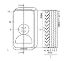
- (A) is a schematic external view of the electronic device of FIG. 1
- (b) is a cross-sectional view of (a) in the direction of line AA.
- the block diagram which shows the structural example of the image pickup part.
- the block diagram which shows the composition example by the sub-pixel of the image pickup part.
- the figure which shows the example of the photoelectric conversion element separation part Schematic perspective view of a wire grid polarizing element composed of a wire grid.
- a conceptual diagram for explaining light and the like passing through a wire grid polarizing element Schematic diagram of the configuration when the image pickup unit is a fingerprint sensor. The figure explaining the details of an optical characteristic such as a polarization state in an optical path. The figure explaining the details of an optical characteristic such as a polarization state in an optical path.
- a schematic configuration example of an electronic device which is an example of an image pickup device. Block diagram of the signal processing unit. The figure which shows the reflectance of the skin surface. The flowchart which shows the processing flow of the electronic device 1. Schematic cross-sectional view of an electronic device. Top view of the reflector. The schematic diagram in the case of constructing a polarizing plate in a fingerprint sensor.
- the figure which shows the cross-sectional structure of a pixel when a polarizing plate is formed in a fingerprint sensor The figure which shows the structural example of the polarizing plate which concerns on 2nd Embodiment.
- the schematic diagram in the case of further constructing a quarter wave plate in a fingerprint sensor.
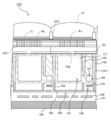
- FIG. 1A is a schematic cross-sectional view of the electronic device 1 according to the first embodiment.
- the electronic device 1 in FIG. 1A is an example of an electronic device 1 having an optical system, and is an arbitrary electronic device having both a display function and a shooting function, such as a smartphone, a mobile phone, a tablet, a barcode reader, and a PC, and is a module. It is equipped with a lens 9.
- FIG. 1B is a schematic cross-sectional view showing an example of an electronic device 1 having no module lens.
- the electronic device 1 of FIGS. 1A and 1B includes a camera module (imaging unit) arranged on the side opposite to the display surface of the display unit 2. As described above, the electronic device 1 of FIG. 1 is provided with the camera module 3 on the back side of the display surface of the display unit 2. Therefore, the camera module 3 shoots through the display unit 2.
- FIG. 2 (a) is a schematic external view of the electronic device 1 of FIG. 1
- FIG. 2 (b) is a cross-sectional view taken along the line AA of FIG. 2 (a).
- the display screen 1a extends close to the external size of the electronic device 1, and the width of the bezel 1b around the display screen 1a is set to several mm or less.
- a front camera is often mounted on the bezel 1b, but in FIG. 2A, as shown by a broken line, a camera module 3 that functions as a front camera on the back surface side of a substantially central portion of the display screen 1a. Is placed.
- the camera module 3 is arranged on the back surface side of the substantially central portion of the display screen 1a, but in the present embodiment, the camera module 3 may be on the back surface side of the display screen 1a, for example, the display screen 1a.
- the camera module 3 may be arranged on the back surface side near the peripheral portion of the camera module 3.
- the camera module 3 in the present embodiment is arranged at an arbitrary position on the back surface side overlapping with the display screen 1a.
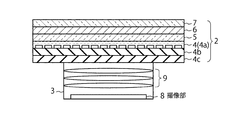
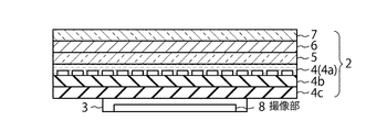
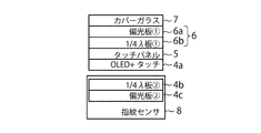
- the display unit 2 may include a polarizing plate 4c, a quarter wave plate 4b, a display panel 4 (4a), a touch panel 5, a circular polarizing plate 6, and a cover glass 7 (a touch panel may be included). ) Are stacked in order. Further, the circularly polarizing plate 6 has a polarizing plate 6a and a quarter wave plate 6b (see FIG. 9) as described later.
- the polarizing plate 4c and the quarter wave plate 4b suppress the internally reflected light from being incident on the camera module 3. Details of the polarizing plate 4c and the quarter wave plate 4b will be described later.
- the display panel 4 may be, for example, an organic light emitting diode (OLED: Organic Light Emitting Device), a liquid crystal display unit, a MicroLED, or a display panel based on other display principles.
- the display panel 4 such as the OLED unit is composed of a plurality of layers.
- the display panel 4 is often provided with a member having a low transmittance such as a color filter layer.
- a through hole may be formed in the member having a low transmittance in the display panel 4 according to the arrangement location of the camera module 3. If the subject light passing through the through hole is incident on the camera module 3, the image quality of the image captured by the camera module 3 can be improved.
- the circularly polarizing plate 6 is provided to reduce glare and improve the visibility of the display screen 1a even in a bright environment.
- a touch sensor is incorporated in the touch panel 5. There are various types of touch sensors such as a capacitance type and a resistance film type, and any method may be used. Further, the touch panel 5 and the display panel 4 may be integrated.
- the cover glass 7 is provided to protect the display panel 4 and the like.
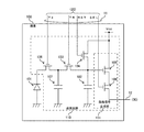
- FIG. 3 is a block diagram showing a configuration example of the imaging unit 8.
- the image pickup unit 8 includes a pixel array unit 10, a vertical drive unit 20, a column signal processing unit 30, and a control unit 40.
- the pixel array unit 10 has a plurality of pixels 100. That is, the plurality of pixels 100 are arranged in a two-dimensional grid pattern.
- the pixel 100 generates an image signal according to the irradiated light.
- the pixel 100 has a photoelectric conversion unit that generates an electric charge according to the irradiated light.
- the pixel 100 further has a pixel circuit. This pixel circuit generates an image signal based on the electric charge generated by the photoelectric conversion unit. The generation of the image signal is controlled by the control signal generated by the vertical drive unit 20 described later.
- the signal lines 11 and 12 are arranged in the pixel array unit 10 in an XY matrix.
- the signal line 11 is a signal line that transmits a control signal of the pixel circuit in the pixel 100, is arranged for each row of the pixel array unit 10, and is commonly wired to the pixel 100 arranged in each row.
- the signal line 12 is a signal line for transmitting an image signal generated by the pixel circuit of the pixel 100, is arranged for each row of the pixel array unit 10, and is commonly wired to the pixel 100 arranged in each row. To. These photoelectric conversion units and pixel circuits are formed on a semiconductor substrate.
- the vertical drive unit 20 generates a control signal for the pixel circuit of the pixel 100.
- the vertical drive unit 20 transmits the generated control signal to the pixel 100 via the signal line 11 in the figure.
- the column signal processing unit 30 processes the image signal generated by the pixel 100.
- the column signal processing unit 30 processes the image signal transmitted from the pixel 100 via the signal line 12 in the figure.
- the processing in the column signal processing unit 30 corresponds to, for example, analog-to-digital conversion for converting an analog image signal generated in the pixel 100 into a digital image signal.
- the image signal processed by the column signal processing unit 30 is output as an image signal of the image pickup device 1.
- the control unit 40 controls the entire image pickup unit 8.
- the control unit 40 generates a control signal for controlling the vertical drive unit 20 and the column signal processing unit 30, and controls the pixel (image sensor) 100.
- the control signal generated by the control unit 40 is transmitted to the vertical drive unit 20 and the column signal processing unit 30 by the signal lines 41 and 42, respectively.
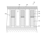
- FIG. 4 is a diagram showing an example of the cross-sectional structure of the pixel 100 shown in FIG. Pixels 100a and 100b show a side-by-side pixel example of the pixel array unit 10.
- an n-type semiconductor region is formed for each of the pixels 100a and 100b in, for example, a p-type semiconductor region of the semiconductor substrate 112.
- the photoelectric conversion element PD is formed in pixel units.
- a multilayer wiring layer composed of a transistor for reading out charges accumulated in the photoelectric conversion element PD and an interlayer insulating film is formed on the surface side (lower side in the figure) of the semiconductor substrate 112, a multilayer wiring layer composed of a transistor for reading out charges accumulated in the photoelectric conversion element PD and an interlayer insulating film is formed.
- An insulating layer 46 having a negative fixed charge is formed at the interface on the back surface side (upper side in the figure) of the semiconductor substrate 112.
- the insulating layer 46 is composed of a plurality of layers having different refractive indexes, for example, two layers of a hafnium oxide (HfO2) film 48 and a tantalum pentoxide (Ta2O5) film 47, and the insulating layer 46 is electrically pinned. By strengthening, it suppresses dark current and optically functions as an antireflection film.
- a silicon oxide film 49 is formed on the upper surface of the insulating layer 46, and a first light-shielding film portion 50 on which a pinhole 50a is formed is formed on the silicon oxide film 49.
- the first light-shielding film portion 50 may be a material that shields light from light, and is a material that has strong light-shielding properties and can be processed with high precision by fine processing, for example, etching. It is preferably formed of a titanium (Ti) or copper (Cu) film. Alternatively, they may be provided by an alloy thereof or a multilayer film of these metals.
- the first light-shielding film portion 50 forms a pinhole 50a and suppresses color mixing between pixels and light of a flare component incident at an unexpected angle.
- a light-shielding wall 61 and a plurality of layers of flattening films 62A and B having high light transmittance are formed in a plurality of stages. More specifically, the first light-shielding wall 61A is formed on a part of the first light-shielding film portion 50 between pixels, and the first flattening film 62A is formed between the first light-shielding walls 61A. It is formed. Further, a second light-shielding wall 61B and a second flattening film 62B are formed on the first light-shielding wall 61A and the first flattening film 62A.
- the light-shielding wall referred to here is provided with a metal such as tungsten (W), titanium (Ti), aluminum (Al), or copper (Cu), an alloy thereof, or a multilayer film of the metals. May be good.
- a metal such as tungsten (W), titanium (Ti), aluminum (Al), or copper (Cu), an alloy thereof, or a multilayer film of the metals. May be good.
- it may be provided with an organic light-shielding material such as carbon black.
- even if it is a transparent inorganic film it may have a structure that suppresses crosstalk by a total reflection phenomenon due to a difference in refractive index, and may have a shape in which the uppermost portion is closed as, for example, an Air Gap structure. In order to close the uppermost portion as the Air Gap structure, a film forming method having poor coverage, for example, sputtering can be used.
- a color filter 71 is formed for each pixel on the upper surfaces of the second light-shielding wall 61B and the second flattening film 62B.
- each color of R (red), G (green), and B (blue) is arranged by, for example, a Bayer arrangement, but may be arranged by another arrangement method.
- the image pickup unit 8 may be configured without arranging the color filter 71.
- the on-chip lens 72 is formed for each pixel on the color filter 71.
- the on-chip lens 72 may be made of an organic material such as a styrene resin, an acrylic resin, a styrene-acrylic copolymer resin, or a siloxane resin.
- the refractive index of the styrene resin is about 1.6, and the refractive index of the acrylic resin is about 1.5.
- the refractive index of the styrene-acrylic copolymer resin is about 1.5 to 1.6, and the refractive index of the siloxane resin is about 1.45.
- it may be composed of an inorganic material such as SiN or SiON.
- the refractive index of SiN is about 1.9, and SiON has a refractive index between SiN and the silicon oxide film.
- a filter layer that transmits a specific wavelength such as cyan, magenta, or yellow may be provided in addition to red, green, and blue.
- the color filter 71 is not only composed of an organic material-based color filter layer using an organic compound such as a pigment or a dye, but also a photonic crystal or a wavelength selection element applying plasmon (a lattice-shaped hole structure in a conductor thin film). It can also be composed of a color filter layer having a conductor lattice structure provided with the above (see, for example, Japanese Patent Application Laid-Open No. 2008-177191) and a thin film made of an inorganic material such as amorphous silicon.
- the inner lens 1210 is made of an inorganic material such as SiN or SiON.
- the inner lens 1210 is formed on the formed first-stage light-shielding wall layer (first light-shielding wall 61A and first flattening film 62A.
- the inner lens is provided to increase the focusing power and beam. The spot diameter of the waist can be reduced.
- the inner lens may be provided in a plurality of stages in one pixel, or the image pickup unit 8 may be configured without the inner lens. In the light-collecting design, it is desirable to align the light-collecting point with the pinhole 50a of the first light-shielding film portion 50.
- the structure shown in FIG. 4 is merely an example.
- a pinhole 50a is formed by a wiring layer of a surface-illuminated image pickup device, and an on-chip lens or an inner lens is provided so as to align a focusing point with the pinhole. May be good.
- a pinhole 50a may be formed of a light-shielding metal of a CCD (charge-coupled device) to prevent smear, and an on-chip lens or an inner lens may be provided so as to align a condensing point with the pinhole.
- CCD charge-coupled device
- FIG. 5 is a block diagram showing a configuration example of the subpixel 124 of the imaging unit 8. As shown in FIG. 5, the image pickup unit 8 is different from the image pickup unit 8 shown in FIG. 3 by reading a signal from the subpixel 124. Since the latter configuration is the same as that of the image pickup unit 8 shown in FIG. 3, the description thereof will be omitted.
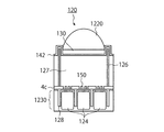
- FIG. 6A is a diagram showing an example of the configuration of the sub-pixel 124.
- the pixel 120 is a wiring composed of a semiconductor substrate 123, a plurality of subpixels 124, a plurality of photoelectric conversion element separation portions 128 provided between the subpixels 124, and an insulating layer and a wiring layer.
- a layer 129, a lens 1220, and a light-shielding wall 126 between pixels are further provided.
- a plurality of sub-pixels 124 are provided for one pixel 120.
- the subpixel 124 is, for example, a photodiode.
- the number of subpixels 124 is not limited to this, and may be more or less than 25 as long as the processing can be performed appropriately.
- the sub-pixels 124 are all shown as the same square, but the present invention is not limited to this, and the sub-pixels 124 may have an appropriate shape based on the information to be acquired according to various situations. Alternatively, a different filter may be used for each sub-pixel 124 provided in the pixel 100.
- FIG. 6A is an example of a back-illuminated image sensor.
- a light ray vertical light
- an oblique direction direction not parallel to the optical axis of the lens 1220.
- the case where the light rays (diagonal lights 1 and 2) are incident is shown.
- a bundle (solid line) of parallel light rays incident from the upper part of the lens 1220 is focused on the subpixel 124 located at the center.
- the bundle (dotted line) of the light rays incident in the diagonal direction is focused on the subpixel 124 which is not the center.
- the vertical optical axis of the lens 1220 is used as a reference, but this is not always the case. Not limited to this, it may be determined in which direction the light ray is incident on the sub-pixel 124 located at the center of the pixel 120 by a pupil correction technique or the like described later.
- the semiconductor substrate 123 for example, a silicon substrate, forms a semiconductor region portion of an element constituting a pixel circuit.
- the elements of the pixel circuit are formed in the well region formed on the semiconductor substrate 123.
- the semiconductor substrate 123 in the figure is composed of a p-type well region.
- the pixel 120 has a plurality of photoelectric change elements 124, and the sub-pixel 124 is composed of an n-type semiconductor region and a p-type well region around the n-type semiconductor region.
- photoelectric conversion occurs.
- the electric charge generated by this photoelectric conversion is converted into an image signal by a pixel circuit (not shown).
- the semiconductor substrate 123 is further formed with a semiconductor region portion of a vertical drive unit, a column signal processing unit, and a control unit.
- the wiring layer 129 connects the semiconductor elements in the pixels to each other.
- the wiring layer 129 is also used for connection with a circuit outside the pixel and constitutes a signal line.
- the wiring of the wiring layer 129 is made of, for example, a metal such as copper or aluminum to transmit an electric signal, and the insulating layer is, for example, silicon oxide to insulate between the wirings.
- these insulating layers and wirings are formed adjacent to the front surface side of the semiconductor substrate 123 to form the wiring layer 129.
- a support substrate (not shown) is arranged adjacent to the wiring layer 129.
- This support substrate is a substrate that supports the image pickup device, and improves the strength of the image pickup device at the time of manufacture.
- a logic circuit or the like may be mounted on the support board in advance, and the semiconductor board 123 and the circuit of the support board may be electrically connected to each other as a laminated type.
- FIG. 6B is a diagram showing an example of the photoelectric conversion element separation unit 128.
- the photoelectric conversion element separation unit 128 may be provided with a p-type well region 139. Further, a groove may be formed in the semiconductor substrate 123 so that the information regarding the light intensity is not propagated to the photoelectric conversion element of the adjacent subpixel (photoelectric conversion unit) 124, and the insulating film 141 may be provided in the groove. .. Further, a metal film 138 may be provided in addition to the insulating film 141. A film 140 having a negative fixed charge may be provided on the light receiving surface of the semiconductor substrate 123 and the trench side wall of the photoelectric conversion element separation portion 128.
- the negative fixed charge film 140 can be composed of, for example, an oxide containing at least one of hafnium, zirconium, aluminum, tantalum, and titanium, or a nitride.
- the insulating film 141 is made of, for example, silicon oxide or the like, and insulates the photoelectric conversion element of the subpixel 124 from the metal film 138.
- the metal film 138 has an opening in at least a part of the subpixel 124, and may be further embedded in the gap of the insulating film 141 in the trench portion of the photoelectric conversion element separation portion 128.
- the metal film 138 may be shielded from light so as to cover the black reference pixel region and the peripheral circuit region.
- the metal film 138 is a light-shielding material, for example, a metal film such as tungsten, aluminum, silver, gold, copper, platinum, molybdenum, chromium, titanium, nickel, iron and tellurium, a compound of these metals, or oxidation thereof. It can be composed of an article, or a nitride thereof, or an alloy thereof. Further, these materials may be combined as a multilayer film.
- the remaining width of the metal film 138 at the pixel 100 boundary is made thicker than the remaining width of the metal film 138 other than the pixel 100 boundary. You may prepare.
- the remaining width of the metal film 138 of the photoelectric conversion element separation portion 128 may be larger or thinner than the trench width formed on the semiconductor substrate 123.
- the former suppresses deterioration of dark current and white point characteristics, and improves angular resolution.
- the latter improves sensitivity.
- a part of the photoelectric conversion element separating portion 128 included in the pixel 100 is provided with the metal film 138 only in the gap of the insulating film 141 in the trench portion, and the metal film 138 is provided above the surface of the insulating film 141. It does not have to be.
- the interlayer film 127 is provided on the upper part of the metal film 138, and may be made of a transparent material such as silicon oxide, silicon nitride, or SiON.
- a transparent material such as silicon oxide, silicon nitride, or SiON.
- an organic material such as a styrene resin, an acrylic resin, a styrene-acrylic copolymer resin, or a sirosan resin may be used, and the lens 1220 is directly provided on the organic material. May be good.
- the light-shielding wall 126 may be provided so as to penetrate the interlayer film 127 at the boundary of the pixels 120. Stray light can be shielded by providing the light-shielding wall 126.
- the light-shielding wall 126 is made of a material having a light-shielding property, for example, a metal film such as tungsten, aluminum, silver, gold, copper, platinum, molybdenum, chromium, titanium, nickel, iron and tellurium, or a compound of these metals, or a compound thereof. It can be composed of oxides, or nitrides thereof, or alloys thereof. Further, it can also be configured as a multilayer film in which these materials are combined.
- the light-shielding wall 126 may be divided into multiple stages in the third direction. At the boundary of the pixel 100, these light-shielding walls 126 and the metal film 138 may be in continuous contact with each other.
- the color filter 130 uses, for example, a pigment or a dye as a material, transmits light of a desired wavelength, and can obtain spectral information of light from a subject.
- the color filter 130 may be provided, for example, on the interlayer film 127, or may be provided with an adhesion layer 142 that also serves as flattening between the interlayer film 127 and the color filter 130.
- the color filter 130 may be provided, for example, on the metal film 138, or may be provided with an adhesion layer that also serves as a flattening film between the metal film 138 and the color filter 130.
- the color filter 130 may be provided, for example, one for each subpixel 124, or they may be different for each subpixel 124. Alternatively, one color filter 130 may be provided for each pixel 100, and they may be different for each pixel 100. It is not necessary to provide a color filter with an emphasis on sensitivity and resolution.
- One lens 1220 is provided, for example, for each pixel 120.
- the lens 1220 may be composed of a plurality of laminated lenses.
- the lens can be made of an organic material such as a styrene resin, an acrylic resin, a styrene-acrylic copolymer resin, and a sirosan resin. It can also be made of an inorganic material such as silicon nitride or silicon oxynitride. Antireflection films having different refractive indexes may be provided on the lens surface. Further, a flattening film made of an organic material, for example, an acrylic resin may be provided under the lens material for the base step.
- a transparent inorganic material flattened by CMP or the like for example, silicon oxide may be provided.
- an image pickup device having a pinhole in a pixel or an image pickup device having a plurality of subpixels in a pixel has been described as an example. , It may be a surface irradiation type.
- an organic photoelectric conversion film may be used instead of the photoelectric conversion element by pn junction in the semiconductor substrate.
- sufficient space can be secured when using a module lens, it is possible to acquire a subject image with less blur even if the image pickup device does not have a pinhole or a sub-pixel by designing the module lens. Yes, it does not exclude these combinations.
- the quarter wave plates 4b, 6b function by shifting the phase between the two vertically polarized components of the light wave.
- Typical quarter wave plates 4b and 6b are birefringent crystals such as quartz and mica in which the direction of the optical axis and the film thickness T are determined.
- a normal axis having a refractive index of no and an abnormal axis having a refractive index of ne are obtained.
- the normal axis is perpendicular to the optical axis and the anomalous axis is parallel to the optical axis.
- the quarter wave plate has a phase difference ⁇ ( ⁇ ) of 90 degrees
- the wavelength ⁇ can be expressed by Eq. (2). As described above, there is a correspondence relationship of the equation (2) between the wavelength ⁇ and the film thickness T of the quarter wave plate.
- the quarter wave plates 4b and 6b according to the present embodiment are set to a thickness such that the optical path difference of the light transmitted through the normal axis and the abnormal axis is one quarter wavelength. More specifically, in the case of biophotographing, for example, fingerprint or vein imaging, the emission color is set in advance. For example, when only the portion of the display panel 4a corresponding to the green (G) is illuminated, the thickness of the wavelength ⁇ is set to correspond to 550 nm.
- the thickness should be set so that the wavelength ⁇ corresponds to 500 nm. This makes it possible to perform bioimaging with higher accuracy.
- the difference between the wavelength ⁇ represented by the equation (2) and the center of gravity of the emission spectrum at the corresponding portion of the display panel 4a is, for example, 0.05 um or less. This makes it possible to bring the phase difference ⁇ ( ⁇ ) generated in the quarter wave plate closer to the design wavelength, and the authentication accuracy is further improved.
- the quarter wave plates 4b and 6b can be mainly composed of three types: true zero order (True Zero Order), multiple order (Multiple Order), and compound zero order (Compound Zero Order).
- a true zero-order wave plate can be configured as a true zero-order wave plate because a predetermined retardation (phase difference) can be obtained at the 0th order at the design wavelength. It is made by processing the plate thickness of one birefringent material to be extremely thin so that a specific phase difference can be obtained at the 0th order. For example, if only the portion corresponding to the green filter (G) is to be illuminated, a quarter wave plate at 550 nm is manufactured.
- the stability of the phase difference obtained for wavelength shift, temperature change, or oblique incidence is superior to multi-order and compound zero-order.
- this thin plate thickness may be damaged during fixing to the device or handling, and the yield may decrease.
- N is a natural number and an even number.
- T1 / 60 0.25 + N.
- the above-mentioned disadvantages of the multi-order type can be improved. It will be possible.
- the optical axes of two birefringent materials of the same material manufactured in multi-order are arranged so as to be orthogonal to each other. That is, in the equations (1) and (2), n is a natural number and an even number. As a result, the phase difference shift amounts generated for each material cancel each other out, so that the wavelength dependence and the temperature dependence on the obtained retardation can be reduced. However, it may be difficult to improve the incident angle dependence.
- the thickness T1 of the quarter wave plates 4b and 6b is configured to be 0 or a natural number when 15 is subtracted from T1 and divided by 60.
- the thickness T2 of the quarter wave plates 4b, 6b is configured to be 0 or a natural number when 12.5 is subtracted from T2 and divided by 54.3.
- the polarizing plate 6a As the polarizing plate 6a, an absorption type polarizing filter, a reflection type polarizing filter, a crystal system, a multilayer film system, or the like can be used.
- a film of a suitable vinyl alcohol-based polymer such as polyvinyl alcohol and partially formalized polyvinyl alcohol is dyed and stretched with a dichroic substance such as iodine and a dichroic dye. It is composed of a film which has been subjected to appropriate treatment such as cross-linking treatment in an appropriate order and method.
- appropriate treatment such as cross-linking treatment in an appropriate order and method.
- the film is stretched in the longitudinal direction. Therefore, in the obtained linear polarizing element, the polarization absorbing axis parallel to the longitudinal direction of the linear polarizing element and the width of the linear polarizing element are used. A polarization transmission axis parallel to the direction is obtained.
- the crystalline polarizing element 150 can be configured by, for example, a photonic crystal.
- a photonic crystal is a structure having a periodicity of the wavelength order of light in the refractive index. By controlling the period and shape of this structure, the transmittance on the transmission axis and the reflectance on the absorption axis can be set.
- the polarizing element 150 of the multilayer film system is composed of, for example, a multilayer film made of at least two or more kinds of film materials having different refractive indexes.
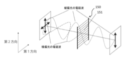
- FIG. 7 is a schematic perspective view of a so-called reflective wire grid polarizing element 150 configured by a wire grid.
- the polarizing element 150 in the figure represents an example of a polarizing element configured by a wire grid.
- the wire grid polarizing element 150 is a polarizing unit composed of strip-shaped conductors 151 arranged at a predetermined pitch. In the wire grid-shaped metal film, the polarized light in the direction (longitudinal direction) that the free electrons in the metal follow is canceled by the reflected wave, and the polarized light in the direction that does not follow (shortward direction) is transmitted.
- the pitch of the wire grid polarizing element is preferably less than 1/2 of the wavelength used, and if it exceeds this, diffracted light is generated.
- the band-shaped conductor 151 may be provided with the light reflecting layer 51 as a single layer, or the light absorbing layer 53 may be laminated on the light reflecting layer 51. Alternatively, an insulating layer 52 may be provided between the light reflecting layer 51 and the light absorbing layer 53.
- the constituent material of the light reflecting layer 51 is not particularly limited as long as it is a material having reflectivity to light in the band used, and for example, Al, Pt, Ag, Cu, Mo, Cr, Ti, Ni, W, and the like. Elemental substances such as Fe, Si, Ge, and Te, or alloys containing one or more of these elements can be mentioned. Above all, when the polarizing plate is used for visible light applications, the reflective layer is preferably made of aluminum or an aluminum alloy.
- silver (Ag), copper (Cu), gold (Au) or the like in order to give polarization characteristics to a wavelength band other than visible light, for example, an infrared region. This is because the resonance wavelengths of these metals are in the vicinity of the infrared region.
- an inorganic film or a resin film other than the metal formed with high reflectance on the surface by coloring or the like may be used.
- the reflected light from the wire grid polarizing element 150 may cause flare due to scattering inside the housing and cause deterioration of the image quality of the image pickup apparatus, or when strong light such as the sun is reflected on the display, the reflectance with the peripheral members. There is a concern that the difference may give a sense of discomfort in appearance.
- a light absorption layer 53 may be provided on the light reflection layer 51.
- the extinction coefficient k is not zero, that is, a metal material or alloy material having a light absorption action, a semiconductor material, specifically, tungsten (W), silver (Ag), or gold.
- Al copper
- Mo molybdenum
- Cr chromium
- Ti titanium
- Ni nickel
- Fe iron
- Si silicon
- Ge germanium
- Te tellurium
- metal materials such as (Sn), alloy materials containing these metals, and semiconductor materials.
- silicide-based materials such as FeSi2 (particularly ⁇ -FeSi2), MgSi2, NiSi2, BaSi2, CrSi2, and CoSi2 can also be mentioned.
- the light reflecting layer 51 and the light absorbing layer 53 are formed by various chemical vapor deposition methods (CVD method), coating method, various physical vapor deposition methods (PVD method) including sputtering method and vacuum vapor deposition method, and sol-gel method. , It can be formed based on a known method such as a plating method, a MOCVD method, or an MBE method.
- CVD method chemical vapor deposition methods
- PVD method physical vapor deposition methods
- sol-gel method sol-gel method.
- It can be formed based on a known method such as a plating method, a MOCVD method, or an MBE method.
- SiOX-based materials such as SiO2, NSG (non-doped silicate glass), BPSG (boron-phosphorus silicate-glass), PSG, BSG, PbSG, AsSG, SbSG, SOG (spin-on glass) (Constituent material), SiN, SiON, SiOC, SiOF, SiCN, low dielectric constant insulating material (for example, fluorocarbon, cycloperfluorocarbon polymer, benzocyclobutene, cyclic fluororesin, polytetrafluoroethylene, amorphous tetrafluoroethylene, polyaryl) Ether, Fluoroaryl Ether, Fluoropolymer, Organic SOG, Parylene, Fluorocarbon, Amorphous Carbon), Polypolymer Resin, Fluororesin,
- Insulation film material a trademark of Flare (Honeywell Electrical Materials Co.), and a polyaryl ether (PAE) -based material
- the insulating layer 52 can be formed based on known methods such as various CVD methods, coating methods, various PVD methods including sputtering methods and vacuum vapor deposition methods, various printing methods such as screen printing methods, and sol-gel methods.
- the insulating layer 52 functions as a base layer of the light absorbing layer, and at the same time, adjusts the phase of the polarized light reflected by the light absorbing layer and the polarized light transmitted through the light absorbing layer and reflected by the light reflecting layer to interfere with each other.
- the insulating layer 52 has a thickness such that the phase in one round trip is shifted by half a wavelength.
- the thickness of the insulating layer may be determined based on the balance between the desired polarization characteristics and the actual manufacturing process, for example, 1 ⁇ 10-9 m to 1 ⁇ 10-7 m, more preferably 1 ⁇ . 10-8m to 8 ⁇ 10-8m can be exemplified.
- the refractive index of the insulating layer is larger than 1.0 and is not limited, but is preferably 2.5 or less.
- an anisotropic dry etching technique using a combination of a lithography technique and an etching technique for example, carbon tetrafluoride gas, sulfur hexafluoride gas, trifluoromethane gas, xenon difluoride gas, etc.
- a lithography technique for example, carbon tetrafluoride gas, sulfur hexafluoride gas, trifluoromethane gas, xenon difluoride gas, etc.
- lithography technology photolithography technology (lithography technology using g-line, i-line, KrF excimer laser, ArF excimer laser, EUV, etc.
- the strip-shaped conductor 151 can be formed based on a microfabrication technique using an extremely short-time pulse laser such as a femtosecond laser or a nanoimprint method.
- a dielectric layer or both a dielectric layer and an air layer may be provided between the wire grids.
- the material constituting the dielectric layer is not particularly limited, but from the viewpoint of suppressing unnecessary reflection of light rays to be polarized in the polarizing plate, for example, Si oxide such as SiO2, AlF2, BaF2, CeF3, LaF3 , LiF, MgF2, NdF3, NaF, YF3 and the like.
- FIG. 8 is a conceptual diagram for explaining light and the like passing through the wire grid polarizing element.
- the extending direction (first direction) of the band-shaped conductor 151 coincides with the absorption axis for quenching, and the repeating direction of the band-shaped conductor 151 (which is the second direction and is orthogonal to the first direction) is the transmission axis for transmitting.
- Match That is, the free electrons in the band-shaped conductor 151 vibrate following the electric field of the light incident on the band-shaped conductor 151, and radiate the reflected wave.
- the light perpendicular to the longitudinal direction of the band-shaped conductor (second direction) reduces the radiation of the reflected light from the band-shaped conductor. This is because the vibration of free electrons is limited and the amplitude becomes small.
- the incident light on the transmission axis (second direction) is less attenuated by the polarizing element 150 and can pass through the polarizing element 150.
- the reflectance with respect to the incident light changes depending on the optical thickness of the light reflecting layer 51 (refractive index ⁇ film thickness of the light reflecting layer). Further, the reflectance with respect to the incident light also changes depending on the optical thickness of the light absorbing layer 53 (absorption rate ⁇ film thickness of the light reflecting layer).
- FIG. 9 is a schematic diagram of a configuration when the image pickup unit 8 is a fingerprint sensor.
- the light emitted from the display panel (OLED) 4a irradiates the fingerprint along the optical path L1 and is imaged by the fingerprint sensor 8. That is, the light emitted from the OLED 4a (display panel 4) irradiates the finger through the touch panel 5, the quarter wave plate 6b, the polarizing plate 6a, and the cover glass 7, and the scattered light from the finger is the cover glass. 7.
- the image is captured by the fingerprint sensor 8 via the polarizing plate 6a, the quarter wave plate 6b, the touch panel 5, the OLED 4a, the quarter wavelength plate 4b, and the polarizing plate 4c.
- a part of the light emitted from the OLED 4a is reflected by the polarizing plate 6a along the optical path L2, and further passes through the quarter wave plate 6b, the touch panel 5, the OLED 4a, and the quarter wave plate 4b.
- the polarizing plate 4c is irradiated and reflected by the polarizing plate 4c.
- the quarter wave plate 4b and the polarizing plate 4c are further provided to suppress the noise component reflected along the optical path L2 from being incident on the fingerprint sensor 8.
- FIG. 10 is a diagram illustrating details of optical characteristics such as polarization states in the optical paths L1 and L2.
- the absorption axis of the polarizing plate (1) can be arbitrarily provided, and the optical axis of the other optical members of FIG. 10 and FIG. 10 is defined relative to the polarizing plate (1).
- the transmission axis of the polarizing plate (1) is set to 0 degrees, and the sign of the angle is described by defining the clockwise direction in the + direction with respect to the traveling direction of light.
- the arrow at the bottom of FIG. 10 schematically shows the transmission axis.
- the transmission axis of the polarizing plate (1) that is, the polarized light set to 0 degrees is indicated by the up and down arrows, and the polarized light orthogonal to the polarizing plate (1) is indicated by the left and right arrows.
- FIG. 10 In the case of circularly polarized light, the traveling direction of light is unified toward the front of the paper surface, and the rotation direction of polarized light is indicated by an arc arrow. In the case of unpolarized light, it is shown that multiple arrows with different polarization directions are overwritten.
- the light emitted by the OLED 4a is applied to the fingerprint Fin via the touch panel 5, the quarter wave plate 6b, the polarizing plate 6a, and the cover glass 7.
- the slow axis of the quarter wave plate 6b is provided so as to be 45 ° (or 135 °).
- the transmission axis of the polarizing plate 6a is 0 degrees
- light with a polarization direction of 0 degrees is transmitted.
- the light scattered by the fingerprint Fin passes through the quarter wave plate 6b again as scattered light having a polarization direction of 0 degrees.
- the slow axis of the quarter wave plate 6b is 135 ° (or 45 °), and light with a polarization direction of 0 degrees is transmitted as circularly polarized light that rotates clockwise (or counterclockwise). do.
- the light transmitted through the quarter wave plate 6b further transmits through the touch panel 5 and the OLED 4a and is incident on the quarter wave plate 4b.
- the slow axis of the quarter wave plate 4b is provided to coincide with 6b.
- the traveling direction of the light it is 135 ° (or 45 °), so that the quarter wave plate 4b polarizes the incident light into linearly polarized light having a polarization direction of 90 degrees.
- the polarizing plate 4c is provided so that the absorption axis with the polarizing plate 6a is orthogonal to each other. Then, the 90-degree linearly polarized light transmitted through the quarter-wave plate 4b is transmitted through the polarizing plate 4c having a polarization direction of 90 degrees and is imaged by the fingerprint sensor 8.
- the noise light of the optical path L2 reflected by the polarizing plate 6a passes through the quarter wave plate 6b as polarized light in the 90-degree direction.
- the slow axis of the quarter wave plate 6b is 135 ° (or 45 °)
- light having a polarization direction of 90 degrees is transmitted as circularly polarized light that rotates counterclockwise (or clockwise).
- the light transmitted through the quarter wave plate 6b further transmits through the touch panel 5 and the OLED 4a and is incident on the quarter wave plate 4b.
- the slow axis of the quarter wave plate 4b is 135 ° (or 45 °), so the circularly polarized light of left-handed rotation (or right-handed rotation) is transmitted as linearly polarized light of 0 degree. ..
- the 0 degree linearly polarized light transmitted through the quarter wave plate 4b is reflected by the polarizing plate 4c having a polarization direction of 90 degrees and is not captured by the fingerprint sensor 8.
- the signal component from the fingerprint of the optical path L1 reaches the fingerprint sensor 8 and is imaged.
- the noise light of the optical path L2 reflected by the polarizing plate 6a is reflected by the polarizing plate 4c and cannot reach the fingerprint sensor 8.
- the signal component from the fingerprint can be imaged with the noise component reduced.
- a commercially available wire grid type polarizing plate has a reflectance of, for example, 50.6% for an unpolarized vertical incident, a transmittance of, for example, 45.3%, and a degree of polarization of transmitted light. Is 99.1 percent.
- the reflection component of the optical path L2 is 50.6%.
- the signal from the fingerprint is 41.0%, and the noise component due to the reflection of the polarizing plate 6a is 50.6%, that is, At an SN ratio of ⁇ 1.8 dB, the influence of noise becomes large. As a result, the identification accuracy is lowered.
- the quarter wave plate 4b and the polarizing plate 4c of the present embodiment are further provided and the above-mentioned wire grid type polarizing plate is used for the polarizing plate 4c
- a commercially available absorbent polarizing plate for example, a dichroic dye polarizing element
- a transmittance of, for example, 18.5% and the degree of polarization of transmitted light for unpolarized vertical incident. Is 99.1%.
- the reflection component of the optical path L2 is 5.1%.
- the signal from the fingerprint is 6
- the noise component due to the reflection of the polarizing plate 6a is 5.1% with respect to 0.8%, that is, the influence of noise is large at an SN ratio of 2.5 dB. As a result, the identification accuracy is lowered.
- the quarter-wave plate 4b and the polarizing plate 4c of the present embodiment are further provided, and the above-mentioned absorption-type polarizing plate is used for the polarizing plate 4c as the polarizing plate 4c.
- one of the polarizing plates 6a and 4c may be an absorption type and the other may be a wire grid type, and the combination is limited. It's not something to do.
- FIG. 11 is a diagram for explaining the details of optical characteristics such as the polarization state in the optical paths L1 and L2, and is provided so that the slow axes of the quarter wave plate 6b and 4b are orthogonal to each other, and the polarizing plate 6a, It differs from FIG. 10 in that the absorption axes of 4c are provided so as to coincide with each other.
- FIG. 11 FIG. 11
- the polarization component of the light emitted by the OLED 4a is evenly distributed in each direction.
- the light emitted by the OLED 4a is applied to the fingerprint Fin via the touch panel 5, the quarter wave plate 6b, the polarizing plate 6a, and the cover glass 7.
- the slow axis of the quarter wave plate 6b is provided so as to be 45 ° (or 135 °).
- the polarizing plate 6a Since the polarizing plate 6a has a polarization direction of 0 degrees, light having a polarization direction of 0 degrees is transmitted.
- the light scattered by the fingerprint Fin passes through the quarter wave plate 6b again as scattered light having a polarization direction of 0 degrees. Since the traveling direction of light is reversed, the slow axis of the quarter wave plate 6b is 135 ° (or 45 °), and light with a polarization direction of 0 degrees is transmitted as circularly polarized light that rotates clockwise (or counterclockwise). do.
- the light transmitted through the quarter wave plate 6b further transmits through the touch panel 5 and the OLED 4a and is incident on the quarter wave plate 4b.
- the slow axes of the quarter wave plate 4b are provided so as to be orthogonal to each other. Considering the traveling direction of the light, it is 135 ° (or 45 °), so that the quarter wave plate 4b polarizes the incident light into linearly polarized light having a polarization direction of 0 degree.
- the polarizing plate 4c is provided so that the absorption axis coincides with the polarizing plate 6a. Then, the linearly polarized light of 0 degree transmitted through the quarter wave plate 4b is transmitted through the polarizing plate 4c having a polarization direction of 0 degree and is imaged by the fingerprint sensor 8.
- the noise light of the optical path L2 reflected by the polarizing plate 6a passes through the quarter wave plate 6b as polarized light in the 90-degree direction.
- the slow axis of the quarter wave plate 6b is 135 ° (or 45 °)
- light having a polarization direction of 90 degrees is transmitted as circularly polarized light that rotates counterclockwise (or clockwise).
- the light transmitted through the quarter wave plate 6b further transmits through the touch panel 5 and the OLED 4a and is incident on the quarter wave plate 4b.
- the slow axis of the quarter wave plate 4b is 45 ° (or 135 °), so the circularly polarized light of left-handed rotation (or right-handed rotation) is transmitted as linearly polarized light of 90 degrees. ..
- the 90-degree linearly polarized light transmitted through the quarter-wave plate 4b is reflected by the polarizing plate 4c having a polarization direction of 0 degrees and is not captured by the fingerprint sensor 8.
- the signal component from the fingerprint of the optical path L1 reaches the fingerprint sensor 8 and is imaged.
- the noise light of the optical path L2 reflected by the polarizing plate 6a is reflected by the polarizing plate 4c and cannot reach the fingerprint sensor 8.
- the signal component from the fingerprint can be imaged with the noise component reduced.
- FIG. 12 is a block diagram showing a schematic configuration example of an electronic device 1 which is an example of an image pickup device to which the present technology can be applied.
- the electronic device 1 includes a display unit 2 (FIGS. 1A and 1B), an image pickup unit 8 (FIGS. 1A and 1B), a control unit 40 (FIG. 3), an operation input unit 1000, and a signal processing unit. It includes 1002, a storage unit 1004, an authentication unit 1006, and a result output unit 1008.
- the operation input unit 1000 receives an operation input from the user of the electronic device 1.
- the operation input unit 1000 is composed of, for example, a push button or a touch panel.
- the operation input received by the operation input unit 1000 is transmitted to the control unit 40 and the signal processing unit 1002. After that, processing according to the operation input, for example, processing such as fingerprint imaging is activated.
- control unit 40 sends a command to the image pickup unit to control the pixel array unit 10 (FIG. 3), sends a command to the display unit 2, and uses the light source of the display unit 2 to illuminate the subject. You can guess.
- the illumination light can change the balance of elements having different spectra of the display unit, for example, the three primary colors of red, blue, and green, and can change the light emitting area.
- a light source (not shown) other than the display unit 2 may be provided, and for example, light in an infrared region not included in the organic EL may be emitted. Infrared rays are suitable for acquiring vein information.
- the electronic device 1 is provided with the optical system 9 (FIG. 1A), autofocus can be performed.
- the autofocus is a system that detects the focal position of the optical system 9 and automatically adjusts it.
- this autofocus for example, a method of detecting the image plane phase difference by the phase difference pixels arranged in the image pickup unit 8 and detecting the focal position (image plane phase difference autofocus) can be used. It is also possible to apply a method (contrast autofocus) of detecting the position where the contrast of the image is highest as the focal position.
- the control unit 40 adjusts the position of the lens of the optical system 9 via the lens drive unit (not shown) based on the detected focal position, and performs autofocus.
- the control unit 40 can be configured by, for example, a DSP (Digital Signal Processor) equipped with firmware.
- DSP Digital Signal Processor
- the signal processing unit 1002 processes the image signal generated by the image pickup unit 8. This processing includes, for example, demosaic to generate an image signal of a color that is insufficient among the image signals corresponding to red, green, and blue for each pixel, noise reduction to remove noise of the image signal, addition processing of a plurality of pixels, and processing. Coding of image signals and the like are applicable.
- the signal processing unit 1002 can be configured by, for example, a microcomputer equipped with firmware.
- FIG. 13A is a block diagram of the signal processing unit 1002 according to the present embodiment.
- the signal processing unit 1002 includes an A / D conversion unit 502, a clamp unit 504, a color-coded output unit 506, a defect correction unit 508, a linear matrix unit 510, and a spectrum analysis unit 512. , And an image processing unit 518.
- the A / D conversion unit 502 (Analog to Digital Converter) converts the analog signal output from the image pickup unit 8 into a digital signal for each pixel.
- the clamp unit 504 executes, for example, a process relating to the level of the ground in the image.
- the clamp unit 504 defines, for example, a black level, and the defined black level is subtracted from the image data output from the A / D conversion unit 502 and output.
- the clamp unit 504 may set the ground level for each photoelectric conversion element provided in the pixel, and in this case, the ground correction of the signal value may be performed for each acquired photoelectric conversion element.
- the color-specific output unit 506 outputs the image data output from the clamp unit 504 for each color.
- the image pickup unit 8 is provided with R (red), G (green), and B (blue) filters in the pixel.
- the clamp unit 504 adjusts the ground level based on these filters, and the color-coded output unit 506 outputs the signal output by the clamp unit 504 for each color.
- the color-coded output unit 506 stores the data of the filter provided for each pixel in the image pickup unit 8. , You may output for each color based on this data.
- the image pickup unit 8 is provided with a color filter, but the present invention is not limited to this, and for example, an organic photoelectric conversion film may be used to identify colors.
- the defect correction unit 508 corrects defects in the image data. Defects in image data occur, for example, due to missing pixels or missing information due to defects in the photoelectric conversion element provided in the pixels, missing information due to saturation of light in the optical system 9, and the like.
- the defect correction unit 508 may execute the defect correction process by performing interpolation processing based on, for example, the information of the surrounding pixels or the received intensity of the peripheral photoelectric conversion element in the pixel.
- the linear matrix unit 510 performs correct color reproduction by executing a matrix operation on color information such as RGB.
- the linear matrix unit 510 is also referred to as a color matrix unit.
- the linear matrix unit 510 obtains a desired spectrum by, for example, performing an operation on a plurality of wavelengths.
- the linear matrix unit 510 performs an operation so as to output an output suitable for detecting skin color.
- the linear matrix unit 510 may be provided with a calculation path of a system different from that of the skin color, and may perform a calculation for acquiring vein information, for example.
- an operation may be performed so as to perform an output suitable for the vicinity of 760 nanometers.
- Veins are rich in reduced hemoglobin, which has a characteristic absorption spectrum near 760 nanometers.
- FIG. 13B is a diagram showing the reflectance of the skin surface.
- the vertical axis shows the reflectance, and the horizontal axis shows the wavelength.
- the skin color varies from individual to individual, but generally there is a rise in the wavelength region of 550 to 600 nanometers.
- the spectrum analysis unit 512 determines, for example, whether or not there is a rise in the spectrum peculiar to the skin, based on the data output by the linear matrix unit 510.
- the spectrum analysis unit 512 detects, for example, the rise of a signal of 550 to 600 nanometers in a range including 500 to 650 nanometers, so that the human finger is in contact with the cover glass 7, or in that case, the cover glass 7. It detects and outputs what the wavelength is.
- the range to be determined is not limited to the above range, and may be wider or narrower than this in an appropriate range. For example, it may be analyzed whether or not the reduced hemoglobin has a peak near 760 nanometers.
- the image processing unit 518 extracts the feature points of the fingerprint shape based on the image signal generated by the linear matrix unit 510. Further, the image processing unit 518 extracts the feature points of the veins based on the image signal generated by the linear matrix unit 510.
- the storage unit 1004 stores various data. The storage unit 1004 may store, for example, a frame which is an image signal for one screen, or may store data in the process of signal processing and authentication processing.
- the authentication unit 1006 executes personal authentication based on the data output by the signal processing unit 1002.
- the authentication unit 1006 executes personal authentication based on, for example, the rising wavelength analyzed by the spectrum analysis unit 512 and the fingerprint shape (feature point) based on the data output from the defect correction unit 508 or the like.
- the authentication unit 1006 may analyze the rhythm of the peak of the reduced hemoglobin near 760 nanometers, and if it is not rhythmic, it determines that the imaging target is an artificial object. In this way, the authentication unit 1006 can improve the biometric authentication accuracy by capturing the hemoglobin signal, that is, the rhythm of the heartbeat from the blood flow.
- Personal information may be stored in, for example, the authentication unit 1006 as a wavelength range, a fingerprint feature point, and a vein feature point, or may be stored in the storage unit 1004.
- the authentication unit 1006 can determine that the object is a finger and authenticate that the object is a memorized individual.
- the authentication unit 1006 acquires the shape characteristics of the fingerprint from the output from the image processing unit 518 and the like, and uses this information to determine whether or not the fingerprint matches the fingerprint to be authenticated. For example, the authentication unit 1006 determines whether or not the feature points of the fingerprint stored in the storage unit 1004 match the feature points of the authentication target.
- a general method can be used for fingerprint authentication.
- the authentication unit 1006 determines that the object in contact with the cover glass 7 is a living body by using this data.
- the authentication unit 1006 acquires the shape characteristics of the vein from the output from the image processing unit 518 and the like, and uses this information to determine whether or not the vein matches the vein to be authenticated. For example, the authentication unit 1006 authenticates whether or not the individual is a memorized individual by comparing a predetermined number of feature points extracted from the vein with the feature points stored in the storage unit 1004. A general method can be used for vein authentication.
- the result output unit 1008 outputs the personal authentication result based on the result output from the authentication unit 1006. For example, when the storage unit 1004 matches the recorded individual, the result output unit 1008 matches the recorded individual data when the finger in contact with the cover glass 7 at that timing matches the recorded individual data. , The authentication OK signal is output to the display unit 2, and in other cases, the authentication NG signal is output to the display unit 2.
- FIG. 14 is a flowchart showing a processing flow of the electronic device 1 according to the present embodiment. As an example, a case where the electronic device 1 performs personal authentication by a fingerprint, a spectrum, and a vein will be described.
- the electronic device 1 activates the image pickup unit 8 as a fingerprint sensor (S100).
- the above-mentioned components may be energized and put into a standby state.
- the electronic device 1 may explicitly activate the fingerprint sensor by a switch or the like.
- it may be obtained optically or mechanically that an object is in contact with the reading surface (cover glass) 7, and the fingerprint sensor may be activated by this acquisition as a trigger.
- the reading surface (cover glass) 7 may be triggered by detecting that the finger approaches a distance closer than a predetermined distance.
- the imaging unit 8 detects the intensity of the incident light at that timing, and acquires the condition of the external light based on this result (S102). For example, the electronic device 1 acquires an image in a state where light from the inside is not incident. By this acquisition, the intensity of sunlight, the intensity of light transmitted by the indoor light source through the finger, or the intensity of light entering through the gap between the fingers is detected. Based on this light intensity, the clamp portion 504 may perform ground processing in a later process.
- the light emitting portion provided in the electronic device 1 emits light so as to irradiate at least a part of the area where the finger and the cover glass 7 are in contact with each other (S104).
- the light emission may be white light or light having a specific wavelength, for example, light emission of R, G, B or the like.
- B (and G) may be emitted in order to obtain the surface shape.
- Infrared light may also be emitted to observe the veins.
- R may be emitted for spectral analysis. In this way, the light emission may emit an appropriate color based on the subsequent processing. These lights do not have to be emitted at the same timing. For example, R may be emitted first to acquire data for spectrum analysis, and then B and G may be emitted to acquire data for shape analysis.
- the image pickup unit 8 receives the light emitted by the display panel 4a including information such as fingerprints and reflected by the cover glass 7 (S106).
- the light receiving is executed by the image pickup unit 8 described above, and then necessary processing is executed. For example, following the light reception, processing of acquiring the shape of the fingerprint and acquiring the spectrum of reflected light or transmitted light is executed via A / D conversion and background correction.
- the authentication unit 1006 determines whether the shapes of the fingerprints match (S108).
- the determination of the shape of the fingerprint may be performed by a general method. For example, the authentication unit 1006 extracts a predetermined number of feature points from the fingerprint and compares the extracted feature points to determine whether or not it can be determined that the individual is a memorized individual.
- the authentication unit 1006 may make the light emitting region of the light emitting unit 4a emit light only in the corresponding region at the position where the finger (living body) is placed. As a result, it is possible to suppress the generation of noise light having various reflection angles caused by causing the display panel (light emitting unit) 4a to emit light in a wide range. Therefore, the authentication accuracy is further improved.
- the authentication unit 1006 subsequently determines whether or not the spectra match (S110).
- the authentication unit 1006 performs this determination by comparing the result of the spectrum analyzed by the spectrum analysis unit 512 with the result of the stored individual. For example, it is determined whether or not the acquired spectrum exists within an allowable range from the stored spectrum of the rise of the skin color. In this way, personal authentication may be performed not only by the fingerprint shape but also by the spectrum.
- the authentication unit 1006 subsequently determines whether or not the vein shapes match (S112).
- the authentication unit 1006 performs this determination by comparing the feature points of the vein shape with the feature points of the memorized individual. In this way, personal authentication may be performed not only by the fingerprint shape but also by the spectrum and the vein shape.
- the authentication unit 1006 determines that the authentication was successful (S114), and outputs the authentication result from the result output unit 1008.
- the result output unit 1008 outputs that the authentication is successful, and permits access to other configurations of the electronic device 1, for example.
- the output is performed when the result output unit 1008 is successful, but the output is not limited to this. Even in the cases of S108: NO, S110: NO, and S112: NO described above, the light emitting unit, the imaging unit 8, etc. are notified via the result output unit 1008 that the authentication has failed, and data acquisition is performed again. You may.
- the above is a process of repeating when authentication fails. For example, when the process is repeated a predetermined number of times, access to the electronic device 1 is blocked without performing further authentication. You may. In this case, the interface may prompt the user to enter another access means, for example, a passcode using the numeric keypad. Further, in such a case, since there is a possibility that the reading of the device has failed, the authentication process may be repeated while changing the light emission, the light receiving light, the state of the reading surface, the spectrum used, and the like. For example, when the analysis result that the product is wet is obtained, some output may be output to the user via the interface in order to wipe off the water and perform the authentication operation again.
- the quarter wave plate 4b and the polarizing plate 4c are provided.
- the signal component from the fingerprint of the optical path L1 reaches the fingerprint sensor 8 is imaged, and the noise light of the optical path L2 reflected by the polarizing plate 6a is reflected by the polarizing plate 4c and cannot reach the fingerprint sensor 8. Therefore, the S / N ratio is improved, and the authentication accuracy of the authentication unit 1006 is improved.
- the first embodiment is a modification of the first embodiment in that when light is incident from the cover glass 7, the reflectance of the region of the imaging unit 8 and the reflectance of the other region are configured to match. It differs from the form. Hereinafter, the differences from the first embodiment will be described.
- FIG. 15 is a schematic cross-sectional view of the electronic device 1 according to the modified example of the first embodiment.
- the electronic device 1 has parts such as a battery, a communication circuit, a microphone, and a speaker (not shown), and is often provided under the display unit 2.
- the position and shape of each component may be visually recognized by the user, which may give a sense of discomfort in appearance.
- an opaque cover portion 4d is provided on the back surface side of the display portion 2. By using the opaque cover portion 4d, the parts provided under the display portion 2 are not visually recognized by the user.
- the cover portion 4d is used as a reflector, not only the problem of appearance can be solved, but also the brightness of the display portion 2 can be increased by the contribution of the reflected light.
- the cover portion 4d is often made of a material mainly made of a metal such as copper or aluminum.
- the opaque cover unit 4d cannot be provided directly above the display unit 2, and a window unit 4e for transmitting light is required.
- the window portion 4e may give an appearance of discomfort.
- a circularly polarizing plate 6 is provided, but there is no perfect polarizing plate or a quarter wave plate, and variations such as film thickness and angle error at the time of mounting also affect external light reflection. Is difficult to make completely zero.
- the electronic device 1 when light is incident from the cover glass 7, it is reflected by the cover portion 4d shown in FIG. 15 and goes out of the cover glass. It is configured so that the difference in the amount of light between the emitted light L3 and the light L4 through which the light passing through the window portion 4e is reflected and passing through the outside of the cover glass is small.
- the cover portion 4d when the cover portion 4d is provided as a reflector and is mainly made of a metal such as copper or aluminum, the polarizing plate 4c is provided with a reflective type, for example, a wire grid polarizing element. If the cover portion 4d is mainly made of aluminum, the reflective layer of the wire grid is also mainly made of aluminum, and if the cover portion 4d is mainly made of copper, the reflective layer of the wire grid is also mainly made of copper. It is more desirable to prepare the material so that the spectra of the reflected light are aligned.
- the transmission axis of the polarizing plate 4c so as to coincide with the above-mentioned linearly polarized light. Be prepared for. That is, even if the main material of the reflective layer of the wire grid is aligned with the cover portion 4d, it is difficult to contribute to reducing the difference in the amount of light between the light L3 and the light L4 as it is. As a countermeasure, the width of the metal portion of the wire grid polarizing element may be widened in order to increase the reflection of polarized light on the transmission axis.
- the wire grid polarizing element of the polarizing plate 4c has a sufficient thickness, at least 300 nanometers or more, and the width of the metal part is at least 200 nanometers or more, preferably 300 nanometers or more. By doing so, the effect of suppressing the appearance visibility can be recognized.
- the polarizing plate 4c may be provided as an absorption type.
- the absorption type is a PVA film dyed and stretched with an iodine-based material or a dye-based material such as a dichroic dye.
- the polarizing plate 4c may be provided by a wire grid polarizing element 150 provided with a light absorbing layer. More specifically, from FIG. 7, for example, a wire grid polarizing element 150 in which a light absorption layer 53 in which antireflection tungsten is formed is formed on a light reflection layer 51 made of aluminum having high reflectance is configured. The reflectance may be balanced by controlling the film thickness. As described above, since the wire grid polarizing element 150 has the light reflecting layer 51 and the light absorbing layer 53, the reflectance can be adjusted by adjusting the thickness and material of each of the light reflecting layer 51 and the light absorbing layer 53. .. Alternatively, in the polarizing plate 4c, the difference in reflectance may be reduced by forming the image pickup unit 8 side with a reflective polarizing element and the display unit 2 side with an absorption type polarizing element.
- the orthogonal relationship with the polarizing plate 6a is broken, and the amount of light emitted from the cover glass 7 can be changed.
- the region corresponding to the window portion 4e may be hollowed out by the quarter wave plate 4b, and another quarter wave plate having the same outer shape but out of phase may be fitted.
- the angle at which the visibility of the window portion 4e is lost may be obtained by an experiment.
- the display unit 2 has the same light reflectance in the vertically upper region of the imaging unit 8 and the light reflectance in the other regions. It was decided to adjust the material, thickness, angle, or line width of the optical element included in. As a result, even if the incident light is incident through the cover glass 7, the amount of reflected light reflected through the cover glass 7 is made uniform.
- the electronic device 1 according to the second embodiment is different from the electronic device 1 according to the first embodiment in that the polarizing plate 4c is configured in the fingerprint sensor 8.
- the differences from the electronic device 1 according to the first embodiment will be described.
- FIG. 17 is a schematic diagram in the case where the image pickup unit 8 is configured with the polarizing plate 4c in the fingerprint sensor 8.
- the polarizing plate 4c is configured in the fingerprint sensor 8.
- the optical characteristics of the quarter wave plates 4b and 6b and the polarizing plates 4c and 6a can be made equivalent to the optical characteristics shown in FIG. 10 or FIG. That is, as shown in FIG. 10, the slow axis of the quarter wave plate 6b differs from the transmission axis of the polarizing plate 6a by 45 degrees or 135 degrees. Further, the transmission axis of the polarizing plate 6a and the transmission axis of the polarizing plate 4c are orthogonal to each other.
- the slow axis of the quarter wave plate 6b and the quarter wave plate 4b are the same.
- the slow axis of the quarter wave plate 6b differs from the transmission axis of the polarizing plate 6a by 45 degrees or 135 degrees.
- the transmission axis of the polarizing plate 6a and the transmission axis of the polarizing plate 4c are the same.
- the slow axes of the quarter wave plate 6b and the quarter wave plate 4b are orthogonal to each other.
- FIG. 18 is a diagram showing an example of the cross-sectional structure of the pixel 100 when the image pickup unit 8 constitutes the polarizing plate 4c in the fingerprint sensor 8.
- the pixel 100 includes a polarizing plate 4c, a base insulating layer 46, a first light-shielding film portion 50, a bank portion 61C, a color filter 71, an on-chip lens 72, and a semiconductor substrate 1201.
- a separation region 140, a flattening film 183, an insulating layer 191, a wiring layer 192, and a support substrate 199 are provided.
- the insulating layer 191 and the wiring layer 192 form a wiring region.
- a first light-shielding film portion 50 having a pinhole 50a is formed on the photoelectric conversion portion (light receiving region) 101.
- the first light-shielding film unit 50 described above shields the charge holding unit 107, which will be described later, from light-shielding.
- a base insulating layer 46 having a flattening layer as a lower layer is formed on the first light-shielding film portion 50, and a polarizing plate 4c having a wire grid polarizing element 150, a color filter 71, and an on-chip lens 72 are formed on the base insulating layer 46. Will be done.
- the bank portion 61C is configured to include, for example, a metal film. It is possible to dam the lens material with the bank portion 61C by the reflow process when forming the reflow lens. For example, in the reflow process, the material of the reflow lens 72 is dammed over the entire area of the bank portion 61C, and the shape of the reflow lens 72 is stabilized.
- the semiconductor substrate 1201 is a substrate on which the semiconductor portion of the element constituting the pixel circuit is formed.
- the semiconductor portion of the device is formed in a well region formed on the semiconductor substrate 1201.
- the semiconductor substrate 1201 in the figure is configured in a p-shaped well region.
- the semiconductor portion of the element is formed.
- the n-type semiconductor region 121 constitutes a photoelectric conversion unit 101. More specifically, the photoelectric conversion unit 101 is configured by a photodiode composed of a pn junction at the interface between the n-type semiconductor region 121 and the p-type well region around the n-type semiconductor region 121. The electric charge generated by the photoelectric conversion is accumulated in the n-type semiconductor region 121.
- the n-type semiconductor region 122 constitutes a floating diffusion type charge holding unit 107.
- a MOS transistor 108 is arranged between the n-type semiconductor regions 121 and 122.
- the MOS transistor 108 has n-type semiconductor regions 121 and 122 as sources and drains, respectively, and a p-type well region between them as a channel.
- the gate 135 is arranged adjacent to the channel of the MOS transistor 108.
- the insulating layer 191 between the semiconductor substrate 1201 and the gate 135 corresponds to the gate insulating film.
- the semiconductor substrate 1201 can be configured to have a thickness of, for example, 3 ⁇ m. Further, a p-type semiconductor region for pinning can be arranged in the vicinity of the front surface of the back surface of the semiconductor substrate 1201. This makes it possible to reduce noise based on the interface state.
- a wiring region composed of a wiring layer 192 and an insulating layer 191 described later is arranged on the surface side of the semiconductor substrate 1201.
- a fixed charge film 1410 (not shown) for strengthening the above-mentioned pinning and an oxide film 142 (not shown) for protecting and insulating the semiconductor substrate 1201 are arranged on the back surface side of the semiconductor substrate 1201.
- the fixed charge film 1410 may be composed of, for example, an oxide or a nitride containing at least one of hafnium (Hf), aluminum (Al), zirconium (Zr), tantalum (Ta) and titanium (Ti). can. Further, the fixed charge film 1410 can be formed by vapor deposition (CVD), sputtering and atomic layer deposition (ALD). When ALD is adopted, it is possible to simultaneously form a SiO 2 film that reduces the interface state during the film formation of the fixed charge film 1410, which is preferable.
- ALD atomic layer deposition
- the fixed charge film 1410 may be made of hafnium oxynitride or aluminum oxynitride. Alternatively, silicon (Si) or nitrogen (N) may be added to the fixed charge film 1410 in an amount that does not impair the insulating property. Thereby, heat resistance and the like can be improved.
- the oxide film 142 may be composed of, for example, SiO 2. It is formed by ALD to a thickness of 100 nm or less, more preferably 30 to 60 nm.
- the wiring layer 192 is a conductor for wiring an element formed on the semiconductor substrate 1201.
- the wiring layer 192 is made of a metal such as Cu.
- the insulating layer 191 insulates the wiring layer 192.
- the insulating layer 191 can be made of an insulating material, for example, SiO 2 .
- the wiring layer 192 and the insulating layer 191 can be configured in multiple layers.
- the separation region 140 is an region that separates the photoelectric conversion unit 101 of the adjacent pixels 100.
- the separation region 140 is arranged near the boundary between the pixels 100, and the inflow of electric charges from the adjacent pixels 100 can be prevented by injecting the ion implanter. Further, by forming a trench in the separation region 140 and embedding insulating films having different refractive indexes, it is possible not only to prevent the inflow of electric charges but also to block light obliquely incident from the adjacent pixels 100.
- the trench is formed in the separation region 140, it may be processed from the back surface side to the front surface side of the semiconductor substrate 1201, and further, it may be processed so as to penetrate the semiconductor substrate 1201.
- the separation region 140 may be made of a material that shields light from the gap, for example, metal. More specifically, Al, silver (Ag), gold (Ag), copper (Cu), platinum (Pt), molybdenum (Mo), chromium (Cr), Ti, nickel (Ni), W, iron (Fe). And can be composed of alloys containing tellurium (Te) and the like and these metals. Further, a plurality of these materials can be laminated and configured. Further, Ti, titanium nitride (TiN), and a film in which these are laminated can be arranged as an adhesion layer between the oxide film 142 and the oxide film 142.
- the sensitivity of the pixel 100 can be improved, which is preferable. This is because Al has a relatively high reflectance, and the light transmitted through the photoelectric conversion unit 101 (n-type semiconductor region 121) and incident on the separation region 140 is reflected and returned to the photoelectric conversion unit 101.
- the separation region 140 by Al can be formed by a known method, for example, high temperature sputtering.
- the groove for arranging the separation region 140 can be formed, for example, by dry etching the semiconductor substrate 1201. By embedding the above-mentioned insulating film or metal material in this groove, the separation region 140 can be arranged. This can be done, for example, by PVD (Physical Vapor Deposition) such as sputtering or vacuum vapor deposition, CVD, plating and coating methods.
- PVD Physical Vapor Deposition
- the second separation region 143 is a separation region arranged between the photoelectric conversion unit 101 and the second charge holding unit 107.
- the second separation region 143 is arranged in the groove formed in the semiconductor substrate 1201. Unlike the separation region 140, the groove in which the second separation region 143 is formed does not penetrate the semiconductor substrate 1201, and the bottom portion is formed at a relatively shallow position on the surface side of the semiconductor substrate 1201. Therefore, an opening is formed between the bottom of the second separation region 143 and the surface of the semiconductor substrate 1201, and the channel of the MOS transistor 108 is formed in the opening.
- the charge holding unit 107 holds a charge during the period from the end of the exposure period to the output of the image signal. During this holding period, for example, the photoelectric conversion unit 101 starts exposure of the next frame. At this time, when the electric charge flows from the photoelectric conversion unit 101 to the second charge holding unit 107, the image signals of different frames are mixed as noise. Therefore, by arranging the second light-shielding region 143 between the photoelectric conversion unit 101 and the second charge holding unit 107 except for the channel region of the MOS transistor 108, the inflow of electric charge can be suppressed and noise can be suppressed. Mixing can be reduced. Further, by arranging the second light-shielding region 143, the light incident on the second charge holding unit 107 from the region of the photoelectric conversion unit 101 can be shielded, and the mixing of noise based on the incident light can be reduced. Can be done.
- the lid portion 195 is arranged on the insulating layer 191 in the wiring region and shields the incident light transmitted through the photoelectric conversion portion 101.
- the lid portion 195 is composed of a wall portion 194 and a bottom portion 193.
- the lid portion 195 covers the space between the photoelectric conversion unit 101 and the wiring layer 192 in a lid shape to block light. A part of the light incident on the pixel 100 is transmitted without contributing to the photoelectric conversion in the photoelectric conversion unit 101. When this transmitted light is reflected by the wiring layer 192 in the wiring region and is incident on the photoelectric conversion unit 101 of the other pixel 100, noise is mixed in the other pixel 100 and the image quality is deteriorated.
- the wall portion 194 and the bottom portion 193 may be made of a metal such as Cu as in the wiring layer 192.
- the separation region 140 and the second separation region 143 are configured by arranging a material such as W or Al in the groove formed in the semiconductor substrate 1201.
- the groove in which the separation region 140 is arranged is formed deeper than the groove in which the second separation region 143 is arranged. This can be done, for example, by forming a two-step groove. First, the semiconductor substrate 1201 is etched to form a groove having a depth corresponding to the second separation region 143 at a position where the separation region 140 and the second separation region 143 are formed. Next, the groove in which the second separation region 143 is arranged is protected by a resist or the like, and the groove in which the separation region 140 is arranged is etched again. This allows grooves of different depths to be formed.
- a film of a material constituting the separation region 140, the second separation region 143, and the polarizing element 150, for example, a film of W or Al is formed on the semiconductor substrate 1201 and arranged in these grooves.
- the metal film contained in the bank portion 61C can effectively suppress stray light from the gap portion. Further, since the wire grid polarizing element 150 can be provided close to the photoelectric conversion unit 101, it is possible to prevent light leakage (polarization crosstalk) to the adjacent image pickup element.
- FIG. 19 is a diagram showing a configuration example of the polarizing plate 4c according to the present embodiment.
- the polarizing plate 4c is composed of an adhesion layer 167, a side wall protective layer 165, an upper protective layer 166, and a void 169.
- the adhesion layer 167 is arranged between the base insulating layer 46 and the light reflection layer 51 to improve the adhesion strength of the light reflection layer 51.
- the adhesion layer 167 for example, Ti, TiN and a film in which these are laminated are used.
- a gas such as air is sealed in the gap 169 between the band-shaped conductors 151.
- the transmittance of the polarizing plate 4c can be improved. This is because air and the like have a refractive index of about 1.
- the side wall protective layer 165 is arranged around the strip-shaped conductor 151 formed by the laminated light reflecting layer 51, the insulating layer 52, and the light absorbing layer 53, and mainly protects the side wall of the strip-shaped conductor 151.
- the metal material or alloy material constituting the light reflecting layer 51 and the light absorbing layer 53 comes into contact with air (outside air).
- the side wall protective layer 165 By arranging the side wall protective layer 165, it is possible to prevent corrosion and deterioration of the light reflecting layer 51 and the like due to moisture in the outside air and the like.
- a material having a refractive index of 2 or less and an extinction coefficient close to zero is adopted for the side wall protective layer 165.
- the side wall protective layer 165 is made of an insulating material made of Si such as SiO 2 , SiON, SiN, SiC, SiOC and SiCN. Further, the side wall protective layer 165 may be composed of a metal oxide such as aluminum oxide (AlOx), hafnium oxide (HfOx), zirconium oxide (ZrOx) and tantalum oxide (TaOx).
- AlOx aluminum oxide
- HfOx hafnium oxide
- ZrOx zirconium oxide
- TaOx tantalum oxide
- the side wall protective layer 165 can be formed by using these materials and forming a film by a known method such as CVD, PVD, ALD and a sol-gel method.
- the upper protective layer 166 is a film that is arranged adjacent to the upper surface of the strip-shaped conductor 151 and closes the gap 169.
- the upper protective layer 166 is made of the same material as the side wall protective layer 165 described above. Further, the upper protective layer 166 can be formed by a film forming method in which the material is not deposited in the void 169 but is deposited on the upper surface of the band-shaped conductor 161, for example, PVD.
- the light reflecting layer 51, the insulating layer 52, and the light absorbing layer 53 are configured to have thicknesses of, for example, 150 nm, 25 nm, and 25 nm, respectively.
- the polarizing element 150 By arranging the polarizing element 150 having such a multilayer structure, the reflected light from the polarizing element 150 is reduced. Further, it is possible to improve the transmittance by using a polarizing plate 4c having an air gap structure. By arranging the polarizing plate 4c having a three-layer structure in this way, the reflection from the polarizing plate 4c can be reduced.
- FIG. 20 is a diagram showing an example of the circuit configuration of the pixel 100 according to the second embodiment.
- the pixel 100 includes a photoelectric conversion unit 101, a charge holding unit 102, a second charge holding unit 107, and MOS transistors 103 to 108.
- the cathode of the photoelectric conversion unit 101 is connected to the source of the MOS transistor 108, and the gate of the MOS transistor 108 is connected to the transfer signal line TX.
- the drain of the MOS transistor 108 is connected to the source of the MOS transistor 103 and one end of the second charge holding portion 107. The other end of the second charge holding portion 107 is grounded.
- the drain of the MOS transistor 103 is connected to the source of the MOS transistor 104, the gate of the MOS transistor 105, and one end of the charge holding portion 102. The other end of the charge holding portion 102 is grounded.
- the drain of the MOS transistors 104 and 105 is commonly connected to the power line Vdd, and the source of the MOS transistor 105 is connected to the drain of the MOS transistor 106.
- the source of the MOS transistor 106 is connected to the signal line 12.
- the gates of the MOS transistors 103, 104 and 106 are connected to the transfer signal line TR, the reset signal line RST and the selection signal line SEL, respectively.
- the transfer signal line TR, the reset signal line RST, and the selection signal line SEL constitute the signal line 11.
- the photoelectric conversion unit 101 generates an electric charge according to the irradiated light as described above.
- a photodiode can be used for the photoelectric conversion unit 101.
- the charge holding units 102 and 107 and the MOS transistors 103 to 108 form a pixel circuit.
- the MOS transistor 103 is a transistor that transfers the electric charge generated by the photoelectric conversion of the photoelectric conversion unit 101 to the charge holding unit 102.
- the charge transfer in the MOS transistor 103 is controlled by the signal transmitted by the transfer signal line TR.
- the charge holding unit 102 is a capacitor that holds the charge transferred by the MOS transistor 103.
- the MOS transistor 105 is a transistor that generates a signal based on the charge held in the charge holding unit 102.
- the MOS transistor 106 is a transistor that outputs a signal generated by the MOS transistor 105 to the signal line 12 as an image signal.
- the MOS transistor 106 is controlled by a signal transmitted by the selection signal line SEL.
- the MOS transistor 104 is a transistor that resets the charge holding unit 102 by discharging the charge held by the charge holding unit 102 to the power supply line Vdd.
- the reset by the MOS transistor 104 is controlled by the signal transmitted by the reset signal line RST, and is executed before the charge transfer by the MOS transistor 103.
- the photoelectric conversion unit 101 can also be reset by conducting the MOS transistor 103. In this way, the pixel circuit converts the electric charge generated by the photoelectric conversion unit 101 into an image signal.
- the MOS transistors 105 and 106 form the image signal generation unit 111.
- the second charge holding unit 107 holds the charge generated by the photoelectric conversion unit 101.
- the second charge holding unit 107 holds the charge during the period from the end of the exposure on the pixel 100 to the start of the output of the image signal.
- the MOS transistor 108 is a transistor that transfers the electric charge generated by the photoelectric conversion unit 101 to the second charge holding unit 107.
- the image pickup element 1 in which the pixel 100 provided with the pixel circuit of the figure is arranged can be imaged as follows. First, the MOS transistors 103, 104 and 108 are made conductive to reset the photoelectric conversion unit 101, the charge holding unit 102 and the second charge holding unit 107. This reset is performed simultaneously in all the pixels 100 arranged in the pixel array unit 10. Next, the MOS transistors 103, 104 and 108 are transitioned to the non-conducting state. This starts the exposure period. After the elapse of the predetermined exposure period, the MOS transistors 103 and 104 are conducted again to reset the second charge holding unit 107, and then the MOS transistor 108 is conducted to conduct the charge generated by the photoelectric conversion unit 101 to the second charge. Transfer to the charge holding unit 107. As a result, the exposure period of all the pixels 100 is stopped at the same time.
- the MOS transistor 104 is made conductive to reset the charge holding unit 102 again, and the MOS transistor 103 is made conductive to transfer the charge of the second charge holding unit 107 to the charge holding unit 102.
- the MOS transistor 106 is made conductive and the image signal generated by the MOS transistor 105 is output to the signal line 12.
- the processing from the reset of the charge holding unit 102 to the output of the image signal is executed row by row from the first row of the pixel array unit 10.
- the image signal of one frame can be output from the pixel 100.
- the exposure and the output of the image signal are executed at intervals. Can be done. It is possible to simultaneously expose all the pixels 100 arranged in the pixel array unit 10.
- Such an imaging format is called a global shutter format. Further, after the charge is transferred to the second charge holding unit 107, the exposure of the next frame can be started.
- FIG. 21 is a schematic diagram in the case where the polarizing plate 4c is configured in the pinhole 50a of the first light-shielding film portion 50.
- the polarizing plate 4c is different from the electronic device 1 shown in FIG. 18 in that the polarizing plate 4c is configured in the pinhole 50a.
- FIG. 22 is a schematic diagram in the case where the polarizing plate 4c is configured in the pixel 120.
- the pixel 120 is provided with an on-chip lens 1220, a color filter 130 is provided under the on-chip lens 12, and a polarizing plate 4c is provided with a light-shielding wall 126 for suppressing crosstalk interposed therebetween.
- the light polarized by the polarizing plate 4c can be imaged for each subpixel 124.
- FIG. 23 is a block diagram showing a schematic configuration example of an electronic device 1 which is an example of an image pickup device to which the present technology can be applied.
- the electronic device 1 includes a display unit 2 (FIGS. 1A and 1B), an image pickup unit 8 (FIGS. 1A and 1B), a control unit 40 (FIG. 3), an operation input unit 1000, and a signal processing unit. It includes 1002, an authentication unit 1010, a result output unit 1008, and a storage unit 1004.
- the authentication unit 1010 has a so-called barcode reader function that further authenticates the geometric shape in addition to the authentication function of the authentication unit 1006 according to the first embodiment.
- the electronic device 1 does not cause a shift in the exposure period for each pixel row, so that distortion during imaging of a moving subject can be reduced. Therefore, the authentication unit 1006 can perform authentication while moving the subject or the electronic device 1 and performing a scanning operation in the authentication of the learning shape.
- the authentication unit 1006 can perform authentication while moving the subject or the electronic device 1 and performing a scanning operation. That is, in biometric authentication, the authentication unit 1006 can perform authentication by flipping the living body without resting.
- the polarizing plate 4c is arranged in the pixel 100 (120).
- the polarized light is polarized in the pixel 100 (120), and the polarized light can be imaged by the photoelectric conversion unit 101 (124).
- the wire grid polarizing element 150 can be provided close to the photoelectric conversion unit 101 (124), it is possible to prevent light leakage (polarization crosstalk) to the adjacent photoelectric conversion unit 101 (124). ..
- the electronic device 1 according to the third embodiment is different from the electronic device 1 according to the second embodiment in that the quarter wave plate 4b is further configured in the fingerprint sensor 8.
- the differences from the electronic device 1 according to the second embodiment will be described.
- FIG. 24 is a schematic diagram in the case where the quarter wave plate 4b is further configured in the fingerprint sensor 8.
- the quarter wave plate 4b and the polarizing plate 4c are configured in the fingerprint sensor 8.
- the optical characteristics of the quarter wave plates 4b and 6b and the polarizing plates 4c and 6a can be made equivalent to the optical characteristics shown in FIG. 10 or FIG. That is, as shown in FIG. 10, the slow axis of the quarter wave plate 6b differs from the transmission axis of the polarizing plate 6a by 45 degrees or 135 degrees. Further, the transmission axis of the polarizing plate 6a and the transmission axis of the polarizing plate 6a are orthogonal to each other.
- the slow axis of the quarter wave plate 6b and the quarter wave plate 4b are the same.
- the slow phase of the quarter wave plate 6b differs from the transmission axis of the polarizing plate 6a by 45 degrees or 135 degrees.
- the transmission axis of the polarizing plate 6a and the transmission axis of the polarizing plate 6a are the same.
- the slow axes of the quarter wave plate 6b and the quarter wave plate 4b differ by 90 degrees.
- FIG. 25 is a diagram showing a cross-sectional structure of a pixel 100 when a quarter wave plate 4b is further configured in the fingerprint sensor 8. As shown in FIG. 23, the pixel 100 has a quarter wave plate 4b laminated under the color filter 71. As a result, the light that is linearly polarized in the pixel 100 and polarized light can be imaged by the photoelectric conversion unit 101.
- FIG. 26 is a schematic diagram in the case where the quarter wave plate 4b and the polarizing plate 4c are configured in the pinhole 50a of the first light-shielding film portion 50.
- the electronic device 1 shown in FIG. 20 includes the quarter wave plate 4b, and the polarizing plate 4c is configured in the pinhole 50a, which is different from that of the electronic device 1 shown in FIG. It's different.
- the quarter wave plate 4b and the polarizing plate 4c By providing the quarter wave plate 4b and the polarizing plate 4c in this way, linearly polarized light can be captured by the photoelectric conversion unit 101. Further, since the quarter wave plate 4b and the polarizing plate 4c are provided in the image pickup apparatus, it is possible to reduce the thickness and size of the region that was the quarter wavelength plate 4b and the polarizing plate 4c.
- FIG. 27 is a schematic diagram in the case where the quarter wave plate 4b and the polarizing plate 4c are configured in the pixel 120.
- the pixel 120 is provided with an on-chip lens 1220, a color filter 130 is provided under the pixel 120, and a polarizing plate 4c is provided with a light-shielding wall 126 for suppressing crosstalk interposed therebetween.
- a quarter wave plate 4b is provided above the polarizing plate 4c. As a result, the polarized light can be imaged by linearly polarized light for each subpixel 124.
- the quarter wave plate 4b and the polarizing plate 4c are arranged in the pixel 100 (120).
- the light is linearly polarized in the pixel 100 (120) and the polarized light can be imaged by the photoelectric conversion unit 101 (124).
- the present technology can have the following configurations.
- the first polarizing plate that converts the incident light into linearly polarized light A first quarter wave plate whose slow axis differs from the absorption axis of the first polarizing plate by 45 degrees or 135 degrees. Self-luminous element layer and The first quarter wave plate and the second quarter wave plate having the same direction of the slow axis as the first quarter wave plate.
- the first polarizing plate that converts the incident light into linearly polarized light A first quarter wave plate whose slow axis differs from the absorption axis of the first polarizing plate by 45 degrees or 135 degrees.
- the self-luminous element layer is a display having a self-luminous element.
- the image pickup device is an image pickup device that captures the scattered light of a finger irradiated with the light of the self-luminous element through the first quarter wave plate and the first polarizing plate.
- the scattered light of the finger is the first polarizing plate, the first quarter wave plate, the self-luminous element layer, the second quarter wave plate, and the second polarizing plate.
- the electronic device according to (1) or (2), further comprising.
- the image pickup device is an image pickup device that captures an image of an authentication target irradiated with light from the self-luminous element via the first quarter wave plate and the first polarizing plate. Light from the certification target passes through the first polarizing plate, the first quarter wave plate, the self-luminous element layer, the second quarter wave plate, and the second polarizing plate. Imaged, The image pickup device outputs an image signal based on incident light incident through optical members having different wavelength transmission characteristics. 4.
- the image pickup device is an image pickup device that captures an image of an authentication target irradiated with light from the self-luminous element via the first quarter wave plate and the first polarizing plate. Light from the certification target passes through the first polarizing plate, the first quarter wave plate, the self-luminous element layer, the second quarter wavelength plate, and the second polarizing plate.
- Imaged as a vein image A signal processing unit that extracts feature points from the vein image, A storage unit that stores the feature points of the vein to be authenticated, An authentication unit that collates the feature points extracted from the vein image with the feature points of the vein to be authenticated and determines whether or not they match.
- the electronic device according to (1) or (2).
- the image pickup device is On-chip lens and A metal light-shielding film portion having a pinhole corresponding to the position where the on-chip lens collects light,
- the image pickup device is A metal wire grid polarizing element is placed in the pinhole.
- the image pickup apparatus has a pixel array composed of a plurality of pixels.
- the pixel is A plurality of sub-pixels having a photoelectric conversion element that receives light incident at a predetermined angle and outputs an analog signal based on the intensity of the received light.
- An on-chip lens that concentrates the incident light on the sub-pixels, The electronic device according to (1) or (2).
- the wire grid polarizing element is a structure in which a light reflecting layer made of a first conductive material and a light absorbing layer made of a second conductive material are laminated above the reflection layer (12).
- the image pickup device has a color filter in the pixel, and the image pickup device has a color filter.
- the second polarizing plate includes a reflection type polarizing filter, an absorption type polarizing filter, and the like.
- the second polarizing plate has a wire grid polarizing element.
- the electron according to (1) or (2) which is a structure in which a light reflecting layer made of a first conductive material and a light absorbing layer made of tungsten or a tungsten compound are laminated above the light reflecting layer. device.
- the light emission of the self-luminous element layer at the time of certification is other than white
- the thickness of the first quarter wave plate is T1 [um]
- the thickness of the second quarter wave plate is T1 [um].
- the first and second quarter wave plates are made of the same material, and the regularity when T1 [um] is divided by 60 and T2.
- the electronic device according to (1) or (2), wherein the regularity when [um] is divided by 60 is different.
- the self-luminous element layer emits light in an irradiation range limited to the irradiation range at the time of authentication when the living body is placed and fails, according to (1) or (2).
- the listed electronic device The listed electronic device.
- the image pickup device is The light receiving part for each pixel and Charge storage part and A transistor that transfers the signal charge stored in the light receiving unit to the charge storage unit, and The electronic device according to (1) or (2).
- the light-shielding metal is arranged above the charge storage portion, and the light-shielding metal has a pinhole shape on the light-receiving portion for each pixel.
- the electronic device according to any one of 19).
- a light-shielding metal is arranged above the charge storage unit, and the light-shielding metal forms a wire grid type polarizing element on the light-receiving part for each pixel.
- the electronic device according to any one of (19).
- a light-shielding metal is arranged above the charge storage portion, the light-shielding metal has a pinhole shape on the light-receiving portion for each pixel, and the light-shielding metal has a pinhole shape in the pinhole.
- the electronic device according to any one of (9) and (19), which forms a wire grid type polarizing element.
Abstract
[Problem] To provide an electronic device capable of reducing the effects of internal reflection light in a device. [Solution] An electronic device according to the present invention comprises, in the following order from one side to the other side thereof: a first polarizing plate that converts incident light into linearly polarized light; a first quarter wave plate that has a slow axis which forms an angle of 45 degrees or 135 degrees with the absorption axis of the first polarizing plate; a light-emitting element layer; a second quarter wave plate that has a slow axis in the same direction as the first quarter wave plate; a second polarizing plate that has an absorption axis orthogonal to that of the first polarizing plate; and an image capturing device that captures an image of light which has passed through the second polarizing plate.
Description
本開示は、電子機器に関する。
This disclosure relates to electronic devices.
スマートフォンや携帯電話、PC(Personal Computer)などの電子機器において、光学式の指紋センサが搭載されることが多くなってきている。光学式の指紋センサは、例えば、スリープ解除などの必要とする動作仕様やイベントに対し、光を照射して指の表面を撮像し、得られた画像から指紋の特徴を抽出し、予め記憶していた情報と照合して登録している人物かどうかを判定する。更には、なりすまし防止の為、肌の色のスペクトル、静脈の情報、血流の脈動などの生体認証と組み合わせることもある。ところが、このような指紋認証や生体認証は、被写体以外から発生するノイズ光によって認証精度が劣化する恐れがある。ノイズ光には大きく2種類あり、ディスプレイ外からの光がもたらす外部ノイズと、被写体を撮像する際の発光が、被写体を介さずに電子機器内で反射、散乱して撮像装置に感知される内部ノイズである。
Optical fingerprint sensors are often installed in electronic devices such as smartphones, mobile phones, and PCs (Personal Computers). The optical fingerprint sensor irradiates light to image the surface of the finger for the required operation specifications and events such as waking from sleep, extracts the fingerprint features from the obtained image, and stores it in advance. It is judged whether or not the person is registered by collating with the existing information. Furthermore, in order to prevent spoofing, it may be combined with biometric authentication such as skin color spectrum, vein information, and blood flow pulsation. However, such fingerprint authentication and biometric authentication may deteriorate in authentication accuracy due to noise light generated from other than the subject. There are two main types of noise light: external noise caused by light from outside the display and light emitted when imaging a subject are reflected and scattered inside an electronic device without going through the subject, and are sensed by the image pickup device. It's noise.
外部ノイズに関しては、例えば、照射なしの画像と、照射ありの画像を取得し、差分処理でノイズ影響を除去できる(特許文献3参照)。しかしながら、照明光に起因する電子機器内の反射、散乱による内部ノイズは、特許文献3の方法では原理的に補正することができない。
Regarding external noise, for example, an image without irradiation and an image with irradiation can be acquired, and the noise effect can be removed by difference processing (see Patent Document 3). However, the internal noise due to reflection and scattering in the electronic device caused by the illumination light cannot be corrected in principle by the method of Patent Document 3.
本開示の一態様は、装置内の内部反射光の影響を抑制可能な電子機器を提供する。
One aspect of the present disclosure provides an electronic device capable of suppressing the influence of internally reflected light in the apparatus.
上記の課題を解決するために、本開示では一方の側から他方の側に順に、
入射した光を直線偏光にする第1の偏光板と、
第1の偏光板の吸収軸に対し、遅相軸が45度又は135度異なる第1の4分の1波長板と、
自発光素子層と、
前記第1の4分の1波長板と遅相軸が同じ向きの第2の4分の1波長板と、
前記第1の偏光板と吸収軸が直交する第2の偏光板と、
前記第2の偏光板を介した光を撮像する撮像装置と、
を備える、電子機器が提供される。 In order to solve the above problems, in this disclosure, from one side to the other, in order.
The first polarizing plate that converts the incident light into linearly polarized light,
A first quarter wave plate whose slow axis differs from the absorption axis of the first polarizing plate by 45 degrees or 135 degrees.
Self-luminous element layer and
The first quarter wave plate and the second quarter wave plate having the same direction of the slow axis as the first quarter wave plate.
A second polarizing plate whose absorption axis is orthogonal to the first polarizing plate,
An image pickup device that captures light through the second polarizing plate, and an image pickup device.
Electronic devices are provided.
上記の課題を解決するために、本開示では一方の側から他方の側に順に、
入射した光を直線偏光にする第1の偏光板と、
第1の偏光板の吸収軸に対し、遅相軸が45度又は135度異なる第1の4分の1波長板と、
自発光素子層と、
前記第1の4分の1波長板と遅相軸が90度異なる第2の4分の1波長板と、
前記第1の偏光板と吸収軸が同じ方位の第2の偏光板と、
前記第2の偏光板を介した光を撮像する撮像装置と、
を備える、電子機器が提供される。 In order to solve the above problems, in this disclosure, from one side to the other, in order.
The first polarizing plate that converts the incident light into linearly polarized light,
A first quarter wave plate whose slow axis differs from the absorption axis of the first polarizing plate by 45 degrees or 135 degrees.
Self-luminous element layer and
A second quarter wave plate whose slow axis differs from that of the first quarter wave plate by 90 degrees,
A second polarizing plate having the same absorption axis as the first polarizing plate,
An image pickup device that captures light through the second polarizing plate, and an image pickup device.
Electronic devices are provided.
前記第2の偏光板を撮像装置の画素構造内に備えてもよい。
The second polarizing plate may be provided in the pixel structure of the image pickup apparatus.
前記自発光素子層は、自発光素子を有するディスプレイであり、
前記撮像装置は、前記第1の4分の1波長板、及び前記第1の偏光板を介して前記自発光素子の光が照射された指の散乱光を撮像する撮像装置であって、前記指の散乱光を前記第1の偏光板と、前記第1の4分の1波長板と、前記自発光素子層と、前記第2の4分の1波長板と、前記第2の偏光板を介して指紋画像として撮像し、
前記指紋画像から特徴点を抽出する信号処理部と、
認証対象の指紋の特徴点を記憶する記憶部と、
前記指紋画像から抽出した特徴点と、前記認証対象の指紋の特徴点とを照合して一致するか否か判定する認証部と、
を更に備えてもよい。 The self-luminous element layer is a display having a self-luminous element.
The image pickup device is an image pickup device that captures the scattered light of a finger irradiated with the light of the self-luminous element through the first quarter wave plate and the first polarizing plate. The scattered light of the finger is the first polarizing plate, the first quarter wave plate, the self-luminous element layer, the second quarter wave plate, and the second polarizing plate. Imaged as a fingerprint image via
A signal processing unit that extracts feature points from the fingerprint image,
A storage unit that stores the feature points of the fingerprint to be authenticated,
An authentication unit that collates the feature points extracted from the fingerprint image with the feature points of the fingerprint to be authenticated and determines whether or not they match.
May be further provided.
前記撮像装置は、前記第1の4分の1波長板、及び前記第1の偏光板を介して前記自発光素子層の光が照射された認証対象を撮像する撮像装置であって、前記認証対象からの光を前記第1の偏光板と、前記第1の4分の1波長板と、前記自発光素子層と、前記第2の4分の1波長板と、前記第2の偏光板を介して撮像し、
前記撮像装置は、波長の透過特性が異なる光学部材を介して入射した入射光に基づき画像信号を出力しており、
前記画像信号に基づき、500~600ナノメートルの波長領域に立ち上がりが存在しない場合には、撮像対象が人工物であると判定する認証部を、更に備えてもよい。 The image pickup device is an image pickup device that captures an image of an authentication target irradiated with light from the self-luminous element layer via the first quarter wave plate and the first polarizing plate. The light from the target is the first polarizing plate, the first quarter wave plate, the self-luminous element layer, the second quarter wave plate, and the second polarizing plate. Imaged through
The image pickup device outputs an image signal based on incident light incident through optical members having different wavelength transmission characteristics.
If there is no rising edge in the wavelength region of 500 to 600 nanometers based on the image signal, an authentication unit for determining that the image pickup target is an artificial object may be further provided.
前記撮像装置は、前記第1の4分の1波長板、及び前記第1の偏光板を介して前記自発光素子層の光が照射された認証対象を撮像する撮像装置であって、前記認証対象からの光を前記第1の偏光板と、前記第1の4分の1波長板と、前記自発光素子層と、前記第2の4分の1波長板と、前記第2の偏光板を介して静脈画像として撮像し、
前記静脈画像から特徴点を抽出する信号処理部と、
前記認証対象の静脈の特徴点を記憶する記憶部と、
前記静脈画像から抽出した特徴点と、前記認証対象の静脈の特徴点とを照合して一致するか否か判定する認証部と、
を備えてもよい。 The image pickup device is an image pickup device that captures an image of an authentication target irradiated with light from the self-luminous element layer via the first quarter wave plate and the first polarizing plate. The light from the target is the first polarizing plate, the first quarter wave plate, the self-luminous element layer, the second quarter wave plate, and the second polarizing plate. Imaged as a vein image via
A signal processing unit that extracts feature points from the vein image,
A storage unit that stores the characteristic points of the vein to be authenticated, and
An authentication unit that collates the feature points extracted from the vein image with the feature points of the vein to be authenticated and determines whether or not they match.
May be provided.
前記自発光素子層が、有機発光ダイオードであってもよい。
The self-luminous element layer may be an organic light emitting diode.
前記撮像装置は、
オンチップレンズと、
前記オンチップレンズが集光する位置に対応するピンホールを有する金属の遮光膜部と、
を有してもよい。 The image pickup device is
On-chip lens and
A metal light-shielding film portion having a pinhole corresponding to the position where the on-chip lens collects light,
May have.
オンチップレンズと、
前記オンチップレンズが集光する位置に対応するピンホールを有する金属の遮光膜部と、
を有してもよい。 The image pickup device is
On-chip lens and
A metal light-shielding film portion having a pinhole corresponding to the position where the on-chip lens collects light,
May have.
前記撮像装置は、
金属のワイヤグリッド偏光素子を、
更に有してもよい。
前記金属のワイヤグリッド偏光素子は、
前記ピンホール内に備えられてもよい。 The image pickup device is
Metal wire grid polarizing element,
You may also have more.
The metal wire grid polarizing element is
It may be provided in the pinhole.
金属のワイヤグリッド偏光素子を、
更に有してもよい。
前記金属のワイヤグリッド偏光素子は、
前記ピンホール内に備えられてもよい。 The image pickup device is
Metal wire grid polarizing element,
You may also have more.
The metal wire grid polarizing element is
It may be provided in the pinhole.
前記撮像装置は、複数の画素により構成される画素アレイを有し、
前記画素は、
所定の角度で入射した光を受光し、受光した光の強度に基づいてアナログ信号を出力する
光電変換素子を有する複数のサブピクセルと、
前記入射した光を前記サブピクセルに集光するオンチップレンズと、
を有してもよい。 The image pickup apparatus has a pixel array composed of a plurality of pixels.
The pixel is
A plurality of sub-pixels having a photoelectric conversion element that receives light incident at a predetermined angle and outputs an analog signal based on the intensity of the received light.
An on-chip lens that concentrates the incident light on the sub-pixels,
May have.
前記サブピクセルの少なくとも一つに、偏光素子を構成してもよい。
A polarizing element may be configured in at least one of the subpixels.
前記偏光素子は、金属からなるワイヤグリッド偏光素子であってもよい。前記ワイヤグリッド偏光素子は、第1の導電材料から成る光反射層と、前記反射層の上方に第2の導電材料から成る光吸収層と、が積層された構造体であってもよい。
The polarizing element may be a wire grid polarizing element made of metal. The wire grid polarizing element may be a structure in which a light reflecting layer made of a first conductive material and a light absorbing layer made of a second conductive material are laminated above the reflection layer.
前記撮像装置は、前記画素内にカラーフィルタを有し、
前記カラーフィルタのスペクトル重心に対応する波長と、認証時の自発光素子層の発光スペクトル重心に対応する波長との差が、±50nm以下であってもよい。 The image pickup device has a color filter in the pixel, and the image pickup device has a color filter.
The difference between the wavelength corresponding to the spectral centroid of the color filter and the wavelength corresponding to the emission spectral centroid of the self-luminous element layer at the time of authentication may be ± 50 nm or less.
前記第2の偏光板は、反射型偏光フィルタと、吸収型偏光フィルタと、
が積層されてもよい。 The second polarizing plate includes a reflection type polarizing filter, an absorption type polarizing filter, and the like.
May be laminated.
が積層されてもよい。 The second polarizing plate includes a reflection type polarizing filter, an absorption type polarizing filter, and the like.
May be laminated.
前記第2の偏光板はワイヤグリッド偏光素子を有し、
第1導電材料から成る光反射層と、前記光反射層の上方にタングステン、或いはタングステン化合物から成る光吸収層と、が積層された構造体であってもよい。 The second polarizing plate has a wire grid polarizing element and has a wire grid polarizing element.
The structure may be a structure in which a light reflecting layer made of a first conductive material and a light absorbing layer made of tungsten or a tungsten compound are laminated above the light reflecting layer.
前記第2の4分の1波長板の膜厚をT、通常光線の屈折率をne、異常光線の屈折率をnoとした場合に、ターゲット波長となる4×T×(ne-no)と、認証時の自発光素子層の発光スペクトルの重心との差が0.05um以下であってもよい。
When the film thickness of the second quarter wave plate is T, the refractive index of normal light rays is ne, and the refractive index of abnormal light rays is no, the target wavelength is 4 × T × (ne-no). The difference from the center of gravity of the emission spectrum of the self-luminous element layer at the time of authentication may be 0.05 um or less.
認証時の自発光素子層の発光が白色以外であり、前記第1の4分の1波長板の厚さがT1[um]であり、且つ前記第2の4分の1波長板の厚さをT2[um]である場合に、前記第1及び前記第2の4分の1波長板が同じ材料で構成され、T1[um]を60で除算した場合の規則性と、T2[um]を60除算した場合の規則性が異なっていてもよい。
The light emission of the self-luminous element layer at the time of authentication is other than white, the thickness of the first quarter wave plate is T1 [um], and the thickness of the second quarter wave plate is T1 [um]. Is T2 [um], the first and second quarter wave plates are made of the same material, and the regularity when T1 [um] is divided by 60 and T2 [um]. May be different when divided by 60.
自発光素子層は、認証に失敗した場合に、生体が置かれ位置に応じて、失敗した認証時における照射範囲よりも制限された照射範囲に発光してもよい。
When authentication fails, the self-luminous element layer may emit light in an irradiation range limited to the irradiation range at the time of failed authentication, depending on the position where the living body is placed.
前記撮像装置は、
画素毎の受光部と、
電荷蓄積部と、
前記受光部に蓄積された信号電荷を前記電荷蓄積部に転送するトランジスタと、
を有してもよい。 The image pickup device is
The light receiving part for each pixel and
Charge storage part and
A transistor that transfers the signal charge stored in the light receiving unit to the charge storage unit, and
May have.
画素毎の受光部と、
電荷蓄積部と、
前記受光部に蓄積された信号電荷を前記電荷蓄積部に転送するトランジスタと、
を有してもよい。 The image pickup device is
The light receiving part for each pixel and
Charge storage part and
A transistor that transfers the signal charge stored in the light receiving unit to the charge storage unit, and
May have.
前記撮像装置において、前記電荷蓄積部の上部に遮光金属が配置され、且つ、前記遮光金属が画素毎の受光部の上でピンホール形状を有していてもよい。
In the image pickup apparatus, a light-shielding metal may be arranged above the charge storage portion, and the light-shielding metal may have a pinhole shape on the light-receiving portion for each pixel.
前記撮像装置は、前記電荷蓄積部の上部に遮光金属が配置され、且つ、前記遮光金属が画素毎の受光部の上でワイヤグリッド型偏光子を形成してもよい。
In the image pickup apparatus, a light-shielding metal may be arranged above the charge storage unit, and the light-shielding metal may form a wire grid type polarizing element on the light-receiving part for each pixel.
前記撮像装置は、前記電荷蓄積部の上部に遮光金属が配置され、且つ、前記遮光金属が画素毎の受光部の上でピンホール形状を有し、且つ、ピンホール内でワイヤグリッド型偏光子を形成してもよい。
In the image pickup apparatus, a light-shielding metal is arranged above the charge storage portion, the light-shielding metal has a pinhole shape on the light-receiving portion for each pixel, and a wire grid type polarizing element is provided in the pinhole. May be formed.
前記撮装置は、生体認証において、フリップ動作により認証してもよい。
The photographing device may be authenticated by a flip operation in biometric authentication.
前記撮像装置が撮像した画像に基づき、幾何学形状を認証するバーコードリーダ機能を有する認証部を、更に備えてもよい。
An authentication unit having a barcode reader function for authenticating a geometric shape based on an image captured by the image pickup device may be further provided.
前記認証部は、前記撮像装置に対して相対的に動いている撮影対象を認証可能であってもよい。
The authentication unit may be able to authenticate a shooting target that is moving relative to the image pickup device.
以下、図面を参照して、電子機器の実施形態について説明する。以下では、電子機器の主要な構成部分を中心に説明するが、電子機器には、図示又は説明されていない構成部分や機能が存在しうる。以下の説明は、図示又は説明されていない構成部分や機能を除外するものではない。
Hereinafter, embodiments of electronic devices will be described with reference to the drawings. In the following, the main components of the electronic device will be mainly described, but the electronic device may have components and functions not shown or described. The following description does not exclude components or functions not shown or described.
(第1実施形態)
図1Aは、第1の実施形態による電子機器1の模式的な断面図である。図1Aの電子機器1は、光学系を有する電子機器1の例であり、スマートフォンや携帯電話、タブレット、バーコードリーダ、PCなど、表示機能と撮影機能を兼ね備えた任意の電子機器であり、モジュールレンズ9を備えている。一方、図1Bは、モジュールレンズを有さない電子機器1の例を示す模式的な断面図である。図1A、Bの電子機器1は、表示部2の表示面とは反対側に配置されるカメラモジュール(撮像部)を備えている。このように、図1の電子機器1は、表示部2の表示面の裏側にカメラモジュール3を設けている。したがって、カメラモジュール3は、表示部2を通して撮影を行うことになる。 (First Embodiment)
FIG. 1A is a schematic cross-sectional view of theelectronic device 1 according to the first embodiment. The electronic device 1 in FIG. 1A is an example of an electronic device 1 having an optical system, and is an arbitrary electronic device having both a display function and a shooting function, such as a smartphone, a mobile phone, a tablet, a barcode reader, and a PC, and is a module. It is equipped with a lens 9. On the other hand, FIG. 1B is a schematic cross-sectional view showing an example of an electronic device 1 having no module lens. The electronic device 1 of FIGS. 1A and 1B includes a camera module (imaging unit) arranged on the side opposite to the display surface of the display unit 2. As described above, the electronic device 1 of FIG. 1 is provided with the camera module 3 on the back side of the display surface of the display unit 2. Therefore, the camera module 3 shoots through the display unit 2.
図1Aは、第1の実施形態による電子機器1の模式的な断面図である。図1Aの電子機器1は、光学系を有する電子機器1の例であり、スマートフォンや携帯電話、タブレット、バーコードリーダ、PCなど、表示機能と撮影機能を兼ね備えた任意の電子機器であり、モジュールレンズ9を備えている。一方、図1Bは、モジュールレンズを有さない電子機器1の例を示す模式的な断面図である。図1A、Bの電子機器1は、表示部2の表示面とは反対側に配置されるカメラモジュール(撮像部)を備えている。このように、図1の電子機器1は、表示部2の表示面の裏側にカメラモジュール3を設けている。したがって、カメラモジュール3は、表示部2を通して撮影を行うことになる。 (First Embodiment)
FIG. 1A is a schematic cross-sectional view of the
図2(a)は図1の電子機器1の模式的な外観図、図2(b)は図2(a)のA-A線方向の断面図である。図2(a)の例では、電子機器1の外形サイズの近くまで表示画面1aが広がっており、表示画面1aの周囲にあるベゼル1bの幅を数mm以下にしている。通常、ベゼル1bには、フロントカメラが搭載されることが多いが、図2(a)では、破線で示すように、表示画面1aの略中央部の裏面側にフロントカメラとして機能するカメラモジュール3を配置している。このように、フロントカメラを表示画面1aの裏面側に設けることで、ベゼル1bにフロントカメラを配置する必要がなくなり、ベゼル1bの幅を狭めることができる。
2 (a) is a schematic external view of the electronic device 1 of FIG. 1, and FIG. 2 (b) is a cross-sectional view taken along the line AA of FIG. 2 (a). In the example of FIG. 2A, the display screen 1a extends close to the external size of the electronic device 1, and the width of the bezel 1b around the display screen 1a is set to several mm or less. Normally, a front camera is often mounted on the bezel 1b, but in FIG. 2A, as shown by a broken line, a camera module 3 that functions as a front camera on the back surface side of a substantially central portion of the display screen 1a. Is placed. By providing the front camera on the back surface side of the display screen 1a in this way, it is not necessary to arrange the front camera on the bezel 1b, and the width of the bezel 1b can be narrowed.
なお、図2(a)では、表示画面1aの略中央部の裏面側にカメラモジュール3を配置しているが、本実施形態では、表示画面1aの裏面側であればよく、例えば表示画面1aの周縁部の近くの裏面側にカメラモジュール3を配置してもよい。このように、本実施形態におけるカメラモジュール3は、表示画面1aと重なる裏面側の任意の位置に配置される。
In FIG. 2A, the camera module 3 is arranged on the back surface side of the substantially central portion of the display screen 1a, but in the present embodiment, the camera module 3 may be on the back surface side of the display screen 1a, for example, the display screen 1a. The camera module 3 may be arranged on the back surface side near the peripheral portion of the camera module 3. As described above, the camera module 3 in the present embodiment is arranged at an arbitrary position on the back surface side overlapping with the display screen 1a.
図1A、Bに示すように、表示部2は、偏光板4c、4分の1波長板4b、表示パネル4(4a)、タッチパネル5、円偏光板6、カバーガラス7(タッチパネルを含んでもよい)を順に積層した構造体である。また、円偏光板6は、後述するように偏光板6a、4分の1波長板6b(図9参照)を有する。
As shown in FIGS. 1A and 1B, the display unit 2 may include a polarizing plate 4c, a quarter wave plate 4b, a display panel 4 (4a), a touch panel 5, a circular polarizing plate 6, and a cover glass 7 (a touch panel may be included). ) Are stacked in order. Further, the circularly polarizing plate 6 has a polarizing plate 6a and a quarter wave plate 6b (see FIG. 9) as described later.
偏光板4c、及び4分の1波長板4bは、内部反射光がカメラモジュール3に入射するのを抑制する。偏光板4c、及び4分の1波長板4bの詳細は後述する。
表示パネル4は、例えば有機発光ダイオード(OLED:Organic Light Emitting Device)でもよいし、液晶表示部でもよいし、MicroLEDでもよいし、その他の表示原理に基づく表示パネルでもよい。OLED部等の表示パネル4は、複数の層で構成されている。表示パネル4には、カラーフィルタ層等の透過率が低い部材が設けられることが多い。表示パネル4における透過率が低い部材には、カメラモジュール3の配置場所に合わせて、貫通孔を形成してもよい。貫通孔を通った被写体光がカメラモジュール3に入射されるようにすれば、カメラモジュール3で撮像される画像の画質を向上できる。 Thepolarizing plate 4c and the quarter wave plate 4b suppress the internally reflected light from being incident on the camera module 3. Details of the polarizing plate 4c and the quarter wave plate 4b will be described later.
Thedisplay panel 4 may be, for example, an organic light emitting diode (OLED: Organic Light Emitting Device), a liquid crystal display unit, a MicroLED, or a display panel based on other display principles. The display panel 4 such as the OLED unit is composed of a plurality of layers. The display panel 4 is often provided with a member having a low transmittance such as a color filter layer. A through hole may be formed in the member having a low transmittance in the display panel 4 according to the arrangement location of the camera module 3. If the subject light passing through the through hole is incident on the camera module 3, the image quality of the image captured by the camera module 3 can be improved.
表示パネル4は、例えば有機発光ダイオード(OLED:Organic Light Emitting Device)でもよいし、液晶表示部でもよいし、MicroLEDでもよいし、その他の表示原理に基づく表示パネルでもよい。OLED部等の表示パネル4は、複数の層で構成されている。表示パネル4には、カラーフィルタ層等の透過率が低い部材が設けられることが多い。表示パネル4における透過率が低い部材には、カメラモジュール3の配置場所に合わせて、貫通孔を形成してもよい。貫通孔を通った被写体光がカメラモジュール3に入射されるようにすれば、カメラモジュール3で撮像される画像の画質を向上できる。 The
The
円偏光板6は、ギラツキを低減したり、明るい環境下でも表示画面1aの視認性を高めたり、するために設けられている。タッチパネル5には、タッチセンサが組み込まれている。タッチセンサには、静電容量型や抵抗膜型など、種々の方式があるが、いずれの方式を用いてもよい。また、タッチパネル5と表示パネル4を一体化してもよい。カバーガラス7は、表示パネル4等を保護するために設けられている。
The circularly polarizing plate 6 is provided to reduce glare and improve the visibility of the display screen 1a even in a bright environment. A touch sensor is incorporated in the touch panel 5. There are various types of touch sensors such as a capacitance type and a resistance film type, and any method may be used. Further, the touch panel 5 and the display panel 4 may be integrated. The cover glass 7 is provided to protect the display panel 4 and the like.
図3は、撮像部8の構成例を示すブロック図である。図3に示すように、撮像部8は、画素アレイ部10と、垂直駆動部20と、カラム信号処理部30と、制御部40と、を備える。
FIG. 3 is a block diagram showing a configuration example of the imaging unit 8. As shown in FIG. 3, the image pickup unit 8 includes a pixel array unit 10, a vertical drive unit 20, a column signal processing unit 30, and a control unit 40.
画素アレイ部10は、複数の画素100を有する。すなわち、複数の画素100は、2次元格子状に配置される。画素100は、照射された光に応じた画像信号を生成するものである。この画素100は、照射された光に応じた電荷を生成する光電変換部を有する。また画素100は、画素回路をさらに有する。この画素回路は、光電変換部により生成された電荷に基づく画像信号を生成する。画像信号の生成は、後述する垂直駆動部20により生成された制御信号により制御される。画素アレイ部10には、信号線11および12がXYマトリクス状に配置される。信号線11は、画素100における画素回路の制御信号を伝達する信号線であり、画素アレイ部10の行毎に配置され、各行に配置される画素100に対して共通に配線される。信号線12は、画素100の画素回路により生成された画像信号を伝達する信号線であり、画素アレイ部10の列毎に配置され、各列に配置される画素100に対して共通に配線される。これら光電変換部および画素回路は、半導体基板に形成される。
The pixel array unit 10 has a plurality of pixels 100. That is, the plurality of pixels 100 are arranged in a two-dimensional grid pattern. The pixel 100 generates an image signal according to the irradiated light. The pixel 100 has a photoelectric conversion unit that generates an electric charge according to the irradiated light. Further, the pixel 100 further has a pixel circuit. This pixel circuit generates an image signal based on the electric charge generated by the photoelectric conversion unit. The generation of the image signal is controlled by the control signal generated by the vertical drive unit 20 described later. The signal lines 11 and 12 are arranged in the pixel array unit 10 in an XY matrix. The signal line 11 is a signal line that transmits a control signal of the pixel circuit in the pixel 100, is arranged for each row of the pixel array unit 10, and is commonly wired to the pixel 100 arranged in each row. The signal line 12 is a signal line for transmitting an image signal generated by the pixel circuit of the pixel 100, is arranged for each row of the pixel array unit 10, and is commonly wired to the pixel 100 arranged in each row. To. These photoelectric conversion units and pixel circuits are formed on a semiconductor substrate.
垂直駆動部20は、画素100の画素回路の制御信号を生成する。この垂直駆動部20は、生成した制御信号を同図の信号線11を介して画素100に伝達する。
カラム信号処理部30は、画素100により生成された画像信号を処理するものである。このカラム信号処理部30は、同図の信号線12を介して画素100から伝達された画像信号の処理を行う。カラム信号処理部30における処理には、例えば、画素100において生成されたアナログの画像信号をデジタルの画像信号に変換するアナログデジタル変換が該当する。カラム信号処理部30により処理された画像信号は、撮像素子1の画像信号として出力される。制御部40は、撮像部8の全体を制御する。この制御部40は、垂直駆動部20およびカラム信号処理部30を制御する制御信号を生成し、画素(撮像素子)100の制御を行う。制御部40により生成された制御信号は、信号線41および42により垂直駆動部20およびカラム信号処理部30に対してそれぞれ伝達される。 Thevertical drive unit 20 generates a control signal for the pixel circuit of the pixel 100. The vertical drive unit 20 transmits the generated control signal to the pixel 100 via the signal line 11 in the figure.
The columnsignal processing unit 30 processes the image signal generated by the pixel 100. The column signal processing unit 30 processes the image signal transmitted from the pixel 100 via the signal line 12 in the figure. The processing in the column signal processing unit 30 corresponds to, for example, analog-to-digital conversion for converting an analog image signal generated in the pixel 100 into a digital image signal. The image signal processed by the column signal processing unit 30 is output as an image signal of the image pickup device 1. The control unit 40 controls the entire image pickup unit 8. The control unit 40 generates a control signal for controlling the vertical drive unit 20 and the column signal processing unit 30, and controls the pixel (image sensor) 100. The control signal generated by the control unit 40 is transmitted to the vertical drive unit 20 and the column signal processing unit 30 by the signal lines 41 and 42, respectively.
カラム信号処理部30は、画素100により生成された画像信号を処理するものである。このカラム信号処理部30は、同図の信号線12を介して画素100から伝達された画像信号の処理を行う。カラム信号処理部30における処理には、例えば、画素100において生成されたアナログの画像信号をデジタルの画像信号に変換するアナログデジタル変換が該当する。カラム信号処理部30により処理された画像信号は、撮像素子1の画像信号として出力される。制御部40は、撮像部8の全体を制御する。この制御部40は、垂直駆動部20およびカラム信号処理部30を制御する制御信号を生成し、画素(撮像素子)100の制御を行う。制御部40により生成された制御信号は、信号線41および42により垂直駆動部20およびカラム信号処理部30に対してそれぞれ伝達される。 The
The column
図4は、図3で示す画素100の断面構造の一例を示す図である。画素100a、100bは、画素アレイ部10の横並びの画素例を示している。撮像部8では、半導体基板112の、例えばp型の半導体領域に、n型の半導体領域を画素100a、100bごとに形成する。これにより、光電変換素子PDが、画素単位に形成される。半導体基板112の表面側(図中下側)には、光電変換素子PDに蓄積された電荷の読み出し等を行うトランジスタと、層間絶縁膜とからなる多層配線層が形成されている。
FIG. 4 is a diagram showing an example of the cross-sectional structure of the pixel 100 shown in FIG. Pixels 100a and 100b show a side-by-side pixel example of the pixel array unit 10. In the image pickup unit 8, an n-type semiconductor region is formed for each of the pixels 100a and 100b in, for example, a p-type semiconductor region of the semiconductor substrate 112. As a result, the photoelectric conversion element PD is formed in pixel units. On the surface side (lower side in the figure) of the semiconductor substrate 112, a multilayer wiring layer composed of a transistor for reading out charges accumulated in the photoelectric conversion element PD and an interlayer insulating film is formed.
半導体基板112の裏面側(図中上側)の界面には、負の固定電荷を有する絶縁層46が形成される。絶縁層46は、屈折率の異なる複数層、例えば、ハフニウム酸化(HfO2)膜48とタンタル酸化(Ta2O5)膜47の2層の膜で構成されており、絶縁層46は、電気的にはピニング強化により暗電流を抑制し、光学的には反射防止膜として機能する。
An insulating layer 46 having a negative fixed charge is formed at the interface on the back surface side (upper side in the figure) of the semiconductor substrate 112. The insulating layer 46 is composed of a plurality of layers having different refractive indexes, for example, two layers of a hafnium oxide (HfO2) film 48 and a tantalum pentoxide (Ta2O5) film 47, and the insulating layer 46 is electrically pinned. By strengthening, it suppresses dark current and optically functions as an antireflection film.
絶縁層46の上面には、シリコン酸化膜49が形成されており、そのシリコン酸化膜49上に、ピンホール50aが形成された第1遮光膜部50が成膜されている。第1遮光膜部50は、光を遮光する材料であればよく、遮光性が強く、かつ微細加工、例えばエッチングで精度よく加工できる材料として、金属、例えばアルミニウム(Al)、タングステン(W)、チタン(Ti)、または銅(Cu)の膜で形成することが好ましい。或いはそれらの合金、もしくはそれら金属の多層膜で備えてもよい。第1遮光膜部50は、ピンホール50aを形成すると共に、画素間において混色や想定していない角度で入射するフレア成分の光を抑制する。
A silicon oxide film 49 is formed on the upper surface of the insulating layer 46, and a first light-shielding film portion 50 on which a pinhole 50a is formed is formed on the silicon oxide film 49. The first light-shielding film portion 50 may be a material that shields light from light, and is a material that has strong light-shielding properties and can be processed with high precision by fine processing, for example, etching. It is preferably formed of a titanium (Ti) or copper (Cu) film. Alternatively, they may be provided by an alloy thereof or a multilayer film of these metals. The first light-shielding film portion 50 forms a pinhole 50a and suppresses color mixing between pixels and light of a flare component incident at an unexpected angle.
第1遮光膜部50と絶縁層46の上には、遮光壁61と、光透過率の高い平坦化膜62A、Bの層が、複数段、形成されている。より具体的には、画素間第1遮光膜部50上の一部分に、第1の遮光壁61Aが形成されるとともに、その第1の遮光壁61Aどうしの間に第1の平坦化膜62Aが形成されている。そしてさらに、第1の遮光壁61Aと第1の平坦化膜62Aの上に、第2の遮光壁61Bと第2の平坦化膜62Bが形成されている。なお、ここでいう遮光壁は、金属、例えばタングステン(W)、チタン(Ti)、アルミニウム(Al)、または銅(Cu)などの材料、或いはそれらの合金、もしくはそれら金属の多層膜で備えてもよい。或いは、カーボンブラックなどの有機系の遮光材料で備えてもよい。或いは、透明な無機膜であっても、屈折率差による全反射現象でクロストークを抑制する構造としてもよく、例えばAir Gap構造として最上部を閉塞した形状としてもよい。Air Gap構造として最上部を閉塞させるには、カバレッジの悪い成膜方法、例えばスパッタリングなどを用いることができる。
On the first light-shielding film portion 50 and the insulating layer 46, a light-shielding wall 61 and a plurality of layers of flattening films 62A and B having high light transmittance are formed in a plurality of stages. More specifically, the first light-shielding wall 61A is formed on a part of the first light-shielding film portion 50 between pixels, and the first flattening film 62A is formed between the first light-shielding walls 61A. It is formed. Further, a second light-shielding wall 61B and a second flattening film 62B are formed on the first light-shielding wall 61A and the first flattening film 62A. The light-shielding wall referred to here is provided with a metal such as tungsten (W), titanium (Ti), aluminum (Al), or copper (Cu), an alloy thereof, or a multilayer film of the metals. May be good. Alternatively, it may be provided with an organic light-shielding material such as carbon black. Alternatively, even if it is a transparent inorganic film, it may have a structure that suppresses crosstalk by a total reflection phenomenon due to a difference in refractive index, and may have a shape in which the uppermost portion is closed as, for example, an Air Gap structure. In order to close the uppermost portion as the Air Gap structure, a film forming method having poor coverage, for example, sputtering can be used.
第2の遮光壁61Bと第2の平坦化膜62Bの上面には、例えばカラーフィルタ71が画素毎に形成されている。カラーフィルタ71の配列としては、R(赤)、G(緑)、B(青)の各色が、例えばベイヤ配列により配置されることとするが、その他の配列方法で配置されてもよい。或いは、カラーフィルタ71は配置せずに撮像部8を構成してもよい。
For example, a color filter 71 is formed for each pixel on the upper surfaces of the second light-shielding wall 61B and the second flattening film 62B. As the arrangement of the color filters 71, each color of R (red), G (green), and B (blue) is arranged by, for example, a Bayer arrangement, but may be arranged by another arrangement method. Alternatively, the image pickup unit 8 may be configured without arranging the color filter 71.
カラーフィルタ71の上には、オンチップレンズ72が画素ごとに形成されている。このオンチップレンズ72は、例えば、スチレン系樹脂やアクリル系樹脂、スチレン-アクリル共重合系樹脂、シロキサン系樹脂などの有機材料で構成しても良い。スチレン系樹脂の屈折率は1.6程度、アクリル系樹脂の屈折率は1.5程度である。スチレン-アクリル共重合系樹脂の屈折率は1.5~1.6程度、シロキサン系樹脂の屈折率は1.45程度である。或いは、例えばSiNやSiONなどの無機材料で構成しても良い。SiNの屈折率は1.9程度、SiONは、SiNとシリコン酸化膜の中間の屈折率となる。
An on-chip lens 72 is formed for each pixel on the color filter 71. The on-chip lens 72 may be made of an organic material such as a styrene resin, an acrylic resin, a styrene-acrylic copolymer resin, or a siloxane resin. The refractive index of the styrene resin is about 1.6, and the refractive index of the acrylic resin is about 1.5. The refractive index of the styrene-acrylic copolymer resin is about 1.5 to 1.6, and the refractive index of the siloxane resin is about 1.45. Alternatively, it may be composed of an inorganic material such as SiN or SiON. The refractive index of SiN is about 1.9, and SiON has a refractive index between SiN and the silicon oxide film.
カラーフィルタ71として、赤色、緑色、青色の他に、シアン色、マゼンダ色、黄色等の特定波長を透過させるフィルタ層を設けてもよい。カラーフィルタ71を、顔料や染料等の有機化合物を用いた有機材料系のカラーフィルタ層から構成するだけでなく、フォトニック結晶や、プラズモンを応用した波長選択素子(導体薄膜に格子状の穴構造を設けた導体格子構造を有するカラーフィルタ層。例えば、特開2008-177191参照)、アモルファスシリコン等の無機材料から成る薄膜から構成することもできる。
As the color filter 71, a filter layer that transmits a specific wavelength such as cyan, magenta, or yellow may be provided in addition to red, green, and blue. The color filter 71 is not only composed of an organic material-based color filter layer using an organic compound such as a pigment or a dye, but also a photonic crystal or a wavelength selection element applying plasmon (a lattice-shaped hole structure in a conductor thin film). It can also be composed of a color filter layer having a conductor lattice structure provided with the above (see, for example, Japanese Patent Application Laid-Open No. 2008-177191) and a thin film made of an inorganic material such as amorphous silicon.
インナーレンズ1210は、例えばSiNやSiONなどの無機材料で構成される。インナーレンズ1210は、形成された1段目の遮光壁レイヤ(第1の遮光壁61Aと第1の平坦化膜62Aの上に形成される。インナーレンズを備えることにより集光パワーを高め、ビームウェストのスポット径を小さくすることができる。なお、インナーレンズは1つの画素の中に複数段備えてもよく、或いは、インナーレンズを備えずに撮像部8を構成してもよい。画素100の集光設計は、第1遮光膜部50のピンホール50aに集光ポイントを合わせるのが望ましい。
図4に示した構造はあくまで一例であり、例えば、表面照射型撮像装置の配線層でピンホール50aを形成し、そのピンホールに集光ポイントを合わせるようにオンチップレンズやインナーレンズを備えてもよい。或いは、CCD(電荷結合素子)のスミア対策の遮光メタルでピンホール50aを形成し、そのピンホールに集光ポイントを合わせるようにオンチップレンズやインナーレンズを備えてもよい。 Theinner lens 1210 is made of an inorganic material such as SiN or SiON. The inner lens 1210 is formed on the formed first-stage light-shielding wall layer (first light-shielding wall 61A and first flattening film 62A. The inner lens is provided to increase the focusing power and beam. The spot diameter of the waist can be reduced. The inner lens may be provided in a plurality of stages in one pixel, or the image pickup unit 8 may be configured without the inner lens. In the light-collecting design, it is desirable to align the light-collecting point with the pinhole 50a of the first light-shielding film portion 50.
The structure shown in FIG. 4 is merely an example. For example, apinhole 50a is formed by a wiring layer of a surface-illuminated image pickup device, and an on-chip lens or an inner lens is provided so as to align a focusing point with the pinhole. May be good. Alternatively, a pinhole 50a may be formed of a light-shielding metal of a CCD (charge-coupled device) to prevent smear, and an on-chip lens or an inner lens may be provided so as to align a condensing point with the pinhole.
図4に示した構造はあくまで一例であり、例えば、表面照射型撮像装置の配線層でピンホール50aを形成し、そのピンホールに集光ポイントを合わせるようにオンチップレンズやインナーレンズを備えてもよい。或いは、CCD(電荷結合素子)のスミア対策の遮光メタルでピンホール50aを形成し、そのピンホールに集光ポイントを合わせるようにオンチップレンズやインナーレンズを備えてもよい。 The
The structure shown in FIG. 4 is merely an example. For example, a
撮像装置の別の実施形態として、画素アレイ部10をサブピクセル124で構成する場合を説明する。画素と同じ周期でオンチップレンズ、或いは、インナーレンズが備えられ、1つの画素の受光素子部を複数領域に分割し、それぞれに光電変換素子を備える場合に、分割後の一つ一つの領域を指す概念としてサブピクセルを定義する。サブピクセルは受光した光の強度に加え、視差情報を付与することができる。図5は、撮像部8のサブピクセル124による構成例を示すブロック図である。図5に示すように、撮像部8は、サブピクセル124から信号を読み出すことで、図3で示す撮像部8と異なる。後の構成は図3で示す撮像部8と同等であるので、説明を省略する。
As another embodiment of the image pickup apparatus, a case where the pixel array unit 10 is composed of sub-pixels 124 will be described. When an on-chip lens or an inner lens is provided at the same cycle as a pixel, the light receiving element portion of one pixel is divided into a plurality of regions, and each region is provided with a photoelectric conversion element, each region after division is divided. Define a subpixel as a pointing concept. The subpixel can add parallax information in addition to the intensity of the received light. FIG. 5 is a block diagram showing a configuration example of the subpixel 124 of the imaging unit 8. As shown in FIG. 5, the image pickup unit 8 is different from the image pickup unit 8 shown in FIG. 3 by reading a signal from the subpixel 124. Since the latter configuration is the same as that of the image pickup unit 8 shown in FIG. 3, the description thereof will be omitted.
図6Aは、サブピクセル124の構成の一例を示す図である。図6Aに示すように、画素120は、半導体基板123と、複数のサブピクセル124と、サブピクセル124の間に備えられた複数の光電変換素子分離部128と、絶縁層および配線層からなる配線層129と、レンズ1220と、画素間の遮光壁126と、をさらに備える。
FIG. 6A is a diagram showing an example of the configuration of the sub-pixel 124. As shown in FIG. 6A, the pixel 120 is a wiring composed of a semiconductor substrate 123, a plurality of subpixels 124, a plurality of photoelectric conversion element separation portions 128 provided between the subpixels 124, and an insulating layer and a wiring layer. A layer 129, a lens 1220, and a light-shielding wall 126 between pixels are further provided.
サブピクセル124は、1つの画素120に対して複数備えられる。例えば、1つの画素120に対して、5×5=25個のサブピクセル124が備えられていてもよい。サブピクセル124は、例えば、フォトダイオードである。サブピクセル124の数は、これには限られず、適切に処理が実行できるのであれば、25個より多くても、少なくてもよい。また、サブピクセル124は、全てが同じ正方形として示されているがこれには限られず、種々の状況に応じて取得したい情報に基づいて、適切な形状をしていてもよい。或いは画素100に備えられるサブピクセル124毎に別のフィルタを用いてもよい。
A plurality of sub-pixels 124 are provided for one pixel 120. For example, 5 × 5 = 25 sub-pixels 124 may be provided for one pixel 120. The subpixel 124 is, for example, a photodiode. The number of subpixels 124 is not limited to this, and may be more or less than 25 as long as the processing can be performed appropriately. Further, the sub-pixels 124 are all shown as the same square, but the present invention is not limited to this, and the sub-pixels 124 may have an appropriate shape based on the information to be acquired according to various situations. Alternatively, a different filter may be used for each sub-pixel 124 provided in the pixel 100.
図6Aは、裏面照射型の撮像素子での一例である。図6Aに示すように、第3方向から、素子の設置に対して平行(レンズ1220の光軸に平行)な光線(垂直光)と、斜め方向(レンズ1220の光軸に平行ではない方向の光線(斜め光1、2)が入射した場合について示している。例えば、レンズ1220の上部から入射した平行な光線の束(実線)は、中央に位置するサブピクセル124へと集光される。一方、斜め方向に入射した光線の束(点線)は、中央ではないサブピクセル124へと集光される。なお、上記において、例としてレンズ1220の鉛直な光軸を基準にしたが、必ずしもこの限りではなく、後述する瞳補正技術などにより、どの方向の光線が画素120の中央に位置するサブピクセル124に入射するかを決定してもよい。
FIG. 6A is an example of a back-illuminated image sensor. As shown in FIG. 6A, from the third direction, a light ray (vertical light) parallel to the installation of the element (parallel to the optical axis of the lens 1220) and an oblique direction (direction not parallel to the optical axis of the lens 1220). The case where the light rays (diagonal lights 1 and 2) are incident is shown. For example, a bundle (solid line) of parallel light rays incident from the upper part of the lens 1220 is focused on the subpixel 124 located at the center. On the other hand, the bundle (dotted line) of the light rays incident in the diagonal direction is focused on the subpixel 124 which is not the center. In the above, the vertical optical axis of the lens 1220 is used as a reference, but this is not always the case. Not limited to this, it may be determined in which direction the light ray is incident on the sub-pixel 124 located at the center of the pixel 120 by a pupil correction technique or the like described later.
半導体基板123、例えばシリコン基板、は画素回路を構成する素子の半導体領域部分が形成される。画素回路の素子は、半導体基板123に形成されたウェル領域に形成される。便宜上、同図の半導体基板123は、p型ウェル領域により構成される。
The semiconductor substrate 123, for example, a silicon substrate, forms a semiconductor region portion of an element constituting a pixel circuit. The elements of the pixel circuit are formed in the well region formed on the semiconductor substrate 123. For convenience, the semiconductor substrate 123 in the figure is composed of a p-type well region.
画素120は、複数の光電変素子124を有し、サブピクセル124はn型半導体領域とn型半導体領域の周囲のp型ウェル領域とにより構成される。n型半導体領域およびp型ウェル領域の間のpn接合に入射光が照射されると光電変換を生じる。この光電変換により生成された電荷は、不図示の画素回路により画像信号に変換される。半導体基板123には、垂直駆動部、カラム信号処理部および制御部の半導体領域部分がさらに形成される。
The pixel 120 has a plurality of photoelectric change elements 124, and the sub-pixel 124 is composed of an n-type semiconductor region and a p-type well region around the n-type semiconductor region. When the pn junction between the n-type semiconductor region and the p-type well region is irradiated with incident light, photoelectric conversion occurs. The electric charge generated by this photoelectric conversion is converted into an image signal by a pixel circuit (not shown). The semiconductor substrate 123 is further formed with a semiconductor region portion of a vertical drive unit, a column signal processing unit, and a control unit.
配線層129は、画素における半導体素子を相互に接続するものである。また、配線層129は、画素の外部の回路との間の接続にも使用され、信号線を構成する。この配線層129の配線は、例えば、銅やアルミニウム等の金属により構成して電気信号を伝達し、絶縁層は、例えば酸化シリコンとし、配線間を絶縁するものである。
The wiring layer 129 connects the semiconductor elements in the pixels to each other. The wiring layer 129 is also used for connection with a circuit outside the pixel and constitutes a signal line. The wiring of the wiring layer 129 is made of, for example, a metal such as copper or aluminum to transmit an electric signal, and the insulating layer is, for example, silicon oxide to insulate between the wirings.
裏面照射型の撮像素子の場合、これら絶縁層および配線は、半導体基板123の表面側に隣接して形成されて配線層129を構成する。更には、この配線層129に隣接して不図示の支持基板が配置される。この支持基板は、撮像素子を支持する基板であり、撮像素子の製造時における強度を向上させるものである。支持基板に予めロジック回路などを搭載し、半導体基板123と支持基板の回路を電気的に接続させた積層型としても良い。
In the case of a back-illuminated image sensor, these insulating layers and wirings are formed adjacent to the front surface side of the semiconductor substrate 123 to form the wiring layer 129. Further, a support substrate (not shown) is arranged adjacent to the wiring layer 129. This support substrate is a substrate that supports the image pickup device, and improves the strength of the image pickup device at the time of manufacture. A logic circuit or the like may be mounted on the support board in advance, and the semiconductor board 123 and the circuit of the support board may be electrically connected to each other as a laminated type.
図6Bは、光電変換素子分離部128の一例を示す図である。この光電変換素子分離部128は、p型ウェル領域139が備えられてもよい。更には、光の強度に関する情報を隣接するサブピクセル(光電変換部)124の光電変換素子に伝搬させないように、半導体基板123に溝が形成され、その溝に絶縁膜141が備えられてもよい。更には、絶縁膜141に加えて金属膜138が備えられていてもよい。半導体基板123の受光面と光電変換素子分離部128のトレンチ側壁に負の固定電荷を有する膜140が備えられてもよい。固定電荷膜140は、半導体基板中の接する面に生じる反転層によってピンニングが強化されるため、暗電流の発生が抑制される。負の固定電荷膜140は、例えば、ハフニウム、ジルコニウム、アルミニウム、タンタル、及び、チタンのうちの少なくとも一つを含む酸化物、または窒化物により構成することができる。
FIG. 6B is a diagram showing an example of the photoelectric conversion element separation unit 128. The photoelectric conversion element separation unit 128 may be provided with a p-type well region 139. Further, a groove may be formed in the semiconductor substrate 123 so that the information regarding the light intensity is not propagated to the photoelectric conversion element of the adjacent subpixel (photoelectric conversion unit) 124, and the insulating film 141 may be provided in the groove. .. Further, a metal film 138 may be provided in addition to the insulating film 141. A film 140 having a negative fixed charge may be provided on the light receiving surface of the semiconductor substrate 123 and the trench side wall of the photoelectric conversion element separation portion 128. In the fixed charge film 140, the pinning is strengthened by the inversion layer generated on the tangential surface in the semiconductor substrate, so that the generation of dark current is suppressed. The negative fixed charge film 140 can be composed of, for example, an oxide containing at least one of hafnium, zirconium, aluminum, tantalum, and titanium, or a nitride.
絶縁膜141は、例えば、酸化シリコンなどで構成され、サブピクセル124の光電変換素子と金属膜138を絶縁させる。
The insulating film 141 is made of, for example, silicon oxide or the like, and insulates the photoelectric conversion element of the subpixel 124 from the metal film 138.
金属膜138は、サブピクセル124上の少なくとも一部に開口部を有し、更には、光電変換素子分離部128のトレンチ部の絶縁膜141の隙間に埋め込まれてもよい。金属膜138は、黒基準画素領域や周辺回路領域を覆うように遮光させてもよい。金属膜138は遮光性を有する材料、例えば、タングステン、アルミニウム、銀、金、銅、白金、モリブデン、クロム、チタン、ニッケル、鉄およびテルル等の金属膜、或いはこれら金属の化合物、もしくはこれらの酸化物、もしくはこれらの窒化物、もしくはこれらの合金で構成することができる。また、これらの材料を多層膜として組み合わせてもよい。更には、遮光壁126と金属膜138の線幅や合わせずれのプロセスばらつきを考慮して、画素100境界部の金属膜138の残し幅を、画素100境界以外の金属膜138の残し幅より太く備えてもよい。
The metal film 138 has an opening in at least a part of the subpixel 124, and may be further embedded in the gap of the insulating film 141 in the trench portion of the photoelectric conversion element separation portion 128. The metal film 138 may be shielded from light so as to cover the black reference pixel region and the peripheral circuit region. The metal film 138 is a light-shielding material, for example, a metal film such as tungsten, aluminum, silver, gold, copper, platinum, molybdenum, chromium, titanium, nickel, iron and tellurium, a compound of these metals, or oxidation thereof. It can be composed of an article, or a nitride thereof, or an alloy thereof. Further, these materials may be combined as a multilayer film. Further, in consideration of the line width of the light-shielding wall 126 and the metal film 138 and the process variation of the misalignment, the remaining width of the metal film 138 at the pixel 100 boundary is made thicker than the remaining width of the metal film 138 other than the pixel 100 boundary. You may prepare.
光電変換素子分離部128の金属膜138の残し幅は、半導体基板123に形成されたトレンチ幅より太くてもよく、細くしてもよい。前者は暗電流・白点特性の劣化を抑制し、且つ、角度分解能が良くなる。後者は、感度を向上させる。更には、画素100に含まれる光電変換素子分離部128の一部は、トレンチ部の絶縁膜141の隙間だけに金属膜138が備えられ、絶縁膜141の表面より上側に金属膜138が備えられなくてもよい。
The remaining width of the metal film 138 of the photoelectric conversion element separation portion 128 may be larger or thinner than the trench width formed on the semiconductor substrate 123. The former suppresses deterioration of dark current and white point characteristics, and improves angular resolution. The latter improves sensitivity. Further, a part of the photoelectric conversion element separating portion 128 included in the pixel 100 is provided with the metal film 138 only in the gap of the insulating film 141 in the trench portion, and the metal film 138 is provided above the surface of the insulating film 141. It does not have to be.
層間膜127は、金属膜138の上部に備えられ、透明な材料、例えば、酸化シリコン、窒化シリコン、SiONなどで構成されてもよい。遮光壁126を形成しない場合などには、スチレン系樹脂、アクリル系樹脂、スチレン-アクリル共重合系樹脂およびシロサン系樹脂等の有機材料としてもよく、その有機材料に対し、レンズ1220を直接備えてもよい。
The interlayer film 127 is provided on the upper part of the metal film 138, and may be made of a transparent material such as silicon oxide, silicon nitride, or SiON. When the light-shielding wall 126 is not formed, an organic material such as a styrene resin, an acrylic resin, a styrene-acrylic copolymer resin, or a sirosan resin may be used, and the lens 1220 is directly provided on the organic material. May be good.
遮光壁126は画素120の境界で層間膜127を貫くように備えていてもよい。遮光壁126を備えることにより迷光を遮蔽することができる。遮光壁126は、遮光性を有する材料、例えば、タングステン、アルミニウム、銀、金、銅、白金、モリブデン、クロム、チタン、ニッケル、鉄およびテルル等の金属膜、或いはこれら金属の化合物、もしくはこれらの酸化物、もしくはこれらの窒化物、もしくはこれらの合金で構成することができる。また、これらの材料を組み合わせた多層膜として構成することもできる。或いは、カーボンブラックなどの有機系の遮光材料で備えてもよい。或いは、透明な無機膜であっても、屈折率差による全反射現象でクロストークを抑制する構造としてもよく、例えばAir Gap構造として最上部を閉塞した形状としてもよい。更には、この遮光壁126は第3方向に多段に分割して構成してもよい。画素100の境界において、これらの遮光壁126と金属膜138が連続して接していてもよい。
The light-shielding wall 126 may be provided so as to penetrate the interlayer film 127 at the boundary of the pixels 120. Stray light can be shielded by providing the light-shielding wall 126. The light-shielding wall 126 is made of a material having a light-shielding property, for example, a metal film such as tungsten, aluminum, silver, gold, copper, platinum, molybdenum, chromium, titanium, nickel, iron and tellurium, or a compound of these metals, or a compound thereof. It can be composed of oxides, or nitrides thereof, or alloys thereof. Further, it can also be configured as a multilayer film in which these materials are combined. Alternatively, it may be provided with an organic light-shielding material such as carbon black. Alternatively, even if it is a transparent inorganic film, it may have a structure that suppresses crosstalk by a total reflection phenomenon due to a difference in refractive index, and may have a shape in which the uppermost portion is closed as, for example, an Air Gap structure. Further, the light-shielding wall 126 may be divided into multiple stages in the third direction. At the boundary of the pixel 100, these light-shielding walls 126 and the metal film 138 may be in continuous contact with each other.
カラーフィルタ130は、例えば、顔料や染料を材料とし、所望の波長の光を透過させ、被写体からの光のスペクトル情報を得ることができる。カラーフィルタ130は、例えば層間膜127の上に備えてもよく、層間膜127とカラーフィルタ130の間に平坦化を兼ねた密着層142を備えてもよい。カラーフィルタ130は、例えば、金属膜138の上に備えられてもよく、金属膜138とカラーフィルタ130の間に平坦化膜を兼ねた密着層を備えてもよい。カラーフィルタ130は、例えば、1つのサブピクセル124につき、1つずつ備えられていてもよく、それらがサブピクセル124毎に異なっていてもよい。もしくは画素100につき、カラーフィルタ130が1つずつ備えられても良く、それらが画素100毎に異なっていてもよい。感度や解像度を重視してカラーフィルタを備えなくともよい。
The color filter 130 uses, for example, a pigment or a dye as a material, transmits light of a desired wavelength, and can obtain spectral information of light from a subject. The color filter 130 may be provided, for example, on the interlayer film 127, or may be provided with an adhesion layer 142 that also serves as flattening between the interlayer film 127 and the color filter 130. The color filter 130 may be provided, for example, on the metal film 138, or may be provided with an adhesion layer that also serves as a flattening film between the metal film 138 and the color filter 130. The color filter 130 may be provided, for example, one for each subpixel 124, or they may be different for each subpixel 124. Alternatively, one color filter 130 may be provided for each pixel 100, and they may be different for each pixel 100. It is not necessary to provide a color filter with an emphasis on sensitivity and resolution.
レンズ1220は、例えば、1つの画素120につき、1つ備えられる。或いは、レンズ1220は、積層された複数のレンズにより構成されてもよい。レンズは、例えば、スチレン系樹脂、アクリル系樹脂、スチレン-アクリル共重合系樹脂およびシロサン系樹脂等の有機材料により構成することができる。また、窒化シリコンや酸窒化シリコン等の無機材料により構成することもできる。このレンズ表面に屈折率の異なる反射防止膜が備えられてもよい。更には下地段差に対し、例えば、レンズ材料の下に有機材料、例えばアクリル樹脂からなる平坦化膜を備えてもよい。或いは、別の手段として、CMPなどで平坦化された透明な無機材料、例えば酸化シリコンを備えてもよい。
これまでに、画素にピンホールを備える撮像装置、或いは、画素内に複数のサブピクセルを備える撮像装置を例にして説明したが、この記載通りである必要はなく、例えば、裏面照射型ではなく、表面照射型であってもよい。或いは、半導体基板内のpn接合による光電変換素子の代わりに有機光電変換膜を用いてもよい。更には、モジュールレンズを用いる場合に十分なスペースを確保できれば、モジュールレンズの設計により、撮像装置にピンホール、或いは、サブピクセルを備えない画素でも、ボケの少ない被写体像を取得することが可能であり、これらの組み合わせを排除するものではない。 Onelens 1220 is provided, for example, for each pixel 120. Alternatively, the lens 1220 may be composed of a plurality of laminated lenses. The lens can be made of an organic material such as a styrene resin, an acrylic resin, a styrene-acrylic copolymer resin, and a sirosan resin. It can also be made of an inorganic material such as silicon nitride or silicon oxynitride. Antireflection films having different refractive indexes may be provided on the lens surface. Further, a flattening film made of an organic material, for example, an acrylic resin may be provided under the lens material for the base step. Alternatively, as another means, a transparent inorganic material flattened by CMP or the like, for example, silicon oxide may be provided.
So far, an image pickup device having a pinhole in a pixel or an image pickup device having a plurality of subpixels in a pixel has been described as an example. , It may be a surface irradiation type. Alternatively, an organic photoelectric conversion film may be used instead of the photoelectric conversion element by pn junction in the semiconductor substrate. Furthermore, if sufficient space can be secured when using a module lens, it is possible to acquire a subject image with less blur even if the image pickup device does not have a pinhole or a sub-pixel by designing the module lens. Yes, it does not exclude these combinations.
これまでに、画素にピンホールを備える撮像装置、或いは、画素内に複数のサブピクセルを備える撮像装置を例にして説明したが、この記載通りである必要はなく、例えば、裏面照射型ではなく、表面照射型であってもよい。或いは、半導体基板内のpn接合による光電変換素子の代わりに有機光電変換膜を用いてもよい。更には、モジュールレンズを用いる場合に十分なスペースを確保できれば、モジュールレンズの設計により、撮像装置にピンホール、或いは、サブピクセルを備えない画素でも、ボケの少ない被写体像を取得することが可能であり、これらの組み合わせを排除するものではない。 One
So far, an image pickup device having a pinhole in a pixel or an image pickup device having a plurality of subpixels in a pixel has been described as an example. , It may be a surface irradiation type. Alternatively, an organic photoelectric conversion film may be used instead of the photoelectric conversion element by pn junction in the semiconductor substrate. Furthermore, if sufficient space can be secured when using a module lens, it is possible to acquire a subject image with less blur even if the image pickup device does not have a pinhole or a sub-pixel by designing the module lens. Yes, it does not exclude these combinations.
ここで、4分の1波長板4b、6bの詳細を説明する。4分の1波長板4b、6bは、入射光の2つの垂直偏光成分間に90度(=λ/4)の位相差を与えて出射させる波長板である。また、4分の1波長板4c、6bは、直線偏光を円偏光に変換する。また、4分の1波長板4b、6bは、可逆的に、円偏光の入射光を直線偏光に変えて出射する。
Here, the details of the quarter wave plates 4b and 6b will be described. The quarter wave plates 4b and 6b are wave plates that emit light with a phase difference of 90 degrees (= λ / 4) between the two vertically polarized light components of the incident light. Further, the quarter wave plates 4c and 6b convert linearly polarized light into circularly polarized light. Further, the quarter wave plates 4b and 6b reversibly change the incident light of circularly polarized light into linearly polarized light and emit it.
より詳細には、4分の1波長板4b、6bは、光波の2つの垂直偏光成分間の位相をずらすことによって機能する。典型的な4分の1波長板4b、6bは、光軸の向きと膜厚Tが決定された水晶や雲母などの複屈折結晶である。この複屈折結晶の切断面内には、2つの軸、屈折率がnoの常軸と屈折率がneの異常軸が得られる。通常の軸は光軸に垂直であり、異常軸は光軸と平行である。プレートに垂直に入射する光波の場合、常軸に沿った偏光成分は速度vo=c/noで結晶を通って進み、一方、異常軸に沿った偏光成分は速度ve=c/neで移動する。これにより、それらが結晶を出るときに2つの成分間に位相差δ(λ)が生じる。すなわち、位相差δ(λ)は(1)式で示すことが可能である

4分の1波長板は位相差δ(λ)が90度であるので、波長λは(2)式で示すことが可能である。こように、波長λと4分の1波長板の膜厚Tとの間には(2)式の対応関係がある。

More specifically, the quarter wave plates 4b, 6b function by shifting the phase between the two vertically polarized components of the light wave. Typical quarter wave plates 4b and 6b are birefringent crystals such as quartz and mica in which the direction of the optical axis and the film thickness T are determined. In the cut plane of the birefringent crystal, two axes, a normal axis having a refractive index of no and an abnormal axis having a refractive index of ne, are obtained. The normal axis is perpendicular to the optical axis and the anomalous axis is parallel to the optical axis. In the case of a light wave perpendicular to the plate, the polarization component along the normal axis travels through the crystal at a velocity vo = c / no, while the polarization component along the anomalous axis moves at a velocity ve = c / ne. .. This creates a phase difference δ (λ) between the two components as they leave the crystal. That is, the phase difference δ (λ) can be expressed by Eq. (1).
Since the quarter wave plate has a phase difference δ (λ) of 90 degrees, the wavelength λ can be expressed by Eq. (2). As described above, there is a correspondence relationship of the equation (2) between the wavelength λ and the film thickness T of the quarter wave plate.
すなわち、常軸と異常軸をそれぞれ透過する光の光路差を4分の1波長とする厚さに、本実施形態に係る4分の1波長板4b、6bは、設定される。より具体的には、生体撮影、例えば指紋、静脈撮影の際には、発光色を予め設定する。例えばグリーン(G)に対応する表示パネル4aの箇所だけ光らせる場合なら、波長λを550nmに対応させた厚さにする。
That is, the quarter wave plates 4b and 6b according to the present embodiment are set to a thickness such that the optical path difference of the light transmitted through the normal axis and the abnormal axis is one quarter wavelength. More specifically, in the case of biophotographing, for example, fingerprint or vein imaging, the emission color is set in advance. For example, when only the portion of the display panel 4a corresponding to the green (G) is illuminated, the thickness of the wavelength λ is set to correspond to 550 nm.
一方で、グリーン(G)とブルー(B)に対応する表示パネル4aの箇所だけ光らせる場合なら、波長λを500nmに対応させた厚さにする。これにより、より高精度に生体撮影を行うことが可能となる。
On the other hand, if only the part of the display panel 4a corresponding to green (G) and blue (B) is illuminated, the thickness should be set so that the wavelength λ corresponds to 500 nm. This makes it possible to perform bioimaging with higher accuracy.
(2)式で示す波長λと、表示パネル4aの対応箇所の発光スペクトルの重心との差を例えば、0.05um以下とする。これにより、4分の1波長板で生じる位相差δ(λ)を設計波長により近づけさせることが可能となり、認証精度がより向上する。
The difference between the wavelength λ represented by the equation (2) and the center of gravity of the emission spectrum at the corresponding portion of the display panel 4a is, for example, 0.05 um or less. This makes it possible to bring the phase difference δ (λ) generated in the quarter wave plate closer to the design wavelength, and the authentication accuracy is further improved.
また、4分の1波長板4b、6bは、主に、トゥルーゼロオーダー(True Zero Order)、マルチオーダー(Multiple Order)、コンパウンドゼロオーダー(Compound Zero Order)の3種類で構成可能である。トゥルーゼロオーダーの波長板は、設計波長において0次で所定のリタデーション(位相差)が得られるで、真のゼロオーダー波長板として構成できる。0次で特定の位相差が得られるよう、一枚の複屈折材料の板厚を極薄く加工して作られる。例えばグリーンフィルタ(G)に対応する箇所だけ光らせる場合なら、550nmにおける4分の1波長板を製作する。この場合、材料が水晶であるならば位相差を137.5nm(=550nm×1/4)に相当する厚さにする。水晶(複屈折ne-no=0.0092)でこの位相差を得るためには、水晶の厚さを15μm程度(=137.5nm/0.0092)までに薄く加工する。波長シフトや温度変化、あるいは斜入射に対して得られる位相差の安定性は、マルチオーダー、コンパウンドゼロオーダーよりも優れる。一方で、この板厚の薄さは、機器への固定やハンドリングの際に損傷し、歩留まりが低下する恐れがある。
Further, the quarter wave plates 4b and 6b can be mainly composed of three types: true zero order (True Zero Order), multiple order (Multiple Order), and compound zero order (Compound Zero Order). A true zero-order wave plate can be configured as a true zero-order wave plate because a predetermined retardation (phase difference) can be obtained at the 0th order at the design wavelength. It is made by processing the plate thickness of one birefringent material to be extremely thin so that a specific phase difference can be obtained at the 0th order. For example, if only the portion corresponding to the green filter (G) is to be illuminated, a quarter wave plate at 550 nm is manufactured. In this case, if the material is quartz, the phase difference is set to a thickness corresponding to 137.5 nm (= 550 nm × 1/4). In order to obtain this phase difference in quartz (birefringence ne-no = 0.0092), the thickness of quartz is thinned to about 15 μm (= 137.5 nm / 0.0092). The stability of the phase difference obtained for wavelength shift, temperature change, or oblique incidence is superior to multi-order and compound zero-order. On the other hand, this thin plate thickness may be damaged during fixing to the device or handling, and the yield may decrease.
マルチオーダーで4分の1波長板4b、6bを構成する場合、トゥルーゼロタイプと同じ一枚の複屈折材料により作成可能である。また、板厚を実用的なレベルにまで厚くする目的のため、高次で所定の位相差が得られるよう設計可能である。例えばグリーン(G)に対応する箇所だけ光らせる場合なら550nmの波長において3.25波長分の位相差を生じさせた場合、水晶であれば板厚を194μm程度にまで厚くすることが可能である。3.25波長分の位相差は、実質0.25波長分(=1/4)の位相差と同等である。ただし、板厚が厚くなる分、わずかな波長シフトや温度変化等に対しても無視できない位相差ずれが生じてしまう恐れがある。550nmの波長の場合、水晶厚さT1は(3)式で示すことができる。なお、550/0.0092を60.0μmとして演算する。Nは波長数を示す。N=0であれば、トゥルーゼロオーダーであり、1以上であればマルチオーダーである。同様に、500nmの波長の場合の水晶厚さT2は(4)式で演算可能である。500/0.0092を54.3μmとして演算する。


When the quarter wave plates 4b and 6b are configured in multi-order, it can be produced by the same single birefringent material as the true zero type. Further, for the purpose of increasing the plate thickness to a practical level, it can be designed so that a predetermined phase difference can be obtained at a higher order. For example, when only the portion corresponding to the green (G) is illuminated, when a phase difference of 3.25 wavelengths is generated at a wavelength of 550 nm, the plate thickness of quartz can be increased to about 194 μm. The phase difference for 3.25 wavelengths is substantially equivalent to the phase difference for 0.25 wavelengths (= 1/4). However, as the plate thickness increases, there is a risk that a phase difference shift that cannot be ignored will occur even with a slight wavelength shift or temperature change. In the case of a wavelength of 550 nm, the crystal thickness T1 can be expressed by Eq. (3). The calculation is performed with 550 / 0.0092 as 60.0 μm. N indicates the number of wavelengths. If N = 0, it is a true zero order, and if it is 1 or more, it is a multi-order. Similarly, the crystal thickness T2 in the case of a wavelength of 500 nm can be calculated by Eq. (4). Calculated with 500 / 0.0092 as 54.3 μm.
換言すると、550nmの波長の場合、T1から15を減算し、0.0092/550を乗算するとNとなる。すなわち、T1から15を減算し、60で除算するとNとなる。同様に、500nmの波長の場合、T2から12.5を減算し、0.0092/500を乗算するとNとなる。すなわち、T1から12.5を減算し、54.3で除算するとNとなる。つまり、Nが0なら、トゥルーゼロオーダーであり、Nが自然数ならマルチオーダーである。後述するようにコンパウンドゼロオーダーの場合、Nが自然数且つ偶数となる。
In other words, in the case of a wavelength of 550 nm, subtracting 15 from T1 and multiplying by 0.0092 / 550 gives N. That is, subtracting 15 from T1 and dividing by 60 yields N. Similarly, for a wavelength of 500 nm, subtracting 12.5 from T2 and multiplying by 0.0092 / 500 yields N. That is, when 12.5 is subtracted from T1 and divided by 54.3, it becomes N. That is, if N is 0, it is a true zero order, and if N is a natural number, it is a multi-order. As will be described later, in the case of compound zero order, N is a natural number and an even number.
また、厚さT1を60で除算すると、T1/60=0.25+Nとなる。この場合、仮に波長λ2=500nmの波長で設計されていた4分の1波長板の厚さを60で除算すると0.25+Nと異なる。このため、膜厚Tをλ1/(ne-no)で除算すことにより、同一の規則性、例えば、0.25+Nであれば、同一の波長を対象としており、規則性が異なれば波長λ1と異なる波長λ2を対象としていると判断することが可能である。なお、Nが0の場合には、除算値が異なる。
Further, when the thickness T1 is divided by 60, T1 / 60 = 0.25 + N. In this case, if the thickness of the quarter wave plate designed at the wavelength λ2 = 500 nm is divided by 60, it is different from 0.25 + N. Therefore, by dividing the film thickness T by λ1 / (ne-no), if the regularity is the same, for example, 0.25 + N, the same wavelength is targeted, and if the regularity is different, the wavelength is λ1. It is possible to determine that the target is a different wavelength λ2. When N is 0, the division value is different.
コンパウンドゼロオーダー(トゥルーゼロオーダーと区別するため、単に「ゼロオーダー」と称することもある)で4分の1波長板4c、6bを構成する場合、上述のマルチオーダータイプのデメリットを改善することが可能となる。マルチオーダーで製造された2枚の同じ材質の複屈折材料の光軸を互いに直交するように配置する。つまり、(1)、(2)式でnが自然数且つ偶数の場合である。これにより、材料毎に生じる位相差シフト量が互いを相殺するため、得られるリタデーションに対する波長依存性や温度依存性を少なくすることができる。ただし入射角度依存性の改善が困難となってしまう恐れがある。
When the quarter wave plates 4c and 6b are configured with compound zero order (sometimes referred to simply as "zero order" to distinguish them from true zero order), the above-mentioned disadvantages of the multi-order type can be improved. It will be possible. The optical axes of two birefringent materials of the same material manufactured in multi-order are arranged so as to be orthogonal to each other. That is, in the equations (1) and (2), n is a natural number and an even number. As a result, the phase difference shift amounts generated for each material cancel each other out, so that the wavelength dependence and the temperature dependence on the obtained retardation can be reduced. However, it may be difficult to improve the incident angle dependence.
このように、550nmの波長を使用する場合、4分の1波長板4b、6bの厚さT1は、T1から15を減算し、60で除算すると、0又は自然数となるように構成する。同様に、500nmの波長の場合、4分の1波長板4b、6bの厚さT2は、T2から12.5を減算し、54.3で除算すると、0又は自然数となるように構成する。これにより、使用する波長に応じて、常軸と異常軸をそれぞれ透過する光の波長差を4分の1波長とする厚さに構成でき、生体の撮影精度がより向上する。
Thus, when using a wavelength of 550 nm, the thickness T1 of the quarter wave plates 4b and 6b is configured to be 0 or a natural number when 15 is subtracted from T1 and divided by 60. Similarly, for a wavelength of 500 nm, the thickness T2 of the quarter wave plates 4b, 6b is configured to be 0 or a natural number when 12.5 is subtracted from T2 and divided by 54.3. As a result, it is possible to configure the thickness so that the wavelength difference of the light transmitted through the normal axis and the abnormal axis is one-fourth wavelength according to the wavelength used, and the imaging accuracy of the living body is further improved.
ここで、偏光板6aの構成の詳細を説明する。偏光板6aは、吸収型偏光フィルタ、反射型偏光フィルタ、結晶系、多層膜系、などを用いることが可能である。
Here, the details of the configuration of the polarizing plate 6a will be described. As the polarizing plate 6a, an absorption type polarizing filter, a reflection type polarizing filter, a crystal system, a multilayer film system, or the like can be used.
吸収型の偏光素子150は、例えば、ポリビニルアルコール、部分ホルマール化ポリビニルアルコール等の適切なビニルアルコール系重合体のフィルムに、ヨウ素及び二色性染料等の二色性物質による染色処理、延伸処理、架橋処理等の適切な処理を適切な順序及び方式で施したフィルムにより構成される。通常、直線偏光子を製造するための延伸処理では、フィルムを長手方向に延伸するので、得られる直線偏光子においては当該直線偏光子の長手方向に平行な偏光吸収軸及び当該直線偏光子の幅方向に平行な偏光透過軸が得られる。この直線偏光子は、偏光度に優れる。直線偏光子の厚さは、5μm~80μmが一般的であるが、これに限定されない。
結晶系の偏光素子150は、例えばフォトニック結晶により構成可能である。フォトニック結晶は、屈折率に光の波長オーダの周期性を有する構造体である。この構造体の周期や形状を制御することにより、透過軸における透過率、及び吸収軸における反射率を設定できる。多層膜系の偏光素子150は、例えば屈折率の異なる少なくとも2種類以上の膜材料からなる多層膜により構成される。 In the absorptiontype polarizing element 150, for example, a film of a suitable vinyl alcohol-based polymer such as polyvinyl alcohol and partially formalized polyvinyl alcohol is dyed and stretched with a dichroic substance such as iodine and a dichroic dye. It is composed of a film which has been subjected to appropriate treatment such as cross-linking treatment in an appropriate order and method. Normally, in the stretching process for producing a linear polarizing element, the film is stretched in the longitudinal direction. Therefore, in the obtained linear polarizing element, the polarization absorbing axis parallel to the longitudinal direction of the linear polarizing element and the width of the linear polarizing element are used. A polarization transmission axis parallel to the direction is obtained. This linear polarizing element has an excellent degree of polarization. The thickness of the linear polarizing element is generally, but is not limited to, 5 μm to 80 μm.
The crystallinepolarizing element 150 can be configured by, for example, a photonic crystal. A photonic crystal is a structure having a periodicity of the wavelength order of light in the refractive index. By controlling the period and shape of this structure, the transmittance on the transmission axis and the reflectance on the absorption axis can be set. The polarizing element 150 of the multilayer film system is composed of, for example, a multilayer film made of at least two or more kinds of film materials having different refractive indexes.
結晶系の偏光素子150は、例えばフォトニック結晶により構成可能である。フォトニック結晶は、屈折率に光の波長オーダの周期性を有する構造体である。この構造体の周期や形状を制御することにより、透過軸における透過率、及び吸収軸における反射率を設定できる。多層膜系の偏光素子150は、例えば屈折率の異なる少なくとも2種類以上の膜材料からなる多層膜により構成される。 In the absorption
The crystalline
図7は、ワイヤグリッドにより構成される、所謂反射型のワイヤグリッド偏光素子150の模式的な斜視図である。同図の偏光素子150は、ワイヤグリッドにより構成される偏光素子の例を表したものである。このワイヤグリッド偏光素子150は、帯状導体151が所定のピッチで配列されて構成された偏光部である。ワイヤグリッド形状の金属膜で、金属中の自由電子が追従する方位(長手方向)の偏光は反射波で打ち消され、追従しない方位(短手方向)の偏光が透過する。ワイヤグリッド偏光素子のピッチは、使用波長の1/2未満とすることが好ましく、これを超える場合には回折光が発生する。帯状導体151は、光反射層51を単層で備えてもよく、光反射層51の上に光吸収層53を積層して備えてもよい。或いは、光反射層51と光吸収層53の間に、絶縁層52を備えてもよい。光反射層51の構成材料としては、使用帯域の光に対して反射性を有する材料であれば特に制限されず、例えば、Al、Pt、Ag、Cu、Mo、Cr、Ti、Ni、W、Fe、Si、Ge、Te等の元素単体、またはこれらの1種以上の元素を含む合金が挙げられる。中でも、偏光板を可視光用途に用いる場合には、反射層は、アルミニウムまたはアルミニウム合金で構成することが好ましい。或いは、可視光以外の波長帯域、例えば赤外域に偏光特性を持たせるためには、銀(Ag)、銅(Cu)、金(Au)等を用いることが好ましい。これらの金属の共鳴波長が赤外域近辺にあるからである。なお、これらの金属材料以外にも、例えば着色等により表面の反射率が高く形成された金属以外の無機膜や樹脂膜で構成してもよい。
FIG. 7 is a schematic perspective view of a so-called reflective wire grid polarizing element 150 configured by a wire grid. The polarizing element 150 in the figure represents an example of a polarizing element configured by a wire grid. The wire grid polarizing element 150 is a polarizing unit composed of strip-shaped conductors 151 arranged at a predetermined pitch. In the wire grid-shaped metal film, the polarized light in the direction (longitudinal direction) that the free electrons in the metal follow is canceled by the reflected wave, and the polarized light in the direction that does not follow (shortward direction) is transmitted. The pitch of the wire grid polarizing element is preferably less than 1/2 of the wavelength used, and if it exceeds this, diffracted light is generated. The band-shaped conductor 151 may be provided with the light reflecting layer 51 as a single layer, or the light absorbing layer 53 may be laminated on the light reflecting layer 51. Alternatively, an insulating layer 52 may be provided between the light reflecting layer 51 and the light absorbing layer 53. The constituent material of the light reflecting layer 51 is not particularly limited as long as it is a material having reflectivity to light in the band used, and for example, Al, Pt, Ag, Cu, Mo, Cr, Ti, Ni, W, and the like. Elemental substances such as Fe, Si, Ge, and Te, or alloys containing one or more of these elements can be mentioned. Above all, when the polarizing plate is used for visible light applications, the reflective layer is preferably made of aluminum or an aluminum alloy. Alternatively, it is preferable to use silver (Ag), copper (Cu), gold (Au) or the like in order to give polarization characteristics to a wavelength band other than visible light, for example, an infrared region. This is because the resonance wavelengths of these metals are in the vicinity of the infrared region. In addition to these metal materials, for example, an inorganic film or a resin film other than the metal formed with high reflectance on the surface by coloring or the like may be used.
ワイヤグリッド偏光素子150による反射光は、筐体内の散乱でフレアとなって撮像装置の画質劣化を引き起こす懸念、或いは、太陽などの強い光がディスプレイに映り込んだ際に、周辺部材との反射率差で外観として違和感を与える懸念がある。その反射光制御手段として、光反射層51の上に、光吸収層53を備えてもよい。光吸収層53を構成する材料として、消衰係数kが零でない、即ち、光吸収作用を有する金属材料や合金材料、半導体材料、具体的には、タングステン(W)、銀(Ag)、金(Au)、銅(Cu)、モリブデン(Mo)、クロム(Cr)、チタン(Ti)、ニッケル(Ni)、鉄(Fe)、シリコン(Si)、ゲルマニウム(Ge)、テルル(Te)、錫(Sn)等の金属材料や、これらの金属を含む合金材料、半導体材料を挙げることができる。また、FeSi2(特にβ-FeSi2)、MgSi2、NiSi2、BaSi2、CrSi2、CoSi2等のシリサイド系材料を挙げることもできる。光反射層51、光吸収層53は、各種化学的気相成長法(CVD法)、塗布法、スパッタリング法や真空蒸着法を含む各種物理的気相成長法(PVD法)、ゾル-ゲル法、メッキ法、MOCVD法、MBE法等の公知の方法に基づき形成することができる。
The reflected light from the wire grid polarizing element 150 may cause flare due to scattering inside the housing and cause deterioration of the image quality of the image pickup apparatus, or when strong light such as the sun is reflected on the display, the reflectance with the peripheral members. There is a concern that the difference may give a sense of discomfort in appearance. As the reflected light control means, a light absorption layer 53 may be provided on the light reflection layer 51. As a material constituting the light absorption layer 53, the extinction coefficient k is not zero, that is, a metal material or alloy material having a light absorption action, a semiconductor material, specifically, tungsten (W), silver (Ag), or gold. (Au), copper (Cu), molybdenum (Mo), chromium (Cr), titanium (Ti), nickel (Ni), iron (Fe), silicon (Si), germanium (Ge), tellurium (Te), tin Examples thereof include metal materials such as (Sn), alloy materials containing these metals, and semiconductor materials. Further, silicide-based materials such as FeSi2 (particularly β-FeSi2), MgSi2, NiSi2, BaSi2, CrSi2, and CoSi2 can also be mentioned. The light reflecting layer 51 and the light absorbing layer 53 are formed by various chemical vapor deposition methods (CVD method), coating method, various physical vapor deposition methods (PVD method) including sputtering method and vacuum vapor deposition method, and sol-gel method. , It can be formed based on a known method such as a plating method, a MOCVD method, or an MBE method.
絶縁層52を構成する材料として、入射光に対して透明であり、光吸収特性を有していない絶縁材料を用いることが可能である。例えば、SiO2、NSG(ノンドープ・シリケート・ガラス)、BPSG(ホウ素・リン・シリケート・ガラス)、PSG、BSG、PbSG、AsSG、SbSG、SOG(スピンオングラス)等のSiOX系材料(シリコン系酸化膜を構成する材料)、SiN、SiON、SiOC、SiOF、SiCN、低誘電率絶縁材料(例えば、フルオロカーボン、シクロパーフルオロカーボンポリマー、ベンゾシクロブテン、環状フッ素樹脂、ポリテトラフルオロエチレン、アモルファステトラフルオロエチレン、ポリアリールエーテル、フッ化アリールエーテル、フッ化ポリイミド、有機SOG、パリレン、フッ化フラーレン、アモルファスカーボン)、ポリイミド系樹脂、フッ素系樹脂、Silk(The Dow Chemical Co. の商標であり、塗布型低誘電率層間絶縁膜材料)、Flare(Honeywell Electronic Materials Co.)の商標であり、ポリアリールエーテル(PAE)系材料)を用いることができる。また、単独、あるいは、適宜、組み合わせて使用することができる。絶縁層52は、各種CVD法、塗布法、スパッタリング法や真空蒸着法を含む各種PVD法、スクリーン印刷法といった各種印刷法、ゾル-ゲル法等の公知の方法に基づき形成することができる。絶縁層52は、光吸収層の下地層として機能すると共に、光吸収層で反射された偏光光と、光吸収層を透過し、光反射層で反射された偏光光の位相を調整し、干渉効果により反射率を低減する目的で形成される。従って、絶縁層52は、1往復での位相が半波長分ずれるような厚さとすることが望ましい。但し、光吸収層53は、光吸収効果を有するが故に、反射された光が吸収される。従って、絶縁層52の厚さが、上述のように最適化されていなくても、消光比の向上を実現することができる。それ故、実用上、所望の偏光特性と実際の作製工程との兼ね合い基づき絶縁層の厚さを決定すればよく、例えば、1×10⁻⁹m乃至1×10⁻⁷m、より好ましくは、1×10⁻⁸m乃至8×10⁻⁸mを例示することができる。また、絶縁層の屈折率は、1.0より大きく、限定するものではないが、2.5以下とすることが好ましい。
As a material constituting the insulating layer 52, it is possible to use an insulating material that is transparent to incident light and does not have light absorption characteristics. For example, SiOX-based materials (silicon-based oxide films) such as SiO2, NSG (non-doped silicate glass), BPSG (boron-phosphorus silicate-glass), PSG, BSG, PbSG, AsSG, SbSG, SOG (spin-on glass) (Constituent material), SiN, SiON, SiOC, SiOF, SiCN, low dielectric constant insulating material (for example, fluorocarbon, cycloperfluorocarbon polymer, benzocyclobutene, cyclic fluororesin, polytetrafluoroethylene, amorphous tetrafluoroethylene, polyaryl) Ether, Fluoroaryl Ether, Fluoropolymer, Organic SOG, Parylene, Fluorocarbon, Amorphous Carbon), Polypolymer Resin, Fluororesin, Silk (The Dow Chemical Co.) is a trademark, and is a coating type low dielectric constant interlayer. Insulation film material), a trademark of Flare (Honeywell Electrical Materials Co.), and a polyaryl ether (PAE) -based material) can be used. In addition, it can be used alone or in combination as appropriate. The insulating layer 52 can be formed based on known methods such as various CVD methods, coating methods, various PVD methods including sputtering methods and vacuum vapor deposition methods, various printing methods such as screen printing methods, and sol-gel methods. The insulating layer 52 functions as a base layer of the light absorbing layer, and at the same time, adjusts the phase of the polarized light reflected by the light absorbing layer and the polarized light transmitted through the light absorbing layer and reflected by the light reflecting layer to interfere with each other. It is formed for the purpose of reducing the reflectance due to the effect. Therefore, it is desirable that the insulating layer 52 has a thickness such that the phase in one round trip is shifted by half a wavelength. However, since the light absorption layer 53 has a light absorption effect, the reflected light is absorbed. Therefore, even if the thickness of the insulating layer 52 is not optimized as described above, the extinction ratio can be improved. Therefore, in practice, the thickness of the insulating layer may be determined based on the balance between the desired polarization characteristics and the actual manufacturing process, for example, 1 × 10⁻⁹ m to 1 × 10⁻⁷ m, more preferably 1 ×. 10-8m to 8 × 10⁻⁸m can be exemplified. Further, the refractive index of the insulating layer is larger than 1.0 and is not limited, but is preferably 2.5 or less.
帯状導体151のパターニング法として、リソグラフィ技術とエッチング技術との組合せ(例えば、四フッ化炭素ガス、六フッ化硫黄ガス、トリフルオロメタンガス、二フッ化キセノンガス等を用いた異方性ドライエッチング技術や、物理的エッチング技術)や、所謂リフトオフ技術、サイドウォールをマスクとして用いる所謂セルフアラインダブルパターニング技術を挙げることができる。また、リソグラフィ技術として、フォトリソグラフィ技術(高圧水銀灯のg線、i線、KrFエキシマレーザ、ArFエキシマレーザ、EUV等を光源として用いたリソグラフィ技術、及び、これらの液浸リソグラフィ技術、電子線リソグラフィ技術、X線リソグラフィ)を挙げることができる。あるいは又、フェムト秒レーザ等の極短時間パルスレーザによる微細加工技術や、ナノインプリント法に基づき、帯状導体151を形成することもできる。
As a patterning method for the strip conductor 151, an anisotropic dry etching technique using a combination of a lithography technique and an etching technique (for example, carbon tetrafluoride gas, sulfur hexafluoride gas, trifluoromethane gas, xenon difluoride gas, etc.) (Physical etching technology), so-called lift-off technology, and so-called self-aligned double patterning technology using a sidewall as a mask can be mentioned. In addition, as lithography technology, photolithography technology (lithography technology using g-line, i-line, KrF excimer laser, ArF excimer laser, EUV, etc. of high-pressure mercury lamp as a light source, immersion lithography technology, electron beam lithography technology). , X-ray lithography). Alternatively, the strip-shaped conductor 151 can be formed based on a microfabrication technique using an extremely short-time pulse laser such as a femtosecond laser or a nanoimprint method.
一般的には、消光比などの偏光特性は、ワイヤグリッド間の屈折率が低い方がよく、理想的には空気層がよいが、空気層は高温環境下で金属グリッドが劣化し、偏光特性が低下することが懸念される。その対策として、ワイヤグリッドの間に誘電層、もしくは、誘電層と空気層の両方が備えられることもある。誘電層を構成する材料は、特に限定されるものではないが、偏光すべき光線の偏光板における不要な反射等を抑える観点から、例えば、SiO2等のSi酸化物、AlF2、BaF2、CeF3、LaF3、LiF、MgF2、NdF3、NaF、YF3等が挙げられる。
Generally, for polarization characteristics such as extinction ratio, it is better that the refractive index between the wire grids is low, and ideally the air layer is good, but in the air layer, the metal grid deteriorates in a high temperature environment, and the polarization characteristics Is concerned that As a countermeasure, a dielectric layer or both a dielectric layer and an air layer may be provided between the wire grids. The material constituting the dielectric layer is not particularly limited, but from the viewpoint of suppressing unnecessary reflection of light rays to be polarized in the polarizing plate, for example, Si oxide such as SiO2, AlF2, BaF2, CeF3, LaF3 , LiF, MgF2, NdF3, NaF, YF3 and the like.
図8は、ワイヤグリッド偏光素子を通過する光等を説明するための概念図である。帯状導体151の延びる方向(第1方向)は、消光させる吸収軸と一致しており、帯状導体151の繰り返し方向(第2方向であり、第1方向と直交する)は、透過させる透過軸と一致している。すなわち、この帯状導体151の中の自由電子は、帯状導体151に入射する光の電場に追従して振動し、反射波を輻射する。複数の帯状導体151が配列される方向と垂直な方向、すなわち帯状導体の長手方に平行(第2方向)な入射光は、自由電子の振幅が大きくなるため、より多くの反射光を輻射する。このため、第1方向の入射光は偏光素子150を透過せずに反射される。一方、帯状導体の長手方向に垂直(第2方向)な光は、帯状導体からの反射光の輻射が小さくなる。自由電子の振動が制限され、振幅が小さくなるためである。透過軸(第2方向)の入射光は、偏光素子150による減衰が小さくなり、偏光素子150を透過することができる。なお、光反射層としてアルミニウム(Al)を用いる場合、入射光に対する反射率は光反射層51の光学厚さ(屈折率× 光反射層の膜厚)によって変化する。また、入射光に対する反射率は光吸収層53の光学厚さ(吸収率×光反射層の膜厚)によっても変化する。
FIG. 8 is a conceptual diagram for explaining light and the like passing through the wire grid polarizing element. The extending direction (first direction) of the band-shaped conductor 151 coincides with the absorption axis for quenching, and the repeating direction of the band-shaped conductor 151 (which is the second direction and is orthogonal to the first direction) is the transmission axis for transmitting. Match. That is, the free electrons in the band-shaped conductor 151 vibrate following the electric field of the light incident on the band-shaped conductor 151, and radiate the reflected wave. Incident light parallel to the direction in which the plurality of band-shaped conductors 151 are arranged, that is, parallel to the longitudinal direction of the band-shaped conductors (second direction), radiates more reflected light because the amplitude of free electrons increases. .. Therefore, the incident light in the first direction is reflected without passing through the polarizing element 150. On the other hand, the light perpendicular to the longitudinal direction of the band-shaped conductor (second direction) reduces the radiation of the reflected light from the band-shaped conductor. This is because the vibration of free electrons is limited and the amplitude becomes small. The incident light on the transmission axis (second direction) is less attenuated by the polarizing element 150 and can pass through the polarizing element 150. When aluminum (Al) is used as the light reflecting layer, the reflectance with respect to the incident light changes depending on the optical thickness of the light reflecting layer 51 (refractive index × film thickness of the light reflecting layer). Further, the reflectance with respect to the incident light also changes depending on the optical thickness of the light absorbing layer 53 (absorption rate × film thickness of the light reflecting layer).
図9は、撮像部8を指紋センサとする場合の構成の模式図である。図9に示すように、表示パネル(OLED)4aから照射された光は光路L1に沿って指紋に照射され、指紋センサ8で撮像される。すなわち、OLED4a(表示パネル4)から照射された光は、タッチパネル5、4分の1波長板6b、偏光板6a、カバーガラス7を介して指を照射し、指からの散乱光は、カバーガラス7、偏光板6a、4分の1波長板6b、タッチパネル5、OLED4a、4分の1波長板4b、偏光板4cを介して指紋センサ8で撮像される。一方で、OLED4aから照射された光の一部は、光路L2に沿って偏光板6aで反射され、更に4分の1波長板6b、タッチパネル5、OLED4a、4分の1波長板4bを介して偏光板4cに照射され、偏光板4cで反射される。本実施形態では、4分の1波長板4bと偏光板4cとを更に設けることで、光路L2に沿って反射されるノイズ成分が指紋センサ8に入射するのを抑制する。
FIG. 9 is a schematic diagram of a configuration when the image pickup unit 8 is a fingerprint sensor. As shown in FIG. 9, the light emitted from the display panel (OLED) 4a irradiates the fingerprint along the optical path L1 and is imaged by the fingerprint sensor 8. That is, the light emitted from the OLED 4a (display panel 4) irradiates the finger through the touch panel 5, the quarter wave plate 6b, the polarizing plate 6a, and the cover glass 7, and the scattered light from the finger is the cover glass. 7. The image is captured by the fingerprint sensor 8 via the polarizing plate 6a, the quarter wave plate 6b, the touch panel 5, the OLED 4a, the quarter wavelength plate 4b, and the polarizing plate 4c. On the other hand, a part of the light emitted from the OLED 4a is reflected by the polarizing plate 6a along the optical path L2, and further passes through the quarter wave plate 6b, the touch panel 5, the OLED 4a, and the quarter wave plate 4b. The polarizing plate 4c is irradiated and reflected by the polarizing plate 4c. In the present embodiment, the quarter wave plate 4b and the polarizing plate 4c are further provided to suppress the noise component reflected along the optical path L2 from being incident on the fingerprint sensor 8.
図10は、光路L1、L2における偏光状態などの光特性の詳細を説明する図である。本発明において、偏光板(1)の吸収軸は任意に備えることが可能であり、他の図10図10光学部材の光軸は偏光板(1)に対して相対的に規定される。ここでは簡便の為に、偏光板(1)の透過軸を0度とし、角度の符号は光の進行方向に対し時計回りを+の向きに定義して説明する。
FIG. 10 is a diagram illustrating details of optical characteristics such as polarization states in the optical paths L1 and L2. In the present invention, the absorption axis of the polarizing plate (1) can be arbitrarily provided, and the optical axis of the other optical members of FIG. 10 and FIG. 10 is defined relative to the polarizing plate (1). Here, for the sake of simplicity, the transmission axis of the polarizing plate (1) is set to 0 degrees, and the sign of the angle is described by defining the clockwise direction in the + direction with respect to the traveling direction of light.
図10の下側の矢印は透過軸を模式的に表したものである。偏光板(1)の透過軸、即ち0度とした偏光を上下の矢印で示し、偏光板(1)と直交する偏光を左右の矢印で表している。図10円偏光の場合は、光の進行方向を紙面の手前向きに統一して、偏光の回転方向を円弧の矢印で示す。無偏光の場合は、偏光方位の異なる複数の矢印を重ね書きするように示している。OLED4aが発光した光は、タッチパネル5、4分の1波長板6b、偏光板6a、カバーガラス7を介して指紋Finに照射される。この4分の1波長板6bの遅相軸は45°(或いは135°)となるように備えられている。
The arrow at the bottom of FIG. 10 schematically shows the transmission axis. The transmission axis of the polarizing plate (1), that is, the polarized light set to 0 degrees is indicated by the up and down arrows, and the polarized light orthogonal to the polarizing plate (1) is indicated by the left and right arrows. FIG. 10 In the case of circularly polarized light, the traveling direction of light is unified toward the front of the paper surface, and the rotation direction of polarized light is indicated by an arc arrow. In the case of unpolarized light, it is shown that multiple arrows with different polarization directions are overwritten. The light emitted by the OLED 4a is applied to the fingerprint Fin via the touch panel 5, the quarter wave plate 6b, the polarizing plate 6a, and the cover glass 7. The slow axis of the quarter wave plate 6b is provided so as to be 45 ° (or 135 °).
偏光板6aでは、透過軸が0度であるので、0度の偏光方位の光を透過する。指紋Finで散乱された光は、0度の偏光方位の散乱光として再び4分の1波長板6bを透過する。光の進行方向が反転する為、4分の1波長板6bの遅相軸は135°(或いは45°)となり、0度の偏光方位の光は右回転(或いは左回転)の円偏光として透過する。4分の1波長板6bを透過した光は、タッチパネル5、OLED4aを更に透過し、4分の1波長板4bに入射する。4分の1波長板4bの遅相軸は6bと一致するように備えられる。光の進行方向を考慮すると135°(或いは45°)であるので、4分の1波長板4bは、入射光を偏光方位が90度の直線偏光に偏光する。偏光板4cは、偏光板6aとの吸収軸が直交するように備えられる。そして、4分の1波長板4bを透過した90度の直線偏光は、偏光方位が90度の偏光板4cを透過し、指紋センサ8で撮像される。
Since the transmission axis of the polarizing plate 6a is 0 degrees, light with a polarization direction of 0 degrees is transmitted. The light scattered by the fingerprint Fin passes through the quarter wave plate 6b again as scattered light having a polarization direction of 0 degrees. Since the traveling direction of light is reversed, the slow axis of the quarter wave plate 6b is 135 ° (or 45 °), and light with a polarization direction of 0 degrees is transmitted as circularly polarized light that rotates clockwise (or counterclockwise). do. The light transmitted through the quarter wave plate 6b further transmits through the touch panel 5 and the OLED 4a and is incident on the quarter wave plate 4b. The slow axis of the quarter wave plate 4b is provided to coincide with 6b. Considering the traveling direction of the light, it is 135 ° (or 45 °), so that the quarter wave plate 4b polarizes the incident light into linearly polarized light having a polarization direction of 90 degrees. The polarizing plate 4c is provided so that the absorption axis with the polarizing plate 6a is orthogonal to each other. Then, the 90-degree linearly polarized light transmitted through the quarter-wave plate 4b is transmitted through the polarizing plate 4c having a polarization direction of 90 degrees and is imaged by the fingerprint sensor 8.
一方で、偏光板6aで反射された光路L2のノイズ光は、90度方向の偏光として、4分の1波長板6bを透過する。上述のように、4分の1波長板6bの遅相軸は135°(或いは45°)であるので、90度の偏光方位の光は左回転(或いは右回転)の円偏光として透過する。4分の1波長板6bを透過した光はタッチパネル5、OLED4aを更に透過し、4分の1波長板4bに入射する。光の進行方向を考慮すると4分の1波長板4bの遅相軸は135°(或いは45°)であるので、左回転(或いは右回転)の円偏光は、0度の直線偏光として透過する。4分の1波長板4bを透過した0度の直線偏光は、偏光方位が90度の偏光板4cで反射され、指紋センサ8で撮像されない。
On the other hand, the noise light of the optical path L2 reflected by the polarizing plate 6a passes through the quarter wave plate 6b as polarized light in the 90-degree direction. As described above, since the slow axis of the quarter wave plate 6b is 135 ° (or 45 °), light having a polarization direction of 90 degrees is transmitted as circularly polarized light that rotates counterclockwise (or clockwise). The light transmitted through the quarter wave plate 6b further transmits through the touch panel 5 and the OLED 4a and is incident on the quarter wave plate 4b. Considering the traveling direction of light, the slow axis of the quarter wave plate 4b is 135 ° (or 45 °), so the circularly polarized light of left-handed rotation (or right-handed rotation) is transmitted as linearly polarized light of 0 degree. .. The 0 degree linearly polarized light transmitted through the quarter wave plate 4b is reflected by the polarizing plate 4c having a polarization direction of 90 degrees and is not captured by the fingerprint sensor 8.
このように、光路L1の指紋からの信号成分は指紋センサ8に到達し、撮像される。一方で、偏光板6aで反射された光路L2のノイズ光は、偏光板4cで反射され指紋センサ8に到達できない。これにより、ノイズ成分を低減した状態で、指紋からの信号成分を撮像できる。
In this way, the signal component from the fingerprint of the optical path L1 reaches the fingerprint sensor 8 and is imaged. On the other hand, the noise light of the optical path L2 reflected by the polarizing plate 6a is reflected by the polarizing plate 4c and cannot reach the fingerprint sensor 8. As a result, the signal component from the fingerprint can be imaged with the noise component reduced.
より具体的には、ある市販のワイヤグリッド型の偏光板は、無偏光の垂直入射に対する反射率は、例えば50.6パーセントであり、透過率は例えば45.3パーセント、透過した光の偏光度は99.1パーセントである。本実施系形態の偏光板6aにこのワイヤグリッド型の偏光板を適用する場合、指紋からのシグナルは光が指に届いてセンサ側に抜ける間に偏光板6aを2回透過するので、透過率はおおよそ、0.453×(0.453/0.5)=41.0パーセントとなる。一方で、光路L2の反射成分は50.6パーセントとなる。このため、4分の1波長板4bと偏光板4cとを設けない場合には、指紋からのシグナルが41.0パーセントに対し、偏光板6aの反射によるノイズ成分が50.6パーセントとなり、即ちSN比―1.8dBでノイズの影響が多大となる。これにより、識別精度が低下してしまう。
More specifically, a commercially available wire grid type polarizing plate has a reflectance of, for example, 50.6% for an unpolarized vertical incident, a transmittance of, for example, 45.3%, and a degree of polarization of transmitted light. Is 99.1 percent. When this wire grid type polarizing plate is applied to the polarizing plate 6a of the present embodiment, the signal from the fingerprint is transmitted twice through the polarizing plate 6a while the light reaches the finger and exits to the sensor side, so that the transmittance. Is approximately 0.453 × (0.453 / 0.5) = 41.0%. On the other hand, the reflection component of the optical path L2 is 50.6%. Therefore, when the quarter wave plate 4b and the polarizing plate 4c are not provided, the signal from the fingerprint is 41.0%, and the noise component due to the reflection of the polarizing plate 6a is 50.6%, that is, At an SN ratio of −1.8 dB, the influence of noise becomes large. As a result, the identification accuracy is lowered.
前述のワイヤグリッド型の偏光板6aの例において、本実施形態の4分の1波長板4b、偏光板4cを更に備え、偏光板4cに前述のワイヤグリッド型の偏光板を用いる場合には、指紋からのシグナルはおおよそ0.453×(0.453/0.5)×(0.453/0.5)=37.2パーセントとなる。一方、光路L2の偏光板6aで反射するノイズ光は、偏光板4cの透過率と偏光度を考慮しおおよそ、0.516×0.453×(1-0.991)=0.2パーセントとなり、即ち44.9dBの良好なSN比が得られることになる。
In the example of the above-mentioned wire grid type polarizing plate 6a, when the quarter wave plate 4b and the polarizing plate 4c of the present embodiment are further provided and the above-mentioned wire grid type polarizing plate is used for the polarizing plate 4c, The signal from the fingerprint is approximately 0.453 × (0.453 / 0.5) × (0.453 / 0.5) = 37.2%. On the other hand, the noise light reflected by the polarizing plate 6a of the optical path L2 is approximately 0.516 × 0.453 × (1-0.991) = 0.2% in consideration of the transmittance and the degree of polarization of the polarizing plate 4c. That is, a good signal-to-noise ratio of 44.9 dB can be obtained.
また、ある市販の吸収型偏光板(例えば二色性色素偏光子)は、無偏光の垂直入射に対する反射率が例えば5.1パーセント、透過率が例えば18.5パーセント、透過した光の偏光度は99.1パーセントである。この吸収型偏光板を本実施系形態の偏光板6aに適用する場合、指紋からのシグナルは光が指に届いてセンサ側に抜ける間に偏光板6aを2回透過するので、透過率はおおよそ、0.185×(0.185/0.5)=6.8パーセントとなる。一方で、光路L2の反射成分は5.1パーセントとなる。このため、偏光板6aに吸収型偏光板(二色性色素偏光子)を用いた場合に、4分の1波長板4bと偏光板4cとを設けない場合には、指紋からのシグナルが6.8パーセントに対し、偏光板6aの反射によるノイズ成分が5.1パーセントとなり、即ちSN比2.5dBでノイズの影響が多大となる。これにより、識別精度が低下してしまう。
前述の吸収型偏光板の偏光板6aの例において、本実施形態の4分の1波長板4b、偏光板4cを更に備え、偏光板4cとして前述の吸収型の偏光板を偏光板4cに用いる場合には、指紋からのシグナルは0.183×(0.183/0.5)×(0.183/0.5)=2.5パーセントとなる。一方、光路L2の偏光板6aで反射するノイズ光は、偏光板4cの透過率と偏光度を考慮し、0.051×0.183×(1-0.991)=0.008パーセントとなる。即ち、SN比49.9dBとなり、良好なSNが得られることになる。 In addition, a commercially available absorbent polarizing plate (for example, a dichroic dye polarizing element) has a reflectance of, for example, 5.1%, a transmittance of, for example, 18.5%, and the degree of polarization of transmitted light for unpolarized vertical incident. Is 99.1%. When this absorption-type polarizing plate is applied to thepolarizing plate 6a of the present embodiment, the signal from the fingerprint is transmitted twice through the polarizing plate 6a while the light reaches the finger and exits to the sensor side, so that the transmittance is approximately. , 0.185 × (0.185 / 0.5) = 6.8%. On the other hand, the reflection component of the optical path L2 is 5.1%. Therefore, when an absorption type polarizing plate (dichroic dye polarizing element) is used for the polarizing plate 6a and the quarter wave plate 4b and the polarizing plate 4c are not provided, the signal from the fingerprint is 6 The noise component due to the reflection of the polarizing plate 6a is 5.1% with respect to 0.8%, that is, the influence of noise is large at an SN ratio of 2.5 dB. As a result, the identification accuracy is lowered.
In the example of thepolarizing plate 6a of the absorption-type polarizing plate described above, the quarter-wave plate 4b and the polarizing plate 4c of the present embodiment are further provided, and the above-mentioned absorption-type polarizing plate is used for the polarizing plate 4c as the polarizing plate 4c. In this case, the signal from the fingerprint is 0.183 × (0.183 / 0.5) × (0.183 / 0.5) = 2.5%. On the other hand, the noise light reflected by the polarizing plate 6a of the optical path L2 is 0.051 × 0.183 × (1-0.991) = 0.008% in consideration of the transmittance and the degree of polarization of the polarizing plate 4c. .. That is, the SN ratio is 49.9 dB, and a good SN can be obtained.
前述の吸収型偏光板の偏光板6aの例において、本実施形態の4分の1波長板4b、偏光板4cを更に備え、偏光板4cとして前述の吸収型の偏光板を偏光板4cに用いる場合には、指紋からのシグナルは0.183×(0.183/0.5)×(0.183/0.5)=2.5パーセントとなる。一方、光路L2の偏光板6aで反射するノイズ光は、偏光板4cの透過率と偏光度を考慮し、0.051×0.183×(1-0.991)=0.008パーセントとなる。即ち、SN比49.9dBとなり、良好なSNが得られることになる。 In addition, a commercially available absorbent polarizing plate (for example, a dichroic dye polarizing element) has a reflectance of, for example, 5.1%, a transmittance of, for example, 18.5%, and the degree of polarization of transmitted light for unpolarized vertical incident. Is 99.1%. When this absorption-type polarizing plate is applied to the
In the example of the
なお、これらの実施形態は得られる効果の概算を定量的に示す為に用いた一例であり、例えば偏光板6a、4cの片方を吸収型、残りをワイヤグリッド型にしてもよく、組み合わせを限定するものではない。
It should be noted that these embodiments are examples used to quantitatively show the approximate effect obtained. For example, one of the polarizing plates 6a and 4c may be an absorption type and the other may be a wire grid type, and the combination is limited. It's not something to do.
図11は光路L1、L2における偏光状態などの光特性の詳細を説明する図であり、4分の1波長板6bと4bの遅相軸が直交するように備えられ、且つ、偏光板6a、4cの吸収軸が一致するように備えられる点で、図10と異なる。図11図11
FIG. 11 is a diagram for explaining the details of optical characteristics such as the polarization state in the optical paths L1 and L2, and is provided so that the slow axes of the quarter wave plate 6b and 4b are orthogonal to each other, and the polarizing plate 6a, It differs from FIG. 10 in that the absorption axes of 4c are provided so as to coincide with each other. FIG. 11 FIG. 11
図11に示すように、OLED4aが発光する光の偏光成分は、各方向に均等に分布している。OLED4aが発光した光は、タッチパネル5、4分の1波長板6b、偏光板6a、カバーガラス7を介して指紋Finに照射される。この4分の1波長板6bの遅相軸は45°(或いは135°)となるように備えられている。
As shown in FIG. 11, the polarization component of the light emitted by the OLED 4a is evenly distributed in each direction. The light emitted by the OLED 4a is applied to the fingerprint Fin via the touch panel 5, the quarter wave plate 6b, the polarizing plate 6a, and the cover glass 7. The slow axis of the quarter wave plate 6b is provided so as to be 45 ° (or 135 °).
偏光板6aでは、偏光方位が0度であるので、0度の偏光方位の光を透過する。指紋Finで散乱された光は、0度の偏光方位の散乱光として再び4分の1波長板6bを透過する。光の進行方向が反転する為、4分の1波長板6bの遅相軸は135°(或いは45°)となり、0度の偏光方位の光は右回転(或いは左回転)の円偏光として透過する。4分の1波長板6bを透過した光は、タッチパネル5、OLED4aを更に透過し、4分の1波長板4bに入射する。上述のように、4分の1波長板4bの遅相軸は直交するように備えられる。光の進行方向を考慮すると135°(或いは45°)であるので、4分の1波長板4bは、入射光を偏光方位が0度の直線偏光に偏光する。偏光板4cは、偏光板6aとの吸収軸が一致するように備えられる。そして、4分の1波長板4bを透過した0度の直線偏光は、偏光方位が0度の偏光板4cを透過し、指紋センサ8で撮像される。
Since the polarizing plate 6a has a polarization direction of 0 degrees, light having a polarization direction of 0 degrees is transmitted. The light scattered by the fingerprint Fin passes through the quarter wave plate 6b again as scattered light having a polarization direction of 0 degrees. Since the traveling direction of light is reversed, the slow axis of the quarter wave plate 6b is 135 ° (or 45 °), and light with a polarization direction of 0 degrees is transmitted as circularly polarized light that rotates clockwise (or counterclockwise). do. The light transmitted through the quarter wave plate 6b further transmits through the touch panel 5 and the OLED 4a and is incident on the quarter wave plate 4b. As described above, the slow axes of the quarter wave plate 4b are provided so as to be orthogonal to each other. Considering the traveling direction of the light, it is 135 ° (or 45 °), so that the quarter wave plate 4b polarizes the incident light into linearly polarized light having a polarization direction of 0 degree. The polarizing plate 4c is provided so that the absorption axis coincides with the polarizing plate 6a. Then, the linearly polarized light of 0 degree transmitted through the quarter wave plate 4b is transmitted through the polarizing plate 4c having a polarization direction of 0 degree and is imaged by the fingerprint sensor 8.
一方で、偏光板6aで反射された光路L2のノイズ光は、90度方向の偏光として、4分の1波長板6bを透過する。上述のように、4分の1波長板6bの遅相軸は135°(或いは45°)であるので、90度の偏光方位の光は左回転(或いは右回転)の円偏光として透過する。4分の1波長板6bを透過した光はタッチパネル5、OLED4aを更に透過し、4分の1波長板4bに入射する。光の進行方向を考慮すると4分の1波長板4bの遅相軸は45°(或いは135°)であるので、左回転(或いは右回転)の円偏光は、90度の直線偏光として透過する。4分の1波長板4bを透過した90度の直線偏光は、偏光方位が0度の偏光板4cで反射され、指紋センサ8で撮像されない。
On the other hand, the noise light of the optical path L2 reflected by the polarizing plate 6a passes through the quarter wave plate 6b as polarized light in the 90-degree direction. As described above, since the slow axis of the quarter wave plate 6b is 135 ° (or 45 °), light having a polarization direction of 90 degrees is transmitted as circularly polarized light that rotates counterclockwise (or clockwise). The light transmitted through the quarter wave plate 6b further transmits through the touch panel 5 and the OLED 4a and is incident on the quarter wave plate 4b. Considering the traveling direction of light, the slow axis of the quarter wave plate 4b is 45 ° (or 135 °), so the circularly polarized light of left-handed rotation (or right-handed rotation) is transmitted as linearly polarized light of 90 degrees. .. The 90-degree linearly polarized light transmitted through the quarter-wave plate 4b is reflected by the polarizing plate 4c having a polarization direction of 0 degrees and is not captured by the fingerprint sensor 8.
このように、光路L1の指紋からの信号成分は指紋センサ8に到達し、撮像される。一方で、偏光板6aで反射された光路L2のノイズ光は、偏光板4cで反射され指紋センサ8に到達できない。これにより、ノイズ成分を低減した状態で、指紋からの信号成分を撮像できる。
In this way, the signal component from the fingerprint of the optical path L1 reaches the fingerprint sensor 8 and is imaged. On the other hand, the noise light of the optical path L2 reflected by the polarizing plate 6a is reflected by the polarizing plate 4c and cannot reach the fingerprint sensor 8. As a result, the signal component from the fingerprint can be imaged with the noise component reduced.
図12は、本技術が適用され得る撮像装置の一例である電子機器1の概略的な構成例を示すブロック図である。この電子機器1は、表示部2(図1A、及び図1B)と、撮像部8(図1A、及び図1B)と、制御部40(図3)と、操作入力部1000と、信号処理部1002と、記憶部1004と、認証部1006と、結果出力部1008と、を備える。
FIG. 12 is a block diagram showing a schematic configuration example of an electronic device 1 which is an example of an image pickup device to which the present technology can be applied. The electronic device 1 includes a display unit 2 (FIGS. 1A and 1B), an image pickup unit 8 (FIGS. 1A and 1B), a control unit 40 (FIG. 3), an operation input unit 1000, and a signal processing unit. It includes 1002, a storage unit 1004, an authentication unit 1006, and a result output unit 1008.
操作入力部1000は、電子機器1の使用者からの操作入力を受け付ける。この操作入力部1000には、例えば、押しボタンやタッチパネルにより構成される。操作入力部1000により受け付けられた操作入力は、制御部40、及びや信号処理部1002に伝達される。その後、操作入力に応じた処理、例えば、指紋の撮像等の処理が起動される。
The operation input unit 1000 receives an operation input from the user of the electronic device 1. The operation input unit 1000 is composed of, for example, a push button or a touch panel. The operation input received by the operation input unit 1000 is transmitted to the control unit 40 and the signal processing unit 1002. After that, processing according to the operation input, for example, processing such as fingerprint imaging is activated.
制御部40は、上述のように撮像部に指令を送って画素アレイ部10(図3)を制御すると共に、表示部2に指令を送り、表示部2の光源を使って、被写体に照明を当てることができる。照明光は、表示部のスペクトルの異なる素子、例えば、赤、青、緑の3原色、のバランスを変えたり、発光エリアを変えたりすることができる。或いは、表示部2とは別の不図示の光源を備えてもよく、例えば有機ELに含まれない赤外線領域の光を発光してもよい。赤外線は静脈の情報を取得するのに適している。更に電子機器1に光学系9(図1A)を備える場合にはオートフォーカスを行うことができる。ここでオートフォーカスとは、光学系9の焦点位置を検出して、自動的に調整するシステムである。このオートフォーカスとして、例えば撮像部8に配置された位相差画素により像面位相差を検出して焦点位置を検出する方式(像面位相差オートフォーカス)を使用することができる。また、画像のコントラストが最も高くなる位置を焦点位置として検出する方式(コントラストオートフォーカス)を適用することもできる。制御部40は、検出した焦点位置に基づいてレンズ駆動部(不図示)を介して光学系9のレンズの位置を調整し、オートフォーカスを行う。なお、制御部40は、例えば、ファームウェアを搭載したDSP(Digital Signal Processor)により構成することができる。
As described above, the control unit 40 sends a command to the image pickup unit to control the pixel array unit 10 (FIG. 3), sends a command to the display unit 2, and uses the light source of the display unit 2 to illuminate the subject. You can guess. The illumination light can change the balance of elements having different spectra of the display unit, for example, the three primary colors of red, blue, and green, and can change the light emitting area. Alternatively, a light source (not shown) other than the display unit 2 may be provided, and for example, light in an infrared region not included in the organic EL may be emitted. Infrared rays are suitable for acquiring vein information. Further, when the electronic device 1 is provided with the optical system 9 (FIG. 1A), autofocus can be performed. Here, the autofocus is a system that detects the focal position of the optical system 9 and automatically adjusts it. As this autofocus, for example, a method of detecting the image plane phase difference by the phase difference pixels arranged in the image pickup unit 8 and detecting the focal position (image plane phase difference autofocus) can be used. It is also possible to apply a method (contrast autofocus) of detecting the position where the contrast of the image is highest as the focal position. The control unit 40 adjusts the position of the lens of the optical system 9 via the lens drive unit (not shown) based on the detected focal position, and performs autofocus. The control unit 40 can be configured by, for example, a DSP (Digital Signal Processor) equipped with firmware.
信号処理部1002は、撮像部8により生成された画像信号を処理する。この処理には、例えば、画素毎の赤色、緑色および青色に対応する画像信号のうち不足する色の画像信号を生成するデモザイク、画像信号のノイズを除去するノイズリダクション、複数画素の加算処理、および画像信号の符号化等が該当する。信号処理部1002は、例えば、ファームウェアを搭載したマイコンにより構成することができる。
The signal processing unit 1002 processes the image signal generated by the image pickup unit 8. This processing includes, for example, demosaic to generate an image signal of a color that is insufficient among the image signals corresponding to red, green, and blue for each pixel, noise reduction to remove noise of the image signal, addition processing of a plurality of pixels, and processing. Coding of image signals and the like are applicable. The signal processing unit 1002 can be configured by, for example, a microcomputer equipped with firmware.
図13Aは、本実施形態に係る信号処理部1002のブロック図である。図13Aに示すように、信号処理部1002は、A/D変換部502と、クランプ部504と、色別出力部506と、欠陥補正部508と、リニアマトリックス部510と、スペクトル解析部512と、画像処理部518とを備える。
FIG. 13A is a block diagram of the signal processing unit 1002 according to the present embodiment. As shown in FIG. 13A, the signal processing unit 1002 includes an A / D conversion unit 502, a clamp unit 504, a color-coded output unit 506, a defect correction unit 508, a linear matrix unit 510, and a spectrum analysis unit 512. , And an image processing unit 518.
A/D変換部502(Analog to Digital Converter)は、撮像部8から出力されたアナログ信号を画素ごとにデジタル信号へと変換する。
クランプ部504は、例えば、画像におけるグラウンドのレベルに関する処理を実行する。クランプ部504は、例えば、黒レベルを規定し、この規定した黒レベルをA/D変換部502から出力された画像データから減算して出力する。クランプ部504は、画素に備えられる光電変換素子ごとにグラウンドレベルを設定してもよく、この場合、取得された光電変換素子ごとに信号値のグラウンド補正を行ってもよい。 The A / D conversion unit 502 (Analog to Digital Converter) converts the analog signal output from theimage pickup unit 8 into a digital signal for each pixel.
Theclamp unit 504 executes, for example, a process relating to the level of the ground in the image. The clamp unit 504 defines, for example, a black level, and the defined black level is subtracted from the image data output from the A / D conversion unit 502 and output. The clamp unit 504 may set the ground level for each photoelectric conversion element provided in the pixel, and in this case, the ground correction of the signal value may be performed for each acquired photoelectric conversion element.
クランプ部504は、例えば、画像におけるグラウンドのレベルに関する処理を実行する。クランプ部504は、例えば、黒レベルを規定し、この規定した黒レベルをA/D変換部502から出力された画像データから減算して出力する。クランプ部504は、画素に備えられる光電変換素子ごとにグラウンドレベルを設定してもよく、この場合、取得された光電変換素子ごとに信号値のグラウンド補正を行ってもよい。 The A / D conversion unit 502 (Analog to Digital Converter) converts the analog signal output from the
The
色別出力部506は、例えば、撮像部8において色別にアナログ信号を取得している場合に、クランプ部504から出力された画像データを色ごとに出力する。例えば、撮像部8は、R(赤)、G(緑)、B(青)のフィルタが画素内に備えられる。クランプ部504は、これらのフィルタに基づいてグラウンドレベルを調節し、色別出力部506は、クランプ部504が出力した信号を色別に出力する。
For example, when the image pickup unit 8 acquires an analog signal for each color, the color-specific output unit 506 outputs the image data output from the clamp unit 504 for each color. For example, the image pickup unit 8 is provided with R (red), G (green), and B (blue) filters in the pixel. The clamp unit 504 adjusts the ground level based on these filters, and the color-coded output unit 506 outputs the signal output by the clamp unit 504 for each color.
撮像部8において取得されたアナログ信号には、色のデータが含まれていないので、例えば、色別出力部506は、撮像部8における画素ごとに設けられているフィルタのデータを記憶しておき、このデータに基づいて色ごとの出力を行ってもよい。撮像部8には、色フィルタが備えられるとしたが、この限りではなく、例えば、有機光電変換膜により色を識別できるようにしてもよい。
Since the analog signal acquired by the image pickup unit 8 does not include color data, for example, the color-coded output unit 506 stores the data of the filter provided for each pixel in the image pickup unit 8. , You may output for each color based on this data. The image pickup unit 8 is provided with a color filter, but the present invention is not limited to this, and for example, an organic photoelectric conversion film may be used to identify colors.
欠陥補正部508は、画像データにおける欠陥の補正を実行する。画像データの欠陥は、例えば、画素内に備えられる光電変換素子の欠陥による画素欠け又は情報欠け、或いは、光学系9における光の飽和による情報落ち等により発生する。欠陥補正部508は、例えば、周囲の画素の情報、又は、画素内の周囲の光電変換素子の受光した強度に基づいて補間処理をすることにより欠陥補正処理を実行してもよい。
The defect correction unit 508 corrects defects in the image data. Defects in image data occur, for example, due to missing pixels or missing information due to defects in the photoelectric conversion element provided in the pixels, missing information due to saturation of light in the optical system 9, and the like. The defect correction unit 508 may execute the defect correction process by performing interpolation processing based on, for example, the information of the surrounding pixels or the received intensity of the peripheral photoelectric conversion element in the pixel.
リニアマトリックス部510は、RGB等の色情報に対する行列演算を実行することにより、正しい色再現を行う。リニアマトリックス部510は、カラーマトリックス部とも呼ばれる。リニアマトリックス部510は、例えば、複数波長に関する演算を行うことで、望ましい分光を取得する。本実施形態においては、例えば、リニアマトリックス部510は、肌色の検出に適した出力を行うように演算を行う。リニアマトリックス部510は、肌色とは別の系統の演算経路を備えていてもよく、例えば、静脈の情報を取得するべく演算を行ってもよい。特に静脈の情報を取得する場合には、760ナノメートル付近に適した出力を行うように演算を行ってもよい。静脈は還元ヘモグロビンを多く含み、還元ヘモグロビンは760ナノメートル付近に特徴的な吸収スペクトルを有している。
The linear matrix unit 510 performs correct color reproduction by executing a matrix operation on color information such as RGB. The linear matrix unit 510 is also referred to as a color matrix unit. The linear matrix unit 510 obtains a desired spectrum by, for example, performing an operation on a plurality of wavelengths. In the present embodiment, for example, the linear matrix unit 510 performs an operation so as to output an output suitable for detecting skin color. The linear matrix unit 510 may be provided with a calculation path of a system different from that of the skin color, and may perform a calculation for acquiring vein information, for example. In particular, when acquiring vein information, an operation may be performed so as to perform an output suitable for the vicinity of 760 nanometers. Veins are rich in reduced hemoglobin, which has a characteristic absorption spectrum near 760 nanometers.
図13Bは、皮膚表面の反射率を示す図である。縦軸は、反射率を示し、横軸は、波長を示す。図13Bに示すように、肌の色は、個人により異なるものであるが、一般的に550~600ナノメートルの波長領域に立ち上がりが存在する。
FIG. 13B is a diagram showing the reflectance of the skin surface. The vertical axis shows the reflectance, and the horizontal axis shows the wavelength. As shown in FIG. 13B, the skin color varies from individual to individual, but generally there is a rise in the wavelength region of 550 to 600 nanometers.
スペクトル解析部512は、リニアマトリックス部510が出力したデータに基づいて、例えば、肌固有の分光の立ち上がりがあるか否かを判断する。スペクトル解析部512は、例えば、500~650ナノメートルを含む範囲で550~600ナノメートルの信号の立ち上がりを検出することにより、人間の指がカバーガラス7に接触されているか、その場合には、その波長はいくつであるか、を検出し、出力する。判定する範囲は、上記の範囲に限られず、適切な範囲でこれより広くても、狭くてもよい。例えば、還元ヘモグロビンの760ナノメートル付近のピークを有するか否かの解析を行ってもよい。
The spectrum analysis unit 512 determines, for example, whether or not there is a rise in the spectrum peculiar to the skin, based on the data output by the linear matrix unit 510. The spectrum analysis unit 512 detects, for example, the rise of a signal of 550 to 600 nanometers in a range including 500 to 650 nanometers, so that the human finger is in contact with the cover glass 7, or in that case, the cover glass 7. It detects and outputs what the wavelength is. The range to be determined is not limited to the above range, and may be wider or narrower than this in an appropriate range. For example, it may be analyzed whether or not the reduced hemoglobin has a peak near 760 nanometers.
画像処理部518は、リニアマトリックス部510が生成した画像信号に基づき、指紋形状の特徴点を抽出する。また、画像処理部518は、リニアマトリックス部510が生成した画像信号に基づき、静脈の特徴点を抽出する。
記憶部1004は、各種のデータを記憶する。記憶部1004は、例えば1画面分の画像信号であるフレームを記憶してもよく、信号処理、及び認証処理の過程におけるデータを記憶してもよい。 Theimage processing unit 518 extracts the feature points of the fingerprint shape based on the image signal generated by the linear matrix unit 510. Further, the image processing unit 518 extracts the feature points of the veins based on the image signal generated by the linear matrix unit 510.
Thestorage unit 1004 stores various data. The storage unit 1004 may store, for example, a frame which is an image signal for one screen, or may store data in the process of signal processing and authentication processing.
記憶部1004は、各種のデータを記憶する。記憶部1004は、例えば1画面分の画像信号であるフレームを記憶してもよく、信号処理、及び認証処理の過程におけるデータを記憶してもよい。 The
The
認証部1006は、信号処理部1002が出力したデータに基づいて、個人認証を実行する。認証部1006は、例えば、スペクトル解析部512が解析した立ち上がりの波長、及び、欠陥補正部508等から出力されたデータに基づいた指紋形状(特徴点)に基づいて、個人認証を実行する。特に本実施形態では、還元ヘモグロビンの760ナノメートル付近のピークを有しない場合には、撮像対象が人工物であると判定してもよい。更に認証部1006は、還元ヘモグロビンの760ナノメートル付近のピークの律動を分析してもよく、律動してない場合には、撮像対象が人工物であると判定する。このように、認証部1006は、ヘモグロビンのシグナル、即ち、血流から心拍の律動を捉えることによって生体認証精度を高めることができる。
The authentication unit 1006 executes personal authentication based on the data output by the signal processing unit 1002. The authentication unit 1006 executes personal authentication based on, for example, the rising wavelength analyzed by the spectrum analysis unit 512 and the fingerprint shape (feature point) based on the data output from the defect correction unit 508 or the like. In particular, in the present embodiment, when the reduced hemoglobin does not have a peak near 760 nanometers, it may be determined that the imaging target is an artificial object. Further, the authentication unit 1006 may analyze the rhythm of the peak of the reduced hemoglobin near 760 nanometers, and if it is not rhythmic, it determines that the imaging target is an artificial object. In this way, the authentication unit 1006 can improve the biometric authentication accuracy by capturing the hemoglobin signal, that is, the rhythm of the heartbeat from the blood flow.
個人の情報は、例えば、認証部1006に波長域、指紋の特徴点、及び静脈の特徴点として記憶してもよいし、記憶部1004に記憶してもよい。カバーガラス7に物体が接触した場合に、認証部1006は、この物体が指であることを判断し、かつ、記憶されている個人であることを認証することができる。
Personal information may be stored in, for example, the authentication unit 1006 as a wavelength range, a fingerprint feature point, and a vein feature point, or may be stored in the storage unit 1004. When an object comes into contact with the cover glass 7, the authentication unit 1006 can determine that the object is a finger and authenticate that the object is a memorized individual.
例えば、認証部1006は、指紋の形状特性を画像処理部518等からの出力により取得し、この情報を用いて認証対象の指紋と一致するか否かを判定する。例えば、認証部1006は、記憶部1004に記憶される指紋の特徴点と認証対象の特徴点と一致するか否かを判定する。指紋認証は一般的な方法を用いることが可能である。
For example, the authentication unit 1006 acquires the shape characteristics of the fingerprint from the output from the image processing unit 518 and the like, and uses this information to determine whether or not the fingerprint matches the fingerprint to be authenticated. For example, the authentication unit 1006 determines whether or not the feature points of the fingerprint stored in the storage unit 1004 match the feature points of the authentication target. A general method can be used for fingerprint authentication.
また、認証部1006は、スペクトル解析部512が静脈に関する波長の立ち上がりを検出する場合には、このデータを用いて、カバーガラス7に接触している物体が生体であることを判定する。
Further, when the spectrum analysis unit 512 detects the rising edge of the wavelength related to the vein, the authentication unit 1006 determines that the object in contact with the cover glass 7 is a living body by using this data.
さらには、認証部1006は、静脈の形状特性を画像処理部518等からの出力により取得し、この情報を用いて認証対象の静脈と一致するか否かを判定する。例えば、認証部1006は、静脈から抽出した所定数の特徴点と記憶部1004に記憶される特徴点を比較することにより、記憶されている個人であるか否かを認証する。静脈認証は一般的な方法を用いることが可能である。
Furthermore, the authentication unit 1006 acquires the shape characteristics of the vein from the output from the image processing unit 518 and the like, and uses this information to determine whether or not the vein matches the vein to be authenticated. For example, the authentication unit 1006 authenticates whether or not the individual is a memorized individual by comparing a predetermined number of feature points extracted from the vein with the feature points stored in the storage unit 1004. A general method can be used for vein authentication.
結果出力部1008は、認証部1006から出力された結果にも基づいて、個人認証結果を出力する。例えば、記憶部1004が記録している個人と一致する場合には、結果出力部1008は、そのタイミングでカバーガラス7に接触している指が記録されている個人のデータに合致する場合には、認証OKの信号を表示部2に出力し、それ以外の場合には、認証NGの信号を表示部2に出力する。
The result output unit 1008 outputs the personal authentication result based on the result output from the authentication unit 1006. For example, when the storage unit 1004 matches the recorded individual, the result output unit 1008 matches the recorded individual data when the finger in contact with the cover glass 7 at that timing matches the recorded individual data. , The authentication OK signal is output to the display unit 2, and in other cases, the authentication NG signal is output to the display unit 2.
図14は、本実施形態に係る電子機器1の処理の流れを示すフローチャートである。一例として、電子機器1が指紋、スペクトル、及び静脈により個人認証を行う場合について説明する。
FIG. 14 is a flowchart showing a processing flow of the electronic device 1 according to the present embodiment. As an example, a case where the electronic device 1 performs personal authentication by a fingerprint, a spectrum, and a vein will be described.
まず、電子機器1は、指紋センサとして撮像部8を起動する(S100)。起動することにより、例えば、上記の構成要素に通電し、スタンバイ状態としてもよい。電子機器1は、明示的にスイッチ等により指紋センサを起動させてもよい。別の例として、読み取り面(カバーガラス)7において物体が接触されたことを光学的又は機械的に取得し、この取得をトリガとして指紋センサを起動させてもよい。さらに別の例としては、読み取り面(カバーガラス)7に、指が所定距離よりも近い距離に近づいたことを検出することによりトリガされてもよい。
First, the electronic device 1 activates the image pickup unit 8 as a fingerprint sensor (S100). By starting, for example, the above-mentioned components may be energized and put into a standby state. The electronic device 1 may explicitly activate the fingerprint sensor by a switch or the like. As another example, it may be obtained optically or mechanically that an object is in contact with the reading surface (cover glass) 7, and the fingerprint sensor may be activated by this acquisition as a trigger. As yet another example, the reading surface (cover glass) 7 may be triggered by detecting that the finger approaches a distance closer than a predetermined distance.
次に、撮像部8は、そのタイミングにおいて入射されている光の強度を検出し、この結果に基づいて、外部光の条件を取得する(S102)。例えば、電子機器1は、内部からの光を入射しない状態において、画像を取得する。この取得により、太陽光、室内光源が指を透過した光の強度、又は、指の隙間から入る光の強度を検出する。この光の強度に基づいて、クランプ部504は、後の過程におけるグラウンド処理を実行してもよい。
Next, the imaging unit 8 detects the intensity of the incident light at that timing, and acquires the condition of the external light based on this result (S102). For example, the electronic device 1 acquires an image in a state where light from the inside is not incident. By this acquisition, the intensity of sunlight, the intensity of light transmitted by the indoor light source through the finger, or the intensity of light entering through the gap between the fingers is detected. Based on this light intensity, the clamp portion 504 may perform ground processing in a later process.
次に、電子機器1内に備えられる発光部を少なくとも指とカバーガラス7の接触している領域の一部を照射するべく発光する(S104)。発光は、白色光であってもよいし、特定の波長を有する光、例えば、R、G、B等の発光でもあってもよい。例えば、長波長側の光は、指を透過するので、表面形状を取得するためには、B(及びG)の発光をしてもよい。また、静脈を観察するために、赤外光を発光してもよい。スペクトル解析をするために、Rの発光をしてもよい。このように、発光は、その後の処理に基づいて適切な色を発光させてもよい。これらの光は同じタイミングで発光させる必要はない。例えば、Rを先に発光させ、スペクトル解析用のデータを取得し、その後、BとGを発光して形状解析用のデータを取得する等してもよい。
Next, the light emitting portion provided in the electronic device 1 emits light so as to irradiate at least a part of the area where the finger and the cover glass 7 are in contact with each other (S104). The light emission may be white light or light having a specific wavelength, for example, light emission of R, G, B or the like. For example, since the light on the long wavelength side passes through the finger, B (and G) may be emitted in order to obtain the surface shape. Infrared light may also be emitted to observe the veins. R may be emitted for spectral analysis. In this way, the light emission may emit an appropriate color based on the subsequent processing. These lights do not have to be emitted at the same timing. For example, R may be emitted first to acquire data for spectrum analysis, and then B and G may be emitted to acquire data for shape analysis.
次に、表示パネル4aが発光した光が指紋等の情報を含んでカバーガラス7において反射した光を撮像部8が受光する(S106)。受光は、上記の撮像部8により実行され、この後、続く必要な処理が実行される。例えば、受光に続いて、A/D変換、バックグラウンド補正、を介し、指紋の形状の取得、及び、反射光又は透過光のスペクトルの取得の処理が実行される。
Next, the image pickup unit 8 receives the light emitted by the display panel 4a including information such as fingerprints and reflected by the cover glass 7 (S106). The light receiving is executed by the image pickup unit 8 described above, and then necessary processing is executed. For example, following the light reception, processing of acquiring the shape of the fingerprint and acquiring the spectrum of reflected light or transmitted light is executed via A / D conversion and background correction.
次に、認証部1006は、指紋の形状が一致しているかを判断する(S108)。指紋の形状の判断は、一般的な手法で行われてもよい。例えば、認証部1006は、指紋から所定数の特徴点を抽出し、抽出した特徴点を比較することにより、記憶されている個人であると判断できるか否かを判断する。
Next, the authentication unit 1006 determines whether the shapes of the fingerprints match (S108). The determination of the shape of the fingerprint may be performed by a general method. For example, the authentication unit 1006 extracts a predetermined number of feature points from the fingerprint and compares the extracted feature points to determine whether or not it can be determined that the individual is a memorized individual.
指紋形状が一致しない場合(S108:NO)、S100からの処理を繰り返す。また、認証部1006は、指紋形状が一致しない場合に、発光部4aの発光領域を、指(生体)が置かれた位置の対応領域だけ発光させてもよい。これにより、広範囲の表示パネル(発光部)4aを発光させることにより生じるいろいろな反射角のノイズ光の発生を抑制できる。このため、認証精度がより向上する。
If the fingerprint shapes do not match (S108: NO), the process from S100 is repeated. Further, when the fingerprint shapes do not match, the authentication unit 1006 may make the light emitting region of the light emitting unit 4a emit light only in the corresponding region at the position where the finger (living body) is placed. As a result, it is possible to suppress the generation of noise light having various reflection angles caused by causing the display panel (light emitting unit) 4a to emit light in a wide range. Therefore, the authentication accuracy is further improved.
指紋形状が一致した場合(S108:YES)、認証部1006は、続いてスペクトルが一致するか否かを判断する(S110)。認証部1006は、スペクトル解析部512が解析したスペクトルの結果を記憶されている個人の結果と比較してこの判断を実行する。例えば、記憶されている肌色の立ち上がりのスペクトルから許容の範囲内に、取得したスペクトルが存在するか否かにより判断する。このように、指紋形状だけではなく、スペクトルにより個人認証を行ってもよい。
When the fingerprint shapes match (S108: YES), the authentication unit 1006 subsequently determines whether or not the spectra match (S110). The authentication unit 1006 performs this determination by comparing the result of the spectrum analyzed by the spectrum analysis unit 512 with the result of the stored individual. For example, it is determined whether or not the acquired spectrum exists within an allowable range from the stored spectrum of the rise of the skin color. In this way, personal authentication may be performed not only by the fingerprint shape but also by the spectrum.
スペクトルが一致しない場合(S110:NO)、S100からの処理を繰り返す。
If the spectra do not match (S110: NO), the process from S100 is repeated.
スペクトルが一致した場合(S110:YES)、認証部1006は、続いて静脈形状が一致するか否かを判断する(S112)。認証部1006は、静脈形状の特徴点を記憶されている個人の特徴点と比較してこの判断を実行する。このように、指紋形状だけではなく、スペクトル及び静脈形状により個人認証を行ってもよい。
When the spectra match (S110: YES), the authentication unit 1006 subsequently determines whether or not the vein shapes match (S112). The authentication unit 1006 performs this determination by comparing the feature points of the vein shape with the feature points of the memorized individual. In this way, personal authentication may be performed not only by the fingerprint shape but also by the spectrum and the vein shape.
静脈形状が一致しない場合(S112:NO)、S100からの処理を繰り返す。
If the vein shapes do not match (S112: NO), the process from S100 is repeated.
静脈形状が一致した場合(S112:YES)、認証部1006は、認証に成功したと判断し(S114)、結果出力部1008から当該認証結果を出力する。この場合、結果出力部1008は、認証に成功した旨を出力し、例えば、電子機器1の他の構成へのアクセスを許可する。なお、上記においては、結果出力部1008が成功した場合に出力を行うとしたが、これには限られない。上記のS108:NO、S110:NO、S112:NOである場合についても、結果出力部1008を介して認証が失敗した旨を、発光部、撮像部8等に通知して、再度データの取得をしてもよい。
When the vein shapes match (S112: YES), the authentication unit 1006 determines that the authentication was successful (S114), and outputs the authentication result from the result output unit 1008. In this case, the result output unit 1008 outputs that the authentication is successful, and permits access to other configurations of the electronic device 1, for example. In the above, the output is performed when the result output unit 1008 is successful, but the output is not limited to this. Even in the cases of S108: NO, S110: NO, and S112: NO described above, the light emitting unit, the imaging unit 8, etc. are notified via the result output unit 1008 that the authentication has failed, and data acquisition is performed again. You may.
なお、上記については、認証が失敗した場合には繰り返す処理になっているが、例えば、所定回数繰り返しが続いた場合には、それ以上認証を行なわずに、電子機器1へのアクセスを遮断してもよい。この場合、他のアクセス手段、例えば、テンキーによるパスコードの入力等をインタフェースからユーザーに促してもよい。また、このような場合、機器の読み取りの失敗である可能性もあるので、発光、受光、読み取り面の状態、使用しているスペクトル等を変化させながら、認証処理を繰り返してもよい。例えば、水に濡れているという解析結果が得られた場合には、水を拭き取って再度認証動作を行うべくユーザーにインタフェースを介して何らかの出力を行ってもよい。
The above is a process of repeating when authentication fails. For example, when the process is repeated a predetermined number of times, access to the electronic device 1 is blocked without performing further authentication. You may. In this case, the interface may prompt the user to enter another access means, for example, a passcode using the numeric keypad. Further, in such a case, since there is a possibility that the reading of the device has failed, the authentication process may be repeated while changing the light emission, the light receiving light, the state of the reading surface, the spectrum used, and the like. For example, when the analysis result that the product is wet is obtained, some output may be output to the user via the interface in order to wipe off the water and perform the authentication operation again.
以上説明したように、本実施形態によれば、4分の1波長板4bと偏光板4cとを設けることとした。これにより、光路L1の指紋からの信号成分は指紋センサ8に到達し、撮像され、偏光板6aで反射された光路L2のノイズ光は、偏光板4cで反射され指紋センサ8に到達できない。このため、S/N比が改善され、認証部1006の認証精度が向上する。
As described above, according to the present embodiment, the quarter wave plate 4b and the polarizing plate 4c are provided. As a result, the signal component from the fingerprint of the optical path L1 reaches the fingerprint sensor 8, is imaged, and the noise light of the optical path L2 reflected by the polarizing plate 6a is reflected by the polarizing plate 4c and cannot reach the fingerprint sensor 8. Therefore, the S / N ratio is improved, and the authentication accuracy of the authentication unit 1006 is improved.
(第1実施形態の変形例)
第1の実施形態の変形例は、カバーガラス7から光が入射する場合に、撮像部8の領域の反射率と他の領域の反射率が一致するように構成する点で、第1の実施形態と相違する。以下では、第1の実施形態と相違する点を説明する。 (Variation example of the first embodiment)
The first embodiment is a modification of the first embodiment in that when light is incident from thecover glass 7, the reflectance of the region of the imaging unit 8 and the reflectance of the other region are configured to match. It differs from the form. Hereinafter, the differences from the first embodiment will be described.
第1の実施形態の変形例は、カバーガラス7から光が入射する場合に、撮像部8の領域の反射率と他の領域の反射率が一致するように構成する点で、第1の実施形態と相違する。以下では、第1の実施形態と相違する点を説明する。 (Variation example of the first embodiment)
The first embodiment is a modification of the first embodiment in that when light is incident from the
図15は、第1の実施形態の変形例に係る電子機器1の模式的な断面図である。図15電子機器1には不図示のバッテリー、通信回路、マイク、スピーカーなどの部品があり、表示部2の下に備えられることが多い。屋外で太陽光などの強い光がカバーガラス7を介して入射すると、それぞれの部品の位置や形状がユーザーに視認され、外観上の違和感を与えてしまう恐れがある。その対策として、表示部2の背面側に不透明のカバー部4dが備えられる。不透明のカバー部4dを用いることで、表示部2の下に備えられる部品がユーザーに視認されることがなくなる。カバー部4dを反射板にすれば外観の問題を解決するだけでなく、反射光の寄与により、表示部2の輝度を高めることもできる。反射板とする場合、カバー部4dは、銅やアルミニウムなどの金属を主とする材料で構成されることが多い。
FIG. 15 is a schematic cross-sectional view of the electronic device 1 according to the modified example of the first embodiment. FIG. 15 The electronic device 1 has parts such as a battery, a communication circuit, a microphone, and a speaker (not shown), and is often provided under the display unit 2. When strong light such as sunlight is incident outdoors through the cover glass 7, the position and shape of each component may be visually recognized by the user, which may give a sense of discomfort in appearance. As a countermeasure, an opaque cover portion 4d is provided on the back surface side of the display portion 2. By using the opaque cover portion 4d, the parts provided under the display portion 2 are not visually recognized by the user. If the cover portion 4d is used as a reflector, not only the problem of appearance can be solved, but also the brightness of the display portion 2 can be increased by the contribution of the reflected light. In the case of a reflector, the cover portion 4d is often made of a material mainly made of a metal such as copper or aluminum.
しかしながら、表示部2の下に、撮像部8が備えられる場合、直上に不透明のカバー部4dを備えることが出来ず、光を透過させるための窓部4eが必要となる。この窓部4eは、強い入射光がカバーガラス7を介して入射した時に、外観上の違和感を与えてしまう恐れがある。その対策として円偏光板6を備えているが、完全な偏光板や4分の1波長板は存在せず、更には、膜厚や取り付け時の角度誤差などのばらつきも影響し、外光反射を完全にゼロにすることは難しい。
However, when the image pickup unit 8 is provided under the display unit 2, the opaque cover unit 4d cannot be provided directly above the display unit 2, and a window unit 4e for transmitting light is required. When strong incident light is incident through the cover glass 7, the window portion 4e may give an appearance of discomfort. As a countermeasure, a circularly polarizing plate 6 is provided, but there is no perfect polarizing plate or a quarter wave plate, and variations such as film thickness and angle error at the time of mounting also affect external light reflection. Is difficult to make completely zero.
このような事情を鑑みて、第1の実施形態の変形例に係る電子機器1は、カバーガラス7から光が入射する場合に、図15に示すカバー部4dで反射してカバーガラスの外に出射される光L3と、窓部4eを抜けた光が反射してカバーガラスの外側に抜ける光L4と、の光量の差分が少なくなるように構成される。
In view of such circumstances, in the electronic device 1 according to the modified example of the first embodiment, when light is incident from the cover glass 7, it is reflected by the cover portion 4d shown in FIG. 15 and goes out of the cover glass. It is configured so that the difference in the amount of light between the emitted light L3 and the light L4 through which the light passing through the window portion 4e is reflected and passing through the outside of the cover glass is small.
例えば、カバー部4dが反射板として備えられ、銅やアルミニウムなどの金属を主とする材料である場合には、偏光板4cを反射型、例えばワイヤグリッド偏光素子で備える。カバー部4dがアルミニウムを主とする材料であれば、ワイヤグリッドの反射層もアルミニウムを主とする材料とし、カバー部4dが銅を主とする材料であればワイヤグリッドの反射層も銅を主とする材料とし、反射光のスペクトルを揃えるように備えるのがより望ましい。
For example, when the cover portion 4d is provided as a reflector and is mainly made of a metal such as copper or aluminum, the polarizing plate 4c is provided with a reflective type, for example, a wire grid polarizing element. If the cover portion 4d is mainly made of aluminum, the reflective layer of the wire grid is also mainly made of aluminum, and if the cover portion 4d is mainly made of copper, the reflective layer of the wire grid is also mainly made of copper. It is more desirable to prepare the material so that the spectra of the reflected light are aligned.
一方、太陽などの外部光は、偏光板6aと2つの4分の1波長板4b、6bを通過して直線偏光となるが、偏光板4cの透過軸は、前記の直線偏光と一致するように備えられている。即ち、ワイヤグリッドの反射層の主たる材料をカバー部4dと揃えても、そのままでは、光L3と、光L4と、の光量の差分を少なくすることに寄与しにくい。その対策として、透過軸の偏光の反射を増やす為に、ワイヤグリッド偏光素子の金属部の幅を広くしてもよい。ワイヤグリッド偏光素子の透過率を落とすことになるが、外光反射による窓部4eの視認性を弱めることができる。いくつかのケースで実機検証した結果、偏光板4cのワイヤグリッド偏光素子は、十分な厚さ、少なくとも300ナノメール以上で、金属部の幅を少なくとも200ナノメートル以上、望ましくは300ナノメール以上にすることで外観視認性の抑制効果を認めることができる。
On the other hand, external light such as the sun passes through the polarizing plate 6a and the two quarter wave plates 4b and 6b to become linearly polarized light, but the transmission axis of the polarizing plate 4c so as to coincide with the above-mentioned linearly polarized light. Be prepared for. That is, even if the main material of the reflective layer of the wire grid is aligned with the cover portion 4d, it is difficult to contribute to reducing the difference in the amount of light between the light L3 and the light L4 as it is. As a countermeasure, the width of the metal portion of the wire grid polarizing element may be widened in order to increase the reflection of polarized light on the transmission axis. Although the transmittance of the wire grid polarizing element is reduced, the visibility of the window portion 4e due to the reflection of external light can be weakened. As a result of actual machine verification in some cases, the wire grid polarizing element of the polarizing plate 4c has a sufficient thickness, at least 300 nanometers or more, and the width of the metal part is at least 200 nanometers or more, preferably 300 nanometers or more. By doing so, the effect of suppressing the appearance visibility can be recognized.
一方、カバー部4dの反射率が低い場合には偏光板4cを吸収型で備えてもよい。具体的には、吸収型は、PVAフィルムに、ヨウ素系の材料、もしくは、二色性染料などの染料系の材料を染着、延伸したものである。
On the other hand, if the reflectance of the cover portion 4d is low, the polarizing plate 4c may be provided as an absorption type. Specifically, the absorption type is a PVA film dyed and stretched with an iodine-based material or a dye-based material such as a dichroic dye.
或いは、カバー部4dの反射率が低い場合に、偏光板4cは、光吸収層を備えたワイヤグリッド偏光素子150で備えてもよい。図7より具体的には、例えば、反射率の高いアルミニウムの光反射層51の上に、反射防止のタングステンを成膜した光吸収層53を成膜したワイヤグリッド偏光素子150を構成し、W膜厚制御により反射率をバランスさせてもよい。このように、ワイヤグリッド偏光素子150は光反射層51、及び光吸収層53を有するので、光反射層51、及び光吸収層53それぞれの厚み及び材質を調整することにより、反射率を調整できる。或いは、偏光板4cは、撮像部8側を反射型の偏光素子で構成し、表示部2側を吸収型の偏光素子で構成することで、反射率の差を低減してもよい。
Alternatively, when the reflectance of the cover portion 4d is low, the polarizing plate 4c may be provided by a wire grid polarizing element 150 provided with a light absorbing layer. More specifically, from FIG. 7, for example, a wire grid polarizing element 150 in which a light absorption layer 53 in which antireflection tungsten is formed is formed on a light reflection layer 51 made of aluminum having high reflectance is configured. The reflectance may be balanced by controlling the film thickness. As described above, since the wire grid polarizing element 150 has the light reflecting layer 51 and the light absorbing layer 53, the reflectance can be adjusted by adjusting the thickness and material of each of the light reflecting layer 51 and the light absorbing layer 53. .. Alternatively, in the polarizing plate 4c, the difference in reflectance may be reduced by forming the image pickup unit 8 side with a reflective polarizing element and the display unit 2 side with an absorption type polarizing element.
或いは、窓部4eの鉛直上方領域の4分の1波長板4bの位相をずらすことで、偏光板6aとの直交関係が崩れ、カバーガラス7から出射する光量を変えることができる。具体的には、4分の1波長板4bで窓部4eに該当する領域をくり抜き、外形は同じで位相をずらした別の4分の1波長板をはめ込むようにしてもよい。この時にずらす位相は、窓部4eの視認性がなくなる角度を実験で求めてもよい。
Alternatively, by shifting the phase of the quarter wave plate 4b in the vertically upper region of the window portion 4e, the orthogonal relationship with the polarizing plate 6a is broken, and the amount of light emitted from the cover glass 7 can be changed. Specifically, the region corresponding to the window portion 4e may be hollowed out by the quarter wave plate 4b, and another quarter wave plate having the same outer shape but out of phase may be fitted. As the phase to be shifted at this time, the angle at which the visibility of the window portion 4e is lost may be obtained by an experiment.
以上説明したように、第1の実施形態の変形例によれば、撮像部8の鉛直上方領域における光の反射率と、それ以外の領域の光の反射率が同一となるように表示部2に含まれる光学素子の材質、厚さ、角度、或いは線幅を調整することとした。これにより、入射光がカバーガラス7を介して入射しても、カバーガラス7を介して反射する反射光の光量が均一化される。
As described above, according to the modification of the first embodiment, the display unit 2 has the same light reflectance in the vertically upper region of the imaging unit 8 and the light reflectance in the other regions. It was decided to adjust the material, thickness, angle, or line width of the optical element included in. As a result, even if the incident light is incident through the cover glass 7, the amount of reflected light reflected through the cover glass 7 is made uniform.
(第2実施形態)
第2実施形態に係る電子機器1は、偏光板4cを指紋センサ8内に構成する点で第1実施形態に係る電子機器1と相違する。以下では、で第1実施形態に係る電子機器1と相違する点を説明する。 (Second Embodiment)
Theelectronic device 1 according to the second embodiment is different from the electronic device 1 according to the first embodiment in that the polarizing plate 4c is configured in the fingerprint sensor 8. Hereinafter, the differences from the electronic device 1 according to the first embodiment will be described.
第2実施形態に係る電子機器1は、偏光板4cを指紋センサ8内に構成する点で第1実施形態に係る電子機器1と相違する。以下では、で第1実施形態に係る電子機器1と相違する点を説明する。 (Second Embodiment)
The
図17は、撮像部8を指紋センサ8内に偏光板4cを構成する場合の模式図である。図17に示すように、本実施形態に係る電子機器1では、偏光板4cは、指紋センサ8内に構成される。また、4分の1波長板4b、6bと、偏光板4c、6aとの光学特性は、図10又は図11で示した光学特性と同等にすることが可能である。すなわち、図10に示したように、偏光板6aの透過軸に対し、4分の1波長板6bの遅相軸は45度又は135度異なる。また、偏光板6aの透過軸と偏光板4cの透過軸とは直交する。4分の1波長板6bと4分の1波長板4bの遅相軸は同じである。或いは、図11に示したように、偏光板6aの透過軸に対し、4分の1波長板6bの遅相軸は45度又は135度異なる。また、偏光板6aの透過軸と偏光板4cの透過軸とは同じである。4分の1波長板6bと4分の1波長板4bの遅相軸は直交する。
FIG. 17 is a schematic diagram in the case where the image pickup unit 8 is configured with the polarizing plate 4c in the fingerprint sensor 8. As shown in FIG. 17, in the electronic device 1 according to the present embodiment, the polarizing plate 4c is configured in the fingerprint sensor 8. Further, the optical characteristics of the quarter wave plates 4b and 6b and the polarizing plates 4c and 6a can be made equivalent to the optical characteristics shown in FIG. 10 or FIG. That is, as shown in FIG. 10, the slow axis of the quarter wave plate 6b differs from the transmission axis of the polarizing plate 6a by 45 degrees or 135 degrees. Further, the transmission axis of the polarizing plate 6a and the transmission axis of the polarizing plate 4c are orthogonal to each other. The slow axis of the quarter wave plate 6b and the quarter wave plate 4b are the same. Alternatively, as shown in FIG. 11, the slow axis of the quarter wave plate 6b differs from the transmission axis of the polarizing plate 6a by 45 degrees or 135 degrees. Further, the transmission axis of the polarizing plate 6a and the transmission axis of the polarizing plate 4c are the same. The slow axes of the quarter wave plate 6b and the quarter wave plate 4b are orthogonal to each other.
図18は、撮像部8を指紋センサ8内に偏光板4cを構成する場合の画素100の断面構造の一例を示す図である。図18に示すように、画素100は、偏光板4cと、下地絶縁層46と、第1遮光膜部50と、土手部61Cと、カラーフィルタ71と、オンチップレンズ72と、半導体基板1201と、分離領域140と、平坦化膜183と、絶縁層191と、配線層192と、支持基板199とを備える。なお、絶縁層191および配線層192は、配線領域を構成する。
FIG. 18 is a diagram showing an example of the cross-sectional structure of the pixel 100 when the image pickup unit 8 constitutes the polarizing plate 4c in the fingerprint sensor 8. As shown in FIG. 18, the pixel 100 includes a polarizing plate 4c, a base insulating layer 46, a first light-shielding film portion 50, a bank portion 61C, a color filter 71, an on-chip lens 72, and a semiconductor substrate 1201. A separation region 140, a flattening film 183, an insulating layer 191, a wiring layer 192, and a support substrate 199 are provided. The insulating layer 191 and the wiring layer 192 form a wiring region.
光電変換部(受光領域)101の上に、ピンホール50aを有する第1遮光膜部50が成膜されている。前述の第1遮光膜部50は、後述する電荷保持部107を遮光する。第1遮光膜部50上に平坦化層を下層に有する下地絶縁層46が形成され、下地絶縁層46上にワイヤグリッド偏光素子150を有する偏光板4c、カラーフィルタ71、オンチップレンズ72が形成される。
A first light-shielding film portion 50 having a pinhole 50a is formed on the photoelectric conversion portion (light receiving region) 101. The first light-shielding film unit 50 described above shields the charge holding unit 107, which will be described later, from light-shielding. A base insulating layer 46 having a flattening layer as a lower layer is formed on the first light-shielding film portion 50, and a polarizing plate 4c having a wire grid polarizing element 150, a color filter 71, and an on-chip lens 72 are formed on the base insulating layer 46. Will be done.
土手部61Cは、例えば金属膜を含む構成である。リフローレンズを構成する際のリフロー処理でレンズ材料を土手部61Cでせき止めることが可能である。例えば、リフロー処理において、土手部61Cの全域に渡ってリフローレンズ72の材料がせき止められ、リフローレンズ72の形状が安定する。
The bank portion 61C is configured to include, for example, a metal film. It is possible to dam the lens material with the bank portion 61C by the reflow process when forming the reflow lens. For example, in the reflow process, the material of the reflow lens 72 is dammed over the entire area of the bank portion 61C, and the shape of the reflow lens 72 is stabilized.
半導体基板1201は、画素回路を構成する素子の半導体部分が形成される基板である。素子の半導体部分は、半導体基板1201に形成されたウェル領域に形成される。同図の半導体基板1201は、p型のウェル領域に構成される。この半導体基板1201にn型半導体領域121を形成することにより、素子の半導体部分を構成する。
The semiconductor substrate 1201 is a substrate on which the semiconductor portion of the element constituting the pixel circuit is formed. The semiconductor portion of the device is formed in a well region formed on the semiconductor substrate 1201. The semiconductor substrate 1201 in the figure is configured in a p-shaped well region. By forming the n-type semiconductor region 121 on the semiconductor substrate 1201, the semiconductor portion of the element is formed.
n型半導体領域121は、光電変換部101を構成する。より具体的には、n型半導体領域121およびn型半導体領域121の周囲のp型のウェル領域の界面のpn接合部からなるフォトダイオードにより光電変換部101を構成する。光電変換により生成された電荷は、n型半導体領域121に蓄積される。n型半導体領域122は、フローティングディヒュージョン形式の電荷保持部107を構成する。また、n型半導体領域121および122の間には、MOSトランジスタ108が配置される。MOSトランジスタ108は、n型半導体領域121および122をそれぞれソースおよびドレインとし、これらの間のp型のウェル領域をチャネルとする。なお、MOSトランジスタ108のチャネルに隣接してゲート135が配置される。便宜上、半導体基板1201およびゲート135の間の絶縁層191は、ゲート絶縁膜に該当する。
The n-type semiconductor region 121 constitutes a photoelectric conversion unit 101. More specifically, the photoelectric conversion unit 101 is configured by a photodiode composed of a pn junction at the interface between the n-type semiconductor region 121 and the p-type well region around the n-type semiconductor region 121. The electric charge generated by the photoelectric conversion is accumulated in the n-type semiconductor region 121. The n-type semiconductor region 122 constitutes a floating diffusion type charge holding unit 107. Further, a MOS transistor 108 is arranged between the n- type semiconductor regions 121 and 122. The MOS transistor 108 has n- type semiconductor regions 121 and 122 as sources and drains, respectively, and a p-type well region between them as a channel. The gate 135 is arranged adjacent to the channel of the MOS transistor 108. For convenience, the insulating layer 191 between the semiconductor substrate 1201 and the gate 135 corresponds to the gate insulating film.
半導体基板1201は、例えば3μmの厚さに構成することができる。また、半導体基板1201の裏面の表面近傍には、ピニングのためのp型の半導体領域を配置することもできる。これにより、界面準位に基づくノイズを低減することができる。
The semiconductor substrate 1201 can be configured to have a thickness of, for example, 3 μm. Further, a p-type semiconductor region for pinning can be arranged in the vicinity of the front surface of the back surface of the semiconductor substrate 1201. This makes it possible to reduce noise based on the interface state.
半導体基板1201の表面側には、後述する配線層192および絶縁層191からなる配線領域が配置される。一方、半導体基板1201の裏面側には、上述のピニングを強化するための固定電荷膜1410(不図示)と半導体基板1201の保護および絶縁を行う酸化膜142(不図示)とが配置される。
On the surface side of the semiconductor substrate 1201, a wiring region composed of a wiring layer 192 and an insulating layer 191 described later is arranged. On the other hand, on the back surface side of the semiconductor substrate 1201, a fixed charge film 1410 (not shown) for strengthening the above-mentioned pinning and an oxide film 142 (not shown) for protecting and insulating the semiconductor substrate 1201 are arranged.
固定電荷膜1410は、例えば、ハフニウム(Hf)、アルミニウム(Al)、ジルコニウム(Zr)、タンタル(Ta)およびチタン(Ti)のうちの少なくとも1つを含む酸化物または窒化物により構成することができる。また、固定電荷膜1410は、気相成長(CVD:Chemical Vapor Deposition)、スパッタリングおよび原子層蒸着(ALD:Atomic Layer Deposition)により形成することができる。ALDを採用した場合には、固定電荷膜1410の成膜中に界面準位を低減するSiO2膜を同時に形成することが可能となり、好適である。また、ランタン(La)、セリウム(Ce)、ネオジウム(Nd)、プロメチウム(Pm)、サマリウム(Sm)、ユウロピウム(Eu)、ガドリニウム(Gd)、テルビウム(Tb)、ジスプロシウム(Dy)、ホルミウム(Ho)、ツリウム(Tm)、イッテルビウム(Yb)、ルテチウム(Lu)およびイットリウム(Y)のうちの少なくとも1つを含む酸化物または窒化物により構成することもできる。また、固定電荷膜1410は、酸窒化ハフニウムまたは酸窒化アルミニウムにより構成してもよい。或いは、固定電荷膜1410には、絶縁性が損なわれない量のシリコン(Si)や窒素(N)を添加してもよい。これにより、耐熱性等を向上させることができる。
The fixed charge film 1410 may be composed of, for example, an oxide or a nitride containing at least one of hafnium (Hf), aluminum (Al), zirconium (Zr), tantalum (Ta) and titanium (Ti). can. Further, the fixed charge film 1410 can be formed by vapor deposition (CVD), sputtering and atomic layer deposition (ALD). When ALD is adopted, it is possible to simultaneously form a SiO 2 film that reduces the interface state during the film formation of the fixed charge film 1410, which is preferable. In addition, lanthanum (La), cerium (Ce), neodium (Nd), promethium (Pm), samarium (Sm), europium (Eu), gadrinium (Gd), terbium (Tb), dysprosium (Dy), formium (Ho). ), Thulium (Tm), ytterbium (Yb), lutetium (Lu) and an oxide or nitride containing at least one of ytterbium (Y). Further, the fixed charge film 1410 may be made of hafnium oxynitride or aluminum oxynitride. Alternatively, silicon (Si) or nitrogen (N) may be added to the fixed charge film 1410 in an amount that does not impair the insulating property. Thereby, heat resistance and the like can be improved.
酸化膜142は、例えば、SiO2により構成してもよい。ALDにより100nm以下、より好適には30乃至60nmの厚さに形成する。
The oxide film 142 may be composed of, for example, SiO 2. It is formed by ALD to a thickness of 100 nm or less, more preferably 30 to 60 nm.
配線層192は、半導体基板1201に形成される素子を配線する導体である。この配線層192は、Cu等の金属により構成する。絶縁層191は、配線層192を絶縁する。この絶縁層191は、絶縁材料、例えば、SiO2により構成することが可能である。配線層192および絶縁層191は、多層に構成することができる。
The wiring layer 192 is a conductor for wiring an element formed on the semiconductor substrate 1201. The wiring layer 192 is made of a metal such as Cu. The insulating layer 191 insulates the wiring layer 192. The insulating layer 191 can be made of an insulating material, for example, SiO 2 . The wiring layer 192 and the insulating layer 191 can be configured in multiple layers.
分離領域140は、隣接する画素100の光電変換部101を分離する領域である。この分離領域140は、画素100同士の境界近傍に配置され、イオンインプラの注入により隣接する画素100からの電荷の流入を防止することができる。また、分離領域140にトレンチを形成し、屈折率の異なる絶縁膜を埋め込むことで、電荷の流入を防止するだけでなく、隣接する画素100から斜めに入射する光を遮光することができる。分離領域140にトレンチを形成する場合、半導体基板1201の裏面側から表面側に向かって加工してもよく、更には、半導体基板1201を貫通するように加工してもよい。この分離領域140は、絶縁膜を埋め込んだ後に、その隙間に光を遮光する材料、例えば金属により構成してもよい。より詳細には、Al、銀(Ag)、金(Ag)、銅(Cu)、白金(Pt)、モリブデン(Mo)、クロム(Cr)、Ti、ニッケル(Ni)、W、鉄(Fe)およびテルル(Te)等やこれらの金属を含む合金により構成することができる。また、これらの材料を複数積層して構成することもできる。また、Tiや窒化チタン(TiN)およびこれらを積層した膜を密着層として酸化膜142との間に配置することもできる。
The separation region 140 is an region that separates the photoelectric conversion unit 101 of the adjacent pixels 100. The separation region 140 is arranged near the boundary between the pixels 100, and the inflow of electric charges from the adjacent pixels 100 can be prevented by injecting the ion implanter. Further, by forming a trench in the separation region 140 and embedding insulating films having different refractive indexes, it is possible not only to prevent the inflow of electric charges but also to block light obliquely incident from the adjacent pixels 100. When the trench is formed in the separation region 140, it may be processed from the back surface side to the front surface side of the semiconductor substrate 1201, and further, it may be processed so as to penetrate the semiconductor substrate 1201. After embedding the insulating film, the separation region 140 may be made of a material that shields light from the gap, for example, metal. More specifically, Al, silver (Ag), gold (Ag), copper (Cu), platinum (Pt), molybdenum (Mo), chromium (Cr), Ti, nickel (Ni), W, iron (Fe). And can be composed of alloys containing tellurium (Te) and the like and these metals. Further, a plurality of these materials can be laminated and configured. Further, Ti, titanium nitride (TiN), and a film in which these are laminated can be arranged as an adhesion layer between the oxide film 142 and the oxide film 142.
なお、分離領域140の材料としてAlを採用する場合には、画素100の感度を向上させることができ、好適である。Alは、反射率が比較的高く、光電変換部101(n型半導体領域121)を透過して分離領域140に入射した光が反射され、光電変換部101に戻されるためである。Alによる分離領域140は、公知の方法、例えば、高温スパッタリングにより形成することができる。
When Al is used as the material of the separation region 140, the sensitivity of the pixel 100 can be improved, which is preferable. This is because Al has a relatively high reflectance, and the light transmitted through the photoelectric conversion unit 101 (n-type semiconductor region 121) and incident on the separation region 140 is reflected and returned to the photoelectric conversion unit 101. The separation region 140 by Al can be formed by a known method, for example, high temperature sputtering.
分離領域140を配置する溝は、例えば、半導体基板1201をドライエッチングすることにより形成することができる。この溝に上述の絶縁膜や金属材料を埋め込むことにより、分離領域140を配置することができる。これは、例えば、スパッタリングや真空蒸着等のPVD(Physical Vapor Deposition)、CVD、めっきおよび塗布法により行うことができる。
The groove for arranging the separation region 140 can be formed, for example, by dry etching the semiconductor substrate 1201. By embedding the above-mentioned insulating film or metal material in this groove, the separation region 140 can be arranged. This can be done, for example, by PVD (Physical Vapor Deposition) such as sputtering or vacuum vapor deposition, CVD, plating and coating methods.
第2の分離領域143は、光電変換部101および第2の電荷保持部107の間に配置される分離領域である。この第2の分離領域143は、半導体基板1201に形成された溝に配置される。分離領域140とは異なり、第2の分離領域143が形成される溝は、半導体基板1201を貫通せず、底部が半導体基板1201の表面側の比較的浅い位置に形成される。このため、第2の分離領域143の底部と半導体基板1201の表面との間には、開口部が形成され、当該開口部にMOSトランジスタ108のチャネルが形成される。この第2の分離領域143を配置することにより、光電変換部101から電荷保持部107への電荷の流入を抑制することができる。
The second separation region 143 is a separation region arranged between the photoelectric conversion unit 101 and the second charge holding unit 107. The second separation region 143 is arranged in the groove formed in the semiconductor substrate 1201. Unlike the separation region 140, the groove in which the second separation region 143 is formed does not penetrate the semiconductor substrate 1201, and the bottom portion is formed at a relatively shallow position on the surface side of the semiconductor substrate 1201. Therefore, an opening is formed between the bottom of the second separation region 143 and the surface of the semiconductor substrate 1201, and the channel of the MOS transistor 108 is formed in the opening. By arranging the second separation region 143, the inflow of electric charge from the photoelectric conversion unit 101 to the charge holding unit 107 can be suppressed.
電荷保持部107には、露光期間の終了から画像信号の出力の期間に電荷を保持する。この保持期間には、例えば、光電変換部101において次のフレームの露光が開始される。この際、光電変換部101から第2の電荷保持部107に電荷が流入すると、異なるフレームの画像信号がノイズとして混入することとなる。そこで、第2の遮光領域143をMOSトランジスタ108のチャネル領域を除いて光電変換部101および第2の電荷保持部107の間に配置することにより、電荷の流入を抑制することができ、ノイズの混入を軽減することができる。また、第2の遮光領域143を配置することにより、光電変換部101の領域から第2の電荷保持部107に入射する光を遮光することができ、入射光に基づくノイズの混入を軽減することができる。
The charge holding unit 107 holds a charge during the period from the end of the exposure period to the output of the image signal. During this holding period, for example, the photoelectric conversion unit 101 starts exposure of the next frame. At this time, when the electric charge flows from the photoelectric conversion unit 101 to the second charge holding unit 107, the image signals of different frames are mixed as noise. Therefore, by arranging the second light-shielding region 143 between the photoelectric conversion unit 101 and the second charge holding unit 107 except for the channel region of the MOS transistor 108, the inflow of electric charge can be suppressed and noise can be suppressed. Mixing can be reduced. Further, by arranging the second light-shielding region 143, the light incident on the second charge holding unit 107 from the region of the photoelectric conversion unit 101 can be shielded, and the mixing of noise based on the incident light can be reduced. Can be done.
蓋部195は、配線領域の絶縁層191に配置されて光電変換部101を透過した入射光を遮光する。この蓋部195は、壁部194および底部193により構成される。蓋部195は、光電変換部101と配線層192との間を蓋状に覆い、遮光する。画素100に入射した光の一部は、光電変換部101における光電変換に寄与せずに透過する。この透過光が配線領域の配線層192により反射されて他の画素100の光電変換部101に入射すると、他の画素100にノイズが混入することとなり、画質が低下してしまう。このため、蓋部195を配置することにより、光電変換部101を透過した入射光の配線層192による反射を防止する。壁部194および底部193は、配線層192と同様にCu等の金属により構成してもよい。
The lid portion 195 is arranged on the insulating layer 191 in the wiring region and shields the incident light transmitted through the photoelectric conversion portion 101. The lid portion 195 is composed of a wall portion 194 and a bottom portion 193. The lid portion 195 covers the space between the photoelectric conversion unit 101 and the wiring layer 192 in a lid shape to block light. A part of the light incident on the pixel 100 is transmitted without contributing to the photoelectric conversion in the photoelectric conversion unit 101. When this transmitted light is reflected by the wiring layer 192 in the wiring region and is incident on the photoelectric conversion unit 101 of the other pixel 100, noise is mixed in the other pixel 100 and the image quality is deteriorated. Therefore, by arranging the lid portion 195, the incident light transmitted through the photoelectric conversion portion 101 is prevented from being reflected by the wiring layer 192. The wall portion 194 and the bottom portion 193 may be made of a metal such as Cu as in the wiring layer 192.
分離領域140および第2の分離領域143は、半導体基板1201に形成された溝に、例えば、WやAl等の材料を配置することにより構成する。分離領域140を配置する溝は、第2の分離領域143を配置する溝より深く形成する。これは、例えば、2段階の溝の形成により行うことが可能である。まず、半導体基板1201のエッチングを行い、分離領域140および第2の分離領域143を形成する位置に、第2の分離領域143に対応する深さの溝を形成する。次に、第2の分離領域143を配置する溝をレジスト等により保護し、分離領域140を配置する溝に対して再度エッチングを行う。これにより、異なる深さの溝を形成することができる。次に、分離領域140、第2の分離領域143および偏光素子150を構成する材料、例えば、WやAlの膜を半導体基板1201上に成膜するとともに、これらの溝に配置する。以上の工程により、分離領域140および第2の分離領域143を形成することができる。
The separation region 140 and the second separation region 143 are configured by arranging a material such as W or Al in the groove formed in the semiconductor substrate 1201. The groove in which the separation region 140 is arranged is formed deeper than the groove in which the second separation region 143 is arranged. This can be done, for example, by forming a two-step groove. First, the semiconductor substrate 1201 is etched to form a groove having a depth corresponding to the second separation region 143 at a position where the separation region 140 and the second separation region 143 are formed. Next, the groove in which the second separation region 143 is arranged is protected by a resist or the like, and the groove in which the separation region 140 is arranged is etched again. This allows grooves of different depths to be formed. Next, a film of a material constituting the separation region 140, the second separation region 143, and the polarizing element 150, for example, a film of W or Al is formed on the semiconductor substrate 1201 and arranged in these grooves. By the above steps, the separation region 140 and the second separation region 143 can be formed.
土手部61Cに含まれた金属膜でギャップ部からの迷光を効果的に抑制できる。また、ワイヤグリッド偏光素子150を光電変換部101に近接して設けることができるので、隣接する撮像素子への光の漏れ込み(偏光クロストーク)を防ぐことができる。
The metal film contained in the bank portion 61C can effectively suppress stray light from the gap portion. Further, since the wire grid polarizing element 150 can be provided close to the photoelectric conversion unit 101, it is possible to prevent light leakage (polarization crosstalk) to the adjacent image pickup element.
ここで、図18における偏光板4cの詳細な構成を説明する。図19は、本実施形態に係る偏光板4cの構成例を示す図である。偏光板4cは、上述の光反射層51、絶縁層52及び光吸収層53のほかに、密着層167、側壁保護層165、上部保護層166および空隙169により構成される。
Here, the detailed configuration of the polarizing plate 4c in FIG. 18 will be described. FIG. 19 is a diagram showing a configuration example of the polarizing plate 4c according to the present embodiment. In addition to the above-mentioned light reflecting layer 51, insulating layer 52, and light absorbing layer 53, the polarizing plate 4c is composed of an adhesion layer 167, a side wall protective layer 165, an upper protective layer 166, and a void 169.
密着層167は、下地絶縁層46および光反射層51の間に配置され、光反射層51の密着強度を向上させるものである。この密着層167には、例えば、Ti、TiNおよびこれらを積層した膜を使用する。
The adhesion layer 167 is arranged between the base insulating layer 46 and the light reflection layer 51 to improve the adhesion strength of the light reflection layer 51. For the adhesion layer 167, for example, Ti, TiN and a film in which these are laminated are used.
帯状導体151の間の空隙169には、空気等のガスを封入する。このようなエアギャップ構造にすることにより偏光板4cの透過率を向上させることができる。空気等は屈折率が略1であるためである。
A gas such as air is sealed in the gap 169 between the band-shaped conductors 151. By adopting such an air gap structure, the transmittance of the polarizing plate 4c can be improved. This is because air and the like have a refractive index of about 1.
側壁保護層165は、積層された光反射層51、絶縁層52および光吸収層53による帯状導体151の周囲に配置され、主に帯状導体151の側壁を保護する。上述のエアギャップ構造においては、光反射層51および光吸収層53を構成する金属材料や合金材料が空気(外気)と接触する。側壁保護層165を配置することにより、外気中の水分等による光反射層51等の腐食や劣化を防止することができる。この側壁保護層165には、例えば屈折率が2以下、かつ、消衰係数が零に近い材料を採用する。これにより、偏光素子150における偏光特性への影響を軽減することが可能となる。より具体的には、側壁保護層165は、SiO2、SiON、SiN、SiC、SiOCおよびSiCN等のSiによる絶縁材料により構成する。また、側壁保護層165は、酸化アルミニウム(AlOx)、酸化ハフニウム(HfOx)、酸化ジルコニウム(ZrOx)酸化タンタル(TaOx)等の金属酸化物により構成してもよい。これらの材料を使用し、CVD、PVD、ALDおよびゾル-ゲル法等の公知の方法により成膜することにより、側壁保護層165を形成することができる。
The side wall protective layer 165 is arranged around the strip-shaped conductor 151 formed by the laminated light reflecting layer 51, the insulating layer 52, and the light absorbing layer 53, and mainly protects the side wall of the strip-shaped conductor 151. In the above-mentioned air gap structure, the metal material or alloy material constituting the light reflecting layer 51 and the light absorbing layer 53 comes into contact with air (outside air). By arranging the side wall protective layer 165, it is possible to prevent corrosion and deterioration of the light reflecting layer 51 and the like due to moisture in the outside air and the like. For the side wall protective layer 165, for example, a material having a refractive index of 2 or less and an extinction coefficient close to zero is adopted. This makes it possible to reduce the influence on the polarization characteristics of the polarizing element 150. More specifically, the side wall protective layer 165 is made of an insulating material made of Si such as SiO 2 , SiON, SiN, SiC, SiOC and SiCN. Further, the side wall protective layer 165 may be composed of a metal oxide such as aluminum oxide (AlOx), hafnium oxide (HfOx), zirconium oxide (ZrOx) and tantalum oxide (TaOx). The side wall protective layer 165 can be formed by using these materials and forming a film by a known method such as CVD, PVD, ALD and a sol-gel method.
上部保護層166は、帯状導体151の上面に隣接して配置され、空隙169を閉塞する膜である。この上部保護層166は、上述の側壁保護層165と同様の材料により構成する。また、上部保護層166は、材料が空隙169に析出せず帯状導体161の上面に析出する成膜方法、例えば、PVDにより成膜することが可能である。
The upper protective layer 166 is a film that is arranged adjacent to the upper surface of the strip-shaped conductor 151 and closes the gap 169. The upper protective layer 166 is made of the same material as the side wall protective layer 165 described above. Further, the upper protective layer 166 can be formed by a film forming method in which the material is not deposited in the void 169 but is deposited on the upper surface of the band-shaped conductor 161, for example, PVD.
光反射層51、絶縁層52および光吸収層53は、例えば、それぞれ150nm、25nmおよび25nmの厚さに構成する。このような多層構成の偏光素子150を配置することにより、偏光素子150からの反射光を軽減する。また、エアギャップ構造の偏光板4cにすることにより透過率を向上させることが可能である。このように、3層構成の偏光板4cを配置することにより、偏光板4cからの反射を低減することができる。
The light reflecting layer 51, the insulating layer 52, and the light absorbing layer 53 are configured to have thicknesses of, for example, 150 nm, 25 nm, and 25 nm, respectively. By arranging the polarizing element 150 having such a multilayer structure, the reflected light from the polarizing element 150 is reduced. Further, it is possible to improve the transmittance by using a polarizing plate 4c having an air gap structure. By arranging the polarizing plate 4c having a three-layer structure in this way, the reflection from the polarizing plate 4c can be reduced.
図20は、第2の実施の形態に係る画素100の回路構成の一例を示す図である。図20に示すように、画素100は、光電変換部101と、電荷保持部102と、第2の電荷保持部107と、MOSトランジスタ103乃至108とを備える。
FIG. 20 is a diagram showing an example of the circuit configuration of the pixel 100 according to the second embodiment. As shown in FIG. 20, the pixel 100 includes a photoelectric conversion unit 101, a charge holding unit 102, a second charge holding unit 107, and MOS transistors 103 to 108.
光電変換部101のカソードはMOSトランジスタ108のソースに接続され、MOSトランジスタ108のゲートは転送信号線TXに接続される。MOSトランジスタ108のドレインは、MOSトランジスタ103のソースおよび第2の電荷保持部107の一端に接続される。第2の電荷保持部107の他の一端は、接地される。MOSトランジスタ103のドレインは、MOSトランジスタ104のソース、MOSトランジスタ105のゲートおよび電荷保持部102の一端に接続される。電荷保持部102の他の一端は、接地される。MOSトランジスタ104および105のドレインは電源線Vddに共通に接続され、MOSトランジスタ105のソースはMOSトランジスタ106のドレインに接続される。MOSトランジスタ106のソースは、信号線12に接続される。MOSトランジスタ103、104および106のゲートは、それぞれ転送信号線TR、リセット信号線RSTおよび選択信号線SELに接続される。なお、転送信号線TR、リセット信号線RSTおよび選択信号線SELは、信号線11を構成する。
The cathode of the photoelectric conversion unit 101 is connected to the source of the MOS transistor 108, and the gate of the MOS transistor 108 is connected to the transfer signal line TX. The drain of the MOS transistor 108 is connected to the source of the MOS transistor 103 and one end of the second charge holding portion 107. The other end of the second charge holding portion 107 is grounded. The drain of the MOS transistor 103 is connected to the source of the MOS transistor 104, the gate of the MOS transistor 105, and one end of the charge holding portion 102. The other end of the charge holding portion 102 is grounded. The drain of the MOS transistors 104 and 105 is commonly connected to the power line Vdd, and the source of the MOS transistor 105 is connected to the drain of the MOS transistor 106. The source of the MOS transistor 106 is connected to the signal line 12. The gates of the MOS transistors 103, 104 and 106 are connected to the transfer signal line TR, the reset signal line RST and the selection signal line SEL, respectively. The transfer signal line TR, the reset signal line RST, and the selection signal line SEL constitute the signal line 11.
光電変換部101は、前述のように照射された光に応じた電荷を生成する。この光電変換部101には、フォトダイオードを使用することができる。また、電荷保持部102、107およびMOSトランジスタ103乃至108は、画素回路を構成する。
The photoelectric conversion unit 101 generates an electric charge according to the irradiated light as described above. A photodiode can be used for the photoelectric conversion unit 101. Further, the charge holding units 102 and 107 and the MOS transistors 103 to 108 form a pixel circuit.
MOSトランジスタ103は、光電変換部101の光電変換により生成された電荷を電荷保持部102に転送するトランジスタである。MOSトランジスタ103における電荷の転送は、転送信号線TRにより伝達される信号により制御される。電荷保持部102は、MOSトランジスタ103により転送された電荷を保持するキャパシタである。MOSトランジスタ105は、電荷保持部102に保持された電荷に基づく信号を生成するトランジスタである。MOSトランジスタ106は、MOSトランジスタ105により生成された信号を画像信号として信号線12に出力するトランジスタである。このMOSトランジスタ106は、選択信号線SELにより伝達される信号により制御される。
The MOS transistor 103 is a transistor that transfers the electric charge generated by the photoelectric conversion of the photoelectric conversion unit 101 to the charge holding unit 102. The charge transfer in the MOS transistor 103 is controlled by the signal transmitted by the transfer signal line TR. The charge holding unit 102 is a capacitor that holds the charge transferred by the MOS transistor 103. The MOS transistor 105 is a transistor that generates a signal based on the charge held in the charge holding unit 102. The MOS transistor 106 is a transistor that outputs a signal generated by the MOS transistor 105 to the signal line 12 as an image signal. The MOS transistor 106 is controlled by a signal transmitted by the selection signal line SEL.
MOSトランジスタ104は、電荷保持部102に保持された電荷を電源線Vddに排出することにより電荷保持部102をリセットするトランジスタである。このMOSトランジスタ104によるリセットは、リセット信号線RSTにより伝達される信号により制御され、MOSトランジスタ103による電荷の転送の前に実行される。なお、このリセットの際、MOSトランジスタ103を導通させることにより、光電変換部101のリセットも行うことができる。このように、画素回路は、光電変換部101により生成された電荷を画像信号に変換する。なお、MOSトランジスタ105および106は、画像信号生成部111を構成する。
The MOS transistor 104 is a transistor that resets the charge holding unit 102 by discharging the charge held by the charge holding unit 102 to the power supply line Vdd. The reset by the MOS transistor 104 is controlled by the signal transmitted by the reset signal line RST, and is executed before the charge transfer by the MOS transistor 103. At the time of this reset, the photoelectric conversion unit 101 can also be reset by conducting the MOS transistor 103. In this way, the pixel circuit converts the electric charge generated by the photoelectric conversion unit 101 into an image signal. The MOS transistors 105 and 106 form the image signal generation unit 111.
第2の電荷保持部107は、光電変換部101により生成された電荷を保持するものである。この第2の電荷保持部107は、画素100における露光の終了から画像信号の出力の開始までの期間に電荷を保持する。
The second charge holding unit 107 holds the charge generated by the photoelectric conversion unit 101. The second charge holding unit 107 holds the charge during the period from the end of the exposure on the pixel 100 to the start of the output of the image signal.
MOSトランジスタ108は、光電変換部101により生成された電荷を第2の電荷保持部107に転送するトランジスタである。
The MOS transistor 108 is a transistor that transfers the electric charge generated by the photoelectric conversion unit 101 to the second charge holding unit 107.
同図の画素回路を備える画素100が配置される撮像素子1の撮像は次のように行うことができる。まず、MOSトランジスタ103、104および108を導通させて光電変換部101、電荷保持部102および第2の電荷保持部107をリセットする。このリセットは、画素アレイ部10に配置された全ての画素100において同時に行う。次に、MOSトランジスタ103、104および108を非導通の状態に遷移させる。これにより、露光期間が開始される。所定の露光期間の経過後にMOSトランジスタ103および104を再度導通させて第2の電荷保持部107を再度リセットした後、MOSトランジスタ108を導通させて光電変換部101により生成された電荷を第2の電荷保持部107に転送する。これにより、全画素100同時に露光期間が停止される。
The image pickup element 1 in which the pixel 100 provided with the pixel circuit of the figure is arranged can be imaged as follows. First, the MOS transistors 103, 104 and 108 are made conductive to reset the photoelectric conversion unit 101, the charge holding unit 102 and the second charge holding unit 107. This reset is performed simultaneously in all the pixels 100 arranged in the pixel array unit 10. Next, the MOS transistors 103, 104 and 108 are transitioned to the non-conducting state. This starts the exposure period. After the elapse of the predetermined exposure period, the MOS transistors 103 and 104 are conducted again to reset the second charge holding unit 107, and then the MOS transistor 108 is conducted to conduct the charge generated by the photoelectric conversion unit 101 to the second charge. Transfer to the charge holding unit 107. As a result, the exposure period of all the pixels 100 is stopped at the same time.
次に、MOSトランジスタ104を導通させて電荷保持部102を再度リセットし、MOSトランジスタ103を導通させて第2の電荷保持部107の電荷を電荷保持部102に転送する。次に、MOSトランジスタ106を導通させてMOSトランジスタ105により生成された画像信号を信号線12に出力する。この電荷保持部102のリセットから画像信号の出力までの処理を画素アレイ部10の第1行から順に行毎に実行する。これにより、1つのフレームの画像信号を画素100から出力することができる。このように、第2の電荷保持部107を配置して光電変換部101により生成された電荷を一時的に保持することにより、露光および画像信号の出力のそれぞれの期間を離間して実行することができる。画素アレイ部10に配置された全ての画素100において同時に露光を行うことが可能となる。このような撮像形式は、グローバルシャッタ形式と称される。また、第2の電荷保持部107に電荷を転送した後には、次のフレームの露光を開始することができる。
Next, the MOS transistor 104 is made conductive to reset the charge holding unit 102 again, and the MOS transistor 103 is made conductive to transfer the charge of the second charge holding unit 107 to the charge holding unit 102. Next, the MOS transistor 106 is made conductive and the image signal generated by the MOS transistor 105 is output to the signal line 12. The processing from the reset of the charge holding unit 102 to the output of the image signal is executed row by row from the first row of the pixel array unit 10. As a result, the image signal of one frame can be output from the pixel 100. In this way, by arranging the second charge holding unit 107 to temporarily hold the charge generated by the photoelectric conversion unit 101, the exposure and the output of the image signal are executed at intervals. Can be done. It is possible to simultaneously expose all the pixels 100 arranged in the pixel array unit 10. Such an imaging format is called a global shutter format. Further, after the charge is transferred to the second charge holding unit 107, the exposure of the next frame can be started.
グローバルシャッタ形式を採用することにより、ローリングシャッタ形式のような行毎の露光期間のずれを生じないため、動きのある被写体の撮像の際の歪みやブレを軽減することができる。
By adopting the global shutter format, it is possible to reduce distortion and blurring when imaging a moving subject because the exposure period does not shift from row to row as in the rolling shutter format.
図21は、第1遮光膜部50のピンホール50a内に偏光板4cを構成する場合の模式図である。図21に示すように、図21に示す電子機器1では、偏光板4cは、ピンホール50a内に構成される点で図18に示す電子機器1と相違する。このように、ピンホール50偏光内に偏光板4cを設けることにより、偏光分離も可能となる。また、集光した領域に偏光板4cを設けるので、偏光板4cの領域を小型化することも可能である。
FIG. 21 is a schematic diagram in the case where the polarizing plate 4c is configured in the pinhole 50a of the first light-shielding film portion 50. As shown in FIG. 21, in the electronic device 1 shown in FIG. 21, the polarizing plate 4c is different from the electronic device 1 shown in FIG. 18 in that the polarizing plate 4c is configured in the pinhole 50a. By providing the polarizing plate 4c in the pinhole 50 polarized light in this way, the polarized light can be separated. Further, since the polarizing plate 4c is provided in the focused region, the region of the polarizing plate 4c can be miniaturized.
図22は、画素120内に偏光板4cを構成する場合の模式図である。図22に示すように、画素120はオンチップレンズ1220を備え、その下にカラーフィルタ130が備えられ、クロストーク抑制の為の遮光壁126を挟んで、偏光板4cが設けられる。これにより、サブピクセル124毎に偏光板4cにより偏光された光を撮像できる。
FIG. 22 is a schematic diagram in the case where the polarizing plate 4c is configured in the pixel 120. As shown in FIG. 22, the pixel 120 is provided with an on-chip lens 1220, a color filter 130 is provided under the on-chip lens 12, and a polarizing plate 4c is provided with a light-shielding wall 126 for suppressing crosstalk interposed therebetween. As a result, the light polarized by the polarizing plate 4c can be imaged for each subpixel 124.
図23は、本技術が適用され得る撮像装置の一例である電子機器1の概略的な構成例を示すブロック図である。この電子機器1は、表示部2(図1A、及び図1B)と、撮像部8(図1A、及び図1B)と、制御部40(図3)と、操作入力部1000と、信号処理部1002と、認証部1010と、結果出力部1008と、記憶部1004と、を備える。
FIG. 23 is a block diagram showing a schematic configuration example of an electronic device 1 which is an example of an image pickup device to which the present technology can be applied. The electronic device 1 includes a display unit 2 (FIGS. 1A and 1B), an image pickup unit 8 (FIGS. 1A and 1B), a control unit 40 (FIG. 3), an operation input unit 1000, and a signal processing unit. It includes 1002, an authentication unit 1010, a result output unit 1008, and a storage unit 1004.
本実施形態に係る認証部1010は、第1実施形態に係る認証部1006の認証機能に、更に幾何学形状を認証する、所謂バーコードリーダ機能をする。本実施形態に係る電子機器1は、グローバルシャッタ形式を採用することにより、画素行毎の露光期間のずれを生じないため、動きのある被写体の撮像の際の歪みを軽減することができる。このため、認証部1006は、何学形状の認証において、被写体、もしくは、電子機器1を動かし、スキャン動作しながら認証することが可能である。同様に、認証部1006は、生体認証においても、被写体、もしくは、電子機器1を動かし、スキャン動作しながら認証することが可能である。つまり、認証部1006は、生体認証において、生体が静止せず、フリップ動作により認証することも可能となる。
The authentication unit 1010 according to the present embodiment has a so-called barcode reader function that further authenticates the geometric shape in addition to the authentication function of the authentication unit 1006 according to the first embodiment. By adopting the global shutter format, the electronic device 1 according to the present embodiment does not cause a shift in the exposure period for each pixel row, so that distortion during imaging of a moving subject can be reduced. Therefore, the authentication unit 1006 can perform authentication while moving the subject or the electronic device 1 and performing a scanning operation in the authentication of the learning shape. Similarly, in biometric authentication, the authentication unit 1006 can perform authentication while moving the subject or the electronic device 1 and performing a scanning operation. That is, in biometric authentication, the authentication unit 1006 can perform authentication by flipping the living body without resting.
以上説明したように、本実施形態に係る電子機器1は、画素100(120)内に偏光板4cを配置することとした。これにより、画素100(120)内で偏光し、偏光した光を光電変換部101(124)で撮像できる。また、ワイヤグリッド偏光素子150を光電変換部101(124)に近接して設けることができるので、隣接する光電変換部101(124)への光の漏れ込み(偏光クロストーク)を防ぐことができる。
As described above, in the electronic device 1 according to the present embodiment, the polarizing plate 4c is arranged in the pixel 100 (120). As a result, the polarized light is polarized in the pixel 100 (120), and the polarized light can be imaged by the photoelectric conversion unit 101 (124). Further, since the wire grid polarizing element 150 can be provided close to the photoelectric conversion unit 101 (124), it is possible to prevent light leakage (polarization crosstalk) to the adjacent photoelectric conversion unit 101 (124). ..
(第3実施形態)
第3実施形態に係る電子機器1は、4分の1波長板4bを更に指紋センサ8内に構成する点で第2実施形態に係る電子機器1と相違する。以下では、で第2実施形態に係る電子機器1と相違する点を説明する。 (Third Embodiment)
Theelectronic device 1 according to the third embodiment is different from the electronic device 1 according to the second embodiment in that the quarter wave plate 4b is further configured in the fingerprint sensor 8. Hereinafter, the differences from the electronic device 1 according to the second embodiment will be described.
第3実施形態に係る電子機器1は、4分の1波長板4bを更に指紋センサ8内に構成する点で第2実施形態に係る電子機器1と相違する。以下では、で第2実施形態に係る電子機器1と相違する点を説明する。 (Third Embodiment)
The
図24は、指紋センサ8内に4分の1波長板4bを更に構成する場合の模式図である。図24に示すように、本実施形態に係る電子機器1では、4分の1波長板4b及び偏光板4cは、指紋センサ8内に構成される。また、4分の1波長板4b、6bと、偏光板4c、6aとの光学特性は、図10又は図11で示した光学特性と同等にすることが可能である。すなわち、図10に示したように、偏光板6aの透過軸に対し、4分の1波長板6bの遅相軸は45度又は135度異なる。また、偏光板6aの透過軸と偏光板6aの透過軸とは直交する。4分の1波長板6bと4分の1波長板4bの遅相軸は同じである。或いは、図11に示したように、偏光板6aの透過軸に対し、4分の1波長板6bの遅相は45度又は135度異なる。また、偏光板6aの透過軸と偏光板6aの透過軸とは同じである。4分の1波長板6bと4分の1波長板4bの遅相軸は90度異なる。
FIG. 24 is a schematic diagram in the case where the quarter wave plate 4b is further configured in the fingerprint sensor 8. As shown in FIG. 24, in the electronic device 1 according to the present embodiment, the quarter wave plate 4b and the polarizing plate 4c are configured in the fingerprint sensor 8. Further, the optical characteristics of the quarter wave plates 4b and 6b and the polarizing plates 4c and 6a can be made equivalent to the optical characteristics shown in FIG. 10 or FIG. That is, as shown in FIG. 10, the slow axis of the quarter wave plate 6b differs from the transmission axis of the polarizing plate 6a by 45 degrees or 135 degrees. Further, the transmission axis of the polarizing plate 6a and the transmission axis of the polarizing plate 6a are orthogonal to each other. The slow axis of the quarter wave plate 6b and the quarter wave plate 4b are the same. Alternatively, as shown in FIG. 11, the slow phase of the quarter wave plate 6b differs from the transmission axis of the polarizing plate 6a by 45 degrees or 135 degrees. Further, the transmission axis of the polarizing plate 6a and the transmission axis of the polarizing plate 6a are the same. The slow axes of the quarter wave plate 6b and the quarter wave plate 4b differ by 90 degrees.
図25は、指紋センサ8内に4分の1波長板4bを更に構成する場合の画素100の断面構造を示す図である。図23に示すように、画素100は、4分の1波長板4bをカラーフィルタ71の下に積層する。これにより、画素100内で直線偏光し、偏光した光を光電変換部101で撮像できる。
FIG. 25 is a diagram showing a cross-sectional structure of a pixel 100 when a quarter wave plate 4b is further configured in the fingerprint sensor 8. As shown in FIG. 23, the pixel 100 has a quarter wave plate 4b laminated under the color filter 71. As a result, the light that is linearly polarized in the pixel 100 and polarized light can be imaged by the photoelectric conversion unit 101.
図26は、第1遮光膜部50のピンホール50a内に4分の1波長板4b及び偏光板4cを構成する場合の模式図である。図25に示すように、図20に示す電子機器1では、4分の1波長板4bを備え、且つ、偏光板4cがピンホール50a内に構成される点で図18に示す電子機器1と相違する。このように、4分の1波長板4bと偏光板4cを設けることにより、直線偏光し、偏光した光を光電変換部101で撮像できる。また、撮像装置内に4分の1波長板4b及び偏光板4cを設けるので、4分の1波長板4b及び偏光板4cだった領域を薄膜化、小型化することも可能である。
FIG. 26 is a schematic diagram in the case where the quarter wave plate 4b and the polarizing plate 4c are configured in the pinhole 50a of the first light-shielding film portion 50. As shown in FIG. 25, the electronic device 1 shown in FIG. 20 includes the quarter wave plate 4b, and the polarizing plate 4c is configured in the pinhole 50a, which is different from that of the electronic device 1 shown in FIG. It's different. By providing the quarter wave plate 4b and the polarizing plate 4c in this way, linearly polarized light can be captured by the photoelectric conversion unit 101. Further, since the quarter wave plate 4b and the polarizing plate 4c are provided in the image pickup apparatus, it is possible to reduce the thickness and size of the region that was the quarter wavelength plate 4b and the polarizing plate 4c.
図27は、画素120内に4分の1波長板4b及び偏光板4cを構成する場合の模式図である。図26に示すように、画素120はオンチップレンズ1220を備え、その下にカラーフィルタ130が備えられ、クロストーク抑制の為の遮光壁126を挟んで、偏光板4cが設けられる。更に偏光板4cの上部に4分の1波長板4bを設ける。これにより、サブピクセル124毎に直線偏光し、偏光した光を撮像できる。
FIG. 27 is a schematic diagram in the case where the quarter wave plate 4b and the polarizing plate 4c are configured in the pixel 120. As shown in FIG. 26, the pixel 120 is provided with an on-chip lens 1220, a color filter 130 is provided under the pixel 120, and a polarizing plate 4c is provided with a light-shielding wall 126 for suppressing crosstalk interposed therebetween. Further, a quarter wave plate 4b is provided above the polarizing plate 4c. As a result, the polarized light can be imaged by linearly polarized light for each subpixel 124.
以上説明したように、本実施形態に係る電子機器1は、画素100(120)内に4分の1波長板4b及び偏光板4cを配置することとした。これにより、画素100(120)内で直線偏光し、偏光した光を光電変換部101(124)で撮像できる。
なお、本技術は以下のような構成を取ることができる。 As described above, in theelectronic device 1 according to the present embodiment, the quarter wave plate 4b and the polarizing plate 4c are arranged in the pixel 100 (120). As a result, the light is linearly polarized in the pixel 100 (120) and the polarized light can be imaged by the photoelectric conversion unit 101 (124).
The present technology can have the following configurations.
なお、本技術は以下のような構成を取ることができる。 As described above, in the
The present technology can have the following configurations.
(1)一方の側から他方の側に順に、
入射した光を直線偏光にする第1の偏光板と、
第1の偏光板の吸収軸に対し、遅相軸が45度又は135度異なる第1の4分の1波長板と、
自発光素子層と、
前記第1の4分の1波長板と遅相軸が同じ向きの第2の4分の1波長板と、
前記第1の偏光板と吸収軸が直交する第2の偏光板と、
前記第2の偏光板を介した光を撮像する撮像装置と、
を備える、電子機器。 (1) From one side to the other, in order
The first polarizing plate that converts the incident light into linearly polarized light,
A first quarter wave plate whose slow axis differs from the absorption axis of the first polarizing plate by 45 degrees or 135 degrees.
Self-luminous element layer and
The first quarter wave plate and the second quarter wave plate having the same direction of the slow axis as the first quarter wave plate.
A second polarizing plate whose absorption axis is orthogonal to the first polarizing plate,
An image pickup device that captures light through the second polarizing plate, and an image pickup device.
Equipped with electronic devices.
(2)一方の側から他方の側に順に、
入射した光を直線偏光にする第1の偏光板と、
第1の偏光板の吸収軸に対し、遅相軸が45度又は135度異なる第1の4分の1波長板と、
自発光素子層と、
前記第1の4分の1波長板と遅相軸が90度異なる第2の4分の1波長板と、
前記第1の偏光板と吸収軸が同じ方位の第2の偏光板と、
前記第2の偏光板を介した光を撮像する撮像装置と、
を備える、電子機器。 (2) From one side to the other, in order
The first polarizing plate that converts the incident light into linearly polarized light,
A first quarter wave plate whose slow axis differs from the absorption axis of the first polarizing plate by 45 degrees or 135 degrees.
Self-luminous element layer and
A second quarter wave plate whose slow axis differs from that of the first quarter wave plate by 90 degrees,
A second polarizing plate having the same absorption axis as the first polarizing plate,
An image pickup device that captures light through the second polarizing plate, and an image pickup device.
Equipped with electronic devices.
(3)前記第2の偏光板を撮像装置の画素構造内に備える、(1)又は(2)に記載の電子機器。
(3) The electronic device according to (1) or (2), wherein the second polarizing plate is provided in the pixel structure of the image pickup apparatus.
(4)前記自発光素子層は、自発光素子を有するディスプレイであり、
前記撮像装置は、前記第1の4分の1波長板、及び前記第1の偏光板を介して前記自発光素子の光が照射された指の散乱光を撮像する撮像装置であって、前記指の散乱光を前記第1の偏光板と、前記第1の4分の1波長板と、前記自発光素子層と、前記第2の4分の1波長板と、前記第2の偏光板を介して指紋画像として撮像し、
指紋画像から特徴点を抽出する信号処理部と、
前記認証対象の指紋の特徴点を記憶する記憶部と、
前記指紋画像から抽出した特徴点と、前記を認証対象の指紋の特徴点とを照合して一致するか否か判定する認証部と、
を更に備える、(1)又は(2)に記載の電子機器。 (4) The self-luminous element layer is a display having a self-luminous element.
The image pickup device is an image pickup device that captures the scattered light of a finger irradiated with the light of the self-luminous element through the first quarter wave plate and the first polarizing plate. The scattered light of the finger is the first polarizing plate, the first quarter wave plate, the self-luminous element layer, the second quarter wave plate, and the second polarizing plate. Imaged as a fingerprint image via
A signal processing unit that extracts feature points from fingerprint images,
A storage unit that stores the feature points of the fingerprint to be authenticated, and
An authentication unit that collates the feature points extracted from the fingerprint image with the feature points of the fingerprint to be authenticated and determines whether or not they match.
The electronic device according to (1) or (2), further comprising.
(5)前記撮像装置は、前記第1の4分の1波長板、及び前記第1の偏光板を介して前記自発光素子の光が照射された認証対象を撮像する撮像装置であって、前記認証対象からの光を前記第1の偏光板と、第1の4分の1波長板と、自発光素子層と、第2の4分の1波長板と、第2の偏光板を介して撮像し、
前記撮像装置は、波長の透過特性が異なる光学部材を介して入射した入射光に基づき画像信号を出力しており、
前記画像信号に基づき、500~600ナノメートルの波長領域に立ち上がりが存在しない場合には、撮像対象が人工物であると判定する認証部を、更に備える、(1)又は(2)に記載の電子機器。 (5) The image pickup device is an image pickup device that captures an image of an authentication target irradiated with light from the self-luminous element via the first quarter wave plate and the first polarizing plate. Light from the certification target passes through the first polarizing plate, the first quarter wave plate, the self-luminous element layer, the second quarter wave plate, and the second polarizing plate. Imaged,
The image pickup device outputs an image signal based on incident light incident through optical members having different wavelength transmission characteristics.
4. The method according to (1) or (2), further comprising an authentication unit for determining that the image pickup target is an artificial object when there is no rising edge in the wavelength region of 500 to 600 nanometers based on the image signal. Electronics.
(6)前記撮像装置は、前記第1の4分の1波長板、及び前記第1の偏光板を介して前記自発光素子の光が照射された認証対象を撮像する撮像装置であって、前記認証対象からの光を前記第1の偏光板と、第1の4分の1波長板と、自発光素子層と、第2の4分の1波長板と、第2の偏光板を介して静脈画像として撮像し、
前記静脈画像から特徴点を抽出する信号処理部と、
認証対象の静脈の特徴点を記憶する記憶部と、
前記静脈画像から抽出した特徴点と、前記認証対象の静脈の特徴点とを照合して一致するか否か判定する認証部と、
を備える、(1)又は(2)に記載の電子機器。 (6) The image pickup device is an image pickup device that captures an image of an authentication target irradiated with light from the self-luminous element via the first quarter wave plate and the first polarizing plate. Light from the certification target passes through the first polarizing plate, the first quarter wave plate, the self-luminous element layer, the second quarter wavelength plate, and the second polarizing plate. Imaged as a vein image
A signal processing unit that extracts feature points from the vein image,
A storage unit that stores the feature points of the vein to be authenticated,
An authentication unit that collates the feature points extracted from the vein image with the feature points of the vein to be authenticated and determines whether or not they match.
The electronic device according to (1) or (2).
(7)前記自発光素子層が、有機発光ダイオードである、(1)又は(2)に記載の電子機器。
(7) The electronic device according to (1) or (2), wherein the self-luminous element layer is an organic light emitting diode.
(8)前記撮像装置は、
オンチップレンズと、
前記オンチップレンズが集光する位置に対応するピンホールを有する金属の遮光膜部と、
を有する、(1)又は(2)に記載の電子機器。 (8) The image pickup device is
On-chip lens and
A metal light-shielding film portion having a pinhole corresponding to the position where the on-chip lens collects light,
The electronic device according to (1) or (2).
オンチップレンズと、
前記オンチップレンズが集光する位置に対応するピンホールを有する金属の遮光膜部と、
を有する、(1)又は(2)に記載の電子機器。 (8) The image pickup device is
On-chip lens and
A metal light-shielding film portion having a pinhole corresponding to the position where the on-chip lens collects light,
The electronic device according to (1) or (2).
(9)前記撮像装置は、
前記ピンホール内に金属のワイヤグリッド偏光素子を、
更に有する、(8)に記載の電子機器。 (9) The image pickup device is
A metal wire grid polarizing element is placed in the pinhole.
The electronic device according to (8), further comprising.
前記ピンホール内に金属のワイヤグリッド偏光素子を、
更に有する、(8)に記載の電子機器。 (9) The image pickup device is
A metal wire grid polarizing element is placed in the pinhole.
The electronic device according to (8), further comprising.
(10)前記撮像装置は、複数の画素により構成される画素アレイを有し、
前記画素は、
所定の角度で入射した光を受光し、受光した光の強度に基づいてアナログ信号を出力する
光電変換素子を有する複数のサブピクセルと、
前記入射した光を前記サブピクセルに集光するオンチップレンズと、
を有する、(1)又は(2)に記載の電子機器。 (10) The image pickup apparatus has a pixel array composed of a plurality of pixels.
The pixel is
A plurality of sub-pixels having a photoelectric conversion element that receives light incident at a predetermined angle and outputs an analog signal based on the intensity of the received light.
An on-chip lens that concentrates the incident light on the sub-pixels,
The electronic device according to (1) or (2).
(11)前記サブピクセルの少なくとも一つに、金属のワイヤグリッド偏光素子を構成する、(10)に記載の電子機器。
(11) The electronic device according to (10), wherein a metal wire grid polarizing element is configured in at least one of the subpixels.
(12)前記ワイヤグリッド偏光素子は、第1の導電材料から成る光反射層と、前記反射層の上方に第2の導電材料から成る光吸収層と、が積層された構造体である、(3)に記載の電子機器。
(12) The wire grid polarizing element is a structure in which a light reflecting layer made of a first conductive material and a light absorbing layer made of a second conductive material are laminated above the reflection layer (12). The electronic device according to 3).
(13)前記撮像装置は、前記画素内にカラーフィルタを有し、
前記カラーフィルタのスペクトル重心に対応する波長と、認証時の自発光素子層の発光スペクトル重心に対応するとの差が、±50nm以下である、(1)又は(2)に記載の電子機器。 (13) The image pickup device has a color filter in the pixel, and the image pickup device has a color filter.
The electronic device according to (1) or (2), wherein the difference between the wavelength corresponding to the spectral centroid of the color filter and the emission spectral centroid of the self-luminous element layer at the time of authentication is ± 50 nm or less.
(14)前記第2の偏光板は、反射型偏光フィルタと、吸収型偏光フィルタと、
が積層される、(1)又は(2)に記載の電子機器。 (14) The second polarizing plate includes a reflection type polarizing filter, an absorption type polarizing filter, and the like.
The electronic device according to (1) or (2), wherein the electronic devices are laminated.
が積層される、(1)又は(2)に記載の電子機器。 (14) The second polarizing plate includes a reflection type polarizing filter, an absorption type polarizing filter, and the like.
The electronic device according to (1) or (2), wherein the electronic devices are laminated.
(15)前記第2の偏光板はワイヤグリッド偏光素子を有し、
第1導電材料から成る光反射層と、前記光反射層の上方にタングステン、或いはタングステン化合物から成る光吸収層と、が積層された構造体である、(1)又は(2)に記載の電子機器。 (15) The second polarizing plate has a wire grid polarizing element.
The electron according to (1) or (2), which is a structure in which a light reflecting layer made of a first conductive material and a light absorbing layer made of tungsten or a tungsten compound are laminated above the light reflecting layer. device.
(16)前記第2の4分の1波長板の膜厚をT、通常光線の屈折率をne、異常光線の屈折率をnoとした場合に、ターゲット波長となる4×T×(ne-no)と、認証時の自発光素子層の発光スペクトルの重心との差が0.05um以下である、(1)又は(2)に記載の電子機器。
(16) When the film thickness of the second quarter wavelength plate is T, the refractive index of normal light rays is ne, and the refractive index of abnormal light rays is no, the target wavelength is 4 × T × (ne−). The electronic device according to (1) or (2), wherein the difference between no) and the center of gravity of the emission spectrum of the self-luminous element layer at the time of authentication is 0.05 um or less.
(17)認証時の自発光素子層の発光が白色以外であり、前記第1の4分の1波長板の厚さがT1[um]であり、且つ前記第2の4分の1波長板の厚さをT2[um]である場合に、前記第1及び前記第2の4分の1波長板が同じ材料で構成され、T1[um] を60で除算した場合の規則性と、T2[um]を60除算した場合の規則性が異なっている、(1)又は(2)に記載の電子機器。
(17) The light emission of the self-luminous element layer at the time of certification is other than white, the thickness of the first quarter wave plate is T1 [um], and the thickness of the second quarter wave plate is T1 [um]. When the thickness of T2 [um] is T2 [um], the first and second quarter wave plates are made of the same material, and the regularity when T1 [um] is divided by 60 and T2. The electronic device according to (1) or (2), wherein the regularity when [um] is divided by 60 is different.
(18)自発光素子層は、認証に失敗した場合に、生体が置かれ位置に応じて失敗した認証時における照射範囲よりも制限された照射範囲に発光する、(1)又は(2)に記載の電子機器。
(18) When authentication fails, the self-luminous element layer emits light in an irradiation range limited to the irradiation range at the time of authentication when the living body is placed and fails, according to (1) or (2). The listed electronic device.
(19)前記撮像装置は、
画素毎の受光部と、
電荷蓄積部と、
前記受光部に蓄積された信号電荷を前記電荷蓄積部に転送するトランジスタと、
を有している、(1)又は(2)に記載の電子機器。 (19) The image pickup device is
The light receiving part for each pixel and
Charge storage part and
A transistor that transfers the signal charge stored in the light receiving unit to the charge storage unit, and
The electronic device according to (1) or (2).
(20)前記撮像装置において、前記電荷蓄積部の上部に遮光金属が配置され、且つ、前記遮光金属が前記画素毎の受光部の上でピンホール形状を有している、(9)又は(19)のいずれか一項に記載の電子機器。
(20) In the image pickup apparatus, the light-shielding metal is arranged above the charge storage portion, and the light-shielding metal has a pinhole shape on the light-receiving portion for each pixel. The electronic device according to any one of 19).
(21)前記撮像装置は、前記電荷蓄積部の上部に遮光金属が配置され、且つ、前記遮光金属が前記画素毎の受光部の上でワイヤグリッド型偏光子を形成している、(9)又は(19)のいずれか一項に記載の電子機器。
(21) In the image pickup device, a light-shielding metal is arranged above the charge storage unit, and the light-shielding metal forms a wire grid type polarizing element on the light-receiving part for each pixel. (9) Or the electronic device according to any one of (19).
(22)前記撮像装置は、前記電荷蓄積部の上部に遮光金属が配置され、且つ、前記遮光金属が前記画素毎の受光部の上でピンホール形状を有し、且つ、前記ピンホール内でワイヤグリッド型偏光子を形成している、(9)又は(19)のいずれか一項に記載の電子機器。
(22) In the image pickup device, a light-shielding metal is arranged above the charge storage portion, the light-shielding metal has a pinhole shape on the light-receiving portion for each pixel, and the light-shielding metal has a pinhole shape in the pinhole. The electronic device according to any one of (9) and (19), which forms a wire grid type polarizing element.
(23)前記撮装置は、生体認証において、フリップ動作により認証する、(1)又は(2)に記載の電子機器。
(23) The electronic device according to (1) or (2), wherein the photographing device is authenticated by a flip operation in biometric authentication.
(24)前記撮像装置が撮像した画像に基づき、幾何学形状を認証するバーコードリーダ機能を有する認証部を、更に備える、(1)又は(2)に記載の電子機器。
(24) The electronic device according to (1) or (2), further comprising an authentication unit having a barcode reader function for authenticating a geometric shape based on an image captured by the image pickup device.
(25)前記認証部は、前記撮像装置に対して相対的に動いている撮影対象を認証可能である、(19)乃至(24)のいずれか一項に記載の電子機器。
(25) The electronic device according to any one of (19) to (24), wherein the authentication unit can authenticate a shooting target that is moving relative to the image pickup device.
1:電子機器、1a:表示画面、1b:ベゼル、2:表示部、3:カメラモジュール、4、4a:表示パネル(自発光素子層)、4b、6b:4分の1波長板、4c、6a:偏光板、4d:反射板、4e:穴部、5:タッチパネル、6:円偏光板、7:カバーガラス、8:撮像部(撮像装置)、9:モジュールレンズ、10:画素アレイ部、11,12:信号線、20:垂直駆動部、30:カラム信号処理部、40:制御部、46:絶縁層、47:タンタル酸化膜、48:ハフニウム酸化(HfO2)膜、49:シリコン酸化膜、50:第1遮光膜部(遮光膜)、50a:ピンホール、51:反射層、52:絶縁層、53:光吸収層、61:遮光壁、61C:土手部、62:平坦化膜、63:反射防止部(モスアイ)、71:カラーフィルタ、72、122:オンチップレンズ、73:反射防止層、100、100a、100b、120:画素、112、123:半導体基板、101、124:光電変換部、103、105、106、108:MOSトランジスタ、107:電荷保持部、121:n型半導体領域、126:遮光壁、127:層間膜、128:光電変換素子分離部、129:配線層、130:カラーフィルタ、135:ゲート、138:金属膜、139:p型ウェル領域、140:分離領域、141:絶縁膜、142:酸化膜、143:第2の分離領域、150:ワイヤグリッド偏光素子、151:帯状導体、165:側壁保護層、166:上部保護層、167:密着層、169:空隙、191:絶縁層、192:配線層、193:底部、194:壁部、195:蓋部、199:支持基板、514:認証部、518:画像処理部、1002:信号処理部、1004:記憶部、1006、1010:認証部、1201:半導体基板、1210:インナーレンズ、1220:オンチップレンズ。
1: Electronic equipment, 1a: Display screen, 1b: Bezel, 2: Display unit, 3: Camera module, 4, 4a: Display panel (self-luminous element layer), 4b, 6b: Quarter wavelength plate, 4c, 6a: Polarizing plate, 4d: Reflecting plate, 4e: Hole, 5: Touch panel, 6: Circular polarizing plate, 7: Cover glass, 8: Imaging unit (imaging device), 9: Module lens, 10: Pixel array unit, 11, 12: Signal line, 20: Vertical drive unit, 30: Column signal processing unit, 40: Control unit, 46: Insulation layer, 47: Tantal oxide film, 48: Hafnium oxide (HfO2) film, 49: Silicon oxide film , 50: 1st light-shielding film portion (light-shielding film), 50a: pinhole, 51: reflective layer, 52: insulating layer, 53: light absorption layer, 61: light-shielding wall, 61C: bank portion, 62: flattening film, 63: Antireflection part (Moseye), 71: Color filter, 72, 122: On-chip lens, 73: Antireflection layer, 100, 100a, 100b, 120: Pixels, 112, 123: Semiconductor substrate, 101, 124: Photoelectric Conversion unit, 103, 105, 106, 108: MOS transistor, 107: Charge holding unit, 121: n-type semiconductor region, 126: light-shielding wall, 127: interlayer film, 128: photoelectric conversion element separation unit, 129: wiring layer, 130: color filter, 135: gate, 138: metal film, 139: p-type well region, 140: separation region, 141: insulating film, 142: oxide film, 143: second separation region, 150: wire grid polarizing element. , 151: Striped conductor, 165: Side wall protective layer, 166: Upper protective layer, 167: Adhesive layer, 169: Void, 191: Insulation layer, 192: Wiring layer, 193: Bottom, 194: Wall, 195: Lid 199: Support substrate, 514: Authentication unit, 518: Image processing unit, 1002: Signal processing unit, 1004: Storage unit, 1006, 1010: Authentication unit, 1201: Semiconductor substrate, 1210: Inner lens, 1220: On-chip lens ..
Claims (25)
- 一方の側から他方の側に順に、
入射した光を直線偏光にする第1の偏光板と、
第1の偏光板の吸収軸に対し、遅相軸が45度又は135度異なる第1の4分の1波長板と、
自発光素子層と、
前記第1の4分の1波長板と遅相軸が同じ向きの第2の4分の1波長板と、
前記第1の偏光板と吸収軸が直交する第2の偏光板と、
前記第2の偏光板を介した光を撮像する撮像装置と、
を備える、電子機器。 From one side to the other, in order
The first polarizing plate that converts the incident light into linearly polarized light,
A first quarter wave plate whose slow axis differs from the absorption axis of the first polarizing plate by 45 degrees or 135 degrees.
Self-luminous element layer and
The first quarter wave plate and the second quarter wave plate having the same direction of the slow axis as the first quarter wave plate.
A second polarizing plate whose absorption axis is orthogonal to the first polarizing plate,
An image pickup device that captures light through the second polarizing plate, and an image pickup device.
Equipped with electronic devices. - 一方の側から他方の側に順に、
入射した光を直線偏光にする第1の偏光板と、
第1の偏光板の吸収軸に対し、光学軸が45度又は135度異なる第1の4分の1波長板と、
自発光素子層と、
前記第1の4分の1波長板と光学軸が90度異なる第2の4分の1波長板と、
前記第1の偏光板と吸収軸が同じ方位の第2の偏光板と、
前記第2の偏光板を介した光を撮像する撮像装置と、
を備える、電子機器。 From one side to the other, in order
The first polarizing plate that converts the incident light into linearly polarized light,
A first quarter wave plate whose optical axis differs from the absorption axis of the first polarizing plate by 45 degrees or 135 degrees.
Self-luminous element layer and
A second quarter wave plate whose optical axis differs from that of the first quarter wave plate by 90 degrees,
A second polarizing plate having the same absorption axis as the first polarizing plate,
An image pickup device that captures light through the second polarizing plate, and an image pickup device.
Equipped with electronic devices. - 前記第2の偏光板を撮像装置の画素構造内に備える、
請求項1に記載の電子機器。 The second polarizing plate is provided in the pixel structure of the image pickup apparatus.
The electronic device according to claim 1. - 前記自発光素子層は、自発光素子を有するディスプレイであり、
前記撮像装置は、前記第1の4分の1波長板、及び前記第1の偏光板を介して前記自発光素子の光が照射された指の散乱光を撮像する撮像装置であって、前記指の散乱光を前記第1の偏光板と、前記第1の4分の1波長板と、前記自発光素子層と、前記第2の4分の1波長板と、前記第2の偏光板を介して指紋画像として撮像し、
前記指紋画像から特徴点を抽出する信号処理部と、
認証対象の指紋の特徴点を記憶する記憶部と、
前記指紋画像から抽出した特徴点と、前記認証対象の指紋の特徴点とを照合して一致するか否か判定する認証部と、
を更に備える、請求項1に記載の電子機器。 The self-luminous element layer is a display having a self-luminous element.
The image pickup device is an image pickup device that captures the scattered light of a finger irradiated with the light of the self-luminous element through the first quarter wave plate and the first polarizing plate. The scattered light of the finger is the first polarizing plate, the first quarter wave plate, the self-luminous element layer, the second quarter wave plate, and the second polarizing plate. Imaged as a fingerprint image via
A signal processing unit that extracts feature points from the fingerprint image,
A storage unit that stores the feature points of the fingerprint to be authenticated,
An authentication unit that collates the feature points extracted from the fingerprint image with the feature points of the fingerprint to be authenticated and determines whether or not they match.
The electronic device according to claim 1, further comprising. - 前記撮像装置は、前記第1の4分の1波長板、及び前記第1の偏光板を介して前記自発光素子層の光が照射された認証対象を撮像する撮像装置であって、前記認証対象からの光を前記第1の偏光板と、前記第1の4分の1波長板と、前記自発光素子層と、前記第2の4分の1波長板と、前記第2の偏光板を介して撮像し、
前記撮像装置は、波長の透過特性が異なる光学部材を介して入射した入射光に基づき画像信号を出力しており、
前記画像信号に基づき、500~600ナノメートルの波長領域に立ち上がりが存在しない場合には、撮像対象が人工物であると判定する認証部を、更に備える、請求項1に記載の電子機器。 The image pickup device is an image pickup device that captures an image of an authentication target irradiated with light from the self-luminous element layer via the first quarter wave plate and the first polarizing plate. The light from the target is the first polarizing plate, the first quarter wave plate, the self-luminous element layer, the second quarter wave plate, and the second polarizing plate. Imaged through
The image pickup device outputs an image signal based on incident light incident through optical members having different wavelength transmission characteristics.
The electronic device according to claim 1, further comprising an authentication unit for determining that the image pickup target is an artificial object when there is no rising edge in the wavelength region of 500 to 600 nanometers based on the image signal. - 前記撮像装置は、前記第1の4分の1波長板、及び前記第1の偏光板を介して前記自発光素子層の光が照射された認証対象を撮像する撮像装置であって、前記認証対象からの光を前記第1の偏光板と、前記第1の4分の1波長板と、前記自発光素子層と、前記第2の4分の1波長板と、前記第2の偏光板を介して静脈画像として撮像し、
前記静脈画像から特徴点を抽出する信号処理部と、
前記認証対象の静脈の特徴点を記憶する記憶部と、
前記静脈画像から抽出した特徴点と、前記認証対象の静脈の特徴点とを照合して一致するか否か判定する認証部と、
を備える、請求項1に記載の電子機器。 The image pickup device is an image pickup device that captures an image of an authentication target irradiated with light from the self-luminous element layer via the first quarter wave plate and the first polarizing plate. The light from the target is the first polarizing plate, the first quarter wave plate, the self-luminous element layer, the second quarter wave plate, and the second polarizing plate. Imaged as a vein image via
A signal processing unit that extracts feature points from the vein image,
A storage unit that stores the characteristic points of the vein to be authenticated, and
An authentication unit that collates the feature points extracted from the vein image with the feature points of the vein to be authenticated and determines whether or not they match.
The electronic device according to claim 1. - 前記自発光素子層が、有機発光ダイオードである、請求項1に記載の電子機器。 The electronic device according to claim 1, wherein the self-luminous element layer is an organic light emitting diode.
- 前記撮像装置は、
オンチップレンズと、
前記オンチップレンズが集光する位置に対応するピンホールを有する金属の遮光膜部と、
を有する、請求項1に記載の電子機器。 The image pickup device is
On-chip lens and
A metal light-shielding film portion having a pinhole corresponding to the position where the on-chip lens collects light,
The electronic device according to claim 1. - 前記撮像装置は、
前記ピンホール内に金属のワイヤグリッド偏光素子を、
更に有する、請求項8に記載の電子機器。 The image pickup device is
A metal wire grid polarizing element is placed in the pinhole.
The electronic device according to claim 8, further comprising. - 前記撮像装置は、複数の画素により構成される画素アレイを有し、
前記画素は、
所定の角度で入射した光を受光し、受光した光の強度に基づいてアナログ信号を出力する
光電変換素子を有する複数のサブピクセルと、
前記入射した光を前記サブピクセルに集光するオンチップレンズと、
を有する、請求項1に記載の電子機器。 The image pickup apparatus has a pixel array composed of a plurality of pixels.
The pixel is
A plurality of sub-pixels having a photoelectric conversion element that receives light incident at a predetermined angle and outputs an analog signal based on the intensity of the received light.
An on-chip lens that concentrates the incident light on the sub-pixels,
The electronic device according to claim 1. - 前記サブピクセルの少なくとも一つに、金属のワイヤグリッド偏光素子を構成する、請求項10に記載の電子機器。 The electronic device according to claim 10, wherein a metal wire grid polarizing element is configured in at least one of the subpixels.
- 前記ワイヤグリッド偏光素子は、第1の導電材料から成る光反射層と、前記光反射層の上方に第2の導電材料から成る光吸収層と、が積層された構造体である、請求項9に記載の電子機器。 9. The wire grid polarizing element is a structure in which a light reflecting layer made of a first conductive material and a light absorbing layer made of a second conductive material are laminated above the light reflecting layer. Electronic devices listed in.
- 前記撮像装置は、画素内にカラーフィルタを有し、
前記カラーフィルタのスペクトル重心に対応する波長と、認証時の前記自発光素子層の発光スペクトル重心に対応するとの差が、±50nm以下である、請求項1に記載の電子機器。 The image pickup device has a color filter in the pixel, and the image pickup device has a color filter in the pixel.
The electronic device according to claim 1, wherein the difference between the wavelength corresponding to the spectral centroid of the color filter and the emission spectral centroid of the self-luminous element layer at the time of authentication is ± 50 nm or less. - 前記第2の偏光板は、反射型偏光フィルタと、吸収型偏光フィルタと、
が積層される、請求項1に記載の電子機器。 The second polarizing plate includes a reflection type polarizing filter, an absorption type polarizing filter, and the like.
The electronic device according to claim 1, wherein the electronic devices are laminated. - 前記第2の偏光板はワイヤグリッド偏光素子を有し、
第1導電材料から成る光反射層と、前記光反射層の上方にタングステン、或いはタングステン化合物から成る光吸収層と、が積層された構造体である、請求項1に記載の電子機器。 The second polarizing plate has a wire grid polarizing element and has a wire grid polarizing element.
The electronic device according to claim 1, wherein the electronic device is a structure in which a light reflecting layer made of a first conductive material and a light absorbing layer made of tungsten or a tungsten compound are laminated above the light reflecting layer. - 前記第2の4分の1波長板の膜厚をT、通常光線の屈折率をne、異常光線の屈折率をnoとした場合に、前記第2の4分の1波長板に対応する波長となる4×T×(ne-no)と、認証時の自発光素子層の発光スペクトルの重心との差が0.05um以下である、請求項1に記載の電子機器。 When the film thickness of the second quarter wave plate is T, the refractive index of normal light rays is ne, and the refractive index of abnormal light rays is no, the wavelength corresponding to the second quarter wave plate. The electronic device according to claim 1, wherein the difference between 4 × T × (ne-no) and the center of gravity of the emission spectrum of the self-luminous element layer at the time of authentication is 0.05 um or less.
- 認証時の自発光素子層の発光が白色以外であり、前記第1の4分の1波長板の厚さがT1[um]であり、且つ前記第2の4分の1波長板の厚さをT2[um]である場合に、前記第1及び前記第2の4分の1波長板が同じ材料で構成され、T1[um] を60で除算した場合の規則性と、T2[um]を60除算した場合の規則性が異なっている、請求項1に記載の電子機器。 The light emission of the self-luminous element layer at the time of authentication is other than white, the thickness of the first quarter wave plate is T1 [um], and the thickness of the second quarter wave plate is T1 [um]. Is T2 [um], the first and second quarter wave plates are made of the same material, and the regularity when T1 [um] is divided by 60 and T2 [um]. The electronic device according to claim 1, wherein the regularity when divided by 60 is different.
- 自発光素子層は、認証に失敗した場合に、生体が置かれ位置に応じて、失敗した認証時における照射範囲よりも制限された照射範囲に発光する、
請求項1に記載の電子機器。 When authentication fails, the self-luminous element layer emits light in an irradiation range limited to the irradiation range at the time of failed authentication, depending on the position where the living body is placed.
The electronic device according to claim 1. - 前記撮像装置は、
画素毎の受光部と、
電荷蓄積部と、
前記受光部に蓄積された信号電荷を前記電荷蓄積部に転送するトランジスタと、
を有している、請求項1に記載の電子機器。 The image pickup device is
The light receiving part for each pixel and
Charge storage part and
A transistor that transfers the signal charge stored in the light receiving unit to the charge storage unit, and
The electronic device according to claim 1. - 前記撮像装置において、前記電荷蓄積部の上部に遮光金属が配置され、且つ、前記遮光金属が前記画素毎の受光部の上でピンホール形状を有している、請求項19に記載の電子機器。 The electronic device according to claim 19, wherein in the image pickup apparatus, a light-shielding metal is arranged above the charge storage portion, and the light-shielding metal has a pinhole shape on the light-receiving portion for each pixel. ..
- 前記撮像装置は、前記電荷蓄積部の上部に遮光金属が配置され、且つ、前記遮光金属が前記画素毎の受光部の上でワイヤグリッド型偏光子を形成している、請求項19に記載の電子機器。 19. Electronics.
- 前記撮像装置は、前記電荷蓄積部の上部に遮光金属が配置され、且つ、前記遮光金属が前記画素毎の受光部の上でピンホール形状を有し、且つ、前記ピンホール内でワイヤグリッド型偏光子を形成している、請求項19に記載の電子機器。 In the image pickup device, a light-shielding metal is arranged above the charge storage portion, the light-shielding metal has a pinhole shape on the light-receiving portion for each pixel, and a wire grid type is provided in the pinhole. 19. The electronic device of claim 19, which forms a stator.
- 前記撮装置は、生体認証において、フリップ動作により認証する、請求項1に記載の電子機器。 The electronic device according to claim 1, wherein the photographing device is authenticated by a flip operation in biometric authentication.
- 前記撮像装置が撮像した画像に基づき、幾何学形状を認証するバーコードリーダ機能を有する認証部を、更に備える、請求項1に記載の電子機器。 The electronic device according to claim 1, further comprising an authentication unit having a barcode reader function for authenticating a geometric shape based on an image captured by the image pickup device.
- 前記認証部は、前記撮像装置に対して相対的に動いている撮影対象を認証可能である、請求項19に記載の電子機器。 The electronic device according to claim 19, wherein the authentication unit can authenticate an image pickup target that is moving relative to the image pickup device.
Priority Applications (3)
| Application Number | Priority Date | Filing Date | Title |
|---|---|---|---|
| CN202180032569.4A CN115516634A (en) | 2020-06-25 | 2021-06-11 | Electronic device |
| US18/001,757 US20230230413A1 (en) | 2020-06-25 | 2021-06-11 | Electronic device |
| JP2022531767A JPWO2021261295A1 (en) | 2020-06-25 | 2021-06-11 |
Applications Claiming Priority (2)
| Application Number | Priority Date | Filing Date | Title |
|---|---|---|---|
| JP2020-109980 | 2020-06-25 | ||
| JP2020109980 | 2020-06-25 |
Publications (1)
| Publication Number | Publication Date |
|---|---|
| WO2021261295A1 true WO2021261295A1 (en) | 2021-12-30 |
Family
ID=79281230
Family Applications (1)
| Application Number | Title | Priority Date | Filing Date |
|---|---|---|---|
| PCT/JP2021/022296 WO2021261295A1 (en) | 2020-06-25 | 2021-06-11 | Electronic device |
Country Status (4)
| Country | Link |
|---|---|
| US (1) | US20230230413A1 (en) |
| JP (1) | JPWO2021261295A1 (en) |
| CN (1) | CN115516634A (en) |
| WO (1) | WO2021261295A1 (en) |
Citations (9)
| Publication number | Priority date | Publication date | Assignee | Title |
|---|---|---|---|---|
| JP2004259256A (en) * | 2003-02-05 | 2004-09-16 | Nitto Denko Corp | Transparent lamination body, pen input image display device, and image display method |
| JP2008209822A (en) * | 2007-02-28 | 2008-09-11 | Casio Comput Co Ltd | Liquid crystal display device |
| JP2011138144A (en) * | 2000-09-05 | 2011-07-14 | Nitto Denko Corp | Electroluminescent (el) display device with touch panel |
| JP2013125237A (en) * | 2011-12-16 | 2013-06-24 | Fujifilm Corp | Retardation film, active retarder, image display device, and stereoscopic image display system |
| JP2017049536A (en) * | 2015-09-04 | 2017-03-09 | 日東電工株式会社 | Polarizing plate, anti-reflection laminate, and image display system |
| US20180046294A1 (en) * | 2016-08-09 | 2018-02-15 | Young Lighting Technology Inc. | Touch organic light-emitting diode display device and touch device |
| US20190079236A1 (en) * | 2017-09-08 | 2019-03-14 | Apple Inc. | Electronic Devices With Optical Component Windows |
| JP2019070790A (en) * | 2017-08-11 | 2019-05-09 | イソルグ | Display system with image sensor |
| JP2019219447A (en) * | 2018-06-15 | 2019-12-26 | 大日本印刷株式会社 | Color filter substrate, liquid crystal display, and laminate |
Family Cites Families (14)
| Publication number | Priority date | Publication date | Assignee | Title |
|---|---|---|---|---|
| JP4778873B2 (en) * | 2006-10-20 | 2011-09-21 | 株式会社 日立ディスプレイズ | Liquid crystal display |
| US20120218231A1 (en) * | 2011-02-28 | 2012-08-30 | Motorola Mobility, Inc. | Electronic Device and Method for Calibration of a Touch Screen |
| US9710691B1 (en) * | 2014-01-23 | 2017-07-18 | Diamond Fortress Technologies, Inc. | Touchless fingerprint matching systems and methods |
| WO2017018258A1 (en) * | 2015-07-30 | 2017-02-02 | ソニーセミコンダクタソリューションズ株式会社 | Solid-state image pickup device and electronic apparatus |
| JP6551786B2 (en) * | 2015-09-17 | 2019-07-31 | 日本電気株式会社 | Biometric discrimination apparatus, biometric discrimination method and program |
| US11424284B2 (en) * | 2017-03-03 | 2022-08-23 | Sony Semiconductor Solutions Corporation | Solid-state imaging device and electronic apparatus |
| JP6833597B2 (en) * | 2017-04-11 | 2021-02-24 | ソニーセミコンダクタソリューションズ株式会社 | Solid-state image sensor |
| CN106981503B (en) * | 2017-04-27 | 2019-11-15 | 上海天马微电子有限公司 | A kind of display panel and electronic equipment |
| US10664676B2 (en) * | 2017-06-12 | 2020-05-26 | Will Semiconductor (Shanghai) Co. Ltd. | Systems and methods for reducing unwanted reflections in display systems incorporating an under display biometric sensor |
| US10796128B2 (en) * | 2017-12-12 | 2020-10-06 | Fingerprint Cards Ab | Optical sensor with ambient light filter |
| US10755077B2 (en) * | 2018-07-18 | 2020-08-25 | Motorola Mobility Llc | Fingerprint authentication based on fingerprint imager orientation |
| KR102593949B1 (en) * | 2018-07-25 | 2023-10-27 | 삼성전자주식회사 | Image sensor |
| JP7269711B2 (en) * | 2018-10-03 | 2023-05-09 | 株式会社日立製作所 | Biometric authentication system, biometric authentication method and program |
| TWI731572B (en) * | 2020-02-06 | 2021-06-21 | 友達光電股份有限公司 | Photosensitive device and method of sensing fingerprint |
-
2021
- 2021-06-11 JP JP2022531767A patent/JPWO2021261295A1/ja active Pending
- 2021-06-11 CN CN202180032569.4A patent/CN115516634A/en active Pending
- 2021-06-11 US US18/001,757 patent/US20230230413A1/en active Pending
- 2021-06-11 WO PCT/JP2021/022296 patent/WO2021261295A1/en active Application Filing
Patent Citations (9)
| Publication number | Priority date | Publication date | Assignee | Title |
|---|---|---|---|---|
| JP2011138144A (en) * | 2000-09-05 | 2011-07-14 | Nitto Denko Corp | Electroluminescent (el) display device with touch panel |
| JP2004259256A (en) * | 2003-02-05 | 2004-09-16 | Nitto Denko Corp | Transparent lamination body, pen input image display device, and image display method |
| JP2008209822A (en) * | 2007-02-28 | 2008-09-11 | Casio Comput Co Ltd | Liquid crystal display device |
| JP2013125237A (en) * | 2011-12-16 | 2013-06-24 | Fujifilm Corp | Retardation film, active retarder, image display device, and stereoscopic image display system |
| JP2017049536A (en) * | 2015-09-04 | 2017-03-09 | 日東電工株式会社 | Polarizing plate, anti-reflection laminate, and image display system |
| US20180046294A1 (en) * | 2016-08-09 | 2018-02-15 | Young Lighting Technology Inc. | Touch organic light-emitting diode display device and touch device |
| JP2019070790A (en) * | 2017-08-11 | 2019-05-09 | イソルグ | Display system with image sensor |
| US20190079236A1 (en) * | 2017-09-08 | 2019-03-14 | Apple Inc. | Electronic Devices With Optical Component Windows |
| JP2019219447A (en) * | 2018-06-15 | 2019-12-26 | 大日本印刷株式会社 | Color filter substrate, liquid crystal display, and laminate |
Also Published As
| Publication number | Publication date |
|---|---|
| JPWO2021261295A1 (en) | 2021-12-30 |
| CN115516634A (en) | 2022-12-23 |
| US20230230413A1 (en) | 2023-07-20 |
Similar Documents
| Publication | Publication Date | Title |
|---|---|---|
| US20230170366A1 (en) | Imaging element and imaging device | |
| US11652122B2 (en) | Imaging element, method of manufacturing imaging element, imaging device, and method of manufacturing imaging device | |
| KR102257454B1 (en) | Solid state image sensor, method of manufacturing the same, and electronic device | |
| JP6903396B2 (en) | Image sensor and image sensor | |
| JP6833597B2 (en) | Solid-state image sensor | |
| US20230238416A1 (en) | Imaging device and electronic device | |
| US20150244958A1 (en) | Solid-state imaging device | |
| WO2020158164A1 (en) | Imaging element and method for manufacturing imaging element | |
| WO2020017203A1 (en) | Photoelectric converting element and light-receiving device | |
| WO2020100431A1 (en) | Light receiving device | |
| US20230134765A1 (en) | Electronic device | |
| WO2021261295A1 (en) | Electronic device | |
| CN208336231U (en) | A kind of imaging sensor with embedded colored color filter array | |
| WO2022153583A1 (en) | Solid-state imaging device | |
| WO2022091622A1 (en) | Light receiving device | |
| CN111430385B (en) | Image pickup element and image pickup device |
Legal Events
| Date | Code | Title | Description |
|---|---|---|---|
| 121 | Ep: the epo has been informed by wipo that ep was designated in this application |
Ref document number: 21829339 Country of ref document: EP Kind code of ref document: A1 |
|
| ENP | Entry into the national phase |
Ref document number: 2022531767 Country of ref document: JP Kind code of ref document: A |
|
| NENP | Non-entry into the national phase |
Ref country code: DE |
|
| 122 | Ep: pct application non-entry in european phase |
Ref document number: 21829339 Country of ref document: EP Kind code of ref document: A1 |