WO2021256293A1 - パルスレーザー光源装置及び希土類添加ファイバー製造方法 - Google Patents
パルスレーザー光源装置及び希土類添加ファイバー製造方法 Download PDFInfo
- Publication number
- WO2021256293A1 WO2021256293A1 PCT/JP2021/021312 JP2021021312W WO2021256293A1 WO 2021256293 A1 WO2021256293 A1 WO 2021256293A1 JP 2021021312 W JP2021021312 W JP 2021021312W WO 2021256293 A1 WO2021256293 A1 WO 2021256293A1
- Authority
- WO
- WIPO (PCT)
- Prior art keywords
- rare earth
- laser light
- seeder
- added
- light source
- Prior art date
- Legal status (The legal status is an assumption and is not a legal conclusion. Google has not performed a legal analysis and makes no representation as to the accuracy of the status listed.)
- Ceased
Links
Images



Classifications
-
- A—HUMAN NECESSITIES
- A61—MEDICAL OR VETERINARY SCIENCE; HYGIENE
- A61B—DIAGNOSIS; SURGERY; IDENTIFICATION
- A61B18/00—Surgical instruments, devices or methods for transferring non-mechanical forms of energy to or from the body
- A61B18/18—Surgical instruments, devices or methods for transferring non-mechanical forms of energy to or from the body by applying electromagnetic radiation, e.g. microwaves
- A61B18/20—Surgical instruments, devices or methods for transferring non-mechanical forms of energy to or from the body by applying electromagnetic radiation, e.g. microwaves using laser
-
- B—PERFORMING OPERATIONS; TRANSPORTING
- B23—MACHINE TOOLS; METAL-WORKING NOT OTHERWISE PROVIDED FOR
- B23K—SOLDERING OR UNSOLDERING; WELDING; CLADDING OR PLATING BY SOLDERING OR WELDING; CUTTING BY APPLYING HEAT LOCALLY, e.g. FLAME CUTTING; WORKING BY LASER BEAM
- B23K26/00—Working by laser beam, e.g. welding, cutting or boring
- B23K26/36—Removing material
-
- C—CHEMISTRY; METALLURGY
- C03—GLASS; MINERAL OR SLAG WOOL
- C03B—MANUFACTURE, SHAPING, OR SUPPLEMENTARY PROCESSES
- C03B37/00—Manufacture or treatment of flakes, fibres, or filaments from softened glass, minerals, or slags
- C03B37/01—Manufacture of glass fibres or filaments
- C03B37/012—Manufacture of preforms for drawing fibres or filaments
-
- H—ELECTRICITY
- H01—ELECTRIC ELEMENTS
- H01S—DEVICES USING THE PROCESS OF LIGHT AMPLIFICATION BY STIMULATED EMISSION OF RADIATION [LASER] TO AMPLIFY OR GENERATE LIGHT; DEVICES USING STIMULATED EMISSION OF ELECTROMAGNETIC RADIATION IN WAVE RANGES OTHER THAN OPTICAL
- H01S3/00—Lasers, i.e. devices using stimulated emission of electromagnetic radiation in the infrared, visible or ultraviolet wave range
-
- H—ELECTRICITY
- H01—ELECTRIC ELEMENTS
- H01S—DEVICES USING THE PROCESS OF LIGHT AMPLIFICATION BY STIMULATED EMISSION OF RADIATION [LASER] TO AMPLIFY OR GENERATE LIGHT; DEVICES USING STIMULATED EMISSION OF ELECTROMAGNETIC RADIATION IN WAVE RANGES OTHER THAN OPTICAL
- H01S3/00—Lasers, i.e. devices using stimulated emission of electromagnetic radiation in the infrared, visible or ultraviolet wave range
- H01S3/05—Construction or shape of optical resonators; Accommodation of active medium therein; Shape of active medium
- H01S3/06—Construction or shape of active medium
- H01S3/063—Waveguide lasers, i.e. whereby the dimensions of the waveguide are of the order of the light wavelength
- H01S3/067—Fibre lasers
-
- H—ELECTRICITY
- H01—ELECTRIC ELEMENTS
- H01S—DEVICES USING THE PROCESS OF LIGHT AMPLIFICATION BY STIMULATED EMISSION OF RADIATION [LASER] TO AMPLIFY OR GENERATE LIGHT; DEVICES USING STIMULATED EMISSION OF ELECTROMAGNETIC RADIATION IN WAVE RANGES OTHER THAN OPTICAL
- H01S3/00—Lasers, i.e. devices using stimulated emission of electromagnetic radiation in the infrared, visible or ultraviolet wave range
- H01S3/05—Construction or shape of optical resonators; Accommodation of active medium therein; Shape of active medium
- H01S3/08—Construction or shape of optical resonators or components thereof
- H01S3/08018—Mode suppression
-
- H—ELECTRICITY
- H01—ELECTRIC ELEMENTS
- H01S—DEVICES USING THE PROCESS OF LIGHT AMPLIFICATION BY STIMULATED EMISSION OF RADIATION [LASER] TO AMPLIFY OR GENERATE LIGHT; DEVICES USING STIMULATED EMISSION OF ELECTROMAGNETIC RADIATION IN WAVE RANGES OTHER THAN OPTICAL
- H01S3/00—Lasers, i.e. devices using stimulated emission of electromagnetic radiation in the infrared, visible or ultraviolet wave range
- H01S3/10—Controlling the intensity, frequency, phase, polarisation or direction of the emitted radiation, e.g. switching, gating, modulating or demodulating
Definitions
- the invention of this application relates to a pulsed laser light source device that emits pulsed laser light.
- Pulsed laser light source devices that emit pulsed laser light are used for various purposes.
- a pulse laser light source device is used for various processing such as laser cutting and laser drilling. This is because in the case of a pulse laser, appropriate energy can be applied by adjusting the repetition frequency of the pulse, and it is easy to perform desired processing while avoiding damage to the object.
- a typical such pulsed laser is a solid-state laser to which a rare earth material or a transition metal is added as a laser medium.
- the laser medium is added to a translucent material (hereinafter referred to as a host material).
- the host material to which the laser medium is added is formed into a fiber shape or a rod shape to form a laser element, and a resonator is provided to form a laser oscillator.
- the laser element is excited by a laser beam from an excitation laser source to oscillate a laser.
- a laser amplification configuration is often adopted in order to increase the output energy.
- an amplification element made of the same material as the laser medium in laser oscillation is used.
- a laser beam from another excitation laser source is introduced into the amplification element to be excited, and the laser beam output from the laser resonator is incident on the amplification element and amplified by stimulated emission.
- Nd neodymium
- Yb ytterbium
- the other is the problem of quantum deficiency.
- the quantum efficiency at the time of excitation of the stimulated emission level is 90% or more in the case of Yb, but it is about 76.1% in Nd because the quantum defect is large. Therefore, Nd is less energy efficient than Yb.
- Yb is often selected as the laser medium, and a configuration is often adopted in which the laser beam output from the Yb-added seeder is excited and amplified by the Yb-added amplification medium.
- the present invention has been made in consideration of such a technical problem of a pulsed laser light source device equipped with an amplifier, and is a pulse in which the overall energy efficiency is sufficiently ensured while enhancing the functionality as a light source. It is intended to provide a laser light source device.
- the pulsed laser light source device of the present invention includes a seeder that outputs seed laser light and an amplifier that amplifies the seed laser light output from the seeder.
- the seeder includes a seed laser element made of a host material to which a first rare earth material is added
- the amplifier is an amplification element made of a host material to which a second rare earth material is added.
- the first rare earth material is a material having a larger stimulated emission cross section than the second rare earth material.
- the pulsed laser light source device of the present invention includes a seeder that outputs seed laser light and an amplifier that amplifies the seed laser light output from the seeder.
- the seeder excites the seed laser element made of the host material to which the first rare earth material is added and the seed laser element to the level that induces and emits light of the oscillation wavelength.
- the amplifier includes an amplification element made of a host material to which a second rare earth material is added, and an amplification excitation laser source that excites the amplification element to a level that induces and emits light of the oscillation wavelength.
- the wavelength of the amplification excitation laser source is longer than the wavelength of the seeder excitation laser source.
- the pulsed laser light source device of the present invention may have a configuration in which the quantum efficiency of the second rare earth material when inducing and emitting light having an oscillation wavelength is higher than that of the first rare earth material. ..
- the first rare earth material is neodymium and the second rare earth material is itterbium, or the first rare earth material is turium and the second.
- the rare earth material may be holmium, or the first rare earth material may be erbium and the second rare earth material may be holmium.
- the seed laser element is a fiber having a host material to which the first rare earth material is added as a core, and the amplification element is a second rare earth material. It may have a configuration in which the fiber has a host material to which the laser is added as a core.
- the seeder includes a resonator having a built-in laser element for seeding, and one of the mirrors constituting the resonator is a saturable mirror, which causes resonance.
- the instrument may have a configuration that achieves a Q-switched mode lock at the oscillation wavelength.
- the pulsed laser light source device of the present invention may have a configuration in which the repetition frequency of the pulse output from the seeder is 1 GHz or more.
- the pulsed laser light source device of the present invention may have a configuration in which a thinning unit for thinning out pulses from a pulse train is provided on an optical path between a seeder and an amplifier.
- the pulsed laser light source device of the present invention may be for ablation.
- the host material may be silica glass.
- the method for producing a rare earth-added fiber of the present invention is a method for producing a rare earth-added fiber as a stimulated emission element of light.
- the host material may be silica glass in the method for producing a rare earth-added fiber of the present invention.
- the pulsed laser light source device of the present invention different rare earth materials are selected for the seed laser element and the amplification element, and the seed laser element has a larger stimulated emission cross section than the amplification element. Since it has, the function of the light source is enhanced. Further, since a rare earth material having little absorption at the oscillation wavelength can be selected for the amplification element, it is possible to suppress a decrease in efficiency of the light source as a whole. Further, according to the pulsed laser light source device of the present invention, since the wavelength of the excitation laser source for amplification is longer than the wavelength of the excitation laser source for cedar, stable performance can be achieved at low cost.
- the laser element for seed is a fiber having a host material to which the first rare earth material is added as a core
- the amplification element is a fiber having a host material to which a second rare earth material is added as a core.
- the seeder includes a resonator with a built-in laser element for seeding, one of the mirrors that make up the resonator is a saturable mirror, and the resonator achieves Q-switch mode lock at the oscillation wavelength.
- a resonator with a built-in laser element for seeding one of the mirrors that make up the resonator is a saturable mirror, and the resonator achieves Q-switch mode lock at the oscillation wavelength.
- it is possible to output a pulse train having a high repetition frequency without any loss as in the case of repeating demultiplexing and merging, and without problems such as deterioration of processing accuracy due to intensity fluctuation between pulses.
- the thinning unit for thinning out the pulse from the pulse train it is easy to irradiate the pulse train with the optimum energy for the object, which is particularly suitable for ablation.
- a manufacturing method for obtaining a rare earth-added fiber from a core base material obtained by mixing and firing a zeolite powder to which a rare earth material is fixed and a host material powder a rare earth-added fiber having good optical characteristics can be easily obtained. Obtainable. Further, in the configuration in which the host material is silica glass, the performance is stable at low cost, and high quality pulsed laser light can be stably obtained regardless of the environment such as temperature and humidity.
- FIG. 1 is a schematic view of a pulsed laser light source device according to an embodiment.
- the pulsed laser light source device of the embodiment includes a seeder 1 that outputs seed laser light and an amplifier 2 that amplifies the seed laser light output from the seeder 1.
- the seeder 1 includes a seed laser device 11 that is excited to a level (laser level) during stimulated emission.
- the seed laser element 11 is configured to be excited by laser light, and a seeder excitation laser source 3 is provided.
- a seeder excitation laser source 3 for the seeder a continuously oscillating semiconductor laser is used.
- the seeder coupling fiber 42 is provided for the seeder 1 via the lens group 41.
- the coupling fiber 42 for a seeder is provided with a coupling element 4 for a seeder such as a WDM (Wavelength Division Multiplexing) coupler, and the laser light from the excitation laser source 3 for the seeder passes through the coupling element 4 for the seeder and the output mirror 12. It is configured to be incident on the seed laser element 11 in the seeder 1 to excite the seed laser element 11.
- WDM Widelength Division Multiplexing
- the seed laser element 11 is in the form of a fiber composed of a core 111 and a clad 112, and has a structure covered with a ferrule 113 for protection and reinforcement. Since the length is about 10 to 100 mm, it can be said to be a short fibrous member.
- the core 111 of the seed laser element 11 contains a rare earth material as a laser medium and is a substantially laser element.
- the rare earth material in the seed laser device 11 is neodymium (Nd), and silica glass is selected as the host material. That is, the core 111 is made of Nd-added silica glass. Further, the clad 112 is silica glass without addition of Nd.
- the diameter of the core 111 in the seed laser element 11 is about 1 to 20 ⁇ m, and the total diameter including the clad 112 is about 80 to 1000 ⁇ m.
- the propagation mode of the seed laser element 11 which is a fiber is a single mode (single mode fiber).
- the seeder 1 incorporating such a seed laser element 11 includes a resonator 10.
- the resonator 10 achieves both resonance and pulse oscillation, and in this embodiment, the Q-switch mode lock is performed.
- a saturable mirror (SAM) is used in the resonator 10 of the seeder 1.
- the semiconductor saturable mirror (SESAM) 13 is particularly used.
- the SESAM 13 is one of the mirrors constituting the resonator 10.
- the other mirror constituting the resonator 10 is an output mirror 12.
- the output mirror 12 is, for example, a mirror that reflects 30 to 99%, and is a mirror that transmits the rest and outputs the mirror.
- SESAM 13 is a mirror having a structure in which a saturable absorber 132 is laminated on the incident side of a DBR (Distributed Bragg Reflector) 131, and SESAM 13 is a saturable absorption mirror.
- the body 132 is made of a semiconductor such as InGaAs.
- the saturable absorber 132 has a quantum well structure, and when the light reaches a certain intensity, the absorption is saturated, and more light is transmitted to reach the DBR 131.
- the DBR131 has a structure (for example, GaAs / AlAs) in which layers having a thickness of 1/4 wavelength and different refractive indexes are laminated, and particularly only light of a specific wavelength by utilizing Bragg reflection and light interference. It reflects strongly.
- the rare earth material (laser medium) in the seed laser element 11 is excited, and a population inversion occurs to induce light. It is released.
- a plurality of vertical mode standing waves may be generated in the resonator 10, but when SESAM 13 is reached in a state where the phases are not aligned, the light is weak due to interference, so that the saturable absorber 132 Is absorbed by. In the state where the phases are aligned, it becomes stronger due to interference, so that it passes through the saturable absorber 132 due to the saturation of absorption, reaches the DBR 131, and is reflected. That is, a particularly strong resonance occurs when the phases are aligned, stimulated emission occurs at once, and laser oscillation in the Q-switch mode lock is achieved.
- the DBR131 is designed and manufactured so as to selectively reflect light having a set oscillation wavelength.
- the amplifier 2 includes an amplification element 21, an amplification excitation laser source 22, an amplification coupling fiber 23, and the like.
- the amplification coupling fiber 23 is provided with an amplification coupling element 24 such as a WDM coupler.
- Laser light from the amplification excitation laser source 22 is introduced into the amplification element 21 via the amplification coupling element 24. It is configured to excite the amplification element 21.
- the amplification element 21 is an element that amplifies the seed laser light output from the seeder 1 by being stimulated by the amplification excitation laser light from the amplification excitation laser source 22 and performing stimulated emission.
- the amplification element 21 is formed of a translucent material to which a rare earth material is added, similarly to the laser element 11 for seeding. More specifically, the amplification element 21 is made of silica glass to which ytterbium (Yb) is added. The shape is fibrous. That is, the Yb-added silica glass fiber is used as the amplification element 21.
- the same stimulated emission process is usually used, so an element made of the same material as the laser element in the cedar is used as the amplification element.
- an element made of a different material is intentionally used as the amplification element 21, and the Yb-added silica glass fiber is used as described above.
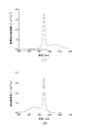
- FIG. 2 is a schematic view showing a stimulated emission cross section and an absorption cross section of Yb-added silica glass fiber.
- FIG. 2 (1) shows a stimulated emission cross section
- FIG. 2 (2) shows an absorption cross section.
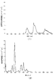
- FIG. 3 is a schematic view showing a stimulated emission cross section and an absorption cross section of Nd-added silica glass fiber.
- FIG. 3 (1) shows a stimulated emission cross section
- FIG. 3 (2) shows an absorption cross section.
- 1064 nm is selected as the oscillation wavelength. That is, the seeder 1 including SESAM 13 is configured to oscillate at 1064 nm.
- the absorption of the Yb-added silica glass fiber is small at 1064 nm and is almost zero.
- the stimulated emission cross section of the Nd-added silica glass at 1064 nm greatly exceeds 1.0 ⁇ 10-20 cm 2.
- FIG. 3 (1) shows a stimulated emission cross section of the Nd-added silica glass at 1064 nm greatly exceeds 1.0 ⁇ 10-20 cm 2.
- FIG. 3 (1) shows a stimulated emission cross section of the Nd-added silica glass at 1064 nm greatly exceeds 1.0 ⁇ 10-20 cm 2.
- the induced release cross-sectional area of the Yb-added silica glass at 1064 nm is about 0.2 ⁇ 10-20 cm 2
- the Nd-added silica glass fiber is compared with the Yb-added silica glass fiber. It has a very large induced emission cross section at 1064 nm. That is, in the seed laser element 11, Nd is adopted with priority given to a large stimulated emission cross section.
- FIG. 4 is a diagram schematically showing laser excitation in the configuration of the embodiment.
- the seed laser element 11 which is an Nd-added silica glass fiber
- pumping is performed from the ground level E 0 by the seeder excitation laser light
- Nd is excited to the excitation level E 1 .
- Nd there is a level of E 2 lower than E 1 level
- the Nd excited to E 1 fell in E 2 by a non-radiative transition
- further incident light 1064nm from the level E 2 fall in E 3 close to the ground level E 0.
- light of 1064 nm is stimulated and emitted.
- Nd drops from E 3 to E 0 due to the non-radiative transition.
- the excitation light that excites the ground level E 0 to E 1 has a wavelength of 804 nm.
- the Yb-doped silica glass fiber a is amplifying element 21, there is an energy level E 2 'for emitting light of 1064nm wavelength.
- E 2 energy level
- Yb fell 'E 2 by non-radiative transitions after being excited' E 1, to stimulated emission light of 1064nm when falling to the ground level E 0 'therefrom.
- the 'E 1 from' ground level E 0, is excited by the excitation laser light.
- the difference Delta] E of the energy level from E 0 to E 1 'Comparing the, case of a combination of Nd and Yb, ⁇ E> ⁇ E' difference Delta] E of the 'E 1 from' E 0 and It is a point that has become. That is, the pumping amount in the case of laser amplification can be made smaller than the pumping amount in the case of laser oscillation.
- a semiconductor laser having a wavelength of 975 nm is used as the amplification excitation laser source 22, and a laser diode having a wavelength longer than that of the seeder excitation laser source 3 is used.
- the longer the wavelength of the laser source the easier it is to oscillate, the more stable it is, and the cheaper it is. Therefore, it is significant that the configuration of the embodiment using the excitation laser having a long wavelength due to the small pumping amount can achieve stable performance at low cost.
- the amplifier 2 it is necessary to lengthen the optical path length of the amplification element 21 in order to increase the amplification factor, and therefore, the amplification excitation laser source 22 also has a high output. In this sense as well, the one with a long wavelength is preferable.
- the seeder 1 it is prioritized to oscillate the laser, and as long as the oscillation threshold is exceeded, the output of the pumped laser source 3 for the seeder does not need to be so large. Therefore, there is no problem even if a laser source having a large pumping amount and a short wavelength is used.
- the configuration of the above embodiment is an optimized configuration in consideration of these circumstances. As can be seen from FIG. 4, the above point can be regarded as a difference with respect to the oscillation wavelength, and the wavelength of the amplification excitation laser source 22 is expressed as having a smaller difference with respect to the oscillation wavelength than the seeder excitation laser source 3. You can also.
- the pulsed laser light source device of the embodiment also has a great feature in the method of manufacturing the laser element 11 for seeds, which is an Nd-added silica glass fiber. This point will be described below.
- FIG. 5 is a schematic view showing a method of manufacturing the seed laser element 11 included in the pulsed laser light source device of the embodiment.
- the seed laser element 11 is a fiber composed of a core 111 and a clad 112, and the seeder 1 is a kind of fiber laser oscillator.
- the seed laser element 11 is suitably manufactured by drawing using a base material obtained by the zeolite method. Specifically, as shown in FIG. 5, the Nd ion-exchanged zeolite powder 61 and the silica glass powder 62 are uniformly mixed, placed in a container, heated, pressurized and fired to obtain a fired body. The fired body is further heated in vacuum to obtain a glass molded body, and an Nd-added glass molded body 63 is obtained.
- the Nd-added glass molded body 63 is cut out and ground to obtain a cylindrical (or linear cross-section) core base material 64 having a diameter of about 1 to 10 mm.
- the core base material 64 is inserted into a silica tube (clad base material) 65 having a circular cross section to form a fiber base material, which is heated and drawn into a fiber shape.
- a silica tube (clad base material) 65 having a circular cross section to form a fiber base material, which is heated and drawn into a fiber shape.
- the seed laser element 11 according to the embodiment can be obtained.
- the cross-sectional shape of the core base material 64 does not have to be circular, and the clad base material 65 may be an annular shape other than a circular tube.
- the Nd-added glass molded body 63 obtained by the zeolite method is used as the core base material 64, but the manufacturing of the Nd-added glass molded body by the zeolite method is described in Patent Document 1 and Patent Document 2. Since it is disclosed in, it can be referred to.
- a method of heating a silica glass wire and immersing it in a solution containing Nd to infiltrate Nd from the outer surface into the inside is adopted.
- Nd-added silica glass fiber having good optical properties can be easily obtained.
- a thinning unit 5 is provided between the seeder 1 and the amplifier 2.
- the thinning unit 5 is a mechanism for adjusting the irradiation energy by periodically thinning the pulse from the pulse train of the short pulse and high-repetition laser light oscillated from the seeder 1.
- the thinning unit 5 has a mechanism using an AO modulator (acousto-optic modulator) 51.
- the AO modulator 51 is provided with an RF driver 52.
- the RF driver 52 is a driver that intermittently inputs an RF signal to the AO modulator 51 to operate it.
- the RF signal is on, the pulsed light is diffracted and the primary diffracted light travels in the optical path.
- the RF signal is off, only the 0th order light is emitted, and the pulsed light is out of the optical path. Therefore, the pulse train is thinned out by turning the RF signal on and off.
- the incident side lens 53 and the emitting side lens 54 are arranged.
- the light from the seeder coupling fiber 42 becomes a parallel beam (or is focused) by the incident side lens 53, passes through the AO modulator 51, and then is focused by the exit side lens 54 to the amplification element 21. It is configured to be incident.
- the seeder excitation laser source 3 operates, and the seeder excitation laser light is introduced into the seed laser element 11 via the seeder coupler 4.
- Nd in the seed laser element 11 is excited, a population inversion occurs, and light in the 1064 nm band is induced and emitted.
- Light having a slightly different wavelength in the longitudinal mode has a particularly high intensity due to interference at the portion where the positions of the peaks are aligned, resonates between the SESAM 13 and the output mirror 12, and oscillates by the Q-switch mode lock.
- Laser oscillation is pulse oscillation with a repeating period according to the resonator length.
- the pulse train oscillated from the seeder 1 is shown as P1 in FIG.
- the pulse train P1 of the oscillated laser light is thinned out by the thinning unit 5 as shown in the lower part of FIG. 1 to become P2.
- the output waveform (ultrasonic output control waveform) of the RF driver 52 that performs digital modulation at this time is shown as D.
- the pulse train P2 reaches the amplifier 2 and is amplified to become the pulse train P3, which is emitted from the amplification coupling fiber 23.
- Nd is used as the laser medium in the seed laser element 11
- Yb is used as the amplification medium in the amplification element 21, so that the function as a light source is used.
- It is a light source device that is comparable in terms of overall efficiency while improving its performance. That is, the seed laser element 11 emits sufficient seed laser light even with a short length due to the large stimulated emission cross section, and the amplification element 22 amplifies the seed laser light with high quantum efficiency and a small absorption cross section. There is. Therefore, it is possible to emit pulsed laser light having a high repetition frequency, and the efficiency at that time can be sufficiently sufficient.
- the fact that the seed laser element 11 and the amplification element 21 are fibers means that in addition to being able to efficiently obtain high-quality pulsed laser light, it is easy to irradiate an object in a state of being focused on a minute spot. There is an advantage. That is, since the seed laser light and each excitation laser light are introduced into a narrow space called the core and stimulated and stimulated emission are performed in a confined state, high-quality pulsed laser light is efficiently output.
- the host material is silica glass in this embodiment, it is inexpensive and has stable performance, and high-quality pulsed laser light can be stably obtained regardless of the environment such as temperature and humidity.
- the host material does not have to be silica glass, and other host materials such as YAG and fluoride glass can be appropriately selected and used.
- the fact that the seed laser element 11 is a single mode fiber has an advantage that spatial mode control such as mode lock becomes easy.
- the pulse oscillation is performed by using the Q-switch mode lock in the resonator 10 including the SESAM 13, energy efficiency can be increased even when outputting a pulse train having a high repetition frequency. ing. This point will be described below.
- the pulsed laser light source device is used for ablation not only in the medical field but also in the industrial field such as laser processing.
- Non-Patent Document 1 in the case of laser irradiation for dental treatment, a pulse of 4 ⁇ J per pulse is 1.7 GHz as compared with a case of irradiating a pulse of 100 ⁇ J per pulse at a repetition frequency of 1 kHz. It has been reported that irradiation without a set repetition frequency of 1 kHz can be performed without carbonization or cracks by irradiating an irradiation set with a repetition frequency at a set repetition frequency of 1 kHz.
- Non-Patent Document 2 discloses a technique for increasing the repetition frequency using division and delay.
- the 108 MHz laser light is divided into two (demultiplexed), one laser light is delayed with respect to the other laser light by a pulse period of 1/2 minute, and then the two are combined, and this is 5 By repeating this time, the frequency is increased to 3.46 GHz.
- Non-Patent Document 2 since the peak intensity of the pulse is halved each time the demultiplexing is performed, the peak of each pulse having a high repetition frequency is reduced to 1/32 of the original. Further, since a loss occurs each time the demultiplexing and the combined wave occur, the peak intensity is further lowered, and a large loss that cannot be ignored as a whole occurs. For example, if there is a loss of 3 dB for each demultiplexing wave, and if there is originally 100 ⁇ J of energy per pulse, the total loss is 18 dB, which is reduced to 0.25 ⁇ J.
- the Q-switch mode lock in the seeder 1 including SESAM 13 since the Q-switch mode lock in the seeder 1 including SESAM 13 is used, there is no loss as in the case of repeating demultiplexing and merging, and processing due to intensity fluctuation between pulses is not performed. There is no problem such as deterioration of accuracy.
- the stimulated emission In the state where the absorption by the saturable absorber 132 in SESAM 13 is not saturated, the stimulated emission has not started, but during this period, the laser medium (rare earth material) is excited to the laser level one after another to generate energy. There is no loss because it is accumulated and stimulated emission occurs at once when the absorption reaches saturation (the stage where the overlapping part of the mountain in the longitudinal mode passes) and the energy is discharged.
- the resonator length in the seeder 1 may be made variable so that the repeat frequency can be adjusted.
- one pulse of laser oscillation occurs when the peak and the overlapping portion of the vertical mode pass through the seed laser element 11 once. Therefore, if the resonator length is changed, the interval in one passage is changed. The length of is changed. That is, the repetition frequency of the pulse is changed.
- a precision position adjustment such as a mechanism using a piezo element is provided on either the SESAM 13 or the output mirror 12 so that the position can be changed.
- the SESAM 13 and / or the output mirror 12 may be in contact with the seed laser element 11, but are usually arranged in a separated state.
- Nd is used as the laser medium in the seed laser element 11, and Yb is used as the amplification medium in the amplification element 21, but these are examples of rare earth materials.
- rare earth materials that can be adopted in the present invention.
- thulium (Tm) and erbium (Er) can have a larger stimulated emission cross section than holmium (Ho). Therefore, a combination in which Tm-added silica glass is used for the seed laser element 11 and Ho-added silica glass is used for the amplification element 21, and Er-added silica glass is used for the seed laser element 11, and the amplification element 21 is used.
- Ho-added silica glass There may be a combination that employs Ho-added silica glass.
- the energy (level difference) when the seeder excitation laser source 3 excites the seed laser element 11 to the laser level is amplified.
- the energy required by the excitation laser source 22 for exciting the amplification element 21 to the laser level is smaller.
- the pulsed laser light source device of the embodiment can be used for various processing involving ablation.
- the thinning unit 5 using the AO modulator 51 is adopted, but it can be appropriately changed to another configuration such as one adopting a mechanical mechanism such as a shutter.
- thinning out the pulse train is not essential in the present invention, and the object may be irradiated without thinning out.
- the coupling element in addition to WDM, various couplers such as a planar waveguide can be used, and a spatial coupling element such as a half mirror may be used.
- a fiber for the optical path from the seeder 1 to the amplifier 2 and if necessary, a lens or a mirror may be arranged to guide the light in space.
- SESAM 13 was used in Cedar 1, it is not essential, and it is possible that Cedar 1 is configured by using other reflective optical elements. That is, another SAM using a saturable absorber other than the semiconductor may be used, or another reflecting element such as an FBG (Fiber Bragg Grating) may be used to configure the seeder 1.
- FBG Fiber Bragg Grating
- a configuration for realizing the Q-switch mode lock in addition to the case of using the SAM, a configuration of performing the active mode lock using an electro-optical modulator such as a Pockels cell, an AO modulator, or the like may be adopted. ..
- an electro-optical modulator such as a Pockels cell, an AO modulator, or the like
- the seed laser element 11 and the seeder coupling fiber 42 may be fused via the output mirror 12 without using the lens group 41.
- the thinning unit 5 and when a fiber coupling type AO modulator is used, the lenses 53 and 54 may not be used because the fibers are fused to each other.
- a silica glass molded body in which 1.2% by weight of Nd was added was produced by a zeolite method, and a columnar shape having a diameter of 3 mm was formed by cutting and grinding. This was inserted into a silica glass circular tube and used as a base material, and was drawn with a drawing device so as to have an outer diameter (diameter) of 125 ⁇ m to obtain Nd-added silica glass fiber.
- This fiber was cut to a length of 60 mm, both ends were polished, and then coated with an antireflection film or the like to obtain a seed laser element 11.
- the seed laser element 11 was placed in a resonator 10 using SESAM 13 manufactured so as to resonate at 1064 nm.
- SESAM 13 As the amplifier 2, a Yb-added silica glass fiber manufactured by Nufern of the United States (East Granby, Connecticut, 7 Airport Park Road East Granby, CT) is used with a length of 3 m, and the excitation laser source 22 for amplification is used.
- a semiconductor laser having a wavelength of 975 nm was used.
- the pulsed laser light source device configured in this way was operated and its output was measured with an optical spectrum analyzer, it was confirmed that the pulse laser light source device oscillated at a wavelength of 1064 nm. Moreover, when the frequency was repeatedly confirmed with an RF spectrum analyzer, it was 2.7 GHz. When the output was measured with a laser power meter, it was 0.15 mW at the time of the output of the seeder 1, and 22.3 mW as the output of the amplifier 2. Therefore, it was confirmed that the amplification factor by the amplifier 2 was 150.
Landscapes
- Physics & Mathematics (AREA)
- Engineering & Computer Science (AREA)
- Electromagnetism (AREA)
- Optics & Photonics (AREA)
- Plasma & Fusion (AREA)
- Life Sciences & Earth Sciences (AREA)
- Health & Medical Sciences (AREA)
- Chemical & Material Sciences (AREA)
- Surgery (AREA)
- Otolaryngology (AREA)
- General Life Sciences & Earth Sciences (AREA)
- Heart & Thoracic Surgery (AREA)
- Medical Informatics (AREA)
- Molecular Biology (AREA)
- Animal Behavior & Ethology (AREA)
- General Health & Medical Sciences (AREA)
- Public Health (AREA)
- Veterinary Medicine (AREA)
- Biomedical Technology (AREA)
- Geochemistry & Mineralogy (AREA)
- Manufacturing & Machinery (AREA)
- Nuclear Medicine, Radiotherapy & Molecular Imaging (AREA)
- Materials Engineering (AREA)
- Organic Chemistry (AREA)
- Mechanical Engineering (AREA)
- Lasers (AREA)
- Laser Surgery Devices (AREA)
- Laser Beam Processing (AREA)
- Manufacture, Treatment Of Glass Fibers (AREA)
Abstract
増幅器によって高出力としつつも全体のエネルギー効率が改善されたパルスレーザー光源装置を提供する。 シーダー1に設けられたシード用レーザー素子11はシーダー用励起レーザー源3からの波長804nmの光により励起され、出力ミラー12とSESAM13で構成された共振器10で共振して波長1064nmで発振する。発振したシードレーザー光は、増幅用励起レーザー源22からの波長975nmの光で励起されている増幅素子21に入射して誘導放出により増幅される。シード用レーザー素子11はネオジム添加のシリカガラスファイバーであり、増幅素子21はイッテルビウム添加のシリカガラスファイバーである。
Description
この出願の発明は、パルスレーザー光を出射するパルスレーザー光源装置に関するものである。
パルスレーザー光を出射するパルスレーザー光源装置は、種々の用途で使用されている。例えば、レーザー切断やレーザー孔開けといった各種加工用に、パルスレーザー光源装置が使用されている。パルスレーザーの場合、パルスの繰り返し周波数を調整することで適宜のエネルギーを与えることができ、対象物の損傷を避けつつ所望の加工を行うことが容易だからである。
このようなパルスレーザーの代表的なものは、希土類材料や遷移金属をレーザー媒質として添加した固体レーザーである。レーザー媒質は、透光性の材料(以下、ホスト材料という。)に添加される。レーザー媒質が添加されたホスト材料はファイバー状やロッド状に形成されてレーザー素子とされ、共振器が設けられてレーザー発振器が構成される。通常、レーザー素子は、励起レーザー源からのレーザービームにより励起されてレーザー発振する。
このような固体発光のパルスレーザーでは、出力エネルギーを高めるため、レーザー増幅の構成が採用されることが多い。レーザー増幅を行う場合、レーザー発振におけるレーザー媒質と同じ材料の増幅素子が使用される。増幅素子に別の励起レーザー源からのレーザービームを導入して励起しておき、レーザー共振器から出力されたレーザービームを入射させ、誘導放出により増幅する。
"Ablation-cooled material removal with ultrafast bursts of pulses", Can Kerse et al, Nature, Vol. 537, p84-89
"3.5-GHz intra-burst repetition rate ultrafast Yb-doped fiber laser", Can Kerse et al, Optics Communications 366(2016), p404-409
上述した固体発光レーザーにおいて、レーザー媒質としては、ネオジム(Nd)やイッテルビウム(Yb)がしばしば使用される。このうち、NdはYbに比べて大きな誘導放出断面積を持っているものの、幾つかの欠点がある。一つは、高濃度化した場合の問題である。エネルギー効率を高くして出力を大きくするため、NdやYbの添加量を多くすることが行われるが、Ndの場合、濃度消光と呼ばれる現象が顕著となる。Ndの添加量を多くすると、均一に散在させることが難しいことから、Nd原子同士が接近して濃度消光が生じ易い。
もう一つは、量子欠損の問題である。誘導放出準位の励起の際の量子効率は、Ybの場合は90%以上であるものの、Ndは量子欠損が大きいため、76.1%程度である。このため、NdはYbに比べてエネルギー効率が悪い。このような事情から、レーザー媒質としてはYbが選ばれることが多く、Yb添加のシーダーから出力されるレーザービームをYb添加の増幅媒体を励起して増幅する構成が採用されることが多い。
しかしながら、その反面、Ybの場合、増幅器のところで吸収が大きく、大きな損失が生じる。このため、吸収が少ない波長に発振波長をずらす工夫がされるが、この結果、シーダーにおいて誘導放出断面積が相対的に小さい波長で発振させることになり、光源としての機能性を高めることができない。
本願発明は、増幅器を備えたパルスレーザー光源装置のこのような技術課題を考慮して為されたものであり、光源としての機能性を高くしつつも全体のエネルギー効率が十分に確保されたパルスレーザー光源装置を提供することを目的としている。
本願発明は、増幅器を備えたパルスレーザー光源装置のこのような技術課題を考慮して為されたものであり、光源としての機能性を高くしつつも全体のエネルギー効率が十分に確保されたパルスレーザー光源装置を提供することを目的としている。
上記課題を解決するため、本願発明のパルスレーザー光源装置は、シードレーザー光を出力するシーダーと、シーダーから出力されたシードレーザー光を増幅する増幅器とを備えている。
このパルスレーザー光源装置において、シーダーは、第一の希土類材料が添加されたホスト材料より成るシード用レーザー素子を含んでおり、増幅器は、第二の希土類材料が添加されたホスト材料より成る増幅素子を含んでいる。
また、シーダーから出力されるシードレーザー光の発振波長において、第一の希土類材料は第二の希土類材料よりも誘導放出断面積が大きい材料である。
上記課題を解決するため、本願発明のパルスレーザー光源装置は、シードレーザー光を出力するシーダーと、シーダーから出力されたシードレーザー光を増幅する増幅器とを備えている。
このパルスレーザー光源装置において、シーダーは、第一の希土類材料が添加されたホスト材料より成るシード用レーザー素子と、発振波長の光を誘導放出する準位にシード用レーザー素子を励起するシーダー用励起レーザー源とを含んでおり、増幅器は、第二の希土類材料が添加されたホスト材料より成る増幅素子と、発振波長の光を誘導放出する準位に増幅素子を励起する増幅用励起レーザー源とを含んでおり、増幅用励起レーザー源の波長は、シーダー用励起レーザー源の波長より長い。
上記課題を解決するため、本願発明のパルスレーザー光源装置は、発振波長の光を誘導放出する際の第二の希土類材料の量子効率が、第一の希土類材料に比べて大きいという構成を持ち得る。
上記課題を解決するため、本願発明のパルスレーザー光源装置は、第一の希土類材料がネオジムであって第二の希土類材料がイッテルビウムであるか、第一の希土類材料がツリウムであって第二の希土類材料はホルミウムであるか、又は第一の希土類材料がエルビウムであって第二の希土類材料はホルミウムであるという構成を持ち得る。
上記課題を解決するため、本願発明のパルスレーザー光源装置は、シード用レーザー素子が、第一の希土類材料が添加されたホスト材料をコアとしたファイバーであり、増幅素子が、第二の希土類材料が添加されたホスト材料をコアとしたファイバーであるという構成を持ち得る。
上記課題を解決するため、本願発明のパルスレーザー光源装置は、シーダーが、シード用レーザー素子を内蔵した共振器を含んでおり、共振器を構成する一方のミラーは可飽和ミラーであって、共振器は発振波長においてQスイッチモードロックを達成するものであるという構成を持ち得る。
上記課題を解決するため、本願発明のパルスレーザー光源装置は、シーダーから出力されるパルスの繰り返し周波数は1GHz以上であるという構成を持ち得る。
上記課題を解決するため、本願発明のパルスレーザー光源装置は、シーダーと増幅器との間の光路上に、パルス列からパルスを間引く間引きユニットが設けられているという構成を持ち得る。
上記課題を解決するため、本願発明のパルスレーザー光源装置は、アブレーション用であり得る。
上記課題を解決するため、本願発明のパルスレーザー光源装置において、ホスト材料はシリカガラスであり得る。
上記課題を解決するため、本願発明の希土類添加ファイバー製造方法は、光の誘導放出素子としての希土類添加ファイバーを製造する方法であって、
希土類材料が固定されたゼオライト粉末とホスト材料粉末とを混合して焼成することで希土類添加成形体を得るステップと、
希土類添加成形体から切り出して研磨することで円柱状のコア母材を得るステップと、 コア母材を円管状のクラッド母材に挿入してファイバー母材を得るステップと、
ファイバー母材を加熱しながら線引きして希土類添加ファイバーを得るステップと
を有する。
上記課題を解決するため、本願発明の希土類添加ファイバー製造方法において、ホスト材料はシリカガラスであり得る。
このパルスレーザー光源装置において、シーダーは、第一の希土類材料が添加されたホスト材料より成るシード用レーザー素子を含んでおり、増幅器は、第二の希土類材料が添加されたホスト材料より成る増幅素子を含んでいる。
また、シーダーから出力されるシードレーザー光の発振波長において、第一の希土類材料は第二の希土類材料よりも誘導放出断面積が大きい材料である。
上記課題を解決するため、本願発明のパルスレーザー光源装置は、シードレーザー光を出力するシーダーと、シーダーから出力されたシードレーザー光を増幅する増幅器とを備えている。
このパルスレーザー光源装置において、シーダーは、第一の希土類材料が添加されたホスト材料より成るシード用レーザー素子と、発振波長の光を誘導放出する準位にシード用レーザー素子を励起するシーダー用励起レーザー源とを含んでおり、増幅器は、第二の希土類材料が添加されたホスト材料より成る増幅素子と、発振波長の光を誘導放出する準位に増幅素子を励起する増幅用励起レーザー源とを含んでおり、増幅用励起レーザー源の波長は、シーダー用励起レーザー源の波長より長い。
上記課題を解決するため、本願発明のパルスレーザー光源装置は、発振波長の光を誘導放出する際の第二の希土類材料の量子効率が、第一の希土類材料に比べて大きいという構成を持ち得る。
上記課題を解決するため、本願発明のパルスレーザー光源装置は、第一の希土類材料がネオジムであって第二の希土類材料がイッテルビウムであるか、第一の希土類材料がツリウムであって第二の希土類材料はホルミウムであるか、又は第一の希土類材料がエルビウムであって第二の希土類材料はホルミウムであるという構成を持ち得る。
上記課題を解決するため、本願発明のパルスレーザー光源装置は、シード用レーザー素子が、第一の希土類材料が添加されたホスト材料をコアとしたファイバーであり、増幅素子が、第二の希土類材料が添加されたホスト材料をコアとしたファイバーであるという構成を持ち得る。
上記課題を解決するため、本願発明のパルスレーザー光源装置は、シーダーが、シード用レーザー素子を内蔵した共振器を含んでおり、共振器を構成する一方のミラーは可飽和ミラーであって、共振器は発振波長においてQスイッチモードロックを達成するものであるという構成を持ち得る。
上記課題を解決するため、本願発明のパルスレーザー光源装置は、シーダーから出力されるパルスの繰り返し周波数は1GHz以上であるという構成を持ち得る。
上記課題を解決するため、本願発明のパルスレーザー光源装置は、シーダーと増幅器との間の光路上に、パルス列からパルスを間引く間引きユニットが設けられているという構成を持ち得る。
上記課題を解決するため、本願発明のパルスレーザー光源装置は、アブレーション用であり得る。
上記課題を解決するため、本願発明のパルスレーザー光源装置において、ホスト材料はシリカガラスであり得る。
上記課題を解決するため、本願発明の希土類添加ファイバー製造方法は、光の誘導放出素子としての希土類添加ファイバーを製造する方法であって、
希土類材料が固定されたゼオライト粉末とホスト材料粉末とを混合して焼成することで希土類添加成形体を得るステップと、
希土類添加成形体から切り出して研磨することで円柱状のコア母材を得るステップと、 コア母材を円管状のクラッド母材に挿入してファイバー母材を得るステップと、
ファイバー母材を加熱しながら線引きして希土類添加ファイバーを得るステップと
を有する。
上記課題を解決するため、本願発明の希土類添加ファイバー製造方法において、ホスト材料はシリカガラスであり得る。
以下に説明する通り、本願発明のパルスレーザー光源装置によれば、シード用レーザー素子と増幅素子とにおいて異なる希土類材料を選定しており、シード用レーザー素子は増幅素子よりも大きな誘導放出断面積を有しているので、光源の機能が高められる。また、増幅素子について発振波長における吸収が少ない希土類材料を選定することができるので、光源全体としての効率低下を抑制することができる。
また、本願発明のパルスレーザー光源装置によれば、増幅用励起レーザー源の波長は、シーダー用励起レーザー源の波長より長いので、安定した性能を安価に達成できる。
また、シード用レーザー素子における希土類材料に比べて量子効率が大きい希土類材料を増幅素子について採用すると、増幅の際の効率が高くなるので、上記効果がより高くなる。
また、シード用レーザー素子が、第一の希土類材料が添加されたホスト材料をコアとしたファイバーであり、増幅素子が、第二の希土類材料が添加されたホスト材料をコアとしたファイバーである構成では、環境によらず品質の良いパルスレーザー光を安定して照射することができ、且つ微小スポットの集光した状態で対象物に照射するのが容易となる。
また、シーダーが、シード用レーザー素子を内蔵した共振器を含んでおり、共振器を構成する一方のミラーは可飽和ミラーであって、共振器は発振波長においてQスイッチモードロックを達成するものである構成では、分波と合波を繰り返す際のような損失はなく、パルス間の強度変動による加工精度低下等の問題もない状態で高繰り返し周波数のパルス列を出力することができる。
また、パルス列からパルスを間引く間引きユニットが設けられている構成では、対象物に対して最適なエネルギーとなるようにパルス列を照射することが容易であり、アブレーション用である場合に特に好適となる。
また、希土類材料が固定されたゼオライト粉末とホスト材料粉末とを混合、焼成することで得たコア母材により希土類添加ファイバーを得る製造方法によれば、良好な光学特性の希土類添加ファイバーを容易に得ることができる。
また、ホスト材料がシリカガラスである構成では、安価で且つ性能が安定し、温度や湿度等の環境によらず品質の良いパルスレーザー光が安定して得られる。
また、本願発明のパルスレーザー光源装置によれば、増幅用励起レーザー源の波長は、シーダー用励起レーザー源の波長より長いので、安定した性能を安価に達成できる。
また、シード用レーザー素子における希土類材料に比べて量子効率が大きい希土類材料を増幅素子について採用すると、増幅の際の効率が高くなるので、上記効果がより高くなる。
また、シード用レーザー素子が、第一の希土類材料が添加されたホスト材料をコアとしたファイバーであり、増幅素子が、第二の希土類材料が添加されたホスト材料をコアとしたファイバーである構成では、環境によらず品質の良いパルスレーザー光を安定して照射することができ、且つ微小スポットの集光した状態で対象物に照射するのが容易となる。
また、シーダーが、シード用レーザー素子を内蔵した共振器を含んでおり、共振器を構成する一方のミラーは可飽和ミラーであって、共振器は発振波長においてQスイッチモードロックを達成するものである構成では、分波と合波を繰り返す際のような損失はなく、パルス間の強度変動による加工精度低下等の問題もない状態で高繰り返し周波数のパルス列を出力することができる。
また、パルス列からパルスを間引く間引きユニットが設けられている構成では、対象物に対して最適なエネルギーとなるようにパルス列を照射することが容易であり、アブレーション用である場合に特に好適となる。
また、希土類材料が固定されたゼオライト粉末とホスト材料粉末とを混合、焼成することで得たコア母材により希土類添加ファイバーを得る製造方法によれば、良好な光学特性の希土類添加ファイバーを容易に得ることができる。
また、ホスト材料がシリカガラスである構成では、安価で且つ性能が安定し、温度や湿度等の環境によらず品質の良いパルスレーザー光が安定して得られる。
以下、この出願の発明を実施するための形態(実施形態)について説明する。
図1は、実施形態に係るパルスレーザー光源装置の概略図である。実施形態のパルスレーザー光源装置は、シードレーザー光を出力するシーダー1と、シーダー1から出力されたシードレーザー光を増幅する増幅器2とを備えている。シーダー1は、誘導放出が行われる際の準位(レーザー準位)に励起されるシード用レーザー素子11を含んでいる。
図1は、実施形態に係るパルスレーザー光源装置の概略図である。実施形態のパルスレーザー光源装置は、シードレーザー光を出力するシーダー1と、シーダー1から出力されたシードレーザー光を増幅する増幅器2とを備えている。シーダー1は、誘導放出が行われる際の準位(レーザー準位)に励起されるシード用レーザー素子11を含んでいる。
この実施形態では、シード用レーザー素子11は、レーザー光で励起される構成が採用されており、シーダー用励起レーザー源3が設けられている。シーダー用励起レーザー源3としては、連続発振の半導体レーザーが使用されている。
図1に示すように、シーダー1に対してはレンズ群41を介してシーダー用カップリングファイバー42が設けられている。シーダー用カップリングファイバー42にはWDM(Wavelength Division Multiplexing)カプラのようなシーダー用結合素子4が設けられており、シーダー用励起レーザー源3からのレーザー光はシーダー用結合素子4及び出力ミラー12を通してシーダー1内のシード用レーザー素子11に入射し、シード用レーザー素子11を励起するよう構成されている。
図1に示すように、シーダー1に対してはレンズ群41を介してシーダー用カップリングファイバー42が設けられている。シーダー用カップリングファイバー42にはWDM(Wavelength Division Multiplexing)カプラのようなシーダー用結合素子4が設けられており、シーダー用励起レーザー源3からのレーザー光はシーダー用結合素子4及び出力ミラー12を通してシーダー1内のシード用レーザー素子11に入射し、シード用レーザー素子11を励起するよう構成されている。
シード用レーザー素子11は、図1中に拡大して示すように、コア111とクラッド112から成るファイバー状であり、保護及び補強用のフェルール113で覆われた構造となっている。長さは10~100mm程度であるので、短いファイバー状部材ということができる。シード用レーザー素子11のコア111は、レーザー媒体として希土類材料を含んでおり、実質的なレーザー素子である。この実施形態では、シード用レーザー素子11における希土類材料はネオジム(Nd)であり、ホスト材料にはシリカガラスが選定されている。即ち、コア111はNd添加シリカガラスとなっている。また、クラッド112はNd添加無しのシリカガラスである。シード用レーザー素子11におけるコア111の直径は1~20μm程度、クラッド112を含む全体の直径は80~1000μm程度である。ファイバーであるシード用レーザー素子11の伝搬モードは、シングルモード(シングルモードファイバー)である。
このようなシード用レーザー素子11を内蔵するシーダー1は、共振器10を含んでおいる。共振器10は、共振とパルス発振との両方を達成するものとなっており、この実施形態では、Qスイッチモードロックを行うものとなっている。より具体的に説明すると、シーダー1の共振器10において、可飽和ミラー(SAM)が使用されている。この実施形態では、SAMの中でも、特に半導体可飽和ミラー(SESAM)13が使用されている。
SESAM13は、共振器10を構成する一方のミラーである。共振器10を構成する他方のミラーは、出力ミラー12である。出力ミラー12は、例えば30~99%反射のミラーであり、残りを透過させて出力するミラーである。
SESAM13は、共振器10を構成する一方のミラーである。共振器10を構成する他方のミラーは、出力ミラー12である。出力ミラー12は、例えば30~99%反射のミラーであり、残りを透過させて出力するミラーである。
図1中に拡大して示すように、SESAM13は、DBR(Distributed Bragg Reflector,分布ブラッグ反射鏡)131の入射側に可飽和吸収体132を積層した構造のミラーであり、SESAM13は、可飽和吸収体132がInGaAsのような半導体で形成されている。SESAM13において、可飽和吸収体132は量子井戸構造を有しており、光がある強度になると吸収が飽和し、それ以上の光は透過してDBR131に達する。
DBR131は、1/4波長の厚みを持ち且つ屈折率の異なる層が積層された構造(例えばGaAs/AlAs)を有し、ブラッグ反射と光の干渉を利用して特定の波長の光のみを特に強く反射する。
DBR131は、1/4波長の厚みを持ち且つ屈折率の異なる層が積層された構造(例えばGaAs/AlAs)を有し、ブラッグ反射と光の干渉を利用して特定の波長の光のみを特に強く反射する。
シーダー用励起レーザー源3からのレーザー光(CW)がシード用レーザー素子11に導入されると、シード用レーザー素子11中の希土類材料(レーザー媒質)が励起され、反転分布が生じて光が誘導放出される。この際、周知のように、共振器10内では複数の縦モードの定在波が生じ得るが、位相が揃っていない状態でSESAM13に達すると、干渉により光が弱いために可飽和吸収体132で吸収される。位相が揃った状態では干渉により強くなっているため、吸収の飽和により可飽和吸収体132を透過してDBR131に達して反射する。即ち、位相が揃ったところで特に強い共振が生じ、誘導放出が一気に生じてQスイッチモードロックでのレーザー発振が達成される。尚、DBR131は、設定された発振波長の光を選択的に反射するよう設計、製作される。
一方、増幅器2は、図1に示すように、増幅素子21と、増幅用励起レーザー源22と、増幅用カップリングファイバー23等を備えている。増幅用カップリングファイバー23には、WDMカプラのような増幅用結合素子24が設けられている、増幅用励起レーザー源22からのレーザー光は増幅用結合素子24を経由して増幅素子21に導入し、増幅素子21を励起するよう構成されている。
増幅素子21は、増幅用励起レーザー源22からの増幅用励起レーザー光により励起されて誘導放出を行うことで、シーダー1から出力されたシードレーザー光を増幅する素子である。この実施形態では、増幅素子21は、シード用レーザー素子11と同様に希土類材料が添加された透光性材料で形成されている。
より具体的には、増幅素子21は、イッテルビウム(Yb)が添加されたシリカガラスで形成されている。形状はファイバー状である。即ち、Yb添加シリカガラスファイバーが増幅素子21として使用されている。
より具体的には、増幅素子21は、イッテルビウム(Yb)が添加されたシリカガラスで形成されている。形状はファイバー状である。即ち、Yb添加シリカガラスファイバーが増幅素子21として使用されている。
実施形態のようにシーダーの後段に増幅器を設ける場合、通常は、同様の誘導放出過程を利用するので、シーダー内のレーザー素子と同様の材料で形成された素子を増幅素子として用いる。しかしながら、この実施形態では、従来の常識に反し、敢えて異なる材料で形成された素子を増幅素子21として用いており、上記のようにYb添加シリカガラスファイバーとなっている。
このようにシード用レーザー素子11における希土類材料とは異なる希土類材料を添加した素子を増幅素子21として用いることは、光源としての機能性向上を意図した発明者による鋭意研究の結果である。以下、この点について説明する。
前述したように、希土類材料添加のレーザー素子においては、NdやYbが使用されるが、濃度消光や量子欠損の問題から、Ybが採用されることが多い。図2は、Yb添加のシリカガラスファイバーの誘導放出断面積と吸収断面積とを示した概略図である。図2(1)は誘導放出断面積、図2(2)は吸収断面積を示す。
前述したように、希土類材料添加のレーザー素子においては、NdやYbが使用されるが、濃度消光や量子欠損の問題から、Ybが採用されることが多い。図2は、Yb添加のシリカガラスファイバーの誘導放出断面積と吸収断面積とを示した概略図である。図2(1)は誘導放出断面積、図2(2)は吸収断面積を示す。
図2(1)に示すように、Ybの場合、1030nm付近で誘導放出断面積がピークを持つので、1030nmが発振波長とされる場合が多い。この場合、シード用レーザー素子11と増幅素子21とで同じ希土類材料を使用する構成では、増幅素子21でもYb添加のシリカガラスが使用されるが、図2(2)に示すように、Yb添加シリカガラスは1030nmにおいてもある程度の吸収が生じる。この吸収のために損失が生じ、この分でエネルギー効率が低下する。その上、吸収による発熱を抑えるために冷却手段が必要になり、さらにエネルギーが必要になって効率が低下する。
これらの問題を避けるため、吸収がほぼゼロになる1080nmに発振波長をずらし、1080nmで発振するようにシーダーを設計、製作することが考えられる。しかしながら、この構成では、誘導放出断面積が小さいところでレーザー発振をさせようとすることになるので、レーザー発振閾値が高くなり、シーダーとしての本来の機能が低下する。
このため、発明者らは、常識に反してシード用レーザー素子11の材料と増幅素子21の材料とを敢えて異なる材料とすることを想到するに至った。この実施形態では、シード用レーザー素子11については誘導放出断面積を優先させてNdを使用し、増幅素子21については量子効率の点で優れたYbを使用している。
このため、発明者らは、常識に反してシード用レーザー素子11の材料と増幅素子21の材料とを敢えて異なる材料とすることを想到するに至った。この実施形態では、シード用レーザー素子11については誘導放出断面積を優先させてNdを使用し、増幅素子21については量子効率の点で優れたYbを使用している。
図3は、Nd添加シリカガラスファイバーの誘導放出断面積と吸収断面積とを示した概略図である。同様に、図3(1)が誘導放出断面積、図3(2)が吸収断面積を示す。
この実施形態では、1064nmを発振波長として選定している。即ち、SESAM13を含むシーダー1は1064nmで発振するよう構成されている。図2(2)に示すように、Yb添加シリカガラスファイバーの吸収は1064nmにおいて小さく、ほぼゼロである。そして、図3(1)に示すように、1064nmにおけるNd添加シリカガラスの誘導放出断面積は1.0×10⁻²⁰cm2を大きく上回っている。一方、図2(1)に示すように、1064nmにおけるYb添加シリカガラスの誘導放出断面積は0.2×10⁻²⁰cm2程度であり、Nd添加シリカガラスファイバーはYb添加シリカガラスファイバーに比べて1064nmにおいて非常に大きな誘導放出断面積を有する。つまり、シード用レーザー素子11においては誘導放出断面積が大きいことを優先してNdを採用している。
この実施形態では、1064nmを発振波長として選定している。即ち、SESAM13を含むシーダー1は1064nmで発振するよう構成されている。図2(2)に示すように、Yb添加シリカガラスファイバーの吸収は1064nmにおいて小さく、ほぼゼロである。そして、図3(1)に示すように、1064nmにおけるNd添加シリカガラスの誘導放出断面積は1.0×10⁻²⁰cm2を大きく上回っている。一方、図2(1)に示すように、1064nmにおけるYb添加シリカガラスの誘導放出断面積は0.2×10⁻²⁰cm2程度であり、Nd添加シリカガラスファイバーはYb添加シリカガラスファイバーに比べて1064nmにおいて非常に大きな誘導放出断面積を有する。つまり、シード用レーザー素子11においては誘導放出断面積が大きいことを優先してNdを採用している。
レーザー発振、増幅の双方で励起レーザーを使用する構成では、ポンピングする量(エネルギー量)を小さくすることも重要である。実施形態の構成は、この点においても優位性を有する。この点について、図4を参照して説明する。図4は、実施形態の構成におけるレーザー励起について模式的に示した図である。
実施形態において、Nd添加シリカガラスファイバーであるシード用レーザー素子11では、基底準位E0からシーダー用励起レーザー光によりポンピングが行われ、Ndは励起準位E1に励起される。Ndは、E1より低い準位にE2という準位があり、E1に励起されたNdは、非輻射遷移によりE2に落ち、さらに1064nmの光が入射してこの準位E2から基底準位E0に近いE3に落ちる。この際、1064nmの光を誘導放出する。そして、Ndは、非輻射遷移によりE3からE0に落ちる。基底準位E0からE1への励起を行う励起光は、波長804nmである。
一方、Yb添加シリカガラスファイバーである増幅素子21には、1064nm波長の光を放出するエネルギー準位E2’が存在する。同様に、YbはE1’に励起された後に非輻射遷移によりE2’に落ち、そこから基底準位E0’に落ちる際に1064nmの光を誘導放出する。基底準位E0’からE1’には、励起レーザー光で励起される。
一方、Yb添加シリカガラスファイバーである増幅素子21には、1064nm波長の光を放出するエネルギー準位E2’が存在する。同様に、YbはE1’に励起された後に非輻射遷移によりE2’に落ち、そこから基底準位E0’に落ちる際に1064nmの光を誘導放出する。基底準位E0’からE1’には、励起レーザー光で励起される。
ここで重要なのは、E0からE1へのエネルギー準位の差ΔEと、E0’からE1’への差ΔE’とを比べると、NdとYbの組み合わせの場合、ΔE>ΔE’となっている点である。つまり、レーザー発振の際のポンピング量に比べレーザー増幅の場合のポンピング量が小さくできるということである。事実、この実施形態では、増幅用励起レーザー源22としては波長975nmの半導体レーザーを使用しており、シーダー用励起レーザー源3より波長が長いものを使用している。
一般的に、レーザー源は波長が長い方が発振が容易で安定しており、価格も安い。したがって、ポンピング量が小さいために長い波長の励起用レーザーを使用する実施形態の構成は、安定した性能を安価に達成できるという意義がある。また、増幅器2では、増幅率を上げるために増幅素子21の光路長を長くする必要があり、したがって増幅用励起レーザー源22も高出力のものが使用される。この意味でも、長波長のものの方が望ましい。
一方、シーダー1では、レーザー発振をさせることが優先であり、発振閾値を超えている限り、シーダー用励起レーザー源3の出力はそれほど大きくする必要はない。したがって、ポンピング量が大きくて短波長のレーザー源を使用しても、問題はない。上記実施形態の構成は、これらの事情を勘案して最適化された構成である。
尚、図4から解るように、上記の点は、発振波長に対する差として捉えると、増幅用励起レーザー源22の波長は、発振波長に対する差がシーダー用励起レーザー源3よりも小さいと表現することもできる。
尚、図4から解るように、上記の点は、発振波長に対する差として捉えると、増幅用励起レーザー源22の波長は、発振波長に対する差がシーダー用励起レーザー源3よりも小さいと表現することもできる。
実施形態のパルスレーザー光源装置は、Nd添加シリカガラスファイバーであるシード用レーザー素子11の製造方法においても大きな特徴点を有している。以下、この点を説明する。
図5は、実施形態のパルスレーザー光源装置が備えるシード用レーザー素子11の製造方法について示した概略図である。
図5は、実施形態のパルスレーザー光源装置が備えるシード用レーザー素子11の製造方法について示した概略図である。
この実施形態において、シード用レーザー素子11はコア111とクラッド112から成るファイバーであり、シーダー1は、ある種のファイバーレーザー発振器である。シード用レーザー素子11は、ゼオライト法により得られた母材を使用した線引きにより好適に製造される。
具体的に説明すると、図5に示すように、Ndイオン交換ゼオライト粉末61とシリカガラス粉末62とを均一に混合し、容器に入れて加熱、加圧して焼成し、焼成体を得る。
焼成体をさらに真空中で加熱してガラス成形体とし、Nd添加ガラス成形体63を得る。
具体的に説明すると、図5に示すように、Ndイオン交換ゼオライト粉末61とシリカガラス粉末62とを均一に混合し、容器に入れて加熱、加圧して焼成し、焼成体を得る。
焼成体をさらに真空中で加熱してガラス成形体とし、Nd添加ガラス成形体63を得る。
そして、Nd添加ガラス成形体63を切り出し、研削により直径が1~10mm程度の円柱状(ないしは断面円形の線状)のコア母材64とする。コア母材64を断面円形のシリカ管(クラッド母材)65に挿入してファイバー母材とし、加熱、線引きによりファイバー状とする。得られたファイバー66を所定の長さで切断することで、実施形態におけるシード用レーザー素子11が得られる。尚、コア母材64の断面形状は円形である必要はなく、クラッド母材65は円管以外の環状であっても良い。
上記の製造方法は、ゼオライト法により得られたNd添加ガラス成形体63をコア母材64とするものであるが、ゼオライト法によるNd添加ガラス成形体の製造については、特許文献1や特許文献2に開示されているので、参照することができる。
従来、Ndのような希土類材料を添加したシリカガラスファイバーを製造する場合、シリカガラス線材を加熱してNdを含む溶液中に浸し、外面からNdを内部に滲入させる方法が採用される。しかしながら、このような方法では、均一にNdを散在させることが難しく、良好な光学特性のものがえられない。実施形態の方法によれば、良好な光学特性のNd添加シリカガラスファイバーを容易に得ることができる。
従来、Ndのような希土類材料を添加したシリカガラスファイバーを製造する場合、シリカガラス線材を加熱してNdを含む溶液中に浸し、外面からNdを内部に滲入させる方法が採用される。しかしながら、このような方法では、均一にNdを散在させることが難しく、良好な光学特性のものがえられない。実施形態の方法によれば、良好な光学特性のNd添加シリカガラスファイバーを容易に得ることができる。
次に、実施形態のパルスレーザー光源装置の他の部分の特徴点について説明する。
図1に示すように、この実施形態では、シーダー1と増幅器2との間に間引きユニット5が設けられている。間引きユニット5は、シーダー1から発振される短パルス・高繰り返しのレーザー光のパルス列からパルスを周期的に間引いて照射エネルギーを調整するための機構である。
図1に示すように、この実施形態では、シーダー1と増幅器2との間に間引きユニット5が設けられている。間引きユニット5は、シーダー1から発振される短パルス・高繰り返しのレーザー光のパルス列からパルスを周期的に間引いて照射エネルギーを調整するための機構である。
具体的には、間引きユニット5は、AO変調器(音響光学変調器)51を用いた機構となっている。AO変調器51には、RFドライバ52が設けられている。RFドライバ52は、音響光学Qスイッチと同様、間欠的にRF信号をAO変調器51に入力して動作させるドライバである。RF信号がオンしている状態では、パルス光は回折により一次回折光が光路を進む。RF信号がオフの場合、0次光のみとなり、パルス光は光路から外れている。したがって、RF信号のオンオフによりパルス列が間引かれる。
尚、AO変調器51の入射側及び出射側では、光は空間中を伝搬する状態となるため、入射側レンズ53及び出射側レンズ54が配置されている。シーダー用カップリングファイバー42からの光は、入射側レンズ53で平行なビームとなり(又は集光されて)、AO変調器51を透過した後、出射側レンズ54で集光されて増幅素子21に入射する構成となっている。
上記構成に係る実施形態のパルスレーザー光源装置の動作について、以下に説明する。
まず、シーダー用励起レーザー源3が動作してシーダー用励起レーザー光がシーダー用結合器4を介してシード用レーザー素子11に導入される。この結果、シード用レーザー素子11中のNdが励起され、反転分布が生じて1064nm帯の光が誘導放出される。
縦モードの波長が僅かに異なる光は、山の位置が揃った部分で干渉により特に強度が高くなり、SESAM13と出力ミラー12との間で共振してQスイッチモードロックによりレーザー発振する。レーザー発振は、共振器長に応じた繰り返し周期のパルス発振である。シーダー1から発振されるパルス列を図1中にP1として示す。
まず、シーダー用励起レーザー源3が動作してシーダー用励起レーザー光がシーダー用結合器4を介してシード用レーザー素子11に導入される。この結果、シード用レーザー素子11中のNdが励起され、反転分布が生じて1064nm帯の光が誘導放出される。
縦モードの波長が僅かに異なる光は、山の位置が揃った部分で干渉により特に強度が高くなり、SESAM13と出力ミラー12との間で共振してQスイッチモードロックによりレーザー発振する。レーザー発振は、共振器長に応じた繰り返し周期のパルス発振である。シーダー1から発振されるパルス列を図1中にP1として示す。
発振されたレーザー光のパルス列P1は、図1の下側に示すように間引きユニット5で間引きされてP2となる。この際のデジタル変調を行うRFドライバ52の出力波形(超音波出力制御波形)をDとして示す。その後、パルス列P2は、増幅器2に達して増幅されてパルス列P3となり、増幅用カップリングファイバー23から出射される。
このような動作に係る実施形態のパルスレーザー光源装置によれば、シード用レーザー素子11におけるレーザー媒質としてNdが使用され、増幅素子21における増幅媒質としてYbが使用されているので、光源としての機能性を高めつつ全体の効率の面での遜色のない光源装置となっている。即ち、シード用レーザー素子11において大きな誘導放出断面積により短い長さであっても十分なシードレーザー光を出射させ、増幅素子22において高い量子効率と小さい吸収断面積でシードレーザー光を増幅している。このため、繰り返し周波数の高いパルスレーザー光の出射が可能になり、その際の効率も十分なものとすることができている。
シード用レーザー素子11や増幅素子21がファイバーである点は、品質の良いパルスレーザー光を効率良く得られるのに加え、微小スポットに集光した状態で対象物に照射するのが容易であるという優位性がある。即ち、シードレーザー光や各励起レーザー光がコアという狭い空間に導入されて閉じ込められた状態で励起や誘導放出が行われるので、品質の良いパルスレーザー光が効率良く出力される。
加えて、この実施形態ではホスト材料がシリカガラスであるので、安価で且つ性能が安定しており、温度や湿度等の環境によらず品質の良いパルスレーザー光が安定して得られる。
但し、本願発明の実施に際しては、ホスト材料はシリカガラスである必要はなく、YAGやフッ化物ガラス等の他のホスト材料を適宜選択して使用することができる。
尚、シード用レーザー素子11がシングルモードファイバーである点には、モードロック等の空間モード制御が容易になるというメリットがある。
加えて、この実施形態ではホスト材料がシリカガラスであるので、安価で且つ性能が安定しており、温度や湿度等の環境によらず品質の良いパルスレーザー光が安定して得られる。
但し、本願発明の実施に際しては、ホスト材料はシリカガラスである必要はなく、YAGやフッ化物ガラス等の他のホスト材料を適宜選択して使用することができる。
尚、シード用レーザー素子11がシングルモードファイバーである点には、モードロック等の空間モード制御が容易になるというメリットがある。
また、実施形態のパルスレーザー光源装置では、SESAM13を含む共振器10におけるQスイッチモードロックを利用してパルス発振をしているので、高繰り返し周波数のパルス列を出力させる際においてもエネルギー効率が高くできている。以下、この点について説明する。
実施形態のようなパルスレーザー光源装置の重要な用途の一つは、アブレーションである。「アブレーション」の語は、患部の治療のような医療の分野で広く用いられるが、一般的には、材料の表面がレーザー照射によって分解し、この結果、切断、蒸発、剥離ないしは異物除去等が行われるプロセスを意味する。したがって、医療の分野のみならず、レーザー加工等の産業用の分野においてもアブレーション用にパルスレーザー光源装置は用いられる。
このようなアブレーション用パルスレーザー光源装置では、パルスの繰り返し周波数を高くすることで対象物に損傷を与えないで加工できる場合があることが知られている。例えば、非特許文献1では、歯の治療のためにレーザー照射する場合において、1パルスあたり100μJのパルスを1kHzの繰り返し周波数で照射する場合に比べ、1パルスあたり4μJのパルスを1.7GHzのパルス繰り返し周波数で照射する照射セットを1kHzのセット繰り返し周波数で照射した方が、炭化やヒビのない治療ができると報告されている。
このような高い繰り返し周波数(1GHz以上)を実現する方法として、非特許文献2には、分割と遅延とを利用した高繰り返し周波数化の技術が開示されている。ここでは、108MHzのレーザー光を2つに分割(分波)し、一方のレーザー光を他方のレーザー光に対してパルス周期1/2分だけ遅延させた後に両者を合波させ、これを5回繰り返すことで3.46GHzまで高繰り返し周波数化している。
しかしながら、非特許文献2の方法では、分波のたびにパルスのピーク強度が1/2になるので、高繰り返し周波数化された各パルスのピークは、元の1/32まで低下してしまう。さらに、分波と合波のたびに損失が発生するので、ピーク強度はさらに低下するし、全体としても無視できない大きな損失が発生する。例えば、分合波のたびに3dBの損失がある場合、1パルスあたり100μJのエネルギーが元々あったとすると、合計で18dBの損失であるので、0.25μJまで低下してしまう。
1GHzを越える高繰り返し周波数化を実現する方法として、10GHz帯の通信用の半導体レーザーを転用することが考えられる。しかしながら、通信用の半導体レーザーは波長が1.55μmと長いので増幅時の効率が悪く、出力が弱いのでノイズも増幅してしまい、パルス間の強度変動が大きくなる問題がある。パルス間の強度変動は、加工精度の低下や対象物の損傷等の問題をもたらす。
一方、実施形態のパルスレーザー光源装置では、SESAM13を含むシーダー1におけるQスイッチモードロックを使用しているので、分波と合波を繰り返す際のような損失はなく、パルス間の強度変動による加工精度低下等の問題もない。SESAM13中の可飽和吸収体132での吸収が飽和していない状態では、誘導放出が始まっていない状態であるが、この間にレーザー媒質(希土類材料)はレーザー準位に次々に励起されてエネルギーを蓄積しており、吸収が飽和に達した段階(縦モードの山が重なった部分が通過する段階)で一気に誘導放出が生じてエネルギーを吐き出すので、損失はない。
尚、実施形態において、シーダー1における共振器長を可変にして、繰り返し周波数を調整できるようにしても良い。前述したように、縦モードの山と山が重なった部分がシード用レーザー素子11を一回通過する際に1パルスのレーザー発振が生じるので、共振器長を変更すると、一回の通過におけるインターバルの長さが変更される。即ち、パルスの繰り返し周波数が変更される。具体的には、例えばピエゾ素子を用いた機構のような精密位置調整をSESAM13又は出力ミラー12のどちらかに設け、位置を変更可能にする。尚、SESAM13及び又は出力ミラー12は、シード用レーザー素子11に接触している場合もあるが、通常は離間した状態で配置される。
上記実施形態では、シード用レーザー素子11におけるレーザー媒質としてNdが使用され、増幅素子21における増幅媒質としてYbが使用されたが、これらは希土類材料の例である。これ以外にも、本願発明において採用し得る希土類材料の組み合わせは存在する。例えば、ツリウム(Tm)やエルビウム(Er)は、ホルミウム(Ho)に比べて大きな誘導放出断面積を持ち得る。したがって、シード用レーザー素子11についてTm添加のシリカガラスを採用し、増幅素子21についてHo添加のシリカガラスを採用した組み合わせや、シード用レーザー素子11についてEr添加のシリカガラスを採用し、増幅素子21についてHo添加のシリカガラスを採用した組み合わせがあり得る。
また、シーダー1及び増幅器2の双方で励起レーザー源を使用する構成において、シーダー用励起レーザー源3がシード用レーザー素子11をレーザー準位に励起する際のエネルギー(準位差)に比べ、増幅用励起レーザー源22が増幅素子21をレーザー準位に励起する際のエネルギーの方が小さくなる組み合わせについても、上記NdとYbの組み合わせ以外にもあり得る。そのような組み合わせを採用することで、増幅率の大きな(従って高出力の)パルスレーザー光源装置が容易に構成できる。
尚、上記説明では、アブレーションの用途について医療分野における例を取り上げたが、アブレーションは医療分野のみならず各種加工用(レーザー加工)においても行われる。したがって、アブレーションを伴う種々の加工用において実施形態のパルスレーザー光源装置が使用され得る。
また、上記実施形態では間引きユニット5としてAO変調器51を使用したものが採用されたが、シャッタのようなメカニカルな機構を採用したもの等、他の構成のものに適宜変更することができる。
また、上記実施形態では間引きユニット5としてAO変調器51を使用したものが採用されたが、シャッタのようなメカニカルな機構を採用したもの等、他の構成のものに適宜変更することができる。
尚、パルス列を間引くことは本願発明において必須ではなく、間引かずに対象物に照射する場合もあり得る。
また、結合素子としてはWDMの他、平面導波路等の各種のカップラを使用することができ、ハーフミラーのような空間系の結合素子が使用される場合もあり得る。
さらに、シーダー1から増幅器2への光路についてファイバーを使用することは必須ではなく、必要に応じてレンズやミラーを配置する等して空間で導光しても良い。
また、結合素子としてはWDMの他、平面導波路等の各種のカップラを使用することができ、ハーフミラーのような空間系の結合素子が使用される場合もあり得る。
さらに、シーダー1から増幅器2への光路についてファイバーを使用することは必須ではなく、必要に応じてレンズやミラーを配置する等して空間で導光しても良い。
また、シーダー1においてSESAM13を使用したが、これについても必須ではなく、他の反射系の光学素子を使用してシーダー1を構成することもあり得る。即ち、半導体以外の可飽和吸収体を使用した他のSAMを使用しても良いし、FBG(Fiber Bragg Grating)のような他の反射素子を使用してシーダー1を構成しても良い。
尚、Qスイッチモードロックを実現する構成としては、SAMを使用する場合の他、ポッケルスセルのような電気光学変調器やAO変調器等を使用したアクティブモードロックを行う構成を採用しても良い。但し、上記のようにSAMを使用してパッシブモードロックを行う構成の場合、製作や調整が容易であり、この点で好適である。
また、実施形態の構成において、レンズ群41を使用せずに出力ミラー12を介してシード用レーザー素子11とシーダー用カップリングファイバー42とを融着させる場合もあり得る。間引きユニット5についても同様であり、ファイバー結合タイプのAO変調器が使用される場合、ファイバー同士を融着するため、レンズ53,54は使用されない場合もあり得る。
また、実施形態の構成において、レンズ群41を使用せずに出力ミラー12を介してシード用レーザー素子11とシーダー用カップリングファイバー42とを融着させる場合もあり得る。間引きユニット5についても同様であり、ファイバー結合タイプのAO変調器が使用される場合、ファイバー同士を融着するため、レンズ53,54は使用されない場合もあり得る。
以下、上記実施形態に属する実施例について説明する。
まず、ゼオライト法によりNdを1.2重量%添加のシリカガラス成形体を製作し、切り出し及び研削により直径3mmの円柱状とした。これをシリカガラス円管に挿入して母材とし、線引き装置で外径(直径)125μmになるように線引きし、Nd添加シリカガラスファイバーを得た。
まず、ゼオライト法によりNdを1.2重量%添加のシリカガラス成形体を製作し、切り出し及び研削により直径3mmの円柱状とした。これをシリカガラス円管に挿入して母材とし、線引き装置で外径(直径)125μmになるように線引きし、Nd添加シリカガラスファイバーを得た。
このファイバーを60mmの長さで切り取り、両端を研磨した後、反射防止膜等のコーティングをしてシード用レーザー素子11とした。このシード用レーザー素子11を、1064nmで共振するように製作したSESAM13使用の共振器10中に配置した。
また、増幅器2としては、米国のNufern社(コネチカット州イーストグランビー,7 Airport Park Road East Granby, CT)製のYb添加シリカガラスファイバーを3mの長さで使用し、増幅用励起レーザー源22としては波長975nmの半導体レーザーを使用した。
また、増幅器2としては、米国のNufern社(コネチカット州イーストグランビー,7 Airport Park Road East Granby, CT)製のYb添加シリカガラスファイバーを3mの長さで使用し、増幅用励起レーザー源22としては波長975nmの半導体レーザーを使用した。
このように構成したパルスレーザー光源装置を動作させ、その出力を光スペクトラムアナライザで計測したところ、波長1064nmで発振していることが確認された。また、RFスペクトラムアナライザで繰り返し周波数を確認したところ、2.7GHzであった。
また、レーザーパワーメーターで出力を計測したところ、シーダー1の出力の時点では0.15mWであり、増幅器2の出力としては22.3mWであった。したがって、増幅器2による増幅率は150であることが確認された。
また、レーザーパワーメーターで出力を計測したところ、シーダー1の出力の時点では0.15mWであり、増幅器2の出力としては22.3mWであった。したがって、増幅器2による増幅率は150であることが確認された。
1 シーダー
10 共振器
11 レーザー素子
12 出力ミラー
13 SESAM
131 DBR
132 可飽和吸収体
2 増幅器
21 増幅素子
22 増幅用励起レーザー源
3 シーダー用励起レーザー源
4 シーダー用結合素子
5 間引きユニット
51 AO変調器
10 共振器
11 レーザー素子
12 出力ミラー
13 SESAM
131 DBR
132 可飽和吸収体
2 増幅器
21 増幅素子
22 増幅用励起レーザー源
3 シーダー用励起レーザー源
4 シーダー用結合素子
5 間引きユニット
51 AO変調器
Claims (12)
- シードレーザー光を出力するシーダーと、シーダーから出力されたシードレーザー光を増幅する増幅器とを備えたパルスレーザー光源装置であって、
シーダーは、第一の希土類材料が添加されたホスト材料より成るシード用レーザー素子を含んでおり、
増幅器は、第二の希土類材料が添加されたホスト材料より成る増幅素子を含んでおり、 シーダーから出力されるシードレーザー光の発振波長において、第一の希土類材料は第二の希土類材料よりも誘導放出断面積が大きい材料であることを特徴とするパルスレーザー光源装置。 - シードレーザー光を出力するシーダーと、シーダーから出力されたシードレーザー光を増幅する増幅器とを備えたパルスレーザー光源装置であって、
シーダーは、第一の希土類材料が添加されたホスト材料より成るシード用レーザー素子と、発振波長の光を誘導放出する準位にシード用レーザー素子を励起するシーダー用励起レーザー源とを含んでおり、
増幅器は、第二の希土類材料が添加されたホスト材料より成る増幅素子と、発振波長の光を誘導放出する準位に増幅素子を励起する増幅用励起レーザー源とを含んでおり、
増幅用励起レーザー源の波長はシーダー用励起レーザー源の波長より長いことを特徴とするパルスレーザー光源装置。 - 前記発振波長の光を誘導放出する際の前記第二の希土類材料の量子効率は、前記第一の希土類材料に比べて大きいことを特徴とする請求項1又は2記載のパルスレーザー光源装置。
- 前記第一の希土類材料はネオジムであって前記第二の希土類材料はイッテルビウムであるか、前記第一の希土類材料はツリウムであって前記第二の希土類材料はホルミウムであるか、又は前記第一の希土類材料はエルビウムであって前記第二の希土類材料はホルミウムであることを特徴とする請求項1乃至3いずれかに記載のパルスレーザー光源装置。
- 前記シード用レーザー素子は、前記第一の希土類材料が添加されたホスト材料をコアとしたファイバーであり、
前記増幅素子は、第二の希土類材料が添加されたホスト材料をコアとしたファイバーであることを特徴とする請求項1乃至4いずれかに記載のパルスレーザー光源装置。 - 前記シーダーは、前記シード用レーザー素子を内蔵した共振器を含んでおり、
共振器を構成する一方のミラーは可飽和ミラーであって、共振器は前記発振波長においてQスイッチモードロックを達成するものであることを特徴とする請求項1乃至5いずれかに記載のパルスレーザー光源装置。 - 前記シーダーから出力されるパルスの繰り返し周波数は1GHz以上であることを特徴とする請求項6記載のパルスレーザー光源装置。
- 前記シーダーと前記増幅器との間の光路上には、パルス列からパルスを間引く間引きユニットが設けられていることを特徴とする請求項1乃至7いずれかに記載のパルスレーザー光源装置。
- アブレーション用であることを特徴とする請求項7又は8記載のパルスレーザー光源装置。
- 前記ホスト材料は、シリカガラスであることを特徴とする請求項1乃至9いずれかに記載のパルスレーザー光源装置。
- 光の誘導放出素子としての希土類添加ファイバーを製造する希土類添加ファイバー製造方法であって、
希土類材料が固定されたゼオライト粉末とホスト材料粉末とを混合して焼成することで希土類添加成形体を得るステップと、
希土類添加成形体から切り出して研磨することで柱状のコア母材を得るステップと、
コア母材を管状のクラッド母材に挿入してファイバー母材を得るステップと、
ファイバー母材を加熱しながら線引きして希土類添加ファイバーを得るステップと
を有することを特徴とする希土類添加ファイバー製造方法。 - 前記ホスト材料粉末は、シリカ粉末であり、希土類添加シリカガラスファイバーを製造する方法であることを特徴とする請求項11記載の希土類添加ファイバー製造方法。
Applications Claiming Priority (2)
| Application Number | Priority Date | Filing Date | Title |
|---|---|---|---|
| JP2020-106620 | 2020-06-19 | ||
| JP2020106620A JP7515103B2 (ja) | 2020-06-19 | 2020-06-19 | パルスレーザー光源装置 |
Publications (1)
| Publication Number | Publication Date |
|---|---|
| WO2021256293A1 true WO2021256293A1 (ja) | 2021-12-23 |
Family
ID=79244321
Family Applications (1)
| Application Number | Title | Priority Date | Filing Date |
|---|---|---|---|
| PCT/JP2021/021312 Ceased WO2021256293A1 (ja) | 2020-06-19 | 2021-06-04 | パルスレーザー光源装置及び希土類添加ファイバー製造方法 |
Country Status (2)
| Country | Link |
|---|---|
| JP (1) | JP7515103B2 (ja) |
| WO (1) | WO2021256293A1 (ja) |
Families Citing this family (1)
| Publication number | Priority date | Publication date | Assignee | Title |
|---|---|---|---|---|
| JP2025069770A (ja) * | 2023-10-18 | 2025-05-01 | ウシオ電機株式会社 | ビルドアップ基板の加工方法、ビルドアップ基板の加工装置 |
Citations (9)
| Publication number | Priority date | Publication date | Assignee | Title |
|---|---|---|---|---|
| JP2001353176A (ja) * | 2000-04-13 | 2001-12-25 | Nikon Corp | レーザ治療装置 |
| US20050111500A1 (en) * | 2000-05-23 | 2005-05-26 | Imra America, Inc. | Utilization of Yb: and Nd: mode-locked oscillators in solid-state short pulse laser systems |
| JP2007230815A (ja) * | 2006-02-28 | 2007-09-13 | Shinetsu Quartz Prod Co Ltd | レーザー媒質用シリカガラス |
| JP2007230814A (ja) * | 2006-02-28 | 2007-09-13 | Shinetsu Quartz Prod Co Ltd | 光学用希土類金属元素含有シリカガラスの製造方法 |
| JP2013201328A (ja) * | 2012-03-26 | 2013-10-03 | Oputei:Kk | ファイバ増幅装置とそのスペクトル幅を調整する方法及び該ファイバ増幅装置を備えるレーザ加工システムとその光損失を低減する方法 |
| JP2014036152A (ja) * | 2012-08-09 | 2014-02-24 | Nikon Corp | ファイバレーザ、このファイバレーザを備えたレーザ装置、露光装置及び検査装置 |
| JP2015519758A (ja) * | 2012-06-12 | 2015-07-09 | フォトン エネルギー ゲーエムベーハー | 集積増幅器を備える、短パルスレーザ用可動式モジュールハウジング |
| JP2017535806A (ja) * | 2014-10-03 | 2017-11-30 | ケーエルエー−テンカー コーポレイション | 183nmのレーザーおよび検査システム |
| JP2020072153A (ja) * | 2018-10-30 | 2020-05-07 | ファナック株式会社 | ファイバレーザ用光ファイバ、ファイバレーザ及びファイバレーザ用光ファイバの製造方法 |
-
2020
- 2020-06-19 JP JP2020106620A patent/JP7515103B2/ja active Active
-
2021
- 2021-06-04 WO PCT/JP2021/021312 patent/WO2021256293A1/ja not_active Ceased
Patent Citations (9)
| Publication number | Priority date | Publication date | Assignee | Title |
|---|---|---|---|---|
| JP2001353176A (ja) * | 2000-04-13 | 2001-12-25 | Nikon Corp | レーザ治療装置 |
| US20050111500A1 (en) * | 2000-05-23 | 2005-05-26 | Imra America, Inc. | Utilization of Yb: and Nd: mode-locked oscillators in solid-state short pulse laser systems |
| JP2007230815A (ja) * | 2006-02-28 | 2007-09-13 | Shinetsu Quartz Prod Co Ltd | レーザー媒質用シリカガラス |
| JP2007230814A (ja) * | 2006-02-28 | 2007-09-13 | Shinetsu Quartz Prod Co Ltd | 光学用希土類金属元素含有シリカガラスの製造方法 |
| JP2013201328A (ja) * | 2012-03-26 | 2013-10-03 | Oputei:Kk | ファイバ増幅装置とそのスペクトル幅を調整する方法及び該ファイバ増幅装置を備えるレーザ加工システムとその光損失を低減する方法 |
| JP2015519758A (ja) * | 2012-06-12 | 2015-07-09 | フォトン エネルギー ゲーエムベーハー | 集積増幅器を備える、短パルスレーザ用可動式モジュールハウジング |
| JP2014036152A (ja) * | 2012-08-09 | 2014-02-24 | Nikon Corp | ファイバレーザ、このファイバレーザを備えたレーザ装置、露光装置及び検査装置 |
| JP2017535806A (ja) * | 2014-10-03 | 2017-11-30 | ケーエルエー−テンカー コーポレイション | 183nmのレーザーおよび検査システム |
| JP2020072153A (ja) * | 2018-10-30 | 2020-05-07 | ファナック株式会社 | ファイバレーザ用光ファイバ、ファイバレーザ及びファイバレーザ用光ファイバの製造方法 |
Also Published As
| Publication number | Publication date |
|---|---|
| JP7515103B2 (ja) | 2024-07-12 |
| JP2022002257A (ja) | 2022-01-06 |
Similar Documents
| Publication | Publication Date | Title |
|---|---|---|
| US7286587B2 (en) | Holmium doped 2.1 micron crystal laser | |
| KR101586119B1 (ko) | 광학 증폭기 및 그 프로세스 | |
| RU2460186C2 (ru) | Волоконный лазер, имеющий превосходную стойкость к отраженному свету | |
| EP3345265B1 (en) | Fiber-laser pumped crystal-laser | |
| JP4422720B2 (ja) | アイセーフの固体レーザシステム | |
| US20120069860A1 (en) | Gain-Switched Fiber Laser | |
| JP6456250B2 (ja) | レーザ装置およびレーザ加工機 | |
| TWI437783B (zh) | 具有摻銩可飽和吸收q切換單元之脈衝雷射系統 | |
| KR20190053863A (ko) | 캐스케이드된 롱 펄스 및 연속파 라만 레이저 | |
| US7843975B2 (en) | High-power fiber optic pulsed laser device | |
| RU2746445C2 (ru) | Усилитель высокой мощности на кристалле, легированном редкоземельными элементами, основанный на схеме закачки со сверхнизким квантовым дефектом, использующей одномодовые или низкомодовые волоконные лазеры | |
| JP7515103B2 (ja) | パルスレーザー光源装置 | |
| Kane et al. | 3-Watt blue source based on 914-nm Nd: YVO4 passively-Q-switched laser amplified in cladding-pumped Nd: fiber | |
| Frith et al. | Frequency doubling of Tm-doped fiber lasers for efficient 950nm generation | |
| CA2781123A1 (en) | Miniaturized laser amplifier arrangement having a pump source | |
| Moghaddam et al. | Comparison between analytical solution and experimental setup of a short long ytterbium doped fiber laser | |
| JP4978016B2 (ja) | 光ファイバレーザ | |
| RU2444100C1 (ru) | Импульсный лазер с кросс-модуляцией лазерных элементов | |
| Kisel et al. | Efficient self-frequency Raman conversion in a passively Q-switched diode-pumped Yb: KGd (WO4) 2 laser | |
| Kuper et al. | Green pumped alexandrite lasers | |
| CN120414236A (zh) | 一种基于外部增益调制的2.8微米脉冲掺铒zblan光纤激光器 | |
| Tu et al. | The characteristics of diode-pumped acousto-optic Yb: Y2Ca3B4O12 laser for Q-switching and Q-switched mode-locking | |
| Siebold et al. | Efficiency, energy, and power scaling of diode-pumped, short-pulse laser amplifiers using Yb-doped gain media | |
| Wei et al. | Picosecond passively mode-locked mid-infrared fiber laser | |
| KR100311220B1 (ko) | 다중 펌프광을 이용한 광증폭기 구동 방법 및 그 방법을 이용한 광섬유 광증폭기 |
Legal Events
| Date | Code | Title | Description |
|---|---|---|---|
| 121 | Ep: the epo has been informed by wipo that ep was designated in this application |
Ref document number: 21827042 Country of ref document: EP Kind code of ref document: A1 |
|
| NENP | Non-entry into the national phase |
Ref country code: DE |
|
| 122 | Ep: pct application non-entry in european phase |
Ref document number: 21827042 Country of ref document: EP Kind code of ref document: A1 |