WO2021256261A1 - 撮像素子、電子機器 - Google Patents
撮像素子、電子機器 Download PDFInfo
- Publication number
- WO2021256261A1 WO2021256261A1 PCT/JP2021/020996 JP2021020996W WO2021256261A1 WO 2021256261 A1 WO2021256261 A1 WO 2021256261A1 JP 2021020996 W JP2021020996 W JP 2021020996W WO 2021256261 A1 WO2021256261 A1 WO 2021256261A1
- Authority
- WO
- WIPO (PCT)
- Prior art keywords
- pixel
- light
- image pickup
- inter
- pickup device
- Prior art date
- Legal status (The legal status is an assumption and is not a legal conclusion. Google has not performed a legal analysis and makes no representation as to the accuracy of the status listed.)
- Ceased
Links
Images















Classifications
-
- H—ELECTRICITY
- H10—SEMICONDUCTOR DEVICES; ELECTRIC SOLID-STATE DEVICES NOT OTHERWISE PROVIDED FOR
- H10F—INORGANIC SEMICONDUCTOR DEVICES SENSITIVE TO INFRARED RADIATION, LIGHT, ELECTROMAGNETIC RADIATION OF SHORTER WAVELENGTH OR CORPUSCULAR RADIATION
- H10F39/00—Integrated devices, or assemblies of multiple devices, comprising at least one element covered by group H10F30/00, e.g. radiation detectors comprising photodiode arrays
- H10F39/80—Constructional details of image sensors
- H10F39/802—Geometry or disposition of elements in pixels, e.g. address-lines or gate electrodes
-
- G—PHYSICS
- G01—MEASURING; TESTING
- G01B—MEASURING LENGTH, THICKNESS OR SIMILAR LINEAR DIMENSIONS; MEASURING ANGLES; MEASURING AREAS; MEASURING IRREGULARITIES OF SURFACES OR CONTOURS
- G01B11/00—Measuring arrangements characterised by the use of optical techniques
- G01B11/02—Measuring arrangements characterised by the use of optical techniques for measuring length, width or thickness
- G01B11/026—Measuring arrangements characterised by the use of optical techniques for measuring length, width or thickness by measuring distance between sensor and object
-
- H—ELECTRICITY
- H04—ELECTRIC COMMUNICATION TECHNIQUE
- H04N—PICTORIAL COMMUNICATION, e.g. TELEVISION
- H04N25/00—Circuitry of solid-state image sensors [SSIS]; Control thereof
- H04N25/60—Noise processing, e.g. detecting, correcting, reducing or removing noise
- H04N25/63—Noise processing, e.g. detecting, correcting, reducing or removing noise applied to dark current
- H04N25/633—Noise processing, e.g. detecting, correcting, reducing or removing noise applied to dark current by using optical black pixels
-
- H—ELECTRICITY
- H04—ELECTRIC COMMUNICATION TECHNIQUE
- H04N—PICTORIAL COMMUNICATION, e.g. TELEVISION
- H04N25/00—Circuitry of solid-state image sensors [SSIS]; Control thereof
- H04N25/70—SSIS architectures; Circuits associated therewith
-
- H—ELECTRICITY
- H04—ELECTRIC COMMUNICATION TECHNIQUE
- H04N—PICTORIAL COMMUNICATION, e.g. TELEVISION
- H04N25/00—Circuitry of solid-state image sensors [SSIS]; Control thereof
- H04N25/70—SSIS architectures; Circuits associated therewith
- H04N25/702—SSIS architectures characterised by non-identical, non-equidistant or non-planar pixel layout
-
- H—ELECTRICITY
- H04—ELECTRIC COMMUNICATION TECHNIQUE
- H04N—PICTORIAL COMMUNICATION, e.g. TELEVISION
- H04N25/00—Circuitry of solid-state image sensors [SSIS]; Control thereof
- H04N25/70—SSIS architectures; Circuits associated therewith
- H04N25/79—Arrangements of circuitry being divided between different or multiple substrates, chips or circuit boards, e.g. stacked image sensors
-
- H—ELECTRICITY
- H10—SEMICONDUCTOR DEVICES; ELECTRIC SOLID-STATE DEVICES NOT OTHERWISE PROVIDED FOR
- H10F—INORGANIC SEMICONDUCTOR DEVICES SENSITIVE TO INFRARED RADIATION, LIGHT, ELECTROMAGNETIC RADIATION OF SHORTER WAVELENGTH OR CORPUSCULAR RADIATION
- H10F39/00—Integrated devices, or assemblies of multiple devices, comprising at least one element covered by group H10F30/00, e.g. radiation detectors comprising photodiode arrays
- H10F39/10—Integrated devices
- H10F39/12—Image sensors
-
- H—ELECTRICITY
- H10—SEMICONDUCTOR DEVICES; ELECTRIC SOLID-STATE DEVICES NOT OTHERWISE PROVIDED FOR
- H10F—INORGANIC SEMICONDUCTOR DEVICES SENSITIVE TO INFRARED RADIATION, LIGHT, ELECTROMAGNETIC RADIATION OF SHORTER WAVELENGTH OR CORPUSCULAR RADIATION
- H10F39/00—Integrated devices, or assemblies of multiple devices, comprising at least one element covered by group H10F30/00, e.g. radiation detectors comprising photodiode arrays
- H10F39/10—Integrated devices
- H10F39/12—Image sensors
- H10F39/18—Complementary metal-oxide-semiconductor [CMOS] image sensors; Photodiode array image sensors
-
- H—ELECTRICITY
- H10—SEMICONDUCTOR DEVICES; ELECTRIC SOLID-STATE DEVICES NOT OTHERWISE PROVIDED FOR
- H10F—INORGANIC SEMICONDUCTOR DEVICES SENSITIVE TO INFRARED RADIATION, LIGHT, ELECTROMAGNETIC RADIATION OF SHORTER WAVELENGTH OR CORPUSCULAR RADIATION
- H10F39/00—Integrated devices, or assemblies of multiple devices, comprising at least one element covered by group H10F30/00, e.g. radiation detectors comprising photodiode arrays
- H10F39/10—Integrated devices
- H10F39/12—Image sensors
- H10F39/199—Back-illuminated image sensors
-
- H—ELECTRICITY
- H10—SEMICONDUCTOR DEVICES; ELECTRIC SOLID-STATE DEVICES NOT OTHERWISE PROVIDED FOR
- H10F—INORGANIC SEMICONDUCTOR DEVICES SENSITIVE TO INFRARED RADIATION, LIGHT, ELECTROMAGNETIC RADIATION OF SHORTER WAVELENGTH OR CORPUSCULAR RADIATION
- H10F39/00—Integrated devices, or assemblies of multiple devices, comprising at least one element covered by group H10F30/00, e.g. radiation detectors comprising photodiode arrays
- H10F39/80—Constructional details of image sensors
- H10F39/802—Geometry or disposition of elements in pixels, e.g. address-lines or gate electrodes
- H10F39/8023—Disposition of the elements in pixels, e.g. smaller elements in the centre of the imager compared to larger elements at the periphery
-
- H—ELECTRICITY
- H10—SEMICONDUCTOR DEVICES; ELECTRIC SOLID-STATE DEVICES NOT OTHERWISE PROVIDED FOR
- H10F—INORGANIC SEMICONDUCTOR DEVICES SENSITIVE TO INFRARED RADIATION, LIGHT, ELECTROMAGNETIC RADIATION OF SHORTER WAVELENGTH OR CORPUSCULAR RADIATION
- H10F39/00—Integrated devices, or assemblies of multiple devices, comprising at least one element covered by group H10F30/00, e.g. radiation detectors comprising photodiode arrays
- H10F39/80—Constructional details of image sensors
- H10F39/802—Geometry or disposition of elements in pixels, e.g. address-lines or gate electrodes
- H10F39/8027—Geometry of the photosensitive area
-
- H—ELECTRICITY
- H10—SEMICONDUCTOR DEVICES; ELECTRIC SOLID-STATE DEVICES NOT OTHERWISE PROVIDED FOR
- H10F—INORGANIC SEMICONDUCTOR DEVICES SENSITIVE TO INFRARED RADIATION, LIGHT, ELECTROMAGNETIC RADIATION OF SHORTER WAVELENGTH OR CORPUSCULAR RADIATION
- H10F39/00—Integrated devices, or assemblies of multiple devices, comprising at least one element covered by group H10F30/00, e.g. radiation detectors comprising photodiode arrays
- H10F39/80—Constructional details of image sensors
- H10F39/803—Pixels having integrated switching, control, storage or amplification elements
- H10F39/8037—Pixels having integrated switching, control, storage or amplification elements the integrated elements comprising a transistor
-
- H—ELECTRICITY
- H10—SEMICONDUCTOR DEVICES; ELECTRIC SOLID-STATE DEVICES NOT OTHERWISE PROVIDED FOR
- H10F—INORGANIC SEMICONDUCTOR DEVICES SENSITIVE TO INFRARED RADIATION, LIGHT, ELECTROMAGNETIC RADIATION OF SHORTER WAVELENGTH OR CORPUSCULAR RADIATION
- H10F39/00—Integrated devices, or assemblies of multiple devices, comprising at least one element covered by group H10F30/00, e.g. radiation detectors comprising photodiode arrays
- H10F39/80—Constructional details of image sensors
- H10F39/805—Coatings
- H10F39/8053—Colour filters
-
- H—ELECTRICITY
- H10—SEMICONDUCTOR DEVICES; ELECTRIC SOLID-STATE DEVICES NOT OTHERWISE PROVIDED FOR
- H10F—INORGANIC SEMICONDUCTOR DEVICES SENSITIVE TO INFRARED RADIATION, LIGHT, ELECTROMAGNETIC RADIATION OF SHORTER WAVELENGTH OR CORPUSCULAR RADIATION
- H10F39/00—Integrated devices, or assemblies of multiple devices, comprising at least one element covered by group H10F30/00, e.g. radiation detectors comprising photodiode arrays
- H10F39/80—Constructional details of image sensors
- H10F39/805—Coatings
- H10F39/8057—Optical shielding
-
- H—ELECTRICITY
- H10—SEMICONDUCTOR DEVICES; ELECTRIC SOLID-STATE DEVICES NOT OTHERWISE PROVIDED FOR
- H10F—INORGANIC SEMICONDUCTOR DEVICES SENSITIVE TO INFRARED RADIATION, LIGHT, ELECTROMAGNETIC RADIATION OF SHORTER WAVELENGTH OR CORPUSCULAR RADIATION
- H10F39/00—Integrated devices, or assemblies of multiple devices, comprising at least one element covered by group H10F30/00, e.g. radiation detectors comprising photodiode arrays
- H10F39/80—Constructional details of image sensors
- H10F39/806—Optical elements or arrangements associated with the image sensors
- H10F39/8063—Microlenses
-
- H—ELECTRICITY
- H10—SEMICONDUCTOR DEVICES; ELECTRIC SOLID-STATE DEVICES NOT OTHERWISE PROVIDED FOR
- H10F—INORGANIC SEMICONDUCTOR DEVICES SENSITIVE TO INFRARED RADIATION, LIGHT, ELECTROMAGNETIC RADIATION OF SHORTER WAVELENGTH OR CORPUSCULAR RADIATION
- H10F39/00—Integrated devices, or assemblies of multiple devices, comprising at least one element covered by group H10F30/00, e.g. radiation detectors comprising photodiode arrays
- H10F39/80—Constructional details of image sensors
- H10F39/807—Pixel isolation structures
-
- H—ELECTRICITY
- H10—SEMICONDUCTOR DEVICES; ELECTRIC SOLID-STATE DEVICES NOT OTHERWISE PROVIDED FOR
- H10F—INORGANIC SEMICONDUCTOR DEVICES SENSITIVE TO INFRARED RADIATION, LIGHT, ELECTROMAGNETIC RADIATION OF SHORTER WAVELENGTH OR CORPUSCULAR RADIATION
- H10F39/00—Integrated devices, or assemblies of multiple devices, comprising at least one element covered by group H10F30/00, e.g. radiation detectors comprising photodiode arrays
- H10F39/80—Constructional details of image sensors
- H10F39/811—Interconnections
-
- H—ELECTRICITY
- H04—ELECTRIC COMMUNICATION TECHNIQUE
- H04N—PICTORIAL COMMUNICATION, e.g. TELEVISION
- H04N25/00—Circuitry of solid-state image sensors [SSIS]; Control thereof
- H04N25/70—SSIS architectures; Circuits associated therewith
- H04N25/76—Addressed sensors, e.g. MOS or CMOS sensors
- H04N25/78—Readout circuits for addressed sensors, e.g. output amplifiers or A/D converters
-
- H—ELECTRICITY
- H10—SEMICONDUCTOR DEVICES; ELECTRIC SOLID-STATE DEVICES NOT OTHERWISE PROVIDED FOR
- H10F—INORGANIC SEMICONDUCTOR DEVICES SENSITIVE TO INFRARED RADIATION, LIGHT, ELECTROMAGNETIC RADIATION OF SHORTER WAVELENGTH OR CORPUSCULAR RADIATION
- H10F39/00—Integrated devices, or assemblies of multiple devices, comprising at least one element covered by group H10F30/00, e.g. radiation detectors comprising photodiode arrays
- H10F39/10—Integrated devices
- H10F39/12—Image sensors
- H10F39/18—Complementary metal-oxide-semiconductor [CMOS] image sensors; Photodiode array image sensors
- H10F39/182—Colour image sensors
Definitions
- the present technology relates to an image sensor and an electronic device, for example, an image sensor and an electronic device that suppress light leaking to adjacent pixels.
- image pickup devices composed of CCD (Charge Coupled Device) and CMOS image sensors are widely used.
- CCD Charge Coupled Device
- CMOS image sensors are widely used.
- a light receiving unit made of a photodiode is formed for each pixel, and a signal charge is generated in the light receiving unit by photoelectric conversion of incident light.
- Patent Document 1 proposes suppressing optical noise such as flare and smear without deteriorating the light collection characteristics.
- the pixel area described in Patent Document 1 outputs an effective pixel area that actually receives light, amplifies the signal charge generated by photoelectric conversion, and reads it out to a column signal processing circuit, and optical black that serves as a reference for the black level. It is described that it is configured to have an optical black region for use.
- the accuracy of the black level standard may decrease. It is desired that the leakage of light into the optical black region is further suppressed.
- This technology was made in view of such a situation, and makes it possible to suppress the leakage of light into the optical black region.
- a first pixel in which the read pixel signal is used for image generation and a second pixel in which the read pixel signal is not used for image generation are arranged.
- the semiconductor layer is provided with a wiring layer laminated on the semiconductor layer, and the structure of the first pixel and the structure of the second pixel are different.
- a first pixel in which the read pixel signal is used for image generation and a second pixel in which the read pixel signal is not used for image generation are arranged.
- the image sensor has a semiconductor layer and a wiring layer laminated on the semiconductor layer, and the structure of the first pixel and the structure of the second pixel are different from each other, and the brightness changes periodically.
- a distance measuring module including a light source for irradiating the irradiation light and a light emission control unit for controlling the irradiation timing of the irradiation light is provided.
- a first pixel in which the read pixel signal is used for image generation and a second pixel in which the read pixel signal is not used for image generation are included.
- An arranged semiconductor layer and a wiring layer laminated on the semiconductor layer are provided. Further, the structure of the first pixel and the structure of the second pixel are different.
- the electronic device on one aspect of the present technology is provided with the image sensor, a light source that irradiates irradiation light whose brightness changes periodically, and a light emission control unit that controls the irradiation timing of the irradiation light.
- a module is provided.
- the electronic device may be an independent device or an internal block constituting one device.
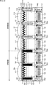
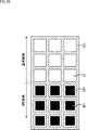
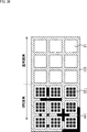
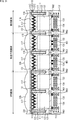
- FIG. 1 It is a figure which shows the schematic structure of the image pickup apparatus which concerns on this disclosure. It is a figure for demonstrating the pixel area of a pixel array part. It is a figure for demonstrating the arrangement of the pixel of the pixel array part. This is an example of the cross-sectional configuration of the pixels of the pixel array unit. This is an example of the cross-sectional configuration of the pixels of the pixel array unit. It is a figure which shows the other schematic structure of the image pickup apparatus. This is an example of the cross-sectional configuration of the pixels of the pixel array unit. This is an example of the cross-sectional configuration of the pixels of the pixel array unit. This is an example of the cross-sectional configuration of the pixels of the pixel array unit. This is an example of the cross-sectional configuration of the pixels of the pixel array unit.
- the cross-sectional structure of the image pickup device in the fifth embodiment It is an example of the plane configuration of the image pickup device in the fifth embodiment. It is an example of the cross-sectional structure of the image pickup device in the sixth embodiment. It is an example of the plane configuration of the image pickup device in the sixth embodiment. It is an example of the cross-sectional structure of the image pickup device in the 7th embodiment. It is an example of the cross-sectional structure of the image pickup device in the eighth embodiment. It is an example of the plane configuration of the image pickup device in the eighth embodiment. It is an example of the cross-sectional structure of the image pickup device in the 9th embodiment. It is an example of the plane configuration of the image pickup device in the ninth embodiment.
- FIG. 1 shows a schematic configuration of an image pickup apparatus including an image pickup device according to the present disclosure.
- the image pickup apparatus 1 of FIG. 1 has a pixel array unit 3 in which pixels 2 are arranged in a two-dimensional array on a semiconductor substrate 12 using, for example, silicon (Si) as a semiconductor, and a peripheral circuit unit around the pixel array unit 3. It is composed of.
- the peripheral circuit unit includes a vertical drive circuit 4, a column signal processing circuit 5, a horizontal drive circuit 6, an output circuit 7, a control circuit 8, and the like.
- Pixel 2 includes a photodiode as a photoelectric conversion element and a plurality of pixel transistors.
- the plurality of pixel transistors are composed of four MOS transistors, for example, a transfer transistor, a selection transistor, a reset transistor, and an amplification transistor.
- the pixel 2 can also have a shared pixel structure.
- This pixel sharing structure is composed of a plurality of photodiodes, a plurality of transfer transistors, one shared floating diffusion (floating diffusion region), and one shared other pixel transistor. That is, in the shared pixel, the photodiode and the transfer transistor constituting the plurality of unit pixels are configured by sharing the other pixel transistor.
- the control circuit 8 receives an input clock and data instructing an operation mode, etc., and outputs data such as internal information of the image pickup apparatus 1. That is, the control circuit 8 generates a clock signal or a control signal that serves as a reference for the operation of the vertical drive circuit 4, the column signal processing circuit 5, the horizontal drive circuit 6, etc., based on the vertical synchronization signal, the horizontal synchronization signal, and the master clock. do. Then, the control circuit 8 outputs the generated clock signal and control signal to the vertical drive circuit 4, the column signal processing circuit 5, the horizontal drive circuit 6, and the like.
- the vertical drive circuit 4 is composed of, for example, a shift register, selects a pixel drive wiring 10, supplies a pulse for driving the pixel 2 to the selected pixel drive wiring 10, and drives the pixel 2 in row units. That is, the vertical drive circuit 4 selectively scans each pixel 2 of the pixel array unit 3 in row units in the vertical direction, and a pixel signal based on the signal charge generated in the photoelectric conversion unit of each pixel 2 according to the amount of light received. Is supplied to the column signal processing circuit 5 through the vertical signal line 9.
- the column signal processing circuit 5 is arranged for each column of the pixel 2, and performs signal processing such as noise removal for each pixel string of the signal output from the pixel 2 for one row.
- the column signal processing circuit 5 performs signal processing such as CDS (Correlated Double Sampling) and AD conversion for removing fixed pattern noise peculiar to pixels.
- the horizontal drive circuit 6 is composed of, for example, a shift register, and by sequentially outputting horizontal scanning pulses, each of the column signal processing circuits 5 is sequentially selected, and a pixel signal is output from each of the column signal processing circuits 5 as a horizontal signal line. Output to 11.
- the output circuit 7 performs signal processing on the signals sequentially supplied from each of the column signal processing circuits 5 through the horizontal signal line 11 and outputs the signals.
- the output circuit 7 may, for example, perform only buffering, or may perform black level adjustment, column variation correction, various digital signal processing, and the like.
- the input / output terminal 13 exchanges signals with the outside.
- the image pickup apparatus 1 configured as described above is a CMOS image sensor called a column AD method in which a column signal processing circuit 5 that performs CDS processing and AD conversion processing is arranged for each pixel string.
- the image pickup device 1 is a back-illuminated MOS type image pickup device in which light is incident from the back surface side opposite to the front surface side of the semiconductor substrate 12 on which the pixel transistor is formed.
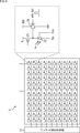
- FIG. 2 is a diagram showing a configuration example of the pixel array unit 3 of the image pickup apparatus 1.
- a normal pixel area 31 in which normal pixels are arranged and an OPB pixel area 32 in which OPB (optical black) pixels are arranged are arranged.
- the OPB pixel area 32 arranged at the upper end (in the figure) of the pixel array unit 3 is a light-shielding area that is shielded from light so as not to be incident.
- the normal pixel area 31 is an opening area that is not shielded from light.
- normal pixels (hereinafter, referred to as normal pixel 31) from which a pixel signal is read when an image is generated are arranged.
- the OPB pixel area 32 arranged in the upper light-shielding area is arranged with OPB pixels (hereinafter referred to as OPB pixel 32) used for reading a black level signal which is a pixel signal indicating a black level of an image. ..
- an effective unquestioned pixel area 33 in which the effective unquestioned pixels 33 are arranged is provided between the normal pixel area 31 and the OPB pixel area 32.
- the effective unquestioned pixel area 33 is an area in which the effective unquestioned pixel 33 in which the read pixel signal is not used for image generation is arranged.
- the effective and unquestioned pixel 33 mainly plays a role of ensuring the uniformity of the characteristics of the pixel signal of the normal pixel 31.
- the present technology described below can be applied to both the pixel array unit 3 shown in FIG. 2A and FIG. 2B. Further, even if the arrangement is other than the arrangement of the pixel array unit 3 shown in A of FIG. 2 and B of FIG. 2, the present technique described below can be applied.
- the OPB pixel area 32 has been shown as an example in which it is normally formed on one side of the pixel 31, but it can also be configured to be provided on 2 to 4 sides. Further, although the example in which the effective unquestioned pixel 33 is formed on one side of the normal pixel 31 is shown, the configuration may be provided on 2 to 4 sides.
- the normal pixel 31 arranged in the normal pixel area 31 can be a pixel that receives light in the visible light region, a pixel that receives infrared light (IR: Infrared), and the like. Further, the normal pixel 31 may be a pixel used for distance measurement.
- IR Infrared
- a case where a pixel that receives light in the visible light region and a pixel that receives infrared light are arranged in the pixel array unit 3 will be described as an example.
- a color image and an infrared image can be acquired at the same time.
- the pixel array unit 3 has R (Red) used for detecting red, as shown in FIG. ) Pixels, G (Green) pixels used for detecting green, B (Blue) pixels used for detecting blue, and IR pixels used for detecting infrared light are each provided in a two-dimensional grid pattern.
- FIG. 3 shows an example of the arrangement of the normal pixels 31 of the pixel array unit 3.
- the normal pixels 31 are arranged at a ratio of: 4. More specifically, the G pixels are arranged in a checkered pattern.
- the R pixels are arranged in the first column of the first row and the third column of the third row.
- the B pixel is arranged in the third column of the first row and the first column of the third row.
- the IR pixels are arranged at the remaining pixel positions. Then, the pattern of this pixel arrangement is repeatedly arranged in the row direction and the column direction on the pixel array unit 3.
- the pixel arrangement shown in FIG. 3 is an example, and other arrangements can be used.
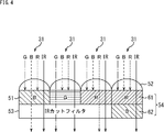
- FIG. 4 schematically shows a configuration example of a filter for each normal pixel 31.
- the B pixel, the G pixel, the R pixel, and the IR pixel are arranged from left to right.
- the on-chip lens 52, the color filter layer 51, and the IR cut filter 53 are laminated in this order from the incident side of the light.
- an R filter that transmits the wavelength range of red and infrared light is provided for the R pixel
- a G filter that transmits the wavelength range of green and infrared light is provided for the G pixel
- a B filter that transmits the wavelength range of blue and infrared light is provided for the B pixel.
- the IR cut filter 53 is a filter having a transmission band for near-infrared light in a predetermined range.
- the on-chip lens 52 and the IR filter 54 are laminated in order from the incident side of the light.
- the IR filter 54 is formed by stacking the R filter 61 and the B filter 62. By stacking the R filter 61 and the B filter 62, an IR filter 54 (that is, blue + red) that transmits light rays having a wavelength longer than 800 nm is formed.
- the R filter 61 is arranged on the on-chip lens 52 side and the B filter 62 is arranged on the lower side thereof, but the B filter 62 is arranged on the on-chip lens 52 side.
- the R filter 61 may be arranged below the R filter 61.
- pixels that receive light in the visible light region and pixels that receive infrared light can be arranged in the normal pixel region 31. Further, only the pixels that receive the light in the visible light region may be arranged in the normal pixel region 31. Further, this technique can be applied to the case where only the pixels that receive infrared light are arranged in the normal pixel region 31.
- FIG. 5 is a vertical cross-sectional view of the normal pixel 31.
- the normal pixel 31 described below will be described by taking the case of a back-illuminated type as an example, but the present technology can also be applied to the front-illuminated type.
- the normal pixel 31 shown in FIG. 5 has a PD (photodiode) 71 which is a photoelectric conversion element of each pixel formed inside the Si substrate 70.
- a P-type region 72 is formed on the light incident side (upper side and back surface side in the drawing) of the PD 71, and a flattening film 73 is formed on the lower layer of the P-type region 72.
- the boundary between the P-shaped region 72 and the flattening film 73 is defined as the back surface Si interface 75.
- a light-shielding film 74 is formed on the flattening film 73.
- the light-shielding film 74 is provided to prevent light from leaking to adjacent pixels, and is formed between adjacent PDs 71.
- the light-shielding film 74 is made of a metal material such as W (tungsten).
- An OCL (on-chip lens) 76 is formed on the flattening film 73 and on the back surface side of the Si substrate 70 to collect the incident light on the PD 71.
- a color filter layer may be formed between the OCL 76 and the flattening film 73. Further, the color filter layer can be the color filter layer 51 as shown in FIG.
- An active region (Pwell) 77 is formed on the opposite side of the PD71 on the light incident side (upper side in the figure, which is the surface side).
- an element separation region (hereinafter, referred to as STI (Shallow Trench Isolation)) 78 for separating pixel transistors and the like is formed.
- a wiring layer 79 is formed on the surface side (upper side of the drawing) of the Si substrate 70 and on the active region 77, and a plurality of transistors are formed on the wiring layer 79.
- FIG. 5 shows an example in which the transfer transistor 80 is formed.
- the transfer transistor (gate) 80 is formed of a vertical transistor. That is, in the transfer transistor (gate) 80, a vertical transistor trench 81 is opened, and a transfer gate (TG) 80 for reading charges from the PD 71 is formed therein.
- pixel transistors such as an amplifier (AMP) transistor, a selection (SEL) transistor, and a reset (RST) transistor are formed on the surface side of the Si substrate 70.
- AMP amplifier
- SEL selection
- RST reset
- a trench is usually formed between the pixels 31.
- This trench is described as DTI (Deep Trench Isolation) 82.
- the DTI 82 is formed in a shape that penetrates the Si substrate 70 in the depth direction (vertical direction in the figure, from the front surface to the back surface) between adjacent normal pixels 31.
- the DTI 82 also functions as a light-shielding wall between pixels so that unnecessary light does not leak to the adjacent normal pixels 31.
- a P-type solid phase diffusion layer 83 and an N-type solid phase diffusion layer 84 are formed in order from the DTI82 side toward the PD71.
- the P-type solid phase diffusion layer 83 is formed along the DTI 82 until it comes into contact with the back surface Si interface 75 of the Si substrate 70.
- the N-type solid phase diffusion layer 84 is formed along the DTI 82 until it comes into contact with the P-type region 72 of the Si substrate 70.
- the P-type solid phase diffusion layer 83 is formed until it contacts the back surface Si interface 75, but the N-type solid phase diffusion layer 84 does not contact the back surface Si interface 75, and the N-type solid phase diffusion layer 84 and the back surface Si interface. There is an interval between the 75.
- the PN junction region of the P-type solid phase diffusion layer 83 and the N-type solid phase diffusion layer 84 forms a strong electric field region and retains the electric charge generated by the PD 71.
- the P-type solid phase diffusion layer 83 and the N-type solid phase diffusion layer 84 formed along the DTI 82 form a strong electric field region, and the charges generated in the PD 71 can be retained. ..
- the N-type solid phase diffusion layer 84 is configured not to be in contact with the back surface Si interface 75 of the Si substrate 70, and is formed to be in contact with the P-type region 72 of the Si substrate 70 along the DTI 82. Has been done. With such a configuration, it is possible to prevent the pinning of the electric charge from being weakened, and it is possible to prevent the electric charge from flowing into the PD 71 and deteriorating the Dark characteristics.
- a side wall film 85 made of SiO2 is formed on the inner wall of the DTI 82, and a filler 86 made of polysilicon is embedded inside the side wall film 85.
- ⁇ Structure of unit pixel> Next, another specific structure of the normal pixels 31 arranged in a matrix in the normal pixel area 31 will be described.
- a pixel that receives infrared light can be arranged, and a pixel for measuring a distance to a subject using a signal obtained from the pixel can be arranged.
- the cross-sectional configuration of the normal pixel 31 arranged in the device (distance measuring device) that performs such distance measuring will be described.
- the ToF method includes a DirectToF (dToF) method and an IndirectToF (iToF) method.
- dToF DirectToF
- iToF IndirectToF
- a pixel for distance measurement by the dToF method is arranged as a normal pixel 31 will be described as an example.
- the DToF method is a method of directly measuring the distance from the time when the light is irradiated toward the subject and the time when the reflected light reflected from the subject is received.
- FIG. 6 is a diagram showing the configuration of the image pickup apparatus 1 when the normal pixels 31 are composed of DToF type pixels.
- the image pickup apparatus 1 includes a pixel array unit 3 and a bias voltage application unit 21.
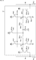
- the pixel array unit 3 is a light receiving surface that receives light collected by an optical system (not shown), and a plurality of SPAD pixels 2 are arranged in a matrix. As shown on the right side of FIG. 6, the SPAD pixel 2 includes a SPAD element 22, a p-type MOSFET (Metal-Oxide-Semiconductor Field-Effect Transistor) 23, and a CMOS inverter 24.
- CMOS inverter 24 Metal-Oxide-Semiconductor Field-Effect Transistor
- the SPAD element 22 forms an avalanche multiplying region by applying a large negative voltage VBD to the cathode, and can multiply the electrons generated by the incident of one photon to the avalanche.
- VBD negative voltage
- the p-type MOSFET 23 emits the multiplied electrons in the SPAD element 22 and performs quenching to return to the initial voltage.
- the CMOS inverter 24 outputs a light receiving signal (APDOUT) in which a pulse waveform is generated starting from the arrival time of one photon by shaping the voltage generated by the electrons multiplied by the SPAD element 22.
- the bias voltage application unit 21 applies a bias voltage to each of the plurality of SPAD pixels 2 arranged in the pixel array unit 3.
- a light receiving signal is output for each SPAD pixel 2 and supplied to a subsequent arithmetic processing unit (not shown).
- the arithmetic processing unit performs arithmetic processing for obtaining the distance to the subject based on the timing at which a pulse indicating the arrival time of one photon is generated in each received light signal, and obtains the distance for each SPAD pixel 2. Then, based on those distances, a distance image in which the distances to the subject detected by the plurality of SPAD pixels 2 are arranged in a plane is generated.
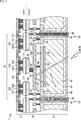
- FIG. 7 is a diagram showing a cross-sectional configuration example of the SPAD pixel 2.
- the image pickup apparatus 1 has a laminated structure in which a sensor substrate 25, a sensor side wiring layer 26, and a logic side wiring layer 27 are laminated, and is not shown with respect to the logic side wiring layer 27. It is configured by stacking logic circuit boards.
- the bias voltage application unit 21 of FIG. 6, the p-type MOSFET 23, the CMOS inverter 24, and the like are formed on the logic circuit board.
- the image pickup apparatus 1 forms the sensor side wiring layer 26 with respect to the sensor substrate 25, forms the logic side wiring layer 27 with respect to the logic circuit board, and then forms the sensor side wiring layer 26 and the logic side wiring layer 27.
- the sensor substrate 25 is, for example, a semiconductor substrate obtained by thinly slicing single crystal silicon, and the concentration of p-type or n-type impurities is controlled, and a SPAD element 22 is formed for each SPAD pixel 2. Further, in FIG. 7, the surface facing the lower side of the sensor substrate 25 is a light receiving surface that receives light, and the sensor side wiring layer 26 is laminated on the surface opposite to the light receiving surface.
- the sensor-side wiring layer 26 and the logic-side wiring layer 27 are formed with wiring for supplying a voltage applied to the SPAD element 22 and wiring for extracting electrons generated by the SPAD element 22 from the sensor board 25.
- the SPAD element 22 is composed of an N-well 41, a P-type diffusion layer 42, an N-type diffusion layer 43, a hole storage layer 44, a pinning layer 45, and a high-concentration P-type diffusion layer 46 formed on the sensor substrate 25. Then, in the SPAD element 22, the avalanche multiplying region 47 is formed by the depletion layer formed in the region where the P-type diffusion layer 42 and the N-type diffusion layer 43 are connected.
- the N-well 41 is formed by controlling the impurity concentration of the sensor substrate 25 to be n-type, and forms an electric field that transfers electrons generated by photoelectric conversion in the SPAD element 22 to the avalanche multiplication region 47.
- the impurity concentration of the sensor substrate 25 may be controlled to be p-type to form the P-well.
- the P-type diffusion layer 42 is a dense P-type diffusion layer (P +) formed on the back surface side (lower side of FIG. 7) with respect to the N-type diffusion layer 43 in the vicinity of the front surface of the sensor substrate 25, and is a SPAD. It is formed so as to cover almost the entire surface of the element 22.
- the N-type diffusion layer 43 is a dense N-type diffusion layer (N +) formed on the surface side (upper side of FIG. 7) with respect to the P-type diffusion layer 42 in the vicinity of the surface of the sensor substrate 25, and is a SPAD element. It is formed so as to cover almost the entire surface of 22. Further, a part of the N-type diffusion layer 43 is formed up to the surface of the sensor substrate 25 in order to connect to the contact electrode 90 for supplying a negative voltage for forming the avalanche multiplying region 47. It has a convex shape.
- the hole storage layer 44 is a P-type diffusion layer (P) formed so as to surround the side surface and the bottom surface of the N well 41, and stores holes. Further, the hole storage layer 44 is electrically connected to the anode of the SPAD element 22 and enables bias adjustment. As a result, the hole concentration of the hole storage layer 44 is strengthened, and the pinning including the pinning layer 45 is strengthened, so that, for example, the generation of dark current can be suppressed.
- P P-type diffusion layer
- the pinning layer 45 is a dense P-type diffusion layer (P +) formed on the outer surface of the hole storage layer 44 (the back surface of the sensor substrate 25 and the side surface in contact with the insulating film 49), and is similar to the hole storage layer 44. In addition, for example, the generation of dark current is suppressed.
- the high-concentration P-type diffusion layer 46 is a dense P-type diffusion layer (P ++) formed so as to surround the outer periphery of the N-well 41 in the vicinity of the surface of the sensor substrate 25, and the hole storage layer 44 is used as the anode of the SPAD element 22. It is used for connection with the contact electrode 91 for electrically connecting with.
- the avalanche multiplying region 47 is a high electric field region formed on the interface between the P-type diffusion layer 42 and the N-type diffusion layer 43 by a large negative voltage applied to the N-type diffusion layer 43, and is incident on the SPAD element 22. Multiplier the electron (e-) generated by one photon.
- each SPAD element 22 is insulated and separated by a double-structured interpixel separation portion 50 formed by a metal film 48 and an insulating film 49 formed between adjacent SPAD elements 22.
- the inter-pixel separation portion 50 is formed so as to penetrate from the back surface to the front surface of the sensor substrate 25.
- the metal film 48 is a film formed of a metal that reflects light (for example, tungsten or the like), and the insulating film 49 is a film having an insulating property such as SiO2.
- the inter-pixel separation portion 50 is formed by embedding the surface of the metal film 48 in the sensor substrate 25 so as to be covered with the insulating film 49, and the inter-pixel separation portion 50 is used to electrically connect the metal film 48 with the adjacent SPAD element 22. Targeted and optically separated.
- Contact electrodes 90 to 92, metal wiring 93 to 95, contact electrodes 96 to 98, and metal pads 99 to 100 are formed on the sensor side wiring layer 26.
- the contact electrode 90 connects the N-type diffusion layer 43 and the metal wiring 93, the contact electrode 91 connects the high-concentration P-type diffusion layer 46 and the metal wiring 94, and the contact electrode 92 is the metal film 48 and the metal. Connect to the wiring 95.
- the metal wiring 93 is formed wider than the avalanche multiplying region 47 so as to cover at least the avalanche multiplying region 47, as shown in FIG. 3, for example. Then, as shown by the white arrow in FIG. 7, the metal wiring 93 reflects the light transmitted through the SPAD element 22 to the SPAD element 22.
- the metal wiring 94 is formed so as to surround the outer periphery of the metal wiring 93 in a plan view and overlap with the high-concentration P-type diffusion layer 46.
- the metal wiring 95 is formed so as to be connected to the metal film 48 at the four corners of the SPAD pixel 2 in a plan view.
- the contact electrode 96 connects the metal wiring 93 and the metal pad 99
- the contact electrode 167 connects the metal wiring 94 and the metal pad 99
- the contact electrode 168 connects the metal wiring 95 and the metal pad 100. ..
- the metal pads 99 to 82 are used to electrically and mechanically join the metal pads 171 to 173 formed on the logic side wiring layer 27 by the metals (Cu) forming each of them.
- the logic side wiring layer 27 is formed with electrode pads 161 to 163, insulating layers 164, contact electrodes 165 to 170, and metal pads 171 to 173.
- the electrode pads 161 to 163 are used for connection with a logic circuit board (not shown), respectively, and the insulating layer 164 insulates the electrode pads 161 to 163 from each other.
- the contact electrodes 165 and 166 connect the electrode pads 161 and the metal pads 171, the contact electrodes 167 and 168 connect the electrode pads 162 and the metal pads 172, and the contact electrodes 169 and 170 connect the electrode pads 163 and the metal. Connect to the pad 173.
- the metal pad 171 is joined to the metal pad 99, the metal pad 172 is joined to the metal pad 99, and the metal pad 173 is joined to the metal pad 100.
- the electrode pad 161 is provided with the N-type diffusion layer 43 via the contact electrodes 165 and 166, the metal pad 171 and the metal pad 99, the contact electrode 96, the metal wiring 93, and the contact electrode 90. It is connected to the. Therefore, in the SPAD pixel 2, a large negative voltage applied to the N-type diffusion layer 43 can be supplied from the logic circuit board to the electrode pad 161.
- the electrode pad 162 is connected to the high-concentration P-type diffusion layer 46 via the contact electrodes 167 and 168, the metal pad 172, the metal pad 99, the contact electrode 97, the metal wiring 94, and the contact electrode 91. It has become. Therefore, in the SPAD pixel 2, the anode of the SPAD element 22 electrically connected to the hole storage layer 44 is connected to the electrode pad 162, so that the bias of the hole storage layer 44 can be adjusted via the electrode pad 162. can do.
- the electrode pad 163 is connected to the metal film 48 via the contact electrodes 169 and 170, the metal pad 173, the metal pad 100, the contact electrode 98, the metal wiring 95, and the contact electrode 92. There is. Therefore, in the SPAD pixel 2, the bias voltage supplied from the logic circuit board to the electrode pad 163 can be applied to the metal film 48.
- the metal wiring 93 is formed wider than the avalanche multiplying region 47 so as to cover at least the avalanche multiplying region 47, and the metal film 48 penetrates the sensor substrate 25. It is formed to do. That is, the SPAD pixel 2 is formed by a metal wiring 93 and a metal film 48 so as to have a reflection structure that surrounds all other than the light incident surface of the SPAD element 22. As a result, the SPAD pixel 2 can prevent the occurrence of optical crosstalk due to the effect of reflecting light by the metal wiring 93 and the metal film 48, and can improve the sensitivity of the SPAD element 22.
- the SPAD pixel 2 can adjust the bias by surrounding the side surface and the bottom surface of the N well 41 with the hole storage layer 44 and electrically connecting the hole storage layer 44 to the anode of the SPAD element 22. can. Further, the SPAD pixel 2 can form an electric field that assists the carrier in the avalanche multiplication region 47 by applying a bias voltage to the metal film 48 of the inter-pixel separation portion 50.
- the SPAD pixel 2 configured as described above can prevent the occurrence of crosstalk, and as a result of improving the sensitivity of the SPAD element 22, the characteristics can be improved. Further, such a SPAD pixel 2 can be used as a normal pixel 31.
- FIG. 8 is a cross-sectional view showing a configuration example of a normal pixel 31 arranged in the pixel array unit 3.
- the normal pixel 31 includes a semiconductor substrate 111 and a multilayer wiring layer 112 formed on the surface side (lower side in the drawing) thereof.
- the semiconductor substrate 111 is made of, for example, silicon (Si), and is formed with a thickness of, for example, 1 to 10 ⁇ m.
- a substrate made of a material such as InGaAs (iridium gallium arsenide) may be used.
- the photodiode PD is formed in pixel units by forming the N-type (second conductive type) semiconductor region 122 in pixel units in the P-type (first conductive type) semiconductor region 121. It is formed.
- the P-type semiconductor region 121 provided on both the front and back surfaces of the semiconductor substrate 111 also serves as a hole charge storage region for suppressing dark current.
- the upper surface of the semiconductor substrate 111 on the upper side in FIG. 8 is the back surface of the semiconductor substrate 111, which is the light incident surface on which light is incident.
- An antireflection film 113 is formed on the upper surface of the semiconductor substrate 111 on the back surface side.
- the antireflection film 113 has, for example, a laminated structure in which a fixed charge film and an oxide film are laminated, and for example, an insulating thin film having a high dielectric constant (High-k) by an ALD (Atomic Layer Deposition) method can be used.
- an insulating thin film having a high dielectric constant (High-k) by an ALD (Atomic Layer Deposition) method can be used.
- hafnium oxide (HfO2), aluminum oxide (Al2O3), titanium oxide (TiO2), STO (Strontium Titan Oxide) and the like can be used.
- the antireflection film 113 is configured by laminating a hafnium oxide film 123, an aluminum oxide film 124, and a silicon oxide film 125.
- a light-shielding film 115 is formed on the upper surface of the antireflection film 113, at the boundary portion 114 (hereinafter, also referred to as pixel boundary portion 114) of the adjacent normal pixels 31 of the semiconductor substrate 111, between the pixels that prevent the incident light from being incident on the adjacent pixels.
- a light-shielding film 115 is formed.
- the material of the inter-pixel light-shielding film 115 may be any material that blocks light, and for example, a metal material such as tungsten (W), aluminum (Al), or copper (Cu) can be used.
- the flattening film 116 is formed on the upper surface of the antireflection film 113 and the upper surface of the interpixel light-shielding film 115, for example, an insulating film such as silicon oxide (SiO2), silicon nitride (SiN), silicon oxynitride (SiON), or an insulating film. , Formed from organic materials such as resin.
- An on-chip lens 117 is formed for each pixel on the upper surface of the flattening film 116.
- the on-chip lens 117 is formed of, for example, a resin-based material such as a styrene-based resin, an acrylic-based resin, a styrene-acrylic copolymer resin, or a siloxane-based resin.
- the light focused by the on-chip lens 117 is efficiently incident on the photodiode PD.
- the pixel boundary portion 114 on the back surface side of the semiconductor substrate 111 has pixels adjacent to the depth direction of the semiconductor substrate 111 from the back surface side (on-chip lens 117 side) of the semiconductor substrate 111 to a predetermined depth in the substrate depth direction.
- An inter-pixel separation unit 131 that separates the two is formed.
- the bottom surface and the outer peripheral portion including the side wall of the inter-pixel separation portion 131 are covered with the hafnium oxide film 123 which is a part of the antireflection film 113.
- the inter-pixel separation unit 131 prevents the incident light from penetrating into the adjacent normal pixel 31, confine it in the own pixel, and prevents the incident light from leaking from the adjacent normal pixel 31.
- the silicon oxide film 125 and the inter-pixel separation portion 131 are simultaneously formed by embedding the silicon oxide film 125, which is the material of the uppermost layer of the antireflection film 113, in the trench (groove) dug from the back surface side. Therefore, the silicon oxide film 125, which is a part of the laminated film as the antireflection film 113, and the inter-pixel separation portion 131 are made of the same material, but they do not necessarily have to be the same.
- the material to be embedded in the trench (groove) dug from the back surface side as the inter-pixel separation portion 131 may be, for example, a metal material such as tungsten (W), aluminum (Al), titanium (Ti), titanium nitride (TiN) or the like.
- the stray diffusion regions FD1 and FD2 as charge storage portions that temporarily hold the charges transferred from the photodiode PD are formed by a high-concentration N-type semiconductor region (N-type diffusion region). It is formed.
- the multilayer wiring layer 112 is composed of a plurality of metal films M and an interlayer insulating film 132 between them.
- FIG. 8 shows an example composed of three layers of the first metal film M1 to the third metal film M3.
- the wiring 133 is formed on the first metal film M1, which is a predetermined metal film M, and the wiring 134 is formed on the second metal film M2. ing.
- the image pickup apparatus 1 arranges the semiconductor substrate 111, which is a semiconductor layer, between the on-chip lens 117 and the multilayer wiring layer 112, and emits incident light from the back surface side on which the on-chip lens 117 is formed. It has a back-illuminated structure that is incident on the PD.
- the normal pixel 31 includes two transfer transistors TRG1 and TRG2 for the photodiode PD provided in each pixel, and charges (electrons) generated by photoelectric conversion by the photodiode PD are transferred to a floating diffusion region. It is configured so that it can be distributed to FD1 or FD2.
- a pixel used for distance measurement provided with two transfer transistors TRG1 and TRG2, which may be referred to as a two-tap type, will be described as an example.
- the configuration of the pixel used for distance measurement is not limited to such a 2-tap type, and may be a pixel sometimes referred to as a 1-tap type including one transfer transistor.
- the configuration may be the same as that of the normal pixel 31 shown in FIG. That is, the normal pixel 31 having the configuration shown in FIG. 5 can also be used as a pixel for performing distance measurement.
- the pixel configuration used for distance measurement may be a pixel sometimes referred to as a 4-tap type including four transfer transistors. This technique is not limited to the number of transfer transistors included in one pixel, the distance measuring method, and the like, and can be applied.
- the normal pixel 31 shown in FIG. 8 has an inter-pixel separation portion 131 formed at the pixel boundary portion 114 to prevent incident light from penetrating into the adjacent normal pixel 31, confine it in its own pixel, and adjacent to the normal pixel 31. It prevents leakage of incident light from the normal pixel 31.
- the portion corresponding to the normal pixel 31 shown in FIG. 8 is designated by the same reference numeral, and the description of that portion will be omitted as appropriate.
- the PD upper region 153 located above the photodiode PD forming region of the semiconductor substrate 111 (P-type semiconductor region 121) has an uneven structure in which fine irregularities are formed. It has become.
- the antireflection film 151 formed on the upper surface of the semiconductor substrate 111 corresponding to the uneven structure of the PD upper region 153 is also formed by the uneven structure.
- the antireflection film 151 is composed of a laminate of a hafnium oxide film 123, an aluminum oxide film 124, and a silicon oxide film 125.
- the PD upper region 153 of the semiconductor region 121 into an uneven structure, it is possible to mitigate a sudden change in the refractive index at the interface of the substrate and reduce the influence of reflected light.
- the pixel-to-pixel separation section 131 formed by DTI dug from the back surface side (on-chip lens 117 side) of the semiconductor region 121 is slightly larger than the pixel-to-pixel separation section 131 of FIG. It is formed to a deep position.
- the depth in the substrate thickness direction in which the inter-pixel separation portion 131 is formed can be set to any depth in this way.
- FIG. 10 is a circuit in which normal pixels 31 are two-dimensionally arranged in the pixel array unit 3, and the normal pixels 31 are used as an image sensor having a configuration suitable for performing distance measurement as shown in FIG. 8 or 9. The configuration is shown.
- the normal pixel 31 includes a photodiode PD as a photoelectric conversion element. Further, the normal pixel 31 has two transfer transistors TRG, a floating diffusion region FD, an additional capacitance FDL, a switching transistor FDG, an amplification transistor AMP, a reset transistor RST, and a selection transistor SEL. Further, the normal pixel 31 has a charge discharge transistor OFG.
- transfer transistors TRG1 and TRG2 stray diffusion region FD1 and FD2, additional capacitance FDL1 and FDL2, switching transistors FDG1 and FDG2, amplification transistors AMP1 and AMP2, reset transistors RST1 and RST2, and selection transistors SEL1 and It is called like SEL2.
- the transfer transistor TRG, switching transistor FDG, amplification transistor AMP, selection transistor SEL, reset transistor RST, and charge emission transistor OFG are composed of, for example, an N-type MOS transistor.
- the transfer transistor TRG1 When the transfer drive signal TRG1g supplied to the gate electrode becomes active, the transfer transistor TRG1 becomes conductive in response to the transfer drive signal TRG1g, thereby transferring the charge stored in the photodiode PD to the floating diffusion region FD1.
- the transfer drive signal TRG2g supplied to the gate electrode becomes active, the transfer transistor TRG2 becomes conductive in response to the transfer drive signal TRG2g, thereby transferring the charge stored in the photodiode PD to the floating diffusion region FD2.
- the floating diffusion regions FD1 and FD2 are charge storage units that temporarily hold the charges transferred from the photodiode PD.
- the switching transistor FDG1 When the FD drive signal FDG1g supplied to the gate electrode becomes active, the switching transistor FDG1 becomes conductive in response to this, thereby connecting the additional capacitance FDL1 to the floating diffusion region FD1.
- the switching transistor FDG2 When the FD drive signal FDG2g supplied to the gate electrode becomes active, the switching transistor FDG2 becomes conductive in response to the FD drive signal FDG2g, thereby connecting the additional capacitance FDL2 to the floating diffusion region FD2.
- the additional capacitances FDL1 and FDL2 are formed by the wiring 134 of FIG.
- the reset transistor RST1 becomes conductive in response to the reset drive signal RSTg, thereby resetting the potential of the floating diffusion region FD1.
- the reset transistor RST2 becomes conductive in response to the reset drive signal RSTg, thereby resetting the potential of the floating diffusion region FD2.
- the reset transistors RST1 and RST2 are activated, the switching transistors FDG1 and FDG2 are also activated at the same time, and the additional capacitances FDL1 and FDL2 are also reset.
- the switching transistors FDG1 and FDG2 are activated, the floating diffusion region FD1 and the additional capacitance FDL1 are connected, and the floating diffusion region FD2 and the additional capacitance FDL2 are connected. To connect. This allows more charge to be stored at high illuminance.
- the vertical drive circuit 4 sets the switching transistors FDG1 and FDG2 in an inactive state, and separates the additional capacitances FDL1 and FDL2 from the stray diffusion regions FD1 and FD2, respectively. This makes it possible to increase the conversion efficiency.
- the charge discharge transistor OFG becomes conductive in response to the discharge drive signal OFG, thereby discharging the charge accumulated in the photodiode PD.
- the amplification transistor AMP1 is connected to a constant current source (not shown) by connecting the source electrode to the vertical signal line 9A via the selection transistor SEL1 to form a source follower circuit.
- the amplification transistor AMP2 is connected to a constant current source (not shown) by connecting the source electrode to the vertical signal line 9B via the selection transistor SEL2, and constitutes a source follower circuit.
- the selection transistor SEL1 is connected between the source electrode of the amplification transistor AMP1 and the vertical signal line 9A.
- the selection transistor SEL1 becomes conductive in response to the selection signal SEL1g, and outputs the detection signal VSL1 output from the amplification transistor AMP1 to the vertical signal line 9A.
- the selection transistor SEL2 is connected between the source electrode of the amplification transistor AMP2 and the vertical signal line 9B.
- the selection transistor SEL2 becomes conductive in response to the selection signal SEL2g, and outputs the detection signal VSL2 output from the amplification transistor AMP2 to the vertical signal line 9B.
- the transfer transistors TRG1 and TRG2 of the normal pixel 31, the switching transistors FDG1 and FDG2, the amplification transistors AMP1 and AMP2, the selection transistors SEL1 and SEL2, and the charge discharge transistor OFG are controlled by the vertical drive circuit 4.
- the additional capacitance FDL1 and FDL2 and the switching transistors FDG1 and FDG2 that control the connection thereof may be omitted, but by providing the additional capacitance FDL and using them properly according to the amount of incident light, high dynamics are achieved.
- the range can be secured.
- a reset operation for resetting the charge of the normal pixel 31 is performed on all pixels. That is, the charge discharge transistors OFG, the reset transistors RST1 and RST2, and the switching transistors FDG1 and FDG2 are turned on, and the stored charges of the photodiode PD, the stray diffusion regions FD1 and FD2, and the additional capacitances FDL1 and FDL2 are discharged. ..
- the transfer transistors TRG1 and TRG2 are driven alternately. That is, in the first period, the transfer transistor TRG1 is controlled to be on and the transfer transistor TRG2 is controlled to be off. In this first period, the electric charge generated by the photodiode PD is transferred to the stray diffusion region FD1. In the second period following the first period, the transfer transistor TRG1 is controlled to be off and the transfer transistor TRG2 is controlled to be on. In this second period, the electric charge generated by the photodiode PD is transferred to the stray diffusion region FD2. As a result, the electric charge generated by the photodiode PD is distributed to the floating diffusion regions FD1 and FD2 and accumulated.
- the transfer transistor TRG and the stray diffusion region FD on which the charge (electrons) obtained by photoelectric conversion is read out are also referred to as active taps.
- the transfer transistor TRG and the floating diffusion region FD on which the charge obtained by photoelectric conversion is not read out are also referred to as inactive taps.
- each normal pixel 31 of the pixel array unit 3 is sequentially selected in a line sequence.
- the selection transistors SEL1 and SEL2 are turned on.
- the electric charge accumulated in the floating diffusion region FD1 is output to the column signal processing circuit 5 via the vertical signal line 9A as the detection signal VSL1.
- the electric charge accumulated in the floating diffusion region FD2 is output to the column signal processing circuit 5 via the vertical signal line 9B as the detection signal VSL2.
- the reflected light normally received by the pixel 31 is delayed from the timing of irradiation by the light source according to the distance to the object. Since the distribution ratio of the electric charge accumulated in the two floating diffusion regions FD1 and FD2 changes depending on the delay time according to the distance to the object, the distribution ratio of the electric charge accumulated in the two floating diffusion regions FD1 and FD2 is used. , The distance to the object can be calculated.
- FIG. 11 is a plan view showing an arrangement example of the pixel circuit shown in FIG.
- the horizontal direction in FIG. 10 corresponds to the row direction (horizontal direction) of FIG. 1, and the vertical direction corresponds to the column direction (vertical direction) of FIG.
- a photodiode PD is formed in an N-type semiconductor region 122 in a region in the center of a rectangular normal pixel 31.
- a transfer transistor TRG1, a switching transistor FDG1, a reset transistor RST1, an amplification transistor AMP1, and a selection transistor SEL1 are linearly arranged along a predetermined side of four sides of a rectangular normal pixel 31 outside the photodiode PD.
- the transfer transistor TRG2, the switching transistor FDG2, the reset transistor RST2, the amplification transistor AMP2, and the selection transistor SEL2 are linearly arranged along the other side of the four sides of the rectangular normal pixel 31. ..
- the charge discharge transistor OFG is arranged on a side different from the two sides of the normal pixel 31 in which the transfer transistor TRG, the switching transistor FDG, the reset transistor RST, the amplification transistor AMP, and the selection transistor SEL are formed. ..
- the arrangement of the pixel circuits shown in FIG. 11 is not limited to this example, and may be other arrangements.
- a normal pixel area 31 and an OPB pixel area 32 are arranged in the pixel array unit 3. While the normal pixel area 31 is open, the OPB pixel area 32 is shielded from light.
- FIG. 12 shows a cross-sectional view of pixels in an area in which the normal pixel area 31 and the OPB pixel area 32 are arranged adjacent to each other.
- FIG. 12 shows an example in which two OPB pixels 32 are arranged on the left side of the figure and three normal pixels 31 are arranged on the right side.
- the normal pixel 31 shows the case where the normal pixel 31 has the uneven structure shown in FIG.
- the basic configuration of the OPB pixel 32 can be the same as that of the normal pixel 31. Since the OPB pixel region 32 is shielded from light, a light-shielding film 201 is formed on the on-chip lens 117 side of the OPB pixel 32 to shield the incident light.
- the OPB pixel 32 and the effective unquestioned pixel 33 can also be referred to as dummy pixels.
- the OPB pixel 32 and the effective unquestioned pixel 33 are pixels in which the read pixel signal is not used for image generation.
- the fact that the read pixel signal is not used for image generation can be said to be a pixel that is not displayed on the reproduced screen.
- the OPB pixel 32 shown in FIG. 12 shows a configuration including the on-chip lens 117, but the configuration of the OPB pixel 32 and the effective unquestioned pixel 33 (dummy pixel) may be such that the on-chip lens 117 is not provided. good. Further, the on-chip lens 117 may be formed in a deteriorated state such as being crushed.
- the dummy pixels may be configured not to be connected by the vertical signal line 9 (FIG. 1) when viewed in a plan view.
- the dummy pixel may be configured not to have a transistor equivalent to the transistor provided by the effective pixel (normal pixel 31).
- the transistors included in the normal pixel 31 have been described with reference to FIGS. 10 and 11, the normal pixel 31 includes a plurality of transistors, but the pixels having fewer transistors than the plurality of transistors included in the normal pixel 31 are referred to as dummy pixels. You can also do it.
- the dummy pixel has a configuration different from that of the normal pixel 31, and as shown in FIG. 12, has a light-shielding film 201 or among the elements (transistor, FD, OCL, etc.) of the normal pixel 31. At least one may have a different configuration.
- the configuration of the OPB pixel 32 is basically the same as that of the normal pixel 31, but the description will be continued by taking as an example the case where the configuration is different in that it has the light-shielding film 201.
- a structure having a concavo-convex structure in the PD upper region 153 such as the OPB pixel 32 shown in FIG. 12, will be described as an example, but the OPB pixel 32 is provided with the concavo-convex structure. It may be configured without.
- the light incident on the normal pixel 31 reaches, for example, the wiring in the multilayer wiring layer 112, and some light is reflected.
- the reflected light reaches the inter-pixel separation unit 131, is reflected, and is usually returned to the pixel 31, but there is also light that is transmitted and leaks to the adjacent OPB pixel 32.
- the inter-pixel separation unit 131 is composed of only a trench, the light reflected by the wiring in the multilayer wiring layer 112 passes through the inter-pixel separation unit 131 (trench) and is adjacent to the OPB pixel. There is a possibility that more light will leak into 32.
- the light reflected by the wiring in the multilayer wiring layer 112 may leak to the adjacent OPB pixel 32 through the P-type semiconductor region 121 in which the inter-pixel separation portion 131 is not formed. Further, the light leaked to the OPB pixel 32 may also leak to the adjacent OPB pixel 32.
- some distance measurement pixels used for distance measurement are designed to receive light of long wavelengths such as near infrared. Since the quantum efficiency of long-wavelength light is low on a silicon substrate, it tends to travel while being reflected inside the silicon substrate. That is, in the case of light having a long wavelength, there is a high possibility that more light leaks to adjacent pixels as described above.
- the OPB pixel 32 Since the OPB pixel 32 is used for reading a black level signal which is a pixel signal indicating the black level of an image, it is configured to block light and prevent light from entering. However, as described above, if the OPB pixel 32 leaks light from the adjacent normal pixel 31 or OPB pixel 32, a black level float may occur or variations may occur for each OPB pixel 32. , Black level setting accuracy may drop.
- the configuration of the image pickup device is the case of the configuration of the normal pixel 31 shown in FIG. 9, and the basic configuration of the OPB pixel 32 is the same as the configuration of the normal pixel 31 shown in FIG. The case will be described as an example.
- the embodiment described below can also be applied to an image pickup pixel that does not have the uneven structure as shown in FIG. Further, the embodiment described below will be described by taking as an example an image pickup device having a structure suitable for distance measurement shown in FIG. 9, but the present technology can also be applied to pixels for capturing a color image.
- FIG. 13 is a diagram showing a cross-sectional configuration example of the image pickup device according to the first embodiment.
- the image pickup device according to the first embodiment shown in FIG. 13 is compared with the image pickup device shown in FIG. 12. Since the inter-pixel separation unit 221 of the OPB pixel 32a shown in FIG. 13 is the same as the inter-pixel separation unit 131 of the OPB pixel 32 shown in FIG. 12, the description thereof will be omitted.
- the inter-pixel separation portion 221 of the OPB pixel 32a shown in FIG. 13 is configured to penetrate the semiconductor region 121 in the vertical direction in the figure.
- the inter-pixel separation portion 131 of the normal pixel 31 is formed non-penetratingly, whereas the inter-pixel separation portion 221 of the OPB pixel 32a has a penetrating configuration.
- the inter-pixel separation unit 131 of the normal pixel 31 arranged in the pixel array unit 3 and the inter-pixel separation unit 221 of the OPB pixel 32a have different configurations.
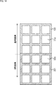
- FIG. 14 is a plan view of the normal pixel 31 and the OPB pixel 32a in the line segment ab of FIG.
- one rectangle represents a normal pixel 31 or OPB32a.
- One normal pixel 31 is surrounded by a non-penetrating interpixel separation portion 131.
- the pixel region 31 is formed with a non-penetrating pixel-to-pixel separation portion 131 formed in a grid pattern.
- One OPB pixel 32a is surrounded by a pixel-to-pixel separation portion 221 formed by penetration.
- the OPB pixel region 32a is formed with an inter-pixel separation portion 221 formed so as to penetrate in a grid pattern.
- the inter-pixel separation unit 221 of the OPB pixel 32a in the first embodiment By configuring the inter-pixel separation unit 221 of the OPB pixel 32a in the first embodiment to penetrate the semiconductor region 121, it is possible to suppress light leaking from the normal pixel 31.
- the OPB pixel 32 described with reference to FIG. 12 it is incident on the normal pixel 31 and reflected by the wiring of the multilayer wiring layer 112, and the lower part of the inter-pixel separation portion 131 formed in the OPB pixel 32 in FIG. There was a possibility that it would pass through the semiconductor region 121 in the above and enter the OPB pixel 32.
- the inter-pixel separation portion 221 is also formed in the semiconductor region 121 below the inter-pixel separation portion 131 formed in the OPB pixel 32 in FIG. 12, this region is defined. It is possible to prevent the reflected light that is transmitted and incident on the OPB pixel 32a.
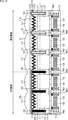
- FIG. 15 is a diagram showing a cross-sectional configuration example of the image pickup device according to the second embodiment.
- the image pickup device according to the second embodiment shown in FIG. 15 is compared with the image pickup device shown in FIG. Since the inter-pixel separation unit 241 of the OPB pixel 32b shown in FIG. 15 is the same as the inter-pixel separation unit 131 of the OPB pixel 32 shown in FIG. 12, the description thereof will be omitted.
- the inter-pixel separation portion 241 of the OPB pixel 32b shown in FIG. 15 is filled with a material that absorbs light.
- the material filled in the inter-pixel separation portion 241 of the OPB pixel 32b and the material filled in the inter-pixel separation portion 131 of the normal pixel 31 are different.
- the inter-pixel separation unit 131 of the normal pixel 31 returns the incident light and the reflected light reflected by the wiring in the multilayer wiring layer 112 to the PD 52, and is filled with a material suitable for confining the light in the PD 52. There is. In other words, the inter-pixel separation portion 131 of the normal pixel 31 is filled with a material (described as material A) having a higher reflection performance than the light-shielding performance.
- the inter-pixel separation portion 241 of the OPB pixel 32b is filled with a material suitable for suppressing light leakage from the adjacent normal pixel 31 or the OPB pixel 32b.
- the inter-pixel separation portion 241 of the OPB pixel 32b is filled with a material having a light-shielding performance higher than the reflection performance or a material having a high light-absorbing performance (described as the material B).
- the inter-pixel separation portion 241 of the OPB pixel 32b can be filled with a material having a high near-infrared light absorption coefficient or a material having a high reflection coefficient. Further, the inside of the inter-pixel separation unit 241 may be a single-layer film or a multilayer film.
- the material to be filled in the inter-pixel separation portion 241 of the OPB pixel 32b is, for example, SiO2 (silicon dioxide), Al (aluminum), W (tungsten), Cu (copper), Ti (titanium), TiN (titanium nitride), and the like. There is Ta (tantalu) and so on.
- the inter-pixel separation unit 131 of the normal pixel 31 arranged in the pixel array unit 3 and the inter-pixel separation unit 241 of the OPB pixel 32b have different configurations.
- FIG. 16 is a plan view of the normal pixel 31 and the OPB pixel 32b in the line segment ab of FIG.
- one rectangle represents a normal pixel 31 or OPB32b.
- One normal pixel 31 is surrounded by a pixel-to-pixel separation portion 131 filled with the material A.
- the inter-pixel separation portion 131 in which the material A is filled in a grid pattern is formed in the normal pixel region 31.
- One OPB pixel 32b is surrounded by a pixel-to-pixel separation portion 241 filled with the material B.
- the OPB pixel region 32b is formed with an inter-pixel separation portion 241 in which the material B is filled in a grid pattern.
- the inter-pixel separation portion 241 of the OPB pixel 32b in the second embodiment By configuring the inter-pixel separation portion 241 of the OPB pixel 32b in the second embodiment to be filled with the material B having a high light-shielding property, it is possible to suppress the light leaking from the normal pixel 31.
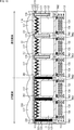
- FIG. 17 is a diagram showing a cross-sectional configuration example of the image pickup device according to the third embodiment.
- the image pickup device according to the third embodiment has a configuration in which the pixel array unit 3 is provided with a normal pixel area 31, an OPB pixel area 32, and an effective unquestioned pixel area 33. This is the case where the second embodiment is applied.
- the image pickup device according to the third embodiment shown in FIG. 17 is compared with the image pickup device shown in FIG.
- the same configuration as the inter-pixel separation unit 241 of the OPB pixel 32b shown in FIG. 15 is applied to the inter-pixel separation unit 261 of the effective unquestioned pixel 33 shown in FIG.
- the inter-pixel separation portion 261 of the effective unquestioned pixel 33c shown in FIG. 17 is filled with a material that absorbs light.
- the material filled in the inter-pixel separation portion 261 of the effective unquestioned pixel 33c and the material filled in the inter-pixel separation portion 131 of the normal pixel 31 are different.
- the inter-pixel separation portion 261 of the effective unquestioned pixel 33c is filled with a material suitable for suppressing leakage of light from the adjacent normal pixel 31 or the effective unquestioned pixel 33c.
- the material filled in the inter-pixel separation portion 261 of the effective unquestioned pixel 33c shown in FIG. 17 and the material filled in the inter-pixel separation portion 131 of the OPB pixel 32c are different.
- the basic configuration of the OPB pixel 32c has the same configuration as the normal pixel 31, but the basic configuration of the OPB pixel 32c may have the same configuration as the effective unquestioned pixel 33c. .. That is, the inter-pixel separation unit 131 of the OPB pixel 32c can be configured to be filled with a material having a high light-shielding property, like the inter-pixel separation unit 261 of the effective unquestioned pixel region 33c.
- the inter-pixel separation unit 131 of the OPB pixel 32c may have a structure different from that of the inter-pixel separation unit 261 of the effective unquestioned pixel 33c and the inter-pixel separation unit 131 of the normal pixel 31.
- the material to be filled in the inter-pixel separation portion 261 of the effective unquestioned pixel 33c is, for example, SiO2 (silicon dioxide), Al (aluminum), W (tungsten), Cu (copper), Ti (titanium), TiN (titanium nitride). , Ta (tantalu), etc.
- the inter-pixel separation unit 131 of the normal pixel 31 arranged in the pixel array unit 3 and the inter-pixel separation unit 261 of the effective unquestioned pixel 33c have different configurations.
- FIG. 18 is a plan view of the normal pixel 31, the OPB pixel 32c, and the effective unquestioned pixel 33c in the line segment ab of FIG.
- one quadrangle represents a normal pixel 31, OPB32c, or a valid and unquestioned pixel 33c.
- One normal pixel 31 is surrounded by a pixel-to-pixel separation portion 131 filled with the material A.
- the inter-pixel separation portion 131 in which the material A is filled in a grid pattern is formed in the normal pixel region 31.
- one OPB pixel 32c is surrounded by the inter-pixel separation portion 131 filled with the material A, like one normal pixel 31.
- the OPB pixel region 32c is formed with an inter-pixel separation portion 131 in which the material A is filled in a grid pattern.
- One effective unquestioned pixel 33c is surrounded by a pixel-to-pixel separation portion 261 filled with the material B.
- the effective unquestioned pixel region 33 is formed with an inter-pixel separation portion 261 in which the material B is filled in a grid pattern.
- the inter-pixel separation portion 261 of the effective unquestioned pixel 33c in the third embodiment With the material B having a high light-shielding property, it is possible to suppress the light leaking from the normal pixel 31. Further, since the light leaking to the effective unquestioned pixel 33c can be suppressed, the light leaking to the OPB pixel 32c adjacent to the effective unquestioned pixel 33c can also be suppressed.
- FIG. 19 is a diagram showing a cross-sectional configuration example of the image pickup device according to the fourth embodiment.
- the image pickup device according to the fourth embodiment shown in FIG. 19 is compared with the image pickup device shown in FIG. Since the inter-pixel separation portion 281 of the OPB pixel 32d shown in FIG. 19 is the same except that it is formed to a position deeper than the inter-pixel separation portion 241 of the OPB pixel 32b shown in FIG. The description is omitted.
- the inter-pixel separation unit 281 of the OPB pixel 32d in the fourth embodiment is formed to a position deeper than the inter-pixel separation unit 131 of the normal pixel 31, and is a material having a property of absorbing light more than the inter-pixel separation unit 131. Is filled.
- the inter-pixel separation unit 281 of the OPB pixel 32d has a configuration (penetrating trench) that penetrates the semiconductor substrate 111 as in the inter-pixel separation unit 221 (FIG. 13) of the OPB pixel 32a in the first embodiment.
- the inside of the trench may be filled with a material having a property of absorbing light.
- the OPB pixel 32d according to the fourth embodiment, it is possible to suppress the light leaking from the normal pixel 31 to the OPB pixel 32d and the light leaking from the adjacent OPB pixel 32d.
- FIG. 20 is a diagram showing a cross-sectional configuration example of the image pickup device according to the fifth embodiment.
- the image pickup device according to the fifth embodiment shown in FIG. 20 is compared with the image pickup device shown in FIG.
- the pixel-to-pixel separation section 301 of the OPB pixel 32e shown in FIG. 20 is the same except that the pixel-to-pixel separation section 301 of the OPB pixel 32b shown in FIG. 15 is formed thicker than the pixel-to-pixel separation section 241. Is omitted.
- the inter-pixel separation portion 301 of the OPB pixel 32e in the fifth embodiment is formed thicker than the inter-pixel separation portion 131 of the normal pixel 31, and is filled with a material having a property of absorbing light more than the inter-pixel separation portion 131. Has been done.
- the inter-pixel separation unit 301 of the OPB pixel 32e has a configuration (penetrating trench) that penetrates the semiconductor substrate 111 as in the inter-pixel separation unit 221 (FIG. 13) of the OPB pixel 32a in the first embodiment.
- the inside of the trench may be filled with a material having a property of absorbing light.
- FIG. 21 is a plan view of the normal pixel 31 and the OPB pixel 32e in the line segment ab of FIG. 20.
- one quadrangle represents a normal pixel 31 or an OPB pixel 32e.
- One normal pixel 31 is surrounded by a pixel-to-pixel separation portion 131 filled with the material A.
- One OPB pixel 32e is surrounded by the inter-pixel separation portion 301 filled with the material B, and the inter-pixel separation portion 301 is formed to be thicker (wider) than the inter-pixel separation portion 131.
- the OPB pixel region 32e is formed with an inter-pixel separation portion 301 in which the material B is filled in a wide grid pattern.
- the OPB pixel 32e it is possible to suppress the light leaking from the normal pixel 31 to the OPB pixel 32e and the light leaking from the adjacent OPB pixel 32e.
- FIG. 22 is a diagram showing a cross-sectional configuration example of the image pickup device according to the sixth embodiment.
- the image pickup device according to the sixth embodiment has a configuration in which the pixel array unit 3 is provided with a normal pixel area 31, an OPB pixel area 32, and an effective unquestioned pixel area 33. This is the case where the fifth embodiment is applied.
- the image pickup device according to the sixth embodiment shown in FIG. 22 is compared with the image pickup device shown in FIG. 20.
- the same configuration as the inter-pixel separation unit 301 of the OPB pixel 32e shown in FIG. 20 is the configuration provided in the inter-pixel separation unit 321 of the effective unquestioned pixel 33f shown in FIG. 20.
- the inter-pixel separation unit 321 of the effective unquestioned pixel 33f shown in FIG. 22 is shown in FIG.
- the difference is that the effective and unquestioned pixels 33c are formed thicker than the inter-pixel separation portion 261, and the other points are the same.
- the inter-pixel separation portion 321 of the effective unquestioned pixel 33f in the sixth embodiment is formed to be thicker than the inter-pixel separation portion 131 of the normal pixel 31, and is made of a material having a property of absorbing light more than the inter-pixel separation portion 131. It is filled.
- the inter-pixel separation unit 321 of the effective unquestioned pixel 33f has a configuration (penetrating trench) that penetrates the semiconductor substrate 111 as in the inter-pixel separation unit 221 (FIG. 13) of the OPB pixel 32a in the first embodiment.
- the inside of the trench may be filled with a material having a property of absorbing light.
- FIG. 23 is a plan view of the normal pixel 31, the OPB pixel 32f, and the effective unquestioned pixel 33f in the line segment ab of FIG. 22.
- one quadrangle represents a normal pixel 31, an OPB pixel 32f, or an effective unquestioned pixel 33f.
- One normal pixel 31 is surrounded by a pixel-to-pixel separation portion 131 filled with the material A.
- one OPB pixel 32f is surrounded by the inter-pixel separation portion 131 filled with the material A, like one normal pixel 31.
- the OPB pixel region 32f is formed with an inter-pixel separation portion 131 in which the material A is filled in a grid pattern.
- One effective unquestioned pixel 33f is surrounded by the inter-pixel separation portion 321 filled with the material B, and the inter-pixel separation portion 321 is formed to be thicker (wider) than the inter-pixel separation portion 131. ..
- the OPB pixel region 32f is formed with an inter-pixel separation portion 321 in which the material B is filled in a wide grid pattern.
- the effective unquestioned pixel 33f in the sixth embodiment it is possible to suppress the light leaking from the normal pixel 31 to the effective unquestioned pixel 33f and the light leaking from the adjacent effective unquestioned pixel 33f. Further, it is possible to suppress the leakage of light from the effective and unquestioned pixel 33f to the OPB pixel 32f.
- FIG. 24 is a diagram showing a cross-sectional configuration example of the image pickup device according to the seventh embodiment.
- the configuration of the image pickup device in the seventh embodiment is basically the same as that of the image pickup device in the second embodiment.
- the light-shielding film 341 of the OPB pixel 32g in the seventh embodiment shown in FIG. 24 is formed of the same material as the inter-pixel separation portion 241. Other points are the same.
- the process at the time of manufacturing can be reduced, and the cost can be reduced.
- the seventh embodiment is combined with the second embodiment has been described as an example, but it may be combined with the OPB pixel 32d (FIG. 19) in the fourth embodiment. , May be combined with the OPB pixel 32e (FIG. 20) in the fifth embodiment.
- the OPB pixel 32g according to the seventh embodiment it is possible to suppress the light leaking from the normal pixel 31 to the OPB pixel 32g and the light leaking from the adjacent OPB pixel 32g.
- FIG. 25 is a diagram showing a cross-sectional configuration example of the image pickup device according to the eighth embodiment.
- the image pickup device according to the eighth embodiment shown in FIG. 25 is compared with the image pickup device shown in FIG.
- the image pickup device shown in FIG. 25 is different from the image pickup device shown in FIG. 12 in that the 0th metal film M0 is newly added, and the other points are the same. The description thereof will be omitted.
- the 0th metal film M0 is provided between the first metal film M1 and the semiconductor substrate 111.
- a light-shielding member 401 is provided in the region of the OPB pixel 32h in the 0th metal film M0.
- metal wiring such as aluminum is formed as a light-shielding member 401.
- FIG. 26 is a plan view of the normal pixel 31 and the OPB pixel 32h in the line segment ab of FIG. 25.
- one quadrangle represents a normal pixel 31 or an OPB pixel 32h.
- One normal pixel 31 and one OPB pixel 32 are each surrounded by a pixel-to-pixel separation portion 131 filled with the material A.
- FIG. 26 also shows a light-shielding member 401.
- the light-shielding member 401 is formed in a region where at least a part overlaps with a region where the photodiode PD of the OPB pixel 32 is formed in a plan view.
- the same material as the material filled in the inter-pixel separation portion of the OPB pixel 32 in the above-described embodiment can be used.
- the light-shielding member 401 transmits the light incident on the semiconductor substrate 111 from the light incident surface via the on-chip lens 117 and transmitted through the semiconductor substrate 111 without being photoelectrically converted in the semiconductor substrate 111 to the semiconductor substrate 111.
- the light is shielded by the nearest 0th metal film M0, and the light is prevented from penetrating into the 1st metal film M1 and the 2nd metal film M3 below it. Due to this shading function, the light that has passed through the semiconductor substrate 111 without being photoelectrically converted in the semiconductor substrate 111 is scattered by the metal film M below the 0th metal film M0 and is incident on the neighboring pixels. Can be suppressed. This makes it possible to prevent erroneous detection of light by nearby pixels.
- the light-shielding member 401 also has a function of absorbing the light leaked from the adjacent normal pixel 31 or the OPB pixel 32h by the light-shielding member 401 and preventing the light from being re-entered into the photodiode PD of the OPB pixel 32h. Have.
- the OPB pixel 32h according to the eighth embodiment, it is possible to suppress the light leaking from the normal pixel 31 to the OPB pixel 32h and the light leaking from the adjacent OPB pixel 32h.
- FIG. 27 is a diagram showing a cross-sectional configuration example of the image pickup device according to the ninth embodiment.
- the image pickup device according to the ninth embodiment shown in FIG. 27 has a configuration in which the configuration of the OPB pixel 32h including the light-shielding member 401 according to the eighth embodiment is applied to the effective unquestioned pixel 33i.
- the image pickup device according to the ninth embodiment shown in FIG. 27 is also provided with the 0th metal film M0 between the first metal film M1 and the semiconductor substrate 111, similarly to the image pickup device according to the eighth embodiment. ing. Further, a light-shielding member 421 is provided in the region of the effective unquestioned pixel 33i in the 0th metal film M0.
- metal wiring such as aluminum or aluminum is formed as a light-shielding member 401.
- FIG. 28 is a plan view of the normal pixel 31, the OPB pixel 32i, and the effective unquestioned pixel 33i in the line segment ab of FIG. 27.
- one quadrangle represents a normal pixel 31, an OPB pixel 32i, or an effective unquestioned pixel 33i.
- One normal pixel 31, one OPB pixel 32i, and one effective unquestioned pixel 33i are each surrounded by a pixel-to-pixel separation portion 131 filled with a material A.
- FIG. 26 also shows a light-shielding member 421.
- the light-shielding member 421 is formed in a region where at least a part thereof overlaps with a region where the photodiode PD of the effective unquestioned pixel 33i is formed in a plan view.
- the effective unquestioned pixel 33i it is possible to suppress the light leaking from the normal pixel 31 to the effective unquestioned pixel 33i and the light leaking from the adjacent effective unquestioned pixel 33i. In addition, the light leaking from the effective unquestioned pixel 33i to the OPB pixel 32i can also be suppressed.
- FIG. 29 is a diagram showing a cross-sectional configuration example of the image pickup device according to the tenth embodiment.
- the image pickup device according to the eighth embodiment described above and the image pickup device according to the ninth embodiment are provided with the 0th metal film M0, and the light-shielding member 401 (421) is provided on the 0th metal film M0. An example is shown.
- the light-shielding member corresponding to the light-shielding member 401 (421) may be provided on a layer other than the 0th metal film M0.
- the image pickup device is provided with a light-shielding member 441 in the contact layer.
- the contact layer is the surface side of the semiconductor substrate 111 on which the multilayer wiring layer 112 is formed, and is a layer on which the two transfer transistors TRG1 and TRG2 are formed.
- a light-shielding member 421 may be formed in a region of the contact layer where no contact is provided.
- a light-shielding member 421 is provided on the contact layer of the OPB pixel 32j.
- the light-shielding member 421 is not provided on the contact layer of the normal pixel 31.
- the light-shielding member 421 By providing the light-shielding member 421 on the contact layer, it is not necessary to form the 0th metal film M0, so that the step for forming the 0th metal film M0 can be omitted. Further, since the light-shielding member 421 can be formed at the same time as the contact in the step of forming the contact on the contact layer, the light-shielding member 421 can be manufactured without increasing the number of steps.
- FIG. 30 is a plan view of the normal pixel 31 and the OPB pixel 32h in the line segment ab of FIG. 29.
- one rectangle represents a normal pixel 31 or an OPB pixel 32h.
- One normal pixel 31 and one OPB pixel 32 are each surrounded by a pixel-to-pixel separation portion 131 filled with the material A.
- FIG. 30 also shows a light-shielding member 421.
- the light-shielding member 421 is formed in a region where at least a part overlaps with a region where the photodiode PD of the OPB pixel 32 is formed in a plan view.
- the light-shielding member 421 formed in the region of the photodiode PD shows an example in which the quadrangles are arranged in 3 ⁇ 3.
- the shape of the light-shielding member 421 is not limited to a quadrangular shape, and may be a shape other than a quadrangular shape, for example, a circular shape or a polygonal shape. Further, the arrangement is not limited to 3 ⁇ 3, and may be arranged at a position that does not affect the contact. Further, the light-shielding member 421 may be formed in the same shape (shape and size) as the contact, or may be formed in a different shape.
- the light-shielding member 421 may also be formed below the inter-pixel separation portion 131 surrounding the OPB pixel 32j. In a plan view, for example, as shown in FIG. 30, a light-shielding member 421 is also provided in a region located below the inter-pixel separation portion 131. In the example shown in FIG. 30, an example in which the light-shielding member 421 is formed in a different shape depending on the location is shown.
- the light-shielding member 421 may be formed in a part of the lower region of the inter-pixel separation portion 131, or may be formed so as to surround the OPB pixel 32j like the inter-pixel separation portion 131.
- the shape, size, arrangement position, etc. of the light-shielding member 421 may be arranged so that a predetermined pattern is repeated or arranged independently of any pattern.
- the OPB pixel 32j according to the tenth embodiment, it is possible to suppress the light leaking from the normal pixel 31 to the OPB pixel 32j and the light leaking from the adjacent OPB pixel 32j.
- FIG. 31 is a diagram showing a cross-sectional configuration example of the image pickup device according to the eleventh embodiment.
- the image pickup device according to the eleventh embodiment shown in FIG. 31 has a configuration in which the configuration of the OPB pixel 32j provided with the light-shielding member 421 according to the tenth embodiment is applied to the effective unquestioned pixel 33k.
- the image pickup device according to the eleventh embodiment shown in FIG. 31 is also provided with the light-shielding member 461 in the contact layer, similarly to the image pickup device according to the tenth embodiment.
- the light-shielding member 461 is formed in the contact layer of the effective unquestioned pixel 33k.
- the light-shielding member 441 may also be formed on the OPB pixel 32k as in the tenth embodiment.
- the inter-pixel separation portion of the OPB pixel 32 may be filled with a material different from that of the inter-pixel separation portion 131 of the normal pixel 31, and a light-shielding member may be provided at the bottom of the OPB pixel 32.
- the inter-pixel separation portion of the effective unquestioned pixel 33 may be configured to be filled with a material different from the inter-pixel separation portion 131 of the normal pixel 31, and a light-shielding member may be provided below the effective unquestioned pixel 33.
- FIG. 32 shows an image pickup device of an embodiment in which the OPB pixel 32b (FIG. 15) in the second embodiment and the OPB pixel 32j in the tenth embodiment are combined.
- the OPB pixel 32m in the twelfth embodiment shown in FIG. 32 includes a pixel-to-pixel separation portion 241 filled with a material having a high light-shielding property, and a light-shielding member 441 is provided in the contact layer.
- the inter-pixel separation unit 131 of the normal pixel 31 and the inter-pixel separation unit of the OPB pixel 32 have different configurations. By doing so, the light leaking to the OPB pixel 32 can be suppressed, and the accuracy of setting the black level can be improved.
- the inter-pixel separation portion of the OPB pixel 32 may be made of a material or configuration capable of preventing light leakage from adjacent pixels more than the inter-pixel separation portion 131 of the normal pixel 31. , The light leaking to the OPB pixel 32 can be suppressed, and the accuracy of setting the black level can be improved.
- the image sensor leaks into the OPB pixel 32.
- the light can be suppressed and the accuracy of setting the black level can be improved.
- FIG. 33 is a block diagram showing a configuration example of a distance measuring module that outputs distance measurement information using the above-mentioned image pickup apparatus 1.
- the ranging module 500 includes a light emitting unit 511, a light emitting control unit 512, and a light receiving unit 513.
- the light emitting unit 511 has a light source that emits light having a predetermined wavelength, and emits irradiation light whose brightness fluctuates periodically to irradiate an object.
- the light emitting unit 511 has a light emitting diode that emits infrared light having a wavelength in the range of 780 nm to 1000 nm as a light source, and irradiates in synchronization with the light emission control signal CLKp of a square wave supplied from the light emission control unit 512. Generates light.
- the emission control signal CLKp is not limited to a rectangular wave as long as it is a periodic signal.
- the light emission control signal CLKp may be a sine wave.
- the light emission control unit 512 supplies the light emission control signal CLKp to the light emission unit 511 and the light receiving unit 513, and controls the irradiation timing of the irradiation light.
- the frequency of this emission control signal CLKp is, for example, 20 megahertz (MHz).
- the frequency of the light emission control signal CLKp is not limited to 20 MHz (MHz) and may be 5 MHz (MHz) or the like.
- the light receiving unit 513 receives the reflected light reflected from the object, calculates the distance information for each pixel according to the light receiving result, and stores the depth value corresponding to the distance to the object (subject) as the pixel value. Generate and output.
- an image pickup device 1 having a pixel structure according to any one of the above-described embodiments is used.
- the image pickup device 1 as the light receiving unit 513 obtains distance information from the signal intensity according to the charge distributed to the floating diffusion region FD1 or FD2 of each pixel of the pixel array unit 3 based on the light emission control signal CLKp. Calculated for each.
- the number of taps of the pixel may be the above-mentioned 4 taps or the like.
- the image pickup device 1 having the above-mentioned pixel structure can be incorporated as the light receiving unit 513 of the distance measurement module 500 that obtains and outputs the distance information to the subject by the indirect ToF method. This makes it possible to improve the distance measuring characteristics of the distance measuring module 500.
- the image pickup device 1 can be applied to a distance measurement module as described above, and is also applicable to various electronic devices such as an image pickup device such as a digital still camera and a digital video camera having a distance measurement function, and a smartphone having a distance measurement function. can do.
- FIG. 34 is a block diagram showing a configuration example of a smartphone as an electronic device to which the present technology is applied.
- the smartphone 601 has a distance measuring module 602, an image pickup device 603, a display 604, a speaker 605, a microphone 606, a communication module 607, a sensor unit 608, a touch panel 609, and a control unit 610. It is configured to be connected via. Further, the control unit 610 has functions as an application processing unit 621 and an operation system processing unit 622 by executing a program by the CPU.
- the distance measuring module 500 of FIG. 33 is applied to the distance measuring module 602.
- the distance measurement module 602 is arranged in front of the smartphone 601 and performs distance measurement for the user of the smartphone 601 to measure the depth value of the surface shape of the user's face, hand, finger, etc. as the distance measurement result. Can be output as.
- the image pickup device 603 is arranged in front of the smartphone 601 and takes an image of the user of the smartphone 601 as a subject to acquire an image of the user. Although not shown, the image pickup device 603 may be arranged on the back surface of the smartphone 601.
- the display 604 displays an operation screen for processing by the application processing unit 621 and the operation system processing unit 622, an image captured by the image pickup device 603, and the like.
- the communication module 607 is a network via a communication network such as the Internet, a public telephone network, a wide area communication network for wireless mobiles such as so-called 4G lines and 5G lines, and a WAN (Wide Area Network) and LAN (Local Area Network). Performs short-range wireless communication such as communication, Bluetooth (registered trademark), and NFC (Near Field Communication).
- the sensor unit 608 senses speed, acceleration, proximity, etc., and the touch panel 609 acquires a user's touch operation on the operation screen displayed on the display 604.
- the application processing unit 621 performs processing for providing various services by the smartphone 601.
- the application processing unit 621 can create a face by computer graphics that virtually reproduces the user's facial expression based on the depth value supplied from the distance measuring module 602, and can perform a process of displaying the face on the display 604. .
- the application processing unit 621 can perform a process of creating, for example, three-dimensional shape data of an arbitrary three-dimensional object based on the depth value supplied from the distance measuring module 602.
- the operation system processing unit 622 performs processing for realizing the basic functions and operations of the smartphone 601. For example, the operation system processing unit 622 can perform a process of authenticating the user's face and unlocking the smartphone 601 based on the depth value supplied from the distance measuring module 602. Further, the operation system processing unit 622 performs a process of recognizing a user's gesture based on the depth value supplied from the distance measuring module 602, and performs a process of inputting various operations according to the gesture. Can be done.
- the smartphone 601 configured in this way, by applying the above-mentioned distance measuring module 500 as the distance measuring module 602, for example, the distance to a predetermined object can be measured and displayed, or the tertiary of the predetermined object can be measured and displayed. It is possible to perform processing such as creating and displaying original shape data.
- the technology according to the present disclosure can be applied to various products.
- the technology according to the present disclosure is realized as a device mounted on a moving body of any kind such as an automobile, an electric vehicle, a hybrid electric vehicle, a motorcycle, a bicycle, a personal mobility, an airplane, a drone, a ship, and a robot. You may.
- FIG. 35 is a block diagram showing a schematic configuration example of a vehicle control system, which is an example of a mobile control system to which the technique according to the present disclosure can be applied.
- the vehicle control system 12000 includes a plurality of electronic control units connected via the communication network 12001.
- the vehicle control system 12000 includes a drive system control unit 12010, a body system control unit 12020, an outside information detection unit 12030, an in-vehicle information detection unit 12040, and an integrated control unit 12050.
- a microcomputer 12051, an audio image output unit 12052, and an in-vehicle network I / F (Interface) 12053 are shown as a functional configuration of the integrated control unit 12050.
- the drive system control unit 12010 controls the operation of the device related to the drive system of the vehicle according to various programs.
- the drive system control unit 12010 has a driving force generator for generating the driving force of the vehicle such as an internal combustion engine or a driving motor, a driving force transmission mechanism for transmitting the driving force to the wheels, and a steering angle of the vehicle. It functions as a control device such as a steering mechanism for adjusting and a braking device for generating braking force of the vehicle.
- the body system control unit 12020 controls the operation of various devices mounted on the vehicle body according to various programs.
- the body system control unit 12020 functions as a keyless entry system, a smart key system, a power window device, or a control device for various lamps such as headlamps, back lamps, brake lamps, turn signals or fog lamps.
- the body system control unit 12020 may be input with radio waves transmitted from a portable device that substitutes for the key or signals of various switches.
- the body system control unit 12020 receives inputs of these radio waves or signals and controls a vehicle door lock device, a power window device, a lamp, and the like.
- the outside information detection unit 12030 detects information outside the vehicle equipped with the vehicle control system 12000.
- the image pickup unit 12031 is connected to the vehicle outside information detection unit 12030.
- the vehicle outside information detection unit 12030 causes the image pickup unit 12031 to capture an image of the outside of the vehicle and receives the captured image.
- the vehicle outside information detection unit 12030 may perform object detection processing or distance detection processing such as a person, a vehicle, an obstacle, a sign, or a character on the road surface based on the received image.
- the image pickup unit 12031 is an optical sensor that receives light and outputs an electric signal according to the amount of the light received.
- the image pickup unit 12031 can output an electric signal as an image or can output it as distance measurement information. Further, the light received by the image pickup unit 12031 may be visible light or invisible light such as infrared light.
- the in-vehicle information detection unit 12040 detects the in-vehicle information.
- a driver state detection unit 12041 that detects the state of the driver is connected to the in-vehicle information detection unit 12040.
- the driver state detection unit 12041 includes, for example, a camera that images the driver, and the in-vehicle information detection unit 12040 determines the degree of fatigue or concentration of the driver based on the detection information input from the driver state detection unit 12041. It may be calculated, or it may be determined whether the driver has fallen asleep.
- the microcomputer 12051 calculates the control target value of the driving force generator, the steering mechanism, or the braking device based on the information inside and outside the vehicle acquired by the vehicle exterior information detection unit 12030 or the vehicle interior information detection unit 12040, and the drive system control unit.
- a control command can be output to 12010.
- the microcomputer 12051 realizes ADAS (Advanced Driver Assistance System) functions including vehicle collision avoidance or impact mitigation, follow-up driving based on inter-vehicle distance, vehicle speed maintenance driving, vehicle collision warning, vehicle lane deviation warning, and the like. It is possible to perform cooperative control for the purpose of.
- ADAS Advanced Driver Assistance System
- the microcomputer 12051 controls the driving force generating device, the steering mechanism, the braking device, and the like based on the information around the vehicle acquired by the vehicle exterior information detection unit 12030 or the vehicle interior information detection unit 12040. It is possible to perform coordinated control for the purpose of automatic driving that runs autonomously without depending on the operation.
- the microcomputer 12051 can output a control command to the body system control unit 12030 based on the information outside the vehicle acquired by the vehicle outside information detection unit 12030.
- the microcomputer 12051 controls the headlamps according to the position of the preceding vehicle or the oncoming vehicle detected by the outside information detection unit 12030, and performs cooperative control for the purpose of anti-glare such as switching the high beam to the low beam. It can be carried out.
- the audio image output unit 12052 transmits an output signal of at least one of audio and image to an output device capable of visually or audibly notifying information to the passenger or the outside of the vehicle.
- an audio speaker 12061, a display unit 12062, and an instrument panel 12063 are exemplified as output devices.
- the display unit 12062 may include, for example, at least one of an onboard display and a head-up display.
- FIG. 36 is a diagram showing an example of the installation position of the image pickup unit 12031.
- the image pickup unit 12031 has image pickup units 12101, 12102, 12103, 12104, and 12105.
- the image pickup units 12101, 12102, 12103, 12104, 12105 are provided at positions such as, for example, the front nose, side mirrors, rear bumpers, back doors, and the upper part of the windshield in the vehicle interior of the vehicle 12100.
- the image pickup unit 12101 provided in the front nose and the image pickup section 12105 provided in the upper part of the windshield in the vehicle interior mainly acquire an image in front of the vehicle 12100.
- the image pickup units 12102 and 12103 provided in the side mirror mainly acquire images of the side of the vehicle 12100.
- the image pickup unit 12104 provided in the rear bumper or the back door mainly acquires an image of the rear of the vehicle 12100.
- the image pickup unit 12105 provided on the upper part of the windshield in the vehicle interior is mainly used for detecting a preceding vehicle, a pedestrian, an obstacle, a traffic light, a traffic sign, a lane, or the like.
- FIG. 36 shows an example of the shooting range of the imaging units 12101 to 12104.
- the imaging range 12111 indicates the imaging range of the imaging unit 12101 provided on the front nose
- the imaging ranges 12112 and 12113 indicate the imaging range of the imaging units 12102 and 12103 provided on the side mirrors, respectively
- the imaging range 12114 indicates the imaging range.
- the imaging range of the imaging unit 12104 provided on the rear bumper or the back door is shown. For example, by superimposing the image data captured by the image pickup units 12101 to 12104, a bird's-eye view image of the vehicle 12100 can be obtained.
- At least one of the image pickup units 12101 to 12104 may have a function of acquiring distance information.
- at least one of the image pickup units 12101 to 12104 may be a stereo camera including a plurality of image pickup elements, or may be an image pickup element having pixels for phase difference detection.
- the microcomputer 12051 has a distance to each three-dimensional object in the image pickup range 12111 to 12114 based on the distance information obtained from the image pickup unit 12101 to 12104, and a temporal change of this distance (relative speed with respect to the vehicle 12100).
- a predetermined speed for example, 0 km / h or more
- the microcomputer 12051 can set an inter-vehicle distance to be secured in advance in front of the preceding vehicle, and can perform automatic brake control (including follow-up stop control), automatic acceleration control (including follow-up start control), and the like. In this way, it is possible to perform coordinated control for the purpose of automatic driving or the like in which the vehicle travels autonomously without depending on the operation of the driver.
- the microcomputer 12051 converts three-dimensional object data related to a three-dimensional object into two-wheeled vehicles, ordinary vehicles, large vehicles, pedestrians, electric poles, and other three-dimensional objects based on the distance information obtained from the image pickup units 12101 to 12104. It can be classified and extracted and used for automatic avoidance of obstacles. For example, the microcomputer 12051 distinguishes obstacles around the vehicle 12100 into obstacles that are visible to the driver of the vehicle 12100 and obstacles that are difficult to see. Then, the microcomputer 12051 determines the collision risk indicating the risk of collision with each obstacle, and when the collision risk is equal to or higher than the set value and there is a possibility of collision, the microcomputer 12051 via the audio speaker 12061 or the display unit 12062. By outputting an alarm to the driver and performing forced deceleration and avoidance steering via the drive system control unit 12010, driving support for collision avoidance can be provided.
- At least one of the image pickup units 12101 to 12104 may be an infrared camera that detects infrared rays.
- the microcomputer 12051 can recognize a pedestrian by determining whether or not a pedestrian is present in the captured image of the imaging unit 12101 to 12104.
- pedestrian recognition is, for example, a procedure for extracting feature points in an image captured by an image pickup unit 12101 to 12104 as an infrared camera, and pattern matching processing is performed on a series of feature points indicating the outline of an object to determine whether or not the pedestrian is a pedestrian. It is done by the procedure to determine.
- the audio image output unit 12052 determines the square contour line for emphasizing the recognized pedestrian.
- the display unit 12062 is controlled so as to superimpose and display. Further, the audio image output unit 12052 may control the display unit 12062 so as to display an icon or the like indicating a pedestrian at a desired position.
- the system represents the entire device composed of a plurality of devices.
- the present technology can also have the following configurations.
- the read pixel signal is the first pixel used for image generation, and A semiconductor layer in which a second pixel in which the read pixel signal is not used for image generation is arranged, and A wiring layer laminated on the semiconductor layer is provided.
- An image pickup device in which the structure of the first pixel and the structure of the second pixel are different.
- a first pixel-to-pixel separation unit that separates the semiconductor layer of the adjacent first pixel, Further, a second pixel-to-pixel separation unit for separating the semiconductor layer of the adjacent second pixel is provided.
- the image pickup device according to (1) wherein the first inter-pixel separation unit and the second inter-pixel separation unit are provided with different structures.
- the first inter-pixel separation portion is provided so as not to penetrate the semiconductor layer.
- the image pickup device according to any one of (2) to (6) above, wherein the second inter-pixel separation unit is provided deeper than the first inter-pixel separation unit in the semiconductor layer.
- the second pixel is provided with a light-shielding film having a high light-shielding property on the light incident surface side.
- the image pickup device according to any one of (2) to (7), wherein the material filled in the second inter-pixel separation portion and the material of the light-shielding film are the same material.
- the wiring layer has at least one layer including a light-shielding member.
- the image pickup element according to any one of (1) to (8), wherein the light-shielding member is provided so as to overlap with the second pixel in a plan view.
- the read pixel signal is the first pixel used for image generation, and A semiconductor layer in which a second pixel in which the read pixel signal is not used for image generation is arranged, and A wiring layer laminated on the semiconductor layer is provided.
- An image sensor in which the structure of the first pixel and the structure of the second pixel are different, A light source that irradiates irradiation light whose brightness fluctuates periodically,
- An electronic device including a ranging module including a light emission control unit that controls the irradiation timing of the irradiation light.
- 1 image pickup device 2 pixels, 3 pixel array section, 4 vertical drive circuit, 5 column signal processing circuit, 6 horizontal drive circuit, 7 output circuit, 8 control circuit, 9 vertical signal line, 10 pixel drive wiring, 11 horizontal signal line , 12 semiconductor substrate, 13 input / output terminal, 31 normal pixel, 32 OPB pixel, 33 effective unquestioned pixel, 51 color filter layer, 52 on-chip lens, 53 IR cut filter, 54 IR filter, 61R filter, 62B filter, 111 semiconductor substrate, 112 multi-layer wiring layer, 113 antireflection film, 114 pixel boundary, 115 interpixel shading film, 116 flattening film, 117 on-chip lens, 121 semiconductor region, 122 semiconductor region, 123 hafnium oxide film, 124 oxidation Aluminum film, 125 silicon oxide film, 131 inter-pixel separation part, 132 interlayer insulating film, 133,134 wiring, 151 antireflection film, 153 PD upper area, 201 light-shielding film, 221,241, 261,281, 301
Landscapes
- Engineering & Computer Science (AREA)
- Multimedia (AREA)
- Signal Processing (AREA)
- Physics & Mathematics (AREA)
- General Physics & Mathematics (AREA)
- Solid State Image Pick-Up Elements (AREA)
Abstract
本技術は、隣接する画素に光が漏れ込むことを抑制することができるようにする撮像素子、電子機器に関する。 読み出された画素信号が画像の生成に用いられる第1の画素と、読み出された画素信号が画像の生成に用いられない第2の画素とが配置されている半導体層と、半導体層に積層されている配線層とを備え、第1の画素の構造と第2の画素の構造は異なる。隣接する第1の画素の半導体層を分離する第1の画素間分離部と、隣接する第2の画素の半導体層を分離する第2の画素間分離部とをさらに備え、第1の画素間分離部と第2の画素間分離部は異なる構造で設けられている。本技術は、ダミー画素が配置された撮像素子に適用できる。
Description
本技術は、撮像素子、電子機器に関し、例えば、隣接する画素に漏れ込む光を抑制するようにした撮像素子、電子機器に関する。
ビデオカメラやデジタルスチルカメラなどにおいて、CCD(Charge Coupled Device)やCMOSイメージセンサで構成された撮像装置が広く使用されている。これらの撮像装置では、画素毎にフォトダイオードからなる受光部が形成されており、受光部では入射光を光電変換により信号電荷が生成される。
このような撮像装置では、斜めの入射光や受光部上部において乱反射した入射光により半導体基板内で偽信号が生成され、スミアやフレア等の光学的雑音が発生する可能性があった。特許文献1では、集光特性を悪化させることなくフレアやスミア等の光学的雑音を抑制することについての提案がなされている。
特許文献1に記載の画素領域は、実際に光を受光し光電変換によって生成された信号電荷を増幅してカラム信号処理回路に読み出す有効画素領域と、黒レベルの基準になる光学的黒を出力するためのオプティカルブラック領域とを有する構成されていることが記載されている。
オプティカルブラック領域に、光が漏れ込むようなことがあると、黒レベルの基準の精度が低下してしまう可能性がある。オプティカルブラック領域への光の漏れ込みがより抑制されることが望まれている。
本技術は、このような状況に鑑みてなされたものであり、オプティカルブラック領域への光の漏れ込みを抑制できるようにするものである。
本技術の一側面の撮像素子は、読み出された画素信号が画像の生成に用いられる第1の画素と、読み出された画素信号が画像の生成に用いられない第2の画素とが配置されている半導体層と、前記半導体層に積層されている配線層とを備え、前記第1の画素の構造と前記第2の画素の構造は異なる。
本技術の一側面の電子機器は、読み出された画素信号が画像の生成に用いられる第1の画素と、読み出された画素信号が画像の生成に用いられない第2の画素とが配置されている半導体層と、前記半導体層に積層されている配線層とを備え、前記第1の画素の構造と前記第2の画素の構造は異なる撮像素子と、周期的に明るさが変動する照射光を照射する光源と、前記照射光の照射タイミングを制御する発光制御部とを備える測距モジュールを備える。
本技術の一側面の撮像素子においては、読み出された画素信号が画像の生成に用いられる第1の画素と、読み出された画素信号が画像の生成に用いられない第2の画素とが配置されている半導体層と、半導体層に積層されている配線層とが備えられている。また第1の画素の構造と第2の画素の構造は異なる。
本技術の一側面の電子機器においては、前記撮像素子と、周期的に明るさが変動する照射光を照射する光源と、照射光の照射タイミングを制御する発光制御部とが備えられた測距モジュールが備えられる。
なお、電子機器は、独立した装置であっても良いし、1つの装置を構成している内部ブロックであっても良い。
以下に、本技術を実施するための形態(以下、実施の形態という)について説明する。
<撮像装置の概略構成例>
図1は、本開示に係る撮像素子を含む撮像装置の概略構成を示している。
図1は、本開示に係る撮像素子を含む撮像装置の概略構成を示している。
図1の撮像装置1は、半導体として例えばシリコン(Si)を用いた半導体基板12に、画素2が2次元アレイ状に配列された画素アレイ部3と、その周辺の周辺回路部とを有して構成される。周辺回路部には、垂直駆動回路4、カラム信号処理回路5、水平駆動回路6、出力回路7、制御回路8などが含まれる。
画素2は、光電変換素子としてのフォトダイオードと、複数の画素トランジスタを有して成る。複数の画素トランジスタは、例えば、転送トランジスタ、選択トランジスタ、リセットトランジスタ、及び、増幅トランジスタの4つのMOSトランジスタで構成される。
また、画素2は、共有画素構造とすることもできる。この画素共有構造は、複数のフォトダイオード、複数の転送トランジスタ、共有される1つのフローティングディフュージョン(浮遊拡散領域)、および共有される1つずつの他の画素トランジスタとから構成される。すなわち、共有画素では、複数の単位画素を構成するフォトダイオード及び転送トランジスタが、他の1つずつの画素トランジスタを共有して構成される。
制御回路8は、入力クロックと、動作モードなどを指令するデータを受取、また撮像装置1の内部情報などのデータを出力する。すなわち、制御回路8は、垂直同期信号、水平同期信号及びマスタクロックに基づいて、垂直駆動回路4、カラム信号処理回路5及び水平駆動回路6などの動作の基準となるクロック信号や制御信号を生成する。そして、制御回路8は、生成したクロック信号や制御信号を、垂直駆動回路4、カラム信号処理回路5及び水平駆動回路6等に出力する。
垂直駆動回路4は、例えばシフトレジスタによって構成され、画素駆動配線10を選択し、選択された画素駆動配線10に画素2を駆動するためのパルスを供給し、行単位で画素2を駆動する。すなわち、垂直駆動回路4は、画素アレイ部3の各画素2を行単位で順次垂直方向に選択走査し、各画素2の光電変換部において受光量に応じて生成された信号電荷に基づく画素信号を、垂直信号線9を通してカラム信号処理回路5に供給する。
カラム信号処理回路5は、画素2の列ごとに配置されており、1行分の画素2から出力される信号を画素列ごとにノイズ除去などの信号処理を行う。例えば、カラム信号処理回路5は、画素固有の固定パターンノイズを除去するためのCDS(Correlated Double Sampling:相関2重サンプリング)およびAD変換等の信号処理を行う。
水平駆動回路6は、例えばシフトレジスタによって構成され、水平走査パルスを順次出力することによって、カラム信号処理回路5の各々を順番に選択し、カラム信号処理回路5の各々から画素信号を水平信号線11に出力させる。
出力回路7は、カラム信号処理回路5の各々から水平信号線11を通して順次に供給される信号に対し、信号処理を行って出力する。出力回路7は、例えば、バッファリングだけする場合もあるし、黒レベル調整、列ばらつき補正、各種デジタル信号処理などが行われる場合もある。入出力端子13は、外部と信号のやりとりをする。
以上のように構成される撮像装置1は、CDS処理とAD変換処理を行うカラム信号処理回路5が画素列ごとに配置されたカラムAD方式と呼ばれるCMOSイメージセンサである。
また、撮像装置1は、画素トランジスタが形成される半導体基板12の表面側と反対側の裏面側から光が入射される裏面照射型のMOS型撮像装置である。
<画素アレイ部3の構成例>
図2は、撮像装置1の画素アレイ部3の構成例を示す図である。
図2は、撮像装置1の画素アレイ部3の構成例を示す図である。
図2のAに示した画素アレイ部3には、通常画素が配置される通常画素領域31とOPB(オプティカルブラック)画素が配置されるOPB画素領域32が配置されている。画素アレイ部3の上端(図中)に配置されているOPB画素領域32は、光が入射しないように遮光された遮光領域とされている。通常画素領域31は、遮光されていない開口領域とされている。
開口領域内に配置された通常画素領域31は、画像の生成する際に画素信号が読み出される通常画素(以下、通常画素31と記述する)が配置されている。
上方の遮光領域内に配置されたOPB画素領域32は、画像の黒レベルを示す画素信号である黒レベル信号の読出しに用いられるOPB画素(以下、OPB画素32と記述する)が配置されている。
図2のBに示した画素アレイ部3には、有効不問画素33が配置された有効不問画素領域33が、通常画素領域31とOPB画素領域32との間に設けられている。有効不問画素領域33は、読み出された画素信号が画像の生成には用いられない有効不問画素33が配置された領域である。この有効不問画素33は、主に通常画素31の画素信号の特性の一様性を確保する役割を果たす。
図2のA、図2のBに示した画素アレイ部3のどちらにも以下に説明する本技術を適用することができる。また、図2のA、図2のBに示した画素アレイ部3の配置以外の配置であっても、以下に説明する本技術を適用することはできる。
例えば、OPB画素領域32は、通常画素31の一辺に形成されている例を示したが、2乃至4辺に設けられている構成とすることもできる。また、有効不問画素33も、通常画素31の一辺に形成されている例を示したが、2乃至4辺に設けられている構成とすることもできる。
<画素アレイ部3の色配置例>
通常画素領域31に配置される通常画素31は、可視光領域の光を受光する画素、赤外光(IR:Infrared)を受光する画素などとすることができる。また、通常画素31は、測距に用いられる画素とすることもできる。
通常画素領域31に配置される通常画素31は、可視光領域の光を受光する画素、赤外光(IR:Infrared)を受光する画素などとすることができる。また、通常画素31は、測距に用いられる画素とすることもできる。
図3を参照し、可視光領域の光を受光する画素と赤外光を受光する画素とが画素アレイ部3に配置されている場合を例に挙げて説明する。可視光領域の光を受光する画素と赤外光を受光する画素を画素アレイ部3に配置することで、カラー画像と赤外画像を同時に取得できる。
可視光領域の光を受光する画素と赤外光を受光する画素を画素アレイ部3に配置した場合、画素アレイ部3には、図3に示したように、赤色の検出に用いるR(Red)画素、緑色の検出に用いるG(Green)画素、青色の検出に用いるB(Blue)画素、および、赤外光の検出に用いるIR画素のそれぞれが2次元格子状に設けられる。
図3は、画素アレイ部3の通常画素31の配列の例を示している。図3に示した例は、縦4画素×横4画素からなるパターンを1単位とする画素配列の例が示されており、R画素:G画素:B画素:IR画素=2:8:2:4の割合で、通常画素31が配置されている。より具体的には、G画素は、市松状に配置されている。R画素は、1行目の1列目と3行目の3列目に配置されている。B画素は、1行目の3列目と3行目の1列目に配置されている。IR画素は、残りの画素位置に配置されている。そして、この画素配列のパターンが、画素アレイ部3上の行方向及び列方向に繰り返し配置される。
図3に示した画素の配列は一例であり、他の配列を用いることも可能である。
図4は、各通常画素31のフィルタの構成例を模式的に示している。この例では、B画素、G画素、R画素、IR画素が、左から右に並べられている。R画素、G画素およびB画素においては、光の入射側から順に、オンチップレンズ52、カラーフィルタ層51、IRカットフィルタ53が積層されている。
カラーフィルタ層51においては、R画素に対して赤及び赤外光の波長域を透過するRフィルタが設けられ、G画素に対して緑及び赤外光の波長域を透過するGフィルタが設けられ、B画素に対して青及び赤外光の波長域を透過するBフィルタが設けられている。IRカットフィルタ53は、所定の範囲の近赤外光に透過帯を有するフィルタである。
IR画素においては、光の入射側から順に、オンチップレンズ52、IRフィルタ54が積層されている。IRフィルタ54は、Rフィルタ61とBフィルタ62を積層することで形成されている。Rフィルタ61とBフィルタ62を積層することで、800nmより長い波長を有する光線を透過するIRフィルタ54(即ち、青色+赤色)が形成される。
図4に示したIRフィルタ54は、オンチップレンズ52側にRフィルタ61が配置され、その下側にBフィルタ62が配置されているが、オンチップレンズ52側にBフィルタ62が配置され、その下側にRフィルタ61が配置されていても良い。
通常画素領域31には、図3,図4を参照して説明したように、可視光領域の光を受光する画素と赤外光を受光する画素を配置することができる。また、通常画素領域31に、可視光領域の光を受光する画素のみを配置する構成であっても良い。さらに、本技術は、通常画素領域31に、赤外光を受光する画素のみを配置する構成の場合に対しても適用できる。
<単位画素の構造>
次に、通常画素領域31に行列状に配置されている通常画素31の具体的な構造について説明する。図5は、通常画素31の垂直方向の断面図である。
次に、通常画素領域31に行列状に配置されている通常画素31の具体的な構造について説明する。図5は、通常画素31の垂直方向の断面図である。
以下に説明する通常画素31は、裏面照射型である場合を例に挙げて説明を行うが、表面照射型に対しても本技術を適用することはできる。
図5に示した通常画素31は、Si基板70の内部に形成された各画素の光電変換素子であるPD(フォトダイオード)71を有する。PD71の光入射側(図中、上側であり、裏面側となる)には、P型領域72が形成され、そのP型領域72のさらに下層には、平坦化膜73が形成されている。このP型領域72と平坦化膜73の境界を、裏面Si界面75とする。
平坦化膜73には、遮光膜74が形成されている。遮光膜74は、隣接する画素への光の漏れ込みを防止するために設けられ、隣接するPD71の間に形成されている。遮光膜74は、例えば、W(タングステン)等の金属材から成る。
平坦化膜73上であり、Si基板70の裏面側には、入射光をPD71に集光させるOCL(オンチップレンズ)76が形成されている。
図5では図示していないが、OCL76上にカバーガラスや、樹脂などの透明板が接着されている構成とすることもできる。また、図5では図示していないが、OCL76と平坦化膜73との間にカラーフィルタ層を形成した構成としても良い。またそのカラーフィルタ層は、図4に示したようなからカラーフィルタ層51とすることができる。
PD71の光入射側の逆側(図中、上側であり、表面側となる)には、アクティブ領域(Pwell)77が形成されている。アクティブ領域77には、画素トランジスタ等を分離する素子分離領域(以下、STI(Shallow Trench Isolation)と称する)78が形成されている。
Si基板70の表面側(図面上側)であり、アクティブ領域77上には、配線層79が形成されており、この配線層79には、複数のトランジスタが形成されている。図5では、転送トランジスタ80が形成されている例を示した。転送トランジスタ(ゲート)80は、縦型トランジスタで形成されている。すなわち、転送トランジスタ(ゲート)80は、縦型トランジスタトレンチ81が開口され、そこにPD71から電荷を読み出すための転送ゲート(TG)80が形成されている。
さらに、Si基板70の表面側にはアンプ(AMP)トランジスタ、選択(SEL)トランジスタ、リセット(RST)トランジスタ等の画素トランジスタが形成されている。
通常画素31間には、トレンチが形成されている。このトレンチを、DTI(Deep Trench Isolation)82と記述する。このDTI82は、隣接する通常画素31間に、Si基板70を深さ方向(図中縦方向であり、表面から裏面への方向)に貫く形状で形成される。また、DTI82は、隣接する通常画素31に不要な光が漏れないように、画素間の遮光壁としても機能する。
PD71とDTI82との間には、DTI82側からPD71に向かって順にP型固相拡散層83とN型固相拡散層84が形成されている。P型固相拡散層83は、DTI82に沿ってSi基板70の裏面Si界面75に接するまで形成されている。N型固相拡散層84は、DTI82に沿ってSi基板70のP型領域72に接するまで形成されている。
P型固相拡散層83は裏面Si界面75に接するまで形成されているが、N型固相拡散層84は裏面Si界面75に接しておらず、N型固相拡散層84と裏面Si界面75の間に間隔が設けられている。
このような構成により、P型固相拡散層83とN型固相拡散層84のPN接合領域は強電界領域を成し、PD71にて発生された電荷を保持するようにされている。このような構成によれば、DTI82に沿って形成したP型固相拡散層83とN型固相拡散層84が強電界領域を成し、PD71にて発生された電荷を保持することができる。
このような構成とすることで、N型固相拡散層84が、Si基板70の裏面Si界面75とは接しない構成とされ、DTI82に沿ってSi基板70のP型領域72に接する形成とされている。このような構成とすることで、電荷のピニングが弱体化してしまうことを防ぐことができ、電荷がPD71に流れ込んでDark特性が悪化してしまうようなことを防ぐことが可能となる。
また、図5に示した通常画素31は、DTI82の内壁に、SiO2から成る側壁膜85が形成され、その内側にはポリシリコンから成る充填剤86が埋め込まれている。
<単位画素の構造>
次に、通常画素領域31に行列状に配置されている通常画素31の具体的な他の構造について説明する。通常画素領域31には、例えば、赤外光を受光する画素を配置し、その画素から得られる信号を用いて被写体までの距離を測定する際の画素を配置することができる。そのような測距を行う装置(測距装置)に配置される通常画素31の断面構成について説明を加える。
次に、通常画素領域31に行列状に配置されている通常画素31の具体的な他の構造について説明する。通常画素領域31には、例えば、赤外光を受光する画素を配置し、その画素から得られる信号を用いて被写体までの距離を測定する際の画素を配置することができる。そのような測距を行う装置(測距装置)に配置される通常画素31の断面構成について説明を加える。
また、測距の方法として、ToF(Time-of-Flight)法により距離計測を行う距離画素を例に挙げて説明する。またToF法には、Direct ToF(dToF)方式と、Indirect ToF(iToF)方式がある。まず、通常画素31として、dToF方式により測距を行う画素を配置した場合を例に挙げて説明する。DToF方式は、被写体に向けて光を照射した時刻と、被写体から反射された反射光を受信した時刻とから距離を直接測定する方式である。
図6は、通常画素31を、DToF方式の画素で構成したときの撮像装置1の構成を示す図である。図6において、撮像装置1は、画素アレイ部3、およびバイアス電圧印加部21を備えて構成される。
画素アレイ部3は、図示しない光学系により集光される光を受光する受光面であり、複数のSPAD画素2が行列状に配置されている。図6の右側に示すように、SPAD画素2は、SPAD素子22、p型MOSFET(Metal-Oxide-Semiconductor Field-Effect Transistor)23、およびCMOSインバータ24を備えて構成される。
SPAD素子22は、カソードに大きな負電圧VBDを印加することによってアバランシェ増倍領域を形成し、1フォトンの入射で発生する電子をアバランシェ増倍させることができる。p型MOSFET23は、SPAD素子22でアバランシェ増倍された電子による電圧が負電圧VBDに達すると、SPAD素子22で増倍された電子を放出して、初期電圧に戻すクエンチング(quenting)を行う。CMOSインバータ24は、SPAD素子22で増倍された電子により発生する電圧を整形することで、1フォトンの到来時刻を始点としてパルス波形が発生する受光信号(APD OUT)を出力する。
バイアス電圧印加部21は、画素アレイ部3に配置される複数のSPAD画素2それぞれに対してバイアス電圧を印加する。
このように構成されている撮像装置1からは、SPAD画素2ごとに受光信号が出力され、図示しない後段の演算処理部に供給される。例えば、演算処理部は、それぞれの受光信号において1フォトンの到来時刻を示すパルスが発生したタイミングに基づいて、被写体までの距離を求める演算処理を行って、SPAD画素2ごとに距離を求める。そして、それらの距離に基づいて、複数のSPAD画素2により検出された被写体までの距離を平面的に並べた距離画像が生成される。
<SPAD画素の構成例>
図7を参照して、撮像装置1に形成されるSPAD画素2の構成例について説明する。図7は、SPAD画素2の断面的な構成例を示す図である。
図7を参照して、撮像装置1に形成されるSPAD画素2の構成例について説明する。図7は、SPAD画素2の断面的な構成例を示す図である。
図7に示すように、撮像装置1は、センサ基板25、センサ側配線層26、およびロジック側配線層27が積層された積層構造となっており、ロジック側配線層27に対して、図示しないロジック回路基板が積層されて構成される。ロジック回路基板には、例えば、図6のバイアス電圧印加部21や、p型MOSFET23、CMOSインバータ24などが形成されている。例えば、撮像装置1は、センサ基板25に対してセンサ側配線層26を形成するともに、ロジック回路基板に対してロジック側配線層27を形成した後、センサ側配線層26およびロジック側配線層27を接合面(図7の破線で示す面)で接合する製造方法により製造することができる。
センサ基板25は、例えば、単結晶のシリコンを薄くスライスした半導体基板であって、p型またはn型の不純物濃度が制御されており、SPAD画素2ごとにSPAD素子22が形成される。また、図7においてセンサ基板25の下側を向く面が、光を受光する受光面とされ、その受光面の反対側となる表面に対してセンサ側配線層26が積層される。
センサ側配線層26およびロジック側配線層27には、SPAD素子22に印加する電圧を供給するための配線や、SPAD素子22で発生した電子をセンサ基板25から取り出ための配線などが形成される。
SPAD素子22は、センサ基板25に形成されるNウェル41、P型拡散層42、N型拡散層43、ホール蓄積層44、ピニング層45、および高濃度P型拡散層46により構成される。そして、SPAD素子22では、P型拡散層42とN型拡散層43とが接続する領域に形成される空乏層によって、アバランシェ増倍領域47が形成される。
Nウェル41は、センサ基板25の不純物濃度がn型に制御されることにより形成され、SPAD素子22における光電変換により発生する電子をアバランシェ増倍領域47へ転送する電界を形成する。なお、Nウェル41に替えて、センサ基板25の不純物濃度をp型に制御してPウェルを形成してもよい。
P型拡散層42は、センサ基板25の表面近傍であってN型拡散層43に対して裏面側(図7の下側)に形成される濃いP型の拡散層(P+)であり、SPAD素子22のほぼ全面に亘るように形成される。
N型拡散層43は、センサ基板25の表面近傍であってP型拡散層42に対して表面側(図7の上側)に形成される濃いN型の拡散層(N+)であり、SPAD素子22のほぼ全面に亘るように形成される。また、N型拡散層43は、アバランシェ増倍領域47を形成するための負電圧を供給するためのコンタクト電極90と接続するために、その一部がセンサ基板25の表面まで形成されるような凸形状となっている。
ホール蓄積層44は、Nウェル41の側面および底面を囲うように形成されるP型の拡散層(P)であり、ホールを蓄積している。また、ホール蓄積層44は、SPAD素子22のアノードと電気的に接続されており、バイアス調整を可能とする。これにより、ホール蓄積層44のホール濃度が強化され、ピニング層45を含むピニングが強固になることによって、例えば、暗電流の発生を抑制することができる。
ピニング層45は、ホール蓄積層44よりも外側の表面(センサ基板25の裏面や絶縁膜49と接する側面)に形成される濃いP型の拡散層(P+)であり、ホール蓄積層44と同様に、例えば、暗電流の発生を抑制する。
高濃度P型拡散層46は、センサ基板25の表面近傍においてNウェル41の外周を囲うように形成される濃いP型の拡散層(P++)であり、ホール蓄積層44をSPAD素子22のアノードと電気的に接続するためのコンタクト電極91との接続に用いられる。
アバランシェ増倍領域47は、N型拡散層43に印加される大きな負電圧によってP型拡散層42およびN型拡散層43の境界面に形成される高電界領域であって、SPAD素子22に入射する1フォトンで発生する電子(e-)を増倍する。
また、撮像装置1には、隣接するSPAD素子22どうしの間に形成されるメタル膜48および絶縁膜49による二重構造の画素間分離部50によって、それぞれのSPAD素子22が絶縁されて分離される。例えば、画素間分離部50は、センサ基板25の裏面から表面まで貫通するように形成される。
メタル膜48は、光を反射する金属(例えば、タングステンなど)により形成される膜であり、絶縁膜49は、SiO2などの絶縁性を備えた膜である。例えば、メタル膜48の表面が絶縁膜49で覆われるようにセンサ基板25に埋め込まれることで画素間分離部50は形成され、画素間分離部50によって、隣接するSPAD素子22との間で電気的および光学的に分離される。
センサ側配線層26には、コンタクト電極90乃至92、メタル配線93乃至95、コンタクト電極96乃至98、および、メタルパッド99乃至100が形成される。
コンタクト電極90は、N型拡散層43とメタル配線93とを接続し、コンタクト電極91は、高濃度P型拡散層46とメタル配線94とを接続し、コンタクト電極92は、メタル膜48とメタル配線95とを接続する。
メタル配線93は、例えば、図3に示すように、少なくともアバランシェ増倍領域47を覆うように、アバランシェ増倍領域47よりも広く形成される。そして、メタル配線93は、図7において白抜きの矢印で示すように、SPAD素子22を透過した光を、SPAD素子22に反射する。
メタル配線94は、平面視においてメタル配線93の外周を囲うように、高濃度P型拡散層46と重なるように形成される。メタル配線95は、平面視においてSPAD画素2の四隅でメタル膜48に接続するように形成される。
コンタクト電極96は、メタル配線93とメタルパッド99とを接続し、コンタクト電極167は、メタル配線94とメタルパッド99とを接続し、コンタクト電極168は、メタル配線95とメタルパッド100とを接続する。
メタルパッド99乃至82は、ロジック側配線層27に形成されているメタルパッド171乃至173と、それぞれを形成する金属(Cu)どうしにより電気的および機械的に接合するのに用いられる。
ロジック側配線層27には、電極パッド161乃至163、絶縁層164、コンタクト電極165乃至170、およびメタルパッド171乃至173が形成される。
電極パッド161乃至163は、それぞれロジック回路基板(図示せず)との接続に用いられ、絶縁層164は、電極パッド161乃至163どうしを絶縁する。
コンタクト電極165および166は、電極パッド161とメタルパッド171とを接続し、コンタクト電極167および168は、電極パッド162とメタルパッド172とを接続し、コンタクト電極169および170は、電極パッド163とメタルパッド173とを接続する。
メタルパッド171は、メタルパッド99と接合され、メタルパッド172は、メタルパッド99と接合され、メタルパッド173は、メタルパッド100と接合される。
このような配線構造により、例えば、電極パッド161は、コンタクト電極165および166、メタルパッド171、メタルパッド99、コンタクト電極96、メタル配線93、並びに、コンタクト電極90を介して、N型拡散層43に接続されている。従って、SPAD画素2では、N型拡散層43に印加される大きな負電圧を、ロジック回路基板から電極パッド161に対して供給することができる。
また、電極パッド162は、コンタクト電極167および168、メタルパッド172、メタルパッド99、コンタクト電極97、メタル配線94、並びに、コンタクト電極91を介して高濃度P型拡散層46に接続される接続構成となっている。従って、SPAD画素2では、ホール蓄積層44と電気的に接続されるSPAD素子22のアノードが電極パッド162に接続されることで、電極パッド162を介してホール蓄積層44に対するバイアス調整を可能とすることができる。
さらに、電極パッド163は、コンタクト電極169および170、メタルパッド173、メタルパッド100、コンタクト電極98、メタル配線95、並びに、コンタクト電極92を介して、メタル膜48に接続される接続構成となっている。従って、SPAD画素2では、ロジック回路基板から電極パッド163に供給されるバイアス電圧をメタル膜48に印加することができる。
そして、SPAD画素2は、上述したように、メタル配線93が、少なくともアバランシェ増倍領域47を覆うように、アバランシェ増倍領域47よりも広く形成されるとともに、メタル膜48がセンサ基板25を貫通するように形成されている。即ち、SPAD画素2は、メタル配線93およびメタル膜48によりSPAD素子22の光入射面以外を全て取り囲んだ反射構造となるように形成されている。これにより、SPAD画素2は、メタル配線93およびメタル膜48により光を反射する効果によって、光学的なクロストークの発生を防止することができるとともに、SPAD素子22の感度を向上させることができる。
また、SPAD画素2は、Nウェル41の側面および底面をホール蓄積層44で囲み、ホール蓄積層44をSPAD素子22のアノードと電気的に接続する接続構成によって、バイアス調整を可能とすることができる。さらに、SPAD画素2は、画素間分離部50のメタル膜48にバイアス電圧を印加することによって、キャリアをアバランシェ増倍領域47にアシストする電界を形成することができる。
以上のように構成されるSPAD画素2は、クロストークの発生が防止されるとともに、SPAD素子22の感度が向上される結果、特性の向上を図ることができる。またこのようなSPAD画素2を、通常画素31として用いることができる。
<画素の他の断面構成例>
次に、測距を行う装置(測距装置)に配置される通常画素31の他の断面構成について説明を加える。以下の説明する通常画素31は、iToF方式の測距画素に用いることができる。
次に、測距を行う装置(測距装置)に配置される通常画素31の他の断面構成について説明を加える。以下の説明する通常画素31は、iToF方式の測距画素に用いることができる。
図8は、画素アレイ部3に配置される通常画素31の構成例を示す断面図である。通常画素31は、半導体基板111と、その表面側(図中下側)に形成された多層配線層112とを備える。
半導体基板111は、例えばシリコン(Si)で構成され、例えば1乃至10μmの厚みを有して形成されている。シリコン以外に、InGaAs(イリジウムガリウムヒ化物)といった材料の基板が用いられても良い。半導体基板111では、例えば、P型(第1導電型)の半導体領域121に、N型(第2導電型)の半導体領域122が画素単位に形成されることにより、フォトダイオードPDが画素単位に形成されている。半導体基板111の表裏両面に設けられているP型の半導体領域121は、暗電流抑制のための正孔電荷蓄積領域を兼ねている。
図8において上側となる半導体基板111の上面が、半導体基板111の裏面であり、光が入射される光入射面となる。半導体基板111の裏面側上面には、反射防止膜113が形成されている。
反射防止膜113は、例えば、例えば、固定電荷膜および酸化膜が積層された積層構造とされ、例えば、ALD(Atomic Layer Deposition)法による高誘電率(High-k)の絶縁薄膜を用いることができる。具体的には、酸化ハフニウム(HfO2)や、酸化アルミニウム(Al2O3)、酸化チタン(TiO2)、STO(Strontium Titan Oxide)などを用いることができる。図8の例では、反射防止膜113は、酸化ハフニウム膜123、酸化アルミニウム膜124、および酸化シリコン膜125が積層されて構成されている。
反射防止膜113の上面であって、半導体基板111の隣接する通常画素31の境界部114(以下、画素境界部114とも称する。)には、入射光の隣接画素への入射を防止する画素間遮光膜115が形成されている。画素間遮光膜115の材料は、光を遮光する材料であればよく、例えば、タングステン(W)、アルミニウム(Al)又は銅(Cu)などの金属材料を用いることができる。
反射防止膜113の上面と、画素間遮光膜115の上面には、平坦化膜116が、例えば、酸化シリコン(SiO2)、窒化シリコン(SiN)、酸窒化シリコン(SiON)等の絶縁膜、または、樹脂などの有機材料により形成されている。
そして、平坦化膜116の上面には、オンチップレンズ117が画素ごとに形成されている。オンチップレンズ117は、例えば、スチレン系樹脂、アクリル系樹脂、スチレン-アクリル共重合系樹脂、またはシロキサン系樹脂等の樹脂系材料で形成される。オンチップレンズ117によって集光された光は、フォトダイオードPDに効率良く入射される。
また、半導体基板111の裏面側の画素境界部114には、半導体基板111の裏面側(オンチップレンズ117側)から基板深さ方向に所定の深さまで、半導体基板111の深さ方向に隣接画素どうしを分離する画素間分離部131が形成されている。画素間分離部131の底面および側壁を含む外周部は、反射防止膜113の一部である酸化ハフニウム膜123で覆われている。画素間分離部131は、入射光が隣の通常画素31へ突き抜けることを防止し、自画素内に閉じ込めるとともに、隣接する通常画素31からの入射光の漏れ込みを防止する。
図8の例では、反射防止膜113の最上層の材料である酸化シリコン膜125を、裏面側から掘り込んだトレンチ(溝)に埋め込むことにより酸化シリコン膜125と画素間分離部131を同時形成するため、反射防止膜113としての積層膜の一部である酸化シリコン膜125と、画素間分離部131とが同一の材料で構成されているが、必ずしも同一である必要はない。画素間分離部131として裏面側から掘り込んだトレンチ(溝)に埋め込む材料は、例えば、タングステン(W)、アルミニウム(Al)、チタン(Ti)、窒化チタン(TiN)等の金属材料でもよい。
一方、多層配線層112が形成された半導体基板111の表面側には、各通常画素31に形成された1つのフォトダイオードPDに対して、2つの転送トランジスタTRG1およびTRG2が形成されている。また、半導体基板111の表面側には、フォトダイオードPDから転送された電荷を一時保持する電荷蓄積部としての浮遊拡散領域FD1およびFD2が、高濃度のN型半導体領域(N型拡散領域)により形成されている。
多層配線層112は、複数の金属膜Mと、その間の層間絶縁膜132とで構成される。図8では、第1金属膜M1乃至第3金属膜M3の3層で構成される例が示されている。
多層配線層112の複数の金属膜Mのうち、所定の金属膜Mである、例えば、第1金属膜M1には、配線133が形成され、第2金属膜M2には、配線134が形成されている。
以上のように、撮像装置1は、オンチップレンズ117と多層配線層112との間に半導体層である半導体基板111を配置し、オンチップレンズ117が形成された裏面側から入射光をフォトダイオードPDに入射させる裏面照射型の構造を有する。
また、通常画素31は、各画素に設けられたフォトダイオードPDに対して、2つの転送トランジスタTRG1およびTRG2を備え、フォトダイオードPDで光電変換されて生成された電荷(電子)を、浮遊拡散領域FD1またはFD2に振り分け可能に構成されている。
ここでは、2つの転送トランジスタTRG1とTRG2を備える測距に用いる画素であり、2タップ型と称されることもある画素を例に挙げて説明する。
測距に用いる画素の構成としては、このような2タップ型に限らず、1つの転送トランジスタを備える1タップ型と称されることもある画素であっても良い。1タップ型の場合、構成としては、図5に示した通常画素31のような構成とすることもできる。すなわち、図5に示した構成を有する通常画素31を、測距を行う画素として用いることもできる。
また、測距に用いる画素の構成としては、4つの転送トランジスタを備える4タップ型と称されることもある画素であっても良い。本技術は、1画素が備える転送トランジスタの個数や、測距方法などには限定されず、適用可能である。
以下、2タップ型の通常画素31を例に挙げて説明を続ける。図8に示した通常画素31は、画素境界部114に画素間分離部131を形成することにより、入射光が隣の通常画素31へ突き抜けることを防止し、自画素内に閉じ込めるとともに、隣接する通常画素31からの入射光の漏れ込みを防止する。
測距に用いられる通常画素31の他の断面構成について、図9を参照して説明する。
図9に示した通常画素31において、図8に示した通常画素31と対応する部分については同一の符号を付してあり、その部分の説明は適宜省略する。図9に示した通常画素31では、半導体基板111(のP型の半導体領域121)のフォトダイオードPDの形成領域の上方に位置するPD上部領域153が、微細な凹凸が形成された凹凸構造となっている。また、半導体基板111のPD上部領域153の凹凸構造に対応して、その上面に形成された反射防止膜151も凹凸構造で形成されている。反射防止膜151は、酸化ハフニウム膜123、酸化アルミニウム膜124、および、酸化シリコン膜125の積層により構成されている。
このように、半導体領域121のPD上部領域153を凹凸構造とすることで、基板界面における急激な屈折率の変化を緩和し、反射光による影響を低減させることができる。
なお、図9では、半導体領域121の裏面側(オンチップレンズ117側)から掘り込んで形成されたDTIで形成された画素間分離部131が、図8の画素間分離部131よりも、やや深い位置まで形成されている。画素間分離部131が形成される基板厚み方向の深さは、このように任意の深さとすることができる。
<画素の回路構成例>
図10は、画素アレイ部3に2次元配置された通常画素31であり、通常画素31を、図8または図9に示した測距を行うのに適した構成の撮像素子としたときの回路構成を示している。
図10は、画素アレイ部3に2次元配置された通常画素31であり、通常画素31を、図8または図9に示した測距を行うのに適した構成の撮像素子としたときの回路構成を示している。
通常画素31は、光電変換素子としてフォトダイオードPDを備える。また、通常画素31は、転送トランジスタTRG、浮遊拡散領域FD、付加容量FDL、切替トランジスタFDG、増幅トランジスタAMP、リセットトランジスタRST、及び、選択トランジスタSELをそれぞれ2個ずつ有する。さらに、通常画素31は、電荷排出トランジスタOFGを有している。
ここで、通常画素31において2個ずつ設けられる転送トランジスタTRG、浮遊拡散領域FD、付加容量FDL、切替トランジスタFDG、増幅トランジスタAMP、リセットトランジスタRST、及び、選択トランジスタSELのそれぞれを区別する場合、図10に示されるように、転送トランジスタTRG1およびTRG2、浮遊拡散領域FD1およびFD2、付加容量FDL1およびFDL2、切替トランジスタFDG1およびFDG2、増幅トランジスタAMP1およびAMP2、リセットトランジスタRST1およびRST2、並びに、選択トランジスタSEL1およびSEL2のように称する。
転送トランジスタTRG、切替トランジスタFDG、増幅トランジスタAMP、選択トランジスタSEL、リセットトランジスタRST、及び、電荷排出トランジスタOFGは、例えば、N型のMOSトランジスタで構成される。
転送トランジスタTRG1は、ゲート電極に供給される転送駆動信号TRG1gがアクティブ状態になるとこれに応答して導通状態になることで、フォトダイオードPDに蓄積されている電荷を浮遊拡散領域FD1に転送する。転送トランジスタTRG2は、ゲート電極に供給される転送駆動信号TRG2gがアクティブ状態になるとこれに応答して導通状態になることで、フォトダイオードPDに蓄積されている電荷を浮遊拡散領域FD2に転送する。
浮遊拡散領域FD1およびFD2は、フォトダイオードPDから転送された電荷を一時保持する電荷蓄積部である。
切替トランジスタFDG1は、ゲート電極に供給されるFD駆動信号FDG1gがアクティブ状態になるとこれに応答して導通状態になることで、付加容量FDL1を、浮遊拡散領域FD1に接続させる。切替トランジスタFDG2は、ゲート電極に供給されるFD駆動信号FDG2gがアクティブ状態になるとこれに応答して導通状態になることで、付加容量FDL2を、浮遊拡散領域FD2に接続させる。付加容量FDL1およびFDL2は、図8の配線134によって形成されている。
リセットトランジスタRST1は、ゲート電極に供給されるリセット駆動信号RSTgがアクティブ状態になるとこれに応答して導通状態になることで、浮遊拡散領域FD1の電位をリセットする。リセットトランジスタRST2は、ゲート電極に供給されるリセット駆動信号RSTgがアクティブ状態になるとこれに応答して導通状態になることで、浮遊拡散領域FD2の電位をリセットする。なお、リセットトランジスタRST1およびRST2がアクティブ状態とされるとき、切替トランジスタFDG1およびFDG2も同時にアクティブ状態とされ、付加容量FDL1およびFDL2もリセットされる。
垂直駆動回路4は、例えば、入射光の光量が多い高照度のとき、切替トランジスタFDG1およびFDG2をアクティブ状態として、浮遊拡散領域FD1と付加容量FDL1を接続するとともに、浮遊拡散領域FD2と付加容量FDL2を接続する。これにより、高照度時に、より多くの電荷を蓄積することができる。
一方、入射光の光量が少ない低照度のときには、垂直駆動回路4は、切替トランジスタFDG1およびFDG2を非アクティブ状態として、付加容量FDL1およびFDL2を、それぞれ、浮遊拡散領域FD1およびFD2から切り離す。これにより、変換効率を上げることができる。
電荷排出トランジスタOFGは、ゲート電極に供給される排出駆動信号OFG1gがアクティブ状態になるとこれに応答して導通状態になることで、フォトダイオードPDに蓄積された電荷を排出する。
増幅トランジスタAMP1は、ソース電極が選択トランジスタSEL1を介して垂直信号線9Aに接続されることにより、不図示の定電流源と接続し、ソースフォロワ回路を構成する。増幅トランジスタAMP2は、ソース電極が選択トランジスタSEL2を介して垂直信号線9Bに接続されることにより、不図示の定電流源と接続し、ソースフォロワ回路を構成する。
選択トランジスタSEL1は、増幅トランジスタAMP1のソース電極と垂直信号線9Aとの間に接続されている。選択トランジスタSEL1は、ゲート電極に供給される選択信号SEL1gがアクティブ状態になるとこれに応答して導通状態となり、増幅トランジスタAMP1から出力される検出信号VSL1を垂直信号線9Aに出力する。
選択トランジスタSEL2は、増幅トランジスタAMP2のソース電極と垂直信号線9Bとの間に接続されている。選択トランジスタSEL2は、ゲート電極に供給される選択信号SEL2gがアクティブ状態になるとこれに応答して導通状態となり、増幅トランジスタAMP2から出力される検出信号VSL2を垂直信号線9Bに出力する。
通常画素31の転送トランジスタTRG1およびTRG2、切替トランジスタFDG1およびFDG2、増幅トランジスタAMP1およびAMP2、選択トランジスタSEL1およびSEL2、並びに、電荷排出トランジスタOFGは、垂直駆動回路4によって制御される。
図10の画素回路において、付加容量FDL1およびFDL2と、その接続を制御する、切替トランジスタFDG1およびFDG2は省略してもよいが、付加容量FDLを設け、入射光量に応じて使い分けることにより、高ダイナミックレンジを確保することができる。
通常画素31の動作について簡単に説明する。
まず、受光を開始する前に、通常画素31の電荷をリセットするリセット動作が全画素で行われる。すなわち、電荷排出トランジスタOFGと、リセットトランジスタRST1およびRST2、並びに、切替トランジスタFDG1およびFDG2がオンされ、フォトダイオードPD、浮遊拡散領域FD1およびFD2、並びに、付加容量FDL1およびFDL2の蓄積電荷が排出される。
蓄積電荷の排出後、全画素で受光が開始される。
受光期間では、転送トランジスタTRG1とTRG2とが交互に駆動される。すなわち、第1の期間において、転送トランジスタTRG1がオン、転送トランジスタTRG2がオフに制御される。この第1の期間では、フォトダイオードPDで発生した電荷が、浮遊拡散領域FD1に転送される。第1の期間の次の第2の期間では、転送トランジスタTRG1がオフ、転送トランジスタTRG2がオンに制御される。この第2の期間では、フォトダイオードPDで発生した電荷が、浮遊拡散領域FD2に転送される。これにより、フォトダイオードPDで発生した電荷が、浮遊拡散領域FD1とFD2とに振り分けられて、蓄積される。
ここで、光電変換で得られた電荷(電子)の読み出しが行われる方の転送トランジスタTRGおよび浮遊拡散領域FDをアクティブタップ(active tap)とも称することとする。逆に、光電変換で得られた電荷の読み出しが行われない方の転送トランジスタTRGおよび浮遊拡散領域FDをイナクティブタップ(inactive tap)とも称することとする。
そして、受光期間が終了すると、画素アレイ部3の各通常画素31が、線順次に選択される。選択された通常画素31では、選択トランジスタSEL1およびSEL2がオンされる。これにより、浮遊拡散領域FD1に蓄積された電荷が、検出信号VSL1として、垂直信号線9Aを介してカラム信号処理回路5に出力される。浮遊拡散領域FD2に蓄積された電荷は、検出信号VSL2として、垂直信号線9Bを介してカラム信号処理回路5に出力される。
以上で1回の受光動作が終了し、リセット動作から始まる次の受光動作が実行される。
通常画素31が受光する反射光は、光源が照射したタイミングから、対象物までの距離に応じて遅延されている。対象物までの距離に応じた遅延時間によって、2つの浮遊拡散領域FD1とFD2に蓄積される電荷の配分比が変化するため、2つの浮遊拡散領域FD1とFD2に蓄積される電荷の配分比から、物体までの距離を求めることができる。
<画素の平面図>
図11は、図10に示した画素回路の配置例を示した平面図である。図10における横方向は、図1の行方向(水平方向)に対応し、縦方向は図1の列方向(垂直方向)に対応する。
図11は、図10に示した画素回路の配置例を示した平面図である。図10における横方向は、図1の行方向(水平方向)に対応し、縦方向は図1の列方向(垂直方向)に対応する。
図11に示されるように、矩形の通常画素31の中央部の領域に、フォトダイオードPDがN型の半導体領域122で形成されている。
フォトダイオードPDの外側であって、矩形の通常画素31の四辺の所定の一辺に沿って、転送トランジスタTRG1、切替トランジスタFDG1、リセットトランジスタRST1、増幅トランジスタAMP1、及び、選択トランジスタSEL1が直線的に並んで配置され、矩形の通常画素31の四辺の他の一辺に沿って、転送トランジスタTRG2、切替トランジスタFDG2、リセットトランジスタRST2、増幅トランジスタAMP2、及び、選択トランジスタSEL2が直線的に並んで配置されている。
さらに、転送トランジスタTRG、切替トランジスタFDG、リセットトランジスタRST、増幅トランジスタAMP、及び、選択トランジスタSELが形成されている通常画素31の二辺とは別の辺に、電荷排出トランジスタOFGが配置されている。
なお、図11に示した画素回路の配置は、この例に限られず、その他の配置としてもよい。
<反射光による影響について>
図2を参照して説明したように、画素アレイ部3には、通常画素領域31とOPB画素領域32とが配置されている。通常画素領域31は開口されているのに対して、OPB画素領域32は遮光されている。
図2を参照して説明したように、画素アレイ部3には、通常画素領域31とOPB画素領域32とが配置されている。通常画素領域31は開口されているのに対して、OPB画素領域32は遮光されている。
図12に、通常画素領域31とOPB画素領域32が隣接して配置されている領域の画素の断面図を示す。図12には、図中左側に、OPB画素32が2画素配置され、右側に、通常画素31が3画素配置されている例を示した。また、通常画素31は、図9に示した凹凸構造を有する通常画素31である場合を示している。
OPB画素32の基本的な構成は、通常画素31と同一とすることができる。OPB画素領域32は遮光されているため、OPB画素32のオンチップレンズ117側には、遮光膜201が形成され、入射光が遮光される構成とされている。
なお、OPB画素32や有効不問画素33は、ダミー画素と称することもできる。OPB画素32と有効不問画素33は、それぞれ読み出された画素信号が画像の生成には用いられない画素である。読み出された画素信号が画像の生成には用いられないとは、再生された画面には、表示されない画素ともいえる。
図12に示したOPB画素32は、オンチップレンズ117を備える構成を示しているが、OPB画素32や有効不問画素33(ダミー画素)の構成としては、オンチップレンズ117を備えない構成としても良い。また、オンチップレンズ117がつぶれているなど、集光機能が劣化した状態で形成されている構成としても良い。
またダミー画素は、平面視でみたときに、垂直信号線9(図1)で接続されていない構成としても良い。
またダミー画素は、有効画素(通常画素31)が備えるトランジスタと同等のトランジスタを備えない構成としても良い。図10,図11に、通常画素31が備えるトランジスタについて説明したが、通常画素31は、複数のトランジスタを備えるが、通常画素31が備える複数のトランジスタよりも少ないトランジスタを備える画素を、ダミー画素とすることもできる。
このように、ダミー画素は、通常画素31と異なる構成を有し、図12に示したように、遮光膜201を有したり、通常画素31が有する要素(トランジスタ、FD、OCLなど)のうち少なくとも1つが異なる構成とされていたりする。
以下の説明においては、OPB画素32の構成は、通常画素31と基本的に同様であるが、遮光膜201を有する点が異なる構成である場合を例に挙げて説明を続ける。
また、以下の説明においては、図12に示したOPB画素32のように、PD上部領域153に凹凸構造を有する構造を例に挙げて説明を続けるが、OPB画素32には、凹凸構造を設けない構成としても良い。
図12に矢印で示したように、通常画素31に光が入射する。通常画素31に入射した光は、例えば、多層配線層112内の配線に到達し、反射される光もある。反射された光は、画素間分離部131に到達し、反射され、通常画素31内に戻される光もあるが、透過して、隣接するOPB画素32に漏れ込む光もある。画素間分離部131が、トレンチのみで構成されている場合などには、多層配線層112内の配線で反射された光は、画素間分離部131(トレンチ)を透過して、隣接するOPB画素32に漏れ込む光が多くなる可能性がある。
また、多層配線層112内の配線で反射された光は、画素間分離部131が形成されていないP型の半導体領域121を通って、隣接するOPB画素32に漏れ込む光もある。また、OPB画素32に漏れ込んだ光は、さらに隣接するOPB画素32にも漏れ込む可能性がある。
また、測距に用いられる測距画素は、近赤外などの長波長の光を受光する仕様とされているものがある。長波長の光は、シリコン基板での量子効率が低いため、シリコン基板内を反射しながら進む傾向にある。すなわち、長波長の光の場合、上記したように隣接する画素に漏れ込む光が多くなる可能性が高い。
長波長の光を扱う画素の場合、通常画素31からOPB画素32に漏れ込む光が多くなる可能性がある。
OPB画素32は、画像の黒レベルを示す画素信号である黒レベル信号の読出しに用いられため、遮光し、光が入射しないように構成されている。しかしながら、上記したように、OPB画素32に、隣接する通常画素31やOPB画素32からの光の漏れ込みがあると、黒レベルの浮きが発生したり、OPB画素32ごとのばらつきが生じたりし、黒レベルの設定精度が落ちる可能性がある。
以下に説明する本技術を適用した実施の形態においては、OPB画素32への光の漏れ込みを低減し、黒レベルの設定精度が落ちるようなことを防ぐことができる。
<第1の実施の形態>
以下に、OPB画素32への光の漏れ込みを低減することができる本技術を適用した撮像素子について説明を加える。以下の説明では、撮像素子の構成として、図9に示した通常画素31の構成の場合であり、OPB画素32の基本的な構成も、図9に示した通常画素31の構成と同様である場合を例に挙げて説明する。
以下に、OPB画素32への光の漏れ込みを低減することができる本技術を適用した撮像素子について説明を加える。以下の説明では、撮像素子の構成として、図9に示した通常画素31の構成の場合であり、OPB画素32の基本的な構成も、図9に示した通常画素31の構成と同様である場合を例に挙げて説明する。
以下に説明する実施の形態は、図8に示したような凹凸構造を有してない撮像画素に対しても適用できる。また以下に説明する実施の形態は、図9に示した測距に適した構造を有する撮像素子を例に挙げて説明するが、カラー画像を撮影する画素などにも本技術を適用できる。
図13は、第1の実施の形態における撮像素子の断面構成例を示す図である。図13に示した第1の実施の形態における撮像素子と、図12に示した撮像素子を比較する。図13に示したOPB画素32aの画素間分離部221が、図12に示したOPB画素32の画素間分離部131と異なる点以外は、同様であるため、その説明は省略する。
図13に示したOPB画素32aの画素間分離部221は、半導体領域121を図中縦方向に貫通する構成とされている。通常画素31の画素間分離部131は、非貫通に形成されているのに対して、OPB画素32aの画素間分離部221は、貫通した構成とされている。
このように、画素アレイ部3に配置される通常画素31の画素間分離部131と、OPB画素32aの画素間分離部221は、異なる構成とされている。
図14は、図13の線分a-bにおける通常画素31とOPB画素32aの平面図である。図14において、1つの四角形は、通常画素31またはOPB32aを表している。1つの通常画素31は、非貫通で形成されている画素間分離部131で囲まれている。換言すれば、通常画素領域31には、格子状に非貫通に形成された画素間分離部131が形成されている。
1つのOPB画素32aは、貫通で形成されている画素間分離部221で囲まれている。換言すれば、OPB画素領域32aには、格子状に貫通して形成された画素間分離部221が形成されている。
第1の実施の形態におけるOPB画素32aの画素間分離部221を、半導体領域121を貫通する構成とすることで、通常画素31から漏れ込む光を抑制することができる。
例えば、図12を参照して説明したOPB画素32では、通常画素31に入射し、多層配線層112の配線で反射され、図12でOPB画素32に形成されていた画素間分離部131の下部にある半導体領域121を透過してOPB画素32に入射してしまう可能性があった。図13に示したOPB画素32aでは、図12でOPB画素32に形成されていた画素間分離部131の下部にある半導体領域121にも画素間分離部221が形成されているため、この領域を透過してOPB画素32aに入射してくる反射光を防ぐことができる。
<第2の実施の形態>
図15は、第2の実施の形態における撮像素子の断面構成例を示す図である。図15に示した第2の実施の形態における撮像素子と、図12に示した撮像素子を比較する。図15に示したOPB画素32bの画素間分離部241が、図12に示したOPB画素32の画素間分離部131と異なる点以外は、同様であるため、その説明は省略する。
図15は、第2の実施の形態における撮像素子の断面構成例を示す図である。図15に示した第2の実施の形態における撮像素子と、図12に示した撮像素子を比較する。図15に示したOPB画素32bの画素間分離部241が、図12に示したOPB画素32の画素間分離部131と異なる点以外は、同様であるため、その説明は省略する。
図15に示したOPB画素32bの画素間分離部241は、光を吸収する材料が充填されている。OPB画素32bの画素間分離部241に充填されている材料と、通常画素31の画素間分離部131に充填されている材料は異なる。
通常画素31の画素間分離部131は、入射してきた光や多層配線層112内の配線で反射してきた反射光を、PD52に戻し、PD52内に光を閉じ込めるのに適した材料が充填されている。換言すれば、通常画素31の画素間分離部131は、遮光性能よりも反射性能が高い材料(材料Aと記述する)が充填されている。
OPB画素32bの画素間分離部241は、隣接する通常画素31またはOPB画素32bからの光の漏れ込みを抑制するのに適した材料が充填されている。換言すれば、OPB画素32bの画素間分離部241は、反射性能よりも遮光性能が高い材料または光を吸収する性能が高い(材料Bと記述する)が充填されている。
OPB画素32bの画素間分離部241には、近赤外光の吸収係数が高い材料や、反射係数が高い材料が、充填されているようにすることができる。また、画素間分離部241の内部は、単層膜であっても良いし、多層膜であっても良い。
OPB画素32bの画素間分離部241に充填される材料は、例えば、SiO2(二酸化ケイ素)、Al(アルミニウム)、W(タングステン)、Cu(銅)、Ti(チタン)、TiN(窒化チタン)、Ta(タンタル)などがある。
このように、画素アレイ部3に配置される通常画素31の画素間分離部131と、OPB画素32bの画素間分離部241は、異なる構成とされている。
図16は、図15の線分a-bにおける通常画素31とOPB画素32bの平面図である。図16において、1つの四角形は、通常画素31またはOPB32bを表している。1つの通常画素31は、材料Aが充填されている画素間分離部131で囲まれている。換言すれば、通常画素領域31には、格子状に材料Aが充填されている画素間分離部131が形成されている。
1つのOPB画素32bは、材料Bが充填されている画素間分離部241で囲まれている。換言すれば、OPB画素領域32bには、格子状に材料Bが充填されている画素間分離部241が形成されている。
第2の実施の形態におけるOPB画素32bの画素間分離部241を、遮光性の高い材料Bで充填した構成とすることで、通常画素31から漏れ込む光を抑制することができる。
<第3の実施の形態>
図17は、第3の実施の形態における撮像素子の断面構成例を示す図である。第3の実施の形態における撮像素子は、図2のBに示したように、画素アレイ部3に通常画素領域31、OPB画素領域32、および有効不問画素領域33が設けられている構成に、第2の実施の形態を適用した場合である。
図17は、第3の実施の形態における撮像素子の断面構成例を示す図である。第3の実施の形態における撮像素子は、図2のBに示したように、画素アレイ部3に通常画素領域31、OPB画素領域32、および有効不問画素領域33が設けられている構成に、第2の実施の形態を適用した場合である。
図17に示した第3の実施の形態における撮像素子と、図15に示した撮像素子を比較する。図15に示したOPB画素32bの画素間分離部241と同様の構成が、図17に示した有効不問画素33の画素間分離部261に適用した構成である。
図17に示した有効不問画素33cの画素間分離部261は、光を吸収する材料が充填されている。有効不問画素33cの画素間分離部261に充填されている材料と、通常画素31の画素間分離部131に充填されている材料は異なる。有効不問画素33cの画素間分離部261は、隣接する通常画素31または有効不問画素33cからの光の漏れ込みを抑制するのに適した材料が充填されている。
図17に示した有効不問画素33cの画素間分離部261に充填されている材料と、OPB画素32cの画素間分離部131に充填されている材料は異なる。
図17に示した例では、OPB画素32cの基本的な構成は、通常画素31と同様な構成としているが、OPB画素32cの基本的な構成は、有効不問画素33cと同様な構成としても良い。すなわち、OPB画素32cの画素間分離部131は、有効不問画素領域33cの画素間分離部261と同じく、遮光性の高い材料が充填されている構成とすることができる。
また、OPB画素32cの画素間分離部131は、有効不問画素33cの画素間分離部261や、通常画素31の画素間分離部131とは異なる構造とされていても良い。
有効不問画素33cの画素間分離部261に充填される材料は、例えば、SiO2(二酸化ケイ素)、Al(アルミニウム)、W(タングステン)、Cu(銅)、Ti(チタン)、TiN(窒化チタン)、Ta(タンタル)などがある。
このように、画素アレイ部3に配置される通常画素31の画素間分離部131と、有効不問画素33cの画素間分離部261は、異なる構成とされている。
図18は、図17の線分a-bにおける通常画素31、OPB画素32c、有効不問画素33cの平面図である。図18において、1つの四角形は、通常画素31、OPB32c、または有効不問画素33cを表している。1つの通常画素31は、材料Aが充填されている画素間分離部131で囲まれている。換言すれば、通常画素領域31には、格子状に材料Aが充填されている画素間分離部131が形成されている。
図18に示した例では、1つのOPB画素32cは、1つの通常画素31と同じく、材料Aが充填されている画素間分離部131で囲まれている。換言すれば、OPB画素領域32cには、格子状に材料Aが充填されている画素間分離部131が形成されている。
1つの有効不問画素33cは、材料Bが充填されている画素間分離部261で囲まれている。換言すれば、有効不問画素領域33には、格子状に材料Bが充填されている画素間分離部261が形成されている。
第3の実施の形態における有効不問画素33cの画素間分離部261を、遮光性の高い材料Bで充填した構成とすることで、通常画素31から漏れ込む光を抑制することができる。また、有効不問画素33cに漏れ込む光が抑制することができるため、有効不問画素33cに隣接するOPB画素32cに漏れ込む光も抑制することができる。
<第4の実施の形態>
図19は、第4の実施の形態における撮像素子の断面構成例を示す図である。図19に示した第4の実施の形態における撮像素子と、図15に示した撮像素子を比較する。図19に示したOPB画素32dの画素間分離部281は、図15に示したOPB画素32bの画素間分離部241よりも深い位置まで形成されている点が異なる以外は、同様であるため、その説明は省略する。
図19は、第4の実施の形態における撮像素子の断面構成例を示す図である。図19に示した第4の実施の形態における撮像素子と、図15に示した撮像素子を比較する。図19に示したOPB画素32dの画素間分離部281は、図15に示したOPB画素32bの画素間分離部241よりも深い位置まで形成されている点が異なる以外は、同様であるため、その説明は省略する。
第4の実施の形態におけるOPB画素32dの画素間分離部281は、通常画素31の画素間分離部131よりも深い位置まで形成され、画素間分離部131よりも光を吸収する特性を有する材料が充填されている。
OPB画素32dの画素間分離部281は、第1の実施の形態におけるOPB画素32aの画素間分離部221(図13)のように、半導体基板111を貫通した構成(貫通したトレンチ)とされ、そのトレンチの内側には、光を吸収する特性を有する材料が充填されているようにしても良い。
第4の実施の形態におけるOPB画素32dにおいても、通常画素31からOPB画素32dに漏れ込む光や、隣接するOPB画素32dから漏れ込む光を抑制することができる。
<第5の実施の形態>
図20は、第5の実施の形態における撮像素子の断面構成例を示す図である。図20に示した第5の実施の形態における撮像素子と、図15に示した撮像素子を比較する。図20に示したOPB画素32eの画素間分離部301は、図15に示したOPB画素32bの画素間分離部241よりも太く形成されている点が異なる以外は、同様であるため、その説明は省略する。
図20は、第5の実施の形態における撮像素子の断面構成例を示す図である。図20に示した第5の実施の形態における撮像素子と、図15に示した撮像素子を比較する。図20に示したOPB画素32eの画素間分離部301は、図15に示したOPB画素32bの画素間分離部241よりも太く形成されている点が異なる以外は、同様であるため、その説明は省略する。
第5の実施の形態におけるOPB画素32eの画素間分離部301は、通常画素31の画素間分離部131よりも太く形成され、画素間分離部131よりも光を吸収する特性を有する材料が充填されている。
OPB画素32eの画素間分離部301は、第1の実施の形態におけるOPB画素32aの画素間分離部221(図13)のように、半導体基板111を貫通した構成(貫通したトレンチ)とされ、そのトレンチの内側には、光を吸収する特性を有する材料が充填されているようにしても良い。
図21は、図20の線分a-bにおける通常画素31とOPB画素32eの平面図である。図21において、1つの四角形は、通常画素31またはOPB画素32eを表している。1つの通常画素31は、材料Aが充填されている画素間分離部131で囲まれている。
1つのOPB画素32eは、材料Bが充填されている画素間分離部301で囲まれ、かつ、画素間分離部301は、画素間分離部131よりも太く(幅が広く)形成されている。換言すれば、OPB画素領域32eには、幅広の格子状に材料Bが充填されている画素間分離部301が形成されている。
第5の実施の形態におけるOPB画素32eにおいても、通常画素31からOPB画素32eに漏れ込む光や、隣接するOPB画素32eから漏れ込む光を抑制することができる。
<第6の実施の形態>
図22は、第6の実施の形態における撮像素子の断面構成例を示す図である。第6の実施の形態における撮像素子は、図2のBに示したように、画素アレイ部3に通常画素領域31、OPB画素領域32、および有効不問画素領域33が設けられている構成に、第5の実施の形態を適用した場合である。
図22は、第6の実施の形態における撮像素子の断面構成例を示す図である。第6の実施の形態における撮像素子は、図2のBに示したように、画素アレイ部3に通常画素領域31、OPB画素領域32、および有効不問画素領域33が設けられている構成に、第5の実施の形態を適用した場合である。
図22に示した第6の実施の形態における撮像素子と、図20に示した撮像素子を比較する。図20に示したOPB画素32eの画素間分離部301と同様の構成が、図20に示した有効不問画素33fの画素間分離部321に設けられた構成である。
また、図22に示した第6の実施の形態における撮像素子と、図17に示した撮像素子を比較した場合、図22に示した有効不問画素33fの画素間分離部321は、図17に示した有効不問画素33cの画素間分離部261よりも太く形成されている点が異なり、他の点は同様である。
第6の実施の形態における有効不問画素33fの画素間分離部321は、通常画素31の画素間分離部131よりも太く形成され、画素間分離部131よりも光を吸収する特性を有する材料が充填されている。
有効不問画素33fの画素間分離部321は、第1の実施の形態におけるOPB画素32aの画素間分離部221(図13)のように、半導体基板111を貫通した構成(貫通したトレンチ)とされ、そのトレンチの内側には、光を吸収する特性を有する材料が充填されているようにしても良い。
図23は、図22の線分a-bにおける通常画素31、OPB画素32f、および有効不問画素33fの平面図である。図23において、1つの四角形は、通常画素31、OPB画素32f、または有効不問画素33fを表している。1つの通常画素31は、材料Aが充填されている画素間分離部131で囲まれている。
図23に示した例では、1つのOPB画素32fは、1つの通常画素31と同じく、材料Aが充填されている画素間分離部131で囲まれている。換言すれば、OPB画素領域32fには、格子状に材料Aが充填されている画素間分離部131が形成されている。
1つの有効不問画素33fは、材料Bが充填されている画素間分離部321で囲まれ、かつ、画素間分離部321は、画素間分離部131よりも太く(幅が広く)形成されている。換言すれば、OPB画素領域32fには、幅広の格子状に材料Bが充填されている画素間分離部321が形成されている。
第6の実施の形態における有効不問画素33fにおいても、通常画素31から有効不問画素33fに漏れ込む光や、隣接する有効不問画素33fから漏れ込む光を抑制することができる。また、有効不問画素33fからOPB画素32fへの光の漏れ込みを抑制することができる。
<第7の実施の形態>
図24は、第7の実施の形態における撮像素子の断面構成例を示す図である。第7の実施の形態における撮像素子の構成は、第2の実施の形態における撮像素子と基本的な構成は同一である。
図24は、第7の実施の形態における撮像素子の断面構成例を示す図である。第7の実施の形態における撮像素子の構成は、第2の実施の形態における撮像素子と基本的な構成は同一である。
図24に示した第7の実施の形態におけるOPB画素32gの遮光膜341は、画素間分離部241と同じ材料で形成されている点が、第2の実施の形態におけるOPB画素32bと異なり、他の点は同一である。
遮光膜341と画素間分離部241を同一の材料で形成することで、同一工程で加工することができるようになり、製造時の工程を減らすことができ、低コスト化することができる。
ここでは、第7の実施の形態を、第2の実施の形態と組み合わせた場合を例に挙げて説明したが、第4の実施の形態におけるOPB画素32d(図19)と組み合わせても良いし、第5の実施の形態におけるOPB画素32e(図20)と組み合わせても良い。
第7の実施の形態におけるOPB画素32gにおいても、通常画素31からOPB画素32gに漏れ込む光や、隣接するOPB画素32gから漏れ込む光を抑制することができる。
<第8の実施の形態>
図25は、第8の実施の形態における撮像素子の断面構成例を示す図である。図25に示した第8の実施の形態における撮像素子と、図12に示した撮像素子を比較する。図25に示した撮像素子は、第0金属膜M0が新たに追加された構成とされている点が、図12に示した撮像素子と異なる点であり、他の点は同様であるため、その説明は省略する。
図25は、第8の実施の形態における撮像素子の断面構成例を示す図である。図25に示した第8の実施の形態における撮像素子と、図12に示した撮像素子を比較する。図25に示した撮像素子は、第0金属膜M0が新たに追加された構成とされている点が、図12に示した撮像素子と異なる点であり、他の点は同様であるため、その説明は省略する。
図25に示した第8の実施の形態における撮像素子は、第1金属膜M1と半導体基板111との間に、第0金属膜M0を設ける。この第0金属膜M0のうち、OPB画素32hの領域には、遮光部材401が設けられている。
多層配線層112の第0乃至第4の金属膜Mのうち、半導体基板111に最も近い第0金属膜M0の、OPB画素32hのフォトダイオードPDの形成領域の下方に位置する領域に、銅やアルミニウムなどのメタル(金属)配線が遮光部材401として形成されている。
図26は、図25の線分a-bにおける通常画素31とOPB画素32hの平面図である。図26において、1つの四角形は、通常画素31またはOPB画素32hを表している。1つの通常画素31、1つのOPB画素32は、それぞれ材料Aが充填されている画素間分離部131で囲まれている。
また図26には、遮光部材401も示した。遮光部材401は、平面視において、OPB画素32のフォトダイオードPDの形成領域と少なくとも一部が重なる領域に形成されている。
遮光部材401は、上述した実施の形態におけるOPB画素32の画素間分離部に充填されている材料と同様の材料を用いることができる。
遮光部材401は、オンチップレンズ117を介して光入射面から半導体基板111内に入射し、半導体基板111内で光電変換されずに半導体基板111を透過してしまった光を、半導体基板111に最も近い第0金属膜M0で遮光し、それより下方の第1金属膜M1や第2金属膜M3へ透過させないようにする。この遮光機能により、半導体基板111内で光電変換されずに半導体基板111を透過してしまった光が、第0金属膜M0より下の金属膜Mで散乱し、近傍画素へ入射してしまうことを抑制できる。これにより、近傍画素で誤って光を検知してしまうことを防ぐことができる。
また、遮光部材401は、隣接する通常画素31またはOPB画素32hから漏れ込んだ光を、遮光部材401で吸収させ、OPB画素32hのフォトダイオードPDへと再度入射されるようなことを防ぐ機能も有する。
第8の実施の形態におけるOPB画素32hにおいても、通常画素31からOPB画素32hに漏れ込む光や、隣接するOPB画素32hから漏れ込む光を抑制することができる。
<第9の実施の形態>
図27は、第9の実施の形態における撮像素子の断面構成例を示す図である。図27に示した第9の実施の形態における撮像素子は、第8の実施の形態における遮光部材401を備えるOPB画素32hの構成を、有効不問画素33iに適用した構成とされている。
図27は、第9の実施の形態における撮像素子の断面構成例を示す図である。図27に示した第9の実施の形態における撮像素子は、第8の実施の形態における遮光部材401を備えるOPB画素32hの構成を、有効不問画素33iに適用した構成とされている。
図27に示した第9の実施の形態における撮像素子も、第8の実施の形態における撮像素子と同じく、第1金属膜M1と半導体基板111との間に、第0金属膜M0が設けられている。また第0金属膜M0のうち、有効不問画素33iの領域には、遮光部材421が設けられている。
多層配線層112の第0乃至第4の金属膜Mのうち、半導体基板111に最も近い第0金属膜M0の、有効不問画素33iのフォトダイオードPDの形成領域の下方に位置する領域に、銅やアルミニウムなどのメタル(金属)配線が遮光部材401として形成されている。
図28は、図27の線分a-bにおける通常画素31、OPB画素32i、および有効不問画素33iの平面図である。図28において、1つの四角形は、通常画素31、OPB画素32i、または有効不問画素33iを表している。1つの通常画素31、1つのOPB画素32i、および1つの有効不問画素33iは、それぞれ材料Aが充填されている画素間分離部131で囲まれている。
また図26には、遮光部材421も示した。遮光部材421は、平面視において、有効不問画素33iのフォトダイオードPDの形成領域と少なくとも一部が重なる領域に形成されている。
第8の実施の形態における有効不問画素33iにおいても、通常画素31から有効不問画素33iに漏れ込む光や、隣接する有効不問画素33iから漏れ込む光を抑制することができる。また、有効不問画素33iから、OPB画素32iに漏れ込む光も抑制することができる。
<第10の実施の形態>
図29は、第10の実施の形態における撮像素子の断面構成例を示す図である。上述した第8の実施の形態における撮像素子や、第9の実施の形態における撮像素子は、第0金属膜M0を設け、その第0金属膜M0に、遮光部材401(421)が設けられている例を示した。遮光部材401(421)に該当する遮光部材は、第0金属膜M0以外のレイヤーに設けても良い。
図29は、第10の実施の形態における撮像素子の断面構成例を示す図である。上述した第8の実施の形態における撮像素子や、第9の実施の形態における撮像素子は、第0金属膜M0を設け、その第0金属膜M0に、遮光部材401(421)が設けられている例を示した。遮光部材401(421)に該当する遮光部材は、第0金属膜M0以外のレイヤーに設けても良い。
図29に示した第10の実施の形態における撮像素子は、コンタクト層に遮光部材441が設けられている。コンタクト層は、多層配線層112が形成された半導体基板111の表面側であり、2つの転送トランジスタTRG1およびTRG2が形成されているレイヤーである。このコンタクト層のコンタクトが設けられていない領域に、遮光部材421を形成しても良い。
図29に示したように、OPB画素32jのコンタクト層には、遮光部材421が設けられている。通常画素31のコンタクト層には、遮光部材421は設けられていない。
コンタクト層に遮光部材421を設けることで、第0金属膜M0を形成しなくても良いため、第0金属膜M0を形成するための工程を省略することができる。また、遮光部材421は、コンタクト層にコンタクトを形成する工程において、コンタクトと同時に形成することもできるため、工程を増やすことなく製造することができる。
図30は、図29の線分a-bにおける通常画素31とOPB画素32hの平面図である。図30において、1つの四角形は、通常画素31またはOPB画素32hを表している。1つの通常画素31、1つのOPB画素32は、それぞれ材料Aが充填されている画素間分離部131で囲まれている。
また図30には、遮光部材421も示した。遮光部材421は、平面視において、OPB画素32のフォトダイオードPDの形成領域と少なくとも一部が重なる領域に形成されている。図30に示した例では、フォトダイオードPDの領域に形成されている遮光部材421は、四角形が、3×3に配置された例を示した。
遮光部材421の形状は、四角形状に限定されるわけでなく、四角形状以外の形状、例えば、円形や多角形であっても良い。また、配置も3×3に限定されるわけでなく、コンタクトに影響を及ぼすことがない位置に配置されれば良い。また、遮光部材421は、コンタクトと同一の形状(形と大きさ)で形成されていても良いし、異なる形状で形成されていても良い。
遮光部材421は、OPB画素32jを取り囲む画素間分離部131の下方にも形成されているようにしても良い。平面視において、例えば、図30に示したように、画素間分離部131の下方に位置する領域にも遮光部材421が設けられる。図30に示した例では、場所により異なる形状で、遮光部材421が形成されている例を示した。
遮光部材421は、画素間分離部131の下方の領域の一部に形成されていても良いし、画素間分離部131と同じく、OPB画素32jを取り囲むように形成されていても良い。
遮光部材421の形状、大きさ、配置位置などは、所定のパターンが繰り返されるようにしても良いし、何らかのパターンに依存せずに配置されているようにしても良い。
第10の実施の形態におけるOPB画素32jにおいても、通常画素31からOPB画素32jに漏れ込む光や、隣接するOPB画素32jから漏れ込む光を抑制することができる。
<第11の実施の形態>
図31は、第11の実施の形態における撮像素子の断面構成例を示す図である。図31に示した第11の実施の形態における撮像素子は、第10の実施の形態における遮光部材421を備えるOPB画素32jの構成を、有効不問画素33kに適用した構成とされている。
図31は、第11の実施の形態における撮像素子の断面構成例を示す図である。図31に示した第11の実施の形態における撮像素子は、第10の実施の形態における遮光部材421を備えるOPB画素32jの構成を、有効不問画素33kに適用した構成とされている。
図31に示した第11の実施の形態における撮像素子も、第10の実施の形態における撮像素子と同じく、コンタクト層に、遮光部材461が設けられている。
遮光部材461が、有効不問画素33kのコンタクト層に形成されている。OPB画素32kにも、第10の実施の形態のように、遮光部材441が形成されていても良い。
第11の実施の形態における有効不問画素33kにおいても、通常画素31から有効不問画素33kに漏れ込む光や、隣接する有効不問画素33kから漏れ込む光を抑制することができる。また、有効不問画素33kから、OPB画素32kに漏れ込む光も抑制することができる。
<第12の実施の形態>
上述した第1乃至第11の実施の形態は、単独で実施することも可能であるし、組み合わせて実施することも可能である。例えば、OPB画素32の画素間分離部を、通常画素31の画素間分離部131と異なる材料を充填した構成とし、かつOPB画素32の下部に遮光部材を設けた構成としても良い。
上述した第1乃至第11の実施の形態は、単独で実施することも可能であるし、組み合わせて実施することも可能である。例えば、OPB画素32の画素間分離部を、通常画素31の画素間分離部131と異なる材料を充填した構成とし、かつOPB画素32の下部に遮光部材を設けた構成としても良い。
また、有効不問画素33の画素間分離部を、通常画素31の画素間分離部131と異なる材料を充填した構成とし、かつ有効不問画素33の下部に遮光部材を設けた構成としても良い。
例えば、第2の実施の形態におけるOPB画素32b(図15)と、第10の実施の形態におけるOPB画素32jを組み合わせた実施の形態の撮像素子を、図32に示す。図32に示した第12の実施の形態におけるOPB画素32mは、遮光性が高い材料が充填されている画素間分離部241を備え、コンタクト層に、遮光部材441を備える。
このように、上記した第1乃至第11の実施の形態を組み合わせて実施することも可能である。組み合わせて実施した場合も、通常画素31からOPB画素32や有効不問画素33に漏れ込む光や、隣接するOPB画素32や有効不問画素33から漏れ込む光を抑制することができる。
上述したように、通常画素31とOPB画素32が、画素アレイ部3に配置されている構成である場合、通常画素31の画素間分離部131とOPB画素32の画素間分離部を異なる構成とすることで、OPB画素32に漏れ込む光を抑制することができ、黒レベルの設定の精度を向上させることができる。
より具体的には、OPB画素32の画素間分離部を、隣接する画素からの光の漏れ込みを通常画素31の画素間分離部131よりも、より防ぐことができる材料や構成とすることで、OPB画素32に漏れ込む光を抑制することができ、黒レベルの設定の精度を向上させることができる。
近赤外などの長波長の光を受光し、処理する撮像素子、例えば測距に用いられる撮像素子においては、上記した実施の形態における撮像素子を適用することで、よりOPB画素32に漏れ込む光を抑制することができ、黒レベルの設定の精度を向上させることができる。
<測距モジュールの構成例>
上記した実施の形態における撮像装置1は、測距を行う装置に適用することができる。図33は、上述した撮像装置1を用いて測距情報を出力する測距モジュールの構成例を示すブロック図である。
上記した実施の形態における撮像装置1は、測距を行う装置に適用することができる。図33は、上述した撮像装置1を用いて測距情報を出力する測距モジュールの構成例を示すブロック図である。
測距モジュール500は、発光部511、発光制御部512、および、受光部513を備える。
発光部511は、所定波長の光を発する光源を有し、周期的に明るさが変動する照射光を発して物体に照射する。例えば、発光部511は、光源として、波長が780nm乃至1000nmの範囲の赤外光を発する発光ダイオードを有し、発光制御部512から供給される矩形波の発光制御信号CLKpに同期して、照射光を発生する。
なお、発光制御信号CLKpは、周期信号であれば、矩形波に限定されない。例えば、発光制御信号CLKpは、サイン波であってもよい。
発光制御部512は、発光制御信号CLKpを発光部511および受光部513に供給し、照射光の照射タイミングを制御する。この発光制御信号CLKpの周波数は、例えば、20メガヘルツ(MHz)である。なお、発光制御信号CLKpの周波数は、20メガヘルツ(MHz)に限定されず、5メガヘルツ(MHz)などであってもよい。
受光部513は、物体から反射した反射光を受光し、受光結果に応じて距離情報を画素ごとに算出し、物体(被写体)までの距離に対応するデプス値を画素値として格納したデプス画像を生成して、出力する。
受光部513には、上述した実施の形態のいずれかの画素構造を有する撮像装置1が用いられる。例えば、受光部513としての撮像装置1は、発光制御信号CLKpに基づいて、画素アレイ部3の各画素の浮遊拡散領域FD1またはFD2に振り分けられた電荷に応じた信号強度から、距離情報を画素ごとに算出する。なお、画素のタップ数は、上述した4タップなどでもよい。
以上のように、間接ToF方式により被写体までの距離情報を求めて出力する測距モジュール500の受光部513として、上述した画素構造を有する撮像装置1を組み込むことができる。これにより、測距モジュール500としての測距特性を向上させることができる。
<電子機器の構成例>
撮像装置1は、上述したように測距モジュールに適用できる他、例えば、測距機能を備えるデジタルスチルカメラやデジタルビデオカメラなどの撮像装置、測距機能を備えたスマートフォンといった各種の電子機器に適用することができる。
撮像装置1は、上述したように測距モジュールに適用できる他、例えば、測距機能を備えるデジタルスチルカメラやデジタルビデオカメラなどの撮像装置、測距機能を備えたスマートフォンといった各種の電子機器に適用することができる。
図34は、本技術を適用した電子機器としての、スマートフォンの構成例を示すブロック図である。
スマートフォン601は、図34に示されるように、測距モジュール602、撮像装置603、ディスプレイ604、スピーカ605、マイクロフォン606、通信モジュール607、センサユニット608、タッチパネル609、および制御ユニット610が、バス611を介して接続されて構成される。また、制御ユニット610では、CPUがプログラムを実行することによって、アプリケーション処理部621およびオペレーションシステム処理部622としての機能を備える。
測距モジュール602には、図33の測距モジュール500が適用される。例えば、測距モジュール602は、スマートフォン601の前面に配置され、スマートフォン601のユーザを対象とした測距を行うことにより、そのユーザの顔や手、指などの表面形状のデプス値を測距結果として出力することができる。
撮像装置603は、スマートフォン601の前面に配置され、スマートフォン601のユーザを被写体とした撮像を行うことにより、そのユーザが写された画像を取得する。なお、図示しないが、スマートフォン601の背面にも撮像装置603が配置された構成としてもよい。
ディスプレイ604は、アプリケーション処理部621およびオペレーションシステム処理部622による処理を行うための操作画面や、撮像装置603が撮像した画像などを表示する。スピーカ605およびマイクロフォン606は、例えば、スマートフォン601により通話を行う際に、相手側の音声の出力、および、ユーザの音声の集音を行う。
通信モジュール607は、インターネット、公衆電話回線網、所謂4G回線や5G回線等の無線移動体用の広域通信網、WAN(Wide Area Network)、LAN(Local Area Network)等の通信網を介したネットワーク通信、Bluetooth(登録商標)、NFC(Near Field Communication)等の近距離無線通信などを行う。センサユニット608は、速度や加速度、近接などをセンシングし、タッチパネル609は、ディスプレイ604に表示されている操作画面に対するユーザによるタッチ操作を取得する。
アプリケーション処理部621は、スマートフォン601によって様々なサービスを提供するための処理を行う。例えば、アプリケーション処理部621は、測距モジュール602から供給されるデプス値に基づいて、ユーザの表情をバーチャルに再現したコンピュータグラフィックスによる顔を作成し、ディスプレイ604に表示する処理を行うことができる。また、アプリケーション処理部621は、測距モジュール602から供給されるデプス値に基づいて、例えば、任意の立体的な物体の三次元形状データを作成する処理を行うことができる。
オペレーションシステム処理部622は、スマートフォン601の基本的な機能および動作を実現するための処理を行う。例えば、オペレーションシステム処理部622は、測距モジュール602から供給されるデプス値に基づいて、ユーザの顔を認証し、スマートフォン601のロックを解除する処理を行うことができる。また、オペレーションシステム処理部622は、測距モジュール602から供給されるデプス値に基づいて、例えば、ユーザのジェスチャを認識する処理を行い、そのジェスチャに従った各種の操作を入力する処理を行うことができる。
このように構成されているスマートフォン601では、測距モジュール602として、上述した測距モジュール500を適用することで、例えば、所定の物体までの距離を測定して表示したり、所定の物体の三次元形状データを作成して表示したりする処理などを行うことができる。
<移動体への応用例>
本開示に係る技術(本技術)は、様々な製品へ応用することができる。例えば、本開示に係る技術は、自動車、電気自動車、ハイブリッド電気自動車、自動二輪車、自転車、パーソナルモビリティ、飛行機、ドローン、船舶、ロボット等のいずれかの種類の移動体に搭載される装置として実現されてもよい。
本開示に係る技術(本技術)は、様々な製品へ応用することができる。例えば、本開示に係る技術は、自動車、電気自動車、ハイブリッド電気自動車、自動二輪車、自転車、パーソナルモビリティ、飛行機、ドローン、船舶、ロボット等のいずれかの種類の移動体に搭載される装置として実現されてもよい。
図35は、本開示に係る技術が適用され得る移動体制御システムの一例である車両制御システムの概略的な構成例を示すブロック図である。
車両制御システム12000は、通信ネットワーク12001を介して接続された複数の電子制御ユニットを備える。図35に示した例では、車両制御システム12000は、駆動系制御ユニット12010、ボディ系制御ユニット12020、車外情報検出ユニット12030、車内情報検出ユニット12040、及び統合制御ユニット12050を備える。また、統合制御ユニット12050の機能構成として、マイクロコンピュータ12051、音声画像出力部12052、及び車載ネットワークI/F(Interface)12053が図示されている。
駆動系制御ユニット12010は、各種プログラムにしたがって車両の駆動系に関連する装置の動作を制御する。例えば、駆動系制御ユニット12010は、内燃機関又は駆動用モータ等の車両の駆動力を発生させるための駆動力発生装置、駆動力を車輪に伝達するための駆動力伝達機構、車両の舵角を調節するステアリング機構、及び、車両の制動力を発生させる制動装置等の制御装置として機能する。
ボディ系制御ユニット12020は、各種プログラムにしたがって車体に装備された各種装置の動作を制御する。例えば、ボディ系制御ユニット12020は、キーレスエントリシステム、スマートキーシステム、パワーウィンドウ装置、あるいは、ヘッドランプ、バックランプ、ブレーキランプ、ウィンカー又はフォグランプ等の各種ランプの制御装置として機能する。この場合、ボディ系制御ユニット12020には、鍵を代替する携帯機から発信される電波又は各種スイッチの信号が入力され得る。ボディ系制御ユニット12020は、これらの電波又は信号の入力を受け付け、車両のドアロック装置、パワーウィンドウ装置、ランプ等を制御する。
車外情報検出ユニット12030は、車両制御システム12000を搭載した車両の外部の情報を検出する。例えば、車外情報検出ユニット12030には、撮像部12031が接続される。車外情報検出ユニット12030は、撮像部12031に車外の画像を撮像させるとともに、撮像された画像を受信する。車外情報検出ユニット12030は、受信した画像に基づいて、人、車、障害物、標識又は路面上の文字等の物体検出処理又は距離検出処理を行ってもよい。
撮像部12031は、光を受光し、その光の受光量に応じた電気信号を出力する光センサである。撮像部12031は、電気信号を画像として出力することもできるし、測距の情報として出力することもできる。また、撮像部12031が受光する光は、可視光であっても良いし、赤外線等の非可視光であっても良い。
車内情報検出ユニット12040は、車内の情報を検出する。車内情報検出ユニット12040には、例えば、運転者の状態を検出する運転者状態検出部12041が接続される。運転者状態検出部12041は、例えば運転者を撮像するカメラを含み、車内情報検出ユニット12040は、運転者状態検出部12041から入力される検出情報に基づいて、運転者の疲労度合い又は集中度合いを算出してもよいし、運転者が居眠りをしていないかを判別してもよい。
マイクロコンピュータ12051は、車外情報検出ユニット12030又は車内情報検出ユニット12040で取得される車内外の情報に基づいて、駆動力発生装置、ステアリング機構又は制動装置の制御目標値を演算し、駆動系制御ユニット12010に対して制御指令を出力することができる。例えば、マイクロコンピュータ12051は、車両の衝突回避あるいは衝撃緩和、車間距離に基づく追従走行、車速維持走行、車両の衝突警告、又は車両のレーン逸脱警告等を含むADAS(Advanced Driver Assistance System)の機能実現を目的とした協調制御を行うことができる。
また、マイクロコンピュータ12051は、車外情報検出ユニット12030又は車内情報検出ユニット12040で取得される車両の周囲の情報に基づいて駆動力発生装置、ステアリング機構又は制動装置等を制御することにより、運転者の操作に拠らずに自律的に走行する自動運転等を目的とした協調制御を行うことができる。
また、マイクロコンピュータ12051は、車外情報検出ユニット12030で取得される車外の情報に基づいて、ボディ系制御ユニット12030に対して制御指令を出力することができる。例えば、マイクロコンピュータ12051は、車外情報検出ユニット12030で検知した先行車又は対向車の位置に応じてヘッドランプを制御し、ハイビームをロービームに切り替える等の防眩を図ることを目的とした協調制御を行うことができる。
音声画像出力部12052は、車両の搭乗者又は車外に対して、視覚的又は聴覚的に情報を通知することが可能な出力装置へ音声及び画像のうちの少なくとも一方の出力信号を送信する。図35の例では、出力装置として、オーディオスピーカ12061、表示部12062及びインストルメントパネル12063が例示されている。表示部12062は、例えば、オンボードディスプレイ及びヘッドアップディスプレイの少なくとも一つを含んでいてもよい。
図36は、撮像部12031の設置位置の例を示す図である。
図36では、撮像部12031として、撮像部12101、12102、12103、12104、12105を有する。
撮像部12101、12102、12103、12104、12105は、例えば、車両12100のフロントノーズ、サイドミラー、リアバンパ、バックドア及び車室内のフロントガラスの上部等の位置に設けられる。フロントノーズに備えられる撮像部12101及び車室内のフロントガラスの上部に備えられる撮像部12105は、主として車両12100の前方の画像を取得する。サイドミラーに備えられる撮像部12102、12103は、主として車両12100の側方の画像を取得する。リアバンパ又はバックドアに備えられる撮像部12104は、主として車両12100の後方の画像を取得する。車室内のフロントガラスの上部に備えられる撮像部12105は、主として先行車両又は、歩行者、障害物、信号機、交通標識又は車線等の検出に用いられる。
なお、図36には、撮像部12101ないし12104の撮影範囲の一例が示されている。撮像範囲12111は、フロントノーズに設けられた撮像部12101の撮像範囲を示し、撮像範囲12112,12113は、それぞれサイドミラーに設けられた撮像部12102,12103の撮像範囲を示し、撮像範囲12114は、リアバンパ又はバックドアに設けられた撮像部12104の撮像範囲を示す。例えば、撮像部12101ないし12104で撮像された画像データが重ね合わせられることにより、車両12100を上方から見た俯瞰画像が得られる。
撮像部12101ないし12104の少なくとも1つは、距離情報を取得する機能を有していてもよい。例えば、撮像部12101ないし12104の少なくとも1つは、複数の撮像素子からなるステレオカメラであってもよいし、位相差検出用の画素を有する撮像素子であってもよい。
例えば、マイクロコンピュータ12051は、撮像部12101ないし12104から得られた距離情報を基に、撮像範囲12111ないし12114内における各立体物までの距離と、この距離の時間的変化(車両12100に対する相対速度)を求めることにより、特に車両12100の進行路上にある最も近い立体物で、車両12100と略同じ方向に所定の速度(例えば、0km/h以上)で走行する立体物を先行車として抽出することができる。さらに、マイクロコンピュータ12051は、先行車の手前に予め確保すべき車間距離を設定し、自動ブレーキ制御(追従停止制御も含む)や自動加速制御(追従発進制御も含む)等を行うことができる。このように運転者の操作に拠らずに自律的に走行する自動運転等を目的とした協調制御を行うことができる。
例えば、マイクロコンピュータ12051は、撮像部12101ないし12104から得られた距離情報を元に、立体物に関する立体物データを、2輪車、普通車両、大型車両、歩行者、電柱等その他の立体物に分類して抽出し、障害物の自動回避に用いることができる。例えば、マイクロコンピュータ12051は、車両12100の周辺の障害物を、車両12100のドライバが視認可能な障害物と視認困難な障害物とに識別する。そして、マイクロコンピュータ12051は、各障害物との衝突の危険度を示す衝突リスクを判断し、衝突リスクが設定値以上で衝突可能性がある状況であるときには、オーディオスピーカ12061や表示部12062を介してドライバに警報を出力することや、駆動系制御ユニット12010を介して強制減速や回避操舵を行うことで、衝突回避のための運転支援を行うことができる。
撮像部12101ないし12104の少なくとも1つは、赤外線を検出する赤外線カメラであってもよい。例えば、マイクロコンピュータ12051は、撮像部12101ないし12104の撮像画像中に歩行者が存在するか否かを判定することで歩行者を認識することができる。かかる歩行者の認識は、例えば赤外線カメラとしての撮像部12101ないし12104の撮像画像における特徴点を抽出する手順と、物体の輪郭を示す一連の特徴点にパターンマッチング処理を行って歩行者か否かを判別する手順によって行われる。マイクロコンピュータ12051が、撮像部12101ないし12104の撮像画像中に歩行者が存在すると判定し、歩行者を認識すると、音声画像出力部12052は、当該認識された歩行者に強調のための方形輪郭線を重畳表示するように、表示部12062を制御する。また、音声画像出力部12052は、歩行者を示すアイコン等を所望の位置に表示するように表示部12062を制御してもよい。
本明細書において、システムとは、複数の装置により構成される装置全体を表すものである。
なお、本明細書に記載された効果はあくまで例示であって限定されるものでは無く、また他の効果があってもよい。
なお、本技術の実施の形態は、上述した実施の形態に限定されるものではなく、本技術の要旨を逸脱しない範囲において種々の変更が可能である。
なお、本技術は以下のような構成も取ることができる。
(1)
読み出された画素信号が画像の生成に用いられる第1の画素と、
読み出された画素信号が画像の生成に用いられない第2の画素と
が配置されている半導体層と、
前記半導体層に積層されている配線層と
を備え、
前記第1の画素の構造と前記第2の画素の構造は異なる
撮像素子。
(2)
隣接する前記第1の画素の前記半導体層を分離する第1の画素間分離部と、
隣接する前記第2の画素の前記半導体層を分離する第2の画素間分離部と
をさらに備え、
前記第1の画素間分離部と前記第2の画素間分離部は異なる構造で設けられている
前記(1)に記載の撮像素子。
(3)
前記第1の画素間分離部は、前記半導体層を非貫通に設けられ、
前記第2の画素間分離部は、前記半導体層を貫通して設けられている
前記(2)に記載の撮像素子。
(4)
前記第1の画素間分離部に充填されている第1の材料と、前記第2の画素間分離部に充填されている第2の材料は異なる
前記(2)または(3)に記載の撮像素子。
(5)
前記第2の材料は、前記第1の材料よりも、近赤外光の吸収係数が高い材料である
前記(4)に記載の撮像素子。
(6)
前記第2の画素間分離部は、前記第1の画素間分離部よりも幅広に設けられている
前記(2)乃至(5)のいずれかに記載の撮像素子。
(7)
前記第2の画素間分離部は、前記第1の画素間分離部よりも前記半導体層の深い位置まで設けられている
前記(2)乃至(6)のいずれかに記載の撮像素子。
(8)
前記第2の画素は、光入射面側に遮光性の高い遮光膜を備え、
前記第2の画素間分離部に充填されている材料と、前記遮光膜の材料は、同一の材料である
前記(2)乃至(7)のいずれかに記載の撮像素子。
(9)
前記配線層は、遮光部材を備える1層を少なくとも有し、
前記遮光部材は、平面視において前記第2の画素と重なるように設けられている
前記(1)乃至(8)のいずれかに記載の撮像素子。
(10)
前記遮光部材を備える1層は、コンタクト層である
前記(9)に記載の撮像素子。
(11)
前記遮光部材は、隣接する前記第2の画素の前記半導体層を分離する第2の画素間分離部の下部であり、前記配線層内にも設けられている
前記(9)に記載の撮像素子。
(12)
前記第2の画素は、OPB(オプティカルブラック)画素である
前記(1)乃至(11)のいずれかに記載の撮像素子。
(13)
前記第2の画素は、前記第1の画素と、OPB(オプティカルブラック)画素との間に設けられている画素である
前記(1)乃至(12)のいずれかに記載の撮像素子。
(14)
読み出された画素信号が画像の生成に用いられる第1の画素と、
読み出された画素信号が画像の生成に用いられない第2の画素と
が配置されている半導体層と、
前記半導体層に積層されている配線層と
を備え、
前記第1の画素の構造と前記第2の画素の構造は異なる
撮像素子と、
周期的に明るさが変動する照射光を照射する光源と、
前記照射光の照射タイミングを制御する発光制御部と
を備える測距モジュール
を備える電子機器。
(1)
読み出された画素信号が画像の生成に用いられる第1の画素と、
読み出された画素信号が画像の生成に用いられない第2の画素と
が配置されている半導体層と、
前記半導体層に積層されている配線層と
を備え、
前記第1の画素の構造と前記第2の画素の構造は異なる
撮像素子。
(2)
隣接する前記第1の画素の前記半導体層を分離する第1の画素間分離部と、
隣接する前記第2の画素の前記半導体層を分離する第2の画素間分離部と
をさらに備え、
前記第1の画素間分離部と前記第2の画素間分離部は異なる構造で設けられている
前記(1)に記載の撮像素子。
(3)
前記第1の画素間分離部は、前記半導体層を非貫通に設けられ、
前記第2の画素間分離部は、前記半導体層を貫通して設けられている
前記(2)に記載の撮像素子。
(4)
前記第1の画素間分離部に充填されている第1の材料と、前記第2の画素間分離部に充填されている第2の材料は異なる
前記(2)または(3)に記載の撮像素子。
(5)
前記第2の材料は、前記第1の材料よりも、近赤外光の吸収係数が高い材料である
前記(4)に記載の撮像素子。
(6)
前記第2の画素間分離部は、前記第1の画素間分離部よりも幅広に設けられている
前記(2)乃至(5)のいずれかに記載の撮像素子。
(7)
前記第2の画素間分離部は、前記第1の画素間分離部よりも前記半導体層の深い位置まで設けられている
前記(2)乃至(6)のいずれかに記載の撮像素子。
(8)
前記第2の画素は、光入射面側に遮光性の高い遮光膜を備え、
前記第2の画素間分離部に充填されている材料と、前記遮光膜の材料は、同一の材料である
前記(2)乃至(7)のいずれかに記載の撮像素子。
(9)
前記配線層は、遮光部材を備える1層を少なくとも有し、
前記遮光部材は、平面視において前記第2の画素と重なるように設けられている
前記(1)乃至(8)のいずれかに記載の撮像素子。
(10)
前記遮光部材を備える1層は、コンタクト層である
前記(9)に記載の撮像素子。
(11)
前記遮光部材は、隣接する前記第2の画素の前記半導体層を分離する第2の画素間分離部の下部であり、前記配線層内にも設けられている
前記(9)に記載の撮像素子。
(12)
前記第2の画素は、OPB(オプティカルブラック)画素である
前記(1)乃至(11)のいずれかに記載の撮像素子。
(13)
前記第2の画素は、前記第1の画素と、OPB(オプティカルブラック)画素との間に設けられている画素である
前記(1)乃至(12)のいずれかに記載の撮像素子。
(14)
読み出された画素信号が画像の生成に用いられる第1の画素と、
読み出された画素信号が画像の生成に用いられない第2の画素と
が配置されている半導体層と、
前記半導体層に積層されている配線層と
を備え、
前記第1の画素の構造と前記第2の画素の構造は異なる
撮像素子と、
周期的に明るさが変動する照射光を照射する光源と、
前記照射光の照射タイミングを制御する発光制御部と
を備える測距モジュール
を備える電子機器。
1 撮像装置, 2 画素, 3 画素アレイ部, 4 垂直駆動回路, 5 カラム信号処理回路, 6 水平駆動回路, 7 出力回路, 8 制御回路, 9 垂直信号線, 10 画素駆動配線, 11 水平信号線, 12 半導体基板, 13 入出力端子, 31 通常画素, 32 OPB画素, 33 有効不問画素, 51 カラーフィルタ層, 52 オンチップレンズ, 53 IRカットフィルタ, 54 IRフィルタ, 61 Rフィルタ, 62 Bフィルタ, 111 半導体基板, 112 多層配線層, 113 反射防止膜, 114 画素境界部, 115 画素間遮光膜, 116 平坦化膜, 117 オンチップレンズ, 121 半導体領域, 122 半導体領域, 123 酸化ハフニウム膜, 124 酸化アルミニウム膜, 125 酸化シリコン膜, 131 画素間分離部, 132 層間絶縁膜, 133,134 配線, 151 反射防止膜, 153 PD上部領域, 201 遮光膜, 221,241,261,281,301,321 画素間分離部, 341 遮光膜, 401,421,441,461 遮光部材
Claims (14)
- 読み出された画素信号が画像の生成に用いられる第1の画素と、
読み出された画素信号が画像の生成に用いられない第2の画素と
が配置されている半導体層と、
前記半導体層に積層されている配線層と
を備え、
前記第1の画素の構造と前記第2の画素の構造は異なる
撮像素子。 - 隣接する前記第1の画素の前記半導体層を分離する第1の画素間分離部と、
隣接する前記第2の画素の前記半導体層を分離する第2の画素間分離部と
をさらに備え、
前記第1の画素間分離部と前記第2の画素間分離部は異なる構造で設けられている
請求項1に記載の撮像素子。 - 前記第1の画素間分離部は、前記半導体層を非貫通に設けられ、
前記第2の画素間分離部は、前記半導体層を貫通して設けられている
請求項2に記載の撮像素子。 - 前記第1の画素間分離部に充填されている第1の材料と、前記第2の画素間分離部に充填されている第2の材料は異なる
請求項2に記載の撮像素子。 - 前記第2の材料は、前記第1の材料よりも、近赤外光の吸収係数が高い材料である
請求項4に記載の撮像素子。 - 前記第2の画素間分離部は、前記第1の画素間分離部よりも幅広に設けられている
請求項2に記載の撮像素子。 - 前記第2の画素間分離部は、前記第1の画素間分離部よりも前記半導体層の深い位置まで設けられている
請求項2に記載の撮像素子。 - 前記第2の画素は、光入射面側に遮光性の高い遮光膜を備え、
前記第2の画素間分離部に充填されている材料と、前記遮光膜の材料は、同一の材料である
請求項2に記載の撮像素子。 - 前記配線層は、遮光部材を備える1層を少なくとも有し、
前記遮光部材は、平面視において前記第2の画素と重なるように設けられている
請求項1に記載の撮像素子。 - 前記遮光部材を備える1層は、コンタクト層である
請求項9に記載の撮像素子。 - 前記遮光部材は、隣接する前記第2の画素の前記半導体層を分離する第2の画素間分離部の下部であり、前記配線層内にも設けられている
請求項9に記載の撮像素子。 - 前記第2の画素は、OPB(オプティカルブラック)画素である
請求項1に記載の撮像素子。 - 前記第2の画素は、前記第1の画素と、OPB(オプティカルブラック)画素との間に設けられている画素である
請求項1に記載の撮像素子。 - 読み出された画素信号が画像の生成に用いられる第1の画素と、
読み出された画素信号が画像の生成に用いられない第2の画素と
が配置されている半導体層と、
前記半導体層に積層されている配線層と
を備え、
前記第1の画素の構造と前記第2の画素の構造は異なる
撮像素子と、
周期的に明るさが変動する照射光を照射する光源と、
前記照射光の照射タイミングを制御する発光制御部と
を備える測距モジュール
を備える電子機器。
Priority Applications (2)
| Application Number | Priority Date | Filing Date | Title |
|---|---|---|---|
| US18/001,013 US20230215897A1 (en) | 2020-06-16 | 2021-06-02 | Imaging element and electronic device |
| KR1020227043824A KR20230023655A (ko) | 2020-06-16 | 2021-06-02 | 촬상 소자, 전자 기기 |
Applications Claiming Priority (2)
| Application Number | Priority Date | Filing Date | Title |
|---|---|---|---|
| JP2020-103745 | 2020-06-16 | ||
| JP2020103745 | 2020-06-16 |
Publications (1)
| Publication Number | Publication Date |
|---|---|
| WO2021256261A1 true WO2021256261A1 (ja) | 2021-12-23 |
Family
ID=79267859
Family Applications (1)
| Application Number | Title | Priority Date | Filing Date |
|---|---|---|---|
| PCT/JP2021/020996 Ceased WO2021256261A1 (ja) | 2020-06-16 | 2021-06-02 | 撮像素子、電子機器 |
Country Status (4)
| Country | Link |
|---|---|
| US (1) | US20230215897A1 (ja) |
| KR (1) | KR20230023655A (ja) |
| TW (1) | TW202220200A (ja) |
| WO (1) | WO2021256261A1 (ja) |
Cited By (4)
| Publication number | Priority date | Publication date | Assignee | Title |
|---|---|---|---|---|
| WO2023145574A1 (ja) * | 2022-01-31 | 2023-08-03 | ソニーセミコンダクタソリューションズ株式会社 | 信号処理装置、信号処理方法、プログラム |
| WO2024257486A1 (ja) * | 2023-06-12 | 2024-12-19 | ソニーセミコンダクタソリューションズ株式会社 | 光検出装置及び電子機器 |
| WO2025079191A1 (ja) * | 2023-10-12 | 2025-04-17 | ソニーセミコンダクタソリューションズ株式会社 | 光検出素子 |
| WO2025205981A1 (ja) * | 2024-03-26 | 2025-10-02 | ソニーセミコンダクタソリューションズ株式会社 | 光検出装置 |
Families Citing this family (2)
| Publication number | Priority date | Publication date | Assignee | Title |
|---|---|---|---|---|
| GB202207847D0 (en) * | 2022-05-27 | 2022-07-13 | Ams Osram Ag | Single photon avalanche diode |
| US20250120197A1 (en) * | 2023-10-05 | 2025-04-10 | Taiwan Semiconductor Manufacturing Company, Ltd. | Semiconductor device and methods of formation |
Citations (5)
| Publication number | Priority date | Publication date | Assignee | Title |
|---|---|---|---|---|
| JP2009200462A (ja) * | 2008-01-24 | 2009-09-03 | Sony Corp | 固体撮像装置およびその製造方法 |
| JP2010245499A (ja) * | 2009-03-16 | 2010-10-28 | Sony Corp | 固体撮像装置及び電子機器 |
| US20130099341A1 (en) * | 2011-10-21 | 2013-04-25 | Samsung Electronics Co., Ltd. | Image sensor for stabilizing a black level |
| WO2018207661A1 (ja) * | 2017-05-11 | 2018-11-15 | ソニー株式会社 | 光センサ、及び、電子機器 |
| JP2019125784A (ja) * | 2018-01-12 | 2019-07-25 | 三星電子株式会社Samsung Electronics Co.,Ltd. | イメージセンサ |
Family Cites Families (1)
| Publication number | Priority date | Publication date | Assignee | Title |
|---|---|---|---|---|
| JP2012033583A (ja) | 2010-07-29 | 2012-02-16 | Sony Corp | 固体撮像素子及びその製造方法、並びに撮像装置 |
-
2021
- 2021-05-26 TW TW110118982A patent/TW202220200A/zh unknown
- 2021-06-02 KR KR1020227043824A patent/KR20230023655A/ko not_active Abandoned
- 2021-06-02 US US18/001,013 patent/US20230215897A1/en not_active Abandoned
- 2021-06-02 WO PCT/JP2021/020996 patent/WO2021256261A1/ja not_active Ceased
Patent Citations (5)
| Publication number | Priority date | Publication date | Assignee | Title |
|---|---|---|---|---|
| JP2009200462A (ja) * | 2008-01-24 | 2009-09-03 | Sony Corp | 固体撮像装置およびその製造方法 |
| JP2010245499A (ja) * | 2009-03-16 | 2010-10-28 | Sony Corp | 固体撮像装置及び電子機器 |
| US20130099341A1 (en) * | 2011-10-21 | 2013-04-25 | Samsung Electronics Co., Ltd. | Image sensor for stabilizing a black level |
| WO2018207661A1 (ja) * | 2017-05-11 | 2018-11-15 | ソニー株式会社 | 光センサ、及び、電子機器 |
| JP2019125784A (ja) * | 2018-01-12 | 2019-07-25 | 三星電子株式会社Samsung Electronics Co.,Ltd. | イメージセンサ |
Cited By (4)
| Publication number | Priority date | Publication date | Assignee | Title |
|---|---|---|---|---|
| WO2023145574A1 (ja) * | 2022-01-31 | 2023-08-03 | ソニーセミコンダクタソリューションズ株式会社 | 信号処理装置、信号処理方法、プログラム |
| WO2024257486A1 (ja) * | 2023-06-12 | 2024-12-19 | ソニーセミコンダクタソリューションズ株式会社 | 光検出装置及び電子機器 |
| WO2025079191A1 (ja) * | 2023-10-12 | 2025-04-17 | ソニーセミコンダクタソリューションズ株式会社 | 光検出素子 |
| WO2025205981A1 (ja) * | 2024-03-26 | 2025-10-02 | ソニーセミコンダクタソリューションズ株式会社 | 光検出装置 |
Also Published As
| Publication number | Publication date |
|---|---|
| US20230215897A1 (en) | 2023-07-06 |
| TW202220200A (zh) | 2022-05-16 |
| KR20230023655A (ko) | 2023-02-17 |
Similar Documents
| Publication | Publication Date | Title |
|---|---|---|
| KR102663339B1 (ko) | 수광 소자, 거리측정 모듈, 및, 전자 기기 | |
| WO2021060017A1 (en) | Light-receiving element, distance measurement module, and electronic apparatus | |
| WO2021256261A1 (ja) | 撮像素子、電子機器 | |
| TWI816863B (zh) | 固態攝像裝置及電子機器 | |
| WO2022014365A1 (ja) | 受光素子およびその製造方法、並びに、電子機器 | |
| EP4053520B1 (en) | Light receiving element, distance measurement module, and electronic equipment | |
| WO2019188043A1 (ja) | 撮像装置および撮像装置の製造方法 | |
| WO2022014364A1 (ja) | 受光素子およびその製造方法、並びに、電子機器 | |
| CN112740410A (zh) | 固体摄像装置和电子设备 | |
| WO2021251152A1 (ja) | 受光装置およびその製造方法、並びに、測距装置 | |
| WO2022113733A1 (ja) | 受光素子、測距システム、および、電子機器 | |
| US20230352512A1 (en) | Imaging element, imaging device, electronic equipment | |
| EP4053519B1 (en) | Light receiving element, ranging module, and electronic device | |
| WO2022209856A1 (ja) | 光検出装置 | |
| US20250267962A1 (en) | Imaging element and electronic device | |
| US20230204773A1 (en) | Ranging device | |
| US12520610B2 (en) | Ranging device | |
| JP2020115516A (ja) | 撮像装置 | |
| WO2023286391A1 (ja) | 受光装置、電子機器及び受光方法 |
Legal Events
| Date | Code | Title | Description |
|---|---|---|---|
| 121 | Ep: the epo has been informed by wipo that ep was designated in this application |
Ref document number: 21826842 Country of ref document: EP Kind code of ref document: A1 |
|
| NENP | Non-entry into the national phase |
Ref country code: DE |
|
| 122 | Ep: pct application non-entry in european phase |
Ref document number: 21826842 Country of ref document: EP Kind code of ref document: A1 |
|
| NENP | Non-entry into the national phase |
Ref country code: JP |