WO2021241037A1 - 面発光レーザ装置、電子機器及び面発光レーザ装置の製造方法 - Google Patents
面発光レーザ装置、電子機器及び面発光レーザ装置の製造方法 Download PDFInfo
- Publication number
- WO2021241037A1 WO2021241037A1 PCT/JP2021/015166 JP2021015166W WO2021241037A1 WO 2021241037 A1 WO2021241037 A1 WO 2021241037A1 JP 2021015166 W JP2021015166 W JP 2021015166W WO 2021241037 A1 WO2021241037 A1 WO 2021241037A1
- Authority
- WO
- WIPO (PCT)
- Prior art keywords
- light emitting
- emitting laser
- layer
- degassing
- laser device
- Prior art date
- Legal status (The legal status is an assumption and is not a legal conclusion. Google has not performed a legal analysis and makes no representation as to the accuracy of the status listed.)
- Ceased
Links
Images






















Classifications
-
- H—ELECTRICITY
- H01—ELECTRIC ELEMENTS
- H01S—DEVICES USING THE PROCESS OF LIGHT AMPLIFICATION BY STIMULATED EMISSION OF RADIATION [LASER] TO AMPLIFY OR GENERATE LIGHT; DEVICES USING STIMULATED EMISSION OF ELECTROMAGNETIC RADIATION IN WAVE RANGES OTHER THAN OPTICAL
- H01S5/00—Semiconductor lasers
- H01S5/10—Construction or shape of the optical resonator, e.g. extended or external cavity, coupled cavities, bent-guide, varying width, thickness or composition of the active region
- H01S5/18—Surface-emitting [SE] lasers, e.g. having both horizontal and vertical cavities
- H01S5/183—Surface-emitting [SE] lasers, e.g. having both horizontal and vertical cavities having only vertical cavities, e.g. vertical cavity surface-emitting lasers [VCSEL]
- H01S5/18308—Surface-emitting [SE] lasers, e.g. having both horizontal and vertical cavities having only vertical cavities, e.g. vertical cavity surface-emitting lasers [VCSEL] having a special structure for lateral current or light confinement
- H01S5/18311—Surface-emitting [SE] lasers, e.g. having both horizontal and vertical cavities having only vertical cavities, e.g. vertical cavity surface-emitting lasers [VCSEL] having a special structure for lateral current or light confinement using selective oxidation
- H01S5/18313—Surface-emitting [SE] lasers, e.g. having both horizontal and vertical cavities having only vertical cavities, e.g. vertical cavity surface-emitting lasers [VCSEL] having a special structure for lateral current or light confinement using selective oxidation by oxidizing at least one of the DBR layers
-
- H—ELECTRICITY
- H01—ELECTRIC ELEMENTS
- H01S—DEVICES USING THE PROCESS OF LIGHT AMPLIFICATION BY STIMULATED EMISSION OF RADIATION [LASER] TO AMPLIFY OR GENERATE LIGHT; DEVICES USING STIMULATED EMISSION OF ELECTROMAGNETIC RADIATION IN WAVE RANGES OTHER THAN OPTICAL
- H01S5/00—Semiconductor lasers
- H01S5/40—Arrangement of two or more semiconductor lasers, not provided for in groups H01S5/02 - H01S5/30
- H01S5/42—Arrays of surface emitting lasers
- H01S5/423—Arrays of surface emitting lasers having a vertical cavity
-
- G—PHYSICS
- G01—MEASURING; TESTING
- G01S—RADIO DIRECTION-FINDING; RADIO NAVIGATION; DETERMINING DISTANCE OR VELOCITY BY USE OF RADIO WAVES; LOCATING OR PRESENCE-DETECTING BY USE OF THE REFLECTION OR RERADIATION OF RADIO WAVES; ANALOGOUS ARRANGEMENTS USING OTHER WAVES
- G01S17/00—Systems using the reflection or reradiation of electromagnetic waves other than radio waves, e.g. lidar systems
- G01S17/02—Systems using the reflection of electromagnetic waves other than radio waves
- G01S17/06—Systems determining position data of a target
- G01S17/42—Simultaneous measurement of distance and other co-ordinates
-
- G—PHYSICS
- G01—MEASURING; TESTING
- G01S—RADIO DIRECTION-FINDING; RADIO NAVIGATION; DETERMINING DISTANCE OR VELOCITY BY USE OF RADIO WAVES; LOCATING OR PRESENCE-DETECTING BY USE OF THE REFLECTION OR RERADIATION OF RADIO WAVES; ANALOGOUS ARRANGEMENTS USING OTHER WAVES
- G01S17/00—Systems using the reflection or reradiation of electromagnetic waves other than radio waves, e.g. lidar systems
- G01S17/88—Lidar systems specially adapted for specific applications
- G01S17/93—Lidar systems specially adapted for specific applications for anti-collision purposes
- G01S17/931—Lidar systems specially adapted for specific applications for anti-collision purposes of land vehicles
-
- G—PHYSICS
- G01—MEASURING; TESTING
- G01S—RADIO DIRECTION-FINDING; RADIO NAVIGATION; DETERMINING DISTANCE OR VELOCITY BY USE OF RADIO WAVES; LOCATING OR PRESENCE-DETECTING BY USE OF THE REFLECTION OR RERADIATION OF RADIO WAVES; ANALOGOUS ARRANGEMENTS USING OTHER WAVES
- G01S7/00—Details of systems according to groups G01S13/00, G01S15/00, G01S17/00
- G01S7/48—Details of systems according to groups G01S13/00, G01S15/00, G01S17/00 of systems according to group G01S17/00
- G01S7/481—Constructional features, e.g. arrangements of optical elements
- G01S7/4814—Constructional features, e.g. arrangements of optical elements of transmitters alone
- G01S7/4815—Constructional features, e.g. arrangements of optical elements of transmitters alone using multiple transmitters
-
- H—ELECTRICITY
- H01—ELECTRIC ELEMENTS
- H01S—DEVICES USING THE PROCESS OF LIGHT AMPLIFICATION BY STIMULATED EMISSION OF RADIATION [LASER] TO AMPLIFY OR GENERATE LIGHT; DEVICES USING STIMULATED EMISSION OF ELECTROMAGNETIC RADIATION IN WAVE RANGES OTHER THAN OPTICAL
- H01S5/00—Semiconductor lasers
- H01S5/04—Processes or apparatus for excitation, e.g. pumping, e.g. by electron beams
- H01S5/042—Electrical excitation ; Circuits therefor
- H01S5/0425—Electrodes, e.g. characterised by the structure
- H01S5/04256—Electrodes, e.g. characterised by the structure characterised by the configuration
-
- H—ELECTRICITY
- H01—ELECTRIC ELEMENTS
- H01S—DEVICES USING THE PROCESS OF LIGHT AMPLIFICATION BY STIMULATED EMISSION OF RADIATION [LASER] TO AMPLIFY OR GENERATE LIGHT; DEVICES USING STIMULATED EMISSION OF ELECTROMAGNETIC RADIATION IN WAVE RANGES OTHER THAN OPTICAL
- H01S5/00—Semiconductor lasers
- H01S5/10—Construction or shape of the optical resonator, e.g. extended or external cavity, coupled cavities, bent-guide, varying width, thickness or composition of the active region
- H01S5/18—Surface-emitting [SE] lasers, e.g. having both horizontal and vertical cavities
- H01S5/183—Surface-emitting [SE] lasers, e.g. having both horizontal and vertical cavities having only vertical cavities, e.g. vertical cavity surface-emitting lasers [VCSEL]
- H01S5/18305—Surface-emitting [SE] lasers, e.g. having both horizontal and vertical cavities having only vertical cavities, e.g. vertical cavity surface-emitting lasers [VCSEL] with emission through the substrate, i.e. bottom emission
-
- H—ELECTRICITY
- H01—ELECTRIC ELEMENTS
- H01S—DEVICES USING THE PROCESS OF LIGHT AMPLIFICATION BY STIMULATED EMISSION OF RADIATION [LASER] TO AMPLIFY OR GENERATE LIGHT; DEVICES USING STIMULATED EMISSION OF ELECTROMAGNETIC RADIATION IN WAVE RANGES OTHER THAN OPTICAL
- H01S5/00—Semiconductor lasers
- H01S5/10—Construction or shape of the optical resonator, e.g. extended or external cavity, coupled cavities, bent-guide, varying width, thickness or composition of the active region
- H01S5/18—Surface-emitting [SE] lasers, e.g. having both horizontal and vertical cavities
- H01S5/183—Surface-emitting [SE] lasers, e.g. having both horizontal and vertical cavities having only vertical cavities, e.g. vertical cavity surface-emitting lasers [VCSEL]
- H01S5/18308—Surface-emitting [SE] lasers, e.g. having both horizontal and vertical cavities having only vertical cavities, e.g. vertical cavity surface-emitting lasers [VCSEL] having a special structure for lateral current or light confinement
- H01S5/18311—Surface-emitting [SE] lasers, e.g. having both horizontal and vertical cavities having only vertical cavities, e.g. vertical cavity surface-emitting lasers [VCSEL] having a special structure for lateral current or light confinement using selective oxidation
-
- H—ELECTRICITY
- H01—ELECTRIC ELEMENTS
- H01S—DEVICES USING THE PROCESS OF LIGHT AMPLIFICATION BY STIMULATED EMISSION OF RADIATION [LASER] TO AMPLIFY OR GENERATE LIGHT; DEVICES USING STIMULATED EMISSION OF ELECTROMAGNETIC RADIATION IN WAVE RANGES OTHER THAN OPTICAL
- H01S5/00—Semiconductor lasers
- H01S5/10—Construction or shape of the optical resonator, e.g. extended or external cavity, coupled cavities, bent-guide, varying width, thickness or composition of the active region
- H01S5/18—Surface-emitting [SE] lasers, e.g. having both horizontal and vertical cavities
- H01S5/183—Surface-emitting [SE] lasers, e.g. having both horizontal and vertical cavities having only vertical cavities, e.g. vertical cavity surface-emitting lasers [VCSEL]
- H01S5/18361—Structure of the reflectors, e.g. hybrid mirrors
-
- H—ELECTRICITY
- H01—ELECTRIC ELEMENTS
- H01S—DEVICES USING THE PROCESS OF LIGHT AMPLIFICATION BY STIMULATED EMISSION OF RADIATION [LASER] TO AMPLIFY OR GENERATE LIGHT; DEVICES USING STIMULATED EMISSION OF ELECTROMAGNETIC RADIATION IN WAVE RANGES OTHER THAN OPTICAL
- H01S5/00—Semiconductor lasers
- H01S5/30—Structure or shape of the active region; Materials used for the active region
- H01S5/34—Structure or shape of the active region; Materials used for the active region comprising quantum well or superlattice structures, e.g. single quantum well [SQW] lasers, multiple quantum well [MQW] lasers or graded index separate confinement heterostructure [GRINSCH] lasers
- H01S5/343—Structure or shape of the active region; Materials used for the active region comprising quantum well or superlattice structures, e.g. single quantum well [SQW] lasers, multiple quantum well [MQW] lasers or graded index separate confinement heterostructure [GRINSCH] lasers in AIIIBV compounds, e.g. AlGaAs-laser, InP-based laser
- H01S5/34346—Structure or shape of the active region; Materials used for the active region comprising quantum well or superlattice structures, e.g. single quantum well [SQW] lasers, multiple quantum well [MQW] lasers or graded index separate confinement heterostructure [GRINSCH] lasers in AIIIBV compounds, e.g. AlGaAs-laser, InP-based laser characterised by the materials of the barrier layers
- H01S5/34353—Structure or shape of the active region; Materials used for the active region comprising quantum well or superlattice structures, e.g. single quantum well [SQW] lasers, multiple quantum well [MQW] lasers or graded index separate confinement heterostructure [GRINSCH] lasers in AIIIBV compounds, e.g. AlGaAs-laser, InP-based laser characterised by the materials of the barrier layers based on (AI)GaAs
-
- H—ELECTRICITY
- H01—ELECTRIC ELEMENTS
- H01S—DEVICES USING THE PROCESS OF LIGHT AMPLIFICATION BY STIMULATED EMISSION OF RADIATION [LASER] TO AMPLIFY OR GENERATE LIGHT; DEVICES USING STIMULATED EMISSION OF ELECTROMAGNETIC RADIATION IN WAVE RANGES OTHER THAN OPTICAL
- H01S2301/00—Functional characteristics
- H01S2301/17—Semiconductor lasers comprising special layers
- H01S2301/176—Specific passivation layers on surfaces other than the emission facet
-
- H—ELECTRICITY
- H01—ELECTRIC ELEMENTS
- H01S—DEVICES USING THE PROCESS OF LIGHT AMPLIFICATION BY STIMULATED EMISSION OF RADIATION [LASER] TO AMPLIFY OR GENERATE LIGHT; DEVICES USING STIMULATED EMISSION OF ELECTROMAGNETIC RADIATION IN WAVE RANGES OTHER THAN OPTICAL
- H01S5/00—Semiconductor lasers
- H01S5/04—Processes or apparatus for excitation, e.g. pumping, e.g. by electron beams
- H01S5/042—Electrical excitation ; Circuits therefor
- H01S5/0425—Electrodes, e.g. characterised by the structure
- H01S5/04254—Electrodes, e.g. characterised by the structure characterised by the shape
-
- H—ELECTRICITY
- H01—ELECTRIC ELEMENTS
- H01S—DEVICES USING THE PROCESS OF LIGHT AMPLIFICATION BY STIMULATED EMISSION OF RADIATION [LASER] TO AMPLIFY OR GENERATE LIGHT; DEVICES USING STIMULATED EMISSION OF ELECTROMAGNETIC RADIATION IN WAVE RANGES OTHER THAN OPTICAL
- H01S5/00—Semiconductor lasers
- H01S5/04—Processes or apparatus for excitation, e.g. pumping, e.g. by electron beams
- H01S5/042—Electrical excitation ; Circuits therefor
- H01S5/0425—Electrodes, e.g. characterised by the structure
- H01S5/04256—Electrodes, e.g. characterised by the structure characterised by the configuration
- H01S5/04257—Electrodes, e.g. characterised by the structure characterised by the configuration having positive and negative electrodes on the same side of the substrate
-
- H—ELECTRICITY
- H01—ELECTRIC ELEMENTS
- H01S—DEVICES USING THE PROCESS OF LIGHT AMPLIFICATION BY STIMULATED EMISSION OF RADIATION [LASER] TO AMPLIFY OR GENERATE LIGHT; DEVICES USING STIMULATED EMISSION OF ELECTROMAGNETIC RADIATION IN WAVE RANGES OTHER THAN OPTICAL
- H01S5/00—Semiconductor lasers
- H01S5/10—Construction or shape of the optical resonator, e.g. extended or external cavity, coupled cavities, bent-guide, varying width, thickness or composition of the active region
- H01S5/18—Surface-emitting [SE] lasers, e.g. having both horizontal and vertical cavities
- H01S5/183—Surface-emitting [SE] lasers, e.g. having both horizontal and vertical cavities having only vertical cavities, e.g. vertical cavity surface-emitting lasers [VCSEL]
- H01S5/18308—Surface-emitting [SE] lasers, e.g. having both horizontal and vertical cavities having only vertical cavities, e.g. vertical cavity surface-emitting lasers [VCSEL] having a special structure for lateral current or light confinement
- H01S5/18322—Position of the structure
- H01S5/18325—Between active layer and substrate
Definitions
- the technology according to the present disclosure (hereinafter, also referred to as “the present technology”) relates to a surface emitting laser device, an electronic device, and a method for manufacturing a surface emitting laser device.
- a laminated structure having a light emitting portion including a first oxide narrowing layer and a pad forming region including a second oxide narrowing layer at different positions in the in-plane direction, and a conductive layer for conducting the light emitting portion and the pad forming region.
- a surface emitting laser device including the above is known (see, for example, Patent Document 1).
- the conventional surface emitting laser device has room for improvement in terms of improving the yield.
- the main purpose of this technology is to provide a surface emitting laser device that can improve the yield.
- the present technology has a laminated structure in which at least one light emitting portion including the first oxidative stenosis layer and an electrode portion including the second oxidative stenosis layer are provided at different positions in the in-plane direction.
- a conductive layer that conducts the light emitting portion and the electrode portion, Equipped with The conductive layer is A first portion of the laminated structure that covers the region between the light emitting portion and the electrode portion, and A second portion of the electrode portion that covers the near half portion relatively close to the light emitting portion, and A third portion that covers the far half of the electrode portion, which is relatively far from the light emitting portion, and Have,
- a surface emitting laser apparatus in which a degassing portion is provided in the first portion and / or the second portion and the third portion.
- the degassing portion may be an opening, a notch, or a thin film portion.
- the surface emitting laser device is provided between the first portion and the laminated structure and / or between the second portion and the near half portion, and between the third portion and the far half portion. It may further be provided with an insulating layer arranged in. The thickness of the insulating layer may be 0.1 ⁇ m or more and 2.0 ⁇ m or less.
- the degassing portion may be at least provided in a portion of the second portion that covers the side surface of the near half portion and / or a portion of the third portion that covers the side surface of the far half portion.
- the degassing portion is the second oxidative stenosis layer of the second portion, the portion covering the side surface of the near half portion and / or the portion of the third portion covering the side surface of the far half portion. It may be provided at least at a position corresponding to the outer peripheral surface of the.
- the degassing portion may be at least provided in a portion of the second portion that covers the upper surface of the near half portion and / or a portion of the third portion that covers the upper surface of the far half portion.
- the degassing portion is provided at least in a portion of the second portion that covers the outer peripheral portion of the upper surface of the near half portion and / or a portion of the third portion that covers the outer peripheral portion of the upper surface of the far half portion. May be.
- the degassing portion is a portion of the second portion that covers a corner formed by the upper surface and the side surface of the near half portion and / or the upper surface and the side surface of the far half portion of the third portion. It may be provided at least in a portion covering the formed corner portion.
- the degassing portion may be provided at least at the boundary portion between the first portion and the second portion. At least a part of the degassing portion may be provided at a position within 35 ⁇ m from the oxidation region of the second oxidation constriction layer of the conductive layer.
- the at least one light emitting portion is a plurality of light emitting portions, and the conductive layer may make each of at least two light emitting portions of the plurality of light emitting portions conductive to the electrode portion.
- the conductive layer may cover the region between each of the plurality of light emitting portions and the electrode portion of the laminated structure, and the outer peripheral surface and the outer peripheral portion of the upper surface of the electrode portion.
- the center distance between two adjacent light emitting parts among the plurality of light emitting parts may be 35 ⁇ m or less.
- the light emitting portion is arranged between the first multilayer film reflector containing the first oxide narrowing layer inside, the second multilayer film reflector, and the first and second multilayer film reflectors.
- the electrode portion includes a first multilayer film reflector, a second multilayer film reflector, and the first and second multilayer mirrors containing the second oxide constriction layer inside. It may include an active layer disposed between the membrane reflectors.
- the light emitting portion is arranged on the side opposite to the active layer side with respect to the first multilayer film reflector, and includes a substrate transparent to the oscillation wavelength of the light emitting portion, and the light emitting portion is the substrate. Light may be emitted to the back surface side of the.
- the present technology also provides an electronic device including the surface emitting laser device.
- the present technology comprises a step of laminating a first multilayer film reflector, an active layer, and a second multilayer film reflector containing a selected oxide layer inside on a substrate in this order to form a laminate. A step of etching the laminate to form a first mesa containing a part of the selected oxide layer and a second mesa containing another part of the selected oxide layer.
- a method of manufacturing a surface emitting laser apparatus in which a degassing portion is formed in the first portion and / or the second portion and the third portion.
- the degassing portion may be an opening, a notch, or a thin film portion.
- the method for manufacturing the surface emitting laser apparatus is a region between the light emitting portion and the electrode portion of the laminated structure after the step of forming the laminated structure and before the step of forming the conductive layer. And / or may further include a step of forming an insulating layer between the near half portion and the far half portion.
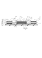
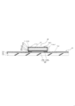
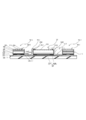
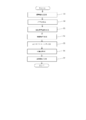
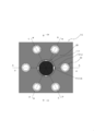
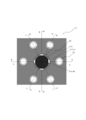
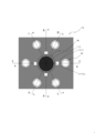
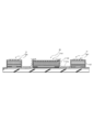
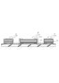
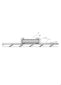
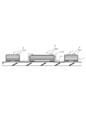
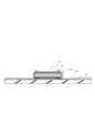
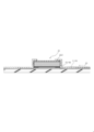
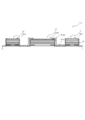
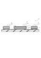
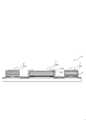
- FIG. 3 is a cross-sectional view taken along the line AA of FIG. It is sectional drawing BB of FIG. It is a cross-sectional view taken along the line CC of FIG. It is a flowchart for demonstrating the manufacturing method of the surface emitting laser apparatus which concerns on Example 1 of one Embodiment of this technique. It is sectional drawing (the 1) for each process of the manufacturing method of the surface light emitting laser apparatus which concerns on Example 1 of one Embodiment of this technique. It is sectional drawing (2) for each process of the manufacturing method of the surface light emitting laser apparatus which concerns on Example 1 of one Embodiment of this technique.
- FIG. 17 is a cross-sectional view taken along the line AA of FIG.
- FIG. 17 is a cross-sectional view taken along the line BB of FIG.
- FIG. 20 is a cross-sectional view taken along the line AA of FIG. 20 is a cross-sectional view taken along the line BB of FIG. It is a top view of the surface emitting laser apparatus which concerns on Example 5 of one Embodiment of this technique.
- FIG. 23 is a cross-sectional view taken along the line AA of FIG. 23.
- FIG. 23 is a cross-sectional view taken along the line BB of FIG. 23.
- FIG. 26 is a cross-sectional view taken along the line AA of FIG. 26.
- FIG. 26 is a cross-sectional view taken along the line BB of FIG. 26. It is a top view of the surface emitting laser apparatus which concerns on Example 7 of one Embodiment of this technique.
- FIG. 29 is a cross-sectional view taken along the line AA of FIG. 29.
- FIG. 29 is a cross-sectional view taken along the line BB of FIG. 29.
- It is a top view of the surface emitting laser apparatus which concerns on Example 8 of one Embodiment of this technique.
- FIG. 32 is a cross-sectional view taken along the line AA of FIG. 32.
- FIG. 32 is a cross-sectional view taken along the line BB of FIG. 32. It is a top view of the surface emitting laser apparatus which concerns on Example 9 of one Embodiment of this technique.
- 35 is a cross-sectional view taken along the line AA of FIG. 35.
- 35 is a cross-sectional view taken along the line BB of FIG. 35.
- It is a top view of the surface emitting laser apparatus which concerns on Example 10 of one Embodiment of this technique.
- FIG. 38 is a cross-sectional view taken along the line AA of FIG. 38.
- FIG. 38 is a cross-sectional view taken along the line BB of FIG. 38. It is sectional drawing of the surface light emitting laser apparatus which concerns on the modification 1 of one Embodiment of this technique. It is sectional drawing of the surface light emitting laser apparatus which concerns on the modification 2 of one Embodiment of this technique.
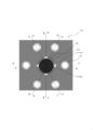
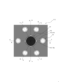
- FIG. 1 is a plan view of the surface emitting laser device 1-1 according to the first embodiment of the present technology.
- FIG. 2 is a cross-sectional view taken along the line AA of FIG.
- FIG. 3 is a cross-sectional view taken along the line BB of FIG.
- FIG. 4 is a cross-sectional view taken along the line CC of FIG.
- the DD line cross section of FIG. 1 is the same as the CC line cross section of FIG.
- the surface emitting laser device according to each embodiment and each modification of the embodiment of the present technology described below is collectively referred to as "surface emitting laser device 1". As shown in FIG.
- the surface emitting laser device 1-1 includes a plurality of (for example, six) light emitting units 10 (10-1 to 10-6) and an electrode unit 20, and a plurality of light emitting units 10 and an electrode unit 20. It is provided with a conductive layer 113-1 that conducts (electrically connects) with. Each light emitting portion 10 and the electrode portion 20 have a mesa structure (see FIGS. 2 to 4).
- the electrode unit 20 is, for example, a common electrode unit common to a plurality of light emitting units 10. Although FIG. 1 shows only one set of a combination of a plurality of light emitting units 10 and an electrode unit 20, the surface emitting laser device 1-1 may have a plurality of sets of this combination.
- the plurality of light emitting units 10 are arranged so as to surround the electrode unit 20 as an example.
- the plurality of light emitting portions 10 and the electrode portion 20 have, for example, a substantially circular outer shape in a plan view.
- each light emitting unit 10 is arranged so that the center is located at different vertices of a regular hexagon centered on the center of the electrode unit 20.
- the surface emitting laser device 1-1 has a laminated structure LS.
- the first contact layer 101, the first multilayer film reflector 102, the first spacer layer 104, the active layer 105, the second spacer layer 106, and the second on the substrate 100 are provided.
- the multilayer film reflector 107, the second contact layer 108, and the electrodes are laminated in this order.
- An oxidative stenosis layer (first or second oxidative stenosis layer 103, 103') is arranged inside the first multilayer film reflector 102.
- the laminated structure LS is formed between the first multilayer film reflecting mirror 102 containing the oxide constriction layer inside, the second multilayer film reflecting mirror 107, and the first and second multilayer film reflecting mirrors 102 and 107. It includes an arranged active layer 105.
- Each light emitting unit 10 constitutes a part of the in-plane direction (direction orthogonal to the stacking direction, the same applies hereinafter) of the laminated structure LS.
- the electrode portion 20 constitutes another portion of the laminated structure LS in the in-plane direction.
- Each light emitting unit 10 has a mesa structure MS1 including a first oxidative constriction layer 103.
- the electrode portion 20 has a mesa structure MS2 including a second oxidative narrowing layer 103'. That is, in the laminated structure LS, the plurality of light emitting portions 10 having the mesa structure MS1 including the first oxide narrowing layer 103 and the electrode portions 20 including the second oxide narrowing layer 103'are located at different positions in the in-plane direction. Have.
- the first and second oxidative constriction layers 103 and 103' are, for example, on substantially the same plane (a plane orthogonal to the stacking direction of the laminated structure LS).
- the light emitting unit 10 includes a first multilayer film reflector 102, a second multilayer film reflector 107, and first and second multilayer film reflectors including a first oxide constriction layer 103 inside. It includes an active layer 105 arranged between 102 and 107.
- the electrode portion 20 includes a first multilayer film reflector 102 containing a second oxide narrowing layer 103', a second multilayer film reflector 107, and first and second multilayer film reflectors 102, 107. Includes an active layer and 105 disposed between.
- the mesa structure MS1 functions as a laser resonator in the light emitting unit 10. That is, the light emitting unit 10 is a surface emitting laser (VCSEL).
- VCSEL surface emitting laser
- Each mesa structure has, for example, a substantially cylindrical shape in a plan view, but may have another pillar shape such as a polygonal pillar shape.
- the center distance between two adjacent two light emitting units 10 among the plurality of light emitting units 10 is preferably 35 ⁇ m or less, and more preferably 20 ⁇ m or less.
- the electrode portion 20 is electrically connected to a laser driver including a driver IC, and a current is supplied from the laser driver.
- the laminated structure LS is covered with the insulating layer 109 except for the region where the electrodes are arranged.
- the insulating layer 109 is made of, for example, SiO 2 , SiN, SiON or the like.
- a contact hole CH1 for drawing out an electrode is formed in the insulating layer 109 covering the top of the mesa structure MS1.
- the cathode electrode 110 is arranged so as to be in contact with the second contact layer 108 of the mesa structure MS1.
- a contact hole CH2 for drawing out an electrode is formed in the insulating layer 109 covering the top of the mesa structure MS2.
- the electrode 112 is arranged so as to be in contact with the second contact layer 108 of the mesa structure MS2.
- the substrate 100 is, for example, a first conductive type GaAs substrate.
- the substrate 100 is arranged on the side opposite to the active layer 105 side with respect to the first multilayer film reflector 102.
- the substrate 100 is transparent with respect to the oscillation wavelength of the light emitting unit 10.
- the first contact layer 101 is made of a first conductive type GaAs-based compound semiconductor.
- the first contact layer 101 is shared by the plurality of light emitting units 10 and the electrode unit 20.
- a contact hole CH3 for drawing out an electrode is formed in the insulating layer 109 that covers the portion between the mesa structure MS1 and the mesa structure MS2 that are adjacent to each other in the laminated structure LS.
- the anode electrode 111 is arranged so as to be in contact with the first contact layer 101.
- the anode electrode 111 is electrically connected to the electrode 112 provided on the top of the mesa structure MS2 via the conductive layer 113-1.
- the conductive layer 113-1 is made of metal plating such as gold plating, silver plating, and copper plating. Details of the conductive layer 113-1 will be described later.
- the anode electrode 111 may have a single-layer structure or a laminated structure.
- the anode electrode 111 is made of at least one metal (including an alloy) selected from the group consisting of, for example, Au, Ag, Pd, Pt, Ni, Ti, V, W, Cr, Al, Cu, Zn, Sn and In. It is composed of.
- the anode electrode 111 has a laminated structure, for example, Ti / Au, Ti / Al, Ti / Al / Au, Ti / Pt / Au, Ni / Au, Ni / Au / Pt, Ni / Pt, Pd / Pt, It is composed of a material such as Ag / Pd.
- the first multilayer film reflector 102 is, for example, a semiconductor multilayer film reflector.
- the multilayer film reflector is also called a distributed Bragg reflector.
- a semiconductor multilayer film reflector which is a kind of multilayer film reflector (distributed Bragg reflector), has low light absorption, high reflectance and conductivity.
- the first multilayer film reflector 102 is also referred to as a lower DBR.
- the first multilayer film reflector 102 is, for example, a first conductive type semiconductor multilayer film reflector, and a plurality of types (for example, two types) of semiconductor layers (refractive index layers) having different refractive indexes from each other have an oscillation wavelength ⁇ . It has a structure in which it is alternately laminated with an optical thickness of 1/4 ( ⁇ / 4) of.
- Each refractive index layer of the first multilayer film reflector 102 is made of, for example, a first conductive type AlGaAs-based compound semiconductor.
- a first oxide narrowing layer 103 is arranged inside the first multilayer film reflector 102 of the light emitting unit 10.
- First oxidized constricting layer 103 has a non-oxidized region 103a formed of AlAs, the oxidized region 103b of oxide of AlAs surrounding the periphery (e.g. Al 2 O 3).
- a second oxidative constriction layer 103' is arranged inside the first multilayer film reflector 102 of the electrode portion 20.
- the second oxidized confinement layer 103 ' as an example, non-oxidized region 103a consisting of AlAs' has a, an oxide of AlAs surrounding the periphery (for example, Al 2 O 3) composed of oxidized region 103b'.
- the first spacer layer 104 is made of a first conductive type AlGaAs-based compound semiconductor.
- the "spacer layer” is also called a "clad layer”.
- the active layer 105 has a quantum well structure including, for example, a barrier layer made of an AlGaAs-based compound semiconductor and a quantum well layer.
- This quantum well structure may be a single quantum well structure (QW structure) or a multiple quantum well structure (MQW structure).
- the second spacer layer 106 (upper spacer layer) is made of a second conductive type AlGaAs-based compound semiconductor.
- the "spacer layer” is also called a "clad layer”.
- the second multilayer film reflector 107 is, for example, a second conductive type semiconductor multilayer film reflector, in which a plurality of types (for example, two types) of semiconductor layers (refractive index layers) having different refractive indexes have different oscillation wavelengths. It has a structure in which layers are alternately laminated with an optical thickness of 1/4 wavelength.
- Each refractive index layer of the second multilayer film reflector 107 is made of, for example, a second conductive type AlGaAs-based compound semiconductor.
- the second contact layer 108 is made of, for example, a second conductive type GaAs-based compound semiconductor.
- the cathode electrode 110 may have a single-layer structure or a laminated structure.
- the cathode electrode 110 is made of at least one metal (including an alloy) selected from the group consisting of, for example, Au, Ag, Pd, Pt, Ni, Ti, V, W, Cr, Al, Cu, Zn, Sn and In. It is composed of.
- the cathode electrode 110 has a laminated structure, for example, Ti / Au, Ti / Al, Ti / Al / Au, Ti / Pt / Au, Ni / Au, Ni / Au / Pt, Ni / Pt, Pd / Pt, It is composed of a material such as Ag / Pd.
- the electrode 112 may have a single-layer structure or a laminated structure.
- the electrode 112 is made of, for example, by at least one metal (including an alloy) selected from the group consisting of Au, Ag, Pd, Pt, Ni, Ti, V, W, Cr, Al, Cu, Zn, Sn and In. It is configured.
- the electrode 112 has a laminated structure, for example, Ti / Au, Ti / Al, Ti / Al / Au, Ti / Pt / Au, Ni / Au, Ni / Au / Pt, Ni / Pt, Pd / Pt, Ag. It is composed of materials such as / Pd.
- the conductive layer 113-1 conducts each of the plurality of (for example, six) light emitting portions 10-1 with the electrode portion 20.
- the conductive layer 113-1 is a region between each of the plurality of light emitting portions 10-1 and the electrode portion 20 of the laminated structure LS and an outer peripheral surface of the electrode portion 20 as shown in FIGS. 2 to 4. And covers the outer periphery of the upper surface. More specifically, the conductive layer 113-1 is formed from the first portion P1 of the laminated structure LS that covers the region between each light emitting portion 10 and the electrode portion 20, and the light emitting portion 10 relative to the electrode portion 20.
- the first to third portions P1 to P3 are a series of integral parts.
- the first portion P1 covering the region between the light emitting portion 10-1 and the electrode portion 20 of the conductive layer 113-1 is the first portion P1-1.
- the second portion P2 of the conductive layer 113-1 covering the near half portion NH1 relatively close to the light emitting portion 10-1 of the electrode portion 20 is the second portion P2-1. be.
- the third portion P3 of the conductive layer 113-1 covering the far half portion FH1 relatively far from the light emitting portion 10-1 of the electrode portion 20 is the third portion P3-1. be.
- the first portion P1 covering the region between the light emitting portion 10-2 and the electrode portion 20 of the conductive layer 113-1 is the first portion P1-2.
- the second portion P2 of the conductive layer 113-1 covering the near half portion NH2 relatively close to the light emitting portion 10-2 of the electrode portion 20 is the second portion P2-2. be.
- the third portion P3 of the conductive layer 113-1 covering the far half portion FH2 of the electrode portion 20 relatively far from the light emitting portion 10-2 is the third portion P3-2. be.
- the conductive layer 113-1 is provided with a degassing portion 113-1a in the first portion P1 and / or the second portion P2 corresponding to each light emitting portion 10 and the third portion P3.
- the degassing portion 113-1a is, for example, a notch portion.
- four degassing portions 113-1a are provided at equal intervals in the circumferential direction of the electrode portion 20.
- the degassing portion 113-1a is provided at a position within 35 ⁇ m from the oxidation region 103b'of the second oxide constriction layer 103'of the conductive layer 113-1, and at a position within 30 ⁇ m. It is more preferably provided, even more preferably it is provided at a position within 25 ⁇ m, and even more preferably it is provided at a position within 20 ⁇ m.
- the light emitting unit 10 is typically used. -1, Only the explanation related to the light emitting unit 10-2 will be given.
- the degassing section 113-1a provided in the second portion P2-1 corresponding to the light emitting section 10-1 is the degassing section 113-1a-1.
- the degassing section 113-1a provided in the third portion P3-1 corresponding to the light emitting section 10-1 is the degassing section 113-1a-3.
- the degassing portion 113-1a provided straddling the second portion P2-1 and the third portion P3-1 corresponding to the light emitting portion 10-1 is the degassing portion 113-1a-. 2 and the degassing portion 113-1a-4.
- the degassing portion 113-1a-1 is provided at least on the portion of the second portion P2-1 that covers the side surface of the near half portion NH1.
- the degassing portion 113-1a-3 is provided at least at a portion of the third portion P3-1 that covers the side surface of the far half portion FH1.
- the degassing portion 113-1a-2 is composed of at least a portion of the second portion P2-1 covering the side surface of the near half portion NH1 and a portion of the third portion P3-1. It is provided so as to straddle the portion covering the side surface of the far half portion FH1.
- the degassing portion 113-1a-4 includes at least a portion of the second portion P2-1 covering the side surface of the near half portion NH1 and a portion of the third portion P3-1 covering the side surface of the far half portion FH1. It is provided across the area.
- the degassing portion 113-1a-1 is the outer periphery of the second oxidative constriction layer 103'of the portion of the second portion P2-1 that covers the side surface of the near half portion NH1. It is provided at least at a position corresponding to the surface (the outer peripheral surface of the oxidation region 103b').
- the degassing portion 113-1a-3 is an outer peripheral surface of the second oxide narrowing layer 103'(the outer peripheral surface of the oxidation region 103b') of the portion of the third portion P3-1 that covers the side surface of the far half portion FH1. It is provided at least in the position corresponding to. As shown in FIGS.
- the degassing portion 113-1a-2 is at least the second oxidative stenosis layer 103'of the portion of the second portion P2-1 that covers the side surface of the near half NH1.
- the degassing portion 113-1a-4 is at least the outer peripheral surface of the second oxide narrowing layer 103'(the outer periphery of the oxidation region 103b', which is a portion of the second portion P2-1 covering the side surface of the near half portion NH1. Corresponds to the position corresponding to the surface) and the outer peripheral surface of the second oxide narrowing layer 103'(the outer peripheral surface of the oxidation region 103b') of the portion of the third portion P3-1 that covers the side surface of the far half FH1. It is provided so as to straddle the position where it is to be used.
- the degassing portion 113-1a-1 is provided at least in a portion of the second portion P2-1 that covers the upper surface of the near half portion NH1. More specifically, the degassing portion 113-1a-1 is provided at least at a portion of the second portion P2-1 that covers the outer peripheral portion of the upper surface of the near half portion NH1.
- the degassing portion 113-1a-3 is provided at least at a portion of the third portion P3-1 that covers the upper surface of the far half portion FH1. More specifically, the degassing portion 113-1a-3 is provided at least at a portion of the third portion P3-1 that covers the outer peripheral portion of the upper surface of the far half portion FH. As shown in FIGS.
- the degassing portion 113-1a-2 has at least the upper surface (more specifically, the outer peripheral portion of the upper surface) of the near half portion NH1 of the second portion P2-1. It is provided so as to straddle the portion to be covered and the portion of the third portion P3-1 that covers the upper surface of the far half portion FH1 (more specifically, the outer peripheral portion of the upper surface).
- the degassing portion 113-1a-4 includes at least a portion of the second portion P2-1 covering the upper surface of the near half portion NH1 and a portion of the third portion P3-1 covering the upper surface of the far half portion FH1. It is provided across the area.
- the degassing portion 113-1a-1 is provided at least at a portion of the second portion P2-1 that covers the corner portion formed by the upper surface and the side surface of the near half portion NH1.
- the degassing portion 113-1a-3 is provided at least at a portion of the third portion P3-1 that covers the corner portion formed by the upper surface and the side surface of the far half portion FH1.
- the degassing portion 113-1a-2 is at least a portion of the second portion P2-1 covering the corner portion formed by the upper surface and the side surface of the near half portion NH1.
- the third portion P3-1 is provided so as to straddle the portion covering the corner portion formed by the upper surface and the side surface of the far half portion FH1.
- the degassing portion 113-1a-4 is at least a far half of the second portion P2-1, a portion covering the corner formed by the upper surface and the side surface of the near half portion NH1 and the third portion P3-1. It is provided so as to straddle the portion covering the corner portion formed by the upper surface and the side surface of the portion FH1.
- the degassing portion 113-1a-1 is provided at least at the boundary portion between the first portion P1-1 and the second portion P2-1.
- An insulating layer 109 is arranged between the 20 and the far half FH1.
- insulators have a lower gas barrier property than metals and semiconductors. That is, the insulating layer 109 has a lower gas barrier property than the semiconductor layers of the conductive layer 113-1 and the electrode portion 20.
- the thickness of the insulating layer 109 is preferably 0.1 ⁇ m or more and 2.0 ⁇ m or less.
- the degassing section 113-1a provided in the second portion P2-2 corresponding to the light emitting section 10-2 is the degassing section 113-1a-1 and the degassing section 113-1a-2. be.
- the degassing section 113-1a provided in the third portion P3-2 corresponding to the light emitting section 10-2 is the degassing section 113-1a-3 and the degassing section 113-1a-4. be.
- the degassing portion 113-1a-1 is provided at least on the portion of the second portion P2-2 that covers the side surface of the near half portion NH2.
- the degassing portion 113-1a-2 is provided at least at a portion of the second portion P2-2 that covers the side surface of the near half portion NH2.
- the degassing portion 113-1a-3 is provided at least at a portion of the third portion P3-2 that covers the side surface of the far half portion FH2.
- the degassing portion 113-1a-4 is provided at least at a portion of the third portion P3-2 that covers the side surface of the far half portion FH2.
- the degassing portion 113-1a-1 is provided at least at a portion of the second portion P2-2 that covers the upper surface of the near half portion NH2. More specifically, the degassing portion 113-1a-1 is provided at least at a portion of the second portion P2-2 that covers the outer peripheral portion of the upper surface of the near half portion NH2. The degassing portion 113-1a-2 is provided at least at a portion of the second portion P2-2 that covers the upper surface of the near half portion NH2. More specifically, the degassing portion 113-1a-2 is provided at least at a portion of the second portion P2-2 that covers the outer peripheral portion of the upper surface of the near half portion NH2.
- the degassing portion 113-1a-3 is provided at least at a portion of the third portion P3-2 that covers the upper surface of the far half portion FH2. More specifically, the degassing portion 113-1a-3 is provided at least at a portion of the third portion P3-2 that covers the outer peripheral portion of the upper surface of the far half portion FH2.
- the degassing portion 113-1a-4 is provided at least at a portion of the third portion P3-2 that covers the upper surface of the far half portion FH2. More specifically, the degassing portion 113-1a-4 is provided at least at a portion of the third portion P3-2 that covers the outer peripheral portion of the upper surface of the far half portion FH2.
- the degassing portion 113-1a-1 is provided at least at a portion of the second portion P2-2 that covers the corner portion formed by the upper surface and the side surface of the near half portion NH2.
- the degassing portion 113-1a-2 is provided at least at a portion of the second portion P2-2 that covers the corner portion formed by the upper surface and the side surface of the near half portion NH2.
- the degassing portion 113-1a-3 is provided at least at a portion of the third portion P3-2 that covers the corner portion formed by the upper surface and the side surface of the far half portion FH2.
- the degassing portion 113-1a-4 is provided at least at a portion of the third portion P3-2 that covers the corner portion formed by the upper surface and the side surface of the far half portion FH2.
- An insulating layer 109 is arranged between the 20 and the far half FH2.
- the insulating layer 109 has a lower gas barrier property than the semiconductor layers of the conductive layer 113-1 and the electrode portion 20.
- the thickness of the insulating layer 109 is preferably 0.1 ⁇ m or more and 2.0 ⁇ m or less.
- the current injected from the laser driver into the anode electrode 111 via the electrode unit 20 is supplied to the light emitting unit 10 to be emitted via the first contact layer 101.
- the current supplied to the light emitting unit 10 is injected into the active layer 105 via the first multilayer film reflector 102, the first oxidation narrowing layer 103, and the first spacer layer 104 of the light emitting unit 10.
- the active layer 105 emits light and the light is amplified while being repeatedly reflected between the first and second multilayer film reflecting mirrors 102 and 107 to satisfy the oscillation conditions, the laser is directed to the back surface side of the substrate 100. It is emitted as light.
- the laminated body L is generated. Specifically, using a chemical vapor deposition (CVD) method, for example, an organometallic vapor deposition (MOCVD) method, a first contact layer 101 and a first contact layer 101 on the substrate 100, as shown in FIG.
- CVD chemical vapor deposition
- MOCVD organometallic vapor deposition
- the contact layers 108 are laminated in this order to form a laminated body L.
- a mesa is formed. Specifically, as shown in FIG. 7, the laminated body L is etched to form mesas M1 and M2. More specifically, first, a resist pattern for forming mesas M1 and M2 to be mesas structures MS1 and MS2 is generated on the second contact layer 108 of the laminated body L. Next, the laminate L is etched (for example, wet etching using a sulfuric acid-based etchant) using this resist pattern as a mask to form mesas M1 and M2. Here, etching is performed until the first contact layer 101 is exposed. After that, the resist pattern is removed.
- an oxidative stenosis layer is formed.
- the peripheral portion of the selected oxide layer 103S of the mesas M1 and M2 is oxidized to form the first and second oxide narrowing layers 103 and 103'.
- the first and second medas M1 and M2 are exposed to a water vapor atmosphere, the selected oxide layer 103S is oxidized (selectively oxidized) from the side surface, and the non-oxidized region is surrounded by the oxidized region. Oxidized narrowing layers 103, 103'are formed.
- gas is intermittently or continuously generated from the oxidation region of each oxidation constriction layer due to the heat during selective oxidation.
- the insulating layer 109 is formed. Specifically, as shown in FIG. 9, the insulating layer 109 is formed on the laminate on which the mesas M1 and M2 are formed.
- a contact hole is formed. Specifically, a resist pattern for forming the cathode electrode 110, the electrode 112, and the anode electrode 111 is generated on the laminate on which the mesas M1 and M2 are formed and the insulating layer 109 is formed. Next, using this resist pattern as a mask, the insulating layer 109 at the location where the cathode electrode 110, the electrode 112, and the anode electrode 111 will be provided is removed by etching (for example, etching using a hydrofluoric acid-based etchant) to remove the contact hole. It forms CH1, CH2, and CH3 (see FIG. 10).
- the electrodes are formed. Specifically, for example, an Au / Ti film is formed on the laminate on which the contact holes CH1, CH2, and CH3 are formed by an EB vapor deposition method, and the resist and the resist, for example Au / Ti, are lifted off. As a result, the cathode electrode 110, the electrode 112, and the anode electrode 111 are formed (see FIG. 11).
- the conductive layer is formed. Specifically, first, for example, a metal film MF (for example, gold plating) is formed into a film by using a plating method (see FIG. 12). Before using the plating method, a base layer (for example, nickel) to be a seed for plating is used, for example, by vapor deposition, sputtering, or the like on a portion of the insulating layer 109 where the conductive layer 113-1 is to be formed. Plating, chrome plating, etc.) are formed. The thickness of the metal film MF is a thickness (for example, about 2 ⁇ m) that can sufficiently prevent a voltage drop.
- a metal film MF for example, gold plating
- a resist pattern for removing the portion covering each electrode and the portion where the degassing portion 113-1a is to be formed is formed on the metal film MF.
- the metal film MF is etched (for example, wet etching using a sulfuric acid-based etchant) using the resist pattern as a mask to form the conductive layer 113-1 having the degassing portion 113-1a (see FIG. 13). ).
- the conductive layer 113-1 may be formed by lift-off instead of etching.
- processing such as annealing, thinning by polishing the back surface of the wafer, and non-reflective coating on the back surface of the wafer is performed, and a plurality of surface emitting laser devices 1-1 are formed on one wafer. After that, a plurality of surface emitting laser devices 1-1 are separated for each device (each chip) by dicing.
- the plurality of light emitting portions 10 including the first oxide narrowing layer 103 and the electrode portion 20 including the second oxide narrowing layer 103' are different in the in-plane direction.
- a laminated structure LS held at a position and a conductive layer 113-1 for conducting each light emitting portion 20 and an electrode portion 20 are provided.
- the conductive layer 113-1 is a first portion P1 of the laminated structure LS that covers the region between each light emitting portion 10 and the electrode portion 20, and a near half portion of the electrode portion 20 that is relatively close to the light emitting portion 10.
- a degassing portion 113-1a is provided in the first portion P1 and / or the second portion P2 and the third portion P3.
- the gas generated in the oxidized region of the second oxidized narrowing layer 103' is the degassing portion 113- provided in the first portion P1 and / or the second portion P2 and the third portion P3. It is released to the outside via 1a.
- defects such as gas swelling of the conductive layer 113-1 can be suppressed.
- defects such as gas swelling of the electrode 112 provided at the top of the electrode portion 20 can be suppressed.
- the surface emitting laser device 1-1 it is possible to provide a surface emitting laser device capable of improving the yield.
- gas may be generated in the second oxide narrowing layer 103'due to heat generated during operation, environmental temperature, etc. even after manufacturing, so that the degassing portion 113-1a is used.
- the device it is possible to improve the reliability of the surface emitting laser device 1-1 after it is made into a product.
- the degassing portion is provided. Gas cannot be discharged to the outside from the portion (the former and / or the latter) where is not provided, and defects such as gas swelling occur in the portion and the electrode provided at the top of the electrode portion. Therefore, the yield cannot be improved and the reliability as a product is inferior.
- the degassing portion 113-1a is a notch portion. As a result, the degassing portion 113-1a can be easily formed on the conductive layer 113-1. Specifically, the degassing portion 113-1a can be formed at the time of patterning of the conductive layer 113-1.
- the surface emitting laser apparatus 1-1 between the first portion P1 and the laminated structure LS, between the second portion P2 and the near half portion NH, and between the third portion P3 and the far half. Further, an insulating layer 109 is provided between the parts and the FH. As a result, the gas generated in the oxidized region of the second oxide narrowing layer 103'can be quickly guided to the degassing portion 113-1a via the insulating layer 109 having a low gas barrier property, and degassing. Efficiency can be increased.
- the passage of the gas to the inside of the insulating layer 109 is improved.
- the thinner the insulating layer 109 the more gas generated in the second oxide narrowing layer 103', passing through (penetrating) the insulating layer 109 in the thickness direction, and reaching the degassing portion 113-1a.
- the penetration of the insulating layer 109 is improved.
- the thickness of the insulating layer 109 is set to 0.1 ⁇ m or more and 2.0 ⁇ m or less.
- the degassing portion 113-1a is provided at least in a portion of the second portion P2 that covers the side surface of the near half portion NH and a portion of the third portion P3 that covers the side surface of the far half portion FH. As a result, at least a part of the gas generated in the second oxidative constriction layer 103'can be sent to the degassing portion 113-1a by a relatively short route.
- the degassing portion 113-1a is a second oxidative stenosis layer 103 of a portion of the second portion P2 covering the side surface of the near half portion NH and a portion of the third portion P3 covering the side surface of the far half portion FH. It is provided at a position corresponding to the outer peripheral surface of'. As a result, at least a part of the gas generated in the second oxidative constriction layer 103'can be sent to the degassing portion 113-1a by the shortest path.
- the degassing portion 113-1a is provided at least in a portion of the second portion P2 that covers the upper surface of the near half portion NH and a portion of the third portion that covers the upper surface of the far half portion FH. As a result, at least a part of the gas generated in the second oxidative constriction layer 103'can be sent to the degassing portion 113-1a by a relatively short route.
- the degassing portion 113-1a is provided at least in a portion of the second portion P2 that covers the outer peripheral portion of the upper surface of the near half portion NH and a portion of the third portion P3 that covers the outer peripheral portion of the upper surface of the far half portion FH. ing. As a result, at least a part of the gas generated in the second oxidative constriction layer 103'can be sent to the degassing portion 113-1a by a shorter route.
- the degassing portion 113-1a is a portion of the second portion P2 that covers the corner formed by the upper surface and the side surface of the near half portion NH, and the upper surface and the side surface of the far half portion FH of the third portion P3. It is provided at least in the portion covering the formed corner. As a result, at least a part of the gas generated in the second oxidative constriction layer 103'can be sent to the degassing portion 113-1a by a relatively short route.
- the degassing portion 113-1a is provided at least at the boundary between the first portion P1 and the second portion P2. At least a part of the gas generated in the second oxidative constriction layer 103'can be sent to the degassing portion 113-1a by a relatively short route.
- the degassing portion 113-1a is provided at a position within 35 ⁇ m from the oxidation region of the second oxide constriction layer 103'of the conductive layer 113-1.
- the distance from the second oxidative constriction layer 103', which is the source of the gas, to the degassing portion 113-1a can be set to a distance at which the gas can be released quickly and reliably.
- the conductive layer 113-1 conducts each of the plurality of light emitting portions 10 with the electrode portion 20. As a result, the number of electrode portions 20 can be reduced, and the configuration can be simplified.
- the conductive layer 113-1 covers the region between each of the plurality of light emitting portions 10 and the electrode portion 20 of the laminated structure LS, and the outer peripheral surface and the outer peripheral portion of the upper surface of the electrode portion 20. As a result, the current can be efficiently supplied from the electrode unit 20 to each light emitting unit 10.
- the center distance between two adjacent two light emitting units 10 among the plurality of light emitting units 10 is preferably 35 ⁇ m or less.
- the gas pressure of the gas generated in the second oxide narrowing layer 103' is likely to increase. Therefore, it is particularly effective to provide the degassing portion 113-1a on the conductive layer 113-1.
- the current density of the electrode portion 20 becomes high and the gas pressure tends to rise. Therefore, it is particularly effective to provide the degassing portion 113-1a in the conductive layer 113-1.
- the light emitting unit 20 includes a first multilayer film reflector 102 containing a first oxide constriction layer 103 inside, a second multilayer film reflector 107, and first and second multilayer film reflectors 102 and 107.
- the electrode portion 20 includes the active layer 105 arranged between the first multilayer mirror 102 and the second multilayer reflector 107 containing the second oxide constriction layer 103'inside the electrode portion 20. Includes an active layer 105 disposed between the first and second multilayer reflectors 102, 107. Thereby, the light emitting portion 10 and the electrode portion 20 can be formed in parallel by the semiconductor manufacturing process.
- the light emitting unit 20 is arranged on the side opposite to the active layer 105 side with respect to the first multilayer film reflector 102, and includes a substrate 100 that is transparent to the oscillation wavelength of the light emitting unit 20, and the light emitting unit 20 is a substrate. Light is emitted to the back surface side of 100. This makes it possible to realize a thin and low power consumption surface emitting laser device 1-1.
- the method for manufacturing the surface emitting laser apparatus 1-1 according to the first embodiment is a first multilayer film reflecting mirror 102, an active layer 105, and a second multilayer film reflecting mirror containing the selected oxide layer 103S on the substrate 100.
- Conductive layer 113-having a second portion P2 covering the near half portion NH close to the light emitting portion 10 and a third portion P3 covering the far half portion FH relatively far from the light emitting portion 10 of the electrode portion 20. Includes a step of forming 1.
- the degassing portion 113-1a is formed in the first portion P1 and / or the second portion P2 and the third portion P3.
- the gas generated in the oxidized region of the second oxidized narrowing layer 103' is the degassing portion 113- provided in the first portion P1 and / or the second portion P2 and the third portion P3. It is released to the outside via 1a.
- the surface emitting laser device 1-1 capable of improving the yield can be manufactured.
- the degassing portion 113-1a is a notch portion. As a result, the degassing portion 113-1a can be easily formed on the conductive layer 113-1. The degassing portion 113-1a can be formed during patterning of the conductive layer 113-1.
- the light emitting portion 10 of the laminated structure LS is used. Further, the step of forming the insulating layer 109 in the region between the electrode portion 20 and the near half portion NH and the far half portion FH is included. As a result, the surface emitting laser device 1-1 having high degassing efficiency can be manufactured.
- FIG. 14 is a plan view of the surface emitting laser device 1-2.
- FIG. 15 is a cross-sectional view taken along the line AA of FIG.
- FIG. 16 is a cross-sectional view taken along the line BB of FIG.
- the CC line cross section and the DD line cross section of FIG. 14 are the same as the CC line cross section of FIG.
- the degassing portion 113-2a is a second portion P2 of the conductive layer 113-2 that covers the near half portion NH of the electrode portion 20.
- each degassing portion 113-2a is formed by the upper surface and the side surface of the second portion P2 of the conductive layer 113-2 that covers the near half portion NH of the electrode portion 20.
- FIG. 17 is a plan view of the surface emitting laser device 1-3.
- FIG. 18 is a cross-sectional view taken along the line AA of FIG.
- FIG. 19 is a cross-sectional view taken along the line BB of FIG.
- the CC line cross section and the DD line cross section of FIG. 17 are the same as the CC line cross section of FIG.
- each degassing portion 113-3a is a second portion P2 of the conductive layer 113-3 that covers the near half portion NH of the electrode portion 20.
- FIG. 20 is a plan view of the surface emitting laser device 1-4.
- 21 is a cross-sectional view taken along the line AA of FIG. 20.
- FIG. 22 is a cross-sectional view taken along the line BB of FIG.
- the CC line cross section and the DD line cross section of FIG. 20 are the same as the CC line cross section of FIG.
- each degassing portion 113-4a is located between the light emitting portion 10 and the electrode portion 20 in the laminated structure LS of the conductive layer 113-4.
- Each degassing portion 113-4a is a second oxidative constriction layer in a portion of the conductive layer 113-4 that covers the side surface of the near half portion NH of the second portion P2 that covers the near half portion NH of the electrode portion 20.
- Second oxidative stenosis at the position corresponding to the outer peripheral surface of 103'and at the portion of the conductive layer 113-4 that covers the far half FH of the electrode portion 20 and the third portion P3 that covers the side surface of the far half FH. It is provided at least at a position corresponding to the outer peripheral surface of the layer 103'.
- FIG. 23 is a plan view of the surface emitting laser device 1-5.
- FIG. 24 is a cross-sectional view taken along the line AA of FIG. 23.
- FIG. 25 is a cross-sectional view taken along the line BB of FIG. 23.
- the CC line cross section and the DD line cross section of FIG. 23 are the same as the CC line cross section of FIG.
- each degassing portion 113-5a is located between the light emitting portion 10 and the electrode portion 20 of the laminated structure LS of the conductive layer 113-5. It is an opening provided in the first portion P1 that covers the region.
- FIG. 26 is a plan view of the surface emitting laser device 1-6.
- 27 is a cross-sectional view taken along the line AA of FIG. 26.
- FIG. 28 is a cross-sectional view taken along the line BB of FIG. 26.
- the CC line cross section and the DD line cross section of FIG. 26 are the same as the CC line cross section of FIG.
- each degassing portion 113-6a is located between the light emitting portion 10 and the electrode portion 20 in the laminated structure LS of the conductive layer 113-6.
- a notch or opening provided in the first portion P1 covering the area.
- FIG. 29 is a plan view of the surface emitting laser device 1-7.
- FIG. 30 is a cross-sectional view taken along the line AA of FIG. 29.
- FIG. 31 is a cross-sectional view taken along the line BB of FIG. 29.
- the CC line cross section and the DD line cross section of FIG. 29 are the same as the CC line cross section of FIG.
- each degassing portion 113-7a is a second portion P2 of the conductive layer 113-7 that covers the near half portion NH of the electrode portion 20.
- FIG. 32 is a plan view of the surface emitting laser device 1-8.
- 33 is a cross-sectional view taken along the line AA of FIG. 32.
- FIG. 34 is a cross-sectional view taken along the line BB of FIG. 32.
- the CC line cross section and the DD line cross section of FIG. 32 are the same as the CC line cross section of FIG.
- each degassing portion 113-8a is a second portion P2 of the conductive layer 113-8 that covers the near half portion NH of the electrode portion 20.
- Each degassing portion 113-8a forms a corner portion of the conductive layer 113-8 formed by the upper surface and the side surface of the second portion P2 covering the near half portion NH of the electrode portion 20.
- Each degassing portion 113-8a includes a portion of the conductive layer 113-8 that covers the side surface of the near half portion NH of the second portion P2 that covers the near half portion NH of the electrode portion 20 and a portion of the conductive layer 113-8 that covers the side surface of the near half portion NH.
- the third portion P3 that covers the far half FH of the electrode portion 20 is provided at least at a portion that covers the side surface of the far half FH.
- Each degassing portion 113-8a is a boundary portion between the first portion P1 and the second portion P2 of the conductive layer 113-8, which covers the region between the light emitting portion 10 and the electrode portion 20 in the laminated structure LS. It is provided at least near the bottom of the mesa structure MS2).
- Each degassing portion 113-8a is a second oxidative constriction layer in a portion of the conductive layer 113-8 that covers the side surface of the near half portion NH of the second portion P2 of the electrode portion 20. Second oxidative stenosis at the position corresponding to the outer peripheral surface of 103'and at the portion of the conductive layer 113-4 that covers the far half FH of the electrode portion 20 and the third portion P3 that covers the side surface of the far half FH. It is provided at least at a position corresponding to the outer peripheral surface of the layer 103'.
- Each degassing portion 113-8a is an opening.
- FIG. 35 is a plan view of the surface emitting laser device 1-9.
- FIG. 36 is a cross-sectional view taken along the line AA of FIG. 35.
- FIG. 37 is a cross-sectional view taken along the line BB of FIG. 35.
- the CC line cross section and the DD line cross section of FIG. 35 are the same as the CC line cross section of FIG. As shown in FIGS.
- each degassing portion 113-9a is a second portion P2 of the conductive layer 113-9 that covers the near half portion NH of the electrode portion 20.
- FIG. 38 is a plan view of the surface emitting laser device 1-10.
- FIG. 39 is a cross-sectional view taken along the line AA of FIG. 38.
- FIG. 40 is a cross-sectional view taken along the line BB of FIG. 38.
- the CC line cross section and the DD line cross section of FIG. 38 are the same as the CC line cross section of FIG. As shown in FIGS.
- each degassing portion 113-10a is located between the light emitting portion 10 and the electrode portion 20 in the laminated structure LS of the conductive layer 113-10. It is an opening provided at the boundary between the first portion P1 and the second portion P2 covering the region (near the bottom of the mesa structure MS2).
- Each degassing portion 113-10a is a second oxidative constriction layer in a portion of the conductive layer 113-10 that covers the side surface of the near half portion NH of the second portion P2 of the electrode portion 20.
- a second oxidative stenosis at a position corresponding to the outer peripheral surface of 103'and at a portion of the conductive layer 113-10 that covers the far half FH of the electrode portion 20 and the third portion P3 that covers the side surface of the far half FH. It is provided at least at a position corresponding to the outer peripheral surface of the layer 103'.
- the surface emitting laser devices 1-11 to 1-120 according to the modified examples 1 to 10 of the embodiment of the present technology will be described.
- the surface emitting laser devices 1-11 to 1-20 according to the modified examples 1 to 10 are different from the surface emitting laser devices according to the above embodiments in that the degassing portion is a thin film portion.
- the surface emitting laser devices 1-2 to 1-10 according to the second to tenth examples can be manufactured by the same manufacturing method as the manufacturing method of the surface emitting laser device 1-1 according to the first embodiment.
- a base layer for example, nickel plating, chrome plating, etc.
- a thin film portion which is a degassing portion is provided using the resist pattern.
- a metal film for example, metal plating
- the thin film portion composed of only the base layer has a significantly lower gas barrier property than the portion in which the plating layer is laminated on the base layer.
- the surface emitting laser device according to each modification has a configuration substantially similar to that in FIG. 1 in a plan view.
- 41 to 50 are cross-sectional views of the surface emitting laser apparatus according to each modification (corresponding to the cross-sectional view taken along the line AA of FIG. 1).
- the other cross sections of the surface emitting laser device according to each modification are substantially the same as the BB line cross section, the CC line cross section, and the DD line cross section of FIG.
- the position of the degassing portion 113-11a provided in the conductive layer 113-11 is set to the first embodiment shown in FIGS. 1 to 4. It corresponds to the position of the degassing portion 113-1a in the surface emitting laser device 1-1.
- the degassing portion 113-11a is a thin film portion composed of only the base layer of the conductive layer 113-11.
- the position of the degassing portion 113-12a provided in the conductive layer 113-12 is set to the second embodiment shown in FIGS. 14 to 16. It corresponds to the position of the degassing portion 113-2a in the surface emitting laser device 1-2.
- the degassing portion 113-12a is a thin film portion composed of only the base layer of the conductive layer 113-12.
- the position of the degassing portion 113-13a provided in the conductive layer 113-13 is set to the third embodiment shown in FIGS. 17 to 19. It corresponds to the position of the degassing portion 113-3a in the surface emitting laser device 1-3.
- the degassing portion 113-13a is a thin film portion composed of only the base layer of the conductive layer 113-13.
- the position of the degassing portion 113-14a provided in the conductive layer 113-14 is set to the fourth embodiment shown in FIGS. 20 to 22. It corresponds to the position of the degassing portion 113-4a in the surface emitting laser device 1-4.
- the degassing portion 113-14a is a thin film portion composed of only the base layer of the conductive layer 113-14.
- the position of the degassing portion 113-15a provided in the conductive layer 113-15 is set to the fifth embodiment shown in FIGS. 23 to 25. It corresponds to the position of the degassing portion 113-5a in the surface emitting laser device 1-5.
- the degassing portion 113-15a is a thin film portion composed of only the base layer of the conductive layer 113-15.
- the position of the degassing portion 113-16a provided in the conductive layer 113-16 is set to the sixth embodiment shown in FIGS. 26 to 28. It corresponds to the position of the degassing portion 113-6a in the surface emitting laser device 1-6.
- the degassing portion 113-16a is a thin film portion composed of only the base layer of the conductive layer 113-16.
- the position of the degassing portion 113-17a provided in the conductive layer 113-17 is set to the seventh embodiment shown in FIGS. 29 to 31. It corresponds to the position of the degassing portion 113-7a in the surface emitting laser device 1-7.
- the degassing portion 113-17a is a thin film portion composed of only the base layer of the conductive layer 113-17.
- the position of the degassing portion 113-18a provided in the conductive layer 113-18 is set to the eighth embodiment shown in FIGS. 32 to 34. It corresponds to the position of the degassing portion 113-8a in the surface emitting laser device 1-8.
- the degassing portion 113-18a is a thin film portion composed of only the base layer of the conductive layer 113-18.
- the position of the degassing portion 113-19a provided in the conductive layer 113-19 is set to the ninth embodiment shown in FIGS. 35 to 37. It corresponds to the position of the degassing portion 113-9a in the surface emitting laser device 1-9.
- the degassing portion 113-19a is a thin film portion composed of only the base layer of the conductive layer 113-19.
- the position of the degassing portion 113-20a provided in the conductive layer 113-20 is set to the tenth embodiment shown in FIGS. 38 to 40. It corresponds to the position of the degassing portion 113-10a in the surface emitting laser device 1-10.
- the degassing portion 113-20a is a thin film portion composed of only the base layer of the conductive layer 113-20.
- the number of the light emitting unit 10 and the electrode unit 20 of the surface emitting laser device 1 according to the embodiment of the present technology can be appropriately changed.
- the surface emitting laser device 1 according to the present technology may have at least one set of a single light emitting unit 10 and a single electrode unit 20.
- the number of degassing portions of the surface emitting laser device 1 according to the embodiment of the present technology is not limited to four for one electrode portion 20, but may be one to three or five. It may be the above.
- the arrangement of the degassing portion of the surface emitting laser device 1 according to the embodiment of the present technology can be appropriately changed according to the shape of the conductive layer and / or the electrode portion.
- the plurality of degassing portions do not necessarily have to be arranged at equal intervals.
- the insulating layer 109 is provided between the first portion P1 and the laminated structure LS, between the second portion P2 and the near half portion NH, and between the third portion P3 and the far half portion FH. It may be arranged.
- the second portion is provided.
- the thickness of the insulating layer 109 may be made as thin as possible (for example, as close as possible to 0.1 ⁇ m) between the portion P2 and the near half portion NH.
- the third portion is provided.
- the thickness of the insulating layer 109 may be made as thin as possible (for example, as close as possible to 0.1 ⁇ m) between the portion P3 and the far half FH.
- the thickness of the insulating layer may be less than 0.1 ⁇ m or thicker than 2.0 ⁇ m.
- the degassing portion may be provided at least in a portion of the second portion P2 that covers the side surface of the near half portion NH or a portion of the third portion P3 that covers the side surface of the far half portion FH.
- the degassing portion is the portion of the second portion P2 that covers the side surface of the near half NH or the portion of the third portion that covers the side surface of the far half FH of the second oxidative stenosis layer 103'. It may be provided at a position corresponding to the outer peripheral surface.
- the degassing portion may be provided at least in a portion of the second portion P2 that covers the upper surface of the near half portion NH or a portion of the third portion P3 that covers the upper surface of the far half portion FH.
- the degassing portion is provided at least in a portion of the second portion P2 that covers the outer peripheral portion of the upper surface of the near half portion NH or a portion of the third portion P3 that covers the outer peripheral portion of the upper surface of the far half portion FH. May be.
- the degassing portion is formed by a portion of the second portion P2 that covers the corner formed by the upper surface and the side surface of the near half portion NH, or by the upper surface and the side surface of the far half portion FH of the third portion P3. It may be provided at least in the portion covering the corner portion to be formed.
- the entire degassing portion may be provided at a position of the conductive layer 113-1 exceeding 35 ⁇ m from the oxidation region 103b'of the second oxide constriction layer 103'.
- the center distance between two adjacent two light emitting units 10 among the plurality of light emitting units 10 may exceed 35 ⁇ m.
- the backside emission type in which the light emitting portion emits light to the back surface side of the substrate has been described as an example of the surface emission laser device 1 of the present technology, but the surface emission laser device of the present technology emits light. It is also applicable to the surface emission type in which the portion emits light from the top of the mesa structure.
- both the first and second multilayer film reflectors 102 and 107 are semiconductor multilayer film reflectors, but the present invention is not limited to this.
- the first multilayer film reflector 102 may be a semiconductor multilayer film reflector
- the second multilayer film reflector 107 may be a dielectric multilayer film reflector.
- a dielectric multilayer film reflector is also a type of distributed Bragg reflector.
- the first multilayer film reflector 102 may be a dielectric multilayer film reflector
- the second multilayer film reflector 107 may be a semiconductor multilayer film reflector.
- both the first and second multilayer film reflectors 102 and 107 may be dielectric multilayer film reflectors.
- the first and second spacer layers 104 and 106 do not necessarily have to be provided.
- each oxide constriction layer may be arranged inside the second multilayer film reflector 107.
- at least one of the first and second contact layers 101 and 108 may not necessarily be provided.
- FIG. 51 shows an example of a schematic configuration of a distance measuring device 1000 provided with a surface emitting laser device 1 as an example of an electronic device according to the present technology.
- the distance measuring device 1000 measures the distance to the subject 200 by a TOF (Time Of Flight) method.
- the distance measuring device 1000 includes a surface emitting laser device 1 as a light source.
- the distance measuring device 1000 includes, for example, a surface emitting laser device 1, a light receiving device 120, lenses 115 and 130, a signal processing unit 140, a control unit 150, a display unit 160, and a storage unit 170.
- the light receiving device 120 detects the light reflected by the subject 200.
- the lens 115 is a lens for collimating the light emitted from the surface emitting laser device 1 into parallel light, and is a collimating lens.
- the lens 130 is a lens for condensing the light reflected by the subject 200 and guiding it to the light receiving device 120, and is a condensing lens.
- the signal processing unit 140 is a circuit for generating a signal corresponding to the difference between the signal input from the light receiving device 120 and the reference signal input from the control unit 150.
- the control unit 150 includes, for example, a Time to Digital Converter (TDC).
- the reference signal may be a signal input from the control unit 150, or may be an output signal of the detection unit that directly detects the output of the surface emitting laser device 1.
- the control unit 150 is, for example, a processor that controls a surface emitting laser device 1, a light receiving device 120, a signal processing unit 140, a display unit 160, and a storage unit 170.
- the control unit 150 is a circuit that measures the distance to the subject 200 based on the signal generated by the signal processing unit 140.
- the control unit 150 generates a video signal for displaying information about the distance to the subject 200 and outputs it to the display unit 160.
- the display unit 160 displays information about the distance to the subject 200 based on the video signal input from the control unit 150.
- the control unit 150 stores information about the distance to the subject 200 in the storage unit 170.
- the surface emitting laser device 1 is applied to the distance measuring device 1000.
- the technology according to the present disclosure can be applied to various products.
- the technology according to the present disclosure is realized as a device mounted on a moving body of any kind such as an automobile, an electric vehicle, a hybrid electric vehicle, a motorcycle, a bicycle, a personal mobility, an airplane, a drone, a ship, and a robot. You may.
- FIG. 52 is a block diagram showing a schematic configuration example of a vehicle control system, which is an example of a mobile control system to which the technique according to the present disclosure can be applied.
- the vehicle control system 12000 includes a plurality of electronic control units connected via the communication network 12001.
- the vehicle control system 12000 includes a drive system control unit 12010, a body system control unit 12020, an outside information detection unit 12030, an in-vehicle information detection unit 12040, and an integrated control unit 12050.
- a microcomputer 12051, an audio image output unit 12052, and an in-vehicle network I / F (interface) 12053 are shown as a functional configuration of the integrated control unit 12050.
- the drive system control unit 12010 controls the operation of the device related to the drive system of the vehicle according to various programs.
- the drive system control unit 12010 has a driving force generator for generating the driving force of the vehicle such as an internal combustion engine or a driving motor, a driving force transmission mechanism for transmitting the driving force to the wheels, and a steering angle of the vehicle. It functions as a control device such as a steering mechanism for adjusting and a braking device for generating braking force of the vehicle.
- the body system control unit 12020 controls the operation of various devices mounted on the vehicle body according to various programs.
- the body system control unit 12020 functions as a keyless entry system, a smart key system, a power window device, or a control device for various lamps such as headlamps, back lamps, brake lamps, turn signals or fog lamps.
- the body system control unit 12020 may be input with radio waves transmitted from a portable device that substitutes for the key or signals of various switches.
- the body system control unit 12020 receives inputs of these radio waves or signals and controls a vehicle door lock device, a power window device, a lamp, and the like.
- the outside information detection unit 12030 detects information outside the vehicle equipped with the vehicle control system 12000.
- a distance measuring device 12031 is connected to the vehicle outside information detection unit 12030.
- the distance measuring device 12031 includes the above-mentioned distance measuring device 1000.
- the vehicle outside information detection unit 12030 causes the distance measuring device 12031 to measure the distance to the object (subject 200) outside the vehicle, and acquires the distance data obtained thereby.
- the vehicle outside information detection unit 12030 may perform object detection processing such as a person, a vehicle, an obstacle, a sign, etc. based on the acquired distance data.
- the in-vehicle information detection unit 12040 detects the in-vehicle information.
- a driver state detection unit 12041 that detects the state of the driver is connected to the in-vehicle information detection unit 12040.
- the driver state detection unit 12041 includes, for example, a camera that images the driver, and the in-vehicle information detection unit 12040 determines the degree of fatigue or concentration of the driver based on the detection information input from the driver state detection unit 12041. It may be calculated, or it may be determined whether the driver has fallen asleep.
- the microcomputer 12051 calculates the control target value of the driving force generator, the steering mechanism, or the braking device based on the information inside and outside the vehicle acquired by the vehicle exterior information detection unit 12030 or the vehicle interior information detection unit 12040, and the drive system control unit.
- a control command can be output to 12010.
- the microcomputer 12051 realizes ADAS (Advanced Driver Assistance System) functions including vehicle collision avoidance or impact mitigation, follow-up driving based on inter-vehicle distance, vehicle speed maintenance driving, vehicle collision warning, vehicle lane deviation warning, and the like. It is possible to perform cooperative control for the purpose of.
- ADAS Advanced Driver Assistance System
- the microcomputer 12051 controls the driving force generating device, the steering mechanism, the braking device, and the like based on the information around the vehicle acquired by the vehicle exterior information detection unit 12030 or the vehicle interior information detection unit 12040. It is possible to perform coordinated control for the purpose of automatic driving that runs autonomously without depending on the operation.
- the microcomputer 12051 can output a control command to the body system control unit 12020 based on the information outside the vehicle acquired by the vehicle outside information detection unit 12030.
- the microcomputer 12051 controls the headlamps according to the position of the preceding vehicle or the oncoming vehicle detected by the outside information detection unit 12030, and performs cooperative control for the purpose of anti-glare such as switching the high beam to the low beam. It can be carried out.
- the audio image output unit 12052 transmits an output signal of at least one of audio and an image to an output device capable of visually or audibly notifying information to the passenger or the outside of the vehicle.
- an audio speaker 12061, a display unit 12062, and an instrument panel 12063 are exemplified as output devices.
- the display unit 12062 may include, for example, at least one of an onboard display and a head-up display.
- FIG. 53 is a diagram showing an example of the installation position of the distance measuring device 12031.
- the vehicle 12100 has a distance measuring device 12101, 12102, 12103, 12104, 12105 as a distance measuring device 12031.
- the distance measuring devices 12101, 12102, 12103, 12104, 12105 are provided, for example, at positions such as the front nose, side mirrors, rear bumpers, back doors, and the upper part of the windshield in the vehicle interior of the vehicle 12100.
- the distance measuring device 12101 provided in the front nose and the distance measuring device 12105 provided in the upper part of the windshield in the vehicle interior mainly acquire data in front of the vehicle 12100.
- the distance measuring devices 12102 and 12103 provided in the side mirror mainly acquire the data on the side of the vehicle 12100.
- the distance measuring device 12104 provided in the rear bumper or the back door mainly acquires the data behind the vehicle 12100.
- the data in front acquired by the distance measuring devices 12101 and 12105 is mainly used for detecting a preceding vehicle, a pedestrian, an obstacle, a traffic light, a traffic sign, or the like.
- FIG. 53 shows an example of the detection range of the distance measuring devices 12101 to 12104.
- the detection range 12111 indicates the detection range of the distance measuring device 12101 provided on the front nose
- the detection ranges 12112 and 12113 indicate the detection range of the distance measuring devices 12102 and 12103 provided on the side mirrors, respectively.
- the microcomputer 12051 is based on the distance data obtained from the distance measuring devices 12101 to 12104, and the distance to each three-dimensional object within the detection range 12111 to 12114 and the temporal change of this distance (relative velocity with respect to the vehicle 12100). ), In particular, the closest three-dimensional object on the traveling path of the vehicle 12100, which travels in substantially the same direction as the vehicle 12100 at a predetermined speed (for example, 0 km / h or more) is extracted as a preceding vehicle. Can be done. Further, the microcomputer 12051 can set an inter-vehicle distance to be secured in advance in front of the preceding vehicle, and can perform automatic brake control (including follow-up stop control), automatic acceleration control (including follow-up start control), and the like. In this way, it is possible to perform coordinated control for the purpose of automatic driving or the like in which the vehicle travels autonomously without depending on the operation of the driver.
- automatic brake control including follow-up stop control
- automatic acceleration control including follow-up start control
- the microcomputer 12051 uses the distance data obtained from the distance measuring devices 12101 to 12104 to obtain three-dimensional object data related to a three-dimensional object, such as a two-wheeled vehicle, an ordinary vehicle, a large vehicle, a pedestrian, an electric pole, and other three-dimensional objects. It can be classified into and extracted and used for automatic avoidance of obstacles. For example, the microcomputer 12051 distinguishes obstacles around the vehicle 12100 into obstacles that are visible to the driver of the vehicle 12100 and obstacles that are difficult to see. Then, the microcomputer 12051 determines the collision risk indicating the risk of collision with each obstacle, and when the collision risk is equal to or higher than the set value and there is a possibility of collision, the microcomputer 12051 via the audio speaker 12061 or the display unit 12062. By outputting an alarm to the driver and performing forced deceleration and avoidance steering via the drive system control unit 12010, driving support for collision avoidance can be provided.
- three-dimensional object data related to a three-dimensional object such as a two-wheeled vehicle, an
- the above is an example of a mobile control system to which the technology according to the present disclosure can be applied.
- the technique according to the present disclosure can be applied to the distance measuring device 12031 among the configurations described above.
- the surface emitting laser device 1 may be realized as a light source of a device (for example, a laser printer, a laser copying machine, a projector, a head-mounted display, a head-up display, etc.) that forms or displays an image by a laser beam.
- a device for example, a laser printer, a laser copying machine, a projector, a head-mounted display, a head-up display, etc.
- this technology can also have the following configurations.
- a conductive layer that conducts the light emitting portion and the electrode portion, Equipped with The conductive layer is A first portion of the laminated structure that covers the region between the light emitting portion and the electrode portion, and A second portion of the electrode portion that covers the near half portion relatively close to the light emitting portion, and A third portion that covers the far half of the electrode portion, which is relatively far from the light emitting portion, and Have, A surface emitting laser device provided with a degassing portion in the first portion and / or the second portion and the third portion. (2) The surface emitting laser device according to (1), wherein the degassing portion is an opening, a notch, or a thin film portion.
- the surface emitting laser apparatus according to (1) or (2) further comprising an insulating layer.
- the surface emitting laser apparatus according to (3) wherein the thickness of the insulating layer is 0.1 ⁇ m or more and 2.0 ⁇ m or less.
- the degassing portion is provided at least in a portion of the second portion that covers the side surface of the near half portion and / or a portion of the third portion that covers the side surface of the far half portion. , (1) to (4).
- the degassing portion is the second portion of the second portion, which covers the side surface of the near half portion and / or the third portion, which covers the side surface of the far half portion.
- the surface emitting laser device according to (1) which is provided at least at a position corresponding to the outer peripheral surface of the oxidative constriction layer.
- the degassing portion is provided at least in a portion of the second portion that covers the upper surface of the near half portion and / or a portion of the third portion that covers the upper surface of the far half portion. , (1) to (6).
- the surface emitting laser apparatus according to any one of (1) to (6).
- the degassing portion is a portion of the second portion that covers the outer peripheral portion of the upper surface of the near half portion and / or a portion of the third portion that covers the outer peripheral portion of the upper surface of the far half portion.
- the degassing portion is the portion of the second portion that covers the corner formed by the upper surface and the side surface of the near half portion and / or the upper surface of the far half portion of the third portion.
- the surface emitting laser device according to any one of (1) to (8) which is provided at least in a portion covering a corner portion formed by a side surface.
- the surface emitting laser apparatus according to any one of (1) to (9), wherein the degassing portion is provided at least at a boundary portion between the first portion and the second portion. .. (11) Any one of (1) to (10), wherein at least a part of the degassing portion is provided at a position within 35 ⁇ m from the oxidation region of the second oxide constriction layer of the conductive layer.
- the at least one light emitting unit is a plurality of light emitting units, and the conductive layer makes each of at least two light emitting units of the plurality of light emitting units conductive to the electrode unit, (1) to The surface emitting laser device according to any one of (11).
- the conductive layer covers the region between each of the plurality of light emitting portions and the electrode portion of the laminated structure, and the outer peripheral surface and the outer peripheral portion of the upper surface of the electrode portion.
- Surface emission laser device (14) The surface emitting laser device according to (12) or (13), wherein the center distance between two adjacent light emitting parts among the plurality of light emitting parts is 35 ⁇ m or less.
- the light emitting portion is between the first multilayer film reflector containing the first oxide constriction layer, the second multilayer film reflector, and the first and second multilayer film reflectors.
- the electrode portion includes a first multilayer film reflecting mirror containing the second oxide constriction layer inside, a second multilayer film reflecting mirror, and the first and first multilayer reflecting mirrors.
- the surface emitting laser apparatus comprising an active layer arranged between two multilayer film reflectors.
- the light emitting unit is arranged on the side opposite to the active layer side with respect to the first multilayer film reflector, includes a substrate transparent to the oscillation wavelength of the light emitting unit, and the light emitting unit is The surface emitting laser according to (15), which emits light to the back surface side of the substrate.
- An electronic device including the surface emitting laser device according to any one of (1) to (16).
- a method for manufacturing a surface emitting laser device in which a degassing portion is formed in the first portion and / or the second portion and the third portion.
- the region between the light emitting portion and the electrode portion of the laminated structure and / or the near half portion thereof is obtained.
Landscapes
- Physics & Mathematics (AREA)
- General Physics & Mathematics (AREA)
- Electromagnetism (AREA)
- Condensed Matter Physics & Semiconductors (AREA)
- Optics & Photonics (AREA)
- Engineering & Computer Science (AREA)
- Computer Networks & Wireless Communication (AREA)
- Radar, Positioning & Navigation (AREA)
- Remote Sensing (AREA)
- Semiconductor Lasers (AREA)
Abstract
歩留まりを向上することができる面発光レーザ装置を提供する。 本技術は、第1の酸化狭窄層を含む少なくとも1つの発光部と、第2の酸化狭窄層を含む電極部とを面内方向の異なる位置に有する積層構造と、前記発光部と前記電極部とを導通させる導電層と、を備え、前記導電層は、前記積層構造の、前記発光部と前記電極部との間の領域を覆う第1の部分と、前記電極部の相対的に前記発光部から近い近半部を覆う第2の部分と、前記電極部の相対的に前記発光部から遠い遠半部を覆う第3の部分と、を有し、前記第1の部分及び/又は前記第2の部分と、前記第3の部分とに、ガス抜き部が設けられる。
Description
本開示に係る技術(以下「本技術」とも呼ぶ)は、面発光レーザ装置、電子機器及び面発光レーザ装置の製造方法に関する。
従来、第1の酸化狭窄層を含む発光部と第2の酸化狭窄層を含むパッド形成領域とを面内方向の異なる位置に有する積層構造と、発光部とパッド形成領域とを導通させる導電層とを備える面発光レーザ装置が知られている(例えば特許文献1参照)。
しかしながら、従来の面発光レーザ装置は、歩留まりを向上することに関して改善の余地があった。
そこで、本技術は、歩留まりを向上することができる面発光レーザ装置を提供することを主目的とする。
本技術は、第1の酸化狭窄層を含む少なくとも1つの発光部と、第2の酸化狭窄層を含む電極部とを面内方向の異なる位置に有する積層構造と、
前記発光部と前記電極部とを導通させる導電層と、
を備え、
前記導電層は、
前記積層構造の、前記発光部と前記電極部との間の領域を覆う第1の部分と、
前記電極部の相対的に前記発光部から近い近半部を覆う第2の部分と、
前記電極部の相対的に前記発光部から遠い遠半部を覆う第3の部分と、
を有し、
前記第1の部分及び/又は前記第2の部分と、前記第3の部分とに、ガス抜き部が設けられる、面発光レーザ装置を提供する。
前記ガス抜き部は、開口部、切り欠き部又は薄膜部であってもよい。
前記面発光レーザ装置は、前記第1の部分と前記積層構造との間及び/又は前記2の部分と前記近半部との間と、前記第3の部分と前記遠半部との間とに配置される絶縁層を更に備えていてもよい。
前記絶縁層の厚さは、0.1μm以上2.0μm以下であってもよい。
前記ガス抜き部は、前記第2の部分の、前記近半部の側面を覆う部位及び/又は前記第3の部分の、前記遠半部の側面を覆う部位に少なくとも設けられていてもよい。
前記ガス抜き部は、前記第2の部分の、前記近半部の側面を覆う部位及び/又は前記第3の部分の、前記遠半部の側面を覆う部位の、前記第2の酸化狭窄層の外周面に対応する位置に少なくとも設けられていてもよい。
前記ガス抜き部は、前記第2の部分の、前記近半部の上面を覆う部位及び/又は前記第3の部分の、前記遠半部の上面を覆う部位に少なくとも設けられていてもよい。
前記ガス抜き部は、前記第2の部分の、前記近半部の上面の外周部を覆う部位及び/又は前記第3部分の、前記遠半部の上面の外周部を覆う部位に少なくとも設けられていてもよい。
前記ガス抜き部は、前記第2の部分の、前記近半部の上面と側面とで形成される角部を覆う部位及び/又は前記第3部分の、前記遠半部の上面と側面とで形成される角部を覆う部位に少なくとも設けられていてもよい。
前記ガス抜き部は、前記第1の部分と前記第2の部分との境界部に少なくとも設けられていてもよい。
前記ガス抜き部は、前記導電層の、前記第2の酸化狭窄層の酸化領域から35μm以内の位置に少なくとも一部が設けられていてもよい。
前記少なくとも1つの発光部は、複数の発光部であり、前記導電層は、前記複数の発光部のうち少なくとも2つの発光部の各々と前記電極部とを導通させてもよい。
前記導電層は、前記積層構造の、前記複数の発光部の各々と前記電極部との間の領域及び前記電極部の外周面及び上面の外周部を覆っていてもよい。
前記複数の発光部のうち隣り合う2つの発光部の中心間隔は、35μm以下であってもよい。
前記発光部は、前記第1の酸化狭窄層を内部に含む第1の多層膜反射鏡と、第2の多層膜反射鏡と、前記第1及び第2の多層膜反射鏡の間に配置された活性層と、を含み、前記電極部は、前記第2の酸化狭窄層を内部に含む第1の多層膜反射鏡と、第2の多層膜反射鏡と、該第1及び第2の多層膜反射鏡の間に配置された活性層と、を含んでいてもよい。
前記発光部は、前記第1の多層膜反射鏡に対して前記活性層側とは反対側に配置され、前記発光部の発振波長に対して透明な基板を含み、前記発光部は、前記基板の裏面側へ光を出射してもよい。
本技術は、前記面発光レーザ装置を備える電子機器も提供する。
本技術は、基板上に被選択酸化層を内部に含む第1の多層膜反射鏡、活性層及び第2の多層膜反射鏡をこの順に積層して積層体を生成する工程と、
前記積層体をエッチングして、前記被選択酸化層の一部を含む第1のメサと、前記被選択酸化層の他部を含む第2のメサとを形成する工程と、
前記被選択酸化層の一部及び他部を側面から酸化して、第1の酸化狭窄層を含む発光部と第2の酸化狭窄層を含む電極部とを有する積層構造を形成する工程と、
前記積層構造の前記発光部と前記電極部との間の領域を覆う第1の部分と、前記電極部の相対的に前記発光部から近い近半部を覆う第2の部分と、前記電極部の相対的に前記発光部から遠い遠半部を覆う第3の部分とを有する導電層を形成する工程と、
を含み、
前記導電層を形成する工程では、
前記第1の部分及び/又は前記第2の部分と、前記第3の部分とに、ガス抜き部が形成される、面発光レーザ装置の製造方法も提供する。
前記ガス抜き部は、開口部、切り欠き部又は薄膜部であってもよい。
前記面発光レーザ装置の製造方法は、前記積層構造を形成する工程の後で、且つ、前記導電層を形成する工程の前に、前記積層構造の前記発光部と前記電極部との間の領域及び/又は前記近半部と、前記遠半部とに絶縁層を形成する工程を更に含んでいてもよい。
前記発光部と前記電極部とを導通させる導電層と、
を備え、
前記導電層は、
前記積層構造の、前記発光部と前記電極部との間の領域を覆う第1の部分と、
前記電極部の相対的に前記発光部から近い近半部を覆う第2の部分と、
前記電極部の相対的に前記発光部から遠い遠半部を覆う第3の部分と、
を有し、
前記第1の部分及び/又は前記第2の部分と、前記第3の部分とに、ガス抜き部が設けられる、面発光レーザ装置を提供する。
前記ガス抜き部は、開口部、切り欠き部又は薄膜部であってもよい。
前記面発光レーザ装置は、前記第1の部分と前記積層構造との間及び/又は前記2の部分と前記近半部との間と、前記第3の部分と前記遠半部との間とに配置される絶縁層を更に備えていてもよい。
前記絶縁層の厚さは、0.1μm以上2.0μm以下であってもよい。
前記ガス抜き部は、前記第2の部分の、前記近半部の側面を覆う部位及び/又は前記第3の部分の、前記遠半部の側面を覆う部位に少なくとも設けられていてもよい。
前記ガス抜き部は、前記第2の部分の、前記近半部の側面を覆う部位及び/又は前記第3の部分の、前記遠半部の側面を覆う部位の、前記第2の酸化狭窄層の外周面に対応する位置に少なくとも設けられていてもよい。
前記ガス抜き部は、前記第2の部分の、前記近半部の上面を覆う部位及び/又は前記第3の部分の、前記遠半部の上面を覆う部位に少なくとも設けられていてもよい。
前記ガス抜き部は、前記第2の部分の、前記近半部の上面の外周部を覆う部位及び/又は前記第3部分の、前記遠半部の上面の外周部を覆う部位に少なくとも設けられていてもよい。
前記ガス抜き部は、前記第2の部分の、前記近半部の上面と側面とで形成される角部を覆う部位及び/又は前記第3部分の、前記遠半部の上面と側面とで形成される角部を覆う部位に少なくとも設けられていてもよい。
前記ガス抜き部は、前記第1の部分と前記第2の部分との境界部に少なくとも設けられていてもよい。
前記ガス抜き部は、前記導電層の、前記第2の酸化狭窄層の酸化領域から35μm以内の位置に少なくとも一部が設けられていてもよい。
前記少なくとも1つの発光部は、複数の発光部であり、前記導電層は、前記複数の発光部のうち少なくとも2つの発光部の各々と前記電極部とを導通させてもよい。
前記導電層は、前記積層構造の、前記複数の発光部の各々と前記電極部との間の領域及び前記電極部の外周面及び上面の外周部を覆っていてもよい。
前記複数の発光部のうち隣り合う2つの発光部の中心間隔は、35μm以下であってもよい。
前記発光部は、前記第1の酸化狭窄層を内部に含む第1の多層膜反射鏡と、第2の多層膜反射鏡と、前記第1及び第2の多層膜反射鏡の間に配置された活性層と、を含み、前記電極部は、前記第2の酸化狭窄層を内部に含む第1の多層膜反射鏡と、第2の多層膜反射鏡と、該第1及び第2の多層膜反射鏡の間に配置された活性層と、を含んでいてもよい。
前記発光部は、前記第1の多層膜反射鏡に対して前記活性層側とは反対側に配置され、前記発光部の発振波長に対して透明な基板を含み、前記発光部は、前記基板の裏面側へ光を出射してもよい。
本技術は、前記面発光レーザ装置を備える電子機器も提供する。
本技術は、基板上に被選択酸化層を内部に含む第1の多層膜反射鏡、活性層及び第2の多層膜反射鏡をこの順に積層して積層体を生成する工程と、
前記積層体をエッチングして、前記被選択酸化層の一部を含む第1のメサと、前記被選択酸化層の他部を含む第2のメサとを形成する工程と、
前記被選択酸化層の一部及び他部を側面から酸化して、第1の酸化狭窄層を含む発光部と第2の酸化狭窄層を含む電極部とを有する積層構造を形成する工程と、
前記積層構造の前記発光部と前記電極部との間の領域を覆う第1の部分と、前記電極部の相対的に前記発光部から近い近半部を覆う第2の部分と、前記電極部の相対的に前記発光部から遠い遠半部を覆う第3の部分とを有する導電層を形成する工程と、
を含み、
前記導電層を形成する工程では、
前記第1の部分及び/又は前記第2の部分と、前記第3の部分とに、ガス抜き部が形成される、面発光レーザ装置の製造方法も提供する。
前記ガス抜き部は、開口部、切り欠き部又は薄膜部であってもよい。
前記面発光レーザ装置の製造方法は、前記積層構造を形成する工程の後で、且つ、前記導電層を形成する工程の前に、前記積層構造の前記発光部と前記電極部との間の領域及び/又は前記近半部と、前記遠半部とに絶縁層を形成する工程を更に含んでいてもよい。
以下に添付図面を参照しながら、本技術の好適な実施の形態について詳細に説明する。なお、本明細書及び図面において、実質的に同一の機能構成を有する構成要素については、同一の符号を付することにより重複説明を省略する。以下に説明する実施形態は、本技術の代表的な実施形態を示したものであり、これにより本技術の範囲が狭く解釈されることはない。本明細書において、本技術に係る面発光レーザ装置、電子機器及び面発光レーザ装置の製造方法の各々が複数の効果を奏することが記載される場合でも、本技術に係る面発光レーザ装置、電子機器及び面発光レーザ装置の製造方法の各々は、少なくとも1つの効果を奏すればよい。本明細書に記載された効果はあくまで例示であって限定されるものではなく、また他の効果があってもよい。
また、以下の順序で説明を行う。
1.本技術の一実施形態の実施例1に係る面発光レーザ装置の構成
2.本技術の一実施形態の実施例1に係る面発光レーザ装置の動作
3.本技術の一実施形態の実施例1に係る面発光レーザ装置の製造方法
4.本技術の一実施形態の実施例1に係る面発光レーザ装置の作用
5.本技術の一実施形態の実施例1に係る面発光レーザ装置の効果及びその製造方法の効果
6.本技術の一実施形態の実施例2~10に係る面発光レーザ装置
7.本技術の一実施形態の変形例1~10に係る面発光レーザ装置
8.本技術の一実施形態の他の変形例
9.面発光レーザ装置を距離測定装置に適用した例
10.距離測定装置を移動体に搭載した例
1.本技術の一実施形態の実施例1に係る面発光レーザ装置の構成
2.本技術の一実施形態の実施例1に係る面発光レーザ装置の動作
3.本技術の一実施形態の実施例1に係る面発光レーザ装置の製造方法
4.本技術の一実施形態の実施例1に係る面発光レーザ装置の作用
5.本技術の一実施形態の実施例1に係る面発光レーザ装置の効果及びその製造方法の効果
6.本技術の一実施形態の実施例2~10に係る面発光レーザ装置
7.本技術の一実施形態の変形例1~10に係る面発光レーザ装置
8.本技術の一実施形態の他の変形例
9.面発光レーザ装置を距離測定装置に適用した例
10.距離測定装置を移動体に搭載した例
1.<本技術の一実施形態の実施例1に係る面発光レーザ装置の構成>
(全体構成)
図1は、本技術の一実施形態の実施例1に係る面発光レーザ装置1-1の平面図である。図2は、図1のA-A線断面図である。図3は、図1のB-B線断面図である。図4は、図1のC-C線断面図である。図1のD-D線断面は、図1のC-C線断面と同様である。
なお、以下に説明する本技術の一実施形態の各実施例及び各変形例に係る面発光レーザ装置を「面発光レーザ装置1」と総称する。
面発光レーザ装置1-1は、図1に示すように、複数(例えば6つ)の発光部10(10-1~10-6)と電極部20と、複数の発光部10と電極部20とを導通させる(電気的に接続する)導電層113-1とを備える。
各発光部10及び電極部20は、メサ構造を有する(図2~図4参照)。
電極部20は、一例として複数の発光部10に共通の共通電極部である。図1には、複数の発光部10と電極部20との組み合わせが1組のみ図示されているが、面発光レーザ装置1-1は、この組み合わせを複数組有していてもよい。
複数の発光部10は、一例として電極部20を取り囲むように配置されている。複数の発光部10及び電極部20は、例えば平面視略円形の外形を有する。各発光部10は、一例として電極部20の中心を中心とする正六角形の互いに異なる頂点に中心が位置するように配置されている。
(全体構成)
図1は、本技術の一実施形態の実施例1に係る面発光レーザ装置1-1の平面図である。図2は、図1のA-A線断面図である。図3は、図1のB-B線断面図である。図4は、図1のC-C線断面図である。図1のD-D線断面は、図1のC-C線断面と同様である。
なお、以下に説明する本技術の一実施形態の各実施例及び各変形例に係る面発光レーザ装置を「面発光レーザ装置1」と総称する。
面発光レーザ装置1-1は、図1に示すように、複数(例えば6つ)の発光部10(10-1~10-6)と電極部20と、複数の発光部10と電極部20とを導通させる(電気的に接続する)導電層113-1とを備える。
各発光部10及び電極部20は、メサ構造を有する(図2~図4参照)。
電極部20は、一例として複数の発光部10に共通の共通電極部である。図1には、複数の発光部10と電極部20との組み合わせが1組のみ図示されているが、面発光レーザ装置1-1は、この組み合わせを複数組有していてもよい。
複数の発光部10は、一例として電極部20を取り囲むように配置されている。複数の発光部10及び電極部20は、例えば平面視略円形の外形を有する。各発光部10は、一例として電極部20の中心を中心とする正六角形の互いに異なる頂点に中心が位置するように配置されている。
面発光レーザ装置1-1は、図2~図4に示すように、積層構造LSを有する。
積層構造LSでは、基板100上に第1のコンタクト層101と、第1の多層膜反射鏡102と、第1のスペーサ層104と、活性層105と、第2のスペーサ層106と、第2の多層膜反射鏡107と、第2のコンタクト層108と、電極とがこの順に積層されている。第1の多層膜反射鏡102の内部には、酸化狭窄層(第1又は第2の酸化狭窄層103、103’)が配置されている。
すなわち、積層構造LSは、酸化狭窄層を内部に含む第1の多層膜反射鏡102と、第2の多層膜反射鏡107と、第1及び第2の多層膜反射鏡102、107の間に配置された活性層105とを含んでいる。
積層構造LSでは、基板100上に第1のコンタクト層101と、第1の多層膜反射鏡102と、第1のスペーサ層104と、活性層105と、第2のスペーサ層106と、第2の多層膜反射鏡107と、第2のコンタクト層108と、電極とがこの順に積層されている。第1の多層膜反射鏡102の内部には、酸化狭窄層(第1又は第2の酸化狭窄層103、103’)が配置されている。
すなわち、積層構造LSは、酸化狭窄層を内部に含む第1の多層膜反射鏡102と、第2の多層膜反射鏡107と、第1及び第2の多層膜反射鏡102、107の間に配置された活性層105とを含んでいる。
各発光部10は、積層構造LSの面内方向(積層方向に直交する方向、以下同様)の一部を構成する。電極部20は、積層構造LSの面内方向の他部を構成する。
各発光部10は、第1の酸化狭窄層103を含むメサ構造MS1を有する。電極部20は、第2の酸化狭窄層103’を含むメサ構造MS2を有する。
すなわち、積層構造LSは、第1の酸化狭窄層103を含むメサ構造MS1を有する複数の発光部10と、第2の酸化狭窄層103’を含む電極部20とを面内方向の異なる位置に有する。
第1及び第2の酸化狭窄層103、103’は、一例として、略同一平面(積層構造LSの積層方向に直交する平面)上にある。
各発光部10は、第1の酸化狭窄層103を含むメサ構造MS1を有する。電極部20は、第2の酸化狭窄層103’を含むメサ構造MS2を有する。
すなわち、積層構造LSは、第1の酸化狭窄層103を含むメサ構造MS1を有する複数の発光部10と、第2の酸化狭窄層103’を含む電極部20とを面内方向の異なる位置に有する。
第1及び第2の酸化狭窄層103、103’は、一例として、略同一平面(積層構造LSの積層方向に直交する平面)上にある。
詳述すると、発光部10は、第1の酸化狭窄層103を内部に含む第1の多層膜反射鏡102と、第2の多層膜反射鏡107と、第1及び第2の多層膜反射鏡102、107の間に配置された活性層105とを含む。
電極部20は、第2の酸化狭窄層103’を内部に含む第1の多層膜反射鏡102と、第2の多層膜反射鏡107と、第1及び第2の多層膜反射鏡102、107の間に配置された活性層と105とを含む。
電極部20は、第2の酸化狭窄層103’を内部に含む第1の多層膜反射鏡102と、第2の多層膜反射鏡107と、第1及び第2の多層膜反射鏡102、107の間に配置された活性層と105とを含む。
メサ構造MS1は、発光部10においてレーザ共振器として機能する。すなわち、発光部10は、面発光レーザ(VCSEL)である。
各メサ構造は、平面視において、例えば略円柱形状であるが、例えば多角柱形状等の他の柱形状であってもよい。
複数の発光部10のうち隣り合う2つの発光部10の中心間隔は、35μm以下であることが好ましく、20μm以下であることがより好ましい。
各メサ構造は、平面視において、例えば略円柱形状であるが、例えば多角柱形状等の他の柱形状であってもよい。
複数の発光部10のうち隣り合う2つの発光部10の中心間隔は、35μm以下であることが好ましく、20μm以下であることがより好ましい。
電極部20は、ドライバICを含むレーザドライバに電気的に接続され、該レーザドライバから電流が供給されるようになっている。
積層構造LSは、電極が配置される領域を除いて、絶縁層109で覆われている。絶縁層109は、例えばSiO2、SiN、SiON等からなる。
メサ構造MS1の頂部を覆う絶縁層109には、電極引き出し用のコンタクトホールCH1が形成されている。コンタクトホールCH1内には、カソード電極110がメサ構造MS1の第2のコンタクト層108に接するように配置されている。
メサ構造MS2の頂部を覆う絶縁層109には、電極引き出し用のコンタクトホールCH2が形成されている。コンタクトホールCH2内には、電極112がメサ構造MS2の第2のコンタクト層108に接するように配置されている。
メサ構造MS1の頂部を覆う絶縁層109には、電極引き出し用のコンタクトホールCH1が形成されている。コンタクトホールCH1内には、カソード電極110がメサ構造MS1の第2のコンタクト層108に接するように配置されている。
メサ構造MS2の頂部を覆う絶縁層109には、電極引き出し用のコンタクトホールCH2が形成されている。コンタクトホールCH2内には、電極112がメサ構造MS2の第2のコンタクト層108に接するように配置されている。
基板100は、一例として、第1導電型のGaAs基板である。
基板100は、第1の多層膜反射鏡102に対して活性層105側とは反対側に配置されている。基板100は、発光部10の発振波長に対して透明である。
基板100は、第1の多層膜反射鏡102に対して活性層105側とは反対側に配置されている。基板100は、発光部10の発振波長に対して透明である。
第1のコンタクト層101は、一例として、第1導電型のGaAs系化合物半導体からなる。第1のコンタクト層101は、複数の発光部10及び電極部20とで共有されている。
積層構造LSにおける互いに隣接するメサ構造MS1とメサ構造MS2との間の部分を覆う絶縁層109には、電極引き出し用のコンタクトホールCH3が形成されている。コンタクトホールCH3内には、アノード電極111が第1のコンタクト層101に接するように配置されている。
アノード電極111は、導電層113-1を介して、メサ構造MS2の頂部に設けられた電極112と電気的に接続されている。
導電層113-1は、例えば金メッキ、銀メッキ、銅メッキ等の金属メッキからなる。導電層113-1の詳細は、後述する。
アノード電極111は、導電層113-1を介して、メサ構造MS2の頂部に設けられた電極112と電気的に接続されている。
導電層113-1は、例えば金メッキ、銀メッキ、銅メッキ等の金属メッキからなる。導電層113-1の詳細は、後述する。
アノード電極111は、単層構造であってもよいし、積層構造であってもよい。
アノード電極111は、例えばAu、Ag、Pd、Pt、Ni、Ti、V、W、Cr、Al、Cu、Zn、Sn及びInからなる群から選択された少なくとも1種類の金属(合金を含む)によって構成されている。
アノード電極111が積層構造である場合は、例えばTi/Au、Ti/Al、Ti/Al/Au、Ti/Pt/Au、Ni/Au、Ni/Au/Pt、Ni/Pt、Pd/Pt、Ag/Pd等の材料で構成される。
アノード電極111は、例えばAu、Ag、Pd、Pt、Ni、Ti、V、W、Cr、Al、Cu、Zn、Sn及びInからなる群から選択された少なくとも1種類の金属(合金を含む)によって構成されている。
アノード電極111が積層構造である場合は、例えばTi/Au、Ti/Al、Ti/Al/Au、Ti/Pt/Au、Ni/Au、Ni/Au/Pt、Ni/Pt、Pd/Pt、Ag/Pd等の材料で構成される。
第1の多層膜反射鏡102は、一例として、半導体多層膜反射鏡である。多層膜反射鏡は、分布型ブラッグ反射鏡(Distributed Bragg Reflector)とも呼ばれる。多層膜反射鏡(分布型ブラッグ反射鏡)の一種である半導体多層膜反射鏡は、光吸収が少なく、高反射率及び導電性を有する。第1の多層膜反射鏡102は、下部DBRとも呼ばれる。
第1の多層膜反射鏡102は、一例として、第1導電型の半導体多層膜反射鏡であり、屈折率が互いに異なる複数種類(例えば2種類)の半導体層(屈折率層)が発振波長λの1/4(λ/4)の光学厚さで交互に積層された構造を有する。第1の多層膜反射鏡102の各屈折率層は、例えば第1導電型のAlGaAs系化合物半導体からなる。
発光部10の第1の多層膜反射鏡102の内部には、第1の酸化狭窄層103が配置されている。第1の酸化狭窄層103は、一例として、AlAsからなる非酸化領域103aと、その周囲を取り囲むAlAsの酸化物(例えばAl2O3)からなる酸化領域103bとを有する。
電極部20の第1の多層膜反射鏡102の内部には、第2の酸化狭窄層103’が配置されている。第2の酸化狭窄層103’は、一例として、AlAsからなる非酸化領域103a’と、その周囲を取り囲むAlAsの酸化物(例えばAl2O3)からなる酸化領域103b’とを有する。
電極部20の第1の多層膜反射鏡102の内部には、第2の酸化狭窄層103’が配置されている。第2の酸化狭窄層103’は、一例として、AlAsからなる非酸化領域103a’と、その周囲を取り囲むAlAsの酸化物(例えばAl2O3)からなる酸化領域103b’とを有する。
第1のスペーサ層104は、第1導電型のAlGaAs系化合物半導体からなる。「スペーサ層」は「クラッド層」とも呼ばれる。
活性層105は、例えばAlGaAs系化合物半導体からなる障壁層及び量子井戸層を含む量子井戸構造を有する。この量子井戸構造は、単一量子井戸構造(QW構造)であってもよいし、多重量子井戸構造(MQW構造)であってもよい。
第2のスペーサ層106(上部スペーサ層)は、第2導電型のAlGaAs系化合物半導体からなる。「スペーサ層」は「クラッド層」とも呼ばれる。
第2の多層膜反射鏡107は、一例として、第2導電型の半導体多層膜反射鏡であり、屈折率が互いに異なる複数種類(例えば2種類)の半導体層(屈折率層)が発振波長の1/4波長の光学厚さで交互に積層された構造を有する。第2の多層膜反射鏡107の各屈折率層は、例えば第2導電型のAlGaAs系化合物半導体からなる。
第2のコンタクト層108は、例えば第2導電型のGaAs系化合物半導体からなる。
カソード電極110は、単層構造であってもよいし、積層構造であってもよい。
カソード電極110は、例えばAu、Ag、Pd、Pt、Ni、Ti、V、W、Cr、Al、Cu、Zn、Sn及びInからなる群から選択された少なくとも1種類の金属(合金を含む)によって構成されている。
カソード電極110が積層構造である場合は、例えばTi/Au、Ti/Al、Ti/Al/Au、Ti/Pt/Au、Ni/Au、Ni/Au/Pt、Ni/Pt、Pd/Pt、Ag/Pd等の材料で構成される。
カソード電極110は、例えばAu、Ag、Pd、Pt、Ni、Ti、V、W、Cr、Al、Cu、Zn、Sn及びInからなる群から選択された少なくとも1種類の金属(合金を含む)によって構成されている。
カソード電極110が積層構造である場合は、例えばTi/Au、Ti/Al、Ti/Al/Au、Ti/Pt/Au、Ni/Au、Ni/Au/Pt、Ni/Pt、Pd/Pt、Ag/Pd等の材料で構成される。
電極112は、単層構造であってもよいし、積層構造であってもよい。
電極112は、例えばAu、Ag、Pd、Pt、Ni、Ti、V、W、Cr、Al、Cu、Zn、Sn及びInからなる群から選択された少なくとも1種類の金属(合金を含む)によって構成されている。
電極112が積層構造である場合は、例えばTi/Au、Ti/Al、Ti/Al/Au、Ti/Pt/Au、Ni/Au、Ni/Au/Pt、Ni/Pt、Pd/Pt、Ag/Pd等の材料で構成される。
電極112は、例えばAu、Ag、Pd、Pt、Ni、Ti、V、W、Cr、Al、Cu、Zn、Sn及びInからなる群から選択された少なくとも1種類の金属(合金を含む)によって構成されている。
電極112が積層構造である場合は、例えばTi/Au、Ti/Al、Ti/Al/Au、Ti/Pt/Au、Ni/Au、Ni/Au/Pt、Ni/Pt、Pd/Pt、Ag/Pd等の材料で構成される。
(導電層)
導電層113-1は、複数(例えば6つ)の発光部10-1の各々と電極部20とを導通させる。
導電層113-1は、一例として、図2~図4に示すように、積層構造LSの、複数の発光部10-1の各々と電極部20との間の領域及び電極部20の外周面及び上面の外周部を覆っている。
詳述すると、導電層113-1は、積層構造LSの、各発光部10と電極部20との間の領域を覆う第1の部分P1と、電極部20の相対的に該発光部10から近い近半部NHを覆う第2の部分P2と、電極部20の相対的に該発光部10から遠い遠半部FHを覆う第3の部分P3とを有する。
一例として、導電層113-1において、第1~第3の部分P1~P3は、一連一体である。
導電層113-1は、複数(例えば6つ)の発光部10-1の各々と電極部20とを導通させる。
導電層113-1は、一例として、図2~図4に示すように、積層構造LSの、複数の発光部10-1の各々と電極部20との間の領域及び電極部20の外周面及び上面の外周部を覆っている。
詳述すると、導電層113-1は、積層構造LSの、各発光部10と電極部20との間の領域を覆う第1の部分P1と、電極部20の相対的に該発光部10から近い近半部NHを覆う第2の部分P2と、電極部20の相対的に該発光部10から遠い遠半部FHを覆う第3の部分P3とを有する。
一例として、導電層113-1において、第1~第3の部分P1~P3は、一連一体である。
例えば、図1及び図2において、導電層113-1の、発光部10-1と電極部20との間の領域を覆う第1の部分P1が第1の部分P1-1である。
例えば、図1及び図2において、導電層113-1の、電極部20の相対的に発光部10-1から近い近半部NH1を覆う第2の部分P2が第2の部分P2-1である。
例えば、図1及び図2において、導電層113-1の、電極部20の相対的に発光部10-1から遠い遠半部FH1を覆う第3の部分P3が第3の部分P3-1である。
例えば、図1及び図2において、導電層113-1の、電極部20の相対的に発光部10-1から近い近半部NH1を覆う第2の部分P2が第2の部分P2-1である。
例えば、図1及び図2において、導電層113-1の、電極部20の相対的に発光部10-1から遠い遠半部FH1を覆う第3の部分P3が第3の部分P3-1である。
例えば、図1及び図4において、導電層113-1の、発光部10-2と電極部20との間の領域を覆う第1の部分P1が第1の部分P1-2である。
例えば、図1及び図4において、導電層113-1の、電極部20の相対的に発光部10-2から近い近半部NH2を覆う第2の部分P2が第2の部分P2-2である。
例えば、図1及び図4において、導電層113-1の、電極部20の相対的に発光部10-2から遠い遠半部FH2を覆う第3の部分P3が第3の部分P3-2である。
例えば、図1及び図4において、導電層113-1の、電極部20の相対的に発光部10-2から近い近半部NH2を覆う第2の部分P2が第2の部分P2-2である。
例えば、図1及び図4において、導電層113-1の、電極部20の相対的に発光部10-2から遠い遠半部FH2を覆う第3の部分P3が第3の部分P3-2である。
導電層113-1は、各発光部10に対応する第1の部分P1及び/又は第2の部分P2と、第3の部分P3とにガス抜き部113-1aが設けられている。ガス抜き部113-1aは、図1~図3に示すように、例えば切り欠き部である。
ガス抜き部113-1aは、一例として、図1に示すように、電極部20の周方向に等間隔で4つ設けられている。
ガス抜き部113-1aは、一例として、図1に示すように、電極部20の周方向に等間隔で4つ設けられている。
ガス抜き部113-1aは、少なくとも一部が、導電層113-1の、第2の酸化狭窄層103’の酸化領域103b’から35μm以内の位置に設けられることが好ましく、30μm以内の位置に設けられることがより好ましく、25μm以内の位置に設けられることがさらにより好ましく、20μm以内の位置に設けられることがさらにより一層好ましい。
以下、図1における複数の発光部10と電極部20と複数のガス抜き部113-1a(113-1a-1~113-1a-4)との配置の対称性から、代表的に発光部10-1、発光部10-2に関連する説明のみを行う。
(発光部10-1に関連する説明)
例えば、図1において、発光部10-1に対応する第2の部分P2-1に設けられたガス抜き部113-1aがガス抜き部113-1a-1である。
例えば、図1において、発光部10-1に対応する第3の部分P3-1に設けられたガス抜き部113-1aがガス抜き部113-1a-3である。
例えば、図1において、発光部10-1に対応する第2の部分P2-1と第3の部分P3-1とに跨って設けられたガス抜き部113-1aがガス抜き部113-1a-2及びガス抜き部113-1a-4である。
例えば、図1において、発光部10-1に対応する第2の部分P2-1に設けられたガス抜き部113-1aがガス抜き部113-1a-1である。
例えば、図1において、発光部10-1に対応する第3の部分P3-1に設けられたガス抜き部113-1aがガス抜き部113-1a-3である。
例えば、図1において、発光部10-1に対応する第2の部分P2-1と第3の部分P3-1とに跨って設けられたガス抜き部113-1aがガス抜き部113-1a-2及びガス抜き部113-1a-4である。
詳述すると、図1及び図2に示すように、ガス抜き部113-1a-1は、第2の部分P2-1の、近半部NH1の側面を覆う部位に少なくとも設けられている。
ガス抜き部113-1a-3は、第3の部分P3-1の、遠半部FH1の側面を覆う部位に少なくとも設けられている。
図1及び図3に示すように、ガス抜き部113-1a-2は、少なくとも、第2の部分P2-1の、近半部NH1の側面を覆う部位と第3の部分P3-1の、遠半部FH1の側面を覆う部位とに跨って設けられている。
ガス抜き部113-1a-4は、少なくとも、第2の部分P2-1の、近半部NH1の側面を覆う部位と第3の部分P3-1の、遠半部FH1の側面を覆う部位とに跨って設けられている。
ガス抜き部113-1a-3は、第3の部分P3-1の、遠半部FH1の側面を覆う部位に少なくとも設けられている。
図1及び図3に示すように、ガス抜き部113-1a-2は、少なくとも、第2の部分P2-1の、近半部NH1の側面を覆う部位と第3の部分P3-1の、遠半部FH1の側面を覆う部位とに跨って設けられている。
ガス抜き部113-1a-4は、少なくとも、第2の部分P2-1の、近半部NH1の側面を覆う部位と第3の部分P3-1の、遠半部FH1の側面を覆う部位とに跨って設けられている。
図1及び図2に示すように、ガス抜き部113-1a-1は、第2の部分P2-1の、近半部NH1の側面を覆う部位の、第2の酸化狭窄層103’の外周面(酸化領域103b’の外周面)に対応する位置に少なくとも設けられている。
ガス抜き部113-1a-3は、第3の部分P3-1の、遠半部FH1の側面を覆う部位の、第2の酸化狭窄層103’の外周面(酸化領域103b’の外周面)に対応する位置に少なくとも設けられている。
図1及び図3に示すように、ガス抜き部113-1a-2は、少なくとも、第2の部分P2-1の、近半部NH1の側面を覆う部位の、第2の酸化狭窄層103’の外周面(酸化領域103b’の外周面)に対応する位置と、第3の部分P3-1の、遠半部FH1の側面を覆う部位の、第2の酸化狭窄層103’の外周面(酸化領域103b’の外周面)に対応する位置とに跨って設けられている。
ガス抜き部113-1a-4は、少なくとも、第2の部分P2-1の、近半部NH1の側面を覆う部位の、第2の酸化狭窄層103’の外周面(酸化領域103b’の外周面)に対応する位置と、第3の部分P3-1の、遠半部FH1の側面を覆う部位の、第2の酸化狭窄層103’の外周面(酸化領域103b’の外周面)に対応する位置とに跨って設けられている。
ガス抜き部113-1a-3は、第3の部分P3-1の、遠半部FH1の側面を覆う部位の、第2の酸化狭窄層103’の外周面(酸化領域103b’の外周面)に対応する位置に少なくとも設けられている。
図1及び図3に示すように、ガス抜き部113-1a-2は、少なくとも、第2の部分P2-1の、近半部NH1の側面を覆う部位の、第2の酸化狭窄層103’の外周面(酸化領域103b’の外周面)に対応する位置と、第3の部分P3-1の、遠半部FH1の側面を覆う部位の、第2の酸化狭窄層103’の外周面(酸化領域103b’の外周面)に対応する位置とに跨って設けられている。
ガス抜き部113-1a-4は、少なくとも、第2の部分P2-1の、近半部NH1の側面を覆う部位の、第2の酸化狭窄層103’の外周面(酸化領域103b’の外周面)に対応する位置と、第3の部分P3-1の、遠半部FH1の側面を覆う部位の、第2の酸化狭窄層103’の外周面(酸化領域103b’の外周面)に対応する位置とに跨って設けられている。
図1及び図2に示すように、ガス抜き部113-1a-1は、第2の部分P2-1の、近半部NH1の上面を覆う部位に少なくとも設けられている。より詳細には、ガス抜き部113-1a-1は、第2の部分P2-1の、近半部NH1の上面の外周部を覆う部位に少なくとも設けられている。
ガス抜き部113-1a-3は、第3の部分P3-1の、遠半部FH1の上面を覆う部位に少なくとも設けられている。より詳細には、ガス抜き部113-1a-3は、第3部分P3-1の、遠半部FHの上面の外周部を覆う部位に少なくとも設けられている。
図1及び図3に示すように、ガス抜き部113-1a-2は、少なくとも、第2の部分P2-1の、近半部NH1の上面(より詳細には、該上面の外周部)を覆う部位と第3の部分P3-1の、遠半部FH1の上面(より詳細には、該上面の外周部)を覆う部位とに跨って設けられている。
ガス抜き部113-1a-4は、少なくとも、第2の部分P2-1の、近半部NH1の上面を覆う部位と第3の部分P3-1の、遠半部FH1の上面を覆う部位とに跨って設けられている。
ガス抜き部113-1a-3は、第3の部分P3-1の、遠半部FH1の上面を覆う部位に少なくとも設けられている。より詳細には、ガス抜き部113-1a-3は、第3部分P3-1の、遠半部FHの上面の外周部を覆う部位に少なくとも設けられている。
図1及び図3に示すように、ガス抜き部113-1a-2は、少なくとも、第2の部分P2-1の、近半部NH1の上面(より詳細には、該上面の外周部)を覆う部位と第3の部分P3-1の、遠半部FH1の上面(より詳細には、該上面の外周部)を覆う部位とに跨って設けられている。
ガス抜き部113-1a-4は、少なくとも、第2の部分P2-1の、近半部NH1の上面を覆う部位と第3の部分P3-1の、遠半部FH1の上面を覆う部位とに跨って設けられている。
図1及び図2に示すように、ガス抜き部113-1a-1は、第2の部分P2-1の、近半部NH1の上面と側面とで形成される角部を覆う部位に少なくとも設けられている。
ガス抜き部113-1a-3は、第3部分P3-1の、遠半部FH1の上面と側面とで形成される角部を覆う部位に少なくとも設けられている。
図1及び図3に示すように、ガス抜き部113-1a-2は、少なくとも、第2の部分P2-1の、近半部NH1の上面と側面とで形成される角部を覆う部位と第3部分P3-1の、遠半部FH1の上面と側面とで形成される角部を覆う部位とに跨って設けられている。
ガス抜き部113-1a-4は、少なくとも、第2の部分P2-1の、近半部NH1の上面と側面とで形成される角部を覆う部位と第3部分P3-1の、遠半部FH1の上面と側面とで形成される角部を覆う部位とに跨って設けられている。
ガス抜き部113-1a-3は、第3部分P3-1の、遠半部FH1の上面と側面とで形成される角部を覆う部位に少なくとも設けられている。
図1及び図3に示すように、ガス抜き部113-1a-2は、少なくとも、第2の部分P2-1の、近半部NH1の上面と側面とで形成される角部を覆う部位と第3部分P3-1の、遠半部FH1の上面と側面とで形成される角部を覆う部位とに跨って設けられている。
ガス抜き部113-1a-4は、少なくとも、第2の部分P2-1の、近半部NH1の上面と側面とで形成される角部を覆う部位と第3部分P3-1の、遠半部FH1の上面と側面とで形成される角部を覆う部位とに跨って設けられている。
図1及び図2に示すように、ガス抜き部113-1a-1は、第1の部分P1-1と第2の部分P2-1との境界部に少なくとも設けられている。
図2に示すように、導電層113-1の第2の部分P2-1と電極部20の近半部NH1との間と、導電層113-1の第3の部分P3-1と電極部20の遠半部FH1との間とには、絶縁層109が配置されている。
一般に、絶縁体は、金属及び半導体に比べて、ガスバリア性が低い。
すなわち、絶縁層109は、導電層113-1及び電極部20の各半導体層に比べてガスバリア性が低い。
絶縁層109の厚さは、0.1μm以上2.0μm以下であることが好ましい。
一般に、絶縁体は、金属及び半導体に比べて、ガスバリア性が低い。
すなわち、絶縁層109は、導電層113-1及び電極部20の各半導体層に比べてガスバリア性が低い。
絶縁層109の厚さは、0.1μm以上2.0μm以下であることが好ましい。
(発光部10-2に関連する説明)
例えば、図1において、発光部10-2に対応する第2の部分P2-2に設けられたガス抜き部113-1aがガス抜き部113-1a-1及びガス抜き部113-1a-2である。
例えば、図1において、発光部10-2に対応する第3の部分P3-2に設けられたガス抜き部113-1aがガス抜き部113-1a-3及びガス抜き部113-1a-4である。
例えば、図1において、発光部10-2に対応する第2の部分P2-2に設けられたガス抜き部113-1aがガス抜き部113-1a-1及びガス抜き部113-1a-2である。
例えば、図1において、発光部10-2に対応する第3の部分P3-2に設けられたガス抜き部113-1aがガス抜き部113-1a-3及びガス抜き部113-1a-4である。
詳述すると、図1~図4に示すように、ガス抜き部113-1a-1は、第2の部分P2-2の、近半部NH2の側面を覆う部位に少なくとも設けられている。
ガス抜き部113-1a-2は、第2の部分P2-2の、近半部NH2の側面を覆う部位に少なくとも設けられている。
ガス抜き部113-1a-3は、第3の部分P3-2の、遠半部FH2の側面を覆う部位に少なくとも設けられている。
ガス抜き部113-1a-4は、第3の部分P3-2の、遠半部FH2の側面を覆う部位に少なくとも設けられている。
ガス抜き部113-1a-2は、第2の部分P2-2の、近半部NH2の側面を覆う部位に少なくとも設けられている。
ガス抜き部113-1a-3は、第3の部分P3-2の、遠半部FH2の側面を覆う部位に少なくとも設けられている。
ガス抜き部113-1a-4は、第3の部分P3-2の、遠半部FH2の側面を覆う部位に少なくとも設けられている。
ガス抜き部113-1a-1は、第2の部分P2-2の、近半部NH2の上面を覆う部位に少なくとも設けられている。より詳細には、ガス抜き部113-1a-1は、第2の部分P2-2の、近半部NH2の上面の外周部を覆う部位に少なくとも設けられている。
ガス抜き部113-1a-2は、第2の部分P2-2の、近半部NH2の上面を覆う部位に少なくとも設けられている。より詳細には、ガス抜き部113-1a-2は、第2の部分P2-2の、近半部NH2の上面の外周部を覆う部位に少なくとも設けられている。
ガス抜き部113-1a-3は、第3の部分P3-2の、遠半部FH2の上面を覆う部位に少なくとも設けられている。より詳細には、ガス抜き部113-1a-3は、第3の部分P3-2の、遠半部FH2の上面の外周部を覆う部位に少なくとも設けられている。
ガス抜き部113-1a-4は、第3の部分P3-2の、遠半部FH2の上面を覆う部位に少なくとも設けられている。より詳細には、ガス抜き部113-1a-4は、第3の部分P3-2の、遠半部FH2の上面の外周部を覆う部位に少なくとも設けられている。
ガス抜き部113-1a-2は、第2の部分P2-2の、近半部NH2の上面を覆う部位に少なくとも設けられている。より詳細には、ガス抜き部113-1a-2は、第2の部分P2-2の、近半部NH2の上面の外周部を覆う部位に少なくとも設けられている。
ガス抜き部113-1a-3は、第3の部分P3-2の、遠半部FH2の上面を覆う部位に少なくとも設けられている。より詳細には、ガス抜き部113-1a-3は、第3の部分P3-2の、遠半部FH2の上面の外周部を覆う部位に少なくとも設けられている。
ガス抜き部113-1a-4は、第3の部分P3-2の、遠半部FH2の上面を覆う部位に少なくとも設けられている。より詳細には、ガス抜き部113-1a-4は、第3の部分P3-2の、遠半部FH2の上面の外周部を覆う部位に少なくとも設けられている。
ガス抜き部113-1a-1は、第2の部分P2-2の、近半部NH2の上面と側面とで形成される角部を覆う部位に少なくとも設けられている。
ガス抜き部113-1a-2は、第2の部分P2-2の、近半部NH2の上面と側面とで形成される角部を覆う部位に少なくとも設けられている。
ガス抜き部113-1a-3は、第3部分P3-2の、遠半部FH2の上面と側面とで形成される角部を覆う部位に少なくとも設けられている。
ガス抜き部113-1a-4は、第3部分P3-2の、遠半部FH2の上面と側面とで形成される角部を覆う部位に少なくとも設けられている。
ガス抜き部113-1a-2は、第2の部分P2-2の、近半部NH2の上面と側面とで形成される角部を覆う部位に少なくとも設けられている。
ガス抜き部113-1a-3は、第3部分P3-2の、遠半部FH2の上面と側面とで形成される角部を覆う部位に少なくとも設けられている。
ガス抜き部113-1a-4は、第3部分P3-2の、遠半部FH2の上面と側面とで形成される角部を覆う部位に少なくとも設けられている。
図4に示すように、導電層113-1の第2の部分P2-2と電極部20の近半部NH2との間と、導電層113-1の第3の部分P3-2と電極部20の遠半部FH2との間とには、絶縁層109が配置されている。
絶縁層109は、導電層113-1及び電極部20の各半導体層に比べてガスバリア性が低い。
絶縁層109の厚さは、0.1μm以上2.0μm以下であることが好ましい。
絶縁層109は、導電層113-1及び電極部20の各半導体層に比べてガスバリア性が低い。
絶縁層109の厚さは、0.1μm以上2.0μm以下であることが好ましい。
2.<本技術の一実施形態の実施例1に係る面発光レーザ装置の動作>
面発光レーザ装置1-1では、レーザドライバから電極部20を介してアノード電極111に注入された電流は、第1のコンタクト層101を介して発光対象の発光部10に供給される。当該発光部10に供給された電流は、当該発光部10の第1の多層膜反射鏡102、第1の酸化狭窄層103及び第1のスペーサ層104を介して活性層105に注入される。これにより、活性層105が発光し、その光が第1及び第2の多層膜反射鏡102、107間で繰り返し反射しながら増幅されて発振条件を満たしたときに、基板100の裏面側へレーザ光として出射される。
面発光レーザ装置1-1では、レーザドライバから電極部20を介してアノード電極111に注入された電流は、第1のコンタクト層101を介して発光対象の発光部10に供給される。当該発光部10に供給された電流は、当該発光部10の第1の多層膜反射鏡102、第1の酸化狭窄層103及び第1のスペーサ層104を介して活性層105に注入される。これにより、活性層105が発光し、その光が第1及び第2の多層膜反射鏡102、107間で繰り返し反射しながら増幅されて発振条件を満たしたときに、基板100の裏面側へレーザ光として出射される。
3.<本技術の一実施形態の実施例1に係る面発光レーザ装置の製造方法>
以下、実施例1に係る面発光レーザ装置1-1の製造方法について、図5のフローチャート、図6~図13の断面図を参照して説明する。
ここでは、一例として、半導体製造方法により、基板100の基材である1枚のウェハ上に複数の面発光レーザ装置1-1を同時に生成する。次いで、一連一体の複数の面発光レーザ装置1-1をダイシングにより互いに分離して、装置毎(チップ毎)の複数の面発光レーザ装置1-1を得る。
以下、実施例1に係る面発光レーザ装置1-1の製造方法について、図5のフローチャート、図6~図13の断面図を参照して説明する。
ここでは、一例として、半導体製造方法により、基板100の基材である1枚のウェハ上に複数の面発光レーザ装置1-1を同時に生成する。次いで、一連一体の複数の面発光レーザ装置1-1をダイシングにより互いに分離して、装置毎(チップ毎)の複数の面発光レーザ装置1-1を得る。
最初のステップS1では、積層体Lを生成する。具体的には、化学気層成長(CVD)法、例えば有機金属気層成長(MOCVD)法を用いて、図6に示すように、基板100上に第1のコンタクト層101と、第1の多層膜反射鏡102と、第1のスペーサ層104と、活性層105と、第2のスペーサ層106と、被選択酸化層103Sを内部に含む第2の多層膜反射鏡107と、第2のコンタクト層108をこの順に積層して積層体Lを生成する。
次のステップS2では、メサを形成する。
具体的には、図7に示すように、積層体LをエッチングしてメサM1、M2を形成する。
詳述すると、先ず、積層体Lの第2のコンタクト層108上にメサ構造MS1、MS2となるメサM1、M2を形成するためのレジストパターンを生成する。次いで、このレジストパターンをマスクとして積層体Lをエッチング(例えば硫酸系のエッチャントを用いたウェットエッチング)して、メサM1、M2を形成する。ここでは、第1のコンタクト層101が露出するまでエッチングを行う。その後、当該レジストパターンを除去する。
具体的には、図7に示すように、積層体LをエッチングしてメサM1、M2を形成する。
詳述すると、先ず、積層体Lの第2のコンタクト層108上にメサ構造MS1、MS2となるメサM1、M2を形成するためのレジストパターンを生成する。次いで、このレジストパターンをマスクとして積層体Lをエッチング(例えば硫酸系のエッチャントを用いたウェットエッチング)して、メサM1、M2を形成する。ここでは、第1のコンタクト層101が露出するまでエッチングを行う。その後、当該レジストパターンを除去する。
次のステップS3では、酸化狭窄層を形成する。
具体的には、図8に示すように、メサM1、M2の被選択酸化層103Sの周囲部を酸化して第1及び第2の酸化狭窄層103、103’を生成する。
具体的には、メサM1、M2を水蒸気雰囲気中にさらし、被選択酸化層103Sを側面から酸化(選択酸化)して、非酸化領域の周りが酸化領域に取り囲まれた第1及び第2の酸化狭窄層103、103’を形成する。
この際、選択酸化時の熱により各酸化狭窄層の酸化領域から断続的又は継続的にガスが発生する。
具体的には、図8に示すように、メサM1、M2の被選択酸化層103Sの周囲部を酸化して第1及び第2の酸化狭窄層103、103’を生成する。
具体的には、メサM1、M2を水蒸気雰囲気中にさらし、被選択酸化層103Sを側面から酸化(選択酸化)して、非酸化領域の周りが酸化領域に取り囲まれた第1及び第2の酸化狭窄層103、103’を形成する。
この際、選択酸化時の熱により各酸化狭窄層の酸化領域から断続的又は継続的にガスが発生する。
次のステップS4では、絶縁層109を形成する。
具体的には、図9に示すように、メサM1、M2が形成された積層体上に絶縁層109を成膜する。
具体的には、図9に示すように、メサM1、M2が形成された積層体上に絶縁層109を成膜する。
次のステップS5では、コンタクトホールを形成する。
具体的には、メサM1、M2が形成され絶縁層109が成膜された積層体上に、カソード電極110、電極112及びアノード電極111を形成するためのレジストパターンを生成する。次いで、このレジストパターンをマスクとして、カソード電極110、電極112及びアノード電極111が設けられることとなる箇所の絶縁層109をエッチング(例えばフッ酸系のエッチャントを用いたエッチング)により除去してコンタクトホールCH1、CH2、CH3を形成する(図10参照)。
具体的には、メサM1、M2が形成され絶縁層109が成膜された積層体上に、カソード電極110、電極112及びアノード電極111を形成するためのレジストパターンを生成する。次いで、このレジストパターンをマスクとして、カソード電極110、電極112及びアノード電極111が設けられることとなる箇所の絶縁層109をエッチング(例えばフッ酸系のエッチャントを用いたエッチング)により除去してコンタクトホールCH1、CH2、CH3を形成する(図10参照)。
次のステップS6では、電極を形成する。
具体的には、例えば、EB蒸着法により、コンタクトホールCH1、CH2、CH3が形成された積層体上に、例えばAu/Ti膜を成膜し、レジスト及びレジスト上の例えばAu/Tiをリフトオフすることにより、カソード電極110、電極112及びアノード電極111を形成する(図11参照)。
具体的には、例えば、EB蒸着法により、コンタクトホールCH1、CH2、CH3が形成された積層体上に、例えばAu/Ti膜を成膜し、レジスト及びレジスト上の例えばAu/Tiをリフトオフすることにより、カソード電極110、電極112及びアノード電極111を形成する(図11参照)。
最後のステップS7では、導電層を形成する。
具体的には、先ず、例えば、メッキ法を用いて、金属膜MF(例えば金メッキ)を成膜する(図12参照)。なお、メッキ法を用いる前に、絶縁層109のうち、導電層113-1が形成されることとなる箇所に、例えば、蒸着、スパッタ等を用いて、メッキの種となる下地層(例えばニッケルメッキ、クロムメッキ等)を形成しておく。金属膜MFの厚さは、電圧降下を十分に防ぐことの可能な厚さ(例えば、2μm程度)となっている。
次いで、金属膜MF上に各電極を覆う部分及びガス抜き部113-1aが形成されることとなる部分を除去するためのレジストパターンを形成する。
最後に、該レジストパターンをマスクとして金属膜MFをエッチング(例えば硫酸系のエッチャントを用いたウェットエッチング)することにより、ガス抜き部113-1aを有する導電層113-1を形成する(図13参照)。なお、エッチングに代えてリフトオフにより導電層113-1を形成してもよい。
具体的には、先ず、例えば、メッキ法を用いて、金属膜MF(例えば金メッキ)を成膜する(図12参照)。なお、メッキ法を用いる前に、絶縁層109のうち、導電層113-1が形成されることとなる箇所に、例えば、蒸着、スパッタ等を用いて、メッキの種となる下地層(例えばニッケルメッキ、クロムメッキ等)を形成しておく。金属膜MFの厚さは、電圧降下を十分に防ぐことの可能な厚さ(例えば、2μm程度)となっている。
次いで、金属膜MF上に各電極を覆う部分及びガス抜き部113-1aが形成されることとなる部分を除去するためのレジストパターンを形成する。
最後に、該レジストパターンをマスクとして金属膜MFをエッチング(例えば硫酸系のエッチャントを用いたウェットエッチング)することにより、ガス抜き部113-1aを有する導電層113-1を形成する(図13参照)。なお、エッチングに代えてリフトオフにより導電層113-1を形成してもよい。
この後、アニール、ウェハの裏面を研磨することによる薄膜化、ウェハの裏面に対する無反射コート等の処理がなされ、1枚のウェハ上に複数の面発光レーザ装置1-1が形成される。その後、ダイシングにより、複数の面発光レーザ装置1-1が装置毎(チップ毎)に分離される。
4.<本技術の一実施形態の実施例1に係る面発光レーザ装置の作用>
面発光レーザ装置1-1では、電極部20の第2の酸化狭窄層103’で発生したガスの一部が絶縁層109をその厚さ方向に貫通(通過)してガス抜き部113-1aから外部に放出され、他部が絶縁層109内を該絶縁層109の面内方向に沿って移動してガス抜き部113-1aから外部に放出される。
面発光レーザ装置1-1では、電極部20の第2の酸化狭窄層103’で発生したガスの一部が絶縁層109をその厚さ方向に貫通(通過)してガス抜き部113-1aから外部に放出され、他部が絶縁層109内を該絶縁層109の面内方向に沿って移動してガス抜き部113-1aから外部に放出される。
5.<本技術の一実施形態の実施例1に係る面発光レーザ装置の効果及びその製造方法の効果>
以下に、本技術の一実施形態に係る面発光レーザ装置及びその製造方法の効果について説明する。
以下に、本技術の一実施形態に係る面発光レーザ装置及びその製造方法の効果について説明する。
実施例1に係る面発光レーザ装置1-1は、第1の酸化狭窄層103を含む複数の発光部10と、第2の酸化狭窄層103’を含む電極部20とを面内方向の異なる位置に有する積層構造LSと、各発光部20と電極部20とを導通させる導電層113-1と、を備える。導電層113-1は、積層構造LSの、各発光部10と電極部20との間の領域を覆う第1の部分P1と、電極部20の相対的に該発光部10から近い近半部NHを覆う第2の部分P2と、電極部20の相対的に該発光部10から遠い遠半部を覆う第3の部分と、を有する。第1の部分P1及び/又は第2の部分P2と、第3の部分P3とに、ガス抜き部113-1aが設けられる。
この場合、第2の酸化狭窄層103’の酸化領域で発生したガスは、第1の部分P1及び/又は第2の部分P2と、第3の部分P3とに設けられたガス抜き部113-1aを介して外部に放出される。
この結果、導電層113-1のガス膨れ等の不良を抑制できる。さらに、電極部20の頂部に設けられた電極112のガス膨れ等の不良も抑制できる。
結果として、面発光レーザ装置1-1によれば、歩留まりを向上できる面発光レーザ装置を提供できる。
なお、面発光レーザ装置1-1では、製造後にも例えば動作時に発生する熱、環境温度等により第2の酸化狭窄層103’でガスが発生するおそれがあるため、ガス抜き部113-1aが設けられることにより、製品となった後の面発光レーザ装置1-1の信頼性の向上も図り得る。
この場合、第2の酸化狭窄層103’の酸化領域で発生したガスは、第1の部分P1及び/又は第2の部分P2と、第3の部分P3とに設けられたガス抜き部113-1aを介して外部に放出される。
この結果、導電層113-1のガス膨れ等の不良を抑制できる。さらに、電極部20の頂部に設けられた電極112のガス膨れ等の不良も抑制できる。
結果として、面発光レーザ装置1-1によれば、歩留まりを向上できる面発光レーザ装置を提供できる。
なお、面発光レーザ装置1-1では、製造後にも例えば動作時に発生する熱、環境温度等により第2の酸化狭窄層103’でガスが発生するおそれがあるため、ガス抜き部113-1aが設けられることにより、製品となった後の面発光レーザ装置1-1の信頼性の向上も図り得る。
一方、仮に導電層の第1の部分P1及び/又は第2の部分P2(前者)、及び/又は、第3の部分P3(後者)にガス抜き部が設けられない場合には、ガス抜き部が設けられない部分(前者及び/又は後者)から、外部にガスを放出できなくなり、該部分及び電極部の頂部に設けられた電極にガス膨れ等の不良が発生してしまう。このため、歩留まりを向上できず、製品としての信頼性にも劣る。
ガス抜き部113-1aは、切り欠き部である。これにより、導電層113-1にガス抜き部113-1aを容易に形成することができる。具体的には、ガス抜き部113-1aは、導電層113-1のパターンニング時に形成することができる。
実施例1に係る面発光レーザ装置1-1は、第1の部分P1と積層構造LSとの間及び第2の部分P2と近半部NHとの間と、第3の部分P3と遠半部FHとの間とに配置される絶縁層109を更に備える。
これにより、第2の酸化狭窄層103’の酸化領域で発生したガスをガスバリア性の低い絶縁層109を介して(通過させて)ガス抜き部113-1aに速やかに導くことができ、ガス抜き効率を高めることができる。
これにより、第2の酸化狭窄層103’の酸化領域で発生したガスをガスバリア性の低い絶縁層109を介して(通過させて)ガス抜き部113-1aに速やかに導くことができ、ガス抜き効率を高めることができる。
ここで、絶縁層109の厚さが厚いほど、第2の酸化狭窄層103’の酸化領域で発生し絶縁層109内をその面内方向に沿って移動してガス抜き部113-1aに到達するガスの、絶縁層109内の通過性が向上する。一方、絶縁層109の厚さが薄いほど、第2の酸化狭窄層103’で発生し絶縁層109をその厚さ方向に通過して(貫通して)ガス抜き部113-1aに到達するガスの、絶縁層109の貫通性が向上する。
しかし、絶縁層109の厚さが薄すぎると、絶縁層109を電極部20の側面(メサ構造MS2の側面)に安定して形成することができず、導電層113-1と電極部20の各半導体層との絶縁性が低下してしまう。
そこで、実施例1に係る面発光レーザ装置1-1では、絶縁層109の厚さが、0.1μm以上2.0μm以下に設定されている。
しかし、絶縁層109の厚さが薄すぎると、絶縁層109を電極部20の側面(メサ構造MS2の側面)に安定して形成することができず、導電層113-1と電極部20の各半導体層との絶縁性が低下してしまう。
そこで、実施例1に係る面発光レーザ装置1-1では、絶縁層109の厚さが、0.1μm以上2.0μm以下に設定されている。
ガス抜き部113-1aは、第2の部分P2の、近半部NHの側面を覆う部位及び第3の部分P3の、遠半部FHの側面を覆う部位に少なくとも設けられている。これにより、第2の酸化狭窄層103’で発生したガスの少なくとも一部を比較的短い経路でガス抜き部113-1aに送ることができる。
ガス抜き部113-1aは、第2の部分P2の、近半部NHの側面を覆う部位及び第3の部分P3の、遠半部FHの側面を覆う部位の、第2の酸化狭窄層103’の外周面に対応する位置に設けられている。これにより、第2の酸化狭窄層103’で発生したガスの少なくとも一部を最短経路でガス抜き部113-1aに送ることができる。
ガス抜き部113-1aは、第2の部分P2の、近半部NHの上面を覆う部位及び第3の部分の、遠半部FHの上面を覆う部位に少なくとも設けられている。これにより、第2の酸化狭窄層103’で発生したガスの少なくとも一部を比較的短い経路でガス抜き部113-1aに送ることができる。
ガス抜き部113-1aは、第2の部分P2の、近半部NHの上面の外周部を覆う部位及び第3部分P3の、遠半部FHの上面の外周部を覆う部位に少なくとも設けられている。これにより、第2の酸化狭窄層103’で発生したガスの少なくとも一部をより短い経路でガス抜き部113-1aに送ることができる。
ガス抜き部113-1aは、第2の部分P2の、近半部NHの上面と側面とで形成される角部を覆う部位及び第3部分P3の、遠半部FHの上面と側面とで形成される角部を覆う部位に少なくとも設けられている。これにより、第2の酸化狭窄層103’で発生したガスの少なくとも一部を比較的短い経路でガス抜き部113-1aに送ることができる。
ガス抜き部113-1aは、第1の部分P1と第2の部分P2との境界部に少なくとも設けられている。第2の酸化狭窄層103’で発生したガスの少なくとも一部を比較的短い経路でガス抜き部113-1aに送ることができる。
ガス抜き部113-1aは、導電層113-1の、第2の酸化狭窄層103’の酸化領域から35μm以内の位置に少なくとも一部が設けられることが好ましい。これにより、ガスの発生源である第2の酸化狭窄層103’からガス抜き部113-1aまでの距離を、ガスを迅速かつ確実に放出可能な距離とすることができる。
導電層113-1は、複数の発光部10の各々と電極部20とを導通させる。これにより、電極部20を少なくすることができ、構成を簡素化できる。
導電層113-1は、積層構造LSの、複数の発光部10の各々と電極部20との間の領域及び電極部20の外周面及び上面の外周部を覆う。これにより、電極部20から各発光部10に効率的に電流を供給することができる。
複数の発光部10のうち隣り合う2つの発光部10の中心間隔は、35μm以下であることが好ましい。この場合、複数の発光部10に共通の電極部20の電流密度が高くなり高温になりやすいので、第2の酸化狭窄層103’で発生したガスのガス圧が上昇しやすい。このため、導電層113-1にガス抜き部113-1aを設けることが特に有効となる。この他、高出力が求められる場合にも、電極部20の電流密度が高くなりガス圧が上昇しやすいので、導電層113-1にガス抜き部113-1aを設けることが特に有効となる。
発光部20は、第1の酸化狭窄層103を内部に含む第1の多層膜反射鏡102と、第2の多層膜反射鏡107と、第1及び第2の多層膜反射鏡102、107の間に配置された活性層105と、を含み、電極部20は、第2の酸化狭窄層103’を内部に含む第1の多層膜反射鏡102と、第2の多層膜反射鏡107と、該第1及び第2の多層膜反射鏡102、107の間に配置された活性層105と、を含む。これにより、半導体製造工程により、発光部10及び電極部20を並行して形成することができる。
発光部20は、第1の多層膜反射鏡102に対して活性層105側とは反対側に配置され、発光部20の発振波長に対して透明な基板100を含み、発光部20は、基板100の裏面側へ光を出射する。これにより、薄型かつ低消費電力の面発光レーザ装置1-1を実現できる。
実施例1に係る面発光レーザ装置1-1の製造方法は、基板100上に被選択酸化層103Sを内部に含む第1の多層膜反射鏡102、活性層105及び第2の多層膜反射鏡107をこの順に積層して積層体Lを生成する工程と、積層体Lをエッチングして、被選択酸化層103Sの一部を含む第1のメサM1と、被選択酸化層103Sの他部を含む第2のメサM2とを形成する工程と、被選択酸化層103Sの一部及び他部を側面から酸化して、第1の酸化狭窄層103を含む発光部10と第2の酸化狭窄層103’を含む電極部20とを有する積層構造LSを形成する工程と、該積層構造LSの発光部10と電極部20との間の領域を覆う第1の部分P1と、電極部20の相対的に発光部10から近い近半部NHを覆う第2の部分P2と、電極部20の相対的に発光部10から遠い遠半部FHを覆う第3の部分P3とを有する導電層113-1を形成する工程と、を含む。導電層113-1を形成する工程では、第1の部分P1及び/又は第2の部分P2と、第3の部分P3とに、ガス抜き部113-1aを形成する。
この場合、第2の酸化狭窄層103’の酸化領域で発生したガスは、第1の部分P1及び/又は第2の部分P2と、第3の部分P3とに設けられたガス抜き部113-1aを介して外部に放出される。
この結果、導電層113-1のガス膨れ等の不良を抑制できる。さらに、電極部20の頂部に設けられた電極112のガス膨れ等の不良も抑制できる。
結果として、面発光レーザ装置1-1の製造方法によれば、歩留まりを向上できる面発光レーザ装置1-1を製造できる。
この場合、第2の酸化狭窄層103’の酸化領域で発生したガスは、第1の部分P1及び/又は第2の部分P2と、第3の部分P3とに設けられたガス抜き部113-1aを介して外部に放出される。
この結果、導電層113-1のガス膨れ等の不良を抑制できる。さらに、電極部20の頂部に設けられた電極112のガス膨れ等の不良も抑制できる。
結果として、面発光レーザ装置1-1の製造方法によれば、歩留まりを向上できる面発光レーザ装置1-1を製造できる。
ガス抜き部113-1aは、切り欠き部である。これにより、導電層113-1にガス抜き部113-1aを容易に形成することができる。ガス抜き部113-1aは、導電層113-1のパターンニング時に形成することができる。
実施例1に係る面発光レーザ装置1-1の製造方法は、積層構造LSを形成する工程の後で、且つ、導電層113-1を形成する工程の前に、積層構造LSの発光部10と電極部20との間の領域及び近半部NHと、遠半部FHとに絶縁層109を形成する工程を更に含む。これにより、ガス抜き効率の高い面発光レーザ装置1-1を製造できる。
6.<本技術の一実施形態の実施例2~10に係る面発光レーザ装置>
以下、本技術の一実施形態の実施例2~10に係る面発光レーザ装置1-2~1-10について説明する。
実施例2~10に係る面発光レーザ装置1-2~1-10は、導電層におけるガス抜き部が設けられる位置が、実施例1に係る面発光レーザ装置1-1と異なる。実施例2~10に係る面発光レーザ装置1-2~1-10は、実施例1に係る面発光レーザ装置1-1の製造方法と同様の製造方法で製造することができる。
実施例2~10に係る面発光レーザ装置1-2~1~10については、各発光部10に関連する共通の説明を行う。
以下、本技術の一実施形態の実施例2~10に係る面発光レーザ装置1-2~1-10について説明する。
実施例2~10に係る面発光レーザ装置1-2~1-10は、導電層におけるガス抜き部が設けられる位置が、実施例1に係る面発光レーザ装置1-1と異なる。実施例2~10に係る面発光レーザ装置1-2~1-10は、実施例1に係る面発光レーザ装置1-1の製造方法と同様の製造方法で製造することができる。
実施例2~10に係る面発光レーザ装置1-2~1~10については、各発光部10に関連する共通の説明を行う。
(実施例2に係る面発光レーザ装置)
以下、実施例2に係る面発光レーザ装置1-2について、図14~図16を参照して説明する。図14は、面発光レーザ装置1-2の平面図である。図15は、図14のA-A線断面図である。図16は、図14のB-B線断面図である。図14のC-C線断面及びD-D線断面は、図1のC-C線断面と同様である。
図14~図16に示すように、面発光レーザ装置1-2では、ガス抜き部113-2aは、導電層113-2の、電極部20の近半部NHを覆う第2の部分P2の、該近半部NHの上面の外周部を覆う部位及び導電層113-2の、電極部20の遠半部FHを覆う第3部分P3の、該遠半部FHの上面の外周部を覆う部位に少なくとも設けられている。
より詳細には、各ガス抜き部113-2aは、導電層113-2の、電極部20の近半部NHを覆う第2の部分P2の、該近半部NHの上面と側面とで形成される角部を覆う部位及び導電層113-2の、電極部20の遠半部FHを覆う第3部分P3の、該遠半部FHの上面と側面とで形成される角部を覆う部位に設けられた切り欠き部である。
以下、実施例2に係る面発光レーザ装置1-2について、図14~図16を参照して説明する。図14は、面発光レーザ装置1-2の平面図である。図15は、図14のA-A線断面図である。図16は、図14のB-B線断面図である。図14のC-C線断面及びD-D線断面は、図1のC-C線断面と同様である。
図14~図16に示すように、面発光レーザ装置1-2では、ガス抜き部113-2aは、導電層113-2の、電極部20の近半部NHを覆う第2の部分P2の、該近半部NHの上面の外周部を覆う部位及び導電層113-2の、電極部20の遠半部FHを覆う第3部分P3の、該遠半部FHの上面の外周部を覆う部位に少なくとも設けられている。
より詳細には、各ガス抜き部113-2aは、導電層113-2の、電極部20の近半部NHを覆う第2の部分P2の、該近半部NHの上面と側面とで形成される角部を覆う部位及び導電層113-2の、電極部20の遠半部FHを覆う第3部分P3の、該遠半部FHの上面と側面とで形成される角部を覆う部位に設けられた切り欠き部である。
(実施例3に係る面発光レーザ装置)
以下、実施例3に係る面発光レーザ装置1-3について、図17~図19を参照して説明する。図17は、面発光レーザ装置1-3の平面図である。図18は、図17のA-A線断面図である。図19は、図17のB-B線断面図である。図17のC-C線断面及びD-D線断面は、図1のC-C線断面と同様である。
図17~図19に示すように、面発光レーザ装置1-3では、各ガス抜き部113-3aは、導電層113-3の、電極部20の近半部NHを覆う第2の部分P2の、近半部NHの側面を覆う部位及び導電層113-3の、電極部20の遠半部FHを覆う第3の部分P3の、該遠半部FHの側面を覆う部位に設けられた開口部である。
以下、実施例3に係る面発光レーザ装置1-3について、図17~図19を参照して説明する。図17は、面発光レーザ装置1-3の平面図である。図18は、図17のA-A線断面図である。図19は、図17のB-B線断面図である。図17のC-C線断面及びD-D線断面は、図1のC-C線断面と同様である。
図17~図19に示すように、面発光レーザ装置1-3では、各ガス抜き部113-3aは、導電層113-3の、電極部20の近半部NHを覆う第2の部分P2の、近半部NHの側面を覆う部位及び導電層113-3の、電極部20の遠半部FHを覆う第3の部分P3の、該遠半部FHの側面を覆う部位に設けられた開口部である。
(実施例4に係る面発光レーザ装置)
以下、実施例4に係る面発光レーザ装置1-4について、図20~図22を参照して説明する。図20は、面発光レーザ装置1-4の平面図である。図21は、図20のA-A線断面図である。図22は、図20のB-B線断面図である。図20のC-C線断面及びD-D線断面は、図1のC-C線断面と同様である。
図20~図22に示すように、面発光レーザ装置1-4では、各ガス抜き部113-4aは、導電層113-4の、積層構造LSにおける発光部10と電極部20との間の領域を覆う第1の部分P1と近半部NHを覆う第2の部分P2との境界部(メサ構造MS2の底部近傍)に設けられた開口部である。
各ガス抜き部113-4aは、導電層113-4の、電極部20の近半部NHを覆う第2の部分P2の、該近半部NHの側面を覆う部位における第2の酸化狭窄層103’の外周面に対応する位置及び導電層113-4の、電極部20の遠半部FHを覆う第3の部分P3の、該遠半部FHの側面を覆う部位における第2の酸化狭窄層103’の外周面に対応する位置に少なくとも設けられている。
以下、実施例4に係る面発光レーザ装置1-4について、図20~図22を参照して説明する。図20は、面発光レーザ装置1-4の平面図である。図21は、図20のA-A線断面図である。図22は、図20のB-B線断面図である。図20のC-C線断面及びD-D線断面は、図1のC-C線断面と同様である。
図20~図22に示すように、面発光レーザ装置1-4では、各ガス抜き部113-4aは、導電層113-4の、積層構造LSにおける発光部10と電極部20との間の領域を覆う第1の部分P1と近半部NHを覆う第2の部分P2との境界部(メサ構造MS2の底部近傍)に設けられた開口部である。
各ガス抜き部113-4aは、導電層113-4の、電極部20の近半部NHを覆う第2の部分P2の、該近半部NHの側面を覆う部位における第2の酸化狭窄層103’の外周面に対応する位置及び導電層113-4の、電極部20の遠半部FHを覆う第3の部分P3の、該遠半部FHの側面を覆う部位における第2の酸化狭窄層103’の外周面に対応する位置に少なくとも設けられている。
(実施例5に係る面発光レーザ装置)
以下、実施例5に係る面発光レーザ装置1-5について、図23~図25を参照して説明する。図23は、面発光レーザ装置1-5の平面図である。図24は、図23のA-A線断面図である。図25は、図23のB-B線断面図である。図23のC-C線断面及びD-D線断面は、図1のC-C線断面と同様である。
図23~図25に示すように、面発光レーザ装置1-5では、各ガス抜き部113-5aは、導電層113-5の、積層構造LSの発光部10と電極部20との間の領域を覆う第1の部分P1に設けられた開口部である。
以下、実施例5に係る面発光レーザ装置1-5について、図23~図25を参照して説明する。図23は、面発光レーザ装置1-5の平面図である。図24は、図23のA-A線断面図である。図25は、図23のB-B線断面図である。図23のC-C線断面及びD-D線断面は、図1のC-C線断面と同様である。
図23~図25に示すように、面発光レーザ装置1-5では、各ガス抜き部113-5aは、導電層113-5の、積層構造LSの発光部10と電極部20との間の領域を覆う第1の部分P1に設けられた開口部である。
(実施例6に係る面発光レーザ装置)
以下、実施例6に係る面発光レーザ装置1-6について、図26~図28を参照して説明する。図26は、面発光レーザ装置1-6の平面図である。図27は、図26のA-A線断面図である。図28は、図26のB-B線断面図である。図26のC-C線断面及びD-D線断面は、図1のC-C線断面と同様である。
図26~図28に示すように、面発光レーザ装置1-6では、各ガス抜き部113-6aは、導電層113-6の、積層構造LSにおける発光部10と電極部20との間の領域を覆う第1の部分P1に設けられた切り欠き部又は開口部である。
以下、実施例6に係る面発光レーザ装置1-6について、図26~図28を参照して説明する。図26は、面発光レーザ装置1-6の平面図である。図27は、図26のA-A線断面図である。図28は、図26のB-B線断面図である。図26のC-C線断面及びD-D線断面は、図1のC-C線断面と同様である。
図26~図28に示すように、面発光レーザ装置1-6では、各ガス抜き部113-6aは、導電層113-6の、積層構造LSにおける発光部10と電極部20との間の領域を覆う第1の部分P1に設けられた切り欠き部又は開口部である。
(実施例7に係る面発光レーザ装置)
以下、実施例7に係る面発光レーザ装置1-7について、図29~図31を参照して説明する。図29は、面発光レーザ装置1-7の平面図である。図30は、図29のA-A線断面図である。図31は、図29のB-B線断面図である。図29のC-C線断面及びD-D線断面は、図1のC-C線断面と同様である。
図29~図31に示すように、面発光レーザ装置1-7では、各ガス抜き部113-7aは、導電層113-7の、電極部20の近半部NHを覆う第2の部分P2の、該近半部NHの上面の外周部を覆う部位及び導電層113-7の、電極部20の遠半部FHを覆う第3部分P3の、該遠半部FHの上面の外周部を覆う部位に設けられた切り欠き部である。
以下、実施例7に係る面発光レーザ装置1-7について、図29~図31を参照して説明する。図29は、面発光レーザ装置1-7の平面図である。図30は、図29のA-A線断面図である。図31は、図29のB-B線断面図である。図29のC-C線断面及びD-D線断面は、図1のC-C線断面と同様である。
図29~図31に示すように、面発光レーザ装置1-7では、各ガス抜き部113-7aは、導電層113-7の、電極部20の近半部NHを覆う第2の部分P2の、該近半部NHの上面の外周部を覆う部位及び導電層113-7の、電極部20の遠半部FHを覆う第3部分P3の、該遠半部FHの上面の外周部を覆う部位に設けられた切り欠き部である。
(実施例8に係る面発光レーザ装置)
以下、実施例8に係る面発光レーザ装置1-8について、図32~図34を参照して説明する。図32は、面発光レーザ装置1-8の平面図である。図33は、図32のA-A線断面図である。図34は、図32のB-B線断面図である。図32のC-C線断面及びD-D線断面は、図1のC-C線断面と同様である。
図32~図34に示すように、面発光レーザ装置1-8では、各ガス抜き部113-8aは、導電層113-8の、電極部20の近半部NHを覆う第2の部分P2の、該近半部NHの上面の外周部を覆う部位及び導電層113-8の、電極部20の遠半部FHを覆う第3部分P3の、該遠半部FHの上面の外周部を覆う部位に少なくとも設けられている。
各ガス抜き部113-8aは、導電層113-8の、電極部20の近半部NHを覆う第2の部分P2の、該近半部NHの上面と側面とで形成される角部を覆う部位及び導電層113-8の、電極部20の遠半部FHを覆う第3部分P3の、該遠半部FHの上面と側面とで形成される角部を覆う部位に少なくとも設けられている。
各ガス抜き部113-8aは、導電層113-8の、電極部20の近半部NHを覆う第2の部分P2の、近半部NHの側面を覆う部位及び導電層113-8の、電極部20の遠半部FHを覆う第3の部分P3の、該遠半部FHの側面を覆う部位に少なくとも設けられている。
各ガス抜き部113-8aは、導電層113-8の、積層構造LSにおける発光部10と電極部20との間の領域を覆う第1の部分P1と第2の部分P2との境界部(メサ構造MS2の底部近傍)に少なくとも設けられている。
各ガス抜き部113-8aは、導電層113-8の、電極部20の近半部NHを覆う第2の部分P2の、該近半部NHの側面を覆う部位における第2の酸化狭窄層103’の外周面に対応する位置及び導電層113-4の、電極部20の遠半部FHを覆う第3の部分P3の、該遠半部FHの側面を覆う部位における第2の酸化狭窄層103’の外周面に対応する位置に少なくとも設けられている。
各ガス抜き部113-8aは、開口部である。
以下、実施例8に係る面発光レーザ装置1-8について、図32~図34を参照して説明する。図32は、面発光レーザ装置1-8の平面図である。図33は、図32のA-A線断面図である。図34は、図32のB-B線断面図である。図32のC-C線断面及びD-D線断面は、図1のC-C線断面と同様である。
図32~図34に示すように、面発光レーザ装置1-8では、各ガス抜き部113-8aは、導電層113-8の、電極部20の近半部NHを覆う第2の部分P2の、該近半部NHの上面の外周部を覆う部位及び導電層113-8の、電極部20の遠半部FHを覆う第3部分P3の、該遠半部FHの上面の外周部を覆う部位に少なくとも設けられている。
各ガス抜き部113-8aは、導電層113-8の、電極部20の近半部NHを覆う第2の部分P2の、該近半部NHの上面と側面とで形成される角部を覆う部位及び導電層113-8の、電極部20の遠半部FHを覆う第3部分P3の、該遠半部FHの上面と側面とで形成される角部を覆う部位に少なくとも設けられている。
各ガス抜き部113-8aは、導電層113-8の、電極部20の近半部NHを覆う第2の部分P2の、近半部NHの側面を覆う部位及び導電層113-8の、電極部20の遠半部FHを覆う第3の部分P3の、該遠半部FHの側面を覆う部位に少なくとも設けられている。
各ガス抜き部113-8aは、導電層113-8の、積層構造LSにおける発光部10と電極部20との間の領域を覆う第1の部分P1と第2の部分P2との境界部(メサ構造MS2の底部近傍)に少なくとも設けられている。
各ガス抜き部113-8aは、導電層113-8の、電極部20の近半部NHを覆う第2の部分P2の、該近半部NHの側面を覆う部位における第2の酸化狭窄層103’の外周面に対応する位置及び導電層113-4の、電極部20の遠半部FHを覆う第3の部分P3の、該遠半部FHの側面を覆う部位における第2の酸化狭窄層103’の外周面に対応する位置に少なくとも設けられている。
各ガス抜き部113-8aは、開口部である。
(実施例9に係る面発光レーザ装置)
以下、実施例9に係る面発光レーザ装置1-9について、図35~図37を参照して説明する。図35は、面発光レーザ装置1-9の平面図である。図36は、図35のA-A線断面図である。図37は、図35のB-B線断面図である。図35のC-C線断面及びD-D線断面は、図1のC-C線断面と同様である。
図35~図37に示すように、面発光レーザ装置1-9では、各ガス抜き部113-9aは、導電層113-9の、電極部20の近半部NHを覆う第2の部分P2の、該近半部NHの上面と側面とで形成される角部を覆う部位及び導電層113-9の、電極部20の遠半部FHを覆う第3部分P3の、該遠半部FHの上面と側面とで形成される角部を覆う部位に設けられた開口部である。
以下、実施例9に係る面発光レーザ装置1-9について、図35~図37を参照して説明する。図35は、面発光レーザ装置1-9の平面図である。図36は、図35のA-A線断面図である。図37は、図35のB-B線断面図である。図35のC-C線断面及びD-D線断面は、図1のC-C線断面と同様である。
図35~図37に示すように、面発光レーザ装置1-9では、各ガス抜き部113-9aは、導電層113-9の、電極部20の近半部NHを覆う第2の部分P2の、該近半部NHの上面と側面とで形成される角部を覆う部位及び導電層113-9の、電極部20の遠半部FHを覆う第3部分P3の、該遠半部FHの上面と側面とで形成される角部を覆う部位に設けられた開口部である。
(実施例10に係る面発光レーザ装置)
以下、実施例10に係る面発光レーザ装置1-10について、図38~図40を参照して説明する。図38は、面発光レーザ装置1-10の平面図である。図39は、図38のA-A線断面図である。図40は、図38のB-B線断面図である。図38のC-C線断面及びD-D線断面は、図1のC-C線断面と同様である。
図38~図40に示すように、面発光レーザ装置1-10では、各ガス抜き部113-10aは、導電層113-10の、積層構造LSにおける発光部10と電極部20との間の領域を覆う第1の部分P1と第2の部分P2との境界部(メサ構造MS2の底部近傍)に設けられた開口部である。
各ガス抜き部113-10aは、導電層113-10の、電極部20の近半部NHを覆う第2の部分P2の、該近半部NHの側面を覆う部位における第2の酸化狭窄層103’の外周面に対応する位置及び導電層113-10の、電極部20の遠半部FHを覆う第3の部分P3の、該遠半部FHの側面を覆う部位における第2の酸化狭窄層103’の外周面に対応する位置に少なくとも設けられている。
以下、実施例10に係る面発光レーザ装置1-10について、図38~図40を参照して説明する。図38は、面発光レーザ装置1-10の平面図である。図39は、図38のA-A線断面図である。図40は、図38のB-B線断面図である。図38のC-C線断面及びD-D線断面は、図1のC-C線断面と同様である。
図38~図40に示すように、面発光レーザ装置1-10では、各ガス抜き部113-10aは、導電層113-10の、積層構造LSにおける発光部10と電極部20との間の領域を覆う第1の部分P1と第2の部分P2との境界部(メサ構造MS2の底部近傍)に設けられた開口部である。
各ガス抜き部113-10aは、導電層113-10の、電極部20の近半部NHを覆う第2の部分P2の、該近半部NHの側面を覆う部位における第2の酸化狭窄層103’の外周面に対応する位置及び導電層113-10の、電極部20の遠半部FHを覆う第3の部分P3の、該遠半部FHの側面を覆う部位における第2の酸化狭窄層103’の外周面に対応する位置に少なくとも設けられている。
7.<本技術の一実施形態の変形例1~10に係る面発光レーザ装置>
以下、本技術の一実施形態の変形例1~10に係る面発光レーザ装置1-11~1-120について説明する。
変形例1~10に係る面発光レーザ装置1-11~1-20は、ガス抜き部が薄膜部である点が、上記各実施例に係る面発光レーザ装置と異なる。実施例2~10に係る面発光レーザ装置1-2~1-10は、実施例1に係る面発光レーザ装置1-1の製造方法と同様の製造方法で製造することができる。
各変形例では、導電層を形成する際に、レジストパターンを用いてリフトオフにより下地層(例えばニッケルメッキ、クロムメッキ等)を形成した後、レジストパターンを用いてガス抜き部である薄膜部が設けられることとなる箇所以外の領域に金属膜(例えば金属メッキ)を成膜する。
各変形例では、導電層において、下地層のみで構成される薄膜部は、下地層にメッキ層が積層された部分に比べて、ガスバリア性が格段に低くなっている。
各変形例に係る面発光レーザ装置は、平面視で、図1と概ね同様の構成を有する。図41~図50は、各変形例に係る面発光レーザ装置の断面図(図1のA-A線断面図に相当)である。各変形例に係る面発光レーザ装置の他の断面は、図1のB-B線断面、C-C線断面、D-D線断面と概ね同様である。
以下、本技術の一実施形態の変形例1~10に係る面発光レーザ装置1-11~1-120について説明する。
変形例1~10に係る面発光レーザ装置1-11~1-20は、ガス抜き部が薄膜部である点が、上記各実施例に係る面発光レーザ装置と異なる。実施例2~10に係る面発光レーザ装置1-2~1-10は、実施例1に係る面発光レーザ装置1-1の製造方法と同様の製造方法で製造することができる。
各変形例では、導電層を形成する際に、レジストパターンを用いてリフトオフにより下地層(例えばニッケルメッキ、クロムメッキ等)を形成した後、レジストパターンを用いてガス抜き部である薄膜部が設けられることとなる箇所以外の領域に金属膜(例えば金属メッキ)を成膜する。
各変形例では、導電層において、下地層のみで構成される薄膜部は、下地層にメッキ層が積層された部分に比べて、ガスバリア性が格段に低くなっている。
各変形例に係る面発光レーザ装置は、平面視で、図1と概ね同様の構成を有する。図41~図50は、各変形例に係る面発光レーザ装置の断面図(図1のA-A線断面図に相当)である。各変形例に係る面発光レーザ装置の他の断面は、図1のB-B線断面、C-C線断面、D-D線断面と概ね同様である。
(変形例1に係る面発光レーザ装置)
変形例1に係る面発光レーザ装置1-11では、図41に示すように、導電層113-11に設けられるガス抜き部113-11aの位置は、図1~図4に示す実施例1に係る面発光レーザ装置1-1におけるガス抜き部113-1aの位置に対応している。
ガス抜き部113-11aは、導電層113-11の下地層のみで構成される薄膜部である。
変形例1に係る面発光レーザ装置1-11では、図41に示すように、導電層113-11に設けられるガス抜き部113-11aの位置は、図1~図4に示す実施例1に係る面発光レーザ装置1-1におけるガス抜き部113-1aの位置に対応している。
ガス抜き部113-11aは、導電層113-11の下地層のみで構成される薄膜部である。
(変形例2に係る面発光レーザ装置)
変形例2に係る面発光レーザ装置1-12では、図42に示すように、導電層113-12に設けられるガス抜き部113-12aの位置は、図14~図16に示す実施例2に係る面発光レーザ装置1-2におけるガス抜き部113-2aの位置に対応している。
ガス抜き部113-12aは、導電層113-12の下地層のみで構成される薄膜部である。
変形例2に係る面発光レーザ装置1-12では、図42に示すように、導電層113-12に設けられるガス抜き部113-12aの位置は、図14~図16に示す実施例2に係る面発光レーザ装置1-2におけるガス抜き部113-2aの位置に対応している。
ガス抜き部113-12aは、導電層113-12の下地層のみで構成される薄膜部である。
(変形例3に係る面発光レーザ装置)
変形例3に係る面発光レーザ装置1-13では、図43に示すように、導電層113-13に設けられるガス抜き部113-13aの位置は、図17~図19に示す実施例3に係る面発光レーザ装置1-3におけるガス抜き部113-3aの位置に対応している。
ガス抜き部113-13aは、導電層113-13の下地層のみで構成される薄膜部である。
変形例3に係る面発光レーザ装置1-13では、図43に示すように、導電層113-13に設けられるガス抜き部113-13aの位置は、図17~図19に示す実施例3に係る面発光レーザ装置1-3におけるガス抜き部113-3aの位置に対応している。
ガス抜き部113-13aは、導電層113-13の下地層のみで構成される薄膜部である。
(変形例4に係る面発光レーザ装置)
変形例4に係る面発光レーザ装置1-14では、図44に示すように、導電層113-14に設けられるガス抜き部113-14aの位置は、図20~図22に示す実施例4に係る面発光レーザ装置1-4におけるガス抜き部113-4aの位置に対応している。
ガス抜き部113-14aは、導電層113-14の下地層のみで構成される薄膜部である。
変形例4に係る面発光レーザ装置1-14では、図44に示すように、導電層113-14に設けられるガス抜き部113-14aの位置は、図20~図22に示す実施例4に係る面発光レーザ装置1-4におけるガス抜き部113-4aの位置に対応している。
ガス抜き部113-14aは、導電層113-14の下地層のみで構成される薄膜部である。
(変形例5に係る面発光レーザ装置)
変形例5に係る面発光レーザ装置1-15では、図45に示すように、導電層113-15に設けられるガス抜き部113-15aの位置は、図23~図25に示す実施例5に係る面発光レーザ装置1-5におけるガス抜き部113-5aの位置に対応している。
ガス抜き部113-15aは、導電層113-15の下地層のみで構成される薄膜部である。
変形例5に係る面発光レーザ装置1-15では、図45に示すように、導電層113-15に設けられるガス抜き部113-15aの位置は、図23~図25に示す実施例5に係る面発光レーザ装置1-5におけるガス抜き部113-5aの位置に対応している。
ガス抜き部113-15aは、導電層113-15の下地層のみで構成される薄膜部である。
(変形例6に係る面発光レーザ装置)
変形例6に係る面発光レーザ装置1-16では、図46に示すように、導電層113-16に設けられるガス抜き部113-16aの位置は、図26~図28に示す実施例6に係る面発光レーザ装置1-6におけるガス抜き部113-6aの位置に対応している。
ガス抜き部113-16aは、導電層113-16の下地層のみで構成される薄膜部である。
変形例6に係る面発光レーザ装置1-16では、図46に示すように、導電層113-16に設けられるガス抜き部113-16aの位置は、図26~図28に示す実施例6に係る面発光レーザ装置1-6におけるガス抜き部113-6aの位置に対応している。
ガス抜き部113-16aは、導電層113-16の下地層のみで構成される薄膜部である。
(変形例7に係る面発光レーザ装置)
変形例7に係る面発光レーザ装置1-17では、図47に示すように、導電層113-17に設けられるガス抜き部113-17aの位置は、図29~図31に示す実施例7に係る面発光レーザ装置1-7におけるガス抜き部113-7aの位置に対応している。
ガス抜き部113-17aは、導電層113-17の下地層のみで構成される薄膜部である。
変形例7に係る面発光レーザ装置1-17では、図47に示すように、導電層113-17に設けられるガス抜き部113-17aの位置は、図29~図31に示す実施例7に係る面発光レーザ装置1-7におけるガス抜き部113-7aの位置に対応している。
ガス抜き部113-17aは、導電層113-17の下地層のみで構成される薄膜部である。
(変形例8に係る面発光レーザ装置)
変形例8に係る面発光レーザ装置1-18では、図48に示すように、導電層113-18に設けられるガス抜き部113-18aの位置は、図32~図34に示す実施例8に係る面発光レーザ装置1-8におけるガス抜き部113-8aの位置に対応している。
ガス抜き部113-18aは、導電層113-18の下地層のみで構成される薄膜部である。
変形例8に係る面発光レーザ装置1-18では、図48に示すように、導電層113-18に設けられるガス抜き部113-18aの位置は、図32~図34に示す実施例8に係る面発光レーザ装置1-8におけるガス抜き部113-8aの位置に対応している。
ガス抜き部113-18aは、導電層113-18の下地層のみで構成される薄膜部である。
(変形例9に係る面発光レーザ装置)
変形例9に係る面発光レーザ装置1-19では、図49に示すように、導電層113-19に設けられるガス抜き部113-19aの位置は、図35~図37に示す実施例9に係る面発光レーザ装置1-9におけるガス抜き部113-9aの位置に対応している。
ガス抜き部113-19aは、導電層113-19の下地層のみで構成される薄膜部である。
変形例9に係る面発光レーザ装置1-19では、図49に示すように、導電層113-19に設けられるガス抜き部113-19aの位置は、図35~図37に示す実施例9に係る面発光レーザ装置1-9におけるガス抜き部113-9aの位置に対応している。
ガス抜き部113-19aは、導電層113-19の下地層のみで構成される薄膜部である。
(変形例10に係る面発光レーザ装置)
変形例10に係る面発光レーザ装置1-20では、図50に示すように、導電層113-20に設けられるガス抜き部113-20aの位置は、図38~図40に示す実施例10に係る面発光レーザ装置1-10におけるガス抜き部113-10aの位置に対応している。
ガス抜き部113-20aは、導電層113-20の下地層のみで構成される薄膜部である。
変形例10に係る面発光レーザ装置1-20では、図50に示すように、導電層113-20に設けられるガス抜き部113-20aの位置は、図38~図40に示す実施例10に係る面発光レーザ装置1-10におけるガス抜き部113-10aの位置に対応している。
ガス抜き部113-20aは、導電層113-20の下地層のみで構成される薄膜部である。
8.<本技術の一実施形態の他の変形例>
本技術の一実施形態に係る面発光レーザ装置1の発光部10及び電極部20の数は、適宜変更可能である。
例えば、本技術に係る面発光レーザ装置1は、単一の発光部10及び単一の電極部20の組を少なくとも1組有していてもよい。
本技術の一実施形態に係る面発光レーザ装置1の発光部10及び電極部20の数は、適宜変更可能である。
例えば、本技術に係る面発光レーザ装置1は、単一の発光部10及び単一の電極部20の組を少なくとも1組有していてもよい。
本技術の一実施形態に係る面発光レーザ装置1のガス抜き部の数は、1つの電極部20に対して、4つに限らず、1つ~3つであってもよいし、5つ以上であってもよい。
本技術の一実施形態に係る面発光レーザ装置1のガス抜き部の配置は、導電層及び/又は電極部の形状等に応じて、適宜変更可能である。例えば、複数のガス抜き部は、必ずしも等間隔で配置されなくてもよい。
例えば、絶縁層109は、第1の部分P1と積層構造LSとの間又は第2の部分P2と近半部NHとの間と、第3の部分P3と遠半部FHとの間とに配置されていてもよい。
例えば、ガス抜き部が、第2の部分P2の、近半部NHの側面を覆う部位の、第2の酸化狭窄層103’の外周面に対応する位置に設けられる場合には、第2の部分P2と近半部NHとの間に絶縁層109の厚さを極力薄くしても(例えば0.1μmに極力近づけても)よい。
例えば、ガス抜き部が、第3の部分P3の、遠半部FHの側面を覆う部位の、第2の酸化狭窄層103’の外周面に対応する位置に設けられる場合には、第3の部分P3と遠半部FHとの間に絶縁層109の厚さを極力薄くしても(例えば0.1μmに極力近づけても)よい。
例えば、絶縁層の厚さは、0.1μm未満であってもよいし、2.0μmより厚くてもよい。
上記各実施例及び各変形例の面発光レーザ装置1のガス抜き部の位置及び形態(開口部、切り欠き部及び薄膜部の別)は、相互に矛盾しない範囲内で組み合わせてもよい。
例えば、ガス抜き部は、第2の部分P2の、近半部NHの側面を覆う部位又は前記第3の部分P3の、遠半部FHの側面を覆う部位に少なくとも設けられていてもよい。
例えば、ガス抜き部は、第2の部分P2の、近半部NHの側面を覆う部位又は第3の部分の、遠半部FHの側面を覆う部位の、第2の酸化狭窄層103’の外周面に対応する位置に設けられていてもよい。
例えば、ガス抜き部は、第2の部分P2の、近半部NHの上面を覆う部位又は第3の部分P3の、遠半部FHの上面を覆う部位に少なくとも設けられていてもよい。
例えば、ガス抜き部は、第2の部分P2の、近半部NHの上面の外周部を覆う部位又は第3部分P3の、遠半部FHの上面の外周部を覆う部位に少なくとも設けられていてもよい。
例えば、ガス抜き部は、第2の部分P2の、近半部NHの上面と側面とで形成される角部を覆う部位又は第3部分P3の、遠半部FHの上面と側面とで形成される角部を覆う部位に少なくとも設けられていてもよい。
例えば、ガス抜き部は、導電層113-1の、第2の酸化狭窄層103’の酸化領域103b’から35μmを超えた位置に全体が設けられていてもよい。
複数の発光部10のうち隣り合う2つの発光部10の中心間隔は、35μmを超えていてもよい。
上記各実施例及び各変形例では、本技術の面発光レーザ装置1として発光部が基板の裏面側へ光を出射する裏面出射型を例にとって説明したが、本技術の面発光レーザ装置は発光部がメサ構造の頂部から光を出射する表面出射型にも適用可能である。
上記実施形態及び変形例では、第1及び第2の多層膜反射鏡102、107のいずれも半導体多層膜反射鏡であるが、これに限らない。
例えば、第1の多層膜反射鏡102が半導体多層膜反射鏡であり、且つ、第2の多層膜反射鏡107が誘電体多層膜反射鏡であってもよい。誘電体多層膜反射鏡も、分布型ブラッグ反射鏡の一種である。
例えば、第1の多層膜反射鏡102が誘電体多層膜反射鏡であり、且つ、第2の多層膜反射鏡107が半導体多層膜反射鏡であってもよい。
例えば、第1及び第2の多層膜反射鏡102、107のいずれも誘電体多層膜反射鏡であってもよい。
例えば、第1の多層膜反射鏡102が半導体多層膜反射鏡であり、且つ、第2の多層膜反射鏡107が誘電体多層膜反射鏡であってもよい。誘電体多層膜反射鏡も、分布型ブラッグ反射鏡の一種である。
例えば、第1の多層膜反射鏡102が誘電体多層膜反射鏡であり、且つ、第2の多層膜反射鏡107が半導体多層膜反射鏡であってもよい。
例えば、第1及び第2の多層膜反射鏡102、107のいずれも誘電体多層膜反射鏡であってもよい。
本技術に係る面発光レーザ装置1において、第1及び第2のスペーサ層104、106は、必ずしも設けられていなくてもよい。
本技術に係る面発光レーザ装置1において、各酸化狭窄層は、第2の多層膜反射鏡107の内部に配置されてもよい。
本技術に係る面発光レーザ装置1において、第1及び第2のコンタクト層101、108の少なくとも一方は、必ずしも設けられていなくてもよい。
本技術に係る面発光レーザ装置1において、各酸化狭窄層は、第2の多層膜反射鏡107の内部に配置されてもよい。
本技術に係る面発光レーザ装置1において、第1及び第2のコンタクト層101、108の少なくとも一方は、必ずしも設けられていなくてもよい。
9.<面発光レーザ装置を距離測定装置に適用した例>
以下に、上記各実施例及び各変形例に係る面発光レーザ装置1の適用例について説明する。
以下に、上記各実施例及び各変形例に係る面発光レーザ装置1の適用例について説明する。
図51は、本技術に係る電子機器の一例としての、面発光レーザ装置1を備えた距離測定装置1000の概略構成の一例を表したものである。距離測定装置1000は、TOF(Time Of Flight)方式により被検体200までの距離を測定するものである。距離測定装置1000は、光源として面発光レーザ装置1を備えている。距離測定装置1000は、例えば、面発光レーザ装置1、受光装置120、レンズ115,130、信号処理部140、制御部150、表示部160および記憶部170を備えている。
受光装置120は、被検体200で反射された光を検出する。レンズ115は、面発光レーザ装置1から出射された光を平行光化するためのレンズであり、コリメートレンズである。レンズ130は、被検体200で反射された光を集光し、受光装置120に導くためのレンズであり、集光レンズである。
信号処理部140は、受光装置120から入力された信号と、制御部150から入力された参照信号との差分に対応する信号を生成するための回路である。制御部150は、例えば、Time to Digital Converter (TDC)を含んで構成されている。参照信号は、制御部150から入力される信号であってもよいし、面発光レーザ装置1の出力を直接検出する検出部の出力信号であってもよい。制御部150は、例えば、面発光レーザ装置1、受光装置120、信号処理部140、表示部160および記憶部170を制御するプロセッサである。制御部150は、信号処理部140で生成された信号に基づいて、被検体200までの距離を計測する回路である。制御部150は、被検体200までの距離についての情報を表示するための映像信号を生成し、表示部160に出力する。表示部160は、制御部150から入力された映像信号に基づいて、被検体200までの距離についての情報を表示する。制御部150は、被検体200までの距離についての情報を記憶部170に格納する。
本適用例では、面発光レーザ装置1が距離測定装置1000に適用される。
10.<距離測定装置を移動体に搭載した例>
[応用例1]
本開示に係る技術(本技術)は、様々な製品へ応用することができる。例えば、本開示に係る技術は、自動車、電気自動車、ハイブリッド電気自動車、自動二輪車、自転車、パーソナルモビリティ、飛行機、ドローン、船舶、ロボット等のいずれかの種類の移動体に搭載される装置として実現されてもよい。
[応用例1]
本開示に係る技術(本技術)は、様々な製品へ応用することができる。例えば、本開示に係る技術は、自動車、電気自動車、ハイブリッド電気自動車、自動二輪車、自転車、パーソナルモビリティ、飛行機、ドローン、船舶、ロボット等のいずれかの種類の移動体に搭載される装置として実現されてもよい。
図52は、本開示に係る技術が適用され得る移動体制御システムの一例である車両制御システムの概略的な構成例を示すブロック図である。
車両制御システム12000は、通信ネットワーク12001を介して接続された複数の電子制御ユニットを備える。図52に示した例では、車両制御システム12000は、駆動系制御ユニット12010、ボディ系制御ユニット12020、車外情報検出ユニット12030、車内情報検出ユニット12040、及び統合制御ユニット12050を備える。また、統合制御ユニット12050の機能構成として、マイクロコンピュータ12051、音声画像出力部12052、及び車載ネットワークI/F(interface)12053が図示されている。
駆動系制御ユニット12010は、各種プログラムにしたがって車両の駆動系に関連する装置の動作を制御する。例えば、駆動系制御ユニット12010は、内燃機関又は駆動用モータ等の車両の駆動力を発生させるための駆動力発生装置、駆動力を車輪に伝達するための駆動力伝達機構、車両の舵角を調節するステアリング機構、及び、車両の制動力を発生させる制動装置等の制御装置として機能する。
ボディ系制御ユニット12020は、各種プログラムにしたがって車体に装備された各種装置の動作を制御する。例えば、ボディ系制御ユニット12020は、キーレスエントリシステム、スマートキーシステム、パワーウィンドウ装置、あるいは、ヘッドランプ、バックランプ、ブレーキランプ、ウィンカー又はフォグランプ等の各種ランプの制御装置として機能する。この場合、ボディ系制御ユニット12020には、鍵を代替する携帯機から発信される電波又は各種スイッチの信号が入力され得る。ボディ系制御ユニット12020は、これらの電波又は信号の入力を受け付け、車両のドアロック装置、パワーウィンドウ装置、ランプ等を制御する。
車外情報検出ユニット12030は、車両制御システム12000を搭載した車両の外部の情報を検出する。例えば、車外情報検出ユニット12030には、距離測定装置12031が接続される。距離測定装置12031には、上述の距離測定装置1000が含まれる。車外情報検出ユニット12030は、距離測定装置12031に車外の物体(被検体200)との距離を計測させ、それにより得られた距離データを取得する。車外情報検出ユニット12030は、取得した距離データに基づいて、人、車、障害物、標識等の物体検出処理を行ってもよい。
車内情報検出ユニット12040は、車内の情報を検出する。車内情報検出ユニット12040には、例えば、運転者の状態を検出する運転者状態検出部12041が接続される。運転者状態検出部12041は、例えば運転者を撮像するカメラを含み、車内情報検出ユニット12040は、運転者状態検出部12041から入力される検出情報に基づいて、運転者の疲労度合い又は集中度合いを算出してもよいし、運転者が居眠りをしていないかを判別してもよい。
マイクロコンピュータ12051は、車外情報検出ユニット12030又は車内情報検出ユニット12040で取得される車内外の情報に基づいて、駆動力発生装置、ステアリング機構又は制動装置の制御目標値を演算し、駆動系制御ユニット12010に対して制御指令を出力することができる。例えば、マイクロコンピュータ12051は、車両の衝突回避あるいは衝撃緩和、車間距離に基づく追従走行、車速維持走行、車両の衝突警告、又は車両のレーン逸脱警告等を含むADAS(Advanced Driver Assistance System)の機能実現を目的とした協調制御を行うことができる。
また、マイクロコンピュータ12051は、車外情報検出ユニット12030又は車内情報検出ユニット12040で取得される車両の周囲の情報に基づいて駆動力発生装置、ステアリング機構又は制動装置等を制御することにより、運転者の操作に拠らずに自律的に走行する自動運転等を目的とした協調制御を行うことができる。
また、マイクロコンピュータ12051は、車外情報検出ユニット12030で取得される車外の情報に基づいて、ボディ系制御ユニット12020に対して制御指令を出力することができる。例えば、マイクロコンピュータ12051は、車外情報検出ユニット12030で検知した先行車又は対向車の位置に応じてヘッドランプを制御し、ハイビームをロービームに切り替える等の防眩を図ることを目的とした協調制御を行うことができる。
音声画像出力部12052は、車両の搭乗者又は車外に対して、視覚的又は聴覚的に情報を通知することが可能な出力装置へ音声及び画像のうちの少なくとも一方の出力信号を送信する。図52の例では、出力装置として、オーディオスピーカ12061、表示部12062及びインストルメントパネル12063が例示されている。表示部12062は、例えば、オンボードディスプレイ及びヘッドアップディスプレイの少なくとも一つを含んでいてもよい。
図53は、距離測定装置12031の設置位置の例を示す図である。
図53では、車両12100は、距離測定装置12031として、距離測定装置12101,12102,12103,12104,12105を有する。
距離測定装置12101,12102,12103,12104,12105は、例えば、車両12100のフロントノーズ、サイドミラー、リアバンパ、バックドア及び車室内のフロントガラスの上部等の位置に設けられる。フロントノーズに備えられる距離測定装置12101及び車室内のフロントガラスの上部に備えられる距離測定装置12105は、主として車両12100の前方のデータを取得する。サイドミラーに備えられる距離測定装置12102,12103は、主として車両12100の側方のデータを取得する。リアバンパ又はバックドアに備えられる距離測定装置12104は、主として車両12100の後方のデータを取得する。距離測定装置12101及び12105で取得される前方のデータは、主として先行車両又は、歩行者、障害物、信号機、交通標識等の検出に用いられる。
なお、図53には、距離測定装置12101ないし12104の検出範囲の一例が示されている。検出範囲12111は、フロントノーズに設けられた距離測定装置12101の検出範囲を示し、検出範囲12112,12113は、それぞれサイドミラーに設けられた距離測定装置12102,12103の検出範囲を示し、検出範囲12114は、リアバンパ又はバックドアに設けられた距離測定装置12104の検出範囲を示す。
例えば、マイクロコンピュータ12051は、距離測定装置12101ないし12104から得られた距離データを基に、検出範囲12111ないし12114内における各立体物までの距離と、この距離の時間的変化(車両12100に対する相対速度)を求めることにより、特に車両12100の進行路上にある最も近い立体物で、車両12100と略同じ方向に所定の速度(例えば、0km/h以上)で走行する立体物を先行車として抽出することができる。さらに、マイクロコンピュータ12051は、先行車の手前に予め確保すべき車間距離を設定し、自動ブレーキ制御(追従停止制御も含む)や自動加速制御(追従発進制御も含む)等を行うことができる。このように運転者の操作に拠らずに自律的に走行する自動運転等を目的とした協調制御を行うことができる。
例えば、マイクロコンピュータ12051は、距離測定装置12101ないし12104から得られた距離データを元に、立体物に関する立体物データを、2輪車、普通車両、大型車両、歩行者、電柱等その他の立体物に分類して抽出し、障害物の自動回避に用いることができる。例えば、マイクロコンピュータ12051は、車両12100の周辺の障害物を、車両12100のドライバが視認可能な障害物と視認困難な障害物とに識別する。そして、マイクロコンピュータ12051は、各障害物との衝突の危険度を示す衝突リスクを判断し、衝突リスクが設定値以上で衝突可能性がある状況であるときには、オーディオスピーカ12061や表示部12062を介してドライバに警報を出力することや、駆動系制御ユニット12010を介して強制減速や回避操舵を行うことで、衝突回避のための運転支援を行うことができる。
以上、本開示に係る技術が適用され得る移動体制御システムの一例について説明した。本開示に係る技術は、以上説明した構成のうち、距離測定装置12031に適用され得る。
本技術に係る面発光レーザ装置1は、レーザ光により画像を形成又は表示する機器(例えばレーザプリンタ、レーザ複写機、プロジェクタ、ヘッドマウントディスプレイ、ヘッドアップディスプレイ等)の光源として実現されてもよい。
以上説明した各実施例及び各変形例において、記載した具体的な数値、形状、材料、構造、層構成等は、一例であって、これらに限定されるものではない。
また、本技術は、以下のような構成をとることもできる。
(1)第1の酸化狭窄層を含む少なくとも1つの発光部と、第2の酸化狭窄層を含む電極部とを面内方向の異なる位置に有する積層構造と、
前記発光部と前記電極部とを導通させる導電層と、
を備え、
前記導電層は、
前記積層構造の、前記発光部と前記電極部との間の領域を覆う第1の部分と、
前記電極部の相対的に前記発光部から近い近半部を覆う第2の部分と、
前記電極部の相対的に前記発光部から遠い遠半部を覆う第3の部分と、
を有し、
前記第1の部分及び/又は前記第2の部分と、前記第3の部分とに、ガス抜き部が設けられる、面発光レーザ装置。
(2)前記ガス抜き部は、開口部、切り欠き部又は薄膜部である、(1)に記載の面発光レーザ装置。
(3)前記第1の部分と前記積層構造との間及び/又は前記2の部分と前記近半部との間と、前記第3の部分と前記遠半部との間とに配置される絶縁層を更に備える、(1)又は(2)に記載の面発光レーザ装置。
(4)前記絶縁層の厚さは、0.1μm以上2.0μm以下である、(3)に記載の面発光レーザ装置。
(5)前記ガス抜き部は、前記第2の部分の、前記近半部の側面を覆う部位及び/又は前記第3の部分の、前記遠半部の側面を覆う部位に少なくとも設けられている、(1)~(4)のいずれか1つに記載の面発光レーザ装置。
(6)前記ガス抜き部は、前記第2の部分の、前記近半部の側面を覆う部位及び/又は前記第3の部分の、前記遠半部の側面を覆う部位の、前記第2の酸化狭窄層の外周面に対応する位置に少なくとも設けられている、(1)に記載の面発光レーザ装置。
(7)前記ガス抜き部は、前記第2の部分の、前記近半部の上面を覆う部位及び/又は前記第3の部分の、前記遠半部の上面を覆う部位に少なくとも設けられている、(1)~(6)のいずれか1つに記載の面発光レーザ装置。
(8)前記ガス抜き部は、前記第2の部分の、前記近半部の上面の外周部を覆う部位及び/又は前記第3部分の、前記遠半部の上面の外周部を覆う部位に少なくとも設けられている、(1)~(7)のいずれか1つに記載の面発光レーザ装置。
(9)前記ガス抜き部は、前記第2の部分の、前記近半部の上面と側面とで形成される角部を覆う部位及び/又は前記第3部分の、前記遠半部の上面と側面とで形成される角部を覆う部位に少なくとも設けられている、(1)~(8)のいずれか1つに記載の面発光レーザ装置。
(10)前記ガス抜き部は、前記第1の部分と前記第2の部分との境界部に少なくとも設けられている、(1)~(9)のいずれか1つに記載の面発光レーザ装置。
(11)前記ガス抜き部は、前記導電層の、前記第2の酸化狭窄層の酸化領域から35μm以内の位置に少なくとも一部が設けられている、(1)~(10)のいずれか1つに記載の面発光レーザ装置。
(12)前記少なくとも1つの発光部は、複数の発光部であり、前記導電層は、前記複数の発光部のうち少なくとも2つの発光部の各々と前記電極部とを導通させる、(1)~(11)のいずれか1つに記載の面発光レーザ装置。
(13)前記導電層は、前記積層構造の、前記複数の発光部の各々と前記電極部との間の領域及び前記電極部の外周面及び上面の外周部を覆う、(12)に記載の面発光レーザ装置。
(14)前記複数の発光部のうち隣り合う2つの発光部の中心間隔は、35μm以下である、(12)又は(13)に記載の面発光レーザ装置。
(15)前記発光部は、前記第1の酸化狭窄層を内部に含む第1の多層膜反射鏡と、第2の多層膜反射鏡と、前記第1及び第2の多層膜反射鏡の間に配置された活性層と、を含み、前記電極部は、前記第2の酸化狭窄層を内部に含む第1の多層膜反射鏡と、第2の多層膜反射鏡と、該第1及び第2の多層膜反射鏡の間に配置された活性層と、を含む、(1)~(14)のいずれか1つに記載の面発光レーザ装置。
(16)前記発光部は、前記第1の多層膜反射鏡に対して前記活性層側とは反対側に配置され、前記発光部の発振波長に対して透明な基板を含み、前記発光部は、前記基板の裏面側へ光を出射する、(15)に記載の面発光レーザ。
(17)(1)~(16)のいずれか1つに記載の面発光レーザ装置を備える電子機器。
(18)基板上に被選択酸化層を内部に含む第1の多層膜反射鏡、活性層及び第2の多層膜反射鏡をこの順に積層して積層体を生成する工程と、
前記積層体をエッチングして、前記被選択酸化層の一部を含む第1のメサと、前記被選択酸化層の他部を含む第2のメサとを形成する工程と、
前記被選択酸化層の一部及び他部を側面から酸化して、第1の酸化狭窄層を含む発光部と第2の酸化狭窄層を含む電極部とを有する積層構造を形成する工程と、
前記積層構造の前記発光部と前記電極部との間の領域を覆う第1の部分と、前記電極部の相対的に前記発光部から近い近半部を覆う第2の部分と、前記電極部の相対的に前記発光部から遠い遠半部を覆う第3の部分とを有する導電層を形成する工程と、
を含み、
前記導電層を形成する工程では、
前記第1の部分及び/又は前記第2の部分と、前記第3の部分とに、ガス抜き部が形成される、面発光レーザ装置の製造方法。
(19)前記ガス抜き部は、開口部、切り欠き部又は薄膜部である、(18)に記載の面発光レーザ装置の製造方法。
(20)前記積層構造を形成する工程の後で、且つ、前記導電層を形成する工程の前に、前記積層構造の前記発光部と前記電極部との間の領域及び/又は前記近半部と、前記遠半部とに絶縁層を形成する工程を更に含む、(18)又は(19)に記載の面発光レーザ装置の製造方法。
(1)第1の酸化狭窄層を含む少なくとも1つの発光部と、第2の酸化狭窄層を含む電極部とを面内方向の異なる位置に有する積層構造と、
前記発光部と前記電極部とを導通させる導電層と、
を備え、
前記導電層は、
前記積層構造の、前記発光部と前記電極部との間の領域を覆う第1の部分と、
前記電極部の相対的に前記発光部から近い近半部を覆う第2の部分と、
前記電極部の相対的に前記発光部から遠い遠半部を覆う第3の部分と、
を有し、
前記第1の部分及び/又は前記第2の部分と、前記第3の部分とに、ガス抜き部が設けられる、面発光レーザ装置。
(2)前記ガス抜き部は、開口部、切り欠き部又は薄膜部である、(1)に記載の面発光レーザ装置。
(3)前記第1の部分と前記積層構造との間及び/又は前記2の部分と前記近半部との間と、前記第3の部分と前記遠半部との間とに配置される絶縁層を更に備える、(1)又は(2)に記載の面発光レーザ装置。
(4)前記絶縁層の厚さは、0.1μm以上2.0μm以下である、(3)に記載の面発光レーザ装置。
(5)前記ガス抜き部は、前記第2の部分の、前記近半部の側面を覆う部位及び/又は前記第3の部分の、前記遠半部の側面を覆う部位に少なくとも設けられている、(1)~(4)のいずれか1つに記載の面発光レーザ装置。
(6)前記ガス抜き部は、前記第2の部分の、前記近半部の側面を覆う部位及び/又は前記第3の部分の、前記遠半部の側面を覆う部位の、前記第2の酸化狭窄層の外周面に対応する位置に少なくとも設けられている、(1)に記載の面発光レーザ装置。
(7)前記ガス抜き部は、前記第2の部分の、前記近半部の上面を覆う部位及び/又は前記第3の部分の、前記遠半部の上面を覆う部位に少なくとも設けられている、(1)~(6)のいずれか1つに記載の面発光レーザ装置。
(8)前記ガス抜き部は、前記第2の部分の、前記近半部の上面の外周部を覆う部位及び/又は前記第3部分の、前記遠半部の上面の外周部を覆う部位に少なくとも設けられている、(1)~(7)のいずれか1つに記載の面発光レーザ装置。
(9)前記ガス抜き部は、前記第2の部分の、前記近半部の上面と側面とで形成される角部を覆う部位及び/又は前記第3部分の、前記遠半部の上面と側面とで形成される角部を覆う部位に少なくとも設けられている、(1)~(8)のいずれか1つに記載の面発光レーザ装置。
(10)前記ガス抜き部は、前記第1の部分と前記第2の部分との境界部に少なくとも設けられている、(1)~(9)のいずれか1つに記載の面発光レーザ装置。
(11)前記ガス抜き部は、前記導電層の、前記第2の酸化狭窄層の酸化領域から35μm以内の位置に少なくとも一部が設けられている、(1)~(10)のいずれか1つに記載の面発光レーザ装置。
(12)前記少なくとも1つの発光部は、複数の発光部であり、前記導電層は、前記複数の発光部のうち少なくとも2つの発光部の各々と前記電極部とを導通させる、(1)~(11)のいずれか1つに記載の面発光レーザ装置。
(13)前記導電層は、前記積層構造の、前記複数の発光部の各々と前記電極部との間の領域及び前記電極部の外周面及び上面の外周部を覆う、(12)に記載の面発光レーザ装置。
(14)前記複数の発光部のうち隣り合う2つの発光部の中心間隔は、35μm以下である、(12)又は(13)に記載の面発光レーザ装置。
(15)前記発光部は、前記第1の酸化狭窄層を内部に含む第1の多層膜反射鏡と、第2の多層膜反射鏡と、前記第1及び第2の多層膜反射鏡の間に配置された活性層と、を含み、前記電極部は、前記第2の酸化狭窄層を内部に含む第1の多層膜反射鏡と、第2の多層膜反射鏡と、該第1及び第2の多層膜反射鏡の間に配置された活性層と、を含む、(1)~(14)のいずれか1つに記載の面発光レーザ装置。
(16)前記発光部は、前記第1の多層膜反射鏡に対して前記活性層側とは反対側に配置され、前記発光部の発振波長に対して透明な基板を含み、前記発光部は、前記基板の裏面側へ光を出射する、(15)に記載の面発光レーザ。
(17)(1)~(16)のいずれか1つに記載の面発光レーザ装置を備える電子機器。
(18)基板上に被選択酸化層を内部に含む第1の多層膜反射鏡、活性層及び第2の多層膜反射鏡をこの順に積層して積層体を生成する工程と、
前記積層体をエッチングして、前記被選択酸化層の一部を含む第1のメサと、前記被選択酸化層の他部を含む第2のメサとを形成する工程と、
前記被選択酸化層の一部及び他部を側面から酸化して、第1の酸化狭窄層を含む発光部と第2の酸化狭窄層を含む電極部とを有する積層構造を形成する工程と、
前記積層構造の前記発光部と前記電極部との間の領域を覆う第1の部分と、前記電極部の相対的に前記発光部から近い近半部を覆う第2の部分と、前記電極部の相対的に前記発光部から遠い遠半部を覆う第3の部分とを有する導電層を形成する工程と、
を含み、
前記導電層を形成する工程では、
前記第1の部分及び/又は前記第2の部分と、前記第3の部分とに、ガス抜き部が形成される、面発光レーザ装置の製造方法。
(19)前記ガス抜き部は、開口部、切り欠き部又は薄膜部である、(18)に記載の面発光レーザ装置の製造方法。
(20)前記積層構造を形成する工程の後で、且つ、前記導電層を形成する工程の前に、前記積層構造の前記発光部と前記電極部との間の領域及び/又は前記近半部と、前記遠半部とに絶縁層を形成する工程を更に含む、(18)又は(19)に記載の面発光レーザ装置の製造方法。
1(1-1~1-20):面発光レーザ装置、10(10-1~10-6):発光部、20:電極部、100:基板、102:第1の多層膜反射鏡、103:第1の酸化狭窄層、103’:第2の酸化狭窄層、103S:被選択酸化層、105:活性層、107:第2の多層膜反射鏡、109:絶縁層、113-1~113-20:導電層、113-1a~113-20a:ガス抜き部、LS:積層構造、NH:近半部、FH:遠半部、P1:第1の部分、P2:第2の部分、P3:第3の部分。
Claims (20)
- 第1の酸化狭窄層を含む少なくとも1つの発光部と、第2の酸化狭窄層を含む電極部とを面内方向の異なる位置に有する積層構造と、
前記発光部と前記電極部とを導通させる導電層と、
を備え、
前記導電層は、
前記積層構造の、前記発光部と前記電極部との間の領域を覆う第1の部分と、
前記電極部の相対的に前記発光部から近い近半部を覆う第2の部分と、
前記電極部の相対的に前記発光部から遠い遠半部を覆う第3の部分と、
を有し、
前記第1の部分及び/又は前記第2の部分と、前記第3の部分とに、ガス抜き部が設けられる、面発光レーザ装置。 - 前記ガス抜き部は、開口部、切り欠き部又は薄膜部である、請求項1に記載の面発光レーザ装置。
- 前記第1の部分と前記積層構造との間及び/又は前記2の部分と前記近半部との間と、前記第3の部分と前記遠半部との間とに配置される絶縁層を更に備える、請求項1に記載の面発光レーザ装置。
- 前記絶縁層の厚さは、0.1μm以上2.0μm以下である、請求項3に記載の面発光レーザ装置。
- 前記ガス抜き部は、前記第2の部分の、前記近半部の側面を覆う部位及び/又は前記第3の部分の、前記遠半部の側面を覆う部位に少なくとも設けられている、請求項1に記載の面発光レーザ装置。
- 前記ガス抜き部は、前記第2の部分の、前記近半部の側面を覆う部位及び/又は前記第3の部分の、前記遠半部の側面を覆う部位の、前記第2の酸化狭窄層の外周面に対応する位置に少なくとも設けられている、請求項1に記載の面発光レーザ装置。
- 前記ガス抜き部は、前記第2の部分の、前記近半部の上面を覆う部位及び/又は前記第3の部分の、前記遠半部の上面を覆う部位に少なくとも設けられている、請求項1に記載の面発光レーザ装置。
- 前記ガス抜き部は、前記第2の部分の、前記近半部の上面の外周部を覆う部位及び/又は前記第3部分の、前記遠半部の上面の外周部を覆う部位に少なくとも設けられている、請求項1に記載の面発光レーザ装置。
- 前記ガス抜き部は、前記第2の部分の、前記近半部の上面と側面とで形成される角部を覆う部位及び/又は前記第3部分の、前記遠半部の上面と側面とで形成される角部を覆う部位に少なくとも設けられている、請求項1に記載の面発光レーザ装置。
- 前記ガス抜き部は、前記第1の部分と前記第2の部分との境界部に少なくとも設けられている、請求項1に記載の面発光レーザ装置。
- 前記ガス抜き部は、前記導電層の、前記第2の酸化狭窄層の酸化領域から35μm以内の位置に少なくとも一部が設けられている、請求項1に記載の面発光レーザ装置。
- 前記少なくとも1つの発光部は、複数の発光部であり、
前記導電層は、前記複数の発光部のうち少なくとも2つの発光部の各々と前記電極部とを導通させる、請求項1に記載の面発光レーザ装置。 - 前記導電層は、前記積層構造の、前記複数の発光部の各々と前記電極部との間の領域及び前記電極部の外周面及び上面の外周部を覆う、請求項12に記載の面発光レーザ装置。
- 前記複数の発光部のうち隣り合う2つの発光部の中心間隔は、35μm以下である、請求項12に記載の面発光レーザ装置。
- 前記発光部は、
前記第1の酸化狭窄層を内部に含む第1の多層膜反射鏡と、
第2の多層膜反射鏡と、
前記第1及び第2の多層膜反射鏡の間に配置された活性層と、
を含み、
前記電極部は、
前記第2の酸化狭窄層を内部に含む第1の多層膜反射鏡と、
第2の多層膜反射鏡と、
該第1及び第2の多層膜反射鏡の間に配置された活性層と、
を含む、請求項1に記載の面発光レーザ装置。 - 前記発光部は、前記第1の多層膜反射鏡に対して前記活性層側とは反対側に配置され、前記発光部の発振波長に対して透明な基板を含み、
前記発光部は、前記基板の裏面側へ光を出射する、請求項15に記載の面発光レーザ。 - 請求項1に記載の面発光レーザ装置を備える電子機器。
- 基板上に被選択酸化層を内部に含む第1の多層膜反射鏡、活性層及び第2の多層膜反射鏡をこの順に積層して積層体を生成する工程と、
前記積層体をエッチングして、前記被選択酸化層の一部を含む第1のメサと、前記被選択酸化層の他部を含む第2のメサとを形成する工程と、
前記被選択酸化層の一部及び他部を側面から酸化して、第1の酸化狭窄層を含む発光部と第2の酸化狭窄層を含む電極部とを有する積層構造を形成する工程と、
前記積層構造の前記発光部と前記電極部との間の領域を覆う第1の部分と、前記電極部の相対的に前記発光部から近い近半部を覆う第2の部分と、前記電極部の相対的に前記発光部から遠い遠半部を覆う第3の部分とを有する導電層を形成する工程と、
を含み、
前記導電層を形成する工程では、
前記第1の部分及び/又は前記第2の部分と、前記第3の部分とに、ガス抜き部が形成される、面発光レーザ装置の製造方法。 - 前記ガス抜き部は、開口部、切り欠き部又は薄膜部である、請求項18に記載の面発光レーザ装置の製造方法。
- 前記積層構造を形成する工程の後で、且つ、前記導電層を形成する工程の前に、前記積層構造の前記発光部と前記電極部との間の領域及び/又は前記近半部と、前記遠半部とに絶縁層を形成する工程を更に含む、請求項18に記載の面発光レーザ装置の製造方法。
Priority Applications (1)
| Application Number | Priority Date | Filing Date | Title |
|---|---|---|---|
| US17/999,279 US20230283048A1 (en) | 2020-05-29 | 2021-04-12 | Surface emitting laser apparatus, electronic device, and method for manufacturing surface emitting laser apparatus |
Applications Claiming Priority (2)
| Application Number | Priority Date | Filing Date | Title |
|---|---|---|---|
| JP2020094388 | 2020-05-29 | ||
| JP2020-094388 | 2020-05-29 |
Publications (1)
| Publication Number | Publication Date |
|---|---|
| WO2021241037A1 true WO2021241037A1 (ja) | 2021-12-02 |
Family
ID=78744353
Family Applications (1)
| Application Number | Title | Priority Date | Filing Date |
|---|---|---|---|
| PCT/JP2021/015166 Ceased WO2021241037A1 (ja) | 2020-05-29 | 2021-04-12 | 面発光レーザ装置、電子機器及び面発光レーザ装置の製造方法 |
Country Status (2)
| Country | Link |
|---|---|
| US (1) | US20230283048A1 (ja) |
| WO (1) | WO2021241037A1 (ja) |
Cited By (1)
| Publication number | Priority date | Publication date | Assignee | Title |
|---|---|---|---|---|
| WO2023105973A1 (ja) * | 2021-12-07 | 2023-06-15 | ソニーグループ株式会社 | 面発光素子及び個体認証装置 |
Citations (6)
| Publication number | Priority date | Publication date | Assignee | Title |
|---|---|---|---|---|
| JP2004200649A (ja) * | 2002-12-18 | 2004-07-15 | Samsung Electronics Co Ltd | 垂直空洞表面放射レーザ及びその製造方法 |
| JP2007173513A (ja) * | 2005-12-22 | 2007-07-05 | Fuji Xerox Co Ltd | 面発光型半導体レーザ装置およびその製造方法 |
| US20100201280A1 (en) * | 2007-09-12 | 2010-08-12 | Photonstar Led Limited | Electrically isolated vertical light emitting diode structure |
| JP2017017266A (ja) * | 2015-07-06 | 2017-01-19 | 株式会社リコー | 面発光レーザアレイチップ、面発光レーザアレイ、レーザ装置、点火装置、及び内燃機関 |
| JP2017050316A (ja) * | 2015-08-31 | 2017-03-09 | 富士ゼロックス株式会社 | 発光素子の製造方法 |
| JP2018206861A (ja) * | 2017-05-31 | 2018-12-27 | セイコーエプソン株式会社 | 発光装置、プロジェクター、および発光装置の製造方法 |
Family Cites Families (5)
| Publication number | Priority date | Publication date | Assignee | Title |
|---|---|---|---|---|
| JP4561042B2 (ja) * | 2003-04-11 | 2010-10-13 | 富士ゼロックス株式会社 | 面発光型半導体レーザおよびその製造方法 |
| US7223619B2 (en) * | 2004-03-05 | 2007-05-29 | Avago Technologies Fiber Ip (Singapore) Pte. Ltd. | VCSEL with integrated lens |
| US20060056473A1 (en) * | 2004-08-20 | 2006-03-16 | Tatsuya Tanigawa | Semiconductor light emitting element and method for fabricating the same |
| US7949024B2 (en) * | 2009-02-17 | 2011-05-24 | Trilumina Corporation | Multibeam arrays of optoelectronic devices for high frequency operation |
| JP7247615B2 (ja) * | 2019-01-31 | 2023-03-29 | 株式会社リコー | 面発光レーザモジュール、光学装置及び面発光レーザ基板 |
-
2021
- 2021-04-12 US US17/999,279 patent/US20230283048A1/en active Pending
- 2021-04-12 WO PCT/JP2021/015166 patent/WO2021241037A1/ja not_active Ceased
Patent Citations (6)
| Publication number | Priority date | Publication date | Assignee | Title |
|---|---|---|---|---|
| JP2004200649A (ja) * | 2002-12-18 | 2004-07-15 | Samsung Electronics Co Ltd | 垂直空洞表面放射レーザ及びその製造方法 |
| JP2007173513A (ja) * | 2005-12-22 | 2007-07-05 | Fuji Xerox Co Ltd | 面発光型半導体レーザ装置およびその製造方法 |
| US20100201280A1 (en) * | 2007-09-12 | 2010-08-12 | Photonstar Led Limited | Electrically isolated vertical light emitting diode structure |
| JP2017017266A (ja) * | 2015-07-06 | 2017-01-19 | 株式会社リコー | 面発光レーザアレイチップ、面発光レーザアレイ、レーザ装置、点火装置、及び内燃機関 |
| JP2017050316A (ja) * | 2015-08-31 | 2017-03-09 | 富士ゼロックス株式会社 | 発光素子の製造方法 |
| JP2018206861A (ja) * | 2017-05-31 | 2018-12-27 | セイコーエプソン株式会社 | 発光装置、プロジェクター、および発光装置の製造方法 |
Cited By (1)
| Publication number | Priority date | Publication date | Assignee | Title |
|---|---|---|---|---|
| WO2023105973A1 (ja) * | 2021-12-07 | 2023-06-15 | ソニーグループ株式会社 | 面発光素子及び個体認証装置 |
Also Published As
| Publication number | Publication date |
|---|---|
| US20230283048A1 (en) | 2023-09-07 |
Similar Documents
| Publication | Publication Date | Title |
|---|---|---|
| JP7721708B2 (ja) | 面発光レーザ、電子機器及び面発光レーザの製造方法 | |
| JP7531511B2 (ja) | 面発光レーザ装置 | |
| US20260121376A1 (en) | Surface emitting laser device | |
| WO2021220879A1 (ja) | 発光素子アレイ及び発光素子アレイの製造方法 | |
| US20250167514A1 (en) | Surface-emitting laser, light source device, and electronic device | |
| WO2021241037A1 (ja) | 面発光レーザ装置、電子機器及び面発光レーザ装置の製造方法 | |
| WO2022054411A1 (ja) | 面発光レーザ装置、電子機器及び面発光レーザ装置の製造方法 | |
| WO2022158312A1 (ja) | 面発光レーザ | |
| WO2023037581A1 (ja) | 面発光レーザ | |
| US20240235167A1 (en) | Surface emitting laser element, electronic device, and method for manufacturing surface emitting laser element | |
| TW202304091A (zh) | 面發光雷射、光源裝置、電子機器及面發光雷射之製造方法 | |
| US20250096527A1 (en) | Surface emitting laser, surface emitting laser array, and light source device | |
| US20240413611A1 (en) | Surface emitting laser and method for manufacturing surface emitting laser | |
| US20240170922A1 (en) | Semiconductor laser, electronic apparatus, and method for manufacturing semiconductor laser | |
| WO2023162463A1 (ja) | 発光デバイスおよびVoS(VCSEL on Silicon)デバイス | |
| TW202604093A (zh) | 發光裝置 | |
| CN120345143A (zh) | 表面发射激光设备、电子装置及表面发射激光设备的制造方法 | |
| CN121693834A (zh) | 表面发光元件及其制造方法 | |
| WO2023042420A1 (ja) | 面発光レーザ素子及び光源装置 | |
| WO2025084020A1 (ja) | 発光装置 |
Legal Events
| Date | Code | Title | Description |
|---|---|---|---|
| 121 | Ep: the epo has been informed by wipo that ep was designated in this application |
Ref document number: 21813041 Country of ref document: EP Kind code of ref document: A1 |
|
| NENP | Non-entry into the national phase |
Ref country code: DE |
|
| 122 | Ep: pct application non-entry in european phase |
Ref document number: 21813041 Country of ref document: EP Kind code of ref document: A1 |
|
| NENP | Non-entry into the national phase |
Ref country code: JP |