WO2021192542A1 - 配線基板及び表示装置 - Google Patents
配線基板及び表示装置 Download PDFInfo
- Publication number
- WO2021192542A1 WO2021192542A1 PCT/JP2021/001597 JP2021001597W WO2021192542A1 WO 2021192542 A1 WO2021192542 A1 WO 2021192542A1 JP 2021001597 W JP2021001597 W JP 2021001597W WO 2021192542 A1 WO2021192542 A1 WO 2021192542A1
- Authority
- WO
- WIPO (PCT)
- Prior art keywords
- pad
- auxiliary
- anode
- cathode
- light emitting
- Prior art date
- Legal status (The legal status is an assumption and is not a legal conclusion. Google has not performed a legal analysis and makes no representation as to the accuracy of the status listed.)
- Ceased
Links
Images







Classifications
-
- H—ELECTRICITY
- H10—SEMICONDUCTOR DEVICES; ELECTRIC SOLID-STATE DEVICES NOT OTHERWISE PROVIDED FOR
- H10H—INORGANIC LIGHT-EMITTING SEMICONDUCTOR DEVICES HAVING POTENTIAL BARRIERS
- H10H20/00—Individual inorganic light-emitting semiconductor devices having potential barriers, e.g. light-emitting diodes [LED]
- H10H20/80—Constructional details
- H10H20/85—Packages
- H10H20/857—Interconnections, e.g. lead-frames, bond wires or solder balls
-
- H—ELECTRICITY
- H05—ELECTRIC TECHNIQUES NOT OTHERWISE PROVIDED FOR
- H05K—PRINTED CIRCUITS; CASINGS OR CONSTRUCTIONAL DETAILS OF ELECTRIC APPARATUS; MANUFACTURE OF ASSEMBLAGES OF ELECTRICAL COMPONENTS
- H05K1/00—Printed circuits
- H05K1/02—Details
- H05K1/11—Printed elements for providing electric connections to or between printed circuits
- H05K1/111—Pads for surface mounting, e.g. lay-out
-
- H—ELECTRICITY
- H10—SEMICONDUCTOR DEVICES; ELECTRIC SOLID-STATE DEVICES NOT OTHERWISE PROVIDED FOR
- H10W—GENERIC PACKAGES, INTERCONNECTIONS, CONNECTORS OR OTHER CONSTRUCTIONAL DETAILS OF DEVICES COVERED BY CLASS H10
- H10W90/00—Package configurations
-
- H—ELECTRICITY
- H05—ELECTRIC TECHNIQUES NOT OTHERWISE PROVIDED FOR
- H05K—PRINTED CIRCUITS; CASINGS OR CONSTRUCTIONAL DETAILS OF ELECTRIC APPARATUS; MANUFACTURE OF ASSEMBLAGES OF ELECTRICAL COMPONENTS
- H05K2201/00—Indexing scheme relating to printed circuits covered by H05K1/00
- H05K2201/10—Details of components or other objects attached to or integrated in a printed circuit board
- H05K2201/10007—Types of components
- H05K2201/10106—Light emitting diode [LED]
-
- H—ELECTRICITY
- H05—ELECTRIC TECHNIQUES NOT OTHERWISE PROVIDED FOR
- H05K—PRINTED CIRCUITS; CASINGS OR CONSTRUCTIONAL DETAILS OF ELECTRIC APPARATUS; MANUFACTURE OF ASSEMBLAGES OF ELECTRICAL COMPONENTS
- H05K2201/00—Indexing scheme relating to printed circuits covered by H05K1/00
- H05K2201/10—Details of components or other objects attached to or integrated in a printed circuit board
- H05K2201/10007—Types of components
- H05K2201/10128—Display
-
- H—ELECTRICITY
- H10—SEMICONDUCTOR DEVICES; ELECTRIC SOLID-STATE DEVICES NOT OTHERWISE PROVIDED FOR
- H10H—INORGANIC LIGHT-EMITTING SEMICONDUCTOR DEVICES HAVING POTENTIAL BARRIERS
- H10H20/00—Individual inorganic light-emitting semiconductor devices having potential barriers, e.g. light-emitting diodes [LED]
- H10H20/01—Manufacture or treatment
- H10H20/036—Manufacture or treatment of packages
- H10H20/0364—Manufacture or treatment of packages of interconnections
Definitions
- the present invention relates to a wiring board and a display device.
- examples of the display device include an inorganic EL display using an inorganic light emitting diode (mini LED or micro LED).
- the inorganic EL display includes an array substrate in which thin film transistors (TFTs: Thin Film Transistors) are arranged in an array as a wiring substrate.
- TFTs Thin Film Transistors
- the array substrate has a pad (electrode) for joining the anode and cathode of the inorganic light emitting diode. Therefore, the anode, cathode, and pad form a connection portion that connects the array substrate and the inorganic light emitting diode.
- the mounting position of the inorganic light emitting diode with respect to the wiring board (array board) shifts, the contact area of the anode or cathode with respect to the pad decreases.
- the resistance value of the connecting portion increases, which is not preferable.
- miniaturized parts such as mini LEDs and micro LEDs, the allowable range of misalignment is narrow, and the resistance value of the connection portion tends to increase.
- An object of the present invention is to provide a wiring board and a display device capable of suppressing an increase in the resistance value of a connection portion even if the mounting position of the inorganic light emitting diode deviates from a predetermined position.
- the wiring substrate of one aspect of the present invention includes a substrate, an insulating film laminated on the substrate, and an anode pad laminated on the first surface of the insulating film and electrically connected to the anode of the inorganic light emitting diode.
- the auxiliary pad is arranged in a floating state in the vicinity of the anode pad or the edge portion of the cathode pad.
- the display device of one aspect of the present invention includes the wiring substrate, the molten anode pad, and an inorganic light emitting diode in which the anode and the cathode are pressed against and bonded to the cathode pad.
- the auxiliary pad has a bulge that connects to the anode pad or the cathode pad adjacent in the plane direction or to another auxiliary pad adjacent in the plane direction.
- the display device of one aspect of the present invention is fused with the wiring board, the anisotropic conductive film containing a plurality of metal particles, and laminated over the anode pad, the cathode pad, and the auxiliary pad.
- the anode and the anode of an inorganic light emitting diode bonded by pressing the cathode to the anisotropic conductive film are provided.
- the inorganic light emitting diode is electrically connected to the anode pad, the cathode pad, and the auxiliary pad via a plurality of the metal particles.
- the auxiliary pad is electrically connected to the anode pad and the cathode pad via a plurality of the metal particles.
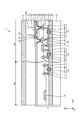
- FIG. 1 is a plan view schematically showing a display device according to the first embodiment.
- FIG. 2 is a circuit diagram showing a pixel circuit of a display device.
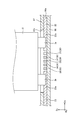
- FIG. 3 is a cross-sectional view taken along the line III-III'of FIG.
- FIG. 4 is an enlarged view of the connection portion between the array substrate and the light emitting element.
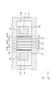
- FIG. 5 is a plan view of FIG.
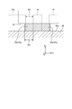
- FIG. 6 is a diagram showing a state in which the fifth auxiliary pad of the first embodiment is crushed by the anode 3b.
- FIG. 7 is a view when the center of the light emitting element in the first direction is misaligned toward the first pad and mounted.
- FIG. 1 is a plan view schematically showing a display device according to the first embodiment.
- FIG. 2 is a circuit diagram showing a pixel circuit of a display device.
- FIG. 3 is a cross-sectional view taken along the line III-III'of FIG.
- FIG. 4 is an enlarged view of the
- FIG. 8 is a view when the center of the light emitting element in the first direction is misaligned toward the second pad and mounted.
- FIG. 9 is an enlarged view of an enlarged connection portion between the array substrate and the light emitting element in the display device according to the second embodiment.
- FIG. 10 is an enlarged view showing a state before the light emitting element is bonded to the array substrate in the display device according to the third embodiment.
- FIG. 11 is an enlarged view showing a state in which a light emitting element is bonded to an array substrate in the display device according to the third embodiment.
- FIG. 12 is a plan view of the auxiliary pad according to the first modification.
- FIG. 13 is a plan view of the auxiliary pad according to the second modification.
- FIG. 14 is a plan view of the auxiliary pad according to the third modification.
- FIG. 15 is a plan view of the auxiliary pad according to the modified example 4 in a plan view.
- FIG. 16 is a plan view of the auxiliary pad according to the modified example 5 in a plan view.
- FIG. 17 is a plan view of the auxiliary pad according to the modified example 6 in a plan view.
- FIG. 1 is a plan view schematically showing a display device according to the first embodiment.
- the display device 1 includes an array substrate 2, a plurality of pixel Pix, a drive circuit 12, a drive IC (Integrated Circuit) 200, and a cathode wiring 26.
- the array board 2 is a wiring board for driving each pixel Pix.
- the array substrate 2 is also referred to as a backplane or active matrix substrate.
- the wiring board of the present disclosure is not limited to the array board 2.
- the array substrate 2 includes a substrate 21, a first transistor Tr1, a second transistor Tr2, etc., a transistor TrG (see FIG. 4), various wirings, and the like.
- the first transistor Tr1, the second transistor Tr2, and the like are switching elements provided for each pixel Pix.
- the transistor TrG is a switching element included in the drive circuit 12.
- the display device 1 has a display area AA and a peripheral area GA.
- the display area AA is an area that is arranged so as to overlap the plurality of pixels Pix and displays an image.
- the peripheral area GA is an area that does not overlap with the plurality of pixels Pix, and is arranged outside the display area AA.
- the plurality of pixel Pix are arranged in the first direction Dx and the second direction Dy in the display area AA of the substrate 21.
- the first direction Dx and the second direction Dy are directions parallel to the surface of the substrate 21.
- the direction parallel to the surface including the first direction Dx and the second direction Dy may be referred to as a plane direction.
- the first direction Dx is orthogonal to the second direction Dy. Therefore, the second direction Dy may be referred to as an orthogonal direction.
- the first direction Dx includes a case where the first direction Dx intersects the second direction Dy without being orthogonal to each other.
- the third direction Dz is a direction orthogonal to the first direction Dx and the second direction Dy, and may be referred to as a stacking direction.
- the drive circuit 12 is a circuit that drives a plurality of gate lines based on various control signals from the drive IC 200.
- the plurality of gate lines include the first gate line GCL1 and the second gate line GCL2 shown in FIG.
- the drive circuit 12 selects a plurality of gate lines sequentially or simultaneously, and supplies a gate drive signal to the selected gate lines. As a result, the drive circuit 12 selects a plurality of pixel Pix connected to the gate line.
- the drive IC 200 is a circuit that controls the display of the display device 1.
- the drive IC 200 is mounted as a COG (Chip On Glass) in the peripheral region GA of the substrate 21.
- the drive IC 200 may be mounted as a COF (Chip On Film) on a flexible printed circuit board or a rigid substrate connected to the peripheral region GA of the substrate 21.
- the cathode wiring 26 is provided in the peripheral region GA of the substrate 21.
- the cathode wiring 26 is provided so as to surround the plurality of pixels Pix in the display area AA and the drive circuit 12 in the peripheral area GA.
- the cathodes of the plurality of light emitting elements 3 are connected to a common cathode wiring 26, and for example, a ground potential is supplied.
- Pixel Pix has a light emitting element 3.
- the light emitting element 3 is provided corresponding to the pixel Pix, and includes a first light emitting element 3R, a second light emitting element 3G, and a third light emitting element 3B that emit light of different colors.
- the first light emitting element 3R emits red light.
- the second light emitting element 3G emits green light.
- the third light emitting element 3B emits blue light.
- the pixel Pix may include four or more light emitting elements 3 and emit four or more different colors of light.
- the pixel Pix is arranged repeatedly in the first direction Dx in the order of the pixel Pix having the first light emitting element 3R, the pixel Pix having the second light emitting element 3G, and the pixel Pix having the third light emitting element 3B. That is, the first light emitting element 3R, the second light emitting element 3G, and the third light emitting element 3B are repeatedly arranged in the first direction Dx in this order. Further, a plurality of the first light emitting element 3R, the second light emitting element 3G, and the third light emitting element 3B are arranged in the second direction Dy, respectively.
- the light emitting element 3 is an inorganic light emitting diode (LED: Light Emitting Diode) chip having a size of about 3 ⁇ m or more and 300 ⁇ m or less in a plan view, and is called a micro LED.
- a display device provided with a micro LED in each pixel is also called a micro LED display device.
- the micro of the micro LED does not limit the size of the inorganic light emitting diode. Further, the light emitting element 3 may be a mini LED.
- FIG. 2 is a circuit diagram showing a pixel circuit of a display device.
- the pixel circuit 28 is a drive circuit that drives the light emitting element 3.
- the pixel circuit 28 includes a plurality of switching elements (first transistor Tr1, second transistor Tr2, third transistor Tr3 and fourth transistor Tr4), a first gate line GCL1 and a second gate line GCL2. , Signal line SGL and power line LVdd.
- Each transistor is a thin film transistor (TFT).
- the first transistor Tr1 is a driving TFT.
- the second transistor Tr2 is a TFT for switching between a light emitting period and a non-light emitting period.
- the third transistor Tr3 and the fourth transistor Tr4 are current switching TFTs.
- the signal line SGL is connected to a constant current source.
- the power line LVdd is connected to a constant voltage source.
- a holding capacitance CS1 is formed between the drain of the second transistor Tr2 and the anode of the light emitting element 3. Further, a holding capacitance CS2 is formed between the anode of the light emitting element 3 and the power supply line LVdd.
- the pixel circuit 28 suppresses fluctuations in the gate voltage due to the parasitic capacitance of the second transistor Tr2 and the leakage current by the stray capacitance CS1 and the stray capacitance CS2.
- the drive circuit 12 sets the potential of the first gate line GCL1 to a high level and the potential of the second gate line GCL2 to a low level.
- the second transistor Tr2 and the third transistor Tr3 are turned on, and the fourth transistor Tr4 is turned off.
- a current Idata is supplied from the signal line SGL to the anode of the light emitting element 3.
- the drive circuit 12 sets the potential of the first gate line GCL1 to a low level and the potential of the second gate line GCL2 to a high level.
- the second transistor Tr2 and the third transistor Tr3 are turned off, and the fourth transistor Tr4 is turned on.
- a current Id is supplied to the anode of the light emitting element 3 from the constant power supply line LVdd.
- FIG. 2 is just an example, and the configuration of the pixel circuit 28 and the operation of the display device 1 can be appropriately changed.
- FIG. 3 is a cross-sectional view taken along the line III-III'of FIG. As shown in FIG. 3, the light emitting element 3 is provided on the array substrate 2.
- the array substrate 2 has a substrate 21, switching elements such as a first transistor Tr1 and a second transistor Tr2, various wirings, and various insulating films.
- Transistors TrG included in the drive circuit 12 are provided as a plurality of transistors in the peripheral region GA of the substrate 21.
- the substrate 21 is an insulating substrate, and for example, a glass substrate, a resin substrate, a resin film, or the like is used.
- the direction from the substrate 21 toward the upper surface 27a of the flattening film 27 in the direction perpendicular to the surface of the substrate 21 is referred to as "upper side”. Further, the direction from the upper surface 27a of the flattening film 27 toward the substrate 21 is defined as the “lower side”. Further, the “planar view” indicates a case where the substrate 21 is viewed from a direction perpendicular to the surface of the substrate 21.
- the first transistor Tr1, the second transistor Tr2, and the transistor TrG are provided on one surface side of the substrate 21.
- the first transistor Tr1 includes a semiconductor 61, a source electrode 62, a drain electrode 63, a first gate electrode 64A, and a second gate electrode 64B.
- the first gate electrode 64A is provided on the substrate 21 via the first insulating film 91.
- an inorganic insulating material such as a silicon oxide film (SiO), a silicon nitride film (SiN) or a silicon oxide nitride film (SiON) is used.
- each inorganic insulating film is not limited to a single layer and may be a laminated film.
- the second insulating film 92 is provided on the first insulating film 91 so as to cover the first gate electrode 64A.
- the semiconductor 61 is provided on the second insulating film 92.
- the third insulating film 93 covers the semiconductor 61 and is provided on the second insulating film 92.
- the second gate electrode 64B is provided on the third insulating film 93.
- the semiconductor 61 is provided between the first gate electrode 64A and the second gate electrode 64B in the third direction Dz. In the semiconductor 61, a channel region is formed in a portion sandwiched between the first gate electrode 64A and the second gate electrode 64B.
- the first transistor Tr1 has a so-called dual gate structure.
- the first transistor Tr1 may have a bottom gate structure in which the first gate electrode 64A is provided and the second gate electrode 64B is not provided, and the first gate electrode 64A is not provided and only the second gate electrode 64B is provided.
- the top gate structure may be used.
- the semiconductor 61 is composed of, for example, amorphous silicon, microcrystalline oxide semiconductor, amorphous oxide semiconductor, polysilicon, low temperature polysilicon (LTPS: Low Temperature Polycrystalline Silicone) or gallium nitride (GaN).
- oxide semiconductors include IGZO, zinc oxide (ZnO), and ITZO.
- IGZO is an indium gallium zinc oxide.
- ITZO is an indium tin oxide zinc oxide.
- the fourth insulating film 94 is provided on the third insulating film 93 so as to cover the second gate electrode 64B.
- the source electrode 62 and the drain electrode 63 are provided on the fourth insulating film 94.
- the source electrode 62 is electrically connected to the semiconductor 61 via the contact hole H5.
- the drain electrode 63 is electrically connected to the semiconductor 61 via the contact hole H3.
- the fifth insulating film 95 is provided on the fourth insulating film 94 so as to cover the source electrode 62 and the drain electrode 63.
- the fifth insulating film 95 is a flattening film that flattens the irregularities formed by the first transistor Tr1 and various wirings.
- the second transistor Tr2 includes a semiconductor 65, a source electrode 66, a drain electrode 67, a first gate electrode 68A, and a second gate electrode 68B.
- the second transistor Tr2 has a layer structure similar to that of the first transistor Tr1, and detailed description thereof will be omitted.
- the drain electrode 67 of the second transistor Tr2 is connected to the connection wiring 69 via the contact hole H8.
- the connection wiring 69 is connected to the first gate electrode 64A and the second gate electrode 64B of the first transistor Tr1.
- the semiconductor 65, the source electrode 66, the drain electrode 67, the first gate electrode 68A, and the second gate electrode 68B are the semiconductor 61, the source electrode 62, the drain electrode 63, and the first gate electrode 64A of the first transistor Tr1, respectively.
- the second gate electrode 64B is provided in the same layer, but may be provided in a different layer.
- the transistor TrG includes a semiconductor 71, a source electrode 72, a drain electrode 73, a first gate electrode 74A, and a second gate electrode 74B.
- the transistor TrG is a switching element included in the drive circuit 12.
- the transistor TrG also has a layer structure similar to that of the first transistor Tr1, and detailed description thereof will be omitted.
- the third transistor Tr3 and the fourth transistor Tr4 also have a layer structure similar to that of the first transistor Tr1.
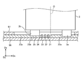
- FIG. 4 is an enlarged view of the connection portion between the array substrate and the light emitting element.
- the light emitting element 3 has a light emitting layer in which an n-type clad layer, an active layer, and a p-type clad layer are laminated in this order, and for example, a compound semiconductor such as gallium nitride (GaN) or aluminum indium phosphide (AlInP) is used.
- the light emitting element 3 has a so-called face-down structure in which a cathode 3a connected to the n-type clad layer and an anode 3b are provided on the p-type clad layer on the lower side.
- a known LED chip can be used as the light emitting element 3.
- the array substrate 2 has a first electrode 22, a second electrode 23, a third electrode 24, a fourth electrode 25, and a plurality of auxiliary pads 30.
- the first electrode 22 and the second electrode 23 are provided between the substrate 21 and the light emitting element 3.
- the first electrode 22 is provided on the first surface 96a of the sixth insulating film 96, and is electrically connected to the cathode wiring 26 (see FIG. 1) provided in the peripheral region GA. Further, as shown in FIG. 4, the first electrode 22 is connected to the cathode 3a of the light emitting element 3.
- the first electrode 22 has a first pad 22a as an electrode to be joined to the cathode 3a of the light emitting element 3.
- the first pad 22a is joined to the cathode 3a of the light emitting element 3 by welding. That is, at the time of joining, the first pad 22a is heated by a laser device or the like and melts. After that, the end portion of the cathode 3a of the light emitting element 3 is pushed into the melted first pad 22a to join them.
- the first pad 22a may be called a cathode pad.
- the second electrode 23 is connected to the anode 3b of the light emitting element 3.
- the second electrode 23 has a second pad 23a as an electrode for joining with the anode 3b of the light emitting element 3.
- the second pad 23a is joined to the anode 3b of the light emitting element 3 by welding.
- the second pad 23a may be referred to as an anode pad.
- the second electrode 23 is provided on the first surface 96a of the sixth insulating film 96. As shown in FIG. 3, the second electrode 23 is connected to the third electrode 24 via the contact hole H7.
- the third electrode 24 is provided on the fifth insulating film 95 and is connected to the drain electrode 63 via the contact hole H2. In this way, the second electrode 23 and the third electrode 24 connect the anode of the light emitting element 3 and the drain electrode 63 of the first transistor Tr1. Further, the fourth electrode 25 is provided in the same layer as the third electrode 24, and is connected to the source electrode 62 via the contact hole H4.
- the fourth electrode 25 extends on the fifth insulating film 95 and faces the first electrode 22 via the sixth insulating film 96 in the third direction Dz. As a result, a capacitance is formed between the first electrode 22 and the fourth electrode 25. The capacitance formed between the first electrode 22 and the fourth electrode 25 is used as the holding capacitance CS of the pixel circuit 28.
- the seventh insulating film 97 is provided on the first electrode 22, the second electrode 23, and the sixth insulating film 96. Further, the seventh insulating film 97 has an opening 97a for enabling connection between the first electrode 22, the second electrode 23, and the light emitting element 3.
- a flattening film 27 is provided on the seventh insulating film 97.
- the flattening film 27 is provided from the display region AA to the peripheral region GA.
- the flattening film 27 is a translucent organic insulating film, and for example, a resin material such as a silicone resin, an epoxy resin, an acrylic resin, or a polyimide resin is used. Further, on the flattening film 27, a cover portion 5 made of a member that transmits light, such as glass, is provided.
- the auxiliary pad 30 is manufactured of a conductive material and has conductivity. Further, in the present embodiment, the auxiliary pad 30 is manufactured of a metal material that is melted by heating of a laser device or the like.
- the auxiliary pad 30 is provided on the first surface 96a of the sixth insulating film 96.
- the auxiliary pad 30 is arranged between the first pad 22a and the second pad 23a, and is arranged in the vicinity of the edges of the first pad 22a and the second pad 23a.
- the vicinity of the edges of the first pad 22a and the second pad 23a is arranged in a range exposed from the opening 97a of the seventh insulating film 97, and has an insulating property with the first pad 22a and the second pad 23a.
- first pad 22a and the second pad 23a are separated from the edges to the extent that they can be secured. This is because if the auxiliary pad 30 is not exposed from the opening 97a of the seventh insulating film 97, the anode 3b and the like cannot be electrically connected to the auxiliary pad 30 when the light emitting element 3 is mounted on the array substrate 2.
- FIG. 5 is a plan view of FIG. As shown in FIG. 5, the distance W1 between the first pad 22a and the second pad 23a is larger than the width W2 of the first direction Dx of the cathode 3a and the anode 3b of the light emitting element 3. Therefore, even if the mounting position of the light emitting element 3 is displaced in the first direction Dx, it is avoided that the cathode 3a or the anode 3b is connected across the first pad 22a and the second pad 23a. It has become.
- Each auxiliary pad 30 has a rectangular shape that is longer in the second direction Dy than the first direction Dx when viewed from the third direction Dz. Further, each auxiliary pad 30 is in an island shape and is in an electrically floating state in the pre-process in which the light emitting element 3 is mounted.
- the five auxiliary pads 30 are arranged in the first direction Dx with an interval W3.
- the first auxiliary pad 31, the second auxiliary pad 32, the third auxiliary pad 33, and the fourth auxiliary pad are arranged in this order from the first pad 22a to the second pad 23a. 34, may be referred to as a fifth auxiliary pad 35.
- the auxiliary pad 30 when explaining the properties common to the first auxiliary pad 31, the second auxiliary pad 32, the third auxiliary pad 33, the fourth auxiliary pad 34, and the fifth auxiliary pad 35, they are collectively referred to as the auxiliary pad 30. Call.
- the first pad 22a and the first auxiliary pad 31 are separated from each other in the first direction Dx.
- the distance between the first pad 22a and the first auxiliary pad 31 is the same as the distance between the five auxiliary pads 30 and is W3.
- the second pad 23a and the fifth auxiliary pad 35 are separated from each other in the first direction Dx.
- the distance between the second pad 23a and the fifth auxiliary pad 35 is W3. From the above, the distance between the first pad 22a, the first auxiliary pad 31, the second auxiliary pad 32, the third auxiliary pad 33, the fourth auxiliary pad 34, the fifth auxiliary pad 35, and the second pad 23a in the first direction Dx. Are all W3 and are evenly spaced.
- FIG. 6 is a diagram showing a state in which the fifth auxiliary pad of the first embodiment is crushed by the anode 3b.
- the auxiliary pad 30 is heated by a laser device or the like and melts. Therefore, as shown in FIG. 6, when the mounting position of the light emitting element 3 is displaced in the first direction Dx, the auxiliary pad 30 (see the fifth auxiliary pad 35 in FIG. 6) is crushed by the cathode 3a or the anode 3b. May be The light emitting elements 3 shown in FIGS. 4 and 5 are not displaced.
- the auxiliary pad 30 has a gap in the first direction Dx, when it is crushed by the cathode 3a or the anode 3b, the auxiliary pad 30 bulges in the first direction Dx. From the above, the auxiliary pad 30 generates a bulging portion 30a (see the bulging portion 35a in FIG. 6) that bulges in the first direction Dx due to the misalignment of the light emitting element 3.
- the bulging portion 30a (see the bulging portion 35a in FIG. 6) has a first bulging amount of W4 in the first direction Dx.
- the amount of swelling indicates the amount of swelling in one of the first directions Dx with reference to the auxiliary pad 30 before being crushed.
- the distance W3 between the first pad 22a, the second pad 23a, and the five auxiliary pads 30 is smaller than the first bulging amount W4. Therefore, when the bulging portion 30a is generated, the auxiliary pad 30 comes into contact with the first pad 22a or the second pad 23a adjacent to the first direction Dx, or another auxiliary pad 30.
- the array substrate 2 includes the substrate 21 to the seventh insulating film 97 covering the first electrode 22 and the second electrode 23.
- the array substrate 2 does not include the flattening film 27, the light emitting element 3, and the cover portion 5.
- FIG. 7 is a diagram when the center of the light emitting element in the first direction is misaligned toward the first pad and mounted.
- FIG. 8 is a view when the center of the light emitting element in the first direction is misaligned toward the second pad and mounted.
- the light emitting element 3 mounted on the array substrate 2 is displaced.
- the anode 3b of the light emitting element 3 is, for example, the fourth auxiliary pad 34 and the fifth auxiliary pad 35. Crush.
- the bulging portion of the fourth auxiliary pad 34 see the bulging portion 30a in FIG.
- the bulging portion (see FIG. 6) 35a generated in the fifth auxiliary pad 35 comes into contact with the second pad 23a adjacent to the first direction Dx. Further, as shown in FIG. 7, the second pad 23a is also crushed by the anode 3b. Therefore, the second pad 23a has a bulging portion 23b that bulges toward the fifth auxiliary pad 35, and the contact with the fifth auxiliary pad 35 is ensured. From the above, the portion of the anode 3b that is not in contact with the second pad 23a conducts with the second pad 23a via the fourth auxiliary pad 34 and the fifth auxiliary pad 35.
- the cathode 3a of the light emitting element is, for example, the first auxiliary pad 31 and the second auxiliary as shown in FIG. Crush the pad 32.
- the bulging portion of the second auxiliary pad 32 comes into contact with the first auxiliary pad 31 and the third auxiliary pad 33 adjacent to each other in the first direction Dx.
- the bulging portion of the first auxiliary pad 31 comes into contact with the first pad 22a adjacent to the first direction Dx.
- the first pad 22a is also crushed by the cathode 3a. Therefore, the first pad 22a has a bulging portion 22b that bulges toward the first auxiliary pad 31, and the contact with the first auxiliary pad 31 is ensured. From the above, the portion of the cathode 3a that is not in contact with the first pad 22a conducts with the first pad 22a via the first auxiliary pad 31 and the second auxiliary pad 32.
- the display device 1 and the array substrate (wiring substrate) 2 of the first embodiment even if the mounting position of the light emitting element 3 is displaced, the electrical resistance of the connection portion composed of the cathode 3a and the first pad 22a. Is suppressed. Further, an increase in electrical resistance of the connection portion including the anode 3b and the second pad 23a is suppressed.
- the bonding between the anode 3b and the cathode 3a and the pads is welding, but the wiring board and display device of the present disclosure are not limited to this.
- ACF Anisotropic Conductive Film
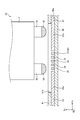
- FIG. 9 is an enlarged view of an enlarged connection portion between the array substrate and the light emitting element in the display device according to the second embodiment.
- the display device 1A differs from the display device 1 of the first embodiment in that it has an anisotropic conductive film 40.
- the anisotropic conductive film 40 is arranged so as to straddle the first pad 22a, the plurality of auxiliary pads 30, and the second pad 23a.
- the intervals between the first pad 22a, the plurality of auxiliary pads 30, and the first direction Dx in the second pad 23a are W5, which are equal intervals.
- the anisotropic conductive film 40 includes a plurality of metal particles 42 inside the sheet-shaped thermosetting resin 41, and has conductivity in the third direction Dz.
- the anisotropic conductive film 40 is arranged so as to straddle the first pad 22a, the plurality of auxiliary pads 30, and the second pad 23a before curing, and the first pad 22a, the plurality of auxiliary pads 30, and the second pad are arranged. It is welded to each of 23a. Further, in the anisotropic conductive film 40, before curing, the anode 3b and the cathode 3a of the light emitting element 3 are pushed in and welded to each of the anode 3b and the cathode 3a.
- the portion of the anode 3b and the cathode 3a that overlaps the first pad 22a and the second pad 23a when viewed from the third direction Dz is the first pad 22a via the metal particles 42.
- the second pad 23a is conductive.
- the distance W5 of the first direction Dx between the first pad 22a, the plurality of auxiliary pads 30, and the second pad 23a is smaller than the particle size of the metal particles 42. Therefore, when the center of the first direction Dx of the light emitting element 3 is displaced toward the first pad 22a, the metal particles 42 are pushed into the anode 3b and the anode 3b and the fourth auxiliary pad 34 are pushed as shown in FIG. It is interposed between the anode 3b and the fifth auxiliary pad 35. Further, the metal particles 42 are interposed between the 4th auxiliary pad 34 and the 5th auxiliary pad 35, and between the 5th auxiliary pad 35 and the 2nd pad 23a.
- the portion of the anode 3b that does not overlap with the second pad when viewed from the third direction Dz is electrically connected to the fourth auxiliary pad 34 and the fifth auxiliary pad 35 via the metal particles 42, and the second pad Conducts with 23a. From the above, the increase in the electrical resistance of the connection portion can be suppressed even in the second embodiment.
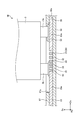
- FIG. 10 is an enlarged view showing a state before the light emitting element is bonded to the array substrate in the display device according to the third embodiment.
- FIG. 11 is an enlarged view showing a state in which a light emitting element is bonded to an array substrate in the display device according to the third embodiment.
- the display device 1B of the third embodiment is different from the display device 1 of the first embodiment and the display device 1B of the second embodiment in that it has the conductive material 50.
- the conductive material 50 is a solder material such as Sn.
- the conductive material 50 is welded to the end faces of the anode 3b and the cathode 3a of the light emitting element 3.
- the conductive material 50 is heated and adheres to the end faces of the anode 3b and the cathode 3a in a molten state. Then, the anode 3b and the cathode 3a are pressed toward the first pad 22a and the second pad 23a while maintaining the molten state of the conductive material 50. When the conductive material 50 is cured, the anode 3b and the cathode 3a are joined to the first pad 22a and the second pad 23a.
- auxiliary pads arranged at equal intervals are given as an example, but the auxiliary pads of the present disclosure are not limited to this.
- An example of arranging the auxiliary pads will be described below.
- FIG. 12 is a plan view of the auxiliary pad according to the first modification.
- Four auxiliary pads 30A of the array substrate 2 according to the first modification are provided.
- the auxiliary pad 30A is different from the auxiliary pad 30 of the first embodiment in that it does not include the third auxiliary pad 33 (see FIG. 5).
- the distance W6 between the second auxiliary pad 32 and the fourth auxiliary pad 34 has a length that does not come into contact with each other even if it straddles the second auxiliary pad 32 and the fourth auxiliary pad 34 and is crushed by the anode 3b or the cathode 3a. It has become. In other words, the distance between the bulging portion 30a formed on the second auxiliary pad 32 (see FIG. 6) and the bulging portion 30a formed on the fourth auxiliary pad 34 (see FIG. 6) does not come into contact with each other. ing. That is, the interval W6 is longer than the length obtained by doubling the first bulging amount W4 of the bulging portion 30a.
- the second auxiliary pad 32 and the fourth auxiliary pad 34 are not electrically connected, and a short circuit between the first pad 22a and the second pad 23a can be reliably avoided. If the bonding method between the anode 3b and the like and the second pad and the like is not welding and the anisotropic conductive film 40 (see FIG. 9), the interval W6 is larger than the particle size of the metal particles 42, the insulating property. Is secured.
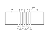
- FIG. 13 is a plan view of the auxiliary pad according to the second modification.
- Five auxiliary pads 30B of the array substrate 2 according to the second modification are provided as in the first embodiment.
- the distance between the first pad 22a and the first auxiliary pad 31 and the distance between the second pad 23a and the fifth auxiliary pad 35 are both W11.
- the distance between the first auxiliary pad 31 and the second auxiliary pad 32 and the distance between the fourth auxiliary pad 34 and the fifth auxiliary pad 35 are both W12.
- the distance between the second auxiliary pad 32 and the third auxiliary pad 33 and the distance between the third auxiliary pad 33 and the fourth auxiliary pad 34 are both W13.
- FIG. 14 is a plan view of the auxiliary pad according to the third modification.
- Five auxiliary pads 30C of the array substrate 2 according to the third modification are provided.
- the first auxiliary pad 31C, the second auxiliary pad 32C, the third auxiliary pad 33C, the fourth auxiliary pad 34C, and the fifth auxiliary pad 35C are respectively from one end to the other end of the second direction Dy in the first direction Dx. It has a wavy shape that protrudes alternately from one side to the other. Therefore, the auxiliary pad of the present disclosure is not limited to the rectangular shape, and may correspond to the shape of the edge portion of the first pad 22a and the second pad 23a.
- FIG. 15 is a plan view of the auxiliary pad according to the modified example 4 in a plan view.
- the auxiliary pad 30D of the array substrate 2 according to the modified example 4 is a square auxiliary pad 36 forming a square in a plan view.
- a plurality of square auxiliary pads 36 are provided, and are arranged at equal intervals in the first direction Dx and the second direction Dy. According to the square auxiliary pad 36, when it is crushed by the anode 3b or the cathode 3a, it bulges in the first direction Dx or the second direction Dy.
- FIG. 16 is a plan view of the auxiliary pad according to the modified example 5 in a plan view.
- the auxiliary pad 30E of the array substrate 2 according to the modified example 5 is composed of a plurality of peripheral auxiliary pads 37a, 37b, 37c, 37d, 38a, 38b, 38c, 38d that surround the first pad 22a and the second pad 23a.
- the peripheral auxiliary pads 37a and 37c sandwich the first pad 22a from the first direction Dx while being separated from the first pad 22a.
- the peripheral auxiliary pads 37b and 37d sandwich the first pad 22a from the second direction Dy while being separated from the first pad 22a.
- the peripheral auxiliary pads 38a and 38c sandwich the second pad 23a from the first direction Dx while being separated from the second pad 23a.
- the peripheral auxiliary pads 38b and 38d sandwich the second pad 23a from the second direction Dy while being separated from the second pad 23a.
- FIG. 17 is a plan view of the auxiliary pad according to the modified example 6 in a plan view.
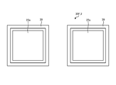
- the auxiliary pad 30F of the array substrate 2 according to the modification 6 is a rectangular frame-shaped auxiliary pad 39 that surrounds the periphery of the first pad 22a and the second pad 23a. Even with this frame-shaped auxiliary pad 39, the same effect as that of the modified example 5 can be obtained.
- the wiring board and the display device according to the embodiment and the modified example have been described above, if there is at least one auxiliary pad of the present disclosure, an increase in electrical resistance of the connection portion can be suppressed. Therefore, the wiring board and display device of the present disclosure also include one in which one auxiliary pad is arranged near the edge of the first pad 22a (cathode pad) or the second pad 23a (anode pad).
Landscapes
- Engineering & Computer Science (AREA)
- Microelectronics & Electronic Packaging (AREA)
- Devices For Indicating Variable Information By Combining Individual Elements (AREA)
- Electroluminescent Light Sources (AREA)
- Led Device Packages (AREA)
Abstract
配線基板は、基板と、前記基板に積層される絶縁膜と、前記絶縁膜の第1面に積層され、無機発光ダイオードのアノードと電気的に接続されるアノード用パッドと、前記絶縁膜の第1面に積層され、前記無機発光ダイオードのカソードと電気的に接続されるカソード用パッドと、前記絶縁膜の第1面に設けられ、かつ導電性を有する補助パッドと、を備え、前記補助パッドは、前記アノード用パッド又は前記カソード用パッドの縁部の近傍にフローティング状態で配置されている。
Description
本発明は、配線基板及び表示装置に関する。
特許文献1に示すように、表示装置として、無機発光ダイオード(ミニLEDやマイクロLED(micro LED))を用いた無機ELディスプレイが挙げられる。また、無機ELディスプレイは、配線基板として、薄膜トランジスタ(TFT:Thin Film Transistor)がアレイ状に配列したアレイ基板を備える。特許文献2や特許文献3に示すように、アレイ基板は、無機発光ダイオードのアノードとカソードとを接合するためのパッド(電極)を有している。よって、アノードとカソードとパッドは、アレイ基板と無機発光ダイオードとを接続する接続部を構成している。
配線基板(アレイ基板)に対する無機発光ダイオードの搭載位置がずれてしまうと、パッドに対するアノード又はカソードの接触面積が低減する。この結果、接続部の抵抗値が増加し、好ましくない。特に、ミニLEDやマイクロLEDなど小型化した部品において、位置ずれの許容範囲が狭く、接続部の抵抗値の増加を招き易い。
本発明は、無機発光ダイオードの搭載位置が所定の位置からずれても、接続部の抵抗値の増加を抑制できる配線基板及び表示装置を提供することを目的とする。
本発明の一態様の配線基板は、基板と、前記基板に積層される絶縁膜と、前記絶縁膜の第1面に積層され、無機発光ダイオードのアノードと電気的に接続されるアノード用パッドと、前記絶縁膜の第1面に積層され、前記無機発光ダイオードのカソードと電気的に接続されるカソード用パッドと、前記絶縁膜の第1面に設けられ、かつ導電性を有する補助パッドと、を備え、前記補助パッドは、前記アノード用パッド又は前記カソード用パッドの縁部の近傍にフローティング状態で配置されている。
本発明の一態様の表示装置は、前記配線基板と、溶融した前記アノード用パッド及び前記カソード用パッドに前記アノード及び前記カソードが押し付けて接合した無機発光ダイオードと、を備える。前記補助パッドは、前記平面方向に隣り合う前記アノード用パッド又は前記カソード用パッドに接続する、若しくは前記平面方向に隣り合う他の前記補助パッドに接続する、膨出部を有する。
本発明の一態様の表示装置は、前記配線基板と、複数の金属粒子を含み、前記アノード用パッド及び前記カソード用パッドと前記補助パッドに跨って積層された異方性導電フィルムと、溶融した前記異方性導電フィルムに前記アノードと前記カソードを押し付けて接合した無機発光ダイオードのアノードと、を備える。前記無機発光ダイオードは、複数の前記金属粒子を介して前記アノード用パッドと前記カソード用パッドと前記補助パッドと電気的に接続している。前記補助パッドは、複数の前記金属粒子を介して前記アノード用パッドと前記カソード用パッドと電気的に接続している。
発明を実施するための形態(実施形態)につき、図面を参照しつつ詳細に説明する。以下の実施形態に記載した内容により本発明が限定されるものではない。また、以下に記載した構成要素には、当業者が容易に想定できるもの、実質的に同一のものが含まれる。さらに、以下に記載した構成要素は適宜組み合わせることが可能である。なお、開示はあくまで一例にすぎず、当業者において、発明の主旨を保っての適宜変更について容易に想到し得るものについては、当然に本発明の範囲に含有されるものである。また、図面は説明をより明確にするため、実際の態様に比べ、各部の幅、厚さ、形状等について模式的に表される場合があるが、あくまで一例であって、本発明の解釈を限定するものではない。また、本明細書と各図において、既出の図に関して前述したものと同様の要素には、同一の符号を付して、詳細な説明を適宜省略することがある。
(実施形態1)
図1は、実施形態1に係る表示装置を模式的に示す平面図である。図1に示すように、表示装置1は、アレイ基板2と、複数の画素Pixと、駆動回路12と、駆動IC(Integrated Circuit)200と、カソード配線26と、を含む。アレイ基板2は、各画素Pixを駆動するための配線基板である。アレイ基板2は、バックプレーン又はアクティブマトリックス基板とも呼ばれる。なお、本開示の配線基板は、アレイ基板2に限定されない。アレイ基板2は、基板21と、第1トランジスタTr1、第2トランジスタTr2等と、トランジスタTrG(図4参照)と、各種配線等を含む。第1トランジスタTr1、第2トランジスタTr2等は、画素Pix毎に設けられたスイッチング素子である。トランジスタTrGは、駆動回路12に含まれるスイッチング素子である。
図1は、実施形態1に係る表示装置を模式的に示す平面図である。図1に示すように、表示装置1は、アレイ基板2と、複数の画素Pixと、駆動回路12と、駆動IC(Integrated Circuit)200と、カソード配線26と、を含む。アレイ基板2は、各画素Pixを駆動するための配線基板である。アレイ基板2は、バックプレーン又はアクティブマトリックス基板とも呼ばれる。なお、本開示の配線基板は、アレイ基板2に限定されない。アレイ基板2は、基板21と、第1トランジスタTr1、第2トランジスタTr2等と、トランジスタTrG(図4参照)と、各種配線等を含む。第1トランジスタTr1、第2トランジスタTr2等は、画素Pix毎に設けられたスイッチング素子である。トランジスタTrGは、駆動回路12に含まれるスイッチング素子である。
図1に示すように、表示装置1は、表示領域AAと、周辺領域GAとを有する。表示領域AAは、複数の画素Pixと重なって配置され、画像を表示する領域である。周辺領域GAは、複数の画素Pixと重ならない領域であり、表示領域AAの外側に配置される。
複数の画素Pixは、基板21の表示領域AAにおいて、第1方向Dx及び第2方向Dyに配列される。なお、第1方向Dx及び第2方向Dyは、基板21の表面に対して平行な方向である。第1方向Dxと第2方向Dyとを含む面と平行な方向を平面方向ということがある。第1方向Dxは、第2方向Dyと直交する。よって、第2方向Dyを直交方向という場合がある。ただし、第1方向Dxは、第2方向Dyと直交しないで交差する場合を含む。第3方向Dzは、第1方向Dx及び第2方向Dyと直交する方向であり、積層方向という場合がある。
駆動回路12は、駆動IC200からの各種制御信号に基づいて複数のゲート線を駆動する回路である。複数のゲート線には、図2に示す第1ゲート線GCL1及び第2ゲート線GCL2が含まれる。駆動回路12は、複数のゲート線を順次又は同時に選択し、選択されたゲート線にゲート駆動信号を供給する。これにより、駆動回路12は、ゲート線に接続された複数の画素Pixを選択する。
駆動IC200は、表示装置1の表示を制御する回路である。駆動IC200は、基板21の周辺領域GAにCOG(Chip On Glass)として実装される。これに限定されず、駆動IC200は、基板21の周辺領域GAに接続されたフレキシブルプリント基板やリジット基板の上にCOF(Chip On Film)として実装されてもよい。
カソード配線26は、基板21の周辺領域GAに設けられる。カソード配線26は、表示領域AAの複数の画素Pix及び周辺領域GAの駆動回路12を囲んで設けられる。複数の発光素子3のカソードは、共通のカソード配線26に接続され、例えば、グランド電位が供給される。
画素Pixは、発光素子3を有する。発光素子3は、画素Pixに対応して設けられ、異なる色の光を出射する第1発光素子3R、第2発光素子3G、及び第3発光素子3Bを含む。第1発光素子3Rは、赤色の光を出射する。第2発光素子3Gは、緑色の光を出射する。第3発光素子3Bは、青色の光を出射する。なお、以下の説明において、第1発光素子3R、第2発光素子3G及び第3発光素子3Bを区別して説明する必要がない場合には、単に発光素子3と表す。なお、画素Pixは、4つ以上の発光素子3を備え、4色以上の異なる光を出射してもよい。
画素Pixの配列は、第1発光素子3Rを有する画素Pix、第2発光素子3Gを有する画素Pix、第3発光素子3Bを有する画素Pix、の順で第1方向Dxに繰り返し配列される。つまり、第1発光素子3R、第2発光素子3G及び第3発光素子3Bは、この順で第1方向Dxに繰り返し配列される。また、第1発光素子3R、第2発光素子3G及び第3発光素子3Bは、それぞれ第2方向Dyに複数配列される。
発光素子3は、平面視で、3μm以上、300μm以下程度の大きさを有する無機発光ダイオード(LED:Light Emitting Diode)チップであり、マイクロLED(micro LED)と呼ばれる。各画素にマイクロLEDを備える表示装置は、マイクロLED表示装置とも呼ばれる。なお、マイクロLEDのマイクロは、無機発光ダイオードの大きさを限定するものではない。また、発光素子3は、ミニLEDであってもよい。
図2は、表示装置の画素回路を示す回路図である。画素回路28は、発光素子3を駆動する駆動回路である。図2に示すように、画素回路28は、複数のスイッチング素子(第1トランジスタTr1、第2トランジスタTr2、第3トランジスタTr3及び第4トランジスタTr4)と、第1ゲート線GCL1、第2ゲート線GCL2、信号線SGL及び電源線LVddを有する。各トランジスタは、それぞれ薄膜トランジスタ(TFT:Thin Film Transistor)である。
第1トランジスタTr1は駆動用TFTである。第2トランジスタTr2は、発光期間と、非発光期間とのスイッチング用TFTである。第3トランジスタTr3及び第4トランジスタTr4は、電流切替用TFTである。信号線SGLは、定電流源に接続されている。電源線LVddは、定電圧源に接続されている。
また、第2トランジスタTr2のドレインと、発光素子3のアノードとの間に保持容量CS1が形成される。また、発光素子3のアノードと電源線LVddとの間に保持容量CS2が形成される。画素回路28は、保持容量CS1と保持容量CS2により、第2トランジスタTr2の寄生容量とリーク電流とによるゲート電圧の変動を抑制する。
非発光期間では、駆動回路12(図1参照)は、第1ゲート線GCL1の電位を高レベルとし、第2ゲート線GCL2の電位を低レベルとする。これにより、第2トランジスタTr2及び第3トランジスタTr3がオンとなり、第4トランジスタTr4がオフとなる。発光素子3のアノードには、信号線SGLから電流Idataが供給される。
発光期間では、駆動回路12(図1参照)は、第1ゲート線GCL1の電位を低レベルとし、第2ゲート線GCL2の電位を高レベルとする。これにより、第2トランジスタTr2及び第3トランジスタTr3がオフとなり、第4トランジスタTr4がオンとなる。発光素子3のアノードには、定電源線LVddから電流Idが供給される。なお、図2は、あくまで一例であり、画素回路28の構成及び表示装置1の動作は適宜変更することができる。
図3は、図1のIII-III’線の矢視断面図である。図3に示すように、発光素子3は、アレイ基板2の上に設けられる。アレイ基板2は、基板21と、第1トランジスタTr1、第2トランジスタTr2等のスイッチング素子と、各種配線及び各種絶縁膜を有する。基板21の周辺領域GAには、複数のトランジスタとして、駆動回路12に含まれるトランジスタTrGが設けられている。基板21は絶縁基板であり、例えば、ガラス基板、樹脂基板又は樹脂フィルム等が用いられる。
本明細書において、基板21の表面に垂直な方向において、基板21から平坦化膜27の上面27aに向かう方向を「上側」とする。また、平坦化膜27の上面27aから基板21に向かう方向を「下側」とする。また、「平面視」とは、基板21の表面に垂直な方向から見た場合を示す。
第1トランジスタTr1、第2トランジスタTr2、及びトランジスタTrGは、基板21の一方の面側に設けられる。第1トランジスタTr1は、半導体61、ソース電極62、ドレイン電極63、第1ゲート電極64A及び第2ゲート電極64Bを含む。第1ゲート電極64Aは、第1絶縁膜91を介して基板21の上に設けられる。第1絶縁膜91等の絶縁膜は、シリコン酸化膜(SiO)、シリコン窒化膜(SiN)又はシリコン酸化窒化膜(SiON)等の無機絶縁材料が用いられる。また、各無機絶縁膜は、単層に限定されず積層膜であってもよい。
第2絶縁膜92は、第1ゲート電極64Aを覆って第1絶縁膜91の上に設けられる。半導体61は、第2絶縁膜92の上に設けられる。第3絶縁膜93は、半導体61を覆って第2絶縁膜92の上に設けられる。第2ゲート電極64Bは、第3絶縁膜93の上に設けられる。半導体61は、第3方向Dzにおいて、第1ゲート電極64Aと第2ゲート電極64Bとの間に設けられる。半導体61において、第1ゲート電極64A及び第2ゲート電極64Bで挟まれた部分にチャネル領域が形成される。
図3に示す例では、第1トランジスタTr1は、いわゆるデュアルゲート構造である。ただし、第1トランジスタTr1は、第1ゲート電極64Aが設けられ、第2ゲート電極64Bが設けられないボトムゲート構造でもよく、第1ゲート電極64Aが設けられず、第2ゲート電極64Bのみが設けられるトップゲート構造でもよい。
半導体61は、例えば、アモルファスシリコン、微結晶酸化物半導体、アモルファス酸化物半導体、ポリシリコン、低温ポリシリコン(LTPS:Low Temperature Polycrystalline Silicone)又は窒化ガリウム(GaN)で構成される。酸化物半導体としては、IGZO、酸化亜鉛(ZnO)、ITZOが例示される。IGZOは、インジウムガリウム亜鉛酸化物である。ITZOは、インジウムスズ亜鉛酸化物である。
第4絶縁膜94は、第2ゲート電極64Bを覆って第3絶縁膜93の上に設けられる。ソース電極62及びドレイン電極63は、第4絶縁膜94の上に設けられる。本実施形態では、ソース電極62は、コンタクトホールH5を介して半導体61と電気的に接続される。ドレイン電極63は、コンタクトホールH3を介して半導体61と電気的に接続される。
第5絶縁膜95は、ソース電極62及びドレイン電極63を覆って、第4絶縁膜94の上に設けられる。第5絶縁膜95は、第1トランジスタTr1や、各種配線で形成される凹凸を平坦化する平坦化膜である。
第2トランジスタTr2は、半導体65、ソース電極66、ドレイン電極67、第1ゲート電極68A及び第2ゲート電極68Bを含む。第2トランジスタTr2は第1トランジスタTr1と類似した層構成を有しており、詳細な説明は省略する。第2トランジスタTr2のドレイン電極67は、コンタクトホールH8を介して接続配線69に接続される。接続配線69は、第1トランジスタTr1の、第1ゲート電極64A及び第2ゲート電極64Bに接続される。
なお、半導体65、ソース電極66、ドレイン電極67、第1ゲート電極68A及び第2ゲート電極68Bは、それぞれ、第1トランジスタTr1の、半導体61、ソース電極62、ドレイン電極63、第1ゲート電極64A及び第2ゲート電極64Bと同層に設けられているが、異なる層に設けられていてもよい。
トランジスタTrGは、半導体71、ソース電極72、ドレイン電極73、第1ゲート電極74A及び第2ゲート電極74Bを含む。トランジスタTrGは、駆動回路12に含まれるスイッチング素子である。トランジスタTrGも第1トランジスタTr1と類似した層構成を有しており、詳細な説明は省略する。また、第3トランジスタTr3及び第4トランジスタTr4(図2参照)も第1トランジスタTr1と類似した層構成を有する。
図4は、アレイ基板と発光素子との接続部を拡大した拡大図である。発光素子3は、n型クラッド層、活性層、p型クラッド層が順に積層された発光層を有し、例えば、窒化ガリウム(GaN)、アルミニウムインジウム燐(AlInP)等の化合物半導体が用いられる。図4に示すように、発光素子3は、n型クラッド層に接続するカソード3aと、p型クラッド層にアノード3bと、が下側に設けられた、いわゆるフェースダウン構造である。なお、発光素子3は公知のLEDチップを用いることができる。
図3に示すように、アレイ基板2は、第1電極22、第2電極23、第3電極24、第4電極25、及び複数の補助パッド30を有する。
第1電極22及び第2電極23は、基板21と発光素子3との間に設けられる。第1電極22は、第6絶縁膜96の第1面96aに設けられ、周辺領域GAに設けられたカソード配線26(図1参照)に電気的に接続される。また、図4に示すように、第1電極22は、発光素子3のカソード3aと接続される。第1電極22は、発光素子3のカソード3aと接合する電極として、第1パッド22aを有する。第1パッド22aは、発光素子3のカソード3aと溶着により接合している。つまり、接合時、第1パッド22aは、レーザ装置等により加熱されて溶融する。その後、溶融している第1パッド22aに発光素子3のカソード3aの端部が押し込まれて接合している。なお、第1パッド22aは、カソード用パッドと呼ばれることがある。
第2電極23は、発光素子3のアノード3bと接続される。第2電極23は、発光素子3のアノード3bと接合する電極として、第2パッド23aを有する。第2パッド23aは、カソード3aと同様に、発光素子3のアノード3bと溶着により接合している。なお、第2パッド23aは、アノード用パッドと呼ばれることがある。また、第2電極23は、第6絶縁膜96の第1面96aに設けられる。第2電極23は、図3に示すように、コンタクトホールH7を介して第3電極24と接続される。
第3電極24は、第5絶縁膜95の上に設けられ、コンタクトホールH2を介してドレイン電極63と接続される。このように、第2電極23及び第3電極24は、発光素子3のアノードと、第1トランジスタTr1のドレイン電極63とを接続する。また、第4電極25は第3電極24と同層に設けられ、コンタクトホールH4を介してソース電極62と接続される。
第4電極25は、第5絶縁膜95の上で延在して、第3方向Dzにおいて第6絶縁膜96を介して第1電極22と対向する。これにより、第1電極22と第4電極25との間に容量が形成される。第1電極22と第4電極25との間に形成される容量は、画素回路28の保持容量CSとして用いられる。
第7絶縁膜97は、第1電極22と、第2電極23と、第6絶縁膜96との上に設けられる。また、第7絶縁膜97は、第1電極22及び第2電極23と、発光素子3と、の接続を可能とするための開口97aを有している。
第7絶縁膜97の上には、平坦化膜27が設けられている。平坦化膜27は、表示領域AAから周辺領域GAに亘って設けられている。平坦化膜27は、透光性を有する有機絶縁膜であり、例えば、シリコーン樹脂、エポキシ樹脂、アクリル樹脂、ポリイミド樹脂等の樹脂材料が用いられる。また、平坦化膜27の上には、例えばガラスなど、光を透過する部材で構成されるカバー部5が設けられている。
図4に示すように、補助パッド30は、導電性材料により製造されており、導電性を有している。また、本実施形態では、補助パッド30は、レーザ装置等の加熱により溶融する金属材料により製造されている。補助パッド30は、第6絶縁膜96の第1面96aに設けられている。補助パッド30は、第1パッド22aと第2パッド23aとの間に配置され、第1パッド22a及び第2パッド23aの縁部の近傍に配置されている。なお、第1パッド22a及び第2パッド23aの縁部の近傍とは、第7絶縁膜97の開口97aから露出した範囲に配置され、かつ第1パッド22a及び第2パッド23aとの絶縁性を確保できる程度に第1パッド22a及び第2パッド23aの縁部から離隔している、という意味である。なお、補助パッド30が第7絶縁膜97の開口97aから露出していないと、アレイ基板2に発光素子3を搭載する際、アノード3b等が補助パッド30と電気的に接続できないからである。
図5は、図4の平面図である。図5に示すように、第1パッド22aと第2パッド23aとの間の距離W1は、発光素子3のカソード3a及びアノード3bの第1方向Dxの幅W2よりも大きい。よって、仮に発光素子3の搭載位置が第1方向Dxにずれしたとしても、カソード3a又はアノード3bが第1パッド22aと第2パッド23aとに跨って接続する、ということが回避されるようになっている。
補助パッド30は、5つ設けられている。各補助パッド30は、第3方向Dzから視た場合、第1方向Dxよりも第2方向Dyに長い長方形状を成している。また、各補助パッド30は発光素子3が実装される前工程において、島状であり、電気的にフローティングな状態である。5つの補助パッド30は、間隔W3を空けながら、第1方向Dxに配列している。以下、必要に応じて、5つの補助パッド30について、第1パッド22aから第2パッド23aに向かって順に、第1補助パッド31、第2補助パッド32、第3補助パッド33、第4補助パッド34、第5補助パッド35、と呼ぶ場合がある。また、第1補助パッド31、第2補助パッド32、第3補助パッド33、第4補助パッド34、及び第5補助パッド35において共通する性質を説明する場合には、総称して補助パッド30と呼ぶ。
第1パッド22aと第1補助パッド31とは、第1方向Dxに離隔している。第1パッド22aと第1補助パッド31との間隔は、5つの補助パッド30の間隔と同じでW3となっている。同様に、第2パッド23aと第5補助パッド35とは、第1方向Dxに離隔している。第2パッド23aと第5補助パッド35との間隔はW3となっている。以上から、第1パッド22a、第1補助パッド31、第2補助パッド32、第3補助パッド33、第4補助パッド34、第5補助パッド35、及び第2パッド23aにおける第1方向Dxの間隔は、全てW3であり、等間隔となっている。
図6は、実施形態1の第5補助パッドがアノード3bに押し潰された状態を示す図である。補助パッド30は、アレイ基板2に対し発光素子3を搭載する際、レーザ装置等により加熱されて溶融する。よって、図6に示すように、発光素子3の搭載位置が第1方向Dxにずれた場合、補助パッド30(図6の第5補助パッド35を参照)は、カソード3a又はアノード3bに押し潰される可能性がある。なお、図4、図5に示す発光素子3は位置ずれしていない。また、補助パッド30は、第1方向Dxに隙間があることから、カソード3a又はアノード3bによる押し潰された場合、第1方向Dxへ膨出する。以上から、補助パッド30は、発光素子3の位置ずれにより、第1方向Dxに膨出する膨出部30a(図6の膨出部35aを参照)が発生する。
また、膨出部30a(図6の膨出部35aを参照)は、第1方向Dxへの第1膨出量がW4となっている。なお、膨出量は、潰される前の補助パッド30を基準として第1方向Dxの一方に膨らんだ量を示す。一方で、第1パッド22aと第2パッド23aと5つの補助パッド30のそれぞれの間隔W3は、第1膨出量W4よりも小さい。よって、補助パッド30は、膨出部30aが発生すると、第1方向Dxに隣り合う第1パッド22a又は第2パッド23a、或は他の補助パッド30と接触する。
なお、上記した表示装置1において、アレイ基板2は、基板21から第1電極22及び第2電極23を覆う第7絶縁膜97までを含む。アレイ基板2には、平坦化膜27、発光素子3、カバー部5は含まれない。
図7は、発光素子における第1方向の中心が第1パッド寄りに位置ずれして搭載された場合の図である。図8は、発光素子における第1方向の中心が第2パッド寄りに位置ずれして搭載された場合の図である。次に、アレイ基板2に搭載する発光素子3が位置ずれした場合を説明する。図7に示すように、発光素子3の第1方向Dxの中心Oが第1パッド22a寄りとなった場合、発光素子3のアノード3bは、例えば、第4補助パッド34と第5補助パッド35を押し潰す。これにより、第4補助パッド34の膨出部(図6の膨出部30aを参照)は、隣り合う第3補助パッド33と第5補助パッド35と接触する。また、第5補助パッド35に発生した膨出部(図6参照)35aは、第1方向Dxに隣り合う第2パッド23aと接触する。さらに、図7に示すように、第2パッド23aもアノード3bに押し潰されている。よって、第2パッド23aは、第5補助パッド35に向かって膨出する膨出部23bが生じ、第5補助パッド35との接触が確実となっている。以上から、アノード3bにおいて第2パッド23aに接触していない部分は、第4補助パッド34及び第5補助パッド35を介して第2パッド23aと導通する。
一方で、発光素子3の第1方向Dxの中心Oが第2パッド23a寄りとなった場合、発光素子のカソード3aは、図8に示すように、例えば、第1補助パッド31、第2補助パッド32を押し潰す。これにより、第2補助パッド32の膨出部(図6の膨出部30aを参照)は、第1方向Dxに隣り合う第1補助パッド31と第3補助パッド33と接触する。また、第1補助パッド31の膨出部(図6の膨出部30aを参照)は、第1方向Dxに隣り合う第1パッド22aと接触する。さらに、図8に示すように、第1パッド22aもカソード3aに押し潰されている。よって、第1パッド22aは、第1補助パッド31に向かって膨出する膨出部22bが生じ、第1補助パッド31との接触が確実となっている。以上から、カソード3aのうち第1パッド22aに接触していない部分は、第1補助パッド31及び第2補助パッド32を介して第1パッド22aと導通する。
以上から、実施形態1の表示装置1及びアレイ基板(配線基板)2によれば、発光素子3の搭載位置にずれが生じても、カソード3aと第1パッド22aとから成る接続部の電気抵抗の増加が抑制される。また、アノード3bと第2パッド23aとから成る接続部の電気抵抗の増加が抑制される。
なお、実施形態1では、アノード3b及びカソード3aとパッド(第1パッド22a、第2パッド23a)との接合は溶着であったが、本開示の配線基板及び表示装置は、これに限定されない。次の実施形態2では、異方性導電フィルム(ACF:Anisotropic Conductive Film)を用いて接合した例を説明する。なお、以下の説明においては、上述した実施形態で説明したものと同じ構成要素には同一の符号を付して重複する説明は省略する。
(実施形態2)
図9は、実施形態2に係る表示装置において、アレイ基板と発光素子との接続部を拡大した拡大図である。図9に示すように、表示装置1Aは、異方性導電フィルム40を有している点で、実施形態1の表示装置1と異なる。異方性導電フィルム40は、第1パッド22aと、複数の補助パッド30と、第2パッド23aと、の上に跨って配置されている。なお、実施形態2において、第1パッド22aと複数の補助パッド30と第2パッド23aにおける第1方向Dxの各間隔は、W5であり、等間隔である。
図9は、実施形態2に係る表示装置において、アレイ基板と発光素子との接続部を拡大した拡大図である。図9に示すように、表示装置1Aは、異方性導電フィルム40を有している点で、実施形態1の表示装置1と異なる。異方性導電フィルム40は、第1パッド22aと、複数の補助パッド30と、第2パッド23aと、の上に跨って配置されている。なお、実施形態2において、第1パッド22aと複数の補助パッド30と第2パッド23aにおける第1方向Dxの各間隔は、W5であり、等間隔である。
異方性導電フィルム40は、シート状の熱硬化性樹脂41の内部に複数の金属粒子42を含んで成り、第3方向Dzに導電性を有している。異方性導電フィルム40は、硬化前に、第1パッド22aと複数の補助パッド30と第2パッド23aとの上に跨って配置され、第1パッド22aと複数の補助パッド30と第2パッド23aのそれぞれに溶着している。また、異方性導電フィルム40は、硬化前に、発光素子3のアノード3bとカソード3aとが押し込まれ、アノード3bとカソード3aとのそれぞれに溶着している。さらに、アノード3bとカソード3aとが押し込みにより、複数の金属粒子42のうち一部の金属粒子42は、第1パッド22a及び第2パッド23aの方に押し込まれている。なお、図9においては、明確化を図るため、アノード3b又はカソード3aに押し込まれている金属粒子42の内部にドットを付している。よって、実施形態2の表示装置1Aにおいて、アノード3b及びカソード3aにおいて第3方向Dzから視て第1パッド22a及び第2パッド23aと重なっている部分は、金属粒子42を介して第1パッド22a及び第2パッド23aと導通している。
また、実施形態2において、第1パッド22aと複数の補助パッド30と第2パッド23aにおける第1方向Dxの間隔W5は、金属粒子42の粒径よりも小さい。よって、発光素子3の第1方向Dxの中心が第1パッド22a寄りに位置ずれした場合、図9に示すように、金属粒子42は、アノード3bに押し込まれてアノード3bと第4補助パッド34との間や、アノード3bと第5補助パッド35との間に介在する。さらには、金属粒子42は、第4補助パッド34と第5補助パッド35との間や、第5補助パッド35と第2パッド23aとの間に介在する。よって、アノード3bのうち第3方向Dzから視て第2パッドと重なっていない部分は、金属粒子42を介して第4補助パッド34及び第5補助パッド35と電気的に接続し、第2パッド23aと導通する。以上から、実施形態2によっても、接続部の電気抵抗の増加が抑えられる。
(実施形態3)
図10は、実施形態3に係る表示装置において、アレイ基板に対して発光素子が接合する前の状態を示す拡大図である。図11は、実施形態3に係る表示装置において、アレイ基板に対して発光素子が接合した状態を示す拡大図である。図16、図17に示すように、実施形態3の表示装置1Bは、導電性材料50を有している点で実施形態1の表示装置1及び実施形態2の表示装置1Bと異なる。導電性材料50は、例えばSnなどのはんだ材料である。導電性材料50は、発光素子3のアノード3bやカソード3aの端面に溶着している。また、発光素子3の実装時、導電性材料50は、加熱されて、溶融した状態でアノード3bやカソード3aの端面に付着する。そして、導電性材料50の溶融した状態を維持しながら、アノード3b及びカソード3aを第1パッド22a及び第2パッド23aに向かって押し付ける。導電性材料50が硬化すると、アノード3b及びカソード3aは、第1パッド22a及び第2パッド23aと接合する。
図10は、実施形態3に係る表示装置において、アレイ基板に対して発光素子が接合する前の状態を示す拡大図である。図11は、実施形態3に係る表示装置において、アレイ基板に対して発光素子が接合した状態を示す拡大図である。図16、図17に示すように、実施形態3の表示装置1Bは、導電性材料50を有している点で実施形態1の表示装置1及び実施形態2の表示装置1Bと異なる。導電性材料50は、例えばSnなどのはんだ材料である。導電性材料50は、発光素子3のアノード3bやカソード3aの端面に溶着している。また、発光素子3の実装時、導電性材料50は、加熱されて、溶融した状態でアノード3bやカソード3aの端面に付着する。そして、導電性材料50の溶融した状態を維持しながら、アノード3b及びカソード3aを第1パッド22a及び第2パッド23aに向かって押し付ける。導電性材料50が硬化すると、アノード3b及びカソード3aは、第1パッド22a及び第2パッド23aと接合する。
このような構成によれば、図17に示すように、発光素子3の第1方向Dxの中心が第1パッド22a寄りに位置ずれした場合、アノード3bに端面に付いている導電性材料50は、第2パッド23aと第5補助パッド35との間、第5補助パッド35と第4補助パッド34との間、及び第4補助パッド34と第3補助パッド33との間に進入し、硬化する。よって、アノード3bのうち第3方向Dzから視て第2パッド23aと重なっていない部分は、導電性材料50を介して第4補助パッド34及び第5補助パッド35と電気的に接続し、第2パッド23aと導通する。以上から、実施形態3によっても、接続部の電気抵抗の増加が抑えられる。
以上、実施形態1、実施形態2、及び実施形態3では、等間隔で配置された複数の補助パッドを例に挙げたが、本開示の補助パッドは、これに限定されない。以下、補助パッドの配置例について説明する。
(変形例1)
図12は、変形例1に係る補助パッドを平面視した平面図である。変形例1に係るアレイ基板2の補助パッド30Aは、4つ設けられている。言い換えると、補助パッド30Aは、第3補助パッド33(図5参照)を備えていない点で、実施形態1の補助パッド30と相違する。
図12は、変形例1に係る補助パッドを平面視した平面図である。変形例1に係るアレイ基板2の補助パッド30Aは、4つ設けられている。言い換えると、補助パッド30Aは、第3補助パッド33(図5参照)を備えていない点で、実施形態1の補助パッド30と相違する。
第2補助パッド32と第4補助パッド34との間の間隔W6は、第2補助パッド32と第4補助パッド34と跨ってアノード3b又はカソード3aに押し潰されても、互いに接触しない長さとなっている。言い換えると、第2補助パッド32に生じた膨出部30a(図6参照)と、第4補助パッド34に生じた膨出部30a(図6参照)とが、互いに接触しないような距離となっている。つまり、間隔W6は、膨出部30aの第1膨出量W4を2倍した長さよりも長い。これによれば、第2補助パッド32と第4補助パッド34とが電気的に接続せず、第1パッド22aと第2パッド23aとのショートを確実に回避できる。なお、アノード3b等と第2パッド等との接合方法が溶着でなく、異方性導電フィルム40(図9参照)の場合、間隔W6は、金属粒子42の粒径よりも大きければ、絶縁性が確保される。
(変形例2)
図13は、変形例2に係る補助パッドを平面視した平面図である。変形例2に係るアレイ基板2の補助パッド30Bは、実施形態1と同様に5つ設けられている。一方で、第1パッド22aと第1補助パッド31との間隔と、第2パッド23aと第5補助パッド35との間隔は、共にW11である。第1補助パッド31と第2補助パッド32の間隔と、第4補助パッド34と第5補助パッド35との間隔は、共にW12である。第2補助パッド32と第3補助パッド33との間隔と、第3補助パッド33と第4補助パッド34との間隔は、共にW13である。そして、間隔W11、W12、W13の順で距離が長くなっている。よって、補助パッド30Bの配列する第1方向Dxの中央部に向かうにつれて間隔が大きくなっている。つまり、本開示の補助パッドは、隣り合う補助パッド30等との距離が一定でなくてもよい。
図13は、変形例2に係る補助パッドを平面視した平面図である。変形例2に係るアレイ基板2の補助パッド30Bは、実施形態1と同様に5つ設けられている。一方で、第1パッド22aと第1補助パッド31との間隔と、第2パッド23aと第5補助パッド35との間隔は、共にW11である。第1補助パッド31と第2補助パッド32の間隔と、第4補助パッド34と第5補助パッド35との間隔は、共にW12である。第2補助パッド32と第3補助パッド33との間隔と、第3補助パッド33と第4補助パッド34との間隔は、共にW13である。そして、間隔W11、W12、W13の順で距離が長くなっている。よって、補助パッド30Bの配列する第1方向Dxの中央部に向かうにつれて間隔が大きくなっている。つまり、本開示の補助パッドは、隣り合う補助パッド30等との距離が一定でなくてもよい。
(変形例3)
図14は、変形例3に係る補助パッドを平面視した平面図である。変形例3に係るアレイ基板2の補助パッド30Cは、5つ設けられている。第1補助パッド31C、第2補助パッド32C、第3補助パッド33C、第4補助パッド34C、及び第5補助パッド35Cは、それぞれ、第2方向Dyの一端から他端に向かって第1方向Dxの一方と他方に交互に突出する波状となっている。よって、本開示の補助パッドは、長方形状のものに限定されず、第1パッド22aや第2パッド23aの縁部の形状に対応したものであってもよい。
図14は、変形例3に係る補助パッドを平面視した平面図である。変形例3に係るアレイ基板2の補助パッド30Cは、5つ設けられている。第1補助パッド31C、第2補助パッド32C、第3補助パッド33C、第4補助パッド34C、及び第5補助パッド35Cは、それぞれ、第2方向Dyの一端から他端に向かって第1方向Dxの一方と他方に交互に突出する波状となっている。よって、本開示の補助パッドは、長方形状のものに限定されず、第1パッド22aや第2パッド23aの縁部の形状に対応したものであってもよい。
(変形例4)
図15は、変形例4に係る補助パッドを平面視した平面図である。変形例4に係るアレイ基板2の補助パッド30Dは、平面視で正方形を成す正方形補助パッド36である。正方形補助パッド36は、複数設けられており、第1方向Dx及び第2方向Dyに等間隔で配置されている。この正方形補助パッド36によれば、アノード3bやカソード3aに押し潰された場合、第1方向Dxや第2方向Dyに膨出するようになる。
図15は、変形例4に係る補助パッドを平面視した平面図である。変形例4に係るアレイ基板2の補助パッド30Dは、平面視で正方形を成す正方形補助パッド36である。正方形補助パッド36は、複数設けられており、第1方向Dx及び第2方向Dyに等間隔で配置されている。この正方形補助パッド36によれば、アノード3bやカソード3aに押し潰された場合、第1方向Dxや第2方向Dyに膨出するようになる。
(変形例5)
図16は、変形例5に係る補助パッドを平面視した平面図である。変形例5に係るアレイ基板2の補助パッド30Eは、第1パッド22aと第2パッド23aの周囲を囲む複数の周辺補助パッド37a、37b、37c、37d、38a、38b、38c、38dから構成される。周辺補助パッド37a、37cは、第1パッド22aから離隔しつつ、第1パッド22aを第1方向Dxから挟んでいる。周辺補助パッド37b、37dは、第1パッド22aから離隔しつつ、第1パッド22aを第2方向Dyから挟んでいる。周辺補助パッド38a、38cは、第2パッド23aから離隔しつつ、第2パッド23aを第1方向Dxから挟んでいる。周辺補助パッド38b、38dは、第2パッド23aから離隔しつつ、第2パッド23aを第2方向Dyから挟んでいる。実施形態や他の変形例によれば、アノード3b及びカソード3aが、第1パッド22aと第2パッド23aとの間に位置ずれした場合、補助パッドと接触するようになっているが、この変形例5によれば、第1パッド22aと第2パッド23aとの間に以外の個所に、アノード3b及びカソード3aが位置ずれしても、第1パッド22aや第2パッド23aとの導通が可能となる。
図16は、変形例5に係る補助パッドを平面視した平面図である。変形例5に係るアレイ基板2の補助パッド30Eは、第1パッド22aと第2パッド23aの周囲を囲む複数の周辺補助パッド37a、37b、37c、37d、38a、38b、38c、38dから構成される。周辺補助パッド37a、37cは、第1パッド22aから離隔しつつ、第1パッド22aを第1方向Dxから挟んでいる。周辺補助パッド37b、37dは、第1パッド22aから離隔しつつ、第1パッド22aを第2方向Dyから挟んでいる。周辺補助パッド38a、38cは、第2パッド23aから離隔しつつ、第2パッド23aを第1方向Dxから挟んでいる。周辺補助パッド38b、38dは、第2パッド23aから離隔しつつ、第2パッド23aを第2方向Dyから挟んでいる。実施形態や他の変形例によれば、アノード3b及びカソード3aが、第1パッド22aと第2パッド23aとの間に位置ずれした場合、補助パッドと接触するようになっているが、この変形例5によれば、第1パッド22aと第2パッド23aとの間に以外の個所に、アノード3b及びカソード3aが位置ずれしても、第1パッド22aや第2パッド23aとの導通が可能となる。
(変形例6)
図17は、変形例6に係る補助パッドを平面視した平面図である。変形例6に係るアレイ基板2の補助パッド30Fは、第1パッド22aと第2パッド23aの周囲を囲む矩形枠状の枠状補助パッド39である。この枠状補助パッド39であっても、変形例5と同様な効果を得ることができる。
図17は、変形例6に係る補助パッドを平面視した平面図である。変形例6に係るアレイ基板2の補助パッド30Fは、第1パッド22aと第2パッド23aの周囲を囲む矩形枠状の枠状補助パッド39である。この枠状補助パッド39であっても、変形例5と同様な効果を得ることができる。
以上、実施形態と変形例に係る配線基板、表示装置について説明したが、本開示の補助パッドは少なくても1つ有していれば、接続部の電気抵抗の増加を抑制できる。よって、第1パッド22a(カソード用パッド)又は第2パッド23a(アノード用パッド)の縁部の近傍に補助パッドが一つの配置されているものも本開示の配線基板、表示装置に含まれる。
1、1A、1B 表示装置
2 アレイ基板(配線基板)
3 発光素子
3a カソード
3b アノード
21 基板
22 第1電極
22a 第1パッド(カソード用パッド)
23 第2電極
23a 第2パッド(アノード用パッド)
30、30A、30B、30C、30D、30E、30F 補助パッド
30a、35a 膨出部
31、31C 第1補助パッド
32、32C 第2補助パッド
33、33C 第3補助パッド
34、34C 第4補助パッド
35、35C 第5補助パッド
36 正方形補助パッド
37a、37b、37c、37d、38a、38b、38c、38d 周辺補助パッド
39 枠状補助パッド
50 導電性材料
96 第6絶縁膜(絶縁膜)
96a 第1面
97 第7絶縁膜
2 アレイ基板(配線基板)
3 発光素子
3a カソード
3b アノード
21 基板
22 第1電極
22a 第1パッド(カソード用パッド)
23 第2電極
23a 第2パッド(アノード用パッド)
30、30A、30B、30C、30D、30E、30F 補助パッド
30a、35a 膨出部
31、31C 第1補助パッド
32、32C 第2補助パッド
33、33C 第3補助パッド
34、34C 第4補助パッド
35、35C 第5補助パッド
36 正方形補助パッド
37a、37b、37c、37d、38a、38b、38c、38d 周辺補助パッド
39 枠状補助パッド
50 導電性材料
96 第6絶縁膜(絶縁膜)
96a 第1面
97 第7絶縁膜
Claims (7)
- 基板と、
前記基板に積層される絶縁膜と、
前記絶縁膜の第1面に積層され、無機発光ダイオードのアノードと電気的に接続されるアノード用パッドと、
前記絶縁膜の第1面に積層され、前記無機発光ダイオードのカソードと電気的に接続されるカソード用パッドと、
前記絶縁膜の第1面に設けられ、かつ導電性を有する補助パッドと、
を備え、
前記補助パッドは、前記アノード用パッド又は前記カソード用パッドの縁部の近傍にフローティング状態で配置されている
配線基板。 - 前記補助パッドは、溶融された場合、前記アノード又は前記カソードに押し潰されて前記絶縁膜の第1面と平行な平面方向に膨出し、かつ前記平面方向に膨出したときの量が第1膨出量を有しており、
前記補助パッドは、前記平面方向に隣り合う前記アノード用パッド又は前記カソード用パッドとの距離と、前記平面方向に隣り合う他の前記補助パッドとの距離と、が前記第1膨出量よりも小さい
請求項1に記載の配線基板。 - 前記補助パッドは、前記絶縁膜の第1面と平行な平面方向に隣り合う前記アノード用パッド又は前記カソード用パッドとの距離と、前記平面方向に隣り合う他の前記補助パッドとの距離と、が異方性導電フィルムに含まれる金属粒子の粒径よりも小さい
請求項1に記載の配線基板。 - 前記補助パッドは、前記絶縁膜の第1面に前記アノード用パッドが積層される積層方向から視て、前記アノード用パッドと前記カソード用パッドとが配置される方向と直交する直交方向に長く、
前記補助パッドは、前記アノード用パッドと前記カソード用パッドとの間に、複数配列している
請求項1から請求項3のいずれか1項に記載の配線基板。 - 複数の前記補助パッドは、前記アノード用パッドと前記カソード用パッドとが配置される方向に等間隔で配置されている
請求項4に記載の配線基板。 - 請求項2に記載の配線基板と、
溶融した前記アノード用パッド及び前記カソード用パッドに前記アノード及び前記カソードが押し付けて接合した無機発光ダイオードと、
を備え、
前記補助パッドは、前記平面方向に隣り合う前記アノード用パッド又は前記カソード用パッドに接続する、若しくは前記平面方向に隣り合う他の前記補助パッドに接続する、膨出部を有する
表示装置。 - 請求項3に記載の配線基板と、
複数の金属粒子を含み、前記アノード用パッド及び前記カソード用パッドと前記補助パッドに跨って積層された異方性導電フィルムと、
溶融した前記異方性導電フィルムに前記アノードと前記カソードを押し付けて接合した無機発光ダイオードのアノードと、
を備え、
前記無機発光ダイオードは、複数の前記金属粒子を介して前記アノード用パッドと前記カソード用パッドと前記補助パッドと電気的に接続し、
前記補助パッドは、複数の前記金属粒子を介して前記アノード用パッドと前記カソード用パッドと電気的に接続している
表示装置。
Priority Applications (1)
| Application Number | Priority Date | Filing Date | Title |
|---|---|---|---|
| US17/941,761 US12219702B2 (en) | 2020-03-24 | 2022-09-09 | Wiring substrate and display device |
Applications Claiming Priority (2)
| Application Number | Priority Date | Filing Date | Title |
|---|---|---|---|
| JP2020052849A JP2021153114A (ja) | 2020-03-24 | 2020-03-24 | 配線基板及び表示装置 |
| JP2020-052849 | 2020-03-24 |
Related Child Applications (1)
| Application Number | Title | Priority Date | Filing Date |
|---|---|---|---|
| US17/941,761 Continuation US12219702B2 (en) | 2020-03-24 | 2022-09-09 | Wiring substrate and display device |
Publications (1)
| Publication Number | Publication Date |
|---|---|
| WO2021192542A1 true WO2021192542A1 (ja) | 2021-09-30 |
Family
ID=77887404
Family Applications (1)
| Application Number | Title | Priority Date | Filing Date |
|---|---|---|---|
| PCT/JP2021/001597 Ceased WO2021192542A1 (ja) | 2020-03-24 | 2021-01-19 | 配線基板及び表示装置 |
Country Status (3)
| Country | Link |
|---|---|
| US (1) | US12219702B2 (ja) |
| JP (1) | JP2021153114A (ja) |
| WO (1) | WO2021192542A1 (ja) |
Families Citing this family (1)
| Publication number | Priority date | Publication date | Assignee | Title |
|---|---|---|---|---|
| CN119997606A (zh) * | 2020-12-30 | 2025-05-13 | 厦门天马微电子有限公司 | 显示面板及显示装置 |
Citations (4)
| Publication number | Priority date | Publication date | Assignee | Title |
|---|---|---|---|---|
| WO2011129313A1 (ja) * | 2010-04-12 | 2011-10-20 | ソニーケミカル&インフォメーションデバイス株式会社 | 発光装置の製造方法 |
| JP2013225646A (ja) * | 2012-03-22 | 2013-10-31 | Toyoda Gosei Co Ltd | 固体装置及びその製造方法 |
| WO2019230260A1 (ja) * | 2018-05-31 | 2019-12-05 | 株式会社ジャパンディスプレイ | 表示装置 |
| US20200083415A1 (en) * | 2016-02-16 | 2020-03-12 | Lg Electronics Inc. | Display apparatus using semi-conductor light-emitting device |
Family Cites Families (5)
| Publication number | Priority date | Publication date | Assignee | Title |
|---|---|---|---|---|
| GB201413578D0 (en) | 2014-07-31 | 2014-09-17 | Infiniled Ltd | A colour iled display on silicon |
| US20160163940A1 (en) | 2014-12-05 | 2016-06-09 | Industrial Technology Research Institute | Package structure for light emitting device |
| KR102776430B1 (ko) * | 2019-02-21 | 2025-03-05 | 삼성디스플레이 주식회사 | 표시 장치 |
| CN110190085B (zh) | 2019-06-05 | 2021-03-23 | 京东方科技集团股份有限公司 | 发光二极管驱动背板及其制备方法、显示装置 |
| KR102698236B1 (ko) * | 2019-12-16 | 2024-08-23 | 삼성디스플레이 주식회사 | 표시 장치 |
-
2020
- 2020-03-24 JP JP2020052849A patent/JP2021153114A/ja active Pending
-
2021
- 2021-01-19 WO PCT/JP2021/001597 patent/WO2021192542A1/ja not_active Ceased
-
2022
- 2022-09-09 US US17/941,761 patent/US12219702B2/en active Active
Patent Citations (4)
| Publication number | Priority date | Publication date | Assignee | Title |
|---|---|---|---|---|
| WO2011129313A1 (ja) * | 2010-04-12 | 2011-10-20 | ソニーケミカル&インフォメーションデバイス株式会社 | 発光装置の製造方法 |
| JP2013225646A (ja) * | 2012-03-22 | 2013-10-31 | Toyoda Gosei Co Ltd | 固体装置及びその製造方法 |
| US20200083415A1 (en) * | 2016-02-16 | 2020-03-12 | Lg Electronics Inc. | Display apparatus using semi-conductor light-emitting device |
| WO2019230260A1 (ja) * | 2018-05-31 | 2019-12-05 | 株式会社ジャパンディスプレイ | 表示装置 |
Also Published As
| Publication number | Publication date |
|---|---|
| US20230007770A1 (en) | 2023-01-05 |
| JP2021153114A (ja) | 2021-09-30 |
| US12219702B2 (en) | 2025-02-04 |
Similar Documents
| Publication | Publication Date | Title |
|---|---|---|
| EP3608963B1 (en) | Display device and electronic device | |
| US11957009B2 (en) | Display device having circuit member stably bonded onto display substrate | |
| US12573336B2 (en) | Electronic device with better resolution | |
| CN101521221B (zh) | 有机发光显示装置 | |
| US12355021B2 (en) | Display device | |
| CN110197841B (zh) | 显示面板 | |
| KR20140080240A (ko) | Fpcb와의 전기적 접속이 원활한 표시소자 | |
| JP2021157112A (ja) | アレイ基板、表示装置及び表示装置の製造方法 | |
| US20250006879A1 (en) | Display device comprising semiconductor light-emitting elements and method for manufacturing same | |
| US12581998B2 (en) | Display device | |
| WO2021192542A1 (ja) | 配線基板及び表示装置 | |
| CN115000130A (zh) | 显示装置和用于制造显示装置的方法 | |
| CN118574370A (zh) | 显示装置 | |
| CN115968225A (zh) | 显示设备及制造其的方法 | |
| CN113451194B (zh) | 临时保持用构件、以及显示装置的制造方法 | |
| US20260123132A1 (en) | Display device and method of fabricating the same | |
| US20250143116A1 (en) | Display Device | |
| US11652189B2 (en) | Display device | |
| EP4401136A1 (en) | Display device | |
| KR102671897B1 (ko) | 표시 장치 및 그 제조 방법 | |
| KR20220057227A (ko) | 표시 장치 | |
| CN116367642A (zh) | 显示面板及包括该显示面板的显示装置 | |
| CN118263239A (zh) | 拼接显示装置 |
Legal Events
| Date | Code | Title | Description |
|---|---|---|---|
| 121 | Ep: the epo has been informed by wipo that ep was designated in this application |
Ref document number: 21775269 Country of ref document: EP Kind code of ref document: A1 |
|
| NENP | Non-entry into the national phase |
Ref country code: DE |
|
| 122 | Ep: pct application non-entry in european phase |
Ref document number: 21775269 Country of ref document: EP Kind code of ref document: A1 |