WO2021191992A1 - 制御装置 - Google Patents
制御装置 Download PDFInfo
- Publication number
- WO2021191992A1 WO2021191992A1 PCT/JP2020/012815 JP2020012815W WO2021191992A1 WO 2021191992 A1 WO2021191992 A1 WO 2021191992A1 JP 2020012815 W JP2020012815 W JP 2020012815W WO 2021191992 A1 WO2021191992 A1 WO 2021191992A1
- Authority
- WO
- WIPO (PCT)
- Prior art keywords
- voltage
- control device
- segment
- shift
- failure
- Prior art date
- Legal status (The legal status is an assumption and is not a legal conclusion. Google has not performed a legal analysis and makes no representation as to the accuracy of the status listed.)
- Ceased
Links
Images








Classifications
-
- B—PERFORMING OPERATIONS; TRANSPORTING
- B60—VEHICLES IN GENERAL
- B60Q—ARRANGEMENT OF SIGNALLING OR LIGHTING DEVICES, THE MOUNTING OR SUPPORTING THEREOF OR CIRCUITS THEREFOR, FOR VEHICLES IN GENERAL
- B60Q11/00—Arrangement of monitoring devices for devices provided for in groups B60Q1/00 - B60Q9/00
Definitions
- This disclosure relates to a headlight control device.
- LEDs light emitting diodes
- a group including a plurality of LEDs (hereinafter referred to as "LED group”) is divided into a plurality of segments.
- the plurality of segments can be lit independently of each other. That is, the plurality of segments can be individually lit.
- a plurality of types of light distribution are realized. Specifically, for example, a light distribution for a low beam and a light distribution for a high beam are realized. Further, for example, a light distribution for a so-called “variable light distribution type headlight” is realized. Further, for example, a light distribution for a so-called “chain type turn signal" is realized.
- Patent Document 1 discloses a technique for detecting a failure in each segment by using a plurality of voltage detectors corresponding to the plurality of segments.
- the present disclosure has been made to solve the above-mentioned problems, and an object of the present disclosure is to reduce the circuit scale of the lighting device in detecting a failure in each segment.
- the control device is a control device for a headlight having an LED group including a plurality of segments, and is a voltage estimation unit that calculates a voltage estimate value corresponding to each segment, and an LED group by a power supply circuit.
- a shift processing unit that executes a shift process that shifts the current supply timing for each segment by a different shift amount for each segment, and a voltage detector that detects the output voltage of the power supply circuit according to the shift process.
- a voltage detection unit that sequentially calculates the voltage detection values to be performed, a failure detection unit that executes a failure detection process that determines the presence or absence of a failure in each segment by comparing each voltage detection value with the corresponding voltage estimation value, and a failure detection unit. Is provided.
- the present disclosure since it is configured as described above, it is possible to reduce the number of voltage detectors in the lighting device when detecting a failure in each segment. As a result, the circuit scale of the lighting device can be reduced.
- FIG. It is explanatory drawing which shows the main part of the headlight including the control device which concerns on Embodiment 1.
- FIG. It is a block diagram which shows the main part of the control device which concerns on Embodiment 1.
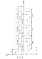
- FIG. It is explanatory drawing which shows the example of the characteristic table corresponding to the characteristic information. It is explanatory drawing which shows the example of the shift processing by shifting the control cycle. It is explanatory drawing which shows the example of the shift process by reducing the duty ratio. It is explanatory drawing which shows another example of the shift processing by shifting the control cycle. It is explanatory drawing which shows another example of the shift process by reducing the duty ratio.
- FIG. It is a block diagram which shows the other hardware configuration of the main part of the control device which concerns on Embodiment 1.
- FIG. It is a block diagram which shows the other hardware configuration of the main part of the control device which concerns on Embodiment 1.
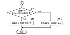
- FIG. It is a flowchart which shows the operation in the failure detection mode of the control device which concerns on Embodiment 1.
- FIG. It is a flowchart which shows the operation in the failure detection mode of the control device which concerns on Embodiment 1.
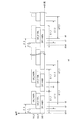
- FIG. It is explanatory drawing which shows the main part of the headlight including the other control device which concerns on Embodiment 1.
- FIG. It is explanatory drawing which shows another example of the shift processing by shifting the control cycle. It is explanatory drawing which shows another example of the shift process by reducing the duty ratio.
- FIG. 1 is an explanatory diagram showing a main part of a headlight including a control device according to the first embodiment. A headlight including the control device according to the first embodiment will be described with reference to FIG.
- the headlight 100 is provided on a vehicle (not shown).
- the light source of the headlight 100 is composed of the LED group 1.
- the LED group 1 is divided into a plurality of segments SG.
- Each segment SG comprises one LED 2 or a plurality of LEDs 2 connected in series with each other.
- the LED group 1 is divided into three segments SG_1, SG_2, and SG_3 will be mainly described.
- Segment SG_1 includes, for example, eight LEDs 2 connected in series with each other.
- Segment SG_2 includes, for example, three LEDs 2 connected in series with each other.
- Segment SG_3 includes, for example, one LED2.
- the headlight 100 has a lighting device 200 for the LED group 1.
- the lighting device 200 includes a power supply circuit 3.
- the power supply circuit 3 is composed of, for example, a DC / DC converter.
- the power supply circuit 3 supplies a current to the LED group 1 by constant current control. That is, the power supply circuit 3 supplies a predetermined current to the LED group 1.
- the lighting device 200 includes a switch circuit group 4.
- the switch circuit group 4 includes a plurality of switch circuits 5 corresponding to a plurality of segment SGs.
- the three switch circuits 5_1, 5_2, 5_3 corresponding to the three segments SG_1, SG_2, SG_3 are included in the switch circuit group 4 will be mainly described.
- the lighting device 200 includes a drive circuit 6.
- the drive circuit 6 drives one or more selected switch circuits 5 among the plurality of switch circuits 5 by PWM (Pulse Width Modulation) control. That is, the drive circuit 6 can drive a plurality of switch circuits 5 independently of each other. In other words, the drive circuit 6 can individually drive a plurality of switch circuits 5.
- PWM Pulse Width Modulation
- each switch circuit 5 When the state of each switch circuit 5 is on, the corresponding segment SG is bypassed, so that the above-mentioned predetermined current does not flow through the corresponding segment SG. As a result, the state of the corresponding segment SG is turned off. On the other hand, when the state of each switch circuit 5 is in the off state, the corresponding segment SG is not bypassed, so that the current defined above flows through the corresponding segment SG. As a result, the state of the corresponding segment SG becomes the lit state.
- one or more segment SGs corresponding to the light distribution for the low beam are included in the LED group 1.
- Light distribution for a low beam is realized by lighting the one or more segment SGs.
- one or more segment SGs corresponding to the light distribution for the high beam are included in the LED group 1.
- Light distribution for high beams is realized by lighting the one or more segment SGs.
- the lighting device 200 includes a control device 300.
- the control device 300 can communicate with the electronic control unit (hereinafter referred to as "ECU") 400.
- the ECU 400 is provided inside the vehicle and outside the headlight 100.
- the ECU 400 is a higher-level ECU with respect to the control device 300.
- the ECU 400 transmits the lighting instruction signal S1 for the headlight 100 to the control device 300.
- the control device 300 receives the transmitted lighting instruction signal S1.
- the lighting instruction signal S1 is, for example, a signal instructing the lighting of the headlight 100 by one selected type of light distribution among the plurality of types of light distribution.
- the lighting instruction signal S1 is, for example, a signal instructing the lighting of one or more selected segment SGs among the plurality of segment SGs.
- the control device 300 outputs a control signal (hereinafter referred to as "first control signal") S2 for realizing the constant current control to the power supply circuit 3 according to the content of the lighting instruction signal S1. That is, the control device 300 outputs the first control signal S2 for realizing the constant current control to the power supply circuit 3 according to the number of LEDs 2 to be lit by the light distribution indicated by the lighting instruction signal S1. .. In other words, the control device 300 controls the power supply circuit 3 by outputting the first control signal S2 to the power supply circuit 3.
- first control signal a control signal
- the control device 300 outputs a control signal (hereinafter referred to as "second control signal") S3 for realizing the above PWM control to the drive circuit 6 according to the content of the lighting instruction signal S1. That is, the control device 300 outputs the second control signal S3 for realizing the PWM control to the drive circuit 6 according to the segment SG to be lit by the light distribution indicated by the lighting instruction signal S1. In other words, the control device 300 controls the drive circuit 6 by outputting the second control signal S3 to the drive circuit 6.
- second control signal a control signal for realizing the above PWM control to the drive circuit 6 according to the content of the lighting instruction signal S1. That is, the control device 300 outputs the second control signal S3 for realizing the PWM control to the drive circuit 6 according to the segment SG to be lit by the light distribution indicated by the lighting instruction signal S1. In other words, the control device 300 controls the drive circuit 6 by outputting the second control signal S3 to the drive circuit 6.
- the LED group 1 is lit according to the content of the lighting instruction signal S1. That is, the headlight 100 is turned on by the light distribution instructed by the ECU 400.
- control device 300 has an operation mode (hereinafter referred to as "normal lighting mode") for executing control for lighting the headlight 100 (hereinafter referred to as “lighting control”) in response to an instruction from the ECU 400. ing.
- normal lighting mode an operation mode for executing control for lighting the headlight 100
- lighting control executing control for lighting the headlight 100
- Various known techniques can be used for controlling the power supply circuit 3 and the drive circuit 6 by the control device 300 in the normal lighting mode. Detailed description of these techniques will be omitted.
- control device 300 has an operation mode (hereinafter referred to as "failure detection mode") for detecting a failure in each segment SG.
- failure detection mode an operation mode for detecting a failure in each segment SG.
- the failure detection mode will be described with reference to FIGS. 1 to 7.
- the lighting device 200 includes a voltage detector 7.
- the control device 300 includes a voltage estimation unit 11, a shift processing unit 12, a voltage detection unit 13, and a failure detection unit 14.
- the voltage detector 7 continuously detects the output voltage V1 of the power supply circuit 3.
- the voltage estimation unit 11 executes a process of calculating a voltage estimate value (hereinafter referred to as "voltage estimate value”) V2 corresponding to each segment SG (hereinafter referred to as “voltage estimation process”).
- the voltage estimate V2 is calculated based on information indicating the voltage characteristics of the individual segments SG (hereinafter referred to as “characteristic information").
- the characteristic information is stored in advance in the voltage estimation unit 11, for example.
- FIG. 3 shows an example of a characteristic table corresponding to the characteristic information.
- the shift processing unit 12 executes a process of shifting the current supply timing for the LED group 1 by the power supply circuit 3 with a different shift amount ⁇ for each segment SG (hereinafter referred to as “shift process”).
- the shift process is realized by shifting the control cycle ⁇ T in the PWM control by a shift amount ⁇ different for each segment SG.
- the shift process is realized by temporarily reducing the duty ratio DR in the PWM control by a reduction amount ⁇ different for each segment SG. That is, the second control signal S3 is used for the shift process.
- the shift process is the timing at which the headlight 100 starts lighting (hereinafter sometimes referred to as “first timing") or the timing at which the content of the lighting instruction to the headlight 100 changes (hereinafter referred to as “second timing”). Is executed at at least one of the timings. That is, the second timing is the timing at which the content of the lighting instruction signal S1 changes while the headlight 100 is lit. In other words, the second timing is the timing at which the light distribution instructed by the ECU 400 changes while the headlight 100 is lit.
- the voltage detection unit 13 sequentially calculates the voltage detection value (hereinafter referred to as “voltage detection value”) V3 corresponding to each segment SG according to the shift process (hereinafter referred to as “voltage detection process”). It is what you do.
- the voltage detection value V3 is calculated using the output voltage V1 detected by the voltage detector 7.
- the failure detection unit 14 executes a process of determining the presence or absence of a failure in each segment SG (hereinafter referred to as “failure detection process”) by comparing each voltage detection value V3 with the corresponding voltage estimation value V2. Is. As a result, a failure in each segment SG is detected.
- the control device 300 When it is determined that the segment SG has a failure, the control device 300 stores information indicating the segment SG (hereinafter referred to as “failure segment information"). That is, the failure segment information is information indicating the segment SG during the failure.
- the control device 300 transmits a signal (hereinafter referred to as “failure notification signal”) S4 corresponding to the failure segment information to the ECU 400.
- the ECU 400 receives the transmitted failure notification signal S4.
- the ECU 400 transmits, for example, a lighting instruction signal S1 instructing the headlight 100 to be turned off to the control device 300.
- a lighting instruction signal S1 is transmitted, for example, when all the segment SGs are out of order.
- the ECU 400 transmits, for example, a lighting instruction signal S1 instructing the turning off of the failed segment SG to the control device 300.
- Such a lighting instruction signal S1 is transmitted, for example, when only a part of the segment SG is out of order.
- the ECU 400 executes a control for notifying the driver of the vehicle that, for example, the light distribution corresponding to the failed segment SG cannot be realized due to the failure of the headlight 100.
- the duty ratio DR_1 corresponding to the segment SG_1 is set to 100%
- the duty ratio DR_2 corresponding to the segment SG_2 is set to 100%
- the duty ratio DR_1 corresponding to the segment SG_1 is set to 100%
- the duty ratio DR_3 is set to 100%.
- the control cycle ⁇ T is shifted by a shift amount ⁇ different for each segment SG.
- each of ⁇ T_1, ⁇ T_2, and ⁇ T_3 corresponds to one period of PWM.
- the voltage estimation unit 11 calculates the voltage estimation value V2_1 corresponding to the segment SG_1, the voltage estimation value V2_2 corresponding to the segment SG_2, and the voltage estimation value V2_3 corresponding to the segment SG_3 based on the characteristic information.
- Time t0 corresponds to the first timing or the second timing.
- the voltage detection unit 13 calculates the voltage detection value V3_1 corresponding to the segment SG_1 by using the output voltage V1_1 detected by the voltage detector 7 at the time t1. That is, the voltage detection value V3_1 is calculated by the following equation (1).
- V3_1 V1_1 (1)
- the voltage detection unit 13 corresponds to the segment SG_2 by using the output voltage V1_1 detected by the voltage detector 7 at the time t1 and the output voltage V1_2 detected by the voltage detector 7 at the time t2. Calculate the voltage detection value V3_2. That is, the voltage detection value V3_2 is calculated by the following equation (2).
- V3_2 V1-2-V1-1 (2)
- the voltage detection unit 13 corresponds to the segment SG_3 by using the output voltage V1_2 detected by the voltage detector 7 at the time t2 and the output voltage V1_3 detected by the voltage detector 7 at the time t3.
- V3_3 V1_3-V1-2 (3)
- the voltage detection value V3_1, the voltage detection value V3_2, and the voltage detection value V3_3 are sequentially calculated.
- the failure detection unit 14 calculates the difference value ⁇ V_1 between the calculated voltage detection value V3_1 and the calculated voltage estimation value V2_1.
- the failure detection unit 14 determines whether or not the calculated difference value ⁇ V_1 is within a predetermined range (hereinafter referred to as “reference range”) Vth. When the calculated difference value ⁇ V_1 is within the reference range Vth, the failure detection unit 14 determines that there is no failure in the segment SG_1. If not, the failure detection unit 14 determines that there is a failure in the segment SG_1.
- the failure detection unit 14 calculates the difference value ⁇ V_2 between the calculated voltage detection value V3_2 and the calculated voltage estimation value V2_2. The failure detection unit 14 determines whether or not the calculated difference value ⁇ V_2 is within the reference range Vth. When the calculated difference value ⁇ V_2 is a value within the reference range Vth, the failure detection unit 14 determines that there is no failure in the segment SG_2. If not, the failure detection unit 14 determines that there is a failure in the segment SG_2.
- the failure detection unit 14 calculates the difference value ⁇ V_3 between the calculated voltage detection value V3_3 and the calculated voltage estimation value V2_3. The failure detection unit 14 determines whether or not the calculated difference value ⁇ V_3 is within the reference range Vth. When the calculated difference value ⁇ V_3 is a value within the reference range Vth, the failure detection unit 14 determines that there is no failure in the segment SG_3. If not, the failure detection unit 14 determines that there is a failure in the segment SG_3.
- the duty ratio DR_1 is set to 100%
- the duty ratio DR_2 is set to 100%
- the duty ratio DR_3 is set to 100%.
- the shift process in the second specific example temporarily reduces the duty ratio DR by a reduction amount ⁇ that differs for each segment SG.
- ⁇ T corresponds to one PWM cycle.
- the voltage estimation process in the second specific example is the same as the voltage estimation process in the first specific example. Therefore, the description will be omitted again.
- the duty ratio DR_2 is temporarily lowered to a value (for example, 80%) lower than the above-set value (that is, 100%). Further, the duty ratio DR_3 is temporarily lowered to a value lower than the set value (that is, 100%) (for example, 60%).
- the state of the switch circuit 5_1 is in the off state, and the state of the switch circuits 5_2, 5_3 is in the on state. Further, at time t2, the state of the switch circuits 5_1 and 5_2 is in the off state, and the state of the switch circuit 5_3 is in the on state. Further, at time t3, the state of the switch circuits 5_1, 5_2, 5_3 is off.
- the voltage detection unit 13 executes the same voltage detection process as the voltage detection process in the first specific example.
- the voltage detection value V3_1, the voltage detection value V3_2, and the voltage detection value V3_3 are sequentially calculated.
- the failure detection process in the second specific example is the same as the failure detection process in the first specific example. Therefore, the description will be omitted again.
- the duty ratio DR_1 is set to 80%
- the duty ratio DR_2 is set to 70%
- the duty ratio DR_3 is set to 60%.
- the control cycle ⁇ T is shifted by a shift amount ⁇ different for each segment SG.
- each of ⁇ T_1, ⁇ T_2, and ⁇ T_3 corresponds to one period of PWM.
- the voltage estimation process in the third specific example is the same as the voltage estimation process in the first specific example. Therefore, the description will be omitted again.
- the state of the switch circuit 5_1 is in the off state, and the state of the switch circuits 5_2, 5_3 is in the on state. Further, at time t2, the state of the switch circuits 5_1 and 5_2 is in the off state, and the state of the switch circuit 5_3 is in the on state. Further, at time t3, the state of the switch circuits 5_1, 5_2, 5_3 is off.
- the voltage detection unit 13 executes the same voltage detection process as the voltage detection process in the first specific example.
- the voltage detection value V3_1, the voltage detection value V3_2, and the voltage detection value V3_3 are sequentially calculated.
- the failure detection process in the third specific example is the same as the failure detection process in the first specific example. Therefore, the description will be omitted again.
- the duty ratio DR_1 is set to 80%
- the duty ratio DR_2 is set to 70%
- the duty ratio DR_3 is set to 60%.
- the shift process in the fourth specific example temporarily reduces the duty ratio DR by a reduction amount ⁇ that differs for each segment SG.
- ⁇ T corresponds to one PWM cycle.
- the voltage estimation process in the fourth specific example is the same as the voltage estimation process in the first specific example. Therefore, the description will be omitted again.
- the duty ratio DR_2 is temporarily lowered to a value (for example, 50%) lower than the above-set value (that is, 70%). Further, the duty ratio DR_3 is temporarily lowered to a value lower than the set value (that is, 60%) (for example, 20%).
- the state of the switch circuit 5_1 is in the off state, and the state of the switch circuits 5_2, 5_3 is in the on state. Further, at time t2, the state of the switch circuits 5_1 and 5_2 is in the off state, and the state of the switch circuit 5_3 is in the on state. Further, at time t3, the state of the switch circuits 5_1, 5_2, 5_3 is off.
- the voltage detection unit 13 executes the same voltage detection process as the voltage detection process in the first specific example.
- the voltage detection value V3_1, the voltage detection value V3_2, and the voltage detection value V3_3 are sequentially calculated.
- the failure detection process in the fourth specific example is the same as the failure detection process in the first specific example. Therefore, the description will be omitted again.
- the duty ratios DR_2 and DR_3 are temporarily lowered by executing the shift process.
- the brightness of the headlight 100 is temporarily reduced because some of the segments SG_1, SG_2, and SG_3 to be lit are temporarily not lit.
- each of the shift amounts ⁇ _1, ⁇ _2, and ⁇ _3 is set to a sufficiently small value. Thereby, it is possible to prevent such a decrease in brightness from being perceived by humans.
- a plurality of functions including the function of the voltage estimation unit 11, the function of the shift processing unit 12, the function of the voltage detection unit 13 and the function of the failure detection unit 14) of the control device 300 are simply “plurality”. There are “individual functions”. In addition, the reference numeral “F” may be used for such a plurality of functions.
- the control device 300 has a processor 21 and a memory 22. Programs corresponding to a plurality of functions F are stored in the memory 22.
- the processor 21 reads and executes the program stored in the memory 22. As a result, a plurality of functions F are realized.
- the control device 300 has a processing circuit 23.
- the processing circuit 23 executes processing corresponding to a plurality of functions F. As a result, a plurality of functions F are realized.
- the control device 300 includes a processor 21, a memory 22, and a processing circuit 23.
- a program corresponding to a part of the plurality of functions F is stored in the memory 22.
- the processor 21 reads and executes the program stored in the memory 22. As a result, some of these functions are realized.
- the processing circuit 23 executes processing corresponding to the remaining functions of the plurality of functions F. As a result, such a residual function is realized.
- the processor 21 is composed of one or more processors.
- processors for example, a CPU (Central Processing Unit), a GPU (Graphics Processing Unit), a microprocessor, a microprocessor, or a DSP (Digital Signal Processor) is used.
- CPU Central Processing Unit
- GPU Graphics Processing Unit
- microprocessor a microprocessor
- DSP Digital Signal Processor
- the memory 22 is composed of one or more non-volatile memories.
- the memory 22 is composed of one or more non-volatile memories and one or more volatile memories. That is, the memory 22 is composed of one or more memories.
- the individual memory uses, for example, a semiconductor memory or a magnetic disk. More specifically, each volatile memory uses, for example, a RAM (Random Access Memory).
- the individual non-volatile memory is, for example, a ROM (Read Only Memory), a flash memory, an EPROM (Erasable Programmable Read Only Memory), an EEPROM (Electrically Erasable Programmory) drive, or a drive solid state drive O. Is.
- the processing circuit 23 is composed of one or more digital circuits. Alternatively, the processing circuit 23 is composed of one or more digital circuits and one or more analog circuits. That is, the processing circuit 23 is composed of one or more processing circuits.
- the individual processing circuits are, for example, ASIC (Application Special Integrated Circuit), PLD (Programmable Logic Device), FPGA (Field Programmable Gate Array), FPGA (Field Program Is.
- the processor 21 when the processor 21 is composed of a plurality of processors, the correspondence between the plurality of functions F and the plurality of processors is arbitrary. That is, each of the plurality of processors may read and execute a program corresponding to one or more corresponding functions among the plurality of functions F.
- the processor 21 may include a dedicated processor corresponding to each function F.
- each of the plurality of memories may store a program corresponding to one or more corresponding functions among the plurality of functions F.
- the memory 22 may include a dedicated memory corresponding to each function F.
- the processing circuit 23 when the processing circuit 23 is composed of a plurality of processing circuits, the correspondence between the plurality of functions F and the plurality of processing circuits is arbitrary. That is, each of the plurality of processing circuits may execute the processing corresponding to one or more corresponding functions among the plurality of functions F.
- the processing circuit 23 may include a dedicated processing circuit corresponding to each function F.
- the operation of the control device 300 will be described focusing on the operation in the failure detection mode. That is, the process shown in FIG. 11 is started at the first timing or the second timing.
- step ST2 When the lighting instruction signal S1 indicates that two or more segment SGs are lit (step ST1 “YES”), the shift processing unit 12 starts the shift process (step ST2). As a result, as described with reference to FIGS. 4 to 7, the two or more segment SGs start lighting in sequence. At this time, the following steps ST3 to ST5 are executed, and the following steps ST6 are appropriately executed.
- the voltage estimation unit 11 calculates the voltage estimation value V2 (step ST3), and the voltage detection unit 13 calculates the voltage detection value V3.
- the failure detection unit 14 determines the presence or absence of a failure (step ST5). When it is determined that there is a failure (step ST5 “NO”), the failure segment information is stored (step ST6).
- step ST7 “NO”) voltage estimation processing, voltage detection processing, and failure detection processing are executed for all segment SGs among the two or more segment SGs.
- step ST7 “YES”) When the failure detection process for all the segment SGs is completed (step ST7 “YES”) and the failure segment information indicating at least one segment SG is stored (step ST8 “YES”), the control device 300 Transmits the failure notification signal S4 to the ECU 400 (step ST9). If not (step ST8 “NO”), the control device 300 shifts from the failure detection mode to the normal lighting mode (step ST10).
- step ST1 “NO”) If the lighting instruction signal S1 indicates that only one segment SG is lit (step ST1 “NO”), the shift process is not required. Therefore, the process of step ST2 is skipped. As a result, the one segment SG starts lighting.
- the voltage estimation process (step ST3), the current estimation process (step ST4), and the failure detection process (step ST5) are executed only once without looping.
- the conventional control device uses a plurality of voltage detectors corresponding to a plurality of segments when calculating the voltage detection value corresponding to each segment.
- P_1, P_2, and P_3 in FIG. 1 show an example of a position corresponding to a position where a plurality of voltage detectors are provided. Since a plurality of voltage detectors are provided, there is a problem that the circuit scale of the lighting device becomes large.
- the voltage detection unit 13 can calculate the voltage detection value V3 corresponding to each segment SG by using one voltage detector 7. That is, by using the control device 300, the number of voltage detectors 7 in the lighting device 200 can be reduced. As a result, the circuit scale of the lighting device 200 can be reduced.
- control device 300 Next, a modified example of the control device 300 will be described with reference to FIG.
- the voltage characteristics of individual segment SGs have current dependence. Therefore, as shown in FIG. 12, in the lighting device 200, the current flowing through each segment SG is detected, and a value (hereinafter referred to as “current detection value”) I indicating the detected current is transmitted to the control device 300. It may be input.
- the voltage estimation unit 11 may calculate the voltage estimation value V2 based on the characteristic information including the current-voltage characteristics of the individual segments SG using the input current detection value I. As a result, the voltage estimation value V2 can be calculated more accurately. As a result, it is possible to more accurately determine the presence or absence of a failure in each segment SG.
- the temperature in the headlight 100 is detected by the temperature detector 8, and a value T indicating the detected temperature (hereinafter referred to as “temperature detection value”) T is input to the control device 300. It may be one.
- the temperature detector 8 is composed of, for example, a thermistor.
- the voltage estimation unit 11 may calculate the voltage estimation value V2 based on the characteristic information including the temperature-voltage characteristics of each segment SG by using the input temperature detection value T. As a result, the voltage estimation value V2 can be calculated more accurately. As a result, it is possible to more accurately determine the presence or absence of a failure in each segment SG.
- the control device 300 is the control device 300 of the headlight 100 having the LED group 1 including a plurality of segment SGs, and the voltage estimation value corresponding to each segment SG.
- the voltage estimation unit 11 that calculates V2
- the shift processing unit 12 that executes the shift processing that shifts the current supply timing for the LED group 1 by the power supply circuit 3 with a different shift amount ⁇ for each segment SG, and the shift processing unit 12 according to the shift processing.
- the voltage detector 13 that sequentially calculates the voltage detection value V3 corresponding to each segment SG using the voltage detector 7 that detects the output voltage V1 of the power supply circuit 3, and the voltage estimation corresponding to each voltage detection value V3.
- a failure detection unit 14 that executes a failure detection process for determining the presence or absence of a failure in each segment SG by comparing with the value V2 is provided.
- the number of voltage detectors 7 in the lighting device 200 can be reduced in detecting a failure in each segment SG.
- the circuit scale of the lighting device 200 can be reduced.
- the shift process is realized by shifting the control cycle ⁇ T corresponding to each segment SG by a shift amount ⁇ different for each segment SG.
- the shift process can be realized without lowering the duty ratio DR.
- shift processing can be realized while maintaining the duty ratio DR corresponding to all segment SGs at 100%.
- the shift process is realized by reducing the duty ratio DR corresponding to each segment SG by a reduction amount ⁇ different for each segment SG.
- the individual reduction amount ⁇ is set to a sufficiently small value.
- the shift process and the failure detection process are executed. As a result, it is possible to detect a failure in each segment SG at the first timing.
- the shift process and the failure detection process are executed. As a result, it is possible to detect a failure in each segment SG at the second timing.
- the voltage estimation unit 11 calculates the voltage estimation value V2 using the current detection value I corresponding to each segment. As a result, the voltage estimation value V2 can be calculated with high accuracy. As a result, it is possible to accurately determine the presence or absence of a failure in each segment SG.
- the voltage estimation unit 11 calculates the voltage estimation value V2 using the temperature detection value T. As a result, the voltage estimation value V2 can be calculated with high accuracy. As a result, it is possible to accurately determine the presence or absence of a failure in each segment SG.
- Embodiment 2 The timing at which the shift process, the failure detection process, and the like are executed is not limited to the first timing and the second timing. In the second embodiment, a modification of the control device 300 in which the shift process, the failure detection process, and the like are executed at other timings will be described.
- the following timings (hereinafter referred to as "third timing") may be used. Yes.) May be executed.
- the shift process, the failure detection process, and the like may be executed at at least one of the first timing, the second timing, and the third timing.
- the third timing is the timing at which the output voltage V1 detected by the voltage detector 7 changes even though the content of the lighting instruction to the headlight 100 by the ECU 400 (that is, the content of the lighting instruction signal S1) has not changed.
- the control device 300 has a function of shifting from the normal lighting mode to the failure detection mode at the third timing. As a result, shift processing, failure detection processing, and the like are executed.
- the time t0 corresponds to the first timing or the second timing.
- the same voltage estimation processing, shift processing, voltage detection processing, and failure detection processing as those described with reference to FIG. 4 in the first embodiment are executed. It is determined by the failure detection process that there is no failure in any of the segment SGs, and the control device 300 shifts from the failure detection mode to the normal lighting mode. After that, the control device 300 monitors the output voltage V1 detected by the voltage detector 7.
- the voltage estimation unit 11 calculates the voltage estimation value V2_1 corresponding to the segment SG_1, the voltage estimation value V2_2 corresponding to the segment SG_2, and the voltage estimation value V2_3 corresponding to the segment SG_3 based on the characteristic information.
- the voltage detection unit 13 calculates the voltage detection value V3_1 corresponding to the segment SG_1 by using the output voltage V1_1 detected by the voltage detector 7 at the time t6.
- the voltage detection value V3_1 is calculated by the above equation (1).
- the voltage detection unit 13 corresponds to the segment SG_2 by using the output voltage V1_1 detected by the voltage detector 7 at the time t6 and the output voltage V1_2 detected by the voltage detector 7 at the time t7. Calculate the voltage detection value V3_2.
- the voltage detection value V3_2 is calculated by the above equation (2).
- the voltage detection unit 13 corresponds to the segment SG_3 by using the output voltage V1_2 detected by the voltage detector 7 at the time t7 and the output voltage V1_3 detected by the voltage detector 7 at the time t8. Calculate the voltage detection value V3_3.
- the voltage detection value V3_3 is calculated by the above equation (3).
- the voltage detection value V3_1, the voltage detection value V3_2, and the voltage detection value V3_3 are sequentially calculated.
- the failure detection unit 14 executes the failure detection process.
- the failure detection process it is determined that there is no failure in the segment SG_1 because the difference value ⁇ V_1 is within the reference range Vth. Further, since the difference value ⁇ V_2 is a value within the reference range Vth, it is determined that there is no failure in the segment SG_2. On the other hand, when the difference value ⁇ V_3 is a value outside the reference range Vth, it is determined that there is a failure in the segment SG_3.
- the time t0 corresponds to the first timing or the second timing.
- the same voltage estimation processing, shift processing, voltage detection processing, and failure detection processing as those described with reference to FIG. 5 in the first embodiment are executed. It is determined by the failure detection process that there is no failure in any of the segment SGs, and the control device 300 shifts from the failure detection mode to the normal lighting mode. After that, the control device 300 monitors the output voltage V1 detected by the voltage detector 7.
- the voltage estimation process in the sixth specific example is the same as the voltage estimation process in the fifth specific example. Therefore, the description will be omitted again.
- the duty ratio DR_2 is temporarily lowered to a value lower than the set value (that is, 100%) (for example, 80%).
- the duty ratio DR_3 is temporarily lowered to a value lower than the set value (that is, 100%) (for example, 60%).
- the state of the switch circuit 5_1 is in the off state, and the state of the switch circuits 5_2, 5_3 is in the on state.
- the state of the switch circuits 5_1 and 5_2 is in the off state, and the state of the switch circuit 5_3 is in the on state.
- the state of the switch circuits 5_1, 5_2, 5_3 is off.
- the voltage detection unit 13 executes the same voltage detection process as the voltage detection process in the fifth specific example.
- the voltage detection value V3_1, the voltage detection value V3_2, and the voltage detection value V3_3 are sequentially calculated.
- the failure detection process in the sixth specific example is the same as the failure detection process in the fifth specific example. Therefore, the description will be omitted again.
- the time t0 corresponds to the first timing or the second timing.
- the same voltage estimation processing, shift processing, voltage detection processing, and failure detection processing as those described with reference to FIG. 6 in the first embodiment are executed. It is determined by the failure detection process that there is no failure in any of the segment SGs, and the control device 300 shifts from the failure detection mode to the normal lighting mode. After that, the control device 300 monitors the output voltage V1 detected by the voltage detector 7.
- the voltage estimation process in the 7th specific example is the same as the voltage estimation process in the 5th specific example. Therefore, the description will be omitted again.
- the state of the switch circuit 5_1 is in the off state, and the state of the switch circuits 5_2, 5_3 is in the on state.
- the state of the switch circuits 5_1 and 5_2 is in the off state, and the state of the switch circuit 5_3 is in the on state.
- the state of the switch circuits 5_1, 5_2, 5_3 is off.
- the voltage detection unit 13 executes the same voltage detection process as the voltage detection process in the fifth specific example.
- the voltage detection value V3_1, the voltage detection value V3_2, and the voltage detection value V3_3 are sequentially calculated.
- the failure detection process in the 7th specific example is the same as the failure detection process in the 5th specific example. Therefore, the description will be omitted again.
- the time t0 corresponds to the first timing or the second timing.
- the same voltage estimation processing, shift processing, voltage detection processing, and failure detection processing as those described with reference to FIG. 7 in the first embodiment are executed. It is determined by the failure detection process that there is no failure in any of the segment SGs, and the control device 300 shifts from the failure detection mode to the normal lighting mode. After that, the control device 300 monitors the output voltage V1 detected by the voltage detector 7.
- the voltage estimation process in the 8th specific example is the same as the voltage estimation process in the 5th specific example. Therefore, the description will be omitted again.
- the duty ratio DR_2 is temporarily lowered to a value lower than the set value (that is, 70%) (for example, 50%).
- the duty ratio DR_3 is temporarily lowered to a value lower than the set value (that is, 60%) (for example, 20%).
- the state of the switch circuit 5_1 is in the off state, and the state of the switch circuits 5_2, 5_3 is in the on state.
- the state of the switch circuits 5_1 and 5_2 is in the off state, and the state of the switch circuit 5_3 is in the on state.
- the state of the switch circuits 5_1, 5_2, 5_3 is off.
- the voltage detection unit 13 executes the same voltage detection process as the voltage detection process in the fifth specific example.
- the voltage detection value V3_1, the voltage detection value V3_2, and the voltage detection value V3_3 are sequentially calculated.
- the failure detection process in the eighth specific example is the same as the failure detection process in the fifth specific example. Therefore, the description will be omitted again.
- the non-failed segments SG_1 and SG_2 among the segments SG_1, SG_2, and SG_3 that should be lit by executing the shift process at the third timing Some segments SG_2 are temporarily turned off. As a result, the brightness of the headlight 100 is temporarily reduced.
- each of the shift amounts ⁇ _1, ⁇ _2, and ⁇ _3 is set to a sufficiently small value. Thereby, it is possible to prevent such a decrease in brightness from being perceived by humans.
- the operation of the control device 300 will be described focusing on the operation in the normal lighting mode. That is, the process shown in FIG. 17 is started when the control device 300 shifts from the failure detection mode to the normal lighting mode.
- control device 300 starts monitoring the output voltage V1 detected by the voltage detector 7 (step ST21). Further, the control device 300 starts lighting control according to the content of the lighting instruction by the ECU 400 (step ST22).
- step ST23 “YES” When the content of the lighting instruction changes (step ST23 “YES”), the process of the control device 300 returns to step ST22.
- step ST24 “YES” when the content of the lighting instruction has not changed (step ST23 “NO”), the control device 300 shifts from the normal lighting mode to the failure detection mode. (Step ST25). As a result, the process shown in FIG. 11 is started.
- the control device 300 when the content of the lighting instruction to the headlight 100 has not changed and the output voltage V1 of the power supply circuit 3 has changed, the shift process and the failure have occurred.
- the detection process is executed. As a result, it is possible to detect a failure in each segment SG at the third timing.
- the corresponding segment SG is temporarily turned off.
- the individual shift amounts ⁇ are set to a sufficiently small value, it is possible to avoid a decrease in the brightness of the headlight 100 being perceived by humans.
- the control device according to the present disclosure can be used for headlights.
Landscapes
- Engineering & Computer Science (AREA)
- Mechanical Engineering (AREA)
- Automatic Tape Cassette Changers (AREA)
- Automatic Disk Changers (AREA)
- Lighting Device Outwards From Vehicle And Optical Signal (AREA)
Priority Applications (2)
| Application Number | Priority Date | Filing Date | Title |
|---|---|---|---|
| JP2022509799A JP7109700B2 (ja) | 2020-03-24 | 2020-03-24 | 制御装置 |
| PCT/JP2020/012815 WO2021191992A1 (ja) | 2020-03-24 | 2020-03-24 | 制御装置 |
Applications Claiming Priority (1)
| Application Number | Priority Date | Filing Date | Title |
|---|---|---|---|
| PCT/JP2020/012815 WO2021191992A1 (ja) | 2020-03-24 | 2020-03-24 | 制御装置 |
Publications (1)
| Publication Number | Publication Date |
|---|---|
| WO2021191992A1 true WO2021191992A1 (ja) | 2021-09-30 |
Family
ID=77892468
Family Applications (1)
| Application Number | Title | Priority Date | Filing Date |
|---|---|---|---|
| PCT/JP2020/012815 Ceased WO2021191992A1 (ja) | 2020-03-24 | 2020-03-24 | 制御装置 |
Country Status (2)
| Country | Link |
|---|---|
| JP (1) | JP7109700B2 (https=) |
| WO (1) | WO2021191992A1 (https=) |
Citations (3)
| Publication number | Priority date | Publication date | Assignee | Title |
|---|---|---|---|---|
| JP2006210272A (ja) * | 2005-01-31 | 2006-08-10 | Matsushita Electric Works Ltd | Led駆動装置、及びそれを用いた照明装置 |
| JP2009134933A (ja) * | 2007-11-29 | 2009-06-18 | Mitsubishi Electric Corp | Led点灯装置および車両用前照灯 |
| JP2016201337A (ja) * | 2015-04-14 | 2016-12-01 | 株式会社デンソー | 発光装置 |
-
2020
- 2020-03-24 JP JP2022509799A patent/JP7109700B2/ja active Active
- 2020-03-24 WO PCT/JP2020/012815 patent/WO2021191992A1/ja not_active Ceased
Patent Citations (3)
| Publication number | Priority date | Publication date | Assignee | Title |
|---|---|---|---|---|
| JP2006210272A (ja) * | 2005-01-31 | 2006-08-10 | Matsushita Electric Works Ltd | Led駆動装置、及びそれを用いた照明装置 |
| JP2009134933A (ja) * | 2007-11-29 | 2009-06-18 | Mitsubishi Electric Corp | Led点灯装置および車両用前照灯 |
| JP2016201337A (ja) * | 2015-04-14 | 2016-12-01 | 株式会社デンソー | 発光装置 |
Also Published As
| Publication number | Publication date |
|---|---|
| JP7109700B2 (ja) | 2022-07-29 |
| JPWO2021191992A1 (https=) | 2021-09-30 |
Similar Documents
| Publication | Publication Date | Title |
|---|---|---|
| US20240008151A1 (en) | Systems and methods for controlling currents flowing through light emitting diodes | |
| US9320107B2 (en) | Vehicular lamp | |
| US8222839B2 (en) | Dimming control system for vehicular lamp | |
| JP6495926B2 (ja) | 照明装置 | |
| TWI426816B (zh) | 發光二極體的驅動電源控制電路與驅動電源控制方法 | |
| JP2007126041A (ja) | 車両用灯具の点灯制御装置 | |
| JP6783790B2 (ja) | 点灯回路、車両用灯具 | |
| JP2007112237A (ja) | 車両用灯具の点灯制御装置 | |
| KR20070009645A (ko) | 복수의 부하를 구동시키기 위한 시스템 및 방법 | |
| JP2008091311A (ja) | Led駆動装置 | |
| JP2009006979A (ja) | 車両用灯具 | |
| US20130038210A1 (en) | Device for supplying a plurality of led units with power | |
| US20200314984A1 (en) | Vehicle front lighting apparatus and disconnection detection method | |
| JP2008522566A (ja) | 負荷開放検出機能を有する電力スイッチング装置 | |
| US20120161822A1 (en) | Electrical load driving apparatus | |
| US7005978B2 (en) | Vehicle direction indication device with flash rate that does not appear to change when battery voltage varies | |
| US6583570B1 (en) | Discharge lamp device for vehicle | |
| EP4358648A1 (en) | Lighting control device, lighting control method, and lighting device | |
| JP7109700B2 (ja) | 制御装置 | |
| JP2007290450A (ja) | 照明装置 | |
| JP2007080540A (ja) | 照明システム | |
| JP5545082B2 (ja) | ランプ駆動装置 | |
| JP7317238B2 (ja) | 回路システム | |
| WO2023106199A1 (ja) | 点灯回路、及び車両用灯具 | |
| JP4933283B2 (ja) | 車両用メータ調光装置 |
Legal Events
| Date | Code | Title | Description |
|---|---|---|---|
| 121 | Ep: the epo has been informed by wipo that ep was designated in this application |
Ref document number: 20927989 Country of ref document: EP Kind code of ref document: A1 |
|
| ENP | Entry into the national phase |
Ref document number: 2022509799 Country of ref document: JP Kind code of ref document: A |
|
| NENP | Non-entry into the national phase |
Ref country code: DE |
|
| 122 | Ep: pct application non-entry in european phase |
Ref document number: 20927989 Country of ref document: EP Kind code of ref document: A1 |