WO2021186596A1 - アンテナ装置 - Google Patents
アンテナ装置 Download PDFInfo
- Publication number
- WO2021186596A1 WO2021186596A1 PCT/JP2020/011863 JP2020011863W WO2021186596A1 WO 2021186596 A1 WO2021186596 A1 WO 2021186596A1 JP 2020011863 W JP2020011863 W JP 2020011863W WO 2021186596 A1 WO2021186596 A1 WO 2021186596A1
- Authority
- WO
- WIPO (PCT)
- Prior art keywords
- feeding
- antenna
- substrate
- board
- antenna device
- Prior art date
- Legal status (The legal status is an assumption and is not a legal conclusion. Google has not performed a legal analysis and makes no representation as to the accuracy of the status listed.)
- Ceased
Links
Images


Classifications
-
- H—ELECTRICITY
- H01—ELECTRIC ELEMENTS
- H01Q—ANTENNAS, i.e. RADIO AERIALS
- H01Q13/00—Waveguide horns or mouths; Slot antennas; Leaky-waveguide antennas; Equivalent structures causing radiation along the transmission path of a guided wave
- H01Q13/08—Radiating ends of two-conductor microwave transmission lines, e.g. of coaxial lines, of microstrip lines
Definitions
- This disclosure relates to an antenna device.
- the probe power supply has a space-saving power supply structure as compared with the method of power supply by electromagnetic coupling using a slot. Therefore, it is suitable for multipoint feeding of a single patch element in applications of orthogonal dipolarization, circular polarization, or low cross polarization of signals.
- the antenna substrate is thickened in order to widen the frequency band used in the antenna device that feeds the probe. As the antenna substrate becomes thicker, the probe becomes longer by that amount, so that the inductance component becomes larger, and there is a possibility that the inductance matching between the patch element and the feeding circuit cannot be obtained.
- Non-Patent Document 1 describes a technique of forming a conductor land at the tip of a probe and compensating for an inductance component of the probe by a capacitance component generated between the patch element and the conductor land.
- Non-Patent Document 1 it is necessary to form a through hole for electrically connecting the patch element provided on the antenna board and the feeding board. Therefore, the antenna board is stacked on the feeding board in multiple layers. is required.
- the multilayer substrate may warp. Therefore, in the conventional antenna device, when the antenna board is made thicker than the feeding board in order to widen the frequency band used, the surface of the feeding board opposite to the antenna board side has the same thickness as the antenna board. It is necessary to further provide the antenna, and there is a problem that the thickness of the entire substrate is increased.
- the present disclosure solves the above problems, and an object of the present disclosure is to obtain an antenna device capable of reducing an increase in the thickness of the entire substrate.
- the antenna device includes a flat-plate antenna substrate, one or more radiation conductors provided on the antenna substrate, and a first feeding conductor provided on a main surface of the antenna substrate opposite to the radiation conductor. And a flat plate-shaped power supply board provided with a power supply unit for feeding a signal transmitted to the antenna board side, and a through hole that electrically connects the radiation conductor and the first power supply conductor through the antenna board.
- a second feeding conductor provided on the main surface of the feeding board on the antenna board side and an intermediate board provided between the antenna board and the feeding board are provided, and the first feeding conductor and the second feeding conductor are provided. And are capacitively bonded with the intermediate substrate in between.
- the antenna board and the feeding board are capacitively coupled. Even if the through hole provided between the two is divided in the middle, the probe can be fed from the feeding board to the antenna board. Since the thickness of the antenna board and the feeding board can be multi-layered so as to be substantially symmetrical in the layer thickness direction with the intermediate board as a reference, the surface of the feeding board opposite to the side on which the antenna board is provided is provided. It is not necessary to provide a substrate having the same thickness as the antenna substrate. Thereby, in the antenna device according to the present disclosure, it is possible to reduce the increase in the thickness of the entire substrate.
- FIG. 5 is a side perspective view showing the antenna device of FIG. 4 in which a positional deviation occurs between the antenna substrate and the feeding substrate.
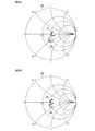
- FIG. 6A is a Smith chart diagram showing the input impedance of a single patch element in the antenna device of FIG. 1 before and after a positional shift occurs between the antenna board and the feeding board
- FIG. 6B is a Smith chart diagram of the antenna board and the feeding board.
- FIG. 10A is a Smith chart diagram showing the input impedance of a single patch element in the antenna device of FIG. 4 before and after a positional shift occurs between the antenna board and the feeding board
- FIG. 10B shows the antenna board and the feeding board.
- FIG. It is a Smith chart figure which shows the input impedance of a single patch element in the antenna device of FIG. It is a side perspective view which shows the antenna device which concerns on Embodiment 4.
- FIG. It is a top view which shows the antenna device of FIG. It is a side perspective view which shows the modification of the antenna device of FIG. It is a top view which shows the antenna device of FIG. It is a top view which shows the example of the feeding conductor of the antenna substrate in the antenna device of FIG. It is a top view which shows the example of the feeding conductor of the feeding board in the antenna device of FIG. It is a top view which shows the example of the feeding conductor of the antenna substrate in the antenna device of FIG.
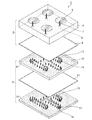
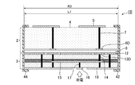
- FIG. 1 is a side perspective view showing the antenna device 1 according to the first embodiment.
- FIG. 2 is an exploded perspective view showing a substrate of each layer in the antenna device 1 of FIG.
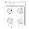
- the antenna device 1 is a 4-element array antenna having four patch elements 5, and a signal is transmitted to an antenna substrate 2 that radiates a signal radio wave into space through the patch element 5 and an antenna substrate 2.
- a power supply board 3 for supplying power is provided.
- the patch element 5 is, for example, a circular radiation conductor, and functions as a radiation element that emits radio waves.
- the antenna substrate 2 is composed of a flat plate-shaped dielectric substrate 4, and a patch element 5 is provided on the main surface of the dielectric substrate 4, and the main surface of the dielectric substrate 4 is opposite to the patch element 5.
- the circular feeding conductor 6 is a first feeding conductor provided at a position facing the patch element 5 via the dielectric substrate 4.
- the patch element 5 and the feeding conductor 6 are electrically connected by a through hole 7.
- the through hole 7 is a probe that supplies a signal to the patch element 5.
- the antenna substrate 2 is provided with a flat plate-shaped dielectric 8 which is an intermediate substrate on the main surface on the power feeding substrate 3 side.
- the power supply substrate 3 is a multilayer substrate in which a substrate 9 and a substrate 10 having substantially the same thickness are bonded by an adhesive layer 11.
- a main plate 12 and a feeding conductor 13 are provided on the main surface of the feeding board 3 on the antenna board 2 side.
- the circular feeding conductor 13 is a second feeding conductor electrically connected to the 4-distribution synthesis circuit 15 by the vertical feeding portion 14, and is provided so as not to be electrically connected to the main plate 12.
- the 4-distribution synthesis circuit 15 is composed of triplate lines.
- the power feeding unit 16 is provided on the main surface of the power feeding board 3 on the side opposite to the antenna board 2.
- the 4-distribution synthesis circuit 15 and the feeding unit 16 are electrically connected by a vertical feeding unit 17.
- the feeding conductor 6 and the feeding conductor 13 are not in physical contact with each other due to the dielectric 8.
- the signal input to the feeding unit 16 is fed to the feeding conductor 13 by propagating through the vertical feeding unit 17, the 4-distribution synthesis circuit 15 and the vertical feeding unit 14.
- the feeding conductor 6 and the feeding conductor 13 are capacitively coupled with the dielectric 8 interposed therebetween.
- the signal propagated to the feeding conductor 13 is propagated to the feeding conductor 6 and fed to the patch element 5 through the through hole 7.
- the capacitance component existing between the feeding conductor 6 and the feeding conductor 13 is proportional to the area where the feeding conductor 6 and the feeding conductor 13 face each other, but is inversely proportional to the distance between the feeding conductor 6 and the feeding conductor 13. do.
- the power feeding conductor 6 and the power feeding conductor 13 have the same area, for example.
- FIG. 3 is a circuit diagram showing an equivalent circuit when the antenna board 2 side is viewed from the feeding unit 16.
- the input impedance A of the antenna device 1 has an inductance component 101 of the through hole 7 and a capacitance component 102 between the feeding conductor 6 and the feeding conductor 13 with respect to the load 100 of the parallel resonant circuit of the patch element 5. Are connected in series.
- the inductance component and the capacitance component contained in the load 100 cancel each other out, so that only the resistance component remains. Further, the inductance component 101 connected in series with the load 100 is canceled by the capacitance component 102 connected in series. As a result, in order to widen the frequency band used by the antenna substrate 2, the dielectric substrate 4 is thickened, and even if the through hole 7 is lengthened accordingly, the antenna device 1 can achieve inductance matching. Is.
- the antenna device 1 since the feeding conductor 6 and the feeding conductor 13 are capacitively coupled, the signal from the feeding board 3 is sent to the antenna board 2 even if the vertical feeding portion 14 and the through hole 7 are separated. Powered. Therefore, the antenna device 1 can be manufactured only by manufacturing the antenna board 2 and the feeding board 3 separately and stacking the antenna board 2 on the feeding board 3. Therefore, it is not necessary to have both the antenna board 2 and the power feeding board 3 in multiple layers.
- the power feeding conductor 6 provided on the antenna board 2 and the power feeding conductor 13 provided on the power feeding board 3 are capacitively coupled with the dielectric 8 interposed therebetween. Therefore, even if the through hole 7 provided between the antenna board 2 and the feeding board 3 and the vertical feeding section 14 are separated in the middle, the probe feeding can be supplied from the feeding board 3 to the antenna board 2. Since the thickness of the antenna substrate 2 and the feeding substrate 3 can be multi-layered with reference to the dielectric 8 so as to be substantially symmetrical in the layer thickness direction, the surface of the feeding substrate 3 opposite to the antenna substrate 2 side. It is not necessary to provide a substrate having the same thickness as that of the antenna substrate 2. As a result, the antenna device 1 can reduce the increase in the thickness of the entire substrate.
- Embodiment 2 The antenna device according to the second embodiment has the same effect as that of the first embodiment, and can alleviate the influence of characteristic deterioration due to the misalignment between the multi-layered antenna substrate and the feeding substrate.
- the four corners of the stacked boards may be screwed. Since this fixing structure requires the opening diameter of the through hole to be larger than the diameter of the screw, the difference between the diameter of the screw and the opening diameter of the through hole may play a role and cause a misalignment of the stacked substrates.
- the antenna device 1 when the position shift occurs between the antenna substrate 2 and the feeding substrate 3, the facing area of the feeding conductor 6 and the feeding conductor 13 changes, so that the reflection characteristic deteriorates.
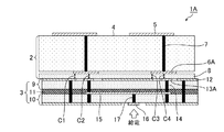
- FIG. 4 is a side perspective view showing the antenna device 1A according to the second embodiment, and the same components as those in FIG. 1 are designated by the same reference numerals and detailed description thereof will be omitted.
- the antenna device 1A is, for example, a four-element array antenna, and includes an antenna substrate 2 that radiates a signal radio wave into space through a patch element 5, and a feeding substrate 3 that feeds a signal to the antenna substrate 2.
- the feeding conductor 6A is a first feeding conductor provided at a position facing the patch element 5 via the dielectric substrate 4 of the antenna substrate 2.
- the patch element 5 and the feeding conductor 6A are electrically connected by a through hole 7.
- the feeding conductor 13A is a second feeding conductor provided on the main surface of the feeding board 3 on the antenna board 2 side.
- the circular feeding conductor 13A is provided so as not to be electrically connected to the main plate 12, and is electrically connected to the 4-distribution synthesis circuit 15 by the vertical feeding portion 14.
- the feeding conductor 6A has a larger area than the feeding conductor 13A.
- FIG. 5 is a side perspective view showing the antenna device 1A in which the position shift occurs between the antenna substrate 2 and the feeding substrate 3.
- the antenna substrate 2 and the feeding substrate 3 are misaligned to the extent that the feeding conductor 13A moves within the diameter range of the circular feeding conductor 6A.
- the amount of change in the capacitance component generated between the feeding conductor 6A and the feeding conductor 13A shown by B1 and B2 is small. Therefore, the deterioration of the reflection characteristic due to the change in the facing area between the feeding conductor 6A and the feeding conductor 13A is reduced.
- FIG. 6A is a Smith chart diagram showing the input impedance of a single patch element 5 in the antenna device 1 before and after a positional shift occurs between the antenna substrate 2 and the feeding substrate 3.
- FIG. 6B is a Smith chart diagram showing the input impedance of a single patch element 5 in the antenna device 1A before and after a positional shift occurs between the antenna substrate 2 and the feeding substrate 3.
- the charts shown in FIGS. 6A and 6B show that the closer to the center of the circle in the chart, the smaller the reflection, and the closer to the edge of the circle, the greater the reflection.
- the solid line 31 and the solid line 33 show the reflection characteristics when there is no positional deviation between the antenna substrate 2 and the feeding substrate 3.
- the broken line 32 and the broken line 34 show the reflection characteristics when a positional deviation of 0.015 ⁇ c is applied between the antenna substrate 2 and the feeding substrate 3.
- ⁇ c is the design center frequency of the antenna devices 1 and 1A.
- the double-headed arrows shown in FIGS. 6A and 6B indicate the amount of change in input impedance at the same frequency.
- the feeding conductor 13A moves within the diameter of the feeding conductor 6A.
- the feeding conductor 6 and the feeding conductor 13 have the same area, if a misalignment of 0.015 ⁇ c occurs between the antenna substrate 2 and the feeding substrate 3, the feeding conductor 6 and the feeding conductor 6 The area facing the power feeding conductor 13 changes (decreases).
- the length of the arrow shown in FIG. 6B is shorter than the length of the arrow shown in FIG. 6A due to the change in the facing area between the feeding conductor 6 and the feeding conductor 13. That is, the amount of change in the input impedance in the antenna device 1A shown in FIG. 6B is smaller than the amount of change in the input impedance in the antenna device 1 shown in FIG. 6A.
- the feeding conductor 6A is formed to have a larger area than the feeding conductor 13A.
- the antenna device 1A can reduce the influence on the input impedance, that is, the deterioration of the reflection characteristics, caused by the positional deviation between the antenna substrate 2 and the feeding substrate 3.
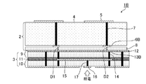
- FIG. 7 is a side perspective view showing the antenna device 1B according to the third embodiment, and the same components as those in FIG. 1 are designated by the same reference numerals, and detailed description thereof will be omitted.
- the antenna device 1B is, for example, a four-element array antenna, and includes an antenna substrate 2 that radiates a signal radio wave into space through a patch element 5, and a feeding substrate 3 that feeds a signal to the antenna substrate 2.
- the feeding conductor 6B is a first feeding conductor provided at a position facing the patch element 5 via the dielectric substrate 4 of the antenna substrate 2.
- the patch element 5 and the feeding conductor 6B are electrically connected by a through hole 7.
- the feeding conductor 13B is a second feeding conductor provided on the main surface of the feeding board 3 on the antenna board 2 side.
- the circular feeding conductor 13B is provided so as not to be electrically connected to the main plate 12, and is electrically connected to the 4-distribution synthesis circuit 15 by the vertical feeding portion 14.
- the feeding conductor 6B has a smaller area than the feeding conductor 13B.
- the antenna device 1B can be referred to as the feeding conductor 6B as long as the feeding conductor 6B moves within the diameter of the feeding conductor 13B even if the position of the antenna device 1B is displaced between the antenna substrate 2 and the feeding conductor 3. There is no change in the facing area of the feeding conductor 13B, and the deterioration of the reflection characteristics due to the change in the facing area of the feeding conductor 6B and the feeding conductor 13B is reduced.
- FIG. 8 is a side perspective view showing the antenna device 1A in which the position shift occurs between the antenna substrate 2 and the feeding substrate 3.
- the feeding conductor 6A is larger than the area of the feeding conductor 13A, when the positional deviation between the antenna substrate 2 and the feeding substrate 3 is large, as shown by arrows C2 and C4 in FIG. 8, the feeding conductor A portion where the feeding conductor 6A and the feeding conductor 13A face each other and a portion where the feeding conductor 6A and the main plate 12 of the feeding substrate 3 face each other are generated as shown by arrows C1 and C3.
- FIG. 9 is a side perspective view showing the antenna device 1B in which the position shift occurs between the antenna substrate 2 and the feeding substrate 3.
- the feeding conductor 13B is larger than the area of the feeding conductor 6B, and there is no main plate around the feeding conductor 6B on the main surface of the dielectric substrate 4.
- the antenna device 1A is displaced so that the feeding conductor 6A faces the main plate 12, the feeding conductor 6B does not face a portion other than the feeding conductor 13B.
- FIG. 10A is a Smith chart diagram showing the input impedance of a single patch element 5 in the antenna device 1A before and after a positional shift occurs between the antenna substrate 2 and the feeding substrate 3.
- FIG. 10B is a Smith chart diagram showing the input impedance of a single patch element 5 in the antenna device 1B before and after a positional shift occurs between the antenna substrate 2 and the feeding substrate 3.
- the charts shown in FIGS. 10A and 10B show that the closer to the center of the circle in the chart, the smaller the reflection, and the closer to the edge of the circle, the larger the reflection.
- the solid line 33 and the solid line 36 show the reflection characteristics when there is no positional deviation between the antenna substrate 2 and the feeding substrate 3.
- the broken line 35 and the broken line 37 show the reflection characteristics when a positional deviation of 0.02 ⁇ c is applied between the antenna substrate 2 and the feeding substrate 3.
- ⁇ c is the design center frequency of the antenna devices 1A and 1B.
- the double-headed arrows shown in FIGS. 10A and 10B indicate the amount of change in input impedance at the same frequency.
- the feeding conductor 6B moves within the diameter of the feeding conductor 13B.
- the feeding conductor 6A when a positional deviation of 0.02 ⁇ c occurs between the antenna substrate 2 and the feeding substrate 3 and the feeding conductor 6A faces the main plate 12 adjacent to the feeding conductor 13A, the feeding conductor 6A The area facing the feeding conductor 13A changes (decreases).
- the length of the arrow shown in FIG. 10B is shorter than the length of the arrow shown in FIG. 10A. That is, the amount of change in the input impedance in the antenna device 1B shown in FIG. 10B is smaller than the amount of change in the input impedance in the antenna device 1A shown in FIG. 10A.
- the feeding conductor 13B is formed to have a larger area than the feeding conductor 6B.
- the antenna device 1B can reduce the influence on the input impedance, that is, the deterioration of the reflection characteristics, caused by the positional deviation between the antenna substrate 2 and the feeding substrate 3.
- FIG. 11 is a side perspective view showing the antenna device 1C according to the fourth embodiment, and the same components as those in FIG. 1 are designated by the same reference numerals, and detailed description thereof will be omitted.
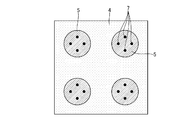
- FIG. 12 is a top view showing the antenna device 1C.
- the antenna device 1C is, for example, a four-element array antenna, and includes an antenna substrate 2 that radiates a signal radio wave into space through a patch element 5, and a feeding substrate 3 that feeds a signal to the antenna substrate 2.
- the antenna board 2, the power feeding board 3, and the dielectric 8 are provided with through holes 41 through which the screws 40 pass when they are stacked.
- the antenna board 2 and the power feeding board 3 in a state where the dielectric 8 is sandwiched are fixed. Since it is necessary to pass the screw 40 through the through hole 41 in the antenna device 1C, the opening diameter R2 of the through hole 41 is formed to be larger than the diameter R1 of the screw 40, as shown in FIG.
- the dimension of the feeding conductor 13C is formed to be larger than the dimension of the feeding conductor 6C by the difference between the diameter R1 of the screw 40 and the opening diameter R2 of the through hole 41.
- the facing area of the feeding conductor 6C and the feeding conductor 13C changes. It can be suppressed and the deterioration of the reflection characteristics accompanying this can be reduced.
- the antenna device 1C even if the dimension of the feeding conductor 6C is formed to be larger than the dimension of the feeding conductor 13C by the difference between the diameter R1 of the screw 40 and the opening diameter R2 of the through hole 41, the same effect can be obtained. can get.
- FIG. 13 is a side perspective view showing the antenna device 1D which is a modified example of the antenna device 1C, and the same components as those in FIG. 1 are designated by the same reference numerals and detailed description thereof will be omitted.
- FIG. 14 is a top view showing the antenna device 1D.
- the antenna device 1D is, for example, a four-element array antenna, and includes an antenna substrate 2 that radiates a signal radio wave into space through a patch element 5, and a feeding substrate 3 that feeds a signal to the antenna substrate 2.
- the frame member 42 integrally supports the antenna substrate 2, the feeding substrate 3, and the dielectric 8 in the state where the dielectric 8 is sandwiched between the antenna substrate 2 and the feeding substrate 3. It is fixed.
- the antenna substrate 2, the feeding substrate 3, and the dielectric 8 need to be housed in the frame member 42. Therefore, as shown in FIG. 14, the inner dimension R3 of the frame member 42 is the antenna substrate 2, The power feeding board 3 and the dielectric 8 are formed to be larger than the external dimensions L1.
- the dimension of the feeding conductor 13D is formed to be larger than the dimension of the feeding conductor 6D by the difference between the outer dimension L1 and the inner dimension R3.
- the antenna substrate 2 and the feeding substrate 3 are displaced by the difference between the external dimension L1 and the inner dimension R3, the change in the facing area between the feeding conductor 6D and the feeding conductor 13D is suppressed. It is possible to reduce the deterioration of the reflection characteristics due to the above.
- the antenna device 1D the same effect can be obtained even if the dimension of the feeding conductor 6D is formed to be larger than the dimension of the feeding conductor 13D by the difference between the external dimension L1 and the inner dimension R3.
- FIG. 15 is a plan view showing an example of the feeding conductor 6C of the antenna substrate 2 in the antenna device 1C.
- FIG. 16 is a plan view showing an example of the power feeding conductor 13C of the power feeding substrate 3 in the antenna device 1C.
- the misalignment between the antenna substrate 2 and the feeding substrate 3 is caused by the difference between the diameter R1 of the screw 40 and the opening diameter R2 of the through hole 41 as a play. Therefore, since the screw 40 moves in the through hole 41, the individual screw fastening portions are displaced in a circular range when viewed from above.
- the feeding conductor having a larger dimension has a circular shape as shown in FIGS. 15 and 16.
- the feeding conductor having the larger dimension can be formed with the minimum size including the range in which the misalignment can occur, so that the layout of the feeding structure can be saved.
- FIG. 17 is a plan view showing an example of the feeding conductor 6D of the antenna substrate 2 in the antenna device 1D.
- FIG. 18 is a plan view showing an example of the power feeding conductor 13D of the power feeding substrate 3 in the antenna device 1D.
- the positional deviation between the antenna substrate 2 and the feeding substrate 3 is caused by the difference between the external dimension L1 and the inner dimension R3 as a play. Therefore, the multilayer board in which the antenna board 2 and the power feeding board 3 are multilayered with the dielectric 8 sandwiched therein moves inside the frame member 42, and the position shift occurs in a rectangular range when viewed from the upper surface.
- the feeding conductor having a larger dimension has a rectangular shape as shown in FIGS. 17 and 18.
- the feeding conductor having the larger dimension can be formed with the minimum size including the range in which the misalignment can occur, so that the layout of the feeding structure can be saved.
- the antenna device 1C includes a through hole 41 penetrating the antenna board 2, the feeding board 3 and the dielectric 8, and the antenna board 2 and the feeding board 3 passing through the through hole 41.
- a screw 40 for fixing the dielectric 8 in a sandwiched state is provided.
- the antenna device 1C can fix the antenna substrate 2, the feeding substrate 3, and the dielectric 8 by the screws 40 and the through holes 41.
- the antenna device 1D supports the antenna substrate 2, the feeding substrate 3 and the dielectric 8 inside, and integrally fixes the dielectric 8 in a state of sandwiching the dielectric 8 between the antenna substrate 2 and the feeding substrate 3.
- a frame member 42 is provided. In the antenna device 1D, the antenna substrate 2, the feeding substrate 3, and the dielectric 8 can be fixed by the frame member 42.
- FIG. 19 is a side perspective view showing the antenna device 1E according to the fifth embodiment, and the same components as those in FIG. 1 are designated by the same reference numerals, and detailed description thereof will be omitted.
- FIG. 20 is an exploded perspective view showing a substrate of each layer in the antenna device 1E.
- the antenna device 1E is, for example, a four-element array antenna, and includes an antenna substrate 2 that radiates a signal radio wave into space through a patch element 5, and a feeding substrate 3A that feeds a signal to the antenna substrate 2.
- the power supply substrate 3A is a multilayer substrate in which a substrate 9 and a substrate 10 having substantially the same thickness are bonded in a plurality of stages (two stages in FIG. 19) by an adhesive layer 11.
- a main plate 12 and a feeding conductor 13 are provided on the main surface of the feeding board 3A on the antenna board 2 side.
- the power feeding unit 16a and the power feeding unit 16b are provided on the main surface of the power feeding board 3A on the opposite side of the antenna board 2.
- the 4-distribution synthesis circuit 15 and the feeding unit 16b are electrically connected by a vertical feeding unit 17.
- a 4-distribution synthesis circuit 15a is provided among the substrates constituting the feeding substrate 3A.
- the 4-distribution synthesis circuit 15a is composed of a triplate line, distributes a signal to be transmitted to the patch element 5, and synthesizes a signal from the patch element 5.
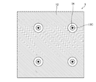
- FIG. 21 is a top view showing the patch element 5 of the antenna device 1E.
- FIG. 22 is a top view showing a modified example of the patch element 5 of the antenna device 1E.
- the patch element 5 may be probe-fed at two feeding points as shown in FIGS. 19, 20 and 21, or may be probe-fed at four feeding points as shown in FIG. ..
- the patch element 5 fed at two or more feeding points can make a signal radiated as a radio wave circularly polarized, bipolarized, or lowly cross-polarized.
- the multi-layered power supply substrate 3A can be provided with a filter that blocks signals of unnecessary frequency components by, for example, being configured by a triplate line, and a phase difference can be added to the signals fed to each patch element 5.
- a power supply circuit such as a hybrid circuit can be provided.
- the antenna device 1E in which the feeding board 3A having such a circuit is combined with the antenna board 2 can realize an antenna having a thin flat surface and high functionality.
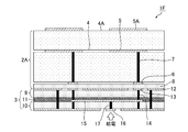
- FIG. 23 is a side perspective view showing the antenna device 1F which is a modified example of the antenna device 1E, and the same components as those in FIG. 1 are designated by the same reference numerals and detailed description thereof will be omitted.
- the antenna device 1F is, for example, a 4-element array antenna, and includes an antenna substrate 2A and a feeding substrate 3.
- the antenna substrate 2A is configured by stacking a dielectric substrate 4A, which is a non-exciting element substrate, on a dielectric substrate 4 in order to widen the frequency band used by the antenna device 1F. ..
- a non-excited patch element 5A is provided on the main surface of the dielectric substrate 4A on the opposite side of the dielectric substrate 4 from the dielectric substrate 4.
- the signal fed from the feeding board 3 to the antenna board 2A is radiated into space through the patch element 5.
- the antenna substrate 2A is configured by stacking a plurality of substrates, but is not a multilayer substrate including the power feeding substrate 3. Therefore, the stress generated when the antenna substrate 2A and the feeding substrate 3 are attached to each other is absorbed by the misalignment of both substrates. Therefore, the antenna device 1F realizes a thin antenna because warpage does not occur even if a substrate having the same thickness as the antenna substrate 2A is not multi-layered on the main surface of the feeding substrate 3 opposite to the antenna substrate 2A. be able to.
- the power feeding substrate 3A is a multilayer substrate composed of a plurality of dielectric substrates. Since various circuits can be provided on the power feeding board 3A, the antenna device 1E can realize an antenna having a thin flat surface and high functionality.
- the antenna substrate 2A is a multilayer substrate composed of a plurality of dielectric substrates. Since the antenna substrate 2A becomes thicker, the frequency band used by the antenna device 1F is widened.
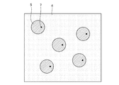
- FIG. 24 is a top view showing Example 1 of the patch element.
- FIG. 25 is a top view showing Example 2 of the patch element.
- FIG. 26 is a top view showing Example 3 of the patch element.
- FIG. 27 is a top view showing Example 4 of the patch element.
- the antenna device shown in the first to fifth embodiments may be an antenna in which a single patch element 5 is provided on the dielectric substrate 4, or is shown in FIG. 25. As shown, it may be a linear array antenna in which a plurality of patch elements 5 are linearly arranged on a dielectric substrate 4. Further, the antenna device shown in the first to fifth embodiments may be an antenna in which a plurality of patch elements 5 are triangularly arranged on the dielectric substrate 4, as shown in FIG. 26.
- the antenna may be an antenna in which a plurality of patch elements 5 are aperiodically arranged on the dielectric substrate 4.
- the antenna devices shown in the first to fifth embodiments can realize various arrangements of the patch elements 5, and the degree of freedom in antenna design is high.
- the antenna device according to the present disclosure can be used as a radar device, for example.
- 1,1A, 1B, 1C, 1D, 1E, 1F antenna device 2,2A antenna board, 3,3A power supply board, 4,4A dielectric board, 5 patch element, 5A non-excitation patch element, 6,6A, 6B , 6C, 6D feed conductor, 7 through hole, 8 dielectric, 9, 10 substrate, 11 adhesive layer, 12 main plate, 13, 13A, 13B, 13C, 13D feed conductor, 14, 17 vertical feed section, 15, 15a 4 Distribution synthesis circuit, 16, 16a, 16b power feeding part, 40 screws, 41 through holes, 42 frame members, 100 loads, 101 inductance components, 102 capacitance components.
Landscapes
- Waveguide Aerials (AREA)
- Variable-Direction Aerials And Aerial Arrays (AREA)
Priority Applications (2)
| Application Number | Priority Date | Filing Date | Title |
|---|---|---|---|
| JP2022502021A JPWO2021186596A1 (https=) | 2020-03-18 | 2020-03-18 | |
| PCT/JP2020/011863 WO2021186596A1 (ja) | 2020-03-18 | 2020-03-18 | アンテナ装置 |
Applications Claiming Priority (1)
| Application Number | Priority Date | Filing Date | Title |
|---|---|---|---|
| PCT/JP2020/011863 WO2021186596A1 (ja) | 2020-03-18 | 2020-03-18 | アンテナ装置 |
Publications (1)
| Publication Number | Publication Date |
|---|---|
| WO2021186596A1 true WO2021186596A1 (ja) | 2021-09-23 |
Family
ID=77770904
Family Applications (1)
| Application Number | Title | Priority Date | Filing Date |
|---|---|---|---|
| PCT/JP2020/011863 Ceased WO2021186596A1 (ja) | 2020-03-18 | 2020-03-18 | アンテナ装置 |
Country Status (2)
| Country | Link |
|---|---|
| JP (1) | JPWO2021186596A1 (https=) |
| WO (1) | WO2021186596A1 (https=) |
Citations (3)
| Publication number | Priority date | Publication date | Assignee | Title |
|---|---|---|---|---|
| JP2008066838A (ja) * | 2006-09-05 | 2008-03-21 | Mitsubishi Electric Corp | アンテナ装置 |
| US20190348749A1 (en) * | 2018-05-11 | 2019-11-14 | Intel IP Corporation | Antenna boards and communication devices |
| JP2019537850A (ja) * | 2016-09-01 | 2019-12-26 | ウェハー エルエルシーWafer Llc | ソフトウェア制御のアンテナ |
Family Cites Families (1)
| Publication number | Priority date | Publication date | Assignee | Title |
|---|---|---|---|---|
| WO2019189050A1 (ja) * | 2018-03-30 | 2019-10-03 | 株式会社村田製作所 | アンテナモジュールおよびそれを搭載した通信装置 |
-
2020
- 2020-03-18 JP JP2022502021A patent/JPWO2021186596A1/ja active Pending
- 2020-03-18 WO PCT/JP2020/011863 patent/WO2021186596A1/ja not_active Ceased
Patent Citations (3)
| Publication number | Priority date | Publication date | Assignee | Title |
|---|---|---|---|---|
| JP2008066838A (ja) * | 2006-09-05 | 2008-03-21 | Mitsubishi Electric Corp | アンテナ装置 |
| JP2019537850A (ja) * | 2016-09-01 | 2019-12-26 | ウェハー エルエルシーWafer Llc | ソフトウェア制御のアンテナ |
| US20190348749A1 (en) * | 2018-05-11 | 2019-11-14 | Intel IP Corporation | Antenna boards and communication devices |
Also Published As
| Publication number | Publication date |
|---|---|
| JPWO2021186596A1 (https=) | 2021-09-23 |
Similar Documents
| Publication | Publication Date | Title |
|---|---|---|
| JP6129857B2 (ja) | 偏波共用アンテナ | |
| US11171421B2 (en) | Antenna module and communication device equipped with the same | |
| US7626549B2 (en) | Compact planar antenna for single and multiple polarization configurations | |
| WO2018230475A1 (ja) | アンテナモジュールおよび通信装置 | |
| WO2014073355A1 (ja) | アレーアンテナ | |
| CN109478721B (zh) | 天线、具有一个或更多个天线的装置及通信装置 | |
| US7532171B2 (en) | Millimeter wave electronically scanned antenna | |
| WO2018173750A1 (ja) | アンテナモジュール及び通信装置 | |
| US5442367A (en) | Printed antenna with strip and slot radiators | |
| CN109565112B (zh) | 天线装置 | |
| US20220359995A1 (en) | Patch antenna | |
| US20170317422A1 (en) | Low Profile Wideband Planar Antenna Element With Integrated Baluns | |
| JPWO2012042740A1 (ja) | 構造体及び配線基板 | |
| US20170317421A1 (en) | Low Profile Wideband Planar Antenna Element | |
| US9716305B2 (en) | Balun | |
| CN115769438A (zh) | 天线装置 | |
| CN114982066A (zh) | 天线装置 | |
| CN105449354B (zh) | 一种采用费马‑阿基米德螺旋槽线双过孔电磁带隙结构的低互耦天线阵 | |
| US11557820B2 (en) | Phase shifter having a substrate with a signal feed line thereon and including a replaceable dielectric board fixed to the substrate and covering the feed line | |
| US20250329931A1 (en) | Antenna element having a plurality of radiator patches | |
| GB2397697A (en) | Folded flexible antenna array | |
| CN117136470A (zh) | 天线及电子设备 | |
| WO2021186596A1 (ja) | アンテナ装置 | |
| CN114142224B (zh) | 一种高增益圆极化天线 | |
| US20240021980A1 (en) | Connector-less printed circuit board mounted antenna |
Legal Events
| Date | Code | Title | Description |
|---|---|---|---|
| 121 | Ep: the epo has been informed by wipo that ep was designated in this application |
Ref document number: 20926216 Country of ref document: EP Kind code of ref document: A1 |
|
| ENP | Entry into the national phase |
Ref document number: 2022502021 Country of ref document: JP Kind code of ref document: A |
|
| NENP | Non-entry into the national phase |
Ref country code: DE |
|
| 122 | Ep: pct application non-entry in european phase |
Ref document number: 20926216 Country of ref document: EP Kind code of ref document: A1 |