WO2021182223A1 - プロセッサ及びデータ経路再構成方法 - Google Patents
プロセッサ及びデータ経路再構成方法 Download PDFInfo
- Publication number
- WO2021182223A1 WO2021182223A1 PCT/JP2021/008133 JP2021008133W WO2021182223A1 WO 2021182223 A1 WO2021182223 A1 WO 2021182223A1 JP 2021008133 W JP2021008133 W JP 2021008133W WO 2021182223 A1 WO2021182223 A1 WO 2021182223A1
- Authority
- WO
- WIPO (PCT)
- Prior art keywords
- data
- arithmetic
- path
- invalidated
- failure
- Prior art date
- Legal status (The legal status is an assumption and is not a legal conclusion. Google has not performed a legal analysis and makes no representation as to the accuracy of the status listed.)
- Ceased
Links
Images





Classifications
-
- G—PHYSICS
- G06—COMPUTING OR CALCULATING; COUNTING
- G06F—ELECTRIC DIGITAL DATA PROCESSING
- G06F15/00—Digital computers in general; Data processing equipment in general
- G06F15/16—Combinations of two or more digital computers each having at least an arithmetic unit, a program unit and a register, e.g. for a simultaneous processing of several programs
- G06F15/177—Initialisation or configuration control
Definitions
- This disclosure relates to a processor and a data path reconstruction method.
- a multi-core processor equipped with a plurality of arithmetic units such as a CPU (Central Processing Unit) and a GPU (Graphics Processing Unit) has become common.
- core processors such as a CPU (Central Processing Unit) and a GPU (Graphics Processing Unit)
- DCLS Dual Core Lock-Step
- PE Processing Element
- Such a PE array is designed on the premise that all PEs operate normally. Therefore, if any one of the PEs constituting the PE array fails, the operation is generally not stopped or functioned. For example, in a processor composed of a CPU and a GPU, if the PE constituting the GPU fails, the function of the GPU is lost, so that the performance as a processor is significantly deteriorated. In addition, if a PE failure is discovered during the manufacturing stage of the processor, the PE array containing the PE may be shipped as a lower grade processor that does not function.
- the processor of one aspect of the present disclosure is a processor in which a plurality of arithmetic units are arranged in a two-dimensional manner to perform parallel processing, and the failure detection unit for detecting the failure of the arithmetic units and the calculation by the failure detection unit.
- the invalidated machine is provided with an invalidation unit for invalidating all of the machines included in at least one of a row and a column including the failed machine. Execute the process without using it.
- FIG. 1 is a schematic configuration diagram of a processor of the embodiment.
- FIG. 2 is a schematic diagram showing the reconstruction of the data path of the embodiment, (A) shows the data path in the normal state, and (B) shows the data path when a failure occurs in PE.
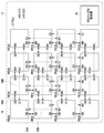
- FIG. 3 is a schematic configuration diagram of the PE array of the embodiment.
- FIG. 4 is a schematic configuration diagram of PE of the embodiment.
- FIG. 5 is a schematic diagram showing a failure detection signal output from the PE failure detection unit of the embodiment.
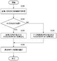
- FIG. 6 is a flowchart showing the flow of the data path reconstruction process of the embodiment.
- FIG. 7A and 7B are schematic views showing the operating state of the PE array of the embodiment, FIG. 7A shows the operating state of the PE array under normal conditions, and FIG. 7B shows the operating state of the PC array when one row of arrays is invalidated. The operating state is shown, and (C) shows the operating state of the PE array when the array in one row is invalidated.
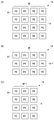
- FIG. 8 is a schematic diagram showing a data pattern corresponding to the operating state of the PE array of the embodiment, (A) shows a data pattern corresponding to the PE array in the normal state, and (B) invalidates the array in one row. The data pattern when the data pattern is changed is shown, and (C) shows the data pattern when the array in one row is invalidated.
- FIG. 1 is a schematic configuration diagram of the processor 10 of the present embodiment.
- the processor 10 of the present embodiment is a multi-core processor composed of four CPUs (Central Processing Units) 12 and one GPU (Graphics Processing Unit) 14 as arithmetic units (core processors).
- CPUs Central Processing Units
- GPU Graphics Processing Unit
- the GPU 14 is composed of a PE array 18 in which a plurality of processing elements (hereinafter referred to as “PE”) 16 which are arithmetic units are arranged two-dimensionally.
- the PE array 18 performs parallel distributed processing while adjacent PE 16s exchange data.
- the processor 10 of the present embodiment processes the image data input from the storage device 20 and outputs the processing result.
- the data exchanged between the PEs 16 constituting the GPU 14 (PE array 18) is, for example, an overlapping region, a weighting coefficient, and the like used for the convolution calculation in the image data processing.
- the processing performed by the processor 10 may be used not only for image data processing but also for other processing such as machine learning using a neural network.
- 16 PE 16s are arranged two-dimensionally in 4 rows ⁇ 4 columns, but this is an example, and the PE 16 constituting the PE array 18
- the number, number of rows and number of columns are not limited.
- the PE array 18 performs parallel distributed processing by a plurality of PEs 16. Therefore, if even one PE 16 fails, conventionally, the entire PE array 18 is invalidated, and the performance of the processor 10 is significantly reduced.
- the processor 10 of the present embodiment invalidates all of the PE 16 included in at least one of the row and the column including the failed PE 16, and processes without using the invalidated PE 16 (hereinafter referred to as “invalidated PE”). To execute. As a result, the processor 10 can be used even if any of the plurality of PE16s arranged in two dimensions fails.
- FIG. 2 is a schematic diagram showing the reconstruction of the data path of the present embodiment.
- FIG. 2 only the data path from the leftmost PE 16 to the adjacent PE 16 on the right side is shown, but this merely omits the data path of the other PE 16, and the other adjacent PE 16 Data can be exchanged between each other.
- FIG. 2A shows a data path when the PE 16 constituting the PE array 18 has not failed, that is, when it is normal. As shown in FIG. 2A, when no failure has occurred, the PE 16 exchanges data with the adjacent PE 16.
- FIG. 2B shows a data path when a failure occurs in PE16.
- all PE16s included in the column including PE16X in which a failure has occurred are invalidated (PE16s hatched by diagonal lines).
- the invalidated PE and the adjacent PE 16 do not exchange data with the invalidated PE, but exchange data with another PE 16 sandwiching the invalidated PE.
- the processor 10 of the present embodiment invalidates all the PE 16s included in the row or column including the failed PE 16, and exchanges data between the non-failed PE 16s so as to bypass the invalidated PE.
- FIG. 3 is a schematic configuration diagram of the PE array 18 of the present embodiment.
- the PE 16 constituting the PE array 18 has the PE 16 in the upper left direction of the paper surface as PE 00, the right direction of the paper surface as the x direction, and the lower direction of the paper surface as the y direction, and the arrangement position is indicated as PExy. Further, in FIG. 3, in each PE16, the upward direction of the paper surface is described as "N”, the downward direction of the paper surface is described as “S”, the right direction of the paper surface is described as "E”, and the left direction of the paper surface is described as "W”. Notated.
- the PE 16 of the present embodiment has a normal data path 30A for exchanging data with another adjacent PE 16 and an invalid data path 30B for exchanging data with every other adjacent PE 16.
- a normal data path 30A for exchanging data with another adjacent PE 16
- an invalid data path 30B for exchanging data with every other adjacent PE 16.
- PE16 adjacent to each other on the left and right is connected to the path E0-W0 by the normal data path 30A
- PE16 adjacent to each other on the upper and lower sides is connected to the path S0-N0 by the normal data path 30A. Will be done.
- the PE16s that are two adjacent to each other on the left and right are connected to the path E1-W1 by the invalid data path 30B
- the PE16s that are two adjacent to each other on the upper and lower sides are connected to the path S1-N1 by the invalid data path 30B.
- the PE array 18 includes a PE enable generator 32.
- the PE enable generator 32 invalidates all the PE 16s contained in the row or column containing the failed PE 16.
- the PE enable generator 32 generates an enable signal PExy_EN for this purpose and outputs it to the PE 16 for invalidating it.
- the enable signal PExy_EN is “0”, the operation of the PE 16 to which the enable signal PExy_EN is input is stopped.
- the PE enable generator 32 is invalid so as to exchange data with another PE 16 using the invalid data path 30B without exchanging data with the invalidated PE using the normal data path 30A.
- the PE enable generator 32 generates an interface selection signal for this purpose and outputs it to the PE 16.
- the PE 16 to which the interface selection signal is input switches the data exchange path from the normal data path 30A to the invalid data path 30B. The details of the interface selection signal will be described later.
- the PE enable generator 32 notifies the user that a failure has occurred in the PE array 18 via the user interface (not shown) when the PE 16 is disabled. As a result, the user can recognize the failure of the PE array 18 and take measures such as repair.
- the normal data path 30A and the invalid data path 30B for exchanging data between PE16s adjacent to each other in the oblique direction are not shown, but the PE array 18 exchanges data in the oblique direction.
- a data path may be provided.
- FIG. 4 is a schematic configuration diagram of PE16 of the present embodiment.
- the PE 16 includes an ALU (Arithmetic and Logic Unit) 40, a register 42, a RAM (Random Access Memory) 44, a PE failure detection unit 46, an interface unit 48N, 48E, 48W, 48S, and a control unit 50.
- ALU Arimetic and Logic Unit
- register 42 a register for storing data
- RAM Random Access Memory
- the ALU40 performs an operation based on the data from the register 42 and outputs the operation result to the register 42.
- the register 42 inputs / outputs data to / from the ALU 40, the RAM 44, and the interface unit 48, and stores the data.
- the RAM 44 inputs and outputs data to and from the register 42 and the interface unit 48, and stores the data.
- the PE failure detection unit 46 detects a failure of the PE 16 and outputs the detection result as a failure detection signal to the PE enable generator 32.
- FIG. 5 is a schematic diagram showing an example of a failure detection signal output from the PE failure detection unit 46.
- the failure detection signal PExy_Diag is composed of PExy that specifies the arrangement position xy of the PE 16 that includes itself, and "0" to "5" that are identifiers that indicate the presence or absence of a failure.
- the PE failure detection unit 46 outputs "0" as a failure detection signal together with the arrangement position xy of the PE 16 when there is no failure in the PE 16. On the other hand, when a failure occurs in the PE 16, the PE failure detection unit 46 outputs any of "1” to "5" together with the arrangement position xy of the PE 16 as a failure detection signal.
- the "1" to “5" indicate the faulty part, and the “1" indicates that the faulty part is one of the control unit 50, the ALU40, the register 42, and the RAM 44. That is, when the failure detection signal is "1", it means that the PE 16 itself is out of order.
- failure detection signal When the failure detection signal is "2", it indicates that the failure location is the N0 path, and when the failure detection signal is "3", it indicates that the failure location is the S0 path, and the failure detection signal is "4". When the case is, it indicates that the failure point is the W0 path, and when the failure detection signal is “5”, it indicates that the failure point is the E0 path. That is, when the failure detection signal is "2" to "5", it means that any one of the normal data paths 30A has failed.
- the PE failure detection signal can identify not only the presence or absence of failure of PE16 itself but also the failure route.
- the PE failure detection signal shown in FIG. 4 is an example and is not limited to this.
- the interface unit 48 is an input / output unit for exchanging data with another PE 16 adjacent to one or two.
- the interface unit 48 of the present embodiment has two systems, one input / output unit (N0, E0, W0, S0) for one adjacency and one input / output unit (N1, E1, W1, S1) for two adjacencies.
- the control unit 50 decodes the program for PE16, generates control signals to the ALU 40, the register 42, and the RAM 44, and outputs the control signals to these. Further, the control unit 50 receives the input of the enable signal PExy_EN from the PE enable generator 32. Then, for example, when the enable signal is "0", the control unit 50 stops the operation of the PE 16 including itself and invalidates it.
- control unit 50 receives an interface selection signal from the PE enable generator 32.
- interface selection signals there are four types of interface selection signals, PExy_Nsel, PExy_Esel, PExy_Wsel, and PExy_Ssel, and Nsel, Esel, Wsel, and Ssel correspond to the interface units 48N, 48E, 48W, and 48S, respectively.
- the interface selection signal is "0"
- the normal data path 30A connected to the input / output units N0, E0, W0, S0 for 1 adjacency is used.
- the interface selection signal is "1”
- the invalid data path 30B connected to the two adjacent input / output units N1, E1, W1, S1 is used.
- FIG. 6 is a flowchart showing the flow of the data path reconstruction process of the present embodiment.
- the PE failure detection unit 46 included in any of the PE 16s constituting the PE array 18 detects the failure of the PE 16, and the failure detection signal PExy_Diag is input to the PE enable generator 32. If so, it is executed by the PE enable generator 32. Further, the data path reconstruction process is executed by a program stored in the recording medium included in the processor 10. When this program is executed, the method corresponding to the program is executed.
- step 100 the failed PE 16 and its fault location are identified based on the fault detection signal PExy_Diag from the PE fault detection unit 46.
- step 102 it is determined whether or not the PE 16 itself has failed based on the failure detection signal PExy_Diag, and if the determination is affirmative, the process proceeds to step 104, and if the determination is negative, the process proceeds to step 106.
- step 104 an enable signal is output to the corresponding PE 16 so as to invalidate all the PE 16s in the row or column including the failed PE 16, and the process proceeds to step 108.
- the control unit 50 of the PE 16 to which the enable signal is input stops the operation of the PE 16 including itself.
- whether the invalidation PE16 is a row or a column may be determined by a preset method. For example, for the first PE16 failure, all PE16s in the column containing the failed PE16 are invalidated, and for the second PE16 failure, the row containing the failed PE16 is invalidated. It is assumed that all PE16s are invalidated. This makes it possible to prevent all PE16s in the two adjacent rows or the two adjacent columns from being invalidated even if the two PE16s constituting the PE array 18 fail. That is, the PE enable generator 32 determines the PE 16 to be invalidated so that when a plurality of PE 16s fail, the rows and columns to be invalidated intersect each other without being adjacent to each other.
- whether the invalidated PE is a row or a column may be determined by the configuration of the PE array 18. For example, in the case of the PE array 18 of N rows> M columns, the invalidated PE is set as the row, and in the case of the PE array 18 of N rows ⁇ M columns, the invalidated PE is set as the column.
- step 106 which is the migration destination in this case, the PE enable generator 32 is the target PE 16 so as to invalidate all the PE 16 in the row or column including the PE 16 of the data exchange destination via the normal data path 30A.
- the enable signal is output to, and the process proceeds to step 108.
- step 106 An example of the process according to step 106 will be described with reference to FIG. For example, if a failure is detected in PE11 and it is the normal data path 30A of the S0 path, PE16 of PE02 to PE22, which is the line below PE11, is regarded as an invalidated PE. If a failure is found in the normal data path 30A of the E0 path of PE11, PE16 of PE20 to PE23, which is the right column of PE11, is regarded as an invalidated PE.
- the PE enable generator 32 outputs an interface selection signal for selecting the invalid data path 30B for the PE 16 adjacent to the invalidated PE.
- the control unit 50 to which the interface selection signal is input selects the invalid data path 30B as the data path of the PE 16 including itself, and ends the data path reconstruction process.
- the PE 16 to which the interface selection signal is input bypasses the invalidated PE and exchanges data with other PE 16s adjacent to each other.
- the processor 10 of the present embodiment changes the data path so as to bypass the invalidated PE and exchange data between the PEs 16, so that even if a failure occurs in any of the plurality of PEs 16, the PE array 18 can be used.
- FIG. 7 is a schematic view showing an operating state of the PE array 18 of N rows and M columns of the present embodiment.
- FIG. 7A shows the operating state of the PE array 18 in the normal state, and all 16 PE16s in 4 rows and 4 columns are operating.
- FIG. 7 (B) shows the operating state of the PE array 18 when one row of PE 16 is disabled
- FIG. 7 (C) shows the operating state of the PE array 18 when one row of PE 16 is disabled.
- the PE array 18 when one row of PE16 is invalidated, the PE array 18 becomes N-1 row and M column, and in the example of FIG. 7B, a total of 12 PE16s of 3 rows and 4 columns are formed. It will work. Further, as shown in FIG. 7 (C), when the PE 16 in one column is invalidated, the PE array 18 becomes N rows and M-1 columns, and in the example of FIG. 7 (B), a total of 12 in 4 rows and 3 columns. PE16 will operate.
- FIG. 8 is a schematic diagram showing a data pattern 60 corresponding to the operating state of the PE array 18 of the present embodiment.
- the data pattern 60 shows a mode of dividing the data processed by each of the plurality of PEs 16, and is stored in the storage device 20 as an example.
- the data pattern 60 is not limited to this, and the data pattern 60 is stored in the processor 10. It may be stored in the provided storage medium.
- the data pattern 60 shown in FIG. 8 is, for example, a division pattern for dividing one image data acquired by an in-vehicle camera into a plurality of areas, and each image data area divided by the data pattern 60 is divided into a plurality of areas. Distributed parallel processing is performed on each of the plurality of PE16s.
- the area indicated by the diagonal line in the data pattern 60 is an overlapping area used by a convolution operation or the like.
- the data pattern 60 of the present embodiment includes a data pattern 60A used when the PE 16 constituting the PE array 18 has no failure, and data patterns 60B and 60C used when the PE 16 is invalidated. That is, FIG. 8 (A) shows the data pattern 60A corresponding to the PE array 18 in the normal state, FIG. 8 (B) shows the data pattern 60B when one row of PE 16 is invalidated, and FIG. 8 (C) shows the data pattern 60B. The data pattern 60C when one row of PE16 is invalidated is shown.
- FIG. 8 (A), (B), (C) corresponds to the above-mentioned FIGS. 7 (A), (B), (C). That is, the data pattern 60A is a data pattern 60 used when the plurality of PE 16s constituting the PE array 18 have no failure, and the data patterns 60B and 60C are included in the row or column in which the failure of the PE 16 is detected. It is a data pattern 60 used when all of PE 16 is invalidated.
- the processor 10 of the present embodiment prepares the data patterns 60B and 60C corresponding to the case where the PE 16 is invalidated in advance, so that the use of the PE array 18 in which the row or column is invalidated PE can be performed by a simple process. You can continue. Further, in reality, it is difficult to assume that a plurality of PE16s will fail. Therefore, as an example, in addition to the data pattern 60A, when one row is an invalidated PE and one column is an invalidated PE.
- the two types of data patterns 60 of the data pattern 60C may be stored in the storage device 20.
- Whether to use the data pattern 60B or the data pattern 60C when the PE 16 is invalidated is selected by the PE enable generator 32 as an example.
- the processor 10 may be provided with at least one arithmetic unit composed of the PE array 18, and the number of arithmetic units such as the CPU 12 and the GPU 14 is not limited.
Landscapes
- Engineering & Computer Science (AREA)
- Computer Hardware Design (AREA)
- Theoretical Computer Science (AREA)
- Software Systems (AREA)
- Physics & Mathematics (AREA)
- General Engineering & Computer Science (AREA)
- General Physics & Mathematics (AREA)
- Multi Processors (AREA)
- Hardware Redundancy (AREA)
Abstract
複数のPE(16)が2次元状に配列されて並列処理を行うプロセッサ(10)が、PE(16)の故障が検出された場合に、故障したPE(16)を含む行及び列の少なくとも一方に含まれるPE(16)の全てを無効化し、無効化したPE(16)を用いることなく処理を実行する。このため、PE(16)は、隣接する他のPE(16)とデータ交換を行う正常時データ経路(30A)と、一つ置きで隣接する他のPE(16)とデータ交換を行う無効時データ経路(30B)とを有する。そして、無効化されたPE(16)と隣接するPE(16)は、無効化されたPE(16)とのデータ交換を正常時データ経路(30A)を用いて行わずに、無効時データ経路(30B)を用いて他のPE(16)とのデータ交換を行う。
Description
本出願は、2020年3月11日に出願された特許出願番号2020-042174号に基づくものであって、その優先権の利益を主張するものであり、その特許出願のすべての内容が、参照により本明細書に組み入れられる。
本開示は、プロセッサ及びデータ経路再構成方法に関する。
近年、CPU(Central Processing Unit)やGPU(Graphics Processing Unit)等の演算装置(コアプロセッサ)を複数備えたマルチコアプロセッサが一般的となっている。このようなプロセッサには、特許文献1に開示されているように、コアの動作を監視するためにDCLS(Dual Core Lock-Step)のような故障検知機構を備えたものもある。そして、故障が検出されたコアプロセッサは、その動作が停止される。
ここで、GPUのように2次元状に複数の演算機(Processing Element、以下「PE」という。)が配列されて構成されるPEアレイは、複数のPEによる並列処理を可能としている。
このようなPEアレイは、全てのPEが正常に動作することを前提として設計されている。このため、PEアレイを構成するPEのうち一つでも故障すると、一般的に動作を停止又は機能させない。例えば、CPUとGPUで構成されるプロセッサでは、GPUを構成するPEが故障した場合にGPUの機能が失われるので、プロセッサとしての性能が大幅に低下してしまう。また、プロセッサの製造段階でPEの故障が発見されると、そのPEを含むPEアレイを機能させない下位グレードのプロセッサとして出荷されたりもする。
本開示は、2次元状に配列された複数の演算機の何れかに故障が発生しても使用を可能とする、プロセッサ及びデータ経路再構成方法を提供することを目的とする。
本開示の一態様のプロセッサは、複数の演算機が2次元状に配列されて並列処理を行うプロセッサであって、前記演算機の故障を検出する故障検出部と、前記故障検出部によって前記演算機の故障が検出された場合に、故障した前記演算機を含む行及び列の少なくとも一方に含まれる前記演算機の全てを無効化する無効化部と、を備え、無効化した前記演算機を用いることなく処理を実行する。
本開示によれば、2次元状に配列された複数の演算機の何れかに故障が発生しても使用を可能とする。
本開示についての上記目的およびその他の目的、特徴や利点は、添付の図面を参照しながら下記の詳細な記述により、より明確になる。その図面は、
図1は、実施形態のプロセッサの概略構成図である。
図2は、実施形態のデータ経路の再構成を示す模式図であり、(A)は正常時のデータ経路を示し、(B)はPEに故障が発生した場合のデータ経路を示す。
図3は、実施形態のPEアレイの概略構成図である。
図4は、実施形態のPEの概略構成図である。
図5は、実施形態のPE故障検出部から出力される故障検出信号を示す模式図である。
図6は、実施形態のデータ経路再構成処理の流れを示すフローチャートである。
図7は、実施形態のPEアレイの動作状態を示す模式図であり、(A)は正常時のPEアレイにおける動作状態を示し、(B)は一行のアレイを無効化した場合のPCアレイの動作状態を示し、(C)は一列のアレイを無効化した場合のPEアレイの動作状態を示す。
図8は、実施形態のPEアレイの動作状態に対応するデータパターンを示す模式図であり、(A)は正常時のPEアレイに対応するデータパターンを示し、(B)は一行のアレイを無効化した場合のデータパターンを示し、(C)は一列のアレイを無効化した場合のデータパターンを示す。
以下、図面を参照して本開示の実施形態を説明する。なお、以下に説明する実施形態は、本開示を実施する場合の一例を示すものであって、本開示を以下に説明する具体的構成に限定するものではない。本開示の実施にあたっては、実施形態に応じた具体的構成が適宜採用されてよい。
図1は、本実施形態のプロセッサ10の概略構成図である。本実施形態のプロセッサ10は、一例として、演算装置(コアプロセッサ)として4つのCPU(Central Processing Unit)12と一つのGPU(Graphics Processing Unit)14によって構成されるマルチコアプロセッサである。
ここで、GPU14は、演算機である複数のプロセッシングエレメント(Processing Element、以下「PE」という。)16を2次元状に配列したPEアレイ18によって構成される。PEアレイ18は、隣接するPE16がデータ交換をしながら、並列分散処理を行う。
本実施形態のプロセッサ10は、一例として、記憶装置20から入力される画像データに対して処理を行い、処理結果を出力する。そして、GPU14(PEアレイ18)を構成するPE16同士が交換するデータは、一例として、画像データ処理における畳み込み演算に用いる重複領域や重み係数等である。なお、プロセッサ10が行う処理は、画像データ処理だけでなく、例えば、ニューラルネットワークを用いた機械学習等、他の処理に用いられてもよい。
また、図1等に示される本実施形態のPEアレイ18は、16個のPE16が4行×4列で2次元配列されているが、これは一例であり、PEアレイ18を構成するPE16の数、行数及び列数は限定されない。
PEアレイ18は、上述のように、複数のPE16によって並列分散処理を行うものである。このため、一つでもPE16が故障すると、従来では、PEアレイ18全体が無効化され、プロセッサ10としての性能が大幅に低下する。
このため、PE16が故障した場合であっても、故障したPE16のみを無効化してPEアレイ18の使用を継続することも考えられるものの、どのPE16が故障するかを事前に予測することはできない。このため、無効化したPE16を除外したPEアレイ18に対応するデータの配置方法やプログラムのパターンをn行×m列通り予め設計する必要がある。このような手法は、PEアレイ18を構成するPE16の数が増加すると、設計するべきパターンの数が膨大となり、現実的ではない。
そこで、本実施形態のプロセッサ10は、故障したPE16を含む行及び列の少なくとも一方に含まれるPE16の全てを無効化し、無効化したPE16(以下「無効化PE」という。)を用いることなく処理を実行する。これにより、プロセッサ10は、2次元状に配列された複数のPE16の何れかに故障が発生しても使用可能となる。
図2は、本実施形態のデータ経路の再構成を示す模式図である。なお、図2では、最も左側のPE16から右側に隣接するPE16へのデータ経路のみが表記されているが、これは他のPE16のデータ経路を省略しているに過ぎず、他の隣接するPE16同士等でもデータ交換が可能とされている。
図2(A)はPEアレイ18を構成するPE16に故障が発生していない場合、すなわち正常時のデータ経路を示す。図2(A)に示されるように、故障が発生していない場合には、PE16は隣接するPE16との間でデータ交換を行う。
一方、図2(B)はPE16に故障が発生した場合のデータ経路を示す。図2(B)の例では、一例として故障が発生したPE16Xを含む列に含まれる全てのPE16が無効とされる(斜線でハッチングされたPE16)。そして、無効化PEと隣接するPE16は、無効化PEとはデータ交換を行わずに、無効化PEを挟んだ他のPE16との間でデータ交換を行う。このように、本実施形態のプロセッサ10は、故障したPE16を含む行又は列に含まれるPE16全てを無効化し、故障していないPE16同士が無効化PEをバイパスするようにデータ交換を行う。
図3は、本実施形態のPEアレイ18の概略構成図である。
図3においてPEアレイ18を構成するPE16は、紙面左上方向のPE16をPE00として、紙面右方向をx方向とし、紙面下方向をy方向とし、PExyとのように配置位置が表記される。また、図3では、各PE16において紙面上方向が“N”と表記され、紙面下方向が“S”と表記され、紙面右方向が“E”と表記され、紙面左方向が“W”と表記される。
本実施形態のPE16は、隣接する他のPE16とデータ交換を行う正常時データ経路30Aと、一つ置きで隣接する他のPE16とデータ交換を行う無効時データ経路30Bとを有している。なお、以下の説明では、PE16が隣接することを1隣接といい、PE16が一つ置きで隣接することを2隣接という。
図3を参照すると、左右同士で1隣接するPE16は、正常時データ経路30Aによって経路E0-W0が接続され、上下同士で1隣接するPE16は、正常時データ経路30Aによって経路S0-N0が接続される。一方、左右同士で2隣接するPE16は、無効時データ経路30Bによって経路E1-W1が接続され、上下同士で2隣接するPE16は、無効時データ経路30Bによって経路S1-N1が接続される。
また、PEアレイ18は、PEイネーブル生成器32を備える。PEイネーブル生成器32は、PE16の故障が検出された場合に、故障したPE16を含む行又は列に含まれるPE16の全てを無効化する。なお、PEイネーブル生成器32は、このためのイネーブル信号PExy_ENを生成し、無効化させるPE16へ出力する。一例として、イネーブル信号PExy_ENが“0”の場合に、イネーブル信号PExy_ENが入力されたPE16の動作が停止される。
また、PEイネーブル生成器32は、正常時データ経路30Aを用いて無効化PEとのデータ交換を行わずに、無効時データ経路30Bを用いて他のPE16とのデータ交換を行うように、無効化PEに隣接するPE16へ出力する。なお、PEイネーブル生成器32は、このためにインターフェース選択信号を生成し、PE16へ出力する。インターフェース選択信号が入力されたPE16は、データ交換を行う経路を正常時データ経路30Aから無効時データ経路30Bへ切り替える。インターフェース選択信号の詳細は後述する。
また、PEイネーブル生成器32は、PE16を無効化した場合に、ユーザインタフェース(不図示)を介して、ユーザにPEアレイ18に故障が発生したことを報知する。これにより、ユーザは、PEアレイ18の故障を認識し、修理等の対応を行うことが可能となる。
なお、図3の例では、斜め方向に隣接するPE16同士でデータ交換を行う正常時データ経路30A及び無効時データ経路30Bは図示されていないが、PEアレイ18には斜め方向でデータ交換を行うデータ経路が設けられてもよい。
図4は、本実施形態のPE16の概略構成図である。PE16は、ALU(Arithmeticand Logic Unit)40、レジスタ42、RAM(Random Access Memory)44、PE故障検出部46、インターフェース部48N,48E,48W,48S、及び制御部50を備える。なお、以下の説明において、各インターフェース部48N,48E,48W,48Sの各々を区別しない場合は、末尾のアルファベットを省略する。
ALU40は、レジスタ42からのデータに基づいて演算を行い、演算結果をレジスタ42に出力する。
レジスタ42は、ALU40、RAM44、及びインターフェース部48との間でデータの入出力を行い、データを記憶する。
RAM44は、レジスタ42及びインターフェース部48との間でデータの入出力を行い、データを記憶する。
PE故障検出部46は、PE16の故障を検出し、その検出結果を故障検出信号としてPEイネーブル生成器32へ出力する。
図5は、PE故障検出部46から出力される故障検出信号の例を示す模式図である。一例として、故障検出信号PExy_Diagは、自身を備えるPE16の配置位置xyを特定するPExyと共に、故障の有無を示す識別子Diagである“0”から“5”で構成される。
具体的には、PE故障検出部46は、PE16に故障がない場合に故障検出信号としてPE16の配置位置xyと共に“0”を出力する。一方、PE16に故障が発生した場合、PE故障検出部46は、故障検出信号としてPE16の配置位置xyと共に“1”~“5”の何れかを出力する。
この“1”~“5”は故障個所を示しており、“1”は故障個所が制御部50、ALU40、レジスタ42、及びRAM44の何れかであることを示す。すなわち、故障検出信号が“1”の場合は、PE16そのものが故障している場合である。
故障検出信号が“2”の場合は故障個所がN0経路であることを示し、故障検出信号が“3”の場合は故障個所がS0経路であることを示し、故障検出信号が“4”の場合は故障個所がW0経路であることを示し、故障検出信号が“5”の場合は故障個所がE0経路であることを示す。すなわち、故障検出信号が“2”~“5”の場合は、正常時データ経路30Aの何れかが故障している場合である。
このように、PE故障検出信号は、PE16そのものの故障の有無だけでなく、故障経路も特定可能とされている。なお、図4に示されるPE故障検出信号は、一例であり、これに限られない。
インターフェース部48は、1隣接又は2隣接する他のPE16とのデータ交換を行うための入出力部である。本実施形態のインターフェース部48は、1隣接用の入出力部(N0,E0,W0,S0)と2隣接用の入出力部(N1,E1,W1,S1)との2系統を有する。
制御部50は、PE16に対するプログラムを解読して、ALU40、レジスタ42、及びRAM44への制御信号を生成し、これらへ出力する。また、制御部50は、PEイネーブル生成器32からのイネーブル信号PExy_ENの入力を受け付ける。そして、制御部50は、例えば、イネーブル信号が“0”の場合には、自身を備えるPE16の動作を停止させて無効化する。
また、制御部50は、PEイネーブル生成器32からのインターフェース選択信号が入力される。一例として、インターフェース選択信号には、PExy_Nsel,PExy_Esel,PExy_Wsel,PExy_Sselの4種類があり、Nsel,Esel,Wsel,Sselは、各々インターフェース部48N,48E,48W,48Sに対応している。そして、インターフェース選択信号が“0”の場合には、1隣接用の入出力部N0,E0,W0,S0に接続される正常時データ経路30Aが用いられる。一方、インターフェース選択信号が“1”の場合には、2隣接用の入出力部N1,E1,W1,S1に接続される無効時データ経路30Bが用いられる。
図6は、本実施形態のデータ経路再構成処理の流れを示すフローチャートである。図6に示されるデータ経路再構成処理は、PEアレイ18を構成するPE16の何れかが備えるPE故障検出部46がPE16の故障を検出し、PEイネーブル生成器32に故障検出信号PExy_Diagが入力された場合にPEイネーブル生成器32によって実行される。また、データ経路再構成処理は、プロセッサ10が備える記録媒体に格納されたプログラムによって実行される。なお、このプログラムが実行されることで、プログラムに対応する方法が実行される。
まず、ステップ100では、PE故障検出部46からの故障検出信号PExy_Diagに基づいて、故障したPE16及びその故障個所を特定する。
次のステップ102では、故障検出信号PExy_Diagに基づいて、PE16そのものが故障しているか否かを判定し、肯定判定の場合はステップ104へ移行し、否定判定の場合はステップ106へ移行する。
ステップ104では、故障したPE16が含まれる行又は列のPE16全てを無効化するように、該当するPE16へイネーブル信号を出力し、ステップ108へ移行する。イネーブル信号が入力されたPE16の制御部50は、自身を備えるPE16の動作を停止させる。
なお、無効化PE16を行とするか列とするかは、予め設定された方法で決定されればよい。例えば、最初に発生したPE16の故障に対しては、故障したPE16が含まれる列のPE16全てを無効化するとし、2回目に発生したPE16の故障に対しては故障したPEが含まれる行のPE16全てを無効化するとする。これにより、PEアレイ18を構成する2つのPE16に故障が生じても、隣り合う2つの行又は隣り合う2つの列の全てのPE16が無効化されることを防止できる。すなわち、PEイネーブル生成器32は、複数のPE16が故障した場合、無効化する行と列とが隣り合うことなく交差するように、無効化するPE16を決定する。
また、無効化PEを行とするか列とするかは、PEアレイ18の構成により決定されてもよい。例えば、N行>M列のPEアレイ18の場合には無効化PEが行とされ、N行<M列のPEアレイ18の場合には無効化PEが列とされる。
ステップ102で否定判定となる場合は、正常時データ経路30Aに故障が発生している場合である。この場合の移行先であるステップ106では、正常時データ経路30Aを介したデータ交換先のPE16が含まれる行又は列のPE16全てを無効化するように、PEイネーブル生成器32が対象となるPE16へイネーブル信号を出力し、ステップ108へ移行する。
図3を参照してステップ106による処理の例を説明する。例えば、PE11に故障が検出され、それがS0経路の正常時データ経路30Aであった場合、PE11の下の行であるPE02~PE22のPE16が無効化PEとされる。また、PE11のE0経路の正常時データ経路30Aに故障が発見された場合、PE11の右側の列であるPE20~PE23のPE16が無効化PEとされる。
次のステップ108では、無効化PEに隣接するPE16に対してPEイネーブル生成器32が無効時データ経路30Bを選択させるインターフェース選択信号を出力する。これにより、インターフェース選択信号が入力された制御部50は、自身を備えるPE16のデータ経路として無効時データ経路30Bを選択し、本データ経路再構成処理を終了する。これにより、このインターフェース選択信号が入力されたPE16は、無効化PEをバイパスして2隣接する他のPE16とデータ交換を行うこととなる。
このように、本実施形態のプロセッサ10は、無効化PEをバイパスしてPE16同士でデータ交換を行うようにデータ経路を変化させるので、複数のPE16の何れかに故障が発生してもPEアレイ18を使用することができる。
図7は、本実施形態のN行M列のPEアレイ18の動作状態を示す模式図である。図7(A)は正常時のPEアレイ18における動作状態を示しており、4行4列の計16個のPE16が全て動作している。一方、図7(B)は一行のPE16を無効化した場合のPEアレイ18の動作状態を示し、図7(C)は一列のPE16を無効化した場合のPEアレイ18の動作状態を示す。
図7(B)に示されるように、一行のPE16を無効化するとPEアレイ18は、N-1行M列となり、図7(B)の例では3行4列の計12個のPE16が動作することとなる。また、図7(C)に示されるように、一列のPE16を無効化するとPEアレイ18は、N行M-1列となり、図7(B)の例では4行3列の計12個のPE16が動作することとなる。
図8は、本実施形態のPEアレイ18の動作状態に対応するデータパターン60を示す模式図である。データパターン60は、複数のPE16の各々で処理されるデータの分割態様を示したものであり、一例として、記憶装置20に記憶されているが、これに限らず、データパターン60はプロセッサ10に備えられた記憶媒体に記憶されてもよい。
図8に示されるデータパターン60は、一例として、車載カメラで取得された一つの画像データを複数の領域に分割するための分割パターンであり、このデータパターン60で分割された各画像データ領域が複数のPE16の各々で分散並列処理される。なお、データパターン60において斜線で示される領域は、畳み込み演算等により用いられる重複領域である。
本実施形態のデータパターン60は、PEアレイ18を構成するPE16に故障がない場合に用いられるデータパターン60A、及びPE16が無効化された場合に用いられるデータパターン60B,60Cを含む。すなわち、図8(A)は正常時のPEアレイ18に対応するデータパターン60Aを示し、図8(B)は一行のPE16を無効化した場合のデータパターン60Bを示し、図8(C)は一列のPE16を無効化した場合のデータパターン60Cを示す。
この図8(A),(B),(C)は、上述の図7(A),(B),(C)に対応している。すなわち、データパターン60Aは、PEアレイ18を構成する複数のPE16に故障がない場合に用いられるデータパターン60であり、データパターン60B,60Cは、PE16の故障が検出された行又は列に含まれるPE16の全てが無効化された場合に用いられるデータパターン60である。
このように、PE16が故障した場合には、無効化PEとした行又は列に応じたデータパターン60が用いられることとなる。すなわち、本実施形態のプロセッサ10は、PE16を無効化した場合に対応するデータパターン60B,60Cを予め準備することにより、行又は列を無効化PEとしたPEアレイ18の使用を簡易な処理で継続することができる。また、現実的には、複数のPE16が故障することは想定し難いため、一例として、データパターン60Aに加え、一行を無効化PEとした場合のデータパターン60Bと一列を無効化PEとした場合のデータパターン60Cの2種類のデータパターン60を記憶装置20に記憶させればよい。
なお、PE16を無効化した場合にデータパターン60Bとデータパターン60Cの何れを用いるかは、一例として、PEイネーブル生成器32によって選択される。
以上、本開示を、上記実施形態を用いて説明したが、本開示の技術的範囲は上記実施形態に記載の範囲には限定されない。開示の要旨を逸脱しない範囲で上記実施形態に多様な変更又は改良を加えることができ、該変更又は改良を加えた形態も本開示の技術的範囲に含まれる。
例えば、上記実施形態では、プロセッサ10が4つのCPU12及び一つのGPU14で構成される形態について説明したが、本開示は、これに限定されるものではない。プロセッサ10は、PEアレイ18で構成される演算装置が少なくとも一つ備えられていればよく、CPU12やGPU14等の演算装置の数は限定されない。
Claims (5)
- 複数の演算機(16)が2次元状に配列されて並列処理を行うプロセッサ(10)であって、
前記演算機の故障を検出する故障検出部(46)と、
前記故障検出部によって前記演算機の故障が検出された場合に、故障した前記演算機を含む行及び列の少なくとも一方に含まれる前記演算機の全てを無効化する無効化部(32)と、
を備え、
無効化した前記演算機を用いることなく処理を実行する、プロセッサ。 - 前記演算機は、隣接する他の前記演算機とデータ交換を行う第1経路(30A)と、少なくとも一つ置きで隣接する他の前記演算機とデータ交換を行う第2経路(30B)とを有し、
無効化された前記演算機と隣接する前記演算機は、無効化された前記演算機とのデータ交換を前記第1経路を用いて行わずに、前記第2経路を用いて他の前記演算機とのデータ交換を行う、
請求項1記載のプロセッサ。 - 前記無効化部は、前記第1経路が故障した場合、前記第1経路を介したデータ交換先の前記演算機を含む行及び列の少なくとも一方に含まれる前記演算機の全てを無効化する、請求項2記載のプロセッサ。
- 複数の前記演算機の各々で処理されるデータの分割態様を示したデータパターン(60)が記憶部(20)に記憶され、
前記データパターンは、2次元状に配列された複数の前記演算機に故障がない場合に用いられる第1データパターン(60A)、及び前記演算機が無効化された場合に用いられる第2データパターン(60B、60C)を含む、請求項1から請求項3の何れか1項記載のプロセッサ。 - 複数の演算機が2次元状に配列されて並列処理を行うプロセッサのデータ経路再構成方法であって、
前記演算機の故障を故障検出部によって検出する第1工程と、
前記故障検出部によって前記演算機の故障が検出された場合に、故障した前記演算機を含む行及び列の少なくとも一方に含まれる前記演算機の全てを無効化する第2工程と、
無効化した前記演算機をバイパスして前記演算機同士でデータ交換を行うようにデータ経路を変化させる第3工程と、
を有するデータ経路再構成方法。
Priority Applications (1)
| Application Number | Priority Date | Filing Date | Title |
|---|---|---|---|
| JP2022505967A JP7473755B2 (ja) | 2020-03-11 | 2021-03-03 | プロセッサ及びデータ経路再構成方法 |
Applications Claiming Priority (2)
| Application Number | Priority Date | Filing Date | Title |
|---|---|---|---|
| JP2020042174 | 2020-03-11 | ||
| JP2020-042174 | 2020-03-11 |
Publications (1)
| Publication Number | Publication Date |
|---|---|
| WO2021182223A1 true WO2021182223A1 (ja) | 2021-09-16 |
Family
ID=77671601
Family Applications (1)
| Application Number | Title | Priority Date | Filing Date |
|---|---|---|---|
| PCT/JP2021/008133 Ceased WO2021182223A1 (ja) | 2020-03-11 | 2021-03-03 | プロセッサ及びデータ経路再構成方法 |
Country Status (2)
| Country | Link |
|---|---|
| JP (1) | JP7473755B2 (ja) |
| WO (1) | WO2021182223A1 (ja) |
Cited By (2)
| Publication number | Priority date | Publication date | Assignee | Title |
|---|---|---|---|---|
| WO2023151216A1 (zh) * | 2022-02-14 | 2023-08-17 | 华为技术有限公司 | 图数据处理的方法和芯片 |
| WO2024185430A1 (ja) * | 2023-03-07 | 2024-09-12 | 株式会社デンソー | 演算装置及びデータ移動方法 |
Citations (2)
| Publication number | Priority date | Publication date | Assignee | Title |
|---|---|---|---|---|
| JPS62274454A (ja) * | 1986-05-23 | 1987-11-28 | Hitachi Ltd | 並列処理計算機 |
| JP2014038494A (ja) * | 2012-08-16 | 2014-02-27 | Fujitsu Ltd | 演算処理装置および演算処理装置の制御方法 |
Family Cites Families (1)
| Publication number | Priority date | Publication date | Assignee | Title |
|---|---|---|---|---|
| KR101784499B1 (ko) | 2016-08-31 | 2017-10-11 | 성균관대학교산학협력단 | 전압-주파수-구역 방식의 네트워크 온 칩의 고장 감내 라우팅 설계 장치 및 방법과 이를 적용한 전압-주파수-구역 방식의 네트워크 온 칩 |
-
2021
- 2021-03-03 JP JP2022505967A patent/JP7473755B2/ja active Active
- 2021-03-03 WO PCT/JP2021/008133 patent/WO2021182223A1/ja not_active Ceased
Patent Citations (2)
| Publication number | Priority date | Publication date | Assignee | Title |
|---|---|---|---|---|
| JPS62274454A (ja) * | 1986-05-23 | 1987-11-28 | Hitachi Ltd | 並列処理計算機 |
| JP2014038494A (ja) * | 2012-08-16 | 2014-02-27 | Fujitsu Ltd | 演算処理装置および演算処理装置の制御方法 |
Cited By (2)
| Publication number | Priority date | Publication date | Assignee | Title |
|---|---|---|---|---|
| WO2023151216A1 (zh) * | 2022-02-14 | 2023-08-17 | 华为技术有限公司 | 图数据处理的方法和芯片 |
| WO2024185430A1 (ja) * | 2023-03-07 | 2024-09-12 | 株式会社デンソー | 演算装置及びデータ移動方法 |
Also Published As
| Publication number | Publication date |
|---|---|
| JPWO2021182223A1 (ja) | 2021-09-16 |
| JP7473755B2 (ja) | 2024-04-24 |
Similar Documents
| Publication | Publication Date | Title |
|---|---|---|
| KR100388550B1 (ko) | 멀티쓰레드 컴퓨터 프로세서의 쓰레드 능력 변경 | |
| JP3683838B2 (ja) | 正常なコンピュータ処理を継続する方法及びマルチスレッド・コンピュータ・システム | |
| US7562252B2 (en) | High availability multi-processor system | |
| US7487397B2 (en) | Method for cache correction using functional tests translated to fuse repair | |
| CN100578462C (zh) | 降低时钟同步双模冗余系统中错误率的装置、方法和系统 | |
| US9726716B2 (en) | Configurable vertical integration | |
| US8055960B2 (en) | Self test apparatus for identifying partially defective memory | |
| KR101978984B1 (ko) | 프로세서의 오류를 검출하는 장치 및 방법 | |
| JP2006178557A (ja) | コンピュータシステム及びエラー処理方法 | |
| WO2021182223A1 (ja) | プロセッサ及びデータ経路再構成方法 | |
| CN108630284B (zh) | 使用存储器内置自测的存储器保护电路测试和存储器擦洗 | |
| US7017074B2 (en) | System architecture providing redundant components to improve die yields and system reliability | |
| US20100251017A1 (en) | Soft error processing for multiprocessor | |
| Takanami et al. | A built-in circuit for self-repairing mesh-connected processor arrays with spares on diagonal | |
| US10223186B2 (en) | Coherency error detection and reporting in a processor | |
| JPH11102598A (ja) | メモリ不良救済解析装置 | |
| Dalui et al. | A cellular automata based self-correcting protocol processor for scalable CMPs | |
| JP6335253B2 (ja) | マルチプロセッサシステム | |
| JPH11134210A (ja) | システムの冗長化方法 | |
| JP4234612B2 (ja) | Simd型プロセッサ | |
| Clarke et al. | IBM System z10 design for RAS | |
| Takanami et al. | A Built-In Circuit for Self-reconfiguring Mesh-Connected Processor Arrays with Spares on Diagonal | |
| EP3079066B1 (en) | System of electronic modules having a redundant configuration | |
| Hughey | Concurrent error detection on programmable systolic arrays | |
| JP2002268959A (ja) | 2重化システムの故障検出方法 |
Legal Events
| Date | Code | Title | Description |
|---|---|---|---|
| 121 | Ep: the epo has been informed by wipo that ep was designated in this application |
Ref document number: 21768719 Country of ref document: EP Kind code of ref document: A1 |
|
| ENP | Entry into the national phase |
Ref document number: 2022505967 Country of ref document: JP Kind code of ref document: A |
|
| NENP | Non-entry into the national phase |
Ref country code: DE |
|
| 122 | Ep: pct application non-entry in european phase |
Ref document number: 21768719 Country of ref document: EP Kind code of ref document: A1 |