WO2021181954A1 - 高周波受信装置 - Google Patents
高周波受信装置 Download PDFInfo
- Publication number
- WO2021181954A1 WO2021181954A1 PCT/JP2021/003922 JP2021003922W WO2021181954A1 WO 2021181954 A1 WO2021181954 A1 WO 2021181954A1 JP 2021003922 W JP2021003922 W JP 2021003922W WO 2021181954 A1 WO2021181954 A1 WO 2021181954A1
- Authority
- WO
- WIPO (PCT)
- Prior art keywords
- signal
- optical
- unit
- tuner
- electric signal
- Prior art date
- Legal status (The legal status is an assumption and is not a legal conclusion. Google has not performed a legal analysis and makes no representation as to the accuracy of the status listed.)
- Ceased
Links
Images



Classifications
-
- H—ELECTRICITY
- H04—ELECTRIC COMMUNICATION TECHNIQUE
- H04B—TRANSMISSION
- H04B1/00—Details of transmission systems, not covered by a single one of groups H04B3/00 - H04B13/00; Details of transmission systems not characterised by the medium used for transmission
- H04B1/06—Receivers
- H04B1/16—Circuits
- H04B1/26—Circuits for superheterodyne receivers
-
- H—ELECTRICITY
- H04—ELECTRIC COMMUNICATION TECHNIQUE
- H04B—TRANSMISSION
- H04B1/00—Details of transmission systems, not covered by a single one of groups H04B3/00 - H04B13/00; Details of transmission systems not characterised by the medium used for transmission
- H04B1/74—Details of transmission systems, not covered by a single one of groups H04B3/00 - H04B13/00; Details of transmission systems not characterised by the medium used for transmission for increasing reliability, e.g. using redundant or spare channels or apparatus
-
- H—ELECTRICITY
- H04—ELECTRIC COMMUNICATION TECHNIQUE
- H04B—TRANSMISSION
- H04B10/00—Transmission systems employing electromagnetic waves other than radio-waves, e.g. infrared, visible or ultraviolet light, or employing corpuscular radiation, e.g. quantum communication
- H04B10/25—Arrangements specific to fibre transmission
- H04B10/2575—Radio-over-fibre, e.g. radio frequency signal modulated onto an optical carrier
-
- H—ELECTRICITY
- H04—ELECTRIC COMMUNICATION TECHNIQUE
- H04B—TRANSMISSION
- H04B10/00—Transmission systems employing electromagnetic waves other than radio-waves, e.g. infrared, visible or ultraviolet light, or employing corpuscular radiation, e.g. quantum communication
- H04B10/60—Receivers
- H04B10/66—Non-coherent receivers, e.g. using direct detection
- H04B10/69—Electrical arrangements in the receiver
Definitions
- This technology relates to high frequency receivers.
- New 4K8K satellite broadcasting has started in Japan from December 1, 2018.
- the antenna output frequency band (2224 to 3224 MHz) used for left-handed rotation of the new 4K8K satellite broadcasting mobile communication, ISM band, various radars, etc. are operated in other wireless systems that are already providing services in the same frequency band. ing. If you use an appropriate high-frequency receiver and install it correctly, there will be no problem, but devices with low performance to block radio wave leakage may cause mutual radio wave interference.
- a rule has been established to keep the leakage power in the satellite broadcasting frequency band below a predetermined value so as not to cause radio wave interference with other wireless services.
- this value is extremely large compared to the effective reception sensitivity of mobile phones (smartphones) that are currently in widespread use, and if radio waves leak in the frequency band used by mobile phones, it will be serious for mobile phone communications and calls. It can have a great impact.
- Patent Document 1 proposes to replace the television (RF) wiring in the home with a plastic optical fiber (POF (Plastic Optical Fiber)) to reduce the leakage of radio waves.
- POF Plastic Optical Fiber
- Patent Document 2 describes an optical receiving device that can realize ultra-miniaturization and ultra-low power consumption only by being attached to the back surface of a terminal device or built inside, at low cost.
- Patent Document 2 provides a receiving device in which an optical receiving unit for inputting an optical signal on which an RF multiplexed signal is superimposed and an F-type connector for outputting an RF multiplexed electric signal output from the optical receiving unit are provided in a housing. Is described. However, it cannot be said that the wiring of the conventional coaxial cable is immediately replaced with the wiring network by POF described above, and both transmission systems may coexist. In such a situation, as described in Patent Document 2, the configuration having only an optical input has a problem of poor versatility.
- the purpose of this technology is to provide a high-frequency receiver that solves these problems.
- This technology has an optical signal input unit to which RF optical signals are input, and An optical / electrical conversion unit that converts an RF optical signal input from an optical input unit into a first RF electrical signal, An electric signal input unit to which a second RF electric signal is input, and A switch unit that selectively selects the first RF electric signal and the second RF electric signal, Equipped with a tuner that is connected to the switch and selects the frequency
- This is a high-frequency receiver in which the opto-electric conversion unit, switch unit, and tuner are housed in the same housing.
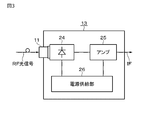
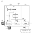
- FIG. 1 is a block diagram of an embodiment of the present technology.
- FIG. 2 is a block diagram showing a configuration for forming an input RF optical signal.
- FIG. 3 is a block diagram showing an example configuration of the photoelectric conversion unit.
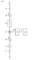
- FIG. 4 is a block diagram showing a configuration of an example of a tuner.
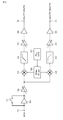
- FIG. 5 is a block diagram showing the configuration of another example of the tuner.
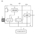
- FIG. 6 is a block diagram showing a configuration of a first modification of the embodiment of the present technology.
- FIG. 7 is a block diagram showing a configuration of a second modification of the embodiment of the present technology.
- FIG. 8 is a connection diagram for explaining the configuration of the switch unit in the second modification.
- FIG. 1 shows a first embodiment of the present technology
- 100 shows a high frequency receiver as a whole, which is the first embodiment.
- the high frequency receiver 100 is realized as a tuner module 100a and a demodulation module 100b.
- the tuner module may include a demodulator.
- the high frequency receiver 10 has an optical connector (optical signal input unit) 11 that can be connected to the POF line, and an electric signal input unit, for example, an F-type connector 12 that can be connected to a coaxial cable.
- the high-frequency receiver 10 is configured to include an optical-electric conversion unit 13, a switch unit 14, a tuner (for example, a satellite broadcast reception tuner, specifically a 4K tuner) 15, and a demodulation unit 16 in a metal shield case.
- the frequency at which antenna formation occurs due to internal wiring and frequency resonance of the case housing can be made higher than the reception frequency, so interference with mobile phones is also possible. Can be reduced.
- the antenna unit 21 includes an antenna that receives radio waves from satellites, a converter that converts the received signal of the antenna into an intermediate frequency and outputs it, and an intermediate frequency amplifier that amplifies the output of the converter.
- the converter converts the radio wave from the satellite into a 1st-IF signal having a frequency of right-handed 1032 MHz to 2071 MHz (left-handed 2224 to 3224 MHz).
- the 1st-IF signal of the output of the antenna unit 21 is hereinafter referred to as an RF electric signal.
- the RF electric signal is supplied to the electric light conversion unit 22, and the RF optical signal is taken out from the electric light conversion unit 22.
- This RF optical signal is supplied to the optical connector 11 of the high frequency receiver 100 through the POF 23 and the optical connector (not shown).
- the RF electric signal from the antenna unit 21 is supplied to the F-type connector 12 of the high-frequency receiver 100 via the coaxial cable and the connector.
- the output of the antenna unit 21 may be branched to take out the RF electric signal supplied to the F-type connector 12.
- the RF optical signal from the POF connector 11 is supplied to the optical / electrical conversion section 13, converted into the first RF electrical signal, and supplied to the switch section 14.
- a second RF electric signal from the F-type connector 12 is supplied to the switch unit 14.
- the switch unit 14 selectively outputs one of the two input RF electric signals.
- the RF electrical signal selected by the switch unit 14 is supplied to the tuner 15.
- the channel is selected by the tuner 15, the output (IF signal) of the tuner 15 is supplied to the demodulation unit 16, and the output of the demodulation unit 16 is supplied to the circuit of the television receiver.
- the high frequency receiver is provided in the television receiver.
- the RF optical signal from the optical connector 11 is converted into an electric signal by the photodiode light receiving element 24.
- the output of the photodiode light receiving element 24 is output as an RF electric signal via the RF amplifier 25, and is supplied to the switch unit 14. Power is supplied from the power supply unit 26 to the photodiode light receiving element 24 and the RF amplifier 25.
- the RF electric signal S21 connected by the switch unit 14 is supplied to the input terminal T1, and the IF signal is output from the output terminal T2.
- the RF electric signal is supplied to the mixer 33 via the low noise amplifier 31 and the RF variable amplifier 32 that amplifies or attenuates the RF electric signal S21.
- the output of the mixer 33 is supplied to the filter 34.
- the LO (local oscillation) signal from the VCO (Voltage Controlled Oscillator) 35 is supplied to the mixer 33.
- the VCO 35 is a frequency generator that generates an LO signal with a frequency of a specific channel.
- the PLL 37 is provided to set the frequency of the VCO 35 and keep it constant.
- the filter 34 selects the signal of the desired channel.
- the output signal of the filter 34 is taken out to the output terminal T2 via the IF variable amplifier 36.
- the configuration of the tuner 15 shown in FIG. 4 is an example, and may be configured to have a function of receiving terrestrial television broadcasting as well.
- the RF electric signal S21 connected by the switch unit 14 is supplied to the input terminal T3, and it is selected whether it is amplified by the LNA (Law Noise Amp) 50 or transmitted as it is by the switch 51, and is transmitted by the RF variable gain amplifier 52. After being amplified, it is divided into two and input to the I-axis mixer 53 and the Q-axis mixer 59.
- the local generation circuit 58 generates a local signal of PLL VCO 57, which is equal to the center frequency of the input signal, with a 90-degree phase shifter to generate a local signal whose phase is shifted and a local signal which is not shifted, and the two mixers 53 and 59.
- the configuration shown in FIG. 5 is an example of a configuration called an IQ detector or a Zero-IF tuner, which is a general circuit in a satellite broadcast receiver.
- the first embodiment of the present technology described above corresponds to both an RF optical signal and an RF electric signal, and can be electrically switched according to the distribution method without switching the wiring.
- the POF when the POF is wired, it is preferable to preferentially receive the RF optical signal from the viewpoint of radio wave leakage and the like.
- the RF electric signal has sufficient performance in all bands including 4K8K, or if the reception conditions are extremely poor due to rainfall conditions in the band to which satellite broadcasting is assigned, the RF optical signal is a signal.
- the quality information cannot be transmitted correctly, it is possible to switch to the reception of the RF electric signal and receive it, or to check the quality of the received signal.
- the housing can be made the same as the television receiver. Cost reduction is desired.
- the above-mentioned tuners and demodulators have been made into LSIs, and if the optoelectric conversion circuits are also made into LSIs and deployed on the same chip, further space saving and cost saving will be achieved. Will be done.
- the tuner 15 or the entire tuner 15 and the demodulation module 16 of the high-frequency receiver of the first embodiment of the present technology can be made into a size suitable for being incorporated in a metal shield case.
- the frequency at which the antenna is formed due to the frequency resonance of the internal wiring and the case housing can be made higher than the reception frequency, so that the interference of the leaked radio wave with the mobile phone can be suppressed.
- FIG. 6 shows the configuration of the high frequency receiver 101 (tuner module 101a and demodulation module 101b) as a modification of the first embodiment.
- a microcontroller 17 is provided, and each component of the high frequency receiving device 101 is connected by the system bus 18, and each component is controlled by the microcontroller 17 through the system bus 18. It is a thing.
- the microcontroller 17 determines the tuning frequency of the tuner 15 and sets the time constant of the AGC circuit of the tuner 15 to make settings suitable for digital demodulation of the demodulation unit 16.
- the microcontroller 17 also sets that the photoelectric conversion unit 13 optimizes the bias current of the photodiode light receiving element 24 (see FIG. 3) and causes the power supply unit 26 (see FIG. 3) to perform temperature compensation. be able to. Then, these software controls are performed by the microcontroller 17. These highly controlled receivers are compatible with the recent integration of functional components and control circuits that have been made into LSIs, miniaturization of large-scale circuits, and the like.
- the microcontroller 17 controls the switching of the switch unit 14 and switches between the RF electric signal converted from the RF optical signal and the RF electric signal from the F-type connector 12, thereby converting the high frequency receiver 101 into two signal formats. Can be made to correspond. That is, the switch unit 14 is controlled by the microcontroller 17 so as to detect the presence or absence of two RF electric signals and select the side of the existing RF electric signals. When two RF electric signals exist together, demodulation of the RF electric signal converted from the RF optical signal should be selected in order to suppress the leakage of radio waves that occurs when the RF electric signal is transmitted via the coaxial cable. Will be done.
- the switch unit 14 may be controlled so that the microcontroller 17 observes the bit error rate (BER) at the time of demodulation by the demodulation unit 16 and selects a better RF electric signal of the BER. Further, the switch unit 14 may be controlled by the modulation error rate (MER).
- BER bit error rate
- MER modulation error rate
- FIG. 7 shows the configuration of the high frequency receiver 102 (tuner module 102a and demodulation module 102b) as a further modification of the first embodiment.
- the microcontroller 17 is provided.
- the system bus 18A of the microcontroller 17 is connected only to the demodulation unit 16 of the high frequency receiver 102.
- a repeater function for relaying the system bus 18A to the system bus 18B in the module is built in, and the microcontroller 17 is connected to the system bus 18B via the demodulator 16.
- the microcontroller 17 can control the circuit connected to the system bus 18B.
- the high frequency receiver 102 is different from the high frequency receiver 101 shown in FIG. 6 in that the RF distributor 19, the detector 20, and the F type connector 41 are provided.
- the F-type connector 41 is provided to output an RF electric signal to an external device such as a recorder. Wiring can be simplified by providing the F-type connector 41.
- the RF distributor 19 inputs the output of the photoelectric converter 13 to the switch unit 40, and supplies a part of the output to the detector 20.
- the detector 20 transmits the output obtained by detecting the output level of the photoelectric converter 13 to the microcontroller 17 via the system bus 18B, the demodulation unit 16 and the system bus 18A.
- the switch unit 40 has switches SW1 and SW2 as schematically shown in FIG.
- the switches SW1 and SW2 are controlled by the control signals C1 and C2 supplied from the microcontroller 17 through the system bus 18B via the system bus 18B.
- the switch SW1 the RF electric signal from the RF distributor 19 is supplied to one input terminal 42a, and the RF electric signal from the F-type connector 12 is supplied to the other input terminal 42b.
- the output of switch SW1 is supplied to the input terminal of switch SW2.
- the RF electric signal taken out to one output terminal of the switch SW2 is input to the tuner 15, and the RF electric signal taken out to the other output terminal is input to the F type connector 41.
- the RF electrical signal output from the F-type connector 41 is not shown, it is supplied to the RF input of another device such as a recorder.
- the microcontroller 17 determines whether or not the output level of the photoelectric conversion unit 13 has reached a preset reference value, and controls the switch SW1 of the switch unit 40 according to the determination result.
- the switch SW1 is controlled to select the terminal 42a to which the output of the RF distributor 19 is supplied.
- the switch SW1 is controlled to select the terminal 42b to which the output of the F-type connector 12 is supplied. That is, the RF electric signal derived from the RF optical signal is preferentially selected.
- the switch SW1 may be controlled by referring to information indicating signal quality such as an AGC control signal in the tuner 15 and a bit error rate (BER) in the demodulation unit 16. Further, the switch unit 40 may be controlled by the modulation error rate (MER). Since it has the switch SW1 described above, it is possible to preferentially output an RF electric signal derived from an RF optical signal to other devices such as a television receiver and a recorder.
- information indicating signal quality such as an AGC control signal in the tuner 15 and a bit error rate (BER) in the demodulation unit 16.
- BER bit error rate
- the switch unit 40 may be controlled by the modulation error rate (MER). Since it is possible to preferentially output an RF electric signal derived from an RF optical signal to other devices such as a television receiver and a recorder.
- the RF electric signal selected by the switch SW1 is supplied to the switch SW2.
- the switch SW2 is controlled by the control signal C2 corresponding to the device selection.
- a device selection signal from an HDMI (registered trademark) (High-definition multimedia interface) controller is supplied to the microcontroller 17, and is controlled by a control signal C2 formed by the microcontroller 17.
- the RF electric signal selected by the switch SW1 is supplied to the tuner 15.
- the signal selected by the tuner 15 is demodulated by the demodulation unit 16.
- the RF electric signal selected by the switch SW1 is supplied to the F-type connector 41.
- the optical connector as the optical signal input unit and the F-type high frequency receiver 12 as the electric signal input unit are provided, either the optical signal or the electric signal is provided for the room. If the connection portion of is provided, it is possible to receive the television RF signal. Further, since the optical-electric conversion unit is provided in the shield case, it is possible to suppress the problem that the electric signal (radio wave) converted from the optical signal leaks and interferes with the mobile phone.
- the present invention is not limited to the above-described embodiments, and various modifications based on the technical idea of the present technology are possible. For example, various modifications as described below are possible. In addition, one or a plurality of arbitrarily selected modifications may be appropriately combined in the following modification modes. In addition, the configurations, methods, processes, shapes, materials, numerical values, and the like of the above-described embodiments can be combined with each other as long as they do not deviate from the gist of the present technology. For example, a connector other than the F-type connector may be used as the input unit for the RF electric signal.
- the present technology can also adopt the following configurations.
- a high-frequency receiver in which the photoelectric conversion unit, the switch unit, and the tuner are housed in the same housing.
- the high frequency reception according to any one of (1) to (6) which has a detector that detects the output from the photoelectric conversion unit and is equipped with a microcontroller that controls the switch unit according to the output of the detector.
- Device. (8) The high-frequency receiver according to any one of (1) to (7), which has an output terminal for outputting an output signal of the switch unit.
Landscapes
- Engineering & Computer Science (AREA)
- Computer Networks & Wireless Communication (AREA)
- Signal Processing (AREA)
- Physics & Mathematics (AREA)
- Electromagnetism (AREA)
- Input Circuits Of Receivers And Coupling Of Receivers And Audio Equipment (AREA)
- Circuits Of Receivers In General (AREA)
Abstract
RF光信号が入力される光信号入力部と、光入力部から入力されたRF光信号を第1のRF電気信号に変換する光電気変換部と、第2のRF電気信号が入力される電気信号入力部と、第1のRF電気信号と第2のRF電気信号を択一的に選択するスイッチ部と、スイッチ部に接続され、周波数選択するチューナーとを備え、光電気変換部とスイッチ部とチューナーが同一の筐体内に収納された高周波受信装置である。 図1
Description
本技術は、高周波受信装置に関する。
2018年12月1日からわが国において新4K8K衛星放送が開始されている。新4K8K衛星放送の左旋で使用するアンテナ出力周波数帯(2224~3224MHz)において、同一周波数帯で既にサービスを実施している他の無線システムには、移動通信、ISMバンド、各種レーダー等が運用されている。適切な高周波受信装置を使用し、正しく施工すれば問題が生じないが、電波の漏洩を遮へいする性能が低い機器では、相互に電波干渉を引き起こす可能性がある。
他の無線サービスへの電波干渉を生じないように、衛星放送の周波数帯域における漏洩電力を所定値以下とする規則が制定されている。しかしながら、この値は現在普及している携帯電話(スマートフォン)の実効的な受信感度に比べて非常に大きく、携帯電話の使用する周波数帯域で電波漏洩が起きると、携帯電話の通信や通話に重大な影響を与えかねない。
特許文献1には、このような問題を考慮してプラスチック光ファイバ(POF(Plastic Optical Fiber))によって家庭内のテレビジョン(RF)配線を置き換えて電波の漏洩を減ずることが提案されている。POFは、折れないで曲げやすい特性を有している。また、特許文献2には、端末機器の背面にアタッチメントもしくは内部に内蔵するだけの超小型化および超低消費電力化を低コストで実現できる光受信装置について記載されている。
特許文献1の図2の構成では、光受信機21からTV-RF信号が出力され、同軸線路コネクタ27及び同軸線路29を介してTVによって受信される。したがって、光受信機21とTV(4Kチューナー)の間の同軸線路29から電波漏洩か生じる可能性があった。この漏洩を阻止するためには、同軸線路29として非常に高価な高シールド効果を持つ厳重なグランド被覆によって覆われた同軸線路等の使用が必要になる。
また、特許文献2には、RF多重信号が重畳された光信号を入力する光受信部と、光受信部から出力されるRF多重電気信号を出力するF型コネクタを筐体に設けた受信装置が記載されている。しかしながら、従来の同軸ケーブルの配線が上述したPOFによる配線網に直ぐに置き換わるとはいえず、両方の伝送システムが併存する可能性がある。このような状況では、特許文献2に記載されているように、光入力のみを有する構成は、汎用性に乏しい問題がある。
したがって、本技術は、これらの問題を解決するようにした高周波受信装置の提供を目的とする。
本技術は、RF光信号が入力される光信号入力部と、
光入力部から入力されたRF光信号を第1のRF電気信号に変換する光電気変換部と、
第2のRF電気信号が入力される電気信号入力部と、
第1のRF電気信号と第2のRF電気信号を択一的に選択するスイッチ部と、
スイッチ部に接続され、周波数選択するチューナーとを備え、
光電気変換部とスイッチ部とチューナーが同一の筐体内に収納された高周波受信装置である。
光入力部から入力されたRF光信号を第1のRF電気信号に変換する光電気変換部と、
第2のRF電気信号が入力される電気信号入力部と、
第1のRF電気信号と第2のRF電気信号を択一的に選択するスイッチ部と、
スイッチ部に接続され、周波数選択するチューナーとを備え、
光電気変換部とスイッチ部とチューナーが同一の筐体内に収納された高周波受信装置である。
以下に説明する実施形態は、本技術の好適な具体例であり、技術的に好ましい種々の限定が付されている。しかしながら、本技術の範囲は、以下の説明において、特に本技術を限定する旨の記載がない限り、これらの実施形態に限定されないものとする。また、以下の説明において、同一の名称、符号については同一もしくは同質の構成要素を示しており、重複する説明を適宜省略する。
図1は、本技術の第1の実施形態を示し、100が第1の実施形態である高周波受信装置を全体として示す。高周波受信装置100は、チューナーモジュール100a及び復調モジュール100bとして実現される。チューナーモジュールに復調部が含まれるようにしてもよい。なお、以下の説明では、衛星テレビジョン放送、特に4K放送を受信する場合に対して本技術を適用した例について説明する。
POFラインと接続可能とされた光コネクタ(光信号入力部)11と、同軸ケーブルと接続可能とされた電気信号入力部例えばF型コネクタ12を高周波受信装置10が有する。高周波受信装置10は、金属のシールドケース内に光電気変換部13、スイッチ部14及びチューナー(例えば衛星放送受信チューナー、具体的には4Kチューナー)15及び復調部16が設けられた構成とされている。金属のシールドケースに内蔵する事に適したサイズのモジュールにおいては内部の配線やケース筐体の周波数共振によるアンテナ化が起こる周波数を当該受信周波数よりも高くできるので、携帯電話への干渉も同様に減ずることができる。
図2に示すように、アンテナ部21では、衛星からの電波を受信するアンテナと、アンテナの受信信号を中間周波数に変換して出力するコンバーターと、コンバーターの出力を増幅する中間周波アンプを有する。コンバーターは、衛星からの電波を右旋1032MHz~2071MHz(左旋2224~3224MHz)の周波数の1st-IF信号に変換する。アンテナ部21の出力の1st-IF信号を以下ではRF電気信号と称する。
RF電気信号が電気光変換部22に供給され、電気光変換部22からRF光信号が取り出される。このRF光信号がPOF23及び光コネクタ(図示せず)を通じて高周波受信装置100の光コネクタ11に供給される。既存の住宅などでPOFの配線がされていない場合には、アンテナ部21からのRF電気信号が同軸ケーブル及びコネクタを介して高周波受信装置100のF型コネクタ12に供給される。なお、アンテナ部21の出力を分岐してF型コネクタ12に供給されるRF電気信号を取り出すようにしてもよい。
POFコネクタ11からのRF光信号が光電気変換部路13に供給され、第1のRF電気信号に変換され、スイッチ部14に対して供給される。F型コネクタ12からの第2のRF電気信号がスイッチ部14に対して供給される。スイッチ部14は、入力された二つのRF電気信号の一方を択一的に出力する。スイッチ部14によって選択されたRF電気信号がチューナー15に対して供給される。チューナー15で選局されてチューナー15の出力(IF信号)が復調部16に供給され、復調部16の出力がテレビジョン受信機の回路に対して供給される。なお、高周波受信装置は、テレビジョン受像機内に設けられている。
光電気変換部13の一例について図3を参照して説明する。光コネクタ11からのRF光信号がフォトダイオード受光素子24によって電気信号に変換される。フォトダイオード受光素子24の出力がRFアンプ25を介してRF電気信号として出力され、スイッチ部14に対して供給される。フォトダイオード受光素子24及びRFアンプ25に対しては、電源供給部26からの電源が供給される。
チューナー15の一例を図4に示す。スイッチ部14によって接続されたRF電気信号S21が入力端子T1に供給され、出力端子T2からIF信号が出力される。RF電気信号がローノイズアンプ31、RF電気信号S21を増幅又は減衰するRF可変増幅器32を介して混合器33に供給される。混合器33の出力がフィルタ34に供給される。
混合器33に対してVCO(Voltage Controlled Oscillator)35からのLO(局部発振)信号が供給される。VCO35は、特定のチャンネルの周波数のLO信号を発生する周波数発生器である。VCO35の周波数を設定して一定に保つためにPLL37が設けられている。フィルタ34によって、所望のチャンネルの信号が選択される。フィルタ34の出力信号がIF可変アンプ36を介して出力端子T2に取り出される。なお、図4に示すチューナー15の構成は一例であって、地上波テレビ放送も受信する機能を有する構成であってもよい。
チューナー15の他の例について図5を使って説明する。スイッチ部14によって接続されたRF電気信号S21が入力端子T3に供給され、LNA(Law Noise Amp) 50にて増幅されるか、スイッチ51によってそのまま伝送されるか選択され、RF可変ゲインアンプ52で増幅された後、2分配されてI軸ミキサー53とQ軸ミキサー59に入力されル。ローカル生成回路58によって、当該入力信号の中心周波数と等しいPLL VCO57のローカル信号を90度移相器にて位相をずらしたローカルとずらさないローカルとを生成させて前記二つのミキサー53、59にて検波し、ベースバンド信号を得る。こうして得られたI軸及びQ軸のベースバンド信号はそれぞれLPF54及び60にて高域周波数を減衰させられ、ベースバンドの可変ゲインアンプ55及び61にて前記復調部16の入力に適した振幅に整えバッファーアンプ56及び62を介してI軸出力端子T4とQ軸出力端子T5に出力される。図5に示す構成はIQ検波器或いはZero-IFチューナーと呼ばれる構成例であり、衛星放送の受信機において一般的な回路である。
上述した本技術の第1の実施形態は、RF光信号及びRF電気信号の両者に対応しており、その配信方法に応じて配線の切り替えをせずに電気的にスイッチすることができる。一般にPOFが配線されている場合には、RF光信号を優先的に受信する方が電波の漏洩等の見地では望ましい。しかしながら、4K8Kを含む全ての帯域でRF電気信号が充分な性能であるか、あるいは、衛星放送が割り当てられている帯域では降雨の状況などで受信条件が極めて悪い場合において、RF光信号が信号の品質情報を正しく伝送できない時には、RF電気信号の受信に切り替えて受信したり、受信信号の品質を確認したりすることができる。
さらに、従来のテレビジョン光伝送受信機に比べて小型にすることができるので、テレビジョン受信機などの機器に内蔵することができ、筐体をテレビジョン受信機と同一にすることができるので省コスト化が望まれる。また、昨今では前述のチューナーや復調器はLSI化が進んでおり、当該光電気変換回路もLSI化され同一のチップ上に展開されることになれば一段の省スペース化、省コスト化が達成される。
また、本技術の第1の実施形態の高周波受信装置のチューナー15或いはチューナー15及び復調モジュール16の全体を金属のシールドケースに内蔵するのに適したサイズにすることができる。小型化されたモジュールにおいては内部の配線やケース筐体の周波数共振によるアンテナ化が起こる周波数を当該受信周波数よりも高くできるので、漏洩電波の携帯電話への干渉を抑圧することができる。
さらに、本技術と異なり、光信号の入力端子しか備えていない場合には、RF電気信号が出力されるコネクタに対して接続することができない不都合が生じる。既存の住宅、集合住宅などで、POF配線がされていない場合には、RF電気信号をRF光信号に変換する電気光変換装置を別個に用意してその出力を光コネクタに供給する必要が生じ、電波漏洩のおそれが生じたり、電気光変換装置を用意するために余計な出費が生じる(電源なども必要とされ、消費電力の増加する)。本技術によれば、RF光信号の入力端子(光コネクタ11)及びRF電気信号の入力端子(F型コネクタ12)の両方を備えているので、上述したような問題を回避することができる。
図6は、第1の実施形態の変形例としての高周波受信装置101(チューナーモジュール101a及び復調モジュール101b)の構成を示す。図1の構成と比較すると、マイクロコントローラ17が設けられており、高周波受信装置101の各構成要素をシステムバス18で接続し、システムバス18を通じて各構成要素をマイクロコントローラ17によって制御するようにしたものである。マイクロコントローラ17は、チューナー15の選局周波数を決定したり、チューナー15のAGC回路の時定数を設定したりして、復調部16のデジタル復調に適した設定を行なう。
マイクロコントローラ17は、さらに、光電気変換部13において、フォトダイオード受光素子24(図3参照)のバイアス電流の最適化、温度補償を電源供給部26(図3参照)に行なわせるなども設定することができる。そして、これらのソフトウェア制御がマイクロコントローラ17によってなされる。これらの高度制御型受信機は、最近のLSI化された機能部品と制御回路の集積化、大規模回路の小型化等の面と相性が良い。
さらに、マイクロコントローラ17は、スイッチ部14の切替を制御し、RF光信号を変換したRF電気信号と、F型コネクタ12からのRF電気信号を切り替えることによって、二つの信号形式に高周波受信装置101を対応させることができる。すなわち、二つのRF電気信号の有無を検出して存在しているRF電気信号の側を選択するように、スイッチ部14がマイクロコントローラ17によって制御される。二つのRF電気信号が共に存在する場合には、RF電気信号を同軸ケーブルを介して伝送する時に起きる電波の漏洩を抑制するために、RF光信号を変換したRF電気信号の復調を選択するようになされる。なお、マイクロコントローラ17が復調部16による復調時のビットエラーレート(BER)を観測し、BERのより良いRF電気信号を選択するように、スイッチ部14を制御してもよい。さらに、モジュレーションエラーレート(MER)によってスイッチ部14を制御するようにしてもよい。
図7は、第1の実施形態のさらなる変形例としての高周波受信装置102(チューナーモジュール102a及び復調モジュール102b)の構成を示す。図6の高周波受信装置101の構成と同様に、マイクロコントローラ17が備えられている。高周波受信装置102の復調部16のみに、マイクロコントローラ17のシステムバス18Aが接続されている。復調部16の内部には、システムバス18Aをモジュール内のシステムバス18Bに中継するリピーターの機能が内蔵されており、マイクロコントローラ17は、復調部16を介してシステムバス18Bに接続されており、システムバス18Bに接続されている回路をマイクロコントローラ17が制御することができる。
高周波受信装置102は、図6に示す高周波受信装置101と比較すると、RF分配器19と検波器20とF型コネクタ41が設けられている点で相違している。F型コネクタ41は、RF電気信号を外部例えばレコーダに対して出力するために設けられている。F型コネクタ41を設けることによって、配線を簡単とすることができる。RF分配器19は、光電気変換器13の出力をスイッチ部40に対して入力すると共に、その一部を検波器20に対して供給する。検波器20は、光電気変換器13の出力レベルを検波した出力をシステムバス18B、復調部16及びシステムバス18Aを介してマイクロコントローラ17に伝達する。
スイッチ部40は、図8に模式的に示すように、スイッチSW1及びSW2を有する。スイッチSW1及びSW2は、システムバス18Bを介してマイクロコントローラ17からシステムバス18Bを通じて供給される制御信号C1及びC2によって制御される。スイッチSW1は、一方の入力端子42aに対してRF分配器19からのRF電気信号が供給され、他方の入力端子42bに対してF型コネクタ12からのRF電気信号が供給される。
スイッチSW1の出力がスイッチSW2の入力端子に供給される。スイッチSW2の一方の出力端子に取り出されたRF電気信号がチューナー15に対して入力され、その他方の出力端子に取り出されたRF電気信号がF型コネクタ41に対して入力される。F型コネクタ41から出力されるRF電気信号が図示しないが、他の機器例えばレコーダのRF入力に対して供給される。
マイクロコントローラ17は、光電気変換部13の出力レベルが予め設定した基準値に達しているかどうかを判定し、判定結果に応じてスイッチ部40のスイッチSW1を制御する。出力レベルが基準値に達していると判定された場合には、スイッチSW1がRF分配器19の出力が供給される端子42aを選択するように制御される。逆に出力レベルが基準値に達していないと判定された場合には、スイッチSW1がF型コネクタ12の出力が供給される端子42bを選択するように制御される。すなわち、RF光信号から派生したRF電気信号が優先的に選択される。なお、RF電気信号のレベル以外に、チューナー15におけるAGC制御信号、復調部16におけるビットエラーレート(BER)などの信号品質を表す情報を参照してスイッチSW1を制御するようにしてもよい。さらに、モジュレーションエラーレート(MER)によってスイッチ部40を制御するようにしてもよい。上述したスイッチSW1を有するので、テレビジョン受像機及びレコーダなどの他の機器に対してRF光信号由来のRF電気信号を優先して出力することができる。
スイッチSW1によって選択されたRF電気信号がスイッチSW2に対して供給される。スイッチSW2は、機器選択に対応する制御信号C2によって制御される。例えばHDMI(登録商標)(High-definition multimedia interface)コントローラからの機器選択信号がマイクロコントローラ17に供給され、マイクロコントローラ17によって形成された制御信号C2によって制御される。テレビジョン受像機を選択する機器選択信号が形成される場合には、スイッチSW1によって選択されたRF電気信号がチューナー15に供給される。チューナー15で選局した信号が復調部16で復調される。レコーダを選択する機器選択信号が形成される場合には、スイッチSW1によって選択されたRF電気信号がF型コネクタ41に供給される。
上述した本技術の実施形態によれば、光信号入力部としての光コネクタと電気信号入力部としてのF型高周波受信装置12を備えているので、部屋に対して光信号と電気信号のいずれかの接続部が設けられていれば、テレビジョンRF信号を受信することが可能となる。また、光電気変換部がシールドケース内に設けられているので、光信号を変換した電気信号(電波)が漏洩して携帯電話の妨害となるような問題を抑えることができる。
以上、本技術の実施形態について具体的に説明したが、上述の各実施形態に限定されるものではなく、本技術の技術的思想に基づく各種の変形が可能である。例えば次に述べるような各種の変形が可能である。また、次に述べる変形の態様は、任意に選択された一または複数を、適宜に組み合わせることもできる。また、上述の実施形態の構成、方法、工程、形状、材料および数値などは、本技術の主旨を逸脱しない限り、互いに組み合わせることが可能である。例えばRF電気信号の入力部としてはF型コネクタ以外のコネクタを使用してもよい。
なお、本技術は、以下のような構成も採ることができる。
(1)
RF光信号が入力される光信号入力部と、
前記光入力部から入力されたRF光信号を第1のRF電気信号に変換する光電気変換部と、
第2のRF電気信号が入力される電気信号入力部と、
前記第1のRF電気信号と前記第2のRF電気信号を択一的に選択するスイッチ部と、
前記スイッチ部に接続され、周波数選択するチューナーとを備え、
前記光電気変換部と前記スイッチ部と前記チューナーが同一の筐体内に収納された高周波受信装置。
(2)
前記筐体がシールドケースである請求項1に記載の高周波受信装置。
(3)
前記スイッチ部は、前記第1及び第2のRF電気信号が共に存在する場合に、優先的に前記第1のRF電気信号を選択するようになされた(1)又は(2)に記載の高周波受信装置。
(4)
前記チューナーによって周波数選択された信号を復調する復調部を有する(1)から(3)の何れかに記載の高周波受信装置。
(5)
前記復調部がシールドケース内に収納された(4)に記載の高周波受信装置。
(6)
信号レベルまたは復調された信号の品位によって、前記スイッチ部を制御するマイクロコントローラを備えた(1)から(5)の何れかに記載の光高周波受信装置。
(7)
光電気変換部からの出力を検波する検波器を有し、前記検波器の出力に応じて前記スイッチ部を制御するマイクロコントローラを備えた(1)から(6)の何れかに記載の高周波受信装置。
(8)
前記スイッチ部の出力信号を出力する出力端子を有する(1)から(7)の何れかに記載の高周波受信装置。
(1)
RF光信号が入力される光信号入力部と、
前記光入力部から入力されたRF光信号を第1のRF電気信号に変換する光電気変換部と、
第2のRF電気信号が入力される電気信号入力部と、
前記第1のRF電気信号と前記第2のRF電気信号を択一的に選択するスイッチ部と、
前記スイッチ部に接続され、周波数選択するチューナーとを備え、
前記光電気変換部と前記スイッチ部と前記チューナーが同一の筐体内に収納された高周波受信装置。
(2)
前記筐体がシールドケースである請求項1に記載の高周波受信装置。
(3)
前記スイッチ部は、前記第1及び第2のRF電気信号が共に存在する場合に、優先的に前記第1のRF電気信号を選択するようになされた(1)又は(2)に記載の高周波受信装置。
(4)
前記チューナーによって周波数選択された信号を復調する復調部を有する(1)から(3)の何れかに記載の高周波受信装置。
(5)
前記復調部がシールドケース内に収納された(4)に記載の高周波受信装置。
(6)
信号レベルまたは復調された信号の品位によって、前記スイッチ部を制御するマイクロコントローラを備えた(1)から(5)の何れかに記載の光高周波受信装置。
(7)
光電気変換部からの出力を検波する検波器を有し、前記検波器の出力に応じて前記スイッチ部を制御するマイクロコントローラを備えた(1)から(6)の何れかに記載の高周波受信装置。
(8)
前記スイッチ部の出力信号を出力する出力端子を有する(1)から(7)の何れかに記載の高周波受信装置。
11・・・光コネクタ、12・・・F型コネクタ
13・・・光電気変換部、14・・・スイッチ部
15・・・チューナー、16・・・復調部
17・・・マイクロコントローラ、19・・・RF分配器
40・・・スイッチ部、41・・・F型コネクタ
13・・・光電気変換部、14・・・スイッチ部
15・・・チューナー、16・・・復調部
17・・・マイクロコントローラ、19・・・RF分配器
40・・・スイッチ部、41・・・F型コネクタ
Claims (8)
- RF光信号が入力される光信号入力部と、
前記光入力部から入力されたRF光信号を第1のRF電気信号に変換する光電気変換部と、
第2のRF電気信号が入力される電気信号入力部と、
前記第1のRF電気信号と前記第2のRF電気信号を択一的に選択するスイッチ部と、
前記スイッチ部に接続され、周波数選択するチューナーとを備え、
前記光電気変換部と前記スイッチ部と前記チューナーが同一の筐体シールドケース内に収納された高周波受信装置。 - 前記筐体がシールドケースである請求項1に記載の高周波受信装置。
- 前記スイッチ部は、前記第1及び第2のRF電気信号が共に存在する場合に、優先的に前記第1のRF電気信号を選択するようになされた請求項1に記載の高周波受信装置。
- 前記チューナーによって周波数選択された信号を復調する復調部を有する請求項1に記載の高周波受信装置。
- 前記復調部がシールドケース内に収納された請求項4に記載の高周波受信装置。
- 信号レベルまたは復調された信号の品位によって、前記スイッチ部を制御するマイクロコントローラを備えた請求項1に記載の光高周波受信装置。
- 光電気変換部からの出力を検波する検波器を有し、前記検波器の出力に応じて前記スイッチ部を制御するマイクロコントローラを備えた請求項1に記載の高周波受信装置。
- 前記スイッチ部の出力信号を出力する出力端子を有する請求項1に記載の高周波受信装置。
Priority Applications (1)
| Application Number | Priority Date | Filing Date | Title |
|---|---|---|---|
| JP2022505833A JP7666842B2 (ja) | 2020-03-10 | 2021-02-03 | 高周波受信装置 |
Applications Claiming Priority (2)
| Application Number | Priority Date | Filing Date | Title |
|---|---|---|---|
| JP2020-040992 | 2020-03-10 | ||
| JP2020040992 | 2020-03-10 |
Publications (1)
| Publication Number | Publication Date |
|---|---|
| WO2021181954A1 true WO2021181954A1 (ja) | 2021-09-16 |
Family
ID=77671406
Family Applications (1)
| Application Number | Title | Priority Date | Filing Date |
|---|---|---|---|
| PCT/JP2021/003922 Ceased WO2021181954A1 (ja) | 2020-03-10 | 2021-02-03 | 高周波受信装置 |
Country Status (2)
| Country | Link |
|---|---|
| JP (1) | JP7666842B2 (ja) |
| WO (1) | WO2021181954A1 (ja) |
Citations (3)
| Publication number | Priority date | Publication date | Assignee | Title |
|---|---|---|---|---|
| JPH05235864A (ja) * | 1992-02-24 | 1993-09-10 | Matsushita Electric Ind Co Ltd | 自動伝送路切り換え装置 |
| JP2001268530A (ja) * | 2000-03-17 | 2001-09-28 | Sharp Corp | Catv用チューナ |
| JP2018033065A (ja) * | 2016-08-26 | 2018-03-01 | Dxアンテナ株式会社 | 広帯域ハイブリッド共同受信システム及び光受信機(v−onu) |
-
2021
- 2021-02-03 JP JP2022505833A patent/JP7666842B2/ja active Active
- 2021-02-03 WO PCT/JP2021/003922 patent/WO2021181954A1/ja not_active Ceased
Patent Citations (3)
| Publication number | Priority date | Publication date | Assignee | Title |
|---|---|---|---|---|
| JPH05235864A (ja) * | 1992-02-24 | 1993-09-10 | Matsushita Electric Ind Co Ltd | 自動伝送路切り換え装置 |
| JP2001268530A (ja) * | 2000-03-17 | 2001-09-28 | Sharp Corp | Catv用チューナ |
| JP2018033065A (ja) * | 2016-08-26 | 2018-03-01 | Dxアンテナ株式会社 | 広帯域ハイブリッド共同受信システム及び光受信機(v−onu) |
Also Published As
| Publication number | Publication date |
|---|---|
| JP7666842B2 (ja) | 2025-04-22 |
| JPWO2021181954A1 (ja) | 2021-09-16 |
Similar Documents
| Publication | Publication Date | Title |
|---|---|---|
| JP3889885B2 (ja) | ミリ波送信装置、ミリ波受信装置、ミリ波送受信システム及び電子機器 | |
| JP3753518B2 (ja) | ケーブルモデム用チューナ | |
| US5530929A (en) | Homodyne receiver minimizing oscillator leakage | |
| AU742379B2 (en) | Apparatus and method for processing signals selected from multiple data streams | |
| EP1863193B1 (en) | Digital satellite receiver and method for switching among multiple receiver antennas using diversity circuitry | |
| US20070184804A1 (en) | Method and device for cancelling interferences | |
| CN108055049B (zh) | 无线数传电台接收电路 | |
| US9374181B2 (en) | Mobile terminal and method for receiving and transmitting radio frequency signal | |
| JP4639809B2 (ja) | 電子チューナとこれを用いた携帯機器 | |
| US20060150219A1 (en) | Satellite digital multimedia broadcasting receiver of single tuning type | |
| US20060053453A1 (en) | Wireless redistribution system for terrestrial digital television broadcasting and receiving system for terrestrial digital television broadcasting | |
| CN101505158A (zh) | 能防止地面波广播和卫星广播的相互干扰的复合调谐器 | |
| US9516256B2 (en) | Apparatus and method for processing a radio frequency signal | |
| US7489899B2 (en) | Information network building method and network connection circuit for communication between terminals of a physical premises | |
| JP7666842B2 (ja) | 高周波受信装置 | |
| JP2010130328A (ja) | テレビジョン放送受信回路 | |
| KR100667151B1 (ko) | 직접변환 방식을 이용한 디지털 초협대역 단말 시스템 및그의 다중대역 송수신 장치 | |
| JP5092282B2 (ja) | 受信装置 | |
| JP4681332B2 (ja) | 送受信システム及び受信装置 | |
| US7447489B2 (en) | Digital tuner | |
| US10673480B2 (en) | Device for transmitting and receiving mobile radio signals by means of a stationary antenna | |
| JP4346534B2 (ja) | チューナ装置 | |
| JP3919713B2 (ja) | ミリ波信号分配中継器、ミリ波送受信システム及び電子機器 | |
| JP6257284B2 (ja) | 受信装置 | |
| JP4407017B2 (ja) | 無線通信機器 |
Legal Events
| Date | Code | Title | Description |
|---|---|---|---|
| 121 | Ep: the epo has been informed by wipo that ep was designated in this application |
Ref document number: 21768212 Country of ref document: EP Kind code of ref document: A1 |
|
| ENP | Entry into the national phase |
Ref document number: 2022505833 Country of ref document: JP Kind code of ref document: A |
|
| NENP | Non-entry into the national phase |
Ref country code: DE |
|
| 122 | Ep: pct application non-entry in european phase |
Ref document number: 21768212 Country of ref document: EP Kind code of ref document: A1 |