WO2021181882A1 - 撮像装置及び撮像方法 - Google Patents
撮像装置及び撮像方法 Download PDFInfo
- Publication number
- WO2021181882A1 WO2021181882A1 PCT/JP2021/001497 JP2021001497W WO2021181882A1 WO 2021181882 A1 WO2021181882 A1 WO 2021181882A1 JP 2021001497 W JP2021001497 W JP 2021001497W WO 2021181882 A1 WO2021181882 A1 WO 2021181882A1
- Authority
- WO
- WIPO (PCT)
- Prior art keywords
- region
- interest
- pixel
- signal
- unit
- Prior art date
- Legal status (The legal status is an assumption and is not a legal conclusion. Google has not performed a legal analysis and makes no representation as to the accuracy of the status listed.)
- Ceased
Links
Images






Classifications
-
- H—ELECTRICITY
- H04—ELECTRIC COMMUNICATION TECHNIQUE
- H04N—PICTORIAL COMMUNICATION, e.g. TELEVISION
- H04N25/00—Circuitry of solid-state image sensors [SSIS]; Control thereof
- H04N25/40—Extracting pixel data from image sensors by controlling scanning circuits, e.g. by modifying the number of pixels sampled or to be sampled
- H04N25/42—Extracting pixel data from image sensors by controlling scanning circuits, e.g. by modifying the number of pixels sampled or to be sampled by switching between different modes of operation using different resolutions or aspect ratios, e.g. switching between interlaced and non-interlaced mode
-
- H—ELECTRICITY
- H04—ELECTRIC COMMUNICATION TECHNIQUE
- H04N—PICTORIAL COMMUNICATION, e.g. TELEVISION
- H04N25/00—Circuitry of solid-state image sensors [SSIS]; Control thereof
- H04N25/40—Extracting pixel data from image sensors by controlling scanning circuits, e.g. by modifying the number of pixels sampled or to be sampled
- H04N25/44—Extracting pixel data from image sensors by controlling scanning circuits, e.g. by modifying the number of pixels sampled or to be sampled by partially reading an SSIS array
- H04N25/443—Extracting pixel data from image sensors by controlling scanning circuits, e.g. by modifying the number of pixels sampled or to be sampled by partially reading an SSIS array by reading pixels from selected two-dimensional [2D] regions of the array, e.g. for windowing or digital zooming
-
- G—PHYSICS
- G01—MEASURING; TESTING
- G01C—MEASURING DISTANCES, LEVELS OR BEARINGS; SURVEYING; NAVIGATION; GYROSCOPIC INSTRUMENTS; PHOTOGRAMMETRY OR VIDEOGRAMMETRY
- G01C3/00—Measuring distances in line of sight; Optical rangefinders
- G01C3/02—Details
- G01C3/06—Use of electric means to obtain final indication
-
- G—PHYSICS
- G01—MEASURING; TESTING
- G01S—RADIO DIRECTION-FINDING; RADIO NAVIGATION; DETERMINING DISTANCE OR VELOCITY BY USE OF RADIO WAVES; LOCATING OR PRESENCE-DETECTING BY USE OF THE REFLECTION OR RERADIATION OF RADIO WAVES; ANALOGOUS ARRANGEMENTS USING OTHER WAVES
- G01S17/00—Systems using the reflection or reradiation of electromagnetic waves other than radio waves, e.g. lidar systems
- G01S17/88—Lidar systems specially adapted for specific applications
- G01S17/89—Lidar systems specially adapted for specific applications for mapping or imaging
- G01S17/894—Three-dimensional [3D] imaging with simultaneous measurement of time-of-flight at a two-dimensional [2D] array of receiver pixels, e.g. time-of-flight cameras or flash lidar
-
- G—PHYSICS
- G01—MEASURING; TESTING
- G01S—RADIO DIRECTION-FINDING; RADIO NAVIGATION; DETERMINING DISTANCE OR VELOCITY BY USE OF RADIO WAVES; LOCATING OR PRESENCE-DETECTING BY USE OF THE REFLECTION OR RERADIATION OF RADIO WAVES; ANALOGOUS ARRANGEMENTS USING OTHER WAVES
- G01S7/00—Details of systems according to groups G01S13/00, G01S15/00, G01S17/00
- G01S7/48—Details of systems according to groups G01S13/00, G01S15/00, G01S17/00 of systems according to group G01S17/00
- G01S7/491—Details of non-pulse systems
- G01S7/4912—Receivers
- G01S7/4913—Circuits for detection, sampling, integration or read-out
- G01S7/4914—Circuits for detection, sampling, integration or read-out of detector arrays, e.g. charge-transfer gates
-
- H—ELECTRICITY
- H04—ELECTRIC COMMUNICATION TECHNIQUE
- H04N—PICTORIAL COMMUNICATION, e.g. TELEVISION
- H04N25/00—Circuitry of solid-state image sensors [SSIS]; Control thereof
- H04N25/40—Extracting pixel data from image sensors by controlling scanning circuits, e.g. by modifying the number of pixels sampled or to be sampled
-
- H—ELECTRICITY
- H04—ELECTRIC COMMUNICATION TECHNIQUE
- H04N—PICTORIAL COMMUNICATION, e.g. TELEVISION
- H04N25/00—Circuitry of solid-state image sensors [SSIS]; Control thereof
- H04N25/50—Control of the SSIS exposure
- H04N25/53—Control of the integration time
-
- H—ELECTRICITY
- H04—ELECTRIC COMMUNICATION TECHNIQUE
- H04N—PICTORIAL COMMUNICATION, e.g. TELEVISION
- H04N25/00—Circuitry of solid-state image sensors [SSIS]; Control thereof
- H04N25/70—SSIS architectures; Circuits associated therewith
- H04N25/76—Addressed sensors, e.g. MOS or CMOS sensors
- H04N25/77—Pixel circuitry, e.g. memories, A/D converters, pixel amplifiers, shared circuits or shared components
- H04N25/772—Pixel circuitry, e.g. memories, A/D converters, pixel amplifiers, shared circuits or shared components comprising A/D, V/T, V/F, I/T or I/F converters
-
- G—PHYSICS
- G01—MEASURING; TESTING
- G01S—RADIO DIRECTION-FINDING; RADIO NAVIGATION; DETERMINING DISTANCE OR VELOCITY BY USE OF RADIO WAVES; LOCATING OR PRESENCE-DETECTING BY USE OF THE REFLECTION OR RERADIATION OF RADIO WAVES; ANALOGOUS ARRANGEMENTS USING OTHER WAVES
- G01S17/00—Systems using the reflection or reradiation of electromagnetic waves other than radio waves, e.g. lidar systems
- G01S17/02—Systems using the reflection of electromagnetic waves other than radio waves
- G01S17/06—Systems determining position data of a target
- G01S17/08—Systems determining position data of a target for measuring distance only
Definitions
- the technique according to the present disclosure (the present technique) relates to an imaging device and an imaging method used in a distance measuring device.
- the direct ToF (dToF) method that measures the distance from the optical flight time that is directly measured using pulse waves.
- a distance measuring device and an indirect ToF (iToF) type distance measuring device that measures a distance from an optical flight time indirectly calculated by using the phase of a modulated light are known.
- the iToF type distance measuring device light is irradiated from a light source, the light reflected by the object is received by the light receiving element, and the photoelectric conversion unit in the light receiving element performs photoelectric conversion. The charges generated by the photoelectric conversion unit are distributed to the plurality of charge storage units by the plurality of transfer transistors. Then, the distance to the object is calculated based on the phase signal corresponding to the amount of electric charge accumulated in the plurality of electric charge storage units (see, for example, Patent Document 1).
- an object of the present invention is to provide an imaging device and an imaging method capable of reducing power consumption at the time of receiving light even if the resolution is increased.
- One aspect of the present disclosure is an electrical signal based on charges that are arranged in a matrix, receive reflected light from a target region, and are stored in either the first or second charge storage unit according to the reflected light.
- the first and second charge accumulations are performed by switching frequencies different from each other for each pixel region of a plurality of pixels each having a light receiving element for outputting the light and at least a part of the pixel groups in the imaging frame formed by the plurality of pixels.
- a plurality of pixels arranged in a matrix and each having a light receiving element receive the reflected light from the target region, and the first and second charge accumulation included in the light receiving element according to the reflected light.
- First and first 2 This is an imaging method including the execution of switching control of the charge storage unit.
- FIG. 1 is a block diagram showing an example of the configuration of the distance measuring device 1A according to the first embodiment of the present technology.
- the distance measuring device 1A emits light from a light emitting element, photoelectrically converts the reflected light from an object OBJ (object or subject) by a photoelectric conversion unit, and charges generated by the photoelectric conversion unit are transferred by a plurality of transfer transistors.
- It is a distance measuring sensor that distributes to a plurality of charge storage units and measures the distance to the object OBJ based on the amount of charges accumulated in the plurality of charge storage units.
- the distance measuring device 1A includes, for example, components such as a system control unit 10, a light emitting unit 20, a light emitting timing adjusting unit 30, a light receiving unit 40, and a distance measuring processing unit 50. These components can be integrally configured as, for example, a system-on-chip (SoC) such as a CMOS LSI, but for example, some components such as the light emitting unit 20 and the light receiving unit 40 are configured as separate LSIs. May be done.
- SoC system-on-chip
- the distance measuring device 1A operates according to an operating clock (not shown).
- the distance measuring device 1A includes a communication interface unit 60 for outputting data (distance measuring data) related to the distance calculated by the distance measuring processing unit 50 to the outside.
- the distance measuring device 1A is configured to be able to communicate with a host IC arranged outside via the communication interface unit 60.
- the imaging device of the present technology is composed of at least a system control unit 10 and a light receiving unit 40.
- the system control unit 10 is a component that comprehensively controls the operation of the distance measuring device 1A.
- the system control unit 10 is configured to include a microprocessor.
- the light emitting unit 20 emits light such as infrared light (IR) toward the target area.
- the light emitting timing adjusting unit 30 is a circuit for adjusting the light emitting timing of the light emitting unit 20.
- the light emitting timing adjusting unit 30 outputs a trigger pulse so as to synchronize with the reading timing for each line from the light receiving unit 40, which will be described later, and drives the light emitting unit 20.
- the light receiving unit 40 is a sensor that outputs an electric signal in response to light incident from the target area.
- the incident light includes the reflected light from the object OBJ.
- the light receiving unit 40 is a CMOS image sensor composed of a plurality of pixels including a plurality of light receiving elements arranged in a two-dimensional matrix.
- a specific pixel group for example, a pixel group in the one-line direction in the imaging frame is activated, whereby an electric signal is read out, and in one frame time.
- the pixel groups of each line are sequentially activated, and one imaging frame for the target area is formed by the electric signals output from each of the activated pixel groups.
- the distance measuring processing unit 50 is a component that calculates the distance to the object OBJ based on the light emitted by the light emitting unit 20 and the observed light received by the light receiving unit 40.
- the ranging processing unit 50 is typically configured by a signal processing processor.
- the distance measuring processing unit 50 includes an AD (analog / digital) conversion unit 51 and a distance calculation circuit 52.
- the AD conversion unit 51 converts a pixel signal corresponding to the amount of electric charge output and accumulated for each pixel from an analog signal to a digital signal.
- the pixel signal for each pixel is output to the distance calculation circuit 52.
- the distance calculation circuit 52 calculates the distance to the object OBJ based on the pixel signal for each pixel. In the distance calculation circuit 52, a distance image can be obtained from the distances calculated for all the pixels constituting the imaging frame.
- the distance calculation circuit 52 sequentially outputs data (distance measurement data) related to the distance calculated for each pixel in each imaging frame to the communication interface unit 60 and the interest (ROI (Region of Interest)) area determination unit 80.
- ROI Region of Interest
- the communication interface unit 60 is an interface circuit for outputting the calculated ranging data to an external host IC.
- the communication interface unit 60 is an interface circuit compliant with MIPI (Mobile Industry Processor Interface), but is not limited to this.
- MIPI Mobile Industry Processor Interface
- SPI Serial Peripheral Interface
- LVDS LVDS
- SLVS-EC SLVS-EC
- the ROI area determination unit 80 determines an area of interest including, for example, an object OBJ, based on the calculated distance measurement data. This determination result is output to the system control unit 10.
- the system control unit 10 executes switching control of two charge storage units in the pixel at different switching frequencies in the region of interest and the region other than the region of interest based on the determination result of the region of interest by the ROI region determination unit 80.
- the pixel drive unit 70 and the pixel modulation unit 90A provided in the light receiving unit 40 are controlled.
- the system control unit 10 may use the V (vertical) control determination unit 100 that determines skipping of the read region or the like.
- FIG. 2 illustrates one pixel 41 of a plurality of pixels arranged in a two-dimensional matrix in the light receiving unit 40.
- the pixel 41 has a photoelectric conversion element that photoelectrically converts the received light and generates an electric charge according to the amount of light.
- the pixel drive unit 70 is connected to the light receiving unit 40 via the pixel drive line 43.
- the pixel driving unit 70 drives each pixel of the light receiving unit 40 at the same time for all pixels, in units of rows, or the like.
- the pixel signal output from each pixel of the pixel line (pixel line) selectively scanned by the pixel drive unit 70 is subjected to pixel modulation processing by the pixel modulation unit 90A, and is passed through each of the vertical signal lines 44 to the AD conversion unit 51. Be supplied.
- the AD conversion unit 51 converts an analog signal into a digital signal for each pixel string of the light receiving unit 40 with respect to a pixel signal output from each pixel unit of the selection line (selection line) through the vertical signal line 44.
- the pixel 41 when the charge is accumulated in the charge storage portion for a long time, it is easy to obtain the distance measurement information of an object at a long distance or an object having a low reflectance, but the charge storage portion tends to be saturated. ..
- the charge storage portion is unlikely to be saturated by an object at a short distance or reflected light having a high reflectance.
- FIG. 3 is a flowchart for explaining a distance measuring processing method by the distance measuring device 1A in the first embodiment of the present technology. That is, when the distance measuring device 1A starts the distance measuring process, it first selects ON / OFF of the exposure for each pixel (step ST1a). In this step ST1a, the operating frequency for each pixel, that is, the switching frequency of the charge storage unit may be selected. Subsequently, the distance measuring device 1A performs exposure according to the ON selection region (step ST1b), reads data in the exposed region, and calculates distance measurement data for, for example, one frame of pixels based on the read data. (Step ST1c).
- the distance measuring device 1A determines whether or not it is finished (step ST1d), and if it is not finished (No), there is an object OBJ that becomes ROI from the distance measurement data calculated by the ROI area determination unit 80. , It is determined whether or not the position of the ROI has been changed (step ST1e).
- the termination process here is terminated, for example, when a signal indicating the termination is received from the outside.
- the distance measuring device 1A shifts to the process of step ST1b.
- the distance measuring device 1A controls the pixel modulation unit 90A to update the exposure ON / OFF region for the pixel corresponding to the object OBJ. (Step ST1f), the process proceeds to the process of step ST1a.
- the distance measuring device 1A may control the pixel modulation unit 90A to change the operating frequency of the pixel corresponding to the object OBJ, that is, the switching frequency of the charge storage unit to a high frequency.
- the trigger of the change of the ON region of the exposure and the change of the switching frequency of the charge storage unit in addition to the determination result by the ROI region determination unit 80, for example, even if the image recognition is performed using an external camera image, an object is displayed from the outside. A signal indicating that there is an OBJ may be received. In this case, the switching frequency of the pixel area corresponding to the object OBJ is changed. Twice
- the distance measuring device 1A determines that the process is completed (Yes), the process is terminated as it is.
- the distance measuring device 1A appropriately sets the switching frequency of the charge storage unit in the pixels according to the distance to the object OBJ by the pixels of the adjacent lines for which the distance has been measured earlier. Can be changed.
- the switching frequency is changed to a higher switching frequency so that distance measurement with higher distance measurement accuracy is possible.
- the processor can be switched to a lower switching frequency or switching frequency "0" so as to perform distance measurement with lower distance measurement accuracy. It will be possible to reduce the drive voltage and the computing load of the processor, and reduce the power consumption.
- FIG. 5 is a block diagram showing an example of a case where data is output only in the ROI region in the first embodiment of the present technology.
- the pixel modulation unit 90A includes a TGA / TGB driver 91 and a driver ON / OFF control circuit 92.
- the TGA / TGB driver 91 outputs transfer signals TGA and TGB for switching the charge storage unit in the pixel 41.
- the driver ON / OFF control circuit 92 switches the charge storage unit in the pixel 41 only in the ROI region (for example, the frame 1, frame 2 and frame 3 are shown in FIG. 5).
- the TGA / TGB driver 91 is controlled in this way.
- FIG. 6 shows an equivalent circuit of pixel 41.
- the pixel 41 includes a photodiode 41a, an emission transistor 41b, a transfer transistor 41c, 41d, a conversion efficiency adjusting transistor 41e, 41f, a selection transistor 41g, 41h, an amplification transistor 41i, 41j, and a reset transistor 41k, 41l.
- the emission transistors 41b, transfer transistors 41c, 41d, conversion efficiency adjusting transistors 41e, 41f, selection transistors 41g, 41h, amplification transistors 41i, 41j, and reset transistors 41k, 41l are composed of, for example, MOS transistors.
- the photodiode 41a constitutes a photoelectric conversion unit that photoelectrically converts incident light.
- the anode of the photodiode 41a is grounded.
- the source of the transfer transistors 41c and 41d and the source of the discharge transistor 41b are connected to the cathode of the photodiode 41a.
- a power supply voltage VDDHPX is applied to the drain of the discharge transistor 41b.
- the discharge signal OFG is applied to the gate of the discharge transistor 41b via the discharge control wiring 45a.
- the discharge transistor 41b discharges the electric charge of the photodiode 41a based on the discharge signal OFG.
- the configuration may be such that the discharge transistor 41b is not provided.
- the drains of the transfer transistors 41c and 41d are connected to the charge storage portions 41m and 41n, which are composed of floating diffusion regions (floating diffusion), respectively.
- Transfer signals TGA and TGB output from the TGA / TGB driver 91 are applied to the gates of the transfer transistors 41c and 41d via the control lines 45b and 45c, respectively.
- the transfer transistors 41c and 41d transfer the electric charge from the photodiode 41a to the charge storage units 41m and 41n, respectively, based on the transfer signals TGA and TGB.
- the charge storage units 41m and 41n store the charges transferred from the photodiode 41a via the transfer transistors 41c and 41d.
- the potentials of the charge storage units 41m and 41n are modulated according to the amount of charge stored in the charge storage units 41m and 41n.
- the sources of the conversion efficiency adjusting transistors 41e and 41f are connected to the charge storage units 41m and 41n, respectively.
- the drains of the conversion efficiency adjusting transistors 41e and 41f are connected to the sources of the reset transistors 41k and 41l, respectively.
- a common conversion efficiency adjustment signal FDG is applied to the gates of the conversion efficiency adjustment transistors 41e and 41f via the conversion efficiency adjustment wiring 45d.
- the conversion efficiency adjusting transistors 41e and 41f adjust the charge conversion efficiency according to the conversion efficiency adjusting signal FDG.
- the configuration may be such that the conversion efficiency adjusting transistors 41e and 41f are not provided. In that case, the sources of the reset transistors 41k and 41l are connected to the charge storage units 41m and 41n, respectively.
- the power supply potential VDDHPX is applied to the drains of the reset transistors 41k and 41l.
- a reset signal RST is applied to the gates of the reset transistors 41k and 41l via the common reset control wiring 45e.
- the reset transistors 41k and 41l initialize (reset) the charges stored in the charge storage units 41m and 41n based on the reset signal RST. Instead of providing the reset transistors 41k and 41l individually connected to the charge storage units 41m and 41n, one reset transistor commonly connected to the charge storage units 41m and 41n may be provided.
- the gates of the amplification transistors 41i and 41j are connected to the charge storage units 41m and 41n.
- the sources of the selection transistors 41g and 41h are connected to the drains of the amplification transistors 41i and 41j.
- the amplification transistors 41i and 41j amplify the potentials of the charge storage units 41m and 41n.
- the drains of the selection transistors 41g and 41h are connected to the vertical signal line 44, respectively.
- a selection signal SEL is applied to the gates of the selection transistors 41g and 41h via the pixel drive line 43.
- the selection transistors 41g and 41h select the pixel 41 based on the selection signal SEL. When the pixel 41 is selected, the pixel signals VSLA and VSLB corresponding to the potential amplified by the amplification transistors 41i and 41j are output via the vertical signal line 44.
- the L (low) level is applied to the gate of the reset transistors 41k and 41l as the reset signal RST, so that the reset transistors 41k and 41l are in a non-conducting state.
- the transfer signals TGA and TGB the H level and the L level are repeated in opposite phases and applied to the gates of the transfer transistors 41c and 41d.
- the transfer signal TGA has, for example, the same phase as the light emission pattern of the light emitting unit 20, and the transfer signal TGB has the opposite phase to the light emission pattern of the light emitting unit 20.
- the transfer transistors 41c and 41d distribute the electric charge to the charge storage units 41m and 41n by repeating the conductive state and the non-conducting state in opposite phases.
- the transfer transistors 41c and 41d Since the L level is applied to the gates of the transfer transistors 41c and 41d as the transfer signals TGA and TGB during the read period, the transfer transistors 41c and 41d are in a non-conducting state. At this time, the H level is applied to the gates of the selection transistors 41g and 41h as the selection signal SEL. The selected transistors 41g and 41h are in a conductive state, the charge amounts of the charge storage units 41m and 41n are read out, and a pixel signal corresponding to the charge amount is output to the distance measuring processing unit 50 shown in FIG.
- the driver ON / OFF control circuit 92 has an ROI region in the V direction (frame 1 in FIG.
- the TGA / TGB driver 91 is controlled so that the transfer signals TGA and TGB are switched only for the pixel 41 having the frame 2 and the frame 3). Therefore, the power consumption of the entire distance measuring device 1A can be suppressed.
- FIG. 7 is a block diagram showing an example of a case where data is output only in the ROI region in the first modification of the first embodiment of the present technology.
- a case where the control lines 45b and 45c of the transfer signals TGA and TGB are common in the horizontal direction (H direction) is shown.
- the driver ON / OFF control circuit 92 has a ROI region in the H direction (in FIG. 7, when the control lines 45b and 45c of the transfer signals TGA and TGB are common in the H direction).
- the TGA / TGB driver 91 is controlled so that the transfer signals TGA and TGB are switched only for the pixel 41 having the frame 1, frame 2, and frame 3). Therefore, the power consumption of the entire distance measuring device 1A can be suppressed.
- FIG. 8 is a block diagram showing an example of a case where data is output only in the ROI region in the second modification of the first embodiment of the present technology.
- the control lines 45b and 45c in the V direction may be divided into a plurality of regions in the V direction in units of a plurality of pixels, and the transfer signals TGA and TGB may be switched ON / OFF in a fine region.
- the control lines 45b and 45c in the H direction may be separated.
- the switching frequency for switching the charge storage units 41m and 41n can be changed for each pixel region in the imaging frame.
- a plurality of pixel areas to be read can be specified as frame 1, frame 2, and frame 3, and only the area to be read is higher than the other areas. Power can be reduced by executing switching control of the charge storage units 41m and 41n according to the switching frequency.
- power consumption can be suppressed by switching the transfer signals TGA and TGB supplied to the gates of the transfer transistors 41c and 41d only in the ROI region for outputting data. .. Further, according to the first embodiment, since the ROI region determination unit 80 is provided in the distance measuring device 1A, the charge storage unit 41m and 41n are switched and controlled for each pixel region in the imaging frame in real time. Can be executed.
- FIG. 9 is a block diagram showing an example in the case of outputting full-scale data according to the second embodiment of the present technology.
- the pixel modulation unit 90B includes a TGA / TGB driver 91 and a light emission timing switching circuit 93.
- the light emission timing switching circuit 93 is based on the ROI area information output from the system control unit 10, and in the ROI area (for example, the frame 1, the frame 2 and the frame 3 are shown in FIG. 9), the pixels are displayed at high speed (for example, 100 MHz).
- the TGA / TGB driver 91 is controlled so that the charge storage units 41m and 41n in the 41 are switched, and the charge storage units 41m and 41n in the pixel 41 are switched at a low frequency (for example, 50 MHz) in other regions. do.
- the light emission timing adjusting unit 30 generates light emission timings for a plurality of frequencies and outputs the light emission timings to the pixel modulation unit 90B.
- the pixel modulation unit 90B selects whether to use the pulse of the light emission timing (frequency) from the ROI area information output from the system control unit 10.
- the distance measuring method according to the second embodiment will be described focusing on the inside and outside of the frame of the ROI.
- the light emitting unit 20 emits irradiation light modulated so as to repeat irradiation on / off at a predetermined light emission timing (for example, 100 MHz) (FIG. 10 (1)).
- the reflected light is received by the photodiode 41a in the pixel 41 with a delay time ( ⁇ T) corresponding to the distance to the object OBJ (FIG. 10 (2)).
- the L (low) level is applied to the gate of the reset transistors 41k and 41l as the reset signal RST, so that the reset transistors 41k and 41l are in a non-conducting state.
- the transfer signals TGA and TGB the H level and the L level are repeated in opposite phases and applied to the gates of the transfer transistors 41c and 41d.
- the transfer signal TGA has the same phase as the light emission pattern of the light emitting unit 20 (FIG. 10 (3)), and the transfer signal TGB has the opposite phase to the light emission pattern of the light emitting unit 20 (FIG. 10 (4)).
- the transfer transistors 41c and 41d distribute electric charges to the charge storage units 41m and 41n by repeating the conductive state and the non-conducting state at a switching frequency of 100 MHz.
- the L level is applied to the gates of the transfer transistors 41c and 41d as the transfer signals TGA and TGB, so that the transfer transistors 41c and 41d are in a non-conducting state.
- the H level is applied to the gates of the selection transistors 41g and 41h as the selection signal SEL.
- the selected transistors 41g and 41h are in a conductive state, the charge amounts of the charge storage units 41m and 41n are read out, and the pixel signal S11 (points indicated by dots in FIGS. 10 (3) and (4)) corresponding to the charge amount is displayed. It is output to the distance measuring processing unit 50 shown in FIG.
- the L level is applied to the gates of the reset transistors 41k and 41l as the reset signal RST, so that the reset transistors 41k and 41l are in a non-conducting state.
- the transfer signals TGA and TGB the H level and the L level are repeated in opposite phases and applied to the gates of the transfer transistors 41c and 41d.
- the transfer signal TGA has the same phase as the light emission pattern of the light emitting unit 20 (FIG. 10 (5)), and the transfer signal TGB has the opposite phase to the light emission pattern of the light emitting unit 20 (FIG. 10 (6)).
- the transfer transistors 41c and 41d distribute the electric charge to the charge storage units 41m and 41n by repeating the conductive state and the non-conducting state at a switching frequency of, for example, 50 MHz.
- the L level is applied to the gates of the transfer transistors 41c and 41d as the transfer signals TGA and TGB, so that the transfer transistors 41c and 41d are in a non-conducting state.
- the H level is applied to the gates of the selection transistors 41g and 41h as the selection signal SEL.
- the selected transistors 41g and 41h are in a conductive state, the charge amounts of the charge storage units 41m and 41n are read out, and the pixel signals S12 (points indicated by dots in FIGS. 10 (5) and (6)) corresponding to the charge amounts are displayed. It is output to the distance measuring processing unit 50 shown in FIG.
- the second embodiment even when the entire surface data of the imaging frame is read out in the pixel modulation unit 90B, the speed at which the transfer signals TGA and TGB are switched can be changed for each region.
- the transfer signals TGA and TGB are switched at high speed, and for the area where the accuracy may be low (outside the frame), the transfer signals TGA and TGB are used.
- the power consumption of the distance measuring device 1A as a whole can be reduced.
- FIG. 11 is a block diagram showing an example of the TGA / TGB driver 91 according to the third embodiment of the present technology.
- the TGA / TGB driver 91 is, for example, a switch for switching between a signal having a frequency of 1A (100 MHz) and a signal having a frequency of 2A (50 MHz) with respect to a pixel 41 (referred to as a pixel A in FIG. 11) corresponding to the frame 2.
- the 911a the driver 912a that amplifies the signal output from the switch 911a into the transfer signal TGA and outputs it to the transfer transistor 41c, and switches between the frequency 1B (100MHz) signal and the frequency 2B (50MHz) signal for the pixel A. It includes a switch 911b and a driver 912b that amplifies the signal output from the switch 911b into a transfer signal TGB and outputs the signal to the transfer transistor 41d.
- the TGA / TGB driver 91 has, for example, a switch 913a that switches between a signal having a frequency of 1A (100 MHz) and a signal having a frequency of 2A (50 MHz) with respect to the pixel 41 (referred to as pixel C in FIG. 11) corresponding to the frame 1.
- the driver 914a that amplifies the signal output from the switch 913a into the transfer signal TGA and outputs it to the transfer transistor 41c
- the switch 913b that switches between the frequency 1B (100MHz) signal and the frequency 2B (50MHz) signal with respect to the pixel C.
- a driver 914b that amplifies the signal output from the switch 913b into the transfer signal TGB and outputs it to the transfer transistor 41d.
- the TGA / TGB driver 91 has, for example, a switch 915a that switches between a signal having a frequency of 1A (100 MHz) and a signal having a frequency of 2A (50 MHz) with respect to the pixel 41 (referred to as pixel B in FIG. 11) corresponding to the frame 3.
- the driver 916a that amplifies the signal output from the switch 915a into the transfer signal TGA and outputs it to the transfer transistor 41c
- the switch 915b that switches between the frequency 1B (100MHz) signal and the frequency 2B (50MHz) signal with respect to the pixel C.
- a driver 916b that amplifies the signal output from the switch 915b into the transfer signal TGB and outputs it to the transfer transistor 41d.
- the driver ON / OFF control circuit 92 switches the switch 911a for pixel A to the frequency 2A side.
- the switch 911b is switched to the frequency 2B side.
- the switch 913a for the pixel C is switched to the frequency 2A side, and the switch 913b is switched to the frequency 2B side.
- the driver ON / OFF control circuit 92 keeps the switch 915a for the pixel B switched to the frequency 1A side, and keeps the switch 915b switched to the frequency 1B side.
- FIG. 12 is a block diagram showing an example of the driver ON / OFF control circuit 92.
- the driver ON / OFF control circuit 92 performs synchronous processing of frequencies 1A, 1B, 2A, and 2B so that the signals of frequencies 1A, 1B, 2A, and 2B do not affect each other.
- the reference clock signal generated from the clock oscillator 921 is input to the PLL (Phased Lock Loop) circuit 922, 923.
- the PLL circuit 922 generates a signal having a frequency of 1A (100 MHz) by performing PLL processing using the reference clock signal as a reference.
- This frequency 1A signal is generated by the inverter 924 as a signal having a frequency 1B having an opposite phase.
- the PLL circuit 923 generates a signal having a frequency of 2A (50 MHz) by performing PLL processing using the reference clock signal as a reference.
- This frequency 2A signal is generated by the inverter 925 as a signal having a frequency 1B having an opposite phase.
- FIG. 13 is a block diagram showing an example of the light emission timing switching circuit 93.
- the reference clock signal generated from the clock oscillator 931 is input to the PLL circuit 932.
- the PLL circuit 932 generates a signal having a frequency of 1A (100 MHz) by performing PLL processing using the reference clock signal as a reference.
- This frequency 1A signal is generated by the inverter 933 as a signal having a frequency 1B having an opposite phase.
- the signal of frequency 1A is divided by, for example, 1/2 by the frequency divider 934, and is generated as a signal of frequency 2A (50 MHz).
- the frequency divider 934 has an inverter function, generates a signal having a frequency of 2A (50 MHz) into a signal having a frequency of 2B having an opposite phase, and outputs the signal.
- the light emission timing switching circuit 93 can be realized by a simple circuit configuration as compared with the case where the PLL circuit is provided only by changing the frequency division ratio of the frequency divider 934. In this way, by using the frequency divider 934 on the low frequency side, it becomes easy to image the low frequency side.
- FIG. 14 is a block diagram showing another example of the light emission timing switching circuit 93.
- the frequency divider 935 divides the output of the PLL circuit 932 to generate a signal having a frequency of 1A (100 MHz). Further, the frequency divider 935 has an inverter function, and generates and outputs a signal having a frequency of 1A (100 MHz) to a signal having a frequency of 1B having an opposite phase.
- the signal of frequency 1A is divided by, for example, 1/2 by the frequency divider 936, and is generated as a signal of frequency 2A (50 MHz).
- the frequency divider 936 has an inverter function, generates a signal having a frequency of 2A (50 MHz) into a signal having a frequency of 2B having an opposite phase, and outputs the signal.
- the frequency division ratio of the frequency divider 935 is changed to 1: 9 to 5: 5 to 9: 1. , The high / low period of the pulse can be changed.
- the output of the PLL circuit 932 may be divided or the frequency dividing pulse may be collectively generated by the frequency divider 935.
- the same effects as those of the second embodiment can be obtained.
- the high / low period of the pulse is changed for the high-speed frequencies 1A and 1B signals only by changing the frequency division ratio of the frequency divider 935. can.
- the sixth embodiment will be described.
- the distance measurement processing unit 53 in which the distance calculation circuit 52 is deleted from the distance measurement processing unit 50 is used, and an external host IC that has received the distance measurement data calculated by the distance measurement processing unit 53 is used.
- the distance measuring device 1B capable of determining the ROI region is disclosed.
- the external host IC is used in the sense that it is provided outside the distance measuring device 1B as the SoC described in the first embodiment.
- FIG. 15 is a block diagram showing an example of the configuration of the distance measuring device 1B according to the sixth embodiment of the present technology.
- the host IC 2 executes the processing by the distance calculation circuit 52 based on the distance measurement data received from the distance measurement processing unit 53 via the communication interface unit 60, and determines the ROI area. It is different from the one illustrated in the first embodiment above in that it is configured in.
- components having the same function or configuration as the components already shown are designated by the same reference numerals, and the description thereof will be omitted as appropriate.
- the distance calculation circuit 52 shown in FIG. 1 and the ROI area determination unit 80 shown in FIG. 1 are provided in the host IC 2 instead of being provided in the distance measuring device 1A.
- the host IC 2 includes a corresponding communication interface unit. Similar to the first embodiment, the distance calculation circuit of the host IC 2 calculates the distance to the object OBJ when the distance measurement data is received from the distance measurement processing unit 53 via the communication interface unit 60. Then, the ROI area determination unit of the host IC 2 determines the ROI area based on the distance measurement data. The ROI area determination unit of the host IC 2 transmits the determination result to the system control unit 10 via the communication interface unit 60.
- the host IC 2 may include a frame buffer (not shown) capable of holding distance measurement data for one imaging frame. The ROI area determination unit of the host IC 2 refers to the frame buffer and determines the ROI area for each read line in the next imaging frame.
- the sixth embodiment can also exhibit the same effects or advantages as those of the first embodiment.
- advanced processing is possible because the processing by the distance calculation circuit and the determination processing of the ROI region can be omitted in the distance measuring device 1B.
- switching control of the charge storage units 41m and 41n can be executed based on the determination result of the ROI region.
- the present disclosure may also have the following structure.
- the light receiving elements arranged in a matrix, receive the reflected light from the target region, and output an electric signal based on the charge accumulated in either the first or second charge storage unit according to the reflected light.
- a control unit that executes switching control of the first and second charge storage units at different switching frequencies for each pixel region of at least a part of the pixel groups in the imaging frame formed by the plurality of pixels.
- An imaging device comprising.
- An analog / digital converter that converts the electrical signal output for each pixel from an analog signal to a digital signal.
- a distance calculation unit that calculates the distance from the output of the analog / digital conversion unit to the region of interest in the imaging frame, and a distance calculation unit.
- the light receiving element includes first and second transfer transistors that transfer the charges to the first and second charge storage units, respectively.
- the control unit switches the transfer signal supplied to the gates of the first and second transfer transistors based on the region of interest in the imaging frame.
- the control unit slows down the speed of switching the transfer signal supplied to the gates of the first and second transfer transistors in a region other than the region of interest than in the region of interest.
- a region of interest determination unit for determining the region of interest from the output of the distance measurement calculation unit is provided.
- the control unit controls switching of the first and second charge storage units by switching frequencies different from each other in the region of interest and the region other than the region of interest. Run, The imaging device according to (2) above.
- the control unit Based on the determination result of the region of interest in the imaging frame provided by the external device, the control unit has the first and second charge storage units with switching frequencies different from each other in the region of interest and the region other than the region of interest. Execute switching control of The imaging device according to (1) above.
- the light reflected from the target region is received by a plurality of pixels arranged in a matrix and each having a light receiving element, and is based on the charges accumulated in the first and second charge storage portions of the light receiving element according to the reflected light.
- the switching control of the first and second charge storage units is executed at different switching frequencies for each pixel region of at least a part of the pixel groups in the imaging frame formed by the plurality of pixels. Imaging method.
- Reset control wiring 50, 53 ... Distance measurement processing unit, 51 ... AD conversion unit, 52 ... Distance calculation circuit, 60 ... communication interface unit, 70 ... pixel drive unit, 80 ... ROI area determination unit, 90A, 90B ... pixel modulation unit, 91 ... TGA / TGB driver, 92 ... driver ON / OFF control circuit, 93 ... light emission Timing switching circuit, 100 ... V (vertical) control determination unit, 911a, 911b, 913a, 913b, 915a, 915b ... switch, 912a, 912b, 914a, 914b, 916a, 916b ... driver, 921,931 ... clock oscillator, 922 , 923,932 ... PLL circuit, 924,925,933 ... Inverter, 934,935,936 ... Divider
Landscapes
- Engineering & Computer Science (AREA)
- Multimedia (AREA)
- Signal Processing (AREA)
- Physics & Mathematics (AREA)
- General Physics & Mathematics (AREA)
- Radar, Positioning & Navigation (AREA)
- Remote Sensing (AREA)
- Computer Networks & Wireless Communication (AREA)
- Electromagnetism (AREA)
- Optical Radar Systems And Details Thereof (AREA)
Abstract
高解像度化しても受光時の電力を削減することが可能な撮像装置を提供する。撮像装置は、行列状に配置され、対象領域からの反射光を受光し、前記反射光に応じて第1及び第2電荷蓄積部のいずれか一方に蓄積される電荷に基づく電気信号を出力する受光素子をそれぞれ有する複数の画素と、複数の画素によって形成される撮像フレーム中の少なくとも一部の画素群による画素領域ごとに、互いに異なる切替周波数により第1及び第2電荷蓄積部の切替制御を実行する制御部とを備える。
Description
本開示に係る技術(本技術)は、距離測定装置に用いられる撮像装置及び撮像方法に関する。
光飛行時間に基づいて距離を測定するTime of Flight(ToF)方式の距離測定装置として、パルス波を利用して直接的に計測される光飛行時間から距離を測定する直接ToF(dToF)方式の距離測定装置と、変調光の位相を利用して間接的に算出される光飛行時間から距離を測定する間接ToF(iToF)方式の距離測定装置が知られている。
このうち、iToF方式の距離測定装置では、光源から光を照射し、対象物で反射された光を受光素子で受けて、受光素子内の光電変換部が光電変換する。光電変換部により生成された電荷は、複数の転送トランジスタにより複数の電荷蓄積部へ振り分けられる。そして、複数の電荷蓄積部に蓄積された電荷量に応じた位相信号に基づき、対象物までの距離が算出される(例えば、特許文献1参照)。
このうち、iToF方式の距離測定装置では、光源から光を照射し、対象物で反射された光を受光素子で受けて、受光素子内の光電変換部が光電変換する。光電変換部により生成された電荷は、複数の転送トランジスタにより複数の電荷蓄積部へ振り分けられる。そして、複数の電荷蓄積部に蓄積された電荷量に応じた位相信号に基づき、対象物までの距離が算出される(例えば、特許文献1参照)。
ところで、上記距離測定装置にあっても、高解像度化が強く望まれている。この高解像度化に伴い1度で読み出すデータが増加することになる。
また、露光期間も画素ごとに高速で電荷蓄積領域を切り替えるため、受光時の電力が増加することになる。
さらに、一部の画素領域のデータが欲しい場合や一部の画素のみ高精度の測距情報が欲しい場合でも、受光全画素同じ条件で行うため電力が高くなってしまう。
本開示はこのような事情に鑑みてなされたもので、高解像度化しても受光時の電力を削減することが可能な撮像装置及び撮像方法を提供することを目的とする。
また、露光期間も画素ごとに高速で電荷蓄積領域を切り替えるため、受光時の電力が増加することになる。
さらに、一部の画素領域のデータが欲しい場合や一部の画素のみ高精度の測距情報が欲しい場合でも、受光全画素同じ条件で行うため電力が高くなってしまう。
本開示はこのような事情に鑑みてなされたもので、高解像度化しても受光時の電力を削減することが可能な撮像装置及び撮像方法を提供することを目的とする。
本開示の一態様は、行列状に配置され、対象領域からの反射光を受光し、前記反射光に応じて第1及び第2電荷蓄積部のいずれか一方に蓄積される電荷に基づく電気信号を出力する受光素子をそれぞれ有する複数の画素と、前記複数の画素によって形成される撮像フレーム中の少なくとも一部の画素群による画素領域ごとに、互いに異なる切替周波数により前記第1及び第2電荷蓄積部の切替制御を実行する制御部と、を備える撮像装置である。
本開示の他の態様は、行列状に配置され受光素子をそれぞれ有する複数の画素により対象領域からの反射光を受光し、前記反射光に応じて前記受光素子が備える第1及び第2電荷蓄積部に蓄積される電荷に基づく電気信号を出力することと、前記複数の画素によって形成される撮像フレーム中の少なくとも一部の画素群による画素領域ごとに、互いに異なる切替周波数により前記第1及び第2電荷蓄積部の切替制御を実行することと、を含む撮像方法である。
以下において、図面を参照して本開示の実施形態を説明する。以下の説明で参照する図面の記載において、同一又は類似の部分には同一又は類似の符号を付し、重複する説明を省略する。但し、図面は模式的なものであり、厚みと平面寸法との関係、各装置や各部材の厚みの比率等は現実のものと異なることに留意すべきである。したがって、具体的な厚みや寸法は以下の説明を参酌して判定すべきものである。また、図面相互間においても互いの寸法の関係や比率が異なる部分が含まれていることは勿論である。
なお、本明細書中に記載される効果はあくまで例示であって限定されるものでは無く、また他の効果があってもよい。
なお、本明細書中に記載される効果はあくまで例示であって限定されるものでは無く、また他の効果があってもよい。
<第1の実施形態>
<距離測定装置の構成>
図1は、本技術の第1の実施形態における距離測定装置1Aの構成の一例を示すブロック図である。距離測定装置1Aは、発光素子から光を発射し、物体OBJ(対象物または被写体)からの反射光を光電変換部により光電変換し、光電変換部により生成された電荷を、複数の転送トランジスタにより複数の電荷蓄積部へ振り分け、複数の電荷蓄積部に蓄積された電荷量に基づいて、物体OBJまでの距離を測定する測距センサである。
<距離測定装置の構成>
図1は、本技術の第1の実施形態における距離測定装置1Aの構成の一例を示すブロック図である。距離測定装置1Aは、発光素子から光を発射し、物体OBJ(対象物または被写体)からの反射光を光電変換部により光電変換し、光電変換部により生成された電荷を、複数の転送トランジスタにより複数の電荷蓄積部へ振り分け、複数の電荷蓄積部に蓄積された電荷量に基づいて、物体OBJまでの距離を測定する測距センサである。
同図に示すように、距離測定装置1Aは、例えば、システム制御部10と、発光部20と、発光タイミング調整部30と、受光部40と、測距処理部50といったコンポーネントを備える。これらのコンポーネントは、例えば、CMOS LSIのようなシステム・オン・チップ(SoC)として一体的に構成され得るが、例えば、発光部20や受光部40といったいくつかのコンポーネントが別体のLSIとして構成されてもよい。距離測定装置1Aは、図示しない動作クロックに従って動作する。また、距離測定装置1Aは、測距処理部50により算出された距離に係るデータ(測距データ)を外部に出力するための通信インタフェース部60を含む。図示されていないが、距離測定装置1Aは、通信インタフェース部60を介して、外部に配置されたホストICとの通信可能に構成されている。なお、本技術の撮像装置は、少なくともシステム制御部10及び受光部40により構成される。
システム制御部10は、距離測定装置1Aの動作を統括的に制御するコンポーネントである。典型的には、システム制御部10は、マイクロプロセッサを含み構成される。
発光部20は、対象エリアに向けて赤外光(IR)等の光を発光する。発光タイミング調整部30は、発光部20の発光タイミングを調整する回路である。例えば、発光タイミング調整部30は、後述する受光部40からのラインごとの読み出しタイミングに同期するようにトリガパルスを出力し、発光部20を駆動する。
発光部20は、対象エリアに向けて赤外光(IR)等の光を発光する。発光タイミング調整部30は、発光部20の発光タイミングを調整する回路である。例えば、発光タイミング調整部30は、後述する受光部40からのラインごとの読み出しタイミングに同期するようにトリガパルスを出力し、発光部20を駆動する。
受光部40は、対象エリアから入射する光に反応して、電気信号を出力するセンサである。入射光は、物体OBJからの反射光を含む。本開示において、受光部40は、2次元の行列状に配置された複数の受光素子を含む複数の画素により構成されたCMOSイメージセンサである。本開示では、例えば、システム制御部10の制御の下、特定の画素群(例えば撮像フレームにおける1ライン方向の画素群が有効化され、これによって、電気信号が読み出される。また、1フレーム時間において順次に各ラインの画素群が有効化され、有効化された画素群のそれぞれから出力される電気信号によって、対象エリアに対する1撮像フレームが形成される。
測距処理部50は、発光部20により出射した光と受光部40により受光した観測光とに基づいて、物体OBJまでの距離を算出するコンポーネントである。測距処理部50は、典型的には、信号処理プロセッサにより構成される。本開示では、測距処理部50は、AD(アナログ・デジタル)変換部51と、距離演算回路52とを含み構成されている。
AD変換部51は、画素ごとに出力され蓄積された電荷量に応じた画素信号を、アナログ信号からデジタル信号に変換する。画素ごとの画素信号は、距離演算回路52に出力される。距離演算回路52は、画素ごとの画素信号に基づき、物体OBJまでの距離を算出する。距離演算回路52では、撮像フレームを構成する全ての画素に対して算出された距離により、距離画像を得ることができる。距離演算回路52は、各撮像フレームにおける画素ごとに算出した距離に係るデータ(測距データ)を、通信インタフェース部60及び関心(ROI(Region of Interest))領域判定部80に順次に出力する。
通信インタフェース部60は、算出された測距データを外部のホストICに出力するためのインタフェース回路である。例えば、通信インタフェース部60は、MIPI(Mobile Industry Processor Interface)に準拠したインタフェース回路であるが、これに限らない。例えば、SPI(Serial Peripheral Interface)やLVDS、SLVS-EC等であってもよいし、これらのインタフェース回路のうちのいくつかを実装していてもよい。
ROI領域判定部80は、算出された測距データに基づいて、例えば物体OBJを含む関心領域を判定する。この判定結果は、システム制御部10に出力される。システム制御部10は、ROI領域判定部80による関心領域の判定結果に基づいて、関心領域と関心領域以外の領域とで互いに異なる切替周波数により画素内の2つの電荷蓄積部の切替制御を実行するように、受光部40に設けられる画素駆動部70及び画素変調部90Aを制御する。なお、画素駆動部70を制御する際、システム制御部10は、読み出し領域のスキップ等を判定するV(垂直)制御判定部100を用いてもよい。
<受光部の構成>
図2は、受光部40において、2次元の行列状に配置された複数の画素のうちの1つの画素41を例示している。画素41は、受光した光を光電変換し、光量に応じた電荷を生成する光電変換素子を有する。
受光部40には、画素駆動線43を介して画素駆動部70が接続されている。画素駆動部70は、受光部40の各画素を、全画素同時あるいは行単位等で駆動する。画素駆動部70によって選択走査された画素ライン(画素行)の各画素から出力される画素信号は、画素変調部90Aにより画素変調処理が施され、垂直信号線44の各々を通してAD変換部51に供給される。
図2は、受光部40において、2次元の行列状に配置された複数の画素のうちの1つの画素41を例示している。画素41は、受光した光を光電変換し、光量に応じた電荷を生成する光電変換素子を有する。
受光部40には、画素駆動線43を介して画素駆動部70が接続されている。画素駆動部70は、受光部40の各画素を、全画素同時あるいは行単位等で駆動する。画素駆動部70によって選択走査された画素ライン(画素行)の各画素から出力される画素信号は、画素変調部90Aにより画素変調処理が施され、垂直信号線44の各々を通してAD変換部51に供給される。
AD変換部51は、受光部40の画素列ごとに、選択ライン(選択行)の各画素単位から垂直信号線44を通して出力される画素信号に対して、アナログ信号からデジタル信号に変換する。
ここで、画素41において、電荷蓄積部に長時間に電荷を蓄積する場合、遠距離にある対象物や低反射率の対象物の測距情報を得やすいが、電荷蓄積部が飽和しやすくなる。これに対し、電荷蓄積部に短時間に電荷を蓄積する場合、近距離にある対象物や高反射率の反射した光により電荷蓄積部が飽和しにくい。
ここで、画素41において、電荷蓄積部に長時間に電荷を蓄積する場合、遠距離にある対象物や低反射率の対象物の測距情報を得やすいが、電荷蓄積部が飽和しやすくなる。これに対し、電荷蓄積部に短時間に電荷を蓄積する場合、近距離にある対象物や高反射率の反射した光により電荷蓄積部が飽和しにくい。
<測距処理方法>
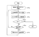
図3は、本技術の第1の実施形態における距離測定装置1Aによる測距処理方法を説明するためのフローチャートである。
すなわち、距離測定装置1Aは、測距処理を開始すると、まず、画素毎に露光のON/OFFを選択する(ステップST1a)。なお、このステップST1aにおいては、画素毎の動作周波数、つまり電荷蓄積部の切替周波数を選択するようにしてもよい。
続いて、距離測定装置1Aは、ON選択領域に合わせた露光を行い(ステップST1b)、露光された領域におけるデータを読み出し、読み出したデータに基づき、例えば1フレーム分の画素に対する測距データを算出する(ステップST1c)。
図3は、本技術の第1の実施形態における距離測定装置1Aによる測距処理方法を説明するためのフローチャートである。
すなわち、距離測定装置1Aは、測距処理を開始すると、まず、画素毎に露光のON/OFFを選択する(ステップST1a)。なお、このステップST1aにおいては、画素毎の動作周波数、つまり電荷蓄積部の切替周波数を選択するようにしてもよい。
続いて、距離測定装置1Aは、ON選択領域に合わせた露光を行い(ステップST1b)、露光された領域におけるデータを読み出し、読み出したデータに基づき、例えば1フレーム分の画素に対する測距データを算出する(ステップST1c)。
そして、距離測定装置1Aは、終了か否かの判定を行い(ステップST1d)、終了でない場合(No)、ROI領域判定部80により、算出された測距データからROIとなる物体OBJが存在し、ROIの位置が変更されたか否かの判定を行う(ステップST1e)。ここでの終了処理は、例えば外部から終了する旨の信号を受信した場合に、終了される。ここで、ROIの位置に変更が無ければ(No)、距離測定装置1Aは、上記ステップST1bの処理に移行する。一方、ROIとなる物体OBJの位置が変更された場合に(Yes)、距離測定装置1Aは、画素変調部90Aを制御して物体OBJに該当する画素に対し、露光のON/OFF領域を更新し(ステップST1f)、上記ステップST1aの処理に移行する。なお、ステップST1fにおいて、距離測定装置1Aは、画素変調部90Aを制御して物体OBJに該当する画素における動作周波数、つまり電荷蓄積部の切替周波数を高い周波数に変更するようにしてもよい。また、露光のON領域の変更、電荷蓄積部の切替周波数の変更のトリガについては、ROI領域判定部80による判定結果以外に、例えば外部カメラ画像を用いて画像認識であっても、外部から物体OBJがある旨の信号を受信するようにしてもよい。この場合、物体OBJに対応する画素エリアの切替周波数を変更する。
さらに、物体OBJがある旨の信号を用いて画素エリアの切替周波数を変更させなくても、予めエリアの切り分けとエリアごとの周波数を決めて、インプットさせておいてもよい。
また、上記ステップST1dの処理に戻って、距離測定装置1Aは、終了と判定した場合(Yes)、処理をそのまま終了する。
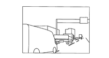
このようにして、距離測定装置1Aは、図4に示すように、先に測距がなされた隣接するラインの画素による物体OBJまでの距離に応じて、画素における電荷蓄積部の切替周波数を適宜変更することができる。とりわけ、測距の結果、物体OBJまでの距離が近い場合、より高い測距精度での測距が可能になるように高い切替周波数に変更される。これにより、例えば、車両前方のシーンにおいて、近くの障害物(例えば他の車両)については、より高い測距精度での測距により、衝突等の回避をより正確に行えるようになる。一方、測距の結果、近くに障害物(例えば他の車両)がない場合、より低い測距精度での測距を行うように低い切替周波数、もしくは切替周波数「0」に切り替えることで、画素の駆動電圧やプロセッサによる演算負荷を下げ、消費電力を抑えることができるようになる。
また、上記ステップST1dの処理に戻って、距離測定装置1Aは、終了と判定した場合(Yes)、処理をそのまま終了する。
このようにして、距離測定装置1Aは、図4に示すように、先に測距がなされた隣接するラインの画素による物体OBJまでの距離に応じて、画素における電荷蓄積部の切替周波数を適宜変更することができる。とりわけ、測距の結果、物体OBJまでの距離が近い場合、より高い測距精度での測距が可能になるように高い切替周波数に変更される。これにより、例えば、車両前方のシーンにおいて、近くの障害物(例えば他の車両)については、より高い測距精度での測距により、衝突等の回避をより正確に行えるようになる。一方、測距の結果、近くに障害物(例えば他の車両)がない場合、より低い測距精度での測距を行うように低い切替周波数、もしくは切替周波数「0」に切り替えることで、画素の駆動電圧やプロセッサによる演算負荷を下げ、消費電力を抑えることができるようになる。
<露光時の電力削減>
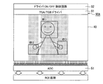
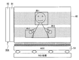
図5は、本技術の第1の実施形態において、ROI領域のみデータを出力する場合の一例を示すブロック図である。図5の例では、画素変調部90Aは、TGA/TGBドライバ91と、ドライバON/OFF制御回路92とを備える。TGA/TGBドライバ91は、画素41内の電荷蓄積部の切り替えを行うための転送信号TGA、TGBを出力するものである。ドライバON/OFF制御回路92は、システム制御部10による制御の下、ROI領域(図5では、例えば枠1、枠2、枠3を図示)のみ、画素41内の電荷蓄積部の切り替えを行うようにTGA/TGBドライバ91を制御する。
図5は、本技術の第1の実施形態において、ROI領域のみデータを出力する場合の一例を示すブロック図である。図5の例では、画素変調部90Aは、TGA/TGBドライバ91と、ドライバON/OFF制御回路92とを備える。TGA/TGBドライバ91は、画素41内の電荷蓄積部の切り替えを行うための転送信号TGA、TGBを出力するものである。ドライバON/OFF制御回路92は、システム制御部10による制御の下、ROI領域(図5では、例えば枠1、枠2、枠3を図示)のみ、画素41内の電荷蓄積部の切り替えを行うようにTGA/TGBドライバ91を制御する。
<画素の等価回路>
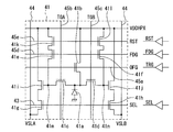
図6は、画素41の等価回路を示す。
画素41は、フォトダイオード41a、排出トランジスタ41b、転送トランジスタ41c,41d、変換効率調整トランジスタ41e,41f、選択トランジスタ41g,41h、増幅トランジスタ41i,41j、及びリセットトランジスタ41k,41lを含む。排出トランジスタ41b、転送トランジスタ41c,41d、変換効率調整トランジスタ41e,41f、選択トランジスタ41g,41h、増幅トランジスタ41i,41j、及びリセットトランジスタ41k,41lは、例えばMOSトランジスタで構成されている。
図6は、画素41の等価回路を示す。
画素41は、フォトダイオード41a、排出トランジスタ41b、転送トランジスタ41c,41d、変換効率調整トランジスタ41e,41f、選択トランジスタ41g,41h、増幅トランジスタ41i,41j、及びリセットトランジスタ41k,41lを含む。排出トランジスタ41b、転送トランジスタ41c,41d、変換効率調整トランジスタ41e,41f、選択トランジスタ41g,41h、増幅トランジスタ41i,41j、及びリセットトランジスタ41k,41lは、例えばMOSトランジスタで構成されている。
フォトダイオード41aは、入射光を光電変換する光電変換部を構成する。フォトダイオード41aのアノードは接地されている。フォトダイオード41aのカソードには、転送トランジスタ41c,41dのソース及び排出トランジスタ41bのソースが接続されている。
排出トランジスタ41bのドレインには電源電圧VDDHPXが印加される。排出トランジスタ41bのゲートには、排出制御配線45aを介して排出信号OFGが印加される。排出トランジスタ41bは、排出信号OFGに基づき、フォトダイオード41aの電荷を排出する。なお、排出トランジスタ41bが無い構成であってもよい。
排出トランジスタ41bのドレインには電源電圧VDDHPXが印加される。排出トランジスタ41bのゲートには、排出制御配線45aを介して排出信号OFGが印加される。排出トランジスタ41bは、排出信号OFGに基づき、フォトダイオード41aの電荷を排出する。なお、排出トランジスタ41bが無い構成であってもよい。
転送トランジスタ41c,41dのドレインは、浮遊拡散領域(フローティング・ディフュージョン)で構成される電荷蓄積部41m,41nにそれぞれ接続されている。転送トランジスタ41c,41dのゲートには、TGA/TGBドライバ91から出力される転送信号TGA,TGBが制御線45b,45cを介してそれぞれ印加される。転送トランジスタ41c,41dは、転送信号TGA,TGBに基づき、フォトダイオード41aからの電荷を電荷蓄積部41m,41nにそれぞれ転送する。
電荷蓄積部41m,41nは、フォトダイオード41aから転送トランジスタ41c,41dを介して転送された電荷を蓄積する。電荷蓄積部41m,41nに蓄積された電荷量に応じて、電荷蓄積部41m,41nの電位は変調される。
電荷蓄積部41m,41nには、変換効率調整トランジスタ41e,41fのソースがそれぞれ接続されている。変換効率調整トランジスタ41e,41fのドレインは、リセットトランジスタ41k,41lのソースにそれぞれ接続されている。変換効率調整トランジスタ41e,41fのゲートには、変換効率調整配線45dを介して共通の変換効率調整信号FDGが印加される。変換効率調整トランジスタ41e,41fは、変換効率調整信号FDGに応じて、電荷の変換効率を調整する。なお、変換効率調整トランジスタ41e,41fが無い構成であってもよい。その場合、電荷蓄積部41m,41nには、リセットトランジスタ41k,41lのソースがそれぞれ接続される。
電荷蓄積部41m,41nには、変換効率調整トランジスタ41e,41fのソースがそれぞれ接続されている。変換効率調整トランジスタ41e,41fのドレインは、リセットトランジスタ41k,41lのソースにそれぞれ接続されている。変換効率調整トランジスタ41e,41fのゲートには、変換効率調整配線45dを介して共通の変換効率調整信号FDGが印加される。変換効率調整トランジスタ41e,41fは、変換効率調整信号FDGに応じて、電荷の変換効率を調整する。なお、変換効率調整トランジスタ41e,41fが無い構成であってもよい。その場合、電荷蓄積部41m,41nには、リセットトランジスタ41k,41lのソースがそれぞれ接続される。
リセットトランジスタ41k,41lのドレインには、電源電位VDDHPXが印加される。リセットトランジスタ41k,41lのゲートには、共通のリセット制御配線45eを介してリセット信号RSTが印加される。リセットトランジスタ41k,41lは、リセット信号RSTに基づき、電荷蓄積部41m,41nに蓄積されていた電荷を初期化(リセット)する。なお、電荷蓄積部41m,41nに個別に接続されたリセットトランジスタ41k,41lを設ける代わりに、電荷蓄積部41m,41nに共通に接続された1つのリセットトランジスタを設けてもよい。
電荷蓄積部41m,41nには、増幅トランジスタ41i,41jのゲートが接続されている。増幅トランジスタ41i,41jのドレインには、選択トランジスタ41g,41hのソースが接続されている。増幅トランジスタ41i,41jは、電荷蓄積部41m,41nの電位を増幅する。
選択トランジスタ41g,41hのドレインは、垂直信号線44にそれぞれ接続されている。選択トランジスタ41g,41hのゲートには、画素駆動線43を介して選択信号SELが印加される。選択トランジスタ41g,41hは、選択信号SELに基づき、画素41を選択する。画素41が選択された場合、増幅トランジスタ41i,41jにより増幅された電位に応じた画素信号VSLA、VSLBが垂直信号線44を介して出力される。
選択トランジスタ41g,41hのドレインは、垂直信号線44にそれぞれ接続されている。選択トランジスタ41g,41hのゲートには、画素駆動線43を介して選択信号SELが印加される。選択トランジスタ41g,41hは、選択信号SELに基づき、画素41を選択する。画素41が選択された場合、増幅トランジスタ41i,41jにより増幅された電位に応じた画素信号VSLA、VSLBが垂直信号線44を介して出力される。
枠内の画素41の電荷の蓄積時間において、リセット信号RSTとしてL(ロー)レベルをリセットトランジスタ41k,41lのゲートに印加するため、リセットトランジスタ41k,41lは非導通状態となる。また、転送信号TGA,TGBとしてHレベル及びLレベルを逆位相で繰り返して、転送トランジスタ41c,41dのゲートに印加する。転送信号TGAは、例えば発光部20の発光パターンと同一位相とし、転送信号TGBは、発光部20の発光パターンと逆位相とする。転送トランジスタ41c,41dは、導通状態と非導通状態を逆位相で繰り返すことにより、電荷蓄積部41m,41nに電荷を振り分ける。
読み出し期間において、転送信号TGA,TGBとしてLレベルを転送トランジスタ41c,41dのゲートに印加するため、転送トランジスタ41c,41dは非導通状態となる。このとき、選択信号SELとしてHレベルを選択トランジスタ41g,41hのゲートに印加する。選択トランジスタ41g,41hは導通状態となり、電荷蓄積部41m,41nの電荷量が読み出され、電荷量に応じた画素信号が、図1に示した測距処理部50に出力される。
図5に戻り、ドライバON/OFF制御回路92は、垂直方向(V方向)で転送信号TGA,TGBの制御線45b,45cが共通の場合に、V方向にROI領域(図5では、枠1、枠2、枠3)がある画素41のみ転送信号TGA,TGBの切り替えを行うようにTGA/TGBドライバ91を制御する。従って、距離測定装置1A全体の消費電力を抑えることができる。
図5に戻り、ドライバON/OFF制御回路92は、垂直方向(V方向)で転送信号TGA,TGBの制御線45b,45cが共通の場合に、V方向にROI領域(図5では、枠1、枠2、枠3)がある画素41のみ転送信号TGA,TGBの切り替えを行うようにTGA/TGBドライバ91を制御する。従って、距離測定装置1A全体の消費電力を抑えることができる。
<露光時の電力削減の変形例>
図7は、本技術の第1の実施形態の第1の変形例における、ROI領域のみデータを出力する場合の一例を示すブロック図である。
図7の例では、水平方向(H方向)で転送信号TGA,TGBの制御線45b,45cが共通の場合を示す。この第1の変形例であっても、ドライバON/OFF制御回路92は、H方向で転送信号TGA,TGBの制御線45b,45cが共通の場合に、H方向にROI領域(図7では、枠1、枠2、枠3)がある画素41のみ転送信号TGA,TGBの切り替えを行うようにTGA/TGBドライバ91を制御する。従って、距離測定装置1A全体の消費電力を抑えることができる。
図7は、本技術の第1の実施形態の第1の変形例における、ROI領域のみデータを出力する場合の一例を示すブロック図である。
図7の例では、水平方向(H方向)で転送信号TGA,TGBの制御線45b,45cが共通の場合を示す。この第1の変形例であっても、ドライバON/OFF制御回路92は、H方向で転送信号TGA,TGBの制御線45b,45cが共通の場合に、H方向にROI領域(図7では、枠1、枠2、枠3)がある画素41のみ転送信号TGA,TGBの切り替えを行うようにTGA/TGBドライバ91を制御する。従って、距離測定装置1A全体の消費電力を抑えることができる。
<露光時の電力削減の他の変形例>
図8は、本技術の第1の実施形態の第2の変形例における、ROI領域のみデータを出力する場合の一例を示すブロック図である。
図8の例では、複数画素単位でV方向の制御線45b,45cを、V方向に複数の領域に分けて、細かい領域で転送信号TGA,TGBの切り替えをON/OFF可能にしてもよい。なお、H方向の制御線45b,45cを分けてもよい。
図8は、本技術の第1の実施形態の第2の変形例における、ROI領域のみデータを出力する場合の一例を示すブロック図である。
図8の例では、複数画素単位でV方向の制御線45b,45cを、V方向に複数の領域に分けて、細かい領域で転送信号TGA,TGBの切り替えをON/OFF可能にしてもよい。なお、H方向の制御線45b,45cを分けてもよい。
<第1の実施形態の作用効果>
以上のように上記第1の実施形態によれば、画素変調部90Aにおいて、撮像フレーム中の画素領域ごとに、電荷蓄積部41m,41nを切り替える切替周波数を異ならせることができる。これにより、高速で測距したい画素領域が撮像フレーム中の一部である場合に、読み出したい画素領域を枠1、枠2、枠3と複数指定可能にし、読み出したい領域のみ他の領域より高い切替周波数により電荷蓄積部41m,41nの切替制御を実行することで、電力を削減できる。
また、上記第1の実施形態によれば、データを出力するROI領域のみ、転送トランジスタ41c,41dそれぞれのゲートに供給する転送信号TGA,TGBの切り替えを行うことで、消費電力を抑えることができる。
さらに、上記第1の実施形態によれば、距離測定装置1A内に、ROI領域判定部80を設けているので、リアルタイムで撮像フレーム中の画素領域ごとに、電荷蓄積部41m,41nの切替制御を実行できる。
以上のように上記第1の実施形態によれば、画素変調部90Aにおいて、撮像フレーム中の画素領域ごとに、電荷蓄積部41m,41nを切り替える切替周波数を異ならせることができる。これにより、高速で測距したい画素領域が撮像フレーム中の一部である場合に、読み出したい画素領域を枠1、枠2、枠3と複数指定可能にし、読み出したい領域のみ他の領域より高い切替周波数により電荷蓄積部41m,41nの切替制御を実行することで、電力を削減できる。
また、上記第1の実施形態によれば、データを出力するROI領域のみ、転送トランジスタ41c,41dそれぞれのゲートに供給する転送信号TGA,TGBの切り替えを行うことで、消費電力を抑えることができる。
さらに、上記第1の実施形態によれば、距離測定装置1A内に、ROI領域判定部80を設けているので、リアルタイムで撮像フレーム中の画素領域ごとに、電荷蓄積部41m,41nの切替制御を実行できる。
<第2の実施形態>
次に、第2の実施形態について説明する。第2の実施形態は、第1の実施形態の変形であり、撮像フレーム全面のデータを読み出す場合について説明する。
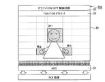
図9は、本技術の第2の実施形態における全面データを出力する場合の一例を示すブロック図である。図9の例では、画素変調部90Bは、TGA/TGBドライバ91と、発光タイミング切替回路93とを備える。発光タイミング切替回路93は、システム制御部10から出力されるROI領域情報に基づき、ROI領域(図9では、例えば枠1、枠2、枠3を図示)では、高速(例えば、100MHz)で画素41内の電荷蓄積部41m,41nの切り替えを行い、それ以外の領域では低い周波数(例えば、50MHz)で画素41内の電荷蓄積部41m,41nの切り替えを行うようにTGA/TGBドライバ91を制御する。
次に、第2の実施形態について説明する。第2の実施形態は、第1の実施形態の変形であり、撮像フレーム全面のデータを読み出す場合について説明する。
図9は、本技術の第2の実施形態における全面データを出力する場合の一例を示すブロック図である。図9の例では、画素変調部90Bは、TGA/TGBドライバ91と、発光タイミング切替回路93とを備える。発光タイミング切替回路93は、システム制御部10から出力されるROI領域情報に基づき、ROI領域(図9では、例えば枠1、枠2、枠3を図示)では、高速(例えば、100MHz)で画素41内の電荷蓄積部41m,41nの切り替えを行い、それ以外の領域では低い周波数(例えば、50MHz)で画素41内の電荷蓄積部41m,41nの切り替えを行うようにTGA/TGBドライバ91を制御する。
第2の実施形態では、発光タイミング調整部30は、複数の周波数分の発光タイミングを生成し、画素変調部90Bに出力する。画素変調部90Bは、システム制御部10から出力されるROI領域情報から、その発光タイミング(周波数)のパルスを使用するか選択する。
次に、図10のタイミングチャートを参照して、第2の実施形態に係る測距方法を、ROIの枠内及び枠外に着目して説明する。
発光部20は、所定の発光タイミング(例えば、100MHz)で照射のオン/オフを繰り返すように変調された照射光を発光する(図10(1))。物体OBJまでの距離に応じた遅延時間(ΔT)だけ遅れて、画素41内のフォトダイオード41aにおいて反射光が受光される(図10(2))。
次に、図10のタイミングチャートを参照して、第2の実施形態に係る測距方法を、ROIの枠内及び枠外に着目して説明する。
発光部20は、所定の発光タイミング(例えば、100MHz)で照射のオン/オフを繰り返すように変調された照射光を発光する(図10(1))。物体OBJまでの距離に応じた遅延時間(ΔT)だけ遅れて、画素41内のフォトダイオード41aにおいて反射光が受光される(図10(2))。
枠内の画素41の電荷の蓄積時間において、リセット信号RSTとしてL(ロー)レベルをリセットトランジスタ41k,41lのゲートに印加するため、リセットトランジスタ41k,41lは非導通状態となる。また、転送信号TGA,TGBとしてHレベル及びLレベルを逆位相で繰り返して、転送トランジスタ41c,41dのゲートに印加する。転送信号TGAは、例えば発光部20の発光パターンと同一位相とし(図10(3))、転送信号TGBは、発光部20の発光パターンと逆位相とする(図10(4))。転送トランジスタ41c,41dは、導通状態と非導通状態を100MHzの切替周波数で繰り返すことにより、電荷蓄積部41m,41nに電荷を振り分ける。
読み出し期間において、転送信号TGA,TGBとしてLレベルを転送トランジスタ41c,41dのゲートに印加するため、転送トランジスタ41c,41dは非導通状態となる。このとき、選択信号SELとしてHレベルを選択トランジスタ41g,41hのゲートに印加する。選択トランジスタ41g,41hは導通状態となり、電荷蓄積部41m,41nの電荷量が読み出され、電荷量に応じた画素信号S11(図10(3)、(4)ではドットで示す箇所)が、図1に示した測距処理部50に出力される。
枠外の画素41の電荷の蓄積時間において、リセット信号RSTとしてLレベルをリセットトランジスタ41k,41lのゲートに印加するため、リセットトランジスタ41k,41lは非導通状態となる。また、転送信号TGA,TGBとしてHレベル及びLレベルを逆位相で繰り返して、転送トランジスタ41c,41dのゲートに印加する。転送信号TGAは、例えば発光部20の発光パターンと同一位相とし(図10(5))、転送信号TGBは、発光部20の発光パターンと逆位相とする(図10(6))。転送トランジスタ41c,41dは、導通状態と非導通状態を例えば50MHzの切替周波数で繰り返すことにより、電荷蓄積部41m,41nに電荷を振り分ける。
読み出し期間において、転送信号TGA,TGBとしてLレベルを転送トランジスタ41c,41dのゲートに印加するため、転送トランジスタ41c,41dは非導通状態となる。このとき、選択信号SELとしてHレベルを選択トランジスタ41g,41hのゲートに印加する。選択トランジスタ41g,41hは導通状態となり、電荷蓄積部41m,41nの電荷量が読み出され、電荷量に応じた画素信号S12(図10(5)、(6)ではドットで示す箇所)が、図1に示した測距処理部50に出力される。
<第2の実施形態の作用効果>
以上のように上記第2の実施形態によれば、画素変調部90Bにおいて、撮像フレームの全面データを読み出す場合も、領域ごとに転送信号TGA,TGBを切り替える速度を可変できるようにしておくことで、精度が高い情報が欲しいROI領域(枠1、枠2、枠3)については、高速で転送信号TGA,TGBを切り替え、精度が低くてよい領域(枠外)については、転送信号TGA,TGBを切り替える速度を落とすことで、距離測定装置1A全体として電力を削減することができる。
以上のように上記第2の実施形態によれば、画素変調部90Bにおいて、撮像フレームの全面データを読み出す場合も、領域ごとに転送信号TGA,TGBを切り替える速度を可変できるようにしておくことで、精度が高い情報が欲しいROI領域(枠1、枠2、枠3)については、高速で転送信号TGA,TGBを切り替え、精度が低くてよい領域(枠外)については、転送信号TGA,TGBを切り替える速度を落とすことで、距離測定装置1A全体として電力を削減することができる。
<第3の実施形態>
次に、第3の実施形態について説明する。第3の実施形態では、第1の実施形態の変形であり、TGA/TGBドライバ91及びドライバON/OFF制御回路92の具体的構成について説明する。
図11は、本技術の第3の実施形態におけるTGA/TGBドライバ91の一例を示すブロック図である。
図11において、TGA/TGBドライバ91は、例えば枠2に該当する画素41(図11では、画素Aとする)に対し周波数1A(100MHz)の信号と周波数2A(50MHz)の信号とを切り替えるスイッチ911aと、スイッチ911aから出力される信号を転送信号TGAに増幅して転送トランジスタ41cに出力するドライバ912aと、画素Aに対し周波数1B(100MHz)の信号と周波数2B(50MHz)の信号とを切り替えるスイッチ911bと、スイッチ911bから出力される信号を転送信号TGBに増幅して転送トランジスタ41dに出力するドライバ912bとを備えている。
次に、第3の実施形態について説明する。第3の実施形態では、第1の実施形態の変形であり、TGA/TGBドライバ91及びドライバON/OFF制御回路92の具体的構成について説明する。
図11は、本技術の第3の実施形態におけるTGA/TGBドライバ91の一例を示すブロック図である。
図11において、TGA/TGBドライバ91は、例えば枠2に該当する画素41(図11では、画素Aとする)に対し周波数1A(100MHz)の信号と周波数2A(50MHz)の信号とを切り替えるスイッチ911aと、スイッチ911aから出力される信号を転送信号TGAに増幅して転送トランジスタ41cに出力するドライバ912aと、画素Aに対し周波数1B(100MHz)の信号と周波数2B(50MHz)の信号とを切り替えるスイッチ911bと、スイッチ911bから出力される信号を転送信号TGBに増幅して転送トランジスタ41dに出力するドライバ912bとを備えている。
また、TGA/TGBドライバ91は、例えば枠1に該当する画素41(図11では、画素Cとする)に対し周波数1A(100MHz)の信号と周波数2A(50MHz)の信号とを切り替えるスイッチ913aと、スイッチ913aから出力される信号を転送信号TGAに増幅して転送トランジスタ41cに出力するドライバ914aと、画素Cに対し周波数1B(100MHz)の信号と周波数2B(50MHz)の信号とを切り替えるスイッチ913bと、スイッチ913bから出力される信号を転送信号TGBに増幅して転送トランジスタ41dに出力するドライバ914bとを備えている。
さらに、TGA/TGBドライバ91は、例えば枠3に該当する画素41(図11では、画素Bとする)に対し周波数1A(100MHz)の信号と周波数2A(50MHz)の信号とを切り替えるスイッチ915aと、スイッチ915aから出力される信号を転送信号TGAに増幅して転送トランジスタ41cに出力するドライバ916aと、画素Cに対し周波数1B(100MHz)の信号と周波数2B(50MHz)の信号とを切り替えるスイッチ915bと、スイッチ915bから出力される信号を転送信号TGBに増幅して転送トランジスタ41dに出力するドライバ916bとを備えている。
通常、画素A~Cは、周波数1A、周波数1Bにより動作しているが、画素Bのみ高速で測距したい場合、ドライバON/OFF制御回路92は画素Aに対するスイッチ911aを周波数2A側に切り替え、スイッチ911bを周波数2B側に切り替える。そして、画素Cに対するスイッチ913aを周波数2A側に切り替え、スイッチ913bを周波数2B側に切り替える。
なお、ドライバON/OFF制御回路92は画素Bに対するスイッチ915aを周波数1A側に切り替えた状態のままにし、スイッチ915bを周波数1B側に切り替えた状態のままにする。
なお、ドライバON/OFF制御回路92は画素Bに対するスイッチ915aを周波数1A側に切り替えた状態のままにし、スイッチ915bを周波数1B側に切り替えた状態のままにする。
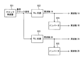
図12は、上記ドライバON/OFF制御回路92の一例を示すブロック図である。周波数1A,1B,2A,2Bの信号が互いに影響しないように、ドライバON/OFF制御回路92は、周波数1A,1B,2A,2Bの同期処理を行っている。
クロック発振器921から発生する基準クロック信号は、PLL(Phased Lock Loop)回路922,923に入力される。PLL回路922は、基準クロック信号をリファレンスとしてPLL処理することで、周波数1A(100MHz)の信号を生成する。この周波数1Aの信号は、インバータ924で逆位相の周波数1Bの信号に生成される。
PLL回路923は、基準クロック信号をリファレンスとしてPLL処理することで、周波数2A(50MHz)の信号を生成する。この周波数2Aの信号は、インバータ925で逆位相の周波数1Bの信号に生成される。
クロック発振器921から発生する基準クロック信号は、PLL(Phased Lock Loop)回路922,923に入力される。PLL回路922は、基準クロック信号をリファレンスとしてPLL処理することで、周波数1A(100MHz)の信号を生成する。この周波数1Aの信号は、インバータ924で逆位相の周波数1Bの信号に生成される。
PLL回路923は、基準クロック信号をリファレンスとしてPLL処理することで、周波数2A(50MHz)の信号を生成する。この周波数2Aの信号は、インバータ925で逆位相の周波数1Bの信号に生成される。
<第3の実施形態の作用効果>
以上のように上記第3の実施形態によれば、上記第1の実施形態と同様の作用効果が得られる。
以上のように上記第3の実施形態によれば、上記第1の実施形態と同様の作用効果が得られる。
<第4の実施形態>
次に、第4の実施形態について説明する。第4の実施形態では、第2の実施形態の変形であり、発光タイミング切替回路93の他の具体的構成について説明する。
図13は、上記発光タイミング切替回路93の一例を示すブロック図である。クロック発振器931から発生する基準クロック信号は、PLL回路932に入力される。PLL回路932は、基準クロック信号をリファレンスとしてPLL処理することで、周波数1A(100MHz)の信号を生成する。この周波数1Aの信号は、インバータ933で逆位相の周波数1Bの信号に生成される。
一方、周波数1Aの信号は、分周器934により例えば1/2に分周され、周波数2A(50MHz)の信号に生成される。分周器934は、インバータの機能を備え、周波数2A(50MHz)の信号から逆位相の周波数2Bの信号に生成し、出力する。
次に、第4の実施形態について説明する。第4の実施形態では、第2の実施形態の変形であり、発光タイミング切替回路93の他の具体的構成について説明する。
図13は、上記発光タイミング切替回路93の一例を示すブロック図である。クロック発振器931から発生する基準クロック信号は、PLL回路932に入力される。PLL回路932は、基準クロック信号をリファレンスとしてPLL処理することで、周波数1A(100MHz)の信号を生成する。この周波数1Aの信号は、インバータ933で逆位相の周波数1Bの信号に生成される。
一方、周波数1Aの信号は、分周器934により例えば1/2に分周され、周波数2A(50MHz)の信号に生成される。分周器934は、インバータの機能を備え、周波数2A(50MHz)の信号から逆位相の周波数2Bの信号に生成し、出力する。
<第4の実施形態の作用効果>
以上のように上記第4の実施形態によれば、上記第2の実施形態と同様の作用効果が得られる。さらに、上記第4の実施形態によれば、分周器934の分周比を変更するだけで、PLL回路を設ける場合に比べて、簡単な回路構成により、発光タイミング切替回路93を実現できる。このように、低周波数側に分周器934を用いることで、低周波数側を撮像し易くなる。
以上のように上記第4の実施形態によれば、上記第2の実施形態と同様の作用効果が得られる。さらに、上記第4の実施形態によれば、分周器934の分周比を変更するだけで、PLL回路を設ける場合に比べて、簡単な回路構成により、発光タイミング切替回路93を実現できる。このように、低周波数側に分周器934を用いることで、低周波数側を撮像し易くなる。
<第5の実施形態>
次に、第5の実施形態について説明する。第5の実施形態では、第4の実施形態の変形であり、発光タイミング切替回路93の他の具体的構成について説明する。
図14は、上記発光タイミング切替回路93の他の一例を示すブロック図である。図14において、上記図13と同一部分には同一符号を付して詳細な説明を省略する。
分周器935は、PLL回路932の出力を分周することで、周波数1A(100MHz)の信号を生成する。また、分周器935は、インバータの機能を備え、周波数1A(100MHz)の信号から逆位相の周波数1Bの信号に生成し、出力する。
次に、第5の実施形態について説明する。第5の実施形態では、第4の実施形態の変形であり、発光タイミング切替回路93の他の具体的構成について説明する。
図14は、上記発光タイミング切替回路93の他の一例を示すブロック図である。図14において、上記図13と同一部分には同一符号を付して詳細な説明を省略する。
分周器935は、PLL回路932の出力を分周することで、周波数1A(100MHz)の信号を生成する。また、分周器935は、インバータの機能を備え、周波数1A(100MHz)の信号から逆位相の周波数1Bの信号に生成し、出力する。
一方、周波数1Aの信号は、分周器936により例えば1/2に分周され、周波数2A(50MHz)の信号に生成される。分周器936は、インバータの機能を備え、周波数2A(50MHz)の信号から逆位相の周波数2Bの信号に生成し、出力する。
第5の実施形態では、例えば1GHzのPLL回路932のクロックから100MHzの切り替えパルスを生成する場合、分周器935の分周比を1:9~5:5~9:1に変更することで、パルスのハイ(High)/ロー(Low)期間を変更できる。
なお、周波数2A(50MHz)の信号については、PLL回路932の出力を分周あるいは分周器935で分周パルスをまとめて生成してもよい。
第5の実施形態では、例えば1GHzのPLL回路932のクロックから100MHzの切り替えパルスを生成する場合、分周器935の分周比を1:9~5:5~9:1に変更することで、パルスのハイ(High)/ロー(Low)期間を変更できる。
なお、周波数2A(50MHz)の信号については、PLL回路932の出力を分周あるいは分周器935で分周パルスをまとめて生成してもよい。
<第5の実施形態の作用効果>
以上のように上記第5の実施形態によれば、上記第2の実施形態と同様の作用効果が得られる。さらに、上記第5の実施形態によれば、分周器935の分周比を変更するだけで、高速な周波数1A,1Bの信号について、パルスのハイ(High)/ロー(Low)期間を変更できる。
以上のように上記第5の実施形態によれば、上記第2の実施形態と同様の作用効果が得られる。さらに、上記第5の実施形態によれば、分周器935の分周比を変更するだけで、高速な周波数1A,1Bの信号について、パルスのハイ(High)/ロー(Low)期間を変更できる。
<第6の実施形態>
次に、第6の実施形態について説明する。第6の実施形態では、上記測距処理部50から上記距離演算回路52を削除した測距処理部53とし、測距処理部53により算出された測距データを受信した外部のホストICを用いて、ROI領域を判定することを可能とする距離測定装置1Bが開示される。ここで、外部のホストICとは、上記第1の実施形態で説明したSoCとしての距離測定装置1Bの外部に設けられるという意味で用いられている。
次に、第6の実施形態について説明する。第6の実施形態では、上記測距処理部50から上記距離演算回路52を削除した測距処理部53とし、測距処理部53により算出された測距データを受信した外部のホストICを用いて、ROI領域を判定することを可能とする距離測定装置1Bが開示される。ここで、外部のホストICとは、上記第1の実施形態で説明したSoCとしての距離測定装置1Bの外部に設けられるという意味で用いられている。
図15は、本技術の第6の実施形態における距離測定装置1Bの構成の一例を示すブロック図である。同図に示すように、ホストIC2が、測距処理部53から通信インタフェース部60を介して受信した測距データに基づいて、上記距離演算回路52による処理を実行し、ROI領域を判定するように構成されている点で、上記第1の実施形態において図示したものと異なっている。なお、図15中、既に図示したコンポーネントと同一の機能ないし構成のコンポーネントについては、同一の符号を付し、適宜、その説明を省略する。
同図に示すように、本例では、図1に示した距離演算回路52及び図1に示したROI領域判定部80が、距離測定装置1A内に設けられる代わりに、ホストIC2に設けられている。図示していないが、ホストIC2は、対応する通信インタフェース部を含み構成される。ホストIC2の距離演算回路は、上記第1の実施形態と同様、測距処理部53から通信インタフェース部60を介して測距データを受信すると、物体OBJまでの距離を算出する。そして、ホストIC2のROI領域判定部は、該測距データに基づいて、ROI領域を判定する。ホストIC2のROI領域判定部は、該判定結果を、通信インタフェース部60を介して、システム制御部10に送信する。
一例として、ホストIC2は、1撮像フレーム分の測距データを保持し得るフレームバッファ(図示せず)を備え得る。ホストIC2のROI領域判定部は、フレームバッファを参照し、次の撮像フレームにおける読み出しラインごとにROI領域を判定する。
一例として、ホストIC2は、1撮像フレーム分の測距データを保持し得るフレームバッファ(図示せず)を備え得る。ホストIC2のROI領域判定部は、フレームバッファを参照し、次の撮像フレームにおける読み出しラインごとにROI領域を判定する。
<第6の実施形態の作用効果>
このようにして、上記第6の実施形態によっても、上記第1の実施形態と同様の作用効果ないしは利点を奏し得る。また、上記第3の実施形態によれば、距離測定装置1B内で距離演算回路による処理及びROI領域の判定処理を省略できる分、高度な処理が可能となる。特に、現在の撮像フレームの形成中に、該ROI領域の判定結果に基づいて、電荷蓄積部41m,41nの切替制御を実行できる。
このようにして、上記第6の実施形態によっても、上記第1の実施形態と同様の作用効果ないしは利点を奏し得る。また、上記第3の実施形態によれば、距離測定装置1B内で距離演算回路による処理及びROI領域の判定処理を省略できる分、高度な処理が可能となる。特に、現在の撮像フレームの形成中に、該ROI領域の判定結果に基づいて、電荷蓄積部41m,41nの切替制御を実行できる。
<その他の実施形態>
上記のように、本技術は第1から第6の実施形態によって記載したが、この開示の一部をなす論述及び図面は本技術を限定するものであると理解すべきではない。上記の実施形態が開示する技術内容の趣旨を理解すれば、当業者には様々な代替実施形態、実施例及び運用技術が本技術に含まれ得ることが明らかとなろう。また、第1から第6の実施形態及び第1から第6の実施形態の変形例がそれぞれ開示する構成を、矛盾の生じない範囲で適宜組み合わせることができる。例えば、複数の異なる実施形態がそれぞれ開示する構成を組み合わせてもよく、同一の実施形態の複数の異なる変形例がそれぞれ開示する構成を組み合わせてもよい。
上記のように、本技術は第1から第6の実施形態によって記載したが、この開示の一部をなす論述及び図面は本技術を限定するものであると理解すべきではない。上記の実施形態が開示する技術内容の趣旨を理解すれば、当業者には様々な代替実施形態、実施例及び運用技術が本技術に含まれ得ることが明らかとなろう。また、第1から第6の実施形態及び第1から第6の実施形態の変形例がそれぞれ開示する構成を、矛盾の生じない範囲で適宜組み合わせることができる。例えば、複数の異なる実施形態がそれぞれ開示する構成を組み合わせてもよく、同一の実施形態の複数の異なる変形例がそれぞれ開示する構成を組み合わせてもよい。
なお、本開示は以下のような構成も取ることができる。
(1)
行列状に配置され、対象領域からの反射光を受光し、前記反射光に応じて第1及び第2電荷蓄積部のいずれか一方に蓄積される電荷に基づく電気信号を出力する受光素子をそれぞれ有する複数の画素と、
前記複数の画素によって形成される撮像フレーム中の少なくとも一部の画素群による画素領域ごとに、互いに異なる切替周波数により前記第1及び第2電荷蓄積部の切替制御を実行する制御部と、
を備える撮像装置。
(2)
前記画素ごとに出力される前記電気信号を、アナログ信号からデジタル信号に変換するアナログ/デジタル変換部と、
前記アナログ/デジタル変換部の出力から、前記撮像フレーム中の関心領域までの距離を算出する距離算出部と、
をさらに備える前記(1)に記載の撮像装置。
(3)
前記受光素子は、前記第1及び第2電荷蓄積部に前記電荷をそれぞれ転送する第1及び第2転送トランジスタを備え、
前記制御部は、前記撮像フレーム中の関心領域に基づき、前記第1及び第2転送トランジスタそれぞれのゲートに供給する転送信号を切り替える、
前記(1)に記載の撮像装置。
(4)
前記制御部は、関心領域以外の領域において、前記第1及び第2転送トランジスタそれぞれのゲートに供給する転送信号を切り替える速度を、前記関心領域よりも遅くする、
前記(3)に記載の撮像装置。
(5)
測距算出部の出力から前記関心領域を判定する関心領域判定部を備え、
前記制御部は、前記関心領域判定部による前記関心領域の判定結果に基づいて、前記関心領域と関心領域以外の領域とで互いに異なる切替周波数により前記第1及び第2電荷蓄積部の切替制御を実行する、
前記(2)に記載の撮像装置。
(6)
前記制御部は、外部装置から提供される前記撮像フレーム中の関心領域の判定結果に基づいて、前記関心領域と関心領域以外の領域とで互いに異なる切替周波数により前記第1及び第2電荷蓄積部の切替制御を実行する、
前記(1)に記載の撮像装置。
(7)
行列状に配置され受光素子をそれぞれ有する複数の画素により対象領域からの反射光を受光し、前記反射光に応じて前記受光素子が備える第1及び第2電荷蓄積部に蓄積される電荷に基づく電気信号を出力することと、
前記複数の画素によって形成される撮像フレーム中の少なくとも一部の画素群による画素領域ごとに、互いに異なる切替周波数により前記第1及び第2電荷蓄積部の切替制御を実行することと、を含む、
撮像方法。
(1)
行列状に配置され、対象領域からの反射光を受光し、前記反射光に応じて第1及び第2電荷蓄積部のいずれか一方に蓄積される電荷に基づく電気信号を出力する受光素子をそれぞれ有する複数の画素と、
前記複数の画素によって形成される撮像フレーム中の少なくとも一部の画素群による画素領域ごとに、互いに異なる切替周波数により前記第1及び第2電荷蓄積部の切替制御を実行する制御部と、
を備える撮像装置。
(2)
前記画素ごとに出力される前記電気信号を、アナログ信号からデジタル信号に変換するアナログ/デジタル変換部と、
前記アナログ/デジタル変換部の出力から、前記撮像フレーム中の関心領域までの距離を算出する距離算出部と、
をさらに備える前記(1)に記載の撮像装置。
(3)
前記受光素子は、前記第1及び第2電荷蓄積部に前記電荷をそれぞれ転送する第1及び第2転送トランジスタを備え、
前記制御部は、前記撮像フレーム中の関心領域に基づき、前記第1及び第2転送トランジスタそれぞれのゲートに供給する転送信号を切り替える、
前記(1)に記載の撮像装置。
(4)
前記制御部は、関心領域以外の領域において、前記第1及び第2転送トランジスタそれぞれのゲートに供給する転送信号を切り替える速度を、前記関心領域よりも遅くする、
前記(3)に記載の撮像装置。
(5)
測距算出部の出力から前記関心領域を判定する関心領域判定部を備え、
前記制御部は、前記関心領域判定部による前記関心領域の判定結果に基づいて、前記関心領域と関心領域以外の領域とで互いに異なる切替周波数により前記第1及び第2電荷蓄積部の切替制御を実行する、
前記(2)に記載の撮像装置。
(6)
前記制御部は、外部装置から提供される前記撮像フレーム中の関心領域の判定結果に基づいて、前記関心領域と関心領域以外の領域とで互いに異なる切替周波数により前記第1及び第2電荷蓄積部の切替制御を実行する、
前記(1)に記載の撮像装置。
(7)
行列状に配置され受光素子をそれぞれ有する複数の画素により対象領域からの反射光を受光し、前記反射光に応じて前記受光素子が備える第1及び第2電荷蓄積部に蓄積される電荷に基づく電気信号を出力することと、
前記複数の画素によって形成される撮像フレーム中の少なくとも一部の画素群による画素領域ごとに、互いに異なる切替周波数により前記第1及び第2電荷蓄積部の切替制御を実行することと、を含む、
撮像方法。
1A,1B…距離測定装置、2…ホストIC、10…システム制御部、20…発光部、30…発光タイミング調整部、40…受光部、41…画素、41a…フォトダイオード、41b…排出トランジスタ、41c,41d…転送トランジスタ、41e,41f…変換効率調整トランジスタ、41g,41h…選択トランジスタ、41i,41j…増幅トランジスタ、41k,41l…リセットトランジスタ、41m,41n…電荷蓄積部、43…画素駆動線、44…垂直信号線、45a…排出制御配線、45b,45c…制御線、45d…変換効率調整配線、45e…リセット制御配線、50,53…測距処理部、51…AD変換部、52…距離演算回路、60…通信インタフェース部、70…画素駆動部、80…ROI領域判定部、90A,90B…画素変調部、91…TGA/TGBドライバ、92…ドライバON/OFF制御回路、93…発光タイミング切替回路、100…V(垂直)制御判定部、911a,911b,913a,913b,915a,915b…スイッチ、912a,912b,914a,914b,916a,916b…ドライバ、921,931…クロック発振器、922,923,932…PLL回路、924,925,933…インバータ、934,935,936…分周器
Claims (7)
- 行列状に配置され、対象領域からの反射光を受光し、前記反射光に応じて第1及び第2電荷蓄積部のいずれか一方に蓄積される電荷に基づく電気信号を出力する受光素子をそれぞれ有する複数の画素と、
前記複数の画素によって形成される撮像フレーム中の少なくとも一部の画素群による画素領域ごとに、互いに異なる切替周波数により前記第1及び第2電荷蓄積部の切替制御を実行する制御部と、
を備える撮像装置。 - 前記画素ごとに出力される前記電気信号を、アナログ信号からデジタル信号に変換するアナログ/デジタル変換部と、
前記アナログ/デジタル変換部の出力から、前記撮像フレーム中の関心領域までの距離を算出する距離算出部と、
をさらに備える請求項1に記載の撮像装置。 - 前記受光素子は、前記第1及び第2電荷蓄積部に前記電荷をそれぞれ転送する第1及び第2転送トランジスタを備え、
前記制御部は、前記撮像フレーム中の関心領域に基づき、前記第1及び第2転送トランジスタそれぞれのゲートに供給する転送信号を切り替える、
請求項1に記載の撮像装置。 - 前記制御部は、関心領域以外の領域において、前記第1及び第2転送トランジスタそれぞれのゲートに供給する転送信号を切り替える速度を、前記関心領域よりも遅くする、
請求項3に記載の撮像装置。 - 測距算出部の出力から前記関心領域を判定する関心領域判定部を備え、
前記制御部は、前記関心領域判定部による前記関心領域の判定結果に基づいて、前記関心領域と関心領域以外の領域とで互いに異なる切替周波数により前記第1及び第2電荷蓄積部の切替制御を実行する、
請求項2に記載の撮像装置。 - 前記制御部は、外部装置から提供される前記撮像フレーム中の関心領域の判定結果に基づいて、前記関心領域と関心領域以外の領域とで互いに異なる切替周波数により前記第1及び第2電荷蓄積部の切替制御を実行する、
請求項1に記載の撮像装置。 - 行列状に配置され受光素子をそれぞれ有する複数の画素により対象領域からの反射光を受光し、前記反射光に応じて前記受光素子が備える第1及び第2電荷蓄積部に蓄積される電荷に基づく電気信号を出力することと、
前記複数の画素によって形成される撮像フレーム中の少なくとも一部の画素群による画素領域ごとに、互いに異なる切替周波数により前記第1及び第2電荷蓄積部の切替制御を実行することと、を含む、
撮像方法。
Priority Applications (2)
| Application Number | Priority Date | Filing Date | Title |
|---|---|---|---|
| CN202180018639.0A CN115244918B (zh) | 2020-03-10 | 2021-01-18 | 成像装置和成像方法 |
| US17/908,494 US11895412B2 (en) | 2020-03-10 | 2021-01-18 | Imaging device and imaging method |
Applications Claiming Priority (2)
| Application Number | Priority Date | Filing Date | Title |
|---|---|---|---|
| JP2020-040719 | 2020-03-10 | ||
| JP2020040719 | 2020-03-10 |
Publications (1)
| Publication Number | Publication Date |
|---|---|
| WO2021181882A1 true WO2021181882A1 (ja) | 2021-09-16 |
Family
ID=77671705
Family Applications (1)
| Application Number | Title | Priority Date | Filing Date |
|---|---|---|---|
| PCT/JP2021/001497 Ceased WO2021181882A1 (ja) | 2020-03-10 | 2021-01-18 | 撮像装置及び撮像方法 |
Country Status (3)
| Country | Link |
|---|---|
| US (1) | US11895412B2 (ja) |
| CN (1) | CN115244918B (ja) |
| WO (1) | WO2021181882A1 (ja) |
Families Citing this family (2)
| Publication number | Priority date | Publication date | Assignee | Title |
|---|---|---|---|---|
| CN116868086A (zh) * | 2021-02-18 | 2023-10-10 | 索尼半导体解决方案公司 | 信号处理装置、信号处理方法和程序 |
| JP2026022856A (ja) * | 2024-07-31 | 2026-02-13 | Toppanホールディングス株式会社 | 距離画像撮像素子、及び距離画像撮像装置 |
Citations (3)
| Publication number | Priority date | Publication date | Assignee | Title |
|---|---|---|---|---|
| WO2017022220A1 (ja) * | 2015-08-04 | 2017-02-09 | パナソニックIpマネジメント株式会社 | 固体撮像装置 |
| JP2020013586A (ja) * | 2019-08-13 | 2020-01-23 | 株式会社ニコン | 撮像装置 |
| JP2020025265A (ja) * | 2018-07-31 | 2020-02-13 | ソニーセミコンダクタソリューションズ株式会社 | 固体撮像装置及び撮像装置 |
Family Cites Families (15)
| Publication number | Priority date | Publication date | Assignee | Title |
|---|---|---|---|---|
| KR20010090448A (ko) * | 2000-03-17 | 2001-10-18 | 시마무라 테루오 | 촬상장치 및 그 제조방법 및 그 촬상장치를 사용하는노광장치, 측정장치, 위치맞춤장치 및 수차측정장치 |
| JP2009008537A (ja) | 2007-06-28 | 2009-01-15 | Fujifilm Corp | 距離画像装置及び撮像装置 |
| US8686367B2 (en) * | 2012-03-01 | 2014-04-01 | Omnivision Technologies, Inc. | Circuit configuration and method for time of flight sensor |
| JP2013192058A (ja) * | 2012-03-14 | 2013-09-26 | Nikon Corp | 撮像装置 |
| KR20150061684A (ko) * | 2013-11-27 | 2015-06-05 | 삼성전자주식회사 | 엑스선 영상 장치 및 그 제어 방법 |
| CN103795410B (zh) * | 2014-01-24 | 2017-03-01 | 南京熊猫电子股份有限公司 | 一种基于双锁相环的宽带捷变频频率源 |
| JP6942966B2 (ja) * | 2016-03-16 | 2021-09-29 | 株式会社リコー | 物体検出装置及び移動体装置 |
| JP2018152696A (ja) * | 2017-03-13 | 2018-09-27 | ソニーセミコンダクタソリューションズ株式会社 | 固体撮像装置、その駆動方法および電子機器 |
| IL269008B2 (en) * | 2017-03-21 | 2023-10-01 | Magic Leap Inc | Depth sensing techniques for virtual, augmented and mixed reality systems |
| WO2019183912A1 (zh) * | 2018-03-30 | 2019-10-03 | 深圳市汇顶科技股份有限公司 | 模数转换电路、图像传感器和模数转换方法 |
| JP7161317B2 (ja) * | 2018-06-14 | 2022-10-26 | キヤノン株式会社 | 撮像装置、撮像システム及び移動体 |
| US11294039B2 (en) * | 2018-07-24 | 2022-04-05 | Samsung Electronics Co., Ltd. | Time-resolving image sensor for range measurement and 2D greyscale imaging |
| CN109792498B (zh) * | 2018-12-20 | 2021-02-23 | 深圳市汇顶科技股份有限公司 | 模数转换电路、图像传感器和模数转换方法 |
| US10878589B2 (en) * | 2019-05-02 | 2020-12-29 | Samsung Electronics Co., Ltd. | Time-of-flight depth measurement using modulation frequency adjustment |
| CN110221274B (zh) * | 2019-05-09 | 2021-04-30 | 奥比中光科技集团股份有限公司 | 时间飞行深度相机及多频调制解调的距离测量方法 |
-
2021
- 2021-01-18 US US17/908,494 patent/US11895412B2/en active Active
- 2021-01-18 CN CN202180018639.0A patent/CN115244918B/zh active Active
- 2021-01-18 WO PCT/JP2021/001497 patent/WO2021181882A1/ja not_active Ceased
Patent Citations (3)
| Publication number | Priority date | Publication date | Assignee | Title |
|---|---|---|---|---|
| WO2017022220A1 (ja) * | 2015-08-04 | 2017-02-09 | パナソニックIpマネジメント株式会社 | 固体撮像装置 |
| JP2020025265A (ja) * | 2018-07-31 | 2020-02-13 | ソニーセミコンダクタソリューションズ株式会社 | 固体撮像装置及び撮像装置 |
| JP2020013586A (ja) * | 2019-08-13 | 2020-01-23 | 株式会社ニコン | 撮像装置 |
Also Published As
| Publication number | Publication date |
|---|---|
| CN115244918A (zh) | 2022-10-25 |
| US20230095241A1 (en) | 2023-03-30 |
| CN115244918B (zh) | 2025-10-21 |
| US11895412B2 (en) | 2024-02-06 |
Similar Documents
| Publication | Publication Date | Title |
|---|---|---|
| JP7463671B2 (ja) | 距離画像撮像装置、及び距離画像撮像方法 | |
| CN107852470B (zh) | 固体摄像装置的驱动方法 | |
| US10666875B2 (en) | Solid-state imaging device | |
| WO2020145035A1 (ja) | 距離測定装置及び距離測定方法 | |
| US20200213540A1 (en) | Solid-state imaging device and imaging apparatus including same | |
| CN107852472B (zh) | 成像装置、成像方法和存储介质 | |
| US20220003876A1 (en) | Distance image obtaining method and distance detection device | |
| US11812171B2 (en) | Electronic device, method and computer program | |
| WO2021181882A1 (ja) | 撮像装置及び撮像方法 | |
| JP7356440B2 (ja) | 測距撮像装置、及び固体撮像素子 | |
| WO2021181868A1 (ja) | 測距センサ及び距離測定方法 | |
| JP7108471B2 (ja) | 固体撮像素子、撮像装置及び撮像方法 | |
| US11194025B2 (en) | Solid-state imaging device and imaging apparatus including same | |
| WO2021166523A1 (ja) | 距離測定装置及び距離測定方法 | |
| US20250123374A1 (en) | Measurement device | |
| WO2024085069A1 (ja) | 測距装置および測距方法 | |
| EP4703764A1 (en) | Image pickup apparatus, image pickup method, and computer program | |
| JP7199016B2 (ja) | 固体撮像装置 | |
| US20250044428A1 (en) | Distance measuring device and electronic device | |
| US20230115893A1 (en) | Distance measuring device and distance measuring method | |
| JP5146959B2 (ja) | 視差センサおよび視差画像の生成方法 | |
| WO2025127061A1 (ja) | 撮像装置および駆動方法 | |
| CN120201275A (zh) | 距离图像摄像装置以及距离图像摄像方法 | |
| JP2026049198A (ja) | 測距装置、測距方法、及びコンピュータプログラム | |
| JP2023028992A (ja) | 撮像装置およびその制御方法 |
Legal Events
| Date | Code | Title | Description |
|---|---|---|---|
| 121 | Ep: the epo has been informed by wipo that ep was designated in this application |
Ref document number: 21767732 Country of ref document: EP Kind code of ref document: A1 |
|
| NENP | Non-entry into the national phase |
Ref country code: DE |
|
| 122 | Ep: pct application non-entry in european phase |
Ref document number: 21767732 Country of ref document: EP Kind code of ref document: A1 |
|
| NENP | Non-entry into the national phase |
Ref country code: JP |
|
| WWG | Wipo information: grant in national office |
Ref document number: 202180018639.0 Country of ref document: CN |