WO2021181857A1 - 遅延補正回路および駆動回路 - Google Patents
遅延補正回路および駆動回路 Download PDFInfo
- Publication number
- WO2021181857A1 WO2021181857A1 PCT/JP2021/000834 JP2021000834W WO2021181857A1 WO 2021181857 A1 WO2021181857 A1 WO 2021181857A1 JP 2021000834 W JP2021000834 W JP 2021000834W WO 2021181857 A1 WO2021181857 A1 WO 2021181857A1
- Authority
- WO
- WIPO (PCT)
- Prior art keywords
- delay
- signal
- circuit
- unit
- delay circuit
- Prior art date
- Legal status (The legal status is an assumption and is not a legal conclusion. Google has not performed a legal analysis and makes no representation as to the accuracy of the status listed.)
- Ceased
Links
Images






Classifications
-
- G—PHYSICS
- G01—MEASURING; TESTING
- G01S—RADIO DIRECTION-FINDING; RADIO NAVIGATION; DETERMINING DISTANCE OR VELOCITY BY USE OF RADIO WAVES; LOCATING OR PRESENCE-DETECTING BY USE OF THE REFLECTION OR RERADIATION OF RADIO WAVES; ANALOGOUS ARRANGEMENTS USING OTHER WAVES
- G01S7/00—Details of systems according to groups G01S13/00, G01S15/00, G01S17/00
- G01S7/48—Details of systems according to groups G01S13/00, G01S15/00, G01S17/00 of systems according to group G01S17/00
- G01S7/483—Details of pulse systems
- G01S7/484—Transmitters
-
- H—ELECTRICITY
- H03—ELECTRONIC CIRCUITRY
- H03K—PULSE TECHNIQUE
- H03K5/00—Manipulating of pulses not covered by one of the other main groups of this subclass
-
- H—ELECTRICITY
- H03—ELECTRONIC CIRCUITRY
- H03K—PULSE TECHNIQUE
- H03K5/00—Manipulating of pulses not covered by one of the other main groups of this subclass
- H03K5/22—Circuits having more than one input and one output for comparing pulses or pulse trains with each other according to input signal characteristics, e.g. slope, integral
- H03K5/26—Circuits having more than one input and one output for comparing pulses or pulse trains with each other according to input signal characteristics, e.g. slope, integral the characteristic being duration, interval, position, frequency, or sequence
Definitions
- the present disclosure relates to a delay correction circuit and a drive circuit. More specifically, the present invention relates to a delay correction circuit that corrects the delay time of the delay circuit and a drive circuit that uses the delay correction circuit.
- a device that drives a light source such as a laser diode at a predetermined timing such as a distance measuring device that measures the distance to an object
- the distance to the object is measured by measuring the time for the light to reciprocate between the object and the object.
- light is output by driving the light source of the distance measuring device.
- This light is reflected by the object and becomes reflected light.
- This reflected light is detected by the optical sensor of the distance measuring device.
- the time from the output of this light to the detection of the reflected light is timed to calculate the distance.
- it is necessary to adjust the timing of driving the light source. This is to synchronize the light output with the reflected light detection operation.
- a delay circuit that delays the drive signal of the light source for a predetermined period of time is used to adjust the timing of driving the light source.
- the delay time can be managed by correcting the delay time.
- a distance measuring system including a circuit for setting a delay time of each delay element of a delay circuit configured by sequentially connecting a plurality of delay elements is used (see, for example, Patent Document 1).
- the drive timing is corrected by the first and second delay time control circuits that control the delay time of the drive signal.
- the delay time of the first and second delay time control circuits is managed by the delay synchronization loop circuit to a predetermined delay time.
- the delay time is corrected by the reference clock signal. This correction is performed by aligning the delay time of the delay synchronization loop circuit with the period of the reference clock signal by DLL (Delay Locked Loop).
- the above-mentioned conventional technology has a problem that the circuit size increases.
- the PLL is provided with a phase comparator that detects the phase difference between the reference clock signal and the reference clock signal that has passed through the delay synchronization loop circuit, and a low-pass filter that passes a low-frequency signal among the output signals of the phase comparator.
- This low-pass filter is composed of a passive element such as a capacitor and has a relatively large occupied area. Therefore, the delay correction circuit of the above-mentioned conventional technique has a problem that the circuit size increases.
- the present disclosure has been made in view of the above-mentioned problems, and an object of the present disclosure is to reduce the size of the delay correction circuit.
- the present disclosure has been made to solve the above-mentioned problems, and the first aspect thereof is a reference for generating a reference delay time which is a reference for the delay time of the signal of the signal delay circuit for delaying the signal.
- a phase comparator that compares the phases of the delay circuit, the signal delayed by the signal delay circuit, and the signal delayed by the reference delay circuit, and a delay of the signal delay circuit based on the comparison result of the phases.
- This is a delay correction circuit including a delay adjusting unit for adjusting the time and a reference delay circuit power supply unit for supplying power to the reference delay circuit.
- the reference delay circuit power supply unit may include a temperature correction power supply in which the output voltage changes based on a predetermined temperature coefficient.
- the reference delay circuit power supply unit may further include a temperature coefficient selection unit that selects the predetermined temperature coefficient.
- the reference delay circuit power supply unit may further include a temperature coefficient holding unit that holds the selection result in the temperature coefficient selection unit.
- the signal delay circuit may include a plurality of delay circuits having different delay times, and the delay adjusting unit may adjust the delay times of the plurality of delay circuits.
- an adjustment result holding unit for holding the delay adjustment result in the delay adjusting unit may be further provided.
- a reference delay adjusting unit for adjusting the reference delay time may be further provided.
- a reference delay adjustment result holding unit for holding the adjustment result of the reference delay time in the reference delay adjusting unit may be further provided.
- the reference delay adjusting unit may adjust the reference delay time to the middle delay time of the signal delay circuit.
- a second aspect of the present disclosure is a signal delay circuit that delays the drive signal, a reference delay circuit that generates a reference delay time that serves as a reference for the delay time of the drive signal, and the signal delay circuit.
- a phase comparator that compares the phase of the drive signal and the drive signal delayed by the reference delay circuit, a delay adjusting unit that adjusts the delay time of the signal delay circuit based on the comparison result of the phase, and the above.
- It is a drive circuit including a reference delay circuit power supply unit that supplies power to the reference delay circuit.
- the delay time of the signal delay circuit is adjusted by the reference delay circuit to which the power is supplied by the reference delay circuit power supply unit. It is expected that the power supply to the signal delay circuit will be reduced by the reference delay circuit power supply unit.
- FIG. 1 is a diagram showing a configuration example of a light source device according to the first embodiment of the present disclosure.
- the figure is a diagram showing a configuration example of the light source device 4.
- the light source device 4 includes a light source 41 and a drive circuit 42.
- the light source 41 emits light.
- the light source 41 can be configured by, for example, a laser diode.
- the drive circuit 42 is a circuit that drives the light source 41.
- the drive circuit 42 drives the light source 41 by supplying a light emitting current to the light source 41.
- the light emitting current is a current flowing through the light source 41 in order to cause the light source 41 to emit light.
- the drive circuit 42 drives the light source 41 based on a drive signal supplied from an external circuit.
- the drive signal is supplied via a differential transmission line composed of two lines. In the differential transmission line, drive signals having opposite phases are transmitted by two signal lines.
- LVDS Low Voltage Differential Signaling
- the drive circuit 42 includes a reception unit 600, a first signal delay circuit 200, a second signal delay circuit 300, a light emission drive signal generation unit 400, a drive unit 500, and a delay correction circuit 100.
- the receiving unit 600 receives the drive signal.
- the receiving unit 600 receives a drive signal that has been converted into a differential signal and transmitted.
- the reception unit 600 converts the received drive signal into a single-ended drive signal and outputs it to the first signal delay circuit 200 and the light emission drive signal generation unit 400. Further, the receiving unit 600 receives the calibration signal described later and outputs it to the first signal delay circuit 200 or the like.
- the first signal delay circuit 200 is a circuit that delays the drive signal output from the receiving unit 600 by a predetermined delay time.
- the first signal delay circuit 200 outputs the delayed drive signal to the second signal delay circuit 300.
- the delay time of the first signal delay circuit 200 is adjusted by the adjustment signal output from the delay correction circuit 100 described later.
- the delay time of the first signal delay circuit 200 is longer than the delay time of the second signal delay circuit 300 described below. Therefore, the resolution of the delay time at the time of adjustment becomes small.
- the adjustment of the delay time in the first signal delay circuit 200 corresponds to the rough adjustment. Details of the configuration of the first signal delay circuit 200 will be described later. Twice
- the second signal delay circuit 300 is a circuit that delays the drive signal output from the first signal delay circuit 200 by a predetermined delay time.
- the second signal delay circuit 300 outputs the delayed drive signal to the light emission drive signal generation unit 400.
- the delay time of the second signal delay circuit 300 is adjusted by the adjustment signal output from the delay correction circuit 100, which will be described later.
- the delay time of the second signal delay circuit 300 is shorter than the delay time of the first signal delay circuit 200, and the resolution is high.
- the adjustment of the delay time in the second signal delay circuit 300 corresponds to fine adjustment.
- the second signal delay circuit 300 outputs two drive signals having different delay times (delay drive signal 1 and delay drive signal 2 described later). Details of the configuration of the second signal delay circuit 300 will be described later.
- the light emission drive signal generation unit 400 generates a light emission drive signal from the drive signal or the like output from the reception unit 600 and the second signal delay circuit 300.
- the light emission drive signal is a drive signal of an element of the drive unit 500, which will be described later.
- the drive signal generated by the light emission drive signal generation unit 400 is output to the drive unit 500 and the delay correction circuit 100. The details of the configuration of the light emission drive signal generation unit 400 will be described later.
- the drive unit 500 supplies a drive current to the light source 41.
- the drive unit 500 supplies a drive current based on the light emission drive signal generated by the light emission drive signal generation unit 400. The details of the configuration of the drive unit 500 will be described later.
- the delay correction circuit 100 corrects the delay time of the first signal delay circuit 200 and the second signal delay circuit 300.
- the delay correction circuit 100 includes a reference delay circuit (reference delay circuit 110 described later) that generates a reference delay time that serves as a reference for the delay time, and delays of the first signal delay circuit 200 and the second signal delay circuit 300. The delay times of the first signal delay circuit 200 and the second signal delay circuit 300 are adjusted by comparing the time with the delay time of the reference delay circuit 110.
- the delay correction circuit 100 generates a calibration signal for adjusting the delay time, and inputs the calibration signal to the first signal delay circuit 200 via the receiving unit 600. After that, the light emission drive signal generated by the light emission drive signal generation unit 400 based on the drive signal delayed by the first signal delay circuit 200 and the second signal delay circuit 300 is input to the delay correction circuit 100.
- the delay correction circuit 100 inputs the calibration signal to its own reference delay circuit 110 to generate a calibration signal delayed by the reference delay time. Then, the delay correction circuit 100 compares the input light emission drive signal with the delayed calibration signal, adjusts the delay times of the first signal delay circuit 200 and the second signal delay circuit 300, and adjusts the delay time of the light emission drive signal. Is synchronized with the delayed calibration signal. Thereby, the delay time of the first signal delay circuit 200 and the second signal delay circuit 300 can be adjusted to the reference delay time.
- the process of adjusting the delay time of the first signal delay circuit 200 and the second signal delay circuit 300 is referred to as an adjustment process.
- the delay times of the first signal delay circuit 200 and the second signal delay circuit 300 are adjusted by the adjustment signals output individually. Details of the configuration of the delay correction circuit 100 will be described later.
- the drive signal is an example of the signal described in the claims.
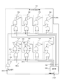
- FIG. 2 is a diagram showing a configuration example of the first signal delay circuit according to the embodiment of the present disclosure.
- the figure is a diagram showing a configuration example of the first signal delay circuit 200.
- the first signal delay circuit 200 in the figure includes an inverting gate 201, a delay unit 210, a delay unit 220, a delay unit 230, a delay unit 240, a delay unit 250, a delay unit 260, a delay unit 270, and a delay unit 280.
- a selection unit 290 is provided.
- the inversion gate 201 is a gate that inverts the drive signal output from the receiving unit 600.
- the drive signal output from the receiving unit 600 is hereinafter referred to as "drive signal'".
- the output of the reversing gate 201 is commonly input to the delay unit 210, the delay unit 220, the delay unit 230, the delay unit 240, the delay unit 250, the delay unit 260, the delay unit 270, and the delay unit 280.
- the delay unit 210, the delay unit 220, the delay unit 230, the delay unit 240, the delay unit 250, the delay unit 260, the delay unit 270, and the delay unit 280 are circuits that delay the drive signal'. These delay units 210 and the like are configured by the same circuit and are connected in series. That is, the output of the delay unit 210 is connected to the input of the delay unit 220, and the output of the delay unit 220 is connected to the input of the delay unit 230. They are connected in the following order, and the output of the delay unit 280 becomes the output of the first signal delay circuit 200 and is connected to the second signal delay circuit 300.
- the input of the delay unit 210 is grounded and the value "0" is input.
- the circuit configuration will be described by taking the delay unit 210 as an example.
- the delay unit 210 includes two input NOR gates 211 and 212 and an inversion gate 213.
- a signal line 209 and a signal line 291a are connected to the input of the NOR gate 211.
- the signal line 209 is a signal line that transmits the output signal of the above-mentioned inversion gate 201.
- the drive signal'inverted from the signal line 209 is input to the NOR gate 211.
- the signal line 291a is a signal line for transmitting a selection signal from the selection unit 290, which will be described later.
- the output of the NOR gate 211 and the signal line 219 are connected to the input of the NOR gate 212.
- the signal line 219 corresponds to the input node of the delay unit 210, and is a node to which the output signal of the delay unit in the previous stage is input. As described above, the signal line 219 is grounded and the value "0" is input.
- the output of the NOR gate 212 is connected to the input of the inverting gate 213, and the output of the inverting gate 213 is connected to the signal line 229.
- the signal line 229 corresponds to the output node of the delay unit 210 and also corresponds to the input node of the delay unit of the next stage.
- the delay time per stage by the delay unit 210 or the like is 100 to 150 ps, which is the sum of the delay times of the NOR gate and the inversion gate.
- the selection unit 290 selects one of the delay units 210 and the like based on the adjustment signal from the delay correction circuit 100.
- the selection unit 290 selects the delay unit 210 and the like by outputting a selection signal to any one of the plurality of signal lines 291.
- the selection unit 290 adjusts the delay time of the first signal delay circuit 200 by selecting the delay unit 210 or the like.
- the selection unit 290 outputs the value "0" to the signal line 291 connected to the selected delay unit 210 or the like, and outputs the value "1" to the other delay unit 210 or the like to select the delay unit 210 or the like. I do.
- the operation of the first signal delay circuit 200 will be described by taking the case where the delay unit 210 is selected as an example.
- the selection unit 290 outputs the value "0" to the signal line 291a.
- the inverted drive signal'input via the signal line 209 is further inverted and output to the output of the NOR gate 211. Since the value "0" is input to the other inputs of the two-input NOR gate 212 via the signal line 219, the inverted drive signal'is output to the output of the NOR gate 212.
- This inverted drive signal'is again by the inversion gate 213, output to the signal line 229, and input to the delay unit 220.
- the output of the NOR gate 221 of the delay unit 220 becomes the value "0", and the drive signal input to the delay unit 220.
- the drive signal' is transmitted in order from the delay unit 230 to the delay unit 280. In this case, a delay time of 8 steps can be obtained.
- the value "0" is output to the signal line 291b.
- the unselected delay unit 210 outputs the signal of the signal line 219 to the signal line 229. Since the value "0" is input to the signal line 219, the delay unit 210 outputs the value "0" to the signal line 229.
- a value "0” is input to the input node of the delay unit 220, and is input to the NOR gate 222. Therefore, the drive signal'is transmitted from the delay unit 220 to the delay unit 280.
- the delay time is 7 steps. In this way, the delay time of the first signal delay circuit 200 can be adjusted according to the position of the delay unit 210 or the like selected by the selection unit 290.
- the delay correction circuit 100 For the adjustment signal from the delay correction circuit 100, for example, a 3-bit digital signal can be used. With this 3-bit adjustment signal, the delay correction circuit 100 sets the number of delay stages in the first signal delay circuit 200. The delay unit 210 or the like corresponding to the number of delay stages is selected by the selection unit 290. Thereby, the delay time of the first signal delay circuit 200 can be adjusted by the delay correction circuit 100.
- the selection unit 290 can select the delay unit 210 when the adjustment signal of the value "0" is input, and select the delay unit 280 when the adjustment signal of the value "7" is input.
- the medium delay time corresponds to a delay time that is approximately half of the maximum delay time that can be set in the first signal delay circuit 200 or the like.
- FIG. 3 is a diagram showing a configuration example of a second signal delay circuit according to the embodiment of the present disclosure.
- the figure is a diagram showing a configuration example of the second signal delay circuit 300.
- a in the figure represents a circuit diagram of the second signal delay circuit 300
- B in the figure is a circuit diagram showing a configuration example of a delay portion used in the second signal delay circuit 300.
- the second signal delay circuit 300 represented by A in the figure is selected from the delay unit 310, the delay unit 320, the delay unit 330, the delay unit 340, the delay unit 350, the delay unit 360, the delay unit 370, and the delay unit 380.
- a unit 390 is provided.
- the delay unit 310, the delay unit 320, the delay unit 330, the delay unit 340, the delay unit 350, the delay unit 360, the delay unit 370, and the delay unit 380 delay the drive signal'output from the first signal delay circuit 200. It is a circuit. Similar to the delay section 210 and the like described above, these delay sections 310 and the like are configured by the same circuit and are connected in cascade. The delay unit 310 and the like are configured by an inversion gate whose delay time can be changed. A signal line 391 for transmitting a selection signal from the selection unit 390 is wired to the delay unit 310 and the like. The delay time of the delay unit 310 and the like is changed by this selection signal.
- the delay unit 310 or the like to which the selection signal of the value "1" is input has a long delay time
- the delay unit 310 or the like to which the selection signal of the value "0" is input may change to a short delay time. can.
- the output of the delay unit 380 is the output of the second signal delay circuit 300, and the drive signal'output from the first signal delay circuit 200'is a signal delayed by all the delay units 310 and the like. Is output. Further, the second signal delay circuit 300 further outputs a delay drive signal 1 which is a signal delayed by a part of the delay unit 310 or the like.
- the delay drive signal 1 can be obtained from the output of the delay portion in the middle stage of the delay portions 310 and the like which are connected in cascade. A in the figure represents an example in which the delay drive signal 1 is generated from the output of the delay unit 340.
- the selection unit 390 selects the delay unit 310 and the like based on the adjustment signal from the delay correction circuit 100.
- the selection unit 390 selects the delay unit 310 and the like by outputting selection signals to a plurality of signal lines 391.
- the selection unit 390 adjusts the delay time of the second signal delay circuit 300 by selecting the delay unit 310 and the like.
- the selection unit 390 can output the value "0" as a selection signal. In this case, the selection unit 390 outputs the value "1" to the non-selection delay unit 310 or the like.
- the delay unit 310 or the like in which the value "0" is input as the selection signal changes to a short delay time. Therefore, the delay time of the second signal delay circuit 300 can be adjusted according to the number of the delay units 310 and the like to be selected.
- the delay correction circuit 100 For the adjustment signal from the delay correction circuit 100, for example, a 3-bit digital signal can be used. With this 3-bit adjustment signal, the delay correction circuit 100 sets the number of delay stages in the second signal delay circuit 300, and the delay unit 310 or the like corresponding to the number of delay stages is selected by the selection unit 390. Thereby, the delay time of the second signal delay circuit 300 can be adjusted by the delay correction circuit 100. For example, when the adjustment signal of the value "0" is input, the selection unit 390 deselects all the delay units 310 and the like (outputs the value "1"), and the adjustment signal of the value "7" is input. At this time, all delay units 310 can be selected (value "0" is output). In this case, when the medium delay time is set in the second signal delay circuit 300, the adjustment signal having the value "4" is input to the selection unit 390.
- the delay unit 310 includes MOS transistors 311 to 316 and an inverting gate 317.
- a p-channel MOS transistor can be used for the MOS transistors 311 to 313.
- An n-channel MOS transistor can be used for the MOS transistors 314 to 316.
- Vdd1 is a power supply line for supplying power to the delay unit 310.
- the signal lines 319 and 329 are signal lines corresponding to the input node and the output node of the delay unit 310, respectively.
- the source of the MOS transistor 311, the source of the MOS transistor 312, and the gate of the MOS transistor 315 are connected to Vdd1.
- the source of the MOS transistor 315, the source of the MOS transistor 316, and the gate of the MOS transistor 311 are grounded.
- the drain of the MOS transistor 311 is connected to the drain of the MOS transistor 312 and the source of the MOS transistor 313.
- the gate of the MOS transistor 312 and the input of the inverting gate 317 are commonly connected to the signal line 391.
- the output of the inverting gate 317 is connected to the gate of the MOS transistor 316.
- the drain of the MOS transistor 316 is connected to the drain of the MOS transistor 315 and the source of the MOS transistor 314.
- the gate of the MOS transistor 313 and the gate of the MOS transistor 314 are commonly connected to the signal line 319.
- the drain of the MOS transistor 313 and the drain of the MOS transistor 314 are commonly connected to the signal line 329.
- MOS transistors 313 and 314 constitute an inverter.
- a power supply voltage is supplied to the inverter including MOS transistors 313 and 314 via MOS transistors 311 and 312 connected in parallel, and grounded via MOS transistors 315 and 316 connected in parallel. Since the gate of the MOS transistor 311 is grounded and the gate of the MOS transistor 315 is connected to Vdd1, the MOS transistors 311 and 315 are turned on.
- the selection signal is input to the gate of the MOS transistor 312 via the signal line 391, and the selection signal is input to the gate of the MOS transistor 316 via the inverting gate 317. Therefore, when the selection signal of the value "0" is input, the MOS transistors 312 and 316 are turned on.
- the MOS transistors 312 and 316 When the MOS transistors 312 and 316 are turned on, the power supply voltage supplied to the inverter including the MOS transistors 313 and 314 increases, and the gm of the MOS transistors 313 and 314 increases. Therefore, the MOS transistors 313 and 314 operate at high speed, and the delay time is shortened. Thereby, the delay time of one delay unit 310 can be shortened by about 10 ps.
- FIG. 4 is a diagram showing a configuration example of a light emitting drive signal generation unit according to the embodiment of the present disclosure.
- the figure is a circuit diagram showing a configuration example of the light emitting drive signal generation unit 400.
- the light emitting drive signal generation unit 400 in the figure includes an inverting gate 401, a 2-input AND gate 402, a 2-input OR gate 403, and non-inverting buffers 405 to 407.
- the non-inverting buffers 405 to 407 are buffers that output light emission drive signals, respectively.
- the non-inverting buffers 405 to 407 are buffers that supply signals to the gate of the MOS transistor of the drive unit, which will be described later.
- the non-inverting buffer 405 outputs a light emitting drive signal 3
- the non-inverting buffer 406 outputs a light emitting drive signal 2
- the non-inverting buffer 407 outputs a light emitting drive signal 1.
- the light emission drive signal 1 is a drive signal for passing a light emission current through the light source 41.
- the light emission drive signal 2 is a drive signal for passing a bias current through the light source 41.
- the light emission drive signal 3 is a drive signal for making the rise of the light emission current of the light source 41 steep.
- the signal obtained by inverting the delay drive signal 2 and the delay drive signal 1 is input to the input of the non-inverting buffer 405.
- a signal obtained by ORing the delay drive signal 1 and the drive signal' is input to the input of the non-inverting buffer 406.
- a delay drive signal 1 is input to the input of the non-inverting buffer 407.
- the light emission drive signals 1 and 3 are output to the drive unit 500. Further, the light emission drive signal 2 is output to the drive unit 500 and the phase comparator 140 of the delay correction circuit 100 described later.
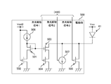
- FIG. 5 is a diagram showing a configuration example of a drive unit according to the embodiment of the present disclosure.
- the figure is a circuit diagram showing a configuration example of the drive unit 500.
- the drive unit 500 in the figure includes MOS transistors 501 to 505 and constant current circuits 506 and 507.
- the light source 41 is also shown in the figure.
- the light source 41 in the figure assumes a laser diode.
- Vdd2 in the figure is a power supply line that supplies power to the MOS transistors 501 to 503.
- Vcc is a power supply line that supplies power to the light source 41.
- An n-channel MOS transistor can be used for the MOS transistors 501 to 505.
- the light emission drive signal 1 is input to the gate of the MOS transistor 504.
- the drain of the MOS transistor 504 is connected to the source of the MOS transistor 503, and the source of the MOS transistor 504 is grounded.
- a light emitting drive signal 2 is input to the control terminal of the constant current circuit 507.
- the source side terminal of the constant current circuit 507 is grounded.
- the sink side terminal of the constant current circuit 507, the drain of the MOS transistor 503, and the drain of the MOS transistor 505 are commonly connected to the cathode of the light source 41.
- the anode of the light source 41 is connected to Vcc.
- a light emitting drive signal 3 is input to the gate of the MOS transistor 505.
- the source of the MOS transistor 505 is grounded.
- the gate of the MOS transistor 503 is connected to the gate of the MOS transistor 501, the drain of the MOS transistor 501, and the source side terminal of the constant current circuit 506.
- the sink side terminal of the constant current circuit 506 and the gate of the MOS transistor 502 are connected to Vdd2.
- the source of the MOS transistor 502 is grounded, and the drain of the MOS transistor 502 is connected to the source of the MOS transistor 501.
- the MOS transistor 504 is a MOS transistor that allows a light emitting current to flow through the light source 41.
- the MOS transistor 104 is controlled by the light emission drive signal 1.
- the emission current is a current for emitting a laser beam of a desired intensity, and is defined by a MOS transistor 503 connected in series with the MOS transistor 504.
- the MOS transistor 503 and the MOS transistor 501 are connected to a current mirror, and the same current as the current supplied by the constant current circuit 506 flows through the MOS transistor 503. Therefore, the light emitting current is defined by the current of the constant current circuit 506.
- the MOS transistor 502 is a MOS transistor arranged so that the source potential of the MOS transistor 501 is aligned with the source potential of the MOS transistor 503.
- the constant current circuit 507 is a circuit that supplies a bias current to the light source 41.
- the constant current circuit 507 includes a control terminal, and the on / off of the bias current is controlled by the light emission drive signal 2 input to the control terminal.
- This bias current is a current that is less than the light emission threshold value of the light source 41, and is a current that flows to speed up the response of the light source 41.
- the MOS transistor 505 is a MOS transistor that allows an auxiliary drive current to flow.
- the auxiliary drive current is a current superimposed on the light emitting current, and is a current that makes the rise of the light emitting current steep.
- An inductance component is present in the wiring of the light source 41. This inductance component slows the rise of the emission current. Therefore, it is possible to compensate for the delay in the rise due to the inductance component by applying a relatively high voltage to the light source 41 and passing the auxiliary drive current during the rise period of the emission current.
- the auxiliary drive current can be passed by grounding the cathode of the light source 41 with the MOS transistor 505.
- FIG. 6 is a diagram showing an example of driving a light source according to the embodiment of the present disclosure.
- the figure is a diagram showing an example of driving the light source 41 in the drive circuit 42, and is a diagram showing the relationship between the drive signal and the light emission current of the light source 41.
- “drive signal”, “delay drive signal 1", “delay drive signal 2”, “emission drive signal 1”, “emission drive signal 2” and “emission drive signal 3” are binarized. It represents the signal waveform.
- the drive signal corresponds to a period in which the value "1" causes a light emitting current to flow through the light source 41.
- the “current of the light source 41” in the figure represents the waveform of the current flowing through the laser diode constituting the light source 41.
- the drive signal in the figure is delayed by the first signal delay circuit 200 and the second signal delay circuit 300, and delay drive signals 1 and 2 are generated.
- the light emission drive signal generation unit 400 generates light emission drive signals 1 to 3 having the pulse width shown in the figure by the delay drive signals 1 and 2 and the drive signal, and supplies the light emission drive signals 1 to 3 to the drive unit 500.
- the constant current circuit 507 described with reference to FIG. 5 operates and a bias current flows.
- the MOS transistor 504 conducts and the light emission current starts to flow.
- the light emission drive signal 3 becomes a value "1”
- the MOS transistor 505 described with reference to FIG. 5 conducts, an auxiliary drive current flows, and the rise time of the light emission current is shortened.
- the broken line in the figure represents the current of the light source 41 when the auxiliary drive current is not passed. Due to the influence of the inductance component of the wiring of the light source 41, the rise of the light emitting current is delayed.
- the delay time of the first signal delay circuit 200 and the second signal delay circuit 300 changes, the delay time of the light emission drive signals 1 to 3 with respect to the drive signal changes, and the light emission delay time of the light source 41 changes. Therefore, the accuracy of the distance measurement is lowered. It is necessary to adjust the delay time of the changed first signal delay circuit 200 and the like.
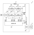
- FIG. 7 is a diagram showing a configuration example of a delay correction circuit according to the embodiment of the present disclosure.
- the figure is a diagram showing a configuration example of the delay correction circuit 100.
- the delay correction circuit 100 in the figure is adjusted by adjusting the reference delay circuit 110, the reference delay circuit power supply unit 120, the phase comparator 140, the delay adjustment unit 150, the calibration signal generation unit 160, and the reference delay adjustment unit 170.
- a result holding unit 180 and a reference delay adjustment result holding unit 190 are provided.
- the calibration signal generation unit 160 generates a calibration signal.
- a rectangular wave having a predetermined pulse width can be used for this calibration signal.
- the calibration signal generation unit 160 When adjusting the delay times of the first signal delay circuit 200 and the second signal delay circuit 300 to the reference delay time, the calibration signal generation unit 160 generates a calibration signal and described in the reference delay circuit 110 and FIG. Output to the receiving unit 600.
- the reference delay circuit 110 is a circuit that generates a reference delay time that serves as a reference for the delay time of the delay circuit arranged in the drive circuit 42.
- the reference delay circuit 110 in the figure generates the reference delay time of the first signal delay circuit 200 and the second signal delay circuit 300.
- the reference delay circuit 110 outputs a calibration signal delayed by a reference delay time with respect to the calibration signal input from the calibration signal generation unit 160.
- the reference delay circuit 110 can have the same configuration as the first signal delay circuit 200 described with reference to FIG. 2, for example. Details of the configuration of the reference delay circuit 110 will be described later.
- the reference delay circuit power supply unit 120 is a circuit that supplies power to the reference delay circuit 110.
- the reference delay circuit power supply unit 120 can be configured by a regulated power supply whose output voltage is calibrated.
- a regulated power supply for example, a bandgap reference power supply can be used.
- a regulated power supply it is possible to reduce the variation in the power supply voltage for each device, and it is possible to reduce the variation in the reference delay time for each device. Further, by using a regulated power supply, it is possible to reduce variations in the power supply voltage due to changes in the environmental temperature.
- gm changes and the delay time changes when the power supply voltage changes.
- the reference delay circuit 110 having the same configuration as the first signal delay circuit 200 also has a delay time that changes due to variations in the power supply voltage. Therefore, by arranging the reference delay circuit power supply unit 120 and supplying the reference delay circuit 110 with a power source having a small voltage variation, it is possible to reduce the fluctuation of the delay time of the reference delay circuit 110.
- a power supply whose voltage changes based on a predetermined temperature coefficient can be arranged in the reference delay circuit power supply unit 120.
- the delay time of the delay portion 210 and the like of the first signal delay circuit 200 increases as the temperature rises. Therefore, by increasing the power supply voltage when the temperature rises, it is possible to compensate for the change in the delay time.
- the power supply having a positive temperature coefficient in the reference delay circuit power supply unit 120 the fluctuation of the delay time of the reference delay circuit 110 can be further reduced. The details of the configuration of the reference delay circuit power supply unit 120 will be described later.
- the phase comparator 140 detects the phase difference by comparing the output signal of the reference delay circuit 110 with the light emission drive signal 2.
- the light emission drive signal 2 is a signal that has passed through the delay portions 310 and the like of all stages of the first signal delay circuit 200 and the second signal delay circuit 300.
- the calibration signal delayed by the first signal delay circuit 200 and the second signal delay circuit 300 is phased as the light emission drive signal 2. It is input to the comparator 140.
- the light emission drive signal 2 and the calibration signal delayed by the reference delay circuit 110 are compared by the phase comparator 140.
- the comparison result by the phase comparator 140 is output to the delay adjusting unit 150 and the reference delay adjusting unit 170.
- a known phase comparator can be used as the phase comparator 140.
- the delay adjustment unit 150 generates an adjustment signal and outputs it to the first signal delay circuit 200 and the second signal delay circuit 300, respectively. Further, the delay adjusting unit 150 generates an adjusting signal based on the comparison result of the phase comparator 140 during the adjusting processing of the first signal delay circuit 200 and the second signal delay circuit 300, and the first signal delay. The delay time of the circuit 200 and the second signal delay circuit 300 is adjusted.
- This adjustment can be performed as follows based on the comparison result from the phase comparator 140.
- the delay adjusting unit 150 shortens the delay time of the first signal delay circuit 200 and the second signal delay circuit 300. Specifically, the adjustment signal of the first signal delay circuit 200 is set to a lower value, and the adjustment signal of the second signal delay circuit 300 is set to a lower value.
- the delay adjusting unit 150 lengthens the delay time of the first signal delay circuit 200 and the second signal delay circuit 300.
- the adjustment signals of the first signal delay circuit 200 and the second signal delay circuit 300 are set to higher values. Adjustment can be performed by repeating this process until the output signal of the reference delay circuit 110 and the light emission drive signal 2 are synchronized. Thereby, the delay time of the first signal delay circuit 200 and the second signal delay circuit 300 can be made equal to the reference delay time.
- the adjustment result holding unit 180 holds the adjustment results of the first signal delay circuit 200 and the second signal delay circuit 300 after being adjusted by the delay adjusting unit 150.
- the adjustment result holding unit 180 can be configured by, for example, a memory that holds the value of the adjusted adjustment signal after adjustment.
- the delay adjustment unit 150 transfers and holds the adjustment results of the first signal delay circuit 200 and the second signal delay circuit 300 to the adjustment result holding unit 180. Further, the adjustment result holding unit 180 can supply the held adjustment result to the delay adjusting unit 150.
- the delay adjustment unit 150 can generate an adjustment signal based on the adjustment result supplied from the adjustment result holding unit 180 and output it to the first signal delay circuit 200 and the second signal delay circuit 300.
- the reference delay adjustment unit 170 generates and outputs an adjustment signal of the reference delay circuit 110. Further, the reference delay adjustment unit 170 controls the calibration signal generation unit 160 and the delay adjustment unit 150 during the above adjustment process.
- the reference delay adjustment unit 170 further adjusts the reference delay time.
- the reference delay adjusting unit 170 adjusts the reference delay time by adjusting the delay time of the reference delay circuit 110.
- the process of adjusting the delay time of the reference delay circuit 110 is referred to as a calibration process.
- the calibration process can be performed as follows. First, the reference delay adjustment unit 170 controls the delay adjustment unit 150 to output an adjustment signal, and sets the first signal delay circuit 200 and the second signal delay circuit 300 to a medium delay time. Next, the reference delay adjusting unit 170 causes the calibration signal generation unit 160 to output the calibration signal, and acquires the comparison result from the phase comparator 140.
- the reference delay adjusting unit 170 generates an adjustment signal based on the comparison result from the phase comparator 140, and adjusts the delay time of the reference delay circuit 110.
- the delay time of the reference delay circuit 110 is adjusted until the delay time of the reference delay circuit 110 becomes equal to the medium delay time of the first signal delay circuit 200 and the second signal delay circuit 300. As a result, the calibration process can be performed.
- the reference delay adjustment result holding unit 190 holds the adjustment result of the reference delay circuit 110 after adjustment by the reference delay adjustment unit 170.
- the reference delay adjustment result holding unit 190 can be configured by a memory that holds the value of the adjusted adjustment signal after adjustment.
- the reference delay adjustment unit 170 transfers the adjustment result of the reference delay circuit 110 to the reference delay adjustment result holding unit 190 and holds it. Further, the reference delay adjustment result holding unit 190 can supply the held adjustment result to the reference delay adjustment result holding unit 190.
- the reference delay adjustment unit 170 can generate an adjustment signal based on the adjustment result supplied from the reference delay adjustment result holding unit 190 and output it to the reference delay circuit 110.
- FIG. 8 is a diagram showing a configuration example of a reference delay circuit according to the embodiment of the present disclosure.
- the figure is a diagram showing a configuration example of the reference delay circuit 110.
- Power is supplied to the reference delay circuit 110 in the figure from the reference delay circuit power supply unit 120.
- Vdd3 in the figure represents a power supply line to which power is supplied from the reference delay circuit power supply unit 120.
- the reference delay circuit 110 in the figure includes an inverting gate 109, delay units 111 to 118, and a selection unit 119.
- the calibration signal generated by the calibration signal generation unit 160 is input to the reversing gate 109 in the figure.
- the delay portion 111 and the like in the figure can have the same configuration as the delay portion 210 and the like described in FIG.
- the reversing gate 109 and the selection unit 119 in the figure can have the same configuration as the reversing gate 201 and the selection unit 290 described in FIG.
- the delay section 111 and the like in the figure are different from the delay section 210 and the like in FIG. 2 in that power is supplied from the power supply line Vdd3. Since the power is supplied from the reference delay circuit power supply unit 120 to the delay unit 111 and the like, the variation in the delay time is reduced. Since the configuration of the reference delay circuit 110 other than this is the same as that of the first signal delay circuit 200, the description thereof will be omitted.
- FIG. 9 is a diagram showing a configuration example of a reference delay circuit power supply unit according to the embodiment of the present disclosure.
- the figure is a circuit diagram showing a configuration example of the reference delay circuit power supply unit 120.
- the reference delay circuit power supply unit 120 in the figure includes a transistor 122, resistors 124 to 128, a voltage source 121, a constant current circuit 123, a buffer amplifier 136, a temperature coefficient selection unit 130, and a temperature coefficient holding unit 135.
- An npn transistor can be used as the transistor 122.
- Vdd4 in the figure is a power supply line for supplying power for operating the reference delay circuit power supply unit 120.
- the collector of the transistor 122 is connected to Vdd4, and the emitter is connected to the sink side terminal of the constant current circuit 123.
- the source side terminal of the constant current circuit 123 is grounded.
- the base of the transistor 122 is connected to the high potential terminal of the voltage source 121, and the low potential terminal of the voltage source 121 is grounded.
- Resistors 124-128 connected in series are connected between the base and emitter of transistor 122.
- the plurality of signal lines 131 of the temperature coefficient selection unit 130 are connected to both ends of the resistors 124 to 128 connected in series and to each node to which the resistors are connected to each other. Further, the output of the temperature coefficient selection unit 130 is connected to the input of the buffer amplifier 136, and the output of the buffer amplifier 136 is connected to the reference delay circuit 110 as the output of the reference delay circuit power supply unit 120.
- the voltage source 121 is a voltage source corresponding to the above-mentioned regulated power supply.
- the voltage source 121 can be configured by, for example, a bandgap reference power supply.
- the constant current circuit 123 is a current source that supplies the emitter current of the transistor 122.
- the constant current circuit 123 supplies a sink current to the transistor 122.
- the resistors 124 to 128 are resistors that divide the base-emitter voltage Vbe of the transistor 122.
- the reference delay circuit power supply unit 120 in the figure shows an example in which Vbe is divided into five.
- the voltage of Vbe changes depending on the temperature coefficient of -2 mV / ° C.
- the temperature coefficient can be switched to a value of 0 to 2 mV / ° C. by connecting resistors 124 to 128 to divide the voltage.
- the circuit composed of the voltage source 121, the transistor 122, the constant current circuit 123, and the resistors 124 to 128 is an example of the temperature correction power supply according to the claims.
- the temperature coefficient selection unit 130 selects the temperature coefficient of the power supply output from the reference delay circuit power supply unit 120.
- the temperature coefficient selection unit 130 can select the temperature coefficient by selecting any one of the signal lines 131, extracting the voltage, and outputting the voltage to the buffer amplifier 136.
- the temperature coefficient holding unit 135 holds the selection result by the temperature coefficient selection unit 130.
- the temperature coefficient holding unit 135 can hold the selection result by holding the selection result of the signal line 131 by the temperature coefficient selection unit 130.
- the temperature coefficient selection unit 130 selects the signal line 131 based on the selection result held by the temperature coefficient holding unit 135.
- the temperature coefficient holding unit 135 can be configured by a memory.
- the buffer amplifier 136 is a buffer that amplifies the power supply voltage output from the temperature coefficient selection unit 130.
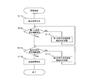
- FIG. 10 is a diagram showing an example of calibration processing according to the embodiment of the present disclosure.
- the reference delay adjustment unit 170 sets the initial values of the adjustment signals of the first signal delay circuit 200, the second signal delay circuit 300, and the reference delay circuit 110 (S101).
- the first signal delay circuit 200 and the second signal delay circuit 300 are performed by, for example, the reference delay adjustment unit 170 controlling the delay adjustment unit 150 so as to output an adjustment signal having a medium delay. Can be done.
- the first signal delay circuit 200 and the second signal delay circuit 300 can be set to a medium delay time.
- the reference delay circuit 110 can also be set to output an adjustment signal having a medium delay.
- the reference delay adjustment unit 170 can set the intermediate delay time by outputting the adjustment signal of the value "4" to the reference delay circuit 110, and can set the initial value.
- the calibration signal is output (S102). This can be done by the reference delay adjusting unit 170 controlling the calibration signal generation unit 160 to output the calibration signal.
- the reference delay adjusting unit 170 determines whether the adjustment of the reference delay circuit 110 is completed (S103). This is determined by the reference delay adjusting unit 170 based on the comparison result of the phase comparator 140. As a result of comparison by the phase comparator 140, when the phase difference between the output signal of the reference delay circuit 110 and the light emission drive signal 2 output from the light emission drive signal generation unit 400 is larger than a predetermined value, for example, 150 ps, the reference delay adjustment unit 170 can determine that the adjustment of the reference delay circuit 110 has not been completed (S103: No). In this case, the process proceeds to S104.
- a predetermined value for example 150 ps
- the reference delay adjustment unit 170 uses the reference delay adjustment unit 170 as a reference. It can be determined that the adjustment of the delay circuit 110 is completed (S103: Yes). In this case, the process proceeds to S105.
- the reference delay adjusting unit 170 adjusts the delay time of the reference delay circuit 110 (S104). This can be done by changing the adjustment signal of the reference delay circuit 110.
- the reference delay adjustment unit 170 sets the delay time of the reference delay circuit 110. increase. Specifically, the reference delay adjustment unit 170 generates and outputs an adjustment signal having a smaller value. For example, when the adjustment signal of the value "4" which is the medium delay time is generated, the adjustment signal of the value "2" which is the medium delay time is further generated and output. Twice
- the reference delay adjustment unit 170 delays the reference delay circuit 110. Reduce time. Specifically, the reference delay adjustment unit 170 generates and outputs an adjustment signal having a larger value. For example, when the adjustment signal of the value "4" is generated, the adjustment signal of the value "5" or "6" is generated and output. After that, the process of S103 is executed again.
- the reference delay adjusting unit 170 holds the calibration result (S105). This can be done by having the reference delay adjustment unit 170 hold the value of the adjustment signal in the reference delay adjustment result holding unit 190. After that, the calibration process is finished.
- the calibration process in the delay correction circuit 100 can be executed.
- This calibration process can be performed at the time of post-manufacturing inspection in the factory. In addition, it can be performed when the usage environment such as the place of use changes after the product is shipped.
- FIG. 11 is a diagram showing an example of the adjustment process according to the embodiment of the present disclosure.
- the calibration signal is output (S111). This can be done by the reference delay adjusting unit 170 controlling the calibration signal generation unit 160 to output the calibration signal.
- the delay adjusting unit 150 determines whether the adjustment of the first signal delay circuit 200 is completed (S112). This is determined by the delay adjusting unit 150 based on the comparison result of the phase comparator 140. As a result of comparison by the phase comparator 140, when the phase difference between the output signal of the reference delay circuit 110 and the light emission drive signal 2 output from the light emission drive signal generation unit 400 is larger than a predetermined value, for example, 100 ps, the delay adjustment unit 150 Can determine that the adjustment of the first signal delay circuit 200 has not been completed (S112: No). In this case, the process proceeds to S113.
- a predetermined value for example, 100 ps
- the delay adjustment unit 150 is set to the third. It can be determined that the adjustment of the signal delay circuit 200 of 1 is completed (S112: Yes). In this case, the process proceeds to S114.
- the delay adjusting unit 150 adjusts the delay time of the first signal delay circuit 200 (S113). This can be done by changing the adjustment signal of the first signal delay circuit 200.
- the delay adjustment unit 150 increases the delay time of the first signal delay circuit 200. Specifically, the delay adjustment unit 150 generates an adjustment signal having a smaller value and outputs it to the first signal delay circuit 200.
- the delay adjustment unit 150 reduces the delay time of the first signal delay circuit 200. Specifically, the delay adjustment unit 150 generates and outputs an adjustment signal having a larger value. After that, the process of S112 is executed again.
- S114 it is determined whether the adjustment of the second signal delay circuit 300 is completed (S114). This is determined by the delay adjusting unit 150 based on the comparison result of the phase comparator 140. As a result of comparison by the phase comparator 140, when the phase difference between the output signal of the reference delay circuit 110 and the light emission drive signal 2 is larger than a predetermined value, for example, 10 ps, the delay adjusting unit 150 of the second signal delay circuit 300 It can be determined that the adjustment has not been completed (S114: No). In this case, the process proceeds to S115.
- a predetermined value for example, 10 ps
- the delay adjusting unit 150 completes the adjustment of the second signal delay circuit 300. It can be determined that the signal has been processed (S114: Yes). In this case, the process proceeds to S116.
- the delay adjusting unit 150 adjusts the delay time of the second signal delay circuit 300 (S115). This can be done by changing the adjustment signal of the second signal delay circuit 300.
- the delay adjustment unit 150 increases the delay time of the second signal delay circuit 300.
- the delay adjustment unit 150 generates an adjustment signal having a smaller value and outputs it to the second signal delay circuit 300. For example, when the adjustment signal of the value "4" which is the medium delay time is generated, the adjustment signal of the value "2" which is the medium delay time is further generated and output.
- the delay adjustment unit 150 reduces the delay time of the second signal delay circuit 300. Specifically, the delay adjustment unit 150 generates an adjustment signal having a larger value and outputs it to the second signal delay circuit 300. For example, when the adjustment signal of the value "4" is generated, the adjustment signal of the value "5" or "6" which becomes the intermediate delay time is generated and output. After that, the process of S114 is executed again.
- the delay adjustment unit 150 holds the adjustment result (S116). This can be done by having the delay adjusting unit 150 hold the value of the adjustment signal in the adjustment result holding unit 180. After that, the adjustment process ends.
- the adjustment process in the delay correction circuit 100 can be executed.
- the process (S112) for adjusting the first signal delay circuit 200 corresponds to the rough adjustment of the delay time in the drive circuit 42.
- the process (S114) for adjusting the second signal delay circuit 300 corresponds to the fine adjustment of the delay time in the drive circuit 42.
- the reference delay circuit power supply unit 120 by arranging the reference delay circuit power supply unit 120 and supplying a highly stabilized power supply to the reference delay circuit 110, it is possible to reduce the variation in the delay time of the reference delay circuit 110.
- the delays of the first signal delay circuit 200 and the second signal delay circuit 300 are delayed.
- the time variation can be reduced.
- the delay time of the first signal delay circuit 200 and the like can also be provided. It is possible to reduce the variation of. However, in this case, the circuit scale of the drive circuit 42 becomes large.
- the first signal delay circuit 200 and the second signal delay circuit 300 need to be configured by a high-speed circuit. This is because such a high-speed circuit consumes a large amount of power and requires a large-capacity power supply circuit.
- the delay correction circuit 100 of the first embodiment of the present disclosure matches the delay times of the first signal delay circuit 200 and the second signal delay circuit 300 with the delay times of the reference delay circuit 110.
- the delay time of the first signal delay circuit 200 and the like is adjusted.
- the delay correction circuit 100 can be miniaturized.
- the drive circuit 42 of the first embodiment described above used the first signal delay circuit 200 and the second signal delay circuit 300.
- the drive circuit 42 of the second embodiment of the present disclosure uses a plurality of first signal delay circuits 200 and second signal delay circuits 300, respectively, in that the first embodiment described above is used. Different from the form.
- FIG. 12 is a diagram showing a configuration example of the light source device according to the second embodiment of the present disclosure. Similar to FIG. 1, FIG. 1 is a diagram showing a configuration example of the light source device 4. It differs from the light source device 4 described with reference to FIG. 1 in that two sets of the first signal delay circuit 200 and the second signal delay circuit 300 are arranged in the drive circuit 42, respectively.
- the drive circuit 42 in the figure is different from the drive circuit 42 in FIG. 1 in that it includes the first signal delay circuits 200a and 200b and the second signal delay circuits 300a and 300b.
- the first signal delay circuit 200a and the second signal delay circuit 300a generate the delay drive signal 1 described with reference to FIG. That is, the drive signal'is delayed to generate the delayed drive signal 1.
- the first signal delay circuit 200b and the second signal delay circuit 300b generate the delay drive signal 2 described with reference to FIG. That is, the drive signal'is delayed to generate the delayed drive signal 2. Therefore, even when the delay times of the delay drive signals 1 and 2 are significantly different, these signals can be generated.
- the delay correction circuit 100 in the figure generates and outputs the adjustment signals of the first signal delay circuits 200a and 200b and the second signal delay circuits 300a and 300b, respectively. During the adjustment process, the delay correction circuit 100 adjusts the first signal delay circuit 200a and the second signal delay circuit 300a and the first signal delay circuit 200b and the second signal delay circuit 300b. Do it individually.
- the configuration of the light source device 4 other than this is the same as the configuration of the light source device 4 described in the first embodiment of the present disclosure, the description thereof will be omitted.
- the light source device 4 of the second embodiment of the present disclosure includes two sets of the first signal delay circuit 200 and the second signal delay circuit 300, and sets the delay time of each delay circuit. It is adjusted by one reference delay circuit 110. Thereby, the increase in the circuit scale of the drive circuit 42 can be reduced.
- the technology according to the present disclosure can be applied to various products.
- the technique according to the present disclosure may be applied to a distance measuring device.
- the distance measuring device is a device that measures the distance to an object.
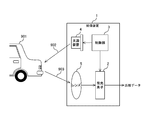
- FIG. 13 is a diagram showing a configuration example of an image pickup device according to a distance measuring device to which the technique according to the present disclosure can be applied.
- the figure is a block diagram showing a configuration example of the image pickup device 1 constituting the distance measuring device.
- the image pickup device 1 in the figure includes a light receiving element 2, a control unit 3, a light source device 4, and a lens 5.
- the object 901 for distance measurement is shown.
- the lens 5 is a lens that forms an image of an object on the light receiving element 2.
- the configuration of the light receiving element 2 will be described later. Twice
- the light source device 4 emits light to an object for distance measurement.
- a laser light source that emits infrared light can be used.
- the control unit 3 controls the entire image pickup apparatus 1. Specifically, the control unit 3 controls the light source device 4 to emit the emitted light 902 to the object 901, and notifies the light receiving element 2 of the start of the emission.
- the light receiving element 2 notified of the emission of the emitted light 902 detects the reflected light 903 from the object 901, measures the time from the emission of the emitted light 902 to the detection of the reflected light 903, and measures the time from the emission of the emitted light 902 to the detection of the reflected light 903, and the distance to the object 901. To measure.
- the measured distance is output to the outside of the image pickup apparatus 1 as distance data.
- FIG. 14 is a diagram showing a configuration example of a light receiving element according to a distance measuring device to which the technique according to the present disclosure can be applied.
- the light receiving element 2 in the figure includes a pixel array unit 21, a bias power supply unit 25, and a light receiving signal processing unit 26.
- the pixel array unit 21 is configured by arranging a plurality of pixels 22 having a photoelectric conversion unit that performs photoelectric conversion of incident light in a two-dimensional grid pattern.
- the pixel 22 detects the incident light and outputs the received light signal as the detection result.
- the photoelectric conversion unit for example, an APD (Avalanche Photo Diode) or a SPAD (Single Photon Avalanche diode) can be used.
- the SPAD is arranged in the pixel 22 as a photoelectric conversion unit.
- Signal lines 23 and 24 are connected to each pixel 22.
- the signal line 23 is a signal line that supplies the bias voltage of the pixel 22.
- the signal line 24 is a signal line that transmits a received signal from the pixel 22.
- the pixel array unit 21 in the figure describes an example in which the pixels 22 are arranged in 4 rows and 5 columns, the number of pixels 22 arranged in the pixel array unit 21 is not limited.
- the bias power supply unit 25 is a power supply that supplies a bias voltage to the pixel 22.
- the bias power supply unit 25 supplies a bias voltage via the signal line 23.
- the light receiving signal processing unit 26 processes the light receiving signals output from the plurality of pixels 22 arranged in the pixel array unit 21.
- the process of the received light signal processing unit 26 corresponds to, for example, a process of detecting the distance to the object based on the incident light detected by the pixel 22.
- the light receiving signal processing unit 26 can perform a ToF (Time of Flight) type distance detection process used when measuring a distance to a distant object in an imaging device such as an in-vehicle camera. ..
- the light source arranged in the image pickup apparatus irradiates the object with light, detects the light reflected by the object, and measures the time for the light from the light source to reciprocate between the object and the object. This is a process of detecting the distance.
- SPAD capable of high-speed light detection is used.
- the technology according to the present disclosure can also be applied to devices other than the distance measuring device.
- it can be applied to a delay circuit for changing the sampling timing of an analog-to-digital converter.
- the processing procedure described in the above-described embodiment may be regarded as a method having these series of procedures, or as a program for causing a computer to execute these series of procedures or as a recording medium for storing the program. You may catch it.
- a recording medium for example, a CD (Compact Disc), a DVD (Digital Versatile Disc), a memory card, or the like can be used.
- the present technology can have the following configurations.
- a reference delay circuit that generates a reference delay time that serves as a reference for the delay time of the signal of the signal delay circuit that delays the signal.
- a phase comparator that compares the phase of the signal delayed by the signal delay circuit and the signal delayed by the reference delay circuit, and A delay adjusting unit that adjusts the delay time of the signal delay circuit based on the phase comparison result,
- a delay correction circuit including a reference delay circuit power supply unit that supplies power to the reference delay circuit.
- the reference delay circuit power supply unit includes a temperature correction power supply in which the output voltage changes based on a predetermined temperature coefficient.
- the signal delay circuit includes a plurality of delay circuits having different delay times.
- the delay correction circuit according to any one of (1) to (4), wherein the delay adjusting unit adjusts the delay times of the plurality of delay circuits.
- a signal delay circuit that delays the drive signal and A reference delay circuit that generates a reference delay time that serves as a reference for the delay time of the drive signal, and A phase comparator that compares the phase of the drive signal delayed by the signal delay circuit and the drive signal delayed by the reference delay circuit, and A delay adjusting unit that adjusts the delay time of the signal delay circuit based on the phase comparison result,
- a drive circuit including a reference delay circuit power supply unit that supplies power to the reference delay circuit.
Landscapes
- Physics & Mathematics (AREA)
- Nonlinear Science (AREA)
- Engineering & Computer Science (AREA)
- Computer Networks & Wireless Communication (AREA)
- General Physics & Mathematics (AREA)
- Radar, Positioning & Navigation (AREA)
- Remote Sensing (AREA)
- Pulse Circuits (AREA)
Abstract
遅延補正回路を小型化する。 遅延補正回路は、基準遅延回路と位相比較器と遅延調整部と基準遅延回路電源部とを具備する。基準遅延回路は、信号を遅延させる信号遅延回路のその信号の遅延時間の基準となる基準遅延時間を生成する。位相比較器は、信号遅延回路により遅延されたその信号とその基準遅延回路により遅延されたその信号との位相を比較する。遅延調整部は、位相の比較結果に基づいてその信号遅延回路の遅延時間を調整する。基準遅延回路電源部は、基準遅延回路に電源を供給する。
Description
本開示は、遅延補正回路および駆動回路に関する。詳しくは、遅延回路の遅延時間を補正する遅延補正回路および当該遅延補正回路を使用する駆動回路に関する。
従来、対象物までの距離を測定する測距装置のようにレーザダイオード等の光源を所定のタイミングにおいて駆動する装置が使用されている。この測距装置においては、光が対象物との間を往復する時間を計時することにより対象物までの距離を測定する。具体的には、測距装置の光源を駆動することにより光を出力する。この光が対象物により反射されて反射光となる。この反射光が測距装置の光センサにより検出される。この光の出力から反射光の検出までの時間が計時されて距離が算出される。このような測距装置においては、光源を駆動するタイミングを調整する必要がある。光の出力と反射光の検出動作とを同期させるためである。光源を駆動するタイミングを調整するために、光源の駆動信号を所定の期間遅延させる遅延回路が使用される。
この遅延回路の遅延時間には厳格な管理が必要となる。距離の測定精度を向上させるためである。遅延時間の管理は遅延時間を補正することにより行うことができる。例えば、複数の遅延素子が縦続接続されて構成された遅延回路の各遅延素子の遅延時間を設定する回路を備える測距システムが使用されている(例えば、特許文献1参照。)。
この測距システムにおいては、駆動信号の遅延時間を制御する第1および第2の遅延時間制御回路により駆動タイミングの補正が行われる。この第1および第2の遅延時間制御回路の遅延時間は、遅延同期ループ回路により所定の遅延時間に管理される。環境変動による遅延同期ループ回路の遅延時間の変化を防ぐため、基準クロック信号による遅延時間の補正が行われる。この補正は、DLL(Delay Locked Loop)により遅延同期ループ回路の遅延時間を基準クロック信号の周期に揃えることにより行われる。
上述の従来技術では、回路サイズが増加するという問題がある。DLLは基準クロック信号と遅延同期ループ回路を通過した基準クロック信号との位相差を検出する位相比較器および位相比較器の出力信号のうちの低周波信号を通過させるローパスフィルタが配置される。このローパスフィルタは、キャパシタ等の受動素子により構成され、比較的大きな専有面積に構成される。このため、上述の従来技術の遅延補正回路は回路サイズが増加するという問題がある。
本開示は、上述した問題点に鑑みてなされたものであり、遅延補正回路を小型化することを目的としている。
本開示は、上述の問題点を解消するためになされたものであり、その第1の態様は、信号を遅延させる信号遅延回路の上記信号の遅延時間の基準となる基準遅延時間を生成する基準遅延回路と、上記信号遅延回路により遅延された上記信号と上記基準遅延回路により遅延された上記信号との位相を比較する位相比較器と、上記位相の比較結果に基づいて上記信号遅延回路の遅延時間を調整する遅延調整部と、上記基準遅延回路に電源を供給する基準遅延回路電源部とを具備する遅延補正回路である。
また、この第1の態様において、上記基準遅延回路電源部は、出力電圧が所定の温度係数に基づいて変化する温度補正電源を備えてもよい。
また、この第1の態様において、上記基準遅延回路電源部は、上記所定の温度係数を選択する温度係数選択部をさらに備えてもよい。
また、この第1の態様において、上記基準遅延回路電源部は、上記温度係数選択部における選択結果を保持する温度係数保持部をさらに備えてもよい。
また、この第1の態様において、上記信号遅延回路は、遅延時間が異なる複数の遅延回路を備え、上記遅延調整部は、上記複数の遅延回路の遅延時間を調整してもよい。
また、この第1の態様において、上記遅延調整部における上記遅延の調整結果を保持する調整結果保持部をさらに具備してもよい。
また、この第1の態様において、上記基準遅延時間を調整する基準遅延調整部をさらに具備してもよい。
また、この第1の態様において、上記基準遅延調整部における上記基準遅延時間の調整結果を保持する基準遅延調整結果保持部をさらに具備してもよい。
また、この第1の態様において、上記基準遅延調整部は、上記信号遅延回路の中位の遅延時間に上記基準遅延時間を調整してもよい。
また、本開示の第2の態様は、駆動信号を遅延させる信号遅延回路と、上記駆動信号の遅延時間の基準となる基準遅延時間を生成する基準遅延回路と、上記信号遅延回路により遅延された上記駆動信号と上記基準遅延回路により遅延された上記駆動信号との位相を比較する位相比較器と、上記位相の比較結果に基づいて上記信号遅延回路の遅延時間を調整する遅延調整部と、上記基準遅延回路に電源を供給する基準遅延回路電源部とを具備する駆動回路である。
本開示の態様により、基準遅延回路電源部により電源が供給される基準遅延回路により信号遅延回路の遅延時間が調整されるという作用をもたらす。信号遅延回路への基準遅延回路電源部による電源の供給の削減が想定される。
次に、図面を参照して、本開示を実施するための形態(以下、実施の形態と称する)を説明する。以下の図面において、同一または類似の部分には同一または類似の符号を付している。また、以下の順序で実施の形態の説明を行う。
1.第1の実施の形態
2.第2の実施の形態
3.測距装置への応用例
1.第1の実施の形態
2.第2の実施の形態
3.測距装置への応用例
<1.第1の実施の形態>
[光源装置の構成]
図1は、本開示の第1の実施の形態に係る光源装置の構成例を示す図である。同図は、光源装置4の構成例を表す図である。この光源装置4は、光源41と、駆動回路42とを備える。
[光源装置の構成]
図1は、本開示の第1の実施の形態に係る光源装置の構成例を示す図である。同図は、光源装置4の構成例を表す図である。この光源装置4は、光源41と、駆動回路42とを備える。
光源41は、光を出射するものである。この光源41は、例えば、レーザダイオードにより構成することができる。
駆動回路42は、光源41を駆動する回路である。この駆動回路42は、光源41に発光電流を供給することにより光源41を駆動する。なお、発光電流とは、光源41を発光させるために光源41に流す電流である。駆動回路42は、外部の回路より供給される駆動信号に基づいて光源41を駆動する。駆動信号は、2本の線により構成される差動伝送線路を介して供給される。差動伝送線路においては、互いに逆相の駆動信号が2本の信号線により伝達される。この差動信号のインターフェイスには、例えば、LVDS(Low Voltage Differential Signaling)を採用することができる。
駆動回路42は、受信部600と、第1の信号遅延回路200と、第2の信号遅延回路300と、発光駆動信号生成部400と、駆動部500と、遅延補正回路100とを備える。
受信部600は、駆動信号を受信するものである。この受信部600は、差動信号に変換されて伝達された駆動信号を受信するものである。この受信部600は、受信した駆動信号をシングルエンドの駆動信号に変換し、第1の信号遅延回路200および発光駆動信号生成部400に対して出力する。また、受信部600は、後述する校正信号を受信して第1の信号遅延回路200等に出力する。
第1の信号遅延回路200は、受信部600から出力された駆動信号を所定の遅延時間だけ遅延させる回路である。この第1の信号遅延回路200は、遅延させた駆動信号を第2の信号遅延回路300に対して出力する。第1の信号遅延回路200の遅延時間は、後述する遅延補正回路100から出力される調整信号により調整される。第1の信号遅延回路200の遅延時間は、次に説明する第2の信号遅延回路300の遅延時間より長い時間となる。このため、調整の際の遅延時間の分解能が小さくなる。第1の信号遅延回路200における遅延時間の調整は、粗調整に該当する。第1の信号遅延回路200の構成の詳細については後述する。
第2の信号遅延回路300は、第1の信号遅延回路200から出力された駆動信号を所定の遅延時間だけ遅延させる回路である。この第2の信号遅延回路300は、遅延させた駆動信号を発光駆動信号生成部400に対して出力する。第2の信号遅延回路300の遅延時間は、後述する遅延補正回路100から出力される調整信号により調整される。第2の信号遅延回路300の遅延時間は、第1の信号遅延回路200の遅延時間より短く、分解能が高くなる。第2の信号遅延回路300における遅延時間の調整は、微調整に該当する。なお、第2の信号遅延回路300は、遅延時間が異なる2つの駆動信号(後述する遅延駆動信号1および遅延駆動信号2)を出力する。第2の信号遅延回路300の構成の詳細については後述する。
発光駆動信号生成部400は、受信部600および第2の信号遅延回路300から出力された駆動信号等から発光駆動信号を生成するものである。ここで、発光駆動信号は、後述する駆動部500の素子の駆動信号である。発光駆動信号生成部400により生成された駆動信号は、駆動部500および遅延補正回路100に対して出力される。発光駆動信号生成部400の構成の詳細については後述する。
駆動部500は、光源41に駆動電流を供給するものである。この駆動部500は、発光駆動信号生成部400により生成された発光駆動信号に基づいて駆動電流を供給する。駆動部500の構成の詳細については後述する。
遅延補正回路100は、第1の信号遅延回路200および第2の信号遅延回路300の遅延時間を補正するものである。この遅延補正回路100は、遅延時間の基準となる基準遅延時間を生成する基準遅延回路(後述する基準遅延回路110)を備え、第1の信号遅延回路200および第2の信号遅延回路300の遅延時間と基準遅延回路110の遅延時間とを比較することにより第1の信号遅延回路200および第2の信号遅延回路300の遅延時間を調整する。
具体的には、遅延補正回路100は、遅延時間の調整のための校正信号を生成し、受信部600を介して校正信号を第1の信号遅延回路200に入力する。その後、第1の信号遅延回路200および第2の信号遅延回路300により遅延された駆動信号に基づいて発光駆動信号生成部400により生成された発光駆動信号が遅延補正回路100に入力される。一方、遅延補正回路100は、校正信号を自身の基準遅延回路110に入力することにより、基準遅延時間だけ遅延させた校正信号を生成する。そして、遅延補正回路100は、入力された発光駆動信号と遅延させた校正信号とを比較し、第1の信号遅延回路200および第2の信号遅延回路300の遅延時間を調整して発光駆動信号を遅延させた校正信号に同期させる。これにより、第1の信号遅延回路200および第2の信号遅延回路300の遅延時間を基準遅延時間に調整することができる。
以下、第1の信号遅延回路200および第2の信号遅延回路300の遅延時間を調整する処理を調整処理と称する。なお、第1の信号遅延回路200および第2の信号遅延回路300の遅延時間の調整は、それぞれ個別に出力される調整信号により行う。遅延補正回路100の構成の詳細については後述する。なお、駆動信号は、請求の範囲に記載の信号の一例である。
[第1の信号遅延回路の構成]
図2は、本開示の実施の形態に係る第1の信号遅延回路の構成例を示す図である。同図は、第1の信号遅延回路200の構成例を表す図である。同図の第1の信号遅延回路200は、反転ゲート201と、遅延部210、遅延部220、遅延部230、遅延部240、遅延部250、遅延部260、遅延部270および遅延部280と、選択部290とを備える。
図2は、本開示の実施の形態に係る第1の信号遅延回路の構成例を示す図である。同図は、第1の信号遅延回路200の構成例を表す図である。同図の第1の信号遅延回路200は、反転ゲート201と、遅延部210、遅延部220、遅延部230、遅延部240、遅延部250、遅延部260、遅延部270および遅延部280と、選択部290とを備える。
反転ゲート201は、受信部600から出力された駆動信号を反転するゲートである。なお、受信部600から出力された駆動信号を以下「駆動信号'」と記載する。反転ゲート201の出力は、遅延部210、遅延部220、遅延部230、遅延部240、遅延部250、遅延部260、遅延部270および遅延部280に共通に入力される。
遅延部210、遅延部220、遅延部230、遅延部240、遅延部250、遅延部260、遅延部270および遅延部280は、駆動信号’を遅延させる回路である。これら遅延部210等は、同一の回路により構成され、縦続接続される。すなわち、遅延部210の出力が遅延部220の入力に接続され、遅延部220の出力が遅延部230の入力に接続される。以下順に接続され、遅延部280の出力が第1の信号遅延回路200の出力となって第2の信号遅延回路300に接続される。なお、遅延部210の入力は接地されて値「0」が入力される。
遅延部210を例に挙げて回路構成を説明する。遅延部210は、2入力NORゲート211および212と、反転ゲート213とを備える。NORゲート211の入力には、信号線209および信号線291aが接続される。ここで、信号線209は、上述の反転ゲート201の出力信号を伝達する信号線である。信号線209から反転された駆動信号’がNORゲート211に入力される。信号線291aは、後述する選択部290からの選択信号を伝達する信号線である。NORゲート212の入力には、NORゲート211の出力および信号線219が接続される。なお、信号線219は、遅延部210の入力ノードに該当し、前段の遅延部の出力信号が入力されるノードである。上述のように、信号線219は接地されて値「0」が入力される。NORゲート212の出力は反転ゲート213の入力に接続され、反転ゲート213の出力は信号線229に接続される。なお、信号線229は、遅延部210の出力ノードに該当するとともに次段の遅延部の入力ノードに該当する。遅延部210等による1段当たりの遅延時間は、NORゲートおよび反転ゲートの遅延時間を加算したものとなり、100乃至150psとなる。
選択部290は、遅延補正回路100からの調整信号に基づいて遅延部210等のうちの1つを選択するものである。この選択部290は、複数の信号線291の何れか1つに選択信号を出力することにより遅延部210等の選択を行う。選択部290は、遅延部210等を選択することにより、第1の信号遅延回路200の遅延時間を調整する。選択部290は、選択した遅延部210等に接続される信号線291に値「0」を出力し、他の遅延部210等に値「1」を出力することにより、遅延部210等の選択を行う。
遅延部210が選択された場合を例に挙げて第1の信号遅延回路200の動作を説明する。選択部290は、信号線291aに値「0」を出力する。これにより、NORゲート211の出力には、信号線209を介して入力される反転された駆動信号’がさらに反転されて出力される。2入力NORゲート212の他の入力には信号線219を介して値「0」が入力されるため、NORゲート212の出力には、反転された駆動信号’が出力される。この反転された駆動信号’は、反転ゲート213により再度反転されて信号線229に出力され、遅延部220に入力される。遅延部220の信号線291bには、値「1」が選択部290より出力されているため、遅延部220のNORゲート221の出力は値「0」となり、遅延部220に入力された駆動信号’がNORゲート222および反転ゲート223を介して次段の遅延部230に出力される。以下、順に遅延部230から遅延部280までを経由して駆動信号’が伝達される。この場合、8段分の遅延時間を得ることができる。
遅延部220が選択された場合には、信号線291bに値「0」が出力される。駆動信号’は、遅延部220のNORゲート221を通過する。一方、選択されない遅延部210は、信号線219の信号を信号線229に出力する。信号線219には、値「0」が入力されているため、遅延部210は値「0」を信号線229に出力する。遅延部220の入力ノードには値「0」が入力され、NORゲート222に入力される。このため、駆動信号’は、遅延部220から遅延部280までを経由して伝達される。7段分の遅延時間となる。このように、選択部290により選択される遅延部210等の位置に応じて第1の信号遅延回路200の遅延時間を調整することができる。
遅延補正回路100からの調整信号には、例えば、3ビットのデジタル信号を使用することができる。この3ビットの調整信号により、遅延補正回路100は、第1の信号遅延回路200における遅延の段数を設定する。この遅延段数に応じた遅延部210等が選択部290により選択される。これにより、遅延補正回路100による第1の信号遅延回路200の遅延時間の調整を行うことができる。例えば、選択部290は、値「0」の調整信号が入力された際に遅延部210を選択し、値「7」の調整信号が入力された際に遅延部280を選択することができる。この場合、中位の遅延時間を第1の信号遅延回路200に設定する場合には、値「4」の調整信号を選択部290に入力することとなる。ここで中位の遅延時間とは、第1の信号遅延回路200等において設定可能な最大の遅延時間の略半分の遅延時間に相当する。
[第2の信号遅延回路の構成]
図3は、本開示の実施の形態に係る第2の信号遅延回路の構成例を示す図である。同図は、第2の信号遅延回路300の構成例を表す図である。なお、同図におけるAは第2の信号遅延回路300の回路図を表し、同図におけるBは第2の信号遅延回路300に使用される遅延部の構成例を表す回路図である。
図3は、本開示の実施の形態に係る第2の信号遅延回路の構成例を示す図である。同図は、第2の信号遅延回路300の構成例を表す図である。なお、同図におけるAは第2の信号遅延回路300の回路図を表し、同図におけるBは第2の信号遅延回路300に使用される遅延部の構成例を表す回路図である。
同図におけるAに表した第2の信号遅延回路300は、遅延部310、遅延部320、遅延部330、遅延部340、遅延部350、遅延部360、遅延部370および遅延部380と、選択部390とを備える。
遅延部310、遅延部320、遅延部330、遅延部340、遅延部350、遅延部360、遅延部370および遅延部380は、第1の信号遅延回路200から出力された駆動信号’を遅延させる回路である。前述の遅延部210等と同様に、これら遅延部310等は、同一の回路により構成され、縦続接続される。遅延部310等は、遅延時間を変更可能な反転ゲートにより構成される。遅延部310等には、選択部390からの選択信号を伝達するための信号線391がそれぞれ配線される。この選択信号により遅延部310等の遅延時間が変更される。例えば、値「1」の選択信号が入力された遅延部310等は長い遅延時間となり、値「0」の選択信号が入力された遅延部310等は短い遅延時間に変化する構成を採ることができる。
遅延部380の出力は、第2の信号遅延回路300の出力となり、第1の信号遅延回路200から出力された駆動信号’が全ての遅延部310等により遅延された信号である遅延駆動信号2が出力される。また、第2の信号遅延回路300は、一部の遅延部310等により遅延された信号である遅延駆動信号1をさらに出力する。遅延駆動信号1は、縦続接続された遅延部310等のうちの途中の段の遅延部の出力より得ることができる。同図におけるAは、遅延部340の出力から遅延駆動信号1が生成される例を表したものである。
選択部390は、遅延補正回路100からの調整信号に基づいて遅延部310等を選択するものである。この選択部390は、複数の信号線391に選択信号を出力することにより遅延部310等の選択を行う。選択部390は、遅延部310等を選択することにより、第2の信号遅延回路300の遅延時間を調整する。選択部390は、値「0」を選択信号として出力することができる。この場合、選択部390は、非選択の遅延部310等に値「1」を出力する。値「0」が選択信号として入力された遅延部310等は、短い遅延時間に変化する。このため、選択する遅延部310等の個数に応じて第2の信号遅延回路300の遅延時間を調整することができる。
遅延補正回路100からの調整信号には、例えば、3ビットのデジタル信号を使用することができる。この3ビットの調整信号により、遅延補正回路100は、第2の信号遅延回路300における遅延の段数を設定し、この遅延段数に応じた遅延部310等が選択部390により選択される。これにより、遅延補正回路100による第2の信号遅延回路300の遅延時間の調整を行うことができる。例えば、選択部390は、値「0」の調整信号が入力された際に全ての遅延部310等を非選択(値「1」を出力)とし、値「7」の調整信号が入力された際に全ての遅延部310を選択(値「0」を出力)することができる。この場合、中位の遅延時間を第2の信号遅延回路300に設定する場合には、値「4」の調整信号を選択部390に入力することとなる。
同図におけるBは、遅延部310等の構成を表す回路図である。遅延部310を例に挙げて説明する。遅延部310は、MOSトランジスタ311乃至316と、反転ゲート317とを備える。MOSトランジスタ311乃至313には、pチャネルMOSトランジスタを使用することができる。MOSトランジスタ314乃至316には、nチャネルMOSトランジスタを使用することができる。なお、Vdd1は、遅延部310の電源を供給する電源線である。信号線319および329は、それぞれ遅延部310の入力ノードおよび出力ノードに該当する信号線である。
MOSトランジスタ311のソース、MOSトランジスタ312のソースおよびMOSトランジスタ315のゲートは、Vdd1に接続される。MOSトランジスタ315のソース、MOSトランジスタ316のソースおよびMOSトランジスタ311のゲートは、接地される。MOSトランジスタ311のドレインは、MOSトランジスタ312のドレインおよびMOSトランジスタ313のソースに接続される。MOSトランジスタ312のゲートおよび反転ゲート317の入力は、信号線391に共通に接続される。反転ゲート317の出力は、MOSトランジスタ316のゲートに接続される。MOSトランジスタ316のドレインは、MOSトランジスタ315のドレインおよびMOSトランジスタ314のソースに接続される。MOSトランジスタ313のゲートおよびMOSトランジスタ314のゲートは、信号線319に共通に接続される。MOSトランジスタ313のドレインおよびMOSトランジスタ314のドレインは、信号線329に共通に接続される。
MOSトランジスタ313および314は、インバータを構成する。このMOSトランジスタ313および314からなるインバータには、並列に接続されたMOSトランジスタ311および312を介して電源電圧が供給され、並列に接続されたMOSトランジスタ315および316を介して接地される。MOSトランジスタ311のゲートは接地され、MOSトランジスタ315のゲートはVdd1に接続されるため、MOSトランジスタ311および315はオン状態になる。一方、MOSトランジスタ312のゲートは信号線391を介して選択信号が入力され、MOSトランジスタ316のゲートは反転ゲート317を介して選択信号が入力される。このため、値「0」の選択信号が入力されると、MOSトランジスタ312および316はオン状態になる。MOSトランジスタ312および316がオン状態になると、MOSトランジスタ313および314からなるインバータに供給される電源電圧が上昇し、MOSトランジスタ313および314のgmが高くなる。このため、MOSトランジスタ313および314が高速に動作して遅延時間が短くなる。これにより、1つの遅延部310の遅延時間を略10ps短くすることができる。
[発光駆動信号生成部の構成]
図4は、本開示の実施の形態に係る発光駆動信号生成部の構成例を示す図である。同図は、発光駆動信号生成部400の構成例を表す回路図である。同図の発光駆動信号生成部400は、反転ゲート401と、2入力ANDゲート402と、2入力ORゲート403と、非反転バッファ405乃至407とを備える。
図4は、本開示の実施の形態に係る発光駆動信号生成部の構成例を示す図である。同図は、発光駆動信号生成部400の構成例を表す回路図である。同図の発光駆動信号生成部400は、反転ゲート401と、2入力ANDゲート402と、2入力ORゲート403と、非反転バッファ405乃至407とを備える。
非反転バッファ405乃至407は、それぞれ発光駆動信号を出力するバッファである。この非反転バッファ405乃至407は、後述する駆動部のMOSトランジスタのゲートに信号を供給するバッファである。非反転バッファ405は発光駆動信号3を出力し、非反転バッファ406は発光駆動信号2を出力し、非反転バッファ407は発光駆動信号1を出力する。発光駆動信号1は、光源41に発光電流を流すための駆動信号である。発光駆動信号2は、光源41にバイアス電流を流すための駆動信号である。発光駆動信号3は、光源41の発光電流の立ち上がりを急峻にするための駆動信号である。
非反転バッファ405の入力には、遅延駆動信号2を反転させた信号と遅延駆動信号1とが論理積演算された信号が入力される。非反転バッファ406の入力には、遅延駆動信号1と駆動信号’とが論理和演算された信号が入力される。非反転バッファ407の入力には、遅延駆動信号1が入力される。発光駆動信号1および3は、駆動部500に対して出力される。また、発光駆動信号2は、駆動部500および後述する遅延補正回路100の位相比較器140に対して出力される。
[駆動部の構成]
図5は、本開示の実施の形態に係る駆動部の構成例を示す図である。同図は、駆動部500の構成例を表す回路図である。同図の駆動部500は、MOSトランジスタ501乃至505と、定電流回路506および507とを備える。また、同図には、光源41も記載した。同図の光源41は、レーザダイオードを想定したものである。同図のVdd2は、MOSトランジスタ501乃至503に電源を供給する電源線である。また、Vccは光源41に電源を供給する電源線である。MOSトランジスタ501乃至505には、nチャネルMOSトランジスタを使用することができる。
図5は、本開示の実施の形態に係る駆動部の構成例を示す図である。同図は、駆動部500の構成例を表す回路図である。同図の駆動部500は、MOSトランジスタ501乃至505と、定電流回路506および507とを備える。また、同図には、光源41も記載した。同図の光源41は、レーザダイオードを想定したものである。同図のVdd2は、MOSトランジスタ501乃至503に電源を供給する電源線である。また、Vccは光源41に電源を供給する電源線である。MOSトランジスタ501乃至505には、nチャネルMOSトランジスタを使用することができる。
MOSトランジスタ504のゲートには、発光駆動信号1が入力される。MOSトランジスタ504のドレインはMOSトランジスタ503のソースに接続され、MOSトランジスタ504のソースは接地される。定電流回路507の制御端子には、発光駆動信号2が入力される。定電流回路507のソース側端子は接地される。定電流回路507のシンク側端子、MOSトランジスタ503のドレインおよびMOSトランジスタ505のドレインは、光源41のカソードに共通に接続される。光源41のアノードは、Vccに接続される。MOSトランジスタ505のゲートには、発光駆動信号3が入力される。MOSトランジスタ505のソースは、接地される。MOSトランジスタ503のゲートは、MOSトランジスタ501のゲート、MOSトランジスタ501のドレインおよび定電流回路506のソース側端子に接続される。定電流回路506のシンク側端子およびMOSトランジスタ502のゲートは、Vdd2に接続される。MOSトランジスタ502のソースは接地され、MOSトランジスタ502のドレインはMOSトランジスタ501のソースに接続される。
MOSトランジスタ504は、光源41に発光電流を流すMOSトランジスタである。このMOSトランジスタ104は、発光駆動信号1により制御される。発光電流は、所望の強度のレーザ光を出射させるための電流であり、MOSトランジスタ504に直列に接続されたMOSトランジスタ503により規定される。MOSトランジスタ503およびMOSトランジスタ501はカレントミラー接続され、定電流回路506により供給される電流と同じ電流がMOSトランジスタ503に流れる。このため、発光電流は、定電流回路506の電流に規定される。なお、MOSトランジスタ502は、MOSトランジスタ501のソース電位をMOSトランジスタ503のソース電位に揃えるために配置されるMOSトランジスタである。
定電流回路507は、光源41にバイアス電流を供給する回路である。この定電流回路507は制御端子を備えており、制御端子に入力された発光駆動信号2によりバイアス電流のオンおよびオフが制御される。このバイアス電流は、光源41の発光閾値未満の電流であり、光源41の応答を高速化するために流す電流である。
MOSトランジスタ505は、補助駆動電流を流すMOSトランジスタである。ここで、補助駆動電流は、発光電流に重畳される電流であり、発光電流の立ち上がりを急峻にする電流である。光源41の配線にはインダクタンス成分が存在する。このインダクタンス成分により発光電流の立ち上がりが遅くなる。そこで、発光電流の立ち上がりの期間に光源41に比較的高い電圧を印加して補助駆動電流を流すことにより、インダクタンス成分による立ち上がりの遅れを補償することかできる。補助駆動電流は、MOSトランジスタ505により光源41のカソードを接地することにより流すことができる。
[駆動回路の動作]
図6は、本開示の実施の形態に係る光源の駆動の一例を示す図である。同図は、駆動回路42における光源41の駆動の一例を表す図であり、駆動信号と光源41の発光電流との関係を表す図である。同図において、「駆動信号」、「遅延駆動信号1」、「遅延駆動信号2」、「発光駆動信号1」、「発光駆動信号2」および「発光駆動信号3」は、2値化された信号波形を表したものである。駆動信号は、値「1」の期間が光源41に発光電流を流す期間に該当する。また、同図の「光源41の電流」は、光源41を構成するレーザダイオードを流れる電流の波形を表す。
図6は、本開示の実施の形態に係る光源の駆動の一例を示す図である。同図は、駆動回路42における光源41の駆動の一例を表す図であり、駆動信号と光源41の発光電流との関係を表す図である。同図において、「駆動信号」、「遅延駆動信号1」、「遅延駆動信号2」、「発光駆動信号1」、「発光駆動信号2」および「発光駆動信号3」は、2値化された信号波形を表したものである。駆動信号は、値「1」の期間が光源41に発光電流を流す期間に該当する。また、同図の「光源41の電流」は、光源41を構成するレーザダイオードを流れる電流の波形を表す。
同図の駆動信号が第1の信号遅延回路200および第2の信号遅延回路300により遅延されて遅延駆動信号1および2が生成される。発光駆動信号生成部400は、これら遅延駆動信号1および2と駆動信号とにより同図のパルス幅の発光駆動信号1乃至3を生成して駆動部500に供給する。
発光駆動信号2が値「1」になると、図5において説明した定電流回路507が動作し、バイアス電流が流れる。次に、発光駆動信号1が値「1」になると、MOSトランジスタ504が導通して発光電流が流れ始める。この際、発光駆動信号3が値「1」となり、図5において説明したMOSトランジスタ505が導通して補助駆動電流が流れ、発光電流の立ち上がり時間が短縮される。同図の破線は、補助駆動電流を流さない場合の光源41の電流を表したものである。光源41の配線のインダクタンス成分の影響により、発光電流の立ち上がりが遅くなる。
第1の信号遅延回路200および第2の信号遅延回路300の遅延時間が変化すると、駆動信号に対する発光駆動信号1乃至3の遅延時間が変化し、光源41の発光の遅延時間が変化する。このため、距離測定の精度が低下することとなる。この変化した第1の信号遅延回路200等の遅延時間の調整が必要になる。
[遅延補正回路の構成]
図7は、本開示の実施の形態に係る遅延補正回路の構成例を示す図である。同図は、遅延補正回路100の構成例を表す図である。同図の遅延補正回路100は、基準遅延回路110と、基準遅延回路電源部120と、位相比較器140と、遅延調整部150と、校正信号生成部160と、基準遅延調整部170と、調整結果保持部180と、基準遅延調整結果保持部190とを備える。
図7は、本開示の実施の形態に係る遅延補正回路の構成例を示す図である。同図は、遅延補正回路100の構成例を表す図である。同図の遅延補正回路100は、基準遅延回路110と、基準遅延回路電源部120と、位相比較器140と、遅延調整部150と、校正信号生成部160と、基準遅延調整部170と、調整結果保持部180と、基準遅延調整結果保持部190とを備える。
校正信号生成部160は、校正信号を生成するものである。この校正信号には、所定のパルス幅の矩形波を使用することができる。第1の信号遅延回路200および第2の信号遅延回路300の遅延時間を基準遅延時間に調整する際、校正信号生成部160は、校正信号を生成して基準遅延回路110および図1において説明した受信部600に出力する。
基準遅延回路110は、駆動回路42に配置された遅延回路の遅延時間の基準となる基準遅延時間を生成する回路である。同図の基準遅延回路110は、第1の信号遅延回路200および第2の信号遅延回路300の基準遅延時間を生成する。具体的には、基準遅延回路110は、校正信号生成部160から入力された校正信号に対して基準遅延時間だけ遅延させた校正信号を出力する。この基準遅延回路110は、例えば、図2において説明した第1の信号遅延回路200と同様の構成にすることができる。基準遅延回路110の構成の詳細については後述する。
基準遅延回路電源部120は、基準遅延回路110に電源を供給する回路である。基準遅延回路電源部120は、出力電圧が校正された安定化電源により構成することができる。この安定化電源には、例えば、バンドギャップリファレンス電源を使用することができる。安定化電源を使用することにより、装置毎の電源電圧のばらつきを低減することができ、装置毎の基準遅延時間のばらつきを低減することができる。また、安定化電源を使用することにより、環境温度の変化による電源電圧のばらつきを低減することもできる。第1の信号遅延回路200の遅延部210等は、電源電圧が変化するとgmが変化して遅延時間が変化する。第1の信号遅延回路200と同様の構成を採る基準遅延回路110も電源電圧のばらつきにより遅延時間が変化することとなる。そこで、基準遅延回路電源部120を配置して電圧のばらつきが小さい電源を基準遅延回路110に供給することにより、基準遅延回路110の遅延時間の変動を低減することができる。
また、所定の温度係数に基づいて電圧が変化する電源を基準遅延回路電源部120に配置することもできる。第1の信号遅延回路200の遅延部210等は、温度が上昇すると遅延時間が増大する。そこで、温度が上昇した際に電源電圧を上昇させることにより、遅延時間の変化を補償することができる。正の温度係数を有する電源を基準遅延回路電源部120に配置することにより、基準遅延回路110の遅延時間の変動をさらに低減することができる。基準遅延回路電源部120の構成の詳細については後述する。
位相比較器140は、基準遅延回路110の出力信号と発光駆動信号2とを比較して位相差を検出するものである。発光駆動信号2は、第1の信号遅延回路200および第2の信号遅延回路300の全段の遅延部310等を通過した信号である。受信部600を介して校正信号を第1の信号遅延回路200に入力することにより、第1の信号遅延回路200および第2の信号遅延回路300により遅延された校正信号が発光駆動信号2として位相比較器140に入力される。この発光駆動信号2と基準遅延回路110により遅延された校正信号とが位相比較器140により比較される。位相比較器140による比較結果は、遅延調整部150および基準遅延調整部170に出力される。なお、位相比較器140には、公知の位相比較器を使用することができる。
遅延調整部150は、調整信号を生成して第1の信号遅延回路200および第2の信号遅延回路300に対してそれぞれ出力するものである。また、遅延調整部150は、第1の信号遅延回路200および第2の信号遅延回路300の調整処理の際、位相比較器140の比較結果に基づいて調整信号を生成し、第1の信号遅延回路200および第2の信号遅延回路300の遅延時間を調整する。
この調整は、位相比較器140からの比較結果に基づいて、次のように行うことができる。基準遅延回路110の出力信号より発光駆動信号2が遅れている場合には、遅延調整部150は、第1の信号遅延回路200および第2の信号遅延回路300の遅延時間を短くする。具体的には、第1の信号遅延回路200の調整信号をより低い値に設定し、第2の信号遅延回路300の調整信号をより低い値に設定する。また、基準遅延回路110の出力信号より発光駆動信号2が進んでいる場合には、遅延調整部150は、第1の信号遅延回路200および第2の信号遅延回路300の遅延時間を長くする。具体的には、第1の信号遅延回路200および第2の信号遅延回路300の調整信号をより高い値に設定する。この処理を基準遅延回路110の出力信号および発光駆動信号2が同期するまで繰り返すことにより、調整を行うことができる。これにより、第1の信号遅延回路200および第2の信号遅延回路300の遅延時間を基準遅延時間に等しくすることができる。
調整結果保持部180は、遅延調整部150による調整後の第1の信号遅延回路200および第2の信号遅延回路300のそれぞれの調整結果を保持するものである。この調整結果保持部180は、例えば、調整後の調整信号の値を保持するメモリにより構成することができる。調整処理の後、遅延調整部150は、第1の信号遅延回路200および第2の信号遅延回路300のそれぞれの調整結果を調整結果保持部180に転送して保持させる。また、調整結果保持部180は、保持した調整結果を遅延調整部150に対して供給することができる。遅延調整部150は、調整結果保持部180から供給された調整結果に基づいて調整信号を生成し、第1の信号遅延回路200および第2の信号遅延回路300に対して出力することができる。
基準遅延調整部170は、基準遅延回路110の調整信号を生成して出力するものである。また、基準遅延調整部170は、上述の調整処理の際、校正信号生成部160および遅延調整部150の制御を行う。
また、基準遅延調整部170は、基準遅延時間の調整をさらに行う。基準遅延調整部170は、基準遅延回路110の遅延時間を調整することにより、基準遅延時間を調整する。以下、基準遅延回路110の遅延時間を調整する処理を校正処理と称する。校正処理は、次のように行うことができる。まず、基準遅延調整部170は、遅延調整部150を制御して調整信号を出力させ、第1の信号遅延回路200および第2の信号遅延回路300を中位の遅延時間に設定する。次に、基準遅延調整部170は、校正信号生成部160に校正信号を出力させて、位相比較器140からの比較結果を取得する。次に、基準遅延調整部170は、位相比較器140からの比較結果に基づいて調整信号を生成し、基準遅延回路110の遅延時間を調整する。基準遅延回路110の遅延時間が第1の信号遅延回路200および第2の信号遅延回路300の中位の遅延時間と等しくなるまで基準遅延回路110の遅延時間の調整を行う。これにより、校正処理を行うことができる。
基準遅延調整結果保持部190は、基準遅延調整部170による調整後の基準遅延回路110の調整結果を保持するものである。この基準遅延調整結果保持部190は、調整結果保持部180と同様に、調整後の調整信号の値を保持するメモリにより構成することができる。校正処理の後、基準遅延調整部170は、基準遅延回路110の調整結果を基準遅延調整結果保持部190に転送して保持させる。また、基準遅延調整結果保持部190は、保持した調整結果を基準遅延調整結果保持部190に対して供給することができる。上述の調整処理の際、基準遅延調整部170は、基準遅延調整結果保持部190から供給された調整結果に基づいて調整信号を生成し、基準遅延回路110に対して出力することができる。
[基準遅延回路の構成]
図8は、本開示の実施の形態に係る基準遅延回路の構成例を示す図である。同図は、基準遅延回路110の構成例を表す図である。同図の基準遅延回路110には、基準遅延回路電源部120から電源が供給される。同図のVdd3は、基準遅延回路電源部120からの電源が供給される電源線を表す。また、同図の基準遅延回路110は、反転ゲート109と、遅延部111乃至118と、選択部119とを備える。
図8は、本開示の実施の形態に係る基準遅延回路の構成例を示す図である。同図は、基準遅延回路110の構成例を表す図である。同図の基準遅延回路110には、基準遅延回路電源部120から電源が供給される。同図のVdd3は、基準遅延回路電源部120からの電源が供給される電源線を表す。また、同図の基準遅延回路110は、反転ゲート109と、遅延部111乃至118と、選択部119とを備える。
同図の反転ゲート109は、校正信号生成部160により生成された校正信号が入力される。同図の遅延部111等は図2において説明した遅延部210等と同様の構成を採ることができる。また、同図の反転ゲート109および選択部119は、図2において説明した反転ゲート201および選択部290と同様の構成を採ることができる。同図の遅延部111等は、電源線Vdd3から電源が供給される点で、図2の遅延部210等と異なる。遅延部111等に基準遅延回路電源部120からの電源が供給されるため、遅延時間のばらつきが低減される。これ以外の基準遅延回路110の構成は、第1の信号遅延回路200と同様であるため、説明を省略する。
[基準遅延回路電源部の構成]
図9は、本開示の実施の形態に係る基準遅延回路電源部の構成例を示す図である。同図は、基準遅延回路電源部120の構成例を表す回路図である。同図の基準遅延回路電源部120は、トランジスタ122と、抵抗124乃至128と、電圧源121と、定電流回路123と、バッファアンプ136と、温度係数選択部130と、温度係数保持部135とを備える。トランジスタ122には、npnトランジスタを使用することができる。なお、同図のVdd4は、基準遅延回路電源部120を動作させるための電源を供給する電源線である。
図9は、本開示の実施の形態に係る基準遅延回路電源部の構成例を示す図である。同図は、基準遅延回路電源部120の構成例を表す回路図である。同図の基準遅延回路電源部120は、トランジスタ122と、抵抗124乃至128と、電圧源121と、定電流回路123と、バッファアンプ136と、温度係数選択部130と、温度係数保持部135とを備える。トランジスタ122には、npnトランジスタを使用することができる。なお、同図のVdd4は、基準遅延回路電源部120を動作させるための電源を供給する電源線である。
トランジスタ122のコレクタはVdd4に接続され、エミッタは定電流回路123のシンク側端子に接続される。定電流回路123のソース側端子は、接地される。トランジスタ122のベースは電圧源121の高電位端子に接続され、電圧源121の低電位端子は接地される。直列に接続された抵抗124乃至128は、トランジスタ122のベースおよびエミッタの間に接続される。温度係数選択部130の複数の信号線131は、直列に接続された抵抗124乃至128の両端と抵抗同士が接続されるそれぞれのノードとに接続される。また、温度係数選択部130の出力はバッファアンプ136の入力に接続され、バッファアンプ136の出力は基準遅延回路電源部120の出力として基準遅延回路110に接続される。
電圧源121は、前述の安定化電源に相当する電圧源である。この電圧源121は、例えば、バンドギャップリファレンス電源により構成することができる。
定電流回路123は、トランジスタ122のエミッタ電流を供給する電流源である。この定電流回路123は、シンク電流をトランジスタ122に供給する。
抵抗124乃至128は、トランジスタ122のベースエミッタ間電圧Vbeを分圧する抵抗である。同図の基準遅延回路電源部120は、Vbeを5分割する例を表したものである。Vbeは、-2mV/℃の温度係数により電圧が変化する。このVbeを電圧源121の出力電圧から差し引くことにより、2mV/℃の温度係数に基づいて電圧が変化する電源回路を構成することができる。また、抵抗124乃至128を接続して分圧することにより、温度係数を0乃至2mV/℃の値に切り替えることができる。なお、電圧源121、トランジスタ122、定電流回路123および抵抗124乃至128により構成される回路は、請求の範囲に記載の温度補正電源の一例である。
温度係数選択部130は、基準遅延回路電源部120から出力される電源の温度係数を選択するものである。この温度係数選択部130は、信号線131の何れか1つを選択して電圧を取り出してバッファアンプ136に対して出力することにより、温度係数を選択することができる。
温度係数保持部135は、温度係数選択部130による選択結果を保持するものである。この温度係数保持部135は、温度係数選択部130による信号線131の選択結果を保持することにより、選択結果を保持することができる。温度係数選択部130は、温度係数保持部135に保持された選択結果に基づいて信号線131を選択する。温度係数保持部135は、メモリにより構成することができる。
バッファアンプ136は、温度係数選択部130から出力された電源電圧を増幅するバッファである。
[校正処理]
図10は、本開示の実施の形態に係る校正処理の一例を示す図である。まず、基準遅延調整部170が第1の信号遅延回路200、第2の信号遅延回路300および基準遅延回路110のそれぞれの調整信号の初期値を設定する(S101)。第1の信号遅延回路200および第2の信号遅延回路300については、例えば、中位の遅延とする調整信号を出力するように基準遅延調整部170が遅延調整部150を制御することにより行うことができる。前述のように、値「4」の調整信号を出力することにより、第1の信号遅延回路200および第2の信号遅延回路300を中位の遅延時間に設定することができる。また、基準遅延回路110についても、中位の遅延とする調整信号を出力するように設定することができる。基準遅延調整部170は、基準遅延回路110に対して値「4」の調整信号を出力することにより、中位の遅延時間に設定することができ、初期値を設定することができる。
図10は、本開示の実施の形態に係る校正処理の一例を示す図である。まず、基準遅延調整部170が第1の信号遅延回路200、第2の信号遅延回路300および基準遅延回路110のそれぞれの調整信号の初期値を設定する(S101)。第1の信号遅延回路200および第2の信号遅延回路300については、例えば、中位の遅延とする調整信号を出力するように基準遅延調整部170が遅延調整部150を制御することにより行うことができる。前述のように、値「4」の調整信号を出力することにより、第1の信号遅延回路200および第2の信号遅延回路300を中位の遅延時間に設定することができる。また、基準遅延回路110についても、中位の遅延とする調整信号を出力するように設定することができる。基準遅延調整部170は、基準遅延回路110に対して値「4」の調整信号を出力することにより、中位の遅延時間に設定することができ、初期値を設定することができる。
次に、校正信号を出力する(S102)。これは、基準遅延調整部170が校正信号生成部160を制御して校正信号を出力させることにより行うことができる。
次に、基準遅延回路110の調整が終了したかを判断する(S103)。これは、基準遅延調整部170が位相比較器140の比較結果に基づいて判断する。位相比較器140による比較の結果、基準遅延回路110の出力信号および発光駆動信号生成部400から出力される発光駆動信号2の位相差が所定の値、例えば、150psより大きい場合に基準遅延調整部170は、基準遅延回路110の調整が終了していないと判断することができる(S103:No)。この場合、S104の処理に移行する。
一方、基準遅延回路110の出力信号と発光駆動信号生成部400から出力される発光駆動信号2との位相差が上記所定の値(150ps)以下の場合には、基準遅延調整部170は、基準遅延回路110の調整が終了したと判断することができる(S103:Yes)。この場合、S105の処理に移行する。
S104において、基準遅延調整部170は、基準遅延回路110の遅延時間を調整する(S104)。これは、基準遅延回路110の調整信号を変更することにより行うことができる。発光駆動信号生成部400から出力される発光駆動信号2に対して基準遅延回路110の出力信号が進み位相となっている場合には、基準遅延調整部170は、基準遅延回路110の遅延時間を増加させる。具体的には、基準遅延調整部170は、より小さい値の調整信号を生成して出力する。例えば、中位の遅延時間である値「4」の調整信号が生成されていた場合には、さらに中位の遅延時間となる値「2」の調整信号を生成して出力する。
一方、発光駆動信号生成部400から出力される発光駆動信号2に対して基準遅延回路110の出力信号が遅れ位相となっている場合には、基準遅延調整部170は、基準遅延回路110の遅延時間を減少させる。具体的には、基準遅延調整部170は、より大きい値の調整信号を生成して出力する。例えば、値「4」の調整信号が生成されていた場合には、値「5」または「6」の調整信号を生成して出力する。その後、S103の処理を再度実行する。
S105において、基準遅延調整部170は、校正結果を保持する(S105)。これは、基準遅延調整部170が調整信号の値を基準遅延調整結果保持部190に保持させることにより行うことができる。その後、校正処理を終了する。
以上の手順により、遅延補正回路100における校正処理を実行することができる。この校正処理は、工場における製造後の検査時に行うことができる。また、製品として出荷された後において、使用場所等の使用環境が変わった際に行うことができる。
[調整処理]
図11は、本開示の実施の形態に係る調整処理の一例を示す図である。まず、校正信号を出力する(S111)。これは、基準遅延調整部170が校正信号生成部160を制御して校正信号を出力させることにより行うことができる。
図11は、本開示の実施の形態に係る調整処理の一例を示す図である。まず、校正信号を出力する(S111)。これは、基準遅延調整部170が校正信号生成部160を制御して校正信号を出力させることにより行うことができる。
次に、第1の信号遅延回路200の調整が終了したかを判断する(S112)。これは、遅延調整部150が位相比較器140の比較結果に基づいて判断する。位相比較器140による比較の結果、基準遅延回路110の出力信号および発光駆動信号生成部400から出力される発光駆動信号2の位相差が所定の値、例えば、100psより大きい場合に遅延調整部150は、第1の信号遅延回路200の調整が終了していないと判断することができる(S112:No)。この場合、S113の処理に移行する。
一方、基準遅延回路110の出力信号と発光駆動信号生成部400から出力される発光駆動信号2との位相差が上記の所定の値(100ps)以下の場合には、遅延調整部150は、第1の信号遅延回路200の調整が終了したと判断することができる(S112:Yes)。この場合、S114の処理に移行する。
S113において、遅延調整部150は、第1の信号遅延回路200の遅延時間を調整する(S113)。これは、第1の信号遅延回路200の調整信号を変更することにより行うことができる。基準遅延回路110の出力信号に対して発光駆動信号2が進み位相となっている場合には、遅延調整部150は、第1の信号遅延回路200の遅延時間を増加させる。具体的には、遅延調整部150は、より小さい値の調整信号を生成して第1の信号遅延回路200に対して出力する。
一方、基準遅延回路110の出力信号に対して発光駆動信号2が遅れ位相となっている場合には、遅延調整部150は、第1の信号遅延回路200の遅延時間を減少させる。具体的には、遅延調整部150は、より大きい値の調整信号を生成して出力する。その後、S112の処理を再度実行する。
S114において、第2の信号遅延回路300の調整が終了したかを判断する(S114)。これは、遅延調整部150が位相比較器140の比較結果に基づいて判断する。位相比較器140による比較の結果、基準遅延回路110の出力信号および発光駆動信号2の位相差が所定の値、例えば、10psより大きい場合に遅延調整部150は、第2の信号遅延回路300の調整が終了していないと判断することができる(S114:No)。この場合、S115の処理に移行する。
一方、基準遅延回路110の出力信号と発光駆動信号2との位相差が上記の所定の値(10ps)以下の場合には、遅延調整部150は、第2の信号遅延回路300の調整が終了したと判断することができる(S114:Yes)。この場合、S116の処理に移行する。
S115において、遅延調整部150は、第2の信号遅延回路300の遅延時間を調整する(S115)。これは、第2の信号遅延回路300の調整信号を変更することにより行うことができる。基準遅延回路110の出力信号に対して発光駆動信号2が進み位相となっている場合には、遅延調整部150は、第2の信号遅延回路300の遅延時間を増加させる。具体的には、遅延調整部150は、より小さい値の調整信号を生成して第2の信号遅延回路300に対して出力する。例えば、中位の遅延時間である値「4」の調整信号が生成されていた場合には、さらに中位の遅延時間となる値「2」の調整信号を生成して出力する。
一方、基準遅延回路110の出力信号に対して発光駆動信号2が遅れ位相となっている場合には、遅延調整部150は、第2の信号遅延回路300の遅延時間を減少させる。具体的には、遅延調整部150は、より大きい値の調整信号を生成して第2の信号遅延回路300に対して出力する。例えば、値「4」の調整信号が生成されていた場合には、さらに中位の遅延時間となる値「5」または「6」の調整信号を生成して出力する。その後、S114の処理を再度実行する。
S116において、遅延調整部150は、調整結果を保持する(S116)。これは、遅延調整部150が調整信号の値を調整結果保持部180に保持させることにより行うことができる。その後、調整処理を終了する。
以上の手順により、遅延補正回路100における調整処理を実行することができる。このうち、第1の信号遅延回路200を調整する処理(S112)は、駆動回路42における遅延時間の粗調整に該当する。また、第2の信号遅延回路300を調整する処理(S114)は、駆動回路42における遅延時間の微調整に該当する。このようにそれぞれ遅延時間が異なる第1の信号遅延回路200および第2の信号遅延回路300を配置して粗調整および微調整を個別に行うことにより、遅延時間の調整の精度を向上させることができるとともに調整に要する時間を短縮することができる。
前述のように、基準遅延回路電源部120を配置し、高度に安定化した電源を基準遅延回路110に供給することにより、基準遅延回路110の遅延時間のばらつきを低減することができる。この基準遅延回路110を使用して第1の信号遅延回路200および第2の信号遅延回路300の遅延時間を調整することにより、第1の信号遅延回路200および第2の信号遅延回路300の遅延時間のばらつきを低減することができる。基準遅延回路電源部120と同様の高性能電源回路をさらに配置して第1の信号遅延回路200および第2の信号遅延回路300に供給することによっても第1の信号遅延回路200等の遅延時間のばらつきを低減することは可能である。しかし、この場合には、駆動回路42の回路規模が大きくなる。伝達する駆動信号の波形の劣化等を防ぐため、第1の信号遅延回路200および第2の信号遅延回路300は高速な回路により構成する必要がある。このような高速な回路は消費電力が大きく、大容量の電源回路が必要になるためである。
以上説明したように、本開示の第1の実施の形態の遅延補正回路100は、第1の信号遅延回路200および第2の信号遅延回路300の遅延時間を基準遅延回路110の遅延時間に整合させることにより第1の信号遅延回路200等の遅延時間を調整する。これにより、遅延補正回路100を小型化することができる。
<2.第2の実施の形態>
上述の第1の実施の形態の駆動回路42は、第1の信号遅延回路200および第2の信号遅延回路300を使用していた。これに対し、本開示の第2の実施の形態の駆動回路42は、それぞれ複数の第1の信号遅延回路200および第2の信号遅延回路300を使用する点で、上述の第1の実施の形態と異なる。
上述の第1の実施の形態の駆動回路42は、第1の信号遅延回路200および第2の信号遅延回路300を使用していた。これに対し、本開示の第2の実施の形態の駆動回路42は、それぞれ複数の第1の信号遅延回路200および第2の信号遅延回路300を使用する点で、上述の第1の実施の形態と異なる。
[光源装置の構成]
図12は、本開示の第2の実施の形態に係る光源装置の構成例を示す図である。同図は、図1と同様に、光源装置4の構成例を表す図である。駆動回路42にそれぞれ2組の第1の信号遅延回路200および第2の信号遅延回路300が配置される点で、図1において説明した光源装置4と異なる。
図12は、本開示の第2の実施の形態に係る光源装置の構成例を示す図である。同図は、図1と同様に、光源装置4の構成例を表す図である。駆動回路42にそれぞれ2組の第1の信号遅延回路200および第2の信号遅延回路300が配置される点で、図1において説明した光源装置4と異なる。
同図の駆動回路42は、第1の信号遅延回路200aおよび200bならびに第2の信号遅延回路300aおよび300bを備える点で、図1の駆動回路42と異なる。第1の信号遅延回路200aおよび第2の信号遅延回路300aは、図6において説明した遅延駆動信号1を生成する。すなわち、駆動信号’を遅延させて遅延駆動信号1を生成する。一方、第1の信号遅延回路200bおよび第2の信号遅延回路300bは、図6において説明した遅延駆動信号2を生成する。すなわち、駆動信号’を遅延させて遅延駆動信号2を生成する。このため、遅延駆動信号1および2の遅延時間が大きく異なる場合であっても、これらの信号を生成することができる。
同図の遅延補正回路100は、第1の信号遅延回路200aおよび200bならびに第2の信号遅延回路300aおよび300bのそれぞれの調整信号を生成して出力する。調整処理の際には、遅延補正回路100は、第1の信号遅延回路200aおよび第2の信号遅延回路300aの調整と第1の信号遅延回路200bおよび第2の信号遅延回路300bの調整とを個別に行う。
これ以外の光源装置4の構成は本開示の第1の実施の形態において説明した光源装置4の構成と同様であるため、説明を省略する。
以上説明したように、本開示の第2の実施の形態の光源装置4は、2組の第1の信号遅延回路200および第2の信号遅延回路300を備え、それぞれの遅延回路の遅延時間を1つの基準遅延回路110により調整する。これにより、駆動回路42の回路規模の増大を軽減することができる。
<3.測距装置への応用例>
本開示に係る技術は、様々な製品へ応用することができる。例えば、本開示に係る技術は、測距装置に適用されてもよい。ここで、測距装置とは、対象物までの距離を測定する装置である。
本開示に係る技術は、様々な製品へ応用することができる。例えば、本開示に係る技術は、測距装置に適用されてもよい。ここで、測距装置とは、対象物までの距離を測定する装置である。
[撮像装置の構成]
図13は、本開示に係る技術が適用され得る測距装置に係る撮像装置の構成例を示す図である。同図は、測距装置を構成する撮像装置1の構成例を表すブロック図である。同図の撮像装置1は、受光素子2と、制御部3と、光源装置4と、レンズ5とを備える。なお、同図には、距離測定の対象物901を記載した。
図13は、本開示に係る技術が適用され得る測距装置に係る撮像装置の構成例を示す図である。同図は、測距装置を構成する撮像装置1の構成例を表すブロック図である。同図の撮像装置1は、受光素子2と、制御部3と、光源装置4と、レンズ5とを備える。なお、同図には、距離測定の対象物901を記載した。
レンズ5は、受光素子2に対象物を結像するレンズである。なお、受光素子2の構成については後述する。
光源装置4は、距離測定の対象物に光を出射するものである。この光源装置4は、例えば、赤外光を出射するレーザ光源を使用することができる。
制御部3は、撮像装置1の全体制御するものである。具体的には、制御部3は、光源装置4を制御して出射光902を対象物901に出射させるとともに、当該出射の開始を受光素子2に対して通知する。出射光902の出射が通知された受光素子2は、対象物901からの反射光903を検出して出射光902の出射から反射光903の検出までの時間を計測し、対象物901までの距離を測定する。この測定された距離は、距離データとして撮像装置1の外部に出力される。
[受光素子の構成]
図14は、本開示に係る技術が適用され得る測距装置に係る受光素子の構成例を示す図である。同図の受光素子2は、画素アレイ部21と、バイアス電源部25と、受光信号処理部26とを備える。
図14は、本開示に係る技術が適用され得る測距装置に係る受光素子の構成例を示す図である。同図の受光素子2は、画素アレイ部21と、バイアス電源部25と、受光信号処理部26とを備える。
画素アレイ部21は、入射光の光電変換を行う光電変換部を有する複数の画素22が2次元格子状に配置されて構成されたものである。この画素22は、入射光を検出し、受光信号を検出結果として出力する。光電変換部には、例えば、APD(Avalanche Photo Diode)やSPAD(Single Photon Avalanche diode)を使用することができる。以下、画素22には光電変換部としてSPADが配置されるものと想定する。それぞれの画素22には、信号線23および24が接続される。信号線23は、画素22のバイアス電圧を供給する信号線である。信号線24は、画素22からの受光信号を伝達する信号線である。なお、同図の画素アレイ部21には、画素22が4行5列に配置する例が記載されているが、画素アレイ部21に配置される画素22数を限定するものではない。
バイアス電源部25は、画素22にバイアス電圧を供給する電源である。このバイアス電源部25は、信号線23を介してバイアス電圧を供給する。
受光信号処理部26は、画素アレイ部21に配置される複数の画素22から出力された受光信号を処理するものである。この受光信号処理部26の処理には、例えば、画素22により検出した入射光に基づいて対象物との距離を検出する処理が該当する。具体的には、受光信号処理部26は、車載カメラ等の撮像装置において遠方の対象物との距離を計測する際に使用されるToF(Time of Flight)方式の距離検出処理を行うことができる。この距離検出処理は、撮像装置に配置された光源により対象物に光を照射して対象物により反射された光を検出し、光源からの光が対象物との間を往復する時間を計測することにより、距離を検出する処理である。このような距離検出処理を行う装置には、高速な光検出が可能なSPADが使用される。
なお、本開示に係る技術は、測距装置以外の装置に適用することもできる。例えば、アナログデジタル変換器のサンプリングタイミングを可変するための遅延回路に適用することができる。
最後に、上述した各実施の形態の説明は本開示の一例であり、本開示は上述の実施の形態に限定されることはない。このため、上述した各実施の形態以外であっても、本開示に係る技術的思想を逸脱しない範囲であれば、設計等に応じて種々の変更が可能であることは勿論である。
また、本明細書に記載された効果はあくまで例示であって限定されるものでは無い。また、他の効果があってもよい。
また、上述の実施の形態における図面は、模式的なものであり、各部の寸法の比率等は現実のものとは必ずしも一致しない。また、図面相互間においても互いの寸法の関係や比率が異なる部分が含まれることは勿論である。
また、上述の実施の形態において説明した処理手順は、これら一連の手順を有する方法として捉えてもよく、また、これら一連の手順をコンピュータに実行させるためのプログラム乃至そのプログラムを記憶する記録媒体として捉えてもよい。この記録媒体として、例えば、CD(Compact Disc)、DVD(Digital Versatile Disc)およびメモリカード等を用いることができる。
なお、本技術は以下のような構成もとることができる。
(1)信号を遅延させる信号遅延回路の前記信号の遅延時間の基準となる基準遅延時間を生成する基準遅延回路と、
前記信号遅延回路により遅延された前記信号と前記基準遅延回路により遅延された前記信号との位相を比較する位相比較器と、
前記位相の比較結果に基づいて前記信号遅延回路の遅延時間を調整する遅延調整部と、
前記基準遅延回路に電源を供給する基準遅延回路電源部と
を具備する遅延補正回路。
(2)前記基準遅延回路電源部は、出力電圧が所定の温度係数に基づいて変化する温度補正電源を備える前記(1)に記載の遅延補正回路。
(3)前記基準遅延回路電源部は、前記所定の温度係数を選択する温度係数選択部をさらに備える前記(2)に記載の遅延補正回路。
(4)前記基準遅延回路電源部は、前記温度係数選択部における選択結果を保持する温度係数保持部をさらに備える前記(3)に記載の遅延補正回路。
(5)前記信号遅延回路は、遅延時間が異なる複数の遅延回路を備え、
前記遅延調整部は、前記複数の遅延回路の遅延時間を調整する
前記(1)から(4)の何れかに記載の遅延補正回路。
(6)前記遅延調整部における前記遅延の調整結果を保持する調整結果保持部をさらに具備する前記(1)から(5)の何れかに記載の遅延補正回路。
(7)前記基準遅延時間を調整する基準遅延調整部をさらに具備する前記(1)から(6)の何れかに記載の遅延補正回路。
(8)前記基準遅延調整部における前記基準遅延時間の調整結果を保持する基準遅延調整結果保持部をさらに具備する前記(7)に記載の遅延補正回路。
(9)前記基準遅延調整部は、前記信号遅延回路の中位の遅延時間に前記基準遅延時間を調整する前記(7)に記載の遅延補正回路。
(10)駆動信号を遅延させる信号遅延回路と、
前記駆動信号の遅延時間の基準となる基準遅延時間を生成する基準遅延回路と、
前記信号遅延回路により遅延された前記駆動信号と前記基準遅延回路により遅延された前記駆動信号との位相を比較する位相比較器と、
前記位相の比較結果に基づいて前記信号遅延回路の遅延時間を調整する遅延調整部と、
前記基準遅延回路に電源を供給する基準遅延回路電源部と
を具備する駆動回路。
(1)信号を遅延させる信号遅延回路の前記信号の遅延時間の基準となる基準遅延時間を生成する基準遅延回路と、
前記信号遅延回路により遅延された前記信号と前記基準遅延回路により遅延された前記信号との位相を比較する位相比較器と、
前記位相の比較結果に基づいて前記信号遅延回路の遅延時間を調整する遅延調整部と、
前記基準遅延回路に電源を供給する基準遅延回路電源部と
を具備する遅延補正回路。
(2)前記基準遅延回路電源部は、出力電圧が所定の温度係数に基づいて変化する温度補正電源を備える前記(1)に記載の遅延補正回路。
(3)前記基準遅延回路電源部は、前記所定の温度係数を選択する温度係数選択部をさらに備える前記(2)に記載の遅延補正回路。
(4)前記基準遅延回路電源部は、前記温度係数選択部における選択結果を保持する温度係数保持部をさらに備える前記(3)に記載の遅延補正回路。
(5)前記信号遅延回路は、遅延時間が異なる複数の遅延回路を備え、
前記遅延調整部は、前記複数の遅延回路の遅延時間を調整する
前記(1)から(4)の何れかに記載の遅延補正回路。
(6)前記遅延調整部における前記遅延の調整結果を保持する調整結果保持部をさらに具備する前記(1)から(5)の何れかに記載の遅延補正回路。
(7)前記基準遅延時間を調整する基準遅延調整部をさらに具備する前記(1)から(6)の何れかに記載の遅延補正回路。
(8)前記基準遅延調整部における前記基準遅延時間の調整結果を保持する基準遅延調整結果保持部をさらに具備する前記(7)に記載の遅延補正回路。
(9)前記基準遅延調整部は、前記信号遅延回路の中位の遅延時間に前記基準遅延時間を調整する前記(7)に記載の遅延補正回路。
(10)駆動信号を遅延させる信号遅延回路と、
前記駆動信号の遅延時間の基準となる基準遅延時間を生成する基準遅延回路と、
前記信号遅延回路により遅延された前記駆動信号と前記基準遅延回路により遅延された前記駆動信号との位相を比較する位相比較器と、
前記位相の比較結果に基づいて前記信号遅延回路の遅延時間を調整する遅延調整部と、
前記基準遅延回路に電源を供給する基準遅延回路電源部と
を具備する駆動回路。
1 撮像装置
2 受光素子
4 光源装置
41 光源
42 駆動回路 100 遅延補正回路
110 基準遅延回路
111~118、210、220、230、240、250、260、270、280、310、320、330、340、350、360、370、380 遅延部
119、290、390 選択部
120 基準遅延回路電源部
121 電圧源
122 トランジスタ
123 定電流回路
124~128 抵抗
130 温度係数選択部
135 温度係数保持部
136 バッファアンプ
140 位相比較器
150 遅延調整部
160 校正信号生成部
170 基準遅延調整部
180 調整結果保持部
190 基準遅延調整結果保持部
200、200a、200b 第1の信号遅延回路
300、300a、300b 第2の信号遅延回路
400 発光駆動信号生成部
500 駆動部
600 受信部
2 受光素子
4 光源装置
41 光源
42 駆動回路 100 遅延補正回路
110 基準遅延回路
111~118、210、220、230、240、250、260、270、280、310、320、330、340、350、360、370、380 遅延部
119、290、390 選択部
120 基準遅延回路電源部
121 電圧源
122 トランジスタ
123 定電流回路
124~128 抵抗
130 温度係数選択部
135 温度係数保持部
136 バッファアンプ
140 位相比較器
150 遅延調整部
160 校正信号生成部
170 基準遅延調整部
180 調整結果保持部
190 基準遅延調整結果保持部
200、200a、200b 第1の信号遅延回路
300、300a、300b 第2の信号遅延回路
400 発光駆動信号生成部
500 駆動部
600 受信部
Claims (10)
- 信号を遅延させる信号遅延回路の前記信号の遅延時間の基準となる基準遅延時間を生成する基準遅延回路と、
前記信号遅延回路により遅延された前記信号と前記基準遅延回路により遅延された前記信号との位相を比較する位相比較器と、
前記位相の比較結果に基づいて前記信号遅延回路の遅延時間を調整する遅延調整部と、
前記基準遅延回路に電源を供給する基準遅延回路電源部と
を具備する遅延補正回路。 - 前記基準遅延回路電源部は、出力電圧が所定の温度係数に基づいて変化する温度補正電源を備える請求項1記載の遅延補正回路。
- 前記基準遅延回路電源部は、前記所定の温度係数を選択する温度係数選択部をさらに備える請求項2記載の遅延補正回路。
- 前記基準遅延回路電源部は、前記温度係数選択部における選択結果を保持する温度係数保持部をさらに備える請求項3記載の遅延補正回路。
- 前記信号遅延回路は、遅延時間が異なる複数の遅延回路を備え、
前記遅延調整部は、前記複数の遅延回路の遅延時間を調整する
請求項1記載の遅延補正回路。 - 前記遅延調整部における前記遅延の調整結果を保持する調整結果保持部をさらに具備する請求項1記載の遅延補正回路。
- 前記基準遅延時間を調整する基準遅延調整部をさらに具備する請求項1記載の遅延補正回路。
- 前記基準遅延調整部における前記基準遅延時間の調整結果を保持する基準遅延調整結果保持部をさらに具備する請求項7記載の遅延補正回路。
- 前記基準遅延調整部は、前記信号遅延回路の中位の遅延時間に前記基準遅延時間を調整する請求項7記載の遅延補正回路。
- 駆動信号を遅延させる信号遅延回路と、
前記駆動信号の遅延時間の基準となる基準遅延時間を生成する基準遅延回路と、
前記信号遅延回路により遅延された前記駆動信号と前記基準遅延回路により遅延された前記駆動信号との位相を比較する位相比較器と、
前記位相の比較結果に基づいて前記信号遅延回路の遅延時間を調整する遅延調整部と、
前記基準遅延回路に電源を供給する基準遅延回路電源部と
を具備する駆動回路。
Priority Applications (1)
| Application Number | Priority Date | Filing Date | Title |
|---|---|---|---|
| JP2022505795A JP7609846B2 (ja) | 2020-03-11 | 2021-01-13 | 遅延補正回路および駆動回路 |
Applications Claiming Priority (2)
| Application Number | Priority Date | Filing Date | Title |
|---|---|---|---|
| JP2020-042258 | 2020-03-11 | ||
| JP2020042258 | 2020-03-11 |
Publications (1)
| Publication Number | Publication Date |
|---|---|
| WO2021181857A1 true WO2021181857A1 (ja) | 2021-09-16 |
Family
ID=77671068
Family Applications (1)
| Application Number | Title | Priority Date | Filing Date |
|---|---|---|---|
| PCT/JP2021/000834 Ceased WO2021181857A1 (ja) | 2020-03-11 | 2021-01-13 | 遅延補正回路および駆動回路 |
Country Status (2)
| Country | Link |
|---|---|
| JP (1) | JP7609846B2 (ja) |
| WO (1) | WO2021181857A1 (ja) |
Citations (5)
| Publication number | Priority date | Publication date | Assignee | Title |
|---|---|---|---|---|
| JP2007267111A (ja) * | 2006-03-29 | 2007-10-11 | Nec Corp | クロック遅延補正回路 |
| JP2009236657A (ja) * | 2008-03-27 | 2009-10-15 | Panasonic Electric Works Co Ltd | 距離測定装置 |
| JP2011003088A (ja) * | 2009-06-19 | 2011-01-06 | Panasonic Corp | データラッチ調整装置およびそれを用いたメモリアクセスシステム |
| JP2013195307A (ja) * | 2012-03-21 | 2013-09-30 | Honda Motor Co Ltd | 測距システム |
| JP2014042314A (ja) * | 2007-11-29 | 2014-03-06 | Nlt Technologies Ltd | 可変遅延線及び可変遅延線を備えた表示装置及びシステム |
-
2021
- 2021-01-13 WO PCT/JP2021/000834 patent/WO2021181857A1/ja not_active Ceased
- 2021-01-13 JP JP2022505795A patent/JP7609846B2/ja active Active
Patent Citations (5)
| Publication number | Priority date | Publication date | Assignee | Title |
|---|---|---|---|---|
| JP2007267111A (ja) * | 2006-03-29 | 2007-10-11 | Nec Corp | クロック遅延補正回路 |
| JP2014042314A (ja) * | 2007-11-29 | 2014-03-06 | Nlt Technologies Ltd | 可変遅延線及び可変遅延線を備えた表示装置及びシステム |
| JP2009236657A (ja) * | 2008-03-27 | 2009-10-15 | Panasonic Electric Works Co Ltd | 距離測定装置 |
| JP2011003088A (ja) * | 2009-06-19 | 2011-01-06 | Panasonic Corp | データラッチ調整装置およびそれを用いたメモリアクセスシステム |
| JP2013195307A (ja) * | 2012-03-21 | 2013-09-30 | Honda Motor Co Ltd | 測距システム |
Also Published As
| Publication number | Publication date |
|---|---|
| JPWO2021181857A1 (ja) | 2021-09-16 |
| JP7609846B2 (ja) | 2025-01-07 |
Similar Documents
| Publication | Publication Date | Title |
|---|---|---|
| US11397249B2 (en) | Light detection device and electronic apparatus comprising a reverse bias voltage adjustment in accordance with a pulse number output by a first SPAD array | |
| JP6045963B2 (ja) | 光測距装置 | |
| US9866208B2 (en) | Precision measurements and calibrations for timing generators | |
| CN111458695B (zh) | 一种高速激光脉冲采样检测电路、系统及方法 | |
| US20100315119A1 (en) | Memory controller calibration | |
| US8976426B2 (en) | Light source driving circuit, optical scanning device, and image forming apparatus | |
| JP2018151197A (ja) | 距離計測装置および距離画像撮影装置 | |
| US8823575B2 (en) | Ad conversion circuit and solid-state image pickup device | |
| JPWO2020129954A1 (ja) | 測距撮像装置 | |
| US9035229B2 (en) | Imaging device | |
| JP7522045B2 (ja) | Dll回路及び測距撮像装置 | |
| WO2020100673A1 (ja) | 信号処理装置及び信号処理方法 | |
| WO2010035309A1 (ja) | 遅延回路およびそれを用いたタイミング発生器および試験装置 | |
| JP2020148682A (ja) | 距離測定装置及びスキュー補正方法 | |
| WO2022244656A1 (ja) | Tdc装置、測距装置および測距方法 | |
| JP7609846B2 (ja) | 遅延補正回路および駆動回路 | |
| US7701282B2 (en) | Offset canceling circuit and offset canceling method | |
| WO2021256094A1 (ja) | 光源駆動装置、光源装置および測距装置 | |
| US20230141571A1 (en) | Drive apparatus and distance measurement sensor including the same | |
| CN109412012B (zh) | 激光源产生电路及均衡方法 | |
| WO2020189137A1 (ja) | 電流生成回路および測距システム | |
| WO2021039933A1 (ja) | 測距システム、発光素子のドライバ | |
| US20260036694A1 (en) | Depth image sensing device and operation method thereof | |
| JP7488799B2 (ja) | 光検出装置、電子装置及び光検出方法 | |
| KR20230067474A (ko) | 구동 장치 및 이를 포함하는 거리 측정 센서 |
Legal Events
| Date | Code | Title | Description |
|---|---|---|---|
| 121 | Ep: the epo has been informed by wipo that ep was designated in this application |
Ref document number: 21768218 Country of ref document: EP Kind code of ref document: A1 |
|
| ENP | Entry into the national phase |
Ref document number: 2022505795 Country of ref document: JP Kind code of ref document: A |
|
| NENP | Non-entry into the national phase |
Ref country code: DE |
|
| 122 | Ep: pct application non-entry in european phase |
Ref document number: 21768218 Country of ref document: EP Kind code of ref document: A1 |