WO2021181644A1 - 半導体装置およびその製造方法 - Google Patents
半導体装置およびその製造方法 Download PDFInfo
- Publication number
- WO2021181644A1 WO2021181644A1 PCT/JP2020/010983 JP2020010983W WO2021181644A1 WO 2021181644 A1 WO2021181644 A1 WO 2021181644A1 JP 2020010983 W JP2020010983 W JP 2020010983W WO 2021181644 A1 WO2021181644 A1 WO 2021181644A1
- Authority
- WO
- WIPO (PCT)
- Prior art keywords
- semiconductor
- main surface
- semiconductor substrate
- region
- type
- Prior art date
- Legal status (The legal status is an assumption and is not a legal conclusion. Google has not performed a legal analysis and makes no representation as to the accuracy of the status listed.)
- Ceased
Links
Images





Classifications
-
- H—ELECTRICITY
- H10—SEMICONDUCTOR DEVICES; ELECTRIC SOLID-STATE DEVICES NOT OTHERWISE PROVIDED FOR
- H10P—GENERIC PROCESSES OR APPARATUS FOR THE MANUFACTURE OR TREATMENT OF DEVICES COVERED BY CLASS H10
- H10P95/00—Generic processes or apparatus for manufacture or treatments not covered by the other groups of this subclass
- H10P95/94—Hydrogenation or deuterisation, e.g. using atomic hydrogen from a plasma
-
- H—ELECTRICITY
- H10—SEMICONDUCTOR DEVICES; ELECTRIC SOLID-STATE DEVICES NOT OTHERWISE PROVIDED FOR
- H10D—INORGANIC ELECTRIC SEMICONDUCTOR DEVICES
- H10D12/00—Bipolar devices controlled by the field effect, e.g. insulated-gate bipolar transistors [IGBT]
- H10D12/01—Manufacture or treatment
- H10D12/031—Manufacture or treatment of IGBTs
- H10D12/032—Manufacture or treatment of IGBTs of vertical IGBTs
-
- H—ELECTRICITY
- H10—SEMICONDUCTOR DEVICES; ELECTRIC SOLID-STATE DEVICES NOT OTHERWISE PROVIDED FOR
- H10D—INORGANIC ELECTRIC SEMICONDUCTOR DEVICES
- H10D30/00—Field-effect transistors [FET]
- H10D30/01—Manufacture or treatment
- H10D30/021—Manufacture or treatment of FETs having insulated gates [IGFET]
- H10D30/028—Manufacture or treatment of FETs having insulated gates [IGFET] of double-diffused metal oxide semiconductor [DMOS] FETs
- H10D30/0291—Manufacture or treatment of FETs having insulated gates [IGFET] of double-diffused metal oxide semiconductor [DMOS] FETs of vertical DMOS [VDMOS] FETs
-
- H—ELECTRICITY
- H10—SEMICONDUCTOR DEVICES; ELECTRIC SOLID-STATE DEVICES NOT OTHERWISE PROVIDED FOR
- H10D—INORGANIC ELECTRIC SEMICONDUCTOR DEVICES
- H10D62/00—Semiconductor bodies, or regions thereof, of devices having potential barriers
- H10D62/10—Shapes, relative sizes or dispositions of the regions of the semiconductor bodies; Shapes of the semiconductor bodies
- H10D62/102—Constructional design considerations for preventing surface leakage or controlling electric field concentration
- H10D62/103—Constructional design considerations for preventing surface leakage or controlling electric field concentration for increasing or controlling the breakdown voltage of reverse-biased devices
- H10D62/105—Constructional design considerations for preventing surface leakage or controlling electric field concentration for increasing or controlling the breakdown voltage of reverse-biased devices by having particular doping profiles, shapes or arrangements of PN junctions; by having supplementary regions, e.g. junction termination extension [JTE]
- H10D62/109—Reduced surface field [RESURF] PN junction structures
- H10D62/111—Multiple RESURF structures, e.g. double RESURF or 3D-RESURF structures
-
- H—ELECTRICITY
- H10—SEMICONDUCTOR DEVICES; ELECTRIC SOLID-STATE DEVICES NOT OTHERWISE PROVIDED FOR
- H10D—INORGANIC ELECTRIC SEMICONDUCTOR DEVICES
- H10D62/00—Semiconductor bodies, or regions thereof, of devices having potential barriers
- H10D62/10—Shapes, relative sizes or dispositions of the regions of the semiconductor bodies; Shapes of the semiconductor bodies
- H10D62/129—Cathode regions of diodes
-
- H—ELECTRICITY
- H10—SEMICONDUCTOR DEVICES; ELECTRIC SOLID-STATE DEVICES NOT OTHERWISE PROVIDED FOR
- H10D—INORGANIC ELECTRIC SEMICONDUCTOR DEVICES
- H10D62/00—Semiconductor bodies, or regions thereof, of devices having potential barriers
- H10D62/10—Shapes, relative sizes or dispositions of the regions of the semiconductor bodies; Shapes of the semiconductor bodies
- H10D62/13—Semiconductor regions connected to electrodes carrying current to be rectified, amplified or switched, e.g. source or drain regions
- H10D62/141—Anode or cathode regions of thyristors; Collector or emitter regions of gated bipolar-mode devices, e.g. of IGBTs
- H10D62/145—Emitter regions of IGBTs
-
- H—ELECTRICITY
- H10—SEMICONDUCTOR DEVICES; ELECTRIC SOLID-STATE DEVICES NOT OTHERWISE PROVIDED FOR
- H10D—INORGANIC ELECTRIC SEMICONDUCTOR DEVICES
- H10D62/00—Semiconductor bodies, or regions thereof, of devices having potential barriers
- H10D62/10—Shapes, relative sizes or dispositions of the regions of the semiconductor bodies; Shapes of the semiconductor bodies
- H10D62/13—Semiconductor regions connected to electrodes carrying current to be rectified, amplified or switched, e.g. source or drain regions
- H10D62/149—Source or drain regions of field-effect devices
- H10D62/151—Source or drain regions of field-effect devices of IGFETs
- H10D62/156—Drain regions of DMOS transistors
- H10D62/157—Impurity concentrations or distributions
-
- H—ELECTRICITY
- H10—SEMICONDUCTOR DEVICES; ELECTRIC SOLID-STATE DEVICES NOT OTHERWISE PROVIDED FOR
- H10D—INORGANIC ELECTRIC SEMICONDUCTOR DEVICES
- H10D62/00—Semiconductor bodies, or regions thereof, of devices having potential barriers
- H10D62/50—Physical imperfections
- H10D62/53—Physical imperfections the imperfections being within the semiconductor body
-
- H—ELECTRICITY
- H10—SEMICONDUCTOR DEVICES; ELECTRIC SOLID-STATE DEVICES NOT OTHERWISE PROVIDED FOR
- H10D—INORGANIC ELECTRIC SEMICONDUCTOR DEVICES
- H10D62/00—Semiconductor bodies, or regions thereof, of devices having potential barriers
- H10D62/60—Impurity distributions or concentrations
-
- H—ELECTRICITY
- H10—SEMICONDUCTOR DEVICES; ELECTRIC SOLID-STATE DEVICES NOT OTHERWISE PROVIDED FOR
- H10D—INORGANIC ELECTRIC SEMICONDUCTOR DEVICES
- H10D62/00—Semiconductor bodies, or regions thereof, of devices having potential barriers
- H10D62/80—Semiconductor bodies, or regions thereof, of devices having potential barriers characterised by the materials
- H10D62/83—Semiconductor bodies, or regions thereof, of devices having potential barriers characterised by the materials being Group IV materials, e.g. B-doped Si or undoped Ge
- H10D62/834—Semiconductor bodies, or regions thereof, of devices having potential barriers characterised by the materials being Group IV materials, e.g. B-doped Si or undoped Ge further characterised by the dopants
-
- H—ELECTRICITY
- H10—SEMICONDUCTOR DEVICES; ELECTRIC SOLID-STATE DEVICES NOT OTHERWISE PROVIDED FOR
- H10D—INORGANIC ELECTRIC SEMICONDUCTOR DEVICES
- H10D8/00—Diodes
-
- H—ELECTRICITY
- H10—SEMICONDUCTOR DEVICES; ELECTRIC SOLID-STATE DEVICES NOT OTHERWISE PROVIDED FOR
- H10D—INORGANIC ELECTRIC SEMICONDUCTOR DEVICES
- H10D8/00—Diodes
- H10D8/01—Manufacture or treatment
- H10D8/045—Manufacture or treatment of PN junction diodes
-
- H—ELECTRICITY
- H10—SEMICONDUCTOR DEVICES; ELECTRIC SOLID-STATE DEVICES NOT OTHERWISE PROVIDED FOR
- H10D—INORGANIC ELECTRIC SEMICONDUCTOR DEVICES
- H10D12/00—Bipolar devices controlled by the field effect, e.g. insulated-gate bipolar transistors [IGBT]
- H10D12/411—Insulated-gate bipolar transistors [IGBT]
- H10D12/441—Vertical IGBTs
-
- H—ELECTRICITY
- H10—SEMICONDUCTOR DEVICES; ELECTRIC SOLID-STATE DEVICES NOT OTHERWISE PROVIDED FOR
- H10D—INORGANIC ELECTRIC SEMICONDUCTOR DEVICES
- H10D30/00—Field-effect transistors [FET]
- H10D30/60—Insulated-gate field-effect transistors [IGFET]
- H10D30/64—Double-diffused metal-oxide semiconductor [DMOS] FETs
- H10D30/66—Vertical DMOS [VDMOS] FETs
Definitions
- This disclosure relates to a semiconductor device and a method for manufacturing the same.
- the n-type drift layer of a power semiconductor device such as an IGBT (Insulated Gate Bipolar Transistor) using silicon (Si) as a semiconductor material is generally an FZ formed by crystal growth by the FZ (Floating Zone) method.
- a substrate is used.
- the FZ substrate is doped with phosphorus as an n-type dopant during crystal growth. If the specific resistance of the FZ substrate is too low, there will be a problem of reduced withstand voltage, and if it is too high, there will be a problem of reduced fracture endurance and oscillation such as ringing. In order to prevent the occurrence of these problems, it is effective to suppress the variation in the specific resistance of the n-type drift layer, and it is preferable to keep the tolerance of the specific resistance within the range of about ⁇ 10%.
- the substrate is uniformly irradiated (injected) with protons multiple times while shifting the range of the proton range by the distance obtained by dividing the half width of the proton range by an integer.
- the technology to make a donor is disclosed in.
- the technique can be carried out by, for example, an ion implantation device having an implantation energy of about 2 MeV, but in that case, the half width of the distribution of protons in silicon is as small as 10 ⁇ m or less, so that the number of times is considerable. Irradiation is required and the manufacturing cost increases.
- the present disclosure has been made in order to solve the above problems, and a semiconductor device and a method for manufacturing the same, which can obtain a uniform specific resistance of the n-type drift layer by a simple process in the manufacturing stage of the semiconductor device.
- the purpose is to provide.
- the semiconductor device is of a first conductive type formed between a semiconductor substrate having a first main surface and a second main surface and the first main surface and the second main surface of the semiconductor substrate.
- the first semiconductor region includes a second conductive type second semiconductor region formed between the first semiconductor region and the first main surface, and the first semiconductor region includes a hydrogen-related donor.
- the concentration of the hydrogen-related donor in the first semiconductor region is equal to or higher than the impurity concentration in the first semiconductor region.
- the shortage of donors is compensated by hydrogen-related donors by a simple process of penetrating a semiconductor substrate with light ions or electron beams at the manufacturing stage and performing hydrogen plasma treatment and annealing. It is possible to obtain a uniform specific resistance in the first semiconductor region which is an n-type drift layer.
- FIG. It is sectional drawing of the semiconductor device (PiN diode) which concerns on Embodiment 1.
- FIG. It is a figure which shows the dopant concentration profile in the depth direction of the semiconductor device which concerns on Embodiment 1.
- FIG. It is a flowchart which shows the manufacturing process of the semiconductor device which concerns on Embodiment 1.
- It is a schematic diagram of light ion irradiation to a semiconductor substrate.
- FIG. It is sectional drawing of the semiconductor device (IGBT) which concerns on Embodiment 2.
- FIG. It is sectional drawing of the semiconductor device (SJ-MOSFET) which concerns on Embodiment 3.
- FIG. It is a flowchart which shows the manufacturing process of the semiconductor device which concerns on Embodiment 3.
- FIG. 1 It is sectional drawing of the semiconductor substrate (SJ substrate) which concerns on Embodiment 3.
- FIG. It is a figure which shows the dopant concentration profile in the depth direction of the part of the p-pillar layer in the semiconductor substrate which concerns on Embodiment 3.
- FIG. It is a figure which shows the dopant concentration profile in the depth direction of the part of the n-pillar layer in the semiconductor substrate which concerns on Embodiment 3.
- FIG. It is a flowchart which shows the manufacturing process of the semiconductor device which concerns on Embodiment 4.
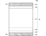
- FIG. 1 is a cross-sectional view showing the configuration of a PiN diode 100, which is a semiconductor device according to the first embodiment.
- FIG. 1 illustrates only the structure of the active region that operates as a diode, and omits the illustration of the terminal structure provided in the peripheral region outside the active region.
- the PiN diode 100 of the first embodiment is formed by using the semiconductor substrate 10 which is a silicon substrate (MCZ substrate) formed by the MCZ method.
- the type of the semiconductor substrate 10 is not limited to this, and for example, a silicon substrate (FZ substrate) formed by the FZ (Floating Zone) method may be used, or an epitaxial growth layer may be formed on the silicon substrate formed by the CZ (Czochralski) method.
- a CZ epi substrate formed by providing the above may be used.
- the type of the semiconductor substrate 10 those having characteristics suitable for the semiconductor device to be manufactured may be appropriately selected.
- the main surface on the front side (upper side in FIG. 1) of the semiconductor substrate 10 is defined as the first main surface 10a
- the main surface on the back side is defined as the second main surface 10b.
- the first conductive type will be described as n type
- the second conductive type will be described as p type.
- a first conductive type n-type drift layer 101 (first semiconductor region) is formed between the first main surface 10a and the second main surface 10b of the semiconductor substrate 10.
- a second conductive type p-type anode layer 102 (second semiconductor region) is formed between the surface layer portion on the first main surface 10a side of the semiconductor substrate 10, that is, the n-type drift layer 101 and the first main surface 10a. It is formed.
- the surface layer portion of the semiconductor substrate 10 on the second main surface 10b side, that is, between the n-type drift layer 101 and the second main surface 10b, is a first conductive type having a higher peak concentration of impurities than the n-type drift layer 101.
- N-type cathode layer 103 (third semiconductor region) is formed.
- the first conductive type has a higher peak concentration of impurities than the n-type drift layer 101 and a lower peak concentration of impurities than the n-type cathode layer 103.
- N-type buffer layer 104 is formed.
- anode electrode 105 connected to the p-type anode layer 102 is formed on the first main surface 10a of the semiconductor substrate 10.
- a cathode electrode 106 connected to the n-type cathode layer 103 is formed on the second main surface 10b of the semiconductor substrate 10.
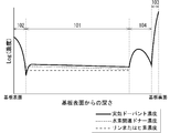
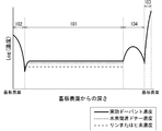
- FIG. 2 is a diagram showing a dopant concentration profile in the depth direction of the PiN diode 100, and is a dopant in the depth direction of the p-type anode layer 102, the n-type drift layer 101, the n-type buffer layer 104, and the n-type cathode layer 103.
- the concentration profile is shown.
- the n-type drift layer 101 is hydrogen-related over the entire area from the end of the first main surface 10a side (the substrate surface side) to the end of the second main surface 10b side (the substrate bottom surface side). Includes donors.
- the hydrogen-related donor concentration is always the impurity concentration (phosphorus) of the n-type drift layer 101 over the entire area from the end on the first main surface 10a side to the end on the second main surface 10b side. Or the concentration of arsenic) or more, and the concentration continuously increases from the second main surface 10b toward the first main surface 10a. That is, the hydrogen-related donor concentration of the n-type drift layer 101 is highest at the end of the n-type drift layer 101 on the first main surface 10a side, and highest at the end of the n-type drift layer 101 on the second main surface 10b side. Low.
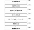
- FIG. 3 is a flowchart showing a manufacturing method of the PiN diode 100 according to the first embodiment. Hereinafter, a method of manufacturing the PiN diode 100 will be described with reference to FIG.
- step S101 a wafer of a semiconductor substrate 10 made of phosphorus-doped n-type silicon is prepared. At this time, the phosphorus concentration in the semiconductor substrate 10 is made lower than the phosphorus concentration for obtaining a desired withstand voltage in the completed semiconductor device, and the semiconductor substrate 10 is in a state of high resistivity.
- the n-type impurities doped in the semiconductor substrate 10 may be arsenic. Then, the element structure of the PiN diode 100 is formed on the first main surface 10a side of the semiconductor substrate 10.
- the p-type anode layer 102 is formed on the surface layer portion on the first main surface 10a side of the semiconductor substrate 10, and the anode electrode 105 connected to the p-type anode layer 102 is further formed on the first main surface 10a.
- the second main surface 10b of the semiconductor substrate 10 is ground so that the semiconductor substrate 10 has a desired thickness required for maintaining the withstand voltage. At this time, a process of removing the crushed layer by chemical etching grinding may be performed.
- step S103 In the back surface diffusion layer forming step (step S103), first, phosphorus is injected into the second main surface 10b of the semiconductor substrate 10 to form an n-type buffer layer 104 on the surface layer portion on the second main surface 10b side of the semiconductor substrate 10. Form. Further, an n-type cathode layer 103 having a higher peak concentration of impurities than the n-type buffer layer 104 is formed at a position shallower than the n-type buffer layer 104 on the surface layer portion on the second main surface 10b side of the semiconductor substrate 10. At this time, the second conductive type p-type cathode layer may be selectively formed on a part of the surface layer portion of the n-type cathode layer 103.
- the n-type region of the semiconductor substrate 10 remaining without forming the p-type anode layer 102, the n-type cathode layer 103, and the n-type buffer layer 104 in steps S101 and S103 becomes the n-type drift layer 101.
- the semiconductor substrate 10 is subjected to light ions 20 such as helium (He) from the second main surface 10b side of the semiconductor substrate 10 with an acceleration energy of 1 MeV or more.
- light ions 20 such as helium (He) from the second main surface 10b side of the semiconductor substrate 10 with an acceleration energy of 1 MeV or more.
- the semiconductor substrate 10 is in a state in which interstitial silicon (Si i ) deviating from the lattice position, vacancies (V; Vacancy) vacated at the lattice position, and the like are generated in the damaged region of the silicon.
- the light ion may be helium (He), hydrogen (H), or an isotope thereof, and the dose amount of light ion irradiation is 1 ⁇ 10 14 cm -2 or more and 1 ⁇ 10 16 cm -2 or less. It should be.
- step S105 In the hydrogen plasma irradiation / annealing step (step S105), first, hydrogen (H) is introduced into the damaged region of silicon by irradiating hydrogen plasma from the second main surface 10b side of the semiconductor substrate 10. Then, with hydrogen introduced into the damaged region, annealing is performed at 300 ° C. or higher and 450 ° C. or lower. As a result, the pores react with oxygen (O) contained in the wafer to form VO defects, and the VO defects react with hydrogen introduced by hydrogen plasma irradiation to form VOH defects.
- the VOH defect creates an electron trap level around 0.35 eV from the conduction band and also contributes to hydrogen-related donoring. As a result, hydrogen-related donors are formed in the entire region of the semiconductor substrate 10, and the dopant concentration profile shown in FIG. 2 is obtained.
- the cathode electrode 106 is formed on the second main surface 10b of the semiconductor substrate 10 as the back surface electrode required for packaging the package.
- the device wafer on which the PiN diode 100 having the configuration shown in FIG. 1 is formed is completed.
- the semiconductor in the manufacturing stage of the power device, the semiconductor is subjected to a simple process of penetrating light ions through the wafer of the semiconductor substrate 10 having high resistivity and performing hydrogen plasma treatment and annealing.
- a uniform resistivity of the n-type drift layer can be obtained. That is, the specific resistance of the wafer can be made uniform at the device manufacturing stage.
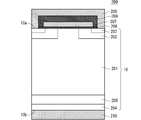
- FIG. 5 is a cross-sectional view showing the configuration of the IGBT 200, which is the semiconductor device according to the second embodiment. For the sake of simplicity, only the structure of the unit cell of the IGBT is shown in FIG. 5, and the termination structure provided in the peripheral region is not shown.
- MOS Metal Oxide Semiconductor
- the semiconductor substrate 10 on which the IGBT 200 is formed is assumed to be an MCZ substrate.
- the type of the semiconductor substrate 10 is not limited to this, and may be, for example, an FZ substrate, a CZ epi substrate, or the like.
- a first conductive type n-type drift layer 201 (first semiconductor region) is formed between the first main surface 10a and the second main surface 10b of the semiconductor substrate 10.
- the surface layer portion on the first main surface 10a side of the semiconductor substrate 10, that is, a part of the region between the n-type drift layer 201 and the first main surface 10a is a second conductive type p-type base layer 202 (the second conductive type p-type base layer 202). (2 semiconductor regions) are selectively formed.
- a first conductive type n-type emitter layer 203 is formed in a part of the surface layer portion of the p-type base layer 202.
- the surface layer portion of the semiconductor substrate 10 on the second main surface 10b side, that is, between the n-type drift layer 201 and the second main surface 10b, is a second conductive type having a higher peak concentration of impurities than the n-type drift layer 201.
- the p-type collector layer 204 (fourth semiconductor region) of the above is formed.
- the first conductive type has a higher peak concentration of impurities than the n-type drift layer 201 and a lower peak concentration of impurities than the p-type collector layer 204.
- N-type buffer layer 205 is formed.
- a gate insulating film 206 is formed on the first main surface 10a of the semiconductor substrate 10 so as to straddle the n-type drift layer 201, the p-type base layer 202, and the n-type emitter layer 203.
- the gate electrode 207 is formed in the gate electrode 207.
- the gate electrode 207 is arranged so as to face the n-type drift layer 201, the p-type base layer 202, and the n-type emitter layer 203 via the gate insulating film 206.
- An interlayer insulating film 208 is formed on the gate electrode 207, and an emitter electrode 209 is formed on the interlayer insulating film 208.
- a contact hole reaching the n-type emitter layer 203 is formed in the interlayer insulating film 208, and the emitter electrode 209 is connected to the n-type emitter layer 203 through the contact hole.
- a collector electrode 210 connected to the p-type collector layer 204 is formed on the second main surface 10b of the semiconductor substrate 10.
- the n-type drift layer 201 contains hydrogen-related donors over the entire area. Further, in the n-type drift layer 201, the hydrogen-related donor concentration is always equal to or higher than the impurity concentration (phosphorus or arsenic concentration) of the n-type drift layer 201 from the first main surface 10a side to the second main surface 10b side of the semiconductor substrate 10. It is continuously increasing from the second main surface 10b toward the first main surface 10a.
- the manufacturing method of the IGBT 200 of the second embodiment is basically represented by the same flowchart as in FIG.
- a method for manufacturing the IGBT 200 will be described with reference to FIG.
- step S101 a wafer of a semiconductor substrate 10 made of phosphorus-doped n-type silicon is prepared. At this time, the phosphorus concentration in the semiconductor substrate 10 is made lower than the phosphorus concentration for obtaining a desired withstand voltage in the completed semiconductor device, and the semiconductor substrate 10 is in a state of high resistivity.
- the n-type impurities doped in the semiconductor substrate 10 may be arsenic.
- the element structure of the IGBT 200 is formed on the first main surface 10a side of the semiconductor substrate 10. That is, the p-type base layer 202 and the n-type emitter layer 203 are formed on the surface layer portion on the first main surface 10a side of the semiconductor substrate 10.
- the gate insulating film 206, the gate electrode 207, the interlayer insulating film 208, and the emitter electrode 209 are formed on the first main surface 10a.
- the emitter electrode 209 is connected to the n-type emitter layer 203 through a contact hole formed in the interlayer insulating film 208.
- the second main surface 10b of the semiconductor substrate 10 is ground so that the semiconductor substrate 10 has a desired thickness required for maintaining the withstand voltage. At this time, a process of removing the crushed layer by chemical etching grinding may be performed.
- step S103 In the back surface diffusion layer forming step (step S103), first, phosphorus is injected into the second main surface 10b of the semiconductor substrate 10 to form an n-type buffer layer 205 on the surface layer portion on the second main surface 10b side of the semiconductor substrate 10. Form. Further, a p-type collector layer 204 having a higher peak concentration of impurities than the n-type buffer layer 205 is formed at a position shallower than the n-type buffer layer 205 on the surface layer portion on the second main surface 10b side of the semiconductor substrate 10.
- the n-type region of the semiconductor substrate 10 remaining without the p-type base layer 202, the n-type emitter layer 203, the p-type collector layer 204, and the n-type buffer layer 205 being formed is an n-type drift. It becomes layer 201.
- the semiconductor substrate 10 is subjected to light ions 20 such as helium (He) from the second main surface 10b side of the semiconductor substrate 10 with an acceleration energy of 1 MeV or more.
- light ions 20 such as helium (He) from the second main surface 10b side of the semiconductor substrate 10 with an acceleration energy of 1 MeV or more.
- step S105 In the hydrogen plasma irradiation / annealing step (step S105), first, hydrogen (H) is introduced into the damaged region of silicon by irradiating hydrogen plasma from the second main surface 10b side of the semiconductor substrate 10. Then, with hydrogen introduced into the damaged region, annealing is performed at 300 ° C. or higher and 450 ° C. or lower. As a result, hydrogen-related donors are formed in the entire region of the semiconductor substrate 10, and the dopant concentration profile of the n-type drift layer 201 described above can be obtained. That is, the hydrogen-related donor concentration is always higher than the phosphorus concentration in the entire n-type drift layer 201, and the hydrogen-related donor concentration continuously increases from the second main surface 10b to the first main surface 10a of the semiconductor substrate 10. The dopant concentration profile is obtained.
- a collector electrode 210 is formed on the second main surface 10b of the semiconductor substrate 10 as a back surface electrode required for packaging the package.
- the device wafer on which the IGBT 200 having the configuration shown in FIG. 5 is formed is completed.
- the IGBT 200 in FIG. 5 has a planar gate structure, it may have a trench gate structure.
- the gate insulating film 206 and the gate electrode 207 are formed in the trench formed on the first main surface 10a of the semiconductor substrate 10.
- the p-type base layer 202 and the n-type emitter layer 203 so that the gate electrode 207 in the trench faces the n-type drift layer 201, the p-type base layer 202, and the n-type emitter layer 203 via the gate insulating film 206.
- Is formed on the side wall of the trench, and the trench is formed at a depth at which the bottom reaches the n-type drift layer 201 below the p-type base layer 202.
- the semiconductor device of the second embodiment can be used as a MOSFET (Metal). It may be Oxide Semiconductor Field Effect Transistor). This MOSFET may also have a trench gate structure.
- the n-type collector layer may be partially formed together with the p-type collector layer 204 on the surface layer portion on the second main surface 10b side of the semiconductor substrate 10. That is, the p-type collector layer 204 and the n-type collector layer adjacent thereto may be formed between the n-type drift layer 201 and the second main surface 10b.
- an IGBT region and a diode region are provided on the first main surface 10a of the semiconductor substrate 10, and a p-type collector layer 204 is formed on the surface layer portion on the second main surface 10b side of the semiconductor substrate 10 in the IGBT region to form a diode region.
- the semiconductor device of the second embodiment may be an RC (Reverse-Conducting) type IGBT. That is, the p-type collector layer 204 and the n-type cathode layer adjacent thereto may be formed between the n-type drift layer 201 and the second main surface 10b.
- FIG. 6 is a cross-sectional view showing the configuration of the SJ-MOFSFET 300, which is the semiconductor device according to the third embodiment.
- FIG. 6 shows only the structure of the unit cell of the MOSFET, and omits the illustration of the terminal structure provided in the peripheral region.
- the semiconductor substrate 10 on which the SJ-MOFSFET 300 is formed is assumed to be a CZ epi substrate.
- the type of the semiconductor substrate 10 is not limited to this, and for example, the MCZ method, the FZ substrate, or the like may be used.
- a first conductive type n-type pillar layer 301 (first semiconductor pillar region) and a second conductive type
- the p-type pillar layer 302 (second semiconductor pillar region) is formed.
- the n-type pillar layer 301 and the p-type pillar layer 302 are adjacent to each other and are provided alternately in the lateral direction (the direction horizontal to the first main surface 10a).
- the surface layer portion on the first main surface 10a side of the semiconductor substrate 10, that is, a part of the region between the n-type pillar layer 301 and the p-type pillar layer 302 and the first main surface 10a is a second conductive type p.
- the mold base layer 303 is selectively formed. Further, a first conductive type n-type source layer 304 is formed in a part of the surface layer portion of the p-type base layer 303.
- the n-type pillar layer 301 and the p-type pillar layer 302 are located between the surface layer portion of the semiconductor substrate 10 on the second main surface 10b side, that is, the n-type pillar layer 301 and the p-type pillar layer 302 and the second main surface 10b.
- the first conductive type n-type drain layer 305 having a higher peak concentration of impurities is formed.
- a gate insulating film 306 is formed on the first main surface 10a of the semiconductor substrate 10 so as to straddle the n-type pillar layer 301, the p-type base layer 303, and the n-type source layer 304.
- a gate electrode 307 is formed in the gate electrode 307.
- the gate electrode 307 is arranged so as to face the n-type pillar layer 301, the p-type base layer 303, and the n-type source layer 304 via the gate insulating film 306.
- An interlayer insulating film 308 is formed on the gate electrode 307, and a source electrode 309 is formed on the interlayer insulating film 308.
- a contact hole reaching the n-type source layer 304 is formed in the interlayer insulating film 308, and the source electrode 309 is connected to the n-type source layer 304 through the contact hole.
- a drain electrode 310 connected to the n-type source layer 304 is formed on the second main surface 10b of the semiconductor substrate 10.
- the dopant concentration profile of the semiconductor substrate 10 in the third embodiment will be described later.
- FIG. 7 is a flowchart showing a manufacturing method of the SJ-MOFSFET 300 according to the third embodiment. Hereinafter, a method for manufacturing the SJ-MOFSFET 300 will be described with reference to FIG. 7.
- step S301 In the SJ substrate manufacturing step (step S301), first, as shown in FIG. 8, an n-type epitaxial layer 31 doped with phosphorus is grown on a high-concentration n-type substrate 30 doped with phosphorus or arsenic at a high concentration.
- a semiconductor substrate 10 which is a CZ epi substrate is prepared.
- the n-type pillar layer 301 and the p-type pillar layer 302 are formed in the n-type epitaxial layer 31 of the semiconductor substrate 10.
- the n-type pillar layer 301 and the p-type pillar layer 302 are adjacent to each other and are arranged alternately in the lateral direction.
- the semiconductor substrate 10 on which the n-type pillar layer 301 and the p-type pillar layer 302 are formed is referred to as an “SJ substrate 10”.
- the SJ substrate 10 may be manufactured by any method, for example, a multi-epi manufacturing method for forming an n-type pillar layer and a p-type pillar layer by repeating epitaxial growth and ion implantation a plurality of times, or a trench in a silicon layer.
- a trench fill method or the like for forming an n-type pillar layer and a p-type pillar layer by forming and epitaxially growing silicon so as to fill the trench can be used.
- the element structure of the SJ-MOFSFET 300 is formed on the first main surface 10a side of the semiconductor substrate 10.
- the p-type base layer 303 and the n-type source layer 304 are formed on the surface layer portion on the first main surface 10a side of the SJ substrate 10.
- a gate insulating film 306, a gate electrode 307, an interlayer insulating film 308, and a source electrode 309 are formed on the first main surface 10a.
- the source electrode 309 is connected to the n-type source layer 304 through a contact hole formed in the interlayer insulating film 308.
- the charge balance of the SJ substrate 10 is evaluated.
- the charge balance is evaluated by evaluating the element withstand voltage by a wafer test or by evaluating the TEG (Test Element Group) for the charge balance monitor.
- the TEG for the charge balance monitor may be a TEG formed on a monitor substrate different from the product wafer, or may be a TEG provided in an invalid region or a predetermined TEG area on the product wafer.
- the donor concentration and the acceptor concentration that are insufficient for the charge balance are calculated for the n-type pillar layer 301 and the p-type pillar layer 302.
- step S304 In the light ion irradiation step (step S304), as shown in FIG. 4, based on the calculation result of the shortage of the donor concentration in step S303, light helium (He) or the like is formed from the second main surface 10b side of the SJ substrate 10. By irradiating the ions 20 with an acceleration energy of 1 MeV or more so as to penetrate the semiconductor substrate 10, the entire silicon of the SJ substrate 10 is damaged.
- He light helium
- step S305 In the hydrogen plasma irradiation / annealing step (step S305), first, hydrogen (H) is introduced into the damaged region of silicon by performing hydrogen plasma irradiation from the second main surface 10b side of the SJ substrate 10. Then, with hydrogen introduced into the damaged region, annealing is performed at 300 ° C. or higher and 450 ° C. or lower. As a result, hydrogen-related donors are formed in the entire area of the SJ substrate 10. By adjusting the hydrogen-related donor concentration in this step, it is possible to evaluate the charge balance of the SJ substrate 10 and then correct the charge balance to a desired value.
- step S306 the high-concentration n-type substrate 30 on the second main surface 10b side of the SJ substrate 10 is ground in order to reduce the on-resistance of the SJ-MOFSFET 300. At this time, a process of removing the crushed layer by chemical etching grinding may be performed. The portion of the high-concentration n-type substrate 30 that remains without being removed in this step becomes the n-type drain layer 305.
- a drain electrode 310 is formed on the second main surface 10b of the SJ substrate 10 as a back surface electrode required for package sealing.
- the device wafer on which the IGBT 200 having the configuration shown in FIG. 6 is formed is completed.
- FIG. 9 shows a dopant concentration profile in the depth direction of the portion of the p-type pillar layer 302 in the SJ substrate 10 (FIG. 8) after the processes of steps S304 and S305, that is, along the A1-A2 line of FIG.
- the dopant concentration profile is shown.
- FIG. 10 the dopant concentration profile in the depth direction of the portion of the n-type pillar layer 301 in the SJ substrate 10 after the processing of steps S304 and S305, that is, the dopant concentration along the B1-B2 line of FIG. 8 Show profile.
- the concentration of the hydrogen-related donor introduced into the p-type pillar layer 302 is the p-type pillar layer over the entire range from the end on the first main surface 10a side to the end on the second main surface 10b side. It is always lower than the impurity concentration (boron concentration) of 302, and continuously increases from the second main surface 10b toward the first main surface 10a. That is, the concentration of hydrogen-related donors in the p-type pillar layer 302 is highest at the end of the p-type pillar layer 302 on the first main surface 10a side, and at the end of the p-type pillar layer 302 on the second main surface 10b side.
- the effective dopant concentration in the depth direction of the p-type pillar layer 302 is from the first main surface 10a side to the second main surface 10b side of the SJ substrate 10. The gradient becomes increasing.
- the concentration of the hydrogen-related donor introduced into the n-type pillar layer 301 is n-type over the entire range from the end on the first main surface 10a side to the end on the second main surface 10b side. It is always lower than the impurity concentration (phosphorus or arsenic concentration) of the pillar layer 301, and continuously increases from the second main surface 10b to the first main surface 10a. That is, the concentration of hydrogen-related donors in the n-type pillar layer 301 is also the highest at the end of the n-type pillar layer 301 on the first main surface 10a side, and at the end of the n-type pillar layer 301 on the second main surface 10b side.
- the effective dopant concentration in the depth direction of the n-type pillar layer 301 has a gradient that decreases from the first main surface 10a side to the second main surface 10b side of the SJ substrate 10.
- the SJ-MOFSFET 300 of the third embodiment has a structure in which the first main surface 10a side of the SJ substrate 10 is p-rich and gradually becomes n-rich toward the second main surface 10b of the SJ substrate 10.
- the sensitivity of the withstand voltage to the charge imbalance amount is increased and the peak withstand voltage can be increased, so that an effect that a higher withstand voltage can be secured can be obtained.
- the SJ-MOFSFET 300 in FIG. 6 has a planar gate structure, but may have a trench gate structure.
- the gate insulating film 306 and the gate electrode 307 are formed in the trench formed on the first main surface 10a of the SJ substrate 10.
- the p-type base layer 303 and the n-type source layer 304 so that the gate electrode 307 in the trench faces the n-type pillar layer 301, the p-type base layer 303, and the n-type source layer 304 via the gate insulating film 306. Is formed on the side wall of the trench, and the trench is formed at a depth at which the bottom reaches the n-type pillar layer 301 below the p-type base layer 303.
- the third embodiment may be an SJ-IGBT.
- This SJ-IGBT may also have a trench gate structure.
- the step of causing damage in the silicon of the semiconductor substrate 10 in order to introduce the hydrogen-related donor over the entire wafer is performed by electron beam irradiation instead of light ion irradiation.
- the electron beam is characterized by having higher permeability than light ions such as He and protons. Therefore, even if the electron beam is irradiated from the second main surface 10b of the wafer of the semiconductor substrate 10 as in FIG. 4, or the electron beam is irradiated from the first main surface 10a of the wafer contrary to FIG. 4, it is uniform. Damage can be caused. Therefore, the hydrogen-related donors introduced into the semiconductor substrate 10 are uniformly introduced in the depth direction of the semiconductor substrate 10.
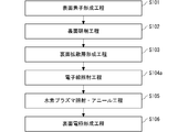
- FIG. 11 is a flowchart in the case of performing electron beam irradiation instead of light ion irradiation in the manufacturing method of the PiN diode 100 of the first embodiment.
- FIG. 11 shows that the light ion irradiation step (step S104) of FIG. 3 is replaced with the electron beam irradiation step (step S104a).
- the flow of FIG. 11 is basically the same as that of FIG. 3 except that electron beam irradiation is performed instead of light ion irradiation in step S104a.
- the irradiation energy of the electron beam is preferably in the range of 400 keV or more and 3 MeV or less.
- the electron beam may be irradiated from the first main surface 10a side of the semiconductor substrate 10 or from the second main surface 10b side.
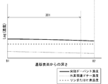
- the dopant concentration profile in the depth direction of the PiN diode 100 manufactured by the flow of FIG. 11 is shown in FIG. Similar to FIG. 2, the n-type drift layer 101 contains hydrogen-related donors over the entire area thereof, and the hydrogen-related donor concentration is always the impurity concentration (phosphorus or phosphorus or) of the n-type drift layer 101 over the entire area of the n-type drift layer 101. Arsenic concentration) or higher. However, unlike FIG. 2, the concentration of hydrogen-related donors in the depth direction of the semiconductor substrate 10 becomes uniform over the entire area of the n-type drift layer 101.
Landscapes
- Recrystallisation Techniques (AREA)
- Metal-Oxide And Bipolar Metal-Oxide Semiconductor Integrated Circuits (AREA)
- Physics & Mathematics (AREA)
- Engineering & Computer Science (AREA)
- Plasma & Fusion (AREA)
- Electrodes Of Semiconductors (AREA)
Abstract
Description
図1は、実施の形態1に係る半導体装置であるPiNダイオード100の構成を示す断面図である。簡単のため、図1には、ダイオードとして動作する活性領域の構造のみを図示し、活性領域の外側の周辺領域に設けられる終端構造の図示は省略している。
実施の形態2では、半導体基板10を用いて形成する半導体装置をMOS(Metal Oxide Semiconductor)型デバイスとした例を示す。図5は、実施の形態2に係る半導体装置であるIGBT200の構成を示す断面図である。簡単のため、図5には、IGBTのユニットセル分の構造のみを図示し、周辺領域に設けられる終端構造の図示は省略している。
実施の形態3では、半導体基板10を用いて形成する半導体装置をSJ(Super-Junction)タイプのMOS型デバイスとした例を示す。図6は、実施の形態3に係る半導体装置であるSJ-MOFSFET300の構成を示す断面図である。簡単のため、図6には、MOSFETのユニットセル分の構造のみを図示し、周辺領域に設けられる終端構造の図示は省略している。
実施の形態4では、ウエハ全域に水素関連ドナーを導入するために半導体基板10のシリコン中に損傷を生じさせる工程を、軽イオン照射ではなく、電子線照射によって行う。電子線は、Heやプロトン等の軽イオンに比べて透過性が高いという特徴がある。そのため、図4と同様に半導体基板10のウエハの第2主面10bから電子線を照射しても、図4とは逆にウエハの第1主面10aから電子線を照射しても、均一な損傷を生じさせることができる。そのため、半導体基板10に導入される水素関連ドナーは、半導体基板10の深さ方向に均一に導入される。
Claims (20)
- 第1主面および第2主面を有する半導体基板と、
前記半導体基板の前記第1主面と前記第2主面との間に形成された第1導電型の第1半導体領域と、
前記第1半導体領域と前記第1主面との間に形成された第2導電型の第2半導体領域と、
を備え、
前記第1半導体領域は水素関連ドナーを含み、
前記第1半導体領域の前記水素関連ドナーの濃度は、前記第1半導体領域の不純物濃度以上である、
半導体装置。 - 前記第1半導体領域の前記水素関連ドナーの濃度は、前記第2主面から前記第1主面に向かって連続的に増加している、
請求項1に記載の半導体装置。 - 前記第1半導体領域と前記第2主面との間に、前記第1半導体領域よりも不純物のピーク濃度が高い第1導電型の第3半導体領域を有する、
請求項1または請求項2に記載の半導体装置。 - 前記第1半導体領域と前記第2主面との間に、前記第1半導体領域よりも不純物のピーク濃度が高い第2導電型の第4半導体領域を備える、
請求項1または請求項2に記載の半導体装置。 - 前記第1半導体領域と前記第2主面との間に、第1導電型の第5半導体領域および前記第5半導体領域に隣接する第2導電型の第6半導体領域を備える、
請求項1または請求項2に記載の半導体装置。 - 前記半導体基板がMCZ基板である、
請求項1から請求項5のいずれか一項に記載の半導体装置。 - 第1主面および第2主面を有する半導体基板と、
前記半導体基板の前記第1主面と前記第2主面との間に形成され、前記第1主面に平行な方向に交互に配設された第1導電型の第1半導体ピラー領域および第2導電型の第2半導体ピラー領域と、
を備え、
前記第1半導体ピラー領域および前記第2半導体ピラー領域は水素関連ドナーを含み、
前記第1半導体ピラー領域および前記第2半導体ピラー領域の前記水素関連ドナーの濃度は、前記第1半導体ピラー領域の不純物濃度以下、且つ、前記第2半導体ピラー領域の不純物濃度以下である、
半導体装置。 - 前記第1半導体ピラー領域および前記第2半導体ピラー領域の前記水素関連ドナーの濃度は、前記第2主面から前記第1主面に向かって連続的に増加している、
請求項7に記載の半導体装置。 - 前記第1半導体ピラー領域および前記第2半導体ピラー領域と前記第2主面との間に、前記第1半導体ピラー領域および前記第2半導体ピラー領域よりも不純物のピーク濃度が高い第1導電型の半導体領域を有する、
請求項7または請求項8に記載の半導体装置。 - 前記第1半導体ピラー領域および前記第2半導体ピラー領域と前記第2主面との間に、前記第1半導体ピラー領域および前記第2半導体ピラー領域よりも不純物のピーク濃度が高い第2導電型の半導体領域を有する、
請求項7または請求項8に記載の半導体装置。 - リンまたはヒ素をドープした半導体基板の第1主面側に半導体装置の素子構造を形成する第1工程と、
前記半導体基板の第2主面側を研削する第2工程と、
前記半導体基板の前記第2主面側にn型またはp型の拡散層を形成する第3工程と、
軽イオンまたは電子線を前記半導体基板を貫通させるように照射する第4工程と、
前記半導体基板の前記第2主面に対して水素プラズマを照射してアニールを行う第5工程と、
前記半導体基板の第2主面上に電極を形成する第6工程と、
を備える半導体装置の製造方法。 - 前記軽イオンは、前記第2主面側から前記半導体基板に照射される、
請求項11に記載の半導体装置の製造方法。 - 前記軽イオンは、ヘリウムまたは水素、あるいはそれらの同位体である、
請求項11または請求項12に記載の半導体装置の製造方法。 - 前記軽イオンの照射の加速エネルギーは1MeV以上23MeV以下である、
請求項11または請求項12に記載の半導体装置の製造方法。 - 前記軽イオンの照射のドーズ量は、1×1014cm-2~1×1016cm-2である、
請求項13または請求項14に記載の半導体装置の製造方法。 - 前記第4工程において前記半導体基板には前記軽イオンが照射され、
前記アニールの温度は、300℃以上450℃以下である、
請求項11から請求項15のいずれか一項に記載の半導体装置の製造方法。 - 前記第4工程において前記半導体基板には前記軽イオンが照射され、
前記半導体基板の前記第1主面から前記第2主面にわたって、水素関連ドナーの濃度が前記半導体基板の不純物濃度以上になる、
請求項11から請求項16のいずれか一項に記載の半導体装置の製造方法。 - 前記半導体基板における前記水素関連ドナーの濃度が、前記第1主面から前記第2主面に向かって連続的に増加する、
請求項17に記載の半導体装置の製造方法。 - 前記第4工程において前記半導体基板には前記電子線が照射され、
前記電子線の照射の加速エネルギーは400keV~3MeVである、
請求項11に記載の半導体装置の製造方法。 - 前記第4工程において前記半導体基板には前記電子線が照射され、
前記半導体基板の前記第1主面から前記第2主面にわたって、水素関連ドナーの濃度が前記半導体基板の不純物濃度以上になる、
請求項11または請求項19に記載の半導体装置の製造方法。
Priority Applications (5)
| Application Number | Priority Date | Filing Date | Title |
|---|---|---|---|
| CN202080098195.1A CN115280471A (zh) | 2020-03-13 | 2020-03-13 | 半导体装置及其制造方法 |
| PCT/JP2020/010983 WO2021181644A1 (ja) | 2020-03-13 | 2020-03-13 | 半導体装置およびその製造方法 |
| JP2021531567A JP6976493B1 (ja) | 2020-03-13 | 2020-03-13 | 半導体装置およびその製造方法 |
| DE112020006883.8T DE112020006883T5 (de) | 2020-03-13 | 2020-03-13 | Halbleitereinheit und verfahren zur herstellung einer halbleitereinheit |
| US17/797,109 US12354878B2 (en) | 2020-03-13 | 2020-03-13 | Semiconductor device having semiconductor substrate including hydrogen-related donor, and manufacturing method therefor |
Applications Claiming Priority (1)
| Application Number | Priority Date | Filing Date | Title |
|---|---|---|---|
| PCT/JP2020/010983 WO2021181644A1 (ja) | 2020-03-13 | 2020-03-13 | 半導体装置およびその製造方法 |
Publications (1)
| Publication Number | Publication Date |
|---|---|
| WO2021181644A1 true WO2021181644A1 (ja) | 2021-09-16 |
Family
ID=77671054
Family Applications (1)
| Application Number | Title | Priority Date | Filing Date |
|---|---|---|---|
| PCT/JP2020/010983 Ceased WO2021181644A1 (ja) | 2020-03-13 | 2020-03-13 | 半導体装置およびその製造方法 |
Country Status (5)
| Country | Link |
|---|---|
| US (1) | US12354878B2 (ja) |
| JP (1) | JP6976493B1 (ja) |
| CN (1) | CN115280471A (ja) |
| DE (1) | DE112020006883T5 (ja) |
| WO (1) | WO2021181644A1 (ja) |
Cited By (1)
| Publication number | Priority date | Publication date | Assignee | Title |
|---|---|---|---|---|
| JP7466790B1 (ja) * | 2023-02-27 | 2024-04-12 | 三菱電機株式会社 | 半導体装置の製造方法 |
Families Citing this family (1)
| Publication number | Priority date | Publication date | Assignee | Title |
|---|---|---|---|---|
| CN113892185B (zh) * | 2019-12-18 | 2025-04-22 | 富士电机株式会社 | 半导体装置及半导体装置的制造方法 |
Citations (7)
| Publication number | Priority date | Publication date | Assignee | Title |
|---|---|---|---|---|
| JP2001326366A (ja) * | 2000-03-29 | 2001-11-22 | Sumiju Shiken Kensa Kk | 半導体素子の製造方法 |
| JP2004273863A (ja) * | 2003-03-10 | 2004-09-30 | Sansha Electric Mfg Co Ltd | 半導体ウエハの製造法 |
| JP2008258313A (ja) * | 2007-04-03 | 2008-10-23 | Denso Corp | 半導体装置およびその製造方法 |
| WO2013100155A1 (ja) * | 2011-12-28 | 2013-07-04 | 富士電機株式会社 | 半導体装置および半導体装置の製造方法 |
| JP2014093504A (ja) * | 2012-11-07 | 2014-05-19 | Sony Corp | 半導体装置、半導体装置の製造方法、及びアンテナスイッチモジュール |
| WO2014208404A1 (ja) * | 2013-06-26 | 2014-12-31 | 富士電機株式会社 | 半導体装置および半導体装置の製造方法 |
| WO2016204227A1 (ja) * | 2015-06-17 | 2016-12-22 | 富士電機株式会社 | 半導体装置および半導体装置の製造方法 |
Family Cites Families (7)
| Publication number | Priority date | Publication date | Assignee | Title |
|---|---|---|---|---|
| JP5228282B2 (ja) | 2006-03-28 | 2013-07-03 | トヨタ自動車株式会社 | 電力用半導体装置及びその製造方法 |
| JP5733417B2 (ja) * | 2011-11-15 | 2015-06-10 | 富士電機株式会社 | 半導体装置および半導体装置の製造方法 |
| US9012980B1 (en) * | 2013-12-04 | 2015-04-21 | Infineon Technologies Ag | Method of manufacturing a semiconductor device including proton irradiation and semiconductor device including charge compensation structure |
| DE102015114177A1 (de) | 2015-08-26 | 2017-03-02 | Infineon Technologies Ag | Halbleitervorrichtung, Siliziumwafer und Verfahren zum Herstellen eines Siliziumwafers |
| DE112018003666B4 (de) * | 2017-07-19 | 2025-02-06 | Mitsubishi Electric Corporation | Verfahren zur herstellung eines halbleiterbauelements und halbleiterbauelement |
| CN109712886A (zh) * | 2018-12-17 | 2019-05-03 | 成都森未科技有限公司 | 一种功率半导体器件的背面加工工艺 |
| US11450734B2 (en) * | 2019-06-17 | 2022-09-20 | Fuji Electric Co., Ltd. | Semiconductor device and fabrication method for semiconductor device |
-
2020
- 2020-03-13 US US17/797,109 patent/US12354878B2/en active Active
- 2020-03-13 WO PCT/JP2020/010983 patent/WO2021181644A1/ja not_active Ceased
- 2020-03-13 CN CN202080098195.1A patent/CN115280471A/zh active Pending
- 2020-03-13 JP JP2021531567A patent/JP6976493B1/ja active Active
- 2020-03-13 DE DE112020006883.8T patent/DE112020006883T5/de active Pending
Patent Citations (7)
| Publication number | Priority date | Publication date | Assignee | Title |
|---|---|---|---|---|
| JP2001326366A (ja) * | 2000-03-29 | 2001-11-22 | Sumiju Shiken Kensa Kk | 半導体素子の製造方法 |
| JP2004273863A (ja) * | 2003-03-10 | 2004-09-30 | Sansha Electric Mfg Co Ltd | 半導体ウエハの製造法 |
| JP2008258313A (ja) * | 2007-04-03 | 2008-10-23 | Denso Corp | 半導体装置およびその製造方法 |
| WO2013100155A1 (ja) * | 2011-12-28 | 2013-07-04 | 富士電機株式会社 | 半導体装置および半導体装置の製造方法 |
| JP2014093504A (ja) * | 2012-11-07 | 2014-05-19 | Sony Corp | 半導体装置、半導体装置の製造方法、及びアンテナスイッチモジュール |
| WO2014208404A1 (ja) * | 2013-06-26 | 2014-12-31 | 富士電機株式会社 | 半導体装置および半導体装置の製造方法 |
| WO2016204227A1 (ja) * | 2015-06-17 | 2016-12-22 | 富士電機株式会社 | 半導体装置および半導体装置の製造方法 |
Cited By (2)
| Publication number | Priority date | Publication date | Assignee | Title |
|---|---|---|---|---|
| JP7466790B1 (ja) * | 2023-02-27 | 2024-04-12 | 三菱電機株式会社 | 半導体装置の製造方法 |
| WO2024180627A1 (ja) * | 2023-02-27 | 2024-09-06 | 三菱電機株式会社 | 半導体装置の製造方法 |
Also Published As
| Publication number | Publication date |
|---|---|
| JP6976493B1 (ja) | 2021-12-08 |
| DE112020006883T5 (de) | 2022-12-29 |
| US12354878B2 (en) | 2025-07-08 |
| JPWO2021181644A1 (ja) | 2021-09-16 |
| CN115280471A (zh) | 2022-11-01 |
| US20230111002A1 (en) | 2023-04-13 |
Similar Documents
| Publication | Publication Date | Title |
|---|---|---|
| US8361893B2 (en) | Semiconductor device and substrate with chalcogen doped region | |
| US6509240B2 (en) | Angle implant process for cellular deep trench sidewall doping | |
| US10607839B2 (en) | Method of reducing an impurity concentration in a semiconductor body | |
| EP3920209B1 (en) | Semiconductor device and manufacturing method | |
| CN107408581A (zh) | 半导体装置及半导体装置的制造方法 | |
| US20230402511A1 (en) | Semiconductor device and manufacturing method of semiconductor device | |
| CN107039253B (zh) | 用于处理硅晶圆的方法 | |
| JP6976493B1 (ja) | 半導体装置およびその製造方法 | |
| US12593478B2 (en) | Semiconductor device | |
| US11245010B2 (en) | Semiconductor device and method of manufacturing semiconductor device | |
| JP6766522B2 (ja) | 半導体装置および半導体装置の製造方法 | |
| JP2019140151A (ja) | Iii族窒化物半導体装置およびiii族窒化物半導体基板の製造方法 | |
| US20220320324A1 (en) | Semiconductor device | |
| EP4095888B1 (en) | Semiconductor device having a reduced concentration of carbon vacancies and method for manufacturing a semiconductor device | |
| US20250072103A1 (en) | Semiconductor device | |
| JP7845516B2 (ja) | 半導体装置 | |
| US20240274698A1 (en) | Semiconductor device and manufacturing method of semiconductor device | |
| US12557573B2 (en) | Semiconductor device provided with at least IGBT | |
| JP2025040591A (ja) | 半導体装置の製造方法及び半導体装置 |
Legal Events
| Date | Code | Title | Description |
|---|---|---|---|
| ENP | Entry into the national phase |
Ref document number: 2021531567 Country of ref document: JP Kind code of ref document: A |
|
| 121 | Ep: the epo has been informed by wipo that ep was designated in this application |
Ref document number: 20923895 Country of ref document: EP Kind code of ref document: A1 |
|
| 122 | Ep: pct application non-entry in european phase |
Ref document number: 20923895 Country of ref document: EP Kind code of ref document: A1 |
|
| WWG | Wipo information: grant in national office |
Ref document number: 17797109 Country of ref document: US |