WO2021181444A1 - 固体量子メモリ - Google Patents
固体量子メモリ Download PDFInfo
- Publication number
- WO2021181444A1 WO2021181444A1 PCT/JP2020/009939 JP2020009939W WO2021181444A1 WO 2021181444 A1 WO2021181444 A1 WO 2021181444A1 JP 2020009939 W JP2020009939 W JP 2020009939W WO 2021181444 A1 WO2021181444 A1 WO 2021181444A1
- Authority
- WO
- WIPO (PCT)
- Prior art keywords
- solid
- quantum memory
- vibrating
- state
- rare earth
- Prior art date
- Legal status (The legal status is an assumption and is not a legal conclusion. Google has not performed a legal analysis and makes no representation as to the accuracy of the status listed.)
- Ceased
Links
Images


Classifications
-
- H—ELECTRICITY
- H10—SEMICONDUCTOR DEVICES; ELECTRIC SOLID-STATE DEVICES NOT OTHERWISE PROVIDED FOR
- H10N—ELECTRIC SOLID-STATE DEVICES NOT OTHERWISE PROVIDED FOR
- H10N30/00—Piezoelectric or electrostrictive devices
- H10N30/20—Piezoelectric or electrostrictive devices with electrical input and mechanical output, e.g. functioning as actuators or vibrators
- H10N30/204—Piezoelectric or electrostrictive devices with electrical input and mechanical output, e.g. functioning as actuators or vibrators using bending displacement, e.g. unimorph, bimorph or multimorph cantilever or membrane benders
- H10N30/2041—Beam type
- H10N30/2042—Cantilevers, i.e. having one fixed end
-
- H—ELECTRICITY
- H10—SEMICONDUCTOR DEVICES; ELECTRIC SOLID-STATE DEVICES NOT OTHERWISE PROVIDED FOR
- H10N—ELECTRIC SOLID-STATE DEVICES NOT OTHERWISE PROVIDED FOR
- H10N30/00—Piezoelectric or electrostrictive devices
- H10N30/20—Piezoelectric or electrostrictive devices with electrical input and mechanical output, e.g. functioning as actuators or vibrators
-
- G—PHYSICS
- G06—COMPUTING OR CALCULATING; COUNTING
- G06N—COMPUTING ARRANGEMENTS BASED ON SPECIFIC COMPUTATIONAL MODELS
- G06N10/00—Quantum computing, i.e. information processing based on quantum-mechanical phenomena
- G06N10/40—Physical realisations or architectures of quantum processors or components for manipulating qubits, e.g. qubit coupling or qubit control
-
- H—ELECTRICITY
- H10—SEMICONDUCTOR DEVICES; ELECTRIC SOLID-STATE DEVICES NOT OTHERWISE PROVIDED FOR
- H10B—ELECTRONIC MEMORY DEVICES
- H10B99/00—Subject matter not provided for in other groups of this subclass
- H10B99/10—Memory cells having a cross-point geometry
-
- H—ELECTRICITY
- H10—SEMICONDUCTOR DEVICES; ELECTRIC SOLID-STATE DEVICES NOT OTHERWISE PROVIDED FOR
- H10N—ELECTRIC SOLID-STATE DEVICES NOT OTHERWISE PROVIDED FOR
- H10N30/00—Piezoelectric or electrostrictive devices
- H10N30/01—Manufacture or treatment
- H10N30/09—Forming piezoelectric or electrostrictive materials
- H10N30/093—Forming inorganic materials
-
- H—ELECTRICITY
- H10—SEMICONDUCTOR DEVICES; ELECTRIC SOLID-STATE DEVICES NOT OTHERWISE PROVIDED FOR
- H10N—ELECTRIC SOLID-STATE DEVICES NOT OTHERWISE PROVIDED FOR
- H10N30/00—Piezoelectric or electrostrictive devices
- H10N30/80—Constructional details
- H10N30/802—Circuitry or processes for operating piezoelectric or electrostrictive devices not otherwise provided for, e.g. drive circuits
-
- H—ELECTRICITY
- H10—SEMICONDUCTOR DEVICES; ELECTRIC SOLID-STATE DEVICES NOT OTHERWISE PROVIDED FOR
- H10N—ELECTRIC SOLID-STATE DEVICES NOT OTHERWISE PROVIDED FOR
- H10N30/00—Piezoelectric or electrostrictive devices
- H10N30/80—Constructional details
- H10N30/87—Electrodes or interconnections, e.g. leads or terminals
-
- H—ELECTRICITY
- H10—SEMICONDUCTOR DEVICES; ELECTRIC SOLID-STATE DEVICES NOT OTHERWISE PROVIDED FOR
- H10N—ELECTRIC SOLID-STATE DEVICES NOT OTHERWISE PROVIDED FOR
- H10N30/00—Piezoelectric or electrostrictive devices
- H10N30/80—Constructional details
- H10N30/88—Mounts; Supports; Enclosures; Casings
Definitions
- the present invention relates to a solid-state quantum memory that constitutes a memory by an electron two-level system introduced into a vibrating unit.
- the electron two-level system formed by impurities in semiconductors and solids can maintain the quantum state of light as the quantum state of electrons by utilizing this light absorption / emission characteristic.
- the solid material containing the rare earth element erbium (Er) has an electron level resonating in the communication wavelength band, and the quantum state retention time (coherence) at the electron level is very long. Therefore, its application as a quantum memory is expected (Non-Patent Document 1).
- Er becomes an ion whose energy level has Kramers theorem.
- This kind of element has an energy-degenerate electron level in a non-magnetic field, and in order to obtain long coherence, it is necessary to give a large energy change beyond the non-uniform spread of the electron level.
- Non-Patent Document 2 it has been reported that energy control of 1 GHz or more is performed in the hyperfine structure appearing by electron-nuclear spin coupling by applying an external magnetic field of 7T, and the electron spin in Er is 1 second or more. Long coherence was realized (Non-Patent Document 2). Further, in order to perform electronic control using microwaves, energy control of the electron level by an external magnetic field has been used (Non-Patent Document 3).
- an external magnetic field has been used for holding and controlling the quantum state at the electron level in order to realize a quantum memory.
- a huge superconducting coil was required, and it was difficult to reduce the size and power consumption of the entire system to realize the quantum memory.
- the present invention has been made to solve the above problems, and an object of the present invention is to reduce the size and power consumption of the entire system for realizing a quantum memory.
- the solid-state quantum memory according to the present invention is an electron two-level system composed of a vibrating portion displaceably supported on a substrate, an exciting portion that excites the vibrating portion, and a rare earth element introduced into the vibrating portion. And.
- the electron two-level system is constructed from the rare earth elements introduced into the vibrating part, the entire system for realizing the quantum memory can be miniaturized and the power consumption can be reduced. ..
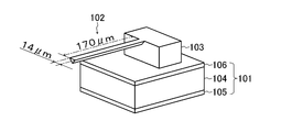
- FIG. 1 is a perspective view showing a configuration of a solid-state quantum memory according to an embodiment of the present invention.
- FIG. 2A is a characteristic diagram showing the resonance characteristics of the vibrating unit 102 in the secondary vibration mode.
- FIG. 2B is a distribution diagram showing the distribution of strain of the excited vibrating portion 102.
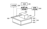
- FIG. 3 is a configuration diagram showing a configuration of a measurement system for measuring the state of energy control in the electron 2 level system by the rare earth element introduced into the vibrating unit 102.
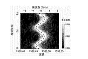
- FIG. 4 is a distribution diagram showing the measurement results of photoluminescence light from each bound exciton level of the electron 2 level system formed in the vibrating portion 102.
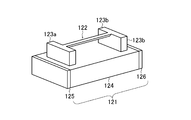
- FIG. 5 is a perspective view showing the configuration of another solid-state quantum memory according to the embodiment of the present invention.
- This solid-state quantum memory includes a vibrating unit 102 that is supported on the substrate 101 so as to be displaceable (vibrating), and an exciting unit that excites the vibrating unit 102.
- a rare earth element is introduced into the vibrating portion 102, and an electron two-level system composed of the introduced rare earth element is formed.
- Rare earth elements are introduced into the vibrating section 102 in the form of ions.
- the vibrating portion 102 is supported by the supporting portion 103 on the substrate 101.
- the vibrating portion 102 is a cantilever beam supported by the supporting portion 103.
- the support portion 103 and the vibrating portion 102 are integrally formed.
- the vibrating portion 102 is, for example, a triangular prism having an isosceles triangle shape on the bottom surface, and has a length of 170 ⁇ m, a width of 14 ⁇ m, and a thickness of 7 ⁇ m.
- the length of the base of the isosceles triangle on the bottom surface of the vibrating portion 102, which is a triangular prism, is 14 ⁇ m, and the height is 7 ⁇ m.
- the vibrating unit 102 can be composed of, for example, yttrium silicate (Y 2 SiO 5).
- the rare earth element can be, for example, erbium (Er). Er is an ion whose energy level has Kramers theorem. Rare earth elements are dispersed in the vibrating unit 102.
- the rare earth element can also be configured such that the clusters are dispersed in the vibrating portion 102.
- the vibrating portion 102 (support portion 103) can be formed by three-dimensionally processing the Y 2 SiO 5 material in which Er is introduced by a known focused ion beam (FIB).
- FIB focused ion beam
- the vibrating portion 102 having a columnar shape is laminated by laminating a layer of a material constituting the vibrating portion 102 and a layer of a rare earth element in the thickness direction, for example, by using a molecular beam epitaxial growth method or the like. It can also be a structure.
- the layer of the material constituting the vibrating portion 102 and the layer of the rare earth element can be alternately laminated to form the vibrating portion 102.
- the substrate 101 can be used as an excitation unit.
- the substrate 101 can be composed of a piezoelectric element 104 made of a piezoelectric material and a first electrode 105 and a second electrode 106 formed by sandwiching the piezoelectric element 104.
- an excitation signal electrical signal
- the vibrating portion 102 supported and fixed to the substrate 101 via the supporting portion 103 is provided.
- the excitation state of the vibrating unit 102 (dynamic distortion generated in the vibrating unit 102) can be controlled.
- FIGS. 2A and 2B the resonance characteristics of the vibrating unit 102 in the secondary vibration mode and the distribution of the strain of the vibrating unit 102 excited by the electric signal near 1.57 MHz will be described with reference to FIGS. 2A and 2B.
- FIG. 2A it can be seen that the resonance frequency of the vibrating unit 102 is around 1.57 MHz.
- FIG. 2B a large strain (dynamic strain) is generated in the vicinity of the central portion of the vibrating portion 102 of the beam structure due to the excitation of the exciting portion by the excitation signal of the resonance frequency. You can see that.
- the state of energy control of this electron level can be measured by photoluminescence excitation (photoluminescence) measurement.
- a measurement system for carrying out this measurement will be described with reference to FIG.
- This measurement system includes a light source 201, an acoustic optical element 202, a signal generator 203, and a spectroscope 204.
- a predetermined high-frequency signal is applied from the signal generator 203 to the electrodes of the substrate 101 serving as the excitation unit and the acoustic optical element 202.
- the vibrating unit 102 is vibrated to vibrate the vibrating unit 102, and the vibrating unit 102 is irradiated with continuous wave laser light having a wavelength of 1536 nm emitted from the light source 201 made of a laser in the form of a pulse by the acoustic optical element 202.
- the wavelength of 1536 nm is the optical transition wavelength of Er.
- Photoluminescence (PL) light is obtained from each bound exciton level of the electron two-level system (Er) formed in the vibrating portion 102 by irradiating the pulsed laser beam. This PL light is measured by the spectroscope 204.
- the bound exciter level in a state where various strains are applied by changing the relative phase between the pulse waveform of the laser beam irradiating the vibrating unit 102 and the vibration of the exciting vibrating unit 102. It becomes possible to measure the energy of.
- the measurement was carried out in an environment of extremely low temperature and high vacuum (4K, 1 ⁇ 10 -4 Pa or less) to confirm the principle.
- FIG. 4 The above-mentioned measurement result of PL light is shown in FIG. As shown in FIG. 4, it is shown that energy control of about ⁇ 2 GHz is performed by applying a high frequency signal having a voltage of 5 V. This value is sufficiently larger than the non-uniform spread of the electron level of general Er (about 1 GHz), suggesting that coherence can be improved even in a no-magnetic field environment. Since the magnetic field is not used in the holding control (memory control) of the quantum state at the electron level using the solid-state quantum memory according to the embodiment, when the magnetic field is used in the integration of the elements and the reduction of power consumption. Has an advantage in comparison. Further, according to the technique of the embodiment, it is also a feature that the coherence does not decrease due to the instability of the magnetic field.
- the solid-state quantum memory of the present invention may have a beam structure having both sides of the vibrating portion 122.
- This solid-state quantum memory includes a vibrating portion 122 that is supported on the substrate 121 so as to be displaceable (vibrating), and an exciting portion that excites the vibrating portion 122.
- a rare earth element is introduced into the vibrating portion 122, and an electron two-level system composed of the introduced rare earth element is formed.
- the vibrating portion 122 is supported on the substrate 121 by the first supporting portion 123a and the second supporting portion 123b.
- the vibrating portion 102 is a double-sided beam whose both ends are supported and fixed to the two first support portions 123a and the second support portion 123b.
- the vibrating portion 122 may have, for example, a triangular prism having an isosceles triangle shape on the bottom surface, and may have a length of 100 ⁇ m, a width of 20 ⁇ m, and a thickness of 10 ⁇ m.
- the length of the base of the isosceles triangle on the bottom surface of the vibrating portion 122, which is a triangular prism, is 20 ⁇ m, and the height is 10 ⁇ m.
- the vibrating portion 122 (first support portion 123a, second support portion 123b) is formed by three-dimensionally processing the Y 2 SiO 5 material in which Er is introduced by a known focused ion beam. can.
- the substrate 121 can be used as an excitation unit by forming the substrate 121 from a piezoelectric material.
- the substrate 121 can be composed of a piezoelectric element 124 made of a piezoelectric material and a first electrode 125 and a second electrode 126 formed by sandwiching the piezoelectric element 124.
- an excitation signal electric signal
- the substrate 121 is supported via the first support portion 123a and the second support portion 123b.
- the fixed vibrating portion 122 can be excited. Further, by controlling the excitation signal described above, it is possible to control the excitation state of the vibrating unit 122 (dynamic distortion generated in the vibrating unit 122).
- the vibrating portion is formed by using the piezoelectric element 124 that expands and contracts in the arrangement direction of the two first electrodes 125 and the second electrode 126, in other words, in the extending direction of the vibrating portion 122 having a double-sided beam structure.
- the tensile stress applied to 122 can be electrically controlled.
- an electric signal (voltage signal) of a predetermined frequency between the first electrode 125 and the second electrode 126 when the displacement at both ends of the vibrating portion 122 becomes 100 nm, a stress of about 10 MPa is applied to the vibrating portion 122. It is estimated from numerical calculations that it will occur. Since this stress causes an energy change of about 4 GHz, by using the vibrating portion 122 having a double-sided beam structure, the precision of the resonance energy of the electron two-level system composed of rare earth elements contained in the vibrating portion 122 is precise. Control is possible.
- Y 2 SiO 5 is used as the base material of the vibrating part, and Er is introduced therein, but the present invention is not limited to these.
- Er having resonance in the communication wavelength band has attracted the most attention, but neodymium (optical transition wavelength example: 1064 nm), ytterbium, etc. can also be used as rare earth elements. These also become ions whose energy level has Kramers theorem, and the same action and effect as when Er is used can be obtained.
- the measurement (emission excitation measurement) of the solid quantum memory according to the embodiment regarding the state of energy control of the electron level is performed in an extremely low temperature and high vacuum (4K, 1 ⁇ 10 -4 Pa or less) environment to confirm the principle.
- the operation of the solid-state quantum memory according to the present invention is not limited to a specific environment.
- the vibrating portion has a triangular prism beam structure, but the present invention is not limited to this, and various other mechanical drive mechanisms (flat plate type vibrator, surface acoustic wave, etc.) are similarly used. Can be used. Further, although an example in which a piezoelectric element is used as the strain applying means is shown, other strain applying means using electricity (electrostatic force), light (radiation pressure), heat (thermal expansion), etc. can also be used in the same manner. can.
- the electron two-level system is constructed from the rare earth elements introduced into the vibrating part, the entire system for realizing the quantum memory can be downsized and the power consumption can be reduced. can.
Landscapes
- Engineering & Computer Science (AREA)
- Physics & Mathematics (AREA)
- Theoretical Computer Science (AREA)
- General Physics & Mathematics (AREA)
- Data Mining & Analysis (AREA)
- Mathematical Physics (AREA)
- Evolutionary Computation (AREA)
- Computational Mathematics (AREA)
- Mathematical Analysis (AREA)
- Mathematical Optimization (AREA)
- Pure & Applied Mathematics (AREA)
- Computing Systems (AREA)
- General Engineering & Computer Science (AREA)
- Condensed Matter Physics & Semiconductors (AREA)
- Software Systems (AREA)
- Artificial Intelligence (AREA)
- Chemical & Material Sciences (AREA)
- Inorganic Chemistry (AREA)
- Manufacturing & Machinery (AREA)
- Semiconductor Memories (AREA)
- Micromachines (AREA)
Abstract
固体量子メモリは、基板(101)の上に変位(振動)可能に支持された振動部(102)と、振動部(102)を励振する励振部とを備える。振動部(102)には、希土類元素が導入され、導入されている希土類元素から構成された電子2準位系が形成されている。基板(101)の上に、支持部(103)によって振動部(102)が支持されている。圧電材料から構成された圧電素子(104)と、圧電素子(104)を挾んで形成された第1電極(105),第2電極(106)とから構成された基板(101)が励振部となる。
Description
本発明は、振動部に導入した電子2準位系によりメモリを構成する固体量子メモリに関する。
半導体や固体中の不純物によって形成される電子2準位系は、この光吸収・発光特性を利用することで、光の量子状態を電子の量子状態として保持することが可能である。特に、希土類元素のエルビウム(Er)を内包する固体材料は、通信波長帯に共鳴した電子準位を有しており、また、電子準位における量子状態の保持時間(コヒーレンス)が非常に長いことから、量子メモリとしての応用が期待されている(非特許文献1)。
ここで、Erは、エネルギー準位がクラマース縮退を持つイオンとなる。この種の元素は、無磁場においてエネルギー縮退した電子準位を有しており、長いコヒーレンスを得るためには、電子準位の不均一広がりを超える大きなエネルギー変化を与えることが必要である。
Erについては、これまでに、7Tの外部磁場を印加することで、電子-核スピン結合で現れる超微細構造において、1GHz以上のエネルギー制御が報告されており、Er中の電子スピンにおいて1秒以上の長いコヒーレンスが実現されていた(非特許文献2)。また、マイクロ波を用いた電子制御を行うために、外部磁場による電子準位のエネルギー制御が用いられていた(非特許文献3)。
E. Saglamyurek et al., "Quantum storage of entangled telecom-wavelength photons in an erbium-doped optical fibre", Nature Photonics, vol. 9, pp. 83-87, 2015.
M. Rancic et al., "Coherence time of over a second in a telecom-compatible quantum memory storage material", Nature Physics, vol. 14, pp. 50-54, 2018.
J. R. Everts et al., "Microwave to optical photon conversion via fully concentrated rare-earth-ion crystals", Physical Review A, vol. 99, no. 6, 063830, 2019.
上述したように、従来は、量子メモリ実現のため電子準位における量子状態の保持制御に、外部磁場を用いていた。この外部磁場を発生するためには、巨大な超電導コイルが必要となり、量子メモリを実現するためのシステム全体の小型化や低消費電力化が困難であった。
本発明は、以上のような問題点を解消するためになされたものであり、量子メモリを実現するためのシステム全体の小型化、低消費電力化を目的とする。
本発明に係る固体量子メモリは、基板の上に変位可能に支持された振動部と、振動部を励振する励振部と、振動部に導入されている希土類元素から構成された電子2準位系とを備える。
以上説明したように、本発明によれば、振動部に導入した希土類元素から電子2準位系を構成したので、量子メモリを実現するためのシステム全体の小型化、低消費電力化が実現できる。
以下、本発明の実施の形態に係る固体量子メモリについて図1を参照して説明する。この固体量子メモリは、基板101の上に変位(振動)可能に支持された振動部102と、振動部102を励振する励振部とを備える。振動部102には、希土類元素が導入され、導入されている希土類元素から構成された電子2準位系が形成されている。希土類元素は、振動部102にイオンの状態で導入されている。
この例では、基板101の上に、支持部103によって振動部102が支持されている。振動部102は、支持部103に支持された片持ちの梁である。この例では、支持部103と振動部102とは、一体に形成されている。振動部102は、例えば、底面の形状が2等辺三角形の三角柱であり、長さ170μm、幅14μm、厚さ7μmとされている。三角柱とされている振動部102の底面の2等辺三角形の底辺の長さが14μmであり、高さが7μmである。
振動部102は、例えば、イットリウムシリケイト(Y2SiO5)から構成することができる。希土類元素は、例えば、エルビウム(Er)とすることができる。Erは、エネルギー準位がクラマース縮退を持つイオンとなる。希土類元素は、振動部102に分散されている。また、希土類元素は、このクラスターが、振動部102に分散された構成することもできる。例えば、Erが導入されているY2SiO5材料を、公知の収束イオンビーム(FIB)により立体加工することで、振動部102(支持部103)が形成できる。
また、柱状とされている振動部102は、例えば、分子線エピタキシャル成長法などを用いることで、この厚さ方向に、振動部102を構成する材料の層と、希土類元素の層とを積層した積層構造とすることもできる。例えば、振動部102を構成する材料の層と、希土類元素の層とを交互に積層して振動部102とすることができる。
例えば、基板101を圧電材料から構成することで、基板101を励振部とすることができる。例えば、圧電材料から構成された圧電素子104と、圧電素子104を挾んで形成された第1電極105,第2電極106とから基板101を構成することができる。第1電極105と第2電極106との間に励振信号(電気信号)を印加し、圧電素子104を振動させることで、基板101に支持部103を介して支持固定されている振動部102を励振することができる。また、上述した励振信号の制御により、振動部102の励振状態(振動部102に発生する動的な歪)を制御することができる。
次に、振動部102の2次の振動モードにおける共振特性と、1.57MHz付近の電気信号により励振した振動部102の歪の分布について、図2A、図2Bを参照して説明する。まず、図2Aに示すように、振動部102の共振周波数は、1.57MHz付近であることがわかる。また、共振周波数の励振信号による励振部の励振で、図2Bの動的歪分布に示すように、梁構造の振動部102の中央部近傍に、大きな歪(動的歪)が発生していることがわかる。
次に、振動部102に加わる歪による、振動部102に導入された希土類元素の電子準位のエネルギー制御について説明する。この電子準位のエネルギー制御の状態は、発光励起(Photo luminescence excitatio)測定により測定できる。この測定を実施する測定系について、図3を参照して説明する。この測定系は、光源201,音響光学素子202,信号生成器203,分光器204を備える。まず、信号生成器203から、励振部となる基板101の電極および音響光学素子202に所定の高周波信号を印加する。
これにより、励振部を振動させて振動部102を励振した状態で、レーザからなる光源201より出射する波長1536nmの連続波レーザ光を、音響光学素子202によりパルス状として振動部102に照射する。波長1536nmは、Erの光学遷移波長である。パルス状のレーザ光照射により、振動部102に形成されている電子2準位系(Er)の、各束縛励起子準位からフォトルミネッセンス(PL)光が得られる。このPL光を分光器204で測定する。この測定において、振動部102に照射するレーザ光のパルス波形と、励振している振動部102の振動と間の相対位相を変化させることで、様々な歪を印加した状態における束縛励起子準位のエネルギーを測ることが可能になる。なお、測定は、原理確認のため極低温高真空(4K,1×10-4Pa以下)の環境下において実施した。
上述したPL光の測定結果を図4に示す。図4に示すように、電圧が5Vの高周波信号の印加により、±2GHz程度のエネルギー制御が行われていることを示している。この値は、一般的なErの電子準位の不均一広がり(1GHz程度)よりも十分大きく、無磁場環境下においても、コヒーレンスの向上が可能であることを示唆している。実施の形態に係る固体量子メモリを用いた、電子準位における量子状態の保持制御(記憶制御)では、磁場を用いないことから、素子の集積化、低消費電力化において、磁場を用いる場合に比較して優位性を有する。また、実施の形態の技術によれば、磁場の不安定性によるコヒーレンスの減少が起きないことも特徴である。
ところで、本発明の固体量子メモリは、図5に示すように、振動部122を両持ちの梁構造とすることもできる。この固体量子メモリは、基板121の上に変位(振動)可能に支持された振動部122と、振動部122を励振する励振部とを備える。振動部122には、希土類元素が導入され、導入されている希土類元素から構成された電子2準位系が形成されている。
この例では、基板121の上に、第1支持部123aと第2支持部123bとによって振動部122が支持されている。振動部102は、2つの第1支持部123a、第2支持部123bに両端が支持固定された両持ちの梁である。振動部122は、例えば、底面の形状が2等辺三角形の三角柱とすることができ、長さ100μm、幅20μm、厚さ10μmとすることができる。三角柱とされている振動部122の底面の2等辺三角形の底辺の長さが20μmであり、高さが10μmである。この場合においても、例えば、Erが導入されているY2SiO5材料を、公知の収束イオンビームにより立体加工することで、振動部122(第1支持部123a、第2支持部123b)が形成できる。
また、この例においても、基板121を圧電材料から構成することで、基板121を励振部とすることができる。例えば、圧電材料から構成された圧電素子124と、圧電素子124を挾んで形成された第1電極125,第2電極126とから基板121を構成することができる。第1電極125と第2電極126との間に励振信号(電気信号)を印加し、圧電素子124を振動させることで、基板121に第1支持部123a、第2支持部123bを介して支持固定されている振動部122を励振することができる。また、上述した励振信号の制御により、振動部122の励振状態(振動部122に発生する動的な歪)を制御することができる。
この構造では、2つの第1電極125、第2電極126の配置方向、言い換えると、両持ち梁構造とされている振動部122の延在方向に伸縮する圧電素子124を用いることで、振動部122に加わる引張応力を電気的に制御可能となる。所定の周波数の電気信号(電圧信号)を第1電極125と第2電極126との間に印加することで、振動部122の両端の変位が100nmとなると、振動部122に10MPa程度の応力が発生することが数値計算から見積もられる。この応力は、4GHz程度のエネルギー変化を生むため、両持ちの梁構造とした振動部122を用いることで、振動部122に含まれる希土類元素から構成された電子2準位系の共鳴エネルギーの精密制御が可能となる。
なお、上述では、振動部の母材としてY2SiO5を用い、これにErを導入したが、これらの限るものではない。固体量子メモリとしては、例えば、通信波長帯に共鳴を有するErが最も注目を集めているが、希土類元素として、ネオジウム(光学遷移波長例:1064nm)やイッテルビウムなども用いることができる。これらも、エネルギー準位がクラマース縮退を持つイオンとなり、Erを用いた場合と同様の作用効果が得られる。
また、実施の形態に係る固体量子メモリの、電子準位のエネルギー制御の状態に関する測定(発光励起測定)は、原理確認のため極低温高真空(4K,1×10-4Pa以下)環境下において実施したが、本発明に係る固体量子メモリの動作は、特定の環境下に限られるものではない。
また、上述した実施の形態では、振動部を、三角柱の梁構造としたが、これに限るものではなく、他の様々な機械的駆動機構(平板型振動子、表面弾性波など)を同様に用いることができる。また、歪の印加手段として圧電素子を用いた例を示したが、他の電気(静電力)、光(放射圧)、熱(熱膨張)などを用いた歪印加手段も同様に用いることができる。
以上に説明したように、本発明によれば、振動部に導入した希土類元素から電子2準位系を構成したので、量子メモリを実現するためのシステム全体の小型化、低消費電力化が実現できる。
なお、本発明は以上に説明した実施の形態に限定されるものではなく、本発明の技術的思想内で、当分野において通常の知識を有する者により、多くの変形および組み合わせが実施可能であることは明白である。
101…基板、102…振動部、103…支持部、104…圧電素子、105…第1電極、106…第2電極。
Claims (6)
- 基板の上に変位可能に支持された振動部と、
前記振動部を励振する励振部と、
前記振動部に導入されている希土類元素から構成された電子2準位系と
を備える固体量子メモリ。 - 請求項1記載の固体量子メモリにおいて、
前記希土類元素は、前記振動部にイオンの状態で導入されていることを特徴とする固体量子メモリ。 - 請求項1または2記載の固体量子メモリにおいて、
前記希土類元素は、イオンのエネルギー準位がクラマース縮退を持つことを特徴とする固体量子メモリ。 - 請求項1~3のいずれか1項に記載の固体量子メモリにおいて、
前記振動部は、片持ち梁構造とされていることを特徴とする固体量子メモリ。 - 請求項1~3のいずれか1項に記載の固体量子メモリにおいて、
前記振動部は、両持ち梁構造とされていることを特徴とする固体量子メモリ。 - 請求項1~5のいずれか1項に記載の固体量子メモリにおいて、
前記励振部は、圧電材料から構成されていることを特徴とする固体量子メモリ。
Priority Applications (3)
| Application Number | Priority Date | Filing Date | Title |
|---|---|---|---|
| PCT/JP2020/009939 WO2021181444A1 (ja) | 2020-03-09 | 2020-03-09 | 固体量子メモリ |
| US17/799,560 US20230054881A1 (en) | 2020-03-09 | 2020-03-09 | Solid-State Quantum Memory |
| JP2022506991A JP7351404B2 (ja) | 2020-03-09 | 2020-03-09 | 固体量子メモリ |
Applications Claiming Priority (1)
| Application Number | Priority Date | Filing Date | Title |
|---|---|---|---|
| PCT/JP2020/009939 WO2021181444A1 (ja) | 2020-03-09 | 2020-03-09 | 固体量子メモリ |
Publications (1)
| Publication Number | Publication Date |
|---|---|
| WO2021181444A1 true WO2021181444A1 (ja) | 2021-09-16 |
Family
ID=77670483
Family Applications (1)
| Application Number | Title | Priority Date | Filing Date |
|---|---|---|---|
| PCT/JP2020/009939 Ceased WO2021181444A1 (ja) | 2020-03-09 | 2020-03-09 | 固体量子メモリ |
Country Status (3)
| Country | Link |
|---|---|
| US (1) | US20230054881A1 (ja) |
| JP (1) | JP7351404B2 (ja) |
| WO (1) | WO2021181444A1 (ja) |
Citations (3)
| Publication number | Priority date | Publication date | Assignee | Title |
|---|---|---|---|---|
| WO2011036814A1 (ja) * | 2009-09-28 | 2011-03-31 | 株式会社 東芝 | 量子計算機および量子メモリー |
| JP2017151248A (ja) * | 2016-02-24 | 2017-08-31 | 日本電信電話株式会社 | 量子光学材料 |
| JP2019029511A (ja) * | 2017-07-31 | 2019-02-21 | 日本電信電話株式会社 | 固体量子メモリ |
Family Cites Families (2)
| Publication number | Priority date | Publication date | Assignee | Title |
|---|---|---|---|---|
| JP6030591B2 (ja) | 2014-03-04 | 2016-11-24 | 日本電信電話株式会社 | 量子メモリの制御方法 |
| US11696507B2 (en) * | 2018-12-14 | 2023-07-04 | Stmicroelectronics S.R.L. | Piezoelectric MEMS device with a suspended membrane having high mechanical shock resistance and manufacturing process thereof |
-
2020
- 2020-03-09 US US17/799,560 patent/US20230054881A1/en active Pending
- 2020-03-09 WO PCT/JP2020/009939 patent/WO2021181444A1/ja not_active Ceased
- 2020-03-09 JP JP2022506991A patent/JP7351404B2/ja active Active
Patent Citations (3)
| Publication number | Priority date | Publication date | Assignee | Title |
|---|---|---|---|---|
| WO2011036814A1 (ja) * | 2009-09-28 | 2011-03-31 | 株式会社 東芝 | 量子計算機および量子メモリー |
| JP2017151248A (ja) * | 2016-02-24 | 2017-08-31 | 日本電信電話株式会社 | 量子光学材料 |
| JP2019029511A (ja) * | 2017-07-31 | 2019-02-21 | 日本電信電話株式会社 | 固体量子メモリ |
Also Published As
| Publication number | Publication date |
|---|---|
| JPWO2021181444A1 (ja) | 2021-09-16 |
| US20230054881A1 (en) | 2023-02-23 |
| JP7351404B2 (ja) | 2023-09-27 |
Similar Documents
| Publication | Publication Date | Title |
|---|---|---|
| Annapureddy et al. | Enhanced magnetic energy harvesting properties of magneto-mechano-electric generator by tailored geometry | |
| JP2015524166A (ja) | マイクロ波または高周波の誘導放出を発生させるためのデバイスおよび方法 | |
| JPH11300274A (ja) | 圧力波発生装置 | |
| TW200916876A (en) | RF phase modulation technique for performing acousto-optic intensity modulation of an optical wavefront | |
| US8633472B2 (en) | Tunable terahertz radiation source | |
| Song et al. | Self-powered light dimming system using a magneto-mechano-electric generator with hardener-doped Pb (Mg 1/3 Nb 2/3) O 3–Pb (Zr, Ti) O 3 single crystals | |
| Yoder et al. | Side-coupled slab-symmetric structure for high-gradient acceleration using terahertz power | |
| Nakamura et al. | Piezoelectric transformers using LiNbO3 single crystals | |
| JP7351404B2 (ja) | 固体量子メモリ | |
| RU2742569C1 (ru) | Осциллятор для генератора терагерцового излучения | |
| US3354407A (en) | Piezo-electric modulation of lasers | |
| US6067308A (en) | Electroluminescent solid state device | |
| KR102454903B1 (ko) | 압전 복합체, 그 제조방법, 및 이를 포함하는 자기전기 적층형 구조체 | |
| CN107403616A (zh) | 一种低频框架驱动式四边型弯张换能器 | |
| Laoratanakul et al. | Designing a radial mode laminated piezoelectric transformer for high power applications | |
| Sessler et al. | Tensile and bending piezoelectricity of single-film PVDF monomorphs and bimorphs | |
| JP6813453B2 (ja) | 固体量子メモリ | |
| EP0762565A2 (en) | Solid state device for generating electromagnetic wave in terahertz-band | |
| CN110932671B (zh) | 微梁长度调谐的超谐波共振信号频率放大装置 | |
| CN119315254B (zh) | 一种多场驱动正反馈的甚低频磁电天线阵列 | |
| CN119315253B (zh) | 具有非易失重构频带和方向图的甚低频多铁机械天线 | |
| CN120220639B (zh) | 一种多点驱动幅相控制弯曲板低频换能器 | |
| Yashvanth et al. | A new scheme for high frequency ultrasound generation | |
| CN116840529B (zh) | 一种多频段低频磁信号发生器 | |
| KR101011679B1 (ko) | 공동 공진기 한쪽 면을 이용한 펄스 전자 증폭기 |
Legal Events
| Date | Code | Title | Description |
|---|---|---|---|
| 121 | Ep: the epo has been informed by wipo that ep was designated in this application |
Ref document number: 20924671 Country of ref document: EP Kind code of ref document: A1 |
|
| ENP | Entry into the national phase |
Ref document number: 2022506991 Country of ref document: JP Kind code of ref document: A |
|
| NENP | Non-entry into the national phase |
Ref country code: DE |
|
| 122 | Ep: pct application non-entry in european phase |
Ref document number: 20924671 Country of ref document: EP Kind code of ref document: A1 |