WO2021172014A1 - 照明装置及び表示装置 - Google Patents
照明装置及び表示装置 Download PDFInfo
- Publication number
- WO2021172014A1 WO2021172014A1 PCT/JP2021/004902 JP2021004902W WO2021172014A1 WO 2021172014 A1 WO2021172014 A1 WO 2021172014A1 JP 2021004902 W JP2021004902 W JP 2021004902W WO 2021172014 A1 WO2021172014 A1 WO 2021172014A1
- Authority
- WO
- WIPO (PCT)
- Prior art keywords
- light
- light emitting
- layer
- lighting device
- emitting elements
- Prior art date
- Legal status (The legal status is an assumption and is not a legal conclusion. Google has not performed a legal analysis and makes no representation as to the accuracy of the status listed.)
- Ceased
Links
Images


Classifications
-
- G—PHYSICS
- G02—OPTICS
- G02F—OPTICAL DEVICES OR ARRANGEMENTS FOR THE CONTROL OF LIGHT BY MODIFICATION OF THE OPTICAL PROPERTIES OF THE MEDIA OF THE ELEMENTS INVOLVED THEREIN; NON-LINEAR OPTICS; FREQUENCY-CHANGING OF LIGHT; OPTICAL LOGIC ELEMENTS; OPTICAL ANALOGUE/DIGITAL CONVERTERS
- G02F1/00—Devices or arrangements for the control of the intensity, colour, phase, polarisation or direction of light arriving from an independent light source, e.g. switching, gating or modulating; Non-linear optics
- G02F1/01—Devices or arrangements for the control of the intensity, colour, phase, polarisation or direction of light arriving from an independent light source, e.g. switching, gating or modulating; Non-linear optics for the control of the intensity, phase, polarisation or colour
- G02F1/13—Devices or arrangements for the control of the intensity, colour, phase, polarisation or direction of light arriving from an independent light source, e.g. switching, gating or modulating; Non-linear optics for the control of the intensity, phase, polarisation or colour based on liquid crystals, e.g. single liquid crystal display cells
- G02F1/133—Constructional arrangements; Operation of liquid crystal cells; Circuit arrangements
- G02F1/1333—Constructional arrangements; Manufacturing methods
- G02F1/1335—Structural association of cells with optical devices, e.g. polarisers or reflectors
- G02F1/1336—Illuminating devices
- G02F1/133602—Direct backlight
-
- G—PHYSICS
- G02—OPTICS
- G02F—OPTICAL DEVICES OR ARRANGEMENTS FOR THE CONTROL OF LIGHT BY MODIFICATION OF THE OPTICAL PROPERTIES OF THE MEDIA OF THE ELEMENTS INVOLVED THEREIN; NON-LINEAR OPTICS; FREQUENCY-CHANGING OF LIGHT; OPTICAL LOGIC ELEMENTS; OPTICAL ANALOGUE/DIGITAL CONVERTERS
- G02F1/00—Devices or arrangements for the control of the intensity, colour, phase, polarisation or direction of light arriving from an independent light source, e.g. switching, gating or modulating; Non-linear optics
- G02F1/01—Devices or arrangements for the control of the intensity, colour, phase, polarisation or direction of light arriving from an independent light source, e.g. switching, gating or modulating; Non-linear optics for the control of the intensity, phase, polarisation or colour
- G02F1/13—Devices or arrangements for the control of the intensity, colour, phase, polarisation or direction of light arriving from an independent light source, e.g. switching, gating or modulating; Non-linear optics for the control of the intensity, phase, polarisation or colour based on liquid crystals, e.g. single liquid crystal display cells
- G02F1/133—Constructional arrangements; Operation of liquid crystal cells; Circuit arrangements
- G02F1/1333—Constructional arrangements; Manufacturing methods
- G02F1/1335—Structural association of cells with optical devices, e.g. polarisers or reflectors
- G02F1/1336—Illuminating devices
- G02F1/133602—Direct backlight
- G02F1/133603—Direct backlight with LEDs
-
- F—MECHANICAL ENGINEERING; LIGHTING; HEATING; WEAPONS; BLASTING
- F21—LIGHTING
- F21S—NON-PORTABLE LIGHTING DEVICES; SYSTEMS THEREOF; VEHICLE LIGHTING DEVICES SPECIALLY ADAPTED FOR VEHICLE EXTERIORS
- F21S2/00—Systems of lighting devices, not provided for in main groups F21S4/00 - F21S10/00 or F21S19/00, e.g. of modular construction
-
- G—PHYSICS
- G02—OPTICS
- G02F—OPTICAL DEVICES OR ARRANGEMENTS FOR THE CONTROL OF LIGHT BY MODIFICATION OF THE OPTICAL PROPERTIES OF THE MEDIA OF THE ELEMENTS INVOLVED THEREIN; NON-LINEAR OPTICS; FREQUENCY-CHANGING OF LIGHT; OPTICAL LOGIC ELEMENTS; OPTICAL ANALOGUE/DIGITAL CONVERTERS
- G02F1/00—Devices or arrangements for the control of the intensity, colour, phase, polarisation or direction of light arriving from an independent light source, e.g. switching, gating or modulating; Non-linear optics
- G02F1/01—Devices or arrangements for the control of the intensity, colour, phase, polarisation or direction of light arriving from an independent light source, e.g. switching, gating or modulating; Non-linear optics for the control of the intensity, phase, polarisation or colour
- G02F1/13—Devices or arrangements for the control of the intensity, colour, phase, polarisation or direction of light arriving from an independent light source, e.g. switching, gating or modulating; Non-linear optics for the control of the intensity, phase, polarisation or colour based on liquid crystals, e.g. single liquid crystal display cells
- G02F1/133—Constructional arrangements; Operation of liquid crystal cells; Circuit arrangements
- G02F1/1333—Constructional arrangements; Manufacturing methods
- G02F1/1335—Structural association of cells with optical devices, e.g. polarisers or reflectors
- G02F1/1336—Illuminating devices
- G02F1/133602—Direct backlight
- G02F1/133606—Direct backlight including a specially adapted diffusing, scattering or light controlling members
- G02F1/133607—Direct backlight including a specially adapted diffusing, scattering or light controlling members the light controlling member including light directing or refracting elements, e.g. prisms or lenses
-
- G—PHYSICS
- G02—OPTICS
- G02F—OPTICAL DEVICES OR ARRANGEMENTS FOR THE CONTROL OF LIGHT BY MODIFICATION OF THE OPTICAL PROPERTIES OF THE MEDIA OF THE ELEMENTS INVOLVED THEREIN; NON-LINEAR OPTICS; FREQUENCY-CHANGING OF LIGHT; OPTICAL LOGIC ELEMENTS; OPTICAL ANALOGUE/DIGITAL CONVERTERS
- G02F1/00—Devices or arrangements for the control of the intensity, colour, phase, polarisation or direction of light arriving from an independent light source, e.g. switching, gating or modulating; Non-linear optics
- G02F1/01—Devices or arrangements for the control of the intensity, colour, phase, polarisation or direction of light arriving from an independent light source, e.g. switching, gating or modulating; Non-linear optics for the control of the intensity, phase, polarisation or colour
- G02F1/13—Devices or arrangements for the control of the intensity, colour, phase, polarisation or direction of light arriving from an independent light source, e.g. switching, gating or modulating; Non-linear optics for the control of the intensity, phase, polarisation or colour based on liquid crystals, e.g. single liquid crystal display cells
- G02F1/133—Constructional arrangements; Operation of liquid crystal cells; Circuit arrangements
- G02F1/1333—Constructional arrangements; Manufacturing methods
- G02F1/1335—Structural association of cells with optical devices, e.g. polarisers or reflectors
- G02F1/1336—Illuminating devices
- G02F1/133614—Illuminating devices using photoluminescence, e.g. phosphors illuminated by UV or blue light
-
- F—MECHANICAL ENGINEERING; LIGHTING; HEATING; WEAPONS; BLASTING
- F21—LIGHTING
- F21Y—INDEXING SCHEME ASSOCIATED WITH SUBCLASSES F21K, F21L, F21S and F21V, RELATING TO THE FORM OR THE KIND OF THE LIGHT SOURCES OR OF THE COLOUR OF THE LIGHT EMITTED
- F21Y2105/00—Planar light sources
- F21Y2105/10—Planar light sources comprising a two-dimensional [2D] array of point-like light-generating elements
- F21Y2105/14—Planar light sources comprising a two-dimensional [2D] array of point-like light-generating elements characterised by the overall shape of the two-dimensional [2D] array
- F21Y2105/16—Planar light sources comprising a two-dimensional [2D] array of point-like light-generating elements characterised by the overall shape of the two-dimensional [2D] array square or rectangular, e.g. for light panels
-
- F—MECHANICAL ENGINEERING; LIGHTING; HEATING; WEAPONS; BLASTING
- F21—LIGHTING
- F21Y—INDEXING SCHEME ASSOCIATED WITH SUBCLASSES F21K, F21L, F21S and F21V, RELATING TO THE FORM OR THE KIND OF THE LIGHT SOURCES OR OF THE COLOUR OF THE LIGHT EMITTED
- F21Y2115/00—Light-generating elements of semiconductor light sources
- F21Y2115/10—Light-emitting diodes [LED]
-
- G—PHYSICS
- G02—OPTICS
- G02F—OPTICAL DEVICES OR ARRANGEMENTS FOR THE CONTROL OF LIGHT BY MODIFICATION OF THE OPTICAL PROPERTIES OF THE MEDIA OF THE ELEMENTS INVOLVED THEREIN; NON-LINEAR OPTICS; FREQUENCY-CHANGING OF LIGHT; OPTICAL LOGIC ELEMENTS; OPTICAL ANALOGUE/DIGITAL CONVERTERS
- G02F1/00—Devices or arrangements for the control of the intensity, colour, phase, polarisation or direction of light arriving from an independent light source, e.g. switching, gating or modulating; Non-linear optics
- G02F1/01—Devices or arrangements for the control of the intensity, colour, phase, polarisation or direction of light arriving from an independent light source, e.g. switching, gating or modulating; Non-linear optics for the control of the intensity, phase, polarisation or colour
- G02F1/13—Devices or arrangements for the control of the intensity, colour, phase, polarisation or direction of light arriving from an independent light source, e.g. switching, gating or modulating; Non-linear optics for the control of the intensity, phase, polarisation or colour based on liquid crystals, e.g. single liquid crystal display cells
- G02F1/133—Constructional arrangements; Operation of liquid crystal cells; Circuit arrangements
- G02F1/1333—Constructional arrangements; Manufacturing methods
- G02F1/1335—Structural association of cells with optical devices, e.g. polarisers or reflectors
- G02F1/1336—Illuminating devices
- G02F1/133602—Direct backlight
- G02F1/133606—Direct backlight including a specially adapted diffusing, scattering or light controlling members
-
- G—PHYSICS
- G02—OPTICS
- G02F—OPTICAL DEVICES OR ARRANGEMENTS FOR THE CONTROL OF LIGHT BY MODIFICATION OF THE OPTICAL PROPERTIES OF THE MEDIA OF THE ELEMENTS INVOLVED THEREIN; NON-LINEAR OPTICS; FREQUENCY-CHANGING OF LIGHT; OPTICAL LOGIC ELEMENTS; OPTICAL ANALOGUE/DIGITAL CONVERTERS
- G02F2202/00—Materials and properties
- G02F2202/36—Micro- or nanomaterials
Definitions
- the embodiment of the present invention relates to a lighting device and a display device.
- a liquid crystal display device using a liquid crystal panel for display has been known as a display device mounted on a television, an information device, or the like. Due to the display quality of such a liquid crystal display device, there is an increasing demand for higher brightness of the lighting device used in the liquid crystal display device, and a direct type lighting in which a light source is arranged directly under the liquid crystal panel with a light guide plate in between. The device is under consideration.
- the present embodiment provides a lighting device having improved lighting quality and a display device provided with the lighting device.
- the lighting device includes a wiring substrate, a plurality of light emitting elements arranged on the main surface of the wiring substrate, a light diffusion distance maintaining layer provided on the plurality of light emitting elements, and the light diffusion.
- a wavelength conversion layer provided on the distance maintenance layer and a prism sheet provided on the wavelength conversion layer are provided, and the main surface of the wiring substrate is divided into a plurality of segment regions, and the plurality of segment regions are divided into a plurality of segment regions.
- Each of the n (n> 1) light emitting elements is provided, the plurality of light emitting elements are independently driven in the segment region unit, and the thicknesses of the light diffusion distance maintaining layers are adjacent to each other. It is 1 ⁇ 2 or more of the pitch of the segment region.
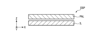
- FIG. 1 is a block diagram showing a display device DSP according to the present embodiment.
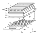
- FIG. 2 is an exploded perspective view showing the lighting device IL shown in FIG.
- FIG. 3 is a plan view showing a part of the lighting device IL according to the present embodiment.
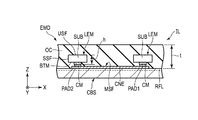
- FIG. 4 is a cross-sectional view showing the lighting device IL along the line AA of FIG.
- FIG. 5 is a cross-sectional view showing a light emitting element LEM along the line BB of FIG.
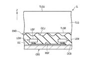
- FIG. 6 is a cross-sectional view showing another configuration example of the protective layer OC.
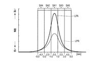
- FIG. 7 is a diagram showing the brightness profiles of the lighting device IL of this embodiment and the lighting device of the comparative example.
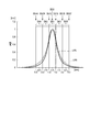
- FIG. 8 is a diagram showing brightness profiles in the present embodiment and the comparative example.
- first direction X, the second direction Y, and the third direction Z are orthogonal to each other, but may intersect at an angle other than 90 degrees.
- the direction toward the tip of the arrow in the third direction Z is defined as up or up, and the direction opposite to the direction toward the tip of the arrow in the third direction Z is defined as down or down.
- the second member in the case of "the second member above the first member” and “the second member below the first member”, the second member may be in contact with the first member or separated from the first member. May be located. In the latter case, a third member may be interposed between the first member and the second member. On the other hand, in the case of “the second member above the first member” and “the second member below the first member”, the second member is in contact with the first member.
- FIG. 1 is a block diagram showing a display device DSP according to the present embodiment.
- the display device DSP includes a display panel PNL and a lighting device IL.
- the display panel PNL is a generally known transmissive or transflective liquid crystal display panel.
- the display panel PNL is not limited to the liquid crystal display panel, and may be any display panel that requires a separate light source, such as a MEMS (Micro Electro-Mechanical System) display panel.
- MEMS Micro Electro-Mechanical System
- the lighting device IL is arranged facing below the display panel PNL.
- the illuminator IL emits light toward the display panel PNL.
- the lighting device IL functions as a backlight unit.
- the display panel PNL displays an image by selectively transmitting light from the illuminating device IL.
- FIG. 2 is an exploded perspective view showing the lighting device IL shown in FIG.
- FIG. 3 is a plan view showing a part of the lighting device IL according to the present embodiment.
- the illumination device IL includes a wiring board CBS, a plurality of light emitting elements LEM, a drive unit DVM, a protective layer OC, a light diffusion distance maintaining layer TLG, a wavelength conversion layer RCL, and a prism sheet. It is equipped with PSM.
- the wiring board CBS, the plurality of light emitting elements LEM, the protective layer OC, the light diffusion distance maintaining layer TLG, the wavelength conversion layer RCL, and the prism sheet PSM are laminated in this order in the third direction Z.
- the wiring board CBS is composed of a printed circuit board (PCB: Printed Circuit Board).
- PCB printed Circuit Board
- the wiring board CBS is not limited to a printed circuit board, and may be composed of a flexible printed circuit board (FPC).
- the wiring board CBS has a main surface MSF and has a light emitting region LA on the main surface MSF.
- the light emitting region LA faces at least the display region of the display panel (PNL).
- the plurality of light emitting elements LEM are mounted on the main surface MSF of the wiring board CBS.
- the light emitting element LEM is a mini LED (mini light emitting diode).
- a drive unit DVM that drives a plurality of light emitting elements LEM is mounted outside the light emission region LA.
- the light emitting element LEM outputs light having a specific wavelength, and the wavelength conversion layer RCL converts the wavelength of the light emitted from the light emitting element LEM and outputs it.
- the light emitting element LEM has a square shape.
- the shape of the light emitting element LEM may have a shape other than a square such as a rectangle.
- the length of one side of the light emitting element LEM, which is a mini LED is, for example, more than 100 ⁇ m and less than 300 ⁇ m.
- the length of one side of the light emitting element LEM, which is a mini LED may exceed 100 ⁇ m and may be 200 ⁇ m or less.
- the light emitting element LEM may be a micro LED having the longest side length of 100 ⁇ m or less as an LED having a size smaller than that of the mini LED.
- the light emitting element LEM may be an LED having the longest side length of 1 mm or less.
- the light emitting element LEM may be an LED having a longest side length of 1000 ⁇ m or more as a general LED having a size larger than that of the mini LED.
- the length of one side of the light emitting element LEM, which is the general LED, is, for example, 300 ⁇ m or more and 350 ⁇ m or less.
- the protective layer OC is configured as a light transmitting layer that transmits the wavelength of the light emitted by the light emitting element LEM.
- the protective layer OC is made of, for example, a silicon resin.
- the protective layer OC transmits the above light without converting the wavelength of the light emitted by the light emitting element LEM into another wavelength.
- the wavelength of the light transmitted through the protective layer OC is converted to another wavelength by the wavelength conversion layer RCL described later.
- the light diffusion distance maintaining layer TLG is located above the plurality of light emitting elements LEM with the protective layer OC interposed therebetween.
- the light diffusion distance maintaining layer TLG is a transparent resin layer made of a material having one kind of refractive index.
- the light diffusion distance maintaining layer TLG is a transparent resin layer composed of one kind of resin material, and more specifically, a plate-shaped polycarbonate resin.
- the space between the protective layer OC and the wavelength conversion layer RCL is maintained at a constant interval.
- the mini LED which is a light emitting element LEM, emits light having high directivity. Therefore, when the turns on the plurality of light emitting elements LEM, there is a risk that the user will be viewing these light-emitting elements LEM as a bright point dot pattern. In order to prevent the bright spots formed by the light emitting element LEM from being visually recognized, it is necessary to diffuse the highly directional emitted light from the light emitting element LED to such an extent that it cannot be visually recognized.
- the light diffusion distance maintaining layer TLG of the present embodiment has a sufficient thickness (distance in the third direction Z) necessary for the light emitted from the light emitting element LEM to diffuse in the third direction Z. Therefore, in the present embodiment, the occurrence of undesired light unevenness including the bright spot is suppressed.
- the light diffusion distance maintaining layer TLG is located between the light emitting element LEM and the display panel PNL. As a result, the light emitted from the light emitting element LEM is diffused toward the display panel PNL in the process of passing through the light diffusion distance maintaining layer TLG, and is mixed with the light from the adjacent light emitting element LEM.
- the brightness of the light after passing through the light diffusion distance maintaining layer TLG is made uniform over the entire emission surface (the entire emission surface corresponding to the light emission region LA). Therefore, the deterioration of the lighting quality of the lighting device IL can be suppressed, and the lighting quality is improved.
- the pitch of the segment region SA in the first direction X and the second direction Y is the pitch P and the thickness of the light diffusion distance maintaining layer TLG (the length in the third direction) is the thickness T. It is desirable that the thickness T is 1 ⁇ 2 or more of the pitch P. That is, T ⁇ (1/2) ⁇ P holds.
- the wavelength conversion layer RCL as a wavelength conversion element is located above the light diffusion distance maintenance layer TLG.
- the wavelength conversion layer RCL contains, for example, quantum dots as a light emitting material, absorbs incident light such as light emitted by the light emitting element LEM, and can emit light having a wavelength longer than the wavelength of the absorbed light. ..
- the light emitting element LEM is a blue LED having a main emission peak wavelength of 500 nm or less
- the wavelength conversion layer RCL is a phosphor that absorbs the light emitted from the light emitting element LEM and emits light having a wavelength of 500 nm or more.
- the wavelength conversion layer RCL is arranged on the light diffusion distance maintenance layer TLG, not between the light emitting element ELM and the light diffusion distance maintenance layer TLG.
- the wavelength conversion layer RCL is preferably arranged after the light diffusion distance maintaining layer TLG on the optical path of the light emitted by the light emitting element LEM.
- the wavelength conversion layer RCL is arranged between the light emitting element ELM and the light diffusion distance maintaining layer TLG.
- the light emitted from the light emitting element LEM is diffused by passing through the wavelength conversion layer RCL in the vicinity of the light emitting element LEM, and then is incident on the light diffusion distance maintaining layer TLG and is naturally diffused. Therefore, it is difficult for the emitted light from the light emitting element LEM to sufficiently reach the portion of the wavelength conversion layer RCL that is relatively far from the light emitting element LEM in a plan view, and the light diffusivity in the portion cannot be fully utilized. As a result, the diffusivity may be inferior.
- the light from the light emitting element ELM when the light from the light emitting element ELM first enters the light diffusion distance maintaining layer TLG, the light from the light emitting element ELM naturally diffuses radially in the process of passing through the light diffusion distance maintaining layer TLG, and then the wavelength conversion layer RCL. Further spread by.
- the emitted light from the light emitting element LEM sufficiently enters the wavelength conversion layer RCL even at a position away from the light emitting element LEM in a plan view, and is further diffused by the wavelength conversion layer RCL there.
- the diffusibility is improved in such a configuration. Therefore, it is preferable that the light diffusion distance maintaining layer TLG is closer to the light emitting element ELM than the wavelength conversion layer RCL.
- the prism sheet PSM is located above the wavelength conversion layer RCL.
- the prism sheet PSM is composed of two refractive prism sheets PSM1 and PSM2 arranged orthogonally.
- the prism sheet PSM may be composed of a total reflection type prism sheet instead of the refraction type prism sheet PSM1.
- the total reflection type prism sheet has a simple structure and is excellent in light utilization efficiency and vertical condensing property.
- the light emitted from the prism sheet PSM is emitted toward the display panel PNL as illumination light to illuminate the display panel PNL.
- FIG. 3 shows a wiring board CBS and a plurality of light emitting elements LEM in the lighting device IL.
- the light emitting region LA is divided into a plurality of segment regions SA.
- the plurality of segment regions SA are arranged in a matrix in the first direction X and the second direction Y.
- 30 pieces of the plurality of segment regions SA are arranged in the first direction X, and 32 pieces are arranged in the second direction Y.
- the plurality of segment regions SA do not have to be arranged in a matrix, and may be located adjacent to each other.
- the segment region SA is a square having a side of 1 mm.
- the size and shape of the segment region SA are not limited to the above example.
- the plurality of light emitting elements LEM are arranged in a matrix in the first direction X and the second direction Y.
- the plurality of light emitting elements LEM do not have to be arranged in a matrix, and may be arranged in a predetermined pattern.
- the pitch P between the segment regions SA corresponds to the distance between the centers of the adjacent segment regions. Since the segment region SA is square, the pitch in the first direction X and the pitch in the second direction Y are the same. In the present embodiment, the pitch P of the segment region SA is 1 mm.
- N (n> 1) light emitting elements LEM are provided in each of the plurality of segment regions SA.
- four light emitting elements LEM are provided in each segment region SA.
- two, three, or five or more light emitting elements LEM may be provided in each segment region SA.
- the four light emitting elements LEM provided in each segment region SA are connected in series.
- the light emitting elements LEMs provided in the different segment regions SA belong to different wiring systems, and are simultaneously or separately driven on / off by the drive unit DVM.
- the drive unit DVM can turn a part of the plurality of light emitting elements LEM on and the rest off by a method called local dimming. This makes it possible to further increase the contrast ratio of the image displayed on the display panel PNL.
- FIG. 4 is a cross-sectional view showing the lighting device IL along the line AA of FIG.
- FIG. 4 shows the wiring board CBS, the plurality of light emitting elements LEM, and the protective layer OC in the lighting device IL.
- the light emitting element LEM is mounted on the wiring board CBS by a method called flip-chip bonding.
- flip-chip bonding a bare chip cut out from a substrate and not packaged is connected to a wiring board CBS with a conductive material CM such as solder, gold, or an anisotropic conductive film.
- the SUB is a light-transmitting substrate as a base material
- the light emitting element LEM has a pad PAD1 and a pad PAD2 on a surface (bottom surface BTM) of the substrate SUB facing the wiring board CBS.
- the light emitting element LEM has two pads PAD1 and PAD2, one of which is connected to the anode of the light emitting diode from the bottom BTM side and the other of which is connected to the cathode from the bottom BTM side.
- connection electrode CNE is formed on the wiring board CBS with copper foil or the like.
- the connection electrode CNE forms part of the main surface MSF.
- the substrate SUB has a surface (top surface) USF on the opposite side of the bottom surface BTM, and in flip-chip bonding, the surface USF of the light emitting element LEM is heated and pressed. By heating and pressing from the surface USF, the pads PAD1 and PAD2 are connected to the connection electrode CNE via a conductive material CM such as solder, gold, or an anisotropic conductive film.
- a conductive material CM such as solder, gold, or an anisotropic conductive film.
- the wavelength conversion layer RCL is provided separately from the light emitting element LEM.
- connection portion is not formed on the surface USF of the substrate SUB, and the wiring can be shortened.
- the surface is connected to the wiring board with a wire, so the length is longer than the thickness of the substrate SUB, whereas in flip chip bonding, the wiring length is the distance from the bottom BTM of the substrate SUB to the wiring board CBS. It becomes.
- the wiring board CBS is provided with a light reflecting layer RFL in addition to the connection electrode CNE.
- the light-reflecting layer RFL together with the connecting electrode CNE, forms part of the main surface MSF.
- the light reflecting layer RFL is a white insulating layer. Therefore, the light reflectance of the wiring board CBS can be increased as compared with the case where the color of the layer constituting the main surface MSF of the wiring board CBS is a color other than white such as green and black, and the light emitting element LEM. It is possible to increase the utilization efficiency of the light emitted from.
- the protective layer OC covers the main surface MSF and a plurality of light emitting elements LEM.
- the protective layer OC is in contact with the surface USF and the side surface SSF of the light emitting element ELM (board SUB).
- the protective layer OC covers the connection portion between the connection electrode CNE and the pad PAD1 (or pad PAD2).
- the protective layer OC is located at least in the light emitting region (LA).
- the wiring board CBS, the plurality of light emitting elements LEM, and the protective layer OC together with the drive unit DVM constitute a light source EMD.
- the height h of the light emitting element ELM is 80 ⁇ m, and the thickness t of the protective layer OC is 0.3 mm.
- FIG. 5 is a cross-sectional view showing a light emitting element LEM along the line BB of FIG.
- the light emitting element LEM is a flip chip type light emitting diode element.
- the light emitting element LEM includes a transparent substrate SUB having an insulating property.
- the substrate SUB is, for example, a sapphire substrate.
- a crystal layer (semiconductor layer) in which an n-type semiconductor layer SEMN, an active layer (light emitting layer) SEMA, and a p-type semiconductor layer SEMP are sequentially laminated is formed on the bottom surface BTM of the substrate SUB.
- the region containing P-type impurities is the p-type semiconductor layer SEMP
- the region containing N-type impurities is the n-type semiconductor layer SEMN.
- the material of the crystal layer (semiconductor layer) is not particularly limited, but the crystal layer (semiconductor layer) may contain gallium nitride (GaN) or gallium arsenide (GaAs).
- the light reflecting film RFM is formed of a conductive material and is electrically connected to the p-type semiconductor layer SEMI.
- the p-electrode ELP is electrically connected to the light reflecting film RFM.
- the n-electrode ELN is electrically connected to the n-type semiconductor layer SEMN.
- the pad PAD1 covers the n-electrode ELN and is electrically connected to the n-electrode ELN.
- the protective layer PRL covers the n-type semiconductor layer SEMN, the active layer SEMA, the p-type semiconductor layer SEMP, and the light-reflecting film RFM, and covers a part of the p-electrode ELP.
- the pad PAD2 covers the p-electrode ELP and is electrically connected to the p-electrode ELP.
- the lighting device IL and the display device DSP of the present embodiment are configured as described above.
- the display device DSP includes a display panel PNL and a lighting device IL.
- the lighting device IL includes a wiring board CBS, a plurality of light emitting elements LEM, a protective layer OC, and the like.
- the plurality of light emitting elements LEM are independently driven in the segment region SA unit.
- one segment region SA When performing local dimming, it is desired that one segment region SA emits light uniformly. The amount of light is constant at each position within the area of one segment area SA (the area surrounded by the dotted line in FIG. 3), and the boundary between two adjacent segment areas SA that are lit is not visible. is necessary. Further, when one segment region SA is lit and another adjacent segment region SA is extinguished, light leakage from the lit segment region SA in the extinguished segment region SA (halo effect). Is desired not to occur.
- a number of light emitting elements LEM suitable for the area of the segment region SA are selected, and the light emitting elements LEM are arranged so as to emit light uniformly. It is known that the light spreads radially, but by arranging four light emitting elements LEM, it is possible to prevent the amount of light at the four corners of the square segment region SA from decreasing.
- FIG. 6 is a cross-sectional view showing another configuration example of the protective layer OC in the present embodiment.
- the configuration example shown in FIG. 6 is different from the configuration example shown in FIG. 4 in that the protective layer OC has an uneven surface.
- the protective layer OC shown in FIG. 6 has a corrugated upper surface OCU as an example of the uneven shape.
- the upper surface OCU of the protective layer OC has an uneven shape in this way, the light diffusion distance maintaining layer TLG does not adhere to the protective layer OC.
- the light diffusion distance maintenance layer TLG and the protective layer OC When the light diffusion distance maintenance layer TLG and the protective layer OC are laminated in close contact with each other, the light diffusion distance maintenance layer TLG or the protective layer OC is bent due to receiving an external force, and the light diffusion distance maintenance layer TLG or the protective layer OC is formed.
- the distance between the light diffusion distance maintaining layer TLG and the protective layer OC may be locally reduced due to the bending or warping of the light diffusion distance.
- a phenomenon called Newton ring may occur.
- the concave-convex shape of the upper surface OCU of the protective layer OC has a wavy shape, but the shape is not limited to this.
- the uneven shape may be, for example, a triangular shape. Also in this configuration example, the same effect as that of the above embodiment can be obtained.
- FIG. 7 is a diagram showing the brightness profiles of the lighting device IL of this embodiment and the lighting device of the comparative example.
- the brightness shown in FIG. 7 is the front brightness of the lighting device.
- the brightness profile LPA of the lighting device IL of this embodiment is shown by a solid line
- the brightness profile LPR of the lighting device of the comparative example is shown by a dotted line.
- the brightness was measured for a lighting device having a segment region SA having a square side of 2 mm as described above.
- the center of the segment region SA1 is set as the reference position (0 mm)
- the distance from the reference position to the right side is shown by a positive value
- the distance from the reference position to the left side is shown by a negative value.
- the light emitting element LEM of one segment region SA1 located within the range of ⁇ 1.0 mm to 1.0 mm was turned on, and the light emitting element LEM of the remaining segment region SA was turned off. ..
- a segment region SA2 located within the range of -3.0 mm to -1.0 mm a segment region SA3 located within the range of 1.0 mm to 3.0 mm, within the range of -5.0 mm to -3.0 mm.
- the light emitting element LEM was turned off in the segment region SA4 located in and the segment region SA5 located within the range of 3.0 mm to 5.0 mm.
- the optical characteristics of a lighting device having three diffusion sheets instead of the light diffusion distance maintenance layer TLG were measured.
- the lighting device of the comparative example has the same configuration except that three diffusion sheets are provided instead of the light diffusion distance maintenance layer TLG.
- the luminance level is maximized at the center of the segment region SA1.
- the brightness of this example was substantially increased by 30% as compared with that of the comparative example. It is considered that this is because the light diffusion distance maintaining layer TLG is a transparent resin layer made of a material having one kind of refractive index, and the brightness is increased because unnecessary diffusion does not occur.
- the light diffusion distance maintaining layer TLG is a transparent resin layer made of a material having one kind of refractive index, and the brightness is increased because unnecessary diffusion does not occur.
- FIG. 8 is a diagram showing brightness profiles in the present embodiment and the comparative example.
- the brightness of the example and the comparative example are standardized so that the brightness of the example at the reference position (0 mm) is 1.
- the brightness profile LPA of the lighting device IL of this embodiment is shown by a solid line
- the brightness profile LPR of the lighting device of the comparative example is shown by a dotted line.
- the reference position is the position BS0
- the boundary between the segment area SA1 and the segment area SA2 is the position BS12
- the boundary between the segment area SA2 and the segment area SA4 is the position BS24
- the boundary between the segment area SA1 and the segment area SA3 is the position BS13.
- the boundary between the segment region SA3 and the segment region SA5 is defined as the position BS35.
- the boundary between the segment area SA4 and the adjacent segment area SA6 (not shown) is defined as the position BS46, and the boundary between the segment area SA5 and the adjacent segment area SA7 (not shown) is defined as the position BS57.
- FIG. 8 and Table 1 show the comparison results of the lighting device of this embodiment and the lighting device of the comparative example.
- the luminance profile LPA of this example is steeper than the luminance profile LPR of the comparative example. As described above, in the illumination device IL of the present embodiment, it is possible to obtain light having a steeper luminance profile.
- the brightness ratio is 28.6% between the reference position BS0 and the position BS12, that is, between the center of the segment region SA1 and the end on the segment region SA2 side. is decreasing. On the other hand, in the comparative example, the brightness ratio is reduced by only 22.7%.
- the brightness ratio is reduced by 59.4% between the position BS12 and the position BS24, that is, between the end portion on the segment region SA1 side and the end portion on the segment region SA4 side in the segment region SA2. ..
- the brightness ratio is reduced by only 57.7%.
- the brightness ratio is reduced by 36.8% between the reference position BS0 and the position BS13, that is, between the center of the segment region SA1 and the end on the segment region SA3 side.
- the brightness ratio is reduced by only 27.8%.
- the brightness ratio is reduced by 52.6% between the position BS13 and the position BS35, that is, between the end portion on the segment region SA1 side and the end portion on the segment region SA5 side in the segment region SA3. ..
- the brightness ratio is reduced by 53.9%.
- the illuminating device IL of this embodiment is a illuminating device more suitable for performing local dimming.
- a display device provided with such a lighting device can further increase the contrast.
- p-type semiconductor layer SSF ... side surface , SUB ... substrate, t ... thickness, T ... thickness, TLG ... light diffusion distance maintenance layer, TLGB ... bottom surface, USF ... surface, X ... first direction, Y ... second direction, Z ... third direction.
Landscapes
- Physics & Mathematics (AREA)
- Nonlinear Science (AREA)
- Mathematical Physics (AREA)
- Chemical & Material Sciences (AREA)
- Crystallography & Structural Chemistry (AREA)
- General Physics & Mathematics (AREA)
- Optics & Photonics (AREA)
- Engineering & Computer Science (AREA)
- General Engineering & Computer Science (AREA)
- Planar Illumination Modules (AREA)
- Liquid Crystal (AREA)
Abstract
本実施形態の目的は、照明品位が向上した照明装置及び当該照明装置を備えた表示装置を提供することにある。 本実施形態の照明装置(IL)は、配線基板(CBS)と、配線基板(CBS)の主面(MSF)上に配置された複数の発光素子(ELM)と、複数の発光素子(ELM)上に設けられた光拡散距離維持層(TLG)と、光拡散距離維持層(TLG)上に設けられた波長変換層(RCL)と、波長変換層(RCL)上に設けられたプリズムシート(PSM)と、を備え、配線基板(CBS)の主面(MSF)は複数のセグメント領域(SA)に分割され、複数のセグメント領域(SA)の各々にn個(n>1)の複数の発光素子(ELM)が設けられ、複数の発光素子(ELM)はセグメント領域(SA)単位で独立して駆動され、光拡散距離維持層(TLG)の厚さは、隣り合うセグメント領域(SA)のピッチの1/2倍以上である。
Description
本発明の実施形態は、照明装置及び表示装置に関する。
近年、テレビや情報機器等に搭載される表示装置として、表示用の液晶パネルを用いた液晶表示装置が知られている。このような液晶表示装置の表示品位のために、液晶表示装置に用いられる照明装置の高輝度化への要求が高まっており、導光板を挟んで液晶パネルの直下に光源を配置する直下型照明装置が検討されている。
本実施形態は、照明品位が向上した照明装置及び当該照明装置を備えた表示装置を提供する。
一実施形態に係る照明装置は、配線基板と、前記配線基板の主面上に配置された複数の発光素子と、前記複数の発光素子上に設けられた光拡散距離維持層と、前記光拡散距離維持層上に設けられた波長変換層と、前記波長変換層上に設けられたプリズムシートと、を備え、前記配線基板の前記主面は複数のセグメント領域に分割され、前記複数のセグメント領域の各々にn個(n>1)の前記複数の発光素子が設けられ、前記複数の発光素子は前記セグメント領域単位で独立して駆動され、前記光拡散距離維持層の厚さは、隣り合う前記セグメント領域のピッチの1/2倍以上である。
本実施形態により、照明品位が向上した照明装置及び当該照明装置を備えた表示装置を提供できる。
以下に、本発明の実施の形態について、図面を参照しつつ説明する。なお、開示はあくまで一例にすぎず、当業者において、発明の主旨を保っての適宜変更について容易に想到し得るものについては、当然に本発明の範囲に含有されるものである。また、図面は説明をより明確にするため、実際の態様に比べ、各部の幅、厚さ、形状等について模式的に表される場合があるが、あくまで一例であって、本発明の解釈を限定するものではない。また、本明細書と各図において、既出の図に関して前述したものと同様の要素には、同一の符号を付して、詳細な説明を適宜省略することがある。
以下、図面を参照しながら実施形態に係る照明装置及び表示装置について詳細に説明する。
以下、図面を参照しながら実施形態に係る照明装置及び表示装置について詳細に説明する。
本実施形態においては、第1方向X、第2方向Y、及び、第3方向Zは、互いに直交しているが、90度以外の角度で交差していてもよい。第3方向Zの矢印の先端に向かう方向を上又は上方と定義し、第3方向Zの矢印の先端に向かう方向とは反対側の方向を下又は下方と定義する。
また、「第1部材の上方の第2部材」及び「第1部材の下方の第2部材」とした場合、第2部材は、第1部材に接していてもよく、又は第1部材から離れて位置していてもよい。後者の場合、第1部材と第2部材との間に、第3の部材が介在していてもよい。一方、「第1部材の上の第2部材」及び「第1部材の下の第2部材」とした場合、第2部材は第1部材に接している。
また、第3方向Zの矢印の先端側に表示装置DSPを観察する観察位置があるものとし、この観察位置から、第1方向X及び第2方向Yで規定されるX-Y平面に向かって見ることを平面視という。
図1は、本実施形態に係る表示装置DSPを示すブロック図である。
表示装置DSPは、表示パネルPNLと、照明装置ILと、を備えている。本実施形態において、表示パネルPNLは、一般に知られている透過型又は半透過型の液晶表示パネルである。但し、表示パネルPNLは、液晶表示パネルに限定されるものではなく、MEMS(Micro Electro-Mechanical System)の表示パネルなど、別途光源を必要とする表示パネルであればよい。
表示装置DSPは、表示パネルPNLと、照明装置ILと、を備えている。本実施形態において、表示パネルPNLは、一般に知られている透過型又は半透過型の液晶表示パネルである。但し、表示パネルPNLは、液晶表示パネルに限定されるものではなく、MEMS(Micro Electro-Mechanical System)の表示パネルなど、別途光源を必要とする表示パネルであればよい。
照明装置ILは、表示パネルPNLの下方に対向配置されている。照明装置ILは、表示パネルPNLに向けて光を放出する。本実施形態において、照明装置ILはバックライトユニットとして機能している。表示パネルPNLは、照明装置ILからの光を選択的に透過させることで画像を表示する。
図2は、図1に示した照明装置ILを示す分解斜視図である。また図3は、本実施形態に係る照明装置ILの一部を示す平面図である。
図2に示すように、照明装置ILは、配線基板CBSと、複数の発光素子LEMと、駆動部DVMと、保護層OCと、光拡散距離維持層TLGと、波長変換層RCLと、プリズムシートPSMと、を備えている。配線基板CBS、複数の発光素子LEM、保護層OC、光拡散距離維持層TLG、波長変換層RCL、及びプリズムシートPSMは、第3方向Zにこの順に積層されている。
図2に示すように、照明装置ILは、配線基板CBSと、複数の発光素子LEMと、駆動部DVMと、保護層OCと、光拡散距離維持層TLGと、波長変換層RCLと、プリズムシートPSMと、を備えている。配線基板CBS、複数の発光素子LEM、保護層OC、光拡散距離維持層TLG、波長変換層RCL、及びプリズムシートPSMは、第3方向Zにこの順に積層されている。
本実施形態において、配線基板CBSは、プリント回路基板(PCB:Printed Circuit Board)で構成されている。但し、配線基板CBSはプリント回路基板に限らず、フレキシブルプリント基板(FPC:Flexible Printed Circuit)で構成されていてもよい。
配線基板CBSは、主面MSF上を有し、該主面MSF上光出射領域LAを有している。光出射領域LAは、少なくとも上記表示パネル(PNL)の表示領域と対向している。
配線基板CBSは、主面MSF上を有し、該主面MSF上光出射領域LAを有している。光出射領域LAは、少なくとも上記表示パネル(PNL)の表示領域と対向している。
複数の発光素子LEMは、配線基板CBSの主面MSF上に実装されている。本実施形態において、発光素子LEMは、ミニLED(ミニ発光ダイオード)である。主面MSF上には、光出射領域LAの外側に複数の発光素子LEMを駆動する駆動部DVMが実装されている。
発光素子LEMは、特定の波長の光を出力し、波長変換層RCLは発光素子LEMから出射した光の波長を変換して出力する。
発光素子LEMは、特定の波長の光を出力し、波長変換層RCLは発光素子LEMから出射した光の波長を変換して出力する。
平面視において、発光素子LEMは、正方形の形状を有している。但し、発光素子LEMの形状は、長方形など、正方形以外の形状を有してもよい。平面視において、ミニLEDである発光素子LEMの一辺の長さは、例えば100μmを超え300μm未満である。ミニLEDである発光素子LEMの一辺の長さは、100μmを超え200μm以下であってもよい。
なお、発光素子LEMは、ミニLEDよりサイズの小さいLEDとして、最長の一辺の長さが100μm以下であるマイクロLEDであってもよい。又は、発光素子LEMは、最長の一辺の長さが1mm以下のLEDであってもよい。又は、発光素子LEMは、ミニLEDよりサイズの大きい一般的なLEDとして、最長の一辺の長さが1000μm以上であるLEDであってもよい。なお、上記一般的なLEDである発光素子LEMの一辺の長さは、例えば、300μm以上350μm以下である。
保護層OCは、発光素子LEMが放出した光の波長を透過する光透過層として構成されている。保護層OCは、例えばシリコン樹脂で形成されている。保護層OCは、発光素子LEMが放出した光の波長を別の波長に変換すること無しに上記光を透過する。保護層OCを透過した光の波長は、後述する波長変換層RCLにて別の波長に変換される。
光拡散距離維持層TLGは、複数の発光素子LEMの上方に保護層OCを挟んで位置している。
光拡散距離維持層TLGは、屈折率が1種類の材料で構成された透明樹脂層である。例えば、光拡散距離維持層TLGは、1種類の樹脂材料で構成された透明樹脂層、より具体的には板状のポリカーボネート樹脂である。
光拡散距離維持層TLGは、屈折率が1種類の材料で構成された透明樹脂層である。例えば、光拡散距離維持層TLGは、1種類の樹脂材料で構成された透明樹脂層、より具体的には板状のポリカーボネート樹脂である。
光拡散距離維持層TLGとして板状のポリカーボネート樹脂を用いることにより、保護層OCと波長変換層RCLとの間が一定の間隔で保持される。
発光素子LEMであるミニLEDは、指向性の高い光を出射する。このため、複数の発光素子LEMを点灯させた場合、これら発光素子LEMを輝点ドットパターンとしてユーザが視認されてしまう恐れがある。このような発光素子LEMによる輝点を視認させないようにするためには、発光素子LEDからの指向性の高い出射光を、視認できなくなる程度に拡散させる必要がある。
本実施形態の光拡散距離維持層TLGは、第3方向Zにおいて発光素子LEMからの出射光が拡散するのに必要な十分な厚さ(第3方向Zにおける距離)を有している。そのため、本実施形態においては、上記輝点を含む不所望な光ムラの発生が抑制される。
また、発光素子LEMからの出射光が表示パネルPNLに至るまでの光路が短い従来の照明装置の場合、隣接する発光素子LEMからのそれぞれの光が十分に混ざらず、光の輝度差に起因したスジ状のムラが視認されるおそれがある。本実施形態では、発光素子LEMと表示パネルPNLとの間に光拡散距離維持層TLGが位置している。これにより、発光素子LEMから出射された光は、光拡散距離維持層TLGを通過する過程で表示パネルPNLに向かうにつれて拡散し、隣接する発光素子LEMからの光と混じりあう。これにより、光拡散距離維持層TLGを通過した後の光は、出射面全体(光出射領域LAに対応する出射面全体)に亘ってその輝度が均一化される。よって照明装置ILの照明品位の低下を抑制することができ、照明品位が向上する。
図2に示すように、第1方向X及び第2方向Yにおけるセグメント領域SAのピッチをピッチP、光拡散距離維持層TLGの厚さ(第3方向の長さ)を厚さTとすると、厚さTはピッチPの1/2倍以上であることが望ましい。すなわちT≧(1/2)×Pが成り立つ。セグメント領域SA間のピッチ及び光拡散距離維持層TLGの厚さを上記のように規定することにより、発光素子LEMからの出射光が光拡散距離維持層TLGにより十分に拡散され、輝度が均一化された光を得ることが可能である。
波長変換素子としての波長変換層RCLは、光拡散距離維持層TLGの上方に位置している。波長変換層RCLは、発光材料として、例えば量子ドットを含み、発光素子LEMが放出した光など入射される光を吸収し、上記吸収した光の波長よりも長波長の光を発光することができる。例えば、発光素子LEMは主発光ピークの波長が500nm以下の青色LEDで、波長変換層RCLは発光素子LEMから出射した光を吸収し500nm以上の波長の光を出射する蛍光体である。
なお波長変換層RCLは、発光素子ELMと光拡散距離維持層TLGとの間ではなく、光拡散距離維持層TLG上に配置することが望ましい。換言すると、波長変換層RCLは、発光素子LEMが放出した光の光路上において、光拡散距離維持層TLGより後に配置することが好ましい。
ここで発光素子ELMと光拡散距離維持層TLGの間に波長変換層RCLを配置することを考える。発光素子LEMを出射した光は当該発光素子LEM近傍で波長変換層RCLを通過することで拡散され、その後、光拡散距離維持層TLGに入射し、自然拡散する。このため、波長変換層RCLのうち、平面視で発光素子LEMから比較的遠い部分まで当該発光素子LEMから出射光が十分に届きにくく、当該部分における光拡散性を十分に利用することができず、結果として拡散性に劣る恐れがある。
一方、発光素子ELMからの光がまず光拡散距離維持層TLGに入射する場合、発光素子ELMからの光は光拡散距離維持層TLGを通過する過程で放射状に自然拡散し、その後波長変換層RCLによってさらに拡散する。これによって、平面視で発光素子LEMから離れた位置であっても当該発光素子LEMからの出射光が十分に波長変換層RCLに入り、そこでさらに波長変換層RCLによって拡散する。この結果、かかる構成では拡散性が向上する。よって光拡散距離維持層TLGは波長変換層RCLよりも発光素子ELMに近いことが好適である。
一方、発光素子ELMからの光がまず光拡散距離維持層TLGに入射する場合、発光素子ELMからの光は光拡散距離維持層TLGを通過する過程で放射状に自然拡散し、その後波長変換層RCLによってさらに拡散する。これによって、平面視で発光素子LEMから離れた位置であっても当該発光素子LEMからの出射光が十分に波長変換層RCLに入り、そこでさらに波長変換層RCLによって拡散する。この結果、かかる構成では拡散性が向上する。よって光拡散距離維持層TLGは波長変換層RCLよりも発光素子ELMに近いことが好適である。
プリズムシートPSMは、波長変換層RCLの上方に位置している。図2において、プリズムシートPSMは、直交配置された2枚の屈折型プリズムシートPSM1及びPSM2で構成されている。但し、プリズムシートPSMは、屈折型プリズムシートPSM1の代わりに全反射型プリズムシートで構成されていてもよい。全反射型プリズムシートは、構成が簡単で光の利用効率や垂直集光性に優れている。
プリズムシートPSMを出射した光は、照明光として表示パネルPNLに向けて放出され、表示パネルPNLを照明する。
図3は、照明装置ILのうち配線基板CBS及び複数の発光素子LEMを示す。
図3に示すように、光出射領域LAは、複数のセグメント領域SAを区分されている。本実施形態において、複数のセグメント領域SAは、第1方向X及び第2方向Yにマトリクス状に並んでいる。一例では、複数のセグメント領域SAは、第1方向Xに30個並べられ、第2方向Yに32個並べられている。但し、複数のセグメント領域SAは、マトリクス状に並んでいなくともよく、互いに隣り合って位置していればよい。
図3に示すように、光出射領域LAは、複数のセグメント領域SAを区分されている。本実施形態において、複数のセグメント領域SAは、第1方向X及び第2方向Yにマトリクス状に並んでいる。一例では、複数のセグメント領域SAは、第1方向Xに30個並べられ、第2方向Yに32個並べられている。但し、複数のセグメント領域SAは、マトリクス状に並んでいなくともよく、互いに隣り合って位置していればよい。
また図3では、セグメント領域SAは、一辺が1mmの正方形である。但し、セグメント領域SAのサイズ及び形状は、上記の例に限定されるものではない。
複数の発光素子LEMは、第1方向X及び第2方向Yにマトリクス状に並んでいる。但し、複数の発光素子LEMは、マトリクス状に並んでいなくともよく、所定のパターンに配置されていてもよい。
複数の発光素子LEMは、第1方向X及び第2方向Yにマトリクス状に並んでいる。但し、複数の発光素子LEMは、マトリクス状に並んでいなくともよく、所定のパターンに配置されていてもよい。
図3に示すように、セグメント領域SA同士のピッチPは、隣り合うセグメント領域の中心間の距離に相当する。セグメント領域SAは正方形であるので、第1方向Xのピッチ及び第2方向Yのピッチは同じである。本実施形態において、セグメント領域SAのピッチPは、1mmである。
複数のセグメント領域SAの各々に、n個(n>1)の発光素子LEMが設けられている。本実施形態において、各々のセグメント領域SAに4個の発光素子LEMが設けられている。但し、各々のセグメント領域SAに、2個、3個、又は5個以上の発光素子LEMが設けられてもよい。
各々のセグメント領域SAに設けられた4個の発光素子LEMは、直列に接続されている。互いに異なるセグメント領域SAに設けられた発光素子LEM同士は、異なる配線系統に属し、駆動部DVMによってそれぞれ同時又は別々にオン/オフ駆動する。例えば、駆動部DVMは、ローカルディミングと呼ばれる手法にて複数の発光素子LEMの一部をオン状態とし、残りをオフ状態とすることができる。これにより、表示パネルPNLに表示される画像のコントラスト比を一層高めることが可能である。
図4は、図3の線A-Aに沿った照明装置ILを示す断面図である。図4には、照明装置ILのうち配線基板CBS、複数の発光素子LEM、及び保護層OCを示している。
図4に示すように、発光素子LEMは、配線基板CBSにフリップチップボンディングという方法で実装されている。フリップチップボンディングでは、基板から切り出されパッケージされていない状態のベアチップが配線基板CBSに半田、金または異方性導電膜等の導電材CMで接続されている。
図4に示すように、発光素子LEMは、配線基板CBSにフリップチップボンディングという方法で実装されている。フリップチップボンディングでは、基板から切り出されパッケージされていない状態のベアチップが配線基板CBSに半田、金または異方性導電膜等の導電材CMで接続されている。
図4中SUBは基材としての光透過性の基板で、発光素子LEMは基板SUBの配線基板CBSと対向する面(底面BTM)にパッドPAD1及びパッドPAD2を有している。後述するが、発光素子LEMは2つパッドPAD1及びPAD2を有しており、一方は発光ダイオードのアノードに底面BTM側から接続し、他方はカソードに底面BTM側から接続している。
配線基板CBSには銅箔等で接続電極CNEが形成されている。接続電極CNEは、主面MSFの一部を形成している。基板SUBは底面BTMの反対側に表面(天面)USFを有しており、フリップチップボンディングでは、発光素子LEMの表面USFが加熱及び押圧される。表面USFから加熱及び押圧されることで、パッドPAD1及びPAD2は接続電極CNEに半田、金または異方性導電膜等の導電材CMを介して接続される。
なお、基板SUBの表面USFは加熱及び押圧されることから、表面USFには蛍光物質等を設けることが困難である。従って、発光素子LEMを配線基板CBSに実装した後に、発光素子LEMとは離隔して波長変換層RCLが設けられる。
また、ワイヤーボンディングとは異なり、基板SUBの表面USFに接続部が形成されておらず、配線を短くすることが可能である。ワイヤーボンディングでは表面から配線基板までワイヤーで接続するので、基板SUBの厚さ以上の長さとなることに対して、フリップチップボンディングでは配線の長さは基板SUBの底面BTMから配線基板CBSまでの距離となる。
配線基板CBSには、接続電極CNEの他に光反射層RFLが設けられている。光反射層RFLは、接続電極CNEとともに、主面MSFの一部を形成している。本実施形態において、光反射層RFLは、白色の絶縁層である。そのため、配線基板CBSの主面MSFを構成する層の色が、緑色、黒色等の白色以外の色である場合と比較して、配線基板CBSの光反射率を高めることができ、発光素子LEMから放出される光の利用効率を高めることができる。
保護層OCは、主面MSF及び複数の発光素子LEMを覆っている。保護層OCは、発光素子ELM(基板SUB)の表面USF及び側面SSFに接している。保護層OCは、接続電極CNEとパッドPAD1(又はパッドPAD2)との接続部を覆っている。保護層OCは、少なくとも上記光出射領域(LA)に位置している。配線基板CBS、複数の発光素子LEM、及び保護層OCは、上記駆動部DVMとともに光源EMDを構成している。
なお本第実施形態において、発光素子ELMの高さhは80μmであり、保護層OCの厚さtは0.3mmである。
ここで、発光素子LEMの構造の一例について説明する。図5は、図3の線B-Bに沿った発光素子LEMを示す断面図である。
図5に示すように、発光素子LEMは、フリップチップタイプの発光ダイオード素子である。発光素子LEMは、絶縁性を有する透明な基板SUBを備えている。基板SUBは、例えばサファイア基板である。基板SUBの底面BTMには、n型半導体層SEMNと、活性層(発光層)SEMAと、p型半導体層SEMPとが順に積層された結晶層(半導体層)が形成されている。上記結晶層(半導体層)において、P型の不純物を含む領域がp型半導体層SEMPであり、N型の不純物を含む領域がn型半導体層SEMNである。上記結晶層(半導体層)の材料は特に限定されるものではないが、上記結晶層(半導体層
)は、窒化ガリウム(GaN)又はヒ化ガリウム(GaAs)を含んでいてもよい。
)は、窒化ガリウム(GaN)又はヒ化ガリウム(GaAs)を含んでいてもよい。
光反射膜RFMは、導電材料で形成され、p型半導体層SEMPに電気的に接続されている。p電極ELPは、光反射膜RFMに電気的に接続されている。n電極ELNは、n型半導体層SEMNに電気的に接続されている。パッドPAD1は、n電極ELNを覆い、n電極ELNに電気的に接続されている。保護層PRLは、n型半導体層SEMN、活性層SEMA、p型半導体層SEMP、及び光反射膜RFMを覆い、p電極ELPの一部を覆っている。パッドPAD2は、p電極ELPを覆い、p電極ELPに電気的に接続されている。
本実施形態の照明装置IL及び表示装置DSPは、上記のように構成されている。
上記のように構成された本実施形態に係る表示装置DSPによれば、表示装置DSPは、表示パネルPNL及び照明装置ILを備えている。照明装置ILは、配線基板CBS、複数の発光素子LEM、保護層OCなどを備えている。複数の発光素子LEMはセグメント領域SA単位で独立して駆動される。
上記のように構成された本実施形態に係る表示装置DSPによれば、表示装置DSPは、表示パネルPNL及び照明装置ILを備えている。照明装置ILは、配線基板CBS、複数の発光素子LEM、保護層OCなどを備えている。複数の発光素子LEMはセグメント領域SA単位で独立して駆動される。
ローカルディミングを行う場合に、1つのセグメント領域SAは均一に発光することが望まれる。1つのセグメント領域SAの面積(図3中点線で囲まれた領域)内の各々の位置で一定の光量であること、点灯している隣り合う2つのセグメント領域SA間の境界が視認されないことが必要である。さらには、1つのセグメント領域SAが点灯し、隣り合う別のセグメント領域SAが消灯している場合に、消灯しているセグメント領域SAに点灯しているセグメント領域SAからの光漏れ(ハロー効果)が生じないことが望まれる。
図3に示すセグメント領域SAでは、セグメント領域SAの面積に適した数の発光素子LEMが選択され、均一に発光するように発光素子LEMが配置されている。光は放射状に広がることが知られているが、発光素子LEMを4つ配置することで正方形のセグメント領域SAの四隅の光量が低下することを防ぐことができる。
上記のように、本実施形態により、照明品位が向上した照明装置及び当該照明装置を備えた表示装置を得ることができる。
<他の構成例>
図6は、本実施形態における保護層OCの他の構成例を示す断面図である。図6に示した構成例では、図4に示した構成例と比較して、保護層OCが凹凸の表面を有するという点で異なっている。
図6は、本実施形態における保護層OCの他の構成例を示す断面図である。図6に示した構成例では、図4に示した構成例と比較して、保護層OCが凹凸の表面を有するという点で異なっている。
図6に示す保護層OCは、凹凸形状の一例として、波型形状の上面OCUを有している。このように保護層OCの上面OCUが凹凸形状であると、光拡散距離維持層TLGが保護層OCに密着しない。
光拡散距離維持層TLGと保護層OCが密着して積層されている場合、光拡散距離維持層TLG又は保護層OCが外力を受けることにより生じる撓みや、光拡散距離維持層TLG又は保護層OCの撓み或いは反りに起因して、光拡散距離維持層TLGと保護層OCとの間隔が局所的に小さくなることがある。このように光拡散距離維持層TLGと保護層OCとの間隔が不均一になることで、ニュートンリングと呼ばれる現象が発生する恐れがある。
しかしながら、本構成例では保護層OCの上面OCUが凹凸形状であるため、光拡散距離維持層TLGが保護層OCに密着しない。よってニュートンリングの発生を抑制することができる。
なお図6では、保護層OCの上面OCUの凹凸形状として、波型形状を有しているが、これに限定されない。当該凹凸形状として、例えば三角形状等であってもよい。
本構成例においても、上記実施形態と同様の効果が得られる。
本構成例においても、上記実施形態と同様の効果が得られる。
本願発明者らは、本実施形態の照明装置ILの光学特性について測定を行った。図7は、本実施例の照明装置IL及び比較例の照明装置の輝度プロファイルを示す図である。なお図7に示す輝度は、照明装置の正面輝度である。また図7において本実施例の照明装置ILの輝度プロファイルLPAを実線、比較例の照明装置の輝度プロファイルLPRを点線で示す。
本実施例では、上述のように一辺が2mmの正方形であるセグメント領域SA有する照明装置について輝度測定を行った。図7において、セグメント領域SA1の中央を基準位置(0mm)とし、基準位置から右側に向かう距離を正の値で示し、基準位置から左側に向かう距離を負の値で示した。
図7に示すように、測定の際、-1.0mmから1.0mmの範囲内に位置する一セグメント領域SA1の発光素子LEMのみを点灯し、残りのセグメント領域SAの発光素子LEMを消灯した。例えば、-3.0mmから-1.0mmの範囲内に位置するセグメント領域SA2、1.0mmから3.0mmの範囲内に位置するセグメント領域SA3、-5.0mmから-3.0mmの範囲内に位置するセグメント領域SA4、及び3.0mmから5.0mmの範囲内に位置するセグメント領域SA5において、発光素子LEMを消灯した。
また比較例として、光拡散距離維持層TLGの代わりに、3枚の拡散シートを有する照明装置について、その光学特性について測定を行った。比較例の照明装置は、光拡散距離維持層TLGの代わりに、3枚の拡散シートが設けられている以外は同じ構成を有している。
まず、本実施例の複数の発光素子LEMの輝点が、ドットパターンとして視認されるかどうかの測定を行った。その結果、本実施例の照明装置では、発光素子LEMの輝点が確認されなかった。これにより、光拡散距離維持層TLGが発光素子LEMの出射光を拡散し、光の輝度を均一化できることが実証された。
また図7に示すように、本実施例の輝度プロファイルLPA及び比較例の輝度プロファイルLPRでは、セグメント領域SA1の中央で輝度レベルが最大となる。しかしながらその輝度は、本実施例の方が比較例よりも実質的に30%上昇した。これは光拡散距離維持層TLGが、屈折率が1種類の材料で構成された透明樹脂層であり、不要な拡散が起こらないため輝度が上昇したと考えられる。このように本実施例によって、より輝度の高い光を照射可能な照明装置を得ることが可能である。
図8は、本実施例及び比較例における輝度プロファイルを示す図である。図8では、基準位置(0mm)における実施例の輝度が1となるよう、実施例及び比較例の輝度について規格化を行ったものである。また図8においても、本実施例の照明装置ILの輝度プロファイルLPAは実線、比較例の照明装置の輝度プロファイルLPRは点線で示している。
なお図8中、基準位置を位置BS0、セグメント領域SA1とセグメント領域SA2の境界を位置BS12、セグメント領域SA2とセグメント領域SA4の境界を位置BS24、セグメント領域SA1とセグメント領域SA3の境界を位置BS13、セグメント領域SA3とセグメント領域SA5の境界を位置BS35とする。
また、セグメント領域SA4と隣り合うセグメント領域SA6(図示せず)との境界を位置BS46、セグメント領域SA5と隣り合うセグメント領域SA7(図示せず)との境界を位置BS57とする。
図8に示す輝度プロファイルLPA及びLPRにおける基準位置(0mm)の輝度比を100%(=1)とし、位置BS12、位置BS24、位置BS46、位置BS13、位置BS35、位置BS57の輝度比を、表1に示す。

図8及び表1を用いて、本実施例の照明装置及び比較例の照明装置の比較結果を示す。
図8及び表1に示すように、本実施例の輝度プロファイルLPAは、比較例の輝度プロファイルLPRよりも急峻である。このように本実施例の照明装置ILでは、輝度プロファイルがより急峻な光を得ることが可能である。
表1に示すように、本実施例では、基準位置である位置BS0から位置BS12の間、すなわちセグメント領域SA1において中央からセグメント領域SA2側の端部までの間に、輝度比が28.6%減少している。一方比較例では輝度比は22.7%しか減少していない。
また本実施例では、位置BS12から位置BS24の間、すなわちセグメント領域SA2においてセグメント領域SA1側の端部からセグメント領域SA4側の端部までの間に、輝度比が59.4%減少している。一方比較例では、輝度比は57.7%しか減少していない。
また本実施例では、基準位置である位置BS0から位置BS13の間、すなわちセグメント領域SA1において中央からセグメント領域SA3側の端部までの間に、輝度比が36.8%減少している。一方比較例では、輝度比は27.8%しか減少していない。
また本実施例では、位置BS13から位置BS35の間、すなわちセグメント領域SA3においてセグメント領域SA1側の端部からセグメント領域SA5側の端部までの間に、輝度比は52.6%減少している。一方比較例では、輝度比は53.9%減少である。
以上点灯しているセグメント領域SA1並びに隣接するセグメント領域SA2及びSA3における、輝度比の減少について述べた。上述のように、本実施例では1つのセグメント領域SA分の距離で、従来例より輝度比が減少することが明らかになった。すなわち、本実施例は点灯しているセグメント領域SA1の光が、隣り合うセグメント領域SAへ漏れることが抑制されていること示している。
上述のように、ローカルディミングを行う場合には、隣り合う別のセグメント領域SAが消灯している場合に、点灯しているセグメント領域SAからの光漏れが生じないことが望まれている。
輝度プロファイルが急峻であると、点灯しているセグメント領域SAから隣り合う消灯しているセグメント領域SAへの光漏れが抑制される。よって本実施例の照明装置ILは、ローカルディミングを行うのにより適した照明装置である。このような照明装置を備えた表示装置は、コントラストをより高めることが可能である。
上記のように、本実施例により、照明品位が向上した照明装置及び当該照明装置を備えた表示装置を得ることができる。
本発明の実施形態及び実施例を説明したが、実施形態は、例として提示したものであり、発明の範囲を限定することは意図していない。これら新規な実施形態及び実施例は、その他の様々な形態で実施されることが可能であり、発明の要旨を逸脱しない範囲で、種々の省略、置き換え、変更を行うことができる。実施形態やその変形は、発明の範囲や要旨に含まれるとともに、特許請求の範囲に記載された発明とその均等の範囲に含まれる。
BS0…位置、BS12…位置、BS13…位置、BS24…位置、BS35…位置、BS46…位置、BS57…位置、BTM…底面、CBS…配線基板、CM…導電材、CNE…接続電極、DSP…表示装置、DVM…駆動部、ELM…発光素子、ELN…n電極、ELP…p電極、EMD…光源、h…高さ、IL…照明装置、LA…光出射領域、LEM…発光素子、LPA…輝度プロファイル、LPR…輝度プロファイル、MSF…主面、OC…保護層、OCB…下面、OCU…上面、P…ピッチ、PAD1…パッド、PAD2…パッド、PAS2…パッド、PNL…表示パネル、PRL…保護層、PSM…プリズムシート、PSM1…屈折型プリズムシート、PSM2…屈折型プリズムシート、RCL…波長変換層、RFL…光反射層、RFM…光反射膜、SA…セグメント領域、SA1…セグメント領域、SA2…セグメント領域、SA3…セグメント領域、SA4…セグメント領域、SA5…セグメント領域、SA6…セグメント領域、SA7…セグメント領域、SEMA…活性層、SEMN…n型半導体層、SEMP…p型半導体層、SSF…側面、SUB…基板、t…厚さ、T…厚さ、TLG…光拡散距離維持層、TLGB…下面、USF…表面、X…第1方向、Y…第2方向、Z…第3方向。
Claims (8)
- 配線基板と、
前記配線基板の主面上に配置された複数の発光素子と、
前記複数の発光素子上に設けられた光拡散距離維持層と、
前記光拡散距離維持層上に設けられた波長変換層と、
前記波長変換層上に設けられたプリズムシートと、
を備え、
前記配線基板の前記主面は複数のセグメント領域に分割され、
前記複数のセグメント領域の各々にn個(n>1)の前記複数の発光素子が設けられ、
前記複数の発光素子は前記セグメント領域単位で独立して駆動され、
前記光拡散距離維持層の厚さは、隣り合う前記セグメント領域のピッチの1/2倍以上である、照明装置。 - 前記光拡散距離維持層は、屈折率が1種類の透明樹脂層である、請求項1に記載の照明装置。
- 前記光拡散距離維持層は、ポリカーボネート樹脂である、請求項2に記載の照明装置。
- 前記複数の発光素子はそれぞれ、正方形の形状を有し、
前記複数の発光素子それぞれの一辺の長さは、100μmを超え300μm未満である、請求項1に記載の照明装置。 - 前記セグメント領域の前記ピッチは、1mmである、請求項1に記載の照明装置。
- 前記波長変換層は、量子ドットを含む、請求項1に記載の照明装置。
- 前記光拡散距離維持層の上面は、凹凸を有する、請求項1に記載の照明装置。
- 表示パネルと、
前記表示パネルを照明する請求項1に記載された照明装置と、を備えた表示装置。
Priority Applications (3)
| Application Number | Priority Date | Filing Date | Title |
|---|---|---|---|
| CN202180016887.1A CN115176198B (zh) | 2020-02-26 | 2021-02-10 | 照明装置以及显示装置 |
| US17/894,249 US11698552B2 (en) | 2020-02-26 | 2022-08-24 | Illumination device and display device |
| US18/200,098 US12313932B2 (en) | 2020-02-26 | 2023-05-22 | Illumination device and display device |
Applications Claiming Priority (2)
| Application Number | Priority Date | Filing Date | Title |
|---|---|---|---|
| JP2020030696A JP2021136124A (ja) | 2020-02-26 | 2020-02-26 | 照明装置及び表示装置 |
| JP2020-030696 | 2020-02-26 |
Related Child Applications (1)
| Application Number | Title | Priority Date | Filing Date |
|---|---|---|---|
| US17/894,249 Continuation US11698552B2 (en) | 2020-02-26 | 2022-08-24 | Illumination device and display device |
Publications (1)
| Publication Number | Publication Date |
|---|---|
| WO2021172014A1 true WO2021172014A1 (ja) | 2021-09-02 |
Family
ID=77491406
Family Applications (1)
| Application Number | Title | Priority Date | Filing Date |
|---|---|---|---|
| PCT/JP2021/004902 Ceased WO2021172014A1 (ja) | 2020-02-26 | 2021-02-10 | 照明装置及び表示装置 |
Country Status (4)
| Country | Link |
|---|---|
| US (2) | US11698552B2 (ja) |
| JP (1) | JP2021136124A (ja) |
| CN (1) | CN115176198B (ja) |
| WO (1) | WO2021172014A1 (ja) |
Families Citing this family (1)
| Publication number | Priority date | Publication date | Assignee | Title |
|---|---|---|---|---|
| CN114355669A (zh) * | 2021-12-31 | 2022-04-15 | 华为技术有限公司 | 一种背光结构、显示器及电子设备 |
Citations (2)
| Publication number | Priority date | Publication date | Assignee | Title |
|---|---|---|---|---|
| JP2009283438A (ja) * | 2007-12-07 | 2009-12-03 | Sony Corp | 照明装置、表示装置、照明装置の製造方法 |
| JP2020013714A (ja) * | 2018-07-19 | 2020-01-23 | ミネベアミツミ株式会社 | 面状照明装置 |
Family Cites Families (8)
| Publication number | Priority date | Publication date | Assignee | Title |
|---|---|---|---|---|
| US6797990B2 (en) * | 2001-06-29 | 2004-09-28 | Showa Denko Kabushiki Kaisha | Boron phosphide-based semiconductor device and production method thereof |
| JP2008096765A (ja) | 2006-10-13 | 2008-04-24 | Epson Imaging Devices Corp | 液晶表示装置用直下型バックライト及びこれを備えた液晶表示装置 |
| US20110012141A1 (en) * | 2009-07-15 | 2011-01-20 | Le Toquin Ronan P | Single-color wavelength-converted light emitting devices |
| CN102472915B (zh) * | 2009-08-27 | 2015-01-21 | Lg电子株式会社 | 背光单元和显示装置 |
| JP5516319B2 (ja) * | 2010-10-20 | 2014-06-11 | ソニー株式会社 | 照明装置および表示装置 |
| JP6119490B2 (ja) * | 2013-07-31 | 2017-04-26 | ソニー株式会社 | 光源装置、および表示装置 |
| JP6496023B2 (ja) * | 2015-06-30 | 2019-04-03 | シャープ株式会社 | 表示装置及びテレビ受信装置 |
| JP2020187982A (ja) * | 2019-05-17 | 2020-11-19 | 株式会社ジャパンディスプレイ | 照明装置及び表示装置 |
-
2020
- 2020-02-26 JP JP2020030696A patent/JP2021136124A/ja active Pending
-
2021
- 2021-02-10 WO PCT/JP2021/004902 patent/WO2021172014A1/ja not_active Ceased
- 2021-02-10 CN CN202180016887.1A patent/CN115176198B/zh active Active
-
2022
- 2022-08-24 US US17/894,249 patent/US11698552B2/en active Active
-
2023
- 2023-05-22 US US18/200,098 patent/US12313932B2/en active Active
Patent Citations (2)
| Publication number | Priority date | Publication date | Assignee | Title |
|---|---|---|---|---|
| JP2009283438A (ja) * | 2007-12-07 | 2009-12-03 | Sony Corp | 照明装置、表示装置、照明装置の製造方法 |
| JP2020013714A (ja) * | 2018-07-19 | 2020-01-23 | ミネベアミツミ株式会社 | 面状照明装置 |
Also Published As
| Publication number | Publication date |
|---|---|
| CN115176198A (zh) | 2022-10-11 |
| US20220404670A1 (en) | 2022-12-22 |
| US11698552B2 (en) | 2023-07-11 |
| US20230296938A1 (en) | 2023-09-21 |
| US12313932B2 (en) | 2025-05-27 |
| JP2021136124A (ja) | 2021-09-13 |
| CN115176198B (zh) | 2024-03-19 |
Similar Documents
| Publication | Publication Date | Title |
|---|---|---|
| JP5329548B2 (ja) | 薄型側面発光ledを用いた薄型バックライト | |
| US7406228B2 (en) | Backlight module structure for LED chip holder | |
| US8757860B2 (en) | Backlight device, liquid crystal display device and television receiver | |
| US7309151B2 (en) | Light emitting panel | |
| US11500244B2 (en) | Backlight unit using mini LED or micro LED as light source | |
| WO2020235239A1 (ja) | 照明装置及び表示装置 | |
| WO2020255535A1 (ja) | 電子機器及び表示装置 | |
| US12313932B2 (en) | Illumination device and display device | |
| CN101418931A (zh) | 背光组件 | |
| US11714314B2 (en) | Illumination device and display device | |
| CN213069414U (zh) | 照明装置以及显示装置 | |
| JP2007095624A (ja) | バックライトシステム及び液晶表示装置 | |
| JP2010231974A (ja) | 照明装置、面照明装置及び発光装置 | |
| KR20130004661A (ko) | 광원 모듈, 백라이트 유닛, 디스플레이 장치, 텔레비전 세트 및 조명 장치 | |
| KR101165731B1 (ko) | 발광다이오드를 갖는 백라이트 어셈블리 | |
| WO2021038994A1 (ja) | 照明装置及び表示装置 | |
| JP2023106164A (ja) | 照明装置 | |
| KR20110040034A (ko) | 면 광원 장치 | |
| GB2467664A (en) | Backlight assembly | |
| KR20080062383A (ko) | 발광다이오드 및 이를 사용한 액정표시장치 | |
| TW200928176A (en) | White light illuminator and reading lamp using the same |
Legal Events
| Date | Code | Title | Description |
|---|---|---|---|
| 121 | Ep: the epo has been informed by wipo that ep was designated in this application |
Ref document number: 21759974 Country of ref document: EP Kind code of ref document: A1 |
|
| NENP | Non-entry into the national phase |
Ref country code: DE |
|
| 122 | Ep: pct application non-entry in european phase |
Ref document number: 21759974 Country of ref document: EP Kind code of ref document: A1 |