WO2021153328A1 - 表示装置 - Google Patents
表示装置 Download PDFInfo
- Publication number
- WO2021153328A1 WO2021153328A1 PCT/JP2021/001608 JP2021001608W WO2021153328A1 WO 2021153328 A1 WO2021153328 A1 WO 2021153328A1 JP 2021001608 W JP2021001608 W JP 2021001608W WO 2021153328 A1 WO2021153328 A1 WO 2021153328A1
- Authority
- WO
- WIPO (PCT)
- Prior art keywords
- pixels
- control unit
- display control
- display
- display device
- Prior art date
- Legal status (The legal status is an assumption and is not a legal conclusion. Google has not performed a legal analysis and makes no representation as to the accuracy of the status listed.)
- Ceased
Links
Images








Classifications
-
- G—PHYSICS
- G09—EDUCATION; CRYPTOGRAPHY; DISPLAY; ADVERTISING; SEALS
- G09G—ARRANGEMENTS OR CIRCUITS FOR CONTROL OF INDICATING DEVICES USING STATIC MEANS TO PRESENT VARIABLE INFORMATION
- G09G3/00—Control arrangements or circuits, of interest only in connection with visual indicators other than cathode-ray tubes
- G09G3/20—Control arrangements or circuits, of interest only in connection with visual indicators other than cathode-ray tubes for presentation of an assembly of a number of characters, e.g. a page, by composing the assembly by combination of individual elements arranged in a matrix no fixed position being assigned to or needed to be assigned to the individual characters or partial characters
-
- G—PHYSICS
- G09—EDUCATION; CRYPTOGRAPHY; DISPLAY; ADVERTISING; SEALS
- G09G—ARRANGEMENTS OR CIRCUITS FOR CONTROL OF INDICATING DEVICES USING STATIC MEANS TO PRESENT VARIABLE INFORMATION
- G09G3/00—Control arrangements or circuits, of interest only in connection with visual indicators other than cathode-ray tubes
- G09G3/20—Control arrangements or circuits, of interest only in connection with visual indicators other than cathode-ray tubes for presentation of an assembly of a number of characters, e.g. a page, by composing the assembly by combination of individual elements arranged in a matrix no fixed position being assigned to or needed to be assigned to the individual characters or partial characters
- G09G3/22—Control arrangements or circuits, of interest only in connection with visual indicators other than cathode-ray tubes for presentation of an assembly of a number of characters, e.g. a page, by composing the assembly by combination of individual elements arranged in a matrix no fixed position being assigned to or needed to be assigned to the individual characters or partial characters using controlled light sources
- G09G3/30—Control arrangements or circuits, of interest only in connection with visual indicators other than cathode-ray tubes for presentation of an assembly of a number of characters, e.g. a page, by composing the assembly by combination of individual elements arranged in a matrix no fixed position being assigned to or needed to be assigned to the individual characters or partial characters using controlled light sources using electroluminescent panels
- G09G3/32—Control arrangements or circuits, of interest only in connection with visual indicators other than cathode-ray tubes for presentation of an assembly of a number of characters, e.g. a page, by composing the assembly by combination of individual elements arranged in a matrix no fixed position being assigned to or needed to be assigned to the individual characters or partial characters using controlled light sources using electroluminescent panels semiconductive, e.g. using light-emitting diodes [LED]
- G09G3/3208—Control arrangements or circuits, of interest only in connection with visual indicators other than cathode-ray tubes for presentation of an assembly of a number of characters, e.g. a page, by composing the assembly by combination of individual elements arranged in a matrix no fixed position being assigned to or needed to be assigned to the individual characters or partial characters using controlled light sources using electroluminescent panels semiconductive, e.g. using light-emitting diodes [LED] organic, e.g. using organic light-emitting diodes [OLED]
- G09G3/3225—Control arrangements or circuits, of interest only in connection with visual indicators other than cathode-ray tubes for presentation of an assembly of a number of characters, e.g. a page, by composing the assembly by combination of individual elements arranged in a matrix no fixed position being assigned to or needed to be assigned to the individual characters or partial characters using controlled light sources using electroluminescent panels semiconductive, e.g. using light-emitting diodes [LED] organic, e.g. using organic light-emitting diodes [OLED] using an active matrix
- G09G3/3233—Control arrangements or circuits, of interest only in connection with visual indicators other than cathode-ray tubes for presentation of an assembly of a number of characters, e.g. a page, by composing the assembly by combination of individual elements arranged in a matrix no fixed position being assigned to or needed to be assigned to the individual characters or partial characters using controlled light sources using electroluminescent panels semiconductive, e.g. using light-emitting diodes [LED] organic, e.g. using organic light-emitting diodes [OLED] using an active matrix with pixel circuitry controlling the current through the light-emitting element
-
- H—ELECTRICITY
- H04—ELECTRIC COMMUNICATION TECHNIQUE
- H04N—PICTORIAL COMMUNICATION, e.g. TELEVISION
- H04N5/00—Details of television systems
- H04N5/66—Transforming electric information into light information
-
- H—ELECTRICITY
- H05—ELECTRIC TECHNIQUES NOT OTHERWISE PROVIDED FOR
- H05B—ELECTRIC HEATING; ELECTRIC LIGHT SOURCES NOT OTHERWISE PROVIDED FOR; CIRCUIT ARRANGEMENTS FOR ELECTRIC LIGHT SOURCES, IN GENERAL
- H05B33/00—Electroluminescent light sources
- H05B33/12—Light sources with substantially two-dimensional [2D] radiating surfaces
-
- H—ELECTRICITY
- H10—SEMICONDUCTOR DEVICES; ELECTRIC SOLID-STATE DEVICES NOT OTHERWISE PROVIDED FOR
- H10K—ORGANIC ELECTRIC SOLID-STATE DEVICES
- H10K59/00—Integrated devices, or assemblies of multiple devices, comprising at least one organic light-emitting element covered by group H10K50/00
Definitions
- This disclosure relates to a display device.
- the organic EL (Electroluminescent) element is a self-luminous element and does not require a backlight, the display panel can be made thinner and power consumption can be suppressed. Therefore, it is expected that the opportunities for organic EL elements to be used in mobile devices such as smartphones and large TVs will increase further.
- a display panel using a self-luminous element such as an organic EL element can adjust the brightness by controlling the signal voltage applied to the self-luminous element, but due to manufacturing variations and the like, the same signal voltage is applied to the self-luminous element. Even if it is given, there is a problem that the brightness is not always the same.
- the brightness can be adjusted by controlling the light emission period of the self-luminous element. More specifically, when it is desired to control the light emitting period of the self-luminous element in one frame and reduce the brightness, the light emitting period is shortened.
- Patent Documents As a technique for suppressing flicker, a technique has been proposed in which only some of a plurality of pixels are displayed with zero power consumption, or thinning display is performed so that the power consumption is lower than the display data (Patent Documents). 1).
- Patent Document 1 aims at reducing power consumption and improving display quality, and does not assume that the brightness is positively lowered.
- smartphones and the like there is a demand for intentionally reducing the brightness at night, etc., and a technology capable of maintaining the display quality even if the brightness is reduced is desired.
- the present disclosure provides a display device capable of maintaining display quality even when the brightness is lowered.
- a pixel array unit having a plurality of pixels and a display control unit for driving the plurality of pixels at a predetermined frame frequency.
- the pixel has a plurality of sub-pixels that emit light in different colors.
- the plurality of sub-pixels have a plurality of self-luminous elements whose light emission can be individually controlled.
- the display control unit is provided with a display device that thins out and drives the plurality of pixels in consecutive individual frames and makes the thinned out pixels different for each frame.
- the display control unit may drive all of the plurality of pixels in the display area to be thinned out by a plurality of continuous frames.
- the display control unit may make the pixels to emit light out of the plurality of pixels different from each other in the individual frames in the plurality of consecutive frames.
- the display control unit may emit light from one of two adjacent pixels in one of two consecutive frames, and may emit light from the other of two adjacent pixels in the other of the two adjacent frames.
- the display control unit thins out and drives the plurality of sub-pixels in each pixel in each frame in the plurality of consecutive frames, makes the thinned sub-pixels different for each frame, and causes a plurality of consecutive sub-pixels.
- the frame may drive all of the plurality of sub-pixels within the individual pixels.
- the display control unit may differ at least a part of the sub-pixels that do not emit light from the plurality of sub-pixels in the individual frames in the plurality of consecutive frames.
- the display control unit may make the colors to be displayed different between one of the two adjacent pixels and the other in each frame in the plurality of consecutive frames.
- the display control unit may make the display color of each pixel different in the plurality of consecutive frames.
- the display control unit may have different pixels displayed in black in the plurality of consecutive frames.
- the display control unit may differ the sub-pixels displayed in black among the plurality of sub-pixels in the individual pixels in the plurality of consecutive frames.
- the display control unit When displaying a still image on the plurality of pixels, the display control unit displays the still image at the full display resolution in the plurality of consecutive frames, and displays a display lower than the full display resolution in each frame.
- the still image may be displayed at a resolution.
- the display control unit may drive all of the plurality of pixels in the display area to be thinned out with N consecutive frames (N is an integer of 2 or more), and in this case, the brightness in each frame. Is 1 / N of the brightness when all of the plurality of pixels are driven by one frame.
- a video signal generation unit that generates a video signal including pixel data displayed on the pixel array unit, A display panel unit having the pixel array unit and the display control unit is provided.
- the display control unit may generate the pixel data for the display control unit to thin out and drive the plurality of pixels based on the first pixel data.
- the pixel data included in the video signal is data on the assumption that the display control unit drives the plurality of pixels without thinning out.
- the display control unit may generate the pixel data based on the video signal so that the pixels to be thinned out differ for each frame.
- the display control unit discards signals unnecessary for driving the plurality of pixels in the video signal, and displays the pixel data so that black pixels are displayed during the period when the plurality of pixels are not driven. It may be generated.
- a video signal generation unit that generates a video signal including pixel data assuming that the display control unit thins out and drives the plurality of pixels in continuous individual frames.
- a display panel unit having the pixel array unit and the display control unit is provided.
- the display control unit may drive the plurality of pixels by thinning them out in consecutive individual frames based on the pixel data corresponding to the video signal.
- the display control unit may generate the pixel data so that the black pixels are displayed during the period when the plurality of pixels are not driven.
- the video signal generation unit or the display control unit may adjust the drive frequency of the pixel data according to the frame frequency.
- Each of the plurality of self-luminous elements emits white light.
- the plurality of sub-pixels may be provided corresponding to each of the plurality of self-luminous elements, and may have a plurality of color filters that emit light in different colors.
- Each of the plurality of self-luminous elements may emit light at a different emission wavelength.
- the figure explaining the 3rd driving method The figure which shows an example of the still image which combined 6 frames.
- FIG. 1 is a block diagram showing a schematic configuration of the display device 1 according to the present embodiment.
- the screen size of the display device 1 of FIG. 1 does not matter.
- the display device 1 of FIG. 1 may be a display device for a stationary TV or a PC (Personal Computer), or may be a display device for a portable device such as a smartphone.
- the display device 1 of FIG. 1 includes a display panel unit 2 and a host processing unit 3.
- the display panel unit 2 displays a still image or a moving image on a plurality of pixels 4 arranged on a two-dimensional plane.
- the host processing unit 3 generates a video signal including pixel data to be displayed on a plurality of pixels 4 of the display panel unit 2 and supplies the video signal to the display panel unit 2.
- the host processing unit 3 can be configured by a PC, a server, a workstation, or the like.
- the display panel unit 2 and the host processing unit 3 transmit and receive video signals by wire or wirelessly.
- the host processing unit 3 may be arranged at a distance from the display panel unit 2, or may be attached to the back surface of the display panel unit 2 or the like.
- the display panel unit 2 includes a pixel array unit 5, a display control unit 6, and an interface unit 7.
- the pixel array unit 5, the display control unit 6, and the interface unit 7 are provided on the same substrate. More specifically, the pixel array unit 5 is formed on the substrate by using the semiconductor process technology.
- the display control unit 6 and the interface unit 7 may be formed on the substrate by using semiconductor process technology, or the display control unit 6 and the interface unit 7 which have been made into chips may be mounted on the substrate.
- the display panel unit 2 may not only have a display screen that is directly visually recognized by a monitor of a TV or a PC, a smartphone, or the like, but may also be a micro display that visually recognizes a projection screen on which an image of the display panel unit 2 is projected.
- An example of a microdisplay is an OLED (Organic Light Emitting Diode) formed on a single crystal silicon substrate.
- the pixel array unit 5 has a plurality of pixels 4 arranged on a two-dimensional plane.
- the number of pixels 4 in the pixel array unit 5 is not particularly limited, but may be, for example, 2k (1920 ⁇ 1080 pixels), 4k (3840 ⁇ 2160 pixels), or other than that.
- Each pixel 4 has a plurality of sub-pixels 4a that emit light in different colors.
- the plurality of sub-pixels 4a include, for example, R (red), G (green), and B (blue) pixels.
- the sub-pixel 4a may include W (white) pixels, or may include pixels of other colors.
- the plurality of sub-pixels 4a in each pixel 4 have a plurality of self-luminous elements whose light emission can be individually controlled.
- the self-luminous element means that the element, which is a unit of the sub-pixel 4a, emits light by itself without providing a backlight.
- a typical example of a self-luminous element is an organic EL element.
- the self-luminous element may be a plasma display element or a FED (Field Emission Display) element.
- FED Field Emission Display
- the display control unit 6 drives a plurality of pixels 4 in the pixel array unit 5 at a predetermined frame frequency.
- the frame frequency may be changeable.
- the frame refers to all the pixels of the pixel array unit 5.
- the frame frequency is a frequency that drives all of the plurality of pixels 4 in the pixel array unit 5.
- the display control unit 6 includes a signal processing unit 11, a timing control unit 12, a scanning line drive unit 13, a power supply line drive unit 14, and a data line drive unit 15.
- the signal processing unit 11 generates pixel data based on the video signal transmitted from the host processing unit 3 and supplies it to the data line driving unit 15. As will be described later, the processing content of the signal processing unit 11 may change depending on the signal format of the video signal transmitted from the host processing unit 3.
- the data format of the pixel data sent from the signal processing unit 11 to the data line driving unit 15 differs between the case of performing the normal display and the case of performing the thinning display.
- the thinning display means that some pixels are not displayed, and for example, some pixels are replaced with black pixels for display. Further, the signal processing unit 11 may perform existing signal processing such as gamma correction on the video signal transmitted from the host processing unit 3.
- the timing control unit 12 generates a control signal for synchronizing the scanning line drive unit 13, the power supply line drive unit 14, and the data line drive unit 15 based on the synchronization signal supplied from the host processing unit 3 and the like. This control signal is supplied to the scanning line driving unit 13, the power supply line driving unit 14, and the data line driving unit 15.
- the scanning line driving unit 13 sequentially supplies scanning signals to a plurality of scanning lines according to the control signals from the timing control unit 12, and sequentially selects the sub-pixels 4a.
- the data line driving unit 15 generates a signal Sig including a pixel voltage Vsig that indicates the emission brightness of each sub-pixel 4a according to the video signal Sdisp2 supplied from the signal processing unit 11 and the control signal supplied from the timing control unit 12. Then, it is applied to each data line DL.
- the interface unit 7 receives the video signal from the host processing unit 3 and transmits it to the display control unit 6. In some cases, the interface unit 7 converts the parallel / serial data and then supplies the pixel data included in the video signal to the display control unit 6.
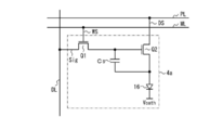
- FIG. 2 is a circuit diagram showing an example of the circuit configuration of the sub-pixel 4a.
- the pixel array unit 5 has a plurality of scanning lines WL extending in the row direction, a plurality of power supply lines PL, and a plurality of data lines DL extending in the column direction. Although not shown, one end of the data line DL is connected to the data line driving unit 15, one end of the scanning line WL is connected to the scanning line driving unit 13, and one end of the power supply line PL is connected to the power supply line driving unit 14. ing.
- Each sub-pixel 4a is arranged at the intersection of the scanning line WL and the data line DL.
- the power supply line driving unit 14 controls the light emission of the sub pixel 4a by sequentially supplying the power supply signal DS to the plurality of power supply line PLs according to the control signals supplied from the timing control unit 12.
- the power supply signal DS transitions between the drive voltage and the initialization voltage.
- the initialization voltage is a voltage for initializing the sub-pixel 4a
- the drive voltage is a voltage for passing a current Ids through the drive transistor DRTr to cause the self-luminous element to emit light.
- the sub-pixel 4a includes a writing transistor Q1, a driving transistor Q2, a self-luminous element 16 such as an organic EL element, and a capacitance element Cs. That is, in this example, the sub-pixel 4a has a so-called "2Tr1C" configuration in which two transistors (writing transistor Q1 and driving transistor Q2) and one capacitive element Cs are used, but other configurations are used. Can also be taken.
- the write transistor Q1 and the drive transistor Q2 are composed of, for example, an N-channel MOS (Metal Oxide Semiconductor) type TFT (Thin Film Transistor).
- MOS Metal Oxide Semiconductor
- the gate is connected to the scanning line WL
- the source is connected to the data line DL
- the drain is connected to the gate of the drive transistor Q2 and one end of the capacitive element Cs.
- the drive transistor Q2 the gate is connected to the drain of the writing transistor Q1 and one end of the capacitive element Cs
- the drain is connected to the power supply line PL
- the source is connected to the other end of the capacitive element Cs and the anode of the self-luminous element 16. ing.
- the self-luminous element 16 is a light emitting element configured by using an organic EL element, an anode is connected to the source of the drive transistor Q2 and the other end of the capacitive element Cs, and a voltage Vcath, which is a DC voltage, is supplied to the cathode. Has been done.
- the self-luminous element 16 emits white light. That is, in this example, as will be described later, the sub-pixel 4a emits red (R), green (G), and blue (B) light by providing a self-luminous element 16 that emits white light and a color filter. Generate each.
- a color filter of a color other than RGB may be provided so that sub-pixels of four or more colors form one pixel.
- the self-luminous element 16 three or more types of self-luminous elements 16 that emit light in different emission colors such as red, green, and blue may be provided in the sub-pixel 4a in the pixel 4. In this case, the color filter is not always necessary.
- the display control unit 6 writes the pixel voltage Vsig to each sub-pixel 4a within one horizontal period.
- the self-luminous element 16 emits light with a brightness corresponding to the written pixel voltage Vsig.
- the display control unit 6 can drive by thinning out a plurality of pixels 4 in consecutive individual frames, and the thinned out pixels 4 are different for each frame. Further, the display control unit 6 can drive all of the plurality of pixels 4 in a plurality of consecutive frames. In this way, the display control unit 6 can drive a part of the pixels 4 that are different for each frame, and can drive all of the plurality of pixels 4 in the plurality of frames.
- the display control unit 6 drives all of the plurality of pixels 4 in a plurality of frames in the thinned out drive display area.
- the display control unit 6 can make the pixel 4 to emit light out of the plurality of pixels 4 different from each other in each frame in a plurality of consecutive frames.
- the display control unit 6 can emit light from one of two adjacent pixels 4 in one of two consecutive frames and emit light from the other of two adjacent pixels 4 in the other of the two adjacent frames. ..
- the display control unit 6 can drive by thinning out a plurality of sub-pixels 4a in the individual pixels 4 in each frame in a plurality of consecutive frames.
- the sub-pixels 4a to be thinned out are different for each frame, and all of the plurality of sub-pixels 4a in the individual pixels 4 can be driven by a plurality of consecutive frames.
- the display control unit 6 can make at least a part of the sub-pixels 4a that do not emit light out of the plurality of sub-pixels 4a different from each other in each frame in the plurality of consecutive frames.
- the display control unit 6 can make the colors to be displayed different between one of the two adjacent pixels 4 and the other in each frame in a plurality of consecutive frames. For example, the display control unit 6 can make the display colors of the individual pixels 4 different in a plurality of consecutive frames. Further, the display control unit 6 can make the pixels 4 displayed in black different from each other in a plurality of consecutive frames. For example, the display control unit 6 can make the sub-pixels 4a displayed in black among the plurality of sub-pixels 4a in the individual pixels 4 different from each other in a plurality of consecutive frames.
- the display control unit 6 When displaying a still image on a plurality of pixels 4, the display control unit 6 displays the still image at a full display resolution in a plurality of consecutive frames, and at each frame, the still image is stationary at a display resolution lower than the full display resolution. Images can be displayed. For example, when the display control unit 6 drives all of the plurality of pixels 4 in N consecutive frames (N is an integer of 2 or more), the brightness in each frame is the brightness of the plurality of pixels 4 in one frame. It is 1 / N of the brightness when driving everything.
- FIGS. 3A, 3B and 3C are diagrams for explaining the first driving method of the display control unit 6.
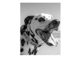
- 3A to 3C show an example in which the full-resolution still image shown in FIG. 3D is thinned out and displayed.
- all the pixels 4 in the display area to be thinned out in the pixel array unit 5 are driven by two consecutive frames.
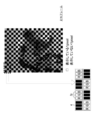
- FIG. 3A shows an example of a still image displayed on the pixel array unit 5 at the time of 2N frame
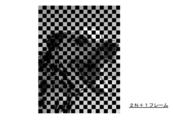
- FIG. 3B shows an example of the still image displayed on the pixel array unit 5 at the time of 2N + 1 frame.
- FIG. 3C is a superposition of the images of FIGS. 3A and 3B.
- the display control unit 6 drives one of the two adjacent pixels 4 in each frame, and does not drive the other. More specifically, in either of the two pixels 4 adjacent in the horizontal direction and the two pixels 4 adjacent in the vertical direction, one pixel 4 is driven and the other pixel 4 is not driven.
- the black pixel 4 indicates a non-driven pixel 4.
- An enlarged view of a 4 ⁇ 2 pixel pixel block at the upper right end is shown in the lower right of FIG. 3A. As can be seen from this enlarged view, one of the two pixels 4 adjacent in the horizontal direction and one of the two pixels 4 adjacent in the vertical direction are black pixels 4.
- the black pixels 4 are arranged in a staggered pattern in the horizontal and vertical directions.
- the display control unit 6 prevents the pixel 4 driven by one of the two consecutive frames from being driven by the other. As a result, as shown in FIG. 3C, all the pixels 4 are driven by two consecutive frames.
- the display resolution in each frame is half that when all pixels are driven. Since the corresponding self-luminous element 16 is not emitted from the non-driven pixel 4, the number of self-luminous elements 16 to be emitted can be halved in each frame, and the power consumption can be significantly reduced.
- the display resolution in each frame is halved, but in another continuous frame, the adjacent pixels 4 are made to emit light to display another still image, so that a human being is used. Since an afterimage remains in the eyes, it is possible for a human to recognize that a still image having a display resolution equivalent to that when all the pixels are driven is displayed. Therefore, according to the first driving method, when displaying a still image on the pixel array unit 5, the still image can be displayed without substantially lowering the display resolution.
- FIGS. 3A and 3B an example is shown in which only one of two adjacent pixels 4 is driven in each frame and the driven pixels 4 are reversed in two consecutive frames.
- One of the adjacent N (N is an integer of 2 or more) pixels 4 may be driven, and the pixels 4 driven by each of the consecutive N frames may be different.
- the still image displayed on the pixel array unit 5 has a brightness of 1 / N at a display resolution of 1 / N for each frame, but the actual display resolution of the still image does not decrease. Further, since the number of self-luminous elements 16 driven by each frame can be reduced to 1 / N, the power consumption can be significantly reduced.
- the brightness is lowered by reducing the number of pixels 4 driven in each frame.
- the light emitting period of each driven pixel 4 is not shortened, there is no possibility that flicker will occur. If it is desired to gradually lower the brightness, the above-mentioned value of N may be gradually increased.
- FIG. 4A, 4B and 4C are diagrams for explaining the second driving method of the display control unit 6.
- the second driving method all the pixels 4 in the display area to be thinned out in the pixel array unit 5 are driven by three consecutive frames.
- FIG. 4A shows an example of a still image displayed on the pixel array unit 5 at the time of 3N frame
- FIG. 4B shows an example of the still image displayed on the pixel array unit 5 at the time of 3N + 1 frame
- FIG. 4C shows an example of the still image displayed on the pixel array unit 5 at the time of 3N + 2 frame.
- An example of the still image displayed in the part 5 is shown.
- the sub-pixels that emit light are marked with R, G, or B, and the sub-pixels that do not emit light are displayed in black.
- the display control unit 6 drives only one of the three sub-pixels 4a of each pixel 4 for each frame, and the remaining two sub-pixels 4a are driven. do not.
- the sub-pixel 4a that is not driven is displayed in black.
- the types of the driven sub-pixels 4a in each pixel 4 are different between the continuous frames. All sub-pixels 4a in all pixels are driven by three consecutive frames.
- the display color of the adjacent pixels 4 is different for each frame. More specifically, the display colors of the two horizontally adjacent pixels are different from each other, and the display colors of the two vertically adjacent pixels are also different from each other. As a result, the display resolution at each frame when the still image is displayed on the pixel array unit 5 is reduced to 1/3 as compared with the case where all the pixels are driven, and the brightness is also reduced to 1/3. As described above, the second driving method can lower the brightness as compared with the first driving method.
- the number of self-luminous elements 16 to be driven is reduced to one-third, so that the power consumption can be reduced as compared with the first drive method. Further, since all the pixels are driven by three consecutive frames, the actual display resolution when displaying a still image is the same as when all the pixels are driven even when the second driving method is adopted. ..
- the second drive method it is conceivable to change the display color of the entire frame for each frame. That is, in the 3N frame, only the red sub-pixel 4a is driven for each pixel 4, in the 3N + 1 frame, only the green sub-pixel 4a is driven for each pixel 4, and in the 3N + 2 frame, only the blue sub-pixel is driven for each pixel 4. It is conceivable to drive only 4a. In this case, the actual display resolution of the still image is the same as the display resolution when all pixels are driven, and the brightness can be reduced to 1/3, which is the same as the second driving method shown in FIGS. 4A to 4C. .. However, since color separation may occur when the line of sight is moved, the second driving method shown in FIGS.
- the second drive method it is possible to make the display colors of adjacent pixels 4 in the frame different without changing the hue of the entire frame, and each pixel in the continuous frame.
- the display color of 4 can be changed.
- the brightness can be reduced without lowering the substantial display resolution when displaying a still image and without causing flicker. That is, according to the second driving method, the brightness can be lowered as compared with the first driving method, and the power consumption can be further reduced.
- 5A, 5B, 5C and 5D are diagrams illustrating a third driving method of the display control unit 6.
- the third driving method is a combination of the first driving method and the second driving method.
- FIG. 5A is a diagram illustrating a third driving method.
- the display control unit 6 drives all the pixels in the pixel array unit 5 with six consecutive frames. In each frame, the display control unit 6 drives only one of the two adjacent pixels 4, and does not drive the other pixel 4. Pixels 4 that are not driven are displayed in black. More specifically, one of the two horizontally adjacent pixels 4 is driven, and the other is a black pixel. Similarly, one of the two vertically adjacent pixels 4 is driven, and the other is a black pixel.
- each pixel 4 is driven by only one frame, and the types of pixels 4 driven by each frame are different.
- the display resolution of each frame becomes 1/6 of the still image when all pixels are driven, and the brightness also becomes 1/6.
- the display resolution of the still image in which the six frames are combined is also 1/6, and the brightness is also 1/6.
- the display resolution and brightness perceived by the human eye are the same as the display resolution and brightness of one frame even if the six frames are combined. ..
- FIG. 5B is a diagram showing an example of a still image in which six frames are combined
- FIG. 5C is a diagram showing an example of a still image in each frame
- FIG. 5D is a diagram showing an example of a still image in which six frames are combined. be.
- the display resolution and the brightness of the still image of one frame and the still image of the combination of six frames are the same, which is 1/6 of that when all pixels are driven. Become.
- the brightness can be lowered and the power consumption can be further reduced as compared with the first and second drive methods.
- the display resolution and the brightness when a plurality of frames are combined are the same as the display resolution and the brightness of each frame.
- the pixel data for realizing the first to third drive methods described above may be generated by the display control unit 6 or the host processing unit 3.
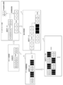
- FIG. 6 is a diagram schematically showing the processing operations of the host processing unit 3 and the display control unit 6 when the pixel array unit 5 normally displays.
- the host processing unit 3 generates a video signal including pixel data and a synchronization signal and transmits the video signal to the display panel unit 2.
- the pixel data included in the video signal may be a digital signal or an analog signal, but the following describes an example in which the host processing unit 3 includes the digitized pixel data in the video signal and transmits it to the display panel unit 2.
- the interface unit 7 of the display panel unit 2 receives the video signal transmitted from the host processing unit 3, separates the data, and extracts the pixel data.
- the extracted pixel data is sent to the display control unit 6.
- the display control unit 6 transmits the pixel data included in the video signal to the data line drive unit 15 without thinning out.
- the data line driving unit 15 once latches the sub-pixel data of each pixel 4 included in the pixel data, and then supplies the sub-pixel data to the corresponding data line DL. As a result, all the pixels of the pixel array unit 5 are driven, and display is performed at a normal display resolution.
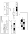
- FIG. 7 is a diagram showing an example in which the display control unit 6 generates pixel data for thinning out the pixels 4.
- FIG. 7 shows an example of adopting the second driving method.
- the processing content of the host processing unit 3 is the same as that of FIG.
- the host processing unit 3 transmits a video signal including pixel data to the display panel unit 2 as in the normal display.
- the interface unit 7 of the display panel unit 2 extracts pixel data from the received video signal and transmits the extracted pixel data to the display control unit 6.
- the display control unit 6 discards the pixel data to be thinned out from the received pixel data, and generates new pixel data in which black pixels are assigned to the pixels 4 that are not displayed.
- the black pixel 4 indicates that the self-luminous element 16 in the corresponding pixel 4 is not emitted.
- the pixel data generated by the display control unit 6 is transmitted to the data line drive unit 15.
- the data line driving unit 15 latches the received pixel data once and then supplies the received pixel data to the corresponding data line DL. As a result, as shown in FIG. 7, one of the two adjacent pixels 4 emits light for each frame, and the other does not emit light.
- FIG. 7 shows an example in which the display control unit 6 performs the processing of thinning out some pixels
- the interface unit 7 may perform the processing of thinning out the pixels.
- FIG. 7 shows an example in which the second drive method is adopted, but the case where the first drive method is adopted is also included in the video signal sent from the host processing unit 3 in the same format as the normal display.
- the pixel data is processed by the display control unit 6. More specifically, the display control unit 6 generates pixel data in which some pixels are thinned out and replaced with black pixels, and the data line driving unit 15 drives the corresponding data line DL based on the pixel data. ..
- FIG. 8 is a diagram showing an example in which the host processing unit 3 performs a process of thinning out a part of the pixels 4.
- FIG. 8 shows an example of adopting the second driving method.
- the host processing unit 3 generates a video signal including pixel data obtained by thinning out some pixels 4.
- the host processing unit 3 discards the pixel data to be thinned out from the pixel data displayed at the time of normal display so that the black pixel is displayed at the position of the pixel data to be thinned out.
- the black pixel data is data indicating that the self-luminous element 16 in the corresponding pixel 4 does not emit light.
- the video signal generated by the host processing unit 3 is received by the interface unit 7 of the display panel unit 2.
- the interface unit 7 extracts the pixel data included in the video signal and transmits the extracted pixel data to the display control unit 6.
- the display control unit 6 transmits the received pixel data to the data line driving unit 15 without processing the received pixel data.
- the data line driving unit 15 latches the received pixel data once and then supplies the received pixel data to the corresponding data line DL.
- FIG. 8 pixel display conforming to the second driving method is performed as in FIG. 7.
- FIG. 8 shows an example in which the second drive method is adopted. Similarly, when the first drive method is adopted, the host processing unit 3 displays a video signal including pixel data conforming to the first drive method. Will be generated.
- FIG. 9 is a diagram showing an example in which the display control unit 6 generates pixel data for thinning out the pixels 4 by adopting the third drive method.
- the processing content of the host processing unit 3 is the same as that of FIG.
- the interface unit 7 of the display panel unit 2 receives the video signal transmitted from the host processing unit 3 and extracts pixel data from the received video signal.
- the interface unit 7 discards the pixel data to be thinned out of the pixel data, and slows down the frequency of the pixel data by the amount of the discarded pixels. For example, when half of the number of pixels 4 is thinned out, the frequency of the pixel data is reduced to 1/2, and the pixel data is transmitted to the display control unit 6.
- the display control unit 6 sends the pixel data transmitted from the interface unit 7 to the data line drive unit 15.
- the data line driving unit 15 latches the received pixel data once and then supplies the received pixel data to the corresponding data line DL. At that time, the data line driving unit 15 controls the timing of the pixel data so that the black pixels are displayed between the pixel data. As a result, pixel display conforming to the third driving method is performed.
- FIG. 9 shows an example in which the interface unit 7 thins out a part of the pixels 4 and the frequency of the pixel data is lowered, but at least one of the processes may be performed by the display control unit 6.
- FIG. 10 is a diagram showing an example in which the third drive method is adopted and the host processing unit 3 generates pixel data for thinning out the pixels 4.
- FIG. 10 shows an example of adopting the third driving method.
- the host processing unit 3 generates a video signal including pixel data obtained by thinning out some pixels 4. More specifically, the host processing unit 3 generates pixel data in which the thinned-out pixel data is discarded, and slows down the frequency of the pixel data by the amount of the thinned-out pixel data.
- the interface unit 7 extracts the pixel data included in the video signal and displays the extracted pixel data in the display control unit 6. Send to.
- the display control unit 6 supplies pixel data to the data line drive unit 15.
- the data line driving unit 15 controls the timing of pixel data so that black pixels are displayed between the pixel data.
- the data line driving unit 15 supplies the timing-controlled pixel data to the corresponding data line DL. As a result, pixel display conforming to the third driving method is performed.
- a plurality of pixels 4 are thinned out and driven in consecutive individual frames, and the pixels 4 to be thinned out are different for each frame. Therefore, all the pixels can be driven in a plurality of frames. , The brightness can be reduced without substantially reducing the display resolution of the still image. In the present embodiment, since the light emitting period of the self-luminous element 16 is not shortened, there is no possibility that flicker will occur even if the brightness is lowered.
- each pixel 4 is composed of a plurality of sub-pixels 4a having different emission colors
- the emission colors are different among the plurality of adjacent pixels 4, and each pixel 4 emits light in a plurality of consecutive frames. Since the colors are different, there is no possibility that the chromaticity of the still image and the moving image will change even when the pixels 4 are thinned out.
- the brightness of the still image can be gradually increased by changing the value of N. You can switch.
- the present technology can have the following configurations.
- a pixel array unit having a plurality of pixels and A display control unit that drives the plurality of pixels at a predetermined frame frequency is provided.
- the pixel has a plurality of sub-pixels that emit light in different colors.
- the plurality of sub-pixels have a plurality of self-luminous elements whose light emission can be individually controlled.
- the display control unit is a display device that thins out and drives the plurality of pixels in continuous individual frames and makes the thinned out pixels different for each frame.
- the display device according to (1) or (2), wherein the display control unit makes the pixels to be emitted light out of the plurality of pixels in each frame in the plurality of consecutive frames.
- the display control unit emits light from one of two adjacent pixels in one of two consecutive frames, and emits light from the other of two adjacent pixels in the other of the two adjacent frames.
- the display control unit drives the plurality of sub-pixels in the individual pixels by thinning out the plurality of sub-pixels in the individual frames in the continuous plurality of frames, and makes the thinned sub-pixels different for each frame to be continuous.
- the display device according to any one of (1) to (4), wherein all of the plurality of sub-pixels in each pixel are driven by the plurality of frames.
- the display control unit differs at least a part of the sub-pixels that do not emit light from the plurality of sub-pixels in individual frames in the plurality of consecutive frames. .. (7)
- the display control unit causes one and the other of two adjacent pixels to display different colors from each other, according to (1) to (6).
- the display device according to any one item.
- the display device according to any one of (1) to (7), wherein the display control unit makes the display colors of individual pixels different in the plurality of consecutive frames.
- the display device according to any one of (1) to (8), wherein the display control unit makes the pixels displayed in black different in the plurality of consecutive frames.
- the display control unit makes the sub-pixels displayed in black among the plurality of sub-pixels in each pixel different from each other in the plurality of consecutive frames.
- the display device according to item 1.
- the display control unit displays the still image at the full display resolution in the plurality of consecutive frames, and in each frame, the still image is higher than the full display resolution.
- the display device according to any one of (1) to (10), which displays the still image at a low display resolution.
- the display control unit drives all of the plurality of pixels in the display area to be thinned out in N consecutive frames (N is an integer of 2 or more), the brightness in each frame is determined.
- a video signal generation unit that generates a video signal including pixel data displayed on the pixel array unit, and A display panel unit having the pixel array unit and the display control unit is provided.
- the display control unit generates the pixel data for the display control unit to thin out and drive the plurality of pixels based on the first pixel data, any one of (1) to (12).
- the pixel data included in the video signal is data on the assumption that the display control unit drives the plurality of pixels without thinning out.
- the display control unit discards signals unnecessary for driving the plurality of pixels in the video signal, and displays black pixels during the period when the plurality of pixels are not driven.
- a video signal generation unit that generates a video signal including pixel data assuming that the display control unit is driven by thinning out the plurality of pixels in continuous individual frames.
- a display panel unit having the pixel array unit and the display control unit is provided.
- the display control unit drives the plurality of pixels by thinning out the plurality of pixels in consecutive individual frames based on the pixel data corresponding to the video signal.
- the display control unit generates pixel data so that black pixels are displayed during a period in which the plurality of pixels are not driven.
- the video signal generation unit or the display control unit adjusts the drive frequency of the pixel data according to the frame frequency.
- Each of the plurality of self-luminous elements emits white light.
- 1 display device 2 display panel unit, 3 host processing unit, 4 pixels, 5 pixel array unit, 6 display control unit, 7 interface unit, 11 signal processing unit, 12 timing control unit, 13 scanning line drive unit, 14 power supply line Drive unit, 15 data line drive unit, 16 self-luminous element
Landscapes
- Engineering & Computer Science (AREA)
- Physics & Mathematics (AREA)
- Computer Hardware Design (AREA)
- General Physics & Mathematics (AREA)
- Theoretical Computer Science (AREA)
- Multimedia (AREA)
- Signal Processing (AREA)
- Electroluminescent Light Sources (AREA)
- Control Of El Displays (AREA)
- Control Of Indicators Other Than Cathode Ray Tubes (AREA)
- Transforming Electric Information Into Light Information (AREA)
Abstract
[課題]輝度を低下させても表示品質を維持できる表示装置を提供する。 [解決手段]表示装置は、複数の画素を有する画素アレイ部と、前記複数の画素を所定のフレーム周波数で駆動する表示制御部と、を備え、前記画素は、それぞれ異なる色で発光する複数のサブ画素を有し、前記複数のサブ画素は、個別に発光を制御可能な複数の自発光素子を有し、前記表示制御部は、連続した個々のフレームで前記複数の画素を間引いて駆動し、間引かれる画素をフレームごとに相違させる。
Description
本開示は、表示装置に関する。
有機EL(Electroluminescent)素子は自発光素子であり、バックライトが不要であることから、表示パネルを薄くできるとともに消費電力を抑制できる。このため、有機EL素子は、スマートフォン等の携帯機器や大型TVなどに用いられる機会がさらに増えることが予想されている。
有機EL素子等の自発光素子を用いた表示パネルは、自発光素子に与える信号電圧を制御することで輝度調整を行うことができるが、製造ばらつき等により、同一の信号電圧を自発光素子に与えても、必ずしも同一の輝度にはならないという問題がある。
信号電圧を制御する以外に、自発光素子の発光期間を制御することで輝度調整を行うことができる。より具体的には、1フレーム内の自発光素子の発光期間を制御し、輝度を下げたい場合は、発光期間を短くする。
しかしながら、自発光素子の発光期間を短くすると、フリッカが生じるという問題がある。フリッカとは、表示画面が点滅しているように感じられる現象であり、表示品質の低下につながる。
フリッカを抑制する技術として、複数の画素のうち、一部の画素だけを消費電力がゼロの表示、あるいは消費電力が表示データより低い表示にする間引き表示を行う技術が提案されている(特許文献1参照)。
特許文献1に記載の技術は、消費電力の削減と表示品質の向上を目的としており、積極的に輝度を低下させることを想定していない。スマートフォン等では、夜間などに意図的に輝度を低下させたい要望があり、輝度を低下させても表示品質を維持できる技術が望まれている。
本開示では、輝度を低下させても表示品質を維持できる表示装置を提供するものである。
上記の課題を解決するために、本開示によれば、複数の画素を有する画素アレイ部と、 前記複数の画素を所定のフレーム周波数で駆動する表示制御部と、を備え、
前記画素は、それぞれ異なる色で発光する複数のサブ画素を有し、
前記複数のサブ画素は、個別に発光を制御可能な複数の自発光素子を有し、
前記表示制御部は、連続した個々のフレームで前記複数の画素を間引いて駆動し、間引かれる画素をフレームごとに相違させる、表示装置が提供され。
前記画素は、それぞれ異なる色で発光する複数のサブ画素を有し、
前記複数のサブ画素は、個別に発光を制御可能な複数の自発光素子を有し、
前記表示制御部は、連続した個々のフレームで前記複数の画素を間引いて駆動し、間引かれる画素をフレームごとに相違させる、表示装置が提供され。
前記表示制御部は、連続した複数のフレームで、間引き駆動する表示エリア内の前記複数の画素のすべてを駆動してもよい。
前記表示制御部は、連続した前記複数のフレーム内の個々のフレームでは、前記複数の画素のうち発光させる画素をそれぞれ相違させてもよい。
前記表示制御部は、連続した2つのフレームの一方では隣接する2つの画素の一方を発光させ、隣接する2つのフレームの他方では隣接する2つの画素の他方を発光させてもよい。
前記表示制御部は、連続した前記複数のフレーム内の個々のフレームでは個々の画素内の前記複数のサブ画素を間引いて駆動し、間引かれるサブ画素をフレームごとに相違させ、連続した複数のフレームで個々の画素内の前記複数のサブ画素のすべてを駆動してもよい。
前記表示制御部は、連続した前記複数のフレーム内の個々のフレームでは、前記複数のサブ画素のうち発光させないサブ画素の少なくとも一部をそれぞれ相違させてもよい。
前記表示制御部は、連続した前記複数のフレーム内の個々のフレームでは、隣接する2つの画素の一方と他方とで、表示させる色を互いに相違させてもよい。
前記表示制御部は、連続した前記複数のフレームでは、個々の画素の表示色をそれぞれ相違させてもよい。
前記表示制御部は、連続した前記複数のフレームでは、黒色で表示される画素をそれぞれ相違させてもよい。
前記表示制御部は、連続した前記複数のフレームでは、個々の画素内の前記複数のサブ画素のうち黒色で表示されるサブ画素をそれぞれ相違させてもよい。
前記表示制御部は、前記複数の画素に静止画像を表示させる場合、連続した前記複数のフレームにて前記静止画像をフル表示解像度で表示させ、個々のフレームでは、前記フル表示解像度よりも低い表示解像度で前記静止画像を表示させてもよい。
前記表示制御部が連続したN枚(Nは2以上の整数)のフレームで、間引き駆動する表示エリア内の前記複数の画素のすべてを駆動してもよく、この場合、個々のフレームでの輝度は、1つのフレームで前記複数の画素のすべてを駆動する場合の輝度の1/Nである。
前記画素アレイ部に表示される画素データを含む映像信号を生成する映像信号生成部と、
前記画素アレイ部及び前記表示制御部を有する表示パネル部と、を備え、
前記表示制御部は、前記第1画素データに基づいて、前記表示制御部が前記複数の画素を間引いて駆動するための前記画素データを生成してもよい。
前記画素アレイ部及び前記表示制御部を有する表示パネル部と、を備え、
前記表示制御部は、前記第1画素データに基づいて、前記表示制御部が前記複数の画素を間引いて駆動するための前記画素データを生成してもよい。
前記映像信号に含まれる画素データは、前記表示制御部が前記複数の画素を間引かずに駆動することを想定したデータであり、
前記表示制御部は、間引かれる画素がフレームごとに異なるように、前記映像信号に基づいて前記画素データを生成してもよい。
前記表示制御部は、間引かれる画素がフレームごとに異なるように、前記映像信号に基づいて前記画素データを生成してもよい。
前記表示制御部は、前記映像信号の中で前記複数の画素の駆動に不必要な信号を廃棄するとともに、前記複数の画素を駆動しない期間内は黒色画素が表示されるように前記画素データを生成してもよい。
前記表示制御部が連続した個々のフレームで前記複数の画素を間引いて駆動することを想定した画素データを含む映像信号を生成する映像信号生成部と、
前記画素アレイ部及び前記表示制御部を有する表示パネル部と、を備え、
前記表示制御部は、前記映像信号に応じた画素データに基づいて、連続した個々のフレームで前記複数の画素を間引いて駆動してもよい。
前記画素アレイ部及び前記表示制御部を有する表示パネル部と、を備え、
前記表示制御部は、前記映像信号に応じた画素データに基づいて、連続した個々のフレームで前記複数の画素を間引いて駆動してもよい。
前記表示制御部は、前記複数の画素を駆動しない期間内は黒色画素が表示されるように前記画素データを生成してもよい。
前記映像信号生成部又は前記表示制御部は、フレーム周波数に合わせて前記画素データの駆動周波数を調整してもよい。
前記複数の自発光素子のそれぞれは、白色光を発光し、
前記複数のサブ画素は、前記複数の自発光素子のそれぞれに対応して設けられ、それぞれ異なる色で発光する複数のカラーフィルタを有してもよい。
前記複数のサブ画素は、前記複数の自発光素子のそれぞれに対応して設けられ、それぞれ異なる色で発光する複数のカラーフィルタを有してもよい。
前記複数の自発光素子のそれぞれは、それぞれ異なる発光波長で発光してもよい。
以下、図面を参照して、表示装置の実施形態について説明する。以下では、表示装置の主要な構成部分を中心に説明するが、表示装置には、図示又は説明されていない構成部分や機能が存在しうる。以下の説明は、図示又は説明されていない構成部分や機能を除外するものではない。
図1は本実施形態による表示装置1の概略構成を示すブロック図である。図1の表示装置1の画面サイズは問わない。図1の表示装置1は、据え置き型のTVやPC(Personal Computer)用の表示装置でもよいし、スマートフォン等の携帯機器用の表示装置でもよい。図1の表示装置1は、表示パネル部2とホスト処理部3とを備えている。表示パネル部2は、二次元平面上に配置される複数の画素4に静止画像又は動画像を表示するものである。ホスト処理部3は、表示パネル部2の複数の画素4に表示するべき画素データを含む映像信号を生成して、表示パネル部2に供給する。ホスト処理部3は、PCやサーバ、ワークステーションなどで構成可能である。表示パネル部2とホスト処理部3は、有線又は無線により映像信号の送受を行う。ホスト処理部3は、表示パネル部2とは離隔して配置されていてもよいし、表示パネル部2の裏面等に取り付けてもよい。
表示パネル部2は、画素アレイ部5と、表示制御部6と、インタフェース部7とを備えている。画素アレイ部5、表示制御部6及びインタフェース部7は、同一の基板上に設けられている。より具体的には、画素アレイ部5は、基板上に半導体プロセス技術を利用して形成されている。表示制御部6とインタフェース部7は、基板上に半導体プロセス技術を利用して形成されてもよいし、あるいはチップ化された表示制御部6やインタフェース部7を基板上に実装してもよい。表示パネル部2は、TVやPCのモニタ、スマートフォン等の直接視認する表示画面を有するものでだけでなく、表示パネル部2の画像を投射した投射画面を視認するマイクロディスプレイでもよい。マイクロディスプレイの一例としては、単結晶シリコン基板上に形成されるOLED(Organic Light Emitting Diode)である。
画素アレイ部5は、二次元平面上に配置される複数の画素4を有する。画素アレイ部5内の画素4の数には特に制限はないが、例えば2k(1920×1080画素)でもよいし、4k(3840×2160画素)でもよいし、それ以外でもよい。
各画素4は、それぞれ異なる色で発光する複数のサブ画素4aを有する。複数のサブ画素4aは、例えばR(赤)、G(緑)、B(青)画素を含む。あるいは、サブ画素4aは、W(白)画素を含んでいてもよいし、それ以外の色の画素を含んでいてもよい。
各画素4内の複数のサブ画素4aは、個別に発光を制御可能な複数の自発光素子を有する。ここで、自発光素子とは、バックライトを設けなくても、サブ画素4aの単位である素子が自ら発光するものである。自発光素子の一代表例は、有機EL素子である。なお、自発光素子は、プラズマディスプレイ素子でもよいし、FED(Field Emission Display)素子でもよい。以下では、自発光素子として有機EL素子を用いる例を主に説明する。
表示制御部6は、画素アレイ部5内の複数の画素4を所定のフレーム周波数で駆動する。フレーム周波数は変更できるようにしてもよい。なお、フレームとは、画素アレイ部5の全画素を指す。フレーム周波数とは、画素アレイ部5内の複数の画素4のすべてを駆動する周波数である。
表示制御部6は、信号処理部11と、タイミング制御部12と、走査線駆動部13と、電源線駆動部14と、データ線駆動部15とを有する。
信号処理部11は、ホスト処理部3から送信された映像信号に基づいて画素データを生成して、データ線駆動部15に供給する。後述するように、信号処理部11の処理内容は、ホスト処理部3から送信される映像信号の信号形式によって変わりうる。信号処理部11からデータ線駆動部15に送られる画素データのデータ形式は、通常表示を行う場合と、間引き表示を行う場合とで異なる。間引き表示とは、一部の画素の表示を行わないことを示し、例えば一部の画素を黒色画素に置換した表示を行う。また、信号処理部11は、ホスト処理部3から送信された映像信号に対して、ガンマ補正等の既存の信号処理を行ってもよい。
タイミング制御部12は、ホスト処理部3等から供給される同期信号に基づいて、走査線駆動部13、電源線駆動部14及びデータ線駆動部15を同期化するための制御信号を生成し、この制御信号を走査線駆動部13、電源線駆動部14及びデータ線駆動部15に供給する。
走査線駆動部13は、タイミング制御部12からの制御信号に従って、複数の走査線に対して走査信号を順次供給して、サブ画素4aを順次選択する。
データ線駆動部15は、信号処理部11から供給された映像信号Sdisp2およびタイミング制御部12から供給された制御信号に従って、各サブ画素4aの発光輝度を指示する画素電圧Vsigを含む信号Sigを生成して、各データ線DLに印加する。
インタフェース部7は、ホスト処理部3からの映像信号を受信して、表示制御部6に送信する処理を行う。場合によっては、インタフェース部7は、パラレル/シリアルデータの変換を行った上で、映像信号に含まれる画素データを表示制御部6に供給する。
図2はサブ画素4aの回路構成の一例を表す回路図である。画素アレイ部5は、行方向に延伸する複数の走査線WLおよび複数の電源線PLと、列方向に延伸する複数のデータ線DLとを有する。図示していないが、データ線DLの一端はデータ線駆動部15に接続され、走査線WLの一端は走査線駆動部13に接続され、電源線PLの一端は電源線駆動部14に接続されている。各サブ画素4aは、走査線WLとデータ線DLとの交差部に配置されている。電源線駆動部14は、タイミング制御部12から供給された制御信号に従って、複数の電源線PLに対して電源信号DSを順次供給することにより、サブ画素4aの発光を制御する。電源信号DSは、駆動電圧と初期化電圧との間で遷移する。初期化電圧は、サブ画素4aを初期化するための電圧であり、駆動電圧は、駆動トランジスタDRTrに電流Idsを流して自発光素子を発光させるための電圧である。
サブ画素4aは、書込トランジスタQ1と、駆動トランジスタQ2と、有機EL素子等の自発光素子16と、容量素子Csとを備えている。すなわち、この例では、サブ画素4aは、2つのトランジスタ(書込トランジスタQ1、駆動トランジスタQ2)および1つの容量素子Csを用いて構成される、いわゆる「2Tr1C」の構成を有するが、その他の構成も取り得る。
書込トランジスタQ1および駆動トランジスタQ2は、例えば、NチャネルMOS(Metal Oxide Semiconductor)型のTFT(Thin Film Transistor;薄膜トランジスタ)により構成される。書込トランジスタQ1は、ゲートが走査線WLに接続され、ソースがデータ線DLに接続され、ドレインが駆動トランジスタQ2のゲートおよび容量素子Csの一端に接続されている。駆動トランジスタQ2は、ゲートが書込トランジスタQ1のドレインおよび容量素子Csの一端に接続され、ドレインが電源線PLに接続され、ソースが容量素子Csの他端および自発光素子16のアノードに接続されている。
容量素子Csは、一端が駆動トランジスタQ2のゲート等に接続され、他端は駆動トランジスタQ2のソース等に接続されている。自発光素子16は、有機EL素子を用いて構成された発光素子であり、アノードが駆動トランジスタQ2のソースおよび容量素子Csの他端に接続され、カソードには、直流電圧である電圧Vcathが供給されている。この自発光素子16は、白色の光を発光するものである。すなわち、この例では、サブ画素4aは、後述するように、白色の光を発する自発光素子16とカラーフィルタを設けることにより、赤色(R)、緑色(G)、青色(B)の光をそれぞれ生成する。RGB以外の色のカラーフィルタを設けて、4色以上のサブピクセルが1画素を構成するようにしてもよい。なお、自発光素子16として、赤色、緑色、青色等の異なる発光色で発光する3種類以上の自発光素子16を画素4内のサブ画素4aに設けてもよい。この場合、カラーフィルタは必ずしも必要なくなる。
本実施形態による表示制御部6は、後述するように、1水平期間内において、各サブ画素4aに対して画素電圧Vsigの書込みを行う。これにより、自発光素子16は、書き込まれた画素電圧Vsigに応じた輝度で発光する。
表示制御部6は、連続した個々のフレームで複数の画素4を間引いて駆動することができ、間引かれる画素4がフレームごとに異なっている。また、表示制御部6は、連続した複数のフレームで複数の画素4のすべてを駆動することができる。このように、表示制御部6は、フレームごとにそれぞれ異なる一部の画素4を駆動し、複数のフレームで複数の画素4のすべてを駆動することができる。なお、表示制御部6は、表示画面内の一部の表示エリアについて間引き駆動する場合、間引き駆動する表示エリアでは、複数のフレームで複数の画素4のすべてを駆動する。
より具体的には、表示制御部6は、連続した複数のフレーム内の個々のフレームでは、複数の画素4のうち発光させる画素4をそれぞれ相違させることができる。例えば、表示制御部6は、連続した2つのフレームの一方では隣接する2つの画素4の一方を発光させ、隣接する2つのフレームの他方では隣接する2つの画素4の他方を発光させることができる。
表示制御部6は、連続した複数のフレーム内の個々のフレームでは個々の画素4内の複数のサブ画素4aを間引いて駆動できる。この場合、間引かれるサブ画素4aがフレームごとに異なっており、連続した複数のフレームで個々の画素4内の複数のサブ画素4aのすべてを駆動することができる。より具体的には、表示制御部6は、連続した複数のフレーム内の個々のフレームでは、複数のサブ画素4aのうち発光させないサブ画素4aの少なくとも一部をそれぞれ相違させることができる。
表示制御部6は、連続した複数のフレーム内の個々のフレームでは、隣接する2つの画素4の一方と他方とで、表示させる色を互いに相違させることができる。例えば、表示制御部6は、連続した複数のフレームでは、個々の画素4の表示色をそれぞれ相違させることができる。また、表示制御部6は、連続した複数のフレームでは、黒色で表示される画素4をそれぞれ相違させることができる。例えば、表示制御部6は、連続した複数のフレームでは、個々の画素4内の複数のサブ画素4aのうち黒色で表示されるサブ画素4aをそれぞれ相違させることができる。
表示制御部6は、複数の画素4に静止画像を表示させる場合、連続した複数のフレームにて静止画像をフル表示解像度で表示させ、個々のフレームでは、フル表示解像度よりも低い表示解像度で静止画像を表示させることができる。例えば、表示制御部6が連続したN枚(Nは2以上の整数)のフレームで複数の画素4のすべてを駆動する場合、個々のフレームでの輝度は、1つのフレームで複数の画素4のすべてを駆動する場合の輝度の1/Nである。
上述したように、表示制御部6が行う複数の画素4の駆動方法には、複数通りが考えられる。以下では、代表的な3つの駆動方法(以下、第1~第3駆動方法)を順に説明する。
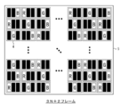
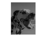
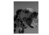
図3A、図3B及び図3Cは表示制御部6の第1駆動方法を説明する図である。図3A~図3Cは、図3Dに示すフル解像度の静止画像を間引いて表示する例を示している。第1駆動方法では、連続する2つのフレームで画素アレイ部5内の間引き駆動する表示エリア内のすべての画素4を駆動するものである。図3Aは2Nフレーム時に画素アレイ部5に表示される静止画像の一例を示し、図3Bは2N+1フレーム時に画素アレイ部5に表示される静止画像の一例を示している。図3Cは、図3Aと図3Bの画像を重ね合わせたものである。
表示制御部6は、各フレームで、隣接する2つの画素4の一方を駆動し、他方は駆動しないようにする。より具体的には、水平方向に隣接する2つの画素4と、垂直方向に隣接する2つの画素4のいずれにおいても、一方の画素4を駆動し、他方の画素4は駆動しないようにする。図3Aと図3Bにおいて、黒色の画素4は駆動していない画素4を示している。図3Aの右下には、右上端の4×2画素の画素ブロックの拡大図が示されている。この拡大図からわかるように、横方向に隣接する2つの画素4の一方と、縦方向に隣接する2つの画素4の一方は黒色の画素4である。黒色の画素4は、横と縦方向に千鳥状に配置されている。
また、表示制御部6は、連続する2つのフレームの一方で駆動した画素4を、他方では駆動しないようにしている。これにより、図3Cに示すように、連続した2つのフレームで、すべての画素4を駆動することになる。
各フレームでの表示解像度は、全画素を駆動した場合の1/2になる。駆動しない画素4については、対応する自発光素子16を発光させないため、各フレームともに、発光させる自発光素子16の数を半減することができ、消費電力を大幅に削減できる。
画素アレイ部5に静止画像を表示する場合、各フレームでの表示解像度は1/2になるが、連続する別のフレームでは隣接する画素4を発光させて別の静止画像を表示するため、人間の目には残像が残ることから、全画素を駆動した場合と同等の表示解像度の静止画像が表示されているものと人間に認識させることができる。よって、第1駆動方法によれば、画素アレイ部5に静止画像を表示する場合に、実質的な表示解像度を低下させることなく、静止画像を表示できる。
ただし、各フレームで駆動している画素4数が半分になるため、図3Cと図3Dを比較すればわかるように、静止画像全体の輝度は、全画素を駆動した場合に比べて1/2に低くなる。
一方、画素アレイ部5に動画像を表示する場合、各フレームでの表示解像度が1/2になるため、動画像全体の表示解像度も1/2になるが、人間の目は動画像の表示解像度の低下に気づきにくいため、画質が劣化したことを認識されるおそれはない。
図3Aと図3Bでは、各フレームで、隣接する2つの画素4の一方のみを駆動するとともに、連続する2つのフレームで、駆動する画素4を逆にする例を示したが、各フレームで、隣接するN(Nは2以上の整数)個の画素4のうち1つを駆動し、連続するN枚のフレームのそれぞれで駆動する画素4を相違させてもよい。この場合、画素アレイ部5に表示される静止画像は、各フレームごとに1/Nの表示解像度で1/Nの輝度になるものの、実質的な静止画像の表示解像度は低下しない。また、各フレームで駆動される自発光素子16の数を1/Nに減らせることから、消費電力を大幅に削減できる。
第1駆動方法では、各フレームで駆動する画素4の数を減らすことで、輝度を低下させている。ただし、駆動する各画素4の発光期間を短くするわけではないため、フリッカが生じるおそれはない。輝度を段階的に低くしたい場合は、上述したNの値を段階的に大きくすればよい。
このように、第1駆動方法を採用することで、静止画像を表示する場合の実質的な表示解像度を落とすことなく、またフリッカを生じさせることなく輝度を低下させることができ、また消費電力も削減できる。
図4A、図4B及び図4Cは表示制御部6の第2駆動方法を説明する図である。第2駆動方法では、連続する3つのフレームで画素アレイ部5内の間引き駆動する表示エリア内のすべての画素4を駆動するものである。図4Aは3Nフレーム時に画素アレイ部5に表示される静止画像の一例を示し、図4Bは3N+1フレーム時に画素アレイ部5に表示される静止画像の一例を示し、図4Cは3N+2フレーム時に画素アレイ部5に表示される静止画像の一例を示している。
図4A~図4Cでは、発光するサブ画素にR、G又はBの記号を付しており、発光させないサブ画素を黒色で表示している。図4A~図4Cからわかるように、表示制御部6は、フレームごとに、各画素4の3つのサブ画素4aのうち、一つのみを駆動しており、残りの2つのサブ画素4aは駆動しない。駆動しないサブ画素4aは、黒色で表示される。また、連続したフレーム同士では、各画素4内の駆動されるサブ画素4aの種類が異なる。連続した3つのフレームにて、全画素内の全サブ画素4aが駆動されることになる。
第2駆動方法では、フレームごとに、隣接する画素4同士の表示色が相違する。より具体的には、水平方向に隣接する2つの画素では表示色が互いに相違しており、また、垂直方向に隣接する2つの画素でも表示色が互いに相違している。これにより、画素アレイ部5に静止画像を表示する場合の各フレームでの表示解像度は、全画素を駆動する場合と比べて1/3になり、輝度も1/3に低下する。このように、第2駆動方法は、第1駆動方法よりも、輝度を下げることができる。
第2駆動方法では、駆動される自発光素子16の数が1/3になるため、第1駆動方法よりも消費電力を削減できる。また、連続した3枚のフレームで全画素を駆動するため、静止画像を表示する場合の実質的な表示解像度は、第2駆動方法を採用した場合でも、全画素を駆動した場合と同等になる。
第2駆動方法の変形例として、フレームごとにフレーム全体の表示色を変えることも考えられる。すなわち、3Nフレームでは、画素4ごとに赤色のサブ画素4aのみを駆動し、3N+1フレームでは、画素4ごとに緑色のサブ画素4aのみを駆動し、3N+2フレームでは、画素4ごとに青色のサブ画素4aのみを駆動することが考えられる。この場合、静止画像の実質的な表示解像度は、全画素駆動時の表示解像度と同等になり、輝度を1/3に削減できる点も図4A~図4Cに示す第2駆動方法と同様である。ただし、視線を動かしたときに色分解を生じさせるおそれがあるため、実用性の観点からは、図4A~図4Cに示す第2駆動方法の方が優れている。図4A~図4Cに示す第2駆動方法では、フレームごとに、隣接する画素4の表示色を変えているが、各フレームの静止画像は複数の色成分を含んでいるため、視線を動かしても、色分解を生じさせるおそれはない。
このように、第2駆動方法を採用することで、フレーム全体としての色合いを変化させることなく、フレーム内の隣接する画素4の表示色を相違させることができ、かつ連続したフレーム内の各画素4の表示色を相違させることができる。これにより、第1駆動方法と同様に、静止画像を表示する場合の実質的な表示解像度を落とすことなく、またフリッカを生じさせることなく輝度を低下させることができる。すなわち、第2の駆動方法によれば、第1の駆動方法よりも輝度を低下させることができ、消費電力もより削減できる。
図5A、図5B、図5C及び図5Dは表示制御部6の第3駆動方法を説明する図である。第3駆動方法は、第1駆動方法と第2駆動方法を組み合わせたものである。
図5Aは第3駆動方法を説明する図である。図5Aの例では、表示制御部6は、連続した6枚のフレームで、画素アレイ部5内の全画素を駆動する。表示制御部6は、各フレームでは、隣接する2つの画素4の一方のみを駆動し、他方の画素4は駆動しない。駆動しない画素4は黒色で表示される。より詳細には、水平方向に隣接する2つの画素4の一方を駆動し、他方は黒色の画素にする。同様に、垂直方向に隣接する2つの画素4の一方を駆動し、他方は黒色の画素にする。
連続した6枚のフレーム同士では、各画素4が1フレームだけ駆動され、各フレームで駆動される画素4の種類はそれぞれ相違する。これにより、各フレームの表示解像度は、全画素駆動時の静止画像の1/6になり、輝度も1/6になる。また、6枚のフレームを合わせた静止画像の表示解像度も1/6であり、輝度も1/6になる。第3駆動方法では、各フレームで駆動する画素が異なるため、6枚のフレームを合わせても、人間の目に感じられる表示解像度及び輝度は、1枚のフレームの表示解像度及び輝度と同じである。
図5Bは6枚のフレームを合わせた静止画像の一例を示す図、図5Cは各フレームの静止画像の一例を示す図、図5Dは6枚のフレームを合わせた静止画像の一例を示す図である。図5Bと図5Dを比較すればわかるように、1枚のフレームの静止画像と6枚のフレームを合わせた静止画像では、表示解像度と輝度が同じになり、全画素駆動時の1/6になる。
このように、第3駆動方法を採用することで、第1及び第2駆動方法よりも、輝度を下げることができ、消費電力もより削減できる。また、第3駆動方法では、複数枚のフレームを合わせた場合の表示解像度及び輝度が、各フレームの表示解像度及び輝度と同じになる。
上述した第1~第3駆動方法を実現するための画素データは、表示制御部6が生成してもよいし、ホスト処理部3が生成してもよい。
図6は画素アレイ部5に通常表示を行う場合のホスト処理部3と表示制御部6の処理動作を模式的に示す図である。ホスト処理部3は、画素データと同期信号を含む映像信号を生成して、表示パネル部2に送信する。映像信号に含まれる画素データは、デジタル信号でもアナログ信号でもよいが、以下では、デジタル化された画素データを映像信号に含めてホスト処理部3が表示パネル部2に送信する例を説明する。
表示パネル部2のインタフェース部7は、ホスト処理部3から送信された映像信号を受信し、データ分離を行って、画素データを抽出する。抽出された画素データは、表示制御部6に送られる。通常表示を行う場合、表示制御部6は、映像信号に含まれる画素データを間引くことなく、データ線駆動部15に送信する。データ線駆動部15は、画素データに含まれる各画素4のサブ画素データをいったんラッチした後に、対応するデータ線DLに供給する。これにより、画素アレイ部5の全画素が駆動されて、通常の表示解像度で表示が行われる。
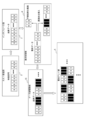
図7は表示制御部6にて画素4を間引くための画素データを生成する例を示す図である。図7は第2駆動方法を採用する例を示している。図7の場合、ホスト処理部3の処理内容は図6と同様である。ホスト処理部3は、通常表示と同様に、画素データを含む映像信号を表示パネル部2に送信する。表示パネル部2のインタフェース部7は、受信した映像信号から画素データを抽出し、抽出された画素データを表示制御部6に送信する。表示制御部6は、受信された画素データのうち、間引く対象の画素データは廃棄するとともに、表示しない画素4には、黒色の画素を割り振った新たな画素データを生成する。黒色の画素4は、対応する画素4内の自発光素子16を発光させないことを示す。表示制御部6で生成された画素データは、データ線駆動部15に送信される。データ線駆動部15は、受信した画素データをいったんラッチした後、対応するデータ線DLに供給する。これにより、図7に示すように、フレームごとに、隣接する2つの画素4の一方は発光され、他方は発光されなくなる。
図7では、表示制御部6にて一部の画素を間引く処理を行う例を示したが、画素を間引く処理をインタフェース部7で行ってもよい。図7では、第2駆動方法を採用する例を示したが、第1駆動方法を採用する場合も同様に、ホスト処理部3から通常表示と同様の形式で送られてきた映像信号に含まれる画素データを表示制御部6で加工する。より具体的には、表示制御部6は一部の画素を間引いて黒色の画素に置換した画素データを生成し、この画素データに基づいてデータ線駆動部15は対応するデータ線DLを駆動する。
図8はホスト処理部3で一部の画素4を間引く処理を行う例を示す図である。図8は第2駆動方法を採用する例を示している。図8では、ホスト処理部3で、一部の画素4を間引いた画素データを含む映像信号を生成する。ホスト処理部3は、通常表示時に表示される画素データの中から、間引かれる画素データを廃棄して、間引かれる画素データの位置には黒色画素が表示されるようにする。黒色の画素データは、対応する画素4内の自発光素子16を発光しないことを示すデータである。
ホスト処理部3で生成された映像信号は、表示パネル部2のインタフェース部7で受信される。インタフェース部7は、映像信号に含まれる画素データを抽出して、抽出された画素データを表示制御部6に送信する。表示制御部6は、受信された画素データを加工することなく、その画素データをデータ線駆動部15に送信する。データ線駆動部15は、受信された画素データをいったんラッチした後に、対応するデータ線DLに供給する。これにより、図8に示すように、図7と同様に、第2駆動方法に準拠した画素表示が行われる。
図8では、第2駆動方法を採用する例を示したが、第1駆動方法を採用する場合も同様に、ホスト処理部3にて、第1駆動方法に準拠した画素データを含む映像信号が生成される。
図9は第3駆動方法を採用して表示制御部6にて画素4を間引くための画素データを生成する例を示す図である。図9の場合、ホスト処理部3の処理内容は図6と同様である。表示パネル部2のインタフェース部7は、ホスト処理部3から送信された映像信号を受信し、受信された映像信号から画素データを抽出する。インタフェース部7は、画素データのうち、間引かれる画素データを廃棄するとともに、画素を廃棄した分だけ、画素データの周波数を遅くする。例えば、画素4数の半分を間引いた場合は、画素データの周波数を1/2に落とした上で、その画素データを表示制御部6に送信する。
表示制御部6は、インタフェース部7から送信された画素データをデータ線駆動部15に送る。データ線駆動部15は、受信された画素データをいったんラッチした上で、対応するデータ線DLに供給する。その際、データ線駆動部15は、画素データの合間に、黒色画素が表示されるように画素データのタイミング制御を行う。これにより、第3駆動方法に準拠した画素表示が行われる。
図9では、インタフェース部7にて一部の画素4を間引く処理と、画素データの周波数を落とす処理を行う例を示したが、少なくとも一方の処理を表示制御部6で行ってもよい。
図10は第3駆動方法を採用してホスト処理部3で画素4を間引くための画素データを生成する例を示す図である。図10は第3駆動方法を採用する例を示している。図10の場合、ホスト処理部3で、一部の画素4を間引いた画素データを含む映像信号を生成する。より具体的には、ホスト処理部3は、間引かれる画素データを廃棄した画素データを生成し、間引いた分だけ、画素データの周波数を遅くする。ホスト処理部3から送信された映像信号が表示パネル部2のインタフェース部7で受信されると、インタフェース部7は映像信号に含まれる画素データを抽出し、抽出された画素データを表示制御部6に送信する。表示制御部6は、データ線駆動部15に画素データを供給する。データ線駆動部15は、画素データの合間に黒色画素が表示されるように画素データのタイミング制御を行う。データ線駆動部15は、タイミング制御を行った画素データを対応するデータ線DLに供給する。これにより、第3駆動方法に準拠した画素表示が行われる。
このように、本実施形態では、連続した個々のフレームで複数の画素4を間引いて駆動し、間引かれる画素4がフレームごとに異なるようにしたため、複数フレームで全画素を駆動することができ、静止画像の表示解像度を実質的に落とすことなく、輝度を低下させることができる。本実施形態では、自発光素子16の発光期間を短くするわけではないので、輝度を低下させても、フリッカが生じるおそれはない。
また、各画素4がそれぞれ発光色の異なる複数のサブ画素4aで構成されている場合には、隣接する複数の画素4で発光色を相違させ、かつ連続した複数のフレームで各画素4の発光色を相違させるため、画素4を間引き駆動した場合であっても、静止画像及び動画像の色度が変化するおそれがない。
さらに、N枚のフレームで全画素を駆動し、N枚のフレーム内の各フレームで駆動する画素4を相違させるようにすれば、Nの値を変えることで、静止画像の輝度を段階的に切り替えることができる。
なお、本技術は以下のような構成を取ることができる。
(1)複数の画素を有する画素アレイ部と、
前記複数の画素を所定のフレーム周波数で駆動する表示制御部と、を備え、
前記画素は、それぞれ異なる色で発光する複数のサブ画素を有し、
前記複数のサブ画素は、個別に発光を制御可能な複数の自発光素子を有し、
前記表示制御部は、連続した個々のフレームで前記複数の画素を間引いて駆動し、間引かれる画素をフレームごとに相違させる、表示装置。
(2)前記表示制御部は、連続した複数のフレームで、間引き駆動する表示エリア内の前記複数の画素のすべてを駆動する、(1)に記載の表示装置。
(3)前記表示制御部は、連続した前記複数のフレーム内の個々のフレームでは、前記複数の画素のうち発光させる画素をそれぞれ相違させる、(1)又は(2)に記載の表示装置。
(4)前記表示制御部は、連続した2つのフレームの一方では隣接する2つの画素の一方を発光させ、隣接する2つのフレームの他方では隣接する2つの画素の他方を発光させる、(2)又は(3)に記載の表示装置。
(5)前記表示制御部は、連続した前記複数のフレーム内の個々のフレームでは個々の画素内の前記複数のサブ画素を間引いて駆動し、間引かれるサブ画素をフレームごとに相違させ、連続した複数のフレームで個々の画素内の前記複数のサブ画素のすべてを駆動する、(1)乃至(4)のいずれか一項に記載の表示装置。
(6)前記表示制御部は、連続した前記複数のフレーム内の個々のフレームでは、前記複数のサブ画素のうち発光させないサブ画素の少なくとも一部をそれぞれ相違させる、(5)に記載の表示装置。
(7)前記表示制御部は、連続した前記複数のフレーム内の個々のフレームでは、隣接する2つの画素の一方と他方とで、表示させる色を互いに相違させる、(1)乃至(6)のいずれか一項に記載の表示装置。
(8)前記表示制御部は、連続した前記複数のフレームでは、個々の画素の表示色をそれぞれ相違させる、(1)乃至(7)のいずれか一項に記載の表示装置。
(9)前記表示制御部は、連続した前記複数のフレームでは、黒色で表示される画素をそれぞれ相違させる、(1)乃至(8)のいずれか一項に記載の表示装置。
(10)前記表示制御部は、連続した前記複数のフレームでは、個々の画素内の前記複数のサブ画素のうち黒色で表示されるサブ画素をそれぞれ相違させる、(1)乃至(9)のいずれか一項に記載の表示装置。
(11)前記表示制御部は、前記複数の画素に静止画像を表示させる場合、連続した前記複数のフレームにて前記静止画像をフル表示解像度で表示させ、個々のフレームでは、前記フル表示解像度よりも低い表示解像度で前記静止画像を表示させる、(1)乃至(10)のいずれか一項に記載の表示装置。
(12)前記表示制御部が連続したN枚(Nは2以上の整数)のフレームで、間引き駆動する表示エリア内の前記複数の画素のすべてを駆動する場合、個々のフレームでの輝度は、1つのフレームで前記複数の画素のすべてを駆動する場合の輝度の1/Nである、(11)に記載の表示装置。
(13)前記画素アレイ部に表示される画素データを含む映像信号を生成する映像信号生成部と、
前記画素アレイ部及び前記表示制御部を有する表示パネル部と、を備え、
前記表示制御部は、前記第1画素データに基づいて、前記表示制御部が前記複数の画素を間引いて駆動するための前記画素データを生成する、(1)乃至(12)のいずれか一項に記載の表示装置。
(14)前記映像信号に含まれる画素データは、前記表示制御部が前記複数の画素を間引かずに駆動することを想定したデータであり、
前記表示制御部は、間引かれる画素がフレームごとに異なるように、前記映像信号に基づいて前記画素データを生成する、(13)に記載の表示装置。
(15)前記表示制御部は、前記映像信号の中で前記複数の画素の駆動に不必要な信号を廃棄するとともに、前記複数の画素を駆動しない期間内は黒色画素が表示されるように前記画素データを生成する、(13)又は(14)に記載の表示装置。
(16)前記表示制御部が連続した個々のフレームで前記複数の画素を間引いて駆動することを想定した画素データを含む映像信号を生成する映像信号生成部と、
前記画素アレイ部及び前記表示制御部を有する表示パネル部と、を備え、
前記表示制御部は、前記映像信号に応じた画素データに基づいて、連続した個々のフレームで前記複数の画素を間引いて駆動する、(1)乃至(12)のいずれか一項に記載の表示装置。
(17)前記表示制御部は、前記複数の画素を駆動しない期間内は黒色画素が表示されるように画素データを生成する、(16)に記載の表示装置。
(18)前記映像信号生成部又は前記表示制御部は、フレーム周波数に合わせて前記画素データの駆動周波数を調整する、(13)乃至(17)のいずれか一項に記載の表示装置。
(19)前記複数の自発光素子のそれぞれは、白色光を発光し、
前記複数のサブ画素は、前記複数の自発光素子のそれぞれに対応して設けられ、それぞれ異なる色で発光する複数のカラーフィルタを有する、(1)乃至(18)のいずれか一項に記載の表示装置。
(20)前記複数の自発光素子のそれぞれは、それぞれ異なる発光波長で発光する、(1)乃至(18)のいずれか一項に記載の表示装置。
(1)複数の画素を有する画素アレイ部と、
前記複数の画素を所定のフレーム周波数で駆動する表示制御部と、を備え、
前記画素は、それぞれ異なる色で発光する複数のサブ画素を有し、
前記複数のサブ画素は、個別に発光を制御可能な複数の自発光素子を有し、
前記表示制御部は、連続した個々のフレームで前記複数の画素を間引いて駆動し、間引かれる画素をフレームごとに相違させる、表示装置。
(2)前記表示制御部は、連続した複数のフレームで、間引き駆動する表示エリア内の前記複数の画素のすべてを駆動する、(1)に記載の表示装置。
(3)前記表示制御部は、連続した前記複数のフレーム内の個々のフレームでは、前記複数の画素のうち発光させる画素をそれぞれ相違させる、(1)又は(2)に記載の表示装置。
(4)前記表示制御部は、連続した2つのフレームの一方では隣接する2つの画素の一方を発光させ、隣接する2つのフレームの他方では隣接する2つの画素の他方を発光させる、(2)又は(3)に記載の表示装置。
(5)前記表示制御部は、連続した前記複数のフレーム内の個々のフレームでは個々の画素内の前記複数のサブ画素を間引いて駆動し、間引かれるサブ画素をフレームごとに相違させ、連続した複数のフレームで個々の画素内の前記複数のサブ画素のすべてを駆動する、(1)乃至(4)のいずれか一項に記載の表示装置。
(6)前記表示制御部は、連続した前記複数のフレーム内の個々のフレームでは、前記複数のサブ画素のうち発光させないサブ画素の少なくとも一部をそれぞれ相違させる、(5)に記載の表示装置。
(7)前記表示制御部は、連続した前記複数のフレーム内の個々のフレームでは、隣接する2つの画素の一方と他方とで、表示させる色を互いに相違させる、(1)乃至(6)のいずれか一項に記載の表示装置。
(8)前記表示制御部は、連続した前記複数のフレームでは、個々の画素の表示色をそれぞれ相違させる、(1)乃至(7)のいずれか一項に記載の表示装置。
(9)前記表示制御部は、連続した前記複数のフレームでは、黒色で表示される画素をそれぞれ相違させる、(1)乃至(8)のいずれか一項に記載の表示装置。
(10)前記表示制御部は、連続した前記複数のフレームでは、個々の画素内の前記複数のサブ画素のうち黒色で表示されるサブ画素をそれぞれ相違させる、(1)乃至(9)のいずれか一項に記載の表示装置。
(11)前記表示制御部は、前記複数の画素に静止画像を表示させる場合、連続した前記複数のフレームにて前記静止画像をフル表示解像度で表示させ、個々のフレームでは、前記フル表示解像度よりも低い表示解像度で前記静止画像を表示させる、(1)乃至(10)のいずれか一項に記載の表示装置。
(12)前記表示制御部が連続したN枚(Nは2以上の整数)のフレームで、間引き駆動する表示エリア内の前記複数の画素のすべてを駆動する場合、個々のフレームでの輝度は、1つのフレームで前記複数の画素のすべてを駆動する場合の輝度の1/Nである、(11)に記載の表示装置。
(13)前記画素アレイ部に表示される画素データを含む映像信号を生成する映像信号生成部と、
前記画素アレイ部及び前記表示制御部を有する表示パネル部と、を備え、
前記表示制御部は、前記第1画素データに基づいて、前記表示制御部が前記複数の画素を間引いて駆動するための前記画素データを生成する、(1)乃至(12)のいずれか一項に記載の表示装置。
(14)前記映像信号に含まれる画素データは、前記表示制御部が前記複数の画素を間引かずに駆動することを想定したデータであり、
前記表示制御部は、間引かれる画素がフレームごとに異なるように、前記映像信号に基づいて前記画素データを生成する、(13)に記載の表示装置。
(15)前記表示制御部は、前記映像信号の中で前記複数の画素の駆動に不必要な信号を廃棄するとともに、前記複数の画素を駆動しない期間内は黒色画素が表示されるように前記画素データを生成する、(13)又は(14)に記載の表示装置。
(16)前記表示制御部が連続した個々のフレームで前記複数の画素を間引いて駆動することを想定した画素データを含む映像信号を生成する映像信号生成部と、
前記画素アレイ部及び前記表示制御部を有する表示パネル部と、を備え、
前記表示制御部は、前記映像信号に応じた画素データに基づいて、連続した個々のフレームで前記複数の画素を間引いて駆動する、(1)乃至(12)のいずれか一項に記載の表示装置。
(17)前記表示制御部は、前記複数の画素を駆動しない期間内は黒色画素が表示されるように画素データを生成する、(16)に記載の表示装置。
(18)前記映像信号生成部又は前記表示制御部は、フレーム周波数に合わせて前記画素データの駆動周波数を調整する、(13)乃至(17)のいずれか一項に記載の表示装置。
(19)前記複数の自発光素子のそれぞれは、白色光を発光し、
前記複数のサブ画素は、前記複数の自発光素子のそれぞれに対応して設けられ、それぞれ異なる色で発光する複数のカラーフィルタを有する、(1)乃至(18)のいずれか一項に記載の表示装置。
(20)前記複数の自発光素子のそれぞれは、それぞれ異なる発光波長で発光する、(1)乃至(18)のいずれか一項に記載の表示装置。
本開示の態様は、上述した個々の実施形態に限定されるものではなく、当業者が想到しうる種々の変形も含むものであり、本開示の効果も上述した内容に限定されない。すなわち、特許請求の範囲に規定された内容およびその均等物から導き出される本開示の概念的な思想と趣旨を逸脱しない範囲で種々の追加、変更および部分的削除が可能である。
1 表示装置、2 表示パネル部、3 ホスト処理部、4 画素、5 画素アレイ部、6 表示制御部、7 インタフェース部、11 信号処理部、12 タイミング制御部、13 走査線駆動部、14 電源線駆動部、15 データ線駆動部、16 自発光素子
Claims (20)
- 複数の画素を有する画素アレイ部と、
前記複数の画素を所定のフレーム周波数で駆動する表示制御部と、を備え、
前記画素は、それぞれ異なる色で発光する複数のサブ画素を有し、
前記複数のサブ画素は、個別に発光を制御可能な複数の自発光素子を有し、
前記表示制御部は、連続した個々のフレームで前記複数の画素を間引いて駆動し、間引かれる画素をフレームごとに相違させる、表示装置。 - 前記表示制御部は、連続した複数のフレームで、間引き駆動する表示エリア内の前記複数の画素のすべてを駆動する、請求項1に記載の表示装置。
- 前記表示制御部は、連続した前記複数のフレーム内の個々のフレームでは、前記複数の画素のうち発光させる画素をそれぞれ相違させる、請求項1に記載の表示装置。
- 前記表示制御部は、連続した2つのフレームの一方では隣接する2つの画素の一方を発光させ、隣接する2つのフレームの他方では隣接する2つの画素の他方を発光させる、請求項2に記載の表示装置。
- 前記表示制御部は、連続した前記複数のフレーム内の個々のフレームでは個々の画素内の前記複数のサブ画素を間引いて駆動し、間引かれるサブ画素をフレームごとに相違させ、連続した複数のフレームで個々の画素内の前記複数のサブ画素のすべてを駆動する、請求項1に記載の表示装置。
- 前記表示制御部は、連続した前記複数のフレーム内の個々のフレームでは、前記複数のサブ画素のうち発光させないサブ画素の少なくとも一部をそれぞれ相違させる、請求項5に記載の表示装置。
- 前記表示制御部は、連続した前記複数のフレーム内の個々のフレームでは、隣接する2つの画素の一方と他方とで、表示させる色を互いに相違させる、請求項1に記載の表示装置。
- 前記表示制御部は、連続した前記複数のフレームでは、個々の画素の表示色をそれぞれ相違させる、請求項1に記載の表示装置。
- 前記表示制御部は、連続した前記複数のフレームでは、黒色で表示される画素をそれぞれ相違させる、請求項1に記載の表示装置。
- 前記表示制御部は、連続した前記複数のフレームでは、個々の画素内の前記複数のサブ画素のうち黒色で表示されるサブ画素をそれぞれ相違させる、請求項1に記載の表示装置。
- 前記表示制御部は、前記複数の画素に静止画像を表示させる場合、連続した前記複数のフレームにて前記静止画像をフル表示解像度で表示させ、個々のフレームでは、前記フル表示解像度よりも低い表示解像度で前記静止画像を表示させる、請求項1に記載の表示装置。
- 前記表示制御部が連続したN枚(Nは2以上の整数)のフレームで、間引き駆動する表示エリア内の前記複数の画素のすべてを駆動する場合、個々のフレームでの輝度は、1つのフレームで前記複数の画素のすべてを駆動する場合の輝度の1/Nである、請求項11に記載の表示装置。
- 前記画素アレイ部に表示される画素データを含む映像信号を生成する映像信号生成部と、
前記画素アレイ部及び前記表示制御部を有する表示パネル部と、を備え、
前記表示制御部は、前記映像信号に含まれる画素データに基づいて、前記表示制御部が前記複数の画素を間引いて駆動するための画素データを生成する、請求項1に記載の表示装置。 - 前記映像信号に含まれる画素データは、前記表示制御部が前記複数の画素を間引かずに駆動することを想定したデータであり、
前記表示制御部は、間引かれる画素がフレームごとに異なるように、前記映像信号に基づいて前記画素データを生成する、請求項13に記載の表示装置。 - 前記表示制御部は、前記映像信号の中で前記複数の画素の駆動に不必要な信号を廃棄するとともに、前記複数の画素を駆動しない期間内は黒色画素が表示されるように前記画素データを生成する、請求項13に記載の表示装置。
- 前記表示制御部が連続した個々のフレームで前記複数の画素を間引いて駆動することを想定した画素データを含む映像信号を生成する映像信号生成部と、
前記画素アレイ部及び前記表示制御部を有する表示パネル部と、を備え、
前記表示制御部は、前記映像信号に応じた画素データに基づいて、連続した個々のフレームで前記複数の画素を間引いて駆動する、請求項1に記載の表示装置。 - 前記表示制御部は、前記複数の画素を駆動しない期間内は黒色画素が表示されるように画素データを生成する、請求項16に記載の表示装置。
- 前記映像信号生成部又は前記表示制御部は、フレーム周波数に合わせて前記画素データの駆動周波数を調整する、請求項13に記載の表示装置。
- 前記複数の自発光素子のそれぞれは、白色光を発光し、
前記複数のサブ画素は、前記複数の自発光素子のそれぞれに対応して設けられ、それぞれ異なる色で発光する複数のカラーフィルタを有する、請求項1に記載の表示装置。 - 前記複数の自発光素子のそれぞれは、それぞれ異なる発光波長で発光する、請求項1に記載の表示装置。
Applications Claiming Priority (2)
| Application Number | Priority Date | Filing Date | Title |
|---|---|---|---|
| JP2020012822A JP2021117460A (ja) | 2020-01-29 | 2020-01-29 | 表示装置 |
| JP2020-012822 | 2020-01-29 |
Publications (1)
| Publication Number | Publication Date |
|---|---|
| WO2021153328A1 true WO2021153328A1 (ja) | 2021-08-05 |
Family
ID=77078871
Family Applications (1)
| Application Number | Title | Priority Date | Filing Date |
|---|---|---|---|
| PCT/JP2021/001608 Ceased WO2021153328A1 (ja) | 2020-01-29 | 2021-01-19 | 表示装置 |
Country Status (2)
| Country | Link |
|---|---|
| JP (1) | JP2021117460A (ja) |
| WO (1) | WO2021153328A1 (ja) |
Citations (3)
| Publication number | Priority date | Publication date | Assignee | Title |
|---|---|---|---|---|
| JP2012128030A (ja) * | 2010-12-13 | 2012-07-05 | Canon Inc | 表示装置およびその駆動方法 |
| JP2016001290A (ja) * | 2014-06-12 | 2016-01-07 | 株式会社ジャパンディスプレイ | 表示装置 |
| US20190180695A1 (en) * | 2017-12-11 | 2019-06-13 | Samsung Display Co., Ltd. | Display device capable of changing luminance depending on operating frequency |
-
2020
- 2020-01-29 JP JP2020012822A patent/JP2021117460A/ja active Pending
-
2021
- 2021-01-19 WO PCT/JP2021/001608 patent/WO2021153328A1/ja not_active Ceased
Patent Citations (3)
| Publication number | Priority date | Publication date | Assignee | Title |
|---|---|---|---|---|
| JP2012128030A (ja) * | 2010-12-13 | 2012-07-05 | Canon Inc | 表示装置およびその駆動方法 |
| JP2016001290A (ja) * | 2014-06-12 | 2016-01-07 | 株式会社ジャパンディスプレイ | 表示装置 |
| US20190180695A1 (en) * | 2017-12-11 | 2019-06-13 | Samsung Display Co., Ltd. | Display device capable of changing luminance depending on operating frequency |
Also Published As
| Publication number | Publication date |
|---|---|
| JP2021117460A (ja) | 2021-08-10 |
Similar Documents
| Publication | Publication Date | Title |
|---|---|---|
| US11011585B2 (en) | Display panel and display device having an array of sub-pixels and transparent areas, and driving method thereof | |
| KR102594294B1 (ko) | 전계 발광 표시 장치 및 이의 구동 방법 | |
| USRE50395E1 (en) | Electronic apparatus and method for controlling thereof | |
| CN101630498B (zh) | 显示装置、驱动用的集成电路、其驱动方法及信号处理方法 | |
| US7948506B2 (en) | Method and apparatus for defect correction in a display | |
| CN109716425B (zh) | 异步控制显示更新和发光 | |
| KR102516371B1 (ko) | 표시장치와 그 구동 방법 | |
| US20190228713A1 (en) | Display device and electronic apparatus | |
| JP2001265282A (ja) | 画像表示装置及びその駆動方法 | |
| US20160284265A1 (en) | Method of Implementing Global Illumination With OLED Displays | |
| JP2014212080A (ja) | 表示装置 | |
| GB2509383A (en) | Display colour conversion based on grey scale region | |
| US20080297455A1 (en) | Image display device and liquid crystal television | |
| US11302240B2 (en) | Pixel block-based display data processing and transmission | |
| KR20130034740A (ko) | 유기 발광 표시 장치 및 그 구동 방법 | |
| KR102106556B1 (ko) | 타이밍 컨트롤러 및 그 구동 방법과 이를 이용한 표시장치 | |
| US20130016135A1 (en) | Display system and control method thereof | |
| KR102361445B1 (ko) | 표시장치, 그 표시패널 및 그 타이밍 컨트롤러 | |
| CN115311952A (zh) | 具非矩形主动区的显示装置与其像素结构 | |
| KR102725332B1 (ko) | 디스플레이 장치 및 그의 렌더링 방법 | |
| KR102640015B1 (ko) | 표시 장치 및 그 구동 방법 | |
| WO2021153328A1 (ja) | 表示装置 | |
| KR102044133B1 (ko) | 유기발광소자표시장치 및 그 구동방법 | |
| KR102316567B1 (ko) | 전계발광 표시장치 및 그 구동방법 | |
| JP7517777B2 (ja) | 表示装置及び表示装置の駆動方法 |
Legal Events
| Date | Code | Title | Description |
|---|---|---|---|
| 121 | Ep: the epo has been informed by wipo that ep was designated in this application |
Ref document number: 21748004 Country of ref document: EP Kind code of ref document: A1 |
|
| NENP | Non-entry into the national phase |
Ref country code: DE |
|
| 122 | Ep: pct application non-entry in european phase |
Ref document number: 21748004 Country of ref document: EP Kind code of ref document: A1 |