WO2021144851A1 - Schottky barrier diode - Google Patents
Schottky barrier diode Download PDFInfo
- Publication number
- WO2021144851A1 WO2021144851A1 PCT/JP2020/000900 JP2020000900W WO2021144851A1 WO 2021144851 A1 WO2021144851 A1 WO 2021144851A1 JP 2020000900 W JP2020000900 W JP 2020000900W WO 2021144851 A1 WO2021144851 A1 WO 2021144851A1
- Authority
- WO
- WIPO (PCT)
- Prior art keywords
- guard ring
- schottky barrier
- semiconductor substrate
- barrier diode
- inner guard
- Prior art date
Links
- 230000004888 barrier function Effects 0.000 title claims abstract description 77
- 239000004065 semiconductor Substances 0.000 claims abstract description 123
- 239000000758 substrate Substances 0.000 claims abstract description 70
- 239000013078 crystal Substances 0.000 claims description 7
- 230000007547 defect Effects 0.000 claims description 7
- AJNVQOSZGJRYEI-UHFFFAOYSA-N digallium;oxygen(2-) Chemical compound [O-2].[O-2].[O-2].[Ga+3].[Ga+3] AJNVQOSZGJRYEI-UHFFFAOYSA-N 0.000 claims description 3
- 229910001195 gallium oxide Inorganic materials 0.000 claims description 3
- HBMJWWWQQXIZIP-UHFFFAOYSA-N silicon carbide Chemical group [Si+]#[C-] HBMJWWWQQXIZIP-UHFFFAOYSA-N 0.000 claims description 3
- 229910010271 silicon carbide Inorganic materials 0.000 claims description 3
- 229910002601 GaN Inorganic materials 0.000 claims description 2
- JMASRVWKEDWRBT-UHFFFAOYSA-N Gallium nitride Chemical compound [Ga]#N JMASRVWKEDWRBT-UHFFFAOYSA-N 0.000 claims description 2
- 239000010432 diamond Substances 0.000 claims description 2
- 229910003460 diamond Inorganic materials 0.000 claims description 2
- 239000000463 material Substances 0.000 claims description 2
- 229910021420 polycrystalline silicon Inorganic materials 0.000 claims description 2
- 229920005591 polysilicon Polymers 0.000 claims description 2
- 238000009413 insulation Methods 0.000 abstract 3
- BOTDANWDWHJENH-UHFFFAOYSA-N Tetraethyl orthosilicate Chemical compound CCO[Si](OCC)(OCC)OCC BOTDANWDWHJENH-UHFFFAOYSA-N 0.000 description 2
- 229910052710 silicon Inorganic materials 0.000 description 2
- 239000010703 silicon Substances 0.000 description 2
- 108091006146 Channels Proteins 0.000 description 1
- 108010075750 P-Type Calcium Channels Proteins 0.000 description 1
- 230000000052 comparative effect Effects 0.000 description 1
- 230000006378 damage Effects 0.000 description 1
- 238000010586 diagram Methods 0.000 description 1
- 230000000694 effects Effects 0.000 description 1
- 230000005684 electric field Effects 0.000 description 1
- 238000010894 electron beam technology Methods 0.000 description 1
- 239000012535 impurity Substances 0.000 description 1
- 150000002500 ions Chemical class 0.000 description 1
- 238000004519 manufacturing process Methods 0.000 description 1
- 229910052751 metal Inorganic materials 0.000 description 1
- 239000002184 metal Substances 0.000 description 1
- 230000004048 modification Effects 0.000 description 1
- 238000012986 modification Methods 0.000 description 1
- 238000010992 reflux Methods 0.000 description 1
Images


Classifications
-
- H—ELECTRICITY
- H01—ELECTRIC ELEMENTS
- H01L—SEMICONDUCTOR DEVICES NOT COVERED BY CLASS H10
- H01L29/00—Semiconductor devices adapted for rectifying, amplifying, oscillating or switching, or capacitors or resistors with at least one potential-jump barrier or surface barrier, e.g. PN junction depletion layer or carrier concentration layer; Details of semiconductor bodies or of electrodes thereof ; Multistep manufacturing processes therefor
- H01L29/40—Electrodes ; Multistep manufacturing processes therefor
- H01L29/43—Electrodes ; Multistep manufacturing processes therefor characterised by the materials of which they are formed
- H01L29/47—Schottky barrier electrodes
-
- H—ELECTRICITY
- H01—ELECTRIC ELEMENTS
- H01L—SEMICONDUCTOR DEVICES NOT COVERED BY CLASS H10
- H01L29/00—Semiconductor devices adapted for rectifying, amplifying, oscillating or switching, or capacitors or resistors with at least one potential-jump barrier or surface barrier, e.g. PN junction depletion layer or carrier concentration layer; Details of semiconductor bodies or of electrodes thereof ; Multistep manufacturing processes therefor
- H01L29/66—Types of semiconductor device ; Multistep manufacturing processes therefor
- H01L29/86—Types of semiconductor device ; Multistep manufacturing processes therefor controllable only by variation of the electric current supplied, or only the electric potential applied, to one or more of the electrodes carrying the current to be rectified, amplified, oscillated or switched
- H01L29/861—Diodes
- H01L29/872—Schottky diodes
-
- H—ELECTRICITY
- H01—ELECTRIC ELEMENTS
- H01L—SEMICONDUCTOR DEVICES NOT COVERED BY CLASS H10
- H01L29/00—Semiconductor devices adapted for rectifying, amplifying, oscillating or switching, or capacitors or resistors with at least one potential-jump barrier or surface barrier, e.g. PN junction depletion layer or carrier concentration layer; Details of semiconductor bodies or of electrodes thereof ; Multistep manufacturing processes therefor
- H01L29/02—Semiconductor bodies ; Multistep manufacturing processes therefor
- H01L29/06—Semiconductor bodies ; Multistep manufacturing processes therefor characterised by their shape; characterised by the shapes, relative sizes, or dispositions of the semiconductor regions ; characterised by the concentration or distribution of impurities within semiconductor regions
- H01L29/0603—Semiconductor bodies ; Multistep manufacturing processes therefor characterised by their shape; characterised by the shapes, relative sizes, or dispositions of the semiconductor regions ; characterised by the concentration or distribution of impurities within semiconductor regions characterised by particular constructional design considerations, e.g. for preventing surface leakage, for controlling electric field concentration or for internal isolations regions
- H01L29/0642—Isolation within the component, i.e. internal isolation
- H01L29/0646—PN junctions
-
- H—ELECTRICITY
- H01—ELECTRIC ELEMENTS
- H01L—SEMICONDUCTOR DEVICES NOT COVERED BY CLASS H10
- H01L29/00—Semiconductor devices adapted for rectifying, amplifying, oscillating or switching, or capacitors or resistors with at least one potential-jump barrier or surface barrier, e.g. PN junction depletion layer or carrier concentration layer; Details of semiconductor bodies or of electrodes thereof ; Multistep manufacturing processes therefor
- H01L29/02—Semiconductor bodies ; Multistep manufacturing processes therefor
- H01L29/30—Semiconductor bodies ; Multistep manufacturing processes therefor characterised by physical imperfections; having polished or roughened surface
- H01L29/32—Semiconductor bodies ; Multistep manufacturing processes therefor characterised by physical imperfections; having polished or roughened surface the imperfections being within the semiconductor body
-
- H—ELECTRICITY
- H01—ELECTRIC ELEMENTS
- H01L—SEMICONDUCTOR DEVICES NOT COVERED BY CLASS H10
- H01L29/00—Semiconductor devices adapted for rectifying, amplifying, oscillating or switching, or capacitors or resistors with at least one potential-jump barrier or surface barrier, e.g. PN junction depletion layer or carrier concentration layer; Details of semiconductor bodies or of electrodes thereof ; Multistep manufacturing processes therefor
- H01L29/40—Electrodes ; Multistep manufacturing processes therefor
- H01L29/41—Electrodes ; Multistep manufacturing processes therefor characterised by their shape, relative sizes or dispositions
- H01L29/417—Electrodes ; Multistep manufacturing processes therefor characterised by their shape, relative sizes or dispositions carrying the current to be rectified, amplified or switched
-
- H—ELECTRICITY
- H01—ELECTRIC ELEMENTS
- H01L—SEMICONDUCTOR DEVICES NOT COVERED BY CLASS H10
- H01L29/00—Semiconductor devices adapted for rectifying, amplifying, oscillating or switching, or capacitors or resistors with at least one potential-jump barrier or surface barrier, e.g. PN junction depletion layer or carrier concentration layer; Details of semiconductor bodies or of electrodes thereof ; Multistep manufacturing processes therefor
- H01L29/66—Types of semiconductor device ; Multistep manufacturing processes therefor
- H01L29/66007—Multistep manufacturing processes
- H01L29/66075—Multistep manufacturing processes of devices having semiconductor bodies comprising group 14 or group 13/15 materials
- H01L29/66083—Multistep manufacturing processes of devices having semiconductor bodies comprising group 14 or group 13/15 materials the devices being controllable only by variation of the electric current supplied or the electric potential applied, to one or more of the electrodes carrying the current to be rectified, amplified, oscillated or switched, e.g. two-terminal devices
- H01L29/6609—Diodes
- H01L29/66143—Schottky diodes
-
- H—ELECTRICITY
- H01—ELECTRIC ELEMENTS
- H01L—SEMICONDUCTOR DEVICES NOT COVERED BY CLASS H10
- H01L29/00—Semiconductor devices adapted for rectifying, amplifying, oscillating or switching, or capacitors or resistors with at least one potential-jump barrier or surface barrier, e.g. PN junction depletion layer or carrier concentration layer; Details of semiconductor bodies or of electrodes thereof ; Multistep manufacturing processes therefor
- H01L29/02—Semiconductor bodies ; Multistep manufacturing processes therefor
- H01L29/06—Semiconductor bodies ; Multistep manufacturing processes therefor characterised by their shape; characterised by the shapes, relative sizes, or dispositions of the semiconductor regions ; characterised by the concentration or distribution of impurities within semiconductor regions
- H01L29/0603—Semiconductor bodies ; Multistep manufacturing processes therefor characterised by their shape; characterised by the shapes, relative sizes, or dispositions of the semiconductor regions ; characterised by the concentration or distribution of impurities within semiconductor regions characterised by particular constructional design considerations, e.g. for preventing surface leakage, for controlling electric field concentration or for internal isolations regions
- H01L29/0607—Semiconductor bodies ; Multistep manufacturing processes therefor characterised by their shape; characterised by the shapes, relative sizes, or dispositions of the semiconductor regions ; characterised by the concentration or distribution of impurities within semiconductor regions characterised by particular constructional design considerations, e.g. for preventing surface leakage, for controlling electric field concentration or for internal isolations regions for preventing surface leakage or controlling electric field concentration
- H01L29/0611—Semiconductor bodies ; Multistep manufacturing processes therefor characterised by their shape; characterised by the shapes, relative sizes, or dispositions of the semiconductor regions ; characterised by the concentration or distribution of impurities within semiconductor regions characterised by particular constructional design considerations, e.g. for preventing surface leakage, for controlling electric field concentration or for internal isolations regions for preventing surface leakage or controlling electric field concentration for increasing or controlling the breakdown voltage of reverse biased devices
- H01L29/0615—Semiconductor bodies ; Multistep manufacturing processes therefor characterised by their shape; characterised by the shapes, relative sizes, or dispositions of the semiconductor regions ; characterised by the concentration or distribution of impurities within semiconductor regions characterised by particular constructional design considerations, e.g. for preventing surface leakage, for controlling electric field concentration or for internal isolations regions for preventing surface leakage or controlling electric field concentration for increasing or controlling the breakdown voltage of reverse biased devices by the doping profile or the shape or the arrangement of the PN junction, or with supplementary regions, e.g. junction termination extension [JTE]
- H01L29/0619—Semiconductor bodies ; Multistep manufacturing processes therefor characterised by their shape; characterised by the shapes, relative sizes, or dispositions of the semiconductor regions ; characterised by the concentration or distribution of impurities within semiconductor regions characterised by particular constructional design considerations, e.g. for preventing surface leakage, for controlling electric field concentration or for internal isolations regions for preventing surface leakage or controlling electric field concentration for increasing or controlling the breakdown voltage of reverse biased devices by the doping profile or the shape or the arrangement of the PN junction, or with supplementary regions, e.g. junction termination extension [JTE] with a supplementary region doped oppositely to or in rectifying contact with the semiconductor containing or contacting region, e.g. guard rings with PN or Schottky junction
-
- H—ELECTRICITY
- H01—ELECTRIC ELEMENTS
- H01L—SEMICONDUCTOR DEVICES NOT COVERED BY CLASS H10
- H01L29/00—Semiconductor devices adapted for rectifying, amplifying, oscillating or switching, or capacitors or resistors with at least one potential-jump barrier or surface barrier, e.g. PN junction depletion layer or carrier concentration layer; Details of semiconductor bodies or of electrodes thereof ; Multistep manufacturing processes therefor
- H01L29/02—Semiconductor bodies ; Multistep manufacturing processes therefor
- H01L29/12—Semiconductor bodies ; Multistep manufacturing processes therefor characterised by the materials of which they are formed
- H01L29/16—Semiconductor bodies ; Multistep manufacturing processes therefor characterised by the materials of which they are formed including, apart from doping materials or other impurities, only elements of Group IV of the Periodic System
- H01L29/1608—Silicon carbide
-
- H—ELECTRICITY
- H01—ELECTRIC ELEMENTS
- H01L—SEMICONDUCTOR DEVICES NOT COVERED BY CLASS H10
- H01L29/00—Semiconductor devices adapted for rectifying, amplifying, oscillating or switching, or capacitors or resistors with at least one potential-jump barrier or surface barrier, e.g. PN junction depletion layer or carrier concentration layer; Details of semiconductor bodies or of electrodes thereof ; Multistep manufacturing processes therefor
- H01L29/40—Electrodes ; Multistep manufacturing processes therefor
- H01L29/402—Field plates
Definitions
- This disclosure relates to Schottky barrier diodes.
- Patent Document 1 discloses a Schottky barrier diode in which a guard ring made of a reverse conductive semiconductor layer is formed on the surface of a monoconductive semiconductor substrate.
- the present disclosure has been made to solve the above-mentioned problems, and an object thereof is to obtain a Schottky barrier diode capable of suppressing current concentration in a guard ring.
- the Schottky barrier diode according to the present disclosure includes an n-type semiconductor substrate, at least one p-type guard ring provided on the upper surface side of the semiconductor substrate, and an anode electrode provided on the upper surface side of the semiconductor substrate.
- a cathode electrode provided on the back surface of the semiconductor substrate and an insulating film provided on the innermost inner guard ring of the at least one guard ring are provided, and the anode electrode is provided on the insulating film.
- the riding and end portions are provided directly above the inner guard ring, the anode electrode and the inner guard ring are provided apart from each other, and the thickness of the insulating film is 1.0 ⁇ m or more.
- the Schottky barrier diode according to the present disclosure includes an n-type semiconductor substrate, a plurality of p-type guard rings provided on the upper surface side of the semiconductor substrate, an anode electrode provided on the upper surface of the semiconductor substrate, and the like.
- a cathode electrode provided on the back surface of the semiconductor substrate and an insulating film provided on the innermost inner guard ring among the plurality of guard rings are provided, and the anode electrode rides on the insulating film.
- the end is provided directly above the inner guard ring, and the anode electrode and the inner guard ring are provided separately.
- the Schottky barrier diode according to the present disclosure includes an n-type semiconductor substrate, at least one p-type guard ring provided on the upper surface side of the semiconductor substrate, and the innermost inner guard of the at least one guard ring. From the insulating film provided on the ring, the anode electrode provided on the upper surface of the semiconductor substrate and riding on the insulating film, the cathode electrode provided on the back surface of the semiconductor substrate, and the inner guard ring. Also has high resistance, and includes a high resistance layer that separates the inner guard ring and the anode electrode.
- the anode electrode and the guard ring are connected via the capacitive component of the insulating film. Therefore, the current concentration in the guard ring can be suppressed.
- FIG. It is sectional drawing of the Schottky barrier diode which concerns on Embodiment 1.
- FIG. It is a figure explaining the dimension of the Schottky barrier diode which concerns on Embodiment 1.
- FIG. It is sectional drawing of the Schottky barrier diode which concerns on Embodiment 2.
- FIG. It is sectional drawing of the Schottky barrier diode which concerns on Embodiment 3.
- FIG. It is sectional drawing of the Schottky barrier diode which concerns on Embodiment 4.
- FIG. It is sectional drawing of the Schottky barrier diode which concerns on Embodiment 5.
- FIG. It is sectional drawing of the Schottky barrier diode which concerns on Embodiment 6.
- FIG. 1 is a cross-sectional view of the Schottky barrier diode 100 according to the first embodiment.
- the Schottky barrier diode 100 includes a semiconductor substrate 10.
- the semiconductor substrate 10 is formed of, for example, silicon.
- the semiconductor substrate 10 includes an n + type semiconductor layer 12 and an n-type semiconductor layer 14 provided on the n + type semiconductor layer 12.
- a plurality of p-type guard rings 16 are provided on the upper surface side of the semiconductor substrate 10.
- the innermost guard ring 16 among the plurality of guard rings 16 is referred to as an inner guard ring 17.
- the guard ring 16 other than the inner guard ring 17 is referred to as the outer guard ring 18.
- the semiconductor substrate 10 has a cell region 10a through which the main current of the Schottky barrier diode 100 flows, and a terminal region 10b surrounding the cell region 10a.
- the inner end of the inner guard ring 17 is the boundary between the terminal region 10b and the cell region 10a.
- the inside is the side of the semiconductor substrate 10 where the cell region 10a is provided with respect to the termination region 10b.
- the guard ring 16 is formed so as to surround the cell region 10a.
- An anode electrode 22 is provided on the upper surface of the semiconductor substrate 10.
- the anode electrode 22 is electrically connected to the n-type semiconductor layer 14 in the cell region 10a.
- the anode electrode 22 is a Schottky barrier electrode.
- a cathode electrode 30 is provided on the back surface of the semiconductor substrate 10. The cathode electrode 30 is electrically connected to the n + type semiconductor layer 12.
- An insulating film 20 is provided on the guard ring 16.
- the thickness T1 of the insulating film 20 is, for example, 1.0 ⁇ m or more.
- the insulating film 20 covers all the upper surfaces of the plurality of guard rings 16.
- the anode electrode 22 rides on the insulating film 20.
- the end of the anode electrode 22 is provided directly above the inner guard ring 17.
- the insulating film 20 is provided so that the anode electrode 22 and the inner guard ring 17 do not come into contact with each other. In this way, the anode electrode 22 and the inner guard ring 17 are provided apart from each other.
- the potential may be transmitted to the guard ring to maintain the withstand voltage.
- the forward voltage Vpn of the pn junction formed between the guard ring and the semiconductor substrate may be lower than the forward voltage VF of the Schottky portion. Therefore, the current may be concentrated on the guard ring, especially during reflux.
- the anode electrode 22 and the guard ring 16 are connected via the insulating film 20. Therefore, the forward voltage Vpn of the path connecting the anode electrode 22, the insulating film 20, the inner guard ring 17, and the n-type semiconductor layer 14 can be adjusted by the capacitance component of the insulating film 20. Therefore, the forward voltage Vpn can be adjusted so as not to be lower than the forward voltage VF between the anode electrode 22 and the n-type semiconductor layer 14. Therefore, the current concentration in the guard ring 16 can be suppressed. As a result, it is possible to avoid destruction of the Schottky barrier diode 100 due to thermal runaway.
- the capacitance component of the insulating film 20 may be adjusted so that Vpn> VF within a predetermined current range.
- the predetermined current range is, for example, the range of the current that flows when the Schottky barrier diode 100 is driven.
- the anode electrode 22 so as to overlap the guard ring 16 via the insulating film 20, the potential near the boundary between the cell region 10a and the terminal region 10b can be stabilized.
- the inner guard ring 17 and the anode electrode 22 do not come into contact with each other, so that current concentration can be effectively suppressed. Therefore, at least the inner guard ring 17 of the plurality of guard rings 16 may be separated from the anode electrode 22. That is, all the guard rings 16 may be separated from the anode electrode 22, and the outer guard ring 18 may be in contact with the anode electrode 22.
- the insulating film 20 may be provided at least on the inner guard ring 17.
- the insulating film 20 may cover the entire upper surface of the inner guard ring 17 to expose the outer guard ring 18. Further, if the inner guard ring 17 and the anode electrode 22 do not come into contact with each other, a part of the inner guard ring 17 may be exposed from the insulating film 20.
- the thickness T1 of the insulating film 20 of the present embodiment is 1 ⁇ m or more.
- it is considered to form a thin insulating film of, for example, 0.5 ⁇ m or less so that an inversion layer of a p-type channel is formed under the insulating film 20.
- the inversion layer is formed only in a region shallower than the guard ring. Therefore, the depletion layer is difficult to extend toward the terminal region side, and the curvature may increase. Therefore, the withstand voltage of the Schottky barrier diode may decrease.
- the thickness T1 of the insulating film 20 is set to 1.0 ⁇ m or more so that the inversion layer is not formed in the vicinity of the inner guard ring 17. As a result, it is possible to prevent the lower portion of the insulating film 20 from being channel inverted. Further, the capacitance can be secured by the insulating film 20, and the potentials of the anode electrode 22 and the guard ring 16 can be fixed.
- the insulating film 20 may be formed of a deposited oxide film such as TEOS (TetraEthOxySilane).
- the thickness T1 of the insulating film 20 may be less than 1.0 ⁇ m as long as the current concentration can be suppressed. Further, in the present embodiment, a plurality of guard rings 16 are provided. Not limited to this, at least one guard ring 16 may be provided.
- the anode electrode 22 when the anode electrode 22 is extended above the outer guard ring 18, the electric field distribution may change and the withstand voltage may decrease. Further, the creepage distance between the anode electrode 22 and the other metal portion is shortened, which may facilitate discharge. On the other hand, in the present embodiment, the end portion of the anode electrode 22 is provided directly above the inner guard ring 17. Therefore, the outer guard ring 18 does not capacitively couple with the anode electrode 22 via the insulating film 20. Therefore, it is possible to suppress a decrease in withstand voltage. In addition, the creepage distance can be secured.
- the capacitance component can be adjusted by the overlapping area of the inner guard ring 17 and the anode electrode 22.
- FIG. 2 is a diagram illustrating the dimensions of the Schottky barrier diode 100 according to the first embodiment.
- the width L2 of the inner guard ring 17 is preferably equal to or greater than the width L1 of the portion of the anode electrode 22 that rides on the insulating film 20.
- the semiconductor substrate 10 may be formed of a wide bandgap semiconductor having a bandgap larger than that of silicon.
- Wide bandgap semiconductors are, for example, silicon carbide, gallium oxide, gallium nitride based materials or diamond.
- the forward voltage Vpn can be increased.
- gallium oxide or the like having a bandgap larger than that of silicon carbide the current load in the cell region 10a can be increased and the current concentration in the guard ring 16 can be suppressed.
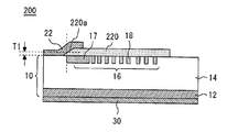
- FIG. 3 is a cross-sectional view of the Schottky barrier diode 200 according to the second embodiment.
- the shape of the insulating film 20 of the Schottky barrier diode 200 is different from that of the Schottky barrier diode 100.
- the inner end of the insulating film 20 has a right-angled shape.
- the side provided inside the semiconductor substrate 10 has a tapered shape.
- the insulating film 20 has a tapered portion 220a that becomes thinner toward the end portion.
- the capacitance component can be adjusted by the angle of the end portion of the insulating film 20. Further, the capacitance can be adjusted without changing the maximum value of the thickness of the insulating film 20.
- the thickness T1 of the insulating film 20 is, for example, 1.0 ⁇ m or more just above the side of the end of the inner guard ring 17 provided inside the semiconductor substrate 10. Thereby, as in the first embodiment, it is possible to prevent the inversion layer from being formed.
- the tapered portion 220a is provided directly above the inner end portion of the inner guard ring 17. Thereby, the forward voltage Vpn can be adjusted at a position where the current is likely to be concentrated. Not limited to this, the tapered portion 220a may be provided at a portion sandwiched between the anode electrode 22 and the guard ring 16. As a result, the effect of adjusting the volume component can be obtained.
- FIG. 4 is a cross-sectional view of the Schottky barrier diode 300 according to the third embodiment.
- the structure of the cathode electrode 330 of the Schottky barrier diode 300 is different from that of the Schottky barrier diode 100.
- the cathode electrode 330 is formed with an opening 332 that exposes the semiconductor substrate 10 directly below the inner guard ring 17.
- a part of the cathode electrode 330 is removed just below the inner guard ring 17. Therefore, the cathode electrode 330 is separated into a cell region 10a side and a terminal region 10b side. As a result, the path of the current from the inner guard ring 17 becomes long, and the forward voltage Vpn can be increased. Further, by reducing the area of the cathode electrode 330, the forward voltage Vpn can be increased. Therefore, the current concentration in the guard ring 16 can be suppressed.
- the opening 332 exposes the semiconductor substrate 10 within a certain range L3 from directly below the inner guard ring 17.
- the forward voltage Vpn can be adjusted by adjusting the distance L3.
- the distance L3 is, for example, the thickness of the drift layer.
- the angle formed by the virtual line connecting the end of the inner guard ring 17 and the end of the cathode electrode 330 and the perpendicular line perpendicular to the back surface of the semiconductor substrate 10 is defined as ⁇ 1.
- the forward voltage Vpn can be adjusted by changing ⁇ 1. The larger ⁇ 1, the higher the forward voltage Vpn.
- the strength at the time of die bonding can be improved by the portion of the cathode electrode 330 separated by the opening 332 on the terminal region 10b side. Further, the portion of the separated cathode electrode 330 on the terminal region 10b side may be omitted.
- the area of the opening 332 is larger than the area of the inner guard ring 17.
- the cathode electrode 330 may have an opening 332 formed in at least a part of the portion directly below the inner guard ring 17.
- FIG. 5 is a cross-sectional view of the Schottky barrier diode 400 according to the fourth embodiment.
- the Schottky barrier diode 400 differs from the Schottky barrier diode 100 in that it includes a second p-type semiconductor layer 411.
- the second p-type semiconductor layer 411 is provided directly below the inner guard ring 17 in the semiconductor substrate 10.
- the second p-type semiconductor layer 411 is provided on the back surface side of the semiconductor substrate 10.
- the conduction region on the cathode side is limited by the second p-type semiconductor layer 411. That is, the second p-type semiconductor layer 411 lengthens the path of the current to the cathode side. Therefore, the forward voltage Vpn can be further increased. Therefore, the current concentration in the guard ring 16 can be suppressed.
- the second p-type semiconductor layer 411 is provided from directly below the inner guard ring 17 to a certain range L4.
- the forward voltage Vpn can be adjusted by adjusting the distance L4.
- the angle formed by the virtual line connecting the end of the inner guard ring 17 and the end of the second p-type semiconductor layer 411 and the perpendicular line perpendicular to the back surface of the semiconductor substrate 10 is defined as ⁇ 2.
- the forward voltage Vpn can be adjusted by changing ⁇ 2. The larger ⁇ 2, the higher the forward voltage Vpn.
- the area of the second p-type semiconductor layer 411 is larger than the area of the inner guard ring 17.
- the second p-type semiconductor layer 411 may be provided at least in a part of the portion directly below the inner guard ring 17 of the semiconductor substrate 10.
- the second p-type semiconductor layer 411 may be provided only directly below the inner guard ring 17 in the semiconductor substrate 10.
- the second p-type semiconductor layer 411 is provided on the n + type semiconductor layer 12 and is exposed on the back surface of the semiconductor substrate 10.
- the second p-type semiconductor layer 411 may be provided at a position directly below the inner guard ring 17 and deeper than the back surface of the semiconductor substrate 10. That is, the second p-type semiconductor layer 411 does not have to be exposed on the back surface of the semiconductor substrate 10. Also in this case, the path of the current from the inner guard ring 17 to the cathode side can be lengthened, and the forward voltage Vpn can be increased.
- the second p-type semiconductor layer 411 may extend to the end of the terminal region 10b.
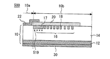
- FIG. 6 is a cross-sectional view of the Schottky barrier diode 500 according to the fifth embodiment.
- the Schottky barrier diode 500 differs from the Schottky barrier diode 100 in that it includes a crystal defect layer 519.
- the crystal defect layer 519 is provided directly below the inner guard ring 17 of the semiconductor substrate 10.
- the crystal defect layer 519 is formed by ion irradiation, electron beam irradiation, or the like.
- the forward voltage Vpn can be increased by increasing the speed of the pn junction. Therefore, the current concentration in the guard ring 16 can be suppressed.
- the crystal defect layer 519 is provided only directly below the inner guard ring 17 among the plurality of guard rings 16. As a result, it is possible to suppress a decrease in the withstand voltage of the terminal region 10b. Not limited to this, the crystal defect layer 519 may be provided directly below the outer guard ring 18.
- FIG. 7 is a cross-sectional view of the Schottky barrier diode 600 according to the sixth embodiment.
- the Schottky barrier diode 600 is different from the Schottky barrier diode 100 in that it includes a first p-type semiconductor layer 615.
- the first p-type semiconductor layer 615 is provided on the upper surface side of the semiconductor substrate 10 inside the inner guard ring 17 and in contact with the inner guard ring 17.
- the concentration of the first p-type semiconductor layer 615 is lower than that of the inner guard ring 17.
- the inner guard ring 17 and the first p-type semiconductor layer 615 are electrically connected and have the same potential.
- the insulating film 20 covers the entire upper surface of the inner guard ring 17.
- the first p-type semiconductor layer 615 is exposed from the insulating film 20.
- the end of the first p-type semiconductor layer 615 provided inside the semiconductor substrate 10 is exposed from the insulating film 20. More than half of the upper surface of the first p-type semiconductor layer 615 is exposed from the insulating film 20.
- the portion of the upper surface of the first p-type semiconductor layer 615 exposed from the insulating film 20 comes into direct contact with the anode electrode 22.
- the inner guard ring 17 and the anode electrode 22 are separated by a first p-type semiconductor layer 615.
- the first p-type semiconductor layer 615 has a higher resistance than the inner guard ring 17.
- the contact resistance between the first p-type semiconductor layer 615 and the anode electrode 22 having an impurity concentration lower than that of the inner guard ring 17 is higher than the contact resistance between the inner guard ring 17 and the anode electrode 22. Therefore, the current concentration in the guard ring 16 can be suppressed as in the first embodiment.
- the first p-type semiconductor layer 615 is provided inside the inner guard ring 17.
- the first p-type semiconductor layer 615 may be provided so as to separate the anode electrode 22 and the inner guard ring 17.
- the inner guard ring 17 may be included in the first p-type semiconductor layer 615.
- the high resistance layer that separates the inner guard ring 17 and the anode electrode 22 is not limited to the first p-type semiconductor layer 615.
- the inner guard ring 17 and the anode electrode 22 may be separated by a layer having a higher resistance than the inner guard ring 17.
- the inner guard ring 17 and the anode electrode 22 may be separated by a layer in which the contact resistance between the inner guard ring 17 and the anode electrode 22 is higher than the contact resistance between the inner guard ring 17 and the anode electrode 22.
- the anode electrode 22 is provided at an end portion directly above the inner guard ring 17. Not limited to this, the anode electrode 22 may extend above the outer guard ring 18.
- FIG. 8 is a cross-sectional view of the Schottky barrier diode 700 according to the seventh embodiment.
- the present embodiment differs from the Schottky barrier diode 100 in that the insulating film 20 is arranged and the resistor 724 is provided.
- the insulating film 20 covers a plurality of guard rings 16 except for a part of the inner guard ring 17.
- the inner guard ring 17 has an exposed portion exposed from the insulating film 20 on the side of the end portion provided inside the semiconductor substrate 10.
- the resistor 724 covers the exposed portion.
- the resistor 724 is, for example, a polysilicon resistor.
- the resistor 724 is provided inside the insulating film 20 on the upper surface of the semiconductor substrate 10.
- the resistor 724 is adjacent to the insulating film 20.
- the resistor 724 has a higher resistance than the inner guard ring 17.
- the anode electrode 22 rides on the resistor 724 and the insulating film 20.
- the resistor 724 corresponds to the high resistance layer that separates the inner guard ring 17 and the anode electrode 22.
- the resistance component of the resistor 724 can suppress the current concentration in the guard ring 16 as in the sixth embodiment.
- the resistor 724 may be provided between the anode electrode 22 and the inner guard ring 17.
- the resistor 724 may be provided in the semiconductor substrate 10.
- both the first p-type semiconductor layer 615 described in the sixth embodiment and the resistor 724 may be provided. Thereby, the forward voltage Vpn can be further increased.
Abstract
This Schottky barrier diode is provided with an n-type semiconductor substrate, at least one p-type guard ring provided on the top surface side of the semiconductor substrate, an anode electrode provided on the top surface of the semiconductor substrate, a cathode electrode provided on the back surface of the semiconductor substrate, and an insulation film provided on the innermost inside guard ring of the at least one guard ring, wherein the anode electrode rides up on the insulation film and the edge thereof is provided directly above the inside guard ring; the anode electrode and inside guard ring are provided separated from each other, and the insulation film is at least 1.0μm thick.
Description
本開示は、ショットキーバリアダイオードに関する。
This disclosure relates to Schottky barrier diodes.
特許文献1には、一導電型の半導体基体の表面に逆導電型の半導体層より成るガードリングを形成したショットキーバリアダイオードが開示されている。
Patent Document 1 discloses a Schottky barrier diode in which a guard ring made of a reverse conductive semiconductor layer is formed on the surface of a monoconductive semiconductor substrate.
特許文献1に示されるショットキーバリアダイオードでは、順方向電流が増加すると、ショットキー部の順方向電圧降下よりもガードリングと半導体基板の間に形成されるpn接合の順方向電圧降下の方が低くなる可能性がある。これにより、電流集中により終端領域が破壊するおそれがある。
In the Schottky barrier diode shown in Patent Document 1, when the forward current increases, the forward voltage drop of the pn junction formed between the guard ring and the semiconductor substrate becomes larger than the forward voltage drop of the Schottky portion. It can be low. As a result, the end region may be destroyed due to current concentration.
本開示は、上述の課題を解決するためになされたもので、その目的は、ガードリングでの電流集中を抑制できるショットキーバリアダイオードを得ることである。
The present disclosure has been made to solve the above-mentioned problems, and an object thereof is to obtain a Schottky barrier diode capable of suppressing current concentration in a guard ring.
本開示に係るショットキーバリアダイオードは、n型の半導体基板と、該半導体基板の上面側に設けられた少なくとも1つのp型のガードリングと、該半導体基板の上面に設けられたアノード電極と、該半導体基板の裏面に設けられたカソード電極と、該少なくとも1つのガードリングのうち最も内側の内側ガードリングの上に設けられた絶縁膜と、を備え、該アノード電極は該絶縁膜の上に乗り上げ、端部が該内側ガードリングの直上に設けられ、該アノード電極と該内側ガードリングは離れて設けられ、該絶縁膜の厚さは1.0μm以上である。
The Schottky barrier diode according to the present disclosure includes an n-type semiconductor substrate, at least one p-type guard ring provided on the upper surface side of the semiconductor substrate, and an anode electrode provided on the upper surface side of the semiconductor substrate. A cathode electrode provided on the back surface of the semiconductor substrate and an insulating film provided on the innermost inner guard ring of the at least one guard ring are provided, and the anode electrode is provided on the insulating film. The riding and end portions are provided directly above the inner guard ring, the anode electrode and the inner guard ring are provided apart from each other, and the thickness of the insulating film is 1.0 μm or more.
本開示に係るショットキーバリアダイオードは、n型の半導体基板と、該半導体基板の上面側に設けられたp型の複数のガードリングと、該半導体基板の上面に設けられたアノード電極と、該半導体基板の裏面に設けられたカソード電極と、該複数のガードリングのうち最も内側の内側ガードリングの上に設けられた絶縁膜と、を備え、該アノード電極は該絶縁膜の上に乗り上げ、端部が該内側ガードリングの直上に設けられ、該アノード電極と該内側ガードリングは離れて設けられる。
The Schottky barrier diode according to the present disclosure includes an n-type semiconductor substrate, a plurality of p-type guard rings provided on the upper surface side of the semiconductor substrate, an anode electrode provided on the upper surface of the semiconductor substrate, and the like. A cathode electrode provided on the back surface of the semiconductor substrate and an insulating film provided on the innermost inner guard ring among the plurality of guard rings are provided, and the anode electrode rides on the insulating film. The end is provided directly above the inner guard ring, and the anode electrode and the inner guard ring are provided separately.
本開示に係るショットキーバリアダイオードは、n型の半導体基板と、該半導体基板の上面側に設けられた少なくとも1つのp型のガードリングと、該少なくとも1つのガードリングのうち最も内側の内側ガードリングの上に設けられた絶縁膜と、該半導体基板の上面に設けられ、該絶縁膜の上に乗り上げたアノード電極と、該半導体基板の裏面に設けられたカソード電極と、該内側ガードリングよりも高抵抗であり、該内側ガードリングと該アノード電極とを隔てる高抵抗層と、を備える。
The Schottky barrier diode according to the present disclosure includes an n-type semiconductor substrate, at least one p-type guard ring provided on the upper surface side of the semiconductor substrate, and the innermost inner guard of the at least one guard ring. From the insulating film provided on the ring, the anode electrode provided on the upper surface of the semiconductor substrate and riding on the insulating film, the cathode electrode provided on the back surface of the semiconductor substrate, and the inner guard ring. Also has high resistance, and includes a high resistance layer that separates the inner guard ring and the anode electrode.
本開示に係るショットキーバリアダイオードでは、絶縁膜の持つ容量成分を介してアノード電極とガードリングとが接続される。従って、ガードリングでの電流集中を抑制できる。
In the Schottky barrier diode according to the present disclosure, the anode electrode and the guard ring are connected via the capacitive component of the insulating film. Therefore, the current concentration in the guard ring can be suppressed.
各実施の形態に係るショットキーバリアダイオードについて図面を参照して説明する。同じ又は対応する構成要素には同じ符号を付し、説明の繰り返しを省略する場合がある。
The Schottky barrier diode according to each embodiment will be described with reference to the drawings. The same or corresponding components may be designated by the same reference numerals and the description may be omitted.
実施の形態1.
図1は、実施の形態1に係るショットキーバリアダイオード100の断面図である。ショットキーバリアダイオード100は、半導体基板10を備える。半導体基板10は例えばシリコンから形成される。半導体基板10は、n+型半導体層12とn+型半導体層12の上に設けられたn型半導体層14を備える。 Embodiment 1.
FIG. 1 is a cross-sectional view of theSchottky barrier diode 100 according to the first embodiment. The Schottky barrier diode 100 includes a semiconductor substrate 10. The semiconductor substrate 10 is formed of, for example, silicon. The semiconductor substrate 10 includes an n + type semiconductor layer 12 and an n-type semiconductor layer 14 provided on the n + type semiconductor layer 12.
図1は、実施の形態1に係るショットキーバリアダイオード100の断面図である。ショットキーバリアダイオード100は、半導体基板10を備える。半導体基板10は例えばシリコンから形成される。半導体基板10は、n+型半導体層12とn+型半導体層12の上に設けられたn型半導体層14を備える。 Embodiment 1.
FIG. 1 is a cross-sectional view of the
半導体基板10の上面側には、p型の複数のガードリング16が設けられる。複数のガードリング16のうち最も内側のガードリング16を内側ガードリング17とする。また、複数のガードリング16のうち、内側ガードリング17以外のガードリング16を外側ガードリング18とする。
A plurality of p-type guard rings 16 are provided on the upper surface side of the semiconductor substrate 10. The innermost guard ring 16 among the plurality of guard rings 16 is referred to as an inner guard ring 17. Further, among the plurality of guard rings 16, the guard ring 16 other than the inner guard ring 17 is referred to as the outer guard ring 18.
半導体基板10は、ショットキーバリアダイオード100の主電流が流れるセル領域10aと、セル領域10aを囲む終端領域10bを有する。本実施の形態では、内側ガードリング17の内側の端部が終端領域10bとセル領域10aの境界である。ここで、内側は半導体基板10において終端領域10bに対してセル領域10aが設けられる側である。ガードリング16は、セル領域10aを囲むように形成されている。
The semiconductor substrate 10 has a cell region 10a through which the main current of the Schottky barrier diode 100 flows, and a terminal region 10b surrounding the cell region 10a. In the present embodiment, the inner end of the inner guard ring 17 is the boundary between the terminal region 10b and the cell region 10a. Here, the inside is the side of the semiconductor substrate 10 where the cell region 10a is provided with respect to the termination region 10b. The guard ring 16 is formed so as to surround the cell region 10a.
半導体基板10の上面にはアノード電極22が設けられる。アノード電極22はセル領域10aにおいてn型半導体層14と電気的に接続される。アノード電極22はショットキーバリア電極である。半導体基板10の裏面には、カソード電極30が設けられる。カソード電極30は、n+型半導体層12と電気的に接続される。
An anode electrode 22 is provided on the upper surface of the semiconductor substrate 10. The anode electrode 22 is electrically connected to the n-type semiconductor layer 14 in the cell region 10a. The anode electrode 22 is a Schottky barrier electrode. A cathode electrode 30 is provided on the back surface of the semiconductor substrate 10. The cathode electrode 30 is electrically connected to the n + type semiconductor layer 12.
ガードリング16の上には絶縁膜20が設けられる。絶縁膜20の厚さT1は例えば1.0μm以上である。絶縁膜20は、複数のガードリング16の上面を全て覆う。
An insulating film 20 is provided on the guard ring 16. The thickness T1 of the insulating film 20 is, for example, 1.0 μm or more. The insulating film 20 covers all the upper surfaces of the plurality of guard rings 16.
アノード電極22は絶縁膜20の上に乗り上げる。アノード電極22の端部は、内側ガードリング17の直上に設けられる。絶縁膜20はアノード電極22と内側ガードリング17とが接触しないよう設けられている。このように、アノード電極22と内側ガードリング17は離れて設けられる。
The anode electrode 22 rides on the insulating film 20. The end of the anode electrode 22 is provided directly above the inner guard ring 17. The insulating film 20 is provided so that the anode electrode 22 and the inner guard ring 17 do not come into contact with each other. In this way, the anode electrode 22 and the inner guard ring 17 are provided apart from each other.
一般にショットキーバリアダイオードにおいて、p型ガードリング領域の最内周の部分にショットキーバリア電極が接することで、ガードリングに電位を伝えて耐圧を保持することがある。ここで、順方向電流が増加すると、ショットキー部の順方向電圧VFよりもガードリングと半導体基板の間に形成されるpn接合の順方向電圧Vpnの方が低くなる可能性がある。このため、特に還流中等にガードリングに電流が集中するおそれがある。
Generally, in a Schottky barrier diode, when the Schottky barrier electrode comes into contact with the innermost part of the p-type guard ring region, the potential may be transmitted to the guard ring to maintain the withstand voltage. Here, when the forward current increases, the forward voltage Vpn of the pn junction formed between the guard ring and the semiconductor substrate may be lower than the forward voltage VF of the Schottky portion. Therefore, the current may be concentrated on the guard ring, especially during reflux.
これに対し本実施の形態では、アノード電極22とガードリング16とが絶縁膜20を介して接続される。このため、絶縁膜20の持つ容量成分により、アノード電極22、絶縁膜20、内側ガードリング17、n型半導体層14を繋ぐ経路の順方向電圧Vpnを調整できる。このため、アノード電極22、n型半導体層14間の順方向電圧VFよりも順方向電圧Vpnが低くならないように調整できる。従って、ガードリング16での電流集中を抑制できる。これにより、ショットキーバリアダイオード100の熱暴走による破壊を回避できる。
On the other hand, in the present embodiment, the anode electrode 22 and the guard ring 16 are connected via the insulating film 20. Therefore, the forward voltage Vpn of the path connecting the anode electrode 22, the insulating film 20, the inner guard ring 17, and the n-type semiconductor layer 14 can be adjusted by the capacitance component of the insulating film 20. Therefore, the forward voltage Vpn can be adjusted so as not to be lower than the forward voltage VF between the anode electrode 22 and the n-type semiconductor layer 14. Therefore, the current concentration in the guard ring 16 can be suppressed. As a result, it is possible to avoid destruction of the Schottky barrier diode 100 due to thermal runaway.
絶縁膜20の容量成分は、予め定められた電流の範囲内で、Vpn>VFとなるように調整されても良い。予め定められた電流の範囲は、例えばショットキーバリアダイオード100の駆動時に流れる電流の範囲である。
The capacitance component of the insulating film 20 may be adjusted so that Vpn> VF within a predetermined current range. The predetermined current range is, for example, the range of the current that flows when the Schottky barrier diode 100 is driven.
また、アノード電極22を、絶縁膜20を介してガードリング16の上にオーバーラップするように形成することで、セル領域10aと終端領域10bの境界付近での電位を安定化させることができる。
Further, by forming the anode electrode 22 so as to overlap the guard ring 16 via the insulating film 20, the potential near the boundary between the cell region 10a and the terminal region 10b can be stabilized.
また、電流集中はセル領域10aと終端領域10bの境界付近で起こりやすい。このため、複数のガードリング16のうち、特に内側ガードリング17とアノード電極22とが接触しないことで、電流集中を効果的に抑制できる。このため、複数のガードリング16のうち少なくとも内側ガードリング17がアノード電極22と離れていればよい。つまり、全てのガードリング16がアノード電極22と離れていても良く、外側ガードリング18がアノード電極22と接触していても良い。
In addition, current concentration tends to occur near the boundary between the cell region 10a and the terminal region 10b. Therefore, among the plurality of guard rings 16, the inner guard ring 17 and the anode electrode 22 do not come into contact with each other, so that current concentration can be effectively suppressed. Therefore, at least the inner guard ring 17 of the plurality of guard rings 16 may be separated from the anode electrode 22. That is, all the guard rings 16 may be separated from the anode electrode 22, and the outer guard ring 18 may be in contact with the anode electrode 22.
また、絶縁膜20は少なくとも内側ガードリング17の上に設けられていればよい。絶縁膜20は内側ガードリング17の上面を全て覆い、外側ガードリング18を露出させても良い。また、内側ガードリング17とアノード電極22とが接触しなければ、内側ガードリング17の一部が絶縁膜20から露出しても良い。
Further, the insulating film 20 may be provided at least on the inner guard ring 17. The insulating film 20 may cover the entire upper surface of the inner guard ring 17 to expose the outer guard ring 18. Further, if the inner guard ring 17 and the anode electrode 22 do not come into contact with each other, a part of the inner guard ring 17 may be exposed from the insulating film 20.
また、本実施の形態の絶縁膜20の厚さT1は1μm以上である。本実施の形態の比較例として、絶縁膜20の下部にp型チャネルの反転層ができるように、例えば0.5μm以下の薄い絶縁膜を形成することを考える。このとき、反転層はガードリングよりも浅い領域にしか形成されないことが考えられる。このため、空乏層が終端領域側へ伸びにくく、曲率が大きくなる可能性がある。従って、ショットキーバリアダイオードの耐圧が低下するおそれがある。
Further, the thickness T1 of the insulating film 20 of the present embodiment is 1 μm or more. As a comparative example of this embodiment, it is considered to form a thin insulating film of, for example, 0.5 μm or less so that an inversion layer of a p-type channel is formed under the insulating film 20. At this time, it is considered that the inversion layer is formed only in a region shallower than the guard ring. Therefore, the depletion layer is difficult to extend toward the terminal region side, and the curvature may increase. Therefore, the withstand voltage of the Schottky barrier diode may decrease.
これに対し、本実施の形態では内側ガードリング17近傍に反転層が形成されないように絶縁膜20の厚さT1は1.0μm以上に設定される。これにより、絶縁膜20の下部がチャネル反転することを防止できる。また、絶縁膜20により静電容量を確保し、アノード電極22とガードリング16の電位を固定できる。絶縁膜20は、TEOS(TetraEthOxySilane)等の堆積酸化膜で形成されても良い。
On the other hand, in the present embodiment, the thickness T1 of the insulating film 20 is set to 1.0 μm or more so that the inversion layer is not formed in the vicinity of the inner guard ring 17. As a result, it is possible to prevent the lower portion of the insulating film 20 from being channel inverted. Further, the capacitance can be secured by the insulating film 20, and the potentials of the anode electrode 22 and the guard ring 16 can be fixed. The insulating film 20 may be formed of a deposited oxide film such as TEOS (TetraEthOxySilane).
絶縁膜20の厚さT1は電流集中を抑制できれば1.0μm未満でも良い。また、本実施の形態では複数のガードリング16が設けられるものとした。これに限らず、ガードリング16は少なくとも1つ設けられれば良い。
The thickness T1 of the insulating film 20 may be less than 1.0 μm as long as the current concentration can be suppressed. Further, in the present embodiment, a plurality of guard rings 16 are provided. Not limited to this, at least one guard ring 16 may be provided.
また、アノード電極22を外側ガードリング18の上まで伸ばすと、電界分布が変化して耐圧が低下する場合がある。また、アノード電極22と他の金属部との沿面距離が短くなり、放電しやすくなる可能性がある。これに対し、本実施の形態では、アノード電極22の端部は、内側ガードリング17の直上に設けられる。このため、外側ガードリング18は絶縁膜20を介してアノード電極22と容量結合しない。従って、耐圧の低下を抑制できる。また、沿面距離を確保できる。
Further, when the anode electrode 22 is extended above the outer guard ring 18, the electric field distribution may change and the withstand voltage may decrease. Further, the creepage distance between the anode electrode 22 and the other metal portion is shortened, which may facilitate discharge. On the other hand, in the present embodiment, the end portion of the anode electrode 22 is provided directly above the inner guard ring 17. Therefore, the outer guard ring 18 does not capacitively couple with the anode electrode 22 via the insulating film 20. Therefore, it is possible to suppress a decrease in withstand voltage. In addition, the creepage distance can be secured.
また、本実施の形態の構成によれば、内側ガードリング17とアノード電極22との重畳面積によって容量成分を調整できる。
Further, according to the configuration of the present embodiment, the capacitance component can be adjusted by the overlapping area of the inner guard ring 17 and the anode electrode 22.
図2は、実施の形態1に係るショットキーバリアダイオード100の寸法を説明する図である。内側ガードリング17の幅L2は、アノード電極22のうち絶縁膜20に乗り上げた部分の幅L1以上であると良い。例えば、L1=20μmであり、L2=50μmである。これにより、製造バラツキによりアノード電極22と内側ガードリング17の位置関係にズレが生じた場合であっても、確実にアノード電極22の端部を内側ガードリング17の直上に配置できる。従って、アノード電極22と内側ガードリング17を確実に容量結合させることが可能になる。また、アノード電極22と外側ガードリング18が容量結合することを防止できる。
FIG. 2 is a diagram illustrating the dimensions of the Schottky barrier diode 100 according to the first embodiment. The width L2 of the inner guard ring 17 is preferably equal to or greater than the width L1 of the portion of the anode electrode 22 that rides on the insulating film 20. For example, L1 = 20 μm and L2 = 50 μm. As a result, even if the positional relationship between the anode electrode 22 and the inner guard ring 17 is displaced due to manufacturing variations, the end portion of the anode electrode 22 can be reliably arranged directly above the inner guard ring 17. Therefore, the anode electrode 22 and the inner guard ring 17 can be reliably capacitively coupled. Further, it is possible to prevent the anode electrode 22 and the outer guard ring 18 from being capacitively coupled.
半導体基板10は、シリコンよりバンドギャップの大きいワイドバンドギャップ半導体から形成されても良い。ワイドバンドギャップ半導体は、例えば炭化珪素、酸化ガリウム、窒化ガリウム系材料またはダイヤモンドである。これにより、順方向電圧Vpnを高くすることができる。特に、炭化珪素よりバンドギャップが大きい酸化ガリウム等を使用することで、セル領域10aでの電流負担を増やしてガードリング16での電流集中を抑制できる。
The semiconductor substrate 10 may be formed of a wide bandgap semiconductor having a bandgap larger than that of silicon. Wide bandgap semiconductors are, for example, silicon carbide, gallium oxide, gallium nitride based materials or diamond. Thereby, the forward voltage Vpn can be increased. In particular, by using gallium oxide or the like having a bandgap larger than that of silicon carbide, the current load in the cell region 10a can be increased and the current concentration in the guard ring 16 can be suppressed.
これらの変形は以下の実施の形態に係るショットキーバリアダイオードについて適宜応用することができる。なお、以下の実施の形態に係るショットキーバリアダイオードについては実施の形態1との共通点が多いので、実施の形態1との相違点を中心に説明する。
These modifications can be appropriately applied to the Schottky barrier diode according to the following embodiment. Since the Schottky barrier diode according to the following embodiment has much in common with the first embodiment, the differences from the first embodiment will be mainly described.
実施の形態2.
図3は、実施の形態2に係るショットキーバリアダイオード200の断面図である。ショットキーバリアダイオード200は絶縁膜20の形状がショットキーバリアダイオード100と異なる。実施の形態1において、絶縁膜20の内側の端部は直角形状であった。これに対し、本実施の形態に係る絶縁膜20の端部のうち半導体基板10の内側に設けられた側は、テーパー状である。 Embodiment 2.
FIG. 3 is a cross-sectional view of theSchottky barrier diode 200 according to the second embodiment. The shape of the insulating film 20 of the Schottky barrier diode 200 is different from that of the Schottky barrier diode 100. In the first embodiment, the inner end of the insulating film 20 has a right-angled shape. On the other hand, of the end portions of the insulating film 20 according to the present embodiment, the side provided inside the semiconductor substrate 10 has a tapered shape.
図3は、実施の形態2に係るショットキーバリアダイオード200の断面図である。ショットキーバリアダイオード200は絶縁膜20の形状がショットキーバリアダイオード100と異なる。実施の形態1において、絶縁膜20の内側の端部は直角形状であった。これに対し、本実施の形態に係る絶縁膜20の端部のうち半導体基板10の内側に設けられた側は、テーパー状である。 Embodiment 2.
FIG. 3 is a cross-sectional view of the
絶縁膜20は端部に向かって薄くなるテーパー部220aを有する。本実施の形態では、絶縁膜20の端部の角度により、容量成分を調整できる。また、絶縁膜20の厚さの最大値を変えずに、容量を調整できる。
The insulating film 20 has a tapered portion 220a that becomes thinner toward the end portion. In the present embodiment, the capacitance component can be adjusted by the angle of the end portion of the insulating film 20. Further, the capacitance can be adjusted without changing the maximum value of the thickness of the insulating film 20.
絶縁膜20の厚さT1は、例えば内側ガードリング17の端部のうち半導体基板10の内側に設けられた側の直上で1.0μm以上である。これにより、実施の形態1と同様に、反転層が形成されることを防止できる。
The thickness T1 of the insulating film 20 is, for example, 1.0 μm or more just above the side of the end of the inner guard ring 17 provided inside the semiconductor substrate 10. Thereby, as in the first embodiment, it is possible to prevent the inversion layer from being formed.
また、テーパー部220aは、内側ガードリング17の内側の端部の直上に設けられる。これにより、電流が集中しやすい位置で順方向電圧Vpnを調整できる。これに限らず、テーパー部220aは、アノード電極22とガードリング16で挟まれた部分に設けられれば良い。これにより、容量成分の調整の効果が得られる。
Further, the tapered portion 220a is provided directly above the inner end portion of the inner guard ring 17. Thereby, the forward voltage Vpn can be adjusted at a position where the current is likely to be concentrated. Not limited to this, the tapered portion 220a may be provided at a portion sandwiched between the anode electrode 22 and the guard ring 16. As a result, the effect of adjusting the volume component can be obtained.
実施の形態3.
図4は、実施の形態3に係るショットキーバリアダイオード300の断面図である。ショットキーバリアダイオード300は、カソード電極330の構造がショットキーバリアダイオード100と異なる。カソード電極330には、内側ガードリング17の直下に半導体基板10を露出させる開口部332が形成される。 Embodiment 3.
FIG. 4 is a cross-sectional view of theSchottky barrier diode 300 according to the third embodiment. The structure of the cathode electrode 330 of the Schottky barrier diode 300 is different from that of the Schottky barrier diode 100. The cathode electrode 330 is formed with an opening 332 that exposes the semiconductor substrate 10 directly below the inner guard ring 17.
図4は、実施の形態3に係るショットキーバリアダイオード300の断面図である。ショットキーバリアダイオード300は、カソード電極330の構造がショットキーバリアダイオード100と異なる。カソード電極330には、内側ガードリング17の直下に半導体基板10を露出させる開口部332が形成される。 Embodiment 3.
FIG. 4 is a cross-sectional view of the
カソード電極330は、内側ガードリング17の直下において一部が取り除かれる。このため、カソード電極330はセル領域10a側と終端領域10b側とに分離される。これにより、内側ガードリング17からの電流の経路が長くなり、順方向電圧Vpnを高くすることができる。また、カソード電極330の面積が小さくなることで、順方向電圧Vpnを高くすることができる。従って、ガードリング16での電流集中を抑制できる。
A part of the cathode electrode 330 is removed just below the inner guard ring 17. Therefore, the cathode electrode 330 is separated into a cell region 10a side and a terminal region 10b side. As a result, the path of the current from the inner guard ring 17 becomes long, and the forward voltage Vpn can be increased. Further, by reducing the area of the cathode electrode 330, the forward voltage Vpn can be increased. Therefore, the current concentration in the guard ring 16 can be suppressed.
また、本実施の形態では開口部332は、内側ガードリング17の直下から一定の範囲L3で半導体基板10を露出させる。距離L3の調整により順方向電圧Vpnを調整できる。距離L3は例えばドリフト層厚である。また、内側ガードリング17の端部とカソード電極330の端部を繋ぐ仮想線と、半導体基板10の裏面に垂直な垂線とが成す角をθ1とする。θ1の変更により順方向電圧Vpnを調整できる。θ1が大きいほど順方向電圧Vpnは高くなる。
Further, in the present embodiment, the opening 332 exposes the semiconductor substrate 10 within a certain range L3 from directly below the inner guard ring 17. The forward voltage Vpn can be adjusted by adjusting the distance L3. The distance L3 is, for example, the thickness of the drift layer. Further, the angle formed by the virtual line connecting the end of the inner guard ring 17 and the end of the cathode electrode 330 and the perpendicular line perpendicular to the back surface of the semiconductor substrate 10 is defined as θ1. The forward voltage Vpn can be adjusted by changing θ1. The larger θ1, the higher the forward voltage Vpn.
開口部332で分離されたカソード電極330のうち終端領域10b側の部分により、ダイボンド時の強度を向上できる。また、分離されたカソード電極330のうち終端領域10b側の部分は省略されても良い。
The strength at the time of die bonding can be improved by the portion of the cathode electrode 330 separated by the opening 332 on the terminal region 10b side. Further, the portion of the separated cathode electrode 330 on the terminal region 10b side may be omitted.
図4の例では、開口部332の面積は内側ガードリング17の面積よりも大きい。これに限らず、カソード電極330には、内側ガードリング17の直下の部分のうち少なくとも一部に開口部332が形成されればよい。
In the example of FIG. 4, the area of the opening 332 is larger than the area of the inner guard ring 17. Not limited to this, the cathode electrode 330 may have an opening 332 formed in at least a part of the portion directly below the inner guard ring 17.
実施の形態4.
図5は、実施の形態4に係るショットキーバリアダイオード400の断面図である。ショットキーバリアダイオード400は、第2p型半導体層411を備える点がショットキーバリアダイオード100と異なる。第2p型半導体層411は、半導体基板10のうち、内側ガードリング17の直下に設けられる。第2p型半導体層411は、半導体基板10の裏面側に設けられる。 Embodiment 4.
FIG. 5 is a cross-sectional view of theSchottky barrier diode 400 according to the fourth embodiment. The Schottky barrier diode 400 differs from the Schottky barrier diode 100 in that it includes a second p-type semiconductor layer 411. The second p-type semiconductor layer 411 is provided directly below the inner guard ring 17 in the semiconductor substrate 10. The second p-type semiconductor layer 411 is provided on the back surface side of the semiconductor substrate 10.
図5は、実施の形態4に係るショットキーバリアダイオード400の断面図である。ショットキーバリアダイオード400は、第2p型半導体層411を備える点がショットキーバリアダイオード100と異なる。第2p型半導体層411は、半導体基板10のうち、内側ガードリング17の直下に設けられる。第2p型半導体層411は、半導体基板10の裏面側に設けられる。 Embodiment 4.
FIG. 5 is a cross-sectional view of the
第2p型半導体層411によって、カソード側の導通領域が制限される。つまり、第2p型半導体層411によって、カソード側への電流の経路が長くなる。このため、順方向電圧Vpnをさらに高くすることができる。従って、ガードリング16での電流集中を抑制できる。
The conduction region on the cathode side is limited by the second p-type semiconductor layer 411. That is, the second p-type semiconductor layer 411 lengthens the path of the current to the cathode side. Therefore, the forward voltage Vpn can be further increased. Therefore, the current concentration in the guard ring 16 can be suppressed.
第2p型半導体層411は、内側ガードリング17の直下から一定の範囲L4まで設けられる。距離L4の調整により順方向電圧Vpnを調整できる。また、内側ガードリング17の端部と第2p型半導体層411の端部を繋ぐ仮想線と、半導体基板10の裏面に垂直な垂線とが成す角をθ2とする。θ2の変更により順方向電圧Vpnを調整できる。θ2が大きいほど順方向電圧Vpnは高くなる。
The second p-type semiconductor layer 411 is provided from directly below the inner guard ring 17 to a certain range L4. The forward voltage Vpn can be adjusted by adjusting the distance L4. Further, the angle formed by the virtual line connecting the end of the inner guard ring 17 and the end of the second p-type semiconductor layer 411 and the perpendicular line perpendicular to the back surface of the semiconductor substrate 10 is defined as θ2. The forward voltage Vpn can be adjusted by changing θ2. The larger θ2, the higher the forward voltage Vpn.
図5の例では、第2p型半導体層411の面積は内側ガードリング17の面積よりも大きい。これに限らず、半導体基板10の内側ガードリング17の直下の部分のうち、少なくとも一部に第2p型半導体層411が設けられれば良い。例えば、第2p型半導体層411は、半導体基板10のうち、内側ガードリング17の直下のみに設けられても良い。セル領域10aにおける第2p型半導体層411の面積を抑制することで、ショットキーバリアダイオード400の電気的特性への第2p型半導体層411の影響を抑制できる。
In the example of FIG. 5, the area of the second p-type semiconductor layer 411 is larger than the area of the inner guard ring 17. Not limited to this, the second p-type semiconductor layer 411 may be provided at least in a part of the portion directly below the inner guard ring 17 of the semiconductor substrate 10. For example, the second p-type semiconductor layer 411 may be provided only directly below the inner guard ring 17 in the semiconductor substrate 10. By suppressing the area of the second p-type semiconductor layer 411 in the cell region 10a, the influence of the second p-type semiconductor layer 411 on the electrical characteristics of the Schottky barrier diode 400 can be suppressed.
また、第2p型半導体層411はn+型半導体層12に設けられ、半導体基板10の裏面に露出する。これに限らず、第2p型半導体層411は内側ガードリング17の直下において、半導体基板10の裏面よりも深い位置に設けられても良い。つまり、第2p型半導体層411は半導体基板10の裏面に露出していなくても良い。この場合も、内側ガードリング17からカソード側への電流の経路を長くでき、順方向電圧Vpnを高くできる。
Further, the second p-type semiconductor layer 411 is provided on the n + type semiconductor layer 12 and is exposed on the back surface of the semiconductor substrate 10. Not limited to this, the second p-type semiconductor layer 411 may be provided at a position directly below the inner guard ring 17 and deeper than the back surface of the semiconductor substrate 10. That is, the second p-type semiconductor layer 411 does not have to be exposed on the back surface of the semiconductor substrate 10. Also in this case, the path of the current from the inner guard ring 17 to the cathode side can be lengthened, and the forward voltage Vpn can be increased.
また、第2p型半導体層411は終端領域10bの端部まで伸びていても良い。
Further, the second p-type semiconductor layer 411 may extend to the end of the terminal region 10b.
実施の形態5.
図6は、実施の形態5に係るショットキーバリアダイオード500の断面図である。ショットキーバリアダイオード500は、結晶欠陥層519を備える点がショットキーバリアダイオード100と異なる。結晶欠陥層519は、半導体基板10のうち内側ガードリング17の直下に設けられる。結晶欠陥層519は、イオン照射、電子線照射等により形成される。 Embodiment 5.
FIG. 6 is a cross-sectional view of theSchottky barrier diode 500 according to the fifth embodiment. The Schottky barrier diode 500 differs from the Schottky barrier diode 100 in that it includes a crystal defect layer 519. The crystal defect layer 519 is provided directly below the inner guard ring 17 of the semiconductor substrate 10. The crystal defect layer 519 is formed by ion irradiation, electron beam irradiation, or the like.
図6は、実施の形態5に係るショットキーバリアダイオード500の断面図である。ショットキーバリアダイオード500は、結晶欠陥層519を備える点がショットキーバリアダイオード100と異なる。結晶欠陥層519は、半導体基板10のうち内側ガードリング17の直下に設けられる。結晶欠陥層519は、イオン照射、電子線照射等により形成される。 Embodiment 5.
FIG. 6 is a cross-sectional view of the
本実施の形態では、pn接合の高速化により順方向電圧Vpnを高くすることができる。従って、ガードリング16での電流集中を抑制できる。
In the present embodiment, the forward voltage Vpn can be increased by increasing the speed of the pn junction. Therefore, the current concentration in the guard ring 16 can be suppressed.
また、結晶欠陥層519は、複数のガードリング16のうち内側ガードリング17の直下のみに設けられる。これにより、終端領域10bの耐圧低下を抑制できる。これに限らうず、結晶欠陥層519は外側ガードリング18の直下に設けられていてもよい。
Further, the crystal defect layer 519 is provided only directly below the inner guard ring 17 among the plurality of guard rings 16. As a result, it is possible to suppress a decrease in the withstand voltage of the terminal region 10b. Not limited to this, the crystal defect layer 519 may be provided directly below the outer guard ring 18.
実施の形態6.
図7は、実施の形態6に係るショットキーバリアダイオード600の断面図である。ショットキーバリアダイオード600は、第1p型半導体層615を備える点がショットキーバリアダイオード100と異なる。第1p型半導体層615は、半導体基板10の上面側のうち内側ガードリング17よりも内側で、内側ガードリング17と接触して設けられる。第1p型半導体層615は、内側ガードリング17よりも低濃度である。内側ガードリング17と第1p型半導体層615は電気的に接続され、同電位である。 Embodiment 6.
FIG. 7 is a cross-sectional view of theSchottky barrier diode 600 according to the sixth embodiment. The Schottky barrier diode 600 is different from the Schottky barrier diode 100 in that it includes a first p-type semiconductor layer 615. The first p-type semiconductor layer 615 is provided on the upper surface side of the semiconductor substrate 10 inside the inner guard ring 17 and in contact with the inner guard ring 17. The concentration of the first p-type semiconductor layer 615 is lower than that of the inner guard ring 17. The inner guard ring 17 and the first p-type semiconductor layer 615 are electrically connected and have the same potential.
図7は、実施の形態6に係るショットキーバリアダイオード600の断面図である。ショットキーバリアダイオード600は、第1p型半導体層615を備える点がショットキーバリアダイオード100と異なる。第1p型半導体層615は、半導体基板10の上面側のうち内側ガードリング17よりも内側で、内側ガードリング17と接触して設けられる。第1p型半導体層615は、内側ガードリング17よりも低濃度である。内側ガードリング17と第1p型半導体層615は電気的に接続され、同電位である。 Embodiment 6.
FIG. 7 is a cross-sectional view of the
絶縁膜20は、内側ガードリング17の上面を全て覆う。第1p型半導体層615は、絶縁膜20から露出する。第1p型半導体層615は、半導体基板10の内側に設けられた端部が絶縁膜20から露出している。第1p型半導体層615の上面は、半分以上が絶縁膜20から露出している。第1p型半導体層615の上面のうち、絶縁膜20から露出した部分は、アノード電極22と直接接触する。
The insulating film 20 covers the entire upper surface of the inner guard ring 17. The first p-type semiconductor layer 615 is exposed from the insulating film 20. The end of the first p-type semiconductor layer 615 provided inside the semiconductor substrate 10 is exposed from the insulating film 20. More than half of the upper surface of the first p-type semiconductor layer 615 is exposed from the insulating film 20. The portion of the upper surface of the first p-type semiconductor layer 615 exposed from the insulating film 20 comes into direct contact with the anode electrode 22.
内側ガードリング17とアノード電極22は、第1p型半導体層615により隔てられている。第1p型半導体層615は、内側ガードリング17よりも高抵抗である。不純物濃度が内側ガードリング17よりも低い第1p型半導体層615とアノード電極22との接触抵抗は、内側ガードリング17とアノード電極22との接触抵抗より高い。このため、実施の形態1と同様にガードリング16での電流集中を抑制できる。
The inner guard ring 17 and the anode electrode 22 are separated by a first p-type semiconductor layer 615. The first p-type semiconductor layer 615 has a higher resistance than the inner guard ring 17. The contact resistance between the first p-type semiconductor layer 615 and the anode electrode 22 having an impurity concentration lower than that of the inner guard ring 17 is higher than the contact resistance between the inner guard ring 17 and the anode electrode 22. Therefore, the current concentration in the guard ring 16 can be suppressed as in the first embodiment.
本実施の形態では、第1p型半導体層615は内側ガードリング17の内側に設けられた。これに限らず、第1p型半導体層615は、アノード電極22と内側ガードリング17とを隔てるように設けられれば良い。例えば、第1p型半導体層615に内側ガードリング17が内包されても良い。
In the present embodiment, the first p-type semiconductor layer 615 is provided inside the inner guard ring 17. Not limited to this, the first p-type semiconductor layer 615 may be provided so as to separate the anode electrode 22 and the inner guard ring 17. For example, the inner guard ring 17 may be included in the first p-type semiconductor layer 615.
内側ガードリング17とアノード電極22とを隔てる高抵抗層は、第1p型半導体層615に限らない。内側ガードリング17とアノード電極22は、内側ガードリング17よりも高抵抗な層に隔てられれば良い。内側ガードリング17とアノード電極22は、アノード電極22との接触抵抗が、内側ガードリング17とアノード電極22との接触抵抗より高い層で隔てられても良い。
The high resistance layer that separates the inner guard ring 17 and the anode electrode 22 is not limited to the first p-type semiconductor layer 615. The inner guard ring 17 and the anode electrode 22 may be separated by a layer having a higher resistance than the inner guard ring 17. The inner guard ring 17 and the anode electrode 22 may be separated by a layer in which the contact resistance between the inner guard ring 17 and the anode electrode 22 is higher than the contact resistance between the inner guard ring 17 and the anode electrode 22.
また、本実施の形態ではアノード電極22は、端部が内側ガードリング17の直上に設けられる。これに限らず、アノード電極22は外側ガードリング18の上まで伸びていても良い。
Further, in the present embodiment, the anode electrode 22 is provided at an end portion directly above the inner guard ring 17. Not limited to this, the anode electrode 22 may extend above the outer guard ring 18.
実施の形態7.
図8は、実施の形態7に係るショットキーバリアダイオード700の断面図である。本実施の形態では、絶縁膜20の配置と、抵抗体724を備える点がショットキーバリアダイオード100と異なる。絶縁膜20は、内側ガードリング17の一部を除き複数のガードリング16を被覆する。内側ガードリング17は、端部のうち半導体基板10の内側に設けられた側に絶縁膜20から露出した露出部を有する。抵抗体724は露出部を覆う。 Embodiment 7.
FIG. 8 is a cross-sectional view of theSchottky barrier diode 700 according to the seventh embodiment. The present embodiment differs from the Schottky barrier diode 100 in that the insulating film 20 is arranged and the resistor 724 is provided. The insulating film 20 covers a plurality of guard rings 16 except for a part of the inner guard ring 17. The inner guard ring 17 has an exposed portion exposed from the insulating film 20 on the side of the end portion provided inside the semiconductor substrate 10. The resistor 724 covers the exposed portion.
図8は、実施の形態7に係るショットキーバリアダイオード700の断面図である。本実施の形態では、絶縁膜20の配置と、抵抗体724を備える点がショットキーバリアダイオード100と異なる。絶縁膜20は、内側ガードリング17の一部を除き複数のガードリング16を被覆する。内側ガードリング17は、端部のうち半導体基板10の内側に設けられた側に絶縁膜20から露出した露出部を有する。抵抗体724は露出部を覆う。 Embodiment 7.
FIG. 8 is a cross-sectional view of the
抵抗体724は例えばポリシリコン抵抗体である。抵抗体724は、半導体基板10の上面のうち絶縁膜20よりも内側に設けられる。抵抗体724は絶縁膜20と隣接する。抵抗体724は、内側ガードリング17よりも高抵抗である。アノード電極22は、抵抗体724および絶縁膜20の上に乗り上げる。
The resistor 724 is, for example, a polysilicon resistor. The resistor 724 is provided inside the insulating film 20 on the upper surface of the semiconductor substrate 10. The resistor 724 is adjacent to the insulating film 20. The resistor 724 has a higher resistance than the inner guard ring 17. The anode electrode 22 rides on the resistor 724 and the insulating film 20.
本実施の形態では、抵抗体724が内側ガードリング17とアノード電極22とを隔てる高抵抗層に該当する。抵抗体724の抵抗成分により、実施の形態6と同様にガードリング16での電流集中を抑制できる。
In the present embodiment, the resistor 724 corresponds to the high resistance layer that separates the inner guard ring 17 and the anode electrode 22. The resistance component of the resistor 724 can suppress the current concentration in the guard ring 16 as in the sixth embodiment.
また、抵抗体724の配置は図8に示されるものに限らない。抵抗体724はアノード電極22と内側ガードリング17の間に設けられれば良い。例えば、抵抗体724は半導体基板10内に設けられても良い。
Further, the arrangement of the resistor 724 is not limited to that shown in FIG. The resistor 724 may be provided between the anode electrode 22 and the inner guard ring 17. For example, the resistor 724 may be provided in the semiconductor substrate 10.
また、高抵抗層として、実施の形態6で説明した第1p型半導体層615と、抵抗体724の両方が設けられても良い。これにより、さらに順方向電圧Vpnを高くすることができる。
Further, as the high resistance layer, both the first p-type semiconductor layer 615 described in the sixth embodiment and the resistor 724 may be provided. Thereby, the forward voltage Vpn can be further increased.
なお、各実施の形態で説明した技術的特徴は適宜に組み合わせて用いても良い。
Note that the technical features described in each embodiment may be used in combination as appropriate.
10 半導体基板、10a セル領域、10b 終端領域、12 n+型半導体層、14 n型半導体層、16 ガードリング、17 内側ガードリング、18 外側ガードリング、20 絶縁膜、22 アノード電極、30 カソード電極、100、200 ショットキーバリアダイオード、220a テーパー部、300 ショットキーバリアダイオード、330 カソード電極、332 開口部、400 ショットキーバリアダイオード、411 第2p型半導体層、500 ショットキーバリアダイオード、519 結晶欠陥層、600 ショットキーバリアダイオード、615 第1p型半導体層、700 ショットキーバリアダイオード、724 抵抗体
10 semiconductor substrate, 10a cell region, 10b termination region, 12n + type semiconductor layer, 14n type semiconductor layer, 16 guard ring, 17 inner guard ring, 18 outer guard ring, 20 insulating film, 22 anode electrode, 30 cathode electrode, 100, 200 Schottky barrier diode, 220a taper part, 300 Schottky barrier diode, 330 cathode electrode, 332 opening, 400 Schottky barrier diode, 411 second p-type semiconductor layer, 500 Schottky barrier diode, 519 crystal defect layer, 600 Schottky barrier diode, 615 1p type semiconductor layer, 700 Schottky barrier diode, 724 resistor
Claims (22)
- n型の半導体基板と、
前記半導体基板の上面側に設けられた少なくとも1つのp型のガードリングと、
前記半導体基板の上面に設けられたアノード電極と、
前記半導体基板の裏面に設けられたカソード電極と、
前記少なくとも1つのガードリングのうち最も内側の内側ガードリングの上に設けられた絶縁膜と、
を備え、
前記アノード電極は前記絶縁膜の上に乗り上げ、端部が前記内側ガードリングの直上に設けられ、
前記アノード電極と前記内側ガードリングは離れて設けられ、
前記絶縁膜の厚さは1.0μm以上であることを特徴とするショットキーバリアダイオード。 N-type semiconductor substrate and
At least one p-type guard ring provided on the upper surface side of the semiconductor substrate, and
An anode electrode provided on the upper surface of the semiconductor substrate and
The cathode electrode provided on the back surface of the semiconductor substrate and
An insulating film provided on the innermost inner guard ring of the at least one guard ring, and
With
The anode electrode rides on the insulating film, and the end is provided directly above the inner guard ring.
The anode electrode and the inner guard ring are provided separately.
A Schottky barrier diode having a thickness of 1.0 μm or more. - n型の半導体基板と、
前記半導体基板の上面側に設けられたp型の複数のガードリングと、
前記半導体基板の上面に設けられたアノード電極と、
前記半導体基板の裏面に設けられたカソード電極と、
前記複数のガードリングのうち最も内側の内側ガードリングの上に設けられた絶縁膜と、
を備え、
前記アノード電極は前記絶縁膜の上に乗り上げ、端部が前記内側ガードリングの直上に設けられ、
前記アノード電極と前記内側ガードリングは離れて設けられることを特徴とするショットキーバリアダイオード。 N-type semiconductor substrate and
A plurality of p-type guard rings provided on the upper surface side of the semiconductor substrate, and
An anode electrode provided on the upper surface of the semiconductor substrate and
The cathode electrode provided on the back surface of the semiconductor substrate and
An insulating film provided on the innermost inner guard ring among the plurality of guard rings, and
With
The anode electrode rides on the insulating film, and the end is provided directly above the inner guard ring.
A Schottky barrier diode characterized in that the anode electrode and the inner guard ring are provided apart from each other. - 前記絶縁膜の厚さは1.0μm以上であることを特徴とする請求項2に記載のショットキーバリアダイオード。 The Schottky barrier diode according to claim 2, wherein the insulating film has a thickness of 1.0 μm or more.
- 前記内側ガードリングの幅は、前記アノード電極のうち前記絶縁膜に乗り上げた部分の幅以上であることを特徴とする請求項1から3の何れか1項に記載のショットキーバリアダイオード。 The Schottky barrier diode according to any one of claims 1 to 3, wherein the width of the inner guard ring is equal to or larger than the width of the portion of the anode electrode that rides on the insulating film.
- 前記絶縁膜は、前記内側ガードリングの上面を全て覆うことを特徴とする請求項1から4の何れか1項に記載のショットキーバリアダイオード。 The Schottky barrier diode according to any one of claims 1 to 4, wherein the insulating film covers the entire upper surface of the inner guard ring.
- 前記絶縁膜の端部のうち前記半導体基板の内側に設けられた側は、テーパー状であることを特徴とする請求項1から5の何れか1項に記載のショットキーバリアダイオード。 The Schottky barrier diode according to any one of claims 1 to 5, wherein the side of the end portion of the insulating film provided inside the semiconductor substrate has a tapered shape.
- 前記絶縁膜の厚さは、前記内側ガードリングの端部のうち前記半導体基板の内側に設けられた側の直上で1.0μm以上であることを特徴とする請求項1から6の何れか1項に記載のショットキーバリアダイオード。 Any one of claims 1 to 6, wherein the thickness of the insulating film is 1.0 μm or more immediately above the side of the end of the inner guard ring provided inside the semiconductor substrate. The Schottky barrier diode described in the section.
- n型の半導体基板と、
前記半導体基板の上面側に設けられた少なくとも1つのp型のガードリングと、
前記少なくとも1つのガードリングのうち最も内側の内側ガードリングの上に設けられた絶縁膜と、
前記半導体基板の上面に設けられ、前記絶縁膜の上に乗り上げたアノード電極と、
前記半導体基板の裏面に設けられたカソード電極と、
前記内側ガードリングよりも高抵抗であり、前記内側ガードリングと前記アノード電極とを隔てる高抵抗層と、
を備えることを特徴とするショットキーバリアダイオード。 N-type semiconductor substrate and
At least one p-type guard ring provided on the upper surface side of the semiconductor substrate, and
An insulating film provided on the innermost inner guard ring of the at least one guard ring, and
An anode electrode provided on the upper surface of the semiconductor substrate and riding on the insulating film,
The cathode electrode provided on the back surface of the semiconductor substrate and
A high resistance layer that has a higher resistance than the inner guard ring and separates the inner guard ring from the anode electrode.
A Schottky barrier diode characterized by being equipped with. - 前記高抵抗層は、前記内側ガードリングよりも低濃度の第1p型半導体層を有し、前記半導体基板の上面側のうち前記内側ガードリングよりも内側で前記内側ガードリングと接触して設けられることを特徴とする請求項8に記載のショットキーバリアダイオード。 The high resistance layer has a first p-type semiconductor layer having a concentration lower than that of the inner guard ring, and is provided in contact with the inner guard ring on the upper surface side of the semiconductor substrate inside the inner guard ring. The Schottky barrier diode according to claim 8.
- 前記絶縁膜は、前記内側ガードリングの上面を全て覆い、
前記第1p型半導体層は、前記絶縁膜から露出することを特徴とする請求項9に記載のショットキーバリアダイオード。 The insulating film covers the entire upper surface of the inner guard ring.
The Schottky barrier diode according to claim 9, wherein the first p-type semiconductor layer is exposed from the insulating film. - 前記高抵抗層は、前記半導体基板の上面のうち前記絶縁膜よりも内側に設けられた抵抗体を有することを特徴とする請求項8に記載のショットキーバリアダイオード。 The Schottky barrier diode according to claim 8, wherein the high resistance layer has a resistor provided inside the insulating film on the upper surface of the semiconductor substrate.
- 前記抵抗体はポリシリコン抵抗体であることを特徴とする請求項11に記載のショットキーバリアダイオード。 The Schottky barrier diode according to claim 11, wherein the resistor is a polysilicon resistor.
- 前記内側ガードリングは、端部のうち前記半導体基板の内側に設けられた側に前記絶縁膜から露出した露出部を有し、
前記抵抗体は前記露出部を覆うことを特徴とする請求項11または12に記載のショットキーバリアダイオード。 The inner guard ring has an exposed portion exposed from the insulating film on the side of the end portion provided inside the semiconductor substrate.
The Schottky barrier diode according to claim 11 or 12, wherein the resistor covers the exposed portion. - 前記アノード電極は、端部が前記内側ガードリングの直上に設けられることを特徴とする請求項8から13の何れか1項に記載のショットキーバリアダイオード。 The Schottky barrier diode according to any one of claims 8 to 13, wherein the anode electrode is provided at an end portion directly above the inner guard ring.
- 前記絶縁膜の厚さは1.0μm以上であることを特徴とする請求項8から14の何れか1項に記載のショットキーバリアダイオード。 The Schottky barrier diode according to any one of claims 8 to 14, wherein the thickness of the insulating film is 1.0 μm or more.
- 前記カソード電極には、前記内側ガードリングの直下に前記半導体基板を露出させる開口部が形成されることを特徴とする請求項1から15の何れか1項に記載のショットキーバリアダイオード。 The Schottky barrier diode according to any one of claims 1 to 15, wherein an opening for exposing the semiconductor substrate is formed in the cathode electrode directly below the inner guard ring.
- 前記開口部は、前記内側ガードリングの直下から一定の範囲で前記半導体基板を露出させることを特徴とする請求項16に記載のショットキーバリアダイオード。 The Schottky barrier diode according to claim 16, wherein the opening exposes the semiconductor substrate within a certain range from directly below the inner guard ring.
- 前記半導体基板のうち前記内側ガードリングの直下に設けられた第2p型半導体層を備えることを特徴とする請求項1から17の何れか1項に記載のショットキーバリアダイオード。 The Schottky barrier diode according to any one of claims 1 to 17, further comprising a second p-type semiconductor layer provided directly below the inner guard ring of the semiconductor substrate.
- 前記第2p型半導体層は、前記内側ガードリングの直下から一定の範囲まで設けられることを特徴とする請求項18に記載のショットキーバリアダイオード。 The Schottky barrier diode according to claim 18, wherein the second p-type semiconductor layer is provided from directly below the inner guard ring to a certain range.
- 前記半導体基板のうち前記内側ガードリングの直下に設けられた結晶欠陥層を備えることを特徴とする請求項1から19の何れか1項に記載のショットキーバリアダイオード。 The Schottky barrier diode according to any one of claims 1 to 19, wherein the semiconductor substrate includes a crystal defect layer provided directly below the inner guard ring.
- 前記半導体基板はワイドバンドギャップ半導体によって形成されていることを特徴とする請求項1から20の何れか1項に記載のショットキーバリアダイオード。 The Schottky barrier diode according to any one of claims 1 to 20, wherein the semiconductor substrate is formed of a wide bandgap semiconductor.
- 前記ワイドバンドギャップ半導体は、炭化珪素、酸化ガリウム、窒化ガリウム系材料またはダイヤモンドであることを特徴とする請求項21に記載のショットキーバリアダイオード。 The Schottky barrier diode according to claim 21, wherein the wide bandgap semiconductor is silicon carbide, gallium oxide, a gallium nitride-based material, or diamond.
Priority Applications (5)
| Application Number | Priority Date | Filing Date | Title |
|---|---|---|---|
| PCT/JP2020/000900 WO2021144851A1 (en) | 2020-01-14 | 2020-01-14 | Schottky barrier diode |
| JP2021571084A JP7367777B2 (en) | 2020-01-14 | 2020-01-14 | schottky barrier diode |
| DE112020006511.1T DE112020006511T5 (en) | 2020-01-14 | 2020-01-14 | Schottky barrier diode |
| CN202080092316.1A CN114930546A (en) | 2020-01-14 | 2020-01-14 | Schottky barrier diode |
| US17/774,080 US20220376073A1 (en) | 2020-01-14 | 2020-01-14 | Schottky barrier diode |
Applications Claiming Priority (1)
| Application Number | Priority Date | Filing Date | Title |
|---|---|---|---|
| PCT/JP2020/000900 WO2021144851A1 (en) | 2020-01-14 | 2020-01-14 | Schottky barrier diode |
Publications (1)
| Publication Number | Publication Date |
|---|---|
| WO2021144851A1 true WO2021144851A1 (en) | 2021-07-22 |
Family
ID=76863985
Family Applications (1)
| Application Number | Title | Priority Date | Filing Date |
|---|---|---|---|
| PCT/JP2020/000900 WO2021144851A1 (en) | 2020-01-14 | 2020-01-14 | Schottky barrier diode |
Country Status (5)
| Country | Link |
|---|---|
| US (1) | US20220376073A1 (en) |
| JP (1) | JP7367777B2 (en) |
| CN (1) | CN114930546A (en) |
| DE (1) | DE112020006511T5 (en) |
| WO (1) | WO2021144851A1 (en) |
Cited By (1)
| Publication number | Priority date | Publication date | Assignee | Title |
|---|---|---|---|---|
| WO2024005153A1 (en) * | 2022-06-29 | 2024-01-04 | 株式会社Flosfia | Semiconductor device and method for producing semiconductor device |
Citations (5)
| Publication number | Priority date | Publication date | Assignee | Title |
|---|---|---|---|---|
| JPS59232467A (en) * | 1983-06-16 | 1984-12-27 | Toshiba Corp | Schottky barrier diode with guard ring |
| JP2004022743A (en) * | 2002-06-14 | 2004-01-22 | Sanken Electric Co Ltd | Semiconductor device having schottky barrier |
| JP2006228772A (en) * | 2005-02-15 | 2006-08-31 | Matsushita Electric Ind Co Ltd | Schottky barrier diode and manufacturing method thereof |
| WO2014192444A1 (en) * | 2013-05-29 | 2014-12-04 | 住友電気工業株式会社 | Semiconductor device |
| JP2015065469A (en) * | 2010-03-08 | 2015-04-09 | クリー インコーポレイテッドCree Inc. | Semiconductor devices with heterojunction barrier regions and methods of fabricating the same |
-
2020
- 2020-01-14 US US17/774,080 patent/US20220376073A1/en active Pending
- 2020-01-14 WO PCT/JP2020/000900 patent/WO2021144851A1/en active Application Filing
- 2020-01-14 JP JP2021571084A patent/JP7367777B2/en active Active
- 2020-01-14 DE DE112020006511.1T patent/DE112020006511T5/en active Pending
- 2020-01-14 CN CN202080092316.1A patent/CN114930546A/en active Pending
Patent Citations (5)
| Publication number | Priority date | Publication date | Assignee | Title |
|---|---|---|---|---|
| JPS59232467A (en) * | 1983-06-16 | 1984-12-27 | Toshiba Corp | Schottky barrier diode with guard ring |
| JP2004022743A (en) * | 2002-06-14 | 2004-01-22 | Sanken Electric Co Ltd | Semiconductor device having schottky barrier |
| JP2006228772A (en) * | 2005-02-15 | 2006-08-31 | Matsushita Electric Ind Co Ltd | Schottky barrier diode and manufacturing method thereof |
| JP2015065469A (en) * | 2010-03-08 | 2015-04-09 | クリー インコーポレイテッドCree Inc. | Semiconductor devices with heterojunction barrier regions and methods of fabricating the same |
| WO2014192444A1 (en) * | 2013-05-29 | 2014-12-04 | 住友電気工業株式会社 | Semiconductor device |
Cited By (1)
| Publication number | Priority date | Publication date | Assignee | Title |
|---|---|---|---|---|
| WO2024005153A1 (en) * | 2022-06-29 | 2024-01-04 | 株式会社Flosfia | Semiconductor device and method for producing semiconductor device |
Also Published As
| Publication number | Publication date |
|---|---|
| CN114930546A (en) | 2022-08-19 |
| DE112020006511T5 (en) | 2022-11-17 |
| JP7367777B2 (en) | 2023-10-24 |
| US20220376073A1 (en) | 2022-11-24 |
| JPWO2021144851A1 (en) | 2021-07-22 |
Similar Documents
| Publication | Publication Date | Title |
|---|---|---|
| US9147758B2 (en) | Semiconductor device | |
| JP5517688B2 (en) | Semiconductor device | |
| US9793343B2 (en) | Semiconductor device | |
| US20100224907A1 (en) | Semiconductor device | |
| JP6640691B2 (en) | Semiconductor device and manufacturing method thereof | |
| JP5867484B2 (en) | Manufacturing method of semiconductor device | |
| WO2013179728A1 (en) | Silicon-carbide semiconductor device, and method for producing silicon-carbide semiconductor device | |
| JP7250473B2 (en) | semiconductor equipment | |
| JP2008227238A (en) | Semiconductor device | |
| US11444187B2 (en) | Insulated gate bipolar transistor and diode | |
| WO2017134508A1 (en) | Schottky diode | |
| JP2013161918A (en) | Semiconductor device | |
| JP2009224661A (en) | Silicon carbide schottky diode | |
| JP6730237B2 (en) | Semiconductor device | |
| WO2021144851A1 (en) | Schottky barrier diode | |
| JP2018125443A (en) | Semiconductor device | |
| JP2012033802A (en) | Semiconductor device | |
| JP2020088155A (en) | Semiconductor device | |
| JP2017139289A (en) | diode | |
| JP5865860B2 (en) | Semiconductor device | |
| JP7188230B2 (en) | semiconductor equipment | |
| JP2008227237A (en) | Semiconductor device | |
| JP5607120B2 (en) | Silicon carbide Schottky diode | |
| US11049964B2 (en) | Silicon carbide semiconductor device | |
| JP7257912B2 (en) | semiconductor equipment |
Legal Events
| Date | Code | Title | Description |
|---|---|---|---|
| 121 | Ep: the epo has been informed by wipo that ep was designated in this application |
Ref document number: 20914202 Country of ref document: EP Kind code of ref document: A1 |
|
| ENP | Entry into the national phase |
Ref document number: 2021571084 Country of ref document: JP Kind code of ref document: A |
|
| 122 | Ep: pct application non-entry in european phase |
Ref document number: 20914202 Country of ref document: EP Kind code of ref document: A1 |