WO2021140716A1 - 画像表示素子、画像表示装置および画像表示方法 - Google Patents
画像表示素子、画像表示装置および画像表示方法 Download PDFInfo
- Publication number
- WO2021140716A1 WO2021140716A1 PCT/JP2020/038160 JP2020038160W WO2021140716A1 WO 2021140716 A1 WO2021140716 A1 WO 2021140716A1 JP 2020038160 W JP2020038160 W JP 2020038160W WO 2021140716 A1 WO2021140716 A1 WO 2021140716A1
- Authority
- WO
- WIPO (PCT)
- Prior art keywords
- diffraction grating
- image display
- incident
- light
- light guide
- Prior art date
- Legal status (The legal status is an assumption and is not a legal conclusion. Google has not performed a legal analysis and makes no representation as to the accuracy of the status listed.)
- Ceased
Links
Images


Classifications
-
- G—PHYSICS
- G02—OPTICS
- G02B—OPTICAL ELEMENTS, SYSTEMS OR APPARATUS
- G02B27/00—Optical systems or apparatus not provided for by any of the groups G02B1/00 - G02B26/00, G02B30/00
- G02B27/0081—Optical systems or apparatus not provided for by any of the groups G02B1/00 - G02B26/00, G02B30/00 with means for altering, e.g. enlarging, the entrance or exit pupil
-
- G—PHYSICS
- G02—OPTICS
- G02B—OPTICAL ELEMENTS, SYSTEMS OR APPARATUS
- G02B27/00—Optical systems or apparatus not provided for by any of the groups G02B1/00 - G02B26/00, G02B30/00
- G02B27/01—Head-up displays
- G02B27/017—Head mounted
- G02B27/0172—Head mounted characterised by optical features
-
- G—PHYSICS
- G02—OPTICS
- G02B—OPTICAL ELEMENTS, SYSTEMS OR APPARATUS
- G02B27/00—Optical systems or apparatus not provided for by any of the groups G02B1/00 - G02B26/00, G02B30/00
- G02B27/42—Diffraction optics, i.e. systems including a diffractive element being designed for providing a diffractive effect
- G02B27/4272—Diffraction optics, i.e. systems including a diffractive element being designed for providing a diffractive effect having plural diffractive elements positioned sequentially along the optical path
-
- G—PHYSICS
- G02—OPTICS
- G02B—OPTICAL ELEMENTS, SYSTEMS OR APPARATUS
- G02B5/00—Optical elements other than lenses
- G02B5/18—Diffraction gratings
- G02B5/1842—Gratings for image generation
-
- G—PHYSICS
- G02—OPTICS
- G02B—OPTICAL ELEMENTS, SYSTEMS OR APPARATUS
- G02B5/00—Optical elements other than lenses
- G02B5/18—Diffraction gratings
- G02B5/1861—Reflection gratings characterised by their structure, e.g. step profile, contours of substrate or grooves, pitch variations, materials
-
- G—PHYSICS
- G02—OPTICS
- G02B—OPTICAL ELEMENTS, SYSTEMS OR APPARATUS
- G02B6/00—Light guides; Structural details of arrangements comprising light guides and other optical elements, e.g. couplings
- G02B6/0001—Light guides; Structural details of arrangements comprising light guides and other optical elements, e.g. couplings specially adapted for lighting devices or systems
- G02B6/0011—Light guides; Structural details of arrangements comprising light guides and other optical elements, e.g. couplings specially adapted for lighting devices or systems the light guides being planar or of plate-like form
- G02B6/0013—Means for improving the coupling-in of light from the light source into the light guide
- G02B6/0015—Means for improving the coupling-in of light from the light source into the light guide provided on the surface of the light guide or in the bulk of it
- G02B6/0016—Grooves, prisms, gratings, scattering particles or rough surfaces
-
- G—PHYSICS
- G06—COMPUTING OR CALCULATING; COUNTING
- G06T—IMAGE DATA PROCESSING OR GENERATION, IN GENERAL
- G06T19/00—Manipulating three-dimensional [3D] models or images for computer graphics
- G06T19/006—Mixed reality
-
- H—ELECTRICITY
- H04—ELECTRIC COMMUNICATION TECHNIQUE
- H04N—PICTORIAL COMMUNICATION, e.g. TELEVISION
- H04N5/00—Details of television systems
- H04N5/64—Constructional details of receivers, e.g. cabinets or dust covers
-
- G—PHYSICS
- G02—OPTICS
- G02B—OPTICAL ELEMENTS, SYSTEMS OR APPARATUS
- G02B27/00—Optical systems or apparatus not provided for by any of the groups G02B1/00 - G02B26/00, G02B30/00
- G02B27/01—Head-up displays
- G02B27/0101—Head-up displays characterised by optical features
- G02B2027/0118—Head-up displays characterised by optical features comprising devices for improving the contrast of the display / brillance control visibility
-
- G—PHYSICS
- G02—OPTICS
- G02B—OPTICAL ELEMENTS, SYSTEMS OR APPARATUS
- G02B27/00—Optical systems or apparatus not provided for by any of the groups G02B1/00 - G02B26/00, G02B30/00
- G02B27/01—Head-up displays
- G02B27/0101—Head-up displays characterised by optical features
- G02B2027/0123—Head-up displays characterised by optical features comprising devices increasing the field of view
- G02B2027/0125—Field-of-view increase by wavefront division
-
- G—PHYSICS
- G02—OPTICS
- G02B—OPTICAL ELEMENTS, SYSTEMS OR APPARATUS
- G02B5/00—Optical elements other than lenses
- G02B5/18—Diffraction gratings
- G02B5/1847—Manufacturing methods
- G02B5/1852—Manufacturing methods using mechanical means, e.g. ruling with diamond tool, moulding
-
- G—PHYSICS
- G02—OPTICS
- G02B—OPTICAL ELEMENTS, SYSTEMS OR APPARATUS
- G02B5/00—Optical elements other than lenses
- G02B5/18—Diffraction gratings
- G02B5/1866—Transmission gratings characterised by their structure, e.g. step profile, contours of substrate or grooves, pitch variations, materials
- G02B5/1871—Transmissive phase gratings
Definitions
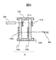
- the light guide plate is composed of a plurality of uneven diffraction gratings formed on a glass substrate.
- the light beam emitted from the projector is coupled to the light guide plate by an incident diffraction grating and propagates inside the light guide plate while being totally reflected.
- the light beam is totally reflected and propagated in the light guide plate while being converted into a plurality of light rays duplicated by yet another diffraction grating, and finally emitted from the light guide plate.
- a part of the emitted light rays is imaged on the retina through the user's pupil and recognized as an augmented reality image superimposed on the image in the real world.
- the function of the light guide plate is to guide the light rays emitted from the projector while replicating them in multiple ways so that the user can recognize the multiple light rays emitted as image information equivalent to the original image.
- the duplicated ray group has a wave number vector equivalent to the ray having the image information emitted from the projector, and has a spatial spread.
- a part of the duplicated ray group enters the pupil and is visually recognized by being imaged on the retina together with the information of the outside world, and can provide the user with information of augmented reality in addition to the information of the outside world.
- the light rays are duplicated and spatially spread and emitted. Therefore, the larger the spatial spread, the smaller the visible light rays and the smaller the visible brightness.
- the emission position visually recognized by the user changes depending on the pixel position of the original video information, it is inevitable that the brightness changes depending on the pixel position in the image display device using the light guide plate.
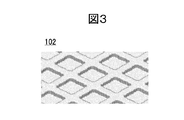
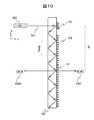
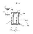
- FIG. 7 is a schematic plan view of one light guide plate 100, and shows an example of the relationship between the wave number vectors of the formed incident diffraction grating 101 and the emission diffraction grating 102.
- 100 light guide plate
- 101 incident diffraction grating
- 102 exit diffraction grating
- 300 projector
- 400 user's pupil
Landscapes
- Physics & Mathematics (AREA)
- General Physics & Mathematics (AREA)
- Optics & Photonics (AREA)
- Engineering & Computer Science (AREA)
- Computer Graphics (AREA)
- Computer Hardware Design (AREA)
- General Engineering & Computer Science (AREA)
- Software Systems (AREA)
- Theoretical Computer Science (AREA)
- Multimedia (AREA)
- Signal Processing (AREA)
- Diffracting Gratings Or Hologram Optical Elements (AREA)
Priority Applications (2)
| Application Number | Priority Date | Filing Date | Title |
|---|---|---|---|
| US17/785,102 US20230028757A1 (en) | 2020-01-10 | 2020-10-08 | Image display element, image display device, and image display method |
| CN202080089130.0A CN114846387B (zh) | 2020-01-10 | 2020-10-08 | 图像显示元件、图像显示装置以及图像显示方法 |
Applications Claiming Priority (2)
| Application Number | Priority Date | Filing Date | Title |
|---|---|---|---|
| JP2020-002824 | 2020-01-10 | ||
| JP2020002824A JP7341906B2 (ja) | 2020-01-10 | 2020-01-10 | 画像表示素子、画像表示装置および画像表示方法 |
Publications (1)
| Publication Number | Publication Date |
|---|---|
| WO2021140716A1 true WO2021140716A1 (ja) | 2021-07-15 |
Family
ID=76788156
Family Applications (1)
| Application Number | Title | Priority Date | Filing Date |
|---|---|---|---|
| PCT/JP2020/038160 Ceased WO2021140716A1 (ja) | 2020-01-10 | 2020-10-08 | 画像表示素子、画像表示装置および画像表示方法 |
Country Status (5)
| Country | Link |
|---|---|
| US (1) | US20230028757A1 (https=) |
| JP (1) | JP7341906B2 (https=) |
| CN (1) | CN114846387B (https=) |
| TW (1) | TW202127107A (https=) |
| WO (1) | WO2021140716A1 (https=) |
Cited By (1)
| Publication number | Priority date | Publication date | Assignee | Title |
|---|---|---|---|---|
| CN114089476A (zh) * | 2021-11-25 | 2022-02-25 | Oppo广东移动通信有限公司 | 光波导镜片、制备光波导镜片的方法、增强现实设备 |
Families Citing this family (6)
| Publication number | Priority date | Publication date | Assignee | Title |
|---|---|---|---|---|
| JP7465826B2 (ja) * | 2021-02-02 | 2024-04-11 | 株式会社日立エルジーデータストレージ | 導光板、導光板モジュールおよび画像表示装置 |
| CN115685573B (zh) * | 2022-11-07 | 2026-02-06 | 湖北长江新型显示产业创新中心有限公司 | 一种场镜、显示装置及电子设备 |
| CN115951438B (zh) * | 2022-12-30 | 2026-03-31 | 上海天马微电子有限公司 | 场镜和显示装置 |
| CN119224912A (zh) * | 2023-06-29 | 2024-12-31 | 歌尔光学科技(上海)有限公司 | 导光器件、光学模组以及头戴显示设备 |
| TWI880517B (zh) * | 2023-12-12 | 2025-04-11 | 國立中央大學 | 混合實境顯示裝置 |
| CN120871331B (zh) * | 2025-09-26 | 2026-03-27 | 歌尔股份有限公司 | 光波导结构、光学模组及智能眼镜 |
Citations (4)
| Publication number | Priority date | Publication date | Assignee | Title |
|---|---|---|---|---|
| JP2006065312A (ja) * | 2004-07-26 | 2006-03-09 | Nippon Sheet Glass Co Ltd | 透過型回折光学素子 |
| US20100277803A1 (en) * | 2006-12-14 | 2010-11-04 | Nokia Corporation | Display Device Having Two Operating Modes |
| US20150293357A1 (en) * | 2012-10-18 | 2015-10-15 | Lg Electronics Inc. | Optical device |
| JP2017156388A (ja) * | 2016-02-29 | 2017-09-07 | セイコーエプソン株式会社 | 光束径拡大素子及び画像表示装置 |
Family Cites Families (8)
| Publication number | Priority date | Publication date | Assignee | Title |
|---|---|---|---|---|
| JP3623250B2 (ja) * | 1993-06-23 | 2005-02-23 | オリンパス株式会社 | 映像表示装置 |
| EP1622137A1 (en) * | 2003-04-25 | 2006-02-01 | Matsushita Electric Industrial Co., Ltd. | Optical diffraction device and optical information processing device |
| JP2005135899A (ja) * | 2003-10-06 | 2005-05-26 | Omron Corp | 面光源装置及び表示装置 |
| JP4163729B2 (ja) | 2006-10-03 | 2008-10-08 | 株式会社東芝 | 磁気記録媒体、その製造方法、および磁気記録装置 |
| WO2011007878A1 (ja) * | 2009-07-16 | 2011-01-20 | Jx日鉱日石エネルギー株式会社 | 回折格子及びそれを用いた有機el素子、並びにそれらの製造方法 |
| KR101552172B1 (ko) * | 2011-03-28 | 2015-09-10 | 제이엑스 닛코닛세키 에네루기 가부시키가이샤 | 요철 구조를 가지는 기판 제조 방법 및 이것을 사용한 유기 el 소자의 제조 방법 |
| RU2695941C2 (ru) | 2014-12-24 | 2019-07-29 | Конинклейке Филипс Н.В. | Автостереоскопическое дисплейное устройство и способ возбуждения |
| EP3642652B1 (en) * | 2017-06-19 | 2026-01-21 | Magic Leap, Inc. | Eyepiece comprising a dynamically actuable diffractive optical element |
-
2020
- 2020-01-10 JP JP2020002824A patent/JP7341906B2/ja active Active
- 2020-10-08 WO PCT/JP2020/038160 patent/WO2021140716A1/ja not_active Ceased
- 2020-10-08 CN CN202080089130.0A patent/CN114846387B/zh not_active Expired - Fee Related
- 2020-10-08 US US17/785,102 patent/US20230028757A1/en not_active Abandoned
- 2020-10-20 TW TW109136215A patent/TW202127107A/zh unknown
Patent Citations (4)
| Publication number | Priority date | Publication date | Assignee | Title |
|---|---|---|---|---|
| JP2006065312A (ja) * | 2004-07-26 | 2006-03-09 | Nippon Sheet Glass Co Ltd | 透過型回折光学素子 |
| US20100277803A1 (en) * | 2006-12-14 | 2010-11-04 | Nokia Corporation | Display Device Having Two Operating Modes |
| US20150293357A1 (en) * | 2012-10-18 | 2015-10-15 | Lg Electronics Inc. | Optical device |
| JP2017156388A (ja) * | 2016-02-29 | 2017-09-07 | セイコーエプソン株式会社 | 光束径拡大素子及び画像表示装置 |
Cited By (1)
| Publication number | Priority date | Publication date | Assignee | Title |
|---|---|---|---|---|
| CN114089476A (zh) * | 2021-11-25 | 2022-02-25 | Oppo广东移动通信有限公司 | 光波导镜片、制备光波导镜片的方法、增强现实设备 |
Also Published As
| Publication number | Publication date |
|---|---|
| TW202127107A (zh) | 2021-07-16 |
| CN114846387A (zh) | 2022-08-02 |
| US20230028757A1 (en) | 2023-01-26 |
| CN114846387B (zh) | 2023-11-14 |
| JP2021110837A (ja) | 2021-08-02 |
| JP7341906B2 (ja) | 2023-09-11 |
Similar Documents
| Publication | Publication Date | Title |
|---|---|---|
| JP7297548B2 (ja) | 導光板の製造方法、導光板モジュールの製造方法、および画像表示装置の製造方法 | |
| CN111190288B (zh) | 导光板及图像显示装置 | |
| JP7341906B2 (ja) | 画像表示素子、画像表示装置および画像表示方法 | |
| US20200012031A1 (en) | Image display device | |
| JP7341907B2 (ja) | 画像表示素子および装置 | |
| EP4310576B1 (en) | Diffractive optical waveguide and display device | |
| JP7096084B2 (ja) | 導光板、導光板モジュール、画像表示装置および導光板の製造方法 | |
| US12306410B2 (en) | Display apparatus including volume grating based combiner | |
| CN113759550B (zh) | 用于提供扩展观看窗的显示装置 | |
| JP7465826B2 (ja) | 導光板、導光板モジュールおよび画像表示装置 |
Legal Events
| Date | Code | Title | Description |
|---|---|---|---|
| 121 | Ep: the epo has been informed by wipo that ep was designated in this application |
Ref document number: 20912025 Country of ref document: EP Kind code of ref document: A1 |
|
| NENP | Non-entry into the national phase |
Ref country code: DE |
|
| 122 | Ep: pct application non-entry in european phase |
Ref document number: 20912025 Country of ref document: EP Kind code of ref document: A1 |