WO2021132257A1 - Film capacitor and film for film capacitors - Google Patents
Film capacitor and film for film capacitors Download PDFInfo
- Publication number
- WO2021132257A1 WO2021132257A1 PCT/JP2020/047994 JP2020047994W WO2021132257A1 WO 2021132257 A1 WO2021132257 A1 WO 2021132257A1 JP 2020047994 W JP2020047994 W JP 2020047994W WO 2021132257 A1 WO2021132257 A1 WO 2021132257A1
- Authority
- WO
- WIPO (PCT)
- Prior art keywords
- film
- organic material
- linear expansion
- metal layer
- dielectric resin
- Prior art date
Links
- 239000003990 capacitor Substances 0.000 title claims abstract description 70
- 229920005989 resin Polymers 0.000 claims abstract description 64
- 239000011347 resin Substances 0.000 claims abstract description 64
- 239000011368 organic material Substances 0.000 claims abstract description 51
- 239000002184 metal Substances 0.000 claims abstract description 47
- 229910052751 metal Inorganic materials 0.000 claims abstract description 47
- UPMLOUAZCHDJJD-UHFFFAOYSA-N 4,4'-Diphenylmethane Diisocyanate Chemical compound C1=CC(N=C=O)=CC=C1CC1=CC=C(N=C=O)C=C1 UPMLOUAZCHDJJD-UHFFFAOYSA-N 0.000 claims abstract description 13
- 125000002887 hydroxy group Chemical group [H]O* 0.000 claims abstract description 13
- 239000000203 mixture Substances 0.000 claims abstract description 8
- 229920000620 organic polymer Polymers 0.000 claims abstract description 6
- 125000001997 phenyl group Chemical group [H]C1=C([H])C([H])=C(*)C([H])=C1[H] 0.000 claims abstract description 6
- HIFVAOIJYDXIJG-UHFFFAOYSA-N benzylbenzene;isocyanic acid Chemical class N=C=O.N=C=O.C=1C=CC=CC=1CC1=CC=CC=C1 HIFVAOIJYDXIJG-UHFFFAOYSA-N 0.000 claims abstract 3
- 229920006287 phenoxy resin Polymers 0.000 claims description 4
- 239000013034 phenoxy resin Substances 0.000 claims description 4
- 239000010408 film Substances 0.000 description 171
- ZWEHNKRNPOVVGH-UHFFFAOYSA-N 2-Butanone Chemical compound CCC(C)=O ZWEHNKRNPOVVGH-UHFFFAOYSA-N 0.000 description 21
- 239000011104 metalized film Substances 0.000 description 17
- WYURNTSHIVDZCO-UHFFFAOYSA-N Tetrahydrofuran Chemical compound C1CCOC1 WYURNTSHIVDZCO-UHFFFAOYSA-N 0.000 description 14
- 230000015556 catabolic process Effects 0.000 description 12
- 238000004804 winding Methods 0.000 description 10
- 239000002904 solvent Substances 0.000 description 7
- YLQBMQCUIZJEEH-UHFFFAOYSA-N tetrahydrofuran Natural products C=1C=COC=1 YLQBMQCUIZJEEH-UHFFFAOYSA-N 0.000 description 7
- IQPQWNKOIGAROB-UHFFFAOYSA-N isocyanate group Chemical group [N-]=C=O IQPQWNKOIGAROB-UHFFFAOYSA-N 0.000 description 6
- 238000000034 method Methods 0.000 description 5
- 230000000052 comparative effect Effects 0.000 description 4
- 238000005259 measurement Methods 0.000 description 4
- PXHVJJICTQNCMI-UHFFFAOYSA-N Nickel Chemical compound [Ni] PXHVJJICTQNCMI-UHFFFAOYSA-N 0.000 description 3
- 239000000654 additive Substances 0.000 description 3
- 239000008199 coating composition Substances 0.000 description 3
- 238000001035 drying Methods 0.000 description 3
- 125000000524 functional group Chemical group 0.000 description 3
- 238000004519 manufacturing process Methods 0.000 description 3
- 238000005507 spraying Methods 0.000 description 3
- 229920001187 thermosetting polymer Polymers 0.000 description 3
- 238000005033 Fourier transform infrared spectroscopy Methods 0.000 description 2
- 230000000996 additive effect Effects 0.000 description 2
- 229910052782 aluminium Inorganic materials 0.000 description 2
- XAGFODPZIPBFFR-UHFFFAOYSA-N aluminium Chemical compound [Al] XAGFODPZIPBFFR-UHFFFAOYSA-N 0.000 description 2
- 230000007423 decrease Effects 0.000 description 2
- -1 isocyanate compound Chemical class 0.000 description 2
- 238000010030 laminating Methods 0.000 description 2
- 239000011777 magnesium Substances 0.000 description 2
- 239000000463 material Substances 0.000 description 2
- 239000012046 mixed solvent Substances 0.000 description 2
- 229920000139 polyethylene terephthalate Polymers 0.000 description 2
- 239000005020 polyethylene terephthalate Substances 0.000 description 2
- 230000000930 thermomechanical effect Effects 0.000 description 2
- 239000010936 titanium Substances 0.000 description 2
- 229920002799 BoPET Polymers 0.000 description 1
- FYYHWMGAXLPEAU-UHFFFAOYSA-N Magnesium Chemical compound [Mg] FYYHWMGAXLPEAU-UHFFFAOYSA-N 0.000 description 1
- 239000004640 Melamine resin Substances 0.000 description 1
- 229920000877 Melamine resin Polymers 0.000 description 1
- ATJFFYVFTNAWJD-UHFFFAOYSA-N Tin Chemical compound [Sn] ATJFFYVFTNAWJD-UHFFFAOYSA-N 0.000 description 1
- RTAQQCXQSZGOHL-UHFFFAOYSA-N Titanium Chemical compound [Ti] RTAQQCXQSZGOHL-UHFFFAOYSA-N 0.000 description 1
- HCHKCACWOHOZIP-UHFFFAOYSA-N Zinc Chemical compound [Zn] HCHKCACWOHOZIP-UHFFFAOYSA-N 0.000 description 1
- 238000004458 analytical method Methods 0.000 description 1
- 230000015572 biosynthetic process Effects 0.000 description 1
- IISBACLAFKSPIT-UHFFFAOYSA-N bisphenol A Chemical group C=1C=C(O)C=CC=1C(C)(C)C1=CC=C(O)C=C1 IISBACLAFKSPIT-UHFFFAOYSA-N 0.000 description 1
- 125000003178 carboxy group Chemical group [H]OC(*)=O 0.000 description 1
- 239000003795 chemical substances by application Substances 0.000 description 1
- 239000011248 coating agent Substances 0.000 description 1
- 238000000576 coating method Methods 0.000 description 1
- 230000007547 defect Effects 0.000 description 1
- 230000005684 electric field Effects 0.000 description 1
- 125000003700 epoxy group Chemical group 0.000 description 1
- 239000003822 epoxy resin Substances 0.000 description 1
- 239000012948 isocyanate Substances 0.000 description 1
- 229910052749 magnesium Inorganic materials 0.000 description 1
- 238000002156 mixing Methods 0.000 description 1
- 238000000465 moulding Methods 0.000 description 1
- 229910052759 nickel Inorganic materials 0.000 description 1
- 239000012788 optical film Substances 0.000 description 1
- 229920000647 polyepoxide Polymers 0.000 description 1
- 229920005862 polyol Polymers 0.000 description 1
- 150000003077 polyols Chemical class 0.000 description 1
- 229920001296 polysiloxane Polymers 0.000 description 1
- 238000002360 preparation method Methods 0.000 description 1
- 239000011342 resin composition Substances 0.000 description 1
- 125000005372 silanol group Chemical group 0.000 description 1
- 239000007858 starting material Substances 0.000 description 1
- JBQYATWDVHIOAR-UHFFFAOYSA-N tellanylidenegermanium Chemical compound [Te]=[Ge] JBQYATWDVHIOAR-UHFFFAOYSA-N 0.000 description 1
- 238000007751 thermal spraying Methods 0.000 description 1
- 229920005992 thermoplastic resin Polymers 0.000 description 1
- 238000000427 thin-film deposition Methods 0.000 description 1
- 229910052719 titanium Inorganic materials 0.000 description 1
- 239000011701 zinc Substances 0.000 description 1
- 229910052725 zinc Inorganic materials 0.000 description 1
Images


Classifications
-
- H—ELECTRICITY
- H01—ELECTRIC ELEMENTS
- H01G—CAPACITORS; CAPACITORS, RECTIFIERS, DETECTORS, SWITCHING DEVICES OR LIGHT-SENSITIVE DEVICES, OF THE ELECTROLYTIC TYPE
- H01G4/00—Fixed capacitors; Processes of their manufacture
- H01G4/33—Thin- or thick-film capacitors
-
- H—ELECTRICITY
- H01—ELECTRIC ELEMENTS
- H01G—CAPACITORS; CAPACITORS, RECTIFIERS, DETECTORS, SWITCHING DEVICES OR LIGHT-SENSITIVE DEVICES, OF THE ELECTROLYTIC TYPE
- H01G4/00—Fixed capacitors; Processes of their manufacture
- H01G4/002—Details
- H01G4/018—Dielectrics
- H01G4/06—Solid dielectrics
- H01G4/14—Organic dielectrics
- H01G4/18—Organic dielectrics of synthetic material, e.g. derivatives of cellulose
-
- H—ELECTRICITY
- H01—ELECTRIC ELEMENTS
- H01G—CAPACITORS; CAPACITORS, RECTIFIERS, DETECTORS, SWITCHING DEVICES OR LIGHT-SENSITIVE DEVICES, OF THE ELECTROLYTIC TYPE
- H01G4/00—Fixed capacitors; Processes of their manufacture
- H01G4/32—Wound capacitors
Definitions
- the present invention relates to a film capacitor and a film for a film capacitor.
- a film capacitor having a structure in which a first counter electrode and a second counter electrode are arranged so as to face each other with the resin film sandwiched between them while using a flexible resin film as a dielectric.
- Such a film capacitor is produced, for example, by winding or laminating a resin film on which a first counter electrode is formed and a resin film on which a second counter electrode is formed.
- Patent Documents 1 to 3 describe that a dielectric resin film made of a curable resin such as a thermosetting resin is used.
- Patent Document 1 describes a cured product obtained by reacting at least two kinds of organic materials including the first and second organic materials, the first organic material being a polyol, and the second organic material.
- the organic material of the above is an isocyanate compound, an epoxy resin or a melamine resin having a plurality of functional groups in the molecule.
- a dielectric resin film using a curable resin such as a thermosetting resin has a feature of having higher heat resistance and withstand voltage than a dielectric resin film using a thermoplastic resin.
- Patent Document 3 describes that the dielectric breakdown strength of a film at 125 ° C. is 300 V / ⁇ m or more as the withstand voltage strength of the film.
- the withstand voltage strength in a higher temperature region has not been examined.
- the present invention has been made to solve the above problems, and an object of the present invention is to provide a film capacitor including a dielectric resin film having a high dielectric breakdown strength at 145 ° C. It is also an object of the present invention to provide a film for the film capacitor.
- the film capacitor of the present invention includes a dielectric resin film made of a cured product of a first organic material and a second organic material, and a metal layer provided on at least one surface of the dielectric resin film.
- the first organic material is composed of an organic polymer having a hydroxyl group and a benzene ring in a repeating unit.
- the second organic material comprises diphenylmethane diisocyanate, a modified diphenylmethane diisocyanate, or a mixture thereof.
- the linear expansion coefficient at 40 ° C is ⁇ 40 ° C
- the linear expansion coefficient at 80 ° C is ⁇ 80 ° C
- the linear expansion coefficient at 120 ° C is ⁇ .
- ⁇ is 120 ° C.
- the value of ⁇ 40 ° C./ ⁇ 80 ° C. is 1.05 or more
- the value of ⁇ 80 ° C./ ⁇ 120 ° C. is 1.1 or more.
- the film for a film capacitor of the present invention comprises a cured product of a first organic material and a second organic material.
- the first organic material is composed of an organic polymer having a hydroxyl group and a benzene ring in a repeating unit.
- the second organic material comprises diphenylmethane diisocyanate, a modified diphenylmethane diisocyanate, or a mixture thereof.
- the linear expansion coefficient at 40 ° C is ⁇ 40 ° C
- the linear expansion coefficient at 80 ° C is ⁇ 80 ° C
- the linear expansion coefficient at 120 ° C is ⁇ .
- the value of ⁇ 40 ° C./ ⁇ 80 ° C. is 1.05 or more
- the value of ⁇ 80 ° C./ ⁇ 120 ° C. is 1.1 or more.
- a film capacitor including a dielectric resin film having a high dielectric breakdown strength at 145 ° C.
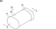
- FIG. 1 is a perspective view schematically showing an example of the film capacitor of the present invention.
- FIG. 2 is a sectional view taken along line II-II of the film capacitor shown in FIG.
- FIG. 3 is a perspective view schematically showing an example of a wound body of a metallized film constituting the film capacitors shown in FIGS. 1 and 2.
- the film capacitor of the present invention and the film for a film capacitor will be described.
- the present invention is not limited to the following configurations, and can be appropriately modified and applied without changing the gist of the present invention.
- a combination of two or more of the individual desirable configurations of the invention described below is also the invention.
- the film capacitor of the present invention includes a dielectric resin film and a metal layer provided on at least one surface of the dielectric resin film.
- the film capacitor of the present invention has, for example, a columnar column having an elongated cross section, and external terminal electrodes formed by, for example, metal spraying (metallic spraying) are provided at both ends in the direction of the central axis.
- a first dielectric resin film provided with a first metal layer and a second dielectric resin film provided with a second metal layer are laminated.
- a winding type film capacitor, which is wound in a wound state will be described as an example.
- the film capacitor of the present invention is a laminated type in which a first dielectric resin film provided with a first metal layer and a second dielectric resin film provided with a second metal layer are laminated. It may be a film capacitor or the like. Further, in the film capacitor of the present invention, a first dielectric resin film provided with a first metal layer and a second metal layer and a second dielectric resin film not provided with a metal layer are wound. It may be a film capacitor that has been rotated or laminated.
- FIG. 1 is a perspective view schematically showing an example of the film capacitor of the present invention.
- FIG. 2 is a sectional view taken along line II-II of the film capacitor shown in FIG.
- the film capacitor 10 shown in FIGS. 1 and 2 is a winding type film capacitor, and is a metallized film wound in a state in which a first metallized film 11 and a second metallized film 12 are laminated. 40, and a first external terminal electrode 41 and a second external terminal electrode 42 connected to both ends of the metallized film winding body 40 are provided.
- the first metallized film 11 is a first metal layer (counter electrode) provided on one surface of a first dielectric resin film 13 and a first dielectric resin film 13.
- the second metallized film 12 is a second metal layer (counter electrode) provided on one surface of the second dielectric resin film 14 and the second dielectric resin film 14. It has 16.
- the first metal layer 15 and the second metal layer 16 face each other with the first dielectric resin film 13 or the second dielectric resin film 14 interposed therebetween. Further, the first metal layer 15 is electrically connected to the first external terminal electrode 41, and the second metal layer 16 is electrically connected to the second external terminal electrode 42.
- the first dielectric resin film 13 and the second dielectric resin film 14 may have different configurations, but it is desirable that they have the same configuration.
- the first metal layer 15 is formed so as to reach one side edge on one surface of the first dielectric resin film 13 but not to the other side edge.
- the second metal layer 16 is formed so as not to reach one side edge on one surface of the second dielectric resin film 14, but to reach the other side edge.
- the first metal layer 15 and the second metal layer 16 are composed of, for example, an aluminum layer.
- FIG. 3 is a perspective view schematically showing an example of a wound body of a metallized film constituting the film capacitors shown in FIGS. 1 and 2.
- the end of the first metal layer 15 on the side reaching the side edge of the first dielectric resin film 13 and the second end of the second metal layer 16 The width of the first dielectric resin film 13 and the width of the second dielectric resin film 14 are such that the end portions on the side reaching the side edge of the dielectric resin film 14 are exposed from the laminated film.
- the layers are stacked so as to be shifted in the direction (left-right direction in FIG. 2).
- the wound body 40 of the metallized film is formed, and the first metal layer 15 and the second metal are formed.
- the layers 16 are held in a state of being exposed at the ends and are in a stacked state.
- the second dielectric resin film 14 is located outside the first dielectric resin film 13, and the first dielectric resin film 13 and the second dielectric resin film 14 are formed.
- Each of the first metal layer 15 and the second metal layer 16 is wound so as to face inward.
- the first external terminal electrode 41 and the second external terminal electrode 42 are formed by spraying, for example, zinc or the like onto each end surface of the wound body 40 of the metallized film obtained as described above. ..
- the first external terminal electrode 41 comes into contact with the exposed end of the first metal layer 15 and is thereby electrically connected to the first metal layer 15.
- the second external terminal electrode 42 comes into contact with the exposed end of the second metal layer 16 and is thereby electrically connected to the second metal layer 16.
- the wound body of the metallized film is pressed into a flat shape such as an ellipse or an oval, and has a more compact shape than when the cross-sectional shape is a perfect circle. ..
- the film capacitor of the present invention may include a cylindrical winding shaft.
- the winding shaft is arranged on the central axis of the metallized film in the wound state, and serves as a winding shaft when the metallized film is wound.
- examples of the metal contained in the metal layer include aluminum (Al), titanium (Ti), zinc (Zn), magnesium (Mg), tin (Sn), nickel (Ni) and the like. Be done.
- the thickness of the metal layer is not particularly limited, but is, for example, 5 nm or more and 40 nm or less.
- the thickness of the metal layer is specified by observing a cross section of a dielectric resin film provided with the metal layer cut in the thickness direction using an electron microscope such as a field emission scanning electron microscope (FE-SEM). can do.
- FE-SEM field emission scanning electron microscope
- the metal layer is provided with a fuse portion.
- the fuse portion means a portion where the metal layer serving as the counter electrode is divided into a plurality of electrodes and the electrode portion is connected to the electrode portion.
- the pattern of the metal layer having the fuse portion is not particularly limited, and for example, the electrode patterns disclosed in JP-A-2004-363431, JP-A-5-251266 and the like can be used.
- the film for the film capacitor of the present invention is used as the dielectric resin film.
- the film for a film capacitor of the present invention may be used for both the first dielectric resin film 13 and the second dielectric resin film 14.
- the film for a film capacitor of the present invention may be used for only one of them.
- the film for a film capacitor of the present invention comprises a cured product of a first organic material and a second organic material.
- the film for a film capacitor of the present invention is made of a cured product obtained by reacting a hydroxyl group (OH group) of a first organic material with an isocyanate group (NCO group) of a second organic material.
- the first organic material is composed of an organic polymer having a hydroxyl group and a benzene ring in a repeating unit.
- the first organic material is preferably made of a phenoxy resin.
- the second organic material consists of diphenylmethane diisocyanate, a modified diphenylmethane diisocyanate, or a mixture thereof.
- the second organic material is preferably composed of 4,4'-diphenylmethane diisocyanate, a modified 4,4'-diphenylmethane diisocyanate, or a mixture thereof.
- the film for a film capacitor of the present invention may contain at least one of a hydroxyl group and an isocyanate group.
- the film for a film capacitor of the present invention may contain either a hydroxyl group or an isocyanate group, or may contain both a hydroxyl group and an isocyanate group.
- FT-IR Fourier transform infrared spectrophotometer
- the coefficient of linear expansion at 40 ° C is ⁇ 40 ° C
- the coefficient of linear expansion at 80 ° C is ⁇ 80 ° C, 120 ° C.
- the coefficient of linear expansion is ⁇ 120 ° C.
- the value of ⁇ 40 ° C./ ⁇ 80 ° C. is 1.05 or more
- the value of ⁇ 80 ° C./ ⁇ 120 ° C. is 1.1 or more.
- the dielectric breakdown strength at 145 ° C. is 300 V / ⁇ m or more.
- the coefficient of linear expansion of the film is a value calculated from the rate of change in length from 0 ° C to each temperature of the film by the thermomechanical analysis (TMA) method.
- ⁇ 40 ° C./ ⁇ 80 ° C. is 1.05 or more.
- the value of ⁇ 40 ° C./ ⁇ 80 ° C. is, for example, 1.35 or less.
- ⁇ 80 ° C./ ⁇ 120 ° C. is 1.1 or more, preferably 1.15 or more.
- the value of ⁇ 80 ° C./ ⁇ 120 ° C. is, for example, 1.40 or less.
- ⁇ 40 ° C./ ⁇ 120 ° C. is not particularly limited, but is preferably 1.2 or more, and more preferably 1.25 or more. On the other hand, the value of ⁇ 40 ° C./ ⁇ 120 ° C. is, for example, 1.50 or less.
- the film for a film capacitor of the present invention may also contain an additive for adding other functions.
- smoothness can be imparted by adding a leveling agent.
- the additive is a material that has a functional group that reacts with a hydroxyl group and / or an isocyanate group and forms a part of the crosslinked structure of the cured product. Examples of such a material include a resin having at least one functional group selected from the group consisting of an epoxy group, a silanol group and a carboxyl group.
- the thickness of the film for a film capacitor of the present invention is not particularly limited, but if the film is too thin, it tends to become brittle. Therefore, the thickness of the film for a film capacitor of the present invention is preferably 1 ⁇ m or more, and more preferably 3 ⁇ m or more. On the other hand, if the film is too thick, defects such as cracks are likely to occur during film formation. Therefore, the thickness of the film for a film capacitor of the present invention is preferably 10 ⁇ m or less, and more preferably 5 ⁇ m or less.
- the thickness of the film means the thickness of the film alone, not including the thickness of the metal layer. The thickness of the film can be measured using an optical film thickness meter.
- the film for a film capacitor of the present invention is obtained by molding a resin solution containing a first organic material and a second organic material into a film, and then heat-treating and curing the resin solution.
- the resin solution is prepared, for example, by dissolving the above-mentioned first organic material and second organic material in a solvent, mixing them, and adding additives as necessary.
- the solvent contained in the resin solution may be present as a residue in the cured film.
- the weight ratio of the first organic material to the second organic material is preferably 50/50 or more and 75/25 or less.
- the solvent it is preferable to use a mixed solvent containing methyl ethyl ketone (MEK) and tetrahydrofuran (THF).
- MEK methyl ethyl ketone
- THF tetrahydrofuran
- the weight ratio of MEK to THF (MEK / THF) is preferably 15/85 or more and 85/15 or less.
- a metallized film is obtained by using the film for a film capacitor of the present invention as a dielectric resin film and forming a metal layer on one surface of the dielectric resin film.
- the method for forming the metal layer include a method such as thin film deposition.
- a laminated body is obtained by laminating two metallized films having a metal layer formed on one surface of a dielectric resin film in a state of being shifted by a predetermined distance in the width direction and then winding the film. If necessary, the laminate may be sandwiched from a direction perpendicular to the width direction and pressed into an elliptical cylinder shape.
- a film capacitor as shown in FIG. 1 can be obtained.
- thermal spraying can be mentioned.
- Example 1 As the first organic material, a phenoxy resin having a bisphenol A skeleton was prepared, and as the second organic material, a mixture of 4,4'-diphenylmethane diisocyanate (MDI) and a modified product thereof was prepared.
- MDI 4,4'-diphenylmethane diisocyanate
- the first organic material and the second organic material are dissolved in a mixed solvent of MEK and THF and mixed, and a silicone-based surface conditioner BYK370 (manufactured by Big Chemie Japan Co., Ltd.) is further added to the coating composition ( Resin solution) was prepared.
- the coating composition is coated on a polyethylene terephthalate (PET) film which is a base film, and after coating, a hot air of 70 ° C. is applied to dry the solvent, and then the coating composition is peeled off from the PET film to make the thickness. A 3 ⁇ m film was formed. The obtained film was heat-treated at 150 ° C. for 4 hours to cure.
- PET polyethylene terephthalate
- Example 1 As described above, the sample of Example 1 was prepared.
- Example 2 A sample was prepared in the same manner as in Example 1 except that the drying temperature of the solvent was changed from 70 ° C. to 100 ° C.
- Example 1 A sample was prepared in the same manner as in Example 1 except that the drying temperature of the solvent was changed from 70 ° C. to 140 ° C.
- Example 2 A sample was prepared in the same manner as in Example 1 except that the drying temperature of the solvent was changed from 70 ° C. to 180 ° C.
- the dielectric breakdown strength at 145 ° C. is 300 V. It was less than / ⁇ m.
- Film capacitor 11 First metallized film 12 Second metallized film 13 First dielectric resin film 14 Second dielectric resin film 15 First metal layer 16 Second metal layer 40 Metallic film Winding body 41 First external terminal electrode 42 Second external terminal electrode
Abstract
This film capacitor 10 is provided with: a dielectric resin film (for example, a first dielectric resin film 13) which is formed of a cured product of a first organic material and a second organic material; and a metal layer (for example, a first metal layer 15) which is arranged on at least one surface of the dielectric resin film. The first organic material is composed of an organic polymer that has a hydroxyl group and a benzene ring in a repeating unit. The second organic material is composed of diphenylmethane diisocyanate, a modified diphenylmethane diisocyanate or a mixture thereof. Among the linear expansion coefficients of the above-described film based on that at 0°C, if α40°C is the linear expansion coefficient at 40°C, α80°C is the linear expansion coefficient at 80°C and α120°C is the linear expansion coefficient at 120°C, the value of α40°C/α80°C is 1.05 or more, and the value of α80°C/α120°C is 1.1 or more.
Description
本発明は、フィルムコンデンサ、及び、フィルムコンデンサ用フィルムに関する。
The present invention relates to a film capacitor and a film for a film capacitor.
コンデンサの一種として、可撓性のある樹脂フィルムを誘電体として用いながら、樹脂フィルムを挟んで互いに対向する第1の対向電極及び第2の対向電極を配置した構造のフィルムコンデンサがある。このようなフィルムコンデンサは、例えば、第1の対向電極が形成された樹脂フィルムと第2の対向電極が形成された樹脂フィルムとを巻回又は積層することによって作製される。
As a kind of capacitor, there is a film capacitor having a structure in which a first counter electrode and a second counter electrode are arranged so as to face each other with the resin film sandwiched between them while using a flexible resin film as a dielectric. Such a film capacitor is produced, for example, by winding or laminating a resin film on which a first counter electrode is formed and a resin film on which a second counter electrode is formed.
フィルムコンデンサ用の誘電体樹脂フィルムとして、特許文献1~3には、熱硬化性樹脂などの硬化性樹脂からなる誘電体樹脂フィルムを用いることが記載されている。例えば、特許文献1には、第1および第2の有機材料を含む少なくとも2種類の有機材料が反応して得られた硬化物であり、上記第1の有機材料がポリオールであり、上記第2の有機材料が、分子内に複数の官能基を持つ、イソシアネート化合物、またはエポキシ樹脂もしくはメラミン樹脂である、フィルムコンデンサ用誘電体樹脂組成物が開示されている。
As a dielectric resin film for a film capacitor, Patent Documents 1 to 3 describe that a dielectric resin film made of a curable resin such as a thermosetting resin is used. For example, Patent Document 1 describes a cured product obtained by reacting at least two kinds of organic materials including the first and second organic materials, the first organic material being a polyol, and the second organic material. Disclosed is a dielectric resin composition for a film capacitor, wherein the organic material of the above is an isocyanate compound, an epoxy resin or a melamine resin having a plurality of functional groups in the molecule.
熱硬化性樹脂などの硬化性樹脂を用いた誘電体樹脂フィルムは、熱可塑性樹脂を用いた誘電体樹脂フィルムに比べて耐熱性及び耐電圧性が高いという特徴を有している。例えば、特許文献3には、フィルムの耐電圧強度として、125℃における絶縁破壊強度が300V/μm以上であることが記載されている。しかしながら、特許文献1~3においては、より高い温度領域における耐電圧強度については検討されていなかった。
A dielectric resin film using a curable resin such as a thermosetting resin has a feature of having higher heat resistance and withstand voltage than a dielectric resin film using a thermoplastic resin. For example, Patent Document 3 describes that the dielectric breakdown strength of a film at 125 ° C. is 300 V / μm or more as the withstand voltage strength of the film. However, in Patent Documents 1 to 3, the withstand voltage strength in a higher temperature region has not been examined.
本発明は、上記の問題を解決するためになされたものであり、145℃における絶縁破壊強度が高い誘電体樹脂フィルムを備えるフィルムコンデンサを提供することを目的とする。本発明はまた、上記フィルムコンデンサ用フィルムを提供することを目的とする。
The present invention has been made to solve the above problems, and an object of the present invention is to provide a film capacitor including a dielectric resin film having a high dielectric breakdown strength at 145 ° C. It is also an object of the present invention to provide a film for the film capacitor.
本発明のフィルムコンデンサは、第1有機材料と第2有機材料との硬化物からなる誘電体樹脂フィルムと、上記誘電体樹脂フィルムの少なくとも一方の面に設けられた金属層と、を備える。上記第1有機材料は、繰り返し単位の中に水酸基とベンゼン環とを有する有機高分子からなる。上記第2有機材料は、ジフェニルメタンジイソシアネート、ジフェニルメタンジイソシアネート変性体、又は、これらの混合物からなる。上記フィルムの0℃を基準とした線膨張係数のうち、40℃のときの線膨張係数をα40℃、80℃のときの線膨張係数をα80℃、120℃のときの線膨張係数をα120℃としたとき、α40℃/α80℃の値が1.05以上、α80℃/α120℃の値が1.1以上である。
The film capacitor of the present invention includes a dielectric resin film made of a cured product of a first organic material and a second organic material, and a metal layer provided on at least one surface of the dielectric resin film. The first organic material is composed of an organic polymer having a hydroxyl group and a benzene ring in a repeating unit. The second organic material comprises diphenylmethane diisocyanate, a modified diphenylmethane diisocyanate, or a mixture thereof. Of the linear expansion coefficients of the above film based on 0 ° C, the linear expansion coefficient at 40 ° C is α 40 ° C, the linear expansion coefficient at 80 ° C is α 80 ° C, and the linear expansion coefficient at 120 ° C is α. When α is 120 ° C., the value of α 40 ° C./α 80 ° C. is 1.05 or more, and the value of α 80 ° C./α 120 ° C. is 1.1 or more.
本発明のフィルムコンデンサ用フィルムは、第1有機材料と第2有機材料との硬化物からなる。上記第1有機材料は、繰り返し単位の中に水酸基とベンゼン環とを有する有機高分子からなる。上記第2有機材料は、ジフェニルメタンジイソシアネート、ジフェニルメタンジイソシアネート変性体、又は、これらの混合物からなる。上記フィルムの0℃を基準とした線膨張係数のうち、40℃のときの線膨張係数をα40℃、80℃のときの線膨張係数をα80℃、120℃のときの線膨張係数をα120℃としたとき、α40℃/α80℃の値が1.05以上、α80℃/α120℃の値が1.1以上である。
The film for a film capacitor of the present invention comprises a cured product of a first organic material and a second organic material. The first organic material is composed of an organic polymer having a hydroxyl group and a benzene ring in a repeating unit. The second organic material comprises diphenylmethane diisocyanate, a modified diphenylmethane diisocyanate, or a mixture thereof. Of the linear expansion coefficients of the above film based on 0 ° C, the linear expansion coefficient at 40 ° C is α 40 ° C, the linear expansion coefficient at 80 ° C is α 80 ° C, and the linear expansion coefficient at 120 ° C is α. When α is 120 ° C., the value of α 40 ° C./α 80 ° C. is 1.05 or more, and the value of α 80 ° C./α 120 ° C. is 1.1 or more.
本発明によれば、145℃における絶縁破壊強度が高い誘電体樹脂フィルムを備えるフィルムコンデンサを提供することができる。
According to the present invention, it is possible to provide a film capacitor including a dielectric resin film having a high dielectric breakdown strength at 145 ° C.
以下、本発明のフィルムコンデンサ、及び、フィルムコンデンサ用フィルムについて説明する。
しかしながら、本発明は、以下の構成に限定されるものではなく、本発明の要旨を変更しない範囲において適宜変更して適用することができる。
以下において記載する本発明の個々の望ましい構成を2つ以上組み合わせたものもまた本発明である。 Hereinafter, the film capacitor of the present invention and the film for a film capacitor will be described.
However, the present invention is not limited to the following configurations, and can be appropriately modified and applied without changing the gist of the present invention.
A combination of two or more of the individual desirable configurations of the invention described below is also the invention.
[フィルムコンデンサ]
本発明のフィルムコンデンサは、誘電体樹脂フィルムと、上記誘電体樹脂フィルムの少なくとも一方の面に設けられた金属層と、を備える。 [Film capacitor]
The film capacitor of the present invention includes a dielectric resin film and a metal layer provided on at least one surface of the dielectric resin film.
本発明のフィルムコンデンサは、誘電体樹脂フィルムと、上記誘電体樹脂フィルムの少なくとも一方の面に設けられた金属層と、を備える。 [Film capacitor]
The film capacitor of the present invention includes a dielectric resin film and a metal layer provided on at least one surface of the dielectric resin film.
本発明のフィルムコンデンサは、例えば断面長円状の柱状であり、その中心軸方向の両端に、例えば金属溶射(メタリコン)で形成した外部端子電極が設けられる。
The film capacitor of the present invention has, for example, a columnar column having an elongated cross section, and external terminal electrodes formed by, for example, metal spraying (metallic spraying) are provided at both ends in the direction of the central axis.
以下、本発明のフィルムコンデンサの一実施形態として、第1の金属層が設けられた第1の誘電体樹脂フィルムと、第2の金属層が設けられた第2の誘電体樹脂フィルムとが積層された状態で巻回されてなる巻回型のフィルムコンデンサを例にとって説明する。本発明のフィルムコンデンサは、第1の金属層が設けられた第1の誘電体樹脂フィルムと、第2の金属層が設けられた第2の誘電体樹脂フィルムとが積層されてなる積層型のフィルムコンデンサなどであってもよい。また、本発明のフィルムコンデンサは、第1の金属層及び第2の金属層が設けられた第1の誘電体樹脂フィルムと、金属層が設けられていない第2の誘電体樹脂フィルムとが巻回又は積層されたフィルムコンデンサなどであってもよい。
Hereinafter, as an embodiment of the film capacitor of the present invention, a first dielectric resin film provided with a first metal layer and a second dielectric resin film provided with a second metal layer are laminated. A winding type film capacitor, which is wound in a wound state, will be described as an example. The film capacitor of the present invention is a laminated type in which a first dielectric resin film provided with a first metal layer and a second dielectric resin film provided with a second metal layer are laminated. It may be a film capacitor or the like. Further, in the film capacitor of the present invention, a first dielectric resin film provided with a first metal layer and a second metal layer and a second dielectric resin film not provided with a metal layer are wound. It may be a film capacitor that has been rotated or laminated.
図1は、本発明のフィルムコンデンサの一例を模式的に示す斜視図である。図2は、図1に示すフィルムコンデンサのII-II線断面図である。
図1及び図2に示すフィルムコンデンサ10は、巻回型のフィルムコンデンサであり、第1の金属化フィルム11と第2の金属化フィルム12とが積層された状態で巻回された金属化フィルムの巻回体40と、金属化フィルムの巻回体40の両端部に接続された第1の外部端子電極41及び第2の外部端子電極42と、を備えている。図2に示すように、第1の金属化フィルム11は、第1の誘電体樹脂フィルム13と、第1の誘電体樹脂フィルム13の一方の面に設けられた第1の金属層(対向電極)15とを備え、第2の金属化フィルム12は、第2の誘電体樹脂フィルム14と、第2の誘電体樹脂フィルム14の一方の面に設けられた第2の金属層(対向電極)16とを備えている。 FIG. 1 is a perspective view schematically showing an example of the film capacitor of the present invention. FIG. 2 is a sectional view taken along line II-II of the film capacitor shown in FIG.
Thefilm capacitor 10 shown in FIGS. 1 and 2 is a winding type film capacitor, and is a metallized film wound in a state in which a first metallized film 11 and a second metallized film 12 are laminated. 40, and a first external terminal electrode 41 and a second external terminal electrode 42 connected to both ends of the metallized film winding body 40 are provided. As shown in FIG. 2, the first metallized film 11 is a first metal layer (counter electrode) provided on one surface of a first dielectric resin film 13 and a first dielectric resin film 13. ) 15, and the second metallized film 12 is a second metal layer (counter electrode) provided on one surface of the second dielectric resin film 14 and the second dielectric resin film 14. It has 16.
図1及び図2に示すフィルムコンデンサ10は、巻回型のフィルムコンデンサであり、第1の金属化フィルム11と第2の金属化フィルム12とが積層された状態で巻回された金属化フィルムの巻回体40と、金属化フィルムの巻回体40の両端部に接続された第1の外部端子電極41及び第2の外部端子電極42と、を備えている。図2に示すように、第1の金属化フィルム11は、第1の誘電体樹脂フィルム13と、第1の誘電体樹脂フィルム13の一方の面に設けられた第1の金属層(対向電極)15とを備え、第2の金属化フィルム12は、第2の誘電体樹脂フィルム14と、第2の誘電体樹脂フィルム14の一方の面に設けられた第2の金属層(対向電極)16とを備えている。 FIG. 1 is a perspective view schematically showing an example of the film capacitor of the present invention. FIG. 2 is a sectional view taken along line II-II of the film capacitor shown in FIG.
The
図2に示すように、第1の金属層15及び第2の金属層16は、第1の誘電体樹脂フィルム13又は第2の誘電体樹脂フィルム14を挟んで互いに対向している。さらに、第1の金属層15は、第1の外部端子電極41と電気的に接続されており、第2の金属層16は、第2の外部端子電極42と電気的に接続されている。
As shown in FIG. 2, the first metal layer 15 and the second metal layer 16 face each other with the first dielectric resin film 13 or the second dielectric resin film 14 interposed therebetween. Further, the first metal layer 15 is electrically connected to the first external terminal electrode 41, and the second metal layer 16 is electrically connected to the second external terminal electrode 42.
第1の誘電体樹脂フィルム13及び第2の誘電体樹脂フィルム14は、それぞれ異なる構成を有していてもよいが、同一の構成を有していることが望ましい。
The first dielectric resin film 13 and the second dielectric resin film 14 may have different configurations, but it is desirable that they have the same configuration.
第1の金属層15は、第1の誘電体樹脂フィルム13の一方の面において一方側縁にまで届くが、他方側縁にまで届かないように形成される。他方、第2の金属層16は、第2の誘電体樹脂フィルム14の一方の面において一方側縁にまで届かないが、他方側縁にまで届くように形成される。第1の金属層15及び第2の金属層16は、例えばアルミニウム層などから構成される。
The first metal layer 15 is formed so as to reach one side edge on one surface of the first dielectric resin film 13 but not to the other side edge. On the other hand, the second metal layer 16 is formed so as not to reach one side edge on one surface of the second dielectric resin film 14, but to reach the other side edge. The first metal layer 15 and the second metal layer 16 are composed of, for example, an aluminum layer.
図3は、図1及び図2に示すフィルムコンデンサを構成する金属化フィルムの巻回体の一例を模式的に示す斜視図である。
図2及び図3に示すように、第1の金属層15における第1の誘電体樹脂フィルム13の側縁にまで届いている側の端部、及び、第2の金属層16における第2の誘電体樹脂フィルム14の側縁にまで届いている側の端部がともに積層されたフィルムから露出するように、第1の誘電体樹脂フィルム13と第2の誘電体樹脂フィルム14とが互いに幅方向(図2では左右方向)にずらされて積層される。第1の誘電体樹脂フィルム13及び第2の誘電体樹脂フィルム14が積層された状態で巻回されることによって金属化フィルムの巻回体40となり、第1の金属層15及び第2の金属層16が端部で露出した状態を保持して、積み重なった状態とされる。 FIG. 3 is a perspective view schematically showing an example of a wound body of a metallized film constituting the film capacitors shown in FIGS. 1 and 2.
As shown in FIGS. 2 and 3, the end of thefirst metal layer 15 on the side reaching the side edge of the first dielectric resin film 13 and the second end of the second metal layer 16 The width of the first dielectric resin film 13 and the width of the second dielectric resin film 14 are such that the end portions on the side reaching the side edge of the dielectric resin film 14 are exposed from the laminated film. The layers are stacked so as to be shifted in the direction (left-right direction in FIG. 2). By winding the first dielectric resin film 13 and the second dielectric resin film 14 in a laminated state, the wound body 40 of the metallized film is formed, and the first metal layer 15 and the second metal are formed. The layers 16 are held in a state of being exposed at the ends and are in a stacked state.
図2及び図3に示すように、第1の金属層15における第1の誘電体樹脂フィルム13の側縁にまで届いている側の端部、及び、第2の金属層16における第2の誘電体樹脂フィルム14の側縁にまで届いている側の端部がともに積層されたフィルムから露出するように、第1の誘電体樹脂フィルム13と第2の誘電体樹脂フィルム14とが互いに幅方向(図2では左右方向)にずらされて積層される。第1の誘電体樹脂フィルム13及び第2の誘電体樹脂フィルム14が積層された状態で巻回されることによって金属化フィルムの巻回体40となり、第1の金属層15及び第2の金属層16が端部で露出した状態を保持して、積み重なった状態とされる。 FIG. 3 is a perspective view schematically showing an example of a wound body of a metallized film constituting the film capacitors shown in FIGS. 1 and 2.
As shown in FIGS. 2 and 3, the end of the
図2及び図3では、第2の誘電体樹脂フィルム14が第1の誘電体樹脂フィルム13の外側になるように、かつ、第1の誘電体樹脂フィルム13及び第2の誘電体樹脂フィルム14の各々について、第1の金属層15及び第2の金属層16の各々が内方に向くように巻回されている。
In FIGS. 2 and 3, the second dielectric resin film 14 is located outside the first dielectric resin film 13, and the first dielectric resin film 13 and the second dielectric resin film 14 are formed. Each of the first metal layer 15 and the second metal layer 16 is wound so as to face inward.
第1の外部端子電極41及び第2の外部端子電極42は、上述のようにして得られた金属化フィルムの巻回体40の各端面上に、例えば亜鉛などを溶射することによって形成される。第1の外部端子電極41は、第1の金属層15の露出端部と接触し、それによって第1の金属層15と電気的に接続される。他方、第2の外部端子電極42は、第2の金属層16の露出端部と接触し、それによって第2の金属層16と電気的に接続される。
The first external terminal electrode 41 and the second external terminal electrode 42 are formed by spraying, for example, zinc or the like onto each end surface of the wound body 40 of the metallized film obtained as described above. .. The first external terminal electrode 41 comes into contact with the exposed end of the first metal layer 15 and is thereby electrically connected to the first metal layer 15. On the other hand, the second external terminal electrode 42 comes into contact with the exposed end of the second metal layer 16 and is thereby electrically connected to the second metal layer 16.
本発明のフィルムコンデンサにおいて、金属化フィルムの巻回体は、断面形状が楕円又は長円のような扁平形状にプレスされ、断面形状が真円であるときよりコンパクトな形状とされることが好ましい。なお、本発明のフィルムコンデンサは、円柱状の巻回軸を備えていてもよい。巻回軸は、巻回状態の金属化フィルムの中心軸線上に配置されるものであり、金属化フィルムを巻回する際の巻軸となるものである。
In the film capacitor of the present invention, it is preferable that the wound body of the metallized film is pressed into a flat shape such as an ellipse or an oval, and has a more compact shape than when the cross-sectional shape is a perfect circle. .. The film capacitor of the present invention may include a cylindrical winding shaft. The winding shaft is arranged on the central axis of the metallized film in the wound state, and serves as a winding shaft when the metallized film is wound.
本発明のフィルムコンデンサにおいて、金属層に含まれる金属としては、例えば、アルミニウム(Al)、チタン(Ti)、亜鉛(Zn)、マグネシウム(Mg)、スズ(Sn)、ニッケル(Ni)等が挙げられる。
In the film capacitor of the present invention, examples of the metal contained in the metal layer include aluminum (Al), titanium (Ti), zinc (Zn), magnesium (Mg), tin (Sn), nickel (Ni) and the like. Be done.
本発明のフィルムコンデンサにおいて、金属層の厚みは特に限定されないが、例えば、5nm以上、40nm以下である。
なお、金属層の厚みは、金属層が設けられた誘電体樹脂フィルムを厚み方向に切断した断面を、電界放出型走査電子顕微鏡(FE-SEM)等の電子顕微鏡を用いて観察することにより特定することができる。 In the film capacitor of the present invention, the thickness of the metal layer is not particularly limited, but is, for example, 5 nm or more and 40 nm or less.
The thickness of the metal layer is specified by observing a cross section of a dielectric resin film provided with the metal layer cut in the thickness direction using an electron microscope such as a field emission scanning electron microscope (FE-SEM). can do.
本発明のフィルムコンデンサにおいては、金属層にヒューズ部が設けられていることが好ましい。
In the film capacitor of the present invention, it is preferable that the metal layer is provided with a fuse portion.
ヒューズ部とは、対向電極となる金属層が複数に分割された電極部と電極部を接続する部分を意味する。ヒューズ部を有する金属層のパターンは特に限定されず、例えば、特開2004-363431号公報、特開平5-251266号公報等に開示された電極パターンを用いることができる。
The fuse portion means a portion where the metal layer serving as the counter electrode is divided into a plurality of electrodes and the electrode portion is connected to the electrode portion. The pattern of the metal layer having the fuse portion is not particularly limited, and for example, the electrode patterns disclosed in JP-A-2004-363431, JP-A-5-251266 and the like can be used.
本発明のフィルムコンデンサにおいては、誘電体樹脂フィルムとして、本発明のフィルムコンデンサ用フィルムが用いられる。例えば、図1及び図2に示すフィルムコンデンサ10においては、第1の誘電体樹脂フィルム13及び第2の誘電体樹脂フィルム14の両方に本発明のフィルムコンデンサ用フィルムが用いられてもよいし、いずれか一方のみに本発明のフィルムコンデンサ用フィルムが用いられてもよい。
In the film capacitor of the present invention, the film for the film capacitor of the present invention is used as the dielectric resin film. For example, in the film capacitor 10 shown in FIGS. 1 and 2, the film for a film capacitor of the present invention may be used for both the first dielectric resin film 13 and the second dielectric resin film 14. The film for a film capacitor of the present invention may be used for only one of them.
[フィルムコンデンサ用フィルム]
本発明のフィルムコンデンサ用フィルムは、第1有機材料と第2有機材料との硬化物からなる。具体的には、本発明のフィルムコンデンサ用フィルムは、第1有機材料が有する水酸基(OH基)と第2有機材料が有するイソシアネート基(NCO基)とが反応して得られる硬化物からなる。 [Film for film capacitors]
The film for a film capacitor of the present invention comprises a cured product of a first organic material and a second organic material. Specifically, the film for a film capacitor of the present invention is made of a cured product obtained by reacting a hydroxyl group (OH group) of a first organic material with an isocyanate group (NCO group) of a second organic material.
第1有機材料は、繰り返し単位の中に水酸基とベンゼン環とを有する有機高分子からなる。第1有機材料は、フェノキシ樹脂からなることが好ましい。
The first organic material is composed of an organic polymer having a hydroxyl group and a benzene ring in a repeating unit. The first organic material is preferably made of a phenoxy resin.
第2有機材料は、ジフェニルメタンジイソシアネート、ジフェニルメタンジイソシアネート変性体、又は、これらの混合物からなる。第2有機材料は、4,4’-ジフェニルメタンジイソシアネート、4,4’-ジフェニルメタンジイソシアネート変性体、又は、これらの混合物からなることが好ましい。
The second organic material consists of diphenylmethane diisocyanate, a modified diphenylmethane diisocyanate, or a mixture thereof. The second organic material is preferably composed of 4,4'-diphenylmethane diisocyanate, a modified 4,4'-diphenylmethane diisocyanate, or a mixture thereof.
上記の反応によって硬化物を得る場合、出発材料の未硬化部分がフィルム中に残留してもよい。例えば、本発明のフィルムコンデンサ用フィルムは、水酸基及びイソシアネート基の少なくとも一方を含んでもよい。この場合、本発明のフィルムコンデンサ用フィルムは、水酸基及びイソシアネート基のいずれか一方を含んでもよいし、水酸基及びイソシアネート基の両方を含んでもよい。
なお、水酸基及び/又はイソシアネート基の存在は、フーリエ変換赤外分光光度計(FT-IR)を用いて確認することができる。 When the cured product is obtained by the above reaction, the uncured portion of the starting material may remain in the film. For example, the film for a film capacitor of the present invention may contain at least one of a hydroxyl group and an isocyanate group. In this case, the film for a film capacitor of the present invention may contain either a hydroxyl group or an isocyanate group, or may contain both a hydroxyl group and an isocyanate group.
The presence of hydroxyl groups and / or isocyanate groups can be confirmed using a Fourier transform infrared spectrophotometer (FT-IR).
本発明のフィルムコンデンサ用フィルムでは、0℃を基準とした線膨張係数のうち、40℃のときの線膨張係数をα40℃、80℃のときの線膨張係数をα80℃、120℃のときの線膨張係数をα120℃としたとき、α40℃/α80℃の値が1.05以上、α80℃/α120℃の値が1.1以上であることを特徴とする。
In the film for film capacitors of the present invention, among the coefficient of linear expansion based on 0 ° C, the coefficient of linear expansion at 40 ° C is α 40 ° C, and the coefficient of linear expansion at 80 ° C is α 80 ° C, 120 ° C. When the coefficient of linear expansion is α 120 ° C., the value of α 40 ° C./α 80 ° C. is 1.05 or more, and the value of α 80 ° C./α 120 ° C. is 1.1 or more.
α40℃/α80℃の値が1.05以上、α80℃/α120℃の値が1.1以上であるということは、フィルムの線膨張係数が高温になるにつれて小さくなることを意味している。本発明者らは、鋭意検討の結果、フィルムの線膨張係数が高温になるにつれて小さくなると、高温での絶縁破壊強度が高くなることを見出した。これは、高温でのフィルムの熱的な変化が少なくなり、フィルムが熱的に安定するためと考えられる。その結果、本発明のフィルムコンデンサ用フィルムでは、145℃における絶縁破壊強度が300V/μm以上となる。
The fact that the value of α 40 ° C / α 80 ° C is 1.05 or more and the value of α 80 ° C / α 120 ° C is 1.1 or more means that the coefficient of linear expansion of the film decreases as the temperature rises. doing. As a result of diligent studies, the present inventors have found that the dielectric breakdown strength at high temperatures increases as the coefficient of linear expansion of the film decreases as the temperature increases. It is considered that this is because the thermal change of the film at high temperature is reduced and the film is thermally stabilized. As a result, in the film for a film capacitor of the present invention, the dielectric breakdown strength at 145 ° C. is 300 V / μm or more.
フィルムの線膨張係数は、熱機械分析(TMA)法により、フィルムの0℃から各温度における長さの変化率から算出される値である。
The coefficient of linear expansion of the film is a value calculated from the rate of change in length from 0 ° C to each temperature of the film by the thermomechanical analysis (TMA) method.
α40℃/α80℃の値は、1.05以上である。一方、α40℃/α80℃の値は、例えば、1.35以下である。
The value of α 40 ° C./α 80 ° C. is 1.05 or more. On the other hand, the value of α 40 ° C./α 80 ° C. is, for example, 1.35 or less.
α80℃/α120℃の値は、1.1以上であり、好ましくは1.15以上である。一方、α80℃/α120℃の値は、例えば、1.40以下である。
The value of α 80 ° C./α 120 ° C. is 1.1 or more, preferably 1.15 or more. On the other hand, the value of α 80 ° C./α 120 ° C. is, for example, 1.40 or less.
α40℃/α120℃の値は特に限定されないが、好ましくは1.2以上であり、より好ましくは1.25以上である。一方、α40℃/α120℃の値は、例えば、1.50以下である。
The value of α 40 ° C./α 120 ° C. is not particularly limited, but is preferably 1.2 or more, and more preferably 1.25 or more. On the other hand, the value of α 40 ° C./α 120 ° C. is, for example, 1.50 or less.
本発明のフィルムコンデンサ用フィルムは、他の機能を付加するための添加剤を含むこともできる。例えば、レベリング剤を添加することで平滑性を付与することができる。添加剤は、水酸基及び/又はイソシアネート基と反応する官能基を有し、硬化物の架橋構造の一部を形成する材料であることがより好ましい。このような材料としては、例えば、エポキシ基、シラノール基及びカルボキシル基からなる群より選択される少なくとも1種の官能基を有する樹脂等が挙げられる。
The film for a film capacitor of the present invention may also contain an additive for adding other functions. For example, smoothness can be imparted by adding a leveling agent. More preferably, the additive is a material that has a functional group that reacts with a hydroxyl group and / or an isocyanate group and forms a part of the crosslinked structure of the cured product. Examples of such a material include a resin having at least one functional group selected from the group consisting of an epoxy group, a silanol group and a carboxyl group.
本発明のフィルムコンデンサ用フィルムの厚みは特に限定されないが、フィルムが薄すぎると脆くなりやすい。そのため、本発明のフィルムコンデンサ用フィルムの厚みは、1μm以上であることが好ましく、3μm以上であることがより好ましい。一方、フィルムが厚すぎると、成膜時にクラック等の欠陥が発生しやすくなる。そのため、本発明のフィルムコンデンサ用フィルムの厚みは、10μm以下であることが好ましく、5μm以下であることがより好ましい。
なお、フィルムの厚みとは、金属層の厚みを含まないフィルム単独の厚みを意味する。フィルムの厚みは、光学式膜厚計を用いて測定することができる。 The thickness of the film for a film capacitor of the present invention is not particularly limited, but if the film is too thin, it tends to become brittle. Therefore, the thickness of the film for a film capacitor of the present invention is preferably 1 μm or more, and more preferably 3 μm or more. On the other hand, if the film is too thick, defects such as cracks are likely to occur during film formation. Therefore, the thickness of the film for a film capacitor of the present invention is preferably 10 μm or less, and more preferably 5 μm or less.
The thickness of the film means the thickness of the film alone, not including the thickness of the metal layer. The thickness of the film can be measured using an optical film thickness meter.
[フィルムコンデンサ用フィルムの製造方法]
本発明のフィルムコンデンサ用フィルムは、第1有機材料と第2有機材料とを含む樹脂溶液をフィルム状に成形し、次いで、熱処理して硬化させることによって得られる。 [Manufacturing method of film for film capacitors]
The film for a film capacitor of the present invention is obtained by molding a resin solution containing a first organic material and a second organic material into a film, and then heat-treating and curing the resin solution.
樹脂溶液は、例えば、上述した第1有機材料及び第2有機材料を溶剤に溶解させて混合し、必要に応じて添加剤を添加することにより作製される。なお、硬化後のフィルムには、樹脂溶液に含まれる溶剤が残留物として存在してもよい。第1有機材料と第2有機材料との重量比率(第1有機材料/第2有機材料)は、50/50以上、75/25以下であることが好ましい。
The resin solution is prepared, for example, by dissolving the above-mentioned first organic material and second organic material in a solvent, mixing them, and adding additives as necessary. The solvent contained in the resin solution may be present as a residue in the cured film. The weight ratio of the first organic material to the second organic material (first organic material / second organic material) is preferably 50/50 or more and 75/25 or less.
溶剤としては、メチルエチルケトン(MEK)とテトラヒドロフラン(THF)とを含む混合溶剤を用いることが好ましい。MEKとTHFとの重量比率(MEK/THF)は、15/85以上、85/15以下であることが好ましい。
As the solvent, it is preferable to use a mixed solvent containing methyl ethyl ketone (MEK) and tetrahydrofuran (THF). The weight ratio of MEK to THF (MEK / THF) is preferably 15/85 or more and 85/15 or less.
[フィルムコンデンサの製造方法]
続いて、本発明のフィルムコンデンサの製造方法の一例について説明する。
まず、本発明のフィルムコンデンサ用フィルムを誘電体樹脂フィルムとして、誘電体樹脂フィルムの一方の面に金属層を形成することにより、金属化フィルムを得る。金属層を形成する方法としては、蒸着等の方法が挙げられる。 [Manufacturing method of film capacitors]
Subsequently, an example of the method for manufacturing the film capacitor of the present invention will be described.
First, a metallized film is obtained by using the film for a film capacitor of the present invention as a dielectric resin film and forming a metal layer on one surface of the dielectric resin film. Examples of the method for forming the metal layer include a method such as thin film deposition.
誘電体樹脂フィルムの一方の面に金属層が形成された金属化フィルムを2枚、幅方向に所定距離だけずらした状態で重ねた後、巻回することにより積層体が得られる。必要に応じて、積層体を幅方向とは垂直な方向から挟んで楕円円筒形状にプレスしてもよい。
A laminated body is obtained by laminating two metallized films having a metal layer formed on one surface of a dielectric resin film in a state of being shifted by a predetermined distance in the width direction and then winding the film. If necessary, the laminate may be sandwiched from a direction perpendicular to the width direction and pressed into an elliptical cylinder shape.
続いて、積層体の端面に外部端子電極を形成することにより、図1に示すようなフィルムコンデンサが得られる。積層体の端面に外部端子電極を形成する方法としては、溶射が挙げられる。
Subsequently, by forming an external terminal electrode on the end face of the laminated body, a film capacitor as shown in FIG. 1 can be obtained. As a method of forming an external terminal electrode on the end face of the laminated body, thermal spraying can be mentioned.
以下、本発明のフィルムコンデンサ、及び、フィルムコンデンサ用フィルムをより具体的に開示した実施例を示す。なお、本発明は、これらの実施例のみに限定されるものではない。
Hereinafter, an example in which the film capacitor of the present invention and the film for a film capacitor are more specifically disclosed will be shown. The present invention is not limited to these examples.
[サンプルの作製]
(実施例1)
第1有機材料として、ビスフェノールA骨格を持つフェノキシ樹脂を用意し、第2有機材料として、4,4’-ジフェニルメタンジイソシアネート(MDI)及びその変性体の混合物を用意した。 [Preparation of sample]
(Example 1)
As the first organic material, a phenoxy resin having a bisphenol A skeleton was prepared, and as the second organic material, a mixture of 4,4'-diphenylmethane diisocyanate (MDI) and a modified product thereof was prepared.
第1有機材料と第2有機材料とを、MEKとTHFとの混合溶剤に溶解させて混合し、さらにシリコーン系表面調整剤BYK370(ビックケミー・ジャパン(株)製)を添加して塗布組成物(樹脂溶液)を調合した。第1有機材料と第2有機材料との重量比は第1有機材料/第2有機材料=70/30とし、MEKとTHFとの重量比はMEK/THF=85/15とした。
The first organic material and the second organic material are dissolved in a mixed solvent of MEK and THF and mixed, and a silicone-based surface conditioner BYK370 (manufactured by Big Chemie Japan Co., Ltd.) is further added to the coating composition ( Resin solution) was prepared. The weight ratio of the first organic material to the second organic material was set to 1st organic material / 2nd organic material = 70/30, and the weight ratio of MEK to THF was set to MEK / THF = 85/15.
その塗布組成物を、基材フィルムであるポリエチレンテレフタレート(PET)フィルム上に塗工し、塗工してから70℃の熱風を当てて溶剤を乾燥させた後、PETフィルムから剥がして、厚さ3μmのフィルムを形成した。得られたフィルムを、150℃で4時間熱処理して硬化させた。
The coating composition is coated on a polyethylene terephthalate (PET) film which is a base film, and after coating, a hot air of 70 ° C. is applied to dry the solvent, and then the coating composition is peeled off from the PET film to make the thickness. A 3 μm film was formed. The obtained film was heat-treated at 150 ° C. for 4 hours to cure.
その後、フィルムの両面に、厚さが20nmになるようにAl膜を真空蒸着にて設けた。以上により、実施例1のサンプルを作製した。
After that, Al films were vacuum-deposited on both sides of the film so that the thickness was 20 nm. As described above, the sample of Example 1 was prepared.
(実施例2)
溶剤の乾燥温度を70℃から100℃に変更したこと以外は、実施例1と同様にしてサンプルを作製した。 (Example 2)
A sample was prepared in the same manner as in Example 1 except that the drying temperature of the solvent was changed from 70 ° C. to 100 ° C.
溶剤の乾燥温度を70℃から100℃に変更したこと以外は、実施例1と同様にしてサンプルを作製した。 (Example 2)
A sample was prepared in the same manner as in Example 1 except that the drying temperature of the solvent was changed from 70 ° C. to 100 ° C.
(比較例1)
溶剤の乾燥温度を70℃から140℃に変更したこと以外は、実施例1と同様にしてサンプルを作製した。 (Comparative Example 1)
A sample was prepared in the same manner as in Example 1 except that the drying temperature of the solvent was changed from 70 ° C. to 140 ° C.
溶剤の乾燥温度を70℃から140℃に変更したこと以外は、実施例1と同様にしてサンプルを作製した。 (Comparative Example 1)
A sample was prepared in the same manner as in Example 1 except that the drying temperature of the solvent was changed from 70 ° C. to 140 ° C.
(比較例2)
溶剤の乾燥温度を70℃から180℃に変更したこと以外は、実施例1と同様にしてサンプルを作製した。 (Comparative Example 2)
A sample was prepared in the same manner as in Example 1 except that the drying temperature of the solvent was changed from 70 ° C. to 180 ° C.
溶剤の乾燥温度を70℃から180℃に変更したこと以外は、実施例1と同様にしてサンプルを作製した。 (Comparative Example 2)
A sample was prepared in the same manner as in Example 1 except that the drying temperature of the solvent was changed from 70 ° C. to 180 ° C.
[フィルムの線膨張係数の測定]
熱硬化させた後のフィルムから作製したフィルム片(長さ10mm)に対して、2gfの荷重をかけて吊り下げ、温度を変化させて、フィルム片の長さの変化を測定した。温度が0℃のときのフィルム片の長さL0を基準として、40℃、80℃、120℃のときのフィルム片の長さの変化ΔLを求めた。以下の式から、各温度におけるフィルムの線膨張係数αを求めた。式中、ΔTは、0℃から各温度までの温度変化である。
α={(1/L0)・(ΔL/ΔT)} [Measurement of coefficient of linear expansion of film]
A film piece (length 10 mm) produced from the film after being thermoset was suspended by applying a load of 2 gf, the temperature was changed, and the change in the length of the film piece was measured. With reference to the length L0 of the film piece when the temperature was 0 ° C., the change ΔL of the length of the film piece when the temperature was 40 ° C., 80 ° C., and 120 ° C. was determined. From the following formula, the coefficient of linear expansion α of the film at each temperature was obtained. In the equation, ΔT is the temperature change from 0 ° C. to each temperature.
α = {(1 / L0) · (ΔL / ΔT)}
熱硬化させた後のフィルムから作製したフィルム片(長さ10mm)に対して、2gfの荷重をかけて吊り下げ、温度を変化させて、フィルム片の長さの変化を測定した。温度が0℃のときのフィルム片の長さL0を基準として、40℃、80℃、120℃のときのフィルム片の長さの変化ΔLを求めた。以下の式から、各温度におけるフィルムの線膨張係数αを求めた。式中、ΔTは、0℃から各温度までの温度変化である。
α={(1/L0)・(ΔL/ΔT)} [Measurement of coefficient of linear expansion of film]
A film piece (
α = {(1 / L0) · (ΔL / ΔT)}
線膨張係数の測定条件を以下に示す。
装置:熱機械分析装置 リガク社製EVO2
温度プロファイル:-45℃→130℃(5℃/min)
測定雰囲気 :N2(200ml/min)
測定荷重 :2gf The measurement conditions for the coefficient of linear expansion are shown below.
Equipment: Thermomechanical analyzer EVO2 manufactured by Rigaku Co., Ltd.
Temperature profile: -45 ° C → 130 ° C (5 ° C / min)
Measurement atmosphere: N 2 (200 ml / min)
Measured load: 2 gf
実施例1~2及び比較例1~2について、α40℃、α80℃、α120℃、α40℃/α80℃、α80℃/α120℃、及び、α40℃/α120℃の値を表1に示す。
For Examples 1 and 2 and Comparative Examples 1 and 2, α 40 ° C , α 80 ° C , α 120 ° C , α 40 ° C / α 80 ° C , α 80 ° C / α 120 ° C , and α 40 ° C / α 120 ° C. The values of are shown in Table 1.
[絶縁破壊強度の測定]
フィルムの両面にAl膜を設けたサンプルを200mm2の大きさに切り取り、145℃の雰囲気下で100V/μm印加し、100V/μmから10分毎に25V/μmずつ昇圧した。フィルムに破壊痕ができた電界強度を記録した。これを16回繰り返し、16回の平均値を、そのフィルムの絶縁破壊強度とした。各フィルムの145℃における絶縁破壊強度を表1に示す。また、145℃における絶縁破壊強度が300V/μm以上であるものを○(良)、300V/μm未満であるものを×(不可)と判定した。 [Measurement of dielectric breakdown strength]
A sample provided with Al films on both sides of the film was cut into a size of 200 mm 2 , and 100 V / μm was applied in an atmosphere of 145 ° C., and the pressure was increased from 100 V / μm by 25 V / μm every 10 minutes. The electric field strength at which a fracture mark was formed on the film was recorded. This was repeated 16 times, and the average value of 16 times was taken as the dielectric breakdown strength of the film. Table 1 shows the dielectric breakdown strength of each film at 145 ° C. Further, those having a dielectric breakdown strength at 145 ° C. of 300 V / μm or more were judged as ◯ (good), and those having a dielectric breakdown strength of less than 300 V / μm were judged as × (impossible).

表1より、α40℃/α80℃の値が1.05以上、α80℃/α120℃の値が1.1以上である実施例1及び2のサンプルでは、145℃における絶縁破壊強度が300V/μm以上であった。
From Table 1, in the samples of Examples 1 and 2 in which the value of α 40 ° C./α 80 ° C. is 1.05 or more and the value of α 80 ° C./α 120 ° C. is 1.1 or more, the dielectric breakdown strength at 145 ° C. Was 300 V / μm or more.
一方、α40℃/α80℃の値が1.05未満、α80℃/α120℃の値が1.1未満である比較例1及び2のサンプルでは、145℃における絶縁破壊強度が300V/μm未満であった。
On the other hand, in the samples of Comparative Examples 1 and 2 in which the value of α 40 ° C./α 80 ° C. is less than 1.05 and the value of α 80 ° C./α 120 ° C. is less than 1.1, the dielectric breakdown strength at 145 ° C. is 300 V. It was less than / μm.
10 フィルムコンデンサ
11 第1の金属化フィルム
12 第2の金属化フィルム
13 第1の誘電体樹脂フィルム
14 第2の誘電体樹脂フィルム
15 第1の金属層
16 第2の金属層
40 金属化フィルムの巻回体
41 第1の外部端子電極
42 第2の外部端子電極 10Film capacitor 11 First metallized film 12 Second metallized film 13 First dielectric resin film 14 Second dielectric resin film 15 First metal layer 16 Second metal layer 40 Metallic film Winding body 41 First external terminal electrode 42 Second external terminal electrode
11 第1の金属化フィルム
12 第2の金属化フィルム
13 第1の誘電体樹脂フィルム
14 第2の誘電体樹脂フィルム
15 第1の金属層
16 第2の金属層
40 金属化フィルムの巻回体
41 第1の外部端子電極
42 第2の外部端子電極 10
Claims (4)
- 第1有機材料と第2有機材料との硬化物からなる誘電体樹脂フィルムと、
前記誘電体樹脂フィルムの少なくとも一方の面に設けられた金属層と、を備えるフィルムコンデンサであって、
前記第1有機材料は、繰り返し単位の中に水酸基とベンゼン環とを有する有機高分子からなり、
前記第2有機材料は、ジフェニルメタンジイソシアネート、ジフェニルメタンジイソシアネート変性体、又は、これらの混合物からなり、
前記フィルムの0℃を基準とした線膨張係数のうち、40℃のときの線膨張係数をα40℃、80℃のときの線膨張係数をα80℃、120℃のときの線膨張係数をα120℃としたとき、α40℃/α80℃の値が1.05以上、α80℃/α120℃の値が1.1以上である、フィルムコンデンサ。 A dielectric resin film made of a cured product of the first organic material and the second organic material,
A film capacitor including a metal layer provided on at least one surface of the dielectric resin film.
The first organic material is composed of an organic polymer having a hydroxyl group and a benzene ring in a repeating unit.
The second organic material comprises diphenylmethane diisocyanate, a modified diphenylmethane diisocyanate, or a mixture thereof.
Of the linear expansion coefficients of the film based on 0 ° C, the linear expansion coefficient at 40 ° C is α 40 ° C, the linear expansion coefficient at 80 ° C is α 80 ° C, and the linear expansion coefficient at 120 ° C is α. when the α 120 ℃, α 40 ℃ / α 80 ℃ value 1.05 or more, the value of α 80 ℃ / α 120 ℃ is 1.1 or more, film capacitors. - 前記第1有機材料は、フェノキシ樹脂からなる、請求項1に記載のフィルムコンデンサ。 The film capacitor according to claim 1, wherein the first organic material is made of a phenoxy resin.
- 第1有機材料と第2有機材料との硬化物からなる、フィルムコンデンサ用フィルムであって、
前記第1有機材料は、繰り返し単位の中に水酸基とベンゼン環とを有する有機高分子からなり、
前記第2有機材料は、ジフェニルメタンジイソシアネート、ジフェニルメタンジイソシアネート変性体、又は、これらの混合物からなり、
前記フィルムの0℃を基準とした線膨張係数のうち、40℃のときの線膨張係数をα40℃、80℃のときの線膨張係数をα80℃、120℃のときの線膨張係数をα120℃としたとき、α40℃/α80℃の値が1.05以上、α80℃/α120℃の値が1.1以上である、フィルムコンデンサ用フィルム。 A film for a film capacitor made of a cured product of a first organic material and a second organic material.
The first organic material is composed of an organic polymer having a hydroxyl group and a benzene ring in a repeating unit.
The second organic material comprises diphenylmethane diisocyanate, a modified diphenylmethane diisocyanate, or a mixture thereof.
Of the linear expansion coefficients of the film based on 0 ° C, the linear expansion coefficient at 40 ° C is α 40 ° C, the linear expansion coefficient at 80 ° C is α 80 ° C, and the linear expansion coefficient at 120 ° C is α. when the α 120 ℃, α 40 ℃ / α 80 ℃ value 1.05 or more, the value of α 80 ℃ / α 120 ℃ is 1.1 or more, a film for a film capacitor. - 前記第1有機材料は、フェノキシ樹脂からなる、請求項3に記載のフィルムコンデンサ用フィルム。 The film for a film capacitor according to claim 3, wherein the first organic material is made of a phenoxy resin.
Priority Applications (2)
| Application Number | Priority Date | Filing Date | Title |
|---|---|---|---|
| JP2021567490A JP7136369B2 (en) | 2019-12-27 | 2020-12-22 | Film capacitors and films for film capacitors |
| CN202080048023.3A CN114051648B (en) | 2019-12-27 | 2020-12-22 | Film capacitor and film for film capacitor |
Applications Claiming Priority (2)
| Application Number | Priority Date | Filing Date | Title |
|---|---|---|---|
| JP2019-237617 | 2019-12-27 | ||
| JP2019237617 | 2019-12-27 |
Publications (1)
| Publication Number | Publication Date |
|---|---|
| WO2021132257A1 true WO2021132257A1 (en) | 2021-07-01 |
Family
ID=76572987
Family Applications (1)
| Application Number | Title | Priority Date | Filing Date |
|---|---|---|---|
| PCT/JP2020/047994 WO2021132257A1 (en) | 2019-12-27 | 2020-12-22 | Film capacitor and film for film capacitors |
Country Status (3)
| Country | Link |
|---|---|
| JP (1) | JP7136369B2 (en) |
| CN (1) | CN114051648B (en) |
| WO (1) | WO2021132257A1 (en) |
Citations (2)
| Publication number | Priority date | Publication date | Assignee | Title |
|---|---|---|---|---|
| WO2018142922A1 (en) * | 2017-02-03 | 2018-08-09 | 株式会社村田製作所 | Film capacitor, method for manufacturing film capacitor, dielectric resin film, and method for manufacturing dielectric resin film |
| WO2019097750A1 (en) * | 2017-11-15 | 2019-05-23 | 株式会社村田製作所 | Film capacitor and metalized film |
Family Cites Families (6)
| Publication number | Priority date | Publication date | Assignee | Title |
|---|---|---|---|---|
| CN102034608B (en) * | 2009-09-24 | 2014-12-17 | 日立Aic株式会社 | Metallized film capacitor |
| JP5734069B2 (en) * | 2011-04-13 | 2015-06-10 | 小島プレス工業株式会社 | Film capacitor element, film capacitor, and method of manufacturing film capacitor element |
| CN104137203B (en) | 2012-02-29 | 2017-04-05 | 株式会社村田制作所 | Thin film capacitor dielectric resin composition and thin film capacitor |
| JP2016168833A (en) * | 2015-03-12 | 2016-09-23 | 東レ株式会社 | Laminated film for molding and molded article using the same |
| CN111801277B (en) * | 2018-01-18 | 2022-10-25 | 日精Asb机械株式会社 | Container with a lid |
| CN111566768B (en) | 2018-01-25 | 2022-01-21 | 株式会社村田制作所 | Film capacitor and outer case for film capacitor |
-
2020
- 2020-12-22 CN CN202080048023.3A patent/CN114051648B/en active Active
- 2020-12-22 WO PCT/JP2020/047994 patent/WO2021132257A1/en active Application Filing
- 2020-12-22 JP JP2021567490A patent/JP7136369B2/en active Active
Patent Citations (2)
| Publication number | Priority date | Publication date | Assignee | Title |
|---|---|---|---|---|
| WO2018142922A1 (en) * | 2017-02-03 | 2018-08-09 | 株式会社村田製作所 | Film capacitor, method for manufacturing film capacitor, dielectric resin film, and method for manufacturing dielectric resin film |
| WO2019097750A1 (en) * | 2017-11-15 | 2019-05-23 | 株式会社村田製作所 | Film capacitor and metalized film |
Also Published As
| Publication number | Publication date |
|---|---|
| JPWO2021132257A1 (en) | 2021-07-01 |
| CN114051648A (en) | 2022-02-15 |
| JP7136369B2 (en) | 2022-09-13 |
| CN114051648B (en) | 2023-02-24 |
Similar Documents
| Publication | Publication Date | Title |
|---|---|---|
| JP7268734B2 (en) | Film capacitors and films for film capacitors | |
| JP6944161B2 (en) | Film capacitors and film capacitor manufacturing methods | |
| JP6677358B2 (en) | Film capacitors and films for film capacitors | |
| WO2017175511A1 (en) | Film capacitor, film for capacitor, and method for producing film capacitor | |
| JP6965897B2 (en) | Film capacitors, film capacitor manufacturing methods, dielectric resin films, and dielectric resin film manufacturing methods | |
| JP7234831B2 (en) | Film for film capacitor, method for manufacturing film for film capacitor, film capacitor, and method for manufacturing film capacitor | |
| US11476054B2 (en) | Film capacitor and metallized film | |
| WO2020166392A1 (en) | Film capacitor and dielectric resin film for film capacitor | |
| WO2021132257A1 (en) | Film capacitor and film for film capacitors | |
| WO2021005822A1 (en) | Film capacitor and film for film capacitor | |
| WO2021241151A1 (en) | Film capacitor and film for film capacitors | |
| JP7348960B2 (en) | Film capacitors and films for film capacitors | |
| JP7200997B2 (en) | Film capacitor, film for film capacitor, and method for manufacturing film for film capacitor | |
| WO2022065295A1 (en) | Film capacitor | |
| WO2023282077A1 (en) | Film capacitor | |
| JP2021175564A (en) | Method for producing resin sheet and method for producing film capacitor | |
| JP2022045539A (en) | Film capacitor and film for film capacitor | |
| JP2022045538A (en) | Film capacity and resin film |
Legal Events
| Date | Code | Title | Description |
|---|---|---|---|
| 121 | Ep: the epo has been informed by wipo that ep was designated in this application |
Ref document number: 20907495 Country of ref document: EP Kind code of ref document: A1 |
|
| ENP | Entry into the national phase |
Ref document number: 2021567490 Country of ref document: JP Kind code of ref document: A |
|
| NENP | Non-entry into the national phase |
Ref country code: DE |
|
| 122 | Ep: pct application non-entry in european phase |
Ref document number: 20907495 Country of ref document: EP Kind code of ref document: A1 |