WO2021117523A1 - Solid-state image sensor and electronic device - Google Patents
Solid-state image sensor and electronic device Download PDFInfo
- Publication number
- WO2021117523A1 WO2021117523A1 PCT/JP2020/044394 JP2020044394W WO2021117523A1 WO 2021117523 A1 WO2021117523 A1 WO 2021117523A1 JP 2020044394 W JP2020044394 W JP 2020044394W WO 2021117523 A1 WO2021117523 A1 WO 2021117523A1
- Authority
- WO
- WIPO (PCT)
- Prior art keywords
- solid
- state image
- image sensor
- conductor portion
- embedded conductor
- Prior art date
Links
- 239000000758 substrate Substances 0.000 claims abstract description 65
- 238000006243 chemical reaction Methods 0.000 claims abstract description 62
- 239000004020 conductor Substances 0.000 claims description 284
- 238000009792 diffusion process Methods 0.000 claims description 69
- 239000012535 impurity Substances 0.000 claims description 67
- 238000003384 imaging method Methods 0.000 claims description 39
- 238000000926 separation method Methods 0.000 claims description 35
- 238000012545 processing Methods 0.000 claims description 26
- 238000000034 method Methods 0.000 claims description 23
- 230000000149 penetrating effect Effects 0.000 claims description 18
- 239000000463 material Substances 0.000 claims description 17
- 230000008569 process Effects 0.000 claims description 15
- 229910021420 polycrystalline silicon Inorganic materials 0.000 claims description 13
- 230000035515 penetration Effects 0.000 claims description 11
- 230000003287 optical effect Effects 0.000 claims description 10
- 229920005591 polysilicon Polymers 0.000 claims description 9
- 239000011159 matrix material Substances 0.000 claims description 5
- 239000011810 insulating material Substances 0.000 claims description 4
- 230000005684 electric field Effects 0.000 abstract description 10
- 238000002955 isolation Methods 0.000 abstract description 5
- 239000010410 layer Substances 0.000 description 99
- 230000006870 function Effects 0.000 description 38
- 230000000694 effects Effects 0.000 description 18
- 238000012546 transfer Methods 0.000 description 16
- 238000004519 manufacturing process Methods 0.000 description 15
- 239000004065 semiconductor Substances 0.000 description 14
- XUIMIQQOPSSXEZ-UHFFFAOYSA-N Silicon Chemical compound [Si] XUIMIQQOPSSXEZ-UHFFFAOYSA-N 0.000 description 13
- 229910052710 silicon Inorganic materials 0.000 description 13
- 239000010703 silicon Substances 0.000 description 13
- 230000000875 corresponding effect Effects 0.000 description 10
- 230000003321 amplification Effects 0.000 description 7
- 238000003199 nucleic acid amplification method Methods 0.000 description 7
- VYPSYNLAJGMNEJ-UHFFFAOYSA-N Silicium dioxide Chemical compound O=[Si]=O VYPSYNLAJGMNEJ-UHFFFAOYSA-N 0.000 description 6
- 238000005530 etching Methods 0.000 description 6
- 229910052814 silicon oxide Inorganic materials 0.000 description 6
- 238000012937 correction Methods 0.000 description 4
- 239000012528 membrane Substances 0.000 description 4
- 230000004048 modification Effects 0.000 description 4
- 238000012986 modification Methods 0.000 description 4
- 229910021417 amorphous silicon Inorganic materials 0.000 description 3
- 230000007547 defect Effects 0.000 description 3
- 230000006866 deterioration Effects 0.000 description 3
- 238000010586 diagram Methods 0.000 description 3
- 238000010893 electron trap Methods 0.000 description 3
- -1 for example Inorganic materials 0.000 description 3
- 238000009413 insulation Methods 0.000 description 3
- 239000011229 interlayer Substances 0.000 description 3
- 239000002184 metal Substances 0.000 description 3
- 238000002156 mixing Methods 0.000 description 3
- 229910052581 Si3N4 Inorganic materials 0.000 description 2
- 230000004888 barrier function Effects 0.000 description 2
- 238000005229 chemical vapour deposition Methods 0.000 description 2
- 230000007423 decrease Effects 0.000 description 2
- 230000006872 improvement Effects 0.000 description 2
- 239000012212 insulator Substances 0.000 description 2
- 230000003647 oxidation Effects 0.000 description 2
- 238000007254 oxidation reaction Methods 0.000 description 2
- 230000009467 reduction Effects 0.000 description 2
- HQVNEWCFYHHQES-UHFFFAOYSA-N silicon nitride Chemical compound N12[Si]34N5[Si]62N3[Si]51N64 HQVNEWCFYHHQES-UHFFFAOYSA-N 0.000 description 2
- 230000015572 biosynthetic process Effects 0.000 description 1
- 230000000903 blocking effect Effects 0.000 description 1
- 230000003139 buffering effect Effects 0.000 description 1
- 239000003086 colorant Substances 0.000 description 1
- 230000000295 complement effect Effects 0.000 description 1
- 230000001276 controlling effect Effects 0.000 description 1
- 230000002596 correlated effect Effects 0.000 description 1
- 238000005516 engineering process Methods 0.000 description 1
- 238000010438 heat treatment Methods 0.000 description 1
- 238000001459 lithography Methods 0.000 description 1
- 229910044991 metal oxide Inorganic materials 0.000 description 1
- 150000004706 metal oxides Chemical class 0.000 description 1
- 150000004767 nitrides Chemical class 0.000 description 1
- 230000001151 other effect Effects 0.000 description 1
- 238000005498 polishing Methods 0.000 description 1
- 238000005070 sampling Methods 0.000 description 1
- 238000003860 storage Methods 0.000 description 1
- 239000000126 substance Substances 0.000 description 1
Images


Classifications
-
- H—ELECTRICITY
- H01—ELECTRIC ELEMENTS
- H01L—SEMICONDUCTOR DEVICES NOT COVERED BY CLASS H10
- H01L21/00—Processes or apparatus adapted for the manufacture or treatment of semiconductor or solid state devices or of parts thereof
- H01L21/70—Manufacture or treatment of devices consisting of a plurality of solid state components formed in or on a common substrate or of parts thereof; Manufacture of integrated circuit devices or of parts thereof
- H01L21/71—Manufacture of specific parts of devices defined in group H01L21/70
- H01L21/76—Making of isolation regions between components
- H01L21/762—Dielectric regions, e.g. EPIC dielectric isolation, LOCOS; Trench refilling techniques, SOI technology, use of channel stoppers
- H01L21/76224—Dielectric regions, e.g. EPIC dielectric isolation, LOCOS; Trench refilling techniques, SOI technology, use of channel stoppers using trench refilling with dielectric materials
-
- H—ELECTRICITY
- H01—ELECTRIC ELEMENTS
- H01L—SEMICONDUCTOR DEVICES NOT COVERED BY CLASS H10
- H01L27/00—Devices consisting of a plurality of semiconductor or other solid-state components formed in or on a common substrate
- H01L27/14—Devices consisting of a plurality of semiconductor or other solid-state components formed in or on a common substrate including semiconductor components sensitive to infrared radiation, light, electromagnetic radiation of shorter wavelength or corpuscular radiation and specially adapted either for the conversion of the energy of such radiation into electrical energy or for the control of electrical energy by such radiation
- H01L27/144—Devices controlled by radiation
- H01L27/146—Imager structures
- H01L27/14643—Photodiode arrays; MOS imagers
-
- H—ELECTRICITY
- H01—ELECTRIC ELEMENTS
- H01L—SEMICONDUCTOR DEVICES NOT COVERED BY CLASS H10
- H01L21/00—Processes or apparatus adapted for the manufacture or treatment of semiconductor or solid state devices or of parts thereof
- H01L21/70—Manufacture or treatment of devices consisting of a plurality of solid state components formed in or on a common substrate or of parts thereof; Manufacture of integrated circuit devices or of parts thereof
- H01L21/71—Manufacture of specific parts of devices defined in group H01L21/70
- H01L21/76—Making of isolation regions between components
- H01L21/765—Making of isolation regions between components by field effect
-
- H—ELECTRICITY
- H01—ELECTRIC ELEMENTS
- H01L—SEMICONDUCTOR DEVICES NOT COVERED BY CLASS H10
- H01L27/00—Devices consisting of a plurality of semiconductor or other solid-state components formed in or on a common substrate
- H01L27/14—Devices consisting of a plurality of semiconductor or other solid-state components formed in or on a common substrate including semiconductor components sensitive to infrared radiation, light, electromagnetic radiation of shorter wavelength or corpuscular radiation and specially adapted either for the conversion of the energy of such radiation into electrical energy or for the control of electrical energy by such radiation
- H01L27/144—Devices controlled by radiation
- H01L27/146—Imager structures
- H01L27/14601—Structural or functional details thereof
- H01L27/14603—Special geometry or disposition of pixel-elements, address-lines or gate-electrodes
-
- H—ELECTRICITY
- H01—ELECTRIC ELEMENTS
- H01L—SEMICONDUCTOR DEVICES NOT COVERED BY CLASS H10
- H01L27/00—Devices consisting of a plurality of semiconductor or other solid-state components formed in or on a common substrate
- H01L27/14—Devices consisting of a plurality of semiconductor or other solid-state components formed in or on a common substrate including semiconductor components sensitive to infrared radiation, light, electromagnetic radiation of shorter wavelength or corpuscular radiation and specially adapted either for the conversion of the energy of such radiation into electrical energy or for the control of electrical energy by such radiation
- H01L27/144—Devices controlled by radiation
- H01L27/146—Imager structures
- H01L27/14601—Structural or functional details thereof
- H01L27/14609—Pixel-elements with integrated switching, control, storage or amplification elements
- H01L27/14612—Pixel-elements with integrated switching, control, storage or amplification elements involving a transistor
- H01L27/14614—Pixel-elements with integrated switching, control, storage or amplification elements involving a transistor having a special gate structure
-
- H—ELECTRICITY
- H01—ELECTRIC ELEMENTS
- H01L—SEMICONDUCTOR DEVICES NOT COVERED BY CLASS H10
- H01L27/00—Devices consisting of a plurality of semiconductor or other solid-state components formed in or on a common substrate
- H01L27/14—Devices consisting of a plurality of semiconductor or other solid-state components formed in or on a common substrate including semiconductor components sensitive to infrared radiation, light, electromagnetic radiation of shorter wavelength or corpuscular radiation and specially adapted either for the conversion of the energy of such radiation into electrical energy or for the control of electrical energy by such radiation
- H01L27/144—Devices controlled by radiation
- H01L27/146—Imager structures
- H01L27/14601—Structural or functional details thereof
- H01L27/14625—Optical elements or arrangements associated with the device
- H01L27/14627—Microlenses
-
- H—ELECTRICITY
- H01—ELECTRIC ELEMENTS
- H01L—SEMICONDUCTOR DEVICES NOT COVERED BY CLASS H10
- H01L27/00—Devices consisting of a plurality of semiconductor or other solid-state components formed in or on a common substrate
- H01L27/14—Devices consisting of a plurality of semiconductor or other solid-state components formed in or on a common substrate including semiconductor components sensitive to infrared radiation, light, electromagnetic radiation of shorter wavelength or corpuscular radiation and specially adapted either for the conversion of the energy of such radiation into electrical energy or for the control of electrical energy by such radiation
- H01L27/144—Devices controlled by radiation
- H01L27/146—Imager structures
- H01L27/14601—Structural or functional details thereof
- H01L27/1463—Pixel isolation structures
-
- H—ELECTRICITY
- H01—ELECTRIC ELEMENTS
- H01L—SEMICONDUCTOR DEVICES NOT COVERED BY CLASS H10
- H01L27/00—Devices consisting of a plurality of semiconductor or other solid-state components formed in or on a common substrate
- H01L27/14—Devices consisting of a plurality of semiconductor or other solid-state components formed in or on a common substrate including semiconductor components sensitive to infrared radiation, light, electromagnetic radiation of shorter wavelength or corpuscular radiation and specially adapted either for the conversion of the energy of such radiation into electrical energy or for the control of electrical energy by such radiation
- H01L27/144—Devices controlled by radiation
- H01L27/146—Imager structures
- H01L27/14601—Structural or functional details thereof
- H01L27/14636—Interconnect structures
-
- H—ELECTRICITY
- H01—ELECTRIC ELEMENTS
- H01L—SEMICONDUCTOR DEVICES NOT COVERED BY CLASS H10
- H01L27/00—Devices consisting of a plurality of semiconductor or other solid-state components formed in or on a common substrate
- H01L27/14—Devices consisting of a plurality of semiconductor or other solid-state components formed in or on a common substrate including semiconductor components sensitive to infrared radiation, light, electromagnetic radiation of shorter wavelength or corpuscular radiation and specially adapted either for the conversion of the energy of such radiation into electrical energy or for the control of electrical energy by such radiation
- H01L27/144—Devices controlled by radiation
- H01L27/146—Imager structures
- H01L27/14683—Processes or apparatus peculiar to the manufacture or treatment of these devices or parts thereof
- H01L27/14689—MOS based technologies
-
- H—ELECTRICITY
- H04—ELECTRIC COMMUNICATION TECHNIQUE
- H04N—PICTORIAL COMMUNICATION, e.g. TELEVISION
- H04N23/00—Cameras or camera modules comprising electronic image sensors; Control thereof
- H04N23/50—Constructional details
- H04N23/54—Mounting of pick-up tubes, electronic image sensors, deviation or focusing coils
-
- H—ELECTRICITY
- H04—ELECTRIC COMMUNICATION TECHNIQUE
- H04N—PICTORIAL COMMUNICATION, e.g. TELEVISION
- H04N23/00—Cameras or camera modules comprising electronic image sensors; Control thereof
- H04N23/50—Constructional details
- H04N23/55—Optical parts specially adapted for electronic image sensors; Mounting thereof
-
- H—ELECTRICITY
- H04—ELECTRIC COMMUNICATION TECHNIQUE
- H04N—PICTORIAL COMMUNICATION, e.g. TELEVISION
- H04N25/00—Circuitry of solid-state image sensors [SSIS]; Control thereof
- H04N25/70—SSIS architectures; Circuits associated therewith
- H04N25/76—Addressed sensors, e.g. MOS or CMOS sensors
-
- H—ELECTRICITY
- H01—ELECTRIC ELEMENTS
- H01L—SEMICONDUCTOR DEVICES NOT COVERED BY CLASS H10
- H01L27/00—Devices consisting of a plurality of semiconductor or other solid-state components formed in or on a common substrate
- H01L27/14—Devices consisting of a plurality of semiconductor or other solid-state components formed in or on a common substrate including semiconductor components sensitive to infrared radiation, light, electromagnetic radiation of shorter wavelength or corpuscular radiation and specially adapted either for the conversion of the energy of such radiation into electrical energy or for the control of electrical energy by such radiation
- H01L27/144—Devices controlled by radiation
- H01L27/146—Imager structures
- H01L27/14601—Structural or functional details thereof
- H01L27/1464—Back illuminated imager structures
Definitions
- the present disclosure relates to a solid-state image sensor and an electronic device.
- the impurity region which is the source / drain of the transistor, which is the region where the impurity concentration is high, and the contact electrode are in close contact with each other or close to each other. Therefore, a strong electric field is generated between the impurity region and the contact electrode.
- an object of the present disclosure is to provide a solid-state image sensor and an electronic device that can suppress the generation of a strong electric field in the vicinity of a transistor while being compact.
- the solid-state imaging device includes a photoelectric conversion element that performs photoelectric conversion and the photoelectric conversion element that penetrates from the first main surface to the second main surface of the substrate. It is characterized by including a completely penetrating element separation formed between pixels and a conductor portion provided in close contact with the first main surface side of the completely penetrating element separation.
- the electronic device is formed between a photoelectric conversion element that performs photoelectric conversion and a pixel that penetrates from the first main surface to the second main surface of the substrate and includes the photoelectric conversion element.
- a solid-state image sensor including a solid-state image sensor having a complete penetration type element separation and a conductor portion provided in close contact with the first main surface side of the complete penetration type element separation, and image light from a subject. It is characterized by including an optical lens for forming an image on an imaging surface of the solid-state image sensor, and a signal processing circuit for processing a signal output from the solid-state image sensor.
- FIGS. 1 to 18 An example of the optical element, the optical element array, the electronic device, and the method for manufacturing the optical element according to the embodiment of the present disclosure will be described with reference to FIGS. 1 to 18.
- the embodiments of the present disclosure will be described in the following order.
- the present disclosure is not limited to the following examples.
- the effects described herein are exemplary and not limited, and may have other effects.
- Solid-state image sensor (1.1) Overall configuration of solid-state image sensor (1.2) Configuration of solid-state image sensor (1.3) Method for manufacturing solid-state image sensor (1.4) Modification example 2.
- Second Embodiment Solid-state image sensor (2.1) First example of solid-state image sensor 200 (2.2) Second example of solid-state image sensor 200 (2.3) Third example of solid-state image sensor 200 3.
- Third Embodiment Solid-state image sensor (3.1) Configuration of solid-state image sensor 4.
- Solid-state image sensor (4.1) Configuration of solid-state image sensor 5.
- Fifth Embodiment Solid-state image sensor (5.1) Configuration of solid-state image sensor 6.
- Sixth Embodiment Solid-state image sensor (6.1) Configuration of solid-state image sensor (6.1.1) First example of solid-state image sensor 600 (6.1.2) Second example of solid-state image sensor 600 7. 7. Seventh Embodiment: Electronic device
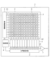
- FIG. 1 is a schematic configuration diagram showing the entire solid-state image sensor 1 according to the first embodiment of the present disclosure.
- the solid-state image sensor 1 shown in FIG. 1 is a back-illuminated CMOS (Complementary Metal Oxide Semiconductor) image sensor. As shown in FIG. 18, the solid-state image sensor 1 captures image light (incident light 1006) from the subject through the optical lens 1002, and transmits the amount of light of the incident light 1006 imaged on the imaging surface to a signal processing circuit. In 1005, it is converted into an electric signal in pixel units and output as a video signal (pixel signal). As shown in FIG. 1, the solid-state image sensor 1 of the first embodiment includes a substrate 2, a pixel region 3, a vertical drive circuit 4, a column signal processing circuit 5, a horizontal drive circuit 6, and an output circuit 7. , The control circuit 8 is provided.
- CMOS Complementary Metal Oxide Semiconductor
- the pixel region 3 has a plurality of pixels 9 regularly arranged in a two-dimensional array on the substrate 2.
- the pixel 9 has a photoelectric conversion unit 23 shown in FIG. 2B and a plurality of pixel transistors (not shown).
- the plurality of pixel transistors for example, four transistors such as a transfer transistor, a reset transistor, a selection transistor, and an amplifier transistor can be adopted. Further, for example, three transistors excluding the selection transistor may be adopted.
- the vertical drive circuit 4 is composed of, for example, a shift register, selects a desired pixel drive wiring L1, supplies a pulse for driving the pixel 9 to the selected pixel drive wiring L1, and transfers each pixel 9 in rows. Drive. That is, the vertical drive circuit 4 selectively scans each pixel 9 in the pixel region 3 in a row-by-row manner in the vertical direction, and produces a pixel signal based on the signal charge generated by the photoelectric conversion unit 23 of each pixel 9 according to the amount of received light. , Supply to the column signal processing circuit 5 through the vertical signal line L2.
- the column signal processing circuit 5 is arranged for each column of the pixel 9, for example, and performs signal processing such as noise removal for each pixel string with respect to the signal output from the pixel 9 for one row.
- the column signal processing circuit 5 performs signal processing such as CDS (Correlated Double Sampling) and AD (Analog Digital) conversion for removing fixed pattern noise peculiar to pixels.
- the horizontal drive circuit 6 is composed of, for example, a shift register, sequentially outputs horizontal scanning pulses to the column signal processing circuit 5, selects each of the column signal processing circuits 5 in order, and from each of the column signal processing circuits 5.
- the signal-processed pixel signal is output to the horizontal signal line L3.
- the output circuit 7 processes and outputs the pixel signals sequentially supplied from each of the column signal processing circuits 5 through the horizontal signal line L3.
- the control circuit 8 obtains a clock signal or a control signal that serves as a reference for the operation of the vertical drive circuit 4, the column signal processing circuit 5, the horizontal drive circuit 6, etc., based on the vertical synchronization signal, the horizontal synchronization signal, and the master clock signal. Generate. Then, the control circuit 8 outputs the generated clock signal and control signal to the vertical drive circuit 4, the column signal processing circuit 5, the horizontal drive circuit 6, and the like.
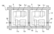
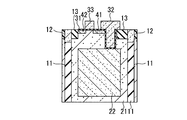
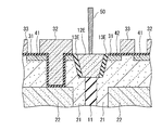
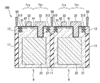
- FIG. 2A is a plan view showing an example of the layout of the solid-state image sensor 100 in the pixel region 3 of the solid-state image sensor 1.
- FIG. 2B is a cross-sectional view of the pixel 9 of the solid-state image sensor 100 in the AA'cross section shown in FIG. 2A.
- the solid-state image sensor 1 having the solid-state image sensor 100 shown in FIGS. 2A and 2B is a back-illuminated CMOS image sensor (CMOS type solid-state image sensor).
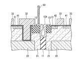
- the solid-state image sensor 100 includes a transfer transistor Ttr, a reset transistor Trs, an amplification transistor Tam, and a select transistor Tsl.
- the transfer transistor Ttr is a transistor that reads out the electric charge from the photoelectric conversion element 22 and transfers the electric charge to the floating diffusion 41.
- the reset transistor Trs is a transistor that resets the potential of the floating diffusion 41 to the power supply voltage.
- the amplification transistor Tam is a transistor that receives the potential of the floating diffusion 41 at the gate and outputs it to the vertical signal line (VSL) at the source follower.
- the select transistor Tsl is a transistor that connects the amplification transistor Tam of the read line and the vertical signal line, and disconnects the amplification transistor Tam of the line not read and the vertical signal line.
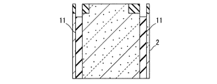
- the solid-state image sensor 100 is a completely penetrating element between pixels 9 (9a, 9b, etc.) including a photoelectric conversion element (PD: Photo Diode) 22 that photoelectrically converts incident light. It is a structure separated by separation (FFTI: Front Full Trench Isolation) 11.
- the solid-state image sensor 100 is photoelectric from the second main surface (lower surface in FIG. 2B) opposite to the first main surface (upper surface in FIG. 2B) which is the transistor forming surface of the solid-state image sensor 100. Light is incident on the conversion element 22.
- the first main surface may be referred to as an upper surface
- the second main surface may be referred to as a lower surface.
- the solid-state image sensor 100 includes a substrate 2, an FFTI 11, an embedded conductor portion 12, an insulating portion 13, a well layer 21, and a photoelectric conversion element 22. Further, the solid-state image sensor 100 includes a gate insulating film 31, gate electrodes 32, 33, 34 and 35, a floating diffusion 41 and a high-concentration impurity diffusion layer 42. Note that FIGS. 2A and 2B also show a GND contact 50 that is electrically connected to the embedded conductor portion 12. On the lower surface side of the substrate 2, a condensing layer in which a color filter layer and a wafer lens (not shown) are laminated in this order is formed. Further, a wiring layer and a logic substrate (not shown) are laminated in this order on the transistor forming side surface (upper surface) of the substrate 2.
- the substrate 2 is formed of, for example, silicon (Si).
- a pixel region 3 in which a plurality of pixels 9 are arranged is formed on the substrate 2.
- a plurality of pixels 9 including a photoelectric conversion element 22 are formed on the substrate 2 in the pixel region 3 and arranged in a two-dimensional matrix.
- the completely penetrating element separation (FFTI) 11 is formed so as to penetrate from the transistor forming side surface (upper surface) to the lower surface of the substrate 2 and completely separate each pixel 9.
- the FFTI 11 is provided so as to surround the pixel 9 in a plan view, and each pixel 9 is electrically separated from the adjacent pixel 9 by the FFTI 11.
- the FFTI 11 has a structure in which an element separation film such as a silicon oxide film or a silicon nitride film is embedded in a trench formed in the substrate 2. Further, the FFTI 11 may have a two-layer structure of an element separation membrane formed so as to cover the inner wall of the trench and a semiconductor film such as silicon embedded in the trench in which the element separation film is formed.
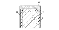
- the embedded conductor portion 12 functions as a contact electrode for GND contact with the substrate 2 (high-concentration impurity diffusion layer 42).
- the embedded conductor portion 12 can be embedded in a trench formed on the upper surface of the substrate 2.
- the embedded conductor portion 12 is formed by embedding all of the trenches provided in the upper part of the substrate 2 having the FFTI 11 as the bottom surface with a conductor film.
- each pixel 9 is electrically separated by the FFTI 11. Therefore, in the solid-state image sensor 100, each separated pixel 9 needs to have a potential (reference potential) contact of the well layer 21.
- a part of the FFTI 11 on the transistor forming surface side is used as an active region as an embedded conductor portion 12, and functions as a contact electrode.
- the embedded conductor portion 12 By arranging the embedded conductor portion 12 closely above the FFTI 11 in this way, it is possible to suppress an increase in the area of the solid-state image sensor 100 in a plan view due to the formation of the contact electrode, and solid-state imaging can be performed. The area of the element 100 can be reduced.
- the embedded conductor portion 12 is provided at all the boundaries between the pixels 9 as shown in FIG. 2A. Further, the GND contact 50 is provided so as to connect with a part of the embedded conductor portion 12 provided at the boundary between the pixels 9.
- the embedded conductor portion 12 is formed above the FFTI 11 (transistor forming surface side) in a cross-sectional view. Since the embedded conductor portion 12 is formed deeper than the insulating portion 13, the embedded conductor portion 12 is arranged in close contact with the well layer 21 in a region deeper than the insulating portion 13. As a result, the embedded conductor portion 12 is ohmic-bonded to the well layer 21 and electrically connected. As shown in FIGS. 2A and 2B, the embedded conductor portion 12 is provided in close contact with the FFTI 11 provided between the pixels 9, and is shared as a contact electrode for GND contact between two adjacent pixels 9. Will be done.
- the embedded conductor portion 12 is formed by a conductor film.
- silicon or other semiconductor material or metal doped with P-type or N-type impurities is preferably used.
- silicon for example, polycrystalline silicon, amorphous silicon, epitaxially grown silicon, and the like are preferable.
- the insulating portion 13 is an insulating layer provided between the embedded conductor portion 12 and the high-concentration impurity diffusion layer 42 on the upper surface (transistor forming side surface) of the substrate 2.
- the insulating portion 13 is formed by STI (Shallow Trench Isolation) or an insulating film.
- the STI may be any material that is generally used, and for example, silicon oxide is used.
- As the insulating film an oxide film is preferably used, and a silicon oxide film is particularly preferable.
- the insulating portion 13 is formed by embedding, for example, an oxide film as an insulating film in a trench formed on the upper surface (transistor forming side surface) of the substrate 2.
- the embedded conductor portion 12 and the high-concentration impurity diffusion layer 42 do not come into close contact with each other, and the distance between the embedded conductor portion 12 and the high-concentration impurity diffusion layer 42. Becomes larger. Therefore, a strong electric field is less likely to be generated between the embedded conductor portion 12 and the high-concentration impurity diffusion layer 42, and the stability of the output of the solid-state image sensor 100 is improved. Further, by providing such an insulating portion 13, the embedded conductor portion 12 and the high-concentration impurity diffusion layer 42 are separated from each other in the vertical direction (the depth direction of the substrate 2).
- the generation of a strong electric field between the embedded conductor portion 12 and the high-concentration impurity diffusion layer 42 is suppressed without increasing the size of the solid-state image sensor 100 in a plan view, and the solid-state image sensor 100 is small. It is possible to achieve both area reduction and improvement of output stability.
- the well layer 21 is a P-type region in which P-type (an example of the first conductive type) impurities are diffused at a low concentration.
- the well layer 21 is formed in a region deeper than the high-concentration impurity diffusion layer 42 described later.
- the well layer 21 is arranged in close contact with the conductor portion 12 in a region deeper than the insulating portion 13.
- the well layer 21 forms a PN junction with the photoelectric conversion element 22 as described later.
- the photoelectric conversion element 22 is a photodiode that converts incident light into an amount of electric charge corresponding to the amount of received light and stores it.
- the photoelectric conversion element 22 receives light corresponding to the color of the color filter incident on the lower surface of the substrate via a lens and a color filter arranged with respect to the photoelectric conversion element 22.
- the photoelectric conversion element 22 provided in each of the pixels 9 is separated by the FFTI 11.
- the photoelectric conversion element 22 is a region formed in a region surrounded by a well layer 21, which is a P-shaped region, in each pixel 9.
- the photoelectric conversion element 22 is an N-type region in which N-type (an example of a second conductive type) impurities different from the impurities diffused in the well layer 21 are diffused at a low concentration.
- the photoelectric conversion element 22 has a photoelectric conversion function by forming a PN junction with the well layer 21.
- the photoelectric conversion element 22 functions as a source region of the transfer transistor Ttr.
- the gate insulating film 31 is an insulating film formed between the photoelectric conversion element 22 and the floating diffusion 41, and between the floating diffusion 41 and the high-concentration impurity diffusion layer 42.
- the gate insulating film 31 is, for example, a silicon oxide film.
- the gate electrodes 32, 33, 34 and 35 are the gate electrodes of the transfer transistor Ttr, the reset transistor Trs, the amplification transistor Tam and the select transistor Tsl, respectively.
- the gate electrodes 32, 33, 34 and 35 are formed of a conductive film such as a polycrystalline silicon film.
- the gate electrode 32 is formed in a trench formed so as to extend to the vicinity of the photoelectric conversion element 22 with respect to the well layer 21.
- the gate electrode 32 is formed by embedding a conductive film in a trench provided with a gate insulating film 31 on the surface.
- the floating diffusion 41 is a region formed on the surface of the substrate 2 on the transistor forming side (upper side) and temporarily holding the electric charge read by the transfer transistor Ttr.
- the floating diffusion 41 is a region in which, for example, an N-type (an example of a second conductive type) impurities are diffused at a high concentration in a transistor-forming region on the upper surface of the substrate 2.
- the floating diffusion 41 is formed in a region of the well layer 21 including a boundary between the channel region of the transfer transistor Ttr and the channel region of the reset transistor Trs.
- the floating diffusion 41 functions as a drain region when the transfer transistor Ttr is driven, and functions as a source region when the reset transistor Trs is driven.
- the high-concentration impurity diffusion layer 42 is formed on the transistor forming surface (upper surface) side of the substrate 2, and is, for example, a region in which N-type (an example of the second conductive type) impurities are diffused at a high concentration.
- the high-concentration impurity diffusion layer 42 is formed shallower than the insulating portion 13.
- the high-concentration impurity diffusion layer 42 functions as a drain region of the reset transistor Trs.
- a strong electric field is generated between the embedded conductor portion 12 and the high-concentration impurity diffusion layer 42 without increasing the size of the solid-state image sensor 100 in a plan view. Can be suppressed, and the area of the solid-state image sensor 100 can be reduced and the output stability can be improved at the same time.
- FIGS. 3A to 3G are process cross-sectional views showing a method of manufacturing the solid-state image sensor 100.
- 3A to 3G show process sectional views of pixel 9 (unit pixel).
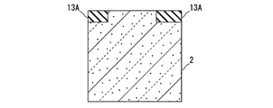
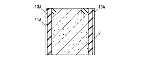
- the STI 13A is formed by forming a trench on the first main surface which is the transistor forming surface (upper surface in FIG. 3A) of the substrate 2 and embedding an insulating material.
- a silicon oxide film or silicon is formed.
- An element separation membrane 11' such as a nitride film is embedded. At this time, the trench is formed so as to penetrate the STI.
- a part of the first main surface of the element separation membrane 11'embedded in the trench is removed to form the trench.
- the FFTI 11 is formed by the element separation membrane 11'.
- An etching stopper film may be formed on the first main surface of the substrate 2 before removing a part of the first main surface of the element separation film 11'.
- a semiconductor film 12' such as polysilicon doped with impurities is formed so as to cover the formed trench and the first main surface of the substrate 2.
- the semiconductor film 12' is formed by, for example, a chemical vapor deposition (CVD) method or the like.
- the semiconductor film 12'deposited on the first main surface of the substrate 2 is flattened by chemical mechanical polishing (CMP).
- CMP chemical mechanical polishing
- the embedded conductor portion 12 is formed.
- a semiconductor element is formed in the pixels 9 separated by the FFTI 11.
- the well layer 21, which is a P-type region is formed by ion-implanting a P-type impurity into the substrate 2.
- the photoelectric conversion element 22 which is an N-type region is formed by ion-implanting an N-type impurity into the region surrounded by the well layer 21.
- a PN junction is formed between the well layer 21 and the photoelectric conversion element 22.
- the substrate 2 is subjected to thermal oxidation treatment to form a trench extending from the upper surface of the substrate 2 to the vicinity of the upper surface of the photoelectric conversion element 22.
- the gate insulating film 31 that covers the upper surface of the substrate 2 and the surface of the trench is formed.
- the conductive film is embedded in the trench provided with the gate insulating film 31, and the conductive film is formed on the upper surface of the substrate 2.
- a part of the conductive film is removed by using a lithography technique and an etching technique to form a gate electrode 32 of the transfer transistor Ttr and a gate electrode 33 of the reset transistor Trs.
- the ion-implanted region is activated by heat treatment.
- the floating diffusion 41 and the high-concentration impurity diffusion layer 42 are formed.
- an interlayer insulating film is formed so as to cover the upper surface of the substrate 2 on which each transistor is formed, and then a contact hole is formed which penetrates the interlayer insulating film and leads to the embedded conductor portion 12. Finally, the GND contact 50 is formed by embedding a conductive material in the contact hole. In FIG. 3G, the interlayer insulating film is not shown, and only the GND contact 50 is shown.
- the solid-state image sensor 100A to 100G is different from the solid-state image sensor 100 according to the first embodiment in that the embedded conductor portions 12A to 12G are provided in place of the embedded conductor portion 12.
- the portion having the same function as the solid-state image pickup device 100 according to the first embodiment will not be described in detail and shown in FIGS. 4 to 9. That is, the FFTI 11, the insulating portion 13, the well layer 21, the photoelectric conversion element 22, the gate insulating film 31, the gate electrodes 32, 33, 34 and 35, and the floating diffusion 41 formed in the pixels 9 of the solid-state image sensors 100A to 100G.
- the detailed description of the high-concentration impurity diffusion layer 42 and the high-concentration impurity diffusion layer 42 will be omitted.
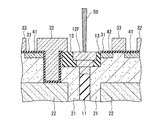
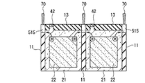
- FIG. 4 is a cross-sectional view of the pixel 9 of the solid-state image sensor 100A, which is an example of a modified example of the solid-state image sensor 100.
- FIG. 4 is a cross-sectional view corresponding to FIG. 2B in the first embodiment.
- the embedded conductor portion 12A of the solid-state imaging device 100A is a conductor film formed on the surface of a trench provided on the upper portion of the substrate 2 having the FFTI 11 as the bottom surface.
- the embedded conductor portion 12A may have a portion that is in close contact with the well layer 21. That is, the embedded conductor portion 12A may have a shape in which a part of the trench is embedded by the conductor material (the conductor material does not completely embed the trench).
- the embedded conductor portion 12B is a conductive film formed on the surface of a trench formed on the upper surface of the substrate 2, and the trench is surrounded laterally and downwardly by the conductive film. There is an air layer.
- the embedded conductor portion 12B may have a structure in which pure polysilicon or an oxide film is embedded in the trench.
- FIG. 5 is a cross-sectional view of the pixel 9 of the solid-state image sensor 100B, which is an example of a modified example of the solid-state image sensor 100.
- FIG. 5 is a cross-sectional view corresponding to FIG. 2B in the first embodiment.
- the embedded conductor portion 12B of the solid-state imaging device 100B is a conductor film formed on the surface of a trench provided on the upper portion of the substrate 2 having the FFTI 11 as the bottom surface.
- the embedded conductor portion 12B may have a portion that is in close contact with the well layer 21.
- the embedded conductor portion 12A may have a shape in which a part of the trench is embedded by the conductor material (the conductor material does not completely embed the trench). That is, the embedded conductor portions 12A and 12B may have a shape in which the conductor material does not completely embed the trench.
- the embedded conductor portion 12B is a conductive film formed on the surface of a trench formed on the upper surface of the substrate 2, and the trench is surrounded laterally and downwardly by the conductive film. There is an air layer.
- the embedded conductor portion 12B may have a structure in which pure polysilicon or an oxide film is embedded in the trench.
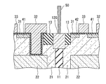
- FIGS. 6A and 6B are cross-sectional views of pixels 9 of the solid-state image sensor 100C, which is an example of a modified example of the solid-state image sensor 100.
- 6A and 6B are cross-sectional views corresponding to FIG. 2B in the first embodiment.
- the embedded conductor portions 12C and 12D of the solid-state imaging device 100C are embedded in a trench formed near the upper surface of the substrate 2 having the FFTI 11 as the bottom surface.
- the embedded conductor portions 12C and 12D have an inverted tapered shape or a tapered shape in a cross-sectional view.
- FIG. 6A illustrates a configuration in which the embedded conductor portion 12C has a tapered shape in which the width decreases from the lower surface to the upper surface of the embedded conductor portion 12C.
- FIG. 6B illustrates a configuration in which the embedded conductor portion 12D has a tapered shape in which the width decreases from the upper surface to the lower surface of the embedded conductor portion 12C.
- a trench for forming the FFTI 11 and the embedded conductor portions 12C and 12D is formed so as to penetrate the STI formed on the upper surface of the substrate 2, and the inside of the trench is formed.
- An insulating film is embedded in the FFTI 11 to form the FFTI 11.
- the embedded conductor portions 12C and 12D are formed by embedding a conductor film in the upper part of the FFTI 11 in the trench.
- the shape of the trench may be tapered, and the cross-sectional shape of the embedded conductor portions 12C and 12D is also tapered.
- FIG. 7 is a cross-sectional view of the pixel 9 of the solid-state image sensor 100D, which is an example of a modified example of the solid-state image sensor 100.
- FIG. 7 is a cross-sectional view corresponding to FIG. 2B in the first embodiment.
- the embedded conductor portion 12E and the insulating portion 13E of the solid-state image sensor 100D each have a tapered shape in which the width narrows from the lower surface to the upper surface in a cross-sectional view.
- the embedded conductor portion 12E In order to form the embedded conductor portion 12E, first, for example, a trench is formed on the upper surface of the substrate 2 to form an STI to be the insulating portion 13. Subsequently, a trench for forming the FFTI 11 and the embedded conductor portion 12E is formed so as to penetrate the STI, and an insulating film is embedded in the trench to form the FFTI 11. Finally, the embedded conductor portion 12E is formed by embedding a conductor film in the upper part of the FFTI 11 in the trench. Depending on the process such as etching at the time of forming the embedded conductor portion 12E, the shape of the trench formed when the insulating portion 13 is formed and the shape of the trench formed when the embedded conductor portion 12E is formed are both. It may have a tapered shape. In such a case, the cross-sectional shapes of the insulating portion 13 and the embedded conductor portion 12E are similarly tapered.
- FIG. 8 is a cross-sectional view of pixels 9 of the solid-state image sensor 100E, which is an example of a modification of the solid-state image sensor 100.
- FIG. 8 is a cross-sectional view corresponding to FIG. 2B in the first embodiment.
- the embedded conductor portion 12F of the solid-state imaging device 100E is embedded in a trench formed near the upper surface of the substrate 2 having the FFTI 11 as the bottom surface.
- the embedded conductor portion 12F has a shape in which a plurality of cylinders whose diameters gradually increase toward the upper surface of the substrate 2 are laminated in a cross-sectional view.
- the embedded conductor portion 12F In order to form the embedded conductor portion 12F, first, a trench for forming the FFTI 11 and the embedded conductor portion 12F is formed so as to penetrate the STI formed on the upper surface of the substrate 2, and an insulating film is formed in the trench. It is embedded to form FFTI11. Subsequently, the embedded conductor portion 12F is formed by embedding a conductor film in the upper part of the FFTI 11 in the trench. At this time, by forming the trench for forming the FFTI 11 and the embedded conductor portion 12F by etching a plurality of times, the shape of the trench may be a shape in which a plurality of cylinders are stacked. In this case, the cross-sectional shape of the embedded conductor portion 12F is also a shape in which a plurality of cylinders are stacked.
- FIG. 9 is a cross-sectional view of the pixel 9 of the solid-state image sensor 100F, which is an example of a modification of the solid-state image sensor 100.
- FIG. 9 is a cross-sectional view corresponding to FIG. 2B in the first embodiment.
- the embedded conductor portion 12G of the solid-state imaging device 100F is embedded in a trench formed near the upper surface of the substrate 2 having the FFTI 11 as the bottom surface.
- the embedded conductor portion 12G has a wider width than the FFTI 11 in cross-sectional view.
- the width of the trench of the embedded conductor portion 12G forming portion may be wider than the width of the trench of the FFTI 11 forming portion.
- the embedded conductor portion 12G has a wider width than the FFTI 11 in cross-sectional view.
- the solid-state image sensor 1, the solid-state image sensor 100, and the solid-state image sensor 100A to 100G according to the present embodiment have the following effects.
- an embedded conductor portion 12 that functions as a contact electrode is provided in close contact with the completely penetrating element separation (FFTI) 11 that separates each pixel 9.
- FFTI completely penetrating element separation
- an insulating portion 13 is provided between the embedded conductor portion 12 and the high-concentration impurity diffusion layer 42 in a plan view.
- the embedded conductor portion 12 formed deeper than the insulating portion 13 and the high density formed shallower than the insulating portion 13 near the surface of the transistor forming surface of the substrate 2.
- An insulating portion 13 is provided between the impurity diffusion layer 42 and the impurity diffusion layer 42.
- the embedded conductor portion 12 and the high-concentration impurity diffusion layer 42 are separated from each other in the vertical direction (the depth direction of the substrate 2). Therefore, the generation of a strong electric field between the embedded conductor portion 12 and the high-concentration impurity diffusion layer 42 is suppressed without increasing the size of the solid-state image sensor 100 in a plan view, and the solid-state image sensor 100 is small. It is possible to achieve both area reduction and improvement of output stability.
- Solid-state image pickup device 200 The solid-state image pickup device 200 according to the second embodiment of the present disclosure will be described.
- the solid-state image sensor 200 is a solid-state image sensor that can be used in place of the solid-state image sensor 100 of the solid-state image sensor 1 described in the first embodiment.
- the solid-state image pickup devices 200A, 200B, and 200C which are three examples of the solid-state image pickup device 200, will be described with reference to FIGS. 10 to 12.
- a portion having the same function as the solid-state image sensor 100 according to the first embodiment will not be described in detail and shown in FIGS. 10 to 12.
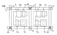
- FIG. 10 is a plan view showing an example of the layout of the solid-state image sensor 200A, which is an example of the solid-state image sensor 200.
- the solid-state image sensor 200A has the first embodiment in that the embedded conductor portion 12 is provided in close contact with a part of the surface of the FFTI 11 provided at the boundary between the pixels 9. It is different from the solid-state image sensor 100 according to the above.
- the arrangement of the FFTI 11 and the embedded conductor portion 12 and the connection of the GND contact 50 will be described.
- the FFTI 11 of the solid-state image sensor 200A is provided at all the boundaries between the pixels 9. Further, the embedded conductor portion 12 of the solid-state image sensor 200A separates four FFTI 11s that separate adjacent pixels 9 from a part of the boundary between the pixels 9, particularly four pixels 9 arranged in 2 ⁇ 2. Is provided only at the intersection of (the central portion of the four pixels 9). That is, the embedded conductor portions 12 of the solid-state image sensor 200A are provided at the four corners of one pixel 9.
- an embedded conductor portion 12 is provided adjacent to the upper side of the FFTI 11 (the front side in FIG. 10).
- the embedded conductor portion 12 is formed closer to the well layer 21 by being formed deeper than the insulating portion 13.
- the embedded conductor portion 12 is not provided above the FFTI 11 (front side in FIG. 10), and the transistor forming side surface of the substrate 2 (front side surface in FIG. 10) is not provided.
- the FFTI 11 is provided to the lower surface (the inner side surface in FIG. 10).
- the embedded conductor portion 12 When the embedded conductor portion 12 is provided above a part of the FFTI 11 (four corners of one pixel 9), the embedded conductor portion 12 removes the upper part of the embedded semiconductor material after embedding the semiconductor material, for example, oxidation.
- the upper part may be covered with an insulator such as silicon and sealed.
- the embedded conductor portion 12 is shared as a contact electrode for GND contact between four adjacent pixels 9. Pixel 9 will have four contact electrodes at each of the four corners. Therefore, in the solid-state image sensor 200A, even if any of the embedded conductor portions 12 does not function as a contact electrode, the other embedded conductor portion 12 functions as a contact electrode, and the solid-state image sensor 200A is used. The quality of the solid-state image sensor 1 to be provided is improved.
- FIG. 11 is a plan view showing an example of the layout of the solid-state image sensor 200B, which is an example of the solid-state image sensor 200.
- the solid-state image sensor 200B has the first embodiment in that the embedded conductor portion 12 is provided in close contact with a part of the surface of the FFTI 11 provided at the boundary between the pixels 9. It is different from the solid-state image sensor 100 according to the above.
- the GND contact 50 is connected to a part of the formed embedded conductor portion 12, and only a part of the embedded conductor portion 12 functions as a contact electrode. It is different from the solid-state image sensor 200A.
- the arrangement of the FFTI 11 and the embedded conductor portion 12 and the connection of the GND contact 50 will be described.
- the FFTI 11 of the solid-state image sensor 200B is provided at all the boundaries between the pixels 9. Further, the embedded conductor portion 12 of the solid-state image sensor 200B is a part of the boundary between the pixels 9, particularly the four FFTI 11s that separate the adjacent pixels 9 out of the four pixels 9 arranged in 2 ⁇ 2. Is provided only at the intersection of (the central portion of the four pixels 9). That is, the embedded conductor portions 12 of the solid-state image sensor 200B are provided at the four corners of one pixel 9.
- an embedded conductor portion 12 formed above the FFTI 11 (front side in FIG. 11) is provided deeper than the insulating portion 13 and in contact with the well layer 21. There is.
- the GND contact 50 is connected to a part of the embedded conductor portion 12 provided at the intersection of the four FFTI 11.
- the GND contact 50 may be electrically connected to the adjacent pixel 9. Therefore, for example, as shown in FIG. 11, the GND contact 50 may be connected to a pair of embedded conductor portions 12 provided at diagonal positions in one pixel 9.
- the embedded conductor portion 12 arranged as described above is shared as a contact electrode for GND contact between four adjacent pixels 9.
- the pixel 9 will have two contact electrodes at its two corners. Therefore, in the solid-state image sensor 200B, even if one embedded conductor portion 12 does not function as a contact electrode, the other embedded conductor portion 12 functions as a contact electrode and has the solid-state image sensor 200B. The quality of the solid-state image sensor 1 is improved.
- FIG. 12 is a plan view showing an example of the layout of the solid-state image sensor 200C, which is an example of the solid-state image sensor 200.
- the solid-state image sensor 200C has the first embodiment in that the embedded conductor portion 12 is provided in close contact with a part of the surface of the FFTI 11 provided at the boundary between the pixels 9. It is different from the solid-state image sensor 100 according to the above. Further, the solid-state image sensor 200C is different from the solid-state image sensor 200A in that the embedded conductor portion 12 is provided only at diagonal positions (two corners) of one pixel 9.
- the arrangement of the FFTI 11 and the embedded conductor portion 12 and the connection of the GND contact 50 will be described.
- the FFTI 11 of the solid-state image sensor 200C is provided at all the boundaries between the pixels 9. Further, the embedded conductor portion 12 of the solid-state image sensor 200C is provided at a part of the boundary between the pixels 9. The embedded conductor portion 12 is provided at a pair of diagonal positions of one pixel 9.
- an embedded conductor portion 12 formed deeper than the insulating portion 13 and in contact with the well layer 21 is provided. Has been done.
- the GND contact 50 is connected to each of the embedded conductor portions 12 provided diagonally to the pixel 9.
- the embedded conductor portion 12 arranged as described above is shared as a contact electrode for GND contact between four adjacent pixels 9.
- the pixel 9 will have two contact electrodes at its two corners. Therefore, in the solid-state image sensor 200C, even if one embedded conductor portion 12 does not function as a contact electrode, the other embedded conductor portion 12 functions as a contact electrode and has the solid-state image sensor 200C. The quality of the solid-state image sensor 1 is improved. Further, by not providing the embedded conductor portion 12 in the portion where the GND contact 50 is not arranged, such as the solid-state image sensor 200C, the characteristics of the solid-state image sensor 200C and the yield at the time of manufacturing the solid-state image sensor 200C are increased.
- the solid-state imaging device 200 may have any of the embedded conductor portions 12A to 12G of the modified example of the first embodiment instead of the embedded conductor portion 12.
- the solid-state image sensor 200 has the following effects in addition to the effects described in the first embodiment.
- an embedded conductor portion 12 that functions as a contact electrode is provided at a corner portion of each pixel 9.
- the embedded conductor portion 12 is shared as a contact electrode for GND contact between the four adjacent pixels 9, and even if any of the embedded conductor portions 12 does not function as a contact electrode, the other The embedded conductor portion 12 of the above functions as a contact electrode. Therefore, the quality of the solid-state image sensor 1 having the solid-state image sensor 200A is improved.
- the embedded conductor portion 12 is provided only at the diagonal corners (two corners) of each pixel 9. As a result, the characteristics of the solid-state image sensor 200C and the yield at the time of manufacturing the solid-state image sensor 200C are improved as compared with the case where the embedded conductor portions 12 are provided at the four corners of each pixel 9.
- the solid-state image sensor 300 is a solid-state image sensor that can be used in place of the solid-state image sensor 100 of the solid-state image sensor 1 described in the first embodiment.
- the solid-state image sensor 300 will be described with reference to FIG.
- the portion of the solid-state image sensor 300 that has the same function as the solid-state image sensor 100 according to the first embodiment will not be described in detail and shown in FIG. That is, the well layer 21, the photoelectric conversion element 22, the gate insulating film 31, the gate electrodes 32, 33, 34 and 35, the floating diffusion 41 and the high-concentration impurity diffusion layer 42 formed in the pixel 9 of the solid-state image sensor 300. Will omit detailed description and illustration.
- FIG. 13 is a cross-sectional view of the pixel 9 of the solid-state image sensor 300.
- FIG. 13 is a cross-sectional view corresponding to FIG. 2B in the first embodiment.
- the solid-state image sensor 300 is different from the solid-state image sensor 100 according to the first embodiment in that it includes an insulating portion 313 instead of the insulating portion 13.
- the insulating portion 313 includes an insulating film covering the surface of the trench provided between the embedded conductor portion 12 and the high-concentration impurity diffusion layer 42, and pure polysilicon or pure polysilicon embedded in the trench. It has a two-layer structure with oxides. Further, the insulating portion 313 may be provided with an air layer (air gap) instead of pure polysilicon or oxide.
- the surface of the insulating portion 313 may be formed of an insulating material.
- the width of the insulating portion 313 can be narrowed as compared with the insulating portion 13, which is effective for miniaturization of pixels.
- the solid-state imaging device 300 may have any of the embedded conductor portions 12A to 12G of the modified example of the first embodiment instead of the embedded conductor portion 12.
- the solid-state image sensor 300 has the following effects in addition to the effects described in the first embodiment.
- the insulating portion 313 has two layers, that is, an insulating film formed on the surface of the trench, pure polysilicon or an oxide film embedded in the trench in which the insulating film is formed, or an air layer. It is said to be a structure. As a result, the width of the insulating portion 313 can be formed to be narrower, which is further effective in reducing the area of the solid-state image sensor 300.
- Solid-state image pickup device 400 The solid-state image pickup device 400 according to the fourth embodiment of the present disclosure will be described.
- the solid-state image sensor 400 is a solid-state image sensor that can be used in place of the solid-state image sensor 100 of the solid-state image sensor 1 described in the first embodiment.
- the solid-state image sensor 400 will be described with reference to FIGS. 14A to 14C.
- the solid-state image sensor 400 is different from the solid-state image sensor 100 according to the first embodiment in that it includes an embedded conductor portion 412 for connecting between pixels 9 instead of the embedded conductor portion 12. Further, the solid-state image sensor 400 is different from the solid-state image sensor 100 according to the first embodiment in that it includes an insulating portion 414. Further, the solid-state image sensor 400 is different from the solid-state image sensor 100 according to the first embodiment in that the contact electrode 460 and the embedded conductor portion 43 are provided.
- the portion having the same function as the solid-state image sensor 100 according to the first embodiment is omitted in detail and not shown in FIGS. 14A to 14C. That is, the FFTI 11, the insulating portion 13, the well layer 21, the photoelectric conversion element 22, the gate insulating film 31, the gate electrodes 32, 33, 34 and 35, and the floating diffusion 41 and the height formed in the pixel 9 of the solid-state image sensor 400.
- a detailed description of the concentration impurity diffusion layer 42 will be omitted.
- FIG. 14A is a plan view showing an example of the layout of the solid-state image sensor 400.
- FIG. 14B is a cross-sectional view of the pixel 9 of the solid-state image sensor 400 in the BB'cross section shown in FIG. 14A.
- FIG. 14B is a cross-sectional view of a portion including the transfer transistor Ttr and the reset transistor Trs.
- FIG. 14C is a cross-sectional view of the pixel 9 of the solid-state image sensor 400 in the CC'cross section shown in FIG. 14A.
- FIG. 14C is a cross-sectional view of a portion including the amplification transistor Tam and the select transistor Tsl.
- the solid-state image sensor 400 has a contact electrode 460 in the pixel 9. Further, as shown in FIGS. 14B and 14C, the solid-state imaging device 400 has an embedded conductor portion 412 provided on the upper portion of the FFTI 11 and an insulating portion 414 provided on the upper portion of the embedded conductor portion 412. ing.
- the embedded conductor portion 412 is provided between the FFTI 11 and the insulating portion 414.
- the embedded conductor portion 412 is formed to a position deeper than the insulating portion 13 of the substrate 2, and is arranged in close contact with the well layers 21 of both adjacent pixels 9. That is, the embedded conductor portion 412 has a function of electrically connecting each pixel 9.
- the embedded conductor portion 412 of the present embodiment does not have a function as a contact electrode.
- the embedded conductor portion 412 is formed of the same material as the embedded conductor portion 12.
- the embedded conductor portion 412 is formed by embedding a conductor film in the upper part of the FFTI 11 and then removing the upper part of the embedded conductor.
- the insulating portion 414 is provided above the embedded conductor portion 412 and has a function as a cap layer of the insulating portion 414.
- the insulating portion 414 is formed of, for example, silicon oxide or silicon nitride, or other insulating portion.
- the insulating portion 414 is formed by embedding the insulating portion in the upper part of the embedded conductor portion 412 in the trench.
- the contact electrode 460 is a region for connecting to and making contact with the GND contact 50. As shown in FIG. 14C, the contact electrode 460 is connected to the well layer 21 and fixes the well layer 21 to the potential input from the GND contact 50.
- the contact electrode 460 is formed in the pixel 9 region. Further, the contact electrode 460 may be arranged inside the pixel 9 region and outside the pixel 9 region (outside the pixel region 3 shown in FIG. 1). When the contact electrode 460 is formed in the pixel 9 region, one contact electrode 460 is provided for each of several pixels 9. In this case, the pixel 9 provided with the contact electrode 460 is preferably the pixel 9 provided with the blue (B) color filter.
- the contact electrode 460 is provided in the pixel 9 provided with the blue (B) color filter, it is possible to suppress the variation in the output between the pixels 9 and improve the uniformity of the output from each pixel 9. it can.
- Pixels 9 are electrically connected by an embedded conductor portion 412. Therefore, one contact electrode 460 functions as a potential (reference potential) contact of the well layer 21 of each pixel 9 separated.
- Pixel 9 is a region where impurities are diffused at a high concentration, in which the contact electrode 460 is provided to make contact with the GND contact 50.
- the contact electrode 460 is formed at a depth at which the lower surface is in electrical contact with the well layer 21.
- the contact electrode 460 is formed by embedding a conductor film in a trench provided on the substrate 2.
- silicon or other semiconductor material or metal doped with P-type impurities is preferably used.
- the silicon for example, polycrystalline silicon, amorphous silicon, epitaxially grown silicon, and the like are preferable.
- the solid-state image sensor 400 has the following effects. (7)
- each pixel 9 is electrically connected by an embedded conductor portion 412, and a contact electrode 460 is provided in one of several pixels 9.
- the number of contact electrodes 460 is reduced as compared with the case where the contact electrodes 460 are provided for each pixel 9, which is effective in reducing the area of the solid-state image sensor 300.
- a blue (B) color filter may be provided, and a contact electrode 460 may be provided on the pixel 9 on which blue light having a short wavelength is incident. In this case, it is possible to suppress the variation in the output between the pixels 9 depending on the presence or absence of the contact electrode 460, and improve the uniformity of the output from each pixel 9.
- the solid-state image sensor 500 is a solid-state image sensor that can be used in place of the solid-state image sensor 100 of the solid-state image sensor 1 described in the first embodiment.
- the solid-state image sensor 500 will be described with reference to FIGS. 15A to 15C.
- the solid-state image sensor 500 has the first embodiment in that the embedded conductor portion 512 is provided in close contact with a part of the surface of the FFTI 11 provided at the boundary between the pixels 9. It is different from the solid-state image sensor 100 according to the above.
- the solid-state image sensor 500 includes an embedded conductor portion 512 in each region including the four corners of one pixel 9 in a plan view. Further, the solid-state image sensor 500 is different from the solid-state image sensor 100 according to the first embodiment in that it includes an embedded conductor portion 515 provided on the boundary between the two pixels 9.
- the portion having the same function as the solid-state image sensor 100 according to the first embodiment will not be described in detail and shown in FIGS. 15A to 15C. That is, the FFTI 11, the insulating portion 13, the well layer 21, the photoelectric conversion element 22, the gate insulating film 31, the gate electrodes 32, 33, 34 and 35, and the floating diffusion 41 and the height formed in the pixel 9 of the solid-state image sensor 500. A detailed description of the concentration impurity diffusion layer 42 will be omitted.
- FIG. 15A is a plan view showing an example of the layout of the solid-state image sensor 500.
- FIG. 15B is a cross-sectional view of the pixel 9 of the solid-state image sensor 500 in the DD'cross section shown in FIG. 2A.
- FIG. 15B is a cross-sectional view of a region including an embedded conductor portion 515 having an electron trap function.
- FIG. 15C is a cross-sectional view of the pixel 9 of the solid-state image sensor 500 in the EE cross section shown in FIG. 2A.
- FIG. 15C is a cross-sectional view of a region including an embedded conductor portion 512 that functions as a contact electrode.
- the embedded conductor portions 512 provided at the four corners of the pixel 9 function as contact electrodes for fixing the potential of the well layer 21, similarly to the embedded conductor portion 12 in the first embodiment.
- the FFTI 11 of the solid-state image sensor 500 is provided at all the boundaries between the pixels 9. Further, the embedded conductor portion 512 of the solid-state image sensor 500 separates the adjacent pixels 9 from a part of the boundary between the pixels 9, particularly the four pixels 9 arranged in 2 ⁇ 2, four FFTI 11s. Is provided in the region including the intersecting portion (the central portion of the four pixels 9). That is, the embedded conductor portions 512 of the solid-state image sensor 500 are provided at the four corners of one pixel 9. As shown in FIG.
- the embedded conductor portion 512 is provided above the FFTI 11 (upper side of FIG. 15B) in the region including the four corners of the pixel 9 so as to be deeper than the insulating portion 13 and in contact with the well layer 21. ing.
- FIG. 15A as an example, the cross-shaped embedded conductor portion 512 in a plan view is shown.
- the embedded conductor portion 512 is formed by the same material and manufacturing method as the embedded conductor portion 12 of the first embodiment.
- the embedded conductor portion 515 provided on the boundary between the pixels 9 has an electron trap function for suppressing charge overflow to the adjacent pixel 9 via the embedded conductor portion 512 or 515 when the amount of light is large.
- the embedded conductor portion 515 is provided above a part of the FFTI 11 (upper side in FIG. 15B) located at the boundary between the pixels 9 so as to be deeper than the insulating portion 13 and in contact with the well layer 21.
- silicon or other semiconductor material or metal doped with N-type impurities is preferably used.
- the silicon for example, polycrystalline silicon, amorphous silicon, epitaxially grown silicon, and the like are preferable.
- the embedded conductor portion 512 is electrically connected to the GND contact 50. As a result, the embedded conductor portion 512 functions as a contact electrode.
- the embedded conductor portion 512 is shared as a contact electrode for GND contact between four adjacent pixels 9. Pixel 9 will have four contact electrodes at each of the four corners. Therefore, in the solid-state image sensor 500, even if any of the embedded conductor portions 512 does not function as a contact electrode, the other embedded conductor portion 512 functions as a contact electrode, and the solid-state image sensor 500 is used. The quality of the solid-state image sensor 1 to be provided is improved.
- the embedded conductor portion 515 is electrically connected to the VDD contact 570 that applies a positive voltage to the embedded conductor portion 515.
- the embedded conductor portion 515 is formed of, for example, an N-type semiconductor material, and traps electrons accumulated in the photoelectric conversion element 22 when a positive voltage is applied. As a result, even when the electrons accumulated in the photoelectric conversion element 22 are likely to overflow to the adjacent pixels due to the large amount of light, the electrons can be prevented from flowing to the adjacent pixels 9. As a result, the solid-state image sensor 500 can suppress color mixing between adjacent pixels 9 in which color filters of different colors are arranged.
- the solid-state image sensor 500 it is preferable to make a difference in the strength between the barrier from the photoelectric conversion element 22 to the embedded conductor portion 515 and the barrier from the photoelectric conversion element 22 to each transistor such as the transfer transistor Ttr. As a result, it is possible to prevent the electrons overflowing from the photoelectric conversion element 22 from affecting each transistor when the amount of light is large.
- the solid-state imaging device 500 may have any of the embedded conductor portions 12A to 12G of the modified example of the first embodiment instead of the embedded conductor portion 512. Further, in the solid-state image sensor 500, the embedded conductor portion 515 may have the same configuration as the embedded conductor portions 12A to 12G of the modified example of the first embodiment. Further, the solid-state image sensor 500 may have the insulating portion 313 of the third embodiment instead of the insulating portion 13.
- the solid-state image sensor 500 has the following effects in addition to the effects described in the first embodiment.
- the solid-state image sensor 500 includes an embedded conductor portion 515 that is electrically connected to the VDD contact and traps electrons overflowing from the photoelectric conversion element 22 when a positive voltage is applied from the VDD contact. .. Therefore, it is possible to suppress the electrons overflowing from the photoelectric conversion element 22 from flowing to the adjacent pixels 9 at the time of a large amount of light, and to suppress the color mixing with the adjacent pixels 9.
- the solid-state image sensor 600 is a solid-state image sensor that can be used in place of the solid-state image sensor 100 of the solid-state image sensor 1 described in the first embodiment.
- the solid-state image pickup devices 600A and 600B which are two examples of the solid-state image pickup device 600, will be described with reference to FIGS. 16 and 17.
- the solid-state image sensor 600 a portion having the same function as the solid-state image sensor 100 according to the first embodiment will not be described in detail and shown in FIGS. 16 and 17. That is, the FFTI 11, the insulating portion 13, the well layer 21, the photoelectric conversion element 22, the gate insulating film 31, the gate electrodes 32, 33, 34 and 35, and the floating diffusion 41 formed in the pixels 9 of the solid-state image sensors 600A and 600B.
- the detailed description of the high-concentration impurity diffusion layer 42 and the high-concentration impurity diffusion layer 42 will be omitted.
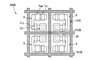
- FIG. 16 is a plan view showing an example of the layout of the solid-state image sensor 600A, which is an example of the solid-state image sensor 600.
- the solid-state imaging device 600A includes an embedded conductor portion 612A provided in a part of a region on the boundary sandwiched between the two pixels 9 instead of the embedded conductor portion 12. It differs from the solid-state image sensor 100 according to the first embodiment in that. Further, the solid-state image sensor 600A is different from the solid-state image sensor 100 according to the first embodiment in that the embedded conductor portion 615A is provided in a region excluding the region where the embedded conductor portion 612A is formed on the FFTI 11 surrounding each pixel. It's different.
- the arrangement of the FFTI 11, the embedded conductor portion 612A and the embedded conductor portion 615A, and the connection of the GND contact 50 will be described.
- the solid-state image sensor 600A is a solid-state image sensor in which two adjacent pixels 9 are used as pixel sharing units.
- One embedded conductor portion 612A is provided for two adjacent pixels 9.
- the embedded conductor portion 612A is provided on the upper portion (front side in FIG. 16) of the FFTI 11 (not shown) provided at the boundary between two adjacent pixels 9.
- the embedded conductor portion 612A is provided near the center of the FFTI 11 sandwiched between the two pixels 9 in a plan view.
- the upper surface of the embedded conductor portion 612A is exposed from the embedded conductor portion 615A described later, and the GND contact 50 is connected to the embedded conductor portion 612A.
- the embedded conductor portion 612A functions as a contact electrode in the same manner as the embedded conductor portion 12 described in the first embodiment.
- the embedded conductor portion 612A is formed in the same manner as the embedded conductor portion 12 except that the embedded conductor portion 612A is provided on a part of the FFTI 11 provided at the boundary between two adjacent pixels 9.
- the embedded conductor portion 615A is provided above the FFTI 11 (not shown) provided at the boundary of each pixel 9.
- the embedded conductor portion 615A is formed in a region excluding the region on which the embedded conductor portion 612A is formed on the FFTI 11. Similar to the embedded conductor portion 515 described in the fifth embodiment, the embedded conductor portion 615A is for suppressing the overflow of electric charge to the adjacent pixel 9 via the embedded conductor portion 612A or 615A when the amount of light is large. It has an electronic trap function.
- the embedded conductor portion 615A is formed in the same manner as the embedded conductor portion 515 except that it is provided in a region surrounding most of each pixel 9.
- a VDD contact 670 that applies a positive voltage to the embedded conductor portion 615A is connected to the embedded conductor portion 615A.
- the VDD contact 670 is formed of the same material and method as the VDD contact 570 of the fifth embodiment.
- the embedded conductor portion 612A as a GND marriage electrode is shared by each pixel sharing unit composed of two pixels 9.
- a high-intensity light source is incident on the solid-state image sensor 600A and electrons overflow from the pixel 9 via the embedded conductor portion 612A, electrons are emitted to other pixels 9 in the shared pixel unit via the embedded conductor portion 612A.
- it flows in it is possible to suppress the inflow of electrons into other pixels 9 outside the shared pixel unit. Therefore, deterioration of image quality can be suppressed by the same processing as pixel correction due to defects in the shared pixel unit.
- FIG. 17 is a plan view showing an example of the layout of the solid-state image sensor 600B, which is an example of the solid-state image sensor 600.
- the solid-state imaging device 600B includes an embedded conductor portion 612B provided in a region on the boundary surrounded by the four pixels 9 instead of the embedded conductor portion 12. It is different from the solid-state image sensor 100 according to the first embodiment.
- the solid-state image sensor 600A is different from the solid-state image sensor 100 according to the first embodiment in that the embedded conductor portion 615B is provided in a region excluding the region where the embedded conductor portion 612A is formed on the FFTI 11 surrounding each pixel. It's different.
- the arrangement of the FFTI 11, the embedded conductor portion 612B and the embedded conductor portion 615B, and the connection of the GND contact 50 will be described.
- the solid-state image sensor 600B is a solid-state image sensor in which four pixels 9 arranged in a 2 ⁇ 2 matrix are used as pixel sharing units.
- One embedded conductor portion 612B is provided for each of the four pixels 9 arranged in a matrix.
- the embedded conductor portion 612B is provided on the upper portion (front side in FIG. 17) of the FFTI 11 (not shown) located at the center of the four pixels 9.
- the upper surface of the embedded conductor portion 612B is exposed from the embedded conductor portion 615B described later, and the GND contact 50 is connected to the embedded conductor portion 612B.
- the embedded conductor portion 615B is provided above the FFTI 11 (not shown) provided at the boundary of each pixel 9.
- the embedded conductor portion 615B is formed in a region excluding the region on which the embedded conductor portion 612B is formed on the FFTI 11.
- the embedded conductor portion 615B has an electron trap function for suppressing the overflow of electrons to the adjacent pixel 9 via the embedded conductor portion 612B or 615B when the amount of light is large.
- the embedded conductor portion 615B is formed in the same manner as the embedded conductor portion 515 except that it is provided in a region surrounding most of each pixel 9.
- the embedded conductor portion 612B as a GND marriage electrode is shared by each pixel sharing unit composed of two pixels 9.
- a high-intensity light source is incident on the solid-state image sensor 600B and electrons overflow from the pixel 9 via the embedded conductor portion 612B, electrons are emitted to other pixels 9 in the shared pixel unit via the embedded conductor portion 612B.
- it flows in it is possible to suppress the inflow of electrons into other pixels 9 outside the shared pixel unit. Therefore, deterioration of image quality can be suppressed by the same processing as pixel correction due to defects in the shared pixel unit.
- the solid-state image sensor 600 has the following effects in addition to the effects described in the first embodiment.
- the solid-state image sensor 600 includes embedded conductor portions 615A and 615B that are electrically connected to the VDD contact and trap the electrons overflowing from the photoelectric conversion element 22 when a positive voltage is applied from the VDD contact. ing. Therefore, the solid-state image sensor 600 can suppress the electrons overflowing from the photoelectric conversion element 22 from flowing to the adjacent pixels 9 at the time of a large amount of light, and can suppress the color mixing with the adjacent pixels 9.
- the solid-state image sensor 600 can suppress the inflow of electrons into other pixels 9 outside the shared pixel unit even when electrons overflow from the pixel 9. Therefore, the solid-state image sensor 600 can suppress deterioration of image quality by the same processing as pixel correction due to defects in the shared pixel unit.
- FIG. 18 is a schematic configuration diagram of the electronic device 1000 according to the seventh embodiment of the present disclosure.
- the electronic device 1000 according to the seventh embodiment includes a solid-state imaging device 1, an optical lens 1002, a shutter device 1003, a drive circuit 1004, and a signal processing circuit 1005.
- the electronic device 1000 of the seventh embodiment shows an embodiment when the solid-state image sensor 1 according to the first embodiment of the present disclosure is used as the solid-state image sensor 1 in an electronic device (for example, a camera).
- the optical lens 1002 forms an image light (incident light 106) from the subject on the image pickup surface of the solid-state image sensor 1. As a result, the signal charge is accumulated in the solid-state image sensor 1 for a certain period of time.
- the shutter device 1003 controls the light irradiation period and the light blocking period for the solid-state image sensor 1.
- the drive circuit 1004 supplies a drive signal for controlling the transfer operation of the solid-state image sensor 1 and the shutter operation of the shutter device 1003.
- the signal transfer of the solid-state image sensor 1 is performed by the drive signal (timing signal) supplied from the drive circuit 1004.
- the signal processing circuit 1005 performs various signal processing on the signal (pixel signal) output from the solid-state imaging device 1.
- the video signal after signal processing is stored in a storage medium such as a memory or output to a monitor.
- the electronic device 1000 to which the solid-state image sensor 1 can be applied is not limited to the camera, but can also be applied to other electronic devices.
- it may be applied to an imaging device such as a camera module for mobile devices such as mobile phones and tablet terminals.
- the solid-state image sensor 1 according to the first embodiment is used as the electronic device as the solid-state image sensor 1, but other configurations may be used.
- the solid-state image sensor 1 according to the second embodiment and the solid-state image sensor 1 according to a modified example may be used for an electronic device.
- the present technology can have the following configurations.
- a photoelectric conversion element that performs photoelectric conversion and Complete penetration type element separation that penetrates from the first main surface to the second main surface of the substrate and is formed between the pixels including the photoelectric conversion element.
- a conductor portion provided in close contact with the first main surface side of the completely penetrating element separation, and A solid-state image sensor.
- the conductor portion is embedded in a first trench formed on the first main surface of the substrate.
- a high-concentration impurity diffusion layer formed on the first main surface of the substrate,
- the conductor portion is formed deeper than the insulating portion.
- the solid-state imaging device according to any one of (1) to (5) above, wherein the conductor portion is arranged in close contact with the entire surface or a part of the surface above the completely penetrating element separation. (7) The conductor portion is located above the completely penetrating element separation sandwiched between two adjacent pixels and above the completely penetrating element separation located at the center of four pixels arranged in a 2 ⁇ 2 matrix.
- the solid-state imaging device according to (6) above, which is provided on at least one of them.
- the conductor portion has a shape in which a part or all of the second trench having the completely penetrating element separation as the bottom surface is embedded with a conductor material. element.
- the insulating portion includes an insulating film covering the surface of a third trench provided between the conductor portion and the high-concentration impurity diffusion layer, and a pure polysilicon or oxide or an air layer embedded in the trench.
- (11) The solid-state image sensor according to any one of (1) to (10) above, wherein the conductor portion is a contact electrode shared between adjacent pixels.
- a solid-state image pickup device including a solid-state image pickup device having a conductor portion provided in close contact with the first main surface side of the above.
- An optical lens that forms an image of image light from a subject on the imaging surface of the solid-state image sensor, and A signal processing circuit that processes the signal output from the solid-state image sensor, and Electronic equipment equipped with.
- the solid-state image sensor of the present disclosure may have the above-described configuration of the high-concentration impurity region, the embedded conductor, and the insulating portion provided in the FFTI and its vicinity, and the configuration of other parts is not limited. That is, the configuration of the semiconductor element in the pixel can be any configuration other than the configuration described above. Further, the conductive type of the impurity diffusion region of the solid-state image sensor of the present disclosure is an example, and the P-type region and the N-type region may be formed in opposite directions.
- Substrate 9 pixels 11 Complete penetration type element separation (FFTI) 12, 12A to 12G, 421,512,515,612A, 612B, 615A, 615B Embedded conductors 13, 13E, 313,414 Insulation 21 Well layer 22 Photoconverter 23 Photoconverter 31 Gate insulation film 32 to 35 Gate electrode 41 Floating diffusion 42 High-concentration impurity diffusion layer 43 Embedded conductor part 50 GND contact 60,460 Contact electrode 100, 100A to 100G, 200, 200A to 200C, 300, 400, 500, 600, 600A, 600B Solid-state imaging element 570,670 VDD Contact Tam Amplification Transistor Trs Reset Transistor Tsl Select Transistor Ttr Transfer Transistor
Abstract
To provide a solid-state image sensor and an electronic device that are compact and may reduce generation of a strong electric field in the vicinity of a transistor. A solid-state image sensor includes a photoelectric conversion device for photoelectric conversion; an element isolation that penetrates from a first principal surface to a second principal surface of a substrate and is formed between pixels including the photoelectric conversion device; and a conductive part provided in close contact with the first principal surface side of the element isolation.
Description
本開示は、固体撮像素子及び電子機器に関する。
The present disclosure relates to a solid-state image sensor and an electronic device.
近年、完全貫通型素子分離(FFTI:Front Full Trench Isolation)を有する固体撮像素子が用いられている。FFTIを有する固体撮像素子は、画素間が絶縁物で分離されており、各画素が電気的に分離されている。このため、分離された個々の画素は、半導体基板を例えば接地電位とするためのコンタクト電極を備える必要がある。平面視におけるコンタクト電極の面積を小さくするために、FFTIの一部を活性領域として、コンタクト電極を形成した固体撮像素子が提案されている(例えば、特許文献1)。
In recent years, solid-state image sensors having complete penetration type element separation (FFTI: Front Full Trench Isolation) have been used. In the solid-state image sensor having FFTI, the pixels are separated by an insulator, and each pixel is electrically separated. Therefore, each separated pixel needs to be provided with a contact electrode for setting the semiconductor substrate to, for example, a ground potential. In order to reduce the area of the contact electrode in a plan view, a solid-state imaging device in which a contact electrode is formed with a part of FFTI as an active region has been proposed (for example, Patent Document 1).
このような固体撮像素子では、素子の小型化のために、不純物濃度が高い領域であるトランジスタのソース/ドレインとなる不純物領域とコンタクト電極とが密着又は近接する。このため、不純物領域とコンタクト電極との間で強電界が発生してしまう。
In such a solid-state image sensor, in order to reduce the size of the element, the impurity region which is the source / drain of the transistor, which is the region where the impurity concentration is high, and the contact electrode are in close contact with each other or close to each other. Therefore, a strong electric field is generated between the impurity region and the contact electrode.
そこで、本開示は、小型でありながらトランジスタ近傍での強電界の発生を抑制可能な固体撮像素子及び電子機器を提供することを目的とする。
Therefore, an object of the present disclosure is to provide a solid-state image sensor and an electronic device that can suppress the generation of a strong electric field in the vicinity of a transistor while being compact.
上記課題を解決するために、本開示の一態様に係る固体撮像素子は、光電変換を行う光電変換素子と、基板の第1主面から第2主面に貫通し、前記光電変換素子を含む画素の間に形成された完全貫通型素子分離と、前記完全貫通型素子分離の前記第1主面側に密着して設けられた導体部と、を備えること特徴とする。
In order to solve the above problems, the solid-state imaging device according to one aspect of the present disclosure includes a photoelectric conversion element that performs photoelectric conversion and the photoelectric conversion element that penetrates from the first main surface to the second main surface of the substrate. It is characterized by including a completely penetrating element separation formed between pixels and a conductor portion provided in close contact with the first main surface side of the completely penetrating element separation.
また、本開示の他の態様に係る電子機器は、光電変換を行う光電変換素子と、基板の第1主面から第2主面に貫通し、前記光電変換素子を含む画素の間に形成された完全貫通型素子分離と、前記完全貫通型素子分離の前記第1主面側に密着して設けられた導体部と、を有する固体撮像素子を含む固体撮像装置と、被写体からの像光を前記固体撮像装置の撮像面上に結像させる光学レンズと、前記固体撮像装置から出力される信号に信号処理を行う信号処理回路と、を備えること特徴とする。
Further, the electronic device according to another aspect of the present disclosure is formed between a photoelectric conversion element that performs photoelectric conversion and a pixel that penetrates from the first main surface to the second main surface of the substrate and includes the photoelectric conversion element. A solid-state image sensor including a solid-state image sensor having a complete penetration type element separation and a conductor portion provided in close contact with the first main surface side of the complete penetration type element separation, and image light from a subject. It is characterized by including an optical lens for forming an image on an imaging surface of the solid-state image sensor, and a signal processing circuit for processing a signal output from the solid-state image sensor.
以下に、本開示の実施形態に係る光学素子、光学素子アレイ、電子機器、及び光学素子の製造方法の一例を、図1~図18を参照しながら説明する。本開示の実施形態は以下の順序で説明する。なお、本開示は以下の例に限定されるものではない。また、本明細書に記載された効果は例示であって限定されるものではなく、また他の効果があってもよい。
Hereinafter, an example of the optical element, the optical element array, the electronic device, and the method for manufacturing the optical element according to the embodiment of the present disclosure will be described with reference to FIGS. 1 to 18. The embodiments of the present disclosure will be described in the following order. The present disclosure is not limited to the following examples. In addition, the effects described herein are exemplary and not limited, and may have other effects.
1.第1実施形態:固体撮像装置
(1.1)固体撮像装置の全体構成
(1.2)固体撮像素子の構成
(1.3)固体撮像素子の製造方法
(1.4)変形例
2.第2実施形態:固体撮像素子
(2.1)固体撮像素子200の第1の例
(2.2)固体撮像素子200の第2の例
(2.3)固体撮像素子200の第3の例
3.第3実施形態:固体撮像素子
(3.1)固体撮像素子の構成
4.第4実施形態:固体撮像素子
(4.1)固体撮像素子の構成
5.第5実施形態:固体撮像素子
(5.1)固体撮像素子の構成
6.第6実施形態:固体撮像素子
(6.1)固体撮像素子の構成
(6.1.1)固体撮像素子600の第1の例
(6.1.2)固体撮像素子600の第2の例
7.第7実施形態:電子機器 1. 1. First Embodiment: Solid-state image sensor (1.1) Overall configuration of solid-state image sensor (1.2) Configuration of solid-state image sensor (1.3) Method for manufacturing solid-state image sensor (1.4) Modification example 2. Second Embodiment: Solid-state image sensor (2.1) First example of solid-state image sensor 200 (2.2) Second example of solid-state image sensor 200 (2.3) Third example of solid-state image sensor 200 3. 3. Third Embodiment: Solid-state image sensor (3.1) Configuration of solid-state image sensor 4. Fourth Embodiment: Solid-state image sensor (4.1) Configuration of solid-state image sensor 5. Fifth Embodiment: Solid-state image sensor (5.1) Configuration of solid-state image sensor 6. Sixth Embodiment: Solid-state image sensor (6.1) Configuration of solid-state image sensor (6.1.1) First example of solid-state image sensor 600 (6.1.2) Second example of solid-state image sensor 600 7. 7. Seventh Embodiment: Electronic device
(1.1)固体撮像装置の全体構成
(1.2)固体撮像素子の構成
(1.3)固体撮像素子の製造方法
(1.4)変形例
2.第2実施形態:固体撮像素子
(2.1)固体撮像素子200の第1の例
(2.2)固体撮像素子200の第2の例
(2.3)固体撮像素子200の第3の例
3.第3実施形態:固体撮像素子
(3.1)固体撮像素子の構成
4.第4実施形態:固体撮像素子
(4.1)固体撮像素子の構成
5.第5実施形態:固体撮像素子
(5.1)固体撮像素子の構成
6.第6実施形態:固体撮像素子
(6.1)固体撮像素子の構成
(6.1.1)固体撮像素子600の第1の例
(6.1.2)固体撮像素子600の第2の例
7.第7実施形態:電子機器 1. 1. First Embodiment: Solid-state image sensor (1.1) Overall configuration of solid-state image sensor (1.2) Configuration of solid-state image sensor (1.3) Method for manufacturing solid-state image sensor (1.4) Modification example 2. Second Embodiment: Solid-state image sensor (2.1) First example of solid-state image sensor 200 (2.2) Second example of solid-state image sensor 200 (2.3) Third example of solid-state image sensor 200 3. 3. Third Embodiment: Solid-state image sensor (3.1) Configuration of solid-
1.第1実施形態:固体撮像装置
(1.1)固体撮像装置の全体構成
本開示の第1実施形態に係る固体撮像装置1について説明する。図1は、本開示の第1実施形態に係る固体撮像装置1の全体を示す概略構成図である。 1. 1. First Embodiment: Solid-State Image Sensor (1.1) Overall Configuration of Solid-State Image Sensor The solid-state image sensor 1 according to the first embodiment of the present disclosure will be described. FIG. 1 is a schematic configuration diagram showing the entire solid-state image sensor 1 according to the first embodiment of the present disclosure.
(1.1)固体撮像装置の全体構成
本開示の第1実施形態に係る固体撮像装置1について説明する。図1は、本開示の第1実施形態に係る固体撮像装置1の全体を示す概略構成図である。 1. 1. First Embodiment: Solid-State Image Sensor (1.1) Overall Configuration of Solid-State Image Sensor The solid-
図1に示す固体撮像装置1は、裏面照射型のCMOS(Complementary Metal Oxide Semiconductor)イメージセンサである。図18に示すように、固体撮像装置1は、光学レンズ1002を介して被写体からの像光(入射光1006)を取り込み、撮像面上に結像された入射光1006の光量を、信号処理回路1005において画素単位で電気信号に変換して映像信号(画素信号)として出力する。
図1に示すように、第1実施形態の固体撮像装置1は、基板2と、画素領域3と、垂直駆動回路4と、カラム信号処理回路5と、水平駆動回路6と、出力回路7と、制御回路8とを備えている。 The solid-state image sensor 1 shown in FIG. 1 is a back-illuminated CMOS (Complementary Metal Oxide Semiconductor) image sensor. As shown in FIG. 18, the solid-state image sensor 1 captures image light (incident light 1006) from the subject through the optical lens 1002, and transmits the amount of light of the incident light 1006 imaged on the imaging surface to a signal processing circuit. In 1005, it is converted into an electric signal in pixel units and output as a video signal (pixel signal).
As shown in FIG. 1, the solid-state image sensor 1 of the first embodiment includes a substrate 2, a pixel region 3, a vertical drive circuit 4, a column signal processing circuit 5, a horizontal drive circuit 6, and an output circuit 7. , The control circuit 8 is provided.
図1に示すように、第1実施形態の固体撮像装置1は、基板2と、画素領域3と、垂直駆動回路4と、カラム信号処理回路5と、水平駆動回路6と、出力回路7と、制御回路8とを備えている。 The solid-
As shown in FIG. 1, the solid-
画素領域3は、基板2上に、2次元アレイ状に規則的に配列された複数の画素9を有している。画素9は、図2Bに示した光電変換部23と、複数の画素トランジスタ(不図示)とを有している。複数の画素トランジスタとしては、例えば、転送トランジスタ、リセットトランジスタ、選択トランジスタ、アンプトランジスタの4つのトランジスタを採用できる。また、例えば、選択トランジスタを除いた3つのトランジスタを採用してもよい。
The pixel region 3 has a plurality of pixels 9 regularly arranged in a two-dimensional array on the substrate 2. The pixel 9 has a photoelectric conversion unit 23 shown in FIG. 2B and a plurality of pixel transistors (not shown). As the plurality of pixel transistors, for example, four transistors such as a transfer transistor, a reset transistor, a selection transistor, and an amplifier transistor can be adopted. Further, for example, three transistors excluding the selection transistor may be adopted.
垂直駆動回路4は、例えば、シフトレジスタによって構成され、所望の画素駆動配線L1を選択し、選択した画素駆動配線L1に画素9を駆動するためのパルスを供給し、各画素9を行単位で駆動する。即ち、垂直駆動回路4は、画素領域3の各画素9を行単位で順次垂直方向に選択走査し、各画素9の光電変換部23において受光量に応じて生成した信号電荷に基づく画素信号を、垂直信号線L2を通してカラム信号処理回路5に供給する。
The vertical drive circuit 4 is composed of, for example, a shift register, selects a desired pixel drive wiring L1, supplies a pulse for driving the pixel 9 to the selected pixel drive wiring L1, and transfers each pixel 9 in rows. Drive. That is, the vertical drive circuit 4 selectively scans each pixel 9 in the pixel region 3 in a row-by-row manner in the vertical direction, and produces a pixel signal based on the signal charge generated by the photoelectric conversion unit 23 of each pixel 9 according to the amount of received light. , Supply to the column signal processing circuit 5 through the vertical signal line L2.
カラム信号処理回路5は、例えば、画素9の列毎に配置されており、1行分の画素9から出力される信号に対して画素列毎にノイズ除去等の信号処理を行う。例えばカラム信号処理回路5は画素固有の固定パターンノイズを除去するためのCDS(Correlated Double Sampling:相関二重サンプリング)及びAD(Analog Digital)変換等の信号処理を行う。
水平駆動回路6は、例えば、シフトレジスタによって構成され、水平走査パルスをカラム信号処理回路5に順次出して、カラム信号処理回路5の各々を順番に選択し、カラム信号処理回路5の各々から、信号処理が行われた画素信号を水平信号線L3に出力させる。 The columnsignal processing circuit 5 is arranged for each column of the pixel 9, for example, and performs signal processing such as noise removal for each pixel string with respect to the signal output from the pixel 9 for one row. For example, the column signal processing circuit 5 performs signal processing such as CDS (Correlated Double Sampling) and AD (Analog Digital) conversion for removing fixed pattern noise peculiar to pixels.
Thehorizontal drive circuit 6 is composed of, for example, a shift register, sequentially outputs horizontal scanning pulses to the column signal processing circuit 5, selects each of the column signal processing circuits 5 in order, and from each of the column signal processing circuits 5. The signal-processed pixel signal is output to the horizontal signal line L3.
水平駆動回路6は、例えば、シフトレジスタによって構成され、水平走査パルスをカラム信号処理回路5に順次出して、カラム信号処理回路5の各々を順番に選択し、カラム信号処理回路5の各々から、信号処理が行われた画素信号を水平信号線L3に出力させる。 The column
The
出力回路7は、カラム信号処理回路5の各々から水平信号線L3を通して、順次に供給される画素信号に対し信号処理を行って出力する。信号処理としては、例えば、バファリング、黒レベル調整、列ばらつき補正、各種デジタル信号処理等を用いることができる。
制御回路8は、垂直同期信号、水平同期信号、及びマスタクロック信号に基づいて、垂直駆動回路4、カラム信号処理回路5、及び水平駆動回路6等の動作の基準となるクロック信号や制御信号を生成する。そして、制御回路8は、生成したクロック信号や制御信号を、垂直駆動回路4、カラム信号処理回路5、及び水平駆動回路6等に出力する。 Theoutput circuit 7 processes and outputs the pixel signals sequentially supplied from each of the column signal processing circuits 5 through the horizontal signal line L3. As the signal processing, for example, buffering, black level adjustment, column variation correction, various digital signal processing and the like can be used.
Thecontrol circuit 8 obtains a clock signal or a control signal that serves as a reference for the operation of the vertical drive circuit 4, the column signal processing circuit 5, the horizontal drive circuit 6, etc., based on the vertical synchronization signal, the horizontal synchronization signal, and the master clock signal. Generate. Then, the control circuit 8 outputs the generated clock signal and control signal to the vertical drive circuit 4, the column signal processing circuit 5, the horizontal drive circuit 6, and the like.
制御回路8は、垂直同期信号、水平同期信号、及びマスタクロック信号に基づいて、垂直駆動回路4、カラム信号処理回路5、及び水平駆動回路6等の動作の基準となるクロック信号や制御信号を生成する。そして、制御回路8は、生成したクロック信号や制御信号を、垂直駆動回路4、カラム信号処理回路5、及び水平駆動回路6等に出力する。 The
The
(1.2)固体撮像素子の構成
次に、図1の固体撮像装置1の詳細構造について図2A及び図2Bを参照して説明する。図2Aは、固体撮像装置1の画素領域3における固体撮像素子100のレイアウトの一例を示す平面図である。図2Bは、図2Aに示すA-A’断面における固体撮像素子100の画素9の断面図である。図2A及び図2Bに示す固体撮像素子100を有する固体撮像装置1は、裏面照射型のCMOSイメージセンサ(CMOS型固体撮像装置)である。 (1.2) Configuration of Solid-State Image Sensor Next, the detailed structure of the solid-state image sensor 1 of FIG. 1 will be described with reference to FIGS. 2A and 2B. FIG. 2A is a plan view showing an example of the layout of the solid-state image sensor 100 in the pixel region 3 of the solid-state image sensor 1. FIG. 2B is a cross-sectional view of the pixel 9 of the solid-state image sensor 100 in the AA'cross section shown in FIG. 2A. The solid-state image sensor 1 having the solid-state image sensor 100 shown in FIGS. 2A and 2B is a back-illuminated CMOS image sensor (CMOS type solid-state image sensor).
次に、図1の固体撮像装置1の詳細構造について図2A及び図2Bを参照して説明する。図2Aは、固体撮像装置1の画素領域3における固体撮像素子100のレイアウトの一例を示す平面図である。図2Bは、図2Aに示すA-A’断面における固体撮像素子100の画素9の断面図である。図2A及び図2Bに示す固体撮像素子100を有する固体撮像装置1は、裏面照射型のCMOSイメージセンサ(CMOS型固体撮像装置)である。 (1.2) Configuration of Solid-State Image Sensor Next, the detailed structure of the solid-
図2Aに示すように、固体撮像素子100は、基板2上に複数の画素9(9a,9b等)が2次元的に配列されている。固体撮像素子100は、転送トランジスタTtr、リセットトランジスタTrs、増幅トランジスタTam及びセレクトトランジスタTslを備えている。
転送トランジスタTtrは、光電変換素子22から電荷を読み出し、電荷をフローティングディフュージョン41に転送するトランジスタである。リセットトランジスタTrsは、フローティングディフュージョン41の電位を電源電圧にリセットするトランジスタである。増幅トランジスタTamは、フローティングディフュージョン41の電位をゲートで受けて、ソースフォロアで垂直信号線(VSL:Vertical Signal Line)に出力するトランジスタである。セレクトトランジスタTslは、読み出す行の増幅トランジスタTamと垂直信号線とを接続し、読み出さない行の増幅トランジスタTamと垂直信号線との接続を解除するトランジスタである。 As shown in FIG. 2A, in the solid-state image sensor 100, a plurality of pixels 9 (9a, 9b, etc.) are two-dimensionally arranged on the substrate 2. The solid-state image sensor 100 includes a transfer transistor Ttr, a reset transistor Trs, an amplification transistor Tam, and a select transistor Tsl.
The transfer transistor Ttr is a transistor that reads out the electric charge from thephotoelectric conversion element 22 and transfers the electric charge to the floating diffusion 41. The reset transistor Trs is a transistor that resets the potential of the floating diffusion 41 to the power supply voltage. The amplification transistor Tam is a transistor that receives the potential of the floating diffusion 41 at the gate and outputs it to the vertical signal line (VSL) at the source follower. The select transistor Tsl is a transistor that connects the amplification transistor Tam of the read line and the vertical signal line, and disconnects the amplification transistor Tam of the line not read and the vertical signal line.
転送トランジスタTtrは、光電変換素子22から電荷を読み出し、電荷をフローティングディフュージョン41に転送するトランジスタである。リセットトランジスタTrsは、フローティングディフュージョン41の電位を電源電圧にリセットするトランジスタである。増幅トランジスタTamは、フローティングディフュージョン41の電位をゲートで受けて、ソースフォロアで垂直信号線(VSL:Vertical Signal Line)に出力するトランジスタである。セレクトトランジスタTslは、読み出す行の増幅トランジスタTamと垂直信号線とを接続し、読み出さない行の増幅トランジスタTamと垂直信号線との接続を解除するトランジスタである。 As shown in FIG. 2A, in the solid-
The transfer transistor Ttr is a transistor that reads out the electric charge from the
図2A及び図2Bに示すように、固体撮像素子100は、入射された光を光電変換する光電変換素子(PD:Photo Diode)22を含む画素9(9a,9b等)間が完全貫通型素子分離(FFTI:Front Full Trench Isolation)11で分離された構造である。固体撮像素子100は、固体撮像素子100のトランジスタ形成面である第1主面(図2B中の上側の面)と反対側の第2主面(図2B中の下側の面)側から光電変換素子22に光が入射する。以下、第1主面を上面、第2主面を下面と称する場合がある。
As shown in FIGS. 2A and 2B, the solid-state image sensor 100 is a completely penetrating element between pixels 9 (9a, 9b, etc.) including a photoelectric conversion element (PD: Photo Diode) 22 that photoelectrically converts incident light. It is a structure separated by separation (FFTI: Front Full Trench Isolation) 11. The solid-state image sensor 100 is photoelectric from the second main surface (lower surface in FIG. 2B) opposite to the first main surface (upper surface in FIG. 2B) which is the transistor forming surface of the solid-state image sensor 100. Light is incident on the conversion element 22. Hereinafter, the first main surface may be referred to as an upper surface, and the second main surface may be referred to as a lower surface.
図2Bに示すように、固体撮像素子100は、基板2、FFTI11、埋込導体部12、絶縁部13、ウェル層21、光電変換素子22を含む。また、固体撮像素子100は、ゲート絶縁膜31、ゲート電極32,33,34及び35、並びにフローティングディフュージョン41及び高濃度不純物拡散層42を含む。なお、図2A及び図2Bには、埋込導体部12と電気的に接続されるGNDコンタクト50も併せて示している。基板2の下面側には、カラーフィルタ層及びウエハレンズ(不図示)がこの順に積層された集光層が形成されている。さらに、基板2のトランジスタ形成側面(上面)には、配線層及びロジック基板(不図示)がこの順に積層されている。
As shown in FIG. 2B, the solid-state image sensor 100 includes a substrate 2, an FFTI 11, an embedded conductor portion 12, an insulating portion 13, a well layer 21, and a photoelectric conversion element 22. Further, the solid-state image sensor 100 includes a gate insulating film 31, gate electrodes 32, 33, 34 and 35, a floating diffusion 41 and a high-concentration impurity diffusion layer 42. Note that FIGS. 2A and 2B also show a GND contact 50 that is electrically connected to the embedded conductor portion 12. On the lower surface side of the substrate 2, a condensing layer in which a color filter layer and a wafer lens (not shown) are laminated in this order is formed. Further, a wiring layer and a logic substrate (not shown) are laminated in this order on the transistor forming side surface (upper surface) of the substrate 2.
(基板)
基板2は、例えば、シリコン(Si)により形成される。基板2上には、複数の画素9が配列された画素領域3が形成されている。画素領域3には、図2Bに示すように、基板2には、光電変換素子22を含む画素9が複数形成されて、二次元マトリクス状に配置されている。 (substrate)
Thesubstrate 2 is formed of, for example, silicon (Si). A pixel region 3 in which a plurality of pixels 9 are arranged is formed on the substrate 2. As shown in FIG. 2B, a plurality of pixels 9 including a photoelectric conversion element 22 are formed on the substrate 2 in the pixel region 3 and arranged in a two-dimensional matrix.
基板2は、例えば、シリコン(Si)により形成される。基板2上には、複数の画素9が配列された画素領域3が形成されている。画素領域3には、図2Bに示すように、基板2には、光電変換素子22を含む画素9が複数形成されて、二次元マトリクス状に配置されている。 (substrate)
The
(完全貫通型素子分離)
完全貫通型素子分離(FFTI)11は、基板2のトランジスタ形成側面(上面)から下面まで貫通し、各画素9を完全に分離するように形成される。FFTI11は、平面視で画素9を取り囲んで設けられており、FFTI11により、各画素9は、隣接する画素9と電気的に分離されている。FFTI11は、基板2に形成されたトレンチに、シリコン酸化膜又はシリコン窒化膜等の素子分離膜が埋め込まれた構造を有する。また、FFTI11は、トレンチの内壁を覆うように形成された素子分離膜と、素子分離膜が形成されたトレンチ内に埋め込まれたシリコン等の半導体膜との2層構造であってもよい。 (Complete penetration type element separation)
The completely penetrating element separation (FFTI) 11 is formed so as to penetrate from the transistor forming side surface (upper surface) to the lower surface of thesubstrate 2 and completely separate each pixel 9. The FFTI 11 is provided so as to surround the pixel 9 in a plan view, and each pixel 9 is electrically separated from the adjacent pixel 9 by the FFTI 11. The FFTI 11 has a structure in which an element separation film such as a silicon oxide film or a silicon nitride film is embedded in a trench formed in the substrate 2. Further, the FFTI 11 may have a two-layer structure of an element separation membrane formed so as to cover the inner wall of the trench and a semiconductor film such as silicon embedded in the trench in which the element separation film is formed.
完全貫通型素子分離(FFTI)11は、基板2のトランジスタ形成側面(上面)から下面まで貫通し、各画素9を完全に分離するように形成される。FFTI11は、平面視で画素9を取り囲んで設けられており、FFTI11により、各画素9は、隣接する画素9と電気的に分離されている。FFTI11は、基板2に形成されたトレンチに、シリコン酸化膜又はシリコン窒化膜等の素子分離膜が埋め込まれた構造を有する。また、FFTI11は、トレンチの内壁を覆うように形成された素子分離膜と、素子分離膜が形成されたトレンチ内に埋め込まれたシリコン等の半導体膜との2層構造であってもよい。 (Complete penetration type element separation)
The completely penetrating element separation (FFTI) 11 is formed so as to penetrate from the transistor forming side surface (upper surface) to the lower surface of the
(埋込導体部)
埋込導体部12は、基板2(高濃度不純物拡散層42)へのGNDコンタクト用のコンタクト電極として機能する。埋込導体部12は、基板2の上面に形成されたトレンチ内に埋め込まれえている。埋込導体部12は、FFTI11を底面とする基板2の上部に設けられたトレンチの全部が導体膜で埋め込まれて形成されている。
上述したように、固体撮像素子100では、各画素9がFFTI11によって電気的に分離されている。このため、固体撮像素子100では、分離された個々の画素9がウェル層21の電位(基準電位)コンタクトを有する必要がある。固体撮像素子100では、FFTI11のトランジスタ形成面側の一部を活性領域として埋込導体部12とし、コンタクト電極として機能させる。このように、埋込導体部12をFFTI11の上方に密接して配置することにより、コンタクト電極を形成することによる固体撮像素子100の平面視での面積の増大を抑制することができ、固体撮像素子100の小面積化を図ることができる。 (Embedded conductor part)
The embeddedconductor portion 12 functions as a contact electrode for GND contact with the substrate 2 (high-concentration impurity diffusion layer 42). The embedded conductor portion 12 can be embedded in a trench formed on the upper surface of the substrate 2. The embedded conductor portion 12 is formed by embedding all of the trenches provided in the upper part of the substrate 2 having the FFTI 11 as the bottom surface with a conductor film.
As described above, in the solid-state image sensor 100, each pixel 9 is electrically separated by the FFTI 11. Therefore, in the solid-state image sensor 100, each separated pixel 9 needs to have a potential (reference potential) contact of the well layer 21. In the solid-state image sensor 100, a part of the FFTI 11 on the transistor forming surface side is used as an active region as an embedded conductor portion 12, and functions as a contact electrode. By arranging the embedded conductor portion 12 closely above the FFTI 11 in this way, it is possible to suppress an increase in the area of the solid-state image sensor 100 in a plan view due to the formation of the contact electrode, and solid-state imaging can be performed. The area of the element 100 can be reduced.
埋込導体部12は、基板2(高濃度不純物拡散層42)へのGNDコンタクト用のコンタクト電極として機能する。埋込導体部12は、基板2の上面に形成されたトレンチ内に埋め込まれえている。埋込導体部12は、FFTI11を底面とする基板2の上部に設けられたトレンチの全部が導体膜で埋め込まれて形成されている。
上述したように、固体撮像素子100では、各画素9がFFTI11によって電気的に分離されている。このため、固体撮像素子100では、分離された個々の画素9がウェル層21の電位(基準電位)コンタクトを有する必要がある。固体撮像素子100では、FFTI11のトランジスタ形成面側の一部を活性領域として埋込導体部12とし、コンタクト電極として機能させる。このように、埋込導体部12をFFTI11の上方に密接して配置することにより、コンタクト電極を形成することによる固体撮像素子100の平面視での面積の増大を抑制することができ、固体撮像素子100の小面積化を図ることができる。 (Embedded conductor part)
The embedded
As described above, in the solid-
本実施形態において、埋込導体部12は、図2Aに示すように画素9同士の境界の全てに設けられる。また、GNDコンタクト50は、画素9同士の境界に設けられた埋込導体部12の一部と接続するように設けられる。
埋込導体部12は、断面視でFFTI11の上方(トランジスタ形成面側)に形成されている。埋込導体部12は、絶縁部13よりも深く形成されることにより、絶縁部13よりも深い領域においてウェル層21と密接して配置される。これにより、埋込導体部12はウェル層21とオーミック接合されて電気的に接続される。
図2A及び図2Bに示すように、埋込導体部12は、画素9間に設けられたFFTI11の上方に密接して設けられ、隣接する2つの画素9間でGNDコンタクト用のコンタクト電極として共用される。 In the present embodiment, the embeddedconductor portion 12 is provided at all the boundaries between the pixels 9 as shown in FIG. 2A. Further, the GND contact 50 is provided so as to connect with a part of the embedded conductor portion 12 provided at the boundary between the pixels 9.
The embeddedconductor portion 12 is formed above the FFTI 11 (transistor forming surface side) in a cross-sectional view. Since the embedded conductor portion 12 is formed deeper than the insulating portion 13, the embedded conductor portion 12 is arranged in close contact with the well layer 21 in a region deeper than the insulating portion 13. As a result, the embedded conductor portion 12 is ohmic-bonded to the well layer 21 and electrically connected.
As shown in FIGS. 2A and 2B, the embeddedconductor portion 12 is provided in close contact with the FFTI 11 provided between the pixels 9, and is shared as a contact electrode for GND contact between two adjacent pixels 9. Will be done.
埋込導体部12は、断面視でFFTI11の上方(トランジスタ形成面側)に形成されている。埋込導体部12は、絶縁部13よりも深く形成されることにより、絶縁部13よりも深い領域においてウェル層21と密接して配置される。これにより、埋込導体部12はウェル層21とオーミック接合されて電気的に接続される。
図2A及び図2Bに示すように、埋込導体部12は、画素9間に設けられたFFTI11の上方に密接して設けられ、隣接する2つの画素9間でGNDコンタクト用のコンタクト電極として共用される。 In the present embodiment, the embedded
The embedded
As shown in FIGS. 2A and 2B, the embedded
埋込導体部12は、導体膜によって形成される。導体膜としては、P型又はN型の不純物がドープされたシリコン又は他の半導体材料、もしくは金属が用いられることが好ましい。シリコンとしては、例えば多結晶シリコン、アモルファスシリコン、エピタキシャル成長させたシリコン等が好ましい。
The embedded conductor portion 12 is formed by a conductor film. As the conductor film, silicon or other semiconductor material or metal doped with P-type or N-type impurities is preferably used. As the silicon, for example, polycrystalline silicon, amorphous silicon, epitaxially grown silicon, and the like are preferable.
(絶縁部)
絶縁部13は、埋込導体部12は、基板2の上面(トランジスタ形成側面)において、埋込導体部12と高濃度不純物拡散層42との間に設けられる絶縁層である。埋込導体部12と高濃度不純物拡散層42との間に絶縁部13が設けられることにより、埋込導体部12と高濃度不純物拡散層42とが密着して埋込導体部12と高濃度不純物拡散層42との間で強電界が発生することを抑制する。 (Insulation part)
The insulatingportion 13 is an insulating layer provided between the embedded conductor portion 12 and the high-concentration impurity diffusion layer 42 on the upper surface (transistor forming side surface) of the substrate 2. By providing the insulating portion 13 between the embedded conductor portion 12 and the high-concentration impurity diffusion layer 42, the embedded conductor portion 12 and the high-concentration impurity diffusion layer 42 are in close contact with each other, and the embedded conductor portion 12 and the high-concentration impurity diffusion layer 42 are in close contact with each other. It suppresses the generation of a strong electric field with the impurity diffusion layer 42.
絶縁部13は、埋込導体部12は、基板2の上面(トランジスタ形成側面)において、埋込導体部12と高濃度不純物拡散層42との間に設けられる絶縁層である。埋込導体部12と高濃度不純物拡散層42との間に絶縁部13が設けられることにより、埋込導体部12と高濃度不純物拡散層42とが密着して埋込導体部12と高濃度不純物拡散層42との間で強電界が発生することを抑制する。 (Insulation part)
The insulating
絶縁部13は、STI(Shallow Trench Isolation)又は絶縁膜によって形成される。STIとしては、一般的に用いられる材料であればよく、例えば酸化シリコンが用いられる。絶縁膜としては、酸化膜が用いられることが好ましく、特にシリコン酸化膜が用いられることが好ましい。絶縁部13は、基板2の上面(トランジスタ形成側面)に形成したトレンチ内に、絶縁膜として例えば酸化膜を埋め込むことによって形成される。
The insulating portion 13 is formed by STI (Shallow Trench Isolation) or an insulating film. The STI may be any material that is generally used, and for example, silicon oxide is used. As the insulating film, an oxide film is preferably used, and a silicon oxide film is particularly preferable. The insulating portion 13 is formed by embedding, for example, an oxide film as an insulating film in a trench formed on the upper surface (transistor forming side surface) of the substrate 2.
このような絶縁部13が設けられることにより、埋込導体部12と、後述する高濃度不純物拡散層42とが密着せず、埋込導体部12と高濃度不純物拡散層42との間の距離が大きくなる。このため、埋込導体部12と高濃度不純物拡散層42との間に強電界が発生しにくくなり、固体撮像素子100の出力の安定性が向上する。
また、このような絶縁部13が設けられることにより、埋込導体部12と高濃度不純物拡散層42が縦方向(基板2の深さ方向)に対して離間する。このため、固体撮像素子100の平面視での大きさを増大させることなく、埋込導体部12と高濃度不純物拡散層42との間に強電界の発生を抑制し、固体撮像素子100の小面積化と出力の安定性の向上とを両立することができる。絶縁部13及び埋込導体部12の深さを深く形成する程、埋込導体部12と高濃度不純物拡散層42の縦方向の距離が大きくなる。このため、例えば固体撮像素子100に流す電流の大きさ等に応じた深さの絶縁部13及び埋込導体部12を形成して、強電界の発生を抑制することができる。 By providing such an insulatingportion 13, the embedded conductor portion 12 and the high-concentration impurity diffusion layer 42, which will be described later, do not come into close contact with each other, and the distance between the embedded conductor portion 12 and the high-concentration impurity diffusion layer 42. Becomes larger. Therefore, a strong electric field is less likely to be generated between the embedded conductor portion 12 and the high-concentration impurity diffusion layer 42, and the stability of the output of the solid-state image sensor 100 is improved.
Further, by providing such an insulatingportion 13, the embedded conductor portion 12 and the high-concentration impurity diffusion layer 42 are separated from each other in the vertical direction (the depth direction of the substrate 2). Therefore, the generation of a strong electric field between the embedded conductor portion 12 and the high-concentration impurity diffusion layer 42 is suppressed without increasing the size of the solid-state image sensor 100 in a plan view, and the solid-state image sensor 100 is small. It is possible to achieve both area reduction and improvement of output stability. The deeper the depth of the insulating portion 13 and the embedded conductor portion 12, the greater the vertical distance between the embedded conductor portion 12 and the high-concentration impurity diffusion layer 42. Therefore, for example, it is possible to form the insulating portion 13 and the embedded conductor portion 12 having a depth corresponding to the magnitude of the current flowing through the solid-state imaging device 100 and suppress the generation of a strong electric field.
また、このような絶縁部13が設けられることにより、埋込導体部12と高濃度不純物拡散層42が縦方向(基板2の深さ方向)に対して離間する。このため、固体撮像素子100の平面視での大きさを増大させることなく、埋込導体部12と高濃度不純物拡散層42との間に強電界の発生を抑制し、固体撮像素子100の小面積化と出力の安定性の向上とを両立することができる。絶縁部13及び埋込導体部12の深さを深く形成する程、埋込導体部12と高濃度不純物拡散層42の縦方向の距離が大きくなる。このため、例えば固体撮像素子100に流す電流の大きさ等に応じた深さの絶縁部13及び埋込導体部12を形成して、強電界の発生を抑制することができる。 By providing such an insulating
Further, by providing such an insulating
(ウェル層)
ウェル層21は、P型(第一導電型の一例)の不純物が低濃度で拡散されたP型領域である。ウェル層21は、後述する高濃度不純物拡散層42よりも深い領域に形成されている。ウェル層21は、絶縁部13よりも深い領域において導体部12と密接して配置されている。ウェル層21は、後述するように、光電変換素子22との間にPN接合を形成する。 (Well layer)
Thewell layer 21 is a P-type region in which P-type (an example of the first conductive type) impurities are diffused at a low concentration. The well layer 21 is formed in a region deeper than the high-concentration impurity diffusion layer 42 described later. The well layer 21 is arranged in close contact with the conductor portion 12 in a region deeper than the insulating portion 13. The well layer 21 forms a PN junction with the photoelectric conversion element 22 as described later.
ウェル層21は、P型(第一導電型の一例)の不純物が低濃度で拡散されたP型領域である。ウェル層21は、後述する高濃度不純物拡散層42よりも深い領域に形成されている。ウェル層21は、絶縁部13よりも深い領域において導体部12と密接して配置されている。ウェル層21は、後述するように、光電変換素子22との間にPN接合を形成する。 (Well layer)
The
(光電変換素子)
光電変換素子22は、入射光を受光量に応じた量の電荷へ変換して蓄積するフォトダイオードである。光電変換素子22は、基板の下面において光電変換素子22に対して配置されたレンズ及びカラーフィルタを介して入射された、カラーフィルタの色に対応する光を受光する。画素9のそれぞれに設けられた光電変換素子22は、FFTI11によって分離されている。 (Photoelectric conversion element)
Thephotoelectric conversion element 22 is a photodiode that converts incident light into an amount of electric charge corresponding to the amount of received light and stores it. The photoelectric conversion element 22 receives light corresponding to the color of the color filter incident on the lower surface of the substrate via a lens and a color filter arranged with respect to the photoelectric conversion element 22. The photoelectric conversion element 22 provided in each of the pixels 9 is separated by the FFTI 11.
光電変換素子22は、入射光を受光量に応じた量の電荷へ変換して蓄積するフォトダイオードである。光電変換素子22は、基板の下面において光電変換素子22に対して配置されたレンズ及びカラーフィルタを介して入射された、カラーフィルタの色に対応する光を受光する。画素9のそれぞれに設けられた光電変換素子22は、FFTI11によって分離されている。 (Photoelectric conversion element)
The
光電変換素子22は、各画素9内において、P型領域であるウェル層21で囲まれる領域に形成された領域である。光電変換素子22は、ウェル層21に拡散された不純物とは異なるN型(第二導電型の一例)の不純物が低濃度で拡散されたN型領域である。これにより、光電変換素子22は、ウェル層21との間にPN接合が形成されて、光電変換機能を有することとなる。
光電変換素子22は、転送トランジスタTtrのソース領域として機能する。 Thephotoelectric conversion element 22 is a region formed in a region surrounded by a well layer 21, which is a P-shaped region, in each pixel 9. The photoelectric conversion element 22 is an N-type region in which N-type (an example of a second conductive type) impurities different from the impurities diffused in the well layer 21 are diffused at a low concentration. As a result, the photoelectric conversion element 22 has a photoelectric conversion function by forming a PN junction with the well layer 21.
Thephotoelectric conversion element 22 functions as a source region of the transfer transistor Ttr.
光電変換素子22は、転送トランジスタTtrのソース領域として機能する。 The
The
(ゲート絶縁膜)
ゲート絶縁膜31は、光電変換素子22とフローティングディフュージョン41との間、及びフローティングディフュージョン41と高濃度不純物拡散層42との間に形成された絶縁膜である。ゲート絶縁膜31は、例えばシリコン酸化膜である。 (Gate insulating film)
Thegate insulating film 31 is an insulating film formed between the photoelectric conversion element 22 and the floating diffusion 41, and between the floating diffusion 41 and the high-concentration impurity diffusion layer 42. The gate insulating film 31 is, for example, a silicon oxide film.
ゲート絶縁膜31は、光電変換素子22とフローティングディフュージョン41との間、及びフローティングディフュージョン41と高濃度不純物拡散層42との間に形成された絶縁膜である。ゲート絶縁膜31は、例えばシリコン酸化膜である。 (Gate insulating film)
The
(ゲート電極)
ゲート電極32,33,34及び35は、それぞれ、転送トランジスタTtr、リセットトランジスタTrs、増幅トランジスタTam及びセレクトトランジスタTslのゲート電極である。
図2Bに示すように、ゲート電極32,33,34及び35は、多結晶シリコン膜等の導電膜により形成される。特に、ゲート電極32は、ウェル層21に対して光電変換素子22近傍まで伸びるように形成されたトレンチ内に形成されている。ゲート電極32は、表面にゲート絶縁膜31が設けられたトレンチ内に導電膜を埋め込むことによって形成される。 (Gate electrode)
The gate electrodes 32, 33, 34 and 35 are the gate electrodes of the transfer transistor Ttr, the reset transistor Trs, the amplification transistor Tam and the select transistor Tsl, respectively.
As shown in FIG. 2B, the gate electrodes 32, 33, 34 and 35 are formed of a conductive film such as a polycrystalline silicon film. In particular, the gate electrode 32 is formed in a trench formed so as to extend to the vicinity of the photoelectric conversion element 22 with respect to the well layer 21. The gate electrode 32 is formed by embedding a conductive film in a trench provided with a gate insulating film 31 on the surface.
ゲート電極32,33,34及び35は、それぞれ、転送トランジスタTtr、リセットトランジスタTrs、増幅トランジスタTam及びセレクトトランジスタTslのゲート電極である。
図2Bに示すように、ゲート電極32,33,34及び35は、多結晶シリコン膜等の導電膜により形成される。特に、ゲート電極32は、ウェル層21に対して光電変換素子22近傍まで伸びるように形成されたトレンチ内に形成されている。ゲート電極32は、表面にゲート絶縁膜31が設けられたトレンチ内に導電膜を埋め込むことによって形成される。 (Gate electrode)
The
As shown in FIG. 2B, the
(フローティングディフュージョン)
フローティングディフュージョン41は、基板2のトランジスタ形成側(上側)の表面に形成され、転送トランジスタTtrによって読み出された電荷を一時的に保持する領域である。フローティングディフュージョン41は、基板2の上面のトランジスタ形成領域に例えばN型(第二導電型の一例)の不純物が高濃度で拡散された領域である。フローティングディフュージョン41は、ウェル層21のうち転送トランジスタTtrのチャネル領域とリセットトランジスタTrsのチャネル領域との境界を含む領域に形成される。
フローティングディフュージョン41は、転送トランジスタTtrの駆動時にはドレイン領域として機能し、リセットトランジスタTrsの駆動時にはソース領域として機能する。 (Floating diffusion)
The floatingdiffusion 41 is a region formed on the surface of the substrate 2 on the transistor forming side (upper side) and temporarily holding the electric charge read by the transfer transistor Ttr. The floating diffusion 41 is a region in which, for example, an N-type (an example of a second conductive type) impurities are diffused at a high concentration in a transistor-forming region on the upper surface of the substrate 2. The floating diffusion 41 is formed in a region of the well layer 21 including a boundary between the channel region of the transfer transistor Ttr and the channel region of the reset transistor Trs.
The floatingdiffusion 41 functions as a drain region when the transfer transistor Ttr is driven, and functions as a source region when the reset transistor Trs is driven.
フローティングディフュージョン41は、基板2のトランジスタ形成側(上側)の表面に形成され、転送トランジスタTtrによって読み出された電荷を一時的に保持する領域である。フローティングディフュージョン41は、基板2の上面のトランジスタ形成領域に例えばN型(第二導電型の一例)の不純物が高濃度で拡散された領域である。フローティングディフュージョン41は、ウェル層21のうち転送トランジスタTtrのチャネル領域とリセットトランジスタTrsのチャネル領域との境界を含む領域に形成される。
フローティングディフュージョン41は、転送トランジスタTtrの駆動時にはドレイン領域として機能し、リセットトランジスタTrsの駆動時にはソース領域として機能する。 (Floating diffusion)
The floating
The floating
(高濃度不純物拡散層)
高濃度不純物拡散層42は、基板2のトランジスタ形成面(上面)側に形成され、例えばN型(第二導電型の一例)の不純物が高濃度で拡散された領域である。高濃度不純物拡散層42は、絶縁部13よりも浅く形成される。高濃度不純物拡散層42は、リセットトランジスタTrsのドレイン領域として機能する。 (High-concentration impurity diffusion layer)
The high-concentrationimpurity diffusion layer 42 is formed on the transistor forming surface (upper surface) side of the substrate 2, and is, for example, a region in which N-type (an example of the second conductive type) impurities are diffused at a high concentration. The high-concentration impurity diffusion layer 42 is formed shallower than the insulating portion 13. The high-concentration impurity diffusion layer 42 functions as a drain region of the reset transistor Trs.
高濃度不純物拡散層42は、基板2のトランジスタ形成面(上面)側に形成され、例えばN型(第二導電型の一例)の不純物が高濃度で拡散された領域である。高濃度不純物拡散層42は、絶縁部13よりも浅く形成される。高濃度不純物拡散層42は、リセットトランジスタTrsのドレイン領域として機能する。 (High-concentration impurity diffusion layer)
The high-concentration
以上説明した第1実施形態に係る固体撮像素子100では、固体撮像素子100の平面視での大きさを増大させることなく、埋込導体部12と高濃度不純物拡散層42との間に強電界の発生を抑制し、固体撮像素子100の小面積化と出力の安定性の向上とを両立することができる。
In the solid-state image sensor 100 according to the first embodiment described above, a strong electric field is generated between the embedded conductor portion 12 and the high-concentration impurity diffusion layer 42 without increasing the size of the solid-state image sensor 100 in a plan view. Can be suppressed, and the area of the solid-state image sensor 100 can be reduced and the output stability can be improved at the same time.
(1.3)固体撮像素子の製造方法
図3Aから図3Gを参照して、第1実施形態に係る固体撮像素子100の製造方法について説明する。図3Aから図3Gは、固体撮像素子100の製造方法を示す工程断面図である。図3Aから図3Gでは、画素9(単位画素)の工程断面図を示している。 (1.3) Method for Manufacturing Solid-State Image Sensor (1.3) A method for manufacturing the solid-state image sensor 100 according to the first embodiment will be described with reference to FIGS. 3A to 3G. 3A to 3G are process cross-sectional views showing a method of manufacturing the solid-state image sensor 100. 3A to 3G show process sectional views of pixel 9 (unit pixel).
図3Aから図3Gを参照して、第1実施形態に係る固体撮像素子100の製造方法について説明する。図3Aから図3Gは、固体撮像素子100の製造方法を示す工程断面図である。図3Aから図3Gでは、画素9(単位画素)の工程断面図を示している。 (1.3) Method for Manufacturing Solid-State Image Sensor (1.3) A method for manufacturing the solid-
図3Aに示すように、基板2のトランジスタ形成面(図3A中の上面)となる第1主面にトレンチを形成し、絶縁材料を埋め込むことにより、STI13Aを形成する。
続いて、図3Bに示すように、基板2の第1主面から基板2の反対側面(図3B中の下面)である第2主面に貫通するトレンチを形成した後、シリコン酸化膜又はシリコン窒化膜等の素子分離膜11’を埋め込む。このとき、トレンチは、STIを貫通するように形成される。 As shown in FIG. 3A, theSTI 13A is formed by forming a trench on the first main surface which is the transistor forming surface (upper surface in FIG. 3A) of the substrate 2 and embedding an insulating material.
Subsequently, as shown in FIG. 3B, after forming a trench penetrating from the first main surface of thesubstrate 2 to the second main surface which is the opposite side surface (lower surface in FIG. 3B) of the substrate 2, a silicon oxide film or silicon is formed. An element separation membrane 11'such as a nitride film is embedded. At this time, the trench is formed so as to penetrate the STI.
続いて、図3Bに示すように、基板2の第1主面から基板2の反対側面(図3B中の下面)である第2主面に貫通するトレンチを形成した後、シリコン酸化膜又はシリコン窒化膜等の素子分離膜11’を埋め込む。このとき、トレンチは、STIを貫通するように形成される。 As shown in FIG. 3A, the
Subsequently, as shown in FIG. 3B, after forming a trench penetrating from the first main surface of the
続いて、図3Cに示すように、トレンチに埋め込んだ素子分離膜11’の第1主面の一部を除去して、トレンチを形成する。これにより、素子分離膜11’によりFFTI11が形成される。なお、素子分離膜11’の第1主面の一部を除去する前に、基板2の第1主面にエッチングストッパ膜を形成しても良い。
図3Dに示すように、形成されたトレンチと基板2の第1主面とを覆うように、例えば不純物がドープされたポリシリコン等の半導体膜12’を形成する。半導体膜12’は、例えば化学気相成長(CVD:Chemical Vapor Deposition)法等により形成される。 Subsequently, as shown in FIG. 3C, a part of the first main surface of the element separation membrane 11'embedded in the trench is removed to form the trench. As a result, theFFTI 11 is formed by the element separation membrane 11'. An etching stopper film may be formed on the first main surface of the substrate 2 before removing a part of the first main surface of the element separation film 11'.
As shown in FIG. 3D, a semiconductor film 12'such as polysilicon doped with impurities is formed so as to cover the formed trench and the first main surface of thesubstrate 2. The semiconductor film 12'is formed by, for example, a chemical vapor deposition (CVD) method or the like.
図3Dに示すように、形成されたトレンチと基板2の第1主面とを覆うように、例えば不純物がドープされたポリシリコン等の半導体膜12’を形成する。半導体膜12’は、例えば化学気相成長(CVD:Chemical Vapor Deposition)法等により形成される。 Subsequently, as shown in FIG. 3C, a part of the first main surface of the element separation membrane 11'embedded in the trench is removed to form the trench. As a result, the
As shown in FIG. 3D, a semiconductor film 12'such as polysilicon doped with impurities is formed so as to cover the formed trench and the first main surface of the
図3Eに示すように、化学機械研磨(CMP:Chemical Mechanical Polishing)により、基板2の第1主面に堆積した半導体膜12’を平坦化する。これにより、埋込導体部12が形成される。
図3Fに示すように、FFTI11で分離された画素9内に、半導体素子を形成する。まず、基板2にP型不純物をイオン注入することにより、P型領域であるウェル層21を形成する。また、ウェル層21に囲まれた領域にN型不純物をイオン注入することにより、N型領域である光電変換素子22を形成する。ウェル層21と光電変換素子22との間には、PN接合が形成される。次に、基板2を熱酸化処理することにより、基板2の上面から光電変換素子22の上面近傍まで伸びるトレンチを形成する。このあと、基板2の上面及びトレンチの表面を被覆するゲート絶縁膜31を形成する。続いて、ゲート絶縁膜31が設けられたトレンチ内に導電膜を埋め込むとともに、基板2上面に導電膜を形成する。この後、リソグラフィ技術及びエッチング技術を用いて導電膜の一部を除去し、転送トランジスタTtrのゲート電極32と、リセットトランジスタTrsのゲート電極33とを形成する。最後に、基板2の上面の所定の領域にN型不純物をイオン注入したあと熱処理によりイオン注入領域を活性化させる。これにより、フローティングディフュージョン41及び高濃度不純物拡散層42とが形成される。 As shown in FIG. 3E, the semiconductor film 12'deposited on the first main surface of thesubstrate 2 is flattened by chemical mechanical polishing (CMP). As a result, the embedded conductor portion 12 is formed.
As shown in FIG. 3F, a semiconductor element is formed in thepixels 9 separated by the FFTI 11. First, the well layer 21, which is a P-type region, is formed by ion-implanting a P-type impurity into the substrate 2. Further, the photoelectric conversion element 22 which is an N-type region is formed by ion-implanting an N-type impurity into the region surrounded by the well layer 21. A PN junction is formed between the well layer 21 and the photoelectric conversion element 22. Next, the substrate 2 is subjected to thermal oxidation treatment to form a trench extending from the upper surface of the substrate 2 to the vicinity of the upper surface of the photoelectric conversion element 22. After that, the gate insulating film 31 that covers the upper surface of the substrate 2 and the surface of the trench is formed. Subsequently, the conductive film is embedded in the trench provided with the gate insulating film 31, and the conductive film is formed on the upper surface of the substrate 2. After that, a part of the conductive film is removed by using a lithography technique and an etching technique to form a gate electrode 32 of the transfer transistor Ttr and a gate electrode 33 of the reset transistor Trs. Finally, after ion-implanting N-type impurities into a predetermined region on the upper surface of the substrate 2, the ion-implanted region is activated by heat treatment. As a result, the floating diffusion 41 and the high-concentration impurity diffusion layer 42 are formed.
図3Fに示すように、FFTI11で分離された画素9内に、半導体素子を形成する。まず、基板2にP型不純物をイオン注入することにより、P型領域であるウェル層21を形成する。また、ウェル層21に囲まれた領域にN型不純物をイオン注入することにより、N型領域である光電変換素子22を形成する。ウェル層21と光電変換素子22との間には、PN接合が形成される。次に、基板2を熱酸化処理することにより、基板2の上面から光電変換素子22の上面近傍まで伸びるトレンチを形成する。このあと、基板2の上面及びトレンチの表面を被覆するゲート絶縁膜31を形成する。続いて、ゲート絶縁膜31が設けられたトレンチ内に導電膜を埋め込むとともに、基板2上面に導電膜を形成する。この後、リソグラフィ技術及びエッチング技術を用いて導電膜の一部を除去し、転送トランジスタTtrのゲート電極32と、リセットトランジスタTrsのゲート電極33とを形成する。最後に、基板2の上面の所定の領域にN型不純物をイオン注入したあと熱処理によりイオン注入領域を活性化させる。これにより、フローティングディフュージョン41及び高濃度不純物拡散層42とが形成される。 As shown in FIG. 3E, the semiconductor film 12'deposited on the first main surface of the
As shown in FIG. 3F, a semiconductor element is formed in the
図3Gに示すように、各トランジスタを形成した基板2の上面を覆うように層間絶縁膜を形成した後、層間絶縁膜を貫通して埋込導体部12に通じるコンタクトホールを形成する。最後に、コンタクトホール内に導電性材料を埋め込むことにより、GNDコンタクト50を形成する。図3Gでは、層間絶縁膜を図示せず、GNDコンタクト50のみを示している。
As shown in FIG. 3G, an interlayer insulating film is formed so as to cover the upper surface of the substrate 2 on which each transistor is formed, and then a contact hole is formed which penetrates the interlayer insulating film and leads to the embedded conductor portion 12. Finally, the GND contact 50 is formed by embedding a conductive material in the contact hole. In FIG. 3G, the interlayer insulating film is not shown, and only the GND contact 50 is shown.
(1.4)変形例
以下、固体撮像素子100の7つの例である固体撮像素子100A、100B、100C、100D、100E、100F及び100Gについて、図4から図9を参照して説明する。固体撮像素子100A~100Gは、埋込導体部12に代えて、埋込導体部12A~12Gをそれぞれ備える点で第1実施形態に係る固体撮像素子100と相違する。 (1.4) Modification Examples Hereinafter, the solid-state image sensors 100A, 100B, 100C, 100D, 100E, 100F and 100G, which are seven examples of the solid-state image sensor 100, will be described with reference to FIGS. 4 to 9. The solid-state image sensor 100A to 100G is different from the solid-state image sensor 100 according to the first embodiment in that the embedded conductor portions 12A to 12G are provided in place of the embedded conductor portion 12.
以下、固体撮像素子100の7つの例である固体撮像素子100A、100B、100C、100D、100E、100F及び100Gについて、図4から図9を参照して説明する。固体撮像素子100A~100Gは、埋込導体部12に代えて、埋込導体部12A~12Gをそれぞれ備える点で第1実施形態に係る固体撮像素子100と相違する。 (1.4) Modification Examples Hereinafter, the solid-state image sensors 100A, 100B, 100C, 100D, 100E, 100F and 100G, which are seven examples of the solid-
なお、固体撮像素子100A~100Gうち、第1実施形態に係る固体撮像素子100と同様の機能を有する部分は、詳細な説明及び図4から図9への図示を省略する。すなわち、固体撮像素子100A~100Gの画素9内に形成されるFFTI11、絶縁部13、ウェル層21、光電変換素子22、ゲート絶縁膜31、ゲート電極32,33,34及び35、並びにフローティングディフュージョン41及び高濃度不純物拡散層42については、詳細な説明を省略する。
Of the solid-state image pickup devices 100A to 100G, the portion having the same function as the solid-state image pickup device 100 according to the first embodiment will not be described in detail and shown in FIGS. 4 to 9. That is, the FFTI 11, the insulating portion 13, the well layer 21, the photoelectric conversion element 22, the gate insulating film 31, the gate electrodes 32, 33, 34 and 35, and the floating diffusion 41 formed in the pixels 9 of the solid-state image sensors 100A to 100G. The detailed description of the high-concentration impurity diffusion layer 42 and the high-concentration impurity diffusion layer 42 will be omitted.
(1.4.1)第1変形例
図4は、固体撮像素子100の変形例の一例である固体撮像素子100Aの画素9の断面図である。図4は、第1実施形態における図2Bに対応する断面図である。
図4に示すように、固体撮像素子100Aの埋込導体部12Aは、FFTI11を底面とする基板2の上部に設けられたトレンチの表面に形成された導体膜である。埋込導体部12Aは、ウェル層21と密着している部分があればよい。すなわち、埋込導体部12Aは、トレンチの一部が導体材料によって埋め込まれている(導体材料がトレンチを完全に埋め込んでいない)形状であってもよい。 (1.4.1) First Modified Example FIG. 4 is a cross-sectional view of thepixel 9 of the solid-state image sensor 100A, which is an example of a modified example of the solid-state image sensor 100. FIG. 4 is a cross-sectional view corresponding to FIG. 2B in the first embodiment.
As shown in FIG. 4, the embeddedconductor portion 12A of the solid-state imaging device 100A is a conductor film formed on the surface of a trench provided on the upper portion of the substrate 2 having the FFTI 11 as the bottom surface. The embedded conductor portion 12A may have a portion that is in close contact with the well layer 21. That is, the embedded conductor portion 12A may have a shape in which a part of the trench is embedded by the conductor material (the conductor material does not completely embed the trench).
図4は、固体撮像素子100の変形例の一例である固体撮像素子100Aの画素9の断面図である。図4は、第1実施形態における図2Bに対応する断面図である。
図4に示すように、固体撮像素子100Aの埋込導体部12Aは、FFTI11を底面とする基板2の上部に設けられたトレンチの表面に形成された導体膜である。埋込導体部12Aは、ウェル層21と密着している部分があればよい。すなわち、埋込導体部12Aは、トレンチの一部が導体材料によって埋め込まれている(導体材料がトレンチを完全に埋め込んでいない)形状であってもよい。 (1.4.1) First Modified Example FIG. 4 is a cross-sectional view of the
As shown in FIG. 4, the embedded
図9に示すように、埋込導体部12Bは、基板2の上側の表面に形成されたトレンチの表面に形成された導電膜であり、トレンチ内には導電膜で側方及び下方を囲まれた空気層が存在する。埋込導体部12Bは、トレンチ内に純ポリシリコン又は酸化膜が埋め込まれた構成であっても良い。
As shown in FIG. 9, the embedded conductor portion 12B is a conductive film formed on the surface of a trench formed on the upper surface of the substrate 2, and the trench is surrounded laterally and downwardly by the conductive film. There is an air layer. The embedded conductor portion 12B may have a structure in which pure polysilicon or an oxide film is embedded in the trench.
(1.4.2)第2変形例
図5は、固体撮像素子100の変形例の一例である固体撮像素子100Bの画素9の断面図である。図5は、第1実施形態における図2Bに対応する断面図である。
図5に示すように、固体撮像素子100Bの埋込導体部12Bは、FFTI11を底面とする基板2の上部に設けられたトレンチの表面に形成された導体膜である。埋込導体部12Bは、ウェル層21と密着している部分があればよい。すなわち、埋込導体部12Aは、トレンチの一部が導体材料によって埋め込まれている(導体材料がトレンチを完全に埋め込んでいない)形状であってもよい。すなわち、埋込導体部12A、12Bは、導体材料がトレンチを完全に埋め込んでいない形状であってもよい。 (14.2) Second Modified Example FIG. 5 is a cross-sectional view of thepixel 9 of the solid-state image sensor 100B, which is an example of a modified example of the solid-state image sensor 100. FIG. 5 is a cross-sectional view corresponding to FIG. 2B in the first embodiment.
As shown in FIG. 5, the embeddedconductor portion 12B of the solid-state imaging device 100B is a conductor film formed on the surface of a trench provided on the upper portion of the substrate 2 having the FFTI 11 as the bottom surface. The embedded conductor portion 12B may have a portion that is in close contact with the well layer 21. That is, the embedded conductor portion 12A may have a shape in which a part of the trench is embedded by the conductor material (the conductor material does not completely embed the trench). That is, the embedded conductor portions 12A and 12B may have a shape in which the conductor material does not completely embed the trench.
図5は、固体撮像素子100の変形例の一例である固体撮像素子100Bの画素9の断面図である。図5は、第1実施形態における図2Bに対応する断面図である。
図5に示すように、固体撮像素子100Bの埋込導体部12Bは、FFTI11を底面とする基板2の上部に設けられたトレンチの表面に形成された導体膜である。埋込導体部12Bは、ウェル層21と密着している部分があればよい。すなわち、埋込導体部12Aは、トレンチの一部が導体材料によって埋め込まれている(導体材料がトレンチを完全に埋め込んでいない)形状であってもよい。すなわち、埋込導体部12A、12Bは、導体材料がトレンチを完全に埋め込んでいない形状であってもよい。 (14.2) Second Modified Example FIG. 5 is a cross-sectional view of the
As shown in FIG. 5, the embedded
図5に示すように、埋込導体部12Bは、基板2の上側の表面に形成されたトレンチの表面に形成された導電膜であり、トレンチ内には導電膜で側方及び下方を囲まれた空気層が存在する。埋込導体部12Bは、トレンチ内に純ポリシリコン又は酸化膜が埋め込まれた構成であっても良い。
As shown in FIG. 5, the embedded conductor portion 12B is a conductive film formed on the surface of a trench formed on the upper surface of the substrate 2, and the trench is surrounded laterally and downwardly by the conductive film. There is an air layer. The embedded conductor portion 12B may have a structure in which pure polysilicon or an oxide film is embedded in the trench.
(1.4.3)第3変形例
図6A及び図6Bは、固体撮像素子100の変形例の一例である固体撮像素子100Cの画素9の断面図である。図6A及び図6Bは、第1実施形態における図2Bに対応する断面図である。
図6A及び図6Bに示すように、固体撮像素子100Cの埋込導体部12C,12Dは、FFTI11を底面とする基板2の上面近傍に形成されたトレンチ内に埋め込まれている。埋込導体部12C,12Dは、断面視で逆テーパ形状又はテーパ形状を有する。ここで、図6Aは、埋込導体部12Cが埋込導体部12Cの下面から上面に向けて幅が細くなるテーパ形状である場合の構成を例示している。図6Bは、埋込導体部12Dが埋込導体部12Cの上面から下面に向けて幅が細くなるテーパ形状である場合の構成を例示している。 (1.4.3) Third Modified Example FIGS. 6A and 6B are cross-sectional views ofpixels 9 of the solid-state image sensor 100C, which is an example of a modified example of the solid-state image sensor 100. 6A and 6B are cross-sectional views corresponding to FIG. 2B in the first embodiment.
As shown in FIGS. 6A and 6B, the embedded conductor portions 12C and 12D of the solid-state imaging device 100C are embedded in a trench formed near the upper surface of the substrate 2 having the FFTI 11 as the bottom surface. The embedded conductor portions 12C and 12D have an inverted tapered shape or a tapered shape in a cross-sectional view. Here, FIG. 6A illustrates a configuration in which the embedded conductor portion 12C has a tapered shape in which the width decreases from the lower surface to the upper surface of the embedded conductor portion 12C. FIG. 6B illustrates a configuration in which the embedded conductor portion 12D has a tapered shape in which the width decreases from the upper surface to the lower surface of the embedded conductor portion 12C.
図6A及び図6Bは、固体撮像素子100の変形例の一例である固体撮像素子100Cの画素9の断面図である。図6A及び図6Bは、第1実施形態における図2Bに対応する断面図である。
図6A及び図6Bに示すように、固体撮像素子100Cの埋込導体部12C,12Dは、FFTI11を底面とする基板2の上面近傍に形成されたトレンチ内に埋め込まれている。埋込導体部12C,12Dは、断面視で逆テーパ形状又はテーパ形状を有する。ここで、図6Aは、埋込導体部12Cが埋込導体部12Cの下面から上面に向けて幅が細くなるテーパ形状である場合の構成を例示している。図6Bは、埋込導体部12Dが埋込導体部12Cの上面から下面に向けて幅が細くなるテーパ形状である場合の構成を例示している。 (1.4.3) Third Modified Example FIGS. 6A and 6B are cross-sectional views of
As shown in FIGS. 6A and 6B, the embedded
埋込導体部12C,12Dを形成するために、まず、基板2の上面に形成されたSTIを貫通するようにFFTI11及び埋込導体部12C,12Dを形成するためのトレンチを形成し、トレンチ内に絶縁膜を埋め込んでFFTI11を形成する。続いて、トレンチ内のFFTI11の上部に導体膜を埋め込むことにより、埋込導体部12C,12Dを形成する。埋込導体部12C,12Dの形成時におけるエッチング等のプロセスによっては、トレンチの形状がテーパ形状となる場合があり、埋込導体部12C,12Dの断面形状もテーパ形状となる。
In order to form the embedded conductor portions 12C and 12D, first, a trench for forming the FFTI 11 and the embedded conductor portions 12C and 12D is formed so as to penetrate the STI formed on the upper surface of the substrate 2, and the inside of the trench is formed. An insulating film is embedded in the FFTI 11 to form the FFTI 11. Subsequently, the embedded conductor portions 12C and 12D are formed by embedding a conductor film in the upper part of the FFTI 11 in the trench. Depending on the process such as etching at the time of forming the embedded conductor portions 12C and 12D, the shape of the trench may be tapered, and the cross-sectional shape of the embedded conductor portions 12C and 12D is also tapered.
(1.4.4)第4変形例
図7は、固体撮像素子100の変形例の一例である固体撮像素子100Dの画素9の断面図である。図7は、第1実施形態における図2Bに対応する断面図である。
図7に示すように、固体撮像素子100Dの埋込導体部12E及び絶縁部13Eは、それぞれ断面視で下面から上面に向けて幅が細くなるテーパ形状を有する。 (14.4) Fourth Modified Example FIG. 7 is a cross-sectional view of thepixel 9 of the solid-state image sensor 100D, which is an example of a modified example of the solid-state image sensor 100. FIG. 7 is a cross-sectional view corresponding to FIG. 2B in the first embodiment.
As shown in FIG. 7, the embeddedconductor portion 12E and the insulating portion 13E of the solid-state image sensor 100D each have a tapered shape in which the width narrows from the lower surface to the upper surface in a cross-sectional view.
図7は、固体撮像素子100の変形例の一例である固体撮像素子100Dの画素9の断面図である。図7は、第1実施形態における図2Bに対応する断面図である。
図7に示すように、固体撮像素子100Dの埋込導体部12E及び絶縁部13Eは、それぞれ断面視で下面から上面に向けて幅が細くなるテーパ形状を有する。 (14.4) Fourth Modified Example FIG. 7 is a cross-sectional view of the
As shown in FIG. 7, the embedded
埋込導体部12Eを形成するために、まず、基板2の上面に例えばトレンチを形成して絶縁部13となるSTIを形成する。続いて、FFTI11及び埋込導体部12Eを形成するためのトレンチをSTIを貫通するように形成し、トレンチ内に絶縁膜を埋め込んでFFTI11を形成する。最後に、トレンチ内のFFTI11の上部に導体膜を埋め込むことにより、埋込導体部12Eを形成する。埋込導体部12Eの形成時におけるエッチング等のプロセスによっては、絶縁部13を形成する際に形成されるトレンチの形状及び埋込導体部12Eを形成する際に形成されるトレンチの形状がいずれもテーパ形状となる場合がある。このような場合、絶縁部13及び埋込導体部12Eの断面形状も同様にテーパ形状となる。
In order to form the embedded conductor portion 12E, first, for example, a trench is formed on the upper surface of the substrate 2 to form an STI to be the insulating portion 13. Subsequently, a trench for forming the FFTI 11 and the embedded conductor portion 12E is formed so as to penetrate the STI, and an insulating film is embedded in the trench to form the FFTI 11. Finally, the embedded conductor portion 12E is formed by embedding a conductor film in the upper part of the FFTI 11 in the trench. Depending on the process such as etching at the time of forming the embedded conductor portion 12E, the shape of the trench formed when the insulating portion 13 is formed and the shape of the trench formed when the embedded conductor portion 12E is formed are both. It may have a tapered shape. In such a case, the cross-sectional shapes of the insulating portion 13 and the embedded conductor portion 12E are similarly tapered.
(1.4.5)第5変形例
図8は、固体撮像素子100の変形例の一例である固体撮像素子100Eの画素9の断面図である。図8は、第1実施形態における図2Bに対応する断面図である。
図8に示すように、固体撮像素子100Eの埋込導体部12Fは、FFTI11を底面とする基板2の上面近傍に形成されたトレンチ内に埋め込まれている。埋込導体部12Fは、断面視で基板2の上面に向かって径が徐々に大きくなる円柱が複数段積層された形状を有する。
埋込導体部12Fを形成するために、まず、基板2の上面に形成されたSTIを貫通するようにFFTI11及び埋込導体部12Fを形成するためのトレンチを形成し、トレンチ内に絶縁膜を埋め込んでFFTI11を形成する。続いて、トレンチ内のFFTI11の上部に導体膜を埋め込むことにより、埋込導体部12Fを形成する。
このとき、FFTI11及び埋込導体部12Fを形成するためのトレンチを複数回のエッチングによって形成することで、トレンチの形状が円柱が複数段積層された形状となる場合がある。この場合、埋込導体部12Fの断面形状も円柱が複数段積層された形状となる。 (1.4.5) Fifth Deformation Example FIG. 8 is a cross-sectional view ofpixels 9 of the solid-state image sensor 100E, which is an example of a modification of the solid-state image sensor 100. FIG. 8 is a cross-sectional view corresponding to FIG. 2B in the first embodiment.
As shown in FIG. 8, the embeddedconductor portion 12F of the solid-state imaging device 100E is embedded in a trench formed near the upper surface of the substrate 2 having the FFTI 11 as the bottom surface. The embedded conductor portion 12F has a shape in which a plurality of cylinders whose diameters gradually increase toward the upper surface of the substrate 2 are laminated in a cross-sectional view.
In order to form the embeddedconductor portion 12F, first, a trench for forming the FFTI 11 and the embedded conductor portion 12F is formed so as to penetrate the STI formed on the upper surface of the substrate 2, and an insulating film is formed in the trench. It is embedded to form FFTI11. Subsequently, the embedded conductor portion 12F is formed by embedding a conductor film in the upper part of the FFTI 11 in the trench.
At this time, by forming the trench for forming theFFTI 11 and the embedded conductor portion 12F by etching a plurality of times, the shape of the trench may be a shape in which a plurality of cylinders are stacked. In this case, the cross-sectional shape of the embedded conductor portion 12F is also a shape in which a plurality of cylinders are stacked.
図8は、固体撮像素子100の変形例の一例である固体撮像素子100Eの画素9の断面図である。図8は、第1実施形態における図2Bに対応する断面図である。
図8に示すように、固体撮像素子100Eの埋込導体部12Fは、FFTI11を底面とする基板2の上面近傍に形成されたトレンチ内に埋め込まれている。埋込導体部12Fは、断面視で基板2の上面に向かって径が徐々に大きくなる円柱が複数段積層された形状を有する。
埋込導体部12Fを形成するために、まず、基板2の上面に形成されたSTIを貫通するようにFFTI11及び埋込導体部12Fを形成するためのトレンチを形成し、トレンチ内に絶縁膜を埋め込んでFFTI11を形成する。続いて、トレンチ内のFFTI11の上部に導体膜を埋め込むことにより、埋込導体部12Fを形成する。
このとき、FFTI11及び埋込導体部12Fを形成するためのトレンチを複数回のエッチングによって形成することで、トレンチの形状が円柱が複数段積層された形状となる場合がある。この場合、埋込導体部12Fの断面形状も円柱が複数段積層された形状となる。 (1.4.5) Fifth Deformation Example FIG. 8 is a cross-sectional view of
As shown in FIG. 8, the embedded
In order to form the embedded
At this time, by forming the trench for forming the
(1.4.6)第6変形例
図9は、固体撮像素子100の変形例の一例である固体撮像素子100Fの画素9の断面図である。図9は、第1実施形態における図2Bに対応する断面図である。
図9に示すように、固体撮像素子100Fの埋込導体部12Gは、FFTI11を底面とする基板2の上面近傍に形成されたトレンチ内に埋め込まれている。埋込導体部12Gは、断面視でFFTI11よりも広い幅を有している。
埋込導体部12Gの形成時におけるエッチング等のプロセスによっては、埋込導体部12G形成部分のトレンチの幅がFFTI11形成部分のトレンチの幅よりも広くなる場合がある。このような場合、埋込導体部12Gは、断面視でFFTI11よりも広い幅を有することとなる。 (14.6) Sixth Deformation Example FIG. 9 is a cross-sectional view of thepixel 9 of the solid-state image sensor 100F, which is an example of a modification of the solid-state image sensor 100. FIG. 9 is a cross-sectional view corresponding to FIG. 2B in the first embodiment.
As shown in FIG. 9, the embeddedconductor portion 12G of the solid-state imaging device 100F is embedded in a trench formed near the upper surface of the substrate 2 having the FFTI 11 as the bottom surface. The embedded conductor portion 12G has a wider width than the FFTI 11 in cross-sectional view.
Depending on the process such as etching at the time of forming the embeddedconductor portion 12G, the width of the trench of the embedded conductor portion 12G forming portion may be wider than the width of the trench of the FFTI 11 forming portion. In such a case, the embedded conductor portion 12G has a wider width than the FFTI 11 in cross-sectional view.
図9は、固体撮像素子100の変形例の一例である固体撮像素子100Fの画素9の断面図である。図9は、第1実施形態における図2Bに対応する断面図である。
図9に示すように、固体撮像素子100Fの埋込導体部12Gは、FFTI11を底面とする基板2の上面近傍に形成されたトレンチ内に埋め込まれている。埋込導体部12Gは、断面視でFFTI11よりも広い幅を有している。
埋込導体部12Gの形成時におけるエッチング等のプロセスによっては、埋込導体部12G形成部分のトレンチの幅がFFTI11形成部分のトレンチの幅よりも広くなる場合がある。このような場合、埋込導体部12Gは、断面視でFFTI11よりも広い幅を有することとなる。 (14.6) Sixth Deformation Example FIG. 9 is a cross-sectional view of the
As shown in FIG. 9, the embedded
Depending on the process such as etching at the time of forming the embedded
<第1実施形態の効果>
本実施形態に係る固体撮像装置1及び固体撮像素子100、並びに固体撮像素子100A~100Gでは、以下の効果を奏する。
(1)固体撮像素子100では、各画素9を分離する完全貫通型素子分離(FFTI)11の上方に密接して、コンタクト電極として機能する埋込導体部12を設ける。これにより、固体撮像素子100の画素9内にコンタクト電極を設ける必要がなく、各画素9の平面視での面積の増大を抑制することができるため、固体撮像素子100の小面積化を図ることができる。 <Effect of the first embodiment>
The solid-state image sensor 1, the solid-state image sensor 100, and the solid-state image sensor 100A to 100G according to the present embodiment have the following effects.
(1) In the solid-state image sensor 100, an embedded conductor portion 12 that functions as a contact electrode is provided in close contact with the completely penetrating element separation (FFTI) 11 that separates each pixel 9. As a result, it is not necessary to provide a contact electrode in the pixel 9 of the solid-state image sensor 100, and an increase in the area of each pixel 9 in a plan view can be suppressed. Therefore, the area of the solid-state image sensor 100 can be reduced. Can be done.
本実施形態に係る固体撮像装置1及び固体撮像素子100、並びに固体撮像素子100A~100Gでは、以下の効果を奏する。
(1)固体撮像素子100では、各画素9を分離する完全貫通型素子分離(FFTI)11の上方に密接して、コンタクト電極として機能する埋込導体部12を設ける。これにより、固体撮像素子100の画素9内にコンタクト電極を設ける必要がなく、各画素9の平面視での面積の増大を抑制することができるため、固体撮像素子100の小面積化を図ることができる。 <Effect of the first embodiment>
The solid-
(1) In the solid-
(2)固体撮像素子100では、平面視において埋込導体部12と高濃度不純物拡散層42との間に絶縁部13が設けられている。これにより、固体撮像素子100では、埋込導体部12と高濃度不純物拡散層42とが互いに密着せず、埋込導体部12と高濃度不純物拡散層42との間の距離が大きくなる。このため、埋込導体部12と高濃度不純物拡散層42との間に強電界が発生しにくくなり、固体撮像素子100の出力の安定性が向上する。
(2) In the solid-state image sensor 100, an insulating portion 13 is provided between the embedded conductor portion 12 and the high-concentration impurity diffusion layer 42 in a plan view. As a result, in the solid-state image sensor 100, the embedded conductor portion 12 and the high-concentration impurity diffusion layer 42 do not adhere to each other, and the distance between the embedded conductor portion 12 and the high-concentration impurity diffusion layer 42 increases. Therefore, a strong electric field is less likely to be generated between the embedded conductor portion 12 and the high-concentration impurity diffusion layer 42, and the stability of the output of the solid-state image sensor 100 is improved.
(3)固体撮像素子100では、断面視において、絶縁部13よりも深く形成された埋込導体部12と、基板2のトランジスタ形成面の表面近傍に絶縁部13よりも浅く形成された高濃度不純物拡散層42との間に絶縁部13が設けられている。これにより、埋込導体部12と高濃度不純物拡散層42が縦方向(基板2の深さ方向)に離間する。このため、固体撮像素子100の平面視での大きさを増大させることなく、埋込導体部12と高濃度不純物拡散層42との間に強電界の発生を抑制し、固体撮像素子100の小面積化と出力の安定性の向上とを両立することができる。
(3) In the solid-state image sensor 100, in a cross-sectional view, the embedded conductor portion 12 formed deeper than the insulating portion 13 and the high density formed shallower than the insulating portion 13 near the surface of the transistor forming surface of the substrate 2. An insulating portion 13 is provided between the impurity diffusion layer 42 and the impurity diffusion layer 42. As a result, the embedded conductor portion 12 and the high-concentration impurity diffusion layer 42 are separated from each other in the vertical direction (the depth direction of the substrate 2). Therefore, the generation of a strong electric field between the embedded conductor portion 12 and the high-concentration impurity diffusion layer 42 is suppressed without increasing the size of the solid-state image sensor 100 in a plan view, and the solid-state image sensor 100 is small. It is possible to achieve both area reduction and improvement of output stability.
2.第2実施形態:固体撮像素子
本開示の第2実施形態に係る固体撮像素子200について説明する。固体撮像素子200は、第1実施形態において説明した固体撮像装置1の固体撮像素子100に代えて使用可能な固体撮像素子である。
第2実施形態では、固体撮像素子200の3つの例である固体撮像素子200A、200B及び200Cについて、図10から図12を参照して説明する。なお、固体撮像素子200のうち、第1実施形態に係る固体撮像素子100と同様の機能を有する部分は、詳細な説明及び図10から図12への図示を省略する。すなわち、固体撮像素子200Aの画素9内に形成されるウェル層21、光電変換素子22、ゲート絶縁膜31、ゲート電極32,33,34及び35、並びにフローティングディフュージョン41及び高濃度不純物拡散層42については、詳細な説明を省略する。 2. Second Embodiment: Solid-state image pickup device The solid-state image pickup device 200 according to the second embodiment of the present disclosure will be described. The solid-state image sensor 200 is a solid-state image sensor that can be used in place of the solid-state image sensor 100 of the solid-state image sensor 1 described in the first embodiment.
In the second embodiment, the solid-state image pickup devices 200A, 200B, and 200C, which are three examples of the solid-state image pickup device 200, will be described with reference to FIGS. 10 to 12. Of the solid-state image sensor 200, a portion having the same function as the solid-state image sensor 100 according to the first embodiment will not be described in detail and shown in FIGS. 10 to 12. That is, the well layer 21, the photoelectric conversion element 22, the gate insulating film 31, the gate electrodes 32, 33, 34 and 35, the floating diffusion 41 and the high-concentration impurity diffusion layer 42 formed in the pixel 9 of the solid-state image sensor 200A. Omits a detailed description.
本開示の第2実施形態に係る固体撮像素子200について説明する。固体撮像素子200は、第1実施形態において説明した固体撮像装置1の固体撮像素子100に代えて使用可能な固体撮像素子である。
第2実施形態では、固体撮像素子200の3つの例である固体撮像素子200A、200B及び200Cについて、図10から図12を参照して説明する。なお、固体撮像素子200のうち、第1実施形態に係る固体撮像素子100と同様の機能を有する部分は、詳細な説明及び図10から図12への図示を省略する。すなわち、固体撮像素子200Aの画素9内に形成されるウェル層21、光電変換素子22、ゲート絶縁膜31、ゲート電極32,33,34及び35、並びにフローティングディフュージョン41及び高濃度不純物拡散層42については、詳細な説明を省略する。 2. Second Embodiment: Solid-state image pickup device The solid-state image pickup device 200 according to the second embodiment of the present disclosure will be described. The solid-state image sensor 200 is a solid-state image sensor that can be used in place of the solid-
In the second embodiment, the solid-state
(2.1)固体撮像素子200の第1の例
図10は、固体撮像素子200の一例である固体撮像素子200Aのレイアウトの一例を示す平面図である。
図10に示すように、固体撮像素子200Aは、埋込導体部12が、画素9同士の境界に設けられたFFTI11の一部の面に密接して設けられている点で、第1実施形態に係る固体撮像素子100と相違する。
以下、FFTI11及び埋込導体部12の配置、並びにGNDコンタクト50の接続について説明する。 (2.1) First Example of Solid-State Image Sensor 200 FIG. 10 is a plan view showing an example of the layout of the solid-state image sensor 200A, which is an example of the solid-state image sensor 200.
As shown in FIG. 10, the solid-state image sensor 200A has the first embodiment in that the embedded conductor portion 12 is provided in close contact with a part of the surface of the FFTI 11 provided at the boundary between the pixels 9. It is different from the solid-state image sensor 100 according to the above.
Hereinafter, the arrangement of theFFTI 11 and the embedded conductor portion 12 and the connection of the GND contact 50 will be described.
図10は、固体撮像素子200の一例である固体撮像素子200Aのレイアウトの一例を示す平面図である。
図10に示すように、固体撮像素子200Aは、埋込導体部12が、画素9同士の境界に設けられたFFTI11の一部の面に密接して設けられている点で、第1実施形態に係る固体撮像素子100と相違する。
以下、FFTI11及び埋込導体部12の配置、並びにGNDコンタクト50の接続について説明する。 (2.1) First Example of Solid-State Image Sensor 200 FIG. 10 is a plan view showing an example of the layout of the solid-
As shown in FIG. 10, the solid-
Hereinafter, the arrangement of the
図10に示すように、固体撮像素子200AのFFTI11は、画素9同士の境界の全てに設けられている。また、固体撮像素子200Aの埋込導体部12は、各画素9同士の境界の一部、特に2×2で配置された4つの画素9のうち、隣接する画素9同士を分離する4つのFFTI11が交差する部分(4つの画素9の中心部分)にのみ設けられている。すなわち、固体撮像素子200Aの埋込導体部12は、一つの画素9の四隅に設けられている。
As shown in FIG. 10, the FFTI 11 of the solid-state image sensor 200A is provided at all the boundaries between the pixels 9. Further, the embedded conductor portion 12 of the solid-state image sensor 200A separates four FFTI 11s that separate adjacent pixels 9 from a part of the boundary between the pixels 9, particularly four pixels 9 arranged in 2 × 2. Is provided only at the intersection of (the central portion of the four pixels 9). That is, the embedded conductor portions 12 of the solid-state image sensor 200A are provided at the four corners of one pixel 9.
4つのFFTI11が交差する部分において、FFTI11の上方(図10における手前側)に隣接して埋込導体部12が設けられている。埋込導体部12は、絶縁部13よりも深く形成されることにより、ウェル層21と密接して配置される。
一方、4つのFFTI11が交差する部分以外の部分において、FFTI11の上方(図10における手前側)には埋込導体部12が設けられておらず、基板2のトランジスタ形成側面(図10における手前側面)から下面(図10における奥側面)まで貫通するFFTI11が設けられている。 At the intersection of the fourFFTI 11, an embedded conductor portion 12 is provided adjacent to the upper side of the FFTI 11 (the front side in FIG. 10). The embedded conductor portion 12 is formed closer to the well layer 21 by being formed deeper than the insulating portion 13.
On the other hand, in the portion other than the portion where the four FFTI 11s intersect, the embeddedconductor portion 12 is not provided above the FFTI 11 (front side in FIG. 10), and the transistor forming side surface of the substrate 2 (front side surface in FIG. 10) is not provided. ) To the lower surface (the inner side surface in FIG. 10), the FFTI 11 is provided.
一方、4つのFFTI11が交差する部分以外の部分において、FFTI11の上方(図10における手前側)には埋込導体部12が設けられておらず、基板2のトランジスタ形成側面(図10における手前側面)から下面(図10における奥側面)まで貫通するFFTI11が設けられている。 At the intersection of the four
On the other hand, in the portion other than the portion where the four FFTI 11s intersect, the embedded
埋込導体部12がFFTI11の一部の上方(一つの画素9の四隅)に設けられる場合、埋込導体部12は、半導体材料の埋め込み後に、埋め込んだ半導体材料の上部を除去し、例えば酸化シリコン等の絶縁体で上部を覆って封止しても良い。
When the embedded conductor portion 12 is provided above a part of the FFTI 11 (four corners of one pixel 9), the embedded conductor portion 12 removes the upper part of the embedded semiconductor material after embedding the semiconductor material, for example, oxidation. The upper part may be covered with an insulator such as silicon and sealed.
埋込導体部12は、隣接する4つの画素9間でGNDコンタクト用のコンタクト電極として共用される。画素9は、それぞれの四隅に4つのコンタクト電極を有することとなる。このため、固体撮像素子200Aでは、いずれかの埋込導体部12がコンタクト電極として機能しなくなった場合であっても、他の埋込導体部12がコンタクト電極として機能し、固体撮像素子200Aを有する固体撮像装置1の品質が向上する。
The embedded conductor portion 12 is shared as a contact electrode for GND contact between four adjacent pixels 9. Pixel 9 will have four contact electrodes at each of the four corners. Therefore, in the solid-state image sensor 200A, even if any of the embedded conductor portions 12 does not function as a contact electrode, the other embedded conductor portion 12 functions as a contact electrode, and the solid-state image sensor 200A is used. The quality of the solid-state image sensor 1 to be provided is improved.
(2.2)固体撮像素子200の第2の例
図11は、固体撮像素子200の一例である固体撮像素子200Bのレイアウトの一例を示す平面図である。
図11に示すように、固体撮像素子200Bは、埋込導体部12が、画素9同士の境界に設けられたFFTI11の一部の面に密接して設けられている点で、第1実施形態に係る固体撮像素子100と相違する。また、固体撮像素子200Bは、形成された埋込導体部12のうちの一部に対してGNDコンタクト50が接続されて、埋込導体部12の一部のみがコンタクト電極として機能する点で、固体撮像素子200Aと相違する。
以下、FFTI11及び埋込導体部12の配置、並びにGNDコンタクト50の接続について説明する。 (2.2) Second Example of Solid-State Image Sensor 200 FIG. 11 is a plan view showing an example of the layout of the solid-state image sensor 200B, which is an example of the solid-state image sensor 200.
As shown in FIG. 11, the solid-state image sensor 200B has the first embodiment in that the embedded conductor portion 12 is provided in close contact with a part of the surface of the FFTI 11 provided at the boundary between the pixels 9. It is different from the solid-state image sensor 100 according to the above. Further, in the solid-state image sensor 200B, the GND contact 50 is connected to a part of the formed embedded conductor portion 12, and only a part of the embedded conductor portion 12 functions as a contact electrode. It is different from the solid-state image sensor 200A.
Hereinafter, the arrangement of theFFTI 11 and the embedded conductor portion 12 and the connection of the GND contact 50 will be described.
図11は、固体撮像素子200の一例である固体撮像素子200Bのレイアウトの一例を示す平面図である。
図11に示すように、固体撮像素子200Bは、埋込導体部12が、画素9同士の境界に設けられたFFTI11の一部の面に密接して設けられている点で、第1実施形態に係る固体撮像素子100と相違する。また、固体撮像素子200Bは、形成された埋込導体部12のうちの一部に対してGNDコンタクト50が接続されて、埋込導体部12の一部のみがコンタクト電極として機能する点で、固体撮像素子200Aと相違する。
以下、FFTI11及び埋込導体部12の配置、並びにGNDコンタクト50の接続について説明する。 (2.2) Second Example of Solid-State Image Sensor 200 FIG. 11 is a plan view showing an example of the layout of the solid-
As shown in FIG. 11, the solid-
Hereinafter, the arrangement of the
図11に示すように、固体撮像素子200BのFFTI11は、画素9同士の境界の全てに設けられている。また、固体撮像素子200Bの埋込導体部12は、各画素9同士の境界の一部、特に2×2で配置された4つの画素9のうち、隣接する画素9同士を分離する4つのFFTI11が交差する部分(4つの画素9の中心部分)にのみ設けられている。すなわち、固体撮像素子200Bの埋込導体部12は、一つの画素9の四隅に設けられている。
As shown in FIG. 11, the FFTI 11 of the solid-state image sensor 200B is provided at all the boundaries between the pixels 9. Further, the embedded conductor portion 12 of the solid-state image sensor 200B is a part of the boundary between the pixels 9, particularly the four FFTI 11s that separate the adjacent pixels 9 out of the four pixels 9 arranged in 2 × 2. Is provided only at the intersection of (the central portion of the four pixels 9). That is, the embedded conductor portions 12 of the solid-state image sensor 200B are provided at the four corners of one pixel 9.
4つのFFTI11が交差する部分において、FFTI11の上方(図11における手前側)には、絶縁部13よりも深く、かつウェル層21と接触するように形成された埋込導体部12が設けられている。GNDコンタクト50は、4つのFFTI11が交差する部分に設けられた埋込導体部12のうちの一部と接続される。GNDコンタクト50は、隣接した画素9と電気的に接続できればよい。このため、例えば図11に示すように、一つの画素9において、対角の位置に設けられた一対の埋込導体部12に対してGNDコンタクト50が接続されていればよい。
At the intersection of the four FFTI 11, an embedded conductor portion 12 formed above the FFTI 11 (front side in FIG. 11) is provided deeper than the insulating portion 13 and in contact with the well layer 21. There is. The GND contact 50 is connected to a part of the embedded conductor portion 12 provided at the intersection of the four FFTI 11. The GND contact 50 may be electrically connected to the adjacent pixel 9. Therefore, for example, as shown in FIG. 11, the GND contact 50 may be connected to a pair of embedded conductor portions 12 provided at diagonal positions in one pixel 9.
上述したように配置された埋込導体部12は、隣接する4つの画素9間でGNDコンタクト用のコンタクト電極として共用される。画素9は、それぞれの二隅に2つのコンタクト電極を有することとなる。このため、固体撮像素子200Bでは、一つの埋込導体部12がコンタクト電極として機能しなくなった場合であっても、他の埋込導体部12がコンタクト電極として機能し、固体撮像素子200Bを有する固体撮像装置1の品質が向上する。
The embedded conductor portion 12 arranged as described above is shared as a contact electrode for GND contact between four adjacent pixels 9. The pixel 9 will have two contact electrodes at its two corners. Therefore, in the solid-state image sensor 200B, even if one embedded conductor portion 12 does not function as a contact electrode, the other embedded conductor portion 12 functions as a contact electrode and has the solid-state image sensor 200B. The quality of the solid-state image sensor 1 is improved.
(2.3)固体撮像素子200の第3の例
図12は、固体撮像素子200の一例である固体撮像素子200Cのレイアウトの一例を示す平面図である。
図12に示すように、固体撮像素子200Cは、埋込導体部12が、画素9同士の境界に設けられたFFTI11の一部の面に密接して設けられている点で、第1実施形態に係る固体撮像素子100と相違する。また、固体撮像素子200Cは、一つの画素9の対角の位置(二隅)のみに埋込導体部12が設けられている点で、固体撮像素子200Aと相違する。
以下、FFTI11及び埋込導体部12の配置、並びにGNDコンタクト50の接続について説明する。 (2.3) Third Example of Solid-State Image Sensor 200 FIG. 12 is a plan view showing an example of the layout of the solid-state image sensor 200C, which is an example of the solid-state image sensor 200.
As shown in FIG. 12, the solid-state image sensor 200C has the first embodiment in that the embedded conductor portion 12 is provided in close contact with a part of the surface of the FFTI 11 provided at the boundary between the pixels 9. It is different from the solid-state image sensor 100 according to the above. Further, the solid-state image sensor 200C is different from the solid-state image sensor 200A in that the embedded conductor portion 12 is provided only at diagonal positions (two corners) of one pixel 9.
Hereinafter, the arrangement of theFFTI 11 and the embedded conductor portion 12 and the connection of the GND contact 50 will be described.
図12は、固体撮像素子200の一例である固体撮像素子200Cのレイアウトの一例を示す平面図である。
図12に示すように、固体撮像素子200Cは、埋込導体部12が、画素9同士の境界に設けられたFFTI11の一部の面に密接して設けられている点で、第1実施形態に係る固体撮像素子100と相違する。また、固体撮像素子200Cは、一つの画素9の対角の位置(二隅)のみに埋込導体部12が設けられている点で、固体撮像素子200Aと相違する。
以下、FFTI11及び埋込導体部12の配置、並びにGNDコンタクト50の接続について説明する。 (2.3) Third Example of Solid-State Image Sensor 200 FIG. 12 is a plan view showing an example of the layout of the solid-
As shown in FIG. 12, the solid-
Hereinafter, the arrangement of the
図12に示すように、固体撮像素子200CのFFTI11は、画素9同士の境界の全てに設けられている。また、固体撮像素子200Cの埋込導体部12は、各画素9同士の境界の一部に設けられている。埋込導体部12は、一つの画素9の一対の対角上の位置に設けられている。
As shown in FIG. 12, the FFTI 11 of the solid-state image sensor 200C is provided at all the boundaries between the pixels 9. Further, the embedded conductor portion 12 of the solid-state image sensor 200C is provided at a part of the boundary between the pixels 9. The embedded conductor portion 12 is provided at a pair of diagonal positions of one pixel 9.
一つの画素9の対角の位置において、FFTI11の上方(図12における手前側)には、絶縁部13よりも深く、かつウェル層21と接触するように形成された埋込導体部12が設けられている。GNDコンタクト50は、画素9の対角に設けられた埋込導体部12のそれぞれと接続される。
At the diagonal position of one pixel 9, above the FFTI 11 (front side in FIG. 12), an embedded conductor portion 12 formed deeper than the insulating portion 13 and in contact with the well layer 21 is provided. Has been done. The GND contact 50 is connected to each of the embedded conductor portions 12 provided diagonally to the pixel 9.
上述したように配置された埋込導体部12は、隣接する4つの画素9間でGNDコンタクト用のコンタクト電極として共用される。画素9は、それぞれの二隅に2つのコンタクト電極を有することとなる。このため、固体撮像素子200Cでは、一つの埋込導体部12がコンタクト電極として機能しなくなった場合であっても、他の埋込導体部12がコンタクト電極として機能し、固体撮像素子200Cを有する固体撮像装置1の品質が向上する。
また、固体撮像素子200Cのように、GNDコンタクト50を配置しない部分には埋込導体部12を設けないことにより、固体撮像素子200Cの特性や、固体撮像素子200C製造時における歩留まりが高くなる。 The embeddedconductor portion 12 arranged as described above is shared as a contact electrode for GND contact between four adjacent pixels 9. The pixel 9 will have two contact electrodes at its two corners. Therefore, in the solid-state image sensor 200C, even if one embedded conductor portion 12 does not function as a contact electrode, the other embedded conductor portion 12 functions as a contact electrode and has the solid-state image sensor 200C. The quality of the solid-state image sensor 1 is improved.
Further, by not providing the embeddedconductor portion 12 in the portion where the GND contact 50 is not arranged, such as the solid-state image sensor 200C, the characteristics of the solid-state image sensor 200C and the yield at the time of manufacturing the solid-state image sensor 200C are increased.
また、固体撮像素子200Cのように、GNDコンタクト50を配置しない部分には埋込導体部12を設けないことにより、固体撮像素子200Cの特性や、固体撮像素子200C製造時における歩留まりが高くなる。 The embedded
Further, by not providing the embedded
なお、固体撮像素子200は、埋込導体部12に代えて、第1実施形態の変形例の埋込導体部12A~12Gのいずれかを有していても良い。
The solid-state imaging device 200 may have any of the embedded conductor portions 12A to 12G of the modified example of the first embodiment instead of the embedded conductor portion 12.
<第2実施形態の効果>
本実施形態に係る固体撮像素子200では、第1実施形態に記載の効果に加えて、以下の効果を奏する。
(4)固体撮像素子200では、各画素9の角部にコンタクト電極として機能する埋込導体部12が設けられている。これにより、埋込導体部12は、隣接する4つの画素9間でGNDコンタクト用のコンタクト電極として共用され、いずれかの埋込導体部12がコンタクト電極として機能しなくなった場合であっても他の埋込導体部12がコンタクト電極として機能する。このため、固体撮像素子200Aを有する固体撮像装置1の品質が向上する。 <Effect of the second embodiment>
The solid-state image sensor 200 according to the present embodiment has the following effects in addition to the effects described in the first embodiment.
(4) In the solid-state image sensor 200, an embeddedconductor portion 12 that functions as a contact electrode is provided at a corner portion of each pixel 9. As a result, the embedded conductor portion 12 is shared as a contact electrode for GND contact between the four adjacent pixels 9, and even if any of the embedded conductor portions 12 does not function as a contact electrode, the other The embedded conductor portion 12 of the above functions as a contact electrode. Therefore, the quality of the solid-state image sensor 1 having the solid-state image sensor 200A is improved.
本実施形態に係る固体撮像素子200では、第1実施形態に記載の効果に加えて、以下の効果を奏する。
(4)固体撮像素子200では、各画素9の角部にコンタクト電極として機能する埋込導体部12が設けられている。これにより、埋込導体部12は、隣接する4つの画素9間でGNDコンタクト用のコンタクト電極として共用され、いずれかの埋込導体部12がコンタクト電極として機能しなくなった場合であっても他の埋込導体部12がコンタクト電極として機能する。このため、固体撮像素子200Aを有する固体撮像装置1の品質が向上する。 <Effect of the second embodiment>
The solid-state image sensor 200 according to the present embodiment has the following effects in addition to the effects described in the first embodiment.
(4) In the solid-state image sensor 200, an embedded
(5)固体撮像素子200では、各画素9の対角の角部(二隅)のみに埋込導体部12が設けられている。これにより、各画素9の四隅に埋込導体部12が設けられた場合と比較して、固体撮像素子200Cの特性や固体撮像素子200C製造時における歩留まりが向上する。
(5) In the solid-state image sensor 200, the embedded conductor portion 12 is provided only at the diagonal corners (two corners) of each pixel 9. As a result, the characteristics of the solid-state image sensor 200C and the yield at the time of manufacturing the solid-state image sensor 200C are improved as compared with the case where the embedded conductor portions 12 are provided at the four corners of each pixel 9.
3.第3実施形態:固体撮像素子
本開示の第3実施形態に係る固体撮像素子300について説明する。固体撮像素子300は、第1実施形態において説明した固体撮像装置1の固体撮像素子100に代えて使用可能な固体撮像素子である。 3. 3. Third Embodiment: Solid-State Image Sensor The solid-state image sensor 300 according to the third embodiment of the present disclosure will be described. The solid-state image sensor 300 is a solid-state image sensor that can be used in place of the solid-state image sensor 100 of the solid-state image sensor 1 described in the first embodiment.
本開示の第3実施形態に係る固体撮像素子300について説明する。固体撮像素子300は、第1実施形態において説明した固体撮像装置1の固体撮像素子100に代えて使用可能な固体撮像素子である。 3. 3. Third Embodiment: Solid-State Image Sensor The solid-
(3.1)固体撮像素子の構成
第3実施形態では、固体撮像素子300について図13を参照して説明する。なお、固体撮像素子300のうち、第1実施形態に係る固体撮像素子100と同様の機能を有する部分は、詳細な説明及び図13への図示を省略する。すなわち、固体撮像素子300の画素9内に形成されるウェル層21、光電変換素子22、ゲート絶縁膜31、ゲート電極32,33,34及び35、並びにフローティングディフュージョン41及び高濃度不純物拡散層42については、詳細な説明及び図示を省略する。 (3.1) Configuration of Solid-State Image Sensor In the third embodiment, the solid-state image sensor 300 will be described with reference to FIG. The portion of the solid-state image sensor 300 that has the same function as the solid-state image sensor 100 according to the first embodiment will not be described in detail and shown in FIG. That is, the well layer 21, the photoelectric conversion element 22, the gate insulating film 31, the gate electrodes 32, 33, 34 and 35, the floating diffusion 41 and the high-concentration impurity diffusion layer 42 formed in the pixel 9 of the solid-state image sensor 300. Will omit detailed description and illustration.
第3実施形態では、固体撮像素子300について図13を参照して説明する。なお、固体撮像素子300のうち、第1実施形態に係る固体撮像素子100と同様の機能を有する部分は、詳細な説明及び図13への図示を省略する。すなわち、固体撮像素子300の画素9内に形成されるウェル層21、光電変換素子22、ゲート絶縁膜31、ゲート電極32,33,34及び35、並びにフローティングディフュージョン41及び高濃度不純物拡散層42については、詳細な説明及び図示を省略する。 (3.1) Configuration of Solid-State Image Sensor In the third embodiment, the solid-
図13は、固体撮像素子300の画素9の断面図である。図13は、第1実施形態における図2Bに対応する断面図である。固体撮像素子300は、絶縁部13に代えて、絶縁部313を備える点で第1実施形態に係る固体撮像素子100と相違する。
図13に示すように、絶縁部313は、埋込導体部12と高濃度不純物拡散層42との間に設けられたトレンチの表面を覆う絶縁膜と、トレンチ内に埋め込まれた純ポリシリコン又は酸化物との二層構造となっている。また、絶縁部313は、純ポリシリコン又は酸化物に代えて空気層(エアギャップ)が設けられていても良い。すなわち、絶縁部313は、少なくとも表面が絶縁材料で形成されていればよい。
このような絶縁部313を設けることにより、絶縁部13と比較して絶縁部313の幅を狭くすることができ、画素の微細化に有効である。 FIG. 13 is a cross-sectional view of thepixel 9 of the solid-state image sensor 300. FIG. 13 is a cross-sectional view corresponding to FIG. 2B in the first embodiment. The solid-state image sensor 300 is different from the solid-state image sensor 100 according to the first embodiment in that it includes an insulating portion 313 instead of the insulating portion 13.
As shown in FIG. 13, the insulatingportion 313 includes an insulating film covering the surface of the trench provided between the embedded conductor portion 12 and the high-concentration impurity diffusion layer 42, and pure polysilicon or pure polysilicon embedded in the trench. It has a two-layer structure with oxides. Further, the insulating portion 313 may be provided with an air layer (air gap) instead of pure polysilicon or oxide. That is, at least the surface of the insulating portion 313 may be formed of an insulating material.
By providing such an insulatingportion 313, the width of the insulating portion 313 can be narrowed as compared with the insulating portion 13, which is effective for miniaturization of pixels.
図13に示すように、絶縁部313は、埋込導体部12と高濃度不純物拡散層42との間に設けられたトレンチの表面を覆う絶縁膜と、トレンチ内に埋め込まれた純ポリシリコン又は酸化物との二層構造となっている。また、絶縁部313は、純ポリシリコン又は酸化物に代えて空気層(エアギャップ)が設けられていても良い。すなわち、絶縁部313は、少なくとも表面が絶縁材料で形成されていればよい。
このような絶縁部313を設けることにより、絶縁部13と比較して絶縁部313の幅を狭くすることができ、画素の微細化に有効である。 FIG. 13 is a cross-sectional view of the
As shown in FIG. 13, the insulating
By providing such an insulating
なお、固体撮像素子300は、埋込導体部12に代えて、第1実施形態の変形例の埋込導体部12A~12Gのいずれかを有していても良い。
The solid-state imaging device 300 may have any of the embedded conductor portions 12A to 12G of the modified example of the first embodiment instead of the embedded conductor portion 12.
<第3実施形態の効果>
本実施形態に係る固体撮像素子300では、第1実施形態に記載の効果に加えて、以下の効果を奏する。
(6)固体撮像素子300では、絶縁部313が、トレンチ表面に形成された絶縁膜と、絶縁膜が形成されたトレンチ内に埋め込まれた純ポリシリコン又は酸化膜、もしくは空気層との二層構造とされている。これにより、絶縁部313の幅をより狭く形成することができ、固体撮像素子300の小面積化にさらに有効となる。 <Effect of the third embodiment>
The solid-state image sensor 300 according to the present embodiment has the following effects in addition to the effects described in the first embodiment.
(6) In the solid-state image sensor 300, the insulating portion 313 has two layers, that is, an insulating film formed on the surface of the trench, pure polysilicon or an oxide film embedded in the trench in which the insulating film is formed, or an air layer. It is said to be a structure. As a result, the width of the insulating portion 313 can be formed to be narrower, which is further effective in reducing the area of the solid-state image sensor 300.
本実施形態に係る固体撮像素子300では、第1実施形態に記載の効果に加えて、以下の効果を奏する。
(6)固体撮像素子300では、絶縁部313が、トレンチ表面に形成された絶縁膜と、絶縁膜が形成されたトレンチ内に埋め込まれた純ポリシリコン又は酸化膜、もしくは空気層との二層構造とされている。これにより、絶縁部313の幅をより狭く形成することができ、固体撮像素子300の小面積化にさらに有効となる。 <Effect of the third embodiment>
The solid-
(6) In the solid-
4.第4実施形態:固体撮像素子
本開示の第4実施形態に係る固体撮像素子400について説明する。固体撮像素子400は、第1実施形態において説明した固体撮像装置1の固体撮像素子100に代えて使用可能な固体撮像素子である。 4. Fourth Embodiment: Solid-state image pickup device The solid-stateimage pickup device 400 according to the fourth embodiment of the present disclosure will be described. The solid-state image sensor 400 is a solid-state image sensor that can be used in place of the solid-state image sensor 100 of the solid-state image sensor 1 described in the first embodiment.
本開示の第4実施形態に係る固体撮像素子400について説明する。固体撮像素子400は、第1実施形態において説明した固体撮像装置1の固体撮像素子100に代えて使用可能な固体撮像素子である。 4. Fourth Embodiment: Solid-state image pickup device The solid-state
(4.1)固体撮像素子の構成
第4実施形態では、固体撮像素子400について、図14Aから図14Cを参照して説明する。固体撮像素子400は、埋込導体部12に代えて画素9間接続用の埋込導体部412を備える点で第1実施形態に係る固体撮像素子100と相違する。また、固体撮像素子400は、絶縁部414を備える点で第1実施形態に係る固体撮像素子100と相違する。さらに、固体撮像素子400は、コンタクト電極460及び埋込導体部43と、が設けられる点で第1実施形態に係る固体撮像素子100と相違する。 (4.1) Configuration of Solid-State Image Sensor In the fourth embodiment, the solid-state image sensor 400 will be described with reference to FIGS. 14A to 14C. The solid-state image sensor 400 is different from the solid-state image sensor 100 according to the first embodiment in that it includes an embedded conductor portion 412 for connecting between pixels 9 instead of the embedded conductor portion 12. Further, the solid-state image sensor 400 is different from the solid-state image sensor 100 according to the first embodiment in that it includes an insulating portion 414. Further, the solid-state image sensor 400 is different from the solid-state image sensor 100 according to the first embodiment in that the contact electrode 460 and the embedded conductor portion 43 are provided.
第4実施形態では、固体撮像素子400について、図14Aから図14Cを参照して説明する。固体撮像素子400は、埋込導体部12に代えて画素9間接続用の埋込導体部412を備える点で第1実施形態に係る固体撮像素子100と相違する。また、固体撮像素子400は、絶縁部414を備える点で第1実施形態に係る固体撮像素子100と相違する。さらに、固体撮像素子400は、コンタクト電極460及び埋込導体部43と、が設けられる点で第1実施形態に係る固体撮像素子100と相違する。 (4.1) Configuration of Solid-State Image Sensor In the fourth embodiment, the solid-
なお、固体撮像素子400のうち、第1実施形態に係る固体撮像素子100と同様の機能を有する部分は、詳細な説明及び図14Aから図14Cへの図示を省略する。すなわち、固体撮像素子400の画素9内に形成されるFFTI11、絶縁部13、ウェル層21、光電変換素子22、ゲート絶縁膜31、ゲート電極32,33,34及び35、並びにフローティングディフュージョン41及び高濃度不純物拡散層42については、詳細な説明を省略する。
Of the solid-state image sensor 400, the portion having the same function as the solid-state image sensor 100 according to the first embodiment is omitted in detail and not shown in FIGS. 14A to 14C. That is, the FFTI 11, the insulating portion 13, the well layer 21, the photoelectric conversion element 22, the gate insulating film 31, the gate electrodes 32, 33, 34 and 35, and the floating diffusion 41 and the height formed in the pixel 9 of the solid-state image sensor 400. A detailed description of the concentration impurity diffusion layer 42 will be omitted.
図14Aは、固体撮像素子400のレイアウトの一例を示す平面図である。図14Bは、図14Aに示すB-B’断面における固体撮像素子400の画素9の断面図である。図14Bは、転送トランジスタTtr及びリセットトランジスタTrsを含む部分における断面図である。図14Cは、図14Aに示すC-C’断面における固体撮像素子400の画素9の断面図である。図14Cは、増幅トランジスタTam及びセレクトトランジスタTslを含む部分における断面図である。
FIG. 14A is a plan view showing an example of the layout of the solid-state image sensor 400. FIG. 14B is a cross-sectional view of the pixel 9 of the solid-state image sensor 400 in the BB'cross section shown in FIG. 14A. FIG. 14B is a cross-sectional view of a portion including the transfer transistor Ttr and the reset transistor Trs. FIG. 14C is a cross-sectional view of the pixel 9 of the solid-state image sensor 400 in the CC'cross section shown in FIG. 14A. FIG. 14C is a cross-sectional view of a portion including the amplification transistor Tam and the select transistor Tsl.
図14Aに示すように、固体撮像素子400は、画素9内にコンタクト電極460を有している。また、図14B及び図14Cに示すように、固体撮像素子400は、FFTI11の上部に設けられた埋込導体部412と、埋込導体部412の上部に設けられた絶縁部414とを有している。
As shown in FIG. 14A, the solid-state image sensor 400 has a contact electrode 460 in the pixel 9. Further, as shown in FIGS. 14B and 14C, the solid-state imaging device 400 has an embedded conductor portion 412 provided on the upper portion of the FFTI 11 and an insulating portion 414 provided on the upper portion of the embedded conductor portion 412. ing.
埋込導体部412は、FFTI11と絶縁部414との間に設けられる。埋込導体部412は、基板2の絶縁部13よりも深い位置まで形成され、隣接する画素9双方のウェル層21と密接して配置されている。すなわち、埋込導体部412は、各画素9間を電気的に接続する機能を有する。一方、本実施形態の埋込導体部412は、第1実施形態の埋込導体部12と異なり、コンタクト電極としての機能は有していない。
埋込導体部412は、埋込導体部12と同様の材料により形成される。埋込導体部412は、FFTI11の上部に導体膜を埋め込んだ後、埋め込んだ導体の上部を除去して形成される。 The embeddedconductor portion 412 is provided between the FFTI 11 and the insulating portion 414. The embedded conductor portion 412 is formed to a position deeper than the insulating portion 13 of the substrate 2, and is arranged in close contact with the well layers 21 of both adjacent pixels 9. That is, the embedded conductor portion 412 has a function of electrically connecting each pixel 9. On the other hand, unlike the embedded conductor portion 12 of the first embodiment, the embedded conductor portion 412 of the present embodiment does not have a function as a contact electrode.
The embeddedconductor portion 412 is formed of the same material as the embedded conductor portion 12. The embedded conductor portion 412 is formed by embedding a conductor film in the upper part of the FFTI 11 and then removing the upper part of the embedded conductor.
埋込導体部412は、埋込導体部12と同様の材料により形成される。埋込導体部412は、FFTI11の上部に導体膜を埋め込んだ後、埋め込んだ導体の上部を除去して形成される。 The embedded
The embedded
絶縁部414は、埋込導体部412の上部に設けられ、絶縁部414のキャップ層としての機能を有する。絶縁部414は、例えば酸化シリコン又は窒化シリコン、もしくはその他の絶縁部により形成される。絶縁部414は、トレンチ内の埋込導体部412上部に絶縁部を埋め込むことにより形成される。
The insulating portion 414 is provided above the embedded conductor portion 412 and has a function as a cap layer of the insulating portion 414. The insulating portion 414 is formed of, for example, silicon oxide or silicon nitride, or other insulating portion. The insulating portion 414 is formed by embedding the insulating portion in the upper part of the embedded conductor portion 412 in the trench.
図14Aに示すように、コンタクト電極460は、GNDコンタクト50と接続されてコンタクトを取るための領域である。図14Cに示すように、コンタクト電極460は、ウェル層21と接続され、ウェル層21をGNDコンタクト50から入力された電位に固定する。コンタクト電極460は、画素9領域内に形成される。また、コンタクト電極460は、画素9領域内とともに画素9領域の外(図1に示す画素領域3の外)に配置されてもよい。コンタクト電極460が画素9領域内に形成される場合、コンタクト電極460は、数個の画素9に1つ設けられる。この場合、コンタクト電極460が設けられる画素9は、青色(B)のカラーフィルタが設けられた画素9であることが好ましい。短波長である青色光が入射される画素9では、青色光の光学特性に起因して光入射面の反対側面(図14Bの上面)となるトランジスタ形成面のパターンの違いの影響を抑制することができるためである。このため、青色(B)のカラーフィルタが設けられた画素9にコンタクト電極460を設けた場合、画素9間の出力のバラつきを抑制し、各画素9からの出力を均一性を向上させることができる。
As shown in FIG. 14A, the contact electrode 460 is a region for connecting to and making contact with the GND contact 50. As shown in FIG. 14C, the contact electrode 460 is connected to the well layer 21 and fixes the well layer 21 to the potential input from the GND contact 50. The contact electrode 460 is formed in the pixel 9 region. Further, the contact electrode 460 may be arranged inside the pixel 9 region and outside the pixel 9 region (outside the pixel region 3 shown in FIG. 1). When the contact electrode 460 is formed in the pixel 9 region, one contact electrode 460 is provided for each of several pixels 9. In this case, the pixel 9 provided with the contact electrode 460 is preferably the pixel 9 provided with the blue (B) color filter. In the pixel 9 on which blue light having a short wavelength is incident, the influence of the difference in the pattern of the transistor forming surface on the opposite side surface (upper surface of FIG. 14B) of the light incident surface due to the optical characteristics of the blue light is suppressed. This is because it can be done. Therefore, when the contact electrode 460 is provided in the pixel 9 provided with the blue (B) color filter, it is possible to suppress the variation in the output between the pixels 9 and improve the uniformity of the output from each pixel 9. it can.
画素9は、埋込導体部412により電気的に接続されている。このため、1つのコンタクト電極460が分離された個々の画素9のウェル層21の電位(基準電位)コンタクトとして機能する。画素9は、コンタクト電極460は、GNDコンタクト50とコンタクトを取るために設けられた、不純物が高濃度で拡散された領域である。図14Cに示すように、コンタクト電極460は、下面がウェル層21と電気的に接触する深さに形成される。コンタクト電極460は、基板2に設けられたトレンチ内に導体膜が埋め込まれて形成される。導体膜は、例えばP型の不純物がドープされたシリコン又は他の半導体材料、もしくは金属が用いられることが好ましい。シリコンとしては、例えば多結晶シリコン、アモルファスシリコン、エピタキシャル成長させたシリコン等が好ましい。
Pixels 9 are electrically connected by an embedded conductor portion 412. Therefore, one contact electrode 460 functions as a potential (reference potential) contact of the well layer 21 of each pixel 9 separated. Pixel 9 is a region where impurities are diffused at a high concentration, in which the contact electrode 460 is provided to make contact with the GND contact 50. As shown in FIG. 14C, the contact electrode 460 is formed at a depth at which the lower surface is in electrical contact with the well layer 21. The contact electrode 460 is formed by embedding a conductor film in a trench provided on the substrate 2. For the conductor film, for example, silicon or other semiconductor material or metal doped with P-type impurities is preferably used. As the silicon, for example, polycrystalline silicon, amorphous silicon, epitaxially grown silicon, and the like are preferable.
<第4実施形態の効果>
本実施形態に係る固体撮像素子400では、以下の効果を奏する。
(7)固体撮像素子400では、各画素9間が埋込導体部412で電気的に接続されるとともに、コンタクト電極460が数個の画素9のうちの一つの画素9に設けられる。これにより、各画素9毎にコンタクト電極460を設ける場合と比較してコンタクト電極460の数を減少させ、固体撮像素子300の小面積化に有効となる。 <Effect of Fourth Embodiment>
The solid-state image sensor 400 according to the present embodiment has the following effects.
(7) In the solid-state image sensor 400, each pixel 9 is electrically connected by an embedded conductor portion 412, and a contact electrode 460 is provided in one of several pixels 9. As a result, the number of contact electrodes 460 is reduced as compared with the case where the contact electrodes 460 are provided for each pixel 9, which is effective in reducing the area of the solid-state image sensor 300.
本実施形態に係る固体撮像素子400では、以下の効果を奏する。
(7)固体撮像素子400では、各画素9間が埋込導体部412で電気的に接続されるとともに、コンタクト電極460が数個の画素9のうちの一つの画素9に設けられる。これにより、各画素9毎にコンタクト電極460を設ける場合と比較してコンタクト電極460の数を減少させ、固体撮像素子300の小面積化に有効となる。 <Effect of Fourth Embodiment>
The solid-
(7) In the solid-
(8)固体撮像素子400では、青色(B)のカラーフィルタが設けられ波長の短い青色光が入射する画素9にコンタクト電極460を設けてもよい。この場合、コンタクト電極460の有無による画素9間の出力のバラつきを抑制し、各画素9からの出力を均一性を向上させることができる。
(8) In the solid-state image sensor 400, a blue (B) color filter may be provided, and a contact electrode 460 may be provided on the pixel 9 on which blue light having a short wavelength is incident. In this case, it is possible to suppress the variation in the output between the pixels 9 depending on the presence or absence of the contact electrode 460, and improve the uniformity of the output from each pixel 9.
5.第5実施形態:固体撮像素子
本開示の第5実施形態に係る固体撮像素子500について説明する。固体撮像素子500は、第1実施形態において説明した固体撮像装置1の固体撮像素子100に代えて使用可能な固体撮像素子である。 5. Fifth Embodiment: Solid-state image sensor The solid-state image sensor 500 according to the fifth embodiment of the present disclosure will be described. The solid-state image sensor 500 is a solid-state image sensor that can be used in place of the solid-state image sensor 100 of the solid-state image sensor 1 described in the first embodiment.
本開示の第5実施形態に係る固体撮像素子500について説明する。固体撮像素子500は、第1実施形態において説明した固体撮像装置1の固体撮像素子100に代えて使用可能な固体撮像素子である。 5. Fifth Embodiment: Solid-state image sensor The solid-
(5.1)固体撮像素子の構成
第5実施形態では、固体撮像素子500について、図15Aから図15Cを参照して説明する。図15Aに示すように、固体撮像素子500は、埋込導体部512が、画素9同士の境界に設けられたFFTI11の一部の面に密接して設けられている点で、第1実施形態に係る固体撮像素子100と相違する。固体撮像素子500は、平面視で一つの画素9の四隅を含む領域にそれぞれ埋込導体部512を備えている。また、固体撮像素子500は、2つの画素9に挟まれた境界上にそれぞれ設けられた埋込導体部515を備える点で第1実施形態に係る固体撮像素子100と相違する。 (5.1) Configuration of Solid-State Image Sensor In the fifth embodiment, the solid-state image sensor 500 will be described with reference to FIGS. 15A to 15C. As shown in FIG. 15A, the solid-state image sensor 500 has the first embodiment in that the embedded conductor portion 512 is provided in close contact with a part of the surface of the FFTI 11 provided at the boundary between the pixels 9. It is different from the solid-state image sensor 100 according to the above. The solid-state image sensor 500 includes an embedded conductor portion 512 in each region including the four corners of one pixel 9 in a plan view. Further, the solid-state image sensor 500 is different from the solid-state image sensor 100 according to the first embodiment in that it includes an embedded conductor portion 515 provided on the boundary between the two pixels 9.
第5実施形態では、固体撮像素子500について、図15Aから図15Cを参照して説明する。図15Aに示すように、固体撮像素子500は、埋込導体部512が、画素9同士の境界に設けられたFFTI11の一部の面に密接して設けられている点で、第1実施形態に係る固体撮像素子100と相違する。固体撮像素子500は、平面視で一つの画素9の四隅を含む領域にそれぞれ埋込導体部512を備えている。また、固体撮像素子500は、2つの画素9に挟まれた境界上にそれぞれ設けられた埋込導体部515を備える点で第1実施形態に係る固体撮像素子100と相違する。 (5.1) Configuration of Solid-State Image Sensor In the fifth embodiment, the solid-
なお、固体撮像素子500のうち、第1実施形態に係る固体撮像素子100と同様の機能を有する部分は、詳細な説明及び図15Aから図15Cへの図示を省略する。すなわち、固体撮像素子500の画素9内に形成されるFFTI11、絶縁部13、ウェル層21、光電変換素子22、ゲート絶縁膜31、ゲート電極32,33,34及び35、並びにフローティングディフュージョン41及び高濃度不純物拡散層42については、詳細な説明を省略する。
Of the solid-state image sensor 500, the portion having the same function as the solid-state image sensor 100 according to the first embodiment will not be described in detail and shown in FIGS. 15A to 15C. That is, the FFTI 11, the insulating portion 13, the well layer 21, the photoelectric conversion element 22, the gate insulating film 31, the gate electrodes 32, 33, 34 and 35, and the floating diffusion 41 and the height formed in the pixel 9 of the solid-state image sensor 500. A detailed description of the concentration impurity diffusion layer 42 will be omitted.
図15Aは、固体撮像素子500のレイアウトの一例を示す平面図である。図15Bは、図2Aに示すD-D’断面における固体撮像素子500の画素9の断面図である。図15Bは、電子トラップ機能を有する埋込導体部515を含む領域の断面図である。図15Cは、図2Aに示すE-E’断面における固体撮像素子500の画素9の断面図である。図15Cは、コンタクト電極として機能する埋込導体部512を含む領域の断面図である。
FIG. 15A is a plan view showing an example of the layout of the solid-state image sensor 500. FIG. 15B is a cross-sectional view of the pixel 9 of the solid-state image sensor 500 in the DD'cross section shown in FIG. 2A. FIG. 15B is a cross-sectional view of a region including an embedded conductor portion 515 having an electron trap function. FIG. 15C is a cross-sectional view of the pixel 9 of the solid-state image sensor 500 in the EE cross section shown in FIG. 2A. FIG. 15C is a cross-sectional view of a region including an embedded conductor portion 512 that functions as a contact electrode.
画素9の四隅に設けられた埋込導体部512は、第一実施形態における埋込導体部12と同様に、ウェル層21の電位を固定するコンタクト電極として機能する。図15Aに示すように、固体撮像素子500のFFTI11は、画素9同士の境界の全てに設けられている。また、固体撮像素子500の埋込導体部512は、各画素9同士の境界の一部、特に2×2で配置された4つの画素9のうち、隣接する画素9同士を分離する4つのFFTI11が交差する部分(4つの画素9の中心部分)を含む領域に設けられている。すなわち、固体撮像素子500の埋込導体部512は、一つの画素9の四隅に設けられている。図15Bに示すように、埋込導体部512は、画素9の四隅を含む領域のFFTI11の上方(図15Bの上側)に、絶縁部13よりも深くかつウェル層21と接触するように設けられている。図15Aでは、一例として、平面視で十字形状の埋込導体部512が図示されている。
埋込導体部512は、第1実施形態の埋込導体部12と同様の材料及び製法により形成される。 The embedded conductor portions 512 provided at the four corners of thepixel 9 function as contact electrodes for fixing the potential of the well layer 21, similarly to the embedded conductor portion 12 in the first embodiment. As shown in FIG. 15A, the FFTI 11 of the solid-state image sensor 500 is provided at all the boundaries between the pixels 9. Further, the embedded conductor portion 512 of the solid-state image sensor 500 separates the adjacent pixels 9 from a part of the boundary between the pixels 9, particularly the four pixels 9 arranged in 2 × 2, four FFTI 11s. Is provided in the region including the intersecting portion (the central portion of the four pixels 9). That is, the embedded conductor portions 512 of the solid-state image sensor 500 are provided at the four corners of one pixel 9. As shown in FIG. 15B, the embedded conductor portion 512 is provided above the FFTI 11 (upper side of FIG. 15B) in the region including the four corners of the pixel 9 so as to be deeper than the insulating portion 13 and in contact with the well layer 21. ing. In FIG. 15A, as an example, the cross-shaped embedded conductor portion 512 in a plan view is shown.
The embedded conductor portion 512 is formed by the same material and manufacturing method as the embeddedconductor portion 12 of the first embodiment.
埋込導体部512は、第1実施形態の埋込導体部12と同様の材料及び製法により形成される。 The embedded conductor portions 512 provided at the four corners of the
The embedded conductor portion 512 is formed by the same material and manufacturing method as the embedded
画素9間の境界上に設けられた埋込導体部515は、大光量時に埋込導体部512又は515を介した隣接する画素9への電荷のオーバーフローを抑制するための電子トラップ機能を有する。埋込導体部515は、画素9同士の境界に位置するFFTI11の一部の上方(図15Bの上側)に、絶縁部13よりも深くかつウェル層21と接触するように設けられている。埋込導体部515は、例えばN型の不純物がドープされたシリコン又は他の半導体材料、もしくは金属が用いられることが好ましい。シリコンとしては、例えば多結晶シリコン、アモルファスシリコン、エピタキシャル成長させたシリコン等が好ましい。
The embedded conductor portion 515 provided on the boundary between the pixels 9 has an electron trap function for suppressing charge overflow to the adjacent pixel 9 via the embedded conductor portion 512 or 515 when the amount of light is large. The embedded conductor portion 515 is provided above a part of the FFTI 11 (upper side in FIG. 15B) located at the boundary between the pixels 9 so as to be deeper than the insulating portion 13 and in contact with the well layer 21. For the embedded conductor portion 515, for example, silicon or other semiconductor material or metal doped with N-type impurities is preferably used. As the silicon, for example, polycrystalline silicon, amorphous silicon, epitaxially grown silicon, and the like are preferable.
埋込導体部512は、GNDコンタクト50と電気的に接続される。これにより、埋込導体部512は、コンタクト電極として機能する。埋込導体部512は、隣接する4つの画素9間でGNDコンタクト用のコンタクト電極として共用される。画素9は、それぞれの四隅に4つのコンタクト電極を有することとなる。このため、固体撮像素子500では、いずれかの埋込導体部512がコンタクト電極として機能しなくなった場合であっても、他の埋込導体部512がコンタクト電極として機能し、固体撮像素子500を有する固体撮像装置1の品質が向上する。
The embedded conductor portion 512 is electrically connected to the GND contact 50. As a result, the embedded conductor portion 512 functions as a contact electrode. The embedded conductor portion 512 is shared as a contact electrode for GND contact between four adjacent pixels 9. Pixel 9 will have four contact electrodes at each of the four corners. Therefore, in the solid-state image sensor 500, even if any of the embedded conductor portions 512 does not function as a contact electrode, the other embedded conductor portion 512 functions as a contact electrode, and the solid-state image sensor 500 is used. The quality of the solid-state image sensor 1 to be provided is improved.
一方、埋込導体部515は、埋込導体部515に正電圧を印加するVDDコンタクト570と電気的に接続される。埋込導体部515は、例えばN型半導体材料で形成され、正電圧が印加されることで光電変換素子22内に蓄積した電子をトラップする。これにより、大光量により光電変換素子22内に蓄積した電子が隣接画素へオーバーフローしそうな場合であっても、隣接する画素9に電子が流れないようにすることができる。これにより、固体撮像素子500は、異なる色のカラーフィルタが配置された隣接する画素9間での混色を抑制することができる。
また、固体撮像素子500では、光電変換素子22から埋込導体部515へのバリアと、光電変換素子22から転送トランジスタTtr等の各トランジスタへのバリアとの強度に差をつけることが好ましい。これにより、大光量時に光電変換素子22からあふれ出した電子が各トランジスタに対して影響を与えることを抑制することができる。 On the other hand, the embeddedconductor portion 515 is electrically connected to the VDD contact 570 that applies a positive voltage to the embedded conductor portion 515. The embedded conductor portion 515 is formed of, for example, an N-type semiconductor material, and traps electrons accumulated in the photoelectric conversion element 22 when a positive voltage is applied. As a result, even when the electrons accumulated in the photoelectric conversion element 22 are likely to overflow to the adjacent pixels due to the large amount of light, the electrons can be prevented from flowing to the adjacent pixels 9. As a result, the solid-state image sensor 500 can suppress color mixing between adjacent pixels 9 in which color filters of different colors are arranged.
Further, in the solid-state image sensor 500, it is preferable to make a difference in the strength between the barrier from the photoelectric conversion element 22 to the embedded conductor portion 515 and the barrier from the photoelectric conversion element 22 to each transistor such as the transfer transistor Ttr. As a result, it is possible to prevent the electrons overflowing from the photoelectric conversion element 22 from affecting each transistor when the amount of light is large.
また、固体撮像素子500では、光電変換素子22から埋込導体部515へのバリアと、光電変換素子22から転送トランジスタTtr等の各トランジスタへのバリアとの強度に差をつけることが好ましい。これにより、大光量時に光電変換素子22からあふれ出した電子が各トランジスタに対して影響を与えることを抑制することができる。 On the other hand, the embedded
Further, in the solid-
なお、固体撮像素子500は、埋込導体部512に代えて、第1実施形態の変形例の埋込導体部12A~12Gのいずれかを有していても良い。また、固体撮像素子500では、埋込導体部515が、第1実施形態の変形例の埋込導体部12A~12Gと同様の構成とされていても良い。更に、固体撮像素子500は、絶縁部13に代えて、第3実施形態の絶縁部313を有していても良い。
The solid-state imaging device 500 may have any of the embedded conductor portions 12A to 12G of the modified example of the first embodiment instead of the embedded conductor portion 512. Further, in the solid-state image sensor 500, the embedded conductor portion 515 may have the same configuration as the embedded conductor portions 12A to 12G of the modified example of the first embodiment. Further, the solid-state image sensor 500 may have the insulating portion 313 of the third embodiment instead of the insulating portion 13.
<第5実施形態の効果>
本実施形態に係る固体撮像素子500では、第1実施形態に記載の効果に加えて、以下の効果を奏する。
(9)固体撮像素子500は、VDDコンタクトと電気的に接続され、VDDコンタクトから正電圧が印加されることで光電変換素子22からあふれ出した電子をトラップする埋込導体部515を備えている。このため、大光量時において、光電変換素子22からあふれ出した電子が隣接する画素9に流れることを抑制し、隣接する画素9との混色を抑制することができる。 <Effect of the fifth embodiment>
The solid-state image sensor 500 according to the present embodiment has the following effects in addition to the effects described in the first embodiment.
(9) The solid-state image sensor 500 includes an embedded conductor portion 515 that is electrically connected to the VDD contact and traps electrons overflowing from the photoelectric conversion element 22 when a positive voltage is applied from the VDD contact. .. Therefore, it is possible to suppress the electrons overflowing from the photoelectric conversion element 22 from flowing to the adjacent pixels 9 at the time of a large amount of light, and to suppress the color mixing with the adjacent pixels 9.
本実施形態に係る固体撮像素子500では、第1実施形態に記載の効果に加えて、以下の効果を奏する。
(9)固体撮像素子500は、VDDコンタクトと電気的に接続され、VDDコンタクトから正電圧が印加されることで光電変換素子22からあふれ出した電子をトラップする埋込導体部515を備えている。このため、大光量時において、光電変換素子22からあふれ出した電子が隣接する画素9に流れることを抑制し、隣接する画素9との混色を抑制することができる。 <Effect of the fifth embodiment>
The solid-
(9) The solid-
6.第6実施形態
本開示の第6実施形態に係る固体撮像素子600について説明する。固体撮像素子600は、第1実施形態において説明した固体撮像装置1の固体撮像素子100に代えて使用可能な固体撮像素子である。 6. Sixth Embodiment The solid-state image sensor 600 according to the sixth embodiment of the present disclosure will be described. The solid-state image sensor 600 is a solid-state image sensor that can be used in place of the solid-state image sensor 100 of the solid-state image sensor 1 described in the first embodiment.
本開示の第6実施形態に係る固体撮像素子600について説明する。固体撮像素子600は、第1実施形態において説明した固体撮像装置1の固体撮像素子100に代えて使用可能な固体撮像素子である。 6. Sixth Embodiment The solid-state image sensor 600 according to the sixth embodiment of the present disclosure will be described. The solid-state image sensor 600 is a solid-state image sensor that can be used in place of the solid-
(6.1)固体撮像素子の構成
第6実施形態では、固体撮像素子600の2つの例である固体撮像素子600A及び600Bについて、図16及び図17を参照して説明する。なお、固体撮像素子600のうち、第1実施形態に係る固体撮像素子100と同様の機能を有する部分は、詳細な説明及び図16及び図17への図示を省略する。すなわち、固体撮像素子600A及び600Bの画素9内に形成されるFFTI11、絶縁部13、ウェル層21、光電変換素子22、ゲート絶縁膜31、ゲート電極32,33,34及び35、並びにフローティングディフュージョン41及び高濃度不純物拡散層42については、詳細な説明を省略する。 (6.1) Configuration of Solid-State Image Sensors In the sixth embodiment, the solid-state image pickup devices 600A and 600B, which are two examples of the solid-state image pickup device 600, will be described with reference to FIGS. 16 and 17. Of the solid-state image sensor 600, a portion having the same function as the solid-state image sensor 100 according to the first embodiment will not be described in detail and shown in FIGS. 16 and 17. That is, the FFTI 11, the insulating portion 13, the well layer 21, the photoelectric conversion element 22, the gate insulating film 31, the gate electrodes 32, 33, 34 and 35, and the floating diffusion 41 formed in the pixels 9 of the solid- state image sensors 600A and 600B. The detailed description of the high-concentration impurity diffusion layer 42 and the high-concentration impurity diffusion layer 42 will be omitted.
第6実施形態では、固体撮像素子600の2つの例である固体撮像素子600A及び600Bについて、図16及び図17を参照して説明する。なお、固体撮像素子600のうち、第1実施形態に係る固体撮像素子100と同様の機能を有する部分は、詳細な説明及び図16及び図17への図示を省略する。すなわち、固体撮像素子600A及び600Bの画素9内に形成されるFFTI11、絶縁部13、ウェル層21、光電変換素子22、ゲート絶縁膜31、ゲート電極32,33,34及び35、並びにフローティングディフュージョン41及び高濃度不純物拡散層42については、詳細な説明を省略する。 (6.1) Configuration of Solid-State Image Sensors In the sixth embodiment, the solid-state
(6.1.1)固体撮像素子600の第1の例
図16は、固体撮像素子600の一例である固体撮像素子600Aのレイアウトの一例を示す平面図である。
図16に示すように、固体撮像素子600Aは、埋込導体部12に代えて、2つの画素9に挟まれた境界上の領域の一部に設けられた埋込導体部612Aを備えている点で第1実施形態に係る固体撮像素子100と相違する。また、固体撮像素子600Aは、各画素を取り囲むFFTI11上の埋込導体部612Aが形成された領域を除いた領域に埋込導体部615Aを備える点で第1実施形態に係る固体撮像素子100と相違する。
以下、FFTI11、埋込導体部612A及び埋込導体部615Aの配置、並びにGNDコンタクト50の接続について説明する。 (6.1.1) First Example of Solid-State Image Sensor 600 FIG. 16 is a plan view showing an example of the layout of the solid-state image sensor 600A, which is an example of the solid-state image sensor 600.
As shown in FIG. 16, the solid-state imaging device 600A includes an embedded conductor portion 612A provided in a part of a region on the boundary sandwiched between the two pixels 9 instead of the embedded conductor portion 12. It differs from the solid-state image sensor 100 according to the first embodiment in that. Further, the solid-state image sensor 600A is different from the solid-state image sensor 100 according to the first embodiment in that the embedded conductor portion 615A is provided in a region excluding the region where the embedded conductor portion 612A is formed on the FFTI 11 surrounding each pixel. It's different.
Hereinafter, the arrangement of theFFTI 11, the embedded conductor portion 612A and the embedded conductor portion 615A, and the connection of the GND contact 50 will be described.
図16は、固体撮像素子600の一例である固体撮像素子600Aのレイアウトの一例を示す平面図である。
図16に示すように、固体撮像素子600Aは、埋込導体部12に代えて、2つの画素9に挟まれた境界上の領域の一部に設けられた埋込導体部612Aを備えている点で第1実施形態に係る固体撮像素子100と相違する。また、固体撮像素子600Aは、各画素を取り囲むFFTI11上の埋込導体部612Aが形成された領域を除いた領域に埋込導体部615Aを備える点で第1実施形態に係る固体撮像素子100と相違する。
以下、FFTI11、埋込導体部612A及び埋込導体部615Aの配置、並びにGNDコンタクト50の接続について説明する。 (6.1.1) First Example of Solid-State Image Sensor 600 FIG. 16 is a plan view showing an example of the layout of the solid-
As shown in FIG. 16, the solid-
Hereinafter, the arrangement of the
固体撮像素子600Aは、隣接する2つの画素9を画素共有単位とした固体撮像素子である。
埋込導体部612Aは、隣接する2つの画素9に対して1つ設けられる。埋込導体部612Aは、隣接する2つの画素9の境界に設けられたFFTI11(不図示)の上部(図16中の手前側)に設けられている。埋込導体部612Aは、平面視で、2つの画素9に挟まれたFFTI11の中央近傍に設けられている。埋込導体部612Aの上面は、後述する埋込導体部615Aから露出しており、GNDコンタクト50が接続される。
埋込導体部612Aは、第1実施形態に記載の埋込導体部12と同様に、コンタクト電極として機能する。埋込導体部612Aは、隣接する2つの画素9の境界に設けられたFFTI11上の一部に設けられた以外は埋込導体部12と同様にして形成される。 The solid-state image sensor 600A is a solid-state image sensor in which two adjacent pixels 9 are used as pixel sharing units.
One embeddedconductor portion 612A is provided for two adjacent pixels 9. The embedded conductor portion 612A is provided on the upper portion (front side in FIG. 16) of the FFTI 11 (not shown) provided at the boundary between two adjacent pixels 9. The embedded conductor portion 612A is provided near the center of the FFTI 11 sandwiched between the two pixels 9 in a plan view. The upper surface of the embedded conductor portion 612A is exposed from the embedded conductor portion 615A described later, and the GND contact 50 is connected to the embedded conductor portion 612A.
The embeddedconductor portion 612A functions as a contact electrode in the same manner as the embedded conductor portion 12 described in the first embodiment. The embedded conductor portion 612A is formed in the same manner as the embedded conductor portion 12 except that the embedded conductor portion 612A is provided on a part of the FFTI 11 provided at the boundary between two adjacent pixels 9.
埋込導体部612Aは、隣接する2つの画素9に対して1つ設けられる。埋込導体部612Aは、隣接する2つの画素9の境界に設けられたFFTI11(不図示)の上部(図16中の手前側)に設けられている。埋込導体部612Aは、平面視で、2つの画素9に挟まれたFFTI11の中央近傍に設けられている。埋込導体部612Aの上面は、後述する埋込導体部615Aから露出しており、GNDコンタクト50が接続される。
埋込導体部612Aは、第1実施形態に記載の埋込導体部12と同様に、コンタクト電極として機能する。埋込導体部612Aは、隣接する2つの画素9の境界に設けられたFFTI11上の一部に設けられた以外は埋込導体部12と同様にして形成される。 The solid-
One embedded
The embedded
埋込導体部615Aは、各画素9の境界に設けられたFFTI11(不図示)の上部に設けられる。埋込導体部615Aは、FFTI11上の埋込導体部612Aが形成された領域を除いた領域に形成される。
埋込導体部615Aは、第5実施形態に記載の埋込導体部515と同様に、大光量時に埋込導体部612A又は615Aを介した隣接する画素9への電荷のオーバーフローを抑制するための電子トラップ機能を有する。埋込導体部615Aは、各画素9のほとんどを取り囲む領域に設けられた以外は埋込導体部515と同様にして形成される。 The embeddedconductor portion 615A is provided above the FFTI 11 (not shown) provided at the boundary of each pixel 9. The embedded conductor portion 615A is formed in a region excluding the region on which the embedded conductor portion 612A is formed on the FFTI 11.
Similar to the embeddedconductor portion 515 described in the fifth embodiment, the embedded conductor portion 615A is for suppressing the overflow of electric charge to the adjacent pixel 9 via the embedded conductor portion 612A or 615A when the amount of light is large. It has an electronic trap function. The embedded conductor portion 615A is formed in the same manner as the embedded conductor portion 515 except that it is provided in a region surrounding most of each pixel 9.
埋込導体部615Aは、第5実施形態に記載の埋込導体部515と同様に、大光量時に埋込導体部612A又は615Aを介した隣接する画素9への電荷のオーバーフローを抑制するための電子トラップ機能を有する。埋込導体部615Aは、各画素9のほとんどを取り囲む領域に設けられた以外は埋込導体部515と同様にして形成される。 The embedded
Similar to the embedded
埋込導体部615Aには、埋込導体部615Aに正電圧を印加するVDDコンタクト670が接続される。VDDコンタクト670を介して正電圧が印加されることにより、埋込導体部615Aは光電変換素子22からあふれ出した電子をトラップする。VDDコンタクト670は、第5実施形態のVDDコンタクト570と同様の材料及び方法により形成される。
A VDD contact 670 that applies a positive voltage to the embedded conductor portion 615A is connected to the embedded conductor portion 615A. When a positive voltage is applied through the VDD contact 670, the embedded conductor portion 615A traps the electrons overflowing from the photoelectric conversion element 22. The VDD contact 670 is formed of the same material and method as the VDD contact 570 of the fifth embodiment.
このような固体撮像素子600Aでは、2つの画素9で構成される画素共有単位ごとにGND婚拓用電極としての埋込導体部612Aを共有する。固体撮像素子600Aに高輝度の光源が入射して埋込導体部612Aを介して画素9から電子が溢れた場合、埋込導体部612Aを介して共有画素単位内の他の画素9に電子が流入するものの、共有画素単位外の他の画素9への電子の流入を抑制することができる。このため、共有画素単位での欠陥による画素補正と同等の処理で画質の低下を抑制することができる。
In such a solid-state image sensor 600A, the embedded conductor portion 612A as a GND marriage electrode is shared by each pixel sharing unit composed of two pixels 9. When a high-intensity light source is incident on the solid-state image sensor 600A and electrons overflow from the pixel 9 via the embedded conductor portion 612A, electrons are emitted to other pixels 9 in the shared pixel unit via the embedded conductor portion 612A. Although it flows in, it is possible to suppress the inflow of electrons into other pixels 9 outside the shared pixel unit. Therefore, deterioration of image quality can be suppressed by the same processing as pixel correction due to defects in the shared pixel unit.
(6.1.2)固体撮像素子600の第2の例
図17は、固体撮像素子600の一例である固体撮像素子600Bのレイアウトの一例を示す平面図である。
図17に示すように、固体撮像素子600Bは、埋込導体部12に代えて、4つの画素9に囲まれた境界上の領域に設けられた埋込導体部612Bを備えている点で第1実施形態に係る固体撮像素子100と相違する。また、固体撮像素子600Aは、各画素を取り囲むFFTI11上の埋込導体部612Aが形成された領域を除いた領域に埋込導体部615Bを備える点で第1実施形態に係る固体撮像素子100と相違する。
以下、FFTI11、埋込導体部612B及び埋込導体部615Bの配置、並びにGNDコンタクト50の接続について説明する。 (6.1.2) Second Example of Solid-State Image Sensor 600 FIG. 17 is a plan view showing an example of the layout of the solid-state image sensor 600B, which is an example of the solid-state image sensor 600.
As shown in FIG. 17, the solid-state imaging device 600B includes an embedded conductor portion 612B provided in a region on the boundary surrounded by the four pixels 9 instead of the embedded conductor portion 12. It is different from the solid-state image sensor 100 according to the first embodiment. Further, the solid-state image sensor 600A is different from the solid-state image sensor 100 according to the first embodiment in that the embedded conductor portion 615B is provided in a region excluding the region where the embedded conductor portion 612A is formed on the FFTI 11 surrounding each pixel. It's different.
Hereinafter, the arrangement of theFFTI 11, the embedded conductor portion 612B and the embedded conductor portion 615B, and the connection of the GND contact 50 will be described.
図17は、固体撮像素子600の一例である固体撮像素子600Bのレイアウトの一例を示す平面図である。
図17に示すように、固体撮像素子600Bは、埋込導体部12に代えて、4つの画素9に囲まれた境界上の領域に設けられた埋込導体部612Bを備えている点で第1実施形態に係る固体撮像素子100と相違する。また、固体撮像素子600Aは、各画素を取り囲むFFTI11上の埋込導体部612Aが形成された領域を除いた領域に埋込導体部615Bを備える点で第1実施形態に係る固体撮像素子100と相違する。
以下、FFTI11、埋込導体部612B及び埋込導体部615Bの配置、並びにGNDコンタクト50の接続について説明する。 (6.1.2) Second Example of Solid-State Image Sensor 600 FIG. 17 is a plan view showing an example of the layout of the solid-
As shown in FIG. 17, the solid-
Hereinafter, the arrangement of the
固体撮像素子600Bは、2×2のマトリクス状に配列された4つの画素9を画素共有単位とした固体撮像素子である。
埋込導体部612Bは、マトリクス状に配列された4つの画素9に対して1つ設けられる。埋込導体部612Bは、4つの画素9の中心に位置するFFTI11(不図示)の上部(図17中の手前側)に設けられている。埋込導体部612Bの上面は、後述する埋込導体部615Bから露出しており、GNDコンタクト50が接続される。 The solid-state image sensor 600B is a solid-state image sensor in which four pixels 9 arranged in a 2 × 2 matrix are used as pixel sharing units.
One embeddedconductor portion 612B is provided for each of the four pixels 9 arranged in a matrix. The embedded conductor portion 612B is provided on the upper portion (front side in FIG. 17) of the FFTI 11 (not shown) located at the center of the four pixels 9. The upper surface of the embedded conductor portion 612B is exposed from the embedded conductor portion 615B described later, and the GND contact 50 is connected to the embedded conductor portion 612B.
埋込導体部612Bは、マトリクス状に配列された4つの画素9に対して1つ設けられる。埋込導体部612Bは、4つの画素9の中心に位置するFFTI11(不図示)の上部(図17中の手前側)に設けられている。埋込導体部612Bの上面は、後述する埋込導体部615Bから露出しており、GNDコンタクト50が接続される。 The solid-
One embedded
埋込導体部615Bは、各画素9の境界に設けられたFFTI11(不図示)の上部に設けられる。埋込導体部615Bは、FFTI11上の埋込導体部612Bが形成された領域を除いた領域に形成される。
埋込導体部615Bは、埋込導体部615Aと同様に、大光量時に埋込導体部612B又は615Bを介した隣接する画素9への電子のオーバーフローを抑制するための電子トラップ機能を有する。埋込導体部615Bは、各画素9のほとんどを取り囲む領域に設けられた以外は埋込導体部515と同様にして形成される。 The embeddedconductor portion 615B is provided above the FFTI 11 (not shown) provided at the boundary of each pixel 9. The embedded conductor portion 615B is formed in a region excluding the region on which the embedded conductor portion 612B is formed on the FFTI 11.
Like the embeddedconductor portion 615A, the embedded conductor portion 615B has an electron trap function for suppressing the overflow of electrons to the adjacent pixel 9 via the embedded conductor portion 612B or 615B when the amount of light is large. The embedded conductor portion 615B is formed in the same manner as the embedded conductor portion 515 except that it is provided in a region surrounding most of each pixel 9.
埋込導体部615Bは、埋込導体部615Aと同様に、大光量時に埋込導体部612B又は615Bを介した隣接する画素9への電子のオーバーフローを抑制するための電子トラップ機能を有する。埋込導体部615Bは、各画素9のほとんどを取り囲む領域に設けられた以外は埋込導体部515と同様にして形成される。 The embedded
Like the embedded
このような固体撮像素子600Bでは、2つの画素9で構成される画素共有単位ごとにGND婚拓用電極としての埋込導体部612Bを共有する。固体撮像素子600Bに高輝度の光源が入射して埋込導体部612Bを介して画素9から電子が溢れた場合、埋込導体部612Bを介して共有画素単位内の他の画素9に電子が流入するものの、共有画素単位外の他の画素9への電子の流入を抑制することができる。このため、共有画素単位での欠陥による画素補正と同等の処理で画質の低下を抑制することができる。
In such a solid-state image sensor 600B, the embedded conductor portion 612B as a GND marriage electrode is shared by each pixel sharing unit composed of two pixels 9. When a high-intensity light source is incident on the solid-state image sensor 600B and electrons overflow from the pixel 9 via the embedded conductor portion 612B, electrons are emitted to other pixels 9 in the shared pixel unit via the embedded conductor portion 612B. Although it flows in, it is possible to suppress the inflow of electrons into other pixels 9 outside the shared pixel unit. Therefore, deterioration of image quality can be suppressed by the same processing as pixel correction due to defects in the shared pixel unit.
<第6実施形態の効果>
本実施形態に係る固体撮像素子600では、第1実施形態に記載の効果に加えて、以下の効果を奏する。
(10)固体撮像素子600は、VDDコンタクトと電気的に接続され、VDDコンタクトから正電圧が印加されることで光電変換素子22からあふれ出した電子をトラップする埋込導体部615A,615Bを備えている。このため、固体撮像素子600は、大光量時において、光電変換素子22からあふれ出した電子が隣接する画素9に流れることを抑制し、隣接する画素9との混色を抑制することができる。 <Effect of the sixth embodiment>
The solid-state image sensor 600 according to the present embodiment has the following effects in addition to the effects described in the first embodiment.
(10) The solid-state image sensor 600 includes embedded conductor portions 615A and 615B that are electrically connected to the VDD contact and trap the electrons overflowing from the photoelectric conversion element 22 when a positive voltage is applied from the VDD contact. ing. Therefore, the solid-state image sensor 600 can suppress the electrons overflowing from the photoelectric conversion element 22 from flowing to the adjacent pixels 9 at the time of a large amount of light, and can suppress the color mixing with the adjacent pixels 9.
本実施形態に係る固体撮像素子600では、第1実施形態に記載の効果に加えて、以下の効果を奏する。
(10)固体撮像素子600は、VDDコンタクトと電気的に接続され、VDDコンタクトから正電圧が印加されることで光電変換素子22からあふれ出した電子をトラップする埋込導体部615A,615Bを備えている。このため、固体撮像素子600は、大光量時において、光電変換素子22からあふれ出した電子が隣接する画素9に流れることを抑制し、隣接する画素9との混色を抑制することができる。 <Effect of the sixth embodiment>
The solid-state image sensor 600 according to the present embodiment has the following effects in addition to the effects described in the first embodiment.
(10) The solid-state image sensor 600 includes embedded
(11)固体撮像素子600は、画素9から電子が溢れた場合でも、共有画素単位外の他の画素9への電子の流入を抑制することができる。このため、固体撮像素子600は、共有画素単位での欠陥による画素補正と同等の処理で画質の低下を抑制することができる。
(11) The solid-state image sensor 600 can suppress the inflow of electrons into other pixels 9 outside the shared pixel unit even when electrons overflow from the pixel 9. Therefore, the solid-state image sensor 600 can suppress deterioration of image quality by the same processing as pixel correction due to defects in the shared pixel unit.
7.第7実施形態
次に、本開示の第7実施形態に係る電子機器について説明する。図18は、本開示の第7実施形態に係る電子機器1000の概略構成図である。 7. Seventh Embodiment Next, the electronic device according to the seventh embodiment of the present disclosure will be described. FIG. 18 is a schematic configuration diagram of theelectronic device 1000 according to the seventh embodiment of the present disclosure.
次に、本開示の第7実施形態に係る電子機器について説明する。図18は、本開示の第7実施形態に係る電子機器1000の概略構成図である。 7. Seventh Embodiment Next, the electronic device according to the seventh embodiment of the present disclosure will be described. FIG. 18 is a schematic configuration diagram of the
第7実施形態に係る電子機器1000は、固体撮像装置1と、光学レンズ1002と、シャッタ装置1003と、駆動回路1004と、信号処理回路1005とを備えている。第7実施形態の電子機器1000は、固体撮像装置1として、本開示の第1実施形態に係る固体撮像装置1を電子機器(例えば、カメラ)に用いた場合の実施形態を示す。
The electronic device 1000 according to the seventh embodiment includes a solid-state imaging device 1, an optical lens 1002, a shutter device 1003, a drive circuit 1004, and a signal processing circuit 1005. The electronic device 1000 of the seventh embodiment shows an embodiment when the solid-state image sensor 1 according to the first embodiment of the present disclosure is used as the solid-state image sensor 1 in an electronic device (for example, a camera).
光学レンズ1002は、被写体からの像光(入射光106)を固体撮像装置1の撮像面上に結像させる。これにより、固体撮像装置1内に一定期間にわたって信号電荷が蓄積される。シャッタ装置1003は、固体撮像装置1への光照射期間及び遮光期間を制御する。駆動回路1004は、固体撮像装置1の転送動作及びシャッタ装置1003のシャッタ動作を制御する駆動信号を供給する。駆動回路1004から供給される駆動信号(タイミング信号)により、固体撮像装置1の信号転送を行なう。信号処理回路1005は、固体撮像装置1から出力される信号(画素信号)に各種信号処理を行う。信号処理が行われた映像信号は、メモリ等の記憶媒体に記憶され、或いはモニタに出力される。
The optical lens 1002 forms an image light (incident light 106) from the subject on the image pickup surface of the solid-state image sensor 1. As a result, the signal charge is accumulated in the solid-state image sensor 1 for a certain period of time. The shutter device 1003 controls the light irradiation period and the light blocking period for the solid-state image sensor 1. The drive circuit 1004 supplies a drive signal for controlling the transfer operation of the solid-state image sensor 1 and the shutter operation of the shutter device 1003. The signal transfer of the solid-state image sensor 1 is performed by the drive signal (timing signal) supplied from the drive circuit 1004. The signal processing circuit 1005 performs various signal processing on the signal (pixel signal) output from the solid-state imaging device 1. The video signal after signal processing is stored in a storage medium such as a memory or output to a monitor.
なお、固体撮像装置1を適用できる電子機器1000としては、カメラに限られるものではなく、他の電子機器にも適用することができる。例えば、携帯電話機やタブレット端末等のモバイル機器向けカメラモジュール等の撮像装置に適用してもよい。
また、第7実施形態では、固体撮像装置1として、第1実施形態に係る固体撮像装置1を電子機器に用いる構成としたが、他の構成としてもよい。例えば、第2実施形態に係る固体撮像装置1や、変形例に係る固体撮像装置1を電子機器に用いてもよい。 Theelectronic device 1000 to which the solid-state image sensor 1 can be applied is not limited to the camera, but can also be applied to other electronic devices. For example, it may be applied to an imaging device such as a camera module for mobile devices such as mobile phones and tablet terminals.
Further, in the seventh embodiment, the solid-state image sensor 1 according to the first embodiment is used as the electronic device as the solid-state image sensor 1, but other configurations may be used. For example, the solid-state image sensor 1 according to the second embodiment and the solid-state image sensor 1 according to a modified example may be used for an electronic device.
また、第7実施形態では、固体撮像装置1として、第1実施形態に係る固体撮像装置1を電子機器に用いる構成としたが、他の構成としてもよい。例えば、第2実施形態に係る固体撮像装置1や、変形例に係る固体撮像装置1を電子機器に用いてもよい。 The
Further, in the seventh embodiment, the solid-
なお、本技術は、以下のような構成を取ることができる。
(1)
光電変換を行う光電変換素子と、
基板の第1主面から第2主面に貫通し、前記光電変換素子を含む画素の間に形成された完全貫通型素子分離と、
前記完全貫通型素子分離の前記第1主面側に密着して設けられた導体部と、
を備える固体撮像素子。
(2)
前記導体部は、前記基板の前記第1主面に形成された第1のトレンチ内に埋め込まれており、
前記基板の前記第1主面に形成された高濃度不純物拡散層と、
前記導体部と前記高濃度不純物拡散層との間に設けられた絶縁部と、をさらに備える
上記(1)に記載の固体撮像素子。
(3)
前記導体部は、前記絶縁部よりも深く形成され、
前記高濃度不純物拡散層は、前記絶縁部よりも浅く形成される
上記(2)に記載の固体撮像素子。
(4)
前記高濃度不純物拡散層よりも深い領域に形成されたウェル層を備え、
前記導体部は、前記絶縁部よりも深い領域において前記ウェル層と密接して配置されている
上記(2)又は(3)に記載の固体撮像素子。
(5)
前記導体部の前記第1主面側に密着して設けられたキャップ層を備え、
前記導体部は、密接する複数の画素の前記ウェル層と密接して配置されている
上記(4)に記載の固体撮像素子。
(6)
前記完全貫通型素子分離は、平面視で前記画素を取り囲んで設けられており、
前記導体部は、前記完全貫通型素子分離の上方の全面又は一部の面に密接して配置される
上記(1)から(5)のいずれかに記載の固体撮像素子。
(7)
前記導体部は、隣接する2つの画素に挟まれた前記完全貫通型素子分離の上方及び2×2のマトリクス状に配列された4つの画素の中心に位置する前記完全貫通型素子分離の上方の少なくとも一方に設けられる
上記(6)に記載の固体撮像素子。
(8)
前記導体部は、前記完全貫通型素子分離を底面とする第2のトレンチの一部又は全部が導体材料によって埋め込まれた形状である
上記(1)から(6)のいずれかに記載の固体撮像素子。
(9)
前記絶縁部は、少なくとも表面が絶縁材料で形成されている
上記(2)又は(3)に記載の固体撮像素子。
(10)
前記絶縁部は、前記導体部と前記高濃度不純物拡散層との間に設けられた第3のトレンチの表面を覆う絶縁膜と、トレンチ内に埋め込まれた純ポリシリコン又は酸化物、もしくは空気層との二層構造である
上記(9)に記載の固体撮像素子。
(11)
前記導体部は、隣接する画素間で共用されるコンタクト電極である
上記(1)から(10)のいずれかに記載の固体撮像素子。
(12)
光電変換を行う光電変換素子と、基板の第1主面から第2主面に貫通し、前記光電変換素子を含む画素の間に形成された完全貫通型素子分離と、前記完全貫通型素子分離の前記第1主面側に密着して設けられた導体部と、を有する固体撮像素子を含む固体撮像装置と、
被写体からの像光を前記固体撮像装置の撮像面上に結像させる光学レンズと、
前記固体撮像装置から出力される信号に信号処理を行う信号処理回路と、
を備える電子機器。 The present technology can have the following configurations.
(1)
A photoelectric conversion element that performs photoelectric conversion and
Complete penetration type element separation that penetrates from the first main surface to the second main surface of the substrate and is formed between the pixels including the photoelectric conversion element.
A conductor portion provided in close contact with the first main surface side of the completely penetrating element separation, and
A solid-state image sensor.
(2)
The conductor portion is embedded in a first trench formed on the first main surface of the substrate.
A high-concentration impurity diffusion layer formed on the first main surface of the substrate,
The solid-state imaging device according to (1) above, further comprising an insulating portion provided between the conductor portion and the high-concentration impurity diffusion layer.
(3)
The conductor portion is formed deeper than the insulating portion.
The solid-state image sensor according to (2) above, wherein the high-concentration impurity diffusion layer is formed shallower than the insulating portion.
(4)
A well layer formed in a region deeper than the high-concentration impurity diffusion layer is provided.
The solid-state imaging device according to (2) or (3) above, wherein the conductor portion is arranged in close contact with the well layer in a region deeper than the insulating portion.
(5)
A cap layer provided in close contact with the first main surface side of the conductor portion is provided.
The solid-state imaging device according to (4) above, wherein the conductor portion is arranged in close contact with the well layer of a plurality of pixels in close contact with each other.
(6)
The completely penetrating element separation is provided so as to surround the pixel in a plan view.
The solid-state imaging device according to any one of (1) to (5) above, wherein the conductor portion is arranged in close contact with the entire surface or a part of the surface above the completely penetrating element separation.
(7)
The conductor portion is located above the completely penetrating element separation sandwiched between two adjacent pixels and above the completely penetrating element separation located at the center of four pixels arranged in a 2 × 2 matrix. The solid-state imaging device according to (6) above, which is provided on at least one of them.
(8)
The solid-state imaging according to any one of (1) to (6) above, wherein the conductor portion has a shape in which a part or all of the second trench having the completely penetrating element separation as the bottom surface is embedded with a conductor material. element.
(9)
The solid-state image sensor according to (2) or (3) above, wherein the insulating portion has at least a surface formed of an insulating material.
(10)
The insulating portion includes an insulating film covering the surface of a third trench provided between the conductor portion and the high-concentration impurity diffusion layer, and a pure polysilicon or oxide or an air layer embedded in the trench. The solid-state imaging device according to (9) above, which has a two-layer structure with and.
(11)
The solid-state image sensor according to any one of (1) to (10) above, wherein the conductor portion is a contact electrode shared between adjacent pixels.
(12)
A complete penetration type element separation formed between a photoelectric conversion element that performs photoelectric conversion and a pixel that penetrates from the first main surface to the second main surface of the substrate and includes the photoelectric conversion element, and the complete penetration type element separation. A solid-state image pickup device including a solid-state image pickup device having a conductor portion provided in close contact with the first main surface side of the above.
An optical lens that forms an image of image light from a subject on the imaging surface of the solid-state image sensor, and
A signal processing circuit that processes the signal output from the solid-state image sensor, and
Electronic equipment equipped with.
(1)
光電変換を行う光電変換素子と、
基板の第1主面から第2主面に貫通し、前記光電変換素子を含む画素の間に形成された完全貫通型素子分離と、
前記完全貫通型素子分離の前記第1主面側に密着して設けられた導体部と、
を備える固体撮像素子。
(2)
前記導体部は、前記基板の前記第1主面に形成された第1のトレンチ内に埋め込まれており、
前記基板の前記第1主面に形成された高濃度不純物拡散層と、
前記導体部と前記高濃度不純物拡散層との間に設けられた絶縁部と、をさらに備える
上記(1)に記載の固体撮像素子。
(3)
前記導体部は、前記絶縁部よりも深く形成され、
前記高濃度不純物拡散層は、前記絶縁部よりも浅く形成される
上記(2)に記載の固体撮像素子。
(4)
前記高濃度不純物拡散層よりも深い領域に形成されたウェル層を備え、
前記導体部は、前記絶縁部よりも深い領域において前記ウェル層と密接して配置されている
上記(2)又は(3)に記載の固体撮像素子。
(5)
前記導体部の前記第1主面側に密着して設けられたキャップ層を備え、
前記導体部は、密接する複数の画素の前記ウェル層と密接して配置されている
上記(4)に記載の固体撮像素子。
(6)
前記完全貫通型素子分離は、平面視で前記画素を取り囲んで設けられており、
前記導体部は、前記完全貫通型素子分離の上方の全面又は一部の面に密接して配置される
上記(1)から(5)のいずれかに記載の固体撮像素子。
(7)
前記導体部は、隣接する2つの画素に挟まれた前記完全貫通型素子分離の上方及び2×2のマトリクス状に配列された4つの画素の中心に位置する前記完全貫通型素子分離の上方の少なくとも一方に設けられる
上記(6)に記載の固体撮像素子。
(8)
前記導体部は、前記完全貫通型素子分離を底面とする第2のトレンチの一部又は全部が導体材料によって埋め込まれた形状である
上記(1)から(6)のいずれかに記載の固体撮像素子。
(9)
前記絶縁部は、少なくとも表面が絶縁材料で形成されている
上記(2)又は(3)に記載の固体撮像素子。
(10)
前記絶縁部は、前記導体部と前記高濃度不純物拡散層との間に設けられた第3のトレンチの表面を覆う絶縁膜と、トレンチ内に埋め込まれた純ポリシリコン又は酸化物、もしくは空気層との二層構造である
上記(9)に記載の固体撮像素子。
(11)
前記導体部は、隣接する画素間で共用されるコンタクト電極である
上記(1)から(10)のいずれかに記載の固体撮像素子。
(12)
光電変換を行う光電変換素子と、基板の第1主面から第2主面に貫通し、前記光電変換素子を含む画素の間に形成された完全貫通型素子分離と、前記完全貫通型素子分離の前記第1主面側に密着して設けられた導体部と、を有する固体撮像素子を含む固体撮像装置と、
被写体からの像光を前記固体撮像装置の撮像面上に結像させる光学レンズと、
前記固体撮像装置から出力される信号に信号処理を行う信号処理回路と、
を備える電子機器。 The present technology can have the following configurations.
(1)
A photoelectric conversion element that performs photoelectric conversion and
Complete penetration type element separation that penetrates from the first main surface to the second main surface of the substrate and is formed between the pixels including the photoelectric conversion element.
A conductor portion provided in close contact with the first main surface side of the completely penetrating element separation, and
A solid-state image sensor.
(2)
The conductor portion is embedded in a first trench formed on the first main surface of the substrate.
A high-concentration impurity diffusion layer formed on the first main surface of the substrate,
The solid-state imaging device according to (1) above, further comprising an insulating portion provided between the conductor portion and the high-concentration impurity diffusion layer.
(3)
The conductor portion is formed deeper than the insulating portion.
The solid-state image sensor according to (2) above, wherein the high-concentration impurity diffusion layer is formed shallower than the insulating portion.
(4)
A well layer formed in a region deeper than the high-concentration impurity diffusion layer is provided.
The solid-state imaging device according to (2) or (3) above, wherein the conductor portion is arranged in close contact with the well layer in a region deeper than the insulating portion.
(5)
A cap layer provided in close contact with the first main surface side of the conductor portion is provided.
The solid-state imaging device according to (4) above, wherein the conductor portion is arranged in close contact with the well layer of a plurality of pixels in close contact with each other.
(6)
The completely penetrating element separation is provided so as to surround the pixel in a plan view.
The solid-state imaging device according to any one of (1) to (5) above, wherein the conductor portion is arranged in close contact with the entire surface or a part of the surface above the completely penetrating element separation.
(7)
The conductor portion is located above the completely penetrating element separation sandwiched between two adjacent pixels and above the completely penetrating element separation located at the center of four pixels arranged in a 2 × 2 matrix. The solid-state imaging device according to (6) above, which is provided on at least one of them.
(8)
The solid-state imaging according to any one of (1) to (6) above, wherein the conductor portion has a shape in which a part or all of the second trench having the completely penetrating element separation as the bottom surface is embedded with a conductor material. element.
(9)
The solid-state image sensor according to (2) or (3) above, wherein the insulating portion has at least a surface formed of an insulating material.
(10)
The insulating portion includes an insulating film covering the surface of a third trench provided between the conductor portion and the high-concentration impurity diffusion layer, and a pure polysilicon or oxide or an air layer embedded in the trench. The solid-state imaging device according to (9) above, which has a two-layer structure with and.
(11)
The solid-state image sensor according to any one of (1) to (10) above, wherein the conductor portion is a contact electrode shared between adjacent pixels.
(12)
A complete penetration type element separation formed between a photoelectric conversion element that performs photoelectric conversion and a pixel that penetrates from the first main surface to the second main surface of the substrate and includes the photoelectric conversion element, and the complete penetration type element separation. A solid-state image pickup device including a solid-state image pickup device having a conductor portion provided in close contact with the first main surface side of the above.
An optical lens that forms an image of image light from a subject on the imaging surface of the solid-state image sensor, and
A signal processing circuit that processes the signal output from the solid-state image sensor, and
Electronic equipment equipped with.
本開示の固体撮像素子は、FFTIとその近傍に設けられた高濃度不純物領域、埋込導電体及び絶縁部の配置が上述した構成となっていればよく、他の部分の構成は問わない。すなわち、画素内の半導体素子の構成は、上述した構成以外の任意の構成とすることができる。また、本開示の固体撮像素子の不純物拡散領域の導電型は例示であり、P型領域とN型領域とを反対に形成しても良い。
The solid-state image sensor of the present disclosure may have the above-described configuration of the high-concentration impurity region, the embedded conductor, and the insulating portion provided in the FFTI and its vicinity, and the configuration of other parts is not limited. That is, the configuration of the semiconductor element in the pixel can be any configuration other than the configuration described above. Further, the conductive type of the impurity diffusion region of the solid-state image sensor of the present disclosure is an example, and the P-type region and the N-type region may be formed in opposite directions.
本発明の範囲は、図示され記載された例示的な実施形態に限定されるものではなく、本発明が目的とするものと均等な効果をもたらす全ての実施形態をも含む。さらに、本発明の範囲は、請求項により画される発明の特徴の組み合わせに限定されるものではなく、全ての開示されたそれぞれの特徴のうち特定の特徴のあらゆる所望する組み合わせによって画されうる。
The scope of the present invention is not limited to the illustrated and described exemplary embodiments, but also includes all embodiments that provide an effect equal to that intended by the present invention. Furthermore, the scope of the present invention is not limited to the combination of the features of the invention defined by the claims, but may be defined by any desired combination of the specific features of all the disclosed features.
2 基板
9 画素
11 完全貫通型素子分離(FFTI)
12,12A~12G,412,512,515,612A,612B,615A,615B 埋込導体部
13,13E,313,414 絶縁部
21 ウェル層
22 光電変換素子
23 光電変換部
31 ゲート絶縁膜
32~35 ゲート電極
41 フローティングディフュージョン
42 高濃度不純物拡散層
43 埋込導体部
50 GNDコンタクト
60,460 コンタクト電極
100,100A~100G,200,200A~200C,300,400,500,600,600A,600B 固体撮像素子
570,670 VDDコンタクト
Tam 増幅トランジスタ
Trs リセットトランジスタ
Tsl セレクトトランジスタ
Ttr 転送トランジスタ 2Substrate 9 pixels 11 Complete penetration type element separation (FFTI)
12, 12A to 12G, 421,512,515,612A, 612B, 615A, 615B Embedded conductors 13, 13E, 313,414 Insulation 21 Well layer 22 Photoconverter 23 Photoconverter 31 Gate insulation film 32 to 35 Gate electrode 41 Floating diffusion 42 High-concentration impurity diffusion layer 43 Embedded conductor part 50 GND contact 60,460 Contact electrode 100, 100A to 100G, 200, 200A to 200C, 300, 400, 500, 600, 600A, 600B Solid-state imaging element 570,670 VDD Contact Tam Amplification Transistor Trs Reset Transistor Tsl Select Transistor Ttr Transfer Transistor
9 画素
11 完全貫通型素子分離(FFTI)
12,12A~12G,412,512,515,612A,612B,615A,615B 埋込導体部
13,13E,313,414 絶縁部
21 ウェル層
22 光電変換素子
23 光電変換部
31 ゲート絶縁膜
32~35 ゲート電極
41 フローティングディフュージョン
42 高濃度不純物拡散層
43 埋込導体部
50 GNDコンタクト
60,460 コンタクト電極
100,100A~100G,200,200A~200C,300,400,500,600,600A,600B 固体撮像素子
570,670 VDDコンタクト
Tam 増幅トランジスタ
Trs リセットトランジスタ
Tsl セレクトトランジスタ
Ttr 転送トランジスタ 2
12, 12A to 12G, 421,512,515,612A, 612B, 615A, 615B Embedded
Claims (14)
- 光電変換を行う光電変換素子と、
基板の第1主面から第2主面に貫通し、前記光電変換素子を含む画素の間に形成された完全貫通型素子分離と、
前記完全貫通型素子分離の前記第1主面側に密着して設けられた第1導体部と、
を備える固体撮像素子。 A photoelectric conversion element that performs photoelectric conversion and
Complete penetration type element separation that penetrates from the first main surface to the second main surface of the substrate and is formed between the pixels including the photoelectric conversion element.
A first conductor portion provided in close contact with the first main surface side of the completely penetrating element separation, and
A solid-state image sensor. - 前記第1導体部は、前記基板の前記第1主面に形成されたトレンチ内に埋め込まれており、
前記基板の前記第1主面に形成された高濃度不純物拡散層と、
前記第1導体部と前記高濃度不純物拡散層との間に設けられた絶縁部と、をさらに備える
請求項1に記載の固体撮像素子。 The first conductor portion is embedded in a trench formed on the first main surface of the substrate.
A high-concentration impurity diffusion layer formed on the first main surface of the substrate,
The solid-state imaging device according to claim 1, further comprising an insulating portion provided between the first conductor portion and the high-concentration impurity diffusion layer. - 前記第1導体部は、前記絶縁部よりも深く形成され、
前記高濃度不純物拡散層は、前記絶縁部よりも浅く形成される
請求項2に記載の固体撮像素子。 The first conductor portion is formed deeper than the insulating portion.
The solid-state image sensor according to claim 2, wherein the high-concentration impurity diffusion layer is formed shallower than the insulating portion. - 前記高濃度不純物拡散層よりも深い領域に形成されたウェル層を備え、
第1導体部は、前記絶縁部よりも深い領域において前記ウェル層と密接して配置されている
請求項2に記載の固体撮像素子。 A well layer formed in a region deeper than the high-concentration impurity diffusion layer is provided.
The solid-state imaging device according to claim 2, wherein the first conductor portion is arranged in close contact with the well layer in a region deeper than the insulating portion. - 前記第1導体部の前記第1主面側に密着して設けられたキャップ層を備え、
前記第1導体部は、隣接する複数の画素の前記ウェル層と密接して配置されている
請求項4に記載の固体撮像素子。 A cap layer provided in close contact with the first main surface side of the first conductor portion is provided.
The solid-state imaging device according to claim 4, wherein the first conductor portion is arranged in close contact with the well layer of a plurality of adjacent pixels. - 前記ウェル層と電気的に接続され、前記画素内に形成されたコンタクト電極を備え、
前記コンタクト電極は、前記前記第1導体部を介して、隣接する前記複数の画素の前記ウェル層を入力された電位に固定する
請求項5に記載の固体撮像素子。 A contact electrode electrically connected to the well layer and formed in the pixel is provided.
The solid-state imaging device according to claim 5, wherein the contact electrode fixes the well layer of the plurality of adjacent pixels to an input potential via the first conductor portion. - 前記完全貫通型素子分離は、平面視で前記画素を取り囲んで設けられており、
前記第1導体部は、前記完全貫通型素子分離の上方の全面又は一部の面に密接して配置される
請求項1に記載の固体撮像素子。 The completely penetrating element separation is provided so as to surround the pixel in a plan view.
The solid-state imaging device according to claim 1, wherein the first conductor portion is arranged in close contact with the entire surface or a part of the surface above the completely penetrating element separation. - 前記第1導体部は、隣接する2つの画素に挟まれた前記完全貫通型素子分離の上方及び2×2のマトリクス状に配列された4つの画素の中心に位置する前記完全貫通型素子分離の上方の少なくとも一方に設けられる
請求項7に記載の固体撮像素子。 The first conductor portion is located above the completely penetrating element separation sandwiched between two adjacent pixels and at the center of four pixels arranged in a 2 × 2 matrix. The solid-state imaging device according to claim 7, which is provided on at least one of the upper surfaces. - 前記第1導体部は、前記完全貫通型素子分離を底面とする前記トレンチの一部又は全部が導体材料によって埋め込まれた形状である
請求項1に記載の固体撮像素子。 The solid-state imaging device according to claim 1, wherein the first conductor portion has a shape in which a part or all of the trench having the completely penetrating element separation as a bottom surface is embedded with a conductor material. - 前記絶縁部は、少なくとも表面が絶縁材料で形成されている
請求項2に記載の固体撮像素子。 The solid-state image sensor according to claim 2, wherein the insulating portion has at least a surface formed of an insulating material. - 前記絶縁部は、前記第1導体部と前記高濃度不純物拡散層との間に設けられたトレンチの表面を覆う絶縁膜と、トレンチ内に埋め込まれた純ポリシリコン又は酸化物、もしくは空気層との二層構造である
請求項10に記載の固体撮像素子。 The insulating portion includes an insulating film covering the surface of the trench provided between the first conductor portion and the high-concentration impurity diffusion layer, and pure polysilicon or oxide or an air layer embedded in the trench. The solid-state imaging device according to claim 10, which has a two-layer structure. - 前記第1導体部は、隣接する画素間で共用されるコンタクト電極である
請求項1に記載の固体撮像素子。 The solid-state image sensor according to claim 1, wherein the first conductor portion is a contact electrode shared between adjacent pixels. - 前記完全貫通型素子分離の上方の全面又は一部の面に密接して配置され、前記絶縁部よりも深くかつ前記ウェル層と接触するように設けられており、正電圧が印加されることで前記光電変換素子に蓄積された電子を引き寄せてトラップする第2導体部を備える
請求項1に記載の固体撮像素子。 It is arranged in close contact with the entire surface or a part of the surface above the completely penetrating element separation, is provided deeper than the insulating portion and in contact with the well layer, and is provided by applying a positive voltage. The solid-state imaging device according to claim 1, further comprising a second conductor portion that attracts and traps the electrons accumulated in the photoelectric conversion element. - 光電変換を行う光電変換素子と、基板の第1主面から第2主面に貫通し、前記光電変換素子を含む画素の間に形成された完全貫通型素子分離と、前記完全貫通型素子分離の前記第1主面側に密着して設けられた第1導体部と、を有する固体撮像素子を含む固体撮像装置と、
被写体からの像光を前記固体撮像装置の撮像面上に結像させる光学レンズと、
前記固体撮像装置から出力される信号に信号処理を行う信号処理回路と、
を備える電子機器。 A complete penetration type element separation formed between a photoelectric conversion element that performs photoelectric conversion and a pixel that penetrates from the first main surface to the second main surface of the substrate and includes the photoelectric conversion element, and the complete penetration type element separation. A solid-state image pickup device including a solid-state image pickup device having a first conductor portion provided in close contact with the first main surface side of the above.
An optical lens that forms an image of image light from a subject on the imaging surface of the solid-state image sensor, and
A signal processing circuit that processes the signal output from the solid-state image sensor, and
Electronic equipment equipped with.
Priority Applications (5)
| Application Number | Priority Date | Filing Date | Title |
|---|---|---|---|
| JP2021563859A JPWO2021117523A1 (en) | 2019-12-09 | 2020-11-27 | |
| KR1020227017895A KR20220110489A (en) | 2019-12-09 | 2020-11-27 | Solid-state imaging devices and electronic devices |
| EP20899228.9A EP4075521A4 (en) | 2019-12-09 | 2020-11-27 | Solid-state image sensor and electronic device |
| US17/781,661 US20230005981A1 (en) | 2019-12-09 | 2020-11-27 | Solid-state image sensor and electronic device |
| CN202080074526.8A CN114586161A (en) | 2019-12-09 | 2020-11-27 | Solid-state image pickup element and electronic apparatus |
Applications Claiming Priority (2)
| Application Number | Priority Date | Filing Date | Title |
|---|---|---|---|
| JP2019-222488 | 2019-12-09 | ||
| JP2019222488 | 2019-12-09 |
Publications (1)
| Publication Number | Publication Date |
|---|---|
| WO2021117523A1 true WO2021117523A1 (en) | 2021-06-17 |
Family
ID=76330198
Family Applications (1)
| Application Number | Title | Priority Date | Filing Date |
|---|---|---|---|
| PCT/JP2020/044394 WO2021117523A1 (en) | 2019-12-09 | 2020-11-27 | Solid-state image sensor and electronic device |
Country Status (7)
| Country | Link |
|---|---|
| US (1) | US20230005981A1 (en) |
| EP (1) | EP4075521A4 (en) |
| JP (1) | JPWO2021117523A1 (en) |
| KR (1) | KR20220110489A (en) |
| CN (1) | CN114586161A (en) |
| TW (1) | TW202137534A (en) |
| WO (1) | WO2021117523A1 (en) |
Cited By (2)
| Publication number | Priority date | Publication date | Assignee | Title |
|---|---|---|---|---|
| WO2023106156A1 (en) * | 2021-12-08 | 2023-06-15 | ソニーセミコンダクタソリューションズ株式会社 | Light-detecting device, and electronic apparatus |
| WO2024057805A1 (en) * | 2022-09-15 | 2024-03-21 | ソニーセミコンダクタソリューションズ株式会社 | Imaging element and electronic device |
Families Citing this family (1)
| Publication number | Priority date | Publication date | Assignee | Title |
|---|---|---|---|---|
| JPWO2021187422A1 (en) * | 2020-03-16 | 2021-09-23 |
Citations (4)
| Publication number | Priority date | Publication date | Assignee | Title |
|---|---|---|---|---|
| JP2008124344A (en) * | 2006-11-14 | 2008-05-29 | Oki Electric Ind Co Ltd | Photodiode and photo ic equipped with the same |
| JP2012099841A (en) * | 2011-12-28 | 2012-05-24 | Canon Inc | Method for manufacturing photoelectric conversion device |
| JP2016039315A (en) * | 2014-08-08 | 2016-03-22 | 株式会社東芝 | Solid state image sensor |
| JP2016184624A (en) * | 2015-03-25 | 2016-10-20 | キヤノン株式会社 | Solid-state image pickup device and manufacturing method for the same |
Family Cites Families (6)
| Publication number | Priority date | Publication date | Assignee | Title |
|---|---|---|---|---|
| US9160949B2 (en) * | 2013-04-01 | 2015-10-13 | Omnivision Technologies, Inc. | Enhanced photon detection device with biased deep trench isolation |
| KR102328769B1 (en) * | 2014-06-20 | 2021-11-18 | 삼성전자주식회사 | Image sensor and image processing system including the same |
| KR102546550B1 (en) * | 2016-06-24 | 2023-06-23 | 에스케이하이닉스 주식회사 | Image Sensor Having Transfer Gates in Deep Trenches |
| KR20240010101A (en) * | 2017-03-22 | 2024-01-23 | 소니 세미컨덕터 솔루션즈 가부시키가이샤 | Imaging device and signal processing device |
| US11063081B2 (en) * | 2018-11-29 | 2021-07-13 | Taiwan Semiconductor Manufacturing Company, Ltd. | Device over photodetector pixel sensor |
| JP2020113630A (en) * | 2019-01-10 | 2020-07-27 | ソニーセミコンダクタソリューションズ株式会社 | Solid-state imaging device and electronic apparatus |
-
2020
- 2020-11-27 CN CN202080074526.8A patent/CN114586161A/en active Pending
- 2020-11-27 US US17/781,661 patent/US20230005981A1/en active Pending
- 2020-11-27 WO PCT/JP2020/044394 patent/WO2021117523A1/en unknown
- 2020-11-27 EP EP20899228.9A patent/EP4075521A4/en active Pending
- 2020-11-27 KR KR1020227017895A patent/KR20220110489A/en unknown
- 2020-11-27 JP JP2021563859A patent/JPWO2021117523A1/ja active Pending
- 2020-12-02 TW TW109142434A patent/TW202137534A/en unknown
Patent Citations (4)
| Publication number | Priority date | Publication date | Assignee | Title |
|---|---|---|---|---|
| JP2008124344A (en) * | 2006-11-14 | 2008-05-29 | Oki Electric Ind Co Ltd | Photodiode and photo ic equipped with the same |
| JP2012099841A (en) * | 2011-12-28 | 2012-05-24 | Canon Inc | Method for manufacturing photoelectric conversion device |
| JP2016039315A (en) * | 2014-08-08 | 2016-03-22 | 株式会社東芝 | Solid state image sensor |
| JP2016184624A (en) * | 2015-03-25 | 2016-10-20 | キヤノン株式会社 | Solid-state image pickup device and manufacturing method for the same |
Non-Patent Citations (1)
| Title |
|---|
| See also references of EP4075521A4 * |
Cited By (2)
| Publication number | Priority date | Publication date | Assignee | Title |
|---|---|---|---|---|
| WO2023106156A1 (en) * | 2021-12-08 | 2023-06-15 | ソニーセミコンダクタソリューションズ株式会社 | Light-detecting device, and electronic apparatus |
| WO2024057805A1 (en) * | 2022-09-15 | 2024-03-21 | ソニーセミコンダクタソリューションズ株式会社 | Imaging element and electronic device |
Also Published As
| Publication number | Publication date |
|---|---|
| JPWO2021117523A1 (en) | 2021-06-17 |
| CN114586161A (en) | 2022-06-03 |
| EP4075521A1 (en) | 2022-10-19 |
| TW202137534A (en) | 2021-10-01 |
| KR20220110489A (en) | 2022-08-08 |
| US20230005981A1 (en) | 2023-01-05 |
| EP4075521A4 (en) | 2023-01-11 |
Similar Documents
| Publication | Publication Date | Title |
|---|---|---|
| JP4224036B2 (en) | Image sensor with embedded photodiode region and method of manufacturing the same | |
| US8319867B2 (en) | Solid-state imager device, drive method of solid-state imager device and camera apparatus | |
| TWI497702B (en) | Solid state camera device | |
| WO2021117523A1 (en) | Solid-state image sensor and electronic device | |
| JP4282049B2 (en) | Semiconductor device, photoelectric conversion device, and camera | |
| US8723285B2 (en) | Photoelectric conversion device manufacturing method thereof, and camera | |
| JP5151371B2 (en) | Solid-state imaging device and camera | |
| JP2012199489A (en) | Solid state image pickup device, solid state image pickup device manufacturing method and electronic apparatus | |
| JP2013069846A (en) | Solid-state imaging device | |
| KR20090014122A (en) | Solid-state image capturing device, manufacturing method for the solid-state image capturing device, and electronic information device | |
| JP2010206173A (en) | Photoelectric conversion device and camera | |
| TWI725484B (en) | Solid-state imaging device, method for fabricating solid-state imaging device, and electronic apparatus | |
| WO2015198878A1 (en) | Solid-state imaging element, manufacturing method therefor, and electronic device | |
| KR20210049103A (en) | Solid state image sensor | |
| US9343496B2 (en) | Solid-state imaging device, production method thereof and camera | |
| JP2012094719A (en) | Solid-state imaging device, method of manufacturing the same and electronic device | |
| TW201312738A (en) | Solid-state imaging apparatus and driving method thereof, manufacturing method of solid-state imaging apparatus, and electronic information device | |
| KR101476035B1 (en) | Manufacturing method of solid-state image pickup device and solid-state image pickup device | |
| JP4857773B2 (en) | Solid-state imaging device and manufacturing method thereof | |
| WO2021187422A1 (en) | Solid-state imaging element and electronic apparatus | |
| JP2013162077A (en) | Solid-state imaging device | |
| JP2012204492A (en) | Solid state image pickup device | |
| JP4863517B2 (en) | Photoelectric conversion device and camera | |
| WO2021241062A1 (en) | Solid-state imaging device, electronic machine, and solid-state imaging device production method | |
| JP6682674B2 (en) | Solid-state imaging device and method of manufacturing solid-state imaging device |
Legal Events
| Date | Code | Title | Description |
|---|---|---|---|
| 121 | Ep: the epo has been informed by wipo that ep was designated in this application |
Ref document number: 20899228 Country of ref document: EP Kind code of ref document: A1 |
|
| ENP | Entry into the national phase |
Ref document number: 2021563859 Country of ref document: JP Kind code of ref document: A |
|
| NENP | Non-entry into the national phase |
Ref country code: DE |
|
| ENP | Entry into the national phase |
Ref document number: 2020899228 Country of ref document: EP Effective date: 20220711 |