WO2021116816A1 - 電子機器 - Google Patents
電子機器 Download PDFInfo
- Publication number
- WO2021116816A1 WO2021116816A1 PCT/IB2020/061254 IB2020061254W WO2021116816A1 WO 2021116816 A1 WO2021116816 A1 WO 2021116816A1 IB 2020061254 W IB2020061254 W IB 2020061254W WO 2021116816 A1 WO2021116816 A1 WO 2021116816A1
- Authority
- WO
- WIPO (PCT)
- Prior art keywords
- insulator
- conductor
- user
- transistor
- metal oxide
- Prior art date
- Legal status (The legal status is an assumption and is not a legal conclusion. Google has not performed a legal analysis and makes no representation as to the accuracy of the status listed.)
- Ceased
Links
Images


Classifications
-
- A—HUMAN NECESSITIES
- A61—MEDICAL OR VETERINARY SCIENCE; HYGIENE
- A61B—DIAGNOSIS; SURGERY; IDENTIFICATION
- A61B5/00—Measuring for diagnostic purposes; Identification of persons
- A61B5/16—Devices for psychotechnics; Testing reaction times ; Devices for evaluating the psychological state
- A61B5/165—Evaluating the state of mind, e.g. depression, anxiety
-
- A—HUMAN NECESSITIES
- A61—MEDICAL OR VETERINARY SCIENCE; HYGIENE
- A61B—DIAGNOSIS; SURGERY; IDENTIFICATION
- A61B5/00—Measuring for diagnostic purposes; Identification of persons
- A61B5/01—Measuring temperature of body parts ; Diagnostic temperature sensing, e.g. for malignant or inflamed tissue
-
- A—HUMAN NECESSITIES
- A61—MEDICAL OR VETERINARY SCIENCE; HYGIENE
- A61B—DIAGNOSIS; SURGERY; IDENTIFICATION
- A61B5/00—Measuring for diagnostic purposes; Identification of persons
- A61B5/68—Arrangements of detecting, measuring or recording means, e.g. sensors, in relation to patient
- A61B5/6801—Arrangements of detecting, measuring or recording means, e.g. sensors, in relation to patient specially adapted to be attached to or worn on the body surface
- A61B5/6802—Sensor mounted on worn items
- A61B5/6803—Head-worn items, e.g. helmets, masks, headphones or goggles
-
- A—HUMAN NECESSITIES
- A61—MEDICAL OR VETERINARY SCIENCE; HYGIENE
- A61B—DIAGNOSIS; SURGERY; IDENTIFICATION
- A61B5/00—Measuring for diagnostic purposes; Identification of persons
- A61B5/72—Signal processing specially adapted for physiological signals or for diagnostic purposes
- A61B5/7235—Details of waveform analysis
- A61B5/7264—Classification of physiological signals or data, e.g. using neural networks, statistical classifiers, expert systems or fuzzy systems
- A61B5/7267—Classification of physiological signals or data, e.g. using neural networks, statistical classifiers, expert systems or fuzzy systems involving training the classification device
-
- G—PHYSICS
- G06—COMPUTING OR CALCULATING; COUNTING
- G06F—ELECTRIC DIGITAL DATA PROCESSING
- G06F1/00—Details not covered by groups G06F3/00 - G06F13/00 and G06F21/00
- G06F1/16—Constructional details or arrangements
- G06F1/1613—Constructional details or arrangements for portable computers
- G06F1/163—Wearable computers, e.g. on a belt
-
- G—PHYSICS
- G06—COMPUTING OR CALCULATING; COUNTING
- G06F—ELECTRIC DIGITAL DATA PROCESSING
- G06F1/00—Details not covered by groups G06F3/00 - G06F13/00 and G06F21/00
- G06F1/16—Constructional details or arrangements
- G06F1/1613—Constructional details or arrangements for portable computers
- G06F1/1633—Constructional details or arrangements of portable computers not specific to the type of enclosures covered by groups G06F1/1615 - G06F1/1626
- G06F1/1637—Details related to the display arrangement, including those related to the mounting of the display in the housing
-
- G—PHYSICS
- G06—COMPUTING OR CALCULATING; COUNTING
- G06F—ELECTRIC DIGITAL DATA PROCESSING
- G06F1/00—Details not covered by groups G06F3/00 - G06F13/00 and G06F21/00
- G06F1/16—Constructional details or arrangements
- G06F1/1613—Constructional details or arrangements for portable computers
- G06F1/1633—Constructional details or arrangements of portable computers not specific to the type of enclosures covered by groups G06F1/1615 - G06F1/1626
- G06F1/1656—Details related to functional adaptations of the enclosure, e.g. to provide protection against EMI, shock, water, or to host detachable peripherals like a mouse or removable expansions units like PCMCIA cards, or to provide access to internal components for maintenance or to removable storage supports like CDs or DVDs, or to mechanically mount accessories
- G06F1/1658—Details related to functional adaptations of the enclosure, e.g. to provide protection against EMI, shock, water, or to host detachable peripherals like a mouse or removable expansions units like PCMCIA cards, or to provide access to internal components for maintenance or to removable storage supports like CDs or DVDs, or to mechanically mount accessories related to the mounting of internal components, e.g. disc drive or any other functional module
-
- G—PHYSICS
- G06—COMPUTING OR CALCULATING; COUNTING
- G06F—ELECTRIC DIGITAL DATA PROCESSING
- G06F1/00—Details not covered by groups G06F3/00 - G06F13/00 and G06F21/00
- G06F1/16—Constructional details or arrangements
- G06F1/1613—Constructional details or arrangements for portable computers
- G06F1/1633—Constructional details or arrangements of portable computers not specific to the type of enclosures covered by groups G06F1/1615 - G06F1/1626
- G06F1/1684—Constructional details or arrangements related to integrated I/O peripherals not covered by groups G06F1/1635 - G06F1/1675
-
- G—PHYSICS
- G06—COMPUTING OR CALCULATING; COUNTING
- G06F—ELECTRIC DIGITAL DATA PROCESSING
- G06F3/00—Input arrangements for transferring data to be processed into a form capable of being handled by the computer; Output arrangements for transferring data from processing unit to output unit, e.g. interface arrangements
- G06F3/01—Input arrangements or combined input and output arrangements for interaction between user and computer
- G06F3/011—Arrangements for interaction with the human body, e.g. for user immersion in virtual reality
-
- G—PHYSICS
- G06—COMPUTING OR CALCULATING; COUNTING
- G06N—COMPUTING ARRANGEMENTS BASED ON SPECIFIC COMPUTATIONAL MODELS
- G06N3/00—Computing arrangements based on biological models
- G06N3/02—Neural networks
- G06N3/04—Architecture, e.g. interconnection topology
- G06N3/045—Combinations of networks
-
- A—HUMAN NECESSITIES
- A61—MEDICAL OR VETERINARY SCIENCE; HYGIENE
- A61B—DIAGNOSIS; SURGERY; IDENTIFICATION
- A61B5/00—Measuring for diagnostic purposes; Identification of persons
- A61B5/0059—Measuring for diagnostic purposes; Identification of persons using light, e.g. diagnosis by transillumination, diascopy, fluorescence
- A61B5/0077—Devices for viewing the surface of the body, e.g. camera, magnifying lens
-
- A—HUMAN NECESSITIES
- A61—MEDICAL OR VETERINARY SCIENCE; HYGIENE
- A61B—DIAGNOSIS; SURGERY; IDENTIFICATION
- A61B5/00—Measuring for diagnostic purposes; Identification of persons
- A61B5/08—Measuring devices for evaluating the respiratory organs
- A61B5/082—Evaluation by breath analysis, e.g. determination of the chemical composition of exhaled breath
-
- A—HUMAN NECESSITIES
- A61—MEDICAL OR VETERINARY SCIENCE; HYGIENE
- A61B—DIAGNOSIS; SURGERY; IDENTIFICATION
- A61B5/00—Measuring for diagnostic purposes; Identification of persons
- A61B5/74—Details of notification to user or communication with user or patient; User input means
- A61B5/742—Details of notification to user or communication with user or patient; User input means using visual displays
- A61B5/745—Details of notification to user or communication with user or patient; User input means using visual displays using a holographic display
-
- G—PHYSICS
- G06—COMPUTING OR CALCULATING; COUNTING
- G06F—ELECTRIC DIGITAL DATA PROCESSING
- G06F2203/00—Indexing scheme relating to G06F3/00 - G06F3/048
- G06F2203/01—Indexing scheme relating to G06F3/01
- G06F2203/011—Emotion or mood input determined on the basis of sensed human body parameters such as pulse, heart rate or beat, temperature of skin, facial expressions, iris, voice pitch, brain activity patterns
-
- G—PHYSICS
- G06—COMPUTING OR CALCULATING; COUNTING
- G06N—COMPUTING ARRANGEMENTS BASED ON SPECIFIC COMPUTATIONAL MODELS
- G06N3/00—Computing arrangements based on biological models
- G06N3/02—Neural networks
- G06N3/04—Architecture, e.g. interconnection topology
- G06N3/0499—Feedforward networks
Definitions
- One aspect of the present invention relates to an electronic device.
- one aspect of the present invention is not limited to the above technical fields.
- semiconductor devices display devices, light emitting devices, power storage devices, storage devices, electronic devices, lighting devices, input devices, input / output devices, their driving methods, and the like.
- a method for producing them can be given as an example.
- Semiconductor devices refer to all devices that can function by utilizing semiconductor characteristics.
- Wearable display devices and stationary display devices are becoming widespread as display devices for augmented reality (AR) or virtual reality (VR).
- Wearable display devices include, for example, head-mounted displays (HMD: Head Mounted Display), eyeglass-type display devices, and the like.
- the stationary display device includes, for example, a head-up display (HUD: Head-Up Display) and the like.
- Patent Document 1 and Patent Document 2 disclose a configuration in which a camera is provided on a head-mounted display to recognize a user's facial expression.
- a detection device When a detection device is installed in an electronic device to acquire information about the user's emotions, if the detection device is installed at a position away from the user, the detection accuracy will be low and the user's emotions may not be recognized with high accuracy. There is. Further, if the detection device protrudes from the housing of the electronic device, the detection device may be damaged by interfering with the user or other objects, and the reliability of the electronic device may be lowered.
- One aspect of the present invention is to provide an electronic device capable of recognizing a user's emotion with high accuracy. Alternatively, one aspect of the present invention is to provide an electronic device capable of estimating the type and degree of emotions of a user with high accuracy. Alternatively, one aspect of the present invention is to provide a highly reliable electronic device. Alternatively, one aspect of the present invention is to provide a new electronic device.
- One aspect of the present invention is an electronic device having a detection device, an arithmetic unit, and a housing.
- the housing has a space at a position where it overlaps with the nose when worn by the user.
- the detection device is located between the housing and the user's nose.
- the detection device has a function of acquiring user data regarding the user's emotions and outputting the user data to the arithmetic unit.
- the arithmetic unit has a function of generating display data based on user data and outputting the display data.
- One aspect of the present invention is an electronic device having a detection device, an arithmetic unit, and a housing.
- the housing has a space at a position where it overlaps with the user's nose when worn by the user.
- the detection device is located inside the housing so as to overlap the user's nose.
- the detection device has a function of acquiring user data regarding the user's emotions and outputting the user data to the arithmetic unit.
- the arithmetic unit has a function of generating display data based on user data and outputting the display data.
- One aspect of the present invention is an electronic device having a detection device, an arithmetic unit, a display device, and a housing.
- the housing has a space at a position where it overlaps with the nose when worn by the user.
- the detector is located between the housing and the user's nose.
- the detection device has a function of acquiring user data regarding the user's emotions and outputting the user data to the arithmetic unit.
- the arithmetic unit has a function of generating display data based on user data and outputting the display data to the display device.
- One aspect of the present invention is an electronic device having a detection device, an arithmetic unit, a display device, and a housing.
- the housing has a space at a position where it overlaps with the nose when worn by the user.
- the detection device is located inside the housing so as to overlap the user's nose.
- the detection device has a function of acquiring user data regarding the user's emotions and outputting the user data to the arithmetic unit.
- the arithmetic unit has a function of generating display data based on user data and outputting the display data to the display device.
- the detection device preferably has any one or more of a temperature sensor, a humidity sensor, a microphone, and an image pickup device.
- the user data is preferably any one or more of temperature, humidity, sound, or image.
- the above-mentioned electronic device further has an adjustment mechanism.
- the adjusting mechanism has a function of adjusting the angle of the detection device with respect to the housing.
- the detection device has an image pickup device.
- the detection device has a function of outputting the captured image of the user as user data to the arithmetic unit.
- the arithmetic unit has a function of estimating the user's emotion from the user data and generating display data based on the estimated emotion.
- the user data is preferably an image of a part including the user's nose.
- the user data is preferably an image of a part including the user's mouth.
- an electronic device capable of recognizing a user's emotion with high accuracy.
- an electronic device capable of estimating the type and degree of emotions of a user with high accuracy.
- one aspect of the present invention can provide a highly reliable electronic device.
- one aspect of the present invention can provide a novel electronic device.
- 1A and 1B are external views showing a configuration example of an electronic device.
- 2A and 2B are external views showing a configuration example of an electronic device.
- 3A and 3B are block diagrams showing a configuration example of an electronic device.
- 4A to 4C are external views showing a configuration example of the housing.
- 5A and 5B are external views showing a configuration example of an electronic device.
- 6A and 6B are external views showing a configuration example of an electronic device.
- 7A and 7B are diagrams illustrating a housing and a detection device.
- 8A and 8B are external views showing a configuration example of an electronic device.
- 9A and 9B are external views showing a configuration example of an electronic device.
- FIG. 10A is an external view showing a configuration example of an electronic device.
- FIG. 10A is an external view showing a configuration example of an electronic device.
- FIG. 10A is an external view showing a configuration example of an electronic device.
- FIG. 10A is an external view showing a configuration example
- FIG. 10B is a block diagram showing a configuration example of an electronic device.
- 11A and 11B are external views showing a configuration example of an electronic device.
- FIG. 12 is a block diagram showing a configuration example of an electronic device.
- FIG. 13 is an external view showing a configuration example of an electronic device.
- 14A and 14B are external views showing a configuration example of an electronic device.
- FIG. 15 is an external view showing a configuration example of an electronic device.
- 16A and 16B are external views showing a configuration example of an electronic device.
- FIG. 17 is a block diagram showing a configuration example of the arithmetic unit.
- 18A and 18B are diagrams showing a configuration example of a neural network.
- FIG. 18C is a diagram illustrating emotion estimation.
- 19A1 to 19A4 and 19B1 to 19B4 are diagrams showing an example of an image of a portion including a mouth.
- 20A and 20B are diagrams showing an example of the user's field of view.
- 21A and 21E are diagrams showing an example of the user's field of view.
- 22A to 22C are views showing a configuration example of the housing.
- 23A and 23B are views showing a configuration example of the housing.
- 24A and 24B are external views showing a configuration example of the housing.
- FIG. 25 is a block diagram showing a configuration example of the display device.
- FIG. 26 is a block diagram showing a configuration example of the display device.
- 27A to 27G are diagrams showing a configuration example of pixels.
- 28A and 28B are circuit diagrams showing a configuration example of pixels.
- FIG. 29A is a circuit diagram showing a configuration example of pixels.
- FIG. 29B is a timing chart showing an example of how the pixels operate.
- 30A to 30E are circuit diagrams showing a configuration example of pixels.
- FIG. 31 is a block diagram showing a configuration example of the display device.
- FIG. 32 is a diagram illustrating an operation example of the display device.
- FIG. 33 is a cross-sectional view showing a configuration example of the display device.
- FIG. 34 is a cross-sectional view showing a configuration example of the display device.
- FIG. 35 is a cross-sectional view showing a configuration example of the display device.
- FIG. 36 is a cross-sectional view showing a configuration example of the display device.
- 37A to 37E are diagrams showing a configuration example of a light emitting device.
- FIG. 38A and 38B are cross-sectional views showing a configuration example of the image pickup apparatus.
- FIG. 39A is a top view showing a configuration example of the transistor.
- 39B and 39C are cross-sectional views showing a configuration example of a transistor.
- FIG. 40A is a top view showing a configuration example of the transistor.
- 40B and 40C are cross-sectional views showing a configuration example of a transistor.
- FIG. 41A is a top view showing a configuration example of the transistor.
- 41B and 41C are cross-sectional views showing a configuration example of a transistor.
- a transistor is a type of semiconductor element, and can realize amplification of current and voltage, switching operation to control conduction or non-conduction, and the like.
- the transistor in the present specification includes an IGBT (Insulated Gate Field Effect Transistor) and a thin film transistor (TFT: Thin Film Transistor).
- the source and drain functions of the transistor may be interchanged when the polarity of the transistor or the direction of the current changes in the circuit operation. Therefore, the terms source and drain can be used interchangeably.
- electrically connected includes a case of being directly connected and a case of being connected via "something having some electrical action".
- the "thing having some kind of electrical action” is not particularly limited as long as it enables the exchange of electric signals between the connection targets. Therefore, even when it is expressed as “electrically connected”, in an actual circuit, there is a case where there is no physical connection part and only the wiring is extended. Further, even when expressed as "direct connection”, a case where different conductors are connected via a contact is included. In the wiring, there are cases where different conductors contain one or more same elements and cases where different conductors contain different elements.
- the off-current means a drain current when the transistor is in an off state (also referred to as a non-conducting state or a cut-off state).
- the off state is a state in which the voltage V gs between the gate and the source is lower than the threshold voltage V th in the n-channel transistor (higher than V th in the p-channel transistor) unless otherwise specified. To say.
- electrode and “wiring” do not functionally limit these components.
- an “electrode” may be used as part of a “wiring” and vice versa.
- the terms “electrode” and “wiring” include the case where a plurality of “electrodes” and “wiring” are integrally formed.
- the resistance value of "resistance” may be determined by the length of the wiring. Alternatively, the resistance value may be determined by connecting to a conductor having a resistivity different from that of the conductor used in wiring. Alternatively, the resistance value may be determined by doping the semiconductor with impurities.
- the "terminal" in an electric circuit means a part where current or voltage input or output and signal reception or transmission are performed. Therefore, a part of the wiring or the electrode may function as a terminal.
- a metal oxide is a metal oxide in a broad sense. Metal oxides are classified into oxide insulators, oxide conductors (including transparent oxide conductors), oxide semiconductors (also referred to as Oxide Semiconductor or simply OS) and the like. For example, when a metal oxide is used in the active layer of a transistor, the metal oxide may be referred to as an oxide semiconductor. That is, when it is described as OS FET, it can be paraphrased as a transistor having an oxide or an oxide semiconductor.
- One aspect of the present invention is an electronic device having a display device, a detection device, an arithmetic unit, and a housing.
- the detection device has a function of acquiring data related to the user's emotions and outputting the data to the arithmetic unit.
- the arithmetic unit has a function of generating display data based on the data and outputting the display data to the display device.
- temperature, humidity, or an image around the nose or mouth can be used.
- the temperature and humidity around the nose or mouth may rise.
- the degree of excitement of the user can be estimated.
- the type and degree of emotions of the user it is possible to estimate the type and degree of emotions of the user.
- the user can recognize his / her own state and enhance the immersive feeling.
- the electronic device has a space in a portion where the nose of the user of the housing is located, and the above-mentioned detection device is located in the space.
- the detection device By providing a detection device near the user's nose, the user's emotions can be recognized with higher accuracy. Further, by providing the detection device in the space and preventing the detection device from protruding from the housing, it is possible to prevent the detection device from interfering with the user or other objects, and it is possible to improve the reliability of the electronic device. ..
- FIGS. 1A, 1B, 2A, 2B and 3A Configuration examples of electronic devices according to one aspect of the present invention are shown in FIGS. 1A, 1B, 2A, 2B and 3A.
- 1A, 1B, 2A and 2B are perspective views illustrating the appearance of the electronic device 10.
- FIG. 3A is a block diagram showing the configuration of the electronic device 10.
- the electronic device 10 has a function of displaying an image.
- the electronic device 10 can be used as a head-mounted display (HMD).
- the electronic device 10 can be suitably used as a display device for displaying an image for augmented reality (AR) or virtual reality (VR).
- the electronic device 10 can also be said to be a goggle type electronic device.
- the electronic device 10 includes a housing 11 and a detection device 17.
- the housing 11 has a space 41 at the lower portion, and the detection device 17 is provided in the space 41.
- the space 41 can also be said to be a recess of the housing 11.
- the space 41 is provided at a position where the user overlaps with the user's nose when wearing the electronic device 10.
- the housing 11 is shown by a broken line in order to clearly show the positional relationship between the housing 11 and the detection device 17.
- the electronic device 10 shown in FIGS. 1A and 1B can be used as an HMD by combining with another electronic device having a display unit.
- the electronic device 10 may include a housing 11, a display device 13, a detection device 17, an arithmetic device 19, and a storage device 18. Further, the electronic device 10 may further include an optical member 15L and an optical member 15R.
- the housing 11 is shown by a broken line in order to clearly show the positional relationship between the housing 11, the display device 13, the detection device 17, the arithmetic unit 19, the storage device 18, the optical member 15L, and the optical member 15R. ing.
- the display device 13 has pixels and has a function of displaying an image.
- Examples of the display device 13 include a liquid crystal display device, a light emitting device (for example, a light emitting device having a light emitting device in each pixel), an electrophoresis display device, a DMD (Digital Micromirror Device), a PDP (Plasma Display Panel), and a FED (Field). Emission Display) and the like can be used.
- Luminescent substances possessed by light emitting devices include substances that emit fluorescence (fluorescent materials), substances that emit phosphorescence (phosphorescent materials), and substances that exhibit thermally activated delayed fluorescence (Thermally activated delayed fluorescence (TADF) materials). , Inorganic compounds (quantum dot materials, etc.) and the like. Further, as the light emitting device, an LED such as a micro LED (Light Emitting Diode) can also be used.
- the display device 13 has a high definition so that the pixels are not visually recognized by the user.
- the definition of the display device 13 is, for example, preferably 1000 ppi or more, more preferably 2000 ppi or more, and further preferably 5000 ppi or more. Further, in the AR application, since the image of the virtual space is superimposed on the real space and displayed, it is desired that the brightness of the display device 13 is high, particularly when the usage environment is bright.
- the detection device 17 has a function of acquiring information on the surrounding environment of the electronic device 10 or data on the emotions of the user (hereinafter, also referred to as user data) and outputting the data to the arithmetic unit 19.
- user data for example, temperature, humidity, sound, image, etc. can be used.
- a temperature sensor, a humidity sensor, a microphone, or an image pickup device can be used.
- an image pickup device for example, a camera or a video camera can be used. A plurality of these may be used in combination as the detection device 17.
- the arithmetic unit 19 has a function of generating display data according to the emotions of the user by arithmetically processing the user data output from the detection device 17 and outputting the display data to the display device 13.
- the arithmetic unit 19 for example, a CPU (Central Processing Unit), a DSP (Digital Signal Processor), a GPU (Graphics Processing Unit), or the like can be used. Further, the arithmetic unit 19 may be configured by a PLD (Programmable Logic Device) such as an FPGA (Field Programmable Gate Array) or an FPAA (Field Programmable Analog Array).
- a PLD Programmable Logic Device
- FPGA Field Programmable Gate Array
- FPAA Field Programmable Analog Array
- the storage device 18 has a function of holding a program executed by the arithmetic unit 19, data input to the arithmetic unit 19, data output from the arithmetic unit 19, and the like.
- a storage device to which a non-volatile storage element is applied can be preferably used.
- a flash memory an MRAM (Magnetoresistive Random Access Memory), a PRAM (Phase change RAM), a ReRAM (Restingive RAM), a FeRAM (Ferroelectric RAM), or the like can be used.
- MRAM Magneticoresistive Random Access Memory
- PRAM Phase change RAM
- ReRAM Restingive RAM
- FeRAM Feroelectric RAM
- FIG. 3B shows a configuration different from that of the electronic device 10 shown in FIG. 3A.
- the electronic device 10 shown in FIG. 3A has an input / output device 21.
- the input / output device 21 has a function of acquiring information from the outside of the electronic device 10 and a function of outputting information to the outside. Further, the input / output device 21 has a function of acquiring information from the arithmetic unit 19 and a function of outputting information to the arithmetic unit 19.
- Information acquired from the outside of the electronic device 10 includes, for example, contents such as video, music, and games.
- the information output to the outside of the electronic device 10 includes, for example, the emotion of the user acquired by the electronic device 10.
- the input / output device 21 can communicate with a wired or wireless network, and can input / output information to / from the server 23 via the network.
- LTE 3rd generation mobile communication system
- Various communication means such as a communication means compliant with (sometimes referred to as 9G), a communication means compliant with the 4th generation mobile communication system (4G), or a communication means compliant with the 5th generation mobile communication system (5G). Can be used.
- FIGS. 4A to 4C are external views showing the configuration of the housing 11.
- FIG. 4B shows the display device 13 and the detection device 17 with broken lines in order to show the positional relationship between the display device 13 and the detection device 17 and the housing 11.
- the housing 11 has a first portion 12a, a second portion 12b, a third portion 12c, a fourth portion 12d, and a fifth portion 12e.
- 4A and 4B show perspective views from the opposite side (user side) of the first portion 12a
- FIG. 4C shows a perspective view from the first portion 12a side (opposite side of the user). A perspective view is shown.
- the second portion 12b is connected to the first portion 12a.
- the third portion 12c is connected to the second portion 12b via the first portion 12a.
- the third portion 12c has a space 41 shown by the alternate long and short dash line in FIGS. 4A and 4B.
- the fourth portion 12d is connected to the first portion 12a, the second portion 12b, and the third portion 12c.
- the fifth portion 12e is connected to the first portion 12a, the second portion 12b, and the third portion 12c. Further, the first portion 12a to the fifth portion 12e may be detachable from each other. Note that FIG. 4A and the like show a configuration example in which the fourth portion 12d and the fifth portion 12e are not connected, but one aspect of the present invention is not limited to this.
- the fourth portion 12d and the fifth portion 12e may be connected.
- the display device 13 is located between the second portion 12b and the third portion 12c.
- the display device 13 may be fixed to any one or more of the first portion 12a and the fifth portion 12e.
- the detection device 17 is provided in the space 41 of the third portion 12c.
- FIG. 5A is an external view of the electronic device 10 as viewed from the opposite side (user side) of the first portion 12a.
- FIG. 5B is an external view of the electronic device 10 as viewed from the fourth portion 12d side (left side of the user).
- FIG. 6A is an external view of the electronic device 10 as viewed from the second portion 12b side (upper side of the user).
- FIG. 6B is an external view of the electronic device 10 as viewed from the third portion 12c side (lower side of the user).
- the first portion 12a, the second portion 12b, the third portion 12c, the fourth portion 12d, and the fifth portion 12e are shown by broken lines.
- FIGS. 5B and 6A show an example when the user wears the electronic device 10.
- the detection device 17, the storage device 18, and the arithmetic unit 19 are omitted for the purpose of clarifying the figure.
- the detection device 17 is preferably fixed to the third portion 12c. Further, as shown in FIG. 5B and the like, it is preferable that the detection device 17 does not protrude from the housing 11. When the detection device 17 protrudes from the housing 11, the detection device 17 may interfere with the user or another object, and the detection device 17 may be damaged. By providing the detection device 17 in the space 41 and not protruding from the housing 11, damage to the detection device 17 can be prevented. Therefore, the reliability of the electronic device 10 can be improved. In addition, the electronic device 10 can be miniaturized, and convenience and design can be improved.
- FIG. 7A An enlarged view of the space 41 as seen from the fourth portion 12d side (left side of the user) is shown in FIG. 7A.
- FIG. 7B An enlarged view of the space 41 as seen from the third portion 12c side (lower side of the user) is shown in FIG. 7B.
- the space 41 has a shape in which the width increases from the upper part to the lower part. Further, it is preferable that the side surface of the space 41 has an angle at which the detection device 17 can easily acquire information on the user's nose or mouth.
- the angle ⁇ 1 between the housing 11 and the lower bottom of the space 41 is preferably 120 degrees or more and 170 degrees or less, more preferably 130 degrees or more and 165 degrees or less, further preferably 135 degrees or more and 160 degrees or less, and further. It is preferably 140 degrees or more and 160 degrees or less, more preferably 145 degrees or more and 155 degrees or less, and further preferably 150 degrees or more and 155 degrees or less.
- the length LB of the space 41 is preferably 30 mm or more and 100 mm or less, more preferably 40 mm or more and 95 mm or less, further preferably 50 mm or more and 90 mm or less, further preferably 60 mm or more and 85 mm or less, and further 70 mm or more and 80 mm or less.
- the length LH of the space 41 is preferably 30 mm or more and 100 mm or less, more preferably 40 mm or more and 95 mm or less, further preferably 50 mm or more and 90 mm or less, further preferably 60 mm or more and 85 mm or less, and further preferably 70 mm or more and 80 mm or less. ..
- the detection device 17 can be provided at a position that does not interfere with the user's nose. Further, the detection device 17 can be provided at an angle at which information on the user's nose or mouth can be easily acquired.
- the housing 11 does not cover the user's mouth. If the housing covers the mouth, the user may feel uncomfortable or oppressive.
- the information on the user's mouth can be acquired without the housing 11 covering the user's mouth.
- FIG. 2A and the like show a configuration in which the detection device 17 is located outside the housing 11, one aspect of the present invention is not limited to this.
- the detection device 17 may be provided inside the housing 11. By providing the detection device 17 inside the housing 11, it is possible to suppress interference between the user and the detection device 17, and it is possible to improve the reliability of the electronic device.
- the housing 11 may have an opening (not shown) located between the detection device 17 and the user. Since the housing 11 has the opening, the detection accuracy of the detection device 17 can be improved.
- FIG. 8B An enlarged view of the space 41 is shown in FIG. 8B.
- the angle ⁇ 1 of the angle formed by the housing 11 and the lower bottom portion of the space 41 is preferably in the above range.
- the electronic device 10 may have an adjustment mechanism for adjusting the position and angle of the detection device 17.
- 9A and 9B show a configuration in which the electronic device 10 has an adjusting mechanism 45.
- the adjusting mechanism 45 has a function of adjusting the position and angle of the detection device 17, and can easily acquire the state of each nose and mouth according to the user.
- the adjusting mechanism 45 is preferably fixed to the housing 11.
- the angle ⁇ 2 between the housing 11 and the detection device 17 is preferably in the range of the above-mentioned angle ⁇ 1.
- the detection device 17 can be provided at a position that does not interfere with the user's nose.
- the detection device 17 can be provided at an angle at which information on the user's nose or mouth can be easily acquired. For example, by reducing the angle 2 ⁇ , it is possible to easily acquire the information on the user's nose. For example, by increasing the angle 2 ⁇ , it is possible to easily acquire the information of the user's mouth.
- FIG. 2A and the like show a configuration in which one detection device 17 is provided in the space 41, one aspect of the present invention is not limited to this.
- a plurality of detection devices 17 may be provided in the space 41.
- FIG. 10A shows an external view of the electronic device 10 provided with the detection device 17L and the detection device 17R in the space 41.
- a block diagram showing the configuration of the electronic device 10 is shown in FIG. 10B.
- FIG. 10A is an external view of the electronic device 10 as viewed from the opposite side (user side) of the first portion 12a.
- the first portion 12a, the second portion 12b, the third portion 12c, the fourth portion 12d, and the fifth portion 12e are shown by broken lines.
- the detection device 17L can be provided on the left side of the user, and the detection device 17R can be provided on the right side of the user.
- the detection device 17L can acquire the information on the left side of the user's nose
- the detection device 17R can acquire the information on the right side of the nose.
- the angles at which the detection device 17L and the detection device 17R are provided may be adjusted so that the detection device 17L can acquire the information on the right side of the user's mouth and the detection device 17R can acquire the information on the left side of the user's mouth. ..
- the user data acquired by the detection device 17L and the detection device 17R are output to the arithmetic unit 19, respectively.
- the emotions of the user can be acquired with higher accuracy.
- the arithmetic unit 19 and the storage device 18 are located between the second portion 12b and the third portion 12c, respectively. Even if the arithmetic unit 19 and the storage device 18 are fixed to any one or more of the first portion 12a, the second portion 12b, the third portion 12c, the fourth portion 12d, and the fifth portion 12e, respectively. Good.
- FIG. 2A and the like show an example in which the arithmetic unit 19 and the storage device 18 are located on the fifth portion 12e side, one aspect of the present invention is not limited to this.
- the optical member 15L and the optical member 15R are located between the second portion 12b and the third portion 12c, respectively. Even if the optical member 15L and the optical member 15R are fixed to any one or more of the first portion 12a, the second portion 12b, the third portion 12c, the fourth portion 12d, and the fifth portion 12e, respectively. Good.
- the detection device 17 is provided in the space 41. Further, when the electronic device 10 is used, the user's nose is located in the space 41.
- the space 41 preferably has a shape in which the width increases from the upper part to the lower part. That is, it is preferable that the space 41 has a shape in which the width increases from the second portion 12b side to the third portion 12c side. When the space 41 has such a shape, the detection device 17 provided in the space 41 can easily acquire information around the user's nose or mouth.
- the body temperature rises, the temperature of nasal breathing and exhalation also rises, and the temperature of the environment around the nose and mouth may rise.
- the degree of excitement of the user can be estimated. For example, it can be estimated that the higher the temperature of the environment around the nose or mouth, the higher the degree of excitement of the user.
- the body temperature may rise and the skin temperature around the nose or mouth may rise.
- the degree of excitement of the user can be estimated. For example, it can be estimated that the higher the skin temperature around the nose and mouth, the higher the degree of excitement of the user.
- the degree of excitement of the user can be estimated. For example, it can be estimated that the higher the humidity of the environment around the nose and mouth, the higher the degree of excitement of the user.
- the voice may become louder.
- the degree of excitement of the user can be estimated. For example, it can be estimated that the louder the voice of the user, the higher the degree of excitement of the user.
- the degree of excitement of the user can be estimated by imaging the nose or under the nose using an imaging device as the detection device 17 and acquiring the state of sweating under the nose or nose. For example, it can be estimated that the greater the amount of sweating on the nose or under the nose, the higher the degree of excitement of the user.
- the type and degree of emotions of the user may change.
- imaging the mouth using an imaging device as the detection device 17 and acquiring the shape of the mouth it is possible to estimate the type and degree of emotions of the user.
- the detection device 17 may have a light source (not shown). By having the light source, the light emitted from the light source is reflected by the user's face, and the reflected light can be detected by the detection device 17.
- the light source has a function of emitting red light and the imaging device has a function of detecting red light.
- the light source has a function of emitting near-infrared light and the imaging device has a function of detecting near-red light.
- the light source has a function of emitting mid-infrared light and the imaging device has a function of detecting mid-red light.
- the light source has a function of emitting far-infrared light and the imaging device has a function of detecting far-infrared light.
- the electronic device 10 can accurately acquire the sweating state and the shape of the mouth of the user.
- infrared light means, for example, light having a wavelength of 0.7 ⁇ m or more and 1000 ⁇ m or less.
- the near-infrared light means, for example, light having a wavelength of 0.7 ⁇ m or more and 2.5 ⁇ m or less
- the mid-infrared light means light having a wavelength of 2.5 ⁇ m or more and 4 ⁇ m or less, for example.
- the far-infrared light means, for example, light having a wavelength of 4 ⁇ m or more and 1000 ⁇ m or less.
- Infrared light, mid-infrared light, or far-infrared light may be simply referred to as infrared light.
- red light means, for example, light having a wavelength of 0.6 ⁇ m or more and 0.75 ⁇ m or less.
- the electronic device 10 can acquire the degree of excitement of the user, the type of emotion of the user, and the degree thereof.
- the degree of excitement of the user and the type and degree of the user's emotion may be collectively referred to as the user's emotion.
- the electronic device 10 which is one aspect of the present invention can display information according to the emotion of the user on the display device 13.
- a character also referred to as an avatar
- the user can recognize his / her emotions and can enhance the immersive feeling.
- the user can also make a choice such as taking a break by recognizing his / her emotions.
- the detection device 17 can be configured to be located outside the housing 11. In this case, the detection device 17 is located between the housing 11 and the user's nose. By configuring the detection device 17 to be located outside the housing 11, the detection accuracy of the detection device 17 can be improved because there is no housing 11 between the user and the detection device 17.
- the area of the second part 12b opposite to the first part 12a is the part that comes into contact with the user's forehead.
- the region of the third portion 12c opposite to the first portion 12a is a portion that comes into contact with the cheek of the user.
- Each of the regions preferably has a curved shape, and particularly preferably has an arc shape toward the first portion 12a side. Since the region has a curved or arcuate shape, the second portion 12b can be brought into close contact with the user's forehead or cheek. Therefore, light leakage from the outside of the electronic device 10 is suppressed, and the user can further enhance the immersive feeling.
- the shape of the housing 11 of the electronic device 10 is not limited to the configuration shown in FIG. 2A and the like.
- the optical member 15L and the optical member 15R each have an area overlapping with the display device 13 and are located between the display device 13 and the user. The user can visually recognize the image displayed on the display device 13 through the optical member 15L and the optical member 15R.
- FIG. 2A and the like the optical member 15L for the left eye and the optical member 15R for the right eye are shown.
- Each of the optical member 15L and the optical member 15R has a function of magnifying and projecting an image displayed on the display device 13 onto the user.
- a convex lens can be used as the optical member 15L and the optical member 15R.
- the optical member 15L and the optical member 15R are each shown by one convex lens in FIG. 2A and the like, the shape is not particularly limited, and a plurality of optical members may be used in combination.
- the material of the optical member 15L and the optical member 15R for example, plastic or glass can be used.
- the plastic is preferably a material having high transparency to visible light, and for example, urethane resin, acrylic resin, carbon resin, and allyl resin can be used.
- a material in which halogen, aromatic ring, or sulfur having a large atomic refraction is added to these plastics the refractive indexes of the optical member 15L and the optical member 15R can be increased.
- the halogen for example, it is preferable to use any one or more of chlorine, bromine, and iodine.
- FIG. 2A and the like show a configuration example in which the electronic device 10 has one display device, one aspect of the present invention is not limited to this.
- the electronic device according to one aspect of the present invention may have a plurality of display devices.
- a configuration example of the electronic device 10a having two display devices is shown in FIGS. 11A and 11B.
- FIG. 11A is a perspective view illustrating the appearance of the electronic device 10a.
- FIG. 11B shows the appearance of the electronic device 10a as seen from the second portion 12b side.
- the housing 11 is shown by a broken line.
- FIG. 11B shows an example when the user wears the electronic device 10a.
- the electronic device 10a shown in FIGS. 11A and 11B has a display device 13L and a display device 13R.
- the electronic device 10a has the display device 13L and the display device 13R, the user can see the image displayed on one display device for each eye. As a result, a high-resolution image can be displayed even when performing three-dimensional display or the like using parallax.
- FIG. 10a A block diagram showing a configuration example of the electronic device 10a is shown in FIG.
- the display data generated by the arithmetic unit 19 is output to the display device 13L and the display device 13R as different data.
- the electronic device 10a may further have a separator 29.
- the separator 29 is preferably provided so as to be orthogonal to the display surface of the display device 13L and the display device 13R. Further, the separator 29 is preferably provided on the user side of the display device 13L and the display device 13R.
- FIG. 2A and the like show a configuration example in which the display device of the electronic device is a flat surface, but one aspect of the present invention is not limited to this.
- the display device included in the electronic device according to one aspect of the present invention may be curved.
- a configuration example of the electronic device 10b having a curved display device is shown in FIGS. 14A and 14B.
- FIG. 14A is a perspective view illustrating the appearance of the electronic device 10b.
- FIG. 14B shows the appearance of the electronic device 10b as seen from the second portion 12b side.
- the housing 11 is shown by a broken line.
- FIG. 14B shows an example when the user wears the electronic device 10b.
- 14A and 14B show a configuration in which the display device 13L and the display device 13R are curved in an arc shape with the user's eyes as the approximate center, respectively.
- the distance from the user's eyes to the display surface of the display unit becomes constant, so that the user can see a more natural image.
- the user's eyes are positioned in the normal direction of the display surface of the display unit, so that the user's eyes are substantially located. Since the influence can be ignored, a more realistic image can be displayed.
- FIG. 15 shows a configuration example different from the electronic device 10 and the electronic device 10a described above.
- FIG. 15 is a perspective view illustrating the appearance of the electronic device 10b.
- the electronic device 10b includes a housing 11, a detection device 17, an arithmetic device 19, and a storage device 18.
- the housing 11 has a space 41 at the lower portion, and the detection device 17 is provided in the space 41.
- the electronic device 10b is mainly different from the above-mentioned electronic device 10 and the electronic device 10a in that it does not have the display device 13.
- the electronic device 10b may further include an optical member 15L and an optical member 15R.
- the electronic device 10b can be used in combination with another electronic device having a display unit.
- the other electronic device for example, an electronic device such as a smartphone or a portable game machine can be used.
- the other electronic device is connected to the arithmetic unit 19 via a connector (not shown) included in the electronic device 10b.
- 16A and 16B show a configuration example of a smartphone that can be used as an electronic device 31.
- the electronic device 31 has a display unit 33, and can function in the same manner as the display device 13 in FIG. 2A by being attached to the inside of the electronic device 10b via the opening 43.
- FIGS. 15 and 16A show a configuration in which the second portion 12b has an opening 43
- the opening 43 may be provided in any one or more of the first portion 12a to the fifth portion 12e.
- the electronic device 10b does not have to have the opening 43.
- a part of the portion can be attached and detached, and the electronic device 31 can be attached to the inside of the electronic device 10b by removing the portion.
- the user can remove the first portion 12a and attach the electronic device 31 inside the electronic device 10b.
- By not having the opening 43 it is possible to suppress the entry of external light into the electronic device 10b.
- the arithmetic unit 19 includes a feature extraction unit 53, an estimation unit 54, and an information generation unit 55.
- the feature extraction unit 53 extracts feature points from the image of the portion including the user's mouth output from the detection device 17, calculates the feature amount from the position of the feature point, and outputs the feature amount to the estimation unit 54. Has a function.
- the information acquired by the detection device 17 is an image of a portion including the mouth, for example, the upper end of the upper lip, the lower end of the lower lip, the right corner of the mouth, and the left corner of the mouth can be used as feature points.
- the feature extraction unit 53 can use algorithms such as SIFT (Scaled Invariant Features Transfer), SURF (Speeded Up Robot Features), and HOG (Histograms of Oriented Gradients).
- SIFT Seled Invariant Features Transfer
- SURF Speeded Up Robot Features
- HOG Histograms of Oriented Gradients
- a neural network can be used for feature extraction by the feature extraction unit 53.
- a schematic diagram of the neural network NN1 that can be used for the feature extraction unit 53 is shown in FIG. 18A.
- the neural network NN1 has an input layer 61, an intermediate layer 62, and an output layer 63.
- FIG. 18A shows a configuration in which the feature extraction unit 53 has three intermediate layers 62, one aspect of the present invention is not limited to this.
- the feature extraction unit 53 may have a configuration having one or more intermediate layers 62.
- Data 71 is input to the neural network NN1.
- the data 71 for example, image data captured by the detection device 17 can be used.
- the data 71 includes the coordinates of each pixel and the gradation value.
- Data 72 is output from the neural network NN1.
- the data 72 is data including the above-mentioned feature points.
- the neural network NN1 has been learned in advance so as to extract the above-mentioned feature points from data 71 such as image data and output the coordinates thereof.
- the neuron value of the output layer 63 corresponding to the coordinates in which the above-mentioned feature points exist is increased by performing edge processing or the like using various filters in the intermediate layer 62.
- the estimation unit 54 has a function of estimating the emotion of the user of the electronic device 10 from the information of the feature points input from the feature extraction unit 53 and outputting the estimated information to the information generation unit 55.
- a neural network can be used for the estimation by the estimation unit 54.
- FIG. 18B A schematic diagram of the neural network NN2 that can be used for the estimation unit 54 is shown in FIG. 18B.
- FIG. 18B shows a case where the estimation unit 54 estimates the emotion of the user of the electronic device 10.
- the neural network NN2 has substantially the same configuration as the neural network NN1.
- the number of neurons in the input layer 61 of the neural network NN2 can be smaller than that of the neural network NN1.
- Data 72 generated by the feature extraction unit 53 is input to the neural network NN2.
- the data 72 includes information related to the coordinates of the extracted feature points.
- the processed data of the data 72 may be used as the data input to the neural network NN2. For example, a vector connecting any two feature points may be calculated, and this may be obtained for all feature points or some feature points as data to be input to the neural network NN2. Further, the calculated vector may be normalized data. In the following, the processed data of the data 72 output by the neural network NN1 is also referred to as the data 72.
- Data 73 is output from the neural network NN2 to which the data 72 is input.
- the data 73 corresponds to the neuron value output from each neuron in the output layer 63.
- Each neuron in the output layer 63 is associated with one emotion.
- the data 73 is data including neuron values of neurons corresponding to predetermined emotions (joy, enjoyment, surprise, disgust, etc.).
- the neural network NN2 has been learned in advance so as to estimate the degree of each emotion from the data 72 and output it as a neuron value.
- the neural network NN2 can estimate the user's emotion from the shape of the user's mouth.
- FIG. 18C is a diagram schematically showing data 73.
- the height of the neuron value corresponding to each emotion indicates the estimated degree of emotion.
- the estimation unit 54 may estimate another emotional degree from the estimated emotional degree.
- the data including the degree of the other emotion is referred to as data 74.
- FIG. 18C shows a case where the degree of emotion of interest is estimated from the degree of emotion such as joy, enjoyment, surprise, and disgust.
- the degree of emotion of interest contained in the data 74 can be estimated, for example, by inputting the degree of emotion such as joy, enjoyment, surprise, and disgust contained in the data 73 into a predetermined formula.
- the formula can be set so that the greater the degree of joy, enjoyment, and surprise, the greater the degree of interest, and the greater the degree of disgust, the smaller the degree of interest. ..
- Emotions can be estimated without using a neural network.
- the image of the portion including the user's mouth acquired by the detection device 17 may be compared with the template image, and the template matching method or the pattern matching method using the similarity may be used. In that case, the structure may not have the feature extraction unit 53.
- the information generation unit 55 has a function of determining or generating information to be presented to the user based on the emotion estimated by the estimation unit 54 and outputting it to the display device 13. As a result, the display device 13 can present the information corresponding to the information generated by the information generation unit 55.
- the data 72 output from the feature extraction unit 53 may be directly input to the information generation unit 55 without being input to the estimation unit 54.
- the emotion of the user can be detected by extracting the feature points by the feature extraction unit 53 without performing the estimation by the estimation unit 54.
- the power consumption of the electronic device 10 can be reduced by directly inputting the data 72 output from the feature extraction unit 53 into the information generation unit 55.
- FIGS. 19A1 to 19A4 Examples of images of the portion including the user's mouth that can be used as data 71 are shown in FIGS. 19A1 to 19A4.
- 19A1 to 19A4 show mouths in which the user's emotions have a high degree of "joy”, a high degree of "fun”, a high degree of "surprise”, and a high degree of "disgust", respectively.
- An example of the image of the part including is shown.
- 19B1 to 19B4 show examples of extracting the feature points of the image of the portion including the mouth shown in FIGS. 19A1 to 19A4, respectively.
- the feature extraction unit 53 extracts these feature points and outputs the information of the feature points to the estimation unit 54.
- the estimation unit 54 estimates the user's emotion from the feature point information, and outputs the user's emotion information to the information generation unit 55.
- the information estimation unit determines or generates information to be presented to the user from the emotional information of the user, and outputs the information to be presented to the user to the display device 13. Then, the display device 13 can display the information to be presented to the user.
- FIGS. 20A, 20B, 21A and 21B Examples of the field of view of the user when using the electronic device which is one aspect of the present invention are shown in FIGS. 20A, 20B, 21A and 21B.
- 20A, 20B, 21A and 21B show an example of the field of view when the user is viewing an image of a tourist spot.
- FIGS. 20A and 20B information 81 and information 82 that imitate the degree of excitement of the user are presented in the lower left of the field of view, respectively, overlaid on the displayed image.
- Information 81 shown in FIG. 20A shows an example in which the degree of excitement of the user is determined to be high from the user data.
- the temperature of the environment around the user's nose or mouth is above the specified temperature
- the skin temperature around the nose or mouth is above the specified temperature
- the humidity of the environment around the nose or mouth is above the specified humidity
- the volume of the voice is high.
- User data may be presented as information 81.
- the temperature of the environment around the user's nose or mouth can be presented as information 81.
- the volume of voice can be presented as information 81.
- Information 82 shown in FIG. 20B shows an example in which the degree of excitement of the user is determined to be low from the user data.
- the temperature of the environment around the user's nose or mouth is below the specified temperature
- the skin temperature around the nose or mouth is below the specified temperature
- the humidity of the environment around the nose or mouth is below the specified humidity
- the volume of the voice is low.
- the volume is lower than the predetermined volume, or the amount of sweating on the nose or under the nose is less than the predetermined amount, it can be determined that the degree of excitement of the user is low.
- the user can recognize the degree of excitement of himself / herself and can enhance the immersive feeling.
- the user can make a choice such as taking a break by recognizing the degree of his / her excitement.
- FIGS. 21A and 21B information 91 and information 92 imitating a character are presented in the lower left of the field of view, respectively, overlaid on the displayed image.
- FIG. 21A shows an example in which the user's emotions are judged to have a high degree of "enjoyment". For example, in FIG. 18C, it corresponds to the case where the neuron value of "fun" is the highest. Further, FIG. 21A shows an example in which the degree of interest of the user is determined to be high. For example, in FIG. 18C, it corresponds to the case where the value exceeds the threshold value Th2.
- FIG. 21B shows an example in which the user's emotions are judged to have low degrees of "joy”, “enjoyment”, “surprise”, and “disgust”. For example, in FIG. 18C, it corresponds to the case where all the neuron values do not exceed the threshold Th1. Further, FIG. 21B shows an example in which the degree of interest of the user is judged to be low. For example, in FIG. 18C, it corresponds to the case where the value does not exceed the threshold value Th2.
- the information 93 shown in FIG. 21C can be presented.
- the information 94 shown in FIG. 21D can be presented.
- the information 95 shown in FIG. 21E can be presented.
- FIGS. 21A and 21B show an example of presenting one piece of information
- one aspect of the present invention is not limited to this.
- a plurality of pieces of information may be presented on top of the displayed image.
- FIG. 18C when the neuron values of “fun” and “surprise” exceed the threshold value Th1, information corresponding to each can be presented.
- one or more of information 91 and information 94 can be presented.
- the user can recognize his / her own emotions and feel immersive. Can be enhanced. Alternatively, the user can notice emotions that he / she is not aware of.
- the method of presenting emotional information to the user using the facial expression of the character has been explained here, the method is not limited to this, and various images can be used as long as the image visualizes the type and degree of emotion. it can.
- the housing 11 may have a space 41 located in the nose of the user, and the configuration and the shape of the portion other than the space 41 are not particularly limited.
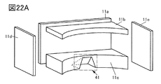
- the housing 11 can have a configuration in which a plurality of housings are connected. Examples of the configuration of the housing 11 are shown in FIGS. 22A, 22B, 22C, 23A and 23B.
- FIG. 22A shows an example in which the housing 11 has the first part 11a to the fifth part 11e.
- 22A shows a configuration in which the first portion 12a to the fifth portion 12e shown in FIGS. 4A to 4C correspond to the first part 11a to the fifth part 11e, respectively.
- the first part 11a to the fifth part 11e are connected to each other to form the housing 11. Further, any one or more of the first part 11a to the fifth part 11e may be detachable from the housing 11.
- FIG. 22B shows an example in which the housing 11 has a fourth part 11d, a fifth part 11e, and a sixth part 11f.
- FIG. 22B shows a configuration having a sixth part 11f in which the first portion 12a to the third portion 12c shown in FIGS. 4A to 4C are integrated.
- the fourth part 11d, the fifth part 11e, and the sixth part 11f are connected to each other to form the housing 11. Further, any one or more of the fourth part 11d, the fifth part 11e, and the sixth part 11f may be detachable from the housing 11.
- FIG. 22C shows an example in which the housing 11 has the first part 11a and the seventh part 11g.
- FIG. 22C shows a configuration having a seventh part 11g in which the second portion 12b to the fifth portion 12e shown in FIGS. 4A to 4C are integrated.
- the first part 11a and the seventh part 11g are connected to each other to form the housing 11. Further, any one of the first part 11a and the seventh part 11g may be detachable from the housing 11.
- FIG. 23A shows an example in which the housing 11 has a second part 11b, a third part 11c, and an eighth part 11h.
- FIG. 23A shows a configuration having an eighth part 11h in which the first portion 12a, the fourth portion 12d, and the fifth portion 12e shown in FIGS. 4A to 4C are integrated.
- the second part 11b, the third part 11c, and the eighth part 11h are connected to each other to form the housing 11. Further, any one or more of the second part 11b, the third part 11c and the eighth part 11h may be detachable from the housing 11.
- FIG. 23B shows an example in which the housing 11 has a third part 11c and a ninth part 11i.
- FIG. 23B shows a configuration having a seventh part 11g in which the first portion 12a, the second portion 12b, the fourth portion 12d, and the fifth portion 12e shown in FIGS. 4A to 4C are integrated. There is.
- the third part 11c and the ninth part 11i are connected to each other to form the housing 11. Further, any of the third part 11c and the ninth part 11i may be detachable from the housing 11.
- FIGS. 22A to 22C, 23A and 23B each part is shown separately for the sake of clarity of the figure.
- the housing 11 By connecting a plurality of parts to form the housing 11, it is possible to easily load the parts (arithmetic unit 19 and the like) provided in the electronic device 10.
- the parts are loaded into each of the first part 11a to the fifth part 11e, and then the first part 11a to the first part 11a to the first part 11a to the fifth part 11e.
- the 5 parts 11e can be connected, and the productivity can be improved as compared with the case where the first part 11a to the fifth part 11e are connected and then the parts are loaded.
- the parts can be easily replaced in the event of a failure.
- the shape of the housing 11 is not particularly limited to the shape shown in FIG. 2A and the like. Each portion constituting the housing 11 may have a curved surface. An example of the housing 11 having a curved surface is shown in FIG. 24A.
- the housing 11 has a curved surface, the design of the electronic device, which is one aspect of the present invention, can be enhanced. Further, since the housing 11 has a curved surface and the number of corners is reduced, injury can be prevented even if the user comes into contact with the housing 11, and the safety of the electronic device, which is one aspect of the present invention, can be enhanced. ..
- the electronic device may have a fixture 25 as shown in FIG. 24B.
- the housing 11 can be fixed to the user's head.
- the fixture 25 is shown in a band shape in FIG. 24B, one aspect of the present invention is not limited to this.
- FIG. 24B shows a configuration in which one end of the fixture 25 is fixed to the housing 11 by the fastener 27, another configuration may be used. For example, it may be configured without the fastener 27.
- This embodiment can be implemented by appropriately combining at least a part thereof with other embodiments described in the present specification.
- FIG. 25 shows a block diagram showing a configuration example of a display device that can be applied to the electronic device of one aspect of the present invention.
- the display device 810 shown in FIG. 25 has a layer 820 and a layer 830 laminated above the layer 820.
- the layer 820 has a gate driver circuit 821, a source driver circuit 822, and a circuit 840.
- the layer 830 has pixels 834, and the pixels 834 are arranged in a matrix to form a pixel array 833.
- An interlayer insulator can be provided between the layer 820 and the layer 830.
- the layer 820 may be laminated above the layer 830.
- the circuit 840 is electrically connected to the source driver circuit 822.
- the circuit 840 may be electrically connected to other circuits or the like.
- Pixels 834 in the same row are electrically connected to the gate driver circuit 821 via wiring 831, and pixels 834 in the same column are electrically connected to the source driver circuit 822 via wiring 832.
- the wiring 831 has a function as a scanning line, and the wiring 832 has a function as a data line.
- FIG. 25 shows a configuration in which one row of pixels 834 is electrically connected by one wiring 831 and one row of pixels 834 is electrically connected by one wiring 832.
- one row of pixels 834 may be electrically connected by two or more wires 831 or one row of pixels 834 may be electrically connected by two or more wires 832. That is, for example, one pixel 834 may be electrically connected to two or more scanning lines, or may be electrically connected to two or more data lines.
- one wiring 831 may be electrically connected to two or more rows of pixels 834, or one wiring 832 may be electrically connected to two or more columns of pixels 834. .. That is, for example, one wiring 831 may be shared by pixels 834 having two or more rows, or one wiring 832 may be shared by pixels 834 having two or more columns.
- the gate driver circuit 821 has a function of generating a signal for controlling the operation of the pixel 834 and supplying the signal to the pixel 834 via the wiring 831.
- the source driver circuit 822 has a function of generating an image signal and supplying the signal to the pixel 834 via the wiring 832.
- the circuit 840 has, for example, a function of receiving image data that is the basis of an image signal generated by the source driver circuit 822 and supplying the received image data to the source driver circuit 822. Further, the circuit 840 has a function as a control circuit that generates a start pulse signal, a clock signal, and the like. In addition, the circuit 840 may be a circuit having a function that the gate driver circuit 821 and the source driver circuit 822 do not have.
- the pixel array 833 has a function of displaying an image corresponding to the image signal supplied to the pixel 834 by the source driver circuit 822. Specifically, an image is displayed on the pixel array 833 by emitting light having a brightness corresponding to the image signal from the pixel 834.
- the positional relationship between the layer 820 and the layer 830 is shown by a alternate long and short dash line and a white circle, and the white circles of the layer 820 and the white circles of the layer 830 overlap each other. ing. The same notation is used in other figures.
- the display device 810 has an area in which the gate driver circuit 821 and the source driver circuit 822 provided in the layer 820 overlap with the pixel array 833.
- the gate driver circuit 821 and the source driver circuit 822 have an area that overlaps with the pixel 834.
- the display device 810 can be made narrower and smaller by stacking the gate driver circuit 821, the source driver circuit 822, and the pixel array 833 so as to have regions that overlap each other. it can.
- the gate driver circuit 821 and the source driver circuit 822 are not clearly separated and have overlapping regions.
- the area is referred to as area 823.
- the region 823 By having the region 823, the occupied area of the gate driver circuit 821 and the source driver circuit 822 can be reduced. Therefore, even when the area of the pixel array 833 is small, the gate driver circuit 821 and the source driver circuit 822 can be provided without protruding from the pixel array 833.
- the area of the region of the gate driver circuit 821 and the source driver circuit 822 that does not overlap with the pixel array 833 can be reduced. From the above, the frame can be further narrowed and the size can be reduced as compared with the case where the area 823 is not provided.
- the circuit 840 can be provided so as not to overlap the pixel array 833.
- the circuit 840 may be provided so as to have a region overlapping the pixel array 833.
- FIG. 25 shows a configuration example in which one gate driver circuit 821 and one source driver circuit 822 are provided on the layer 820 and one pixel array 833 is provided on the layer 830.
- the pixel array 833 is provided on the layer 830. May be provided in plurality. That is, the pixel array provided on the layer 830 may be divided.
- FIG. 25 shows a configuration example in which the circuit 840 is provided on the layer 820, but the circuit 840 may not be provided on the layer 820.
- FIG. 26 is a modification of the configuration shown in FIG. 25, and shows a configuration example of the display device 810 when the circuit 840 is provided on the layer 830.
- the elements constituting the circuit 840 may be dispersedly provided in the layers 820 and 830.
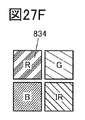
- FIG. 27A to 27E are diagrams for explaining the colors exhibited by the pixels 834 provided in the display device 810.
- a pixel 834 having a function of emitting blue light (B) are provided.
- a pixel 834 having a function of emitting cyan (C) light a pixel 834 having a function of emitting magenta (M) light, and a function of emitting yellow (Y) light.
- the pixel 834 having the above may be provided in the display device 810.
- Pixels 834 having a function of emitting white light (W) may be provided in the display device 810.
- pixel 834 having a function of emitting yellow (Y) light may be provided in the display device 810.
- a pixel 834 having a function of emitting cyan (C) light, a pixel 834 having a function of emitting magenta (M) light, and a function of emitting yellow (Y) light are provided.
- the display device 810 may be provided with a pixel 834 having a pixel 834 and a pixel 834 having a function of emitting white light (W).
- the brightness of the displayed image can be increased by providing the display device 810 with pixels 834 having a function of emitting white light (W). Further, as shown in FIG. 27D and the like, by increasing the types of colors emitted by the pixel 834, the reproducibility of intermediate colors can be improved, so that the display quality can be improved.
- the display device 810 emits pixel 834 having a function of emitting red light (R), pixel 834 having a function of emitting green light (G), and blue light (B).
- the pixel 834 having the function of emitting infrared light (IR) may be provided.
- the display device 810 has a pixel 834 having a function of emitting cyan (C) light, a pixel 834 having a function of emitting magenta (M) light, and a yellow (Y) light.
- the pixel 834 having the function of emitting infrared light (IR) may be provided.
- the display device 810 may have pixels 834 having a function of emitting white light (W) in addition to the pixels 834 shown in FIGS. 27F and 27G.
- the 28A and 28B are circuit diagrams showing a configuration example of the pixel 834.
- the pixel 834 having the configuration shown in FIG. 28A includes a transistor 552, a transistor 554, a capacitance element 562, and a light emitting device 572.
- As the light emitting device 572 for example, an EL device utilizing electroluminescence can be applied.
- the EL device has a layer containing a luminescent compound (hereinafter, also referred to as an EL layer) between a pair of electrodes. When a potential difference larger than the threshold voltage of the EL device is generated between the pair of electrodes, holes are injected into the EL layer from the anode side and electrons are injected from the cathode side. The injected electrons and holes are recombined in the EL layer, and the luminescent substance contained in the EL layer emits light.
- a luminescent compound hereinafter, also referred to as an EL layer
- EL devices are distinguished by whether the light emitting material is an organic compound or an inorganic compound, and the former is generally called an organic EL device and the latter is called an inorganic EL device.
- an organic EL device In an organic EL device, electrons are injected from one electrode and holes are injected into the EL layer from the other electrode by applying a voltage. Then, when those carriers (electrons and holes) are recombined, the luminescent organic compound forms an excited state, and when the excited state returns to the ground state, it emits light. Due to such a mechanism, such a light emitting device is called a current excitation type light emitting device.
- the EL layer is a substance having a high hole injection property, a substance having a high hole transport property, a hole blocking material, a substance having a high electron transport property, a substance having a high electron transfer property, or a bipolar. It may have a sex substance (a substance having high electron transport property and hole transport property) and the like.
- the EL layer can be formed by a vapor deposition method (including a vacuum vapor deposition method), a transfer method, a printing method, an inkjet method, a coating method, or the like.
- Inorganic EL devices are classified into dispersed inorganic EL devices and thin film type inorganic EL devices according to their device configurations.
- the dispersed inorganic EL device has a light emitting layer in which particles of a light emitting material are dispersed in a binder, and the light emitting mechanism is donor-acceptor recombination type light emission utilizing a donor level and an acceptor level.
- the thin-film inorganic EL device has a structure in which a light emitting layer is sandwiched between dielectric layers and further sandwiched between electrodes, and the light emitting mechanism is localized light emission utilizing the inner-shell electron transition of metal ions.
- the light emitting device may have at least one of a pair of electrodes transparent in order to extract light emission. Then, a transistor and a light emitting device are formed on the substrate, and a top emission (top emission) structure that extracts light emission from the surface opposite to the substrate, a bottom emission (bottom emission) structure that extracts light emission from the surface on the substrate side, and There is a double-sided emission (dual emission) light emitting device that extracts light from both sides, and any light emitting device with an injection structure can be applied.
- the same device as the light emitting device 572 can be used.
- One of the source and drain of the transistor 552 is electrically connected to the wiring 832.
- the other of the source or drain of transistor 552 is electrically connected to one electrode of the capacitive element 562 and the gate of transistor 554.
- the other electrode of the capacitive element 562 is electrically connected to the wiring 835a.
- the gate of transistor 552 is electrically connected to wiring 831.
- One of the source and drain of the transistor 554 is electrically connected to the wiring 835a.
- the other of the source or drain of the transistor 554 is electrically connected to one electrode of the light emitting device 572.
- the other electrode of the light emitting device 572 is electrically connected to the wiring 835b.
- the potential VSS is supplied to the wiring 835a
- the potential VDD is supplied to the wiring 835b.
- the wiring 835a and the wiring 835b have a function as a power supply line.
- the emission brightness from the light emitting device 572 is controlled by controlling the current flowing through the light emitting device 572 according to the potential supplied to the gate of the transistor 554.
- FIG. 28B shows a configuration different from the pixel 834 having the configuration shown in FIG. 28A.
- one of the source and the drain of the transistor 552 is electrically connected to the wiring 832.
- the other of the source or drain of transistor 552 is electrically connected to one electrode of the capacitive element 562 and the gate of transistor 554.
- the gate of transistor 552 is electrically connected to wiring 831.
- One of the source and drain of the transistor 554 is electrically connected to the wiring 835a.
- the other of the source or drain of the transistor 554 is electrically connected to the other electrode of the capacitive element 562 and one electrode of the light emitting device 572.
- the other electrode of the light emitting device 572 is electrically connected to the wiring 835b.
- the potential VDD is supplied to the wiring 835a
- the potential VSS is supplied to the wiring 835b.
- FIG. 29A is a configuration example of the pixel 834, which is different from the pixel 834 having the configuration shown in FIGS. 28A and 28B in that it has a memory.
- the pixel 834 having the configuration shown in FIG. 29A includes a transistor 511, a transistor 513, a transistor 521, a capacitive element 515, a capacitive element 517, and a light emitting device 572. Further, wiring 831_1 and wiring 831_2 are electrically connected to the pixel 834 as wiring 831 having a function as a scanning line, and wiring 832_1 and wiring 832_2 are electrically connected to the pixel 834 as wiring 832 having a function as a data line. There is.
- One of the source and drain of the transistor 511 is electrically connected to the wiring 832_1.
- the other of the source or drain of the transistor 511 is electrically connected to one electrode of the capacitive element 515.
- the gate of transistor 511 is electrically connected to wiring 831_1.
- One of the source and drain of the transistor 513 is electrically connected to the wiring 832_2.
- the other of the source or drain of the transistor 513 is electrically connected to the other electrode of the capacitive element 515.
- the gate of transistor 513 is electrically connected to wiring 831_2.
- the other electrode of the capacitive element 515 is electrically connected to one electrode of the capacitive element 517.
- One electrode of the capacitive element 517 is electrically connected to the gate of the transistor 521.
- One of the source or drain of the transistor 521 is electrically connected to one electrode of the light emitting device 572.
- the other electrode of the capacitive element 517 is electrically connected to the wiring 535.
- the other side of the source or drain of transistor 521 is electrically connected to wire 537.
- the other electrode of the light emitting device 572 is electrically connected to the wiring 539.
- the voltage supplied to the light emitting device indicates the difference between the potential applied to one electrode of the light emitting device and the potential applied to the other electrode of the light emitting device.
- Node N1 is a node in which the other electrode of the source or drain of the transistor 511 and one electrode of the capacitive element 515 are electrically connected.
- a node in which the other of the source or drain of the transistor 513, one electrode of the capacitive element 517, and the gate of the transistor 521 are electrically connected is referred to as a node N2.
- the circuit composed of the capacitance element 517, the transistor 521, and the light emitting device 572 is referred to as a circuit 401.
- the wiring 535 can be a common wiring for, for example, all the pixels 834 provided in the display device 810.
- the potential supplied to the wiring 535 is a common potential.
- a constant potential can be supplied to the wiring 537 and the wiring 539.
- the wiring 537 can be supplied with a high potential, and the wiring 539 can be supplied with a low potential.
- the wiring 537 and the wiring 539 have a function as a power supply line.
- the transistor 521 has a function of controlling the current supplied to the light emitting device 572.
- the capacitance element 517 has a function as a holding capacitance.
- the capacitive element 517 may be omitted.
- FIG. 29A shows a configuration in which the anode side of the light emitting device 572 is electrically connected to the transistor 521
- the transistor 521 may be electrically connected to the cathode side.
- the potential value of the wiring 537 and the potential value of the wiring 539 can be changed as appropriate.
- the pixel 834 can hold the potential of the node N1 by turning off the transistor 511. Further, by turning off the transistor 513, the potential of the node N2 can be maintained. Further, by turning off the transistor 513 and writing a predetermined potential to the node N1 via the transistor 511, the potential of the node N2 is changed according to the displacement of the potential of the node N1 by the capacitive coupling via the capacitive element 515. Can be made to.
- a transistor having a metal oxide in the channel forming region (hereinafter, also referred to as an OS transistor) can be applied to the transistor 511 and the transistor 513.
- the bandgap of the metal oxide can be 2 eV or more, or 2.5 eV or more. Therefore, the leakage current (off current) of the OS transistor becomes extremely small in the non-conducting state. Therefore, by applying the OS transistor to the transistor 511 and the transistor 513, the potentials of the node N1 and the node N2 can be maintained for a long period of time.
- In-M-Zn oxide (element M is aluminum, gallium, yttrium, tin, copper, vanadium, beryllium, boron, titanium, iron, nickel, germanium, zirconium, molybdenum, lantern, cerium, neodymium) , Hafnium, tantalum, tungsten, gallium, etc. (one or more) and the like may be used.
- element M aluminum, gallium, yttrium, or tin may be used.
- the metal oxide indium oxide, zinc oxide, In-Ga oxide, In-Zn oxide, Ga-Zn oxide, or gallium oxide may be used.
- FIG. 29B is a timing chart relating to the operation of the pixel 834 having the configuration shown in FIG. 29A.
- the effects of various resistors such as wiring resistance, parasitic capacitance of transistors and wiring, and the threshold voltage of transistors are not considered here.
- one frame period is divided into a period T1 and a period T2.
- the period T1 is a period for writing the potential to the node N2
- the period T2 is a period for writing the potential to the node N1.
- both the wiring 831_1 and the wiring 831_2 are supplied with a potential for turning on the transistor. Further, the potential V ref , which is a fixed potential, is supplied to the wiring 832_1, and the potential V w is supplied to the wiring 832_1.
- the potential V ref is supplied to the node N1 from the wiring 832_1 via the transistor 511. Further, the potential V w is supplied to the node N2 from the wiring 832_2 via the transistor 513. Therefore, the capacitance element 515 is in a state where the potential difference V w ⁇ V ref is held.
- the electric potential for turning on the transistor 511 is supplied to the wiring 831_1, and the potential for turning off the transistor 513 is supplied to the wiring 831_2. Further, the electric potential V data is supplied to the wiring 832_1, and a predetermined constant potential is supplied to the wiring 832_1.
- the potential of the wiring 832_2 may be floating.
- the potential V data is supplied to the node N1 via the transistor 511.
- the potential of the node N2 changes by the potential dV according to the potential V data due to the capacitive coupling by the capacitive element 515. That is, the potential obtained by adding the potential V w and the potential dV is input to the circuit 401.
- dV is shown to be a positive value in FIG. 29B, it may be a negative value. That is, the potential V data may be lower than the potential V ref.
- the potential dV is roughly determined by the capacitance value of the capacitance element 515 and the capacitance value of the circuit 401.
- the potential dV becomes a potential close to the potential difference V data ⁇ V ref.
- the image displayed on the pixel array 833 can be corrected inside the pixel 834.
- one of the two types of data signals can be the image signal described above, and the other of the two types of data signals can be, for example, a correction signal.
- the image signal can be corrected by the correction signal. Not only the image signal but also the correction signal and the like can be generated by the source driver circuit 822 of the display device 810.
- the pixel 834 having the configuration shown in FIG. 29A can have the potential of the node N2 exceeding the maximum potential that can be supplied to the wiring 832_1 and the wiring 832_2.
- a high voltage can be supplied to the light emitting device 572.
- the potential of the wiring 537 can be increased. Therefore, when the light emitting device 572 is an organic EL device, the light emitting device can have a tandem structure described later. Thereby, the current efficiency and the external quantum efficiency of the light emitting device 572 can be increased. Therefore, a high-luminance image can be displayed on the display device 810. In addition, the power consumption of the display device 810 can be reduced.
- the circuit is not limited to the circuit illustrated in FIG. 29A, and a transistor, a capacitive element, or the like may be added separately.
- the number of nodes capable of holding the potential can be increased to three. That is, another node capable of holding the potential can be provided in the pixel 834 in addition to the node N1 and the node N2.
- the potential of the node N2 can be further increased. Therefore, a larger current can be passed through the light emitting device 572.
- FIGS. 30A to 30E are diagrams showing a configuration example of a circuit 401 different from that of FIG. 30A.
- the circuit 401 having the configuration shown in FIG. 30A has a capacitance element 517, a transistor 521, and a light emitting device 572, similarly to the circuit 401 having the configuration shown in FIG. 29A.
- the gate of the transistor 521 and one electrode of the capacitive element 517 are electrically connected to the node N2.
- One of the source and drain of the transistor 521 is electrically connected to the wiring 537.
- the other of the source or drain of the transistor 521 is electrically connected to the other electrode of the capacitive element 517.
- the other electrode of the capacitive element 517 is electrically connected to one electrode of the light emitting device 572.
- the other electrode of the light emitting device 572 is electrically connected to the wiring 539.
- the circuit 401 having the configuration shown in FIG. 30B also has a capacitance element 517, a transistor 521, and a light emitting device 572, similarly to the circuit 401 having the configuration shown in FIG. 29A.
- the gate of the transistor 521 and one electrode of the capacitive element 517 are electrically connected to the node N2.
- One electrode of the light emitting device 572 is electrically connected to the wiring 537.
- the other electrode of the light emitting device 572 is electrically connected to one of the source or drain of the transistor 521.
- the other of the source or drain of the transistor 521 is electrically connected to the other electrode of the capacitive element 517.
- the other electrode of the capacitive element 517 is electrically connected to the wiring 539.
- FIG. 30C shows a configuration example of the circuit 401 when the transistor 525 is added to the circuit 401 shown in FIG. 30A.
- One of the source or drain of the transistor 525 is electrically connected to the other of the source or drain of the transistor 521 and the other electrode of the capacitive element 517.
- the other of the source or drain of the transistor 525 is electrically connected to one electrode of the light emitting device 572.
- the gate of transistor 525 is electrically connected to wiring 541.
- the wiring 541 has a function as a scanning line for controlling the continuity of the transistor 525.
- FIG. 30D shows a configuration example of the circuit 401 when the transistor 527 is added to the circuit 401 shown in FIG. 30C.
- One of the source or drain of transistor 527 is electrically connected to the other of the source or drain of transistor 521.
- the other of the source or drain of transistor 527 is electrically connected to wire 543.
- the gate of transistor 527 is electrically connected to wiring 545.
- the wiring 545 has a function as a scanning line for controlling the continuity of the transistor 527.
- the wiring 543 can be electrically connected to a supply source of a specific potential such as a reference potential. That is, the wiring 543 has a function as a power supply line. By supplying a specific potential from the wiring 543 to the other of the source or drain of the transistor 521, it is possible to stabilize the writing of the image signal to the pixel 834.
- Wiring 543 can be electrically connected to circuit 520.
- the circuit 520 can have one or more of the above-mentioned specific potential supply source, a function of acquiring the electrical characteristics of the transistor 521, and a function of generating a correction signal.
- the circuit 401 having the configuration shown in FIG. 30E includes a capacitance element 517, a transistor 521, a transistor 529, and a light emitting device 572.
- the gate of the transistor 521 and one electrode of the capacitive element 517 are electrically connected to the node N2.
- One of the source and drain of the transistor 521 is electrically connected to the wiring 537.
- One of the source or drain of the transistor 529 is electrically connected to the wiring 543.
- the other electrode of the capacitive element 517 is electrically connected to the other of the source or drain of the transistor 521.
- the other of the source or drain of transistor 521 is electrically connected to the other of the source or drain of transistor 529.
- the other of the source or drain of the transistor 529 is electrically connected to one electrode of the light emitting device 572.
- the gate of the transistor 529 is electrically connected to the wiring 831_1.
- the other electrode of the light emitting device 572 is electrically connected to the wiring 539.
- FIG. 31 is a block diagram showing a configuration example of the display device 810 when the pixel 834 has the configuration shown in FIG. 29A.
- the display device 810 having the configuration shown in FIG. 31 is provided with a demultiplexer circuit 824 in addition to the components of the display device 810 shown in FIG. 25.
- the demultiplexer circuit 824 can be provided, for example, in layer 820, as shown in FIG.
- the number of demultiplexer circuits 824 can be, for example, the same as the number of columns of pixels 834 provided in the pixel array 833.
- the gate driver circuit 821 is electrically connected to the pixel 834 via the wiring 831-1.
- the gate driver circuit 821 is electrically connected to the pixel 834 via wiring 831-2.
- the wiring 831-1 and the wiring 831-2 have a function as scanning lines.
- the source driver circuit 822 is electrically connected to the input terminal of the demultiplexer circuit 824.
- the first output terminal of the demultiplexer circuit 824 is electrically connected to the pixel 834 via the wiring 832-1.
- the second output terminal of the demultiplexer circuit 824 is electrically connected to the pixel 834 via the wiring 832-2.
- the wiring 832-1 and the wiring 832-2 have a function as a data line.
- the source driver circuit 822 and the demultiplexer circuit 824 may be collectively referred to as a source driver circuit. That is, the demultiplexer circuit 824 may be included in the source driver circuit 822.
- the source driver circuit 822 has a function of generating the image signal S1 and the image signal S2.
- the demultiplexer circuit 824 has a function of supplying the image signal S1 to the pixel 834 via the wiring 832-1 and a function of supplying the image signal S2 to the pixel 834 via the wiring 832-2.
- the potential V data can be set to the potential corresponding to the image signal S1
- the potential V w corresponds to the image signal S2. Can be the potential to be.
- the potential of the node N2 becomes “V w + dV”.
- the potential dV is the potential corresponding to the potential V data. Therefore, the image signal S1 can be added to the image signal S2. That is, the image signal S1 can be superimposed on the image signal S2.
- the magnitudes of the potential V data corresponding to the image signal S1 and the potential V w corresponding to the image signal S2 are limited according to the withstand voltage of the source driver circuit 822 and the like. Therefore, by superimposing the image signal S1 and the image signal S2, an image corresponding to the image signal having a potential higher than the potential that can be output by the source driver circuit 822 can be displayed on the pixel array 833. As a result, a large current can be passed through the light emitting device 572, so that a high-luminance image can be displayed on the pixel array 833.
- the dynamic range which is the range of brightness of the image that can be displayed by the pixel array 833, can be expanded.
- the image corresponding to the image signal S1 and the image corresponding to the image signal S2 may be the same or different.
- the pixel array 833 has the brightness of the image corresponding to the image signal S1 and the brightness of the image corresponding to the image signal S2. An image with higher brightness can be displayed.
- FIG. 32 shows a case where the image P1 corresponding to the image signal S1 contains only characters and the image P2 corresponding to the image signal S2 contains a picture and characters.
- the brightness of the characters can be increased, and for example, the characters can be emphasized.
- FIG. 29B after the potential V w is written to the node N2, the potential of the node N2 changes according to the potential V data. Therefore, when rewriting the potential V w corresponding to the image signal S2, , The potential V data of the image signal S1 must be written again.
- the image P2 is an image that is rewritten less frequently than the image P1.
- FIG. 32 shows an example in which the image P1 contains only characters and the image P2 contains pictures and characters, one aspect of the present invention is not limited to this.
- FIG. 33 is a cross-sectional view showing a configuration example of the display device 810.
- the display device 810 has a substrate 701 and a substrate 705, and the substrate 701 and the substrate 705 are bonded to each other by a sealing material 712.
- a single crystal semiconductor substrate such as a single crystal silicon substrate can be used.
- a semiconductor substrate other than the single crystal semiconductor substrate may be used as the substrate 701.
- a transistor 441 and a transistor 601 are provided on the substrate 701.
- the transistor 441 can be a transistor provided in the circuit 840.
- the transistor 601 can be a transistor provided in the gate driver circuit 821 or a transistor provided in the source driver circuit 822. That is, the transistor 441 and the transistor 601 can be provided on the layer 820 shown in FIG. 25 and the like.
- the transistor 441 is composed of a conductor 443 having a function as a gate electrode, an insulator 445 having a function as a gate insulator, and a part of a substrate 701, and is a semiconductor region 447 including a channel forming region and a source region. Alternatively, it has a low resistance region 449a that functions as one of the drain regions and a low resistance region 449b that functions as the other of the source region or the drain region.
- the transistor 441 may be either a p-channel type or an n-channel type.
- the transistor 441 is electrically separated from other transistors by the element separation layer 403.
- FIG. 33 shows a case where the transistor 441 and the transistor 601 are electrically separated by the element separation layer 403.
- the element separation layer 403 can be formed by using a LOCOS (LOCOxidation of Silicon) method, an STI (Shallow Trench Isolation) method, or the like.
- the semiconductor region 447 has a convex shape. Further, the side surface and the upper surface of the semiconductor region 447 are provided so as to be covered with the conductor 443 via the insulator 445. Note that FIG. 33 does not show how the conductor 443 covers the side surface of the semiconductor region 447. Further, a material for adjusting the work function can be used for the conductor 443.
- a transistor having a convex shape in the semiconductor region such as the transistor 441 can be called a fin type transistor because the convex portion of the semiconductor substrate is used.
- an insulator which is in contact with the upper part of the convex portion and has a function as a mask for forming the convex portion may be provided.
- FIG. 33 shows a configuration in which a part of the substrate 701 is processed to form a convex portion, the SOI substrate may be processed to form a semiconductor having a convex shape.
- the configuration of the transistor 441 shown in FIG. 33 is an example, and is not limited to the configuration, and may be an appropriate configuration according to the circuit configuration, the operation method of the circuit, and the like.
- the transistor 441 may be a planar transistor.
- the transistor 601 can have the same configuration as the transistor 441.
- an insulator 405, an insulator 407, an insulator 409, and an insulator 411 are provided.
- the conductor 451 is embedded in the insulator 405, the insulator 407, the insulator 409, and the insulator 411.
- the height of the upper surface of the conductor 451 and the height of the upper surface of the insulator 411 can be made about the same.
- Insulator 413 and insulator 415 are provided on the conductor 451 and the insulator 411. Further, the conductor 457 is embedded in the insulator 413 and the insulator 415.
- Insulator 417 and insulator 419 are provided on the conductor 457 and the insulator 415. Further, the conductor 459 is embedded in the insulator 417 and the insulator 419.
- Insulator 421 and insulator 214 are provided on the conductor 459 and the insulator 419.
- the conductor 453 is embedded in the insulator 421 and in the insulator 214.
- the height of the upper surface of the conductor 453 and the height of the upper surface of the insulator 214 can be made about the same.
- Insulator 216 is provided on the conductor 453 and on the insulator 214.
- a conductor 455 is embedded in the insulator 216.
- the height of the upper surface of the conductor 455 and the height of the upper surface of the insulator 216 can be made about the same.
- Insulator 222, insulator 224, insulator 254, insulator 244, insulator 280, insulator 274, and insulator 281 are provided on the conductor 455 and the insulator 216.
- the conductor 305 is embedded in the insulator 222, the insulator 224, the insulator 254, the insulator 244, the insulator 280, the insulator 274, and the insulator 281.
- the height of the upper surface of the conductor 305 and the height of the upper surface of the insulator 281 can be made about the same.
- the insulator 361 is provided on the conductor 305 and the insulator 281.
- a conductor 317 and a conductor 337 are embedded in the insulator 361.
- the height of the upper surface of the conductor 337 and the height of the upper surface of the insulator 361 can be made about the same.
- the insulator 363 is provided on the conductor 337 and the insulator 361.
- a conductor 347, a conductor 353, a conductor 355, and a conductor 357 are embedded in the insulator 363.
- the height of the upper surface of the conductor 353, the conductor 355, and the conductor 357 can be made the same as the height of the upper surface of the insulator 363.
- connection electrode 760 is provided on the conductor 353, the conductor 355, the conductor 357, and the insulator 363. Further, an anisotropic conductor 780 is provided so as to be electrically connected to the connection electrode 760, and an FPC (Flexible Printed Circuit) 716 is provided so as to be electrically connected to the anisotropic conductor 780.
- FPC Flexible Printed Circuit
- the low resistance region 449b having a function as the other of the source region and the drain region of the transistor 441 includes a conductor 451 and a conductor 457, a conductor 459, a conductor 453, a conductor 455, and a conductor. It is electrically connected to the FPC 716 via 305, conductor 317, conductor 337, conductor 347, conductor 353, conductor 355, conductor 357, connection electrode 760, and anisotropic conductor 780. ..
- connection electrode 760 and the conductor 347 shows three conductors having a function of electrically connecting the connection electrode 760 and the conductor 347, that is, the conductor 353, the conductor 355, and the conductor 357, which is one of the present inventions.
- the aspect is not limited to this.
- the number of conductors having a function of electrically connecting the connection electrode 760 and the conductor 347 may be one, two, or four or more.
- the contact resistance can be reduced by providing a plurality of conductors having a function of electrically connecting the connection electrode 760 and the conductor 347.
- a transistor 750 is provided on the insulator 214.
- the transistor 750 can be a transistor provided in the pixel 834. That is, the transistor 750 can be provided on the layer 830 shown in FIG. 25 and the like.
- an OS transistor can be used as the transistor 750.
- the OS transistor has a feature that the off-current is extremely low. Therefore, since the holding time of the image signal or the like can be lengthened, the frequency of the refresh operation can be reduced. Therefore, the power consumption of the display device 810 can be reduced.
- Conductors 301a and 301b are embedded in the insulator 254, the insulator 244, the insulator 280, the insulator 274, and the insulator 281.
- the conductor 301a is electrically connected to one of the source or drain of the transistor 750
- the conductor 301b is electrically connected to the other of the source or drain of the transistor 750.
- the height of the upper surfaces of the conductors 301a and 301b and the height of the upper surfaces of the insulator 281 can be made about the same.
- a conductor 311, a conductor 313, a conductor 331, a capacitance element 790, a conductor 333, and a conductor 335 are embedded in the insulator 361.
- the conductors 311 and 313 are electrically connected to the transistor 750 and have a function as wiring.
- the conductor 333 and the conductor 335 are electrically connected to the capacitive element 790.
- the height of the upper surface of the conductor 331, the conductor 333, and the conductor 335 can be made the same as the height of the upper surface of the insulator 361.
- Conductor 341, conductor 343, and conductor 351 are embedded in the insulator 363.
- the height of the upper surface of the conductor 351 and the height of the upper surface of the insulator 363 can be made about the same.
- the 281, the insulator 361, and the insulator 363 have a function as an interlayer film, and may have a function as a flattening film that covers the uneven shape below each of them.
- the upper surface of the insulator 363 may be flattened by a flattening treatment using a chemical mechanical polishing (CMP) method or the like in order to improve the flatness.
- CMP chemical mechanical polishing
- the capacitive element 790 has a lower electrode 321 and an upper electrode 325. Further, an insulator 323 is provided between the lower electrode 321 and the upper electrode 325. That is, the capacitive element 790 has a laminated structure in which an insulator 323 that functions as a dielectric is sandwiched between a pair of electrodes.
- FIG. 33 shows an example in which the capacitance element 790 is provided on the insulator 281, the capacitance element 790 may be provided on an insulator different from the insulator 281.
- FIG. 33 shows an example in which the conductor 301a, the conductor 301b, and the conductor 305 are formed in the same layer. Further, an example is shown in which the conductor 311 and the conductor 313, the conductor 317, and the lower electrode 321 are formed in the same layer. Further, an example is shown in which the conductor 331, the conductor 333, the conductor 335, and the conductor 337 are formed in the same layer. Further, an example is shown in which the conductor 341, the conductor 343, and the conductor 347 are formed in the same layer. Further, an example is shown in which the conductor 351 and the conductor 353, the conductor 355, and the conductor 357 are formed in the same layer.
- the display device 810 shown in FIG. 33 has a light emitting device 572.
- the light emitting device 572 has a conductor 772, an EL layer 786, and a conductor 788.
- the conductor 788 is provided on the substrate 705 side and has a function as a common electrode. Further, the conductor 772 is electrically connected to the other of the source or drain of the transistor 750 via the conductor 351 and the conductor 341, the conductor 331, the conductor 313, and the conductor 301b.
- the conductor 772 is formed on the insulator 363 and has a function as a pixel electrode. Further, the EL layer 786 has an organic compound or an inorganic compound such as a quantum dot.
- Examples of materials that can be used for organic compounds include fluorescent materials and phosphorescent materials.
- Examples of materials that can be used for quantum dots include colloidal quantum dot materials, alloy-type quantum dot materials, core-shell type quantum dot materials, and core-type quantum dot materials.
- an insulator 730 is provided on the insulator 363.
- the insulator 730 can be configured to cover a part of the conductor 772.
- the light emitting device 572 has a translucent conductor 788, and can be a top emission type light emitting device.
- the light emitting device 572 may have a bottom emission structure that emits light to the conductor 772 side, or a dual emission structure that emits light to both the conductor 772 and the conductor 788.
- the light emitting device 572 can have a microcavity structure, which will be described in detail later.
- a predetermined color for example, RGB
- the display device 810 can perform color display.
- the display device 810 can display a high-brightness image, and the power consumption of the display device 810 can be reduced.
- the EL layer 786 is formed in an island shape for each pixel or in a striped shape for each pixel row, that is, when the EL layer 786 is formed by painting separately, it is possible to configure the structure without providing the colored layer.
- the light-shielding layer 738 is provided so as to have a region overlapping with the insulator 730. Further, the light-shielding layer 738 is covered with an insulator 734. Further, the space between the light emitting device 572 and the insulator 734 is filled with a sealing layer 732.
- a structure 778 is provided between the insulator 730 and the EL layer 786. Further, a structure 778 is provided between the insulator 730 and the insulator 734.
- the structure 778 is a columnar spacer and has a function of controlling the distance (cell gap) between the substrate 701 and the substrate 705.
- a spherical spacer may be used as the structure 778.
- a light-shielding layer 738 and an insulator 734 in contact with the light-shielding layer 738 are provided on the substrate 705 side.
- the light-shielding layer 738 has a function of blocking light emitted from an adjacent region.
- the light-shielding layer 738 has a function of blocking external light from reaching the transistor 750 or the like.
- FIG. 34 is a modified example of the display device 810 shown in FIG. 33, and is different from the display device 810 shown in FIG. 33 in that a colored layer 736 is provided.
- the colored layer 736 By providing the colored layer 736, the color purity of the light extracted from the light emitting device 572 can be increased. As a result, a high-quality image can be displayed on the display device 810.
- all the light emitting devices 572 of the display device 810 can be light emitting devices that emit white light, so that the EL layer 786 does not have to be formed by painting separately, and the display device 810 has a high definition. can do.
- FIGS. 33 and 34 the transistor 441 and the transistor 601 are provided so as to form a channel forming region inside the substrate 701, and the OS transistor is provided by laminating the transistor 441 and the transistor 601.
- FIG. 35 is a modification of FIG. 33
- FIG. 36 is a modification of FIG. 34, in which the transistor 750 is provided by being laminated on the OS transistors 602 and 603 instead of the transistor 441 and the transistor 601.
- the display device 810 having the configuration shown in FIGS. 33 and 34 is provided with OS transistors stacked.
- An insulator 613 and an insulator 614 are provided on the substrate 701, and a transistor 602 and a transistor 603 are provided on the insulator 614.
- a transistor or the like may be provided between the substrate 701 and the insulator 613.
- a transistor having the same configuration as the transistor 441 and the transistor 601 shown in FIGS. 33 and 34 may be provided between the substrate 701 and the insulator 613.
- the transistor 602 can be a transistor provided in the circuit 840.
- the transistor 603 can be a transistor provided in the gate driver circuit 821 or a transistor provided in the source driver circuit 822. That is, the transistor 602 and the transistor 603 can be provided on the layer 820 shown in FIG. 25 and the like. As shown in FIG. 26, when the circuit 840 is provided on the layer 830, the transistor 602 can be provided on the layer 830.
- the transistor 602 and the transistor 603 can be a transistor having the same configuration as the transistor 750.
- the transistor 602 and the transistor 603 may be OS transistors having a configuration different from that of the transistor 750.
- an insulator 616, an insulator 622, an insulator 624, an insulator 654, an insulator 644, an insulator 680, an insulator 674, and an insulator 681 are provided on the insulator 614. ..
- the conductor 461 is embedded in the insulator 654, the insulator 644, the insulator 680, the insulator 674, and the insulator 681.
- the height of the upper surface of the conductor 461 and the height of the upper surface of the insulator 681 can be made about the same.
- the insulator 501 is provided on the conductor 461 and the insulator 681.
- a conductor 463 is embedded in the insulator 501.
- the height of the upper surface of the conductor 463 and the height of the upper surface of the insulator 501 can be made about the same.
- the insulator 503 is provided on the conductor 463 and the insulator 501.
- a conductor 465 is embedded in the insulator 503.
- the height of the upper surface of the conductor 465 and the height of the upper surface of the insulator 503 can be made about the same.
- the insulator 505 is provided on the conductor 465 and the insulator 503. Further, the conductor 467 is embedded in the insulator 505.
- the insulator 507 is provided on the conductor 467 and the insulator 505.
- a conductor 469 is embedded in the insulator 507.
- the height of the upper surface of the conductor 469 and the height of the upper surface of the insulator 507 can be made about the same.
- the insulator 509 is provided on the conductor 469 and the insulator 507. Further, the conductor 471 is embedded in the insulator 509.
- Insulator 421 and insulator 214 are provided on the conductor 471 and the insulator 509.
- the conductor 453 is embedded in the insulator 421 and in the insulator 214.
- the height of the upper surface of the conductor 453 and the height of the upper surface of the insulator 214 can be made about the same.
- one of the source or drain of the transistor 602 is a conductor 461, a conductor 463, a conductor 465, a conductor 467, a conductor 469, a conductor 471, a conductor 453, or a conductor. Electrically with FPC716 via 455, conductor 305, conductor 317, conductor 337, conductor 347, conductor 353, conductor 355, conductor 357, connection electrode 760, and anisotropic conductor 780. It is connected.
- the insulator 613, the insulator 614, the insulator 680, the insulator 674, the insulator 681, the insulator 501, the insulator 503, the insulator 505, the insulator 507, and the insulator 509 have a function as an interlayer film. , It may have a function as a flattening film that covers each of the lower uneven shapes.
- the display device 810 By configuring the display device 810 as shown in FIGS. 35 and 36, all the transistors of the display device 810 can be used as OS transistors while the display device 810 is narrowed and downsized. Thereby, for example, the transistor provided in the layer 820 and the transistor provided in the layer 830 can be manufactured by using the same device. Therefore, the manufacturing cost of the display device 810 can be reduced, and the display device 810 can be made inexpensive.
- FIG. 37A to 37E are diagrams showing a configuration example of the light emitting device 572.
- FIG. 37A shows a structure (single structure) in which the EL layer 786 is sandwiched between the conductor 772 and the conductor 788.
- the EL layer 786 contains a light emitting material, for example, a light emitting material which is an organic compound.
- FIG. 37B is a diagram showing a laminated structure of EL layer 786.
- the conductor 772 has a function as an anode
- the conductor 788 has a function as a cathode.
- the EL layer 786 has a structure in which the hole injection layer 721, the hole transport layer 722, the light emitting layer 723, the electron transport layer 724, and the electron injection layer 725 are sequentially laminated on the conductor 772.
- the conductor 772 has a function as a cathode and the conductor 788 has a function as an anode, the stacking order is reversed.
- the light emitting layer 723 has a light emitting material or a plurality of materials in an appropriate combination, and can be configured to obtain fluorescent light emission or phosphorescent light emission exhibiting a desired light emitting color. Further, the light emitting layer 723 may have a laminated structure having different light emitting colors. In this case, different materials may be used for the luminescent substance and other substances used for each of the laminated light emitting layers.
- the conductor 772 shown in FIG. 37B is used as a reflecting electrode
- the conductor 788 is used as a semi-transmissive / semi-reflective electrode
- the EL layer 786 has a micro-optical resonator (microcavity) structure.
- the light emitted from the light emitting layer 723 can be resonated between both electrodes to enhance the light emitted through the conductor 788.
- the conductor 772 of the light emitting device 572 is a reflective electrode having a laminated structure of a conductive material having a reflective property and a conductive material having a translucent property (transparent conductive film)
- the thickness of the transparent conductive film is formed.
- Optical adjustment can be performed by controlling. Specifically, the distance between the electrodes of the conductor 772 and the conductor 788 is adjusted to be close to m ⁇ / 2 (where m is a natural number) with respect to the wavelength ⁇ of the light obtained from the light emitting layer 723. Is preferable.
- the light emitting region referred to here means a recombination region of holes and electrons in the light emitting layer 723.
- the spectrum of a specific monochromatic light obtained from the light emitting layer 723 can be narrowed, and light emission with good color purity can be obtained.
- the optical distance between the conductor 772 and the conductor 788 can be said to be strictly the total thickness from the reflection region of the conductor 772 to the reflection region of the conductor 788.
- the above-mentioned effect can be sufficiently obtained by assuming an arbitrary position of the conductor 772 and the conductor 788 as the reflection region. It shall be possible.
- the optical distance between the conductor 772 and the light emitting layer from which the desired light can be obtained is, strictly speaking, the optical distance between the reflection region of the conductor 772 and the light emitting region in the light emitting layer where the desired light can be obtained. be able to.
- the reflection region and the desired light can be obtained at an arbitrary position of the conductor 772. It is assumed that the above-mentioned effect can be sufficiently obtained by assuming that an arbitrary position of the light emitting layer is a light emitting region.
- the light emitting device 572 shown in FIG. 37B has a microcavity structure, it is possible to extract light of different wavelengths (monochromatic light) even if it has the same EL layer. Therefore, it is not necessary to separately paint (for example, RGB) to obtain different emission colors. Therefore, it is easy to realize high definition. It can also be combined with a colored layer. Further, since it is possible to increase the emission intensity in the front direction of a specific wavelength, it is possible to reduce the power consumption.
- the light emitting device 572 shown in FIG. 37B does not have to have a microcavity structure.
- the light emitting layer 723 has a structure that emits white light, and by providing the colored layer, light of a predetermined color (for example, RGB) can be extracted. Further, when forming the EL layer 786, if different coatings are performed to obtain different emission colors, light of a predetermined color can be taken out without providing a colored layer.
- At least one of the conductor 772 and the conductor 788 can be a translucent electrode (transparent electrode, semi-transmissive / semi-reflective electrode, etc.).
- the electrode having translucency is a transparent electrode
- the transmittance of visible light of the transparent electrode is 40% or more.
- the reflectance of visible light of the semi-transmissive / semi-reflective electrode is 20% or more and 80% or less, preferably 40% or more and 70% or less.
- the resistivity of these electrodes is preferably 1 ⁇ 10 -2 ⁇ cm or less.
- the visible light reflectance of the reflective electrode is 40% or more and 100% or less, preferably 70% or more and 100% or less. And.
- the resistivity of this electrode is preferably 1 ⁇ 10 -2 ⁇ cm or less.
- the configuration of the light emitting device 572 may be the configuration shown in FIG. 37C.
- two EL layers (EL layer 786a and EL layer 786b) are provided between the conductor 772 and the conductor 788, and a charge generation layer 792 is provided between the EL layer 786a and the EL layer 786b.
- the light emitting device 572 having a laminated structure (tandem structure) is shown.
- the current efficiency and the external quantum efficiency of the light emitting device 572 can be improved. Therefore, a high-luminance image can be displayed on the display device 810.
- the power consumption of the display device 810 can be reduced.
- the EL layer 786a and the EL layer 786b can have the same configuration as the EL layer 786 shown in FIG. 37B.
- the charge generation layer 792 injects electrons into one of the EL layer 786a and the EL layer 786b, and injects holes into the other.
- the charge generation layer 792 injects electrons into one of the EL layer 786a and the EL layer 786b, and injects holes into the other.
- a voltage is supplied so that the potential of the conductor 772 is higher than the potential of the conductor 788, electrons are injected from the charge generation layer 792 into the EL layer 786a, and holes are injected from the charge generation layer 792 into the EL layer 786b. Will be done.
- the charge generation layer 792 preferably transmits visible light (specifically, the visible light transmittance of the charge generation layer 792 is 40% or more) from the viewpoint of light extraction efficiency. Further, the conductivity of the charge generation layer 792 may be lower than the conductivity of the conductor 772 or the conductivity of the conductor 788.
- the configuration of the light emitting device 572 may be the configuration shown in FIG. 37D.
- three EL layers (EL layer 786a, EL layer 786b, and EL layer 786c) are provided between the conductor 772 and the conductor 788, and between the EL layer 786a and the EL layer 786b, A tandem-structured light emitting device 572 having a charge generation layer 792 between the EL layer 786b and the EL layer 786c is shown.
- the EL layer 786a, the EL layer 786b, and the EL layer 786c can have the same configuration as the EL layer 786 shown in FIG. 37B.
- the configuration of the light emitting device 572 may be the configuration shown in FIG. 37E.
- n layers of EL layers (EL layers 786 (1) to EL layers 786 (n)) are provided between the conductor 772 and the conductor 788, and electric charges are generated between the respective EL layers 786.
- the tandem structure light emitting device 572 having the layer 792 is shown.
- the EL layer 786 (1) to the EL layer 786 (n) can have the same configuration as the EL layer 786 shown in FIG. 37B.
- FIG. 37E shows the EL layer 786 (1), the EL layer 786 (m), the EL layer 786 (m + 1), and the EL layer 786 (n) among the EL layers 786.
- n is an integer greater than m.
- n is an integer greater than m.
- Conductor 772 and Conductor 788 The following materials can be appropriately combined and used for the conductor 772 and the conductor 788 as long as the functions of the anode and the cathode can be satisfied.
- metals, alloys, electrically conductive compounds, mixtures thereof, and the like can be appropriately used. Specific examples thereof include In—Sn oxide (also referred to as ITO), In—Si—Sn oxide (also referred to as ITSO), In—Zn oxide, and In—W—Zn oxide.
- Other elements belonging to Group 1 or Group 2 of the Periodic Table of Elements eg, Lithium (Li), Cesium (Cs), Calcium (Ca), Strontium (Sr)), Europium (Eu), Ytterbium Rare earth metals such as (Yb), alloys containing these in appropriate combinations, and other graphenes can be used.
- the hole injection layer 721 is a layer for injecting holes into the EL layer 786 from the conductor 772 which is an anode or the charge generation layer 792, and is a layer containing a material having a high hole injection property.
- the EL layer 786 includes an EL layer 786a, an EL layer 786b, an EL layer 786c, and an EL layer 786 (1) to an EL layer 786 (n).
- materials with high hole injection properties include transition metal oxides such as molybdenum oxide, vanadium oxide, ruthenium oxide, tungsten oxide, and manganese oxide.
- transition metal oxides such as molybdenum oxide, vanadium oxide, ruthenium oxide, tungsten oxide, and manganese oxide.
- phthalocyanine compounds, aromatic amine compounds, polymer compounds and the like can be used.
- a composite material containing a hole transporting material and an acceptor material can also be used.
- electrons are extracted from the hole transporting material by the acceptor material, holes are generated in the hole injection layer 721, and holes are injected into the light emitting layer 723 via the hole transport layer 722.
- the hole injection layer 721 may be formed of a single layer composed of a composite material containing a hole transporting material and an acceptor material (electron acceptor material), but the hole transporting material and the acceptor material (acceptor material) may be formed.
- the electron acceptor material may be laminated and formed in separate layers.
- the hole transport layer 722 is a layer that transports the holes injected from the conductor 772 to the light emitting layer 723 by the hole injection layer 721.
- the hole transport layer 722 is a layer containing a hole transport material.
- oxides of metals belonging to Groups 4 to 8 in the Periodic Table of the Elements can be used. Specific examples thereof include molybdenum oxide, vanadium oxide, niobium oxide, tantalum oxide, chromium oxide, tungsten oxide, manganese oxide and renium oxide. Of these, molybdenum oxide is particularly preferable because it is stable in the atmosphere, has low hygroscopicity, and is easy to handle.
- organic acceptors such as quinodimethane derivatives, chloranil derivatives, and hexaazatriphenylene derivatives can be used.
- hole-transporting material used for the hole-injecting layer 721 and the hole-transporting layer 722 a material having a hole mobility of 10-6 cm 2 / Vs or more is preferable. Any substance other than these can be used as long as it is a substance having a higher hole transport property than electrons.
- a ⁇ -electron-rich heteroaromatic compound for example, a carbazole derivative or an indole derivative
- an aromatic amine compound for example, a compound having an aromatic amine skeleton, a compound having a carbazole skeleton, a compound having a thiophene skeleton, and a compound having a furan skeleton can be used.
- a polymer compound can also be used as the hole transporting material.
- the hole transporting material is not limited to the above, and various known materials can be used as the hole transporting material for the hole injection layer 721 and the hole transporting layer 722 by combining one or a plurality of known materials. ..
- the hole transport layer 722 may be formed of a plurality of layers. That is, in the hole transport layer 722, for example, the first hole transport layer and the second hole transport layer may be laminated.
- the light emitting layer 723 is a layer containing a light emitting substance.
- a substance exhibiting a luminescent color such as blue, purple, bluish purple, green, yellowish green, yellow, orange, and red is appropriately used.
- FIGS. 37C, 37D, and (E) when the light emitting device 572 has a plurality of EL layers, different light emitting substances are used for the light emitting layer 723 provided in each EL layer to emit different light. It can be configured to exhibit a color (for example, white emission obtained by combining emission colors having a complementary color relationship). For example, when the light emitting device 572 has the configuration shown in FIG.
- the light emitting substance used for the light emitting layer 723 provided on the EL layer 786a and the light emitting substance used for the light emitting layer 723 provided on the EL layer 786b are made different from each other. Thereby, the emission color exhibited by the EL layer 786a and the emission color exhibited by the EL layer 786b can be made different from each other.
- one light emitting layer may have a laminated structure having different light emitting substances.
- the light emitting layer 723 may have one or more kinds of organic compounds (host material, assist material) in addition to the light emitting substance (guest material). Further, one or both of the hole transporting material and the electron transporting material can be used as one or more kinds of organic compounds.
- a light emitting substance blue light emitting substance that emits blue light is used as a guest material in either one of the EL layer 786a and the EL layer 786b, and a substance that emits green light in the other. It is preferable to use (green luminescent substance) and a substance exhibiting red luminescence (red luminescent substance). This method is effective when the luminous efficiency and life of the blue light emitting substance (blue light emitting layer) are inferior to those of others.
- a luminescent material that converts singlet excitation energy into light emission in the visible light region is used as the blue luminescent material
- a luminescent material that converts triplet excitation energy into light emission in the visible light region is used as the green and red luminescent material. This is preferable because it improves the spectral balance of RGB.
- the luminescent material that can be used for the light emitting layer 723 is not particularly limited, and a luminescent material that converts singlet excitation energy into light emission in the visible light region or a luminescent material that converts triplet excitation energy into light emission in the visible light region is used. Can be done. Examples of the luminescent substance include the following.
- luminescent substances that convert single-term excitation energy into luminescence include substances that emit fluorescence (fluorescent materials).
- fluorescent materials include substances that emit fluorescence (fluorescent materials).
- fluorescent materials include substances that emit fluorescence (fluorescent materials).
- fluorescent materials include substances that emit fluorescence (fluorescent materials).
- fluorescent materials include substances that emit fluorescence (fluorescent materials).
- fluorescent materials include fluorescence (fluorescent materials).
- fluorescence fluorescence (fluorescent materials).
- fluorescence fluorescence
- pyrene derivatives anthracene derivatives, triphenylene derivatives, fluorene derivatives, carbazole derivatives, dibenzothiophene derivatives, dibenzofuran derivatives, and dibenzoquinoxalin.
- examples thereof include derivatives, quinoxalin derivatives, pyridine derivatives, pyrimidine derivatives, phenanthrene derivatives, naphthalene derivatives and the like
- Examples of the luminescent substance that converts triplet excitation energy into light emission include a substance that emits phosphorescence (phosphorescent material) and a thermally activated delayed fluorescence (TADF) material that exhibits thermal activated delayed fluorescence.
- phosphorescent material phosphorescent material
- TADF thermally activated delayed fluorescence
- the phosphorescent material examples include an organic metal complex, a metal complex (platinum complex), and a rare earth metal complex. Since these exhibit different emission colors (emission peaks) for each substance, they are appropriately selected and used as necessary.
- Examples of phosphorescent materials having a blue or green color and a peak wavelength of emission spectrum of 450 nm or more and 570 nm or less include an organic metal complex having a 4H-triazole skeleton, an organic metal complex having a 1H-triazole skeleton, and an organic metal having an imidazole skeleton. Examples thereof include a complex and an organic metal complex having a phenylpyridine derivative having an electron-withdrawing group as a ligand.
- an organometallic iridium complex having a pyrimidine skeleton As a phosphorescent material having a green or yellow color and a peak wavelength of 495 nm or more and 590 nm or less, an organometallic iridium complex having a pyrimidine skeleton, an organometallic iridium complex having a pyrazine skeleton, an organometallic iridium complex having a pyridine skeleton, and an organic material Examples thereof include metal complexes and rare earth metal complexes.
- the organometallic iridium complex having a pyridine skeleton (particularly a phenylpyridine skeleton) or a pyrimidine skeleton is a group of compounds useful for achieving the green chromaticity in one aspect of the present invention.
- Examples of phosphorescent materials having a yellow or red color and a peak wavelength of 570 nm or more and 750 nm or less include an organometallic complex having a pyrimidine skeleton, an organometallic complex having a pyrazine skeleton, an organometallic complex having a pyridine skeleton, and a platinum complex. , Rare earth metal complex.
- the organometallic iridium complex having a pyrazine skeleton is a group of compounds useful for achieving the chromaticity of red in one aspect of the present invention.
- an organometallic iridium complex having a cyano group such as [Ir (dmdppr-dmCP) 2 (dpm)] is preferable because of its high stability.
- a substance having a peak wavelength of photoluminescence of 430 nm or more and 470 nm or less, more preferably 430 nm or more and 460 nm or less may be used.
- a substance having a peak wavelength of photoluminescence of 500 nm or more and 540 nm or less, more preferably 500 nm or more and 530 nm or less may be used.
- a substance having a peak wavelength of photoluminescence of 610 nm or more and 680 nm or less, more preferably 620 nm or more and 680 nm or less may be used.
- the photoluminescence measurement may be either a solution or a thin film.
- the film thickness of the semi-transmissive / semi-reflective electrode (metal thin film portion) required to obtain the microcavity effect is preferably 20 nm or more and 40 nm or less. More preferably, it is larger than 25 nm and 40 nm or less. If it exceeds 40 nm, the efficiency may decrease.
- the organic compound (host material, assist material) used for the light emitting layer 723 one or a plurality of substances having an energy gap larger than the energy gap of the light emitting substance (guest material) may be selected and used.
- the hole-transporting material described above and the electron-transporting material described later can also be used as a host material or an assist material, respectively.
- the luminescent material is a fluorescent material
- an organic compound having a large energy level in the singlet excited state and a small energy level in the triplet excited state as the host material.
- an organic compound having a larger triplet excitation energy than the triplet excitation energy (energy difference between the base state and the triplet excited state) of the luminescent material may be selected as the host material.
- an organic compound having a larger triplet excitation energy than the triplet excitation energy (energy difference between the base state and the triplet excited state) of the luminescent material may be selected as the host material.
- oxadiazole derivatives, triazole derivatives, benzoimidazole derivatives, quinoxalin derivatives, dibenzoquinoxalin derivatives, dibenzothiophene derivatives, dibenzofuran derivatives, pyrimidine derivatives, triazine derivatives, and pyridine derivatives , Bipyridine derivatives, phenanthroline derivatives, etc., aromatic amines, carbazole derivatives, etc. can be used.
- the compound forming the excitation complex When a plurality of organic compounds are used in the light emitting layer 723, it is preferable to mix the compound forming the excitation complex with the light emitting substance.
- various organic compounds can be appropriately combined and used, but in order to efficiently form an excitation complex, a compound that easily receives holes (hole transporting material) and a compound that easily receives electrons (electrons) can be used. It is particularly preferable to combine it with a transportable material).
- the hole-transporting material and the electron-transporting material the materials shown in the present embodiment can be used.
- a TADF material is a material that can up-convert a triplet excited state to a singlet excited state (intersystem crossing) with a small amount of thermal energy, and efficiently exhibits light emission (fluorescence) from the singlet excited state. is there. Further, as a condition for efficiently obtaining thermally activated delayed fluorescence, the energy difference between the triplet excited level and the singlet excited level is 0 eV or more and 0.2 eV or less, preferably 0 eV or more and 0.1 eV or less. Be done.
- delayed fluorescence in TADF materials refers to emission that has a spectrum similar to that of normal fluorescence but has a significantly long lifetime. Its life is 10-6 seconds or longer, preferably 10-3 seconds or longer.
- Examples of the TADF material include fullerenes and derivatives thereof, acridine derivatives such as proflavine, and eosin.
- Examples thereof include metal-containing porphyrins containing magnesium (Mg), zinc (Zn), cadmium (Cd), tin (Sn), platinum (Pt), indium (In), palladium (Pd) and the like.
- metal-containing porphyrin examples include a protoporphyrin-tin fluoride complex (SnF 2 (Proto IX)), a mesoporphyrin-tin fluoride complex (SnF 2 (Meso IX)), and a hematoporphyrin-tin fluoride complex (SnF 2 (SnF 2)).
- a heterocyclic compound having a ⁇ -electron excess type heteroaromatic ring and a ⁇ -electron deficiency type heteroaromatic ring can be used as the TADF material.
- a substance in which a ⁇ -electron-rich heteroaromatic ring and a ⁇ -electron-deficient heteroaromatic ring are directly bonded has a stronger donor property of the ⁇ -electron-rich heteroaromatic ring and a stronger acceptability of the ⁇ -electron-deficient heteroaromatic ring. , It is particularly preferable because the energy difference between the singlet excited state and the triplet excited state becomes small.
- TADF material When a TADF material is used, it can also be used in combination with other organic compounds.
- Electron transport layer 724 is a layer that transports the electrons injected from the conductor 788 to the light emitting layer 723 by the electron injection layer 725.
- the electron transport layer 724 is a layer containing an electron transportable material.
- the electron-transporting material used for the electron-transporting layer 724 is preferably a substance having an electron mobility of 1 ⁇ 10-6 cm 2 / Vs or more. Any substance other than these can be used as long as it is a substance having a higher electron transport property than holes.
- Examples of the electron-transporting material include quinoline ligands, benzoquinoline ligands, oxazole ligands, metal complexes having thiazole ligands, oxaziazole derivatives, triazole derivatives, phenanthroline derivatives, pyridine derivatives, bipyridine derivatives and the like. Can be mentioned.
- a ⁇ -electron-deficient heteroaromatic compound such as a nitrogen-containing heteroaromatic compound can also be used.
- the electron transport layer 724 is not limited to a single layer, but may have a structure in which two or more layers made of the above substances are laminated.
- Electron injection layer 725 is a layer containing a substance having a high electron injection property.
- the electron injection layer 725 is filled with alkali metals such as lithium fluoride (LiF), cesium fluoride (CsF), calcium fluoride (CaF 2 ), lithium oxide (LiO x ), alkaline earth metals, or the like. Compounds can be used. In addition, rare earth metal compounds such as erbium fluoride (ErF 3) can be used. Further, an electride may be used for the electron injection layer 725. Examples of the electride include a substance in which a high concentration of electrons is added to a mixed oxide of calcium and aluminum. The substance constituting the electron transport layer 724 described above can also be used.
- a composite material formed by mixing an organic compound and an electron donor (donor) may be used for the electron injection layer 725.
- a composite material is excellent in electron injection property and electron transport property because electrons are generated in the organic compound by the electron donor.
- the organic compound is preferably a material excellent in transporting generated electrons, and specifically, for example, an electron transporting material (metal complex, heteroaromatic compound, etc.) used for the above-mentioned electron transport layer 724. Can be used.
- the electron donor any substance that exhibits electron donating property to the organic compound may be used.
- alkali metals, alkaline earth metals and rare earth metals are preferable, and lithium, cesium, magnesium, calcium, erbium, ytterbium and the like can be mentioned.
- alkali metal oxides and alkaline earth metal oxides are preferable, and lithium oxides, calcium oxides, barium oxides and the like can be mentioned.
- a Lewis base such as magnesium oxide can also be used.
- an organic compound such as tetrathiafulvalene (abbreviation: TTF) can also be used.
- Charge generation layer 792 When a voltage is applied between the conductor 772 and the conductor 788, the charge generation layer 792 is attached to the EL layer 786 on the side closer to the conductor 772 of the two EL layers 786 in contact with the charge generation layer 792. It has a function of injecting electrons and injecting holes into the EL layer 786 on the side close to the conductor 788.
- the charge generation layer 792 has a function of injecting electrons into the EL layer 786a and injecting holes into the EL layer 786b.
- the charge generation layer 792 may have an electron acceptor added to the hole transporting material or an electron donor added to the electron transporting material. Good. Moreover, both of these configurations may be laminated. By forming the charge generation layer 792 using the above-mentioned material, it is possible to suppress an increase in the drive voltage of the display device 810 when the EL layers are laminated.
- the electron acceptor when an electron acceptor is added to the hole transporting material, the electron acceptor is 7,7,8,8-tetracyano-2,3,5,6-tetrafluoroquino.
- Jimetan abbreviation: F 4 -TCNQ
- chloranil and the like can be given.
- oxides of metals belonging to Group 4 to Group 8 in the Periodic Table of the Elements can be mentioned. Specific examples thereof include vanadium oxide, niobium oxide, tantalum oxide, chromium oxide, molybdenum oxide, tungsten oxide, manganese oxide, and renium oxide.
- the electron donor when an electron donor is added to the electron transporting material, the electron donor is classified into alkali metal or alkaline earth metal or rare earth metal or Group 2 and 13 in the periodic table of elements.
- the metal to which it belongs, its oxide, and a carbonate can be used. Specifically, it is preferable to use lithium (Li), cesium (Cs), magnesium (Mg), calcium (Ca), ytterbium (Yb), indium (In), lithium oxide, cesium carbonate and the like.
- an organic compound such as tetrathianaphthalene may be used as an electron donor.
- a vacuum process such as a vapor deposition method or a solution process such as a spin coating method or an inkjet method can be used to manufacture the light emitting device 572.
- a physical vapor deposition method PVD method
- a sputtering method such as a sputtering method, an ion plating method, an ion beam vapor deposition method, a molecular beam vapor deposition method, or a vacuum vapor deposition method, or a chemical vapor deposition method (CVD method) is used.
- PVD method physical vapor deposition method
- CVD method chemical vapor deposition method
- the functional layers (hole injection layer, hole transport layer, light emitting layer, electron transport layer, electron injection layer) and charge generation layer included in the EL layer of the light emitting device are subjected to a vapor deposition method (vacuum vapor deposition method, etc.) and coating.
- a vapor deposition method vacuum vapor deposition method, etc.
- Method dip coating method, die coating method, bar coating method, spin coating method, spray coating method, etc.
- printing method inkprint method, screen (hole plate printing) method, offset (flat plate printing) method, flexo (convex printing) method, It can be formed by a method such as a gravure method or a microcontact method).
- the functional layers (hole injection layer, hole transport layer, light emitting layer, electron transport layer, electron injection layer) and the charge generation layer constituting the EL layer of the light emitting device shown in the present embodiment are made of the above-mentioned materials.
- the materials are not limited to the above, and other materials can be used in combination as long as they can satisfy the functions of each layer.
- a high molecular compound oligoform, dendrimer, polymer, etc.
- a medium molecular compound compound in the intermediate region between low molecular weight and high molecular weight: molecular weight 400 to 4000
- an inorganic compound quantum dot material, etc.
- a colloidal quantum dot material an alloy type quantum dot material, a core / shell type quantum dot material, a core type quantum dot material, or the like can be used.
- the display device 810 shown in the present embodiment can also be applied to the light source included in the detection device 17 shown in the first embodiment.
- the display device 810 By applying the display device 810 to the light source shown in the first embodiment, the light sources can be arranged at a high density.
- the electronic device of one aspect of the present invention can acquire the information of the user of the electronic device with higher accuracy.
- FIG. 38A shows a configuration example of an imaging device that can be used for the detection device 17 shown in the first embodiment.
- FIG. 38A is a cross-sectional view showing the configuration of the image pickup apparatus.
- a transistor 1003, a light emitting device 572, a photoelectric conversion device 1010, a colored layer 993R, a colored layer 993IR, and the like can be provided between the substrate 1001 and the substrate 995.
- the transistor 1003 can be, for example, an OS transistor.
- FIG. 38A shows four transistors 1003.
- An insulator 1002 is provided on the substrate 1001, and a transistor 1003 is provided on the insulator 1002.
- An insulator 1004 is provided on the transistor 1003, and an insulator 1005 is provided on the insulator 1004.
- a light emitting device 572 and a photoelectric conversion device 1010 are provided on the insulator 1005, and a colored layer 993R and a colored layer 993IR are provided so as to have a region overlapping the light emitting device 572 or the photoelectric conversion device 1010.
- FIG. 38A shows two light emitting devices 572 (light emitting device 572_1, light emitting device 572_2) and two photoelectric conversion devices 1010 (photoelectric conversion device 1010_1, photoelectric conversion device 1010_2), each of which is different from the transistor 1003.
- a colored layer 993R having a function of transmitting red light is provided so as to have a region overlapping with the light emitting device 572_1, and a function of transmitting infrared light so as to have a region overlapping with the light emitting device 572_1.
- the structure in which the colored layer 993IR having the above is provided is shown. Further, the configuration is shown in which the colored layer 993R is provided so as to have a region overlapping with the photoelectric conversion device 1010_1, and the colored layer 993IR is provided so as to have a region overlapping with the photoelectric conversion device 1010_1.
- the photoelectric conversion device 1010 has a function of receiving light Lex emitted from the outside of the image pickup apparatus and converting it into an electric signal corresponding to the illuminance of the received light Lex.
- the light emitting device 572 preferably has a function of emitting white light and infrared light.
- the light emitted from the light emitting device 572_1 is emitted to the outside of the image pickup apparatus as red light R through the colored layer 993R.
- the light emitted from the light emitting device 572_2 is emitted to the outside of the image pickup apparatus as infrared light IR through the colored layer 993IR.
- the face of the user of the spectacle-type electronic device is irradiated with red light R and infrared light IR.
- the reflected light Lex can be detected by the photoelectric conversion device 1010.
- the image pickup device Since the image pickup device has a function of detecting both red light and infrared light, the image pickup device has a function of detecting only one of red light and infrared light. It is possible to detect the state of the user's eyes of the device and its surroundings with high accuracy. As a result, the facial features of the user, such as the facial expression of the user of the electronic device according to the present invention, can be recognized with high accuracy. Therefore, the electronic device according to the present invention is, for example, the user. It is possible to have a function of estimating the degree of fatigue, emotions, etc. with high accuracy.
- the display device can be configured as shown in FIG. 38A.
- the display device includes a light emitting device 572 having a region overlapping the colored layer 993R having a function of transmitting red light, and a light emitting device 572 having a region overlapping the colored layer 993IR having a function of transmitting infrared light.
- a light emitting device 572 having a region overlapping with a colored layer having a function of transmitting green light and a light emitting device 572 having a region overlapping with a colored layer having a function of transmitting blue light are provided.
- the light emitting device 572 is formed by the conductor 772, the EL layer 786, and the conductor 788. Further, the photoelectric conversion device 1010 is formed by the conductor 772, the active layer 1011 and the conductor 788. Here, the transistor 1003 is electrically connected to the conductor 772.
- the active layer 1011 As the active layer 1011, a laminated structure in which a p-type semiconductor and an n-type semiconductor are laminated to realize a pn junction, or a laminated structure in which a p-type semiconductor, an i-type semiconductor, and an n-type semiconductor are laminated to realize a pin junction. And so on.
- the semiconductor used for the active layer 1011 or an inorganic semiconductor such as silicon or an organic semiconductor containing an organic compound can be used.
- an organic semiconductor material because the EL layer 786 of the light emitting device 572 and the active layer 1011 can be easily formed by the same vacuum vapor deposition method, and the manufacturing apparatus can be shared.
- an electron-accepting organic semiconductor material such as fullerene (for example, C 60 , C 70, etc.) or a derivative thereof can be used as the material for the n-type semiconductor.
- an electron-donating organic semiconductor material such as copper (II) phthalocyanine (CuPc) or tetraphenyldibenzoperiversen (DBP) can be used.
- the active layer 1011 may have a laminated structure (pn laminated structure) of an electron-accepting semiconductor material and an electron-donating semiconductor material, or an electron-accepting semiconductor material and an electron-donating semiconductor material between them.
- a laminated structure (p-n laminated structure) provided with a bulk heterostructure layer co-deposited with. Further, for the purpose of suppressing dark current when not irradiating light, a layer that functions as a hole block layer around the above-mentioned pn laminated structure or p-in laminated structure (upper side or lower side). Alternatively, a layer that functions as an electronic block layer may be provided.
- the EL layer 786 is provided on the conductor 772. Further, in the photoelectric conversion device 1010, the active layer 1011 is provided on the conductor 772. Further, a conductor 788 is provided so as to cover the EL layer 786 and the active layer 1011. As a result, the conductor 788 can be configured to serve as both an electrode of the light emitting device 572 and an electrode of the photoelectric conversion device 1010.
- FIG. 38B is a cross-sectional view showing a configuration example of the imaging device according to one aspect of the present invention, and is a modification of the configuration shown in FIG. 38A.
- the image pickup device having the configuration shown in FIG. 38B is different from the image pickup device having the configuration shown in FIG. 38A in that the light emitting device 572 is not provided.
- the image pickup device can detect the light emitted from the light source by providing a light source outside the image pickup device.
- the imaging device having the configuration shown in FIG. 38B is applied to the spectacle-type electronic device shown in the first embodiment, the red light and red emitted from the light source are applied to the face of the user of the spectacle-type electronic device. external light is irradiated, the light L ex reflected can be detected by the photoelectric conversion device 1010.
- the photoelectric conversion device 1010 can be provided in the image pickup device at a high density.
- This embodiment can be implemented by appropriately combining at least a part thereof with other embodiments described in the present specification.
- ⁇ Transistor configuration example 1> 39A, 39B, and (C) are a top view and a cross-sectional view of the transistor 200A that can be used in the display device according to one aspect of the present invention, and the periphery of the transistor 200A.
- the transistor 200A can be applied to the transistors included in the pixel array 833, the gate driver circuit 821, the source driver circuit 822, and the circuit 840 shown in the first embodiment and the like.
- FIG. 39A is a top view of the transistor 200A.
- 39B and 39C are cross-sectional views of the transistor 200A.
- FIG. 39B is a cross-sectional view of the portion shown by the alternate long and short dash line of A1-A2 in FIG. 39A, and is also a cross-sectional view of the transistor 200A in the channel length direction.
- FIG. 39C is a cross-sectional view of the portion shown by the alternate long and short dash line of A3-A4 in FIG. 39A, and is also a cross-sectional view of the transistor 200A in the channel width direction.
- some elements are omitted for the sake of clarity.
- the transistor 200A is separated from each other on the metal oxide 230a arranged on the substrate (not shown), the metal oxide 230b arranged on the metal oxide 230a, and the metal oxide 230b.
- the insulator 250 arranged between the conductor 260 and the metal oxide 230b, the conductor 242a, the conductor 242b, and the insulator 280 and the conductor 260, and the metal oxide 230b, the conductive It has a body 242a, a conductor 242b, an insulator 280, and a metal oxide 230c disposed between the insulator 250.
- the upper surface of the conductor 260 substantially coincides with the upper surfaces of the insulator 250, the insulator 254, the metal oxide 230c, and the insulator 280.
- the metal oxide 230a, the metal oxide 230b, and the metal oxide 230c may be collectively referred to as the metal oxide 230.
- the conductor 242a and the conductor 242b may be collectively referred to as a conductor 242.
- the transistor 200A has a shape in which the side surfaces of the conductor 242a and the conductor 242b on the conductor 260 side are substantially vertical.
- the transistor 200A shown in FIG. 39 is not limited to this, and the angle formed by the side surface and the bottom surface of the conductor 242a and the conductor 242b is 10 ° or more and 80 ° or less, preferably 30 ° or more and 60 ° or less. May be. Further, the opposing side surfaces of the conductor 242a and the conductor 242b may have a plurality of surfaces.
- the insulator 254 between the insulator 224, the metal oxide 230a, the metal oxide 230b, the conductor 242a, the conductor 242b, and the metal oxide 230c and the insulator 280. is preferably arranged.
- the insulator 254 includes a side surface of the metal oxide 230c, an upper surface and a side surface of the conductor 242a, an upper surface and a side surface of the conductor 242b, a side surface of the metal oxide 230a, and metal oxidation. It is preferable to have a region in contact with the side surface of the object 230b and the upper surface of the insulator 224.
- the transistor 200A has a configuration in which three layers of a metal oxide 230a, a metal oxide 230b, and a metal oxide 230c are laminated in a region where a channel is formed (hereinafter, also referred to as a channel formation region) and in the vicinity thereof.
- a two-layer structure of the metal oxide 230b and the metal oxide 230c, or a laminated structure of four or more layers may be provided.
- the conductor 260 is shown as a two-layer laminated structure, but the present invention is not limited to this.
- the conductor 260 may have a single-layer structure or a laminated structure of three or more layers.
- each of the metal oxide 230a, the metal oxide 230b, and the metal oxide 230c may have a laminated structure of two or more layers.
- the metal oxide 230c has a laminated structure composed of a first metal oxide and a second metal oxide on the first metal oxide
- the first metal oxide is a metal oxide 230b. It has a similar composition
- the second metal oxide preferably has the same composition as the metal oxide 230a.
- the conductor 260 functions as a gate electrode of the transistor, and the conductor 242a and the conductor 242b function as a source electrode or a drain electrode, respectively.
- the conductor 260 is formed so as to be embedded in the opening of the insulator 280 and the region sandwiched between the conductor 242a and the conductor 242b.
- the arrangement of the conductor 260, the conductor 242a, and the conductor 242b is selected in a self-aligned manner with respect to the opening of the insulator 280. That is, in the transistor 200A, the gate electrode can be arranged in a self-aligned manner between the source electrode and the drain electrode. Therefore, since the conductor 260 can be formed without providing the alignment margin, the occupied area of the transistor 200A can be reduced. As a result, the display device can be made high-definition. Further, the display device can be made into a narrow frame.
- the conductor 260 preferably has a conductor 260a provided inside the insulator 250 and a conductor 260b provided so as to be embedded inside the conductor 260a.
- the transistor 200A includes an insulator 214 arranged on a substrate (not shown), an insulator 216 arranged on the insulator 214, and an insulator. It may have a conductor 205 arranged to be embedded in 216, an insulator 216 and an insulator 222 arranged on the conductor 205, and an insulator 224 arranged on the insulator 222. preferable. Further, it is preferable that the metal oxide 230a is arranged on the insulator 224.
- an insulator 274 that functions as an interlayer film and an insulator 281 are arranged on the transistor 200A.
- the insulator 274 is arranged in contact with the upper surface of the conductor 260, the insulator 250, the insulator 254, the metal oxide 230c, and the insulator 280.
- the insulator 222, the insulator 254, and the insulator 274 have a function of suppressing the diffusion of hydrogen (for example, at least one hydrogen atom, hydrogen molecule, etc.).
- the insulator 222, the insulator 254, and the insulator 274 preferably have lower hydrogen permeability than the insulator 224, the insulator 250, and the insulator 280.
- the insulator 222 and the insulator 254 preferably have a function of suppressing the diffusion of oxygen (for example, at least one oxygen atom, oxygen molecule, etc.).
- the insulator 222 and the insulator 254 preferably have lower oxygen permeability than the insulator 224, the insulator 250, and the insulator 280.
- the insulator 224, the metal oxide 230, and the insulator 250 are separated from the insulator 280 and the insulator 281 by the insulator 254 and the insulator 274. Therefore, it is possible to prevent impurities such as hydrogen contained in the insulator 280 and the insulator 281 and excess oxygen from being mixed into the insulator 224, the metal oxide 230, and the insulator 250.
- a conductor 240 (conductor 240a and conductor 240b) that is electrically connected to the transistor 200A and functions as a plug is provided.
- An insulator 241 (insulator 241a and insulator 241b) is provided in contact with the side surface of the conductor 240 that functions as a plug. That is, the insulator 254, the insulator 280, the insulator 274, and the insulator 241 are provided in contact with the inner wall of the opening of the insulator 281. Further, the first conductor of the conductor 240 may be provided in contact with the side surface of the insulator 241, and the second conductor of the conductor 240 may be further provided inside.
- the height of the upper surface of the conductor 240 and the height of the upper surface of the insulator 281 can be made about the same.
- the transistor 200A shows a configuration in which the first conductor of the conductor 240 and the second conductor of the conductor 240 are laminated, but the present invention is not limited to this.
- the conductor 240 may be provided as a single layer or a laminated structure having three or more layers. When the structure has a laminated structure, an ordinal number may be given in the order of formation to distinguish them.
- the transistor 200A is a metal oxide 230 (metal oxide 230a, metal oxide 230b, and metal oxide 230c) containing a channel forming region, and a metal oxide (hereinafter, also referred to as an oxide semiconductor) that functions as an oxide semiconductor. ) Is preferably used.
- a metal oxide serving as the channel forming region of the metal oxide 230, it is preferable to use a metal oxide having a band gap of 2 eV or more, preferably 2.5 eV or more as described above.
- the film thickness of the region of the metal oxide 230b that does not overlap with the conductor 242 may be thinner than the film thickness of the region that overlaps with the conductor 242. This is formed by removing a part of the upper surface of the metal oxide 230b when forming the conductor 242a and the conductor 242b.
- a region having low resistance may be formed in the vicinity of the interface with the conductive film. As described above, by removing the region having low resistance located between the conductor 242a and the conductor 242b on the upper surface of the metal oxide 230b, it is possible to suppress the formation of a channel in the region.
- a display device having a transistor having a small size and a high definition it is possible to provide a display device having a transistor having a large on-current and having a high brightness. Alternatively, it is possible to provide a display device having a fast-moving transistor and fast-moving. Alternatively, it is possible to provide a highly reliable display device having a transistor having stable electrical characteristics. Alternatively, it is possible to provide a display device having a transistor having a small off-current and low power consumption.
- transistor 200A The detailed configuration of the transistor 200A that can be used in the display device according to one aspect of the present invention will be described.
- the conductor 205 is arranged so as to have a region overlapping with the metal oxide 230 and the conductor 260. Further, it is preferable that the conductor 205 is embedded in the insulator 216. Here, it is preferable to improve the flatness of the upper surface of the conductor 205.
- the average surface roughness (Ra) of the upper surface of the conductor 205 may be 1 nm or less, preferably 0.5 nm or less, and more preferably 0.3 nm or less.
- the flatness of the insulator 224 formed on the conductor 205 can be improved, and the crystallinity of the metal oxide 230b and the metal oxide 230c can be improved.
- the conductor 260 may function as a first gate (also referred to as a top gate) electrode.
- the conductor 205 may function as a second gate (also referred to as a back gate) electrode.
- the Vth of the transistor 200A can be controlled by changing the potential applied to the conductor 205 independently without interlocking with the potential applied to the conductor 260.
- a negative potential to the conductor 205, it is possible to make the Vth of the transistor 200A larger than 0V and reduce the off-current. Therefore, when a negative potential is applied to the conductor 205, the drain current of the transistor 200A when the potential applied to the conductor 260 is 0 V can be made smaller than when it is not applied.
- the conductor 205 should be provided larger than the channel formation region in the metal oxide 230.
- the conductor 205 is also stretched in a region outside the end portion intersecting the channel width direction of the metal oxide 230. That is, it is preferable that the conductor 205 and the conductor 260 are superimposed via an insulator on the outside of the side surface of the metal oxide 230 in the channel width direction.
- the channel forming region of the metal oxide 230 is formed by the electric field of the conductor 260 having a function as a first gate electrode and the electric field of the conductor 205 having a function as a second gate electrode. Can be electrically surrounded.
- the conductor 205 is stretched to function as wiring.
- the present invention is not limited to this, and a conductor that functions as wiring may be provided under the conductor 205.
- the conductor 205 it is preferable to use a conductive material containing tungsten, copper, or aluminum as a main component.
- a conductive material containing tungsten, copper, or aluminum as a main component.
- the conductor 205 is shown as a single layer, it may have a laminated structure, for example, titanium or titanium nitride may be laminated with the conductive material.
- Hydrogen atoms under the conductor 205 having a hydrogen molecule, a water molecule, a nitrogen atom, a nitrogen molecule, nitric oxide molecule (N 2 O, NO, NO 2 , etc.), a function of suppressing diffusion of impurities such as copper atoms ( The above impurities are difficult to permeate.)
- a conductor may be provided.
- the function of suppressing the diffusion of impurities or oxygen is a function of suppressing the diffusion of any one or all of the above impurities or the above oxygen.
- the conductor 205 By providing a conductor having a function of suppressing the diffusion of oxygen under the conductor 205, it is possible to prevent the conductor 205 from being oxidized and the conductivity from being lowered.
- the conductor having a function of suppressing the diffusion of oxygen for example, tantalum, tantalum nitride, ruthenium, ruthenium oxide and the like are preferably used. Therefore, as the conductor 205, the conductive material may be a single layer or a laminate.
- the insulator 214 preferably has a function as a barrier insulating film that prevents impurities such as water and hydrogen from being mixed into the transistor 200A from the substrate side.
- the insulator 214 has a hydrogen atom, a hydrogen molecule, a water molecule, a nitrogen atom, a nitrogen molecule, nitric oxide molecule (N 2 O, NO, NO 2 , etc.), a function of suppressing diffusion of impurities such as copper atoms (It is difficult for the above impurities to permeate.)
- an insulating material it is preferable to use an insulating material.
- an insulating material having a function of suppressing the diffusion of oxygen for example, at least one oxygen atom, oxygen molecule, etc.
- the insulator 214 it is preferable to use aluminum oxide, silicon nitride, or the like as the insulator 214. As a result, it is possible to prevent impurities such as water and hydrogen from diffusing from the substrate side to the transistor 200A side of the insulator 214. Alternatively, it is possible to prevent oxygen contained in the insulator 224 or the like from diffusing toward the substrate side of the insulator 214.
- the insulator 216, the insulator 280, and the insulator 281 that function as the interlayer film have a lower relative permittivity than the insulator 214.
- a material having a low relative permittivity as an interlayer film, it is possible to reduce the parasitic capacitance generated between the wirings.
- silicon oxide, silicon oxide nitride, silicon nitride oxide, silicon nitride, silicon oxide added with fluorine, silicon oxide added with carbon, carbon and nitrogen were added. Silicon oxide, silicon oxide having pores, or the like may be appropriately used.
- the insulator 222 and the insulator 224 have a function as a gate insulator.
- the insulator 224 in contact with the metal oxide 230 desorbs oxygen by heating.
- oxygen released by heating may be referred to as excess oxygen.
- the insulator 224 silicon oxide, silicon oxide nitride, or the like may be appropriately used.
- the insulator 224 it is preferable to use an oxide material in which a part of oxygen is desorbed by heating.
- Oxides that desorb oxygen by heating are those in which the amount of oxygen desorbed in terms of oxygen atoms is 1.0 ⁇ 10 18 atoms / cm 3 or more, preferably 1 in TDS (Thermal Desolation Spectroscopy) analysis.
- the surface temperature of the film during the TDS analysis is preferably in the range of 100 ° C. or higher and 700 ° C. or lower, or 100 ° C. or higher and 400 ° C. or lower.
- the film thickness of the region where the insulator 224 does not overlap with the insulator 254 and does not overlap with the metal oxide 230b may be thinner than the film thickness in the other regions.
- the film thickness of the region that does not overlap with the insulator 254 and does not overlap with the metal oxide 230b is preferably a film thickness that can sufficiently diffuse the oxygen.
- the insulator 222 preferably has a function as a barrier insulating film that prevents impurities such as water and hydrogen from being mixed into the transistor 200A from the substrate side.
- the insulator 222 preferably has a lower hydrogen permeability than the insulator 224.
- the insulator 222 has a function of suppressing the diffusion of oxygen (for example, at least one oxygen atom, oxygen molecule, etc.) (the above oxygen is difficult to permeate).
- the insulator 222 preferably has a lower oxygen permeability than the insulator 224. Since the insulator 222 has a function of suppressing the diffusion of oxygen and impurities, it is possible to reduce the diffusion of oxygen contained in the metal oxide 230 toward the substrate side, which is preferable. Further, it is possible to suppress the conductor 205 from reacting with the oxygen contained in the insulator 224 and the oxygen contained in the metal oxide 230.
- the insulator 222 it is preferable to use an insulator containing oxides of one or both of aluminum and hafnium, which are insulating materials. It is preferable to use aluminum oxide and hafnium oxide as an insulator containing oxides of one or both of aluminum and hafnium. Alternatively, it is preferable to use an oxide containing aluminum and hafnium (hafnium aluminate) or the like. When the insulator 222 is formed by using such a material, the insulator 222 releases oxygen from the metal oxide 230 and mixes impurities such as hydrogen from the peripheral portion of the transistor 200A into the metal oxide 230. It functions as a suppressing layer.
- aluminum oxide, bismuth oxide, germanium oxide, niobium oxide, silicon oxide, titanium oxide, tungsten oxide, yttrium oxide, and zirconium oxide may be added to these insulators.
- these insulators may be nitrided. Silicon oxide, silicon oxide nitride, or silicon nitride may be laminated on the above insulator.
- the insulator 222 is a so-called so-called aluminum oxide, hafnium oxide, tantalum oxide, zirconate oxide, lead zirconate titanate (PZT), strontium titanate (SrTiO 3 ), or (Ba, Sr) TiO 3 (BST).
- Insulators containing high-k material may be used in single layers or laminates. As transistors become finer and more integrated, problems such as leakage current may occur due to the thinning of the gate insulator. By using a high-k material for an insulator that functions as a gate insulator, it is possible to reduce the gate potential during transistor operation while maintaining the physical film thickness.
- the insulator 222 and the insulator 224 may have a laminated structure of two or more layers.
- the laminated structure is not limited to the same material, and may be a laminated structure made of different materials.
- an insulator similar to the insulator 224 may be provided under the insulator 222.
- the metal oxide 230 has a metal oxide 230a, a metal oxide 230b on the metal oxide 230a, and a metal oxide 230c on the metal oxide 230b.
- the metal oxide 230a under the metal oxide 230b, it is possible to suppress the diffusion of impurities from the structure formed below the metal oxide 230a to the metal oxide 230b.
- the metal oxide 230c on the metal oxide 230b, it is possible to suppress the diffusion of impurities from the structure formed above the metal oxide 230c to the metal oxide 230b.
- the metal oxide 230 preferably has a laminated structure of a plurality of oxide layers having different atomic number ratios of each metal atom. Specifically, in the metal oxide used for the metal oxide 230a, the atomic number ratio of the element M in the constituent elements is higher than the atomic number ratio of the element M in the constituent elements in the metal oxide used for the metal oxide 230b. Larger is preferred. Further, in the metal oxide used for the metal oxide 230a, the atomic number ratio of the element M to In is preferably larger than the atomic number ratio of the element M to In in the metal oxide used for the metal oxide 230b.
- the atomic number ratio of In to the element M is preferably larger than the atomic number ratio of In to the element M in the metal oxide used for the metal oxide 230a.
- the metal oxide 230c a metal oxide that can be used for the metal oxide 230a or the metal oxide 230b can be used.
- the metal oxide 230a, the metal oxide 230b, and the metal oxide 230c are preferably crystalline, and it is particularly preferable to use CAAC-OS (c-axis aligned crystalline oxide semiconductor). Crystalline oxides such as CAAC-OS have a dense structure with high crystallinity with few impurities and defects (oxygen deficiency, etc.). Therefore, it is possible to suppress the extraction of oxygen from the metal oxide 230b by the source electrode or the drain electrode. As a result, it is possible to suppress the extraction of oxygen from the metal oxide 230b even when the heat treatment is performed. Therefore, the transistor 200A is stable against a high temperature (so-called thermal budget) in the manufacturing process.
- CAAC-OS c-axis aligned crystalline oxide semiconductor
- the energy at the lower end of the conduction band of the metal oxide 230a and the metal oxide 230c is higher than the energy at the lower end of the conduction band of the metal oxide 230b.
- the electron affinity of the metal oxide 230a and the metal oxide 230c is smaller than the electron affinity of the metal oxide 230b.
- the metal oxide 230c it is preferable to use a metal oxide that can be used for the metal oxide 230a.
- the atomic number ratio of the element M in the constituent elements is higher than the atomic number ratio of the element M in the constituent elements in the metal oxide used in the metal oxide 230b. Larger is preferred.
- the atomic number ratio of the element M to In is preferably larger than the atomic number ratio of the element M to In in the metal oxide used for the metal oxide 230b. Further, in the metal oxide used for the metal oxide 230b, the atomic number ratio of In to the element M is preferably larger than the atomic number ratio of In to the element M in the metal oxide used for the metal oxide 230c.
- the energy level at the lower end of the conduction band changes gently.
- the energy level at the lower end of the conduction band at the junction of the metal oxide 230a, the metal oxide 230b, and the metal oxide 230c is continuously changed or continuously bonded.
- the metal oxide 230a and the metal oxide 230b, and the metal oxide 230b and the metal oxide 230c have a common element (main component) other than oxygen, so that the defect level density is low.
- a mixed layer can be formed.
- the metal oxide 230b is an In-Ga-Zn oxide, In-Ga-Zn oxide, Ga-Zn oxide, gallium oxide or the like may be used as the metal oxide 230a and the metal oxide 230c. ..
- the metal oxide 230c may have a laminated structure.
- a laminated structure with gallium oxide can be used.
- a laminated structure of an In-Ga-Zn oxide and an oxide containing no In may be used as the metal oxide 230c.
- the metal oxide 230c has a laminated structure
- In: Ga: Zn 4: 2: 3 [atomic number ratio]
- the main path of the carrier is the metal oxide 230b.
- the defect level density at the interface between the metal oxide 230a and the metal oxide 230b and the interface between the metal oxide 230b and the metal oxide 230c Can be lowered. Therefore, the influence of interfacial scattering on carrier conduction is reduced, and the transistor 200A can obtain high on-current and high frequency characteristics.
- the constituent elements of the metal oxide 230c are It is expected to suppress diffusion to the insulator 250 side.
- the metal oxide 230c has a laminated structure and the oxide containing no In is positioned above the laminated structure, In that can be diffused to the insulator 250 side can be suppressed. Since the insulator 250 functions as a gate insulator, if In is diffused, the characteristics of the transistor become poor. Therefore, by forming the metal oxide 230c in a laminated structure, it is possible to provide a highly reliable display device.
- the metal oxide 230 it is preferable to use a metal oxide that functions as an oxide semiconductor.
- the metal oxide serving as the channel forming region of the metal oxide 230 it is preferable to use a metal oxide having a band gap of 2 eV or more, preferably 2.5 eV or more.
- the off-current of the transistor can be reduced.
- a display device having low power consumption can be provided.
- a conductor 242 (conductor 242a and conductor 242b) that functions as a source electrode and a drain electrode is provided on the metal oxide 230b.
- the conductor 242 aluminum, chromium, copper, silver, gold, platinum, tantalum, nickel, titanium, molybdenum, tungsten, hafnium, vanadium, niobium, manganese, magnesium, zirconium, beryllium, indium, ruthenium, iridium, strontium, lantern. It is preferable to use a metal element selected from the above, an alloy containing the above-mentioned metal element as a component, an alloy in which the above-mentioned metal element is combined, or the like.
- tantalum nitride, titanium nitride, tungsten, a nitride containing titanium and aluminum, a nitride containing tantalum and aluminum, ruthenium oxide, ruthenium nitride, an oxide containing strontium and ruthenium, an oxide containing lanthanum and nickel, and the like are used. Is preferable.
- tantalum nitride, titanium nitride, nitrides containing titanium and aluminum, nitrides containing tantalum and aluminum, ruthenium oxide, ruthenium nitride, oxides containing strontium and ruthenium, and oxides containing lanthanum and nickel are difficult to oxidize. It is preferable because it is a conductive material or a material that maintains conductivity even if it absorbs oxygen.
- the oxygen concentration may be reduced in the vicinity of the conductor 242 of the metal oxide 230. Further, in the vicinity of the conductor 242 of the metal oxide 230, a metal compound layer containing the metal contained in the conductor 242 and the component of the metal oxide 230 may be formed. In such a case, the carrier density increases in the region near the conductor 242 of the metal oxide 230, and the region becomes a low resistance region.
- the region between the conductor 242a and the conductor 242b is formed so as to overlap the opening of the insulator 280.
- the conductor 260 can be arranged in a self-aligned manner between the conductor 242a and the conductor 242b.
- the insulator 250 functions as a gate insulator.
- the insulator 250 is preferably arranged in contact with the upper surface of the metal oxide 230c.
- silicon oxide, silicon oxide nitride, silicon nitride oxide, silicon nitride, silicon oxide added with fluorine, silicon oxide added with carbon, silicon oxide added with carbon and nitrogen, and silicon oxide having pores are used. be able to. In particular, silicon oxide and silicon nitride nitride are preferable because they are stable against heat.
- the insulator 250 preferably has a reduced concentration of impurities such as water and hydrogen in the insulator 250.
- the film thickness of the insulator 250 is preferably 1 nm or more and 20 nm or less.
- a metal oxide may be provided between the insulator 250 and the conductor 260.
- the metal oxide preferably has a function of suppressing oxygen diffusion from the insulator 250 to the conductor 260. As a result, the oxidation of the conductor 260 by oxygen contained in the insulator 250 can be suppressed.
- the metal oxide may have a function as a part of a gate insulator. Therefore, when silicon oxide, silicon oxide nitride, or the like is used for the insulator 250, it is preferable to use a metal oxide which is a high-k material having a high relative permittivity.
- the gate insulator in a laminated structure of the insulator 250 and the metal oxide, the transistor 200A can be made into a transistor that is stable against heat and has a high relative permittivity. Therefore, it is possible to reduce the gate potential applied during transistor operation while maintaining the physical film thickness of the gate insulator. In addition, the equivalent oxide film thickness (EOT) of the insulator that functions as the gate insulator can be reduced.
- EOT equivalent oxide film thickness
- a metal oxide containing one or more selected from hafnium, aluminum, gallium, yttrium, zirconium, tungsten, titanium, tantalum, nickel, germanium, magnesium and the like can be used. ..
- the conductor 260 is shown as a two-layer structure in FIG. 39, it may have a single-layer structure or a laminated structure of three or more layers.
- Conductor 260a is described above, hydrogen atoms, hydrogen molecules, water molecules, nitrogen atom, a nitrogen molecule, nitric oxide molecule (N 2 O, NO, NO 2 , etc.), a function of suppressing diffusion of impurities such as copper atoms It is preferable to use a conductor having the same. Alternatively, it is preferable to use a conductive material having a function of suppressing the diffusion of oxygen (for example, at least one oxygen atom, oxygen molecule, etc.).
- the conductor 260a has a function of suppressing the diffusion of oxygen, it is possible to prevent the conductor 260b from being oxidized by the oxygen contained in the insulator 250 and the conductivity of the conductor 260b from being lowered.
- the conductive material having a function of suppressing the diffusion of oxygen for example, tantalum, tantalum nitride, ruthenium, ruthenium oxide and the like are preferably used.
- the conductor 260b it is preferable to use a conductive material containing tungsten, copper, or aluminum as a main component. Further, since the conductor 260 also functions as wiring, it is preferable to use a conductor having high conductivity. For example, a conductive material containing tungsten, copper, or aluminum as a main component can be used. Further, the conductor 260b may have a laminated structure, for example, a laminated structure of titanium or titanium nitride and the conductive material.
- the side surface of the metal oxide 230 is covered with the conductor 260 in the region that does not overlap with the conductor 242 of the metal oxide 230b, in other words, in the channel formation region of the metal oxide 230. Have been placed.
- the electric field of the conductor 260 having a function as the first gate electrode can be easily applied to the side surface of the metal oxide 230. Therefore, the on-current of the transistor 200A can be increased and the frequency characteristics of the transistor 200A can be improved.
- the insulator 254 preferably has a function as a barrier insulating film that prevents impurities such as water and hydrogen from being mixed into the transistor 200A from the insulator 280 side.
- the insulator 254 preferably has lower hydrogen permeability than the insulator 224.
- the insulator 254 includes a side surface of the metal oxide 230c, an upper surface and a side surface of the conductor 242a, an upper surface and a side surface of the conductor 242b, a side surface of the metal oxide 230a, and a metal oxide.
- the hydrogen contained in the insulator 280 is transferred to the conductor 242a, the conductor 242b, the metal oxide 230a, the metal oxide 230b, and the metal oxide 230 from the upper surface or the side surface of the insulator 224. Invasion can be suppressed.
- the insulator 254 has a function of suppressing the diffusion of oxygen (for example, at least one oxygen atom, oxygen molecule, etc.) (the above oxygen is difficult to permeate).
- the insulator 254 preferably has lower oxygen permeability than the insulator 280 or the insulator 224.
- the insulator 254 is preferably formed by using a sputtering method.
- oxygen can be added to the vicinity of the region of the insulator 224 in contact with the insulator 254.
- oxygen can be supplied from the region into the metal oxide 230 via the insulator 224.
- the insulator 254 has a function of suppressing the diffusion of oxygen upward, it is possible to suppress the diffusion of oxygen from the metal oxide 230 to the insulator 280.
- the insulator 222 has a function of suppressing the diffusion of oxygen downward, it is possible to suppress the diffusion of oxygen from the metal oxide 230 toward the substrate side. In this way, oxygen is supplied to the channel forming region of the metal oxide 230. As a result, the oxygen deficiency of the metal oxide 230 can be reduced, and the normalization of the transistor can be suppressed.
- the insulator 254 for example, it is preferable to form an insulator containing oxides of one or both of aluminum and hafnium.
- the insulator containing one or both oxides of aluminum and hafnium it is preferable to use aluminum oxide, hafnium oxide, or an oxide containing aluminum and hafnium (hafnium aluminate).
- the insulator 280 is the insulator 224, the metal oxide 230, and the insulator by the insulator 254. It is separated from 250. As a result, it is possible to prevent impurities such as hydrogen from entering from the outside of the transistor 200A, so that the electrical characteristics and reliability of the transistor 200A can be improved.
- the insulator 280 is provided on the insulator 224, the metal oxide 230, and the conductor 242 via the insulator 254.
- silicon oxide, silicon oxide nitride, silicon nitride oxide, silicon oxide added with fluorine, silicon oxide added with carbon, silicon oxide added with carbon and nitrogen, silicon oxide having pores, or the like can be used as the insulator 280. It is preferable to have. In particular, silicon oxide and silicon oxide nitride are preferable because they are thermally stable. Further, a material such as silicon oxide, silicon oxide nitride, or silicon oxide having pores is preferable because a region containing oxygen desorbed by heating can be easily formed.
- the concentration of impurities such as water or hydrogen in the insulator 280 is reduced. Further, the upper surface of the insulator 280 may be flattened.
- the insulator 274 preferably has a function as a barrier insulating film that suppresses impurities such as water and hydrogen from being mixed into the insulator 280.
- the insulator 274 for example, an insulator that can be used for the insulator 214, the insulator 254, and the like can be used.
- the insulator 281 that functions as an interlayer film on the insulator 274.
- the insulator 281 preferably has a reduced concentration of impurities such as water and hydrogen in the film.
- the conductor 240a and the conductor 240b are arranged in the openings formed in the insulator 281, the insulator 274, the insulator 280, and the insulator 254.
- the conductor 240a and the conductor 240b are provided so as to face each other with the conductor 260 interposed therebetween.
- the height of the upper surfaces of the conductor 240a and the conductor 240b may be flush with the upper surface of the insulator 281.
- An insulator 241a is provided in contact with the inner wall of the opening of the insulator 281, the insulator 274, the insulator 280, and the insulator 254, and the first conductor of the conductor 240a is formed in contact with the side surface thereof. ing.
- the conductor 242a is located at least a part of the bottom of the opening, and the conductor 240a is in contact with the conductor 242a.
- the insulator 241b is provided in contact with the inner wall of the opening of the insulator 281, the insulator 274, the insulator 280, and the insulator 254, and the first conductor of the conductor 240b is formed in contact with the side surface thereof.
- the conductor 242b is located at least a part of the bottom of the opening, and the conductor 240b is in contact with the conductor 242b.
- the conductor 240a and the conductor 240b it is preferable to use a conductive material containing tungsten, copper, or aluminum as a main component. Further, the conductor 240a and the conductor 240b may have a laminated structure.
- the conductor 240 has a laminated structure
- the above-mentioned water is used as the conductor in contact with the metal oxide 230a, the metal oxide 230b, the conductor 242, the insulator 254, the insulator 280, the insulator 274, and the insulator 281.
- a conductor having a function of suppressing the diffusion of impurities such as hydrogen For example, tantalum, tantalum nitride, titanium, titanium nitride, ruthenium, ruthenium oxide and the like are preferably used.
- the conductive material having a function of suppressing the diffusion of impurities such as water and hydrogen may be used in a single layer or in a laminated state.
- the conductive material By using the conductive material, it is possible to prevent the oxygen added to the insulator 280 from being absorbed by the conductor 240a and the conductor 240b. Further, it is possible to prevent impurities such as water and hydrogen from being mixed into the metal oxide 230 from the layer above the insulator 281 through the conductor 240a and the conductor 240b.
- the insulator 241a and the insulator 241b for example, an insulator that can be used for the insulator 254 or the like may be used. Since the insulator 241a and the insulator 241b are provided in contact with the insulator 254, impurities such as water or hydrogen from the insulator 280 and the like are suppressed from being mixed into the metal oxide 230 through the conductor 240a and the conductor 240b. can do. Further, it is possible to prevent the oxygen contained in the insulator 280 from being absorbed by the conductor 240a and the conductor 240b.
- a conductor that functions as wiring may be arranged in contact with the upper surface of the conductor 240a and the upper surface of the conductor 240b.
- the conductor that functions as wiring it is preferable to use a conductive material containing tungsten, copper, or aluminum as a main component.
- the conductor may have a laminated structure, for example, titanium or titanium nitride may be laminated with the conductive material.
- the conductor may be formed so as to be embedded in an opening provided in the insulator.
- Transistor configuration example 2> 40A, 40B, and 40C are a top view and a cross-sectional view of the transistor 200B, which can be used in the display device according to one aspect of the present invention, and the periphery of the transistor 200B.
- the transistor 200B is a modification of the transistor 200A.
- FIG. 40A is a top view of the transistor 200B.
- 40B and 40C are cross-sectional views of the transistor 200B.
- FIG. 40B is a cross-sectional view of the portion shown by the alternate long and short dash line of B1-B2 in FIG. 40A, and is also a cross-sectional view of the transistor 200B in the channel length direction.
- FIG. 40C is a cross-sectional view of the portion shown by the alternate long and short dash line of B3-B4 in FIG. 40A, and is also a cross-sectional view of the transistor 200B in the channel width direction.
- some elements are omitted for the sake of clarity.
- the conductor 242a and the conductor 242b have a region where the metal oxide 230c, the insulator 250, and the conductor 260 overlap.
- the transistor 200B can be a transistor having a high on-current.
- the transistor 200B can be a transistor that is easy to control.
- the conductor 260 that functions as a gate electrode has a conductor 260a and a conductor 260b on the conductor 260a.
- the conductor 260a it is preferable to use a conductive material having a function of suppressing the diffusion of impurities such as hydrogen atoms, hydrogen molecules, water molecules, and copper atoms.
- a conductive material having a function of suppressing the diffusion of oxygen for example, at least one oxygen atom, oxygen molecule, etc.).
- the conductor 260a Since the conductor 260a has a function of suppressing the diffusion of oxygen, the material selectivity of the conductor 260b can be improved. That is, by having the conductor 260a, it is possible to suppress the oxidation of the conductor 260b and prevent the conductivity from decreasing.
- the insulator 254 it is preferable to provide the insulator 254 so as to cover the upper surface and the side surface of the conductor 260, the side surface of the insulator 250, and the side surface of the metal oxide 230c.
- the insulator 254 it is preferable to use an insulating material having a function of suppressing the diffusion of impurities such as water and hydrogen and oxygen.
- the oxidation of the conductor 260 can be suppressed. Further, by having the insulator 254, it is possible to suppress the diffusion of impurities such as water and hydrogen contained in the insulator 280 to the transistor 200B.
- Transistor configuration example 3> 41A, 41B, and 41C are a top view and a cross-sectional view of the transistor 200C and the periphery of the transistor 200C that can be used in the display device according to one aspect of the present invention.
- the transistor 200C is a modification of the transistor 200A.
- FIG. 41A is a top view of the transistor 200C.
- 41B and 41C are cross-sectional views of the transistor 200C.
- FIG. 41B is a cross-sectional view of the portion shown by the alternate long and short dash line of C1-C2 in FIG. 41A, and is also a cross-sectional view of the transistor 200C in the channel length direction.
- FIG. 41C is a cross-sectional view of the portion shown by the alternate long and short dash line of C3-C4 in FIG. 41A, and is also a cross-sectional view of the transistor 200C in the channel width direction.
- some elements are omitted for the sake of clarity.
- the transistor 200C has an insulator 250 on the metal oxide 230c and a metal oxide 252 on the insulator 250. Further, the conductor 260 is provided on the metal oxide 252, and the insulator 270 is provided on the conductor 260. Further, the insulator 271 is provided on the insulator 270.
- the metal oxide 252 preferably has a function of suppressing oxygen diffusion.
- the metal oxide 252 that suppresses the diffusion of oxygen between the insulator 250 and the conductor 260 the diffusion of oxygen into the conductor 260 is suppressed. That is, it is possible to suppress a decrease in the amount of oxygen supplied to the metal oxide 230. In addition, the oxidation of the conductor 260 can be suppressed.
- the metal oxide 252 may have a function as a part of the gate electrode.
- an oxide semiconductor that can be used as the metal oxide 230 can be used as the metal oxide 252.
- the conductor 260 by forming the conductor 260 into a film by a sputtering method, the electric resistance value of the metal oxide 252 can be lowered to form a conductor. This can be called an OC (Oxide Conductor) electrode.
- the metal oxide 252 may have a function as a part of the gate insulator. Therefore, when silicon oxide or silicon nitride nitride, which is a material having high thermal stability, is used for the insulator 250, it is preferable to use a metal oxide, which is a high-k material having a high relative permittivity, as the metal oxide 252. ..
- the transistor 200C can be made into a transistor that is stable against heat and has a high relative permittivity. Therefore, it is possible to reduce the gate potential applied during transistor operation while maintaining the physical film thickness.
- the equivalent oxide film thickness (EOT) of an insulator that functions as a gate insulator can be thinned.
- the metal oxide 252 is shown as a single layer, but a laminated structure of two or more layers may be used.
- a metal oxide that functions as a part of the gate electrode and a metal oxide that functions as a part of the gate insulator may be laminated and provided.
- the transistor 200C has the metal oxide 252, when the metal oxide 252 functions as a gate electrode, the on-current of the transistor 200C can be improved without weakening the influence of the electric field from the conductor 260. Further, when the metal oxide 252 functions as a gate insulator, the distance between the conductor 260 and the metal oxide 230 can be maintained due to the physical thickness of the insulator 250 and the metal oxide 252. Thereby, the leakage current between the conductor 260 and the metal oxide 230 can be suppressed. Therefore, since the transistor 200C has a laminated structure of the insulator 250 and the metal oxide 252, the physical distance between the conductor 260 and the metal oxide 230 and the distance from the conductor 260 to the metal oxide 230 are applied. The electric field strength can be easily adjusted.
- an oxide semiconductor having a low resistance which can be used for the metal oxide 230, can be used.
- a metal oxide containing one or more selected from hafnium, aluminum, gallium, yttrium, zirconium, tungsten, titanium, tantalum, nickel, germanium, magnesium and the like can be used.
- hafnium aluminate aluminum oxide, an oxide containing one or both oxides of aluminum or hafnium, aluminum oxide, hafnium oxide, an oxide containing aluminum and hafnium (hafnium aluminate), and the like.
- hafnium aluminate has higher heat resistance than hafnium oxide. Therefore, it is preferable because it is difficult to crystallize in the heat treatment in the subsequent step.
- the metal oxide 252 is not an essential configuration. It may be appropriately designed according to the desired transistor characteristics.
- the insulator 270 it is preferable to use an insulating material having a function of suppressing the permeation of impurities such as water and hydrogen and oxygen.
- an insulating material having a function of suppressing the permeation of impurities such as water and hydrogen and oxygen For example, it is preferable to use aluminum oxide, hafnium oxide, or the like. As a result, it is possible to prevent the conductor 260 from being oxidized by oxygen from above the insulator 270. Further, it is possible to prevent impurities such as water and hydrogen from being mixed into the metal oxide 230 from above the insulator 270 via the conductor 260 and the insulator 250.
- Insulator 271 functions as a hard mask.
- the side surface of the conductor 260 is substantially vertical, specifically, the angle formed by the side surface of the conductor 260 and the surface of the substrate is 75 degrees or more and 100 degrees or less. It can be preferably 80 degrees or more and 95 degrees or less.
- the insulator 271 may also function as a barrier layer by using an insulating material having a function of suppressing the permeation of impurities such as water and hydrogen and oxygen. In that case, the insulator 270 does not have to be provided.
- the insulator 271 As a hard mask and selectively removing a part of the insulator 270, the conductor 260, the metal oxide 252, the insulator 250, and the metal oxide 230c, these aspects are substantially matched. It is possible to expose a part of the surface of the metal oxide 230b.
- the transistor 200C has a region 243a and a region 243b on a part of the surface of the exposed metal oxide 230b.
- One of the regions 243a or 243b functions as a source region, and the other of the regions 243a or 243b functions as a drain region.
- an ion implantation method, an ion doping method, a plasma imaging ion implantation method, a plasma treatment, or the like is used to introduce an impurity element such as phosphorus or boron into the surface of the exposed metal oxide 230b. It can be realized by doing.
- the “impurity element” refers to an element other than the main component element.
- a metal film is formed after exposing a part of the surface of the metal oxide 230b, and then heat treatment is performed to diffuse the elements contained in the metal film into the metal oxide 230b to form regions 243a and 243b. It can also be formed.
- the region 243a and the region 243b may be referred to as an "impurity region” or a "low resistance region”.
- the region 243a and the region 243b can be formed in a self-alignment manner. Therefore, the region 243a and / or the region 243b and the conductor 260 do not overlap, and the parasitic capacitance can be reduced. Further, an offset region is not formed between the channel forming region and the source / drain region (region 243a or region 243b). By forming the region 243a and the region 243b in a self-alignment manner, it is possible to increase the on-current, reduce the threshold voltage, improve the operating frequency, and the like.
- the transistor 200C has an insulator 271, an insulator 270, a conductor 260, a metal oxide 252, an insulator 250, and an insulator 272 on the side surface of the metal oxide 230c.
- the insulator 272 is preferably an insulator having a low relative permittivity.
- silicon oxide, silicon oxide nitride, silicon nitride oxide, and silicon oxide having pores in the insulator 272 because an excess oxygen region can be easily formed in the insulator 272 in a later step.
- silicon oxide and silicon oxide nitride are preferable because they are thermally stable.
- the insulator 272 preferably has a function of diffusing oxygen.
- An offset region may be provided between the channel formation region and the source / drain region in order to further reduce the off-current.
- the offset region is a region having a high electrical resistivity and is a region in which the above-mentioned impurity elements are not introduced.
- the formation of the offset region can be realized by introducing the above-mentioned impurity element after the formation of the insulator 272.
- the insulator 272 also functions as a mask in the same manner as the insulator 271 and the like. Therefore, no impurity element is introduced into the region of the metal oxide 230b that overlaps with the insulator 272, and the electrical resistivity in that region can be kept high.
- the transistor 200C has an insulator 272 and an insulator 254 on the metal oxide 230.
- the insulator 254 is preferably formed by a sputtering method. By using the sputtering method, an insulator having few impurities such as water or hydrogen can be formed.
- the oxide film formed by the sputtering method may extract hydrogen from the structure to be filmed. Therefore, when the insulator 254 is formed by the sputtering method, the insulator 254 absorbs hydrogen and water from the metal oxide 230 and the insulator 272. Thereby, the hydrogen concentration of the metal oxide 230 and the insulator 272 can be reduced.
- Transistor constituent materials The constituent materials that can be used for the transistor will be described.
- ⁇ Board As the substrate on which the transistor 200A, the transistor 200B, or the transistor 200C is formed, for example, an insulator substrate, a semiconductor substrate, or a conductor substrate may be used.
- the insulator substrate include a glass substrate, a quartz substrate, a sapphire substrate, a stabilized zirconia substrate (yttria-stabilized zirconia substrate, etc.), a resin substrate, and the like.
- the semiconductor substrate for example, there are a semiconductor substrate such as silicon and germanium, or a compound semiconductor substrate made of silicon carbide, silicon germanium, gallium arsenide, indium phosphide, zinc oxide and gallium oxide.
- the conductor substrate includes a graphite substrate, a metal substrate, an alloy substrate, a conductive resin substrate, and the like.
- the substrate having a metal nitride there are a substrate having a metal oxide, and the like.
- a substrate in which a conductor or a semiconductor is provided in an insulator substrate a substrate in which a conductor or an insulator is provided in a semiconductor substrate, a substrate in which a semiconductor or an insulator is provided in a conductor substrate, and the like.
- those on which an element is provided may be used.
- Elements provided on the substrate include capacitive elements, resistance elements, switch elements, storage elements, and the like.
- a flexible substrate may be used as the substrate, and the transistor 200A, the transistor 200B, or the transistor 200C may be formed directly on the flexible substrate.
- a release layer may be provided between the substrate and the transistor. The release layer can be used to form a part or all of the transistor on it, separate it from the substrate, and transfer it to another substrate. At that time, the transistor can be reprinted on a substrate having inferior heat resistance or a flexible substrate.
- Insulator examples include oxides, nitrides, oxide nitrides, nitride oxides, metal oxides, metal oxide nitrides, metal nitride oxides and the like having insulating properties.
- materials, or nitrides having silicon and hafnium there are materials, or nitrides having silicon and hafnium.
- an insulator with a low relative permittivity it has silicon oxide, silicon oxide nitride, silicon nitride oxide, silicon nitride, silicon oxide added with fluorine, silicon oxide added with carbon, silicon oxide added with carbon and nitrogen, and vacancies. There are silicon oxide, resin, etc.
- a transistor using an oxide semiconductor is surrounded by an insulator (insulator 214, insulator 222, insulator 254, insulator 274, etc.) having a function of suppressing the permeation of impurities such as hydrogen and oxygen.
- an insulator having a function of suppressing the permeation of impurities such as hydrogen and oxygen for example, boron, carbon, nitrogen, oxygen, fluorine, magnesium, aluminum, silicon, phosphorus, chlorine, argon, gallium, germanium, tantalum, zirconium, Insulators containing lanthanum, neodymium, hafnium, or tantalum may be used in single layers or in layers.
- an insulator having a function of suppressing the permeation of impurities such as hydrogen and oxygen aluminum oxide, magnesium oxide, gallium oxide, germanium oxide, yttrium oxide, zirconium oxide, lanthanum oxide, neodymium oxide, and hafnium oxide.
- metal oxides such as tantalum oxide, and metal nitrides such as aluminum nitride, titanium aluminum nitride, titanium nitride, silicon nitride, and silicon nitride can be used.
- the insulator that functions as a gate insulator is preferably an insulator that has a region containing oxygen that is desorbed by heating.
- an insulator that has a region containing oxygen that is desorbed by heating For example, by forming silicon oxide or silicon oxide nitride having a region containing oxygen desorbed by heating in contact with the metal oxide 230, it is possible to compensate for the oxygen deficiency of the metal oxide 230.
- Conductor aluminum, chromium, copper, silver, gold, platinum, tantalum, nickel, titanium, molybdenum, tungsten, hafnium, vanadium, niobium, manganese, magnesium, zirconium, beryllium, indium, ruthenium, iridium, strontium, lanthanum, etc. It is preferable to use a metal element selected from the above, an alloy containing the above-mentioned metal element as a component, an alloy in which the above-mentioned metal element is combined, or the like.
- tantalum nitride, titanium nitride, tungsten, a nitride containing titanium and aluminum, a nitride containing tantalum and aluminum, ruthenium oxide, ruthenium nitride, an oxide containing strontium and ruthenium, an oxide containing lanthanum and nickel, and the like are used. Is preferable.
- tantalum nitride, titanium nitride, nitrides containing titanium and aluminum, nitrides containing tantalum and aluminum, ruthenium oxide, ruthenium nitride, oxides containing strontium and ruthenium, and oxides containing lanthanum and nickel are difficult to oxidize.
- a plurality of conductors formed of the above materials may be laminated and used.
- a laminated structure may be formed in which the above-mentioned material containing a metal element and a conductive material containing oxygen are combined.
- a laminated structure may be formed in which the above-mentioned material containing a metal element and a conductive material containing nitrogen are combined.
- a laminated structure may be formed in which the above-mentioned material containing a metal element, a conductive material containing oxygen, and a conductive material containing nitrogen are combined.
- the conductor functioning as the gate electrode uses a laminated structure in which the above-mentioned material containing a metal element and a conductive material containing oxygen are combined. Is preferable.
- a conductive material containing oxygen may be provided on the channel forming region side.
- a conductor that functions as a gate electrode it is preferable to use a conductive material containing a metal element and oxygen contained in a metal oxide in which a channel is formed.
- the above-mentioned conductive material containing a metal element and nitrogen may be used.
- a conductive material containing nitrogen such as titanium nitride and tantalum nitride may be used.
- indium tin oxide, indium oxide containing tungsten oxide, indium zinc oxide containing tungsten oxide, indium oxide containing titanium oxide, indium tin oxide containing titanium oxide, indium zinc oxide, and silicon were added.
- Indium tin oxide may be used.
- indium gallium zinc oxide containing nitrogen may be used.
- the metal oxide preferably contains at least indium or zinc. In particular, it preferably contains indium and zinc. Moreover, in addition to them, it is preferable that aluminum, gallium, yttrium, tin and the like are contained. Further, one or more kinds selected from boron, titanium, iron, nickel, germanium, zirconium, molybdenum, lanthanum, cerium, neodymium, hafnium, tantalum, tungsten, magnesium and the like may be contained.
- the metal oxide is an In-M-Zn oxide having indium, element M, and zinc.
- the element M is aluminum, gallium, yttrium, tin, or the like.
- Other elements applicable to the element M include boron, titanium, iron, nickel, germanium, zirconium, molybdenum, lanthanum, cerium, neodymium, hafnium, tantalum, tungsten, magnesium and the like.
- the element M a plurality of the above-mentioned elements may be combined in some cases.
- a metal oxide having nitrogen may also be collectively referred to as a metal oxide. Further, a metal oxide having nitrogen may be referred to as a metal oxynitride.
- Oxide semiconductors are divided into single crystal oxide semiconductors and other non-single crystal oxide semiconductors.
- non-monocrystalline oxide semiconductors for example, CAAC-OS, polycrystalline oxide semiconductors, nc-OS (nanocrystalline oxide semiconductor), pseudo-amorphous oxide semiconductors (a-like OS: amorphous-like oxide semiconductor), and There are amorphous oxide semiconductors and the like.
- the concentration of alkali metal or alkaline earth metal in the metal oxide is 1 ⁇ 10 18 atoms / cm 3 or less, preferably 3 or less. 2 ⁇ 10 16 atoms / cm 3 or less.
- Hydrogen contained in metal oxides reacts with oxygen that binds to metal atoms to become water. Therefore, hydrogen contained in the metal oxide may form an oxygen deficiency in the metal oxide. When hydrogen enters the oxygen deficiency, electrons that are carriers may be generated. In addition, a part of hydrogen may be combined with oxygen that is bonded to a metal atom to generate an electron as a carrier. Therefore, a transistor using a metal oxide containing hydrogen tends to have a normally-on characteristic.
- the hydrogen concentration obtained by SIMS is less than 1 ⁇ 10 20 atoms / cm 3 , preferably less than 1 ⁇ 10 19 atoms / cm 3 , more preferably 5 ⁇ 10 18 atoms / cm. Less than 3 , more preferably less than 1 ⁇ 10 18 atoms / cm 3 .
- a thin film with high crystallinity As the metal oxide used for the semiconductor of the transistor, it is preferable to use a thin film with high crystallinity as the metal oxide used for the semiconductor of the transistor.
- the stability or reliability of the transistor can be improved.
- the thin film include a thin film of a single crystal metal oxide and a thin film of a polycrystalline metal oxide.
- a step of high temperature or laser heating is required in order to form a thin film of a single crystal metal oxide or a thin film of a polycrystalline metal oxide on a substrate. Therefore, the cost of the manufacturing process increases, and the throughput also decreases.
- This embodiment can be implemented by appropriately combining at least a part thereof with other embodiments described in the present specification.
Landscapes
- Engineering & Computer Science (AREA)
- Health & Medical Sciences (AREA)
- Life Sciences & Earth Sciences (AREA)
- Physics & Mathematics (AREA)
- Theoretical Computer Science (AREA)
- Computer Hardware Design (AREA)
- General Engineering & Computer Science (AREA)
- Biomedical Technology (AREA)
- Biophysics (AREA)
- General Health & Medical Sciences (AREA)
- Molecular Biology (AREA)
- General Physics & Mathematics (AREA)
- Pathology (AREA)
- Heart & Thoracic Surgery (AREA)
- Veterinary Medicine (AREA)
- Public Health (AREA)
- Animal Behavior & Ethology (AREA)
- Surgery (AREA)
- Medical Informatics (AREA)
- Human Computer Interaction (AREA)
- Psychiatry (AREA)
- Artificial Intelligence (AREA)
- Child & Adolescent Psychology (AREA)
- Social Psychology (AREA)
- Psychology (AREA)
- Hospice & Palliative Care (AREA)
- Educational Technology (AREA)
- Developmental Disabilities (AREA)
- Mathematical Physics (AREA)
- Evolutionary Computation (AREA)
- Computing Systems (AREA)
- Software Systems (AREA)
- Data Mining & Analysis (AREA)
- Computational Linguistics (AREA)
- Fuzzy Systems (AREA)
- Computer Vision & Pattern Recognition (AREA)
- Physiology (AREA)
- Signal Processing (AREA)
- User Interface Of Digital Computer (AREA)
- Measurement Of The Respiration, Hearing Ability, Form, And Blood Characteristics Of Living Organisms (AREA)
Priority Applications (4)
| Application Number | Priority Date | Filing Date | Title |
|---|---|---|---|
| US17/783,161 US20230014360A1 (en) | 2019-12-13 | 2020-11-30 | Electronic Device |
| JP2021563437A JP7583743B2 (ja) | 2019-12-13 | 2020-11-30 | 電子機器 |
| JP2024193028A JP7787965B2 (ja) | 2019-12-13 | 2024-11-01 | 電子機器 |
| JP2025234635A JP2026034490A (ja) | 2019-12-13 | 2025-12-05 | 電子機器 |
Applications Claiming Priority (2)
| Application Number | Priority Date | Filing Date | Title |
|---|---|---|---|
| JP2019-225818 | 2019-12-13 | ||
| JP2019225818 | 2019-12-13 |
Publications (1)
| Publication Number | Publication Date |
|---|---|
| WO2021116816A1 true WO2021116816A1 (ja) | 2021-06-17 |
Family
ID=76328888
Family Applications (1)
| Application Number | Title | Priority Date | Filing Date |
|---|---|---|---|
| PCT/IB2020/061254 Ceased WO2021116816A1 (ja) | 2019-12-13 | 2020-11-30 | 電子機器 |
Country Status (3)
| Country | Link |
|---|---|
| US (1) | US20230014360A1 (https=) |
| JP (3) | JP7583743B2 (https=) |
| WO (1) | WO2021116816A1 (https=) |
Cited By (2)
| Publication number | Priority date | Publication date | Assignee | Title |
|---|---|---|---|---|
| JP2023038033A (ja) * | 2021-09-06 | 2023-03-16 | パナソニックIpマネジメント株式会社 | マスク |
| CN118131914A (zh) * | 2024-05-06 | 2024-06-04 | 深圳旭宏医疗科技有限公司 | 一种基于vr的控制系统及设备 |
Families Citing this family (1)
| Publication number | Priority date | Publication date | Assignee | Title |
|---|---|---|---|---|
| CN116774454A (zh) | 2022-03-18 | 2023-09-19 | 株式会社半导体能源研究所 | 光学设备以及电子设备 |
Citations (3)
| Publication number | Priority date | Publication date | Assignee | Title |
|---|---|---|---|---|
| JP2013255742A (ja) * | 2012-06-14 | 2013-12-26 | Tokyo Univ Of Agriculture & Technology | 感性評価装置、方法、及びプログラム |
| US20160360970A1 (en) * | 2015-06-14 | 2016-12-15 | Facense Ltd. | Wearable device for taking thermal and visual measurements from fixed relative positions |
| US20180078187A1 (en) * | 2016-09-19 | 2018-03-22 | Intel Corporation | Stress detection method and apparatus |
Family Cites Families (9)
| Publication number | Priority date | Publication date | Assignee | Title |
|---|---|---|---|---|
| JPS6041976Y2 (ja) * | 1979-07-13 | 1985-12-21 | ソニー株式会社 | 眼瞼開き装置 |
| EP1565100A4 (en) * | 2002-04-22 | 2008-11-19 | Marcio Marc Abreu | APPARATUS AND METHOD FOR MEASURING BIOLOGICAL PARAMETERS |
| KR101309705B1 (ko) * | 2010-10-21 | 2013-09-17 | 도시바삼성스토리지테크놀러지코리아 주식회사 | 안경 및 이를 채용한 3d 영상표시 시스템 |
| US9423842B2 (en) * | 2014-09-18 | 2016-08-23 | Osterhout Group, Inc. | Thermal management for head-worn computer |
| CN108604291A (zh) * | 2016-01-13 | 2018-09-28 | Fove股份有限公司 | 表情辨识系统、表情辨识方法及表情辨识程序 |
| US10206620B2 (en) * | 2016-03-23 | 2019-02-19 | Intel Corporation | User's physiological context measurement method and apparatus |
| US10684674B2 (en) * | 2016-04-01 | 2020-06-16 | Facebook Technologies, Llc | Tracking portions of a user's face uncovered by a head mounted display worn by the user |
| CN113924542B (zh) * | 2019-06-14 | 2024-08-27 | 惠普发展公司,有限责任合伙企业 | 用于确定情绪状态的头戴式耳机信号 |
| WO2020263261A1 (en) * | 2019-06-27 | 2020-12-30 | Hewlett-Packard Development Company, L.P. | Two image facial action detection |
-
2020
- 2020-11-30 US US17/783,161 patent/US20230014360A1/en active Pending
- 2020-11-30 JP JP2021563437A patent/JP7583743B2/ja active Active
- 2020-11-30 WO PCT/IB2020/061254 patent/WO2021116816A1/ja not_active Ceased
-
2024
- 2024-11-01 JP JP2024193028A patent/JP7787965B2/ja active Active
-
2025
- 2025-12-05 JP JP2025234635A patent/JP2026034490A/ja active Pending
Patent Citations (3)
| Publication number | Priority date | Publication date | Assignee | Title |
|---|---|---|---|---|
| JP2013255742A (ja) * | 2012-06-14 | 2013-12-26 | Tokyo Univ Of Agriculture & Technology | 感性評価装置、方法、及びプログラム |
| US20160360970A1 (en) * | 2015-06-14 | 2016-12-15 | Facense Ltd. | Wearable device for taking thermal and visual measurements from fixed relative positions |
| US20180078187A1 (en) * | 2016-09-19 | 2018-03-22 | Intel Corporation | Stress detection method and apparatus |
Cited By (3)
| Publication number | Priority date | Publication date | Assignee | Title |
|---|---|---|---|---|
| JP2023038033A (ja) * | 2021-09-06 | 2023-03-16 | パナソニックIpマネジメント株式会社 | マスク |
| JP7724471B2 (ja) | 2021-09-06 | 2025-08-18 | パナソニックIpマネジメント株式会社 | マスク |
| CN118131914A (zh) * | 2024-05-06 | 2024-06-04 | 深圳旭宏医疗科技有限公司 | 一种基于vr的控制系统及设备 |
Also Published As
| Publication number | Publication date |
|---|---|
| JP7787965B2 (ja) | 2025-12-17 |
| US20230014360A1 (en) | 2023-01-19 |
| JP2026034490A (ja) | 2026-02-27 |
| JPWO2021116816A1 (https=) | 2021-06-17 |
| JP2025020299A (ja) | 2025-02-12 |
| JP7583743B2 (ja) | 2024-11-14 |
Similar Documents
| Publication | Publication Date | Title |
|---|---|---|
| JP7770462B2 (ja) | 電子機器 | |
| JP7787965B2 (ja) | 電子機器 | |
| JPWO2019220278A1 (ja) | 表示装置、及び電子機器 | |
| JP7766214B2 (ja) | 表示装置 | |
| JP2020187186A (ja) | 表示装置、及び電子機器 | |
| JP7854089B2 (ja) | 表示装置 | |
| TWI899425B (zh) | 半導體裝置及電子裝置 | |
| JP2023016007A (ja) | 表示装置および電子装置 | |
| US20260016890A1 (en) | Electronic device | |
| WO2020261036A1 (ja) | 表示装置 | |
| CN118235194A (zh) | 电子设备 | |
| US12620357B2 (en) | Display device and electronic device | |
| TW202323934A (zh) | 電子裝置 | |
| WO2020222061A1 (ja) | 表示装置の動作方法 |
Legal Events
| Date | Code | Title | Description |
|---|---|---|---|
| 121 | Ep: the epo has been informed by wipo that ep was designated in this application |
Ref document number: 20900348 Country of ref document: EP Kind code of ref document: A1 |
|
| ENP | Entry into the national phase |
Ref document number: 2021563437 Country of ref document: JP Kind code of ref document: A |
|
| NENP | Non-entry into the national phase |
Ref country code: DE |
|
| 122 | Ep: pct application non-entry in european phase |
Ref document number: 20900348 Country of ref document: EP Kind code of ref document: A1 |