WO2021116816A1 - Electronic device - Google Patents
Electronic device Download PDFInfo
- Publication number
- WO2021116816A1 WO2021116816A1 PCT/IB2020/061254 IB2020061254W WO2021116816A1 WO 2021116816 A1 WO2021116816 A1 WO 2021116816A1 IB 2020061254 W IB2020061254 W IB 2020061254W WO 2021116816 A1 WO2021116816 A1 WO 2021116816A1
- Authority
- WO
- WIPO (PCT)
- Prior art keywords
- insulator
- conductor
- user
- transistor
- metal oxide
- Prior art date
Links
Images


Classifications
-
- A—HUMAN NECESSITIES
- A61—MEDICAL OR VETERINARY SCIENCE; HYGIENE
- A61B—DIAGNOSIS; SURGERY; IDENTIFICATION
- A61B5/00—Measuring for diagnostic purposes; Identification of persons
- A61B5/16—Devices for psychotechnics; Testing reaction times ; Devices for evaluating the psychological state
- A61B5/165—Evaluating the state of mind, e.g. depression, anxiety
-
- A—HUMAN NECESSITIES
- A61—MEDICAL OR VETERINARY SCIENCE; HYGIENE
- A61B—DIAGNOSIS; SURGERY; IDENTIFICATION
- A61B5/00—Measuring for diagnostic purposes; Identification of persons
- A61B5/01—Measuring temperature of body parts ; Diagnostic temperature sensing, e.g. for malignant or inflamed tissue
-
- A—HUMAN NECESSITIES
- A61—MEDICAL OR VETERINARY SCIENCE; HYGIENE
- A61B—DIAGNOSIS; SURGERY; IDENTIFICATION
- A61B5/00—Measuring for diagnostic purposes; Identification of persons
- A61B5/68—Arrangements of detecting, measuring or recording means, e.g. sensors, in relation to patient
- A61B5/6801—Arrangements of detecting, measuring or recording means, e.g. sensors, in relation to patient specially adapted to be attached to or worn on the body surface
- A61B5/6802—Sensor mounted on worn items
- A61B5/6803—Head-worn items, e.g. helmets, masks, headphones or goggles
-
- A—HUMAN NECESSITIES
- A61—MEDICAL OR VETERINARY SCIENCE; HYGIENE
- A61B—DIAGNOSIS; SURGERY; IDENTIFICATION
- A61B5/00—Measuring for diagnostic purposes; Identification of persons
- A61B5/72—Signal processing specially adapted for physiological signals or for diagnostic purposes
- A61B5/7235—Details of waveform analysis
- A61B5/7264—Classification of physiological signals or data, e.g. using neural networks, statistical classifiers, expert systems or fuzzy systems
- A61B5/7267—Classification of physiological signals or data, e.g. using neural networks, statistical classifiers, expert systems or fuzzy systems involving training the classification device
-
- G—PHYSICS
- G06—COMPUTING; CALCULATING OR COUNTING
- G06F—ELECTRIC DIGITAL DATA PROCESSING
- G06F1/00—Details not covered by groups G06F3/00 - G06F13/00 and G06F21/00
- G06F1/16—Constructional details or arrangements
- G06F1/1613—Constructional details or arrangements for portable computers
- G06F1/163—Wearable computers, e.g. on a belt
-
- G—PHYSICS
- G06—COMPUTING; CALCULATING OR COUNTING
- G06F—ELECTRIC DIGITAL DATA PROCESSING
- G06F1/00—Details not covered by groups G06F3/00 - G06F13/00 and G06F21/00
- G06F1/16—Constructional details or arrangements
- G06F1/1613—Constructional details or arrangements for portable computers
- G06F1/1633—Constructional details or arrangements of portable computers not specific to the type of enclosures covered by groups G06F1/1615 - G06F1/1626
- G06F1/1637—Details related to the display arrangement, including those related to the mounting of the display in the housing
-
- G—PHYSICS
- G06—COMPUTING; CALCULATING OR COUNTING
- G06F—ELECTRIC DIGITAL DATA PROCESSING
- G06F1/00—Details not covered by groups G06F3/00 - G06F13/00 and G06F21/00
- G06F1/16—Constructional details or arrangements
- G06F1/1613—Constructional details or arrangements for portable computers
- G06F1/1633—Constructional details or arrangements of portable computers not specific to the type of enclosures covered by groups G06F1/1615 - G06F1/1626
- G06F1/1656—Details related to functional adaptations of the enclosure, e.g. to provide protection against EMI, shock, water, or to host detachable peripherals like a mouse or removable expansions units like PCMCIA cards, or to provide access to internal components for maintenance or to removable storage supports like CDs or DVDs, or to mechanically mount accessories
- G06F1/1658—Details related to functional adaptations of the enclosure, e.g. to provide protection against EMI, shock, water, or to host detachable peripherals like a mouse or removable expansions units like PCMCIA cards, or to provide access to internal components for maintenance or to removable storage supports like CDs or DVDs, or to mechanically mount accessories related to the mounting of internal components, e.g. disc drive or any other functional module
-
- G—PHYSICS
- G06—COMPUTING; CALCULATING OR COUNTING
- G06F—ELECTRIC DIGITAL DATA PROCESSING
- G06F1/00—Details not covered by groups G06F3/00 - G06F13/00 and G06F21/00
- G06F1/16—Constructional details or arrangements
- G06F1/1613—Constructional details or arrangements for portable computers
- G06F1/1633—Constructional details or arrangements of portable computers not specific to the type of enclosures covered by groups G06F1/1615 - G06F1/1626
- G06F1/1684—Constructional details or arrangements related to integrated I/O peripherals not covered by groups G06F1/1635 - G06F1/1675
-
- G—PHYSICS
- G06—COMPUTING; CALCULATING OR COUNTING
- G06F—ELECTRIC DIGITAL DATA PROCESSING
- G06F3/00—Input arrangements for transferring data to be processed into a form capable of being handled by the computer; Output arrangements for transferring data from processing unit to output unit, e.g. interface arrangements
- G06F3/01—Input arrangements or combined input and output arrangements for interaction between user and computer
- G06F3/011—Arrangements for interaction with the human body, e.g. for user immersion in virtual reality
-
- G—PHYSICS
- G06—COMPUTING; CALCULATING OR COUNTING
- G06N—COMPUTING ARRANGEMENTS BASED ON SPECIFIC COMPUTATIONAL MODELS
- G06N3/00—Computing arrangements based on biological models
- G06N3/02—Neural networks
- G06N3/04—Architecture, e.g. interconnection topology
- G06N3/045—Combinations of networks
-
- A—HUMAN NECESSITIES
- A61—MEDICAL OR VETERINARY SCIENCE; HYGIENE
- A61B—DIAGNOSIS; SURGERY; IDENTIFICATION
- A61B5/00—Measuring for diagnostic purposes; Identification of persons
- A61B5/0059—Measuring for diagnostic purposes; Identification of persons using light, e.g. diagnosis by transillumination, diascopy, fluorescence
- A61B5/0077—Devices for viewing the surface of the body, e.g. camera, magnifying lens
-
- A—HUMAN NECESSITIES
- A61—MEDICAL OR VETERINARY SCIENCE; HYGIENE
- A61B—DIAGNOSIS; SURGERY; IDENTIFICATION
- A61B5/00—Measuring for diagnostic purposes; Identification of persons
- A61B5/08—Detecting, measuring or recording devices for evaluating the respiratory organs
- A61B5/082—Evaluation by breath analysis, e.g. determination of the chemical composition of exhaled breath
-
- A—HUMAN NECESSITIES
- A61—MEDICAL OR VETERINARY SCIENCE; HYGIENE
- A61B—DIAGNOSIS; SURGERY; IDENTIFICATION
- A61B5/00—Measuring for diagnostic purposes; Identification of persons
- A61B5/74—Details of notification to user or communication with user or patient ; user input means
- A61B5/742—Details of notification to user or communication with user or patient ; user input means using visual displays
- A61B5/745—Details of notification to user or communication with user or patient ; user input means using visual displays using a holographic display
-
- G—PHYSICS
- G06—COMPUTING; CALCULATING OR COUNTING
- G06F—ELECTRIC DIGITAL DATA PROCESSING
- G06F2203/00—Indexing scheme relating to G06F3/00 - G06F3/048
- G06F2203/01—Indexing scheme relating to G06F3/01
- G06F2203/011—Emotion or mood input determined on the basis of sensed human body parameters such as pulse, heart rate or beat, temperature of skin, facial expressions, iris, voice pitch, brain activity patterns
-
- G—PHYSICS
- G06—COMPUTING; CALCULATING OR COUNTING
- G06N—COMPUTING ARRANGEMENTS BASED ON SPECIFIC COMPUTATIONAL MODELS
- G06N3/00—Computing arrangements based on biological models
- G06N3/02—Neural networks
- G06N3/04—Architecture, e.g. interconnection topology
- G06N3/0499—Feedforward networks
Definitions
- One aspect of the present invention relates to an electronic device.
- one aspect of the present invention is not limited to the above technical fields.
- semiconductor devices display devices, light emitting devices, power storage devices, storage devices, electronic devices, lighting devices, input devices, input / output devices, their driving methods, and the like.
- a method for producing them can be given as an example.
- Semiconductor devices refer to all devices that can function by utilizing semiconductor characteristics.
- Wearable display devices and stationary display devices are becoming widespread as display devices for augmented reality (AR) or virtual reality (VR).
- Wearable display devices include, for example, head-mounted displays (HMD: Head Mounted Display), eyeglass-type display devices, and the like.
- the stationary display device includes, for example, a head-up display (HUD: Head-Up Display) and the like.
- Patent Document 1 and Patent Document 2 disclose a configuration in which a camera is provided on a head-mounted display to recognize a user's facial expression.
- a detection device When a detection device is installed in an electronic device to acquire information about the user's emotions, if the detection device is installed at a position away from the user, the detection accuracy will be low and the user's emotions may not be recognized with high accuracy. There is. Further, if the detection device protrudes from the housing of the electronic device, the detection device may be damaged by interfering with the user or other objects, and the reliability of the electronic device may be lowered.
- One aspect of the present invention is to provide an electronic device capable of recognizing a user's emotion with high accuracy. Alternatively, one aspect of the present invention is to provide an electronic device capable of estimating the type and degree of emotions of a user with high accuracy. Alternatively, one aspect of the present invention is to provide a highly reliable electronic device. Alternatively, one aspect of the present invention is to provide a new electronic device.
- One aspect of the present invention is an electronic device having a detection device, an arithmetic unit, and a housing.
- the housing has a space at a position where it overlaps with the nose when worn by the user.
- the detection device is located between the housing and the user's nose.
- the detection device has a function of acquiring user data regarding the user's emotions and outputting the user data to the arithmetic unit.
- the arithmetic unit has a function of generating display data based on user data and outputting the display data.
- One aspect of the present invention is an electronic device having a detection device, an arithmetic unit, and a housing.
- the housing has a space at a position where it overlaps with the user's nose when worn by the user.
- the detection device is located inside the housing so as to overlap the user's nose.
- the detection device has a function of acquiring user data regarding the user's emotions and outputting the user data to the arithmetic unit.
- the arithmetic unit has a function of generating display data based on user data and outputting the display data.
- One aspect of the present invention is an electronic device having a detection device, an arithmetic unit, a display device, and a housing.
- the housing has a space at a position where it overlaps with the nose when worn by the user.
- the detector is located between the housing and the user's nose.
- the detection device has a function of acquiring user data regarding the user's emotions and outputting the user data to the arithmetic unit.
- the arithmetic unit has a function of generating display data based on user data and outputting the display data to the display device.
- One aspect of the present invention is an electronic device having a detection device, an arithmetic unit, a display device, and a housing.
- the housing has a space at a position where it overlaps with the nose when worn by the user.
- the detection device is located inside the housing so as to overlap the user's nose.
- the detection device has a function of acquiring user data regarding the user's emotions and outputting the user data to the arithmetic unit.
- the arithmetic unit has a function of generating display data based on user data and outputting the display data to the display device.
- the detection device preferably has any one or more of a temperature sensor, a humidity sensor, a microphone, and an image pickup device.
- the user data is preferably any one or more of temperature, humidity, sound, or image.
- the above-mentioned electronic device further has an adjustment mechanism.
- the adjusting mechanism has a function of adjusting the angle of the detection device with respect to the housing.
- the detection device has an image pickup device.
- the detection device has a function of outputting the captured image of the user as user data to the arithmetic unit.
- the arithmetic unit has a function of estimating the user's emotion from the user data and generating display data based on the estimated emotion.
- the user data is preferably an image of a part including the user's nose.
- the user data is preferably an image of a part including the user's mouth.
- an electronic device capable of recognizing a user's emotion with high accuracy.
- an electronic device capable of estimating the type and degree of emotions of a user with high accuracy.
- one aspect of the present invention can provide a highly reliable electronic device.
- one aspect of the present invention can provide a novel electronic device.
- 1A and 1B are external views showing a configuration example of an electronic device.
- 2A and 2B are external views showing a configuration example of an electronic device.
- 3A and 3B are block diagrams showing a configuration example of an electronic device.
- 4A to 4C are external views showing a configuration example of the housing.
- 5A and 5B are external views showing a configuration example of an electronic device.
- 6A and 6B are external views showing a configuration example of an electronic device.
- 7A and 7B are diagrams illustrating a housing and a detection device.
- 8A and 8B are external views showing a configuration example of an electronic device.
- 9A and 9B are external views showing a configuration example of an electronic device.
- FIG. 10A is an external view showing a configuration example of an electronic device.
- FIG. 10A is an external view showing a configuration example of an electronic device.
- FIG. 10A is an external view showing a configuration example of an electronic device.
- FIG. 10A is an external view showing a configuration example
- FIG. 10B is a block diagram showing a configuration example of an electronic device.
- 11A and 11B are external views showing a configuration example of an electronic device.
- FIG. 12 is a block diagram showing a configuration example of an electronic device.
- FIG. 13 is an external view showing a configuration example of an electronic device.
- 14A and 14B are external views showing a configuration example of an electronic device.
- FIG. 15 is an external view showing a configuration example of an electronic device.
- 16A and 16B are external views showing a configuration example of an electronic device.
- FIG. 17 is a block diagram showing a configuration example of the arithmetic unit.
- 18A and 18B are diagrams showing a configuration example of a neural network.
- FIG. 18C is a diagram illustrating emotion estimation.
- 19A1 to 19A4 and 19B1 to 19B4 are diagrams showing an example of an image of a portion including a mouth.
- 20A and 20B are diagrams showing an example of the user's field of view.
- 21A and 21E are diagrams showing an example of the user's field of view.
- 22A to 22C are views showing a configuration example of the housing.
- 23A and 23B are views showing a configuration example of the housing.
- 24A and 24B are external views showing a configuration example of the housing.
- FIG. 25 is a block diagram showing a configuration example of the display device.
- FIG. 26 is a block diagram showing a configuration example of the display device.
- 27A to 27G are diagrams showing a configuration example of pixels.
- 28A and 28B are circuit diagrams showing a configuration example of pixels.
- FIG. 29A is a circuit diagram showing a configuration example of pixels.
- FIG. 29B is a timing chart showing an example of how the pixels operate.
- 30A to 30E are circuit diagrams showing a configuration example of pixels.
- FIG. 31 is a block diagram showing a configuration example of the display device.
- FIG. 32 is a diagram illustrating an operation example of the display device.
- FIG. 33 is a cross-sectional view showing a configuration example of the display device.
- FIG. 34 is a cross-sectional view showing a configuration example of the display device.
- FIG. 35 is a cross-sectional view showing a configuration example of the display device.
- FIG. 36 is a cross-sectional view showing a configuration example of the display device.
- 37A to 37E are diagrams showing a configuration example of a light emitting device.
- FIG. 38A and 38B are cross-sectional views showing a configuration example of the image pickup apparatus.
- FIG. 39A is a top view showing a configuration example of the transistor.
- 39B and 39C are cross-sectional views showing a configuration example of a transistor.
- FIG. 40A is a top view showing a configuration example of the transistor.
- 40B and 40C are cross-sectional views showing a configuration example of a transistor.
- FIG. 41A is a top view showing a configuration example of the transistor.
- 41B and 41C are cross-sectional views showing a configuration example of a transistor.
- a transistor is a type of semiconductor element, and can realize amplification of current and voltage, switching operation to control conduction or non-conduction, and the like.
- the transistor in the present specification includes an IGBT (Insulated Gate Field Effect Transistor) and a thin film transistor (TFT: Thin Film Transistor).
- the source and drain functions of the transistor may be interchanged when the polarity of the transistor or the direction of the current changes in the circuit operation. Therefore, the terms source and drain can be used interchangeably.
- electrically connected includes a case of being directly connected and a case of being connected via "something having some electrical action".
- the "thing having some kind of electrical action” is not particularly limited as long as it enables the exchange of electric signals between the connection targets. Therefore, even when it is expressed as “electrically connected”, in an actual circuit, there is a case where there is no physical connection part and only the wiring is extended. Further, even when expressed as "direct connection”, a case where different conductors are connected via a contact is included. In the wiring, there are cases where different conductors contain one or more same elements and cases where different conductors contain different elements.
- the off-current means a drain current when the transistor is in an off state (also referred to as a non-conducting state or a cut-off state).
- the off state is a state in which the voltage V gs between the gate and the source is lower than the threshold voltage V th in the n-channel transistor (higher than V th in the p-channel transistor) unless otherwise specified. To say.
- electrode and “wiring” do not functionally limit these components.
- an “electrode” may be used as part of a “wiring” and vice versa.
- the terms “electrode” and “wiring” include the case where a plurality of “electrodes” and “wiring” are integrally formed.
- the resistance value of "resistance” may be determined by the length of the wiring. Alternatively, the resistance value may be determined by connecting to a conductor having a resistivity different from that of the conductor used in wiring. Alternatively, the resistance value may be determined by doping the semiconductor with impurities.
- the "terminal" in an electric circuit means a part where current or voltage input or output and signal reception or transmission are performed. Therefore, a part of the wiring or the electrode may function as a terminal.
- a metal oxide is a metal oxide in a broad sense. Metal oxides are classified into oxide insulators, oxide conductors (including transparent oxide conductors), oxide semiconductors (also referred to as Oxide Semiconductor or simply OS) and the like. For example, when a metal oxide is used in the active layer of a transistor, the metal oxide may be referred to as an oxide semiconductor. That is, when it is described as OS FET, it can be paraphrased as a transistor having an oxide or an oxide semiconductor.
- One aspect of the present invention is an electronic device having a display device, a detection device, an arithmetic unit, and a housing.
- the detection device has a function of acquiring data related to the user's emotions and outputting the data to the arithmetic unit.
- the arithmetic unit has a function of generating display data based on the data and outputting the display data to the display device.
- temperature, humidity, or an image around the nose or mouth can be used.
- the temperature and humidity around the nose or mouth may rise.
- the degree of excitement of the user can be estimated.
- the type and degree of emotions of the user it is possible to estimate the type and degree of emotions of the user.
- the user can recognize his / her own state and enhance the immersive feeling.
- the electronic device has a space in a portion where the nose of the user of the housing is located, and the above-mentioned detection device is located in the space.
- the detection device By providing a detection device near the user's nose, the user's emotions can be recognized with higher accuracy. Further, by providing the detection device in the space and preventing the detection device from protruding from the housing, it is possible to prevent the detection device from interfering with the user or other objects, and it is possible to improve the reliability of the electronic device. ..
- FIGS. 1A, 1B, 2A, 2B and 3A Configuration examples of electronic devices according to one aspect of the present invention are shown in FIGS. 1A, 1B, 2A, 2B and 3A.
- 1A, 1B, 2A and 2B are perspective views illustrating the appearance of the electronic device 10.
- FIG. 3A is a block diagram showing the configuration of the electronic device 10.
- the electronic device 10 has a function of displaying an image.
- the electronic device 10 can be used as a head-mounted display (HMD).
- the electronic device 10 can be suitably used as a display device for displaying an image for augmented reality (AR) or virtual reality (VR).
- the electronic device 10 can also be said to be a goggle type electronic device.
- the electronic device 10 includes a housing 11 and a detection device 17.
- the housing 11 has a space 41 at the lower portion, and the detection device 17 is provided in the space 41.
- the space 41 can also be said to be a recess of the housing 11.
- the space 41 is provided at a position where the user overlaps with the user's nose when wearing the electronic device 10.
- the housing 11 is shown by a broken line in order to clearly show the positional relationship between the housing 11 and the detection device 17.
- the electronic device 10 shown in FIGS. 1A and 1B can be used as an HMD by combining with another electronic device having a display unit.
- the electronic device 10 may include a housing 11, a display device 13, a detection device 17, an arithmetic device 19, and a storage device 18. Further, the electronic device 10 may further include an optical member 15L and an optical member 15R.
- the housing 11 is shown by a broken line in order to clearly show the positional relationship between the housing 11, the display device 13, the detection device 17, the arithmetic unit 19, the storage device 18, the optical member 15L, and the optical member 15R. ing.
- the display device 13 has pixels and has a function of displaying an image.
- Examples of the display device 13 include a liquid crystal display device, a light emitting device (for example, a light emitting device having a light emitting device in each pixel), an electrophoresis display device, a DMD (Digital Micromirror Device), a PDP (Plasma Display Panel), and a FED (Field). Emission Display) and the like can be used.
- Luminescent substances possessed by light emitting devices include substances that emit fluorescence (fluorescent materials), substances that emit phosphorescence (phosphorescent materials), and substances that exhibit thermally activated delayed fluorescence (Thermally activated delayed fluorescence (TADF) materials). , Inorganic compounds (quantum dot materials, etc.) and the like. Further, as the light emitting device, an LED such as a micro LED (Light Emitting Diode) can also be used.
- the display device 13 has a high definition so that the pixels are not visually recognized by the user.
- the definition of the display device 13 is, for example, preferably 1000 ppi or more, more preferably 2000 ppi or more, and further preferably 5000 ppi or more. Further, in the AR application, since the image of the virtual space is superimposed on the real space and displayed, it is desired that the brightness of the display device 13 is high, particularly when the usage environment is bright.
- the detection device 17 has a function of acquiring information on the surrounding environment of the electronic device 10 or data on the emotions of the user (hereinafter, also referred to as user data) and outputting the data to the arithmetic unit 19.
- user data for example, temperature, humidity, sound, image, etc. can be used.
- a temperature sensor, a humidity sensor, a microphone, or an image pickup device can be used.
- an image pickup device for example, a camera or a video camera can be used. A plurality of these may be used in combination as the detection device 17.
- the arithmetic unit 19 has a function of generating display data according to the emotions of the user by arithmetically processing the user data output from the detection device 17 and outputting the display data to the display device 13.
- the arithmetic unit 19 for example, a CPU (Central Processing Unit), a DSP (Digital Signal Processor), a GPU (Graphics Processing Unit), or the like can be used. Further, the arithmetic unit 19 may be configured by a PLD (Programmable Logic Device) such as an FPGA (Field Programmable Gate Array) or an FPAA (Field Programmable Analog Array).
- a PLD Programmable Logic Device
- FPGA Field Programmable Gate Array
- FPAA Field Programmable Analog Array
- the storage device 18 has a function of holding a program executed by the arithmetic unit 19, data input to the arithmetic unit 19, data output from the arithmetic unit 19, and the like.
- a storage device to which a non-volatile storage element is applied can be preferably used.
- a flash memory an MRAM (Magnetoresistive Random Access Memory), a PRAM (Phase change RAM), a ReRAM (Restingive RAM), a FeRAM (Ferroelectric RAM), or the like can be used.
- MRAM Magneticoresistive Random Access Memory
- PRAM Phase change RAM
- ReRAM Restingive RAM
- FeRAM Feroelectric RAM
- FIG. 3B shows a configuration different from that of the electronic device 10 shown in FIG. 3A.
- the electronic device 10 shown in FIG. 3A has an input / output device 21.
- the input / output device 21 has a function of acquiring information from the outside of the electronic device 10 and a function of outputting information to the outside. Further, the input / output device 21 has a function of acquiring information from the arithmetic unit 19 and a function of outputting information to the arithmetic unit 19.
- Information acquired from the outside of the electronic device 10 includes, for example, contents such as video, music, and games.
- the information output to the outside of the electronic device 10 includes, for example, the emotion of the user acquired by the electronic device 10.
- the input / output device 21 can communicate with a wired or wireless network, and can input / output information to / from the server 23 via the network.
- LTE 3rd generation mobile communication system
- Various communication means such as a communication means compliant with (sometimes referred to as 9G), a communication means compliant with the 4th generation mobile communication system (4G), or a communication means compliant with the 5th generation mobile communication system (5G). Can be used.
- FIGS. 4A to 4C are external views showing the configuration of the housing 11.
- FIG. 4B shows the display device 13 and the detection device 17 with broken lines in order to show the positional relationship between the display device 13 and the detection device 17 and the housing 11.
- the housing 11 has a first portion 12a, a second portion 12b, a third portion 12c, a fourth portion 12d, and a fifth portion 12e.
- 4A and 4B show perspective views from the opposite side (user side) of the first portion 12a
- FIG. 4C shows a perspective view from the first portion 12a side (opposite side of the user). A perspective view is shown.
- the second portion 12b is connected to the first portion 12a.
- the third portion 12c is connected to the second portion 12b via the first portion 12a.
- the third portion 12c has a space 41 shown by the alternate long and short dash line in FIGS. 4A and 4B.
- the fourth portion 12d is connected to the first portion 12a, the second portion 12b, and the third portion 12c.
- the fifth portion 12e is connected to the first portion 12a, the second portion 12b, and the third portion 12c. Further, the first portion 12a to the fifth portion 12e may be detachable from each other. Note that FIG. 4A and the like show a configuration example in which the fourth portion 12d and the fifth portion 12e are not connected, but one aspect of the present invention is not limited to this.
- the fourth portion 12d and the fifth portion 12e may be connected.
- the display device 13 is located between the second portion 12b and the third portion 12c.
- the display device 13 may be fixed to any one or more of the first portion 12a and the fifth portion 12e.
- the detection device 17 is provided in the space 41 of the third portion 12c.
- FIG. 5A is an external view of the electronic device 10 as viewed from the opposite side (user side) of the first portion 12a.
- FIG. 5B is an external view of the electronic device 10 as viewed from the fourth portion 12d side (left side of the user).
- FIG. 6A is an external view of the electronic device 10 as viewed from the second portion 12b side (upper side of the user).
- FIG. 6B is an external view of the electronic device 10 as viewed from the third portion 12c side (lower side of the user).
- the first portion 12a, the second portion 12b, the third portion 12c, the fourth portion 12d, and the fifth portion 12e are shown by broken lines.
- FIGS. 5B and 6A show an example when the user wears the electronic device 10.
- the detection device 17, the storage device 18, and the arithmetic unit 19 are omitted for the purpose of clarifying the figure.
- the detection device 17 is preferably fixed to the third portion 12c. Further, as shown in FIG. 5B and the like, it is preferable that the detection device 17 does not protrude from the housing 11. When the detection device 17 protrudes from the housing 11, the detection device 17 may interfere with the user or another object, and the detection device 17 may be damaged. By providing the detection device 17 in the space 41 and not protruding from the housing 11, damage to the detection device 17 can be prevented. Therefore, the reliability of the electronic device 10 can be improved. In addition, the electronic device 10 can be miniaturized, and convenience and design can be improved.
- FIG. 7A An enlarged view of the space 41 as seen from the fourth portion 12d side (left side of the user) is shown in FIG. 7A.
- FIG. 7B An enlarged view of the space 41 as seen from the third portion 12c side (lower side of the user) is shown in FIG. 7B.
- the space 41 has a shape in which the width increases from the upper part to the lower part. Further, it is preferable that the side surface of the space 41 has an angle at which the detection device 17 can easily acquire information on the user's nose or mouth.
- the angle ⁇ 1 between the housing 11 and the lower bottom of the space 41 is preferably 120 degrees or more and 170 degrees or less, more preferably 130 degrees or more and 165 degrees or less, further preferably 135 degrees or more and 160 degrees or less, and further. It is preferably 140 degrees or more and 160 degrees or less, more preferably 145 degrees or more and 155 degrees or less, and further preferably 150 degrees or more and 155 degrees or less.
- the length LB of the space 41 is preferably 30 mm or more and 100 mm or less, more preferably 40 mm or more and 95 mm or less, further preferably 50 mm or more and 90 mm or less, further preferably 60 mm or more and 85 mm or less, and further 70 mm or more and 80 mm or less.
- the length LH of the space 41 is preferably 30 mm or more and 100 mm or less, more preferably 40 mm or more and 95 mm or less, further preferably 50 mm or more and 90 mm or less, further preferably 60 mm or more and 85 mm or less, and further preferably 70 mm or more and 80 mm or less. ..
- the detection device 17 can be provided at a position that does not interfere with the user's nose. Further, the detection device 17 can be provided at an angle at which information on the user's nose or mouth can be easily acquired.
- the housing 11 does not cover the user's mouth. If the housing covers the mouth, the user may feel uncomfortable or oppressive.
- the information on the user's mouth can be acquired without the housing 11 covering the user's mouth.
- FIG. 2A and the like show a configuration in which the detection device 17 is located outside the housing 11, one aspect of the present invention is not limited to this.
- the detection device 17 may be provided inside the housing 11. By providing the detection device 17 inside the housing 11, it is possible to suppress interference between the user and the detection device 17, and it is possible to improve the reliability of the electronic device.
- the housing 11 may have an opening (not shown) located between the detection device 17 and the user. Since the housing 11 has the opening, the detection accuracy of the detection device 17 can be improved.
- FIG. 8B An enlarged view of the space 41 is shown in FIG. 8B.
- the angle ⁇ 1 of the angle formed by the housing 11 and the lower bottom portion of the space 41 is preferably in the above range.
- the electronic device 10 may have an adjustment mechanism for adjusting the position and angle of the detection device 17.
- 9A and 9B show a configuration in which the electronic device 10 has an adjusting mechanism 45.
- the adjusting mechanism 45 has a function of adjusting the position and angle of the detection device 17, and can easily acquire the state of each nose and mouth according to the user.
- the adjusting mechanism 45 is preferably fixed to the housing 11.
- the angle ⁇ 2 between the housing 11 and the detection device 17 is preferably in the range of the above-mentioned angle ⁇ 1.
- the detection device 17 can be provided at a position that does not interfere with the user's nose.
- the detection device 17 can be provided at an angle at which information on the user's nose or mouth can be easily acquired. For example, by reducing the angle 2 ⁇ , it is possible to easily acquire the information on the user's nose. For example, by increasing the angle 2 ⁇ , it is possible to easily acquire the information of the user's mouth.
- FIG. 2A and the like show a configuration in which one detection device 17 is provided in the space 41, one aspect of the present invention is not limited to this.
- a plurality of detection devices 17 may be provided in the space 41.
- FIG. 10A shows an external view of the electronic device 10 provided with the detection device 17L and the detection device 17R in the space 41.
- a block diagram showing the configuration of the electronic device 10 is shown in FIG. 10B.
- FIG. 10A is an external view of the electronic device 10 as viewed from the opposite side (user side) of the first portion 12a.
- the first portion 12a, the second portion 12b, the third portion 12c, the fourth portion 12d, and the fifth portion 12e are shown by broken lines.
- the detection device 17L can be provided on the left side of the user, and the detection device 17R can be provided on the right side of the user.
- the detection device 17L can acquire the information on the left side of the user's nose
- the detection device 17R can acquire the information on the right side of the nose.
- the angles at which the detection device 17L and the detection device 17R are provided may be adjusted so that the detection device 17L can acquire the information on the right side of the user's mouth and the detection device 17R can acquire the information on the left side of the user's mouth. ..
- the user data acquired by the detection device 17L and the detection device 17R are output to the arithmetic unit 19, respectively.
- the emotions of the user can be acquired with higher accuracy.
- the arithmetic unit 19 and the storage device 18 are located between the second portion 12b and the third portion 12c, respectively. Even if the arithmetic unit 19 and the storage device 18 are fixed to any one or more of the first portion 12a, the second portion 12b, the third portion 12c, the fourth portion 12d, and the fifth portion 12e, respectively. Good.
- FIG. 2A and the like show an example in which the arithmetic unit 19 and the storage device 18 are located on the fifth portion 12e side, one aspect of the present invention is not limited to this.
- the optical member 15L and the optical member 15R are located between the second portion 12b and the third portion 12c, respectively. Even if the optical member 15L and the optical member 15R are fixed to any one or more of the first portion 12a, the second portion 12b, the third portion 12c, the fourth portion 12d, and the fifth portion 12e, respectively. Good.
- the detection device 17 is provided in the space 41. Further, when the electronic device 10 is used, the user's nose is located in the space 41.
- the space 41 preferably has a shape in which the width increases from the upper part to the lower part. That is, it is preferable that the space 41 has a shape in which the width increases from the second portion 12b side to the third portion 12c side. When the space 41 has such a shape, the detection device 17 provided in the space 41 can easily acquire information around the user's nose or mouth.
- the body temperature rises, the temperature of nasal breathing and exhalation also rises, and the temperature of the environment around the nose and mouth may rise.
- the degree of excitement of the user can be estimated. For example, it can be estimated that the higher the temperature of the environment around the nose or mouth, the higher the degree of excitement of the user.
- the body temperature may rise and the skin temperature around the nose or mouth may rise.
- the degree of excitement of the user can be estimated. For example, it can be estimated that the higher the skin temperature around the nose and mouth, the higher the degree of excitement of the user.
- the degree of excitement of the user can be estimated. For example, it can be estimated that the higher the humidity of the environment around the nose and mouth, the higher the degree of excitement of the user.
- the voice may become louder.
- the degree of excitement of the user can be estimated. For example, it can be estimated that the louder the voice of the user, the higher the degree of excitement of the user.
- the degree of excitement of the user can be estimated by imaging the nose or under the nose using an imaging device as the detection device 17 and acquiring the state of sweating under the nose or nose. For example, it can be estimated that the greater the amount of sweating on the nose or under the nose, the higher the degree of excitement of the user.
- the type and degree of emotions of the user may change.
- imaging the mouth using an imaging device as the detection device 17 and acquiring the shape of the mouth it is possible to estimate the type and degree of emotions of the user.
- the detection device 17 may have a light source (not shown). By having the light source, the light emitted from the light source is reflected by the user's face, and the reflected light can be detected by the detection device 17.
- the light source has a function of emitting red light and the imaging device has a function of detecting red light.
- the light source has a function of emitting near-infrared light and the imaging device has a function of detecting near-red light.
- the light source has a function of emitting mid-infrared light and the imaging device has a function of detecting mid-red light.
- the light source has a function of emitting far-infrared light and the imaging device has a function of detecting far-infrared light.
- the electronic device 10 can accurately acquire the sweating state and the shape of the mouth of the user.
- infrared light means, for example, light having a wavelength of 0.7 ⁇ m or more and 1000 ⁇ m or less.
- the near-infrared light means, for example, light having a wavelength of 0.7 ⁇ m or more and 2.5 ⁇ m or less
- the mid-infrared light means light having a wavelength of 2.5 ⁇ m or more and 4 ⁇ m or less, for example.
- the far-infrared light means, for example, light having a wavelength of 4 ⁇ m or more and 1000 ⁇ m or less.
- Infrared light, mid-infrared light, or far-infrared light may be simply referred to as infrared light.
- red light means, for example, light having a wavelength of 0.6 ⁇ m or more and 0.75 ⁇ m or less.
- the electronic device 10 can acquire the degree of excitement of the user, the type of emotion of the user, and the degree thereof.
- the degree of excitement of the user and the type and degree of the user's emotion may be collectively referred to as the user's emotion.
- the electronic device 10 which is one aspect of the present invention can display information according to the emotion of the user on the display device 13.
- a character also referred to as an avatar
- the user can recognize his / her emotions and can enhance the immersive feeling.
- the user can also make a choice such as taking a break by recognizing his / her emotions.
- the detection device 17 can be configured to be located outside the housing 11. In this case, the detection device 17 is located between the housing 11 and the user's nose. By configuring the detection device 17 to be located outside the housing 11, the detection accuracy of the detection device 17 can be improved because there is no housing 11 between the user and the detection device 17.
- the area of the second part 12b opposite to the first part 12a is the part that comes into contact with the user's forehead.
- the region of the third portion 12c opposite to the first portion 12a is a portion that comes into contact with the cheek of the user.
- Each of the regions preferably has a curved shape, and particularly preferably has an arc shape toward the first portion 12a side. Since the region has a curved or arcuate shape, the second portion 12b can be brought into close contact with the user's forehead or cheek. Therefore, light leakage from the outside of the electronic device 10 is suppressed, and the user can further enhance the immersive feeling.
- the shape of the housing 11 of the electronic device 10 is not limited to the configuration shown in FIG. 2A and the like.
- the optical member 15L and the optical member 15R each have an area overlapping with the display device 13 and are located between the display device 13 and the user. The user can visually recognize the image displayed on the display device 13 through the optical member 15L and the optical member 15R.
- FIG. 2A and the like the optical member 15L for the left eye and the optical member 15R for the right eye are shown.
- Each of the optical member 15L and the optical member 15R has a function of magnifying and projecting an image displayed on the display device 13 onto the user.
- a convex lens can be used as the optical member 15L and the optical member 15R.
- the optical member 15L and the optical member 15R are each shown by one convex lens in FIG. 2A and the like, the shape is not particularly limited, and a plurality of optical members may be used in combination.
- the material of the optical member 15L and the optical member 15R for example, plastic or glass can be used.
- the plastic is preferably a material having high transparency to visible light, and for example, urethane resin, acrylic resin, carbon resin, and allyl resin can be used.
- a material in which halogen, aromatic ring, or sulfur having a large atomic refraction is added to these plastics the refractive indexes of the optical member 15L and the optical member 15R can be increased.
- the halogen for example, it is preferable to use any one or more of chlorine, bromine, and iodine.
- FIG. 2A and the like show a configuration example in which the electronic device 10 has one display device, one aspect of the present invention is not limited to this.
- the electronic device according to one aspect of the present invention may have a plurality of display devices.
- a configuration example of the electronic device 10a having two display devices is shown in FIGS. 11A and 11B.
- FIG. 11A is a perspective view illustrating the appearance of the electronic device 10a.
- FIG. 11B shows the appearance of the electronic device 10a as seen from the second portion 12b side.
- the housing 11 is shown by a broken line.
- FIG. 11B shows an example when the user wears the electronic device 10a.
- the electronic device 10a shown in FIGS. 11A and 11B has a display device 13L and a display device 13R.
- the electronic device 10a has the display device 13L and the display device 13R, the user can see the image displayed on one display device for each eye. As a result, a high-resolution image can be displayed even when performing three-dimensional display or the like using parallax.
- FIG. 10a A block diagram showing a configuration example of the electronic device 10a is shown in FIG.
- the display data generated by the arithmetic unit 19 is output to the display device 13L and the display device 13R as different data.
- the electronic device 10a may further have a separator 29.
- the separator 29 is preferably provided so as to be orthogonal to the display surface of the display device 13L and the display device 13R. Further, the separator 29 is preferably provided on the user side of the display device 13L and the display device 13R.
- FIG. 2A and the like show a configuration example in which the display device of the electronic device is a flat surface, but one aspect of the present invention is not limited to this.
- the display device included in the electronic device according to one aspect of the present invention may be curved.
- a configuration example of the electronic device 10b having a curved display device is shown in FIGS. 14A and 14B.
- FIG. 14A is a perspective view illustrating the appearance of the electronic device 10b.
- FIG. 14B shows the appearance of the electronic device 10b as seen from the second portion 12b side.
- the housing 11 is shown by a broken line.
- FIG. 14B shows an example when the user wears the electronic device 10b.
- 14A and 14B show a configuration in which the display device 13L and the display device 13R are curved in an arc shape with the user's eyes as the approximate center, respectively.
- the distance from the user's eyes to the display surface of the display unit becomes constant, so that the user can see a more natural image.
- the user's eyes are positioned in the normal direction of the display surface of the display unit, so that the user's eyes are substantially located. Since the influence can be ignored, a more realistic image can be displayed.
- FIG. 15 shows a configuration example different from the electronic device 10 and the electronic device 10a described above.
- FIG. 15 is a perspective view illustrating the appearance of the electronic device 10b.
- the electronic device 10b includes a housing 11, a detection device 17, an arithmetic device 19, and a storage device 18.
- the housing 11 has a space 41 at the lower portion, and the detection device 17 is provided in the space 41.
- the electronic device 10b is mainly different from the above-mentioned electronic device 10 and the electronic device 10a in that it does not have the display device 13.
- the electronic device 10b may further include an optical member 15L and an optical member 15R.
- the electronic device 10b can be used in combination with another electronic device having a display unit.
- the other electronic device for example, an electronic device such as a smartphone or a portable game machine can be used.
- the other electronic device is connected to the arithmetic unit 19 via a connector (not shown) included in the electronic device 10b.
- 16A and 16B show a configuration example of a smartphone that can be used as an electronic device 31.
- the electronic device 31 has a display unit 33, and can function in the same manner as the display device 13 in FIG. 2A by being attached to the inside of the electronic device 10b via the opening 43.
- FIGS. 15 and 16A show a configuration in which the second portion 12b has an opening 43
- the opening 43 may be provided in any one or more of the first portion 12a to the fifth portion 12e.
- the electronic device 10b does not have to have the opening 43.
- a part of the portion can be attached and detached, and the electronic device 31 can be attached to the inside of the electronic device 10b by removing the portion.
- the user can remove the first portion 12a and attach the electronic device 31 inside the electronic device 10b.
- By not having the opening 43 it is possible to suppress the entry of external light into the electronic device 10b.
- the arithmetic unit 19 includes a feature extraction unit 53, an estimation unit 54, and an information generation unit 55.
- the feature extraction unit 53 extracts feature points from the image of the portion including the user's mouth output from the detection device 17, calculates the feature amount from the position of the feature point, and outputs the feature amount to the estimation unit 54. Has a function.
- the information acquired by the detection device 17 is an image of a portion including the mouth, for example, the upper end of the upper lip, the lower end of the lower lip, the right corner of the mouth, and the left corner of the mouth can be used as feature points.
- the feature extraction unit 53 can use algorithms such as SIFT (Scaled Invariant Features Transfer), SURF (Speeded Up Robot Features), and HOG (Histograms of Oriented Gradients).
- SIFT Seled Invariant Features Transfer
- SURF Speeded Up Robot Features
- HOG Histograms of Oriented Gradients
- a neural network can be used for feature extraction by the feature extraction unit 53.
- a schematic diagram of the neural network NN1 that can be used for the feature extraction unit 53 is shown in FIG. 18A.
- the neural network NN1 has an input layer 61, an intermediate layer 62, and an output layer 63.
- FIG. 18A shows a configuration in which the feature extraction unit 53 has three intermediate layers 62, one aspect of the present invention is not limited to this.
- the feature extraction unit 53 may have a configuration having one or more intermediate layers 62.
- Data 71 is input to the neural network NN1.
- the data 71 for example, image data captured by the detection device 17 can be used.
- the data 71 includes the coordinates of each pixel and the gradation value.
- Data 72 is output from the neural network NN1.
- the data 72 is data including the above-mentioned feature points.
- the neural network NN1 has been learned in advance so as to extract the above-mentioned feature points from data 71 such as image data and output the coordinates thereof.
- the neuron value of the output layer 63 corresponding to the coordinates in which the above-mentioned feature points exist is increased by performing edge processing or the like using various filters in the intermediate layer 62.
- the estimation unit 54 has a function of estimating the emotion of the user of the electronic device 10 from the information of the feature points input from the feature extraction unit 53 and outputting the estimated information to the information generation unit 55.
- a neural network can be used for the estimation by the estimation unit 54.
- FIG. 18B A schematic diagram of the neural network NN2 that can be used for the estimation unit 54 is shown in FIG. 18B.
- FIG. 18B shows a case where the estimation unit 54 estimates the emotion of the user of the electronic device 10.
- the neural network NN2 has substantially the same configuration as the neural network NN1.
- the number of neurons in the input layer 61 of the neural network NN2 can be smaller than that of the neural network NN1.
- Data 72 generated by the feature extraction unit 53 is input to the neural network NN2.
- the data 72 includes information related to the coordinates of the extracted feature points.
- the processed data of the data 72 may be used as the data input to the neural network NN2. For example, a vector connecting any two feature points may be calculated, and this may be obtained for all feature points or some feature points as data to be input to the neural network NN2. Further, the calculated vector may be normalized data. In the following, the processed data of the data 72 output by the neural network NN1 is also referred to as the data 72.
- Data 73 is output from the neural network NN2 to which the data 72 is input.
- the data 73 corresponds to the neuron value output from each neuron in the output layer 63.
- Each neuron in the output layer 63 is associated with one emotion.
- the data 73 is data including neuron values of neurons corresponding to predetermined emotions (joy, enjoyment, surprise, disgust, etc.).
- the neural network NN2 has been learned in advance so as to estimate the degree of each emotion from the data 72 and output it as a neuron value.
- the neural network NN2 can estimate the user's emotion from the shape of the user's mouth.
- FIG. 18C is a diagram schematically showing data 73.
- the height of the neuron value corresponding to each emotion indicates the estimated degree of emotion.
- the estimation unit 54 may estimate another emotional degree from the estimated emotional degree.
- the data including the degree of the other emotion is referred to as data 74.
- FIG. 18C shows a case where the degree of emotion of interest is estimated from the degree of emotion such as joy, enjoyment, surprise, and disgust.
- the degree of emotion of interest contained in the data 74 can be estimated, for example, by inputting the degree of emotion such as joy, enjoyment, surprise, and disgust contained in the data 73 into a predetermined formula.
- the formula can be set so that the greater the degree of joy, enjoyment, and surprise, the greater the degree of interest, and the greater the degree of disgust, the smaller the degree of interest. ..
- Emotions can be estimated without using a neural network.
- the image of the portion including the user's mouth acquired by the detection device 17 may be compared with the template image, and the template matching method or the pattern matching method using the similarity may be used. In that case, the structure may not have the feature extraction unit 53.
- the information generation unit 55 has a function of determining or generating information to be presented to the user based on the emotion estimated by the estimation unit 54 and outputting it to the display device 13. As a result, the display device 13 can present the information corresponding to the information generated by the information generation unit 55.
- the data 72 output from the feature extraction unit 53 may be directly input to the information generation unit 55 without being input to the estimation unit 54.
- the emotion of the user can be detected by extracting the feature points by the feature extraction unit 53 without performing the estimation by the estimation unit 54.
- the power consumption of the electronic device 10 can be reduced by directly inputting the data 72 output from the feature extraction unit 53 into the information generation unit 55.
- FIGS. 19A1 to 19A4 Examples of images of the portion including the user's mouth that can be used as data 71 are shown in FIGS. 19A1 to 19A4.
- 19A1 to 19A4 show mouths in which the user's emotions have a high degree of "joy”, a high degree of "fun”, a high degree of "surprise”, and a high degree of "disgust", respectively.
- An example of the image of the part including is shown.
- 19B1 to 19B4 show examples of extracting the feature points of the image of the portion including the mouth shown in FIGS. 19A1 to 19A4, respectively.
- the feature extraction unit 53 extracts these feature points and outputs the information of the feature points to the estimation unit 54.
- the estimation unit 54 estimates the user's emotion from the feature point information, and outputs the user's emotion information to the information generation unit 55.
- the information estimation unit determines or generates information to be presented to the user from the emotional information of the user, and outputs the information to be presented to the user to the display device 13. Then, the display device 13 can display the information to be presented to the user.
- FIGS. 20A, 20B, 21A and 21B Examples of the field of view of the user when using the electronic device which is one aspect of the present invention are shown in FIGS. 20A, 20B, 21A and 21B.
- 20A, 20B, 21A and 21B show an example of the field of view when the user is viewing an image of a tourist spot.
- FIGS. 20A and 20B information 81 and information 82 that imitate the degree of excitement of the user are presented in the lower left of the field of view, respectively, overlaid on the displayed image.
- Information 81 shown in FIG. 20A shows an example in which the degree of excitement of the user is determined to be high from the user data.
- the temperature of the environment around the user's nose or mouth is above the specified temperature
- the skin temperature around the nose or mouth is above the specified temperature
- the humidity of the environment around the nose or mouth is above the specified humidity
- the volume of the voice is high.
- User data may be presented as information 81.
- the temperature of the environment around the user's nose or mouth can be presented as information 81.
- the volume of voice can be presented as information 81.
- Information 82 shown in FIG. 20B shows an example in which the degree of excitement of the user is determined to be low from the user data.
- the temperature of the environment around the user's nose or mouth is below the specified temperature
- the skin temperature around the nose or mouth is below the specified temperature
- the humidity of the environment around the nose or mouth is below the specified humidity
- the volume of the voice is low.
- the volume is lower than the predetermined volume, or the amount of sweating on the nose or under the nose is less than the predetermined amount, it can be determined that the degree of excitement of the user is low.
- the user can recognize the degree of excitement of himself / herself and can enhance the immersive feeling.
- the user can make a choice such as taking a break by recognizing the degree of his / her excitement.
- FIGS. 21A and 21B information 91 and information 92 imitating a character are presented in the lower left of the field of view, respectively, overlaid on the displayed image.
- FIG. 21A shows an example in which the user's emotions are judged to have a high degree of "enjoyment". For example, in FIG. 18C, it corresponds to the case where the neuron value of "fun" is the highest. Further, FIG. 21A shows an example in which the degree of interest of the user is determined to be high. For example, in FIG. 18C, it corresponds to the case where the value exceeds the threshold value Th2.
- FIG. 21B shows an example in which the user's emotions are judged to have low degrees of "joy”, “enjoyment”, “surprise”, and “disgust”. For example, in FIG. 18C, it corresponds to the case where all the neuron values do not exceed the threshold Th1. Further, FIG. 21B shows an example in which the degree of interest of the user is judged to be low. For example, in FIG. 18C, it corresponds to the case where the value does not exceed the threshold value Th2.
- the information 93 shown in FIG. 21C can be presented.
- the information 94 shown in FIG. 21D can be presented.
- the information 95 shown in FIG. 21E can be presented.
- FIGS. 21A and 21B show an example of presenting one piece of information
- one aspect of the present invention is not limited to this.
- a plurality of pieces of information may be presented on top of the displayed image.
- FIG. 18C when the neuron values of “fun” and “surprise” exceed the threshold value Th1, information corresponding to each can be presented.
- one or more of information 91 and information 94 can be presented.
- the user can recognize his / her own emotions and feel immersive. Can be enhanced. Alternatively, the user can notice emotions that he / she is not aware of.
- the method of presenting emotional information to the user using the facial expression of the character has been explained here, the method is not limited to this, and various images can be used as long as the image visualizes the type and degree of emotion. it can.
- the housing 11 may have a space 41 located in the nose of the user, and the configuration and the shape of the portion other than the space 41 are not particularly limited.
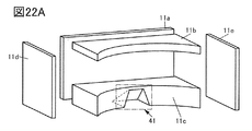
- the housing 11 can have a configuration in which a plurality of housings are connected. Examples of the configuration of the housing 11 are shown in FIGS. 22A, 22B, 22C, 23A and 23B.
- FIG. 22A shows an example in which the housing 11 has the first part 11a to the fifth part 11e.
- 22A shows a configuration in which the first portion 12a to the fifth portion 12e shown in FIGS. 4A to 4C correspond to the first part 11a to the fifth part 11e, respectively.
- the first part 11a to the fifth part 11e are connected to each other to form the housing 11. Further, any one or more of the first part 11a to the fifth part 11e may be detachable from the housing 11.
- FIG. 22B shows an example in which the housing 11 has a fourth part 11d, a fifth part 11e, and a sixth part 11f.
- FIG. 22B shows a configuration having a sixth part 11f in which the first portion 12a to the third portion 12c shown in FIGS. 4A to 4C are integrated.
- the fourth part 11d, the fifth part 11e, and the sixth part 11f are connected to each other to form the housing 11. Further, any one or more of the fourth part 11d, the fifth part 11e, and the sixth part 11f may be detachable from the housing 11.
- FIG. 22C shows an example in which the housing 11 has the first part 11a and the seventh part 11g.
- FIG. 22C shows a configuration having a seventh part 11g in which the second portion 12b to the fifth portion 12e shown in FIGS. 4A to 4C are integrated.
- the first part 11a and the seventh part 11g are connected to each other to form the housing 11. Further, any one of the first part 11a and the seventh part 11g may be detachable from the housing 11.
- FIG. 23A shows an example in which the housing 11 has a second part 11b, a third part 11c, and an eighth part 11h.
- FIG. 23A shows a configuration having an eighth part 11h in which the first portion 12a, the fourth portion 12d, and the fifth portion 12e shown in FIGS. 4A to 4C are integrated.
- the second part 11b, the third part 11c, and the eighth part 11h are connected to each other to form the housing 11. Further, any one or more of the second part 11b, the third part 11c and the eighth part 11h may be detachable from the housing 11.
- FIG. 23B shows an example in which the housing 11 has a third part 11c and a ninth part 11i.
- FIG. 23B shows a configuration having a seventh part 11g in which the first portion 12a, the second portion 12b, the fourth portion 12d, and the fifth portion 12e shown in FIGS. 4A to 4C are integrated. There is.
- the third part 11c and the ninth part 11i are connected to each other to form the housing 11. Further, any of the third part 11c and the ninth part 11i may be detachable from the housing 11.
- FIGS. 22A to 22C, 23A and 23B each part is shown separately for the sake of clarity of the figure.
- the housing 11 By connecting a plurality of parts to form the housing 11, it is possible to easily load the parts (arithmetic unit 19 and the like) provided in the electronic device 10.
- the parts are loaded into each of the first part 11a to the fifth part 11e, and then the first part 11a to the first part 11a to the first part 11a to the fifth part 11e.
- the 5 parts 11e can be connected, and the productivity can be improved as compared with the case where the first part 11a to the fifth part 11e are connected and then the parts are loaded.
- the parts can be easily replaced in the event of a failure.
- the shape of the housing 11 is not particularly limited to the shape shown in FIG. 2A and the like. Each portion constituting the housing 11 may have a curved surface. An example of the housing 11 having a curved surface is shown in FIG. 24A.
- the housing 11 has a curved surface, the design of the electronic device, which is one aspect of the present invention, can be enhanced. Further, since the housing 11 has a curved surface and the number of corners is reduced, injury can be prevented even if the user comes into contact with the housing 11, and the safety of the electronic device, which is one aspect of the present invention, can be enhanced. ..
- the electronic device may have a fixture 25 as shown in FIG. 24B.
- the housing 11 can be fixed to the user's head.
- the fixture 25 is shown in a band shape in FIG. 24B, one aspect of the present invention is not limited to this.
- FIG. 24B shows a configuration in which one end of the fixture 25 is fixed to the housing 11 by the fastener 27, another configuration may be used. For example, it may be configured without the fastener 27.
- This embodiment can be implemented by appropriately combining at least a part thereof with other embodiments described in the present specification.
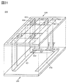
- FIG. 25 shows a block diagram showing a configuration example of a display device that can be applied to the electronic device of one aspect of the present invention.
- the display device 810 shown in FIG. 25 has a layer 820 and a layer 830 laminated above the layer 820.
- the layer 820 has a gate driver circuit 821, a source driver circuit 822, and a circuit 840.
- the layer 830 has pixels 834, and the pixels 834 are arranged in a matrix to form a pixel array 833.
- An interlayer insulator can be provided between the layer 820 and the layer 830.
- the layer 820 may be laminated above the layer 830.
- the circuit 840 is electrically connected to the source driver circuit 822.
- the circuit 840 may be electrically connected to other circuits or the like.
- Pixels 834 in the same row are electrically connected to the gate driver circuit 821 via wiring 831, and pixels 834 in the same column are electrically connected to the source driver circuit 822 via wiring 832.
- the wiring 831 has a function as a scanning line, and the wiring 832 has a function as a data line.
- FIG. 25 shows a configuration in which one row of pixels 834 is electrically connected by one wiring 831 and one row of pixels 834 is electrically connected by one wiring 832.
- one row of pixels 834 may be electrically connected by two or more wires 831 or one row of pixels 834 may be electrically connected by two or more wires 832. That is, for example, one pixel 834 may be electrically connected to two or more scanning lines, or may be electrically connected to two or more data lines.
- one wiring 831 may be electrically connected to two or more rows of pixels 834, or one wiring 832 may be electrically connected to two or more columns of pixels 834. .. That is, for example, one wiring 831 may be shared by pixels 834 having two or more rows, or one wiring 832 may be shared by pixels 834 having two or more columns.
- the gate driver circuit 821 has a function of generating a signal for controlling the operation of the pixel 834 and supplying the signal to the pixel 834 via the wiring 831.
- the source driver circuit 822 has a function of generating an image signal and supplying the signal to the pixel 834 via the wiring 832.
- the circuit 840 has, for example, a function of receiving image data that is the basis of an image signal generated by the source driver circuit 822 and supplying the received image data to the source driver circuit 822. Further, the circuit 840 has a function as a control circuit that generates a start pulse signal, a clock signal, and the like. In addition, the circuit 840 may be a circuit having a function that the gate driver circuit 821 and the source driver circuit 822 do not have.
- the pixel array 833 has a function of displaying an image corresponding to the image signal supplied to the pixel 834 by the source driver circuit 822. Specifically, an image is displayed on the pixel array 833 by emitting light having a brightness corresponding to the image signal from the pixel 834.
- the positional relationship between the layer 820 and the layer 830 is shown by a alternate long and short dash line and a white circle, and the white circles of the layer 820 and the white circles of the layer 830 overlap each other. ing. The same notation is used in other figures.
- the display device 810 has an area in which the gate driver circuit 821 and the source driver circuit 822 provided in the layer 820 overlap with the pixel array 833.
- the gate driver circuit 821 and the source driver circuit 822 have an area that overlaps with the pixel 834.
- the display device 810 can be made narrower and smaller by stacking the gate driver circuit 821, the source driver circuit 822, and the pixel array 833 so as to have regions that overlap each other. it can.
- the gate driver circuit 821 and the source driver circuit 822 are not clearly separated and have overlapping regions.
- the area is referred to as area 823.
- the region 823 By having the region 823, the occupied area of the gate driver circuit 821 and the source driver circuit 822 can be reduced. Therefore, even when the area of the pixel array 833 is small, the gate driver circuit 821 and the source driver circuit 822 can be provided without protruding from the pixel array 833.
- the area of the region of the gate driver circuit 821 and the source driver circuit 822 that does not overlap with the pixel array 833 can be reduced. From the above, the frame can be further narrowed and the size can be reduced as compared with the case where the area 823 is not provided.
- the circuit 840 can be provided so as not to overlap the pixel array 833.
- the circuit 840 may be provided so as to have a region overlapping the pixel array 833.
- FIG. 25 shows a configuration example in which one gate driver circuit 821 and one source driver circuit 822 are provided on the layer 820 and one pixel array 833 is provided on the layer 830.
- the pixel array 833 is provided on the layer 830. May be provided in plurality. That is, the pixel array provided on the layer 830 may be divided.
- FIG. 25 shows a configuration example in which the circuit 840 is provided on the layer 820, but the circuit 840 may not be provided on the layer 820.
- FIG. 26 is a modification of the configuration shown in FIG. 25, and shows a configuration example of the display device 810 when the circuit 840 is provided on the layer 830.
- the elements constituting the circuit 840 may be dispersedly provided in the layers 820 and 830.
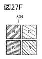
- FIG. 27A to 27E are diagrams for explaining the colors exhibited by the pixels 834 provided in the display device 810.
- a pixel 834 having a function of emitting blue light (B) are provided.
- a pixel 834 having a function of emitting cyan (C) light a pixel 834 having a function of emitting magenta (M) light, and a function of emitting yellow (Y) light.
- the pixel 834 having the above may be provided in the display device 810.
- Pixels 834 having a function of emitting white light (W) may be provided in the display device 810.
- pixel 834 having a function of emitting yellow (Y) light may be provided in the display device 810.
- a pixel 834 having a function of emitting cyan (C) light, a pixel 834 having a function of emitting magenta (M) light, and a function of emitting yellow (Y) light are provided.
- the display device 810 may be provided with a pixel 834 having a pixel 834 and a pixel 834 having a function of emitting white light (W).
- the brightness of the displayed image can be increased by providing the display device 810 with pixels 834 having a function of emitting white light (W). Further, as shown in FIG. 27D and the like, by increasing the types of colors emitted by the pixel 834, the reproducibility of intermediate colors can be improved, so that the display quality can be improved.
- the display device 810 emits pixel 834 having a function of emitting red light (R), pixel 834 having a function of emitting green light (G), and blue light (B).
- the pixel 834 having the function of emitting infrared light (IR) may be provided.
- the display device 810 has a pixel 834 having a function of emitting cyan (C) light, a pixel 834 having a function of emitting magenta (M) light, and a yellow (Y) light.
- the pixel 834 having the function of emitting infrared light (IR) may be provided.
- the display device 810 may have pixels 834 having a function of emitting white light (W) in addition to the pixels 834 shown in FIGS. 27F and 27G.
- the 28A and 28B are circuit diagrams showing a configuration example of the pixel 834.
- the pixel 834 having the configuration shown in FIG. 28A includes a transistor 552, a transistor 554, a capacitance element 562, and a light emitting device 572.
- As the light emitting device 572 for example, an EL device utilizing electroluminescence can be applied.
- the EL device has a layer containing a luminescent compound (hereinafter, also referred to as an EL layer) between a pair of electrodes. When a potential difference larger than the threshold voltage of the EL device is generated between the pair of electrodes, holes are injected into the EL layer from the anode side and electrons are injected from the cathode side. The injected electrons and holes are recombined in the EL layer, and the luminescent substance contained in the EL layer emits light.
- a luminescent compound hereinafter, also referred to as an EL layer
- EL devices are distinguished by whether the light emitting material is an organic compound or an inorganic compound, and the former is generally called an organic EL device and the latter is called an inorganic EL device.
- an organic EL device In an organic EL device, electrons are injected from one electrode and holes are injected into the EL layer from the other electrode by applying a voltage. Then, when those carriers (electrons and holes) are recombined, the luminescent organic compound forms an excited state, and when the excited state returns to the ground state, it emits light. Due to such a mechanism, such a light emitting device is called a current excitation type light emitting device.
- the EL layer is a substance having a high hole injection property, a substance having a high hole transport property, a hole blocking material, a substance having a high electron transport property, a substance having a high electron transfer property, or a bipolar. It may have a sex substance (a substance having high electron transport property and hole transport property) and the like.
- the EL layer can be formed by a vapor deposition method (including a vacuum vapor deposition method), a transfer method, a printing method, an inkjet method, a coating method, or the like.
- Inorganic EL devices are classified into dispersed inorganic EL devices and thin film type inorganic EL devices according to their device configurations.
- the dispersed inorganic EL device has a light emitting layer in which particles of a light emitting material are dispersed in a binder, and the light emitting mechanism is donor-acceptor recombination type light emission utilizing a donor level and an acceptor level.
- the thin-film inorganic EL device has a structure in which a light emitting layer is sandwiched between dielectric layers and further sandwiched between electrodes, and the light emitting mechanism is localized light emission utilizing the inner-shell electron transition of metal ions.
- the light emitting device may have at least one of a pair of electrodes transparent in order to extract light emission. Then, a transistor and a light emitting device are formed on the substrate, and a top emission (top emission) structure that extracts light emission from the surface opposite to the substrate, a bottom emission (bottom emission) structure that extracts light emission from the surface on the substrate side, and There is a double-sided emission (dual emission) light emitting device that extracts light from both sides, and any light emitting device with an injection structure can be applied.
- the same device as the light emitting device 572 can be used.
- One of the source and drain of the transistor 552 is electrically connected to the wiring 832.
- the other of the source or drain of transistor 552 is electrically connected to one electrode of the capacitive element 562 and the gate of transistor 554.
- the other electrode of the capacitive element 562 is electrically connected to the wiring 835a.
- the gate of transistor 552 is electrically connected to wiring 831.
- One of the source and drain of the transistor 554 is electrically connected to the wiring 835a.
- the other of the source or drain of the transistor 554 is electrically connected to one electrode of the light emitting device 572.
- the other electrode of the light emitting device 572 is electrically connected to the wiring 835b.
- the potential VSS is supplied to the wiring 835a
- the potential VDD is supplied to the wiring 835b.
- the wiring 835a and the wiring 835b have a function as a power supply line.
- the emission brightness from the light emitting device 572 is controlled by controlling the current flowing through the light emitting device 572 according to the potential supplied to the gate of the transistor 554.
- FIG. 28B shows a configuration different from the pixel 834 having the configuration shown in FIG. 28A.
- one of the source and the drain of the transistor 552 is electrically connected to the wiring 832.
- the other of the source or drain of transistor 552 is electrically connected to one electrode of the capacitive element 562 and the gate of transistor 554.
- the gate of transistor 552 is electrically connected to wiring 831.
- One of the source and drain of the transistor 554 is electrically connected to the wiring 835a.
- the other of the source or drain of the transistor 554 is electrically connected to the other electrode of the capacitive element 562 and one electrode of the light emitting device 572.
- the other electrode of the light emitting device 572 is electrically connected to the wiring 835b.
- the potential VDD is supplied to the wiring 835a
- the potential VSS is supplied to the wiring 835b.
- FIG. 29A is a configuration example of the pixel 834, which is different from the pixel 834 having the configuration shown in FIGS. 28A and 28B in that it has a memory.
- the pixel 834 having the configuration shown in FIG. 29A includes a transistor 511, a transistor 513, a transistor 521, a capacitive element 515, a capacitive element 517, and a light emitting device 572. Further, wiring 831_1 and wiring 831_2 are electrically connected to the pixel 834 as wiring 831 having a function as a scanning line, and wiring 832_1 and wiring 832_2 are electrically connected to the pixel 834 as wiring 832 having a function as a data line. There is.
- One of the source and drain of the transistor 511 is electrically connected to the wiring 832_1.
- the other of the source or drain of the transistor 511 is electrically connected to one electrode of the capacitive element 515.
- the gate of transistor 511 is electrically connected to wiring 831_1.
- One of the source and drain of the transistor 513 is electrically connected to the wiring 832_2.
- the other of the source or drain of the transistor 513 is electrically connected to the other electrode of the capacitive element 515.
- the gate of transistor 513 is electrically connected to wiring 831_2.
- the other electrode of the capacitive element 515 is electrically connected to one electrode of the capacitive element 517.
- One electrode of the capacitive element 517 is electrically connected to the gate of the transistor 521.
- One of the source or drain of the transistor 521 is electrically connected to one electrode of the light emitting device 572.
- the other electrode of the capacitive element 517 is electrically connected to the wiring 535.
- the other side of the source or drain of transistor 521 is electrically connected to wire 537.
- the other electrode of the light emitting device 572 is electrically connected to the wiring 539.
- the voltage supplied to the light emitting device indicates the difference between the potential applied to one electrode of the light emitting device and the potential applied to the other electrode of the light emitting device.
- Node N1 is a node in which the other electrode of the source or drain of the transistor 511 and one electrode of the capacitive element 515 are electrically connected.
- a node in which the other of the source or drain of the transistor 513, one electrode of the capacitive element 517, and the gate of the transistor 521 are electrically connected is referred to as a node N2.
- the circuit composed of the capacitance element 517, the transistor 521, and the light emitting device 572 is referred to as a circuit 401.
- the wiring 535 can be a common wiring for, for example, all the pixels 834 provided in the display device 810.
- the potential supplied to the wiring 535 is a common potential.
- a constant potential can be supplied to the wiring 537 and the wiring 539.
- the wiring 537 can be supplied with a high potential, and the wiring 539 can be supplied with a low potential.
- the wiring 537 and the wiring 539 have a function as a power supply line.
- the transistor 521 has a function of controlling the current supplied to the light emitting device 572.
- the capacitance element 517 has a function as a holding capacitance.
- the capacitive element 517 may be omitted.
- FIG. 29A shows a configuration in which the anode side of the light emitting device 572 is electrically connected to the transistor 521
- the transistor 521 may be electrically connected to the cathode side.
- the potential value of the wiring 537 and the potential value of the wiring 539 can be changed as appropriate.
- the pixel 834 can hold the potential of the node N1 by turning off the transistor 511. Further, by turning off the transistor 513, the potential of the node N2 can be maintained. Further, by turning off the transistor 513 and writing a predetermined potential to the node N1 via the transistor 511, the potential of the node N2 is changed according to the displacement of the potential of the node N1 by the capacitive coupling via the capacitive element 515. Can be made to.
- a transistor having a metal oxide in the channel forming region (hereinafter, also referred to as an OS transistor) can be applied to the transistor 511 and the transistor 513.
- the bandgap of the metal oxide can be 2 eV or more, or 2.5 eV or more. Therefore, the leakage current (off current) of the OS transistor becomes extremely small in the non-conducting state. Therefore, by applying the OS transistor to the transistor 511 and the transistor 513, the potentials of the node N1 and the node N2 can be maintained for a long period of time.
- In-M-Zn oxide (element M is aluminum, gallium, yttrium, tin, copper, vanadium, beryllium, boron, titanium, iron, nickel, germanium, zirconium, molybdenum, lantern, cerium, neodymium) , Hafnium, tantalum, tungsten, gallium, etc. (one or more) and the like may be used.
- element M aluminum, gallium, yttrium, or tin may be used.
- the metal oxide indium oxide, zinc oxide, In-Ga oxide, In-Zn oxide, Ga-Zn oxide, or gallium oxide may be used.
- FIG. 29B is a timing chart relating to the operation of the pixel 834 having the configuration shown in FIG. 29A.
- the effects of various resistors such as wiring resistance, parasitic capacitance of transistors and wiring, and the threshold voltage of transistors are not considered here.
- one frame period is divided into a period T1 and a period T2.
- the period T1 is a period for writing the potential to the node N2
- the period T2 is a period for writing the potential to the node N1.
- both the wiring 831_1 and the wiring 831_2 are supplied with a potential for turning on the transistor. Further, the potential V ref , which is a fixed potential, is supplied to the wiring 832_1, and the potential V w is supplied to the wiring 832_1.
- the potential V ref is supplied to the node N1 from the wiring 832_1 via the transistor 511. Further, the potential V w is supplied to the node N2 from the wiring 832_2 via the transistor 513. Therefore, the capacitance element 515 is in a state where the potential difference V w ⁇ V ref is held.
- the electric potential for turning on the transistor 511 is supplied to the wiring 831_1, and the potential for turning off the transistor 513 is supplied to the wiring 831_2. Further, the electric potential V data is supplied to the wiring 832_1, and a predetermined constant potential is supplied to the wiring 832_1.
- the potential of the wiring 832_2 may be floating.
- the potential V data is supplied to the node N1 via the transistor 511.
- the potential of the node N2 changes by the potential dV according to the potential V data due to the capacitive coupling by the capacitive element 515. That is, the potential obtained by adding the potential V w and the potential dV is input to the circuit 401.
- dV is shown to be a positive value in FIG. 29B, it may be a negative value. That is, the potential V data may be lower than the potential V ref.
- the potential dV is roughly determined by the capacitance value of the capacitance element 515 and the capacitance value of the circuit 401.
- the potential dV becomes a potential close to the potential difference V data ⁇ V ref.
- the image displayed on the pixel array 833 can be corrected inside the pixel 834.
- one of the two types of data signals can be the image signal described above, and the other of the two types of data signals can be, for example, a correction signal.
- the image signal can be corrected by the correction signal. Not only the image signal but also the correction signal and the like can be generated by the source driver circuit 822 of the display device 810.
- the pixel 834 having the configuration shown in FIG. 29A can have the potential of the node N2 exceeding the maximum potential that can be supplied to the wiring 832_1 and the wiring 832_2.
- a high voltage can be supplied to the light emitting device 572.
- the potential of the wiring 537 can be increased. Therefore, when the light emitting device 572 is an organic EL device, the light emitting device can have a tandem structure described later. Thereby, the current efficiency and the external quantum efficiency of the light emitting device 572 can be increased. Therefore, a high-luminance image can be displayed on the display device 810. In addition, the power consumption of the display device 810 can be reduced.
- the circuit is not limited to the circuit illustrated in FIG. 29A, and a transistor, a capacitive element, or the like may be added separately.
- the number of nodes capable of holding the potential can be increased to three. That is, another node capable of holding the potential can be provided in the pixel 834 in addition to the node N1 and the node N2.
- the potential of the node N2 can be further increased. Therefore, a larger current can be passed through the light emitting device 572.
- FIGS. 30A to 30E are diagrams showing a configuration example of a circuit 401 different from that of FIG. 30A.
- the circuit 401 having the configuration shown in FIG. 30A has a capacitance element 517, a transistor 521, and a light emitting device 572, similarly to the circuit 401 having the configuration shown in FIG. 29A.
- the gate of the transistor 521 and one electrode of the capacitive element 517 are electrically connected to the node N2.
- One of the source and drain of the transistor 521 is electrically connected to the wiring 537.
- the other of the source or drain of the transistor 521 is electrically connected to the other electrode of the capacitive element 517.
- the other electrode of the capacitive element 517 is electrically connected to one electrode of the light emitting device 572.
- the other electrode of the light emitting device 572 is electrically connected to the wiring 539.
- the circuit 401 having the configuration shown in FIG. 30B also has a capacitance element 517, a transistor 521, and a light emitting device 572, similarly to the circuit 401 having the configuration shown in FIG. 29A.
- the gate of the transistor 521 and one electrode of the capacitive element 517 are electrically connected to the node N2.
- One electrode of the light emitting device 572 is electrically connected to the wiring 537.
- the other electrode of the light emitting device 572 is electrically connected to one of the source or drain of the transistor 521.
- the other of the source or drain of the transistor 521 is electrically connected to the other electrode of the capacitive element 517.
- the other electrode of the capacitive element 517 is electrically connected to the wiring 539.
- FIG. 30C shows a configuration example of the circuit 401 when the transistor 525 is added to the circuit 401 shown in FIG. 30A.
- One of the source or drain of the transistor 525 is electrically connected to the other of the source or drain of the transistor 521 and the other electrode of the capacitive element 517.
- the other of the source or drain of the transistor 525 is electrically connected to one electrode of the light emitting device 572.
- the gate of transistor 525 is electrically connected to wiring 541.
- the wiring 541 has a function as a scanning line for controlling the continuity of the transistor 525.
- FIG. 30D shows a configuration example of the circuit 401 when the transistor 527 is added to the circuit 401 shown in FIG. 30C.
- One of the source or drain of transistor 527 is electrically connected to the other of the source or drain of transistor 521.
- the other of the source or drain of transistor 527 is electrically connected to wire 543.
- the gate of transistor 527 is electrically connected to wiring 545.
- the wiring 545 has a function as a scanning line for controlling the continuity of the transistor 527.
- the wiring 543 can be electrically connected to a supply source of a specific potential such as a reference potential. That is, the wiring 543 has a function as a power supply line. By supplying a specific potential from the wiring 543 to the other of the source or drain of the transistor 521, it is possible to stabilize the writing of the image signal to the pixel 834.
- Wiring 543 can be electrically connected to circuit 520.
- the circuit 520 can have one or more of the above-mentioned specific potential supply source, a function of acquiring the electrical characteristics of the transistor 521, and a function of generating a correction signal.
- the circuit 401 having the configuration shown in FIG. 30E includes a capacitance element 517, a transistor 521, a transistor 529, and a light emitting device 572.
- the gate of the transistor 521 and one electrode of the capacitive element 517 are electrically connected to the node N2.
- One of the source and drain of the transistor 521 is electrically connected to the wiring 537.
- One of the source or drain of the transistor 529 is electrically connected to the wiring 543.
- the other electrode of the capacitive element 517 is electrically connected to the other of the source or drain of the transistor 521.
- the other of the source or drain of transistor 521 is electrically connected to the other of the source or drain of transistor 529.
- the other of the source or drain of the transistor 529 is electrically connected to one electrode of the light emitting device 572.
- the gate of the transistor 529 is electrically connected to the wiring 831_1.
- the other electrode of the light emitting device 572 is electrically connected to the wiring 539.
- FIG. 31 is a block diagram showing a configuration example of the display device 810 when the pixel 834 has the configuration shown in FIG. 29A.
- the display device 810 having the configuration shown in FIG. 31 is provided with a demultiplexer circuit 824 in addition to the components of the display device 810 shown in FIG. 25.
- the demultiplexer circuit 824 can be provided, for example, in layer 820, as shown in FIG.
- the number of demultiplexer circuits 824 can be, for example, the same as the number of columns of pixels 834 provided in the pixel array 833.
- the gate driver circuit 821 is electrically connected to the pixel 834 via the wiring 831-1.
- the gate driver circuit 821 is electrically connected to the pixel 834 via wiring 831-2.
- the wiring 831-1 and the wiring 831-2 have a function as scanning lines.
- the source driver circuit 822 is electrically connected to the input terminal of the demultiplexer circuit 824.
- the first output terminal of the demultiplexer circuit 824 is electrically connected to the pixel 834 via the wiring 832-1.
- the second output terminal of the demultiplexer circuit 824 is electrically connected to the pixel 834 via the wiring 832-2.
- the wiring 832-1 and the wiring 832-2 have a function as a data line.
- the source driver circuit 822 and the demultiplexer circuit 824 may be collectively referred to as a source driver circuit. That is, the demultiplexer circuit 824 may be included in the source driver circuit 822.
- the source driver circuit 822 has a function of generating the image signal S1 and the image signal S2.
- the demultiplexer circuit 824 has a function of supplying the image signal S1 to the pixel 834 via the wiring 832-1 and a function of supplying the image signal S2 to the pixel 834 via the wiring 832-2.
- the potential V data can be set to the potential corresponding to the image signal S1
- the potential V w corresponds to the image signal S2. Can be the potential to be.
- the potential of the node N2 becomes “V w + dV”.
- the potential dV is the potential corresponding to the potential V data. Therefore, the image signal S1 can be added to the image signal S2. That is, the image signal S1 can be superimposed on the image signal S2.
- the magnitudes of the potential V data corresponding to the image signal S1 and the potential V w corresponding to the image signal S2 are limited according to the withstand voltage of the source driver circuit 822 and the like. Therefore, by superimposing the image signal S1 and the image signal S2, an image corresponding to the image signal having a potential higher than the potential that can be output by the source driver circuit 822 can be displayed on the pixel array 833. As a result, a large current can be passed through the light emitting device 572, so that a high-luminance image can be displayed on the pixel array 833.
- the dynamic range which is the range of brightness of the image that can be displayed by the pixel array 833, can be expanded.
- the image corresponding to the image signal S1 and the image corresponding to the image signal S2 may be the same or different.
- the pixel array 833 has the brightness of the image corresponding to the image signal S1 and the brightness of the image corresponding to the image signal S2. An image with higher brightness can be displayed.
- FIG. 32 shows a case where the image P1 corresponding to the image signal S1 contains only characters and the image P2 corresponding to the image signal S2 contains a picture and characters.
- the brightness of the characters can be increased, and for example, the characters can be emphasized.
- FIG. 29B after the potential V w is written to the node N2, the potential of the node N2 changes according to the potential V data. Therefore, when rewriting the potential V w corresponding to the image signal S2, , The potential V data of the image signal S1 must be written again.
- the image P2 is an image that is rewritten less frequently than the image P1.
- FIG. 32 shows an example in which the image P1 contains only characters and the image P2 contains pictures and characters, one aspect of the present invention is not limited to this.
- FIG. 33 is a cross-sectional view showing a configuration example of the display device 810.
- the display device 810 has a substrate 701 and a substrate 705, and the substrate 701 and the substrate 705 are bonded to each other by a sealing material 712.
- a single crystal semiconductor substrate such as a single crystal silicon substrate can be used.
- a semiconductor substrate other than the single crystal semiconductor substrate may be used as the substrate 701.
- a transistor 441 and a transistor 601 are provided on the substrate 701.
- the transistor 441 can be a transistor provided in the circuit 840.
- the transistor 601 can be a transistor provided in the gate driver circuit 821 or a transistor provided in the source driver circuit 822. That is, the transistor 441 and the transistor 601 can be provided on the layer 820 shown in FIG. 25 and the like.
- the transistor 441 is composed of a conductor 443 having a function as a gate electrode, an insulator 445 having a function as a gate insulator, and a part of a substrate 701, and is a semiconductor region 447 including a channel forming region and a source region. Alternatively, it has a low resistance region 449a that functions as one of the drain regions and a low resistance region 449b that functions as the other of the source region or the drain region.
- the transistor 441 may be either a p-channel type or an n-channel type.
- the transistor 441 is electrically separated from other transistors by the element separation layer 403.
- FIG. 33 shows a case where the transistor 441 and the transistor 601 are electrically separated by the element separation layer 403.
- the element separation layer 403 can be formed by using a LOCOS (LOCOxidation of Silicon) method, an STI (Shallow Trench Isolation) method, or the like.
- the semiconductor region 447 has a convex shape. Further, the side surface and the upper surface of the semiconductor region 447 are provided so as to be covered with the conductor 443 via the insulator 445. Note that FIG. 33 does not show how the conductor 443 covers the side surface of the semiconductor region 447. Further, a material for adjusting the work function can be used for the conductor 443.
- a transistor having a convex shape in the semiconductor region such as the transistor 441 can be called a fin type transistor because the convex portion of the semiconductor substrate is used.
- an insulator which is in contact with the upper part of the convex portion and has a function as a mask for forming the convex portion may be provided.
- FIG. 33 shows a configuration in which a part of the substrate 701 is processed to form a convex portion, the SOI substrate may be processed to form a semiconductor having a convex shape.
- the configuration of the transistor 441 shown in FIG. 33 is an example, and is not limited to the configuration, and may be an appropriate configuration according to the circuit configuration, the operation method of the circuit, and the like.
- the transistor 441 may be a planar transistor.
- the transistor 601 can have the same configuration as the transistor 441.
- an insulator 405, an insulator 407, an insulator 409, and an insulator 411 are provided.
- the conductor 451 is embedded in the insulator 405, the insulator 407, the insulator 409, and the insulator 411.
- the height of the upper surface of the conductor 451 and the height of the upper surface of the insulator 411 can be made about the same.
- Insulator 413 and insulator 415 are provided on the conductor 451 and the insulator 411. Further, the conductor 457 is embedded in the insulator 413 and the insulator 415.
- Insulator 417 and insulator 419 are provided on the conductor 457 and the insulator 415. Further, the conductor 459 is embedded in the insulator 417 and the insulator 419.
- Insulator 421 and insulator 214 are provided on the conductor 459 and the insulator 419.
- the conductor 453 is embedded in the insulator 421 and in the insulator 214.
- the height of the upper surface of the conductor 453 and the height of the upper surface of the insulator 214 can be made about the same.
- Insulator 216 is provided on the conductor 453 and on the insulator 214.
- a conductor 455 is embedded in the insulator 216.
- the height of the upper surface of the conductor 455 and the height of the upper surface of the insulator 216 can be made about the same.
- Insulator 222, insulator 224, insulator 254, insulator 244, insulator 280, insulator 274, and insulator 281 are provided on the conductor 455 and the insulator 216.
- the conductor 305 is embedded in the insulator 222, the insulator 224, the insulator 254, the insulator 244, the insulator 280, the insulator 274, and the insulator 281.
- the height of the upper surface of the conductor 305 and the height of the upper surface of the insulator 281 can be made about the same.
- the insulator 361 is provided on the conductor 305 and the insulator 281.
- a conductor 317 and a conductor 337 are embedded in the insulator 361.
- the height of the upper surface of the conductor 337 and the height of the upper surface of the insulator 361 can be made about the same.
- the insulator 363 is provided on the conductor 337 and the insulator 361.
- a conductor 347, a conductor 353, a conductor 355, and a conductor 357 are embedded in the insulator 363.
- the height of the upper surface of the conductor 353, the conductor 355, and the conductor 357 can be made the same as the height of the upper surface of the insulator 363.
- connection electrode 760 is provided on the conductor 353, the conductor 355, the conductor 357, and the insulator 363. Further, an anisotropic conductor 780 is provided so as to be electrically connected to the connection electrode 760, and an FPC (Flexible Printed Circuit) 716 is provided so as to be electrically connected to the anisotropic conductor 780.
- FPC Flexible Printed Circuit
- the low resistance region 449b having a function as the other of the source region and the drain region of the transistor 441 includes a conductor 451 and a conductor 457, a conductor 459, a conductor 453, a conductor 455, and a conductor. It is electrically connected to the FPC 716 via 305, conductor 317, conductor 337, conductor 347, conductor 353, conductor 355, conductor 357, connection electrode 760, and anisotropic conductor 780. ..
- connection electrode 760 and the conductor 347 shows three conductors having a function of electrically connecting the connection electrode 760 and the conductor 347, that is, the conductor 353, the conductor 355, and the conductor 357, which is one of the present inventions.
- the aspect is not limited to this.
- the number of conductors having a function of electrically connecting the connection electrode 760 and the conductor 347 may be one, two, or four or more.
- the contact resistance can be reduced by providing a plurality of conductors having a function of electrically connecting the connection electrode 760 and the conductor 347.
- a transistor 750 is provided on the insulator 214.
- the transistor 750 can be a transistor provided in the pixel 834. That is, the transistor 750 can be provided on the layer 830 shown in FIG. 25 and the like.
- an OS transistor can be used as the transistor 750.
- the OS transistor has a feature that the off-current is extremely low. Therefore, since the holding time of the image signal or the like can be lengthened, the frequency of the refresh operation can be reduced. Therefore, the power consumption of the display device 810 can be reduced.
- Conductors 301a and 301b are embedded in the insulator 254, the insulator 244, the insulator 280, the insulator 274, and the insulator 281.
- the conductor 301a is electrically connected to one of the source or drain of the transistor 750
- the conductor 301b is electrically connected to the other of the source or drain of the transistor 750.
- the height of the upper surfaces of the conductors 301a and 301b and the height of the upper surfaces of the insulator 281 can be made about the same.
- a conductor 311, a conductor 313, a conductor 331, a capacitance element 790, a conductor 333, and a conductor 335 are embedded in the insulator 361.
- the conductors 311 and 313 are electrically connected to the transistor 750 and have a function as wiring.
- the conductor 333 and the conductor 335 are electrically connected to the capacitive element 790.
- the height of the upper surface of the conductor 331, the conductor 333, and the conductor 335 can be made the same as the height of the upper surface of the insulator 361.
- Conductor 341, conductor 343, and conductor 351 are embedded in the insulator 363.
- the height of the upper surface of the conductor 351 and the height of the upper surface of the insulator 363 can be made about the same.
- the 281, the insulator 361, and the insulator 363 have a function as an interlayer film, and may have a function as a flattening film that covers the uneven shape below each of them.
- the upper surface of the insulator 363 may be flattened by a flattening treatment using a chemical mechanical polishing (CMP) method or the like in order to improve the flatness.
- CMP chemical mechanical polishing
- the capacitive element 790 has a lower electrode 321 and an upper electrode 325. Further, an insulator 323 is provided between the lower electrode 321 and the upper electrode 325. That is, the capacitive element 790 has a laminated structure in which an insulator 323 that functions as a dielectric is sandwiched between a pair of electrodes.
- FIG. 33 shows an example in which the capacitance element 790 is provided on the insulator 281, the capacitance element 790 may be provided on an insulator different from the insulator 281.
- FIG. 33 shows an example in which the conductor 301a, the conductor 301b, and the conductor 305 are formed in the same layer. Further, an example is shown in which the conductor 311 and the conductor 313, the conductor 317, and the lower electrode 321 are formed in the same layer. Further, an example is shown in which the conductor 331, the conductor 333, the conductor 335, and the conductor 337 are formed in the same layer. Further, an example is shown in which the conductor 341, the conductor 343, and the conductor 347 are formed in the same layer. Further, an example is shown in which the conductor 351 and the conductor 353, the conductor 355, and the conductor 357 are formed in the same layer.
- the display device 810 shown in FIG. 33 has a light emitting device 572.
- the light emitting device 572 has a conductor 772, an EL layer 786, and a conductor 788.
- the conductor 788 is provided on the substrate 705 side and has a function as a common electrode. Further, the conductor 772 is electrically connected to the other of the source or drain of the transistor 750 via the conductor 351 and the conductor 341, the conductor 331, the conductor 313, and the conductor 301b.
- the conductor 772 is formed on the insulator 363 and has a function as a pixel electrode. Further, the EL layer 786 has an organic compound or an inorganic compound such as a quantum dot.
- Examples of materials that can be used for organic compounds include fluorescent materials and phosphorescent materials.
- Examples of materials that can be used for quantum dots include colloidal quantum dot materials, alloy-type quantum dot materials, core-shell type quantum dot materials, and core-type quantum dot materials.
- an insulator 730 is provided on the insulator 363.
- the insulator 730 can be configured to cover a part of the conductor 772.
- the light emitting device 572 has a translucent conductor 788, and can be a top emission type light emitting device.
- the light emitting device 572 may have a bottom emission structure that emits light to the conductor 772 side, or a dual emission structure that emits light to both the conductor 772 and the conductor 788.
- the light emitting device 572 can have a microcavity structure, which will be described in detail later.
- a predetermined color for example, RGB
- the display device 810 can perform color display.
- the display device 810 can display a high-brightness image, and the power consumption of the display device 810 can be reduced.
- the EL layer 786 is formed in an island shape for each pixel or in a striped shape for each pixel row, that is, when the EL layer 786 is formed by painting separately, it is possible to configure the structure without providing the colored layer.
- the light-shielding layer 738 is provided so as to have a region overlapping with the insulator 730. Further, the light-shielding layer 738 is covered with an insulator 734. Further, the space between the light emitting device 572 and the insulator 734 is filled with a sealing layer 732.
- a structure 778 is provided between the insulator 730 and the EL layer 786. Further, a structure 778 is provided between the insulator 730 and the insulator 734.
- the structure 778 is a columnar spacer and has a function of controlling the distance (cell gap) between the substrate 701 and the substrate 705.
- a spherical spacer may be used as the structure 778.
- a light-shielding layer 738 and an insulator 734 in contact with the light-shielding layer 738 are provided on the substrate 705 side.
- the light-shielding layer 738 has a function of blocking light emitted from an adjacent region.
- the light-shielding layer 738 has a function of blocking external light from reaching the transistor 750 or the like.
- FIG. 34 is a modified example of the display device 810 shown in FIG. 33, and is different from the display device 810 shown in FIG. 33 in that a colored layer 736 is provided.
- the colored layer 736 By providing the colored layer 736, the color purity of the light extracted from the light emitting device 572 can be increased. As a result, a high-quality image can be displayed on the display device 810.
- all the light emitting devices 572 of the display device 810 can be light emitting devices that emit white light, so that the EL layer 786 does not have to be formed by painting separately, and the display device 810 has a high definition. can do.
- FIGS. 33 and 34 the transistor 441 and the transistor 601 are provided so as to form a channel forming region inside the substrate 701, and the OS transistor is provided by laminating the transistor 441 and the transistor 601.
- FIG. 35 is a modification of FIG. 33
- FIG. 36 is a modification of FIG. 34, in which the transistor 750 is provided by being laminated on the OS transistors 602 and 603 instead of the transistor 441 and the transistor 601.
- the display device 810 having the configuration shown in FIGS. 33 and 34 is provided with OS transistors stacked.
- An insulator 613 and an insulator 614 are provided on the substrate 701, and a transistor 602 and a transistor 603 are provided on the insulator 614.
- a transistor or the like may be provided between the substrate 701 and the insulator 613.
- a transistor having the same configuration as the transistor 441 and the transistor 601 shown in FIGS. 33 and 34 may be provided between the substrate 701 and the insulator 613.
- the transistor 602 can be a transistor provided in the circuit 840.
- the transistor 603 can be a transistor provided in the gate driver circuit 821 or a transistor provided in the source driver circuit 822. That is, the transistor 602 and the transistor 603 can be provided on the layer 820 shown in FIG. 25 and the like. As shown in FIG. 26, when the circuit 840 is provided on the layer 830, the transistor 602 can be provided on the layer 830.
- the transistor 602 and the transistor 603 can be a transistor having the same configuration as the transistor 750.
- the transistor 602 and the transistor 603 may be OS transistors having a configuration different from that of the transistor 750.
- an insulator 616, an insulator 622, an insulator 624, an insulator 654, an insulator 644, an insulator 680, an insulator 674, and an insulator 681 are provided on the insulator 614. ..
- the conductor 461 is embedded in the insulator 654, the insulator 644, the insulator 680, the insulator 674, and the insulator 681.
- the height of the upper surface of the conductor 461 and the height of the upper surface of the insulator 681 can be made about the same.
- the insulator 501 is provided on the conductor 461 and the insulator 681.
- a conductor 463 is embedded in the insulator 501.
- the height of the upper surface of the conductor 463 and the height of the upper surface of the insulator 501 can be made about the same.
- the insulator 503 is provided on the conductor 463 and the insulator 501.
- a conductor 465 is embedded in the insulator 503.
- the height of the upper surface of the conductor 465 and the height of the upper surface of the insulator 503 can be made about the same.
- the insulator 505 is provided on the conductor 465 and the insulator 503. Further, the conductor 467 is embedded in the insulator 505.
- the insulator 507 is provided on the conductor 467 and the insulator 505.
- a conductor 469 is embedded in the insulator 507.
- the height of the upper surface of the conductor 469 and the height of the upper surface of the insulator 507 can be made about the same.
- the insulator 509 is provided on the conductor 469 and the insulator 507. Further, the conductor 471 is embedded in the insulator 509.
- Insulator 421 and insulator 214 are provided on the conductor 471 and the insulator 509.
- the conductor 453 is embedded in the insulator 421 and in the insulator 214.
- the height of the upper surface of the conductor 453 and the height of the upper surface of the insulator 214 can be made about the same.
- one of the source or drain of the transistor 602 is a conductor 461, a conductor 463, a conductor 465, a conductor 467, a conductor 469, a conductor 471, a conductor 453, or a conductor. Electrically with FPC716 via 455, conductor 305, conductor 317, conductor 337, conductor 347, conductor 353, conductor 355, conductor 357, connection electrode 760, and anisotropic conductor 780. It is connected.
- the insulator 613, the insulator 614, the insulator 680, the insulator 674, the insulator 681, the insulator 501, the insulator 503, the insulator 505, the insulator 507, and the insulator 509 have a function as an interlayer film. , It may have a function as a flattening film that covers each of the lower uneven shapes.
- the display device 810 By configuring the display device 810 as shown in FIGS. 35 and 36, all the transistors of the display device 810 can be used as OS transistors while the display device 810 is narrowed and downsized. Thereby, for example, the transistor provided in the layer 820 and the transistor provided in the layer 830 can be manufactured by using the same device. Therefore, the manufacturing cost of the display device 810 can be reduced, and the display device 810 can be made inexpensive.
- FIG. 37A to 37E are diagrams showing a configuration example of the light emitting device 572.
- FIG. 37A shows a structure (single structure) in which the EL layer 786 is sandwiched between the conductor 772 and the conductor 788.
- the EL layer 786 contains a light emitting material, for example, a light emitting material which is an organic compound.
- FIG. 37B is a diagram showing a laminated structure of EL layer 786.
- the conductor 772 has a function as an anode
- the conductor 788 has a function as a cathode.
- the EL layer 786 has a structure in which the hole injection layer 721, the hole transport layer 722, the light emitting layer 723, the electron transport layer 724, and the electron injection layer 725 are sequentially laminated on the conductor 772.
- the conductor 772 has a function as a cathode and the conductor 788 has a function as an anode, the stacking order is reversed.
- the light emitting layer 723 has a light emitting material or a plurality of materials in an appropriate combination, and can be configured to obtain fluorescent light emission or phosphorescent light emission exhibiting a desired light emitting color. Further, the light emitting layer 723 may have a laminated structure having different light emitting colors. In this case, different materials may be used for the luminescent substance and other substances used for each of the laminated light emitting layers.
- the conductor 772 shown in FIG. 37B is used as a reflecting electrode
- the conductor 788 is used as a semi-transmissive / semi-reflective electrode
- the EL layer 786 has a micro-optical resonator (microcavity) structure.
- the light emitted from the light emitting layer 723 can be resonated between both electrodes to enhance the light emitted through the conductor 788.
- the conductor 772 of the light emitting device 572 is a reflective electrode having a laminated structure of a conductive material having a reflective property and a conductive material having a translucent property (transparent conductive film)
- the thickness of the transparent conductive film is formed.
- Optical adjustment can be performed by controlling. Specifically, the distance between the electrodes of the conductor 772 and the conductor 788 is adjusted to be close to m ⁇ / 2 (where m is a natural number) with respect to the wavelength ⁇ of the light obtained from the light emitting layer 723. Is preferable.
- the light emitting region referred to here means a recombination region of holes and electrons in the light emitting layer 723.
- the spectrum of a specific monochromatic light obtained from the light emitting layer 723 can be narrowed, and light emission with good color purity can be obtained.
- the optical distance between the conductor 772 and the conductor 788 can be said to be strictly the total thickness from the reflection region of the conductor 772 to the reflection region of the conductor 788.
- the above-mentioned effect can be sufficiently obtained by assuming an arbitrary position of the conductor 772 and the conductor 788 as the reflection region. It shall be possible.
- the optical distance between the conductor 772 and the light emitting layer from which the desired light can be obtained is, strictly speaking, the optical distance between the reflection region of the conductor 772 and the light emitting region in the light emitting layer where the desired light can be obtained. be able to.
- the reflection region and the desired light can be obtained at an arbitrary position of the conductor 772. It is assumed that the above-mentioned effect can be sufficiently obtained by assuming that an arbitrary position of the light emitting layer is a light emitting region.
- the light emitting device 572 shown in FIG. 37B has a microcavity structure, it is possible to extract light of different wavelengths (monochromatic light) even if it has the same EL layer. Therefore, it is not necessary to separately paint (for example, RGB) to obtain different emission colors. Therefore, it is easy to realize high definition. It can also be combined with a colored layer. Further, since it is possible to increase the emission intensity in the front direction of a specific wavelength, it is possible to reduce the power consumption.
- the light emitting device 572 shown in FIG. 37B does not have to have a microcavity structure.
- the light emitting layer 723 has a structure that emits white light, and by providing the colored layer, light of a predetermined color (for example, RGB) can be extracted. Further, when forming the EL layer 786, if different coatings are performed to obtain different emission colors, light of a predetermined color can be taken out without providing a colored layer.
- At least one of the conductor 772 and the conductor 788 can be a translucent electrode (transparent electrode, semi-transmissive / semi-reflective electrode, etc.).
- the electrode having translucency is a transparent electrode
- the transmittance of visible light of the transparent electrode is 40% or more.
- the reflectance of visible light of the semi-transmissive / semi-reflective electrode is 20% or more and 80% or less, preferably 40% or more and 70% or less.
- the resistivity of these electrodes is preferably 1 ⁇ 10 -2 ⁇ cm or less.
- the visible light reflectance of the reflective electrode is 40% or more and 100% or less, preferably 70% or more and 100% or less. And.
- the resistivity of this electrode is preferably 1 ⁇ 10 -2 ⁇ cm or less.
- the configuration of the light emitting device 572 may be the configuration shown in FIG. 37C.
- two EL layers (EL layer 786a and EL layer 786b) are provided between the conductor 772 and the conductor 788, and a charge generation layer 792 is provided between the EL layer 786a and the EL layer 786b.
- the light emitting device 572 having a laminated structure (tandem structure) is shown.
- the current efficiency and the external quantum efficiency of the light emitting device 572 can be improved. Therefore, a high-luminance image can be displayed on the display device 810.
- the power consumption of the display device 810 can be reduced.
- the EL layer 786a and the EL layer 786b can have the same configuration as the EL layer 786 shown in FIG. 37B.
- the charge generation layer 792 injects electrons into one of the EL layer 786a and the EL layer 786b, and injects holes into the other.
- the charge generation layer 792 injects electrons into one of the EL layer 786a and the EL layer 786b, and injects holes into the other.
- a voltage is supplied so that the potential of the conductor 772 is higher than the potential of the conductor 788, electrons are injected from the charge generation layer 792 into the EL layer 786a, and holes are injected from the charge generation layer 792 into the EL layer 786b. Will be done.
- the charge generation layer 792 preferably transmits visible light (specifically, the visible light transmittance of the charge generation layer 792 is 40% or more) from the viewpoint of light extraction efficiency. Further, the conductivity of the charge generation layer 792 may be lower than the conductivity of the conductor 772 or the conductivity of the conductor 788.
- the configuration of the light emitting device 572 may be the configuration shown in FIG. 37D.
- three EL layers (EL layer 786a, EL layer 786b, and EL layer 786c) are provided between the conductor 772 and the conductor 788, and between the EL layer 786a and the EL layer 786b, A tandem-structured light emitting device 572 having a charge generation layer 792 between the EL layer 786b and the EL layer 786c is shown.
- the EL layer 786a, the EL layer 786b, and the EL layer 786c can have the same configuration as the EL layer 786 shown in FIG. 37B.
- the configuration of the light emitting device 572 may be the configuration shown in FIG. 37E.
- n layers of EL layers (EL layers 786 (1) to EL layers 786 (n)) are provided between the conductor 772 and the conductor 788, and electric charges are generated between the respective EL layers 786.
- the tandem structure light emitting device 572 having the layer 792 is shown.
- the EL layer 786 (1) to the EL layer 786 (n) can have the same configuration as the EL layer 786 shown in FIG. 37B.
- FIG. 37E shows the EL layer 786 (1), the EL layer 786 (m), the EL layer 786 (m + 1), and the EL layer 786 (n) among the EL layers 786.
- n is an integer greater than m.
- n is an integer greater than m.
- Conductor 772 and Conductor 788 The following materials can be appropriately combined and used for the conductor 772 and the conductor 788 as long as the functions of the anode and the cathode can be satisfied.
- metals, alloys, electrically conductive compounds, mixtures thereof, and the like can be appropriately used. Specific examples thereof include In—Sn oxide (also referred to as ITO), In—Si—Sn oxide (also referred to as ITSO), In—Zn oxide, and In—W—Zn oxide.
- Other elements belonging to Group 1 or Group 2 of the Periodic Table of Elements eg, Lithium (Li), Cesium (Cs), Calcium (Ca), Strontium (Sr)), Europium (Eu), Ytterbium Rare earth metals such as (Yb), alloys containing these in appropriate combinations, and other graphenes can be used.
- the hole injection layer 721 is a layer for injecting holes into the EL layer 786 from the conductor 772 which is an anode or the charge generation layer 792, and is a layer containing a material having a high hole injection property.
- the EL layer 786 includes an EL layer 786a, an EL layer 786b, an EL layer 786c, and an EL layer 786 (1) to an EL layer 786 (n).
- materials with high hole injection properties include transition metal oxides such as molybdenum oxide, vanadium oxide, ruthenium oxide, tungsten oxide, and manganese oxide.
- transition metal oxides such as molybdenum oxide, vanadium oxide, ruthenium oxide, tungsten oxide, and manganese oxide.
- phthalocyanine compounds, aromatic amine compounds, polymer compounds and the like can be used.
- a composite material containing a hole transporting material and an acceptor material can also be used.
- electrons are extracted from the hole transporting material by the acceptor material, holes are generated in the hole injection layer 721, and holes are injected into the light emitting layer 723 via the hole transport layer 722.
- the hole injection layer 721 may be formed of a single layer composed of a composite material containing a hole transporting material and an acceptor material (electron acceptor material), but the hole transporting material and the acceptor material (acceptor material) may be formed.
- the electron acceptor material may be laminated and formed in separate layers.
- the hole transport layer 722 is a layer that transports the holes injected from the conductor 772 to the light emitting layer 723 by the hole injection layer 721.
- the hole transport layer 722 is a layer containing a hole transport material.
- oxides of metals belonging to Groups 4 to 8 in the Periodic Table of the Elements can be used. Specific examples thereof include molybdenum oxide, vanadium oxide, niobium oxide, tantalum oxide, chromium oxide, tungsten oxide, manganese oxide and renium oxide. Of these, molybdenum oxide is particularly preferable because it is stable in the atmosphere, has low hygroscopicity, and is easy to handle.
- organic acceptors such as quinodimethane derivatives, chloranil derivatives, and hexaazatriphenylene derivatives can be used.
- hole-transporting material used for the hole-injecting layer 721 and the hole-transporting layer 722 a material having a hole mobility of 10-6 cm 2 / Vs or more is preferable. Any substance other than these can be used as long as it is a substance having a higher hole transport property than electrons.
- a ⁇ -electron-rich heteroaromatic compound for example, a carbazole derivative or an indole derivative
- an aromatic amine compound for example, a compound having an aromatic amine skeleton, a compound having a carbazole skeleton, a compound having a thiophene skeleton, and a compound having a furan skeleton can be used.
- a polymer compound can also be used as the hole transporting material.
- the hole transporting material is not limited to the above, and various known materials can be used as the hole transporting material for the hole injection layer 721 and the hole transporting layer 722 by combining one or a plurality of known materials. ..
- the hole transport layer 722 may be formed of a plurality of layers. That is, in the hole transport layer 722, for example, the first hole transport layer and the second hole transport layer may be laminated.
- the light emitting layer 723 is a layer containing a light emitting substance.
- a substance exhibiting a luminescent color such as blue, purple, bluish purple, green, yellowish green, yellow, orange, and red is appropriately used.
- FIGS. 37C, 37D, and (E) when the light emitting device 572 has a plurality of EL layers, different light emitting substances are used for the light emitting layer 723 provided in each EL layer to emit different light. It can be configured to exhibit a color (for example, white emission obtained by combining emission colors having a complementary color relationship). For example, when the light emitting device 572 has the configuration shown in FIG.
- the light emitting substance used for the light emitting layer 723 provided on the EL layer 786a and the light emitting substance used for the light emitting layer 723 provided on the EL layer 786b are made different from each other. Thereby, the emission color exhibited by the EL layer 786a and the emission color exhibited by the EL layer 786b can be made different from each other.
- one light emitting layer may have a laminated structure having different light emitting substances.
- the light emitting layer 723 may have one or more kinds of organic compounds (host material, assist material) in addition to the light emitting substance (guest material). Further, one or both of the hole transporting material and the electron transporting material can be used as one or more kinds of organic compounds.
- a light emitting substance blue light emitting substance that emits blue light is used as a guest material in either one of the EL layer 786a and the EL layer 786b, and a substance that emits green light in the other. It is preferable to use (green luminescent substance) and a substance exhibiting red luminescence (red luminescent substance). This method is effective when the luminous efficiency and life of the blue light emitting substance (blue light emitting layer) are inferior to those of others.
- a luminescent material that converts singlet excitation energy into light emission in the visible light region is used as the blue luminescent material
- a luminescent material that converts triplet excitation energy into light emission in the visible light region is used as the green and red luminescent material. This is preferable because it improves the spectral balance of RGB.
- the luminescent material that can be used for the light emitting layer 723 is not particularly limited, and a luminescent material that converts singlet excitation energy into light emission in the visible light region or a luminescent material that converts triplet excitation energy into light emission in the visible light region is used. Can be done. Examples of the luminescent substance include the following.
- luminescent substances that convert single-term excitation energy into luminescence include substances that emit fluorescence (fluorescent materials).
- fluorescent materials include substances that emit fluorescence (fluorescent materials).
- fluorescent materials include substances that emit fluorescence (fluorescent materials).
- fluorescent materials include substances that emit fluorescence (fluorescent materials).
- fluorescent materials include substances that emit fluorescence (fluorescent materials).
- fluorescent materials include fluorescence (fluorescent materials).
- fluorescence fluorescence (fluorescent materials).
- fluorescence fluorescence
- pyrene derivatives anthracene derivatives, triphenylene derivatives, fluorene derivatives, carbazole derivatives, dibenzothiophene derivatives, dibenzofuran derivatives, and dibenzoquinoxalin.
- examples thereof include derivatives, quinoxalin derivatives, pyridine derivatives, pyrimidine derivatives, phenanthrene derivatives, naphthalene derivatives and the like
- Examples of the luminescent substance that converts triplet excitation energy into light emission include a substance that emits phosphorescence (phosphorescent material) and a thermally activated delayed fluorescence (TADF) material that exhibits thermal activated delayed fluorescence.
- phosphorescent material phosphorescent material
- TADF thermally activated delayed fluorescence
- the phosphorescent material examples include an organic metal complex, a metal complex (platinum complex), and a rare earth metal complex. Since these exhibit different emission colors (emission peaks) for each substance, they are appropriately selected and used as necessary.
- Examples of phosphorescent materials having a blue or green color and a peak wavelength of emission spectrum of 450 nm or more and 570 nm or less include an organic metal complex having a 4H-triazole skeleton, an organic metal complex having a 1H-triazole skeleton, and an organic metal having an imidazole skeleton. Examples thereof include a complex and an organic metal complex having a phenylpyridine derivative having an electron-withdrawing group as a ligand.
- an organometallic iridium complex having a pyrimidine skeleton As a phosphorescent material having a green or yellow color and a peak wavelength of 495 nm or more and 590 nm or less, an organometallic iridium complex having a pyrimidine skeleton, an organometallic iridium complex having a pyrazine skeleton, an organometallic iridium complex having a pyridine skeleton, and an organic material Examples thereof include metal complexes and rare earth metal complexes.
- the organometallic iridium complex having a pyridine skeleton (particularly a phenylpyridine skeleton) or a pyrimidine skeleton is a group of compounds useful for achieving the green chromaticity in one aspect of the present invention.
- Examples of phosphorescent materials having a yellow or red color and a peak wavelength of 570 nm or more and 750 nm or less include an organometallic complex having a pyrimidine skeleton, an organometallic complex having a pyrazine skeleton, an organometallic complex having a pyridine skeleton, and a platinum complex. , Rare earth metal complex.
- the organometallic iridium complex having a pyrazine skeleton is a group of compounds useful for achieving the chromaticity of red in one aspect of the present invention.
- an organometallic iridium complex having a cyano group such as [Ir (dmdppr-dmCP) 2 (dpm)] is preferable because of its high stability.
- a substance having a peak wavelength of photoluminescence of 430 nm or more and 470 nm or less, more preferably 430 nm or more and 460 nm or less may be used.
- a substance having a peak wavelength of photoluminescence of 500 nm or more and 540 nm or less, more preferably 500 nm or more and 530 nm or less may be used.
- a substance having a peak wavelength of photoluminescence of 610 nm or more and 680 nm or less, more preferably 620 nm or more and 680 nm or less may be used.
- the photoluminescence measurement may be either a solution or a thin film.
- the film thickness of the semi-transmissive / semi-reflective electrode (metal thin film portion) required to obtain the microcavity effect is preferably 20 nm or more and 40 nm or less. More preferably, it is larger than 25 nm and 40 nm or less. If it exceeds 40 nm, the efficiency may decrease.
- the organic compound (host material, assist material) used for the light emitting layer 723 one or a plurality of substances having an energy gap larger than the energy gap of the light emitting substance (guest material) may be selected and used.
- the hole-transporting material described above and the electron-transporting material described later can also be used as a host material or an assist material, respectively.
- the luminescent material is a fluorescent material
- an organic compound having a large energy level in the singlet excited state and a small energy level in the triplet excited state as the host material.
- an organic compound having a larger triplet excitation energy than the triplet excitation energy (energy difference between the base state and the triplet excited state) of the luminescent material may be selected as the host material.
- an organic compound having a larger triplet excitation energy than the triplet excitation energy (energy difference between the base state and the triplet excited state) of the luminescent material may be selected as the host material.
- oxadiazole derivatives, triazole derivatives, benzoimidazole derivatives, quinoxalin derivatives, dibenzoquinoxalin derivatives, dibenzothiophene derivatives, dibenzofuran derivatives, pyrimidine derivatives, triazine derivatives, and pyridine derivatives , Bipyridine derivatives, phenanthroline derivatives, etc., aromatic amines, carbazole derivatives, etc. can be used.
- the compound forming the excitation complex When a plurality of organic compounds are used in the light emitting layer 723, it is preferable to mix the compound forming the excitation complex with the light emitting substance.
- various organic compounds can be appropriately combined and used, but in order to efficiently form an excitation complex, a compound that easily receives holes (hole transporting material) and a compound that easily receives electrons (electrons) can be used. It is particularly preferable to combine it with a transportable material).
- the hole-transporting material and the electron-transporting material the materials shown in the present embodiment can be used.
- a TADF material is a material that can up-convert a triplet excited state to a singlet excited state (intersystem crossing) with a small amount of thermal energy, and efficiently exhibits light emission (fluorescence) from the singlet excited state. is there. Further, as a condition for efficiently obtaining thermally activated delayed fluorescence, the energy difference between the triplet excited level and the singlet excited level is 0 eV or more and 0.2 eV or less, preferably 0 eV or more and 0.1 eV or less. Be done.
- delayed fluorescence in TADF materials refers to emission that has a spectrum similar to that of normal fluorescence but has a significantly long lifetime. Its life is 10-6 seconds or longer, preferably 10-3 seconds or longer.
- Examples of the TADF material include fullerenes and derivatives thereof, acridine derivatives such as proflavine, and eosin.
- Examples thereof include metal-containing porphyrins containing magnesium (Mg), zinc (Zn), cadmium (Cd), tin (Sn), platinum (Pt), indium (In), palladium (Pd) and the like.
- metal-containing porphyrin examples include a protoporphyrin-tin fluoride complex (SnF 2 (Proto IX)), a mesoporphyrin-tin fluoride complex (SnF 2 (Meso IX)), and a hematoporphyrin-tin fluoride complex (SnF 2 (SnF 2)).
- a heterocyclic compound having a ⁇ -electron excess type heteroaromatic ring and a ⁇ -electron deficiency type heteroaromatic ring can be used as the TADF material.
- a substance in which a ⁇ -electron-rich heteroaromatic ring and a ⁇ -electron-deficient heteroaromatic ring are directly bonded has a stronger donor property of the ⁇ -electron-rich heteroaromatic ring and a stronger acceptability of the ⁇ -electron-deficient heteroaromatic ring. , It is particularly preferable because the energy difference between the singlet excited state and the triplet excited state becomes small.
- TADF material When a TADF material is used, it can also be used in combination with other organic compounds.
- Electron transport layer 724 is a layer that transports the electrons injected from the conductor 788 to the light emitting layer 723 by the electron injection layer 725.
- the electron transport layer 724 is a layer containing an electron transportable material.
- the electron-transporting material used for the electron-transporting layer 724 is preferably a substance having an electron mobility of 1 ⁇ 10-6 cm 2 / Vs or more. Any substance other than these can be used as long as it is a substance having a higher electron transport property than holes.
- Examples of the electron-transporting material include quinoline ligands, benzoquinoline ligands, oxazole ligands, metal complexes having thiazole ligands, oxaziazole derivatives, triazole derivatives, phenanthroline derivatives, pyridine derivatives, bipyridine derivatives and the like. Can be mentioned.
- a ⁇ -electron-deficient heteroaromatic compound such as a nitrogen-containing heteroaromatic compound can also be used.
- the electron transport layer 724 is not limited to a single layer, but may have a structure in which two or more layers made of the above substances are laminated.
- Electron injection layer 725 is a layer containing a substance having a high electron injection property.
- the electron injection layer 725 is filled with alkali metals such as lithium fluoride (LiF), cesium fluoride (CsF), calcium fluoride (CaF 2 ), lithium oxide (LiO x ), alkaline earth metals, or the like. Compounds can be used. In addition, rare earth metal compounds such as erbium fluoride (ErF 3) can be used. Further, an electride may be used for the electron injection layer 725. Examples of the electride include a substance in which a high concentration of electrons is added to a mixed oxide of calcium and aluminum. The substance constituting the electron transport layer 724 described above can also be used.
- a composite material formed by mixing an organic compound and an electron donor (donor) may be used for the electron injection layer 725.
- a composite material is excellent in electron injection property and electron transport property because electrons are generated in the organic compound by the electron donor.
- the organic compound is preferably a material excellent in transporting generated electrons, and specifically, for example, an electron transporting material (metal complex, heteroaromatic compound, etc.) used for the above-mentioned electron transport layer 724. Can be used.
- the electron donor any substance that exhibits electron donating property to the organic compound may be used.
- alkali metals, alkaline earth metals and rare earth metals are preferable, and lithium, cesium, magnesium, calcium, erbium, ytterbium and the like can be mentioned.
- alkali metal oxides and alkaline earth metal oxides are preferable, and lithium oxides, calcium oxides, barium oxides and the like can be mentioned.
- a Lewis base such as magnesium oxide can also be used.
- an organic compound such as tetrathiafulvalene (abbreviation: TTF) can also be used.
- Charge generation layer 792 When a voltage is applied between the conductor 772 and the conductor 788, the charge generation layer 792 is attached to the EL layer 786 on the side closer to the conductor 772 of the two EL layers 786 in contact with the charge generation layer 792. It has a function of injecting electrons and injecting holes into the EL layer 786 on the side close to the conductor 788.
- the charge generation layer 792 has a function of injecting electrons into the EL layer 786a and injecting holes into the EL layer 786b.
- the charge generation layer 792 may have an electron acceptor added to the hole transporting material or an electron donor added to the electron transporting material. Good. Moreover, both of these configurations may be laminated. By forming the charge generation layer 792 using the above-mentioned material, it is possible to suppress an increase in the drive voltage of the display device 810 when the EL layers are laminated.
- the electron acceptor when an electron acceptor is added to the hole transporting material, the electron acceptor is 7,7,8,8-tetracyano-2,3,5,6-tetrafluoroquino.
- Jimetan abbreviation: F 4 -TCNQ
- chloranil and the like can be given.
- oxides of metals belonging to Group 4 to Group 8 in the Periodic Table of the Elements can be mentioned. Specific examples thereof include vanadium oxide, niobium oxide, tantalum oxide, chromium oxide, molybdenum oxide, tungsten oxide, manganese oxide, and renium oxide.
- the electron donor when an electron donor is added to the electron transporting material, the electron donor is classified into alkali metal or alkaline earth metal or rare earth metal or Group 2 and 13 in the periodic table of elements.
- the metal to which it belongs, its oxide, and a carbonate can be used. Specifically, it is preferable to use lithium (Li), cesium (Cs), magnesium (Mg), calcium (Ca), ytterbium (Yb), indium (In), lithium oxide, cesium carbonate and the like.
- an organic compound such as tetrathianaphthalene may be used as an electron donor.
- a vacuum process such as a vapor deposition method or a solution process such as a spin coating method or an inkjet method can be used to manufacture the light emitting device 572.
- a physical vapor deposition method PVD method
- a sputtering method such as a sputtering method, an ion plating method, an ion beam vapor deposition method, a molecular beam vapor deposition method, or a vacuum vapor deposition method, or a chemical vapor deposition method (CVD method) is used.
- PVD method physical vapor deposition method
- CVD method chemical vapor deposition method
- the functional layers (hole injection layer, hole transport layer, light emitting layer, electron transport layer, electron injection layer) and charge generation layer included in the EL layer of the light emitting device are subjected to a vapor deposition method (vacuum vapor deposition method, etc.) and coating.
- a vapor deposition method vacuum vapor deposition method, etc.
- Method dip coating method, die coating method, bar coating method, spin coating method, spray coating method, etc.
- printing method inkprint method, screen (hole plate printing) method, offset (flat plate printing) method, flexo (convex printing) method, It can be formed by a method such as a gravure method or a microcontact method).
- the functional layers (hole injection layer, hole transport layer, light emitting layer, electron transport layer, electron injection layer) and the charge generation layer constituting the EL layer of the light emitting device shown in the present embodiment are made of the above-mentioned materials.
- the materials are not limited to the above, and other materials can be used in combination as long as they can satisfy the functions of each layer.
- a high molecular compound oligoform, dendrimer, polymer, etc.
- a medium molecular compound compound in the intermediate region between low molecular weight and high molecular weight: molecular weight 400 to 4000
- an inorganic compound quantum dot material, etc.
- a colloidal quantum dot material an alloy type quantum dot material, a core / shell type quantum dot material, a core type quantum dot material, or the like can be used.
- the display device 810 shown in the present embodiment can also be applied to the light source included in the detection device 17 shown in the first embodiment.
- the display device 810 By applying the display device 810 to the light source shown in the first embodiment, the light sources can be arranged at a high density.
- the electronic device of one aspect of the present invention can acquire the information of the user of the electronic device with higher accuracy.
- FIG. 38A shows a configuration example of an imaging device that can be used for the detection device 17 shown in the first embodiment.
- FIG. 38A is a cross-sectional view showing the configuration of the image pickup apparatus.
- a transistor 1003, a light emitting device 572, a photoelectric conversion device 1010, a colored layer 993R, a colored layer 993IR, and the like can be provided between the substrate 1001 and the substrate 995.
- the transistor 1003 can be, for example, an OS transistor.
- FIG. 38A shows four transistors 1003.
- An insulator 1002 is provided on the substrate 1001, and a transistor 1003 is provided on the insulator 1002.
- An insulator 1004 is provided on the transistor 1003, and an insulator 1005 is provided on the insulator 1004.
- a light emitting device 572 and a photoelectric conversion device 1010 are provided on the insulator 1005, and a colored layer 993R and a colored layer 993IR are provided so as to have a region overlapping the light emitting device 572 or the photoelectric conversion device 1010.
- FIG. 38A shows two light emitting devices 572 (light emitting device 572_1, light emitting device 572_2) and two photoelectric conversion devices 1010 (photoelectric conversion device 1010_1, photoelectric conversion device 1010_2), each of which is different from the transistor 1003.
- a colored layer 993R having a function of transmitting red light is provided so as to have a region overlapping with the light emitting device 572_1, and a function of transmitting infrared light so as to have a region overlapping with the light emitting device 572_1.
- the structure in which the colored layer 993IR having the above is provided is shown. Further, the configuration is shown in which the colored layer 993R is provided so as to have a region overlapping with the photoelectric conversion device 1010_1, and the colored layer 993IR is provided so as to have a region overlapping with the photoelectric conversion device 1010_1.
- the photoelectric conversion device 1010 has a function of receiving light Lex emitted from the outside of the image pickup apparatus and converting it into an electric signal corresponding to the illuminance of the received light Lex.
- the light emitting device 572 preferably has a function of emitting white light and infrared light.
- the light emitted from the light emitting device 572_1 is emitted to the outside of the image pickup apparatus as red light R through the colored layer 993R.
- the light emitted from the light emitting device 572_2 is emitted to the outside of the image pickup apparatus as infrared light IR through the colored layer 993IR.
- the face of the user of the spectacle-type electronic device is irradiated with red light R and infrared light IR.
- the reflected light Lex can be detected by the photoelectric conversion device 1010.
- the image pickup device Since the image pickup device has a function of detecting both red light and infrared light, the image pickup device has a function of detecting only one of red light and infrared light. It is possible to detect the state of the user's eyes of the device and its surroundings with high accuracy. As a result, the facial features of the user, such as the facial expression of the user of the electronic device according to the present invention, can be recognized with high accuracy. Therefore, the electronic device according to the present invention is, for example, the user. It is possible to have a function of estimating the degree of fatigue, emotions, etc. with high accuracy.
- the display device can be configured as shown in FIG. 38A.
- the display device includes a light emitting device 572 having a region overlapping the colored layer 993R having a function of transmitting red light, and a light emitting device 572 having a region overlapping the colored layer 993IR having a function of transmitting infrared light.
- a light emitting device 572 having a region overlapping with a colored layer having a function of transmitting green light and a light emitting device 572 having a region overlapping with a colored layer having a function of transmitting blue light are provided.
- the light emitting device 572 is formed by the conductor 772, the EL layer 786, and the conductor 788. Further, the photoelectric conversion device 1010 is formed by the conductor 772, the active layer 1011 and the conductor 788. Here, the transistor 1003 is electrically connected to the conductor 772.
- the active layer 1011 As the active layer 1011, a laminated structure in which a p-type semiconductor and an n-type semiconductor are laminated to realize a pn junction, or a laminated structure in which a p-type semiconductor, an i-type semiconductor, and an n-type semiconductor are laminated to realize a pin junction. And so on.
- the semiconductor used for the active layer 1011 or an inorganic semiconductor such as silicon or an organic semiconductor containing an organic compound can be used.
- an organic semiconductor material because the EL layer 786 of the light emitting device 572 and the active layer 1011 can be easily formed by the same vacuum vapor deposition method, and the manufacturing apparatus can be shared.
- an electron-accepting organic semiconductor material such as fullerene (for example, C 60 , C 70, etc.) or a derivative thereof can be used as the material for the n-type semiconductor.
- an electron-donating organic semiconductor material such as copper (II) phthalocyanine (CuPc) or tetraphenyldibenzoperiversen (DBP) can be used.
- the active layer 1011 may have a laminated structure (pn laminated structure) of an electron-accepting semiconductor material and an electron-donating semiconductor material, or an electron-accepting semiconductor material and an electron-donating semiconductor material between them.
- a laminated structure (p-n laminated structure) provided with a bulk heterostructure layer co-deposited with. Further, for the purpose of suppressing dark current when not irradiating light, a layer that functions as a hole block layer around the above-mentioned pn laminated structure or p-in laminated structure (upper side or lower side). Alternatively, a layer that functions as an electronic block layer may be provided.
- the EL layer 786 is provided on the conductor 772. Further, in the photoelectric conversion device 1010, the active layer 1011 is provided on the conductor 772. Further, a conductor 788 is provided so as to cover the EL layer 786 and the active layer 1011. As a result, the conductor 788 can be configured to serve as both an electrode of the light emitting device 572 and an electrode of the photoelectric conversion device 1010.
- FIG. 38B is a cross-sectional view showing a configuration example of the imaging device according to one aspect of the present invention, and is a modification of the configuration shown in FIG. 38A.
- the image pickup device having the configuration shown in FIG. 38B is different from the image pickup device having the configuration shown in FIG. 38A in that the light emitting device 572 is not provided.
- the image pickup device can detect the light emitted from the light source by providing a light source outside the image pickup device.
- the imaging device having the configuration shown in FIG. 38B is applied to the spectacle-type electronic device shown in the first embodiment, the red light and red emitted from the light source are applied to the face of the user of the spectacle-type electronic device. external light is irradiated, the light L ex reflected can be detected by the photoelectric conversion device 1010.
- the photoelectric conversion device 1010 can be provided in the image pickup device at a high density.
- This embodiment can be implemented by appropriately combining at least a part thereof with other embodiments described in the present specification.
- ⁇ Transistor configuration example 1> 39A, 39B, and (C) are a top view and a cross-sectional view of the transistor 200A that can be used in the display device according to one aspect of the present invention, and the periphery of the transistor 200A.
- the transistor 200A can be applied to the transistors included in the pixel array 833, the gate driver circuit 821, the source driver circuit 822, and the circuit 840 shown in the first embodiment and the like.
- FIG. 39A is a top view of the transistor 200A.
- 39B and 39C are cross-sectional views of the transistor 200A.
- FIG. 39B is a cross-sectional view of the portion shown by the alternate long and short dash line of A1-A2 in FIG. 39A, and is also a cross-sectional view of the transistor 200A in the channel length direction.
- FIG. 39C is a cross-sectional view of the portion shown by the alternate long and short dash line of A3-A4 in FIG. 39A, and is also a cross-sectional view of the transistor 200A in the channel width direction.
- some elements are omitted for the sake of clarity.
- the transistor 200A is separated from each other on the metal oxide 230a arranged on the substrate (not shown), the metal oxide 230b arranged on the metal oxide 230a, and the metal oxide 230b.
- the insulator 250 arranged between the conductor 260 and the metal oxide 230b, the conductor 242a, the conductor 242b, and the insulator 280 and the conductor 260, and the metal oxide 230b, the conductive It has a body 242a, a conductor 242b, an insulator 280, and a metal oxide 230c disposed between the insulator 250.
- the upper surface of the conductor 260 substantially coincides with the upper surfaces of the insulator 250, the insulator 254, the metal oxide 230c, and the insulator 280.
- the metal oxide 230a, the metal oxide 230b, and the metal oxide 230c may be collectively referred to as the metal oxide 230.
- the conductor 242a and the conductor 242b may be collectively referred to as a conductor 242.
- the transistor 200A has a shape in which the side surfaces of the conductor 242a and the conductor 242b on the conductor 260 side are substantially vertical.
- the transistor 200A shown in FIG. 39 is not limited to this, and the angle formed by the side surface and the bottom surface of the conductor 242a and the conductor 242b is 10 ° or more and 80 ° or less, preferably 30 ° or more and 60 ° or less. May be. Further, the opposing side surfaces of the conductor 242a and the conductor 242b may have a plurality of surfaces.
- the insulator 254 between the insulator 224, the metal oxide 230a, the metal oxide 230b, the conductor 242a, the conductor 242b, and the metal oxide 230c and the insulator 280. is preferably arranged.
- the insulator 254 includes a side surface of the metal oxide 230c, an upper surface and a side surface of the conductor 242a, an upper surface and a side surface of the conductor 242b, a side surface of the metal oxide 230a, and metal oxidation. It is preferable to have a region in contact with the side surface of the object 230b and the upper surface of the insulator 224.
- the transistor 200A has a configuration in which three layers of a metal oxide 230a, a metal oxide 230b, and a metal oxide 230c are laminated in a region where a channel is formed (hereinafter, also referred to as a channel formation region) and in the vicinity thereof.
- a two-layer structure of the metal oxide 230b and the metal oxide 230c, or a laminated structure of four or more layers may be provided.
- the conductor 260 is shown as a two-layer laminated structure, but the present invention is not limited to this.
- the conductor 260 may have a single-layer structure or a laminated structure of three or more layers.
- each of the metal oxide 230a, the metal oxide 230b, and the metal oxide 230c may have a laminated structure of two or more layers.
- the metal oxide 230c has a laminated structure composed of a first metal oxide and a second metal oxide on the first metal oxide
- the first metal oxide is a metal oxide 230b. It has a similar composition
- the second metal oxide preferably has the same composition as the metal oxide 230a.
- the conductor 260 functions as a gate electrode of the transistor, and the conductor 242a and the conductor 242b function as a source electrode or a drain electrode, respectively.
- the conductor 260 is formed so as to be embedded in the opening of the insulator 280 and the region sandwiched between the conductor 242a and the conductor 242b.
- the arrangement of the conductor 260, the conductor 242a, and the conductor 242b is selected in a self-aligned manner with respect to the opening of the insulator 280. That is, in the transistor 200A, the gate electrode can be arranged in a self-aligned manner between the source electrode and the drain electrode. Therefore, since the conductor 260 can be formed without providing the alignment margin, the occupied area of the transistor 200A can be reduced. As a result, the display device can be made high-definition. Further, the display device can be made into a narrow frame.
- the conductor 260 preferably has a conductor 260a provided inside the insulator 250 and a conductor 260b provided so as to be embedded inside the conductor 260a.
- the transistor 200A includes an insulator 214 arranged on a substrate (not shown), an insulator 216 arranged on the insulator 214, and an insulator. It may have a conductor 205 arranged to be embedded in 216, an insulator 216 and an insulator 222 arranged on the conductor 205, and an insulator 224 arranged on the insulator 222. preferable. Further, it is preferable that the metal oxide 230a is arranged on the insulator 224.
- an insulator 274 that functions as an interlayer film and an insulator 281 are arranged on the transistor 200A.
- the insulator 274 is arranged in contact with the upper surface of the conductor 260, the insulator 250, the insulator 254, the metal oxide 230c, and the insulator 280.
- the insulator 222, the insulator 254, and the insulator 274 have a function of suppressing the diffusion of hydrogen (for example, at least one hydrogen atom, hydrogen molecule, etc.).
- the insulator 222, the insulator 254, and the insulator 274 preferably have lower hydrogen permeability than the insulator 224, the insulator 250, and the insulator 280.
- the insulator 222 and the insulator 254 preferably have a function of suppressing the diffusion of oxygen (for example, at least one oxygen atom, oxygen molecule, etc.).
- the insulator 222 and the insulator 254 preferably have lower oxygen permeability than the insulator 224, the insulator 250, and the insulator 280.
- the insulator 224, the metal oxide 230, and the insulator 250 are separated from the insulator 280 and the insulator 281 by the insulator 254 and the insulator 274. Therefore, it is possible to prevent impurities such as hydrogen contained in the insulator 280 and the insulator 281 and excess oxygen from being mixed into the insulator 224, the metal oxide 230, and the insulator 250.
- a conductor 240 (conductor 240a and conductor 240b) that is electrically connected to the transistor 200A and functions as a plug is provided.
- An insulator 241 (insulator 241a and insulator 241b) is provided in contact with the side surface of the conductor 240 that functions as a plug. That is, the insulator 254, the insulator 280, the insulator 274, and the insulator 241 are provided in contact with the inner wall of the opening of the insulator 281. Further, the first conductor of the conductor 240 may be provided in contact with the side surface of the insulator 241, and the second conductor of the conductor 240 may be further provided inside.
- the height of the upper surface of the conductor 240 and the height of the upper surface of the insulator 281 can be made about the same.
- the transistor 200A shows a configuration in which the first conductor of the conductor 240 and the second conductor of the conductor 240 are laminated, but the present invention is not limited to this.
- the conductor 240 may be provided as a single layer or a laminated structure having three or more layers. When the structure has a laminated structure, an ordinal number may be given in the order of formation to distinguish them.
- the transistor 200A is a metal oxide 230 (metal oxide 230a, metal oxide 230b, and metal oxide 230c) containing a channel forming region, and a metal oxide (hereinafter, also referred to as an oxide semiconductor) that functions as an oxide semiconductor. ) Is preferably used.
- a metal oxide serving as the channel forming region of the metal oxide 230, it is preferable to use a metal oxide having a band gap of 2 eV or more, preferably 2.5 eV or more as described above.
- the film thickness of the region of the metal oxide 230b that does not overlap with the conductor 242 may be thinner than the film thickness of the region that overlaps with the conductor 242. This is formed by removing a part of the upper surface of the metal oxide 230b when forming the conductor 242a and the conductor 242b.
- a region having low resistance may be formed in the vicinity of the interface with the conductive film. As described above, by removing the region having low resistance located between the conductor 242a and the conductor 242b on the upper surface of the metal oxide 230b, it is possible to suppress the formation of a channel in the region.
- a display device having a transistor having a small size and a high definition it is possible to provide a display device having a transistor having a large on-current and having a high brightness. Alternatively, it is possible to provide a display device having a fast-moving transistor and fast-moving. Alternatively, it is possible to provide a highly reliable display device having a transistor having stable electrical characteristics. Alternatively, it is possible to provide a display device having a transistor having a small off-current and low power consumption.
- transistor 200A The detailed configuration of the transistor 200A that can be used in the display device according to one aspect of the present invention will be described.
- the conductor 205 is arranged so as to have a region overlapping with the metal oxide 230 and the conductor 260. Further, it is preferable that the conductor 205 is embedded in the insulator 216. Here, it is preferable to improve the flatness of the upper surface of the conductor 205.
- the average surface roughness (Ra) of the upper surface of the conductor 205 may be 1 nm or less, preferably 0.5 nm or less, and more preferably 0.3 nm or less.
- the flatness of the insulator 224 formed on the conductor 205 can be improved, and the crystallinity of the metal oxide 230b and the metal oxide 230c can be improved.
- the conductor 260 may function as a first gate (also referred to as a top gate) electrode.
- the conductor 205 may function as a second gate (also referred to as a back gate) electrode.
- the Vth of the transistor 200A can be controlled by changing the potential applied to the conductor 205 independently without interlocking with the potential applied to the conductor 260.
- a negative potential to the conductor 205, it is possible to make the Vth of the transistor 200A larger than 0V and reduce the off-current. Therefore, when a negative potential is applied to the conductor 205, the drain current of the transistor 200A when the potential applied to the conductor 260 is 0 V can be made smaller than when it is not applied.
- the conductor 205 should be provided larger than the channel formation region in the metal oxide 230.
- the conductor 205 is also stretched in a region outside the end portion intersecting the channel width direction of the metal oxide 230. That is, it is preferable that the conductor 205 and the conductor 260 are superimposed via an insulator on the outside of the side surface of the metal oxide 230 in the channel width direction.
- the channel forming region of the metal oxide 230 is formed by the electric field of the conductor 260 having a function as a first gate electrode and the electric field of the conductor 205 having a function as a second gate electrode. Can be electrically surrounded.
- the conductor 205 is stretched to function as wiring.
- the present invention is not limited to this, and a conductor that functions as wiring may be provided under the conductor 205.
- the conductor 205 it is preferable to use a conductive material containing tungsten, copper, or aluminum as a main component.
- a conductive material containing tungsten, copper, or aluminum as a main component.
- the conductor 205 is shown as a single layer, it may have a laminated structure, for example, titanium or titanium nitride may be laminated with the conductive material.
- Hydrogen atoms under the conductor 205 having a hydrogen molecule, a water molecule, a nitrogen atom, a nitrogen molecule, nitric oxide molecule (N 2 O, NO, NO 2 , etc.), a function of suppressing diffusion of impurities such as copper atoms ( The above impurities are difficult to permeate.)
- a conductor may be provided.
- the function of suppressing the diffusion of impurities or oxygen is a function of suppressing the diffusion of any one or all of the above impurities or the above oxygen.
- the conductor 205 By providing a conductor having a function of suppressing the diffusion of oxygen under the conductor 205, it is possible to prevent the conductor 205 from being oxidized and the conductivity from being lowered.
- the conductor having a function of suppressing the diffusion of oxygen for example, tantalum, tantalum nitride, ruthenium, ruthenium oxide and the like are preferably used. Therefore, as the conductor 205, the conductive material may be a single layer or a laminate.
- the insulator 214 preferably has a function as a barrier insulating film that prevents impurities such as water and hydrogen from being mixed into the transistor 200A from the substrate side.
- the insulator 214 has a hydrogen atom, a hydrogen molecule, a water molecule, a nitrogen atom, a nitrogen molecule, nitric oxide molecule (N 2 O, NO, NO 2 , etc.), a function of suppressing diffusion of impurities such as copper atoms (It is difficult for the above impurities to permeate.)
- an insulating material it is preferable to use an insulating material.
- an insulating material having a function of suppressing the diffusion of oxygen for example, at least one oxygen atom, oxygen molecule, etc.
- the insulator 214 it is preferable to use aluminum oxide, silicon nitride, or the like as the insulator 214. As a result, it is possible to prevent impurities such as water and hydrogen from diffusing from the substrate side to the transistor 200A side of the insulator 214. Alternatively, it is possible to prevent oxygen contained in the insulator 224 or the like from diffusing toward the substrate side of the insulator 214.
- the insulator 216, the insulator 280, and the insulator 281 that function as the interlayer film have a lower relative permittivity than the insulator 214.
- a material having a low relative permittivity as an interlayer film, it is possible to reduce the parasitic capacitance generated between the wirings.
- silicon oxide, silicon oxide nitride, silicon nitride oxide, silicon nitride, silicon oxide added with fluorine, silicon oxide added with carbon, carbon and nitrogen were added. Silicon oxide, silicon oxide having pores, or the like may be appropriately used.
- the insulator 222 and the insulator 224 have a function as a gate insulator.
- the insulator 224 in contact with the metal oxide 230 desorbs oxygen by heating.
- oxygen released by heating may be referred to as excess oxygen.
- the insulator 224 silicon oxide, silicon oxide nitride, or the like may be appropriately used.
- the insulator 224 it is preferable to use an oxide material in which a part of oxygen is desorbed by heating.
- Oxides that desorb oxygen by heating are those in which the amount of oxygen desorbed in terms of oxygen atoms is 1.0 ⁇ 10 18 atoms / cm 3 or more, preferably 1 in TDS (Thermal Desolation Spectroscopy) analysis.
- the surface temperature of the film during the TDS analysis is preferably in the range of 100 ° C. or higher and 700 ° C. or lower, or 100 ° C. or higher and 400 ° C. or lower.
- the film thickness of the region where the insulator 224 does not overlap with the insulator 254 and does not overlap with the metal oxide 230b may be thinner than the film thickness in the other regions.
- the film thickness of the region that does not overlap with the insulator 254 and does not overlap with the metal oxide 230b is preferably a film thickness that can sufficiently diffuse the oxygen.
- the insulator 222 preferably has a function as a barrier insulating film that prevents impurities such as water and hydrogen from being mixed into the transistor 200A from the substrate side.
- the insulator 222 preferably has a lower hydrogen permeability than the insulator 224.
- the insulator 222 has a function of suppressing the diffusion of oxygen (for example, at least one oxygen atom, oxygen molecule, etc.) (the above oxygen is difficult to permeate).
- the insulator 222 preferably has a lower oxygen permeability than the insulator 224. Since the insulator 222 has a function of suppressing the diffusion of oxygen and impurities, it is possible to reduce the diffusion of oxygen contained in the metal oxide 230 toward the substrate side, which is preferable. Further, it is possible to suppress the conductor 205 from reacting with the oxygen contained in the insulator 224 and the oxygen contained in the metal oxide 230.
- the insulator 222 it is preferable to use an insulator containing oxides of one or both of aluminum and hafnium, which are insulating materials. It is preferable to use aluminum oxide and hafnium oxide as an insulator containing oxides of one or both of aluminum and hafnium. Alternatively, it is preferable to use an oxide containing aluminum and hafnium (hafnium aluminate) or the like. When the insulator 222 is formed by using such a material, the insulator 222 releases oxygen from the metal oxide 230 and mixes impurities such as hydrogen from the peripheral portion of the transistor 200A into the metal oxide 230. It functions as a suppressing layer.
- aluminum oxide, bismuth oxide, germanium oxide, niobium oxide, silicon oxide, titanium oxide, tungsten oxide, yttrium oxide, and zirconium oxide may be added to these insulators.
- these insulators may be nitrided. Silicon oxide, silicon oxide nitride, or silicon nitride may be laminated on the above insulator.
- the insulator 222 is a so-called so-called aluminum oxide, hafnium oxide, tantalum oxide, zirconate oxide, lead zirconate titanate (PZT), strontium titanate (SrTiO 3 ), or (Ba, Sr) TiO 3 (BST).
- Insulators containing high-k material may be used in single layers or laminates. As transistors become finer and more integrated, problems such as leakage current may occur due to the thinning of the gate insulator. By using a high-k material for an insulator that functions as a gate insulator, it is possible to reduce the gate potential during transistor operation while maintaining the physical film thickness.
- the insulator 222 and the insulator 224 may have a laminated structure of two or more layers.
- the laminated structure is not limited to the same material, and may be a laminated structure made of different materials.
- an insulator similar to the insulator 224 may be provided under the insulator 222.
- the metal oxide 230 has a metal oxide 230a, a metal oxide 230b on the metal oxide 230a, and a metal oxide 230c on the metal oxide 230b.
- the metal oxide 230a under the metal oxide 230b, it is possible to suppress the diffusion of impurities from the structure formed below the metal oxide 230a to the metal oxide 230b.
- the metal oxide 230c on the metal oxide 230b, it is possible to suppress the diffusion of impurities from the structure formed above the metal oxide 230c to the metal oxide 230b.
- the metal oxide 230 preferably has a laminated structure of a plurality of oxide layers having different atomic number ratios of each metal atom. Specifically, in the metal oxide used for the metal oxide 230a, the atomic number ratio of the element M in the constituent elements is higher than the atomic number ratio of the element M in the constituent elements in the metal oxide used for the metal oxide 230b. Larger is preferred. Further, in the metal oxide used for the metal oxide 230a, the atomic number ratio of the element M to In is preferably larger than the atomic number ratio of the element M to In in the metal oxide used for the metal oxide 230b.
- the atomic number ratio of In to the element M is preferably larger than the atomic number ratio of In to the element M in the metal oxide used for the metal oxide 230a.
- the metal oxide 230c a metal oxide that can be used for the metal oxide 230a or the metal oxide 230b can be used.
- the metal oxide 230a, the metal oxide 230b, and the metal oxide 230c are preferably crystalline, and it is particularly preferable to use CAAC-OS (c-axis aligned crystalline oxide semiconductor). Crystalline oxides such as CAAC-OS have a dense structure with high crystallinity with few impurities and defects (oxygen deficiency, etc.). Therefore, it is possible to suppress the extraction of oxygen from the metal oxide 230b by the source electrode or the drain electrode. As a result, it is possible to suppress the extraction of oxygen from the metal oxide 230b even when the heat treatment is performed. Therefore, the transistor 200A is stable against a high temperature (so-called thermal budget) in the manufacturing process.
- CAAC-OS c-axis aligned crystalline oxide semiconductor
- the energy at the lower end of the conduction band of the metal oxide 230a and the metal oxide 230c is higher than the energy at the lower end of the conduction band of the metal oxide 230b.
- the electron affinity of the metal oxide 230a and the metal oxide 230c is smaller than the electron affinity of the metal oxide 230b.
- the metal oxide 230c it is preferable to use a metal oxide that can be used for the metal oxide 230a.
- the atomic number ratio of the element M in the constituent elements is higher than the atomic number ratio of the element M in the constituent elements in the metal oxide used in the metal oxide 230b. Larger is preferred.
- the atomic number ratio of the element M to In is preferably larger than the atomic number ratio of the element M to In in the metal oxide used for the metal oxide 230b. Further, in the metal oxide used for the metal oxide 230b, the atomic number ratio of In to the element M is preferably larger than the atomic number ratio of In to the element M in the metal oxide used for the metal oxide 230c.
- the energy level at the lower end of the conduction band changes gently.
- the energy level at the lower end of the conduction band at the junction of the metal oxide 230a, the metal oxide 230b, and the metal oxide 230c is continuously changed or continuously bonded.
- the metal oxide 230a and the metal oxide 230b, and the metal oxide 230b and the metal oxide 230c have a common element (main component) other than oxygen, so that the defect level density is low.
- a mixed layer can be formed.
- the metal oxide 230b is an In-Ga-Zn oxide, In-Ga-Zn oxide, Ga-Zn oxide, gallium oxide or the like may be used as the metal oxide 230a and the metal oxide 230c. ..
- the metal oxide 230c may have a laminated structure.
- a laminated structure with gallium oxide can be used.
- a laminated structure of an In-Ga-Zn oxide and an oxide containing no In may be used as the metal oxide 230c.
- the metal oxide 230c has a laminated structure
- In: Ga: Zn 4: 2: 3 [atomic number ratio]
- the main path of the carrier is the metal oxide 230b.
- the defect level density at the interface between the metal oxide 230a and the metal oxide 230b and the interface between the metal oxide 230b and the metal oxide 230c Can be lowered. Therefore, the influence of interfacial scattering on carrier conduction is reduced, and the transistor 200A can obtain high on-current and high frequency characteristics.
- the constituent elements of the metal oxide 230c are It is expected to suppress diffusion to the insulator 250 side.
- the metal oxide 230c has a laminated structure and the oxide containing no In is positioned above the laminated structure, In that can be diffused to the insulator 250 side can be suppressed. Since the insulator 250 functions as a gate insulator, if In is diffused, the characteristics of the transistor become poor. Therefore, by forming the metal oxide 230c in a laminated structure, it is possible to provide a highly reliable display device.
- the metal oxide 230 it is preferable to use a metal oxide that functions as an oxide semiconductor.
- the metal oxide serving as the channel forming region of the metal oxide 230 it is preferable to use a metal oxide having a band gap of 2 eV or more, preferably 2.5 eV or more.
- the off-current of the transistor can be reduced.
- a display device having low power consumption can be provided.
- a conductor 242 (conductor 242a and conductor 242b) that functions as a source electrode and a drain electrode is provided on the metal oxide 230b.
- the conductor 242 aluminum, chromium, copper, silver, gold, platinum, tantalum, nickel, titanium, molybdenum, tungsten, hafnium, vanadium, niobium, manganese, magnesium, zirconium, beryllium, indium, ruthenium, iridium, strontium, lantern. It is preferable to use a metal element selected from the above, an alloy containing the above-mentioned metal element as a component, an alloy in which the above-mentioned metal element is combined, or the like.
- tantalum nitride, titanium nitride, tungsten, a nitride containing titanium and aluminum, a nitride containing tantalum and aluminum, ruthenium oxide, ruthenium nitride, an oxide containing strontium and ruthenium, an oxide containing lanthanum and nickel, and the like are used. Is preferable.
- tantalum nitride, titanium nitride, nitrides containing titanium and aluminum, nitrides containing tantalum and aluminum, ruthenium oxide, ruthenium nitride, oxides containing strontium and ruthenium, and oxides containing lanthanum and nickel are difficult to oxidize. It is preferable because it is a conductive material or a material that maintains conductivity even if it absorbs oxygen.
- the oxygen concentration may be reduced in the vicinity of the conductor 242 of the metal oxide 230. Further, in the vicinity of the conductor 242 of the metal oxide 230, a metal compound layer containing the metal contained in the conductor 242 and the component of the metal oxide 230 may be formed. In such a case, the carrier density increases in the region near the conductor 242 of the metal oxide 230, and the region becomes a low resistance region.
- the region between the conductor 242a and the conductor 242b is formed so as to overlap the opening of the insulator 280.
- the conductor 260 can be arranged in a self-aligned manner between the conductor 242a and the conductor 242b.
- the insulator 250 functions as a gate insulator.
- the insulator 250 is preferably arranged in contact with the upper surface of the metal oxide 230c.
- silicon oxide, silicon oxide nitride, silicon nitride oxide, silicon nitride, silicon oxide added with fluorine, silicon oxide added with carbon, silicon oxide added with carbon and nitrogen, and silicon oxide having pores are used. be able to. In particular, silicon oxide and silicon nitride nitride are preferable because they are stable against heat.
- the insulator 250 preferably has a reduced concentration of impurities such as water and hydrogen in the insulator 250.
- the film thickness of the insulator 250 is preferably 1 nm or more and 20 nm or less.
- a metal oxide may be provided between the insulator 250 and the conductor 260.
- the metal oxide preferably has a function of suppressing oxygen diffusion from the insulator 250 to the conductor 260. As a result, the oxidation of the conductor 260 by oxygen contained in the insulator 250 can be suppressed.
- the metal oxide may have a function as a part of a gate insulator. Therefore, when silicon oxide, silicon oxide nitride, or the like is used for the insulator 250, it is preferable to use a metal oxide which is a high-k material having a high relative permittivity.
- the gate insulator in a laminated structure of the insulator 250 and the metal oxide, the transistor 200A can be made into a transistor that is stable against heat and has a high relative permittivity. Therefore, it is possible to reduce the gate potential applied during transistor operation while maintaining the physical film thickness of the gate insulator. In addition, the equivalent oxide film thickness (EOT) of the insulator that functions as the gate insulator can be reduced.
- EOT equivalent oxide film thickness
- a metal oxide containing one or more selected from hafnium, aluminum, gallium, yttrium, zirconium, tungsten, titanium, tantalum, nickel, germanium, magnesium and the like can be used. ..
- the conductor 260 is shown as a two-layer structure in FIG. 39, it may have a single-layer structure or a laminated structure of three or more layers.
- Conductor 260a is described above, hydrogen atoms, hydrogen molecules, water molecules, nitrogen atom, a nitrogen molecule, nitric oxide molecule (N 2 O, NO, NO 2 , etc.), a function of suppressing diffusion of impurities such as copper atoms It is preferable to use a conductor having the same. Alternatively, it is preferable to use a conductive material having a function of suppressing the diffusion of oxygen (for example, at least one oxygen atom, oxygen molecule, etc.).
- the conductor 260a has a function of suppressing the diffusion of oxygen, it is possible to prevent the conductor 260b from being oxidized by the oxygen contained in the insulator 250 and the conductivity of the conductor 260b from being lowered.
- the conductive material having a function of suppressing the diffusion of oxygen for example, tantalum, tantalum nitride, ruthenium, ruthenium oxide and the like are preferably used.
- the conductor 260b it is preferable to use a conductive material containing tungsten, copper, or aluminum as a main component. Further, since the conductor 260 also functions as wiring, it is preferable to use a conductor having high conductivity. For example, a conductive material containing tungsten, copper, or aluminum as a main component can be used. Further, the conductor 260b may have a laminated structure, for example, a laminated structure of titanium or titanium nitride and the conductive material.
- the side surface of the metal oxide 230 is covered with the conductor 260 in the region that does not overlap with the conductor 242 of the metal oxide 230b, in other words, in the channel formation region of the metal oxide 230. Have been placed.
- the electric field of the conductor 260 having a function as the first gate electrode can be easily applied to the side surface of the metal oxide 230. Therefore, the on-current of the transistor 200A can be increased and the frequency characteristics of the transistor 200A can be improved.
- the insulator 254 preferably has a function as a barrier insulating film that prevents impurities such as water and hydrogen from being mixed into the transistor 200A from the insulator 280 side.
- the insulator 254 preferably has lower hydrogen permeability than the insulator 224.
- the insulator 254 includes a side surface of the metal oxide 230c, an upper surface and a side surface of the conductor 242a, an upper surface and a side surface of the conductor 242b, a side surface of the metal oxide 230a, and a metal oxide.
- the hydrogen contained in the insulator 280 is transferred to the conductor 242a, the conductor 242b, the metal oxide 230a, the metal oxide 230b, and the metal oxide 230 from the upper surface or the side surface of the insulator 224. Invasion can be suppressed.
- the insulator 254 has a function of suppressing the diffusion of oxygen (for example, at least one oxygen atom, oxygen molecule, etc.) (the above oxygen is difficult to permeate).
- the insulator 254 preferably has lower oxygen permeability than the insulator 280 or the insulator 224.
- the insulator 254 is preferably formed by using a sputtering method.
- oxygen can be added to the vicinity of the region of the insulator 224 in contact with the insulator 254.
- oxygen can be supplied from the region into the metal oxide 230 via the insulator 224.
- the insulator 254 has a function of suppressing the diffusion of oxygen upward, it is possible to suppress the diffusion of oxygen from the metal oxide 230 to the insulator 280.
- the insulator 222 has a function of suppressing the diffusion of oxygen downward, it is possible to suppress the diffusion of oxygen from the metal oxide 230 toward the substrate side. In this way, oxygen is supplied to the channel forming region of the metal oxide 230. As a result, the oxygen deficiency of the metal oxide 230 can be reduced, and the normalization of the transistor can be suppressed.
- the insulator 254 for example, it is preferable to form an insulator containing oxides of one or both of aluminum and hafnium.
- the insulator containing one or both oxides of aluminum and hafnium it is preferable to use aluminum oxide, hafnium oxide, or an oxide containing aluminum and hafnium (hafnium aluminate).
- the insulator 280 is the insulator 224, the metal oxide 230, and the insulator by the insulator 254. It is separated from 250. As a result, it is possible to prevent impurities such as hydrogen from entering from the outside of the transistor 200A, so that the electrical characteristics and reliability of the transistor 200A can be improved.
- the insulator 280 is provided on the insulator 224, the metal oxide 230, and the conductor 242 via the insulator 254.
- silicon oxide, silicon oxide nitride, silicon nitride oxide, silicon oxide added with fluorine, silicon oxide added with carbon, silicon oxide added with carbon and nitrogen, silicon oxide having pores, or the like can be used as the insulator 280. It is preferable to have. In particular, silicon oxide and silicon oxide nitride are preferable because they are thermally stable. Further, a material such as silicon oxide, silicon oxide nitride, or silicon oxide having pores is preferable because a region containing oxygen desorbed by heating can be easily formed.
- the concentration of impurities such as water or hydrogen in the insulator 280 is reduced. Further, the upper surface of the insulator 280 may be flattened.
- the insulator 274 preferably has a function as a barrier insulating film that suppresses impurities such as water and hydrogen from being mixed into the insulator 280.
- the insulator 274 for example, an insulator that can be used for the insulator 214, the insulator 254, and the like can be used.
- the insulator 281 that functions as an interlayer film on the insulator 274.
- the insulator 281 preferably has a reduced concentration of impurities such as water and hydrogen in the film.
- the conductor 240a and the conductor 240b are arranged in the openings formed in the insulator 281, the insulator 274, the insulator 280, and the insulator 254.
- the conductor 240a and the conductor 240b are provided so as to face each other with the conductor 260 interposed therebetween.
- the height of the upper surfaces of the conductor 240a and the conductor 240b may be flush with the upper surface of the insulator 281.
- An insulator 241a is provided in contact with the inner wall of the opening of the insulator 281, the insulator 274, the insulator 280, and the insulator 254, and the first conductor of the conductor 240a is formed in contact with the side surface thereof. ing.
- the conductor 242a is located at least a part of the bottom of the opening, and the conductor 240a is in contact with the conductor 242a.
- the insulator 241b is provided in contact with the inner wall of the opening of the insulator 281, the insulator 274, the insulator 280, and the insulator 254, and the first conductor of the conductor 240b is formed in contact with the side surface thereof.
- the conductor 242b is located at least a part of the bottom of the opening, and the conductor 240b is in contact with the conductor 242b.
- the conductor 240a and the conductor 240b it is preferable to use a conductive material containing tungsten, copper, or aluminum as a main component. Further, the conductor 240a and the conductor 240b may have a laminated structure.
- the conductor 240 has a laminated structure
- the above-mentioned water is used as the conductor in contact with the metal oxide 230a, the metal oxide 230b, the conductor 242, the insulator 254, the insulator 280, the insulator 274, and the insulator 281.
- a conductor having a function of suppressing the diffusion of impurities such as hydrogen For example, tantalum, tantalum nitride, titanium, titanium nitride, ruthenium, ruthenium oxide and the like are preferably used.
- the conductive material having a function of suppressing the diffusion of impurities such as water and hydrogen may be used in a single layer or in a laminated state.
- the conductive material By using the conductive material, it is possible to prevent the oxygen added to the insulator 280 from being absorbed by the conductor 240a and the conductor 240b. Further, it is possible to prevent impurities such as water and hydrogen from being mixed into the metal oxide 230 from the layer above the insulator 281 through the conductor 240a and the conductor 240b.
- the insulator 241a and the insulator 241b for example, an insulator that can be used for the insulator 254 or the like may be used. Since the insulator 241a and the insulator 241b are provided in contact with the insulator 254, impurities such as water or hydrogen from the insulator 280 and the like are suppressed from being mixed into the metal oxide 230 through the conductor 240a and the conductor 240b. can do. Further, it is possible to prevent the oxygen contained in the insulator 280 from being absorbed by the conductor 240a and the conductor 240b.
- a conductor that functions as wiring may be arranged in contact with the upper surface of the conductor 240a and the upper surface of the conductor 240b.
- the conductor that functions as wiring it is preferable to use a conductive material containing tungsten, copper, or aluminum as a main component.
- the conductor may have a laminated structure, for example, titanium or titanium nitride may be laminated with the conductive material.
- the conductor may be formed so as to be embedded in an opening provided in the insulator.
- Transistor configuration example 2> 40A, 40B, and 40C are a top view and a cross-sectional view of the transistor 200B, which can be used in the display device according to one aspect of the present invention, and the periphery of the transistor 200B.
- the transistor 200B is a modification of the transistor 200A.
- FIG. 40A is a top view of the transistor 200B.
- 40B and 40C are cross-sectional views of the transistor 200B.
- FIG. 40B is a cross-sectional view of the portion shown by the alternate long and short dash line of B1-B2 in FIG. 40A, and is also a cross-sectional view of the transistor 200B in the channel length direction.
- FIG. 40C is a cross-sectional view of the portion shown by the alternate long and short dash line of B3-B4 in FIG. 40A, and is also a cross-sectional view of the transistor 200B in the channel width direction.
- some elements are omitted for the sake of clarity.
- the conductor 242a and the conductor 242b have a region where the metal oxide 230c, the insulator 250, and the conductor 260 overlap.
- the transistor 200B can be a transistor having a high on-current.
- the transistor 200B can be a transistor that is easy to control.
- the conductor 260 that functions as a gate electrode has a conductor 260a and a conductor 260b on the conductor 260a.
- the conductor 260a it is preferable to use a conductive material having a function of suppressing the diffusion of impurities such as hydrogen atoms, hydrogen molecules, water molecules, and copper atoms.
- a conductive material having a function of suppressing the diffusion of oxygen for example, at least one oxygen atom, oxygen molecule, etc.).
- the conductor 260a Since the conductor 260a has a function of suppressing the diffusion of oxygen, the material selectivity of the conductor 260b can be improved. That is, by having the conductor 260a, it is possible to suppress the oxidation of the conductor 260b and prevent the conductivity from decreasing.
- the insulator 254 it is preferable to provide the insulator 254 so as to cover the upper surface and the side surface of the conductor 260, the side surface of the insulator 250, and the side surface of the metal oxide 230c.
- the insulator 254 it is preferable to use an insulating material having a function of suppressing the diffusion of impurities such as water and hydrogen and oxygen.
- the oxidation of the conductor 260 can be suppressed. Further, by having the insulator 254, it is possible to suppress the diffusion of impurities such as water and hydrogen contained in the insulator 280 to the transistor 200B.
- Transistor configuration example 3> 41A, 41B, and 41C are a top view and a cross-sectional view of the transistor 200C and the periphery of the transistor 200C that can be used in the display device according to one aspect of the present invention.
- the transistor 200C is a modification of the transistor 200A.
- FIG. 41A is a top view of the transistor 200C.
- 41B and 41C are cross-sectional views of the transistor 200C.
- FIG. 41B is a cross-sectional view of the portion shown by the alternate long and short dash line of C1-C2 in FIG. 41A, and is also a cross-sectional view of the transistor 200C in the channel length direction.
- FIG. 41C is a cross-sectional view of the portion shown by the alternate long and short dash line of C3-C4 in FIG. 41A, and is also a cross-sectional view of the transistor 200C in the channel width direction.
- some elements are omitted for the sake of clarity.
- the transistor 200C has an insulator 250 on the metal oxide 230c and a metal oxide 252 on the insulator 250. Further, the conductor 260 is provided on the metal oxide 252, and the insulator 270 is provided on the conductor 260. Further, the insulator 271 is provided on the insulator 270.
- the metal oxide 252 preferably has a function of suppressing oxygen diffusion.
- the metal oxide 252 that suppresses the diffusion of oxygen between the insulator 250 and the conductor 260 the diffusion of oxygen into the conductor 260 is suppressed. That is, it is possible to suppress a decrease in the amount of oxygen supplied to the metal oxide 230. In addition, the oxidation of the conductor 260 can be suppressed.
- the metal oxide 252 may have a function as a part of the gate electrode.
- an oxide semiconductor that can be used as the metal oxide 230 can be used as the metal oxide 252.
- the conductor 260 by forming the conductor 260 into a film by a sputtering method, the electric resistance value of the metal oxide 252 can be lowered to form a conductor. This can be called an OC (Oxide Conductor) electrode.
- the metal oxide 252 may have a function as a part of the gate insulator. Therefore, when silicon oxide or silicon nitride nitride, which is a material having high thermal stability, is used for the insulator 250, it is preferable to use a metal oxide, which is a high-k material having a high relative permittivity, as the metal oxide 252. ..
- the transistor 200C can be made into a transistor that is stable against heat and has a high relative permittivity. Therefore, it is possible to reduce the gate potential applied during transistor operation while maintaining the physical film thickness.
- the equivalent oxide film thickness (EOT) of an insulator that functions as a gate insulator can be thinned.
- the metal oxide 252 is shown as a single layer, but a laminated structure of two or more layers may be used.
- a metal oxide that functions as a part of the gate electrode and a metal oxide that functions as a part of the gate insulator may be laminated and provided.
- the transistor 200C has the metal oxide 252, when the metal oxide 252 functions as a gate electrode, the on-current of the transistor 200C can be improved without weakening the influence of the electric field from the conductor 260. Further, when the metal oxide 252 functions as a gate insulator, the distance between the conductor 260 and the metal oxide 230 can be maintained due to the physical thickness of the insulator 250 and the metal oxide 252. Thereby, the leakage current between the conductor 260 and the metal oxide 230 can be suppressed. Therefore, since the transistor 200C has a laminated structure of the insulator 250 and the metal oxide 252, the physical distance between the conductor 260 and the metal oxide 230 and the distance from the conductor 260 to the metal oxide 230 are applied. The electric field strength can be easily adjusted.
- an oxide semiconductor having a low resistance which can be used for the metal oxide 230, can be used.
- a metal oxide containing one or more selected from hafnium, aluminum, gallium, yttrium, zirconium, tungsten, titanium, tantalum, nickel, germanium, magnesium and the like can be used.
- hafnium aluminate aluminum oxide, an oxide containing one or both oxides of aluminum or hafnium, aluminum oxide, hafnium oxide, an oxide containing aluminum and hafnium (hafnium aluminate), and the like.
- hafnium aluminate has higher heat resistance than hafnium oxide. Therefore, it is preferable because it is difficult to crystallize in the heat treatment in the subsequent step.
- the metal oxide 252 is not an essential configuration. It may be appropriately designed according to the desired transistor characteristics.
- the insulator 270 it is preferable to use an insulating material having a function of suppressing the permeation of impurities such as water and hydrogen and oxygen.
- an insulating material having a function of suppressing the permeation of impurities such as water and hydrogen and oxygen For example, it is preferable to use aluminum oxide, hafnium oxide, or the like. As a result, it is possible to prevent the conductor 260 from being oxidized by oxygen from above the insulator 270. Further, it is possible to prevent impurities such as water and hydrogen from being mixed into the metal oxide 230 from above the insulator 270 via the conductor 260 and the insulator 250.
- Insulator 271 functions as a hard mask.
- the side surface of the conductor 260 is substantially vertical, specifically, the angle formed by the side surface of the conductor 260 and the surface of the substrate is 75 degrees or more and 100 degrees or less. It can be preferably 80 degrees or more and 95 degrees or less.
- the insulator 271 may also function as a barrier layer by using an insulating material having a function of suppressing the permeation of impurities such as water and hydrogen and oxygen. In that case, the insulator 270 does not have to be provided.
- the insulator 271 As a hard mask and selectively removing a part of the insulator 270, the conductor 260, the metal oxide 252, the insulator 250, and the metal oxide 230c, these aspects are substantially matched. It is possible to expose a part of the surface of the metal oxide 230b.
- the transistor 200C has a region 243a and a region 243b on a part of the surface of the exposed metal oxide 230b.
- One of the regions 243a or 243b functions as a source region, and the other of the regions 243a or 243b functions as a drain region.
- an ion implantation method, an ion doping method, a plasma imaging ion implantation method, a plasma treatment, or the like is used to introduce an impurity element such as phosphorus or boron into the surface of the exposed metal oxide 230b. It can be realized by doing.
- the “impurity element” refers to an element other than the main component element.
- a metal film is formed after exposing a part of the surface of the metal oxide 230b, and then heat treatment is performed to diffuse the elements contained in the metal film into the metal oxide 230b to form regions 243a and 243b. It can also be formed.
- the region 243a and the region 243b may be referred to as an "impurity region” or a "low resistance region”.
- the region 243a and the region 243b can be formed in a self-alignment manner. Therefore, the region 243a and / or the region 243b and the conductor 260 do not overlap, and the parasitic capacitance can be reduced. Further, an offset region is not formed between the channel forming region and the source / drain region (region 243a or region 243b). By forming the region 243a and the region 243b in a self-alignment manner, it is possible to increase the on-current, reduce the threshold voltage, improve the operating frequency, and the like.
- the transistor 200C has an insulator 271, an insulator 270, a conductor 260, a metal oxide 252, an insulator 250, and an insulator 272 on the side surface of the metal oxide 230c.
- the insulator 272 is preferably an insulator having a low relative permittivity.
- silicon oxide, silicon oxide nitride, silicon nitride oxide, and silicon oxide having pores in the insulator 272 because an excess oxygen region can be easily formed in the insulator 272 in a later step.
- silicon oxide and silicon oxide nitride are preferable because they are thermally stable.
- the insulator 272 preferably has a function of diffusing oxygen.
- An offset region may be provided between the channel formation region and the source / drain region in order to further reduce the off-current.
- the offset region is a region having a high electrical resistivity and is a region in which the above-mentioned impurity elements are not introduced.
- the formation of the offset region can be realized by introducing the above-mentioned impurity element after the formation of the insulator 272.
- the insulator 272 also functions as a mask in the same manner as the insulator 271 and the like. Therefore, no impurity element is introduced into the region of the metal oxide 230b that overlaps with the insulator 272, and the electrical resistivity in that region can be kept high.
- the transistor 200C has an insulator 272 and an insulator 254 on the metal oxide 230.
- the insulator 254 is preferably formed by a sputtering method. By using the sputtering method, an insulator having few impurities such as water or hydrogen can be formed.
- the oxide film formed by the sputtering method may extract hydrogen from the structure to be filmed. Therefore, when the insulator 254 is formed by the sputtering method, the insulator 254 absorbs hydrogen and water from the metal oxide 230 and the insulator 272. Thereby, the hydrogen concentration of the metal oxide 230 and the insulator 272 can be reduced.
- Transistor constituent materials The constituent materials that can be used for the transistor will be described.
- ⁇ Board As the substrate on which the transistor 200A, the transistor 200B, or the transistor 200C is formed, for example, an insulator substrate, a semiconductor substrate, or a conductor substrate may be used.
- the insulator substrate include a glass substrate, a quartz substrate, a sapphire substrate, a stabilized zirconia substrate (yttria-stabilized zirconia substrate, etc.), a resin substrate, and the like.
- the semiconductor substrate for example, there are a semiconductor substrate such as silicon and germanium, or a compound semiconductor substrate made of silicon carbide, silicon germanium, gallium arsenide, indium phosphide, zinc oxide and gallium oxide.
- the conductor substrate includes a graphite substrate, a metal substrate, an alloy substrate, a conductive resin substrate, and the like.
- the substrate having a metal nitride there are a substrate having a metal oxide, and the like.
- a substrate in which a conductor or a semiconductor is provided in an insulator substrate a substrate in which a conductor or an insulator is provided in a semiconductor substrate, a substrate in which a semiconductor or an insulator is provided in a conductor substrate, and the like.
- those on which an element is provided may be used.
- Elements provided on the substrate include capacitive elements, resistance elements, switch elements, storage elements, and the like.
- a flexible substrate may be used as the substrate, and the transistor 200A, the transistor 200B, or the transistor 200C may be formed directly on the flexible substrate.
- a release layer may be provided between the substrate and the transistor. The release layer can be used to form a part or all of the transistor on it, separate it from the substrate, and transfer it to another substrate. At that time, the transistor can be reprinted on a substrate having inferior heat resistance or a flexible substrate.
- Insulator examples include oxides, nitrides, oxide nitrides, nitride oxides, metal oxides, metal oxide nitrides, metal nitride oxides and the like having insulating properties.
- materials, or nitrides having silicon and hafnium there are materials, or nitrides having silicon and hafnium.
- an insulator with a low relative permittivity it has silicon oxide, silicon oxide nitride, silicon nitride oxide, silicon nitride, silicon oxide added with fluorine, silicon oxide added with carbon, silicon oxide added with carbon and nitrogen, and vacancies. There are silicon oxide, resin, etc.
- a transistor using an oxide semiconductor is surrounded by an insulator (insulator 214, insulator 222, insulator 254, insulator 274, etc.) having a function of suppressing the permeation of impurities such as hydrogen and oxygen.
- an insulator having a function of suppressing the permeation of impurities such as hydrogen and oxygen for example, boron, carbon, nitrogen, oxygen, fluorine, magnesium, aluminum, silicon, phosphorus, chlorine, argon, gallium, germanium, tantalum, zirconium, Insulators containing lanthanum, neodymium, hafnium, or tantalum may be used in single layers or in layers.
- an insulator having a function of suppressing the permeation of impurities such as hydrogen and oxygen aluminum oxide, magnesium oxide, gallium oxide, germanium oxide, yttrium oxide, zirconium oxide, lanthanum oxide, neodymium oxide, and hafnium oxide.
- metal oxides such as tantalum oxide, and metal nitrides such as aluminum nitride, titanium aluminum nitride, titanium nitride, silicon nitride, and silicon nitride can be used.
- the insulator that functions as a gate insulator is preferably an insulator that has a region containing oxygen that is desorbed by heating.
- an insulator that has a region containing oxygen that is desorbed by heating For example, by forming silicon oxide or silicon oxide nitride having a region containing oxygen desorbed by heating in contact with the metal oxide 230, it is possible to compensate for the oxygen deficiency of the metal oxide 230.
- Conductor aluminum, chromium, copper, silver, gold, platinum, tantalum, nickel, titanium, molybdenum, tungsten, hafnium, vanadium, niobium, manganese, magnesium, zirconium, beryllium, indium, ruthenium, iridium, strontium, lanthanum, etc. It is preferable to use a metal element selected from the above, an alloy containing the above-mentioned metal element as a component, an alloy in which the above-mentioned metal element is combined, or the like.
- tantalum nitride, titanium nitride, tungsten, a nitride containing titanium and aluminum, a nitride containing tantalum and aluminum, ruthenium oxide, ruthenium nitride, an oxide containing strontium and ruthenium, an oxide containing lanthanum and nickel, and the like are used. Is preferable.
- tantalum nitride, titanium nitride, nitrides containing titanium and aluminum, nitrides containing tantalum and aluminum, ruthenium oxide, ruthenium nitride, oxides containing strontium and ruthenium, and oxides containing lanthanum and nickel are difficult to oxidize.
- a plurality of conductors formed of the above materials may be laminated and used.
- a laminated structure may be formed in which the above-mentioned material containing a metal element and a conductive material containing oxygen are combined.
- a laminated structure may be formed in which the above-mentioned material containing a metal element and a conductive material containing nitrogen are combined.
- a laminated structure may be formed in which the above-mentioned material containing a metal element, a conductive material containing oxygen, and a conductive material containing nitrogen are combined.
- the conductor functioning as the gate electrode uses a laminated structure in which the above-mentioned material containing a metal element and a conductive material containing oxygen are combined. Is preferable.
- a conductive material containing oxygen may be provided on the channel forming region side.
- a conductor that functions as a gate electrode it is preferable to use a conductive material containing a metal element and oxygen contained in a metal oxide in which a channel is formed.
- the above-mentioned conductive material containing a metal element and nitrogen may be used.
- a conductive material containing nitrogen such as titanium nitride and tantalum nitride may be used.
- indium tin oxide, indium oxide containing tungsten oxide, indium zinc oxide containing tungsten oxide, indium oxide containing titanium oxide, indium tin oxide containing titanium oxide, indium zinc oxide, and silicon were added.
- Indium tin oxide may be used.
- indium gallium zinc oxide containing nitrogen may be used.
- the metal oxide preferably contains at least indium or zinc. In particular, it preferably contains indium and zinc. Moreover, in addition to them, it is preferable that aluminum, gallium, yttrium, tin and the like are contained. Further, one or more kinds selected from boron, titanium, iron, nickel, germanium, zirconium, molybdenum, lanthanum, cerium, neodymium, hafnium, tantalum, tungsten, magnesium and the like may be contained.
- the metal oxide is an In-M-Zn oxide having indium, element M, and zinc.
- the element M is aluminum, gallium, yttrium, tin, or the like.
- Other elements applicable to the element M include boron, titanium, iron, nickel, germanium, zirconium, molybdenum, lanthanum, cerium, neodymium, hafnium, tantalum, tungsten, magnesium and the like.
- the element M a plurality of the above-mentioned elements may be combined in some cases.
- a metal oxide having nitrogen may also be collectively referred to as a metal oxide. Further, a metal oxide having nitrogen may be referred to as a metal oxynitride.
- Oxide semiconductors are divided into single crystal oxide semiconductors and other non-single crystal oxide semiconductors.
- non-monocrystalline oxide semiconductors for example, CAAC-OS, polycrystalline oxide semiconductors, nc-OS (nanocrystalline oxide semiconductor), pseudo-amorphous oxide semiconductors (a-like OS: amorphous-like oxide semiconductor), and There are amorphous oxide semiconductors and the like.
- the concentration of alkali metal or alkaline earth metal in the metal oxide is 1 ⁇ 10 18 atoms / cm 3 or less, preferably 3 or less. 2 ⁇ 10 16 atoms / cm 3 or less.
- Hydrogen contained in metal oxides reacts with oxygen that binds to metal atoms to become water. Therefore, hydrogen contained in the metal oxide may form an oxygen deficiency in the metal oxide. When hydrogen enters the oxygen deficiency, electrons that are carriers may be generated. In addition, a part of hydrogen may be combined with oxygen that is bonded to a metal atom to generate an electron as a carrier. Therefore, a transistor using a metal oxide containing hydrogen tends to have a normally-on characteristic.
- the hydrogen concentration obtained by SIMS is less than 1 ⁇ 10 20 atoms / cm 3 , preferably less than 1 ⁇ 10 19 atoms / cm 3 , more preferably 5 ⁇ 10 18 atoms / cm. Less than 3 , more preferably less than 1 ⁇ 10 18 atoms / cm 3 .
- a thin film with high crystallinity As the metal oxide used for the semiconductor of the transistor, it is preferable to use a thin film with high crystallinity as the metal oxide used for the semiconductor of the transistor.
- the stability or reliability of the transistor can be improved.
- the thin film include a thin film of a single crystal metal oxide and a thin film of a polycrystalline metal oxide.
- a step of high temperature or laser heating is required in order to form a thin film of a single crystal metal oxide or a thin film of a polycrystalline metal oxide on a substrate. Therefore, the cost of the manufacturing process increases, and the throughput also decreases.
- This embodiment can be implemented by appropriately combining at least a part thereof with other embodiments described in the present specification.
Abstract
Provided is an electronic device capable of accurately recognizing a user's emotion. This electronic device comprises a detection device, a calculation device, and a housing. The housing has a space in a position that overlaps a user's nose when the user wears the electronic device. The detection device is located between the housing and the user's nose. The detection device has a function for acquiring user data relating to the user's emotion and outputting the user data to the calculation device. The calculation device has a function for generating display data based on the user data and outputting the display data.
Description
本発明の一態様は、電子機器に関する。
One aspect of the present invention relates to an electronic device.
なお、本発明の一態様は、上記の技術分野に限定されない。本明細書等で開示する本発明の一態様の技術分野として、半導体装置、表示装置、発光装置、蓄電装置、記憶装置、電子機器、照明装置、入力装置、入出力装置、それらの駆動方法、又はそれらの製造方法、を一例として挙げることができる。半導体装置は、半導体特性を利用することで機能しうる装置全般を指す。
Note that one aspect of the present invention is not limited to the above technical fields. As the technical fields of one aspect of the present invention disclosed in the present specification and the like, semiconductor devices, display devices, light emitting devices, power storage devices, storage devices, electronic devices, lighting devices, input devices, input / output devices, their driving methods, and the like. Alternatively, a method for producing them can be given as an example. Semiconductor devices refer to all devices that can function by utilizing semiconductor characteristics.
拡張現実(AR:Augmented Reality)又は仮想現実(VR:Virtual Reality)用の表示装置として、ウェアラブル型の表示装置、及び据え置き型の表示装置が普及しつつある。ウェアラブル型の表示装置は、例えば、ヘッドマウントディスプレイ(HMD:Head Mounted Display)、眼鏡型の表示装置等がある。据え置き型の表示装置は、例えば、ヘッドアップディスプレイ(HUD:Head−Up Display)等がある。
Wearable display devices and stationary display devices are becoming widespread as display devices for augmented reality (AR) or virtual reality (VR). Wearable display devices include, for example, head-mounted displays (HMD: Head Mounted Display), eyeglass-type display devices, and the like. The stationary display device includes, for example, a head-up display (HUD: Head-Up Display) and the like.
ヘッドマウントディスプレイにセンサ、カメラ等を設けて使用者の身体の動きや表情を取得し、これらの情報を表示に反映させる技術が検討されている。特許文献1、特許文献2では、ヘッドマウントディスプレイにカメラを設け、使用者の表情を認識する構成が開示されている。
A technology is being studied in which a sensor, camera, etc. are provided on the head-mounted display to acquire the movement and facial expression of the user's body and reflect this information on the display. Patent Document 1 and Patent Document 2 disclose a configuration in which a camera is provided on a head-mounted display to recognize a user's facial expression.
電子機器に検出装置を設け、使用者の感情に関する情報を取得する場合、検出装置を使用者から離れた位置に設けると、検出精度が低くなり、使用者の感情を高い精度で認識できない可能性がある。また、検出装置が電子機器の筐体から突出していると、使用者または他の物と干渉することにより検出装置が損傷をうけ、電子機器の信頼性が低下してしまう恐れがある。
When a detection device is installed in an electronic device to acquire information about the user's emotions, if the detection device is installed at a position away from the user, the detection accuracy will be low and the user's emotions may not be recognized with high accuracy. There is. Further, if the detection device protrudes from the housing of the electronic device, the detection device may be damaged by interfering with the user or other objects, and the reliability of the electronic device may be lowered.
本発明の一態様は、使用者の感情を高い精度で認識することができる電子機器を提供することを課題の一とする。または、本発明の一態様は、使用者の感情の種類やその程度を高い精度で推定することができる電子機器を提供することを課題の一とする。または、本発明の一態様は、信頼性の高い電子機器を提供することを課題の一とする。または、本発明の一態様は、新規な電子機器を提供することを課題の一とする。
One aspect of the present invention is to provide an electronic device capable of recognizing a user's emotion with high accuracy. Alternatively, one aspect of the present invention is to provide an electronic device capable of estimating the type and degree of emotions of a user with high accuracy. Alternatively, one aspect of the present invention is to provide a highly reliable electronic device. Alternatively, one aspect of the present invention is to provide a new electronic device.
なお、これらの課題の記載は、他の課題の存在を妨げるものではない。なお、本発明の一態様は、これらの課題の全てを解決する必要はないものとする。なお、これら以外の課題は、明細書、図面、請求項等の記載から抽出することが可能である。
The description of these issues does not prevent the existence of other issues. It should be noted that one aspect of the present invention does not need to solve all of these problems. Issues other than these can be extracted from the description of the description, drawings, claims and the like.
本発明の一態様は、検出装置と、演算装置と、筐体と、を有する電子機器である。筐体は、使用者の装着時に鼻と重なる位置に空間を有する。検出装置は、筐体と使用者の鼻との間に位置する。検出装置は、使用者の感情に関する使用者データを取得し、使用者データを演算装置に出力する機能を有する。演算装置は、使用者データに基づく表示データを生成し、表示データを出力する機能を有する。
One aspect of the present invention is an electronic device having a detection device, an arithmetic unit, and a housing. The housing has a space at a position where it overlaps with the nose when worn by the user. The detection device is located between the housing and the user's nose. The detection device has a function of acquiring user data regarding the user's emotions and outputting the user data to the arithmetic unit. The arithmetic unit has a function of generating display data based on user data and outputting the display data.
本発明の一態様は、検出装置と、演算装置と、筐体と、を有する電子機器である。筐体は、使用者の装着時に使用者の鼻と重なる位置に空間を有する。検出装置は、使用者の鼻と重なるように筐体の内部に位置する。検出装置は、使用者の感情に関する使用者データを取得し、使用者データを演算装置に出力する機能を有する。演算装置は、使用者データに基づく表示データを生成し、表示データを出力する機能を有する。
One aspect of the present invention is an electronic device having a detection device, an arithmetic unit, and a housing. The housing has a space at a position where it overlaps with the user's nose when worn by the user. The detection device is located inside the housing so as to overlap the user's nose. The detection device has a function of acquiring user data regarding the user's emotions and outputting the user data to the arithmetic unit. The arithmetic unit has a function of generating display data based on user data and outputting the display data.
本発明の一態様は、検出装置と、演算装置と、表示装置と、筐体と、を有する電子機器である。筐体は、使用者の装着時に鼻と重なる位置に空間を有する。検出装置は、筐体と使用者の鼻の間に位置する。検出装置は、使用者の感情に関する使用者データを取得し、使用者データを演算装置に出力する機能を有する。演算装置は、使用者データに基づく表示データを生成し、表示データを表示装置に出力する機能を有する。
One aspect of the present invention is an electronic device having a detection device, an arithmetic unit, a display device, and a housing. The housing has a space at a position where it overlaps with the nose when worn by the user. The detector is located between the housing and the user's nose. The detection device has a function of acquiring user data regarding the user's emotions and outputting the user data to the arithmetic unit. The arithmetic unit has a function of generating display data based on user data and outputting the display data to the display device.
本発明の一態様は、検出装置と、演算装置と、表示装置と、筐体と、を有する電子機器である。筐体は、使用者の装着時に鼻と重なる位置に空間を有する。検出装置は、使用者の鼻と重なるように筐体の内部に位置する。検出装置は、使用者の感情に関する使用者データを取得し、使用者データを演算装置に出力する機能を有する。演算装置は、使用者データに基づく表示データを生成し、表示データを表示装置に出力する機能を有する。
One aspect of the present invention is an electronic device having a detection device, an arithmetic unit, a display device, and a housing. The housing has a space at a position where it overlaps with the nose when worn by the user. The detection device is located inside the housing so as to overlap the user's nose. The detection device has a function of acquiring user data regarding the user's emotions and outputting the user data to the arithmetic unit. The arithmetic unit has a function of generating display data based on user data and outputting the display data to the display device.
前述の電子機器において、検出装置は、温度センサ、湿度センサ、マイク、または撮像装置のいずれか一以上を有することが好ましい。
In the above-mentioned electronic device, the detection device preferably has any one or more of a temperature sensor, a humidity sensor, a microphone, and an image pickup device.
前述の電子機器において、使用者データは、温度、湿度、音、または画像のいずれか一以上であることが好ましい。
In the above-mentioned electronic device, the user data is preferably any one or more of temperature, humidity, sound, or image.
前述の電子機器において、さらに調整機構を有することが好ましい。調整機構は、検出装置の筐体に対する角度を調整する機能を有する。
It is preferable that the above-mentioned electronic device further has an adjustment mechanism. The adjusting mechanism has a function of adjusting the angle of the detection device with respect to the housing.
前述の電子機器において、検出装置は、撮像装置を有することが好ましい。検出装置は、撮像した使用者の画像を使用者データとして演算装置に出力する機能を有する。演算装置は、使用者データから使用者の感情を推定し、推定された感情に基づく表示データを生成する機能を有する。
In the above-mentioned electronic device, it is preferable that the detection device has an image pickup device. The detection device has a function of outputting the captured image of the user as user data to the arithmetic unit. The arithmetic unit has a function of estimating the user's emotion from the user data and generating display data based on the estimated emotion.
前述の電子機器において、使用者データは、使用者の鼻を含む部分の画像であることが好ましい。
In the above-mentioned electronic device, the user data is preferably an image of a part including the user's nose.
前述の電子機器において、使用者データは、使用者の口を含む部分の画像であることが好ましい。
In the above-mentioned electronic device, the user data is preferably an image of a part including the user's mouth.
前述の電子機器において、推定は、ニューラルネットワークを用いることが好ましい。
In the above-mentioned electronic device, it is preferable to use a neural network for estimation.
本発明の一態様により、使用者の感情を高い精度で認識することができる電子機器を提供できる。または、本発明の一態様により、使用者の感情の種類やその程度を高い精度で推定することができる電子機器を提供できる。または、本発明の一態様により、信頼性の高い電子機器を提供できる。または、本発明の一態様により、新規な電子機器を提供できる。
According to one aspect of the present invention, it is possible to provide an electronic device capable of recognizing a user's emotion with high accuracy. Alternatively, according to one aspect of the present invention, it is possible to provide an electronic device capable of estimating the type and degree of emotions of a user with high accuracy. Alternatively, one aspect of the present invention can provide a highly reliable electronic device. Alternatively, one aspect of the present invention can provide a novel electronic device.
なお、これらの効果の記載は、他の効果の存在を妨げるものではない。なお、本発明の一態様は、必ずしも、これらの効果の全てを有する必要はない。なお、これら以外の効果は、明細書、図面、請求項等の記載から抽出することが可能である。
The description of these effects does not prevent the existence of other effects. It should be noted that one aspect of the present invention does not necessarily have to have all of these effects. Effects other than these can be extracted from the description of the specification, drawings, claims and the like.
図1A及び図1Bは、電子機器の構成例を示す外観図である。
図2A及び図2Bは、電子機器の構成例を示す外観図である。
図3A及び図3Bは、電子機器の構成例を示すブロック図である。
図4A乃至図4Cは、筐体の構成例を示す外観図である。
図5A及び図5Bは、電子機器の構成例を示す外観図である。
図6A及び図6Bは、電子機器の構成例を示す外観図である。
図7A及び図7Bは、筐体及び検出装置を説明する図である。
図8A及び図8Bは、電子機器の構成例を示す外観図である。
図9A及び図9Bは、電子機器の構成例を示す外観図である。
図10Aは、電子機器の構成例を示す外観図である。図10Bは、電子機器の構成例を示すブロック図である。
図11A及び図11Bは、電子機器の構成例を示す外観図である。
図12は、電子機器の構成例を示すブロック図である。
図13は、電子機器の構成例を示す外観図である。
図14A及び図14Bは、電子機器の構成例を示す外観図である。
図15は、電子機器の構成例を示す外観図である。
図16A及び図16Bは、電子機器の構成例を示す外観図である。
図17は、演算装置の構成例を示すブロック図である。
図18A及び図18Bは、ニューラルネットワークの構成例を示す図である。図18Cは、感情推定について説明する図である。
図19A1乃至図19A4及び図19B1乃至図19B4は、口を含む部分の画像の例を示す図である。
図20A及び図20Bは、使用者の視界の例を示す図である。
図21A及び図21Eは、使用者の視界の例を示す図である。
図22A乃至図22Cは、筐体の構成例を示す図である。
図23A及び図23Bは、筐体の構成例を示す図である。
図24A及び図24Bは、筐体の構成例を示す外観図である。
図25は、表示装置の構成例を示すブロック図である。
図26は、表示装置の構成例を示すブロック図である。
図27A乃至図27Gは、画素の構成例を示す図である。
図28A及び図28Bは、画素の構成例を示す回路図である。
図29Aは、画素の構成例を示す回路図である。図29Bは、画素の動作方法の一例を示すタイミングチャートである。
図30A乃至図30Eは、画素の構成例を示す回路図である。
図31は、表示装置の構成例を示すブロック図である。
図32は、表示装置の動作例を説明する図である。
図33は、表示装置の構成例を示す断面図である。
図34は、表示装置の構成例を示す断面図である。
図35は、表示装置の構成例を示す断面図である。
図36は、表示装置の構成例を示す断面図である。
図37A乃至図37Eは、発光デバイスの構成例を示す図である。
図38A及び図38Bは、撮像装置の構成例を示す断面図である。
図39Aは、トランジスタの構成例を示す上面図である。図39B及び図39Cは、トランジスタの構成例を示す断面図である。
図40Aは、トランジスタの構成例を示す上面図である。図40B及び図40Cは、トランジスタの構成例を示す断面図である。
図41Aは、トランジスタの構成例を示す上面図である。図41B及び図41Cは、トランジスタの構成例を示す断面図である。 1A and 1B are external views showing a configuration example of an electronic device.
2A and 2B are external views showing a configuration example of an electronic device.
3A and 3B are block diagrams showing a configuration example of an electronic device.
4A to 4C are external views showing a configuration example of the housing.
5A and 5B are external views showing a configuration example of an electronic device.
6A and 6B are external views showing a configuration example of an electronic device.
7A and 7B are diagrams illustrating a housing and a detection device.
8A and 8B are external views showing a configuration example of an electronic device.
9A and 9B are external views showing a configuration example of an electronic device.
FIG. 10A is an external view showing a configuration example of an electronic device. FIG. 10B is a block diagram showing a configuration example of an electronic device.
11A and 11B are external views showing a configuration example of an electronic device.
FIG. 12 is a block diagram showing a configuration example of an electronic device.
FIG. 13 is an external view showing a configuration example of an electronic device.
14A and 14B are external views showing a configuration example of an electronic device.
FIG. 15 is an external view showing a configuration example of an electronic device.
16A and 16B are external views showing a configuration example of an electronic device.
FIG. 17 is a block diagram showing a configuration example of the arithmetic unit.
18A and 18B are diagrams showing a configuration example of a neural network. FIG. 18C is a diagram illustrating emotion estimation.
19A1 to 19A4 and 19B1 to 19B4 are diagrams showing an example of an image of a portion including a mouth.
20A and 20B are diagrams showing an example of the user's field of view.
21A and 21E are diagrams showing an example of the user's field of view.
22A to 22C are views showing a configuration example of the housing.
23A and 23B are views showing a configuration example of the housing.
24A and 24B are external views showing a configuration example of the housing.
FIG. 25 is a block diagram showing a configuration example of the display device.
FIG. 26 is a block diagram showing a configuration example of the display device.
27A to 27G are diagrams showing a configuration example of pixels.
28A and 28B are circuit diagrams showing a configuration example of pixels.
FIG. 29A is a circuit diagram showing a configuration example of pixels. FIG. 29B is a timing chart showing an example of how the pixels operate.
30A to 30E are circuit diagrams showing a configuration example of pixels.
FIG. 31 is a block diagram showing a configuration example of the display device.
FIG. 32 is a diagram illustrating an operation example of the display device.
FIG. 33 is a cross-sectional view showing a configuration example of the display device.
FIG. 34 is a cross-sectional view showing a configuration example of the display device.
FIG. 35 is a cross-sectional view showing a configuration example of the display device.
FIG. 36 is a cross-sectional view showing a configuration example of the display device.
37A to 37E are diagrams showing a configuration example of a light emitting device.
38A and 38B are cross-sectional views showing a configuration example of the image pickup apparatus.
FIG. 39A is a top view showing a configuration example of the transistor. 39B and 39C are cross-sectional views showing a configuration example of a transistor.
FIG. 40A is a top view showing a configuration example of the transistor. 40B and 40C are cross-sectional views showing a configuration example of a transistor.
FIG. 41A is a top view showing a configuration example of the transistor. 41B and 41C are cross-sectional views showing a configuration example of a transistor.
以下、実施の形態について図面を参照しながら説明する。ただし、実施の形態は多くの異なる態様で実施することが可能であり、趣旨及びその範囲から逸脱することなくその形態及び詳細を様々に変更し得ることは当業者であれば容易に理解される。従って、本発明は、以下の実施の形態の記載内容に限定して解釈されるものではない。
Hereinafter, embodiments will be described with reference to the drawings. However, it is easily understood by those skilled in the art that the embodiments can be implemented in many different embodiments, and that the embodiments and details can be variously changed without departing from the spirit and scope thereof. .. Therefore, the present invention is not construed as being limited to the description of the following embodiments.
なお、以下に説明する発明の構成において、同一部分又は同様な機能を有する部分には同一の符号を異なる図面間で共通して用い、その繰り返しの説明は省略する。また、同様の機能を指す場合には、ハッチパターンを同じくし、特に符号を付さない場合がある。
In the configuration of the invention described below, the same reference numerals are commonly used between different drawings for the same parts or parts having similar functions, and the repeated description thereof will be omitted. Further, when referring to the same function, the hatch pattern may be the same and no particular sign may be added.
なお、本明細書で説明する各図において、各構成の大きさ、層の厚さ、又は領域は、明瞭化のために誇張されている場合がある。よって、必ずしもそのスケールに限定されない。
Note that in each of the figures described herein, the size, layer thickness, or region of each configuration may be exaggerated for clarity. Therefore, it is not necessarily limited to that scale.
なお、本明細書等における「第1」、「第2」等の序数詞は、構成要素の混同を避けるために付すものであり、数的に限定するものではない。
Note that the ordinal numbers such as "first" and "second" in the present specification and the like are added to avoid confusion of the components, and are not limited numerically.
本明細書において、「上に」、「下に」、「左に」、「右に」等の配置を示す語句は、構成同士の位置関係を、図面を参照して説明するために、便宜上用いている。また、構成同士の位置関係は、各構成を描写する方向に応じて適宜変化するものである。したがって、明細書で説明した語句に限定されず、状況に応じて適切に言い換えることができる。
In the present specification, terms indicating the arrangement of "above", "below", "left", "right", etc. are used for convenience in order to explain the positional relationship between the configurations with reference to the drawings. I am using it. Further, the positional relationship between the configurations changes as appropriate according to the direction in which each configuration is depicted. Therefore, it is not limited to the words and phrases explained in the specification, and can be appropriately paraphrased according to the situation.
トランジスタは半導体素子の一種であり、電流や電圧の増幅や、導通又は非導通を制御するスイッチング動作等を実現することができる。本明細書におけるトランジスタは、IGFET(Insulated Gate Field Effect Transistor)や薄膜トランジスタ(TFT:Thin Film Transistor)を含む。
A transistor is a type of semiconductor element, and can realize amplification of current and voltage, switching operation to control conduction or non-conduction, and the like. The transistor in the present specification includes an IGBT (Insulated Gate Field Effect Transistor) and a thin film transistor (TFT: Thin Film Transistor).
本明細書等において、トランジスタが有するソースとドレインの機能は、トランジスタの極性、又は回路動作において電流の方向が変化する場合等には入れ替わることがある。このため、ソースやドレインの用語は、入れ替えて用いることができるものとする。
In the present specification and the like, the source and drain functions of the transistor may be interchanged when the polarity of the transistor or the direction of the current changes in the circuit operation. Therefore, the terms source and drain can be used interchangeably.
本明細書等において、「電気的に接続」には、直接接続している場合と、「何らかの電気的作用を有するもの」を介して接続されている場合が含まれる。ここで、「何らかの電気的作用を有するもの」は、接続対象間での電気信号の授受を可能とするものであれば、特に制限を受けない。よって、「電気的に接続する」と表現される場合であっても、現実の回路においては、物理的な接続部分がなく、配線が延在しているだけの場合もある。また、「直接接続」と表現される場合であっても、異なる導電体がコンタクトを介して接続される場合が含まれる。なお、配線には、異なる導電体が一つ以上の同じ元素を含む場合と、異なる元素を含む場合と、がある。
In the present specification and the like, "electrically connected" includes a case of being directly connected and a case of being connected via "something having some electrical action". Here, the "thing having some kind of electrical action" is not particularly limited as long as it enables the exchange of electric signals between the connection targets. Therefore, even when it is expressed as "electrically connected", in an actual circuit, there is a case where there is no physical connection part and only the wiring is extended. Further, even when expressed as "direct connection", a case where different conductors are connected via a contact is included. In the wiring, there are cases where different conductors contain one or more same elements and cases where different conductors contain different elements.
本明細書等において、特に断りがない場合、オフ電流とは、トランジスタがオフ状態(非導通状態、遮断状態、ともいう)にあるときのドレイン電流をいう。オフ状態とは、特に断りがない場合、nチャネル型トランジスタでは、ゲートとソースの間の電圧Vgsがしきい値電圧Vthよりも低い(pチャネル型トランジスタでは、Vthよりも高い)状態をいう。
In the present specification and the like, unless otherwise specified, the off-current means a drain current when the transistor is in an off state (also referred to as a non-conducting state or a cut-off state). The off state is a state in which the voltage V gs between the gate and the source is lower than the threshold voltage V th in the n-channel transistor (higher than V th in the p-channel transistor) unless otherwise specified. To say.
本明細書等において「電極」や「配線」の用語は、これらの構成要素を機能的に限定するものではない。例えば、「電極」は「配線」の一部として用いられることがあり、その逆もまた同様である。さらに、「電極」や「配線」の用語は、複数の「電極」や「配線」が一体となって形成されている場合等も含む。
In the present specification and the like, the terms "electrode" and "wiring" do not functionally limit these components. For example, an "electrode" may be used as part of a "wiring" and vice versa. Further, the terms "electrode" and "wiring" include the case where a plurality of "electrodes" and "wiring" are integrally formed.
本明細書等において、「抵抗」の抵抗値を、配線の長さによって決める場合がある。又は、抵抗値は、配線で用いる導電体とは異なる抵抗率を有する導電体と接続することにより決める場合がある。又は、半導体に不純物をドーピングすることで抵抗値を決める場合がある。
In this specification and the like, the resistance value of "resistance" may be determined by the length of the wiring. Alternatively, the resistance value may be determined by connecting to a conductor having a resistivity different from that of the conductor used in wiring. Alternatively, the resistance value may be determined by doping the semiconductor with impurities.
本明細書等において、電気回路における「端子」とは、電流又は電圧の入力又は出力や、信号の受信又は送信が行なわれる部位をいう。よって、配線又は電極の一部が端子として機能する場合がある。
In the present specification and the like, the "terminal" in an electric circuit means a part where current or voltage input or output and signal reception or transmission are performed. Therefore, a part of the wiring or the electrode may function as a terminal.
本明細書等において、金属酸化物(metal oxide)とは、広い意味での金属の酸化物である。金属酸化物は、酸化物絶縁体、酸化物導電体(透明酸化物導電体を含む)、酸化物半導体(Oxide Semiconductor又は単にOSともいう)等に分類される。例えば、トランジスタの活性層に金属酸化物を用いた場合、当該金属酸化物を酸化物半導体と呼称する場合がある。つまり、OS FETと記載する場合においては、酸化物又は酸化物半導体を有するトランジスタと換言することができる。
In the present specification and the like, a metal oxide is a metal oxide in a broad sense. Metal oxides are classified into oxide insulators, oxide conductors (including transparent oxide conductors), oxide semiconductors (also referred to as Oxide Semiconductor or simply OS) and the like. For example, when a metal oxide is used in the active layer of a transistor, the metal oxide may be referred to as an oxide semiconductor. That is, when it is described as OS FET, it can be paraphrased as a transistor having an oxide or an oxide semiconductor.
(実施の形態1)
本実施の形態では、本発明の一態様の電子機器について、図面を参照して説明する。 (Embodiment 1)
In the present embodiment, the electronic device of one aspect of the present invention will be described with reference to the drawings.
本実施の形態では、本発明の一態様の電子機器について、図面を参照して説明する。 (Embodiment 1)
In the present embodiment, the electronic device of one aspect of the present invention will be described with reference to the drawings.
本発明の一態様は、表示装置と、検出装置と、演算装置と、筐体と、を有する電子機器である。検出装置は、使用者の感情に関するデータを取得し、当該データを演算装置に出力する機能を有する。演算装置は、当該データに基づいて表示データを生成し、表示データを表示装置に出力する機能を有する。
One aspect of the present invention is an electronic device having a display device, a detection device, an arithmetic unit, and a housing. The detection device has a function of acquiring data related to the user's emotions and outputting the data to the arithmetic unit. The arithmetic unit has a function of generating display data based on the data and outputting the display data to the display device.
使用者の感情に関するデータとして、例えば、鼻または口周辺の温度、湿度、または画像を用いることができる。電子機器を使用している使用者が興奮すると、鼻または口周辺の温度、湿度が高くなる場合がある。鼻または口周辺の温度、もしくは湿度を取得することで、使用者の興奮の程度を推定することができる。口の画像を取得することで、使用者の感情の種類やその程度を推定することができる。また、推定した使用者の感情を電子機器に表示させることにより、使用者は自身の状態を認識し、没入感を高めることができる。
As data on the user's emotions, for example, temperature, humidity, or an image around the nose or mouth can be used. When a user using an electronic device gets excited, the temperature and humidity around the nose or mouth may rise. By acquiring the temperature or humidity around the nose or mouth, the degree of excitement of the user can be estimated. By acquiring an image of the mouth, it is possible to estimate the type and degree of emotions of the user. Further, by displaying the estimated emotion of the user on the electronic device, the user can recognize his / her own state and enhance the immersive feeling.
本発明の一態様である電子機器は、筐体の使用者の鼻が位置する部分に空間を有し、当該空間に前述の検出装置が位置する。使用者の鼻の近くに検出装置を設けることにより、使用者の感情をより高い精度で認識することができる。また、検出装置を空間に設け、筐体から検出装置が突出しないようにすることで、使用者または他の物と検出装置が干渉することを抑制でき、電子機器の信頼性を高めることができる。
The electronic device according to one aspect of the present invention has a space in a portion where the nose of the user of the housing is located, and the above-mentioned detection device is located in the space. By providing a detection device near the user's nose, the user's emotions can be recognized with higher accuracy. Further, by providing the detection device in the space and preventing the detection device from protruding from the housing, it is possible to prevent the detection device from interfering with the user or other objects, and it is possible to improve the reliability of the electronic device. ..
<電子機器の構成例1>
本発明の一態様である電子機器の構成例を、図1A、図1B、図2A、図2B及び図3Aに示す。図1A、図1B、図2A及び図2Bは、電子機器10の外観を説明する斜視図である。図3Aは、電子機器10の構成を示すブロック図である。 <Configuration example 1 of electronic device>
Configuration examples of electronic devices according to one aspect of the present invention are shown in FIGS. 1A, 1B, 2A, 2B and 3A. 1A, 1B, 2A and 2B are perspective views illustrating the appearance of theelectronic device 10. FIG. 3A is a block diagram showing the configuration of the electronic device 10.
本発明の一態様である電子機器の構成例を、図1A、図1B、図2A、図2B及び図3Aに示す。図1A、図1B、図2A及び図2Bは、電子機器10の外観を説明する斜視図である。図3Aは、電子機器10の構成を示すブロック図である。 <Configuration example 1 of electronic device>
Configuration examples of electronic devices according to one aspect of the present invention are shown in FIGS. 1A, 1B, 2A, 2B and 3A. 1A, 1B, 2A and 2B are perspective views illustrating the appearance of the
なお、本明細書に添付した図面では、構成要素を機能ごとに分類し、互いに独立したブロックとしてブロック図を示しているが、実際の構成要素は機能ごとに完全に切り分けることが難しく、一つの構成要素が複数の機能に係わることや、一つの機能を複数の構成要素で実現することもあり得る。
In the drawings attached to this specification, the components are classified by function and the block diagram is shown as blocks independent of each other. However, it is difficult to completely separate the actual components by function, and one component is used. It is possible that a component is involved in a plurality of functions, or that one function is realized by a plurality of components.
電子機器10は、画像を表示する機能を有する。電子機器10は、ヘッドマウントディスプレイ(HMD)として用いることができる。電子機器10は、特に、拡張現実(AR)用、または仮想現実(VR)用の画像を表示する表示装置として好適に用いることができる。なお、電子機器10は、ゴーグル型電子機器ということもできる。
The electronic device 10 has a function of displaying an image. The electronic device 10 can be used as a head-mounted display (HMD). The electronic device 10 can be suitably used as a display device for displaying an image for augmented reality (AR) or virtual reality (VR). The electronic device 10 can also be said to be a goggle type electronic device.
図1A及び図1Bに示すように、電子機器10は、筐体11と、検出装置17と、を有する。筐体11は下部に空間41を有し、空間41に検出装置17が設けられる。空間41は、筐体11の凹部ということもできる。空間41は、使用者が電子機器10を装着時に使用者の鼻と重なる位置に設けられる。なお、図1Bでは、筐体11、及び検出装置17の位置関係を明瞭に示すため、筐体11を破線で示している。図1A及び図1Bに示す電子機器10は、表示部を有する別の電子機器と組み合わせることで、HMDとして用いることができる。
As shown in FIGS. 1A and 1B, the electronic device 10 includes a housing 11 and a detection device 17. The housing 11 has a space 41 at the lower portion, and the detection device 17 is provided in the space 41. The space 41 can also be said to be a recess of the housing 11. The space 41 is provided at a position where the user overlaps with the user's nose when wearing the electronic device 10. In FIG. 1B, the housing 11 is shown by a broken line in order to clearly show the positional relationship between the housing 11 and the detection device 17. The electronic device 10 shown in FIGS. 1A and 1B can be used as an HMD by combining with another electronic device having a display unit.
図2A及び図2Bに示すように、電子機器10は、筐体11と、表示装置13と、検出装置17と、演算装置19と、記憶装置18と、を有してもよい。また、電子機器10はさらに、光学部材15L、及び光学部材15Rを有してもよい。なお、図2Bでは、筐体11、表示装置13、検出装置17、演算装置19、記憶装置18、光学部材15L、及び光学部材15Rの位置関係を明瞭に示すため、筐体11を破線で示している。
As shown in FIGS. 2A and 2B, the electronic device 10 may include a housing 11, a display device 13, a detection device 17, an arithmetic device 19, and a storage device 18. Further, the electronic device 10 may further include an optical member 15L and an optical member 15R. In FIG. 2B, the housing 11 is shown by a broken line in order to clearly show the positional relationship between the housing 11, the display device 13, the detection device 17, the arithmetic unit 19, the storage device 18, the optical member 15L, and the optical member 15R. ing.
表示装置13は、画素を有し、画像を表示する機能を有する。表示装置13として、例えば、液晶表示装置、発光装置(例えば、発光デバイスを各画素に備えた発光装置)、電気泳動表示装置、DMD(Digital Micromirror Device)、PDP(Plasma Display Panel)、FED(Field Emission Display)などを用いることができる。
The display device 13 has pixels and has a function of displaying an image. Examples of the display device 13 include a liquid crystal display device, a light emitting device (for example, a light emitting device having a light emitting device in each pixel), an electrophoresis display device, a DMD (Digital Micromirror Device), a PDP (Plasma Display Panel), and a FED (Field). Emission Display) and the like can be used.
発光デバイスとして、OLED(Organic Light Emitting Diode)やQLED(Quantum−dot Light Emitting Diode)などを用いることが好ましい。発光デバイスが有する発光物質として、蛍光を発する物質(蛍光材料)、燐光を発する物質(燐光材料)、熱活性化遅延蛍光を示す物質(熱活性化遅延蛍光(Thermally activated delayed fluorescence:TADF)材料)、無機化合物(量子ドット材料など)などが挙げられる。また、発光デバイスとして、マイクロLED(Light Emitting Diode)などのLEDを用いることもできる。
As the light emitting device, it is preferable to use an OLED (Organic Light Emitting Diode), a QLED (Quantum-dot Light Emitting Diode), or the like. Luminescent substances possessed by light emitting devices include substances that emit fluorescence (fluorescent materials), substances that emit phosphorescence (phosphorescent materials), and substances that exhibit thermally activated delayed fluorescence (Thermally activated delayed fluorescence (TADF) materials). , Inorganic compounds (quantum dot materials, etc.) and the like. Further, as the light emitting device, an LED such as a micro LED (Light Emitting Diode) can also be used.
電子機器10をヘッドマウントディスプレイとして用いる場合、使用者の目と表示装置13の距離が短くなるため、使用者が画素を視認しやすく、粒状感を強く感じてしまうことから、ARやVRの没入感や臨場感が薄れる場合がある。このため、表示装置13は、使用者に画素を視認されないように高精細であることが好ましい。精細度の高い表示装置13を用いることにより、電子機器10の使用者が粒状感を感じずに、表示装置13に表示される画像を視認することができる。表示装置13の精細度は、例えば、1000ppi以上が好ましく、さらには2000ppi以上が好ましく、さらには5000ppi以上が好ましい。また、AR用途においては仮想空間の画像を現実空間に重ねて表示するため、特に、使用環境が明るい場合は、表示装置13の輝度が高いことが望まれる。
When the electronic device 10 is used as a head-mounted display, the distance between the user's eyes and the display device 13 is shortened, so that the user can easily see the pixels and feel a strong graininess. The feeling and presence may be diminished. Therefore, it is preferable that the display device 13 has a high definition so that the pixels are not visually recognized by the user. By using the display device 13 with high definition, the user of the electronic device 10 can visually recognize the image displayed on the display device 13 without feeling graininess. The definition of the display device 13 is, for example, preferably 1000 ppi or more, more preferably 2000 ppi or more, and further preferably 5000 ppi or more. Further, in the AR application, since the image of the virtual space is superimposed on the real space and displayed, it is desired that the brightness of the display device 13 is high, particularly when the usage environment is bright.
検出装置17は、電子機器10の周囲の環境の情報、または使用者の感情に関するデータ(以下、使用者データとも記す)を取得し、演算装置19に出力する機能を有する。使用者データとして、例えば、温度、湿度、音、画像などを用いることができる。検出装置17として、例えば、温度センサ、湿度センサ、マイク、または撮像装置を用いることができる。撮像装置として、例えば、カメラ、またはビデオカメラを用いることができる。なお、検出装置17として、これらを複数組み合わせて用いてもよい。
The detection device 17 has a function of acquiring information on the surrounding environment of the electronic device 10 or data on the emotions of the user (hereinafter, also referred to as user data) and outputting the data to the arithmetic unit 19. As user data, for example, temperature, humidity, sound, image, etc. can be used. As the detection device 17, for example, a temperature sensor, a humidity sensor, a microphone, or an image pickup device can be used. As the image pickup device, for example, a camera or a video camera can be used. A plurality of these may be used in combination as the detection device 17.
演算装置19は、検出装置17から出力された使用者データを演算処理することにより、使用者の感情に応じた表示データを生成し、表示データを表示装置13に出力する機能を有する。
The arithmetic unit 19 has a function of generating display data according to the emotions of the user by arithmetically processing the user data output from the detection device 17 and outputting the display data to the display device 13.
演算装置19として、例えば、CPU(Central Processing Unit)、DSP(Digital Signal Processor)、GPU(Graphics Processing Unit)等を用いることができる。また、演算装置19を、FPGA(Field Programmable Gate Array)やFPAA(Field Programmable Analog Array)といったPLD(Programmable Logic Device)によって実現した構成としてもよい。
As the arithmetic unit 19, for example, a CPU (Central Processing Unit), a DSP (Digital Signal Processor), a GPU (Graphics Processing Unit), or the like can be used. Further, the arithmetic unit 19 may be configured by a PLD (Programmable Logic Device) such as an FPGA (Field Programmable Gate Array) or an FPAA (Field Programmable Analog Array).
記憶装置18は、演算装置19が実行するプログラム、演算装置19に入力されるデータ、演算装置19から出力されたデータなどを保持する機能を有する。
The storage device 18 has a function of holding a program executed by the arithmetic unit 19, data input to the arithmetic unit 19, data output from the arithmetic unit 19, and the like.
記憶装置18として、不揮発性の記憶素子が適用された記憶装置を好適に用いることができる。記憶装置18として、例えば、フラッシュメモリ、MRAM(Magnetoresistive Random Access Memory)、PRAM(Phase change RAM)、ReRAM(Resistive RAM)、FeRAM(Ferroelectric RAM)などを用いることができる。
As the storage device 18, a storage device to which a non-volatile storage element is applied can be preferably used. As the storage device 18, for example, a flash memory, an MRAM (Magnetoresistive Random Access Memory), a PRAM (Phase change RAM), a ReRAM (Restingive RAM), a FeRAM (Ferroelectric RAM), or the like can be used.
図3Aに示した電子機器10と異なる構成を、図3Bに示す。
FIG. 3B shows a configuration different from that of the electronic device 10 shown in FIG. 3A.
図3Aに示す電子機器10は、入出力装置21を有する。入出力装置21は、電子機器10の外部から情報を取得する機能と、外部に情報を出力する機能とを有する。また、入出力装置21は、演算装置19から情報を取得する機能と、演算装置19に情報を出力する機能とを有する。電子機器10の外部から取得する情報は、例えば、映像、音楽、ゲームなどのコンテンツがある。電子機器10の外部に出力する情報は、例えば、電子機器10で取得した使用者の感情がある。
The electronic device 10 shown in FIG. 3A has an input / output device 21. The input / output device 21 has a function of acquiring information from the outside of the electronic device 10 and a function of outputting information to the outside. Further, the input / output device 21 has a function of acquiring information from the arithmetic unit 19 and a function of outputting information to the arithmetic unit 19. Information acquired from the outside of the electronic device 10 includes, for example, contents such as video, music, and games. The information output to the outside of the electronic device 10 includes, for example, the emotion of the user acquired by the electronic device 10.
入出力装置21は、有線または無線のネットワークと通信することができ、当該ネットワークを介してサーバ23と情報の入出力を行うことができる。ネットワークにおいて無線通信を用いる場合、Wi−Fi(登録商標)、Bluetooth(登録商標)などの近距離通信手段の他に、第3世代移動通信システム(3G)に準拠した通信手段、LTE(3.9Gと呼ぶ場合もある)に準拠した通信手段、第4世代移動通信システム(4G)に準拠した通信手段、または第5世代移動通信システム(5G)に準拠した通信手段などの様々な通信手段を用いることができる。
The input / output device 21 can communicate with a wired or wireless network, and can input / output information to / from the server 23 via the network. When wireless communication is used in a network, in addition to short-range communication means such as Wi-Fi (registered trademark) and Bluetooth (registered trademark), LTE (3.) is a communication means compliant with the 3rd generation mobile communication system (3G). Various communication means such as a communication means compliant with (sometimes referred to as 9G), a communication means compliant with the 4th generation mobile communication system (4G), or a communication means compliant with the 5th generation mobile communication system (5G). Can be used.
筐体11について、図4A乃至図4Cを用いて説明する。図4A乃至図4Cは、筐体11の構成を示す外観図である。図4Bは、表示装置13及び検出装置17と、筐体11との位置関係を示すため、表示装置13及び検出装置17をそれぞれ破線で示している。
The housing 11 will be described with reference to FIGS. 4A to 4C. 4A to 4C are external views showing the configuration of the housing 11. FIG. 4B shows the display device 13 and the detection device 17 with broken lines in order to show the positional relationship between the display device 13 and the detection device 17 and the housing 11.
筐体11は、第1の部分12aと、第2の部分12bと、第3の部分12cと、第4の部分12dと、第5の部分12eと、を有する。なお、図4A及び図4Bは、第1の部分12aの反対側(使用者側)からの斜視図を示しており、図4Cは、第1の部分12a側(使用者の反対側)からの斜視図を示している。
The housing 11 has a first portion 12a, a second portion 12b, a third portion 12c, a fourth portion 12d, and a fifth portion 12e. 4A and 4B show perspective views from the opposite side (user side) of the first portion 12a, and FIG. 4C shows a perspective view from the first portion 12a side (opposite side of the user). A perspective view is shown.
第2の部分12bは、第1の部分12aと接続される。第3の部分12cは、第1の部分12aを介して第2の部分12bと接続される。第3の部分12cは、図4A及び図4Bの一点鎖線で示す空間41を有する。第4の部分12dは、第1の部分12a、第2の部分12b、及び第3の部分12cと接続される。第5の部分12eは、第1の部分12a、第2の部分12b、及び第3の部分12cと接続される。また、第1の部分12a乃至第5の部分12eは、互いに脱着できてもよい。なお、図4A等では、第4の部分12dと第5の部分12eとが接続されない構成例を示しているが、本発明の一態様はこれに限られない。第4の部分12dと第5の部分12eとが接続されてもよい。
The second portion 12b is connected to the first portion 12a. The third portion 12c is connected to the second portion 12b via the first portion 12a. The third portion 12c has a space 41 shown by the alternate long and short dash line in FIGS. 4A and 4B. The fourth portion 12d is connected to the first portion 12a, the second portion 12b, and the third portion 12c. The fifth portion 12e is connected to the first portion 12a, the second portion 12b, and the third portion 12c. Further, the first portion 12a to the fifth portion 12e may be detachable from each other. Note that FIG. 4A and the like show a configuration example in which the fourth portion 12d and the fifth portion 12e are not connected, but one aspect of the present invention is not limited to this. The fourth portion 12d and the fifth portion 12e may be connected.
図4Bに示すように、表示装置13は、第2の部分12bと第3の部分12cとの間に位置する。表示装置13は、第1の部分12a及び第5の部分12eのいずれか一以上に固定されてもよい。検出装置17は、第3の部分12cの空間41に設けられる。
As shown in FIG. 4B, the display device 13 is located between the second portion 12b and the third portion 12c. The display device 13 may be fixed to any one or more of the first portion 12a and the fifth portion 12e. The detection device 17 is provided in the space 41 of the third portion 12c.
筐体11、表示装置13、検出装置17、演算装置19、記憶装置18、光学部材15L、及び光学部材15Rの位置関係について、図2A、図2B、図5A、図5B、図6A及び図6Bを用いて説明する。
Regarding the positional relationship between the housing 11, the display device 13, the detection device 17, the arithmetic unit 19, the storage device 18, the optical member 15L, and the optical member 15R, FIGS. 2A, 2B, 5A, 5B, 6A, and 6B. Will be described using.
図5Aは、第1の部分12aの反対側(使用者側)から見た電子機器10の外観図である。図5Bは、第4の部分12d側(使用者の左側)から見た電子機器10の外観図である。図6Aは、第2の部分12b側(使用者の上側)から見た電子機器10の外観図である。図6Bは、第3の部分12c側(使用者の下側)から見た電子機器10の外観図である。図5A、図5B、図6A及び図6Bでは、第1の部分12a、第2の部分12b、第3の部分12c、第4の部分12d、及び第5の部分12eを破線で示している。また、図5B及び図6Aは、使用者が電子機器10を装着した際の一例を示している。なお、図5Bでは、図の明瞭化のために、検出装置17、記憶装置18及び演算装置19を省略している。
FIG. 5A is an external view of the electronic device 10 as viewed from the opposite side (user side) of the first portion 12a. FIG. 5B is an external view of the electronic device 10 as viewed from the fourth portion 12d side (left side of the user). FIG. 6A is an external view of the electronic device 10 as viewed from the second portion 12b side (upper side of the user). FIG. 6B is an external view of the electronic device 10 as viewed from the third portion 12c side (lower side of the user). In FIGS. 5A, 5B, 6A and 6B, the first portion 12a, the second portion 12b, the third portion 12c, the fourth portion 12d, and the fifth portion 12e are shown by broken lines. Further, FIGS. 5B and 6A show an example when the user wears the electronic device 10. In FIG. 5B, the detection device 17, the storage device 18, and the arithmetic unit 19 are omitted for the purpose of clarifying the figure.
検出装置17は、第3の部分12cに固定されることが好ましい。また、図5B等に示すように、検出装置17は、筐体11から突出しないことが好ましい。検出装置17が筐体11から突出する場合、検出装置17と使用者または他の物体が干渉し、検出装置17が破損してしまう恐れがある。検出装置17を空間41に設け、筐体11から突出しないことで、検出装置17の破損を防ぐことができる。したがって、電子機器10の信頼性を高めることができる。また、電子機器10を小型にすることができるとともに、利便性及びデザイン性を高めることができる。
The detection device 17 is preferably fixed to the third portion 12c. Further, as shown in FIG. 5B and the like, it is preferable that the detection device 17 does not protrude from the housing 11. When the detection device 17 protrudes from the housing 11, the detection device 17 may interfere with the user or another object, and the detection device 17 may be damaged. By providing the detection device 17 in the space 41 and not protruding from the housing 11, damage to the detection device 17 can be prevented. Therefore, the reliability of the electronic device 10 can be improved. In addition, the electronic device 10 can be miniaturized, and convenience and design can be improved.
空間41について、説明する。第4の部分12d側(使用者の左側)から見た空間41の拡大図を、図7Aに示す。第3の部分12c側(使用者の下側)から見た空間41の拡大図を、図7Bに示す。
Space 41 will be explained. An enlarged view of the space 41 as seen from the fourth portion 12d side (left side of the user) is shown in FIG. 7A. An enlarged view of the space 41 as seen from the third portion 12c side (lower side of the user) is shown in FIG. 7B.
図5B、図7A及び図7Bに示すように、空間41は上部から下部に向かって幅が広くなる形状であることが好ましい。また、空間41の側面は、検出装置17が使用者の鼻または口の情報を取得しやすい角度であることが好ましい。
As shown in FIGS. 5B, 7A and 7B, it is preferable that the space 41 has a shape in which the width increases from the upper part to the lower part. Further, it is preferable that the side surface of the space 41 has an angle at which the detection device 17 can easily acquire information on the user's nose or mouth.
筐体11と空間41の下底部がなす角の角度θ1は、120度以上170度以下が好ましく、さらには130度以上165度以下が好ましく、さらには135度以上160度以下が好ましく、さらには140度以上160度以下が好ましく、さらには145度以上155度以下が好ましく、さらには150度以上155度以下が好ましい。また、空間41の長さLBは、30mm以上100mm以下が好ましく、さらには40mm以上95mm以下が好ましく、さらには50mm以上90mm以下が好ましく、さらには60mm以上85mm以下が好ましく、さらには70mm以上80mm以下が好ましい。空間41の長さLHは、30mm以上100mm以下が好ましく、さらには40mm以上95mm以下が好ましく、さらには50mm以上90mm以下が好ましく、さらには60mm以上85mm以下が好ましく、さらには70mm以上80mm以下が好ましい。空間41を前述の形状とすることで、使用者の鼻と干渉しない位置に検出装置17を設けることができる。さらに、検出装置17を使用者の鼻または口の情報を取得しやすい角度に設けることができる。
The angle θ1 between the housing 11 and the lower bottom of the space 41 is preferably 120 degrees or more and 170 degrees or less, more preferably 130 degrees or more and 165 degrees or less, further preferably 135 degrees or more and 160 degrees or less, and further. It is preferably 140 degrees or more and 160 degrees or less, more preferably 145 degrees or more and 155 degrees or less, and further preferably 150 degrees or more and 155 degrees or less. The length LB of the space 41 is preferably 30 mm or more and 100 mm or less, more preferably 40 mm or more and 95 mm or less, further preferably 50 mm or more and 90 mm or less, further preferably 60 mm or more and 85 mm or less, and further 70 mm or more and 80 mm or less. Is preferable. The length LH of the space 41 is preferably 30 mm or more and 100 mm or less, more preferably 40 mm or more and 95 mm or less, further preferably 50 mm or more and 90 mm or less, further preferably 60 mm or more and 85 mm or less, and further preferably 70 mm or more and 80 mm or less. .. By forming the space 41 into the above-mentioned shape, the detection device 17 can be provided at a position that does not interfere with the user's nose. Further, the detection device 17 can be provided at an angle at which information on the user's nose or mouth can be easily acquired.
図5Bに示すように、筐体11は、使用者の口を覆わないことが好ましい。筐体が口を覆う構成とする場合、使用者が不快感または圧迫感を感じてしまう場合がある。本発明の一態様である電子機器10は、筐体11が使用者の口を覆うことなく、使用者の口の情報を取得することができる。
As shown in FIG. 5B, it is preferable that the housing 11 does not cover the user's mouth. If the housing covers the mouth, the user may feel uncomfortable or oppressive. In the electronic device 10 which is one aspect of the present invention, the information on the user's mouth can be acquired without the housing 11 covering the user's mouth.
図2A等では、検出装置17が筐体11の外側に位置する構成を示したが、本発明の一態様はこれに限られない。図8Aに示すように、検出装置17を筐体11の内部に設けてもよい。検出装置17を筐体11の内部に設けることにより、使用者と検出装置17が干渉することを抑制でき、電子機器の信頼性を高めることができる。また、筐体11は、検出装置17と使用者との間に位置する開口(図示しない)を有してもよい。筐体11が当該開口を有することにより、検出装置17の検出精度を高めることができる。
Although FIG. 2A and the like show a configuration in which the detection device 17 is located outside the housing 11, one aspect of the present invention is not limited to this. As shown in FIG. 8A, the detection device 17 may be provided inside the housing 11. By providing the detection device 17 inside the housing 11, it is possible to suppress interference between the user and the detection device 17, and it is possible to improve the reliability of the electronic device. Further, the housing 11 may have an opening (not shown) located between the detection device 17 and the user. Since the housing 11 has the opening, the detection accuracy of the detection device 17 can be improved.
空間41の拡大図を、図8Bに示す。筐体11と空間41の下底部がなす角の角度θ1は、前述の範囲とすることが好ましい。
An enlarged view of the space 41 is shown in FIG. 8B. The angle θ1 of the angle formed by the housing 11 and the lower bottom portion of the space 41 is preferably in the above range.
電子機器10は、検出装置17の位置及び角度を調整する調整機構を有してもよい。図9A及び図9Bは、電子機器10が調整機構45を有する構成を示している。調整機構45は、検出装置17の位置及び角度を調整する機能を有し、使用者に合わせてそれぞれの鼻及び口の状態を取得しやすくすることができる。調整機構45は、筐体11に固定されていることが好ましい。
The electronic device 10 may have an adjustment mechanism for adjusting the position and angle of the detection device 17. 9A and 9B show a configuration in which the electronic device 10 has an adjusting mechanism 45. The adjusting mechanism 45 has a function of adjusting the position and angle of the detection device 17, and can easily acquire the state of each nose and mouth according to the user. The adjusting mechanism 45 is preferably fixed to the housing 11.
筐体11と検出装置17がなす角の角度θ2は、前述の角度θ1の範囲とすることが好ましい。角度θ2を前述の範囲とすることで、使用者の鼻と干渉しない位置に検出装置17を設けることができる。さらに、検出装置17を使用者の鼻または口の情報を取得しやすい角度に設けることができる。例えば、角度2θを小さくすることで、使用者の鼻の情報を取得しやすくできる。例えば、角度2θを大きくすることで、使用者の口の情報を取得しやすくできる。
The angle θ2 between the housing 11 and the detection device 17 is preferably in the range of the above-mentioned angle θ1. By setting the angle θ2 within the above range, the detection device 17 can be provided at a position that does not interfere with the user's nose. Further, the detection device 17 can be provided at an angle at which information on the user's nose or mouth can be easily acquired. For example, by reducing the angle 2θ, it is possible to easily acquire the information on the user's nose. For example, by increasing the angle 2θ, it is possible to easily acquire the information of the user's mouth.
図2A等において、空間41に1つの検出装置17を設ける構成を示しているが、本発明の一態様はこれに限られない。空間41に複数の検出装置17を設けてもよい。空間41に検出装置17L及び検出装置17Rを設けた電子機器10の外観図を、図10Aに示す。電子機器10の構成を示すブロック図を、図10Bに示す。図10Aは、第1の部分12aの反対側(使用者側)から見た電子機器10の外観図である。なお、図10Aでは、第1の部分12a、第2の部分12b、第3の部分12c、第4の部分12d、及び第5の部分12eを破線で示している。
Although FIG. 2A and the like show a configuration in which one detection device 17 is provided in the space 41, one aspect of the present invention is not limited to this. A plurality of detection devices 17 may be provided in the space 41. FIG. 10A shows an external view of the electronic device 10 provided with the detection device 17L and the detection device 17R in the space 41. A block diagram showing the configuration of the electronic device 10 is shown in FIG. 10B. FIG. 10A is an external view of the electronic device 10 as viewed from the opposite side (user side) of the first portion 12a. In FIG. 10A, the first portion 12a, the second portion 12b, the third portion 12c, the fourth portion 12d, and the fifth portion 12e are shown by broken lines.
例えば、空間41において、検出装置17Lを使用者の左側、検出装置17Rを使用者の右側に設けることができる。この場合、検出装置17Lは使用者の鼻の左側の情報を、検出装置17Rは鼻の右側の情報を取得することができる。また、検出装置17Lが使用者の口の右側の情報を、検出装置17Rが使用者の口の左側の情報を取得できるように、検出装置17L及び検出装置17Rを設ける角度を調整してもよい。
For example, in the space 41, the detection device 17L can be provided on the left side of the user, and the detection device 17R can be provided on the right side of the user. In this case, the detection device 17L can acquire the information on the left side of the user's nose, and the detection device 17R can acquire the information on the right side of the nose. Further, the angles at which the detection device 17L and the detection device 17R are provided may be adjusted so that the detection device 17L can acquire the information on the right side of the user's mouth and the detection device 17R can acquire the information on the left side of the user's mouth. ..
検出装置17L及び検出装置17Rで取得された使用者データはそれぞれ、演算装置19に出力される。複数の検出装置を用いることで、使用者の感情をより高い精度で取得することができる。
The user data acquired by the detection device 17L and the detection device 17R are output to the arithmetic unit 19, respectively. By using a plurality of detection devices, the emotions of the user can be acquired with higher accuracy.
演算装置19、及び記憶装置18はそれぞれ、第2の部分12bと第3の部分12cとの間に位置する。演算装置19、及び記憶装置18はそれぞれ、第1の部分12a、第2の部分12b、第3の部分12c、第4の部分12d、第5の部分12eのいずれか一以上に固定されてもよい。なお、図2A等において、演算装置19、及び記憶装置18が第5の部分12e側に位置する例を示しているが、本発明の一態様はこれに限られない。
The arithmetic unit 19 and the storage device 18 are located between the second portion 12b and the third portion 12c, respectively. Even if the arithmetic unit 19 and the storage device 18 are fixed to any one or more of the first portion 12a, the second portion 12b, the third portion 12c, the fourth portion 12d, and the fifth portion 12e, respectively. Good. Although FIG. 2A and the like show an example in which the arithmetic unit 19 and the storage device 18 are located on the fifth portion 12e side, one aspect of the present invention is not limited to this.
光学部材15L、及び光学部材15Rはそれぞれ、第2の部分12bと第3の部分12cとの間に位置する。光学部材15L、及び光学部材15Rはそれぞれ、第1の部分12a、第2の部分12b、第3の部分12c、第4の部分12d、第5の部分12eのいずれか一以上に固定されてもよい。
The optical member 15L and the optical member 15R are located between the second portion 12b and the third portion 12c, respectively. Even if the optical member 15L and the optical member 15R are fixed to any one or more of the first portion 12a, the second portion 12b, the third portion 12c, the fourth portion 12d, and the fifth portion 12e, respectively. Good.
図5B等に示すように、検出装置17は空間41に設けられる。また、電子機器10の使用時は、空間41に使用者の鼻が位置する。空間41は、上部から下部に向かって、幅が広くなる形状であることが好ましい。つまり、空間41は、第2の部分12b側から第3の部分12c側に向かって、幅が広くなる形状であることが好ましい。空間41がこのような形状を有することにより、空間41に設けられる検出装置17が、使用者の鼻または口周辺の情報を取得しやすくなる。
As shown in FIG. 5B and the like, the detection device 17 is provided in the space 41. Further, when the electronic device 10 is used, the user's nose is located in the space 41. The space 41 preferably has a shape in which the width increases from the upper part to the lower part. That is, it is preferable that the space 41 has a shape in which the width increases from the second portion 12b side to the third portion 12c side. When the space 41 has such a shape, the detection device 17 provided in the space 41 can easily acquire information around the user's nose or mouth.
電子機器10の使用中に使用者が興奮すると、体温が高くなるとともに、鼻息、および呼気の温度も高くなり、鼻、及び口周辺の環境の温度が高くなる場合がある。検出装置17として温度センサを用い、鼻、または口周辺の環境の温度を取得することで、使用者の興奮の程度を推定することができる。例えば、鼻、または口周辺の環境の温度が高いほど、使用者の興奮の程度が高いと推定することができる。
If the user gets excited while using the electronic device 10, the body temperature rises, the temperature of nasal breathing and exhalation also rises, and the temperature of the environment around the nose and mouth may rise. By using a temperature sensor as the detection device 17 and acquiring the temperature of the environment around the nose or mouth, the degree of excitement of the user can be estimated. For example, it can be estimated that the higher the temperature of the environment around the nose or mouth, the higher the degree of excitement of the user.
電子機器10の使用中に使用者が興奮すると、体温が高くなるとともに、鼻、または口周辺の皮膚温度が高くなる場合がある。検出装置17として温度センサを用い、鼻、及び口周辺の皮膚温度を取得することで、使用者の興奮の程度を推定することができる。例えば、鼻、及び口周辺の皮膚温度が高いほど、使用者の興奮の程度が高いと推定することができる。
If the user gets excited while using the electronic device 10, the body temperature may rise and the skin temperature around the nose or mouth may rise. By using a temperature sensor as the detection device 17 and acquiring the skin temperature around the nose and mouth, the degree of excitement of the user can be estimated. For example, it can be estimated that the higher the skin temperature around the nose and mouth, the higher the degree of excitement of the user.
電子機器10の使用中に使用者が興奮すると、呼吸が速くなるとともに、鼻息、および呼気によって鼻、または口周辺の環境の湿度が高くなる場合がある。検出装置17として湿度センサを用い、鼻、及び口周辺の環境の湿度を取得することで、使用者の興奮の程度を推定することができる。例えば、鼻、及び口周辺の環境の湿度が高いほど、使用者の興奮の程度が高いと推定することができる。
If the user gets excited while using the electronic device 10, breathing becomes faster, and the humidity of the environment around the nose or mouth may increase due to nasal breathing and exhalation. By using a humidity sensor as the detection device 17 and acquiring the humidity of the environment around the nose and mouth, the degree of excitement of the user can be estimated. For example, it can be estimated that the higher the humidity of the environment around the nose and mouth, the higher the degree of excitement of the user.
電子機器10の使用中に使用者が興奮すると、声が大きくなる場合がある。検出装置17としてマイクを用い、使用者の声を取得することで、使用者の興奮の程度を推定することができる。例えば、使用者の声の音量が大きいほど、使用者の興奮の程度が高いと推定することができる。
If the user gets excited while using the electronic device 10, the voice may become louder. By using a microphone as the detection device 17 and acquiring the voice of the user, the degree of excitement of the user can be estimated. For example, it can be estimated that the louder the voice of the user, the higher the degree of excitement of the user.
電子機器10の使用中に使用者が興奮すると、体温が高くなるとともに、発汗する場合がある。検出装置17として撮像装置を用いて鼻、または鼻の下を撮像し、鼻、または鼻の下の発汗の状態を取得することで、使用者の興奮の程度を推定することができる。例えば、鼻、または鼻の下の発汗量が多いほど、使用者の興奮の程度が高いと推定することができる。
If the user gets excited while using the electronic device 10, the body temperature may rise and sweat may occur. The degree of excitement of the user can be estimated by imaging the nose or under the nose using an imaging device as the detection device 17 and acquiring the state of sweating under the nose or nose. For example, it can be estimated that the greater the amount of sweating on the nose or under the nose, the higher the degree of excitement of the user.
電子機器10を使用中に、使用者の感情の種類やその程度が変化する場合がある。検出装置17として撮像装置を用いて口を撮像し、口の形を取得することで、使用者の感情の種類やその程度を推定することができる。
While using the electronic device 10, the type and degree of emotions of the user may change. By imaging the mouth using an imaging device as the detection device 17 and acquiring the shape of the mouth, it is possible to estimate the type and degree of emotions of the user.
なお、検出装置17として撮像装置を用いる場合、検出装置17は光源(図示せず)を有してもよい。光源を有することにより、光源から発せられた光が使用者の顔で反射し、当該反射光を検出装置17が検出することができる。例えば、光源は赤色光を発する機能を有し、撮像装置は赤色光を検出する機能を有することが好ましい。例えば、光源は近赤外光を発する機能を有し、撮像装置は近赤色光を検出する機能を有することが好ましい。例えば、光源は中赤外光を発する機能を有し、撮像装置は中赤色光を検出する機能を有することが好ましい。例えば、光源は遠赤外光を発する機能を有し、撮像装置は遠赤外光を検出する機能を有することが好ましい。これにより、電子機器10は、使用者の発汗状態や口の形を精度高く取得することができる。
When an imaging device is used as the detection device 17, the detection device 17 may have a light source (not shown). By having the light source, the light emitted from the light source is reflected by the user's face, and the reflected light can be detected by the detection device 17. For example, it is preferable that the light source has a function of emitting red light and the imaging device has a function of detecting red light. For example, it is preferable that the light source has a function of emitting near-infrared light and the imaging device has a function of detecting near-red light. For example, it is preferable that the light source has a function of emitting mid-infrared light and the imaging device has a function of detecting mid-red light. For example, it is preferable that the light source has a function of emitting far-infrared light and the imaging device has a function of detecting far-infrared light. As a result, the electronic device 10 can accurately acquire the sweating state and the shape of the mouth of the user.
本明細書等において、赤外光とは、例えば波長が0.7μm以上1000μm以下の光を示す。また、近赤外光とは、例えば波長が0.7μm以上2.5μm以下の光を示し、中赤外光とは、例えば波長が2.5μm以上4μm以下の光を示す。さらに、遠赤外光とは、例えば波長が4μm以上1000μm以下の光を示す。なお、近赤外光、中赤外光、又は遠赤外光を、単に赤外光という場合がある。また、本明細書等において、赤色光とは、例えば波長が0.6μm以上0.75μm以下の光を示す。
In the present specification and the like, infrared light means, for example, light having a wavelength of 0.7 μm or more and 1000 μm or less. Further, the near-infrared light means, for example, light having a wavelength of 0.7 μm or more and 2.5 μm or less, and the mid-infrared light means light having a wavelength of 2.5 μm or more and 4 μm or less, for example. Further, the far-infrared light means, for example, light having a wavelength of 4 μm or more and 1000 μm or less. Infrared light, mid-infrared light, or far-infrared light may be simply referred to as infrared light. Further, in the present specification and the like, red light means, for example, light having a wavelength of 0.6 μm or more and 0.75 μm or less.
本発明の一態様である電子機器10は、検出装置17を有することで、使用者の興奮の程度、及び使用者の感情の種類やその程度を取得することができる。なお、本明細書等において、使用者の興奮の程度、及び使用者の感情の種類やその程度を総称して、使用者の感情と記す場合がある。また、本発明の一態様である電子機器10は、使用者の感情に応じた情報を表示装置13に表示させることができる。使用者の分身となるキャラクター(アバターともいう)に使用者の感情に応じた表情をさせて、表示装置13に表示させてもよい。使用者は自身の感情を認識することができ、没入感を高めることができる。また、使用者は、自身の感情を認識することで、休憩をとるなどの選択をすることもできる。
By having the detection device 17, the electronic device 10 according to one aspect of the present invention can acquire the degree of excitement of the user, the type of emotion of the user, and the degree thereof. In this specification and the like, the degree of excitement of the user and the type and degree of the user's emotion may be collectively referred to as the user's emotion. Further, the electronic device 10 which is one aspect of the present invention can display information according to the emotion of the user on the display device 13. A character (also referred to as an avatar) that is an alter ego of the user may be made to have a facial expression according to the emotion of the user and displayed on the display device 13. The user can recognize his / her emotions and can enhance the immersive feeling. The user can also make a choice such as taking a break by recognizing his / her emotions.
図5Bに示すように、検出装置17が筐体11の外側に位置する構成とすることができる。この場合、検出装置17は、筐体11と使用者の鼻との間に位置する。検出装置17が筐体11の外側に位置する構成とすることで、使用者と検出装置17との間に筐体11が無いため、検出装置17の検出精度を高めることができる。
As shown in FIG. 5B, the detection device 17 can be configured to be located outside the housing 11. In this case, the detection device 17 is located between the housing 11 and the user's nose. By configuring the detection device 17 to be located outside the housing 11, the detection accuracy of the detection device 17 can be improved because there is no housing 11 between the user and the detection device 17.
第2の部分12bの第1の部分12aと反対側の領域は、使用者の額に接触する部分である。また、第3の部分12cの第1の部分12aと反対側の領域は、使用者の頬に接触する部分である。当該領域はそれぞれ、曲線状の形状を有することが好ましく、特に、第1の部分12a側に向かって円弧状の形状を有することが好ましい。当該領域が曲線状または円弧状の形状を有することにより、使用者の額または頬に第2の部分12bを密着させることができる。したがって、電子機器10の外部からの光漏れが抑制され、使用者は没入感をより高めることができる。なお、電子機器10の筐体11の形状は、図2A等に示す構成に限定されない。
The area of the second part 12b opposite to the first part 12a is the part that comes into contact with the user's forehead. Further, the region of the third portion 12c opposite to the first portion 12a is a portion that comes into contact with the cheek of the user. Each of the regions preferably has a curved shape, and particularly preferably has an arc shape toward the first portion 12a side. Since the region has a curved or arcuate shape, the second portion 12b can be brought into close contact with the user's forehead or cheek. Therefore, light leakage from the outside of the electronic device 10 is suppressed, and the user can further enhance the immersive feeling. The shape of the housing 11 of the electronic device 10 is not limited to the configuration shown in FIG. 2A and the like.
光学部材15L、及び光学部材15Rはそれぞれ、表示装置13と重なる領域を有し、表示装置13と使用者との間に位置する。使用者は、光学部材15L及び光学部材15Rを通して、表示装置13に表示された画像を視認することができる。図2A等では、左目用の光学部材15L、及び右目用の光学部材15Rを示している。光学部材15L及び光学部材15Rはそれぞれ、表示装置13に表示される画像を使用者に対して拡大投影する機能を有する。光学部材15L及び光学部材15Rとして、例えば、凸レンズを用いることができる。なお、図2A等では光学部材15L及び光学部材15Rをそれぞれ1枚の凸レンズで示しているが、形状は特に限定されず、複数の光学部材を組みあわせて用いてもよい。
The optical member 15L and the optical member 15R each have an area overlapping with the display device 13 and are located between the display device 13 and the user. The user can visually recognize the image displayed on the display device 13 through the optical member 15L and the optical member 15R. In FIG. 2A and the like, the optical member 15L for the left eye and the optical member 15R for the right eye are shown. Each of the optical member 15L and the optical member 15R has a function of magnifying and projecting an image displayed on the display device 13 onto the user. As the optical member 15L and the optical member 15R, for example, a convex lens can be used. Although the optical member 15L and the optical member 15R are each shown by one convex lens in FIG. 2A and the like, the shape is not particularly limited, and a plurality of optical members may be used in combination.
光学部材15L及び光学部材15Rの材料として、例えば、プラスチック、またはガラスを用いることができる。プラスチックは、可視光に対する透過性が高い材料であることが好ましく、例えば、ウレタン樹脂、アクリル樹脂、カーボン樹脂、アリル樹脂を用いることができる。また、これらのプラスチックに原子屈折の大きいハロゲン、芳香族環、または硫黄を添加した材料を用いることで、光学部材15L及び光学部材15Rの屈折率を高めることができる。当該ハロゲンとして、例えば、塩素、臭素、ヨウ素のいずれか一以上を用いることが好ましい。
As the material of the optical member 15L and the optical member 15R, for example, plastic or glass can be used. The plastic is preferably a material having high transparency to visible light, and for example, urethane resin, acrylic resin, carbon resin, and allyl resin can be used. Further, by using a material in which halogen, aromatic ring, or sulfur having a large atomic refraction is added to these plastics, the refractive indexes of the optical member 15L and the optical member 15R can be increased. As the halogen, for example, it is preferable to use any one or more of chlorine, bromine, and iodine.
<電子機器の構成例2>
図2A等では、電子機器10が1つの表示装置を有する構成例を示したが、本発明の一態様はこれに限られない。本発明の一態様である電子機器は、複数の表示装置を有してもよい。2つの表示装置を有する電子機器10aの構成例を、図11A及び図11Bに示す。図11Aは、電子機器10aの外観を説明する斜視図である。図11Bは、第2の部分12b側から見た電子機器10aの外観を示している。図11A及び図11Bでは、筐体11を破線で示している。また、図11Bは、使用者が電子機器10aを装着した際の一例を示している。 <Configuration example 2 of electronic device>
Although FIG. 2A and the like show a configuration example in which theelectronic device 10 has one display device, one aspect of the present invention is not limited to this. The electronic device according to one aspect of the present invention may have a plurality of display devices. A configuration example of the electronic device 10a having two display devices is shown in FIGS. 11A and 11B. FIG. 11A is a perspective view illustrating the appearance of the electronic device 10a. FIG. 11B shows the appearance of the electronic device 10a as seen from the second portion 12b side. In FIGS. 11A and 11B, the housing 11 is shown by a broken line. Further, FIG. 11B shows an example when the user wears the electronic device 10a.
図2A等では、電子機器10が1つの表示装置を有する構成例を示したが、本発明の一態様はこれに限られない。本発明の一態様である電子機器は、複数の表示装置を有してもよい。2つの表示装置を有する電子機器10aの構成例を、図11A及び図11Bに示す。図11Aは、電子機器10aの外観を説明する斜視図である。図11Bは、第2の部分12b側から見た電子機器10aの外観を示している。図11A及び図11Bでは、筐体11を破線で示している。また、図11Bは、使用者が電子機器10aを装着した際の一例を示している。 <Configuration example 2 of electronic device>
Although FIG. 2A and the like show a configuration example in which the
図11A及び図11Bに示す電子機器10aは、表示装置13L及び表示装置13Rを有する。電子機器10aが表示装置13L及び表示装置13Rを有することで、使用者は片方の目につき1つの表示装置に表示される画像を見ることができる。これにより、視差を用いた3次元表示等を行う際であっても、高い解像度の映像を表示することができる。
The electronic device 10a shown in FIGS. 11A and 11B has a display device 13L and a display device 13R. When the electronic device 10a has the display device 13L and the display device 13R, the user can see the image displayed on one display device for each eye. As a result, a high-resolution image can be displayed even when performing three-dimensional display or the like using parallax.
電子機器10aの構成例を示すブロック図を、図12に示す。演算装置19で生成される表示データは、表示装置13L、及び表示装置13Rにそれぞれ異なるデータとして出力される。
A block diagram showing a configuration example of the electronic device 10a is shown in FIG. The display data generated by the arithmetic unit 19 is output to the display device 13L and the display device 13R as different data.
図13に示すように、電子機器10aはさらに、セパレータ29を有してもよい。セパレータ29は、表示装置13L及び表示装置13Rの表示面と直交するように設けられることが好ましい。また、セパレータ29は、表示装置13L及び表示装置13Rよりも使用者側に設けられることが好ましい。セパレータ29によって、左右の目の視界を分離することにより、左右の目で視認する表示を異ならせ、両眼視差を生じさせることができる。この両眼視差によって、使用者に立体的な視認を感じさせることができる。
As shown in FIG. 13, the electronic device 10a may further have a separator 29. The separator 29 is preferably provided so as to be orthogonal to the display surface of the display device 13L and the display device 13R. Further, the separator 29 is preferably provided on the user side of the display device 13L and the display device 13R. By separating the visual fields of the left and right eyes by the separator 29, the display visually recognized by the left and right eyes can be different, and binocular parallax can be generated. This binocular parallax makes the user feel three-dimensional visual recognition.
図2A等では、電子機器が有する表示装置が平面である構成例を示したが、本発明の一態様はこれに限られない。本発明の一態様である電子機器が有する表示装置は、湾曲していてもよい。湾曲している表示装置を有する電子機器10bの構成例を、図14A及び図14Bに示す。図14Aは、電子機器10bの外観を説明する斜視図である。図14Bは、第2の部分12b側から見た電子機器10bの外観を示している。図14A及び図14Bでは、筐体11を破線で示している。また、図14Bは、使用者が電子機器10bを装着した際の一例を示している。
FIG. 2A and the like show a configuration example in which the display device of the electronic device is a flat surface, but one aspect of the present invention is not limited to this. The display device included in the electronic device according to one aspect of the present invention may be curved. A configuration example of the electronic device 10b having a curved display device is shown in FIGS. 14A and 14B. FIG. 14A is a perspective view illustrating the appearance of the electronic device 10b. FIG. 14B shows the appearance of the electronic device 10b as seen from the second portion 12b side. In FIGS. 14A and 14B, the housing 11 is shown by a broken line. Further, FIG. 14B shows an example when the user wears the electronic device 10b.
図14A及び図14Bでは、表示装置13L、及び表示装置13Rがそれぞれ、使用者の目を概略中心とした円弧状に湾曲している構成を示している。これにより、使用者の目から表示部の表示面までの距離が一定となるため、使用者はより自然な映像を見ることができる。また、表示部からの光の輝度や色度が見る角度によって変化してしまうような場合であっても、表示部の表示面の法線方向に使用者の目が位置するため、実質的にその影響を無視することができるため、より現実感のある映像を表示することができる。
14A and 14B show a configuration in which the display device 13L and the display device 13R are curved in an arc shape with the user's eyes as the approximate center, respectively. As a result, the distance from the user's eyes to the display surface of the display unit becomes constant, so that the user can see a more natural image. Further, even if the brightness and chromaticity of the light from the display unit change depending on the viewing angle, the user's eyes are positioned in the normal direction of the display surface of the display unit, so that the user's eyes are substantially located. Since the influence can be ignored, a more realistic image can be displayed.
<電子機器の構成例3>
前述の電子機器10、及び電子機器10aと異なる構成例を、図15に示す。図15は、電子機器10bの外観を説明する斜視図である。 <Configuration example 3 of electronic device>
FIG. 15 shows a configuration example different from theelectronic device 10 and the electronic device 10a described above. FIG. 15 is a perspective view illustrating the appearance of the electronic device 10b.
前述の電子機器10、及び電子機器10aと異なる構成例を、図15に示す。図15は、電子機器10bの外観を説明する斜視図である。 <Configuration example 3 of electronic device>
FIG. 15 shows a configuration example different from the
図15に示すように、電子機器10bは、筐体11と、検出装置17と、演算装置19、記憶装置18と、を有する。筐体11は下部に空間41を有し、空間41に検出装置17が設けられる。電子機器10bは、表示装置13を有さない点で前述の電子機器10及び電子機器10aと主に異なる。電子機器10bはさらに、光学部材15L、及び光学部材15Rを有してもよい。
As shown in FIG. 15, the electronic device 10b includes a housing 11, a detection device 17, an arithmetic device 19, and a storage device 18. The housing 11 has a space 41 at the lower portion, and the detection device 17 is provided in the space 41. The electronic device 10b is mainly different from the above-mentioned electronic device 10 and the electronic device 10a in that it does not have the display device 13. The electronic device 10b may further include an optical member 15L and an optical member 15R.
図16A及び図16Bに示すように、電子機器10bは、表示部を有する別の電子機器と組み合わせて用いることができる。当該別の電子機器として、例えば、スマートフォン、携帯型ゲーム機などの電子機器を用いることができる。当該別の電子機器は、電子機器10bが有するコネクタ(図示せず)を介して、演算装置19と接続する。
As shown in FIGS. 16A and 16B, the electronic device 10b can be used in combination with another electronic device having a display unit. As the other electronic device, for example, an electronic device such as a smartphone or a portable game machine can be used. The other electronic device is connected to the arithmetic unit 19 via a connector (not shown) included in the electronic device 10b.
図16A及び図16Bには、電子機器31として用いることができるスマートフォンの構成例を示している。電子機器31は、表示部33を有し、開口部43を介して電子機器10bの内部に取り付けることで、図2Aにおける表示装置13と同様に機能することができる。
16A and 16B show a configuration example of a smartphone that can be used as an electronic device 31. The electronic device 31 has a display unit 33, and can function in the same manner as the display device 13 in FIG. 2A by being attached to the inside of the electronic device 10b via the opening 43.
なお、図15及び図16Aでは、第2の部分12bが開口部43を有する構成を示しているが、本発明の一態様はこれに限られない。開口部43は、第1の部分12a乃至第5の部分12eのいずれか一以上に設けてもよい。また、電子機器10bは、開口部43を有さなくてもよい。一部の部分が脱着できる構成とし、当該部分を取り外すことで電子機器31を電子機器10bの内部に取り付けることができる。例えば、第1の部分12aが脱着できる構成とすることで、使用者は第1の部分12aを取り外して電子機器31を電子機器10bの内部に取り付けることができる。開口部43を有さないことで、電子機器10b内に外部の光が入ることを抑制できる。
Although FIGS. 15 and 16A show a configuration in which the second portion 12b has an opening 43, one aspect of the present invention is not limited to this. The opening 43 may be provided in any one or more of the first portion 12a to the fifth portion 12e. Further, the electronic device 10b does not have to have the opening 43. A part of the portion can be attached and detached, and the electronic device 31 can be attached to the inside of the electronic device 10b by removing the portion. For example, by making the first portion 12a removable, the user can remove the first portion 12a and attach the electronic device 31 inside the electronic device 10b. By not having the opening 43, it is possible to suppress the entry of external light into the electronic device 10b.
<使用者の感情推定>
使用者の感情を推定する方法を説明する。ここでは、使用者の口を含む部分の画像を用いる例を挙げて、説明する。 <Emotion estimation of user>
The method of estimating the emotion of the user will be described. Here, an example of using an image of a part including the mouth of the user will be described.
使用者の感情を推定する方法を説明する。ここでは、使用者の口を含む部分の画像を用いる例を挙げて、説明する。 <Emotion estimation of user>
The method of estimating the emotion of the user will be described. Here, an example of using an image of a part including the mouth of the user will be described.
演算装置19の構成の一例を示すブロック図を、図17に示す。演算装置19は、特徴抽出部53と、推定部54と、情報生成部55と、を有する。
A block diagram showing an example of the configuration of the arithmetic unit 19 is shown in FIG. The arithmetic unit 19 includes a feature extraction unit 53, an estimation unit 54, and an information generation unit 55.
特徴抽出部53は、検出装置17から出力された使用者の口を含む部分の画像から特徴点を抽出し、そして特徴点の位置から特徴量を算出し、特徴量を推定部54に出力する機能を有する。
The feature extraction unit 53 extracts feature points from the image of the portion including the user's mouth output from the detection device 17, calculates the feature amount from the position of the feature point, and outputs the feature amount to the estimation unit 54. Has a function.
検出装置17が取得する情報が口を含む部分の画像である場合、例えば、特徴点として上唇の上端、下唇の下端、右の口角、及び左の口角を用いることができる。
When the information acquired by the detection device 17 is an image of a portion including the mouth, for example, the upper end of the upper lip, the lower end of the lower lip, the right corner of the mouth, and the left corner of the mouth can be used as feature points.
特徴抽出部53による特徴抽出の手法として、様々なアルゴリズムを適用することができる。特徴抽出部53は、例えば、SIFT(Scaled Invariant Feature Transform)、SURF(Speeded Up Robust Features)、HOG(Histograms of Oriented Gradients)等のアルゴリズムを用いることができる。
Various algorithms can be applied as a feature extraction method by the feature extraction unit 53. For example, the feature extraction unit 53 can use algorithms such as SIFT (Scaled Invariant Features Transfer), SURF (Speeded Up Robot Features), and HOG (Histograms of Oriented Gradients).
特徴抽出部53による特徴抽出には、ニューラルネットワークを用いることができる。特徴抽出部53に用いることのできるニューラルネットワークNN1の模式図を、図18Aに示す。ニューラルネットワークNN1は、入力層61、中間層62、及び出力層63を有する。なお、図18Aでは、特徴抽出部53が中間層62を3つ有する構成を示しているが、本発明の一態様がこれに限られない。特徴抽出部53は、1つ以上の中間層62を有する構成であればよい。
A neural network can be used for feature extraction by the feature extraction unit 53. A schematic diagram of the neural network NN1 that can be used for the feature extraction unit 53 is shown in FIG. 18A. The neural network NN1 has an input layer 61, an intermediate layer 62, and an output layer 63. Although FIG. 18A shows a configuration in which the feature extraction unit 53 has three intermediate layers 62, one aspect of the present invention is not limited to this. The feature extraction unit 53 may have a configuration having one or more intermediate layers 62.
ニューラルネットワークNN1には、データ71が入力される。データ71として、例えば、検出装置17で撮像された画像データを用いることができる。データ71は、各画素の座標と、階調値を含む。ニューラルネットワークNN1からは、データ72が出力される。データ72は、前述した特徴点を含むデータである。
Data 71 is input to the neural network NN1. As the data 71, for example, image data captured by the detection device 17 can be used. The data 71 includes the coordinates of each pixel and the gradation value. Data 72 is output from the neural network NN1. The data 72 is data including the above-mentioned feature points.
ニューラルネットワークNN1は、画像データ等のデータ71から、上述した特徴点を抽出し、その座標を出力するように、あらかじめ学習されている。ニューラルネットワークNN1では、中間層62で様々なフィルタを用いたエッジ処理等を行うことで、上述した特徴点の存在する座標に対応する出力層63のニューロン値が高くなるよう、学習されている。
The neural network NN1 has been learned in advance so as to extract the above-mentioned feature points from data 71 such as image data and output the coordinates thereof. In the neural network NN1, it is learned that the neuron value of the output layer 63 corresponding to the coordinates in which the above-mentioned feature points exist is increased by performing edge processing or the like using various filters in the intermediate layer 62.
推定部54は、特徴抽出部53から入力される特徴点の情報から、電子機器10の使用者の感情を推定し、推定した情報を情報生成部55に出力する機能を有する。推定部54による推定には、ニューラルネットワークを用いることができる。
The estimation unit 54 has a function of estimating the emotion of the user of the electronic device 10 from the information of the feature points input from the feature extraction unit 53 and outputting the estimated information to the information generation unit 55. A neural network can be used for the estimation by the estimation unit 54.
推定部54に用いることのできるニューラルネットワークNN2の模式図を、図18Bに示す。図18Bでは、推定部54が、電子機器10の使用者の感情を推定する場合を示している。また、ニューラルネットワークNN2が、概ねニューラルネットワークNN1と同様の構成を有する例を示している。なお、ニューラルネットワークNN2の入力層61のニューロンの数は、ニューラルネットワークNN1よりも少なくすることができる。
A schematic diagram of the neural network NN2 that can be used for the estimation unit 54 is shown in FIG. 18B. FIG. 18B shows a case where the estimation unit 54 estimates the emotion of the user of the electronic device 10. Further, an example is shown in which the neural network NN2 has substantially the same configuration as the neural network NN1. The number of neurons in the input layer 61 of the neural network NN2 can be smaller than that of the neural network NN1.
ニューラルネットワークNN2には、特徴抽出部53が生成したデータ72が入力される。データ72は、抽出した特徴点の座標に係る情報を含む。
Data 72 generated by the feature extraction unit 53 is input to the neural network NN2. The data 72 includes information related to the coordinates of the extracted feature points.
ニューラルネットワークNN2に入力されるデータとして、データ72を加工したデータを用いてもよい。例えば、任意の2つの特徴点間を結ぶベクトルを算出し、これを全ての特徴点、又は一部の特徴点について求めたものを、ニューラルネットワークNN2に入力するデータとしてもよい。また、算出したベクトルを正規化したデータとしてもよい。なお、以下では、ニューラルネットワークNN1が出力するデータ72を加工したデータも、データ72と表記する。
As the data input to the neural network NN2, the processed data of the data 72 may be used. For example, a vector connecting any two feature points may be calculated, and this may be obtained for all feature points or some feature points as data to be input to the neural network NN2. Further, the calculated vector may be normalized data. In the following, the processed data of the data 72 output by the neural network NN1 is also referred to as the data 72.
データ72が入力されたニューラルネットワークNN2からは、データ73が出力される。データ73は、出力層63の各ニューロンから出力されるニューロン値に相当する。出力層63の各ニューロンは、それぞれ1つの感情に紐付けされている。図18Bに示すように、データ73は、所定の感情(喜び、楽しさ、驚き、嫌悪等)に対応するニューロンのニューロン値が含まれたデータである。
Data 73 is output from the neural network NN2 to which the data 72 is input. The data 73 corresponds to the neuron value output from each neuron in the output layer 63. Each neuron in the output layer 63 is associated with one emotion. As shown in FIG. 18B, the data 73 is data including neuron values of neurons corresponding to predetermined emotions (joy, enjoyment, surprise, disgust, etc.).
ニューラルネットワークNN2は、データ72から、各感情の程度を推定し、ニューロン値として出力するように、あらかじめ学習されている。ニューラルネットワークNN2により、使用者の口の形から使用者の感情を推定することができる。
The neural network NN2 has been learned in advance so as to estimate the degree of each emotion from the data 72 and output it as a neuron value. The neural network NN2 can estimate the user's emotion from the shape of the user's mouth.
図18Cは、データ73について模式的に示した図である。各感情に対応するニューロン値の高さは、推定された感情の程度の高さを示している。また、推定部54は、推定された感情の程度から、別の感情の程度を推定してもよい。当該別の感情の程度を含むデータを、データ74とする。図18Cでは、喜び、楽しさ、驚き、嫌悪等の感情の程度から、興味という感情の程度を推定する場合を示している。
FIG. 18C is a diagram schematically showing data 73. The height of the neuron value corresponding to each emotion indicates the estimated degree of emotion. Further, the estimation unit 54 may estimate another emotional degree from the estimated emotional degree. The data including the degree of the other emotion is referred to as data 74. FIG. 18C shows a case where the degree of emotion of interest is estimated from the degree of emotion such as joy, enjoyment, surprise, and disgust.
データ74に含まれる興味という感情の程度は、例えばデータ73に含まれる喜び、楽しさ、驚き、嫌悪等の感情の程度を所定の式に入力することにより推定することができる。例えば、喜び、楽しさ、驚きの感情の程度が大きいほど興味の感情の程度を大きくし、嫌悪の感情の程度が大きいほど興味の感情の程度が小さくなるように、式を設定することができる。
The degree of emotion of interest contained in the data 74 can be estimated, for example, by inputting the degree of emotion such as joy, enjoyment, surprise, and disgust contained in the data 73 into a predetermined formula. For example, the formula can be set so that the greater the degree of joy, enjoyment, and surprise, the greater the degree of interest, and the greater the degree of disgust, the smaller the degree of interest. ..
なお、感情の推定は、ニューラルネットワークを用いずに行うこともできる。例えば、検出装置17で取得した、使用者の口を含む部分の画像と、テンプレート画像とを比較して、その類似度を用いるテンプレートマッチング法やパターンマッチング法等により行ってもよい。その場合、特徴抽出部53を有さない構成とすることもできる。
Emotions can be estimated without using a neural network. For example, the image of the portion including the user's mouth acquired by the detection device 17 may be compared with the template image, and the template matching method or the pattern matching method using the similarity may be used. In that case, the structure may not have the feature extraction unit 53.
情報生成部55は、推定部54で推定した感情に基づいて、使用者に提示する情報を決定又は生成し、表示装置13に出力する機能を有する。これにより、表示装置13は、情報生成部55で生成された情報に対応する情報を提示することができる。
The information generation unit 55 has a function of determining or generating information to be presented to the user based on the emotion estimated by the estimation unit 54 and outputting it to the display device 13. As a result, the display device 13 can present the information corresponding to the information generated by the information generation unit 55.
なお、特徴抽出部53から出力されたデータ72を、推定部54に入力せずに、情報生成部55に直接入力してもよい。例えば、推定部54による推定を行わなくても、特徴抽出部53による特徴点の抽出により使用者の感情を検出することができる。このような場合は、特徴抽出部53から出力されたデータ72を情報生成部55に直接入力することにより、電子機器10の消費電力を低減することができる。
Note that the data 72 output from the feature extraction unit 53 may be directly input to the information generation unit 55 without being input to the estimation unit 54. For example, the emotion of the user can be detected by extracting the feature points by the feature extraction unit 53 without performing the estimation by the estimation unit 54. In such a case, the power consumption of the electronic device 10 can be reduced by directly inputting the data 72 output from the feature extraction unit 53 into the information generation unit 55.
データ71として用いることができる使用者の口を含む部分の画像の例を、図19A1乃至図19A4に示す。図19A1乃至図19A4はそれぞれ、使用者の感情が“喜び”の程度が高い状態、“楽しい”の程度が高い状態、“驚き”の程度が高い状態、“嫌悪”の程度が高い状態の口を含む部分の画像の例を示している。図19B1乃至図19B4はそれぞれ、図19A1乃至図19A4に示した口を含む部分の画像の特徴点を抽出した例を示している。図19B1乃至図19B4では、上唇の上端LPTL、LPT、LPTR、下唇の下端LPBL、LPB、LPBR、右の口角LPR、及び左の口角LPLを特徴点として抽出した例を示している。特徴抽出部53は、これらの特徴点を抽出し、特徴点の情報を推定部54に出力する。推定部54は、特徴点の情報から使用者の感情を推定し、使用者の感情の情報を情報生成部55に出力する。情報推定部は、使用者の感情の情報から使用者に提示する情報を決定又は生成し、使用者に提示する情報を表示装置13に出力する。そして、表示装置13は、使用者に提示する情報を表示させることができる。
Examples of images of the portion including the user's mouth that can be used as data 71 are shown in FIGS. 19A1 to 19A4. 19A1 to 19A4 show mouths in which the user's emotions have a high degree of "joy", a high degree of "fun", a high degree of "surprise", and a high degree of "disgust", respectively. An example of the image of the part including is shown. 19B1 to 19B4 show examples of extracting the feature points of the image of the portion including the mouth shown in FIGS. 19A1 to 19A4, respectively. In FIG 19B1 to FIG 19B4, and extracted upper LP TL upper lip, LP T, LP TR, the lower end LP BL of the lower lip, LP B, LP BR, the right corner of the mouth LP R, and the corners of the mouth LP L of the left as characteristic points An example is shown. The feature extraction unit 53 extracts these feature points and outputs the information of the feature points to the estimation unit 54. The estimation unit 54 estimates the user's emotion from the feature point information, and outputs the user's emotion information to the information generation unit 55. The information estimation unit determines or generates information to be presented to the user from the emotional information of the user, and outputs the information to be presented to the user to the display device 13. Then, the display device 13 can display the information to be presented to the user.
<使用者に提示する情報の例>
以下では、電子機器に提示する使用者の情報の一例について、説明する。 <Example of information to be presented to the user>
Hereinafter, an example of user information presented to an electronic device will be described.
以下では、電子機器に提示する使用者の情報の一例について、説明する。 <Example of information to be presented to the user>
Hereinafter, an example of user information presented to an electronic device will be described.
本発明の一態様である電子機器を使用時の使用者の視界の例を、図20A、図20B、図21A及び図21Bに示す。図20A、図20B、図21A及び図21Bは、使用者が観光地の画像を視聴している際の、視界の例を示している。
Examples of the field of view of the user when using the electronic device which is one aspect of the present invention are shown in FIGS. 20A, 20B, 21A and 21B. 20A, 20B, 21A and 21B show an example of the field of view when the user is viewing an image of a tourist spot.
図20A及び図20Bはそれぞれ、表示された画像に重ねて、視界の左下に使用者の興奮の程度を模した情報81及び情報82が提示されている。
In FIGS. 20A and 20B, information 81 and information 82 that imitate the degree of excitement of the user are presented in the lower left of the field of view, respectively, overlaid on the displayed image.
図20Aに示す情報81は、使用者データから使用者の興奮の程度が高いと判断された例を示している。例えば、使用者の鼻または口周辺の環境の温度が所定の温度以上、鼻または口周辺の皮膚温度が所定の温度以上、鼻または口周辺の環境の湿度が所定の湿度以上、声の音量が所定の音量以上、もしくは、鼻または鼻の下の発汗量が所定の量以上である場合は、使用者の興奮の程度が高いと判断することができる。
Information 81 shown in FIG. 20A shows an example in which the degree of excitement of the user is determined to be high from the user data. For example, the temperature of the environment around the user's nose or mouth is above the specified temperature, the skin temperature around the nose or mouth is above the specified temperature, the humidity of the environment around the nose or mouth is above the specified humidity, and the volume of the voice is high. When the volume is equal to or higher than the predetermined volume, or the amount of sweating on the nose or under the nose is equal to or higher than the predetermined amount, it can be determined that the degree of excitement of the user is high.
情報81として、使用者データを提示してもよい。例えば、使用者の鼻または口周辺の環境の温度を情報81として提示することができる。例えば、声の音量を情報81として提示することができる。
User data may be presented as information 81. For example, the temperature of the environment around the user's nose or mouth can be presented as information 81. For example, the volume of voice can be presented as information 81.
図20Bに示す情報82は、使用者データから使用者の興奮の程度が低いと判断された例を示している。例えば、使用者の鼻または口周辺の環境の温度が所定の温度未満、鼻または口周辺の皮膚温度が所定の温度未満、鼻または口周辺の環境の湿度が所定の湿度未満、声の音量が所定の音量未満、もしくは、鼻または鼻の下の発汗量が所定の量未満である場合は、使用者の興奮の程度が低いと判断することができる。
Information 82 shown in FIG. 20B shows an example in which the degree of excitement of the user is determined to be low from the user data. For example, the temperature of the environment around the user's nose or mouth is below the specified temperature, the skin temperature around the nose or mouth is below the specified temperature, the humidity of the environment around the nose or mouth is below the specified humidity, and the volume of the voice is low. When the volume is lower than the predetermined volume, or the amount of sweating on the nose or under the nose is less than the predetermined amount, it can be determined that the degree of excitement of the user is low.
以上のように、使用者の興奮の程度を使用者に提示することで、使用者は自身の興奮の程度を認識することができ、没入感を高めることができる。または、使用者は自身の興奮の程度を認識することで、休憩を取るなどの選択をすることができる。
As described above, by presenting the degree of excitement of the user to the user, the user can recognize the degree of excitement of himself / herself and can enhance the immersive feeling. Alternatively, the user can make a choice such as taking a break by recognizing the degree of his / her excitement.
図21A及び図21Bはそれぞれ、表示された画像に重ねて、視界の左下にキャラクターを模した情報91及び情報92が提示されている。
In FIGS. 21A and 21B, information 91 and information 92 imitating a character are presented in the lower left of the field of view, respectively, overlaid on the displayed image.
図21Aは、使用者の感情が“楽しさ”の程度が高いと判断された例を示している。例えば、図18Cにおいて、“楽しさ”のニューロン値が、最も高い場合に相当する。また、図21Aは、使用者の興味の程度が高いと判断された例を示している。例えば、図18Cにおいて、値が、しきい値Th2を超えた場合に相当する。
FIG. 21A shows an example in which the user's emotions are judged to have a high degree of "enjoyment". For example, in FIG. 18C, it corresponds to the case where the neuron value of "fun" is the highest. Further, FIG. 21A shows an example in which the degree of interest of the user is determined to be high. For example, in FIG. 18C, it corresponds to the case where the value exceeds the threshold value Th2.
図21Bは、使用者の感情が“喜び”、“楽しさ”、“驚き”、“嫌悪”の程度がいずれも低いと判断された例を示している。例えば、図18Cにおいて、全てのニューロン値が、しきい値Th1を超えない場合に相当する。また、図21Bは、使用者の興味の程度が低いと判断された例を示している。例えば、図18Cにおいて、値が、しきい値Th2を超えない場合に相当する。
FIG. 21B shows an example in which the user's emotions are judged to have low degrees of "joy", "enjoyment", "surprise", and "disgust". For example, in FIG. 18C, it corresponds to the case where all the neuron values do not exceed the threshold Th1. Further, FIG. 21B shows an example in which the degree of interest of the user is judged to be low. For example, in FIG. 18C, it corresponds to the case where the value does not exceed the threshold value Th2.
図18Cにおいて、使用者の感情が“喜び”の程度が高いと判断された場合は、例えば、図21Cに示す情報93を提示することができる。使用者の感情が“驚き”の程度が高いと判断された場合は、例えば、図21Dに示す情報94を提示することができる。使用者の感情が“嫌悪”の程度が高いと判断された場合は、例えば、図21Eに示す情報95を提示することができる。
In FIG. 18C, when it is determined that the user's emotion has a high degree of "joy", for example, the information 93 shown in FIG. 21C can be presented. When it is determined that the user's emotions have a high degree of "surprise", for example, the information 94 shown in FIG. 21D can be presented. When it is determined that the user's emotions have a high degree of "disgust", for example, the information 95 shown in FIG. 21E can be presented.
図21A及び図21Bでは、1つの情報を提示する例を示したが、本発明の一態様はこれに限られない。表示された画像に重ねて、複数の情報を提示してもよい。例えば、図18Cにおいて、“楽しさ”及び“驚き”のニューロン値がしきい値Th1を超えた場合は、それぞれに対応する情報を提示することができる。例えば、情報91及び情報94の一以上を提示することができる。
Although FIGS. 21A and 21B show an example of presenting one piece of information, one aspect of the present invention is not limited to this. A plurality of pieces of information may be presented on top of the displayed image. For example, in FIG. 18C, when the neuron values of “fun” and “surprise” exceed the threshold value Th1, information corresponding to each can be presented. For example, one or more of information 91 and information 94 can be presented.
以上のように、推定された使用者の感情に応じて、その感情を反映した表情を有するキャラクターを使用者に提示することで、使用者は自身の感情を認識することができ、没入感を高めることができる。または、使用者は、自身が認識していない感情に気づくことができる。なお、ここではキャラクターの表情を用いて感情の情報をユーザーに提示する方法を説明したが、これに限られず、感情の種類やその程度を可視化した画像であれば、様々な画像を用いることができる。
As described above, by presenting the user with a character having a facial expression that reflects the estimated emotions of the user, the user can recognize his / her own emotions and feel immersive. Can be enhanced. Alternatively, the user can notice emotions that he / she is not aware of. In addition, although the method of presenting emotional information to the user using the facial expression of the character has been explained here, the method is not limited to this, and various images can be used as long as the image visualizes the type and degree of emotion. it can.
<筐体の構成例>
本発明の一態様である電子機器において、筐体11は使用者の鼻に位置する空間41を有していればよく、構成、及び空間41以外の部分の形状は特に限定されない。 <Example of housing configuration>
In the electronic device according to one aspect of the present invention, thehousing 11 may have a space 41 located in the nose of the user, and the configuration and the shape of the portion other than the space 41 are not particularly limited.
本発明の一態様である電子機器において、筐体11は使用者の鼻に位置する空間41を有していればよく、構成、及び空間41以外の部分の形状は特に限定されない。 <Example of housing configuration>
In the electronic device according to one aspect of the present invention, the
筐体11は、複数の筐体が連結した構成とすることができる。筐体11の構成例を、図22A、図22B、図22C、図23A及び図23Bに示す。
The housing 11 can have a configuration in which a plurality of housings are connected. Examples of the configuration of the housing 11 are shown in FIGS. 22A, 22B, 22C, 23A and 23B.
図22Aは、筐体11が、第1のパーツ11a乃至第5のパーツ11eを有する例を示している。図22Aは、図4A乃至図4Cに示す第1の部分12a乃至第5の部分12eがそれぞれ、第1のパーツ11a乃至第5のパーツ11eに相当する構成を示している。第1のパーツ11a乃至第5のパーツ11eは、互いに連結して筐体11を構成する。また、第1のパーツ11a乃至第5のパーツ11eのいずれか一以上は、筐体11から脱着可能であってもよい。
FIG. 22A shows an example in which the housing 11 has the first part 11a to the fifth part 11e. 22A shows a configuration in which the first portion 12a to the fifth portion 12e shown in FIGS. 4A to 4C correspond to the first part 11a to the fifth part 11e, respectively. The first part 11a to the fifth part 11e are connected to each other to form the housing 11. Further, any one or more of the first part 11a to the fifth part 11e may be detachable from the housing 11.
図22Bは、筐体11が、第4のパーツ11d、第5のパーツ11e及び第6のパーツ11fを有する例を示している。図22Bは、図4A乃至図4Cに示す第1の部分12a乃至第3の部分12cが一体になった第6のパーツ11fを有する構成を示している。第4のパーツ11d、第5のパーツ11e及び第6のパーツ11fは、互いに連結して筐体11を構成する。また、第4のパーツ11d、第5のパーツ11e及び第6のパーツ11fのいずれか一以上は、筐体11から脱着可能であってもよい。
FIG. 22B shows an example in which the housing 11 has a fourth part 11d, a fifth part 11e, and a sixth part 11f. FIG. 22B shows a configuration having a sixth part 11f in which the first portion 12a to the third portion 12c shown in FIGS. 4A to 4C are integrated. The fourth part 11d, the fifth part 11e, and the sixth part 11f are connected to each other to form the housing 11. Further, any one or more of the fourth part 11d, the fifth part 11e, and the sixth part 11f may be detachable from the housing 11.
図22Cは、筐体11が、第1のパーツ11a及び第7のパーツ11gを有する例を示している。図22Cは、図4A乃至図4Cに示す第2の部分12b乃至第5の部分12eが一体になった第7のパーツ11gを有する構成を示している。第1のパーツ11a及び第7のパーツ11gは、互いに連結して筐体11を構成する。また、第1のパーツ11a及び第7のパーツ11gのいずれかは、筐体11から脱着可能であってもよい。
FIG. 22C shows an example in which the housing 11 has the first part 11a and the seventh part 11g. FIG. 22C shows a configuration having a seventh part 11g in which the second portion 12b to the fifth portion 12e shown in FIGS. 4A to 4C are integrated. The first part 11a and the seventh part 11g are connected to each other to form the housing 11. Further, any one of the first part 11a and the seventh part 11g may be detachable from the housing 11.
図23Aは、筐体11が、第2のパーツ11b、第3のパーツ11c及び第8のパーツ11hを有する例を示している。図23Aは、図4A乃至図4Cに示す第1の部分12a、第4の部分12d及び第5の部分12eが一体になった第8のパーツ11hを有する構成を示している。第2のパーツ11b、第3のパーツ11c及び第8のパーツ11hは、互いに連結して筐体11を構成する。また、第2のパーツ11b、第3のパーツ11c及び第8のパーツ11hのいずれか一以上は、筐体11から脱着可能であってもよい。
FIG. 23A shows an example in which the housing 11 has a second part 11b, a third part 11c, and an eighth part 11h. FIG. 23A shows a configuration having an eighth part 11h in which the first portion 12a, the fourth portion 12d, and the fifth portion 12e shown in FIGS. 4A to 4C are integrated. The second part 11b, the third part 11c, and the eighth part 11h are connected to each other to form the housing 11. Further, any one or more of the second part 11b, the third part 11c and the eighth part 11h may be detachable from the housing 11.
図23Bは、筐体11が、第3のパーツ11c及び第9のパーツ11iを有する例を示している。図23Bは、図4A乃至図4Cに示す第1の部分12a、第2の部分12b、第4の部分12d及び第5の部分12eが一体になった第7のパーツ11gを有する構成を示している。第3のパーツ11c及び第9のパーツ11iは、互いに連結して筐体11を構成する。また、第3のパーツ11c及び第9のパーツ11iのいずれかは、筐体11から脱着可能であってもよい。
FIG. 23B shows an example in which the housing 11 has a third part 11c and a ninth part 11i. FIG. 23B shows a configuration having a seventh part 11g in which the first portion 12a, the second portion 12b, the fourth portion 12d, and the fifth portion 12e shown in FIGS. 4A to 4C are integrated. There is. The third part 11c and the ninth part 11i are connected to each other to form the housing 11. Further, any of the third part 11c and the ninth part 11i may be detachable from the housing 11.
なお、図22A乃至図22C、図23A及び図23Bでは、図の明瞭化のために、それぞれのパーツを分離して示している。
Note that, in FIGS. 22A to 22C, 23A and 23B, each part is shown separately for the sake of clarity of the figure.
複数のパーツを連結して筐体11を構成することにより、電子機器10に設けられる部品(演算装置19など)の装填を容易にすることができる。例えば、第1のパーツ11a乃至第5のパーツ11eを有する筐体11の場合、第1のパーツ11a乃至第5のパーツ11eのそれぞれに部品を装填し、その後に、第1のパーツ11a乃至第5のパーツ11eを連結させることができ、第1のパーツ11a乃至第5のパーツ11eを連結させてから部品を装填する場合より生産性を高めることができる。また、一部のパーツを筐体11から脱着可能とすることにより、例えば、故障時に部品を容易に交換することができる。
By connecting a plurality of parts to form the housing 11, it is possible to easily load the parts (arithmetic unit 19 and the like) provided in the electronic device 10. For example, in the case of the housing 11 having the first part 11a to the fifth part 11e, the parts are loaded into each of the first part 11a to the fifth part 11e, and then the first part 11a to the first part 11a to the first part 11a to the fifth part 11e. The 5 parts 11e can be connected, and the productivity can be improved as compared with the case where the first part 11a to the fifth part 11e are connected and then the parts are loaded. Further, by making some parts detachable from the housing 11, for example, the parts can be easily replaced in the event of a failure.
筐体11の形状は、図2A等に示した形状に特に限定されない。筐体11を構成するそれぞれの部分が曲面を有してもよい。曲面を有する筐体11の例を、図24Aに示す。筐体11が曲面を有することで、本発明の一態様である電子機器のデザイン性を高めることができる。また、筐体11が曲面を有し、角部を少なくすることで、使用者が接触しても負傷を防ぐことができ、本発明の一態様である電子機器の安全性を高めることができる。
The shape of the housing 11 is not particularly limited to the shape shown in FIG. 2A and the like. Each portion constituting the housing 11 may have a curved surface. An example of the housing 11 having a curved surface is shown in FIG. 24A. When the housing 11 has a curved surface, the design of the electronic device, which is one aspect of the present invention, can be enhanced. Further, since the housing 11 has a curved surface and the number of corners is reduced, injury can be prevented even if the user comes into contact with the housing 11, and the safety of the electronic device, which is one aspect of the present invention, can be enhanced. ..
本発明の一態様である電子機器は、図24Bに示すように固定具25を有してもよい。固定具25を有することにより、使用者の頭部に筐体11を固定することができる。なお、図24Bでは、固定具25をバンド状の形状で示しているが、本発明の一態様はこれに限られない。また、図24Bでは、留め具27により固定具25の一端を筐体11に固定した構成を示しているが、別の構成としてもよい。例えば、留め具27を有さない構成としてもよい。
The electronic device according to one aspect of the present invention may have a fixture 25 as shown in FIG. 24B. By having the fixture 25, the housing 11 can be fixed to the user's head. Although the fixture 25 is shown in a band shape in FIG. 24B, one aspect of the present invention is not limited to this. Further, although FIG. 24B shows a configuration in which one end of the fixture 25 is fixed to the housing 11 by the fastener 27, another configuration may be used. For example, it may be configured without the fastener 27.
本実施の形態は、少なくともその一部を本明細書中に記載する他の実施の形態と適宜組み合わせて実施することができる。
This embodiment can be implemented by appropriately combining at least a part thereof with other embodiments described in the present specification.
(実施の形態2)
本実施の形態では、本発明の一態様の電子機器に適用することができる表示装置、光源、撮像装置等について説明する。 (Embodiment 2)
In the present embodiment, a display device, a light source, an image pickup device, and the like that can be applied to the electronic device of one aspect of the present invention will be described.
本実施の形態では、本発明の一態様の電子機器に適用することができる表示装置、光源、撮像装置等について説明する。 (Embodiment 2)
In the present embodiment, a display device, a light source, an image pickup device, and the like that can be applied to the electronic device of one aspect of the present invention will be described.
<表示装置の構成例1>
本発明の一態様の電子機器に適用することができる表示装置の構成例を示すブロック図を、図25に示す。図25に示す表示装置810は、層820と、層820の上方に積層された層830を有する。層820はゲートドライバ回路821と、ソースドライバ回路822と、回路840と、を有する。層830は画素834を有し、画素834がマトリクス状に配列されて画素アレイ833が構成されている。層820と層830の間には、層間絶縁体を設けることができる。なお、層830の上方に層820を積層して設けてもよい。 <Display device configuration example 1>
FIG. 25 shows a block diagram showing a configuration example of a display device that can be applied to the electronic device of one aspect of the present invention. Thedisplay device 810 shown in FIG. 25 has a layer 820 and a layer 830 laminated above the layer 820. The layer 820 has a gate driver circuit 821, a source driver circuit 822, and a circuit 840. The layer 830 has pixels 834, and the pixels 834 are arranged in a matrix to form a pixel array 833. An interlayer insulator can be provided between the layer 820 and the layer 830. The layer 820 may be laminated above the layer 830.
本発明の一態様の電子機器に適用することができる表示装置の構成例を示すブロック図を、図25に示す。図25に示す表示装置810は、層820と、層820の上方に積層された層830を有する。層820はゲートドライバ回路821と、ソースドライバ回路822と、回路840と、を有する。層830は画素834を有し、画素834がマトリクス状に配列されて画素アレイ833が構成されている。層820と層830の間には、層間絶縁体を設けることができる。なお、層830の上方に層820を積層して設けてもよい。 <Display device configuration example 1>
FIG. 25 shows a block diagram showing a configuration example of a display device that can be applied to the electronic device of one aspect of the present invention. The
回路840は、ソースドライバ回路822と電気的に接続されている。なお、回路840は、その他の回路等と電気的に接続されていてもよい。
The circuit 840 is electrically connected to the source driver circuit 822. The circuit 840 may be electrically connected to other circuits or the like.
同一行の画素834は、配線831を介してゲートドライバ回路821と電気的に接続され、同一列の画素834は、配線832を介してソースドライバ回路822と電気的に接続されている。配線831は、走査線としての機能を有し、配線832は、データ線としての機能を有する。
Pixels 834 in the same row are electrically connected to the gate driver circuit 821 via wiring 831, and pixels 834 in the same column are electrically connected to the source driver circuit 822 via wiring 832. The wiring 831 has a function as a scanning line, and the wiring 832 has a function as a data line.
なお、図25では、1行の画素834が1本の配線831によって電気的に接続され、1列の画素834が1本の配線832によって電気的に接続されている構成を示しているが、本発明の一態様はこれに限らない。例えば、1行の画素834が2本以上の配線831によって電気的に接続されていてもよいし、1列の画素834が2本以上の配線832によって電気的に接続されていてもよい。つまり、例えば1個の画素834が、2本以上の走査線と電気的に接続されていてもよいし、2本以上のデータ線と電気的に接続されていてもよい。また、例えば1本の配線831が、2行以上の画素834と電気的に接続されていてもよいし、1本の配線832が2列以上の画素834と電気的に接続されていてもよい。つまり、例えば1本の配線831を2行以上の画素834で共有してもよいし、1本の配線832を2列以上の画素834で共有してもよい。
Note that FIG. 25 shows a configuration in which one row of pixels 834 is electrically connected by one wiring 831 and one row of pixels 834 is electrically connected by one wiring 832. One aspect of the present invention is not limited to this. For example, one row of pixels 834 may be electrically connected by two or more wires 831 or one row of pixels 834 may be electrically connected by two or more wires 832. That is, for example, one pixel 834 may be electrically connected to two or more scanning lines, or may be electrically connected to two or more data lines. Further, for example, one wiring 831 may be electrically connected to two or more rows of pixels 834, or one wiring 832 may be electrically connected to two or more columns of pixels 834. .. That is, for example, one wiring 831 may be shared by pixels 834 having two or more rows, or one wiring 832 may be shared by pixels 834 having two or more columns.
ゲートドライバ回路821は、画素834の動作を制御するための信号を生成し、配線831を介して当該信号を画素834に供給する機能を有する。ソースドライバ回路822は、画像信号を生成し、配線832を介して当該信号を画素834に供給する機能を有する。回路840は、例えば、ソースドライバ回路822が生成する画像信号の基となる画像データを受信し、受信した画像データをソースドライバ回路822に供給する機能を有する。また、回路840は、スタートパルス信号及びクロック信号等を生成する、制御回路としての機能を有する。その他、回路840は、ゲートドライバ回路821及びソースドライバ回路822が有さない機能を有する回路とすることができる。
The gate driver circuit 821 has a function of generating a signal for controlling the operation of the pixel 834 and supplying the signal to the pixel 834 via the wiring 831. The source driver circuit 822 has a function of generating an image signal and supplying the signal to the pixel 834 via the wiring 832. The circuit 840 has, for example, a function of receiving image data that is the basis of an image signal generated by the source driver circuit 822 and supplying the received image data to the source driver circuit 822. Further, the circuit 840 has a function as a control circuit that generates a start pulse signal, a clock signal, and the like. In addition, the circuit 840 may be a circuit having a function that the gate driver circuit 821 and the source driver circuit 822 do not have.
画素アレイ833は、ソースドライバ回路822が画素834に供給した画像信号に対応する画像を表示する機能を有する。具体的には、上記画像信号に対応する輝度の光を画素834から射出することにより、画素アレイ833に画像が表示される。
The pixel array 833 has a function of displaying an image corresponding to the image signal supplied to the pixel 834 by the source driver circuit 822. Specifically, an image is displayed on the pixel array 833 by emitting light having a brightness corresponding to the image signal from the pixel 834.
図25では、層820と層830の位置関係を一点鎖線及び白抜き丸印で示しており、一点鎖線で結ばれた、層820の白抜き丸印と層830の白抜き丸印が互いに重なっている。なお、他の図においても、同様の表記を行う。
In FIG. 25, the positional relationship between the layer 820 and the layer 830 is shown by a alternate long and short dash line and a white circle, and the white circles of the layer 820 and the white circles of the layer 830 overlap each other. ing. The same notation is used in other figures.
表示装置810は、層820に設けられたゲートドライバ回路821及びソースドライバ回路822が、画素アレイ833と重なる領域を有している。例えば、ゲートドライバ回路821及びソースドライバ回路822は、画素834と重なる領域を有している。ゲートドライバ回路821及びソースドライバ回路822と、画素アレイ833と、を、互いに重なる領域を有するように積層して設けることで、表示装置810を狭額縁化することができ、また小型化することができる。
The display device 810 has an area in which the gate driver circuit 821 and the source driver circuit 822 provided in the layer 820 overlap with the pixel array 833. For example, the gate driver circuit 821 and the source driver circuit 822 have an area that overlaps with the pixel 834. The display device 810 can be made narrower and smaller by stacking the gate driver circuit 821, the source driver circuit 822, and the pixel array 833 so as to have regions that overlap each other. it can.
ゲートドライバ回路821とソースドライバ回路822は、明確に分離されず、重なる領域を有する。当該領域を、領域823とする。領域823を有することにより、ゲートドライバ回路821及びソースドライバ回路822の占有面積を小さくすることができる。よって、画素アレイ833の面積が小さい場合であっても、ゲートドライバ回路821及びソースドライバ回路822を、画素アレイ833からはみ出すことなく設けることができる。又は、ゲートドライバ回路821及びソースドライバ回路822の、画素アレイ833と重ならない領域の面積を小さくすることができる。以上より、領域823を有さない場合よりさらに狭額縁化することができ、また小型化することができる。
The gate driver circuit 821 and the source driver circuit 822 are not clearly separated and have overlapping regions. The area is referred to as area 823. By having the region 823, the occupied area of the gate driver circuit 821 and the source driver circuit 822 can be reduced. Therefore, even when the area of the pixel array 833 is small, the gate driver circuit 821 and the source driver circuit 822 can be provided without protruding from the pixel array 833. Alternatively, the area of the region of the gate driver circuit 821 and the source driver circuit 822 that does not overlap with the pixel array 833 can be reduced. From the above, the frame can be further narrowed and the size can be reduced as compared with the case where the area 823 is not provided.
回路840は、画素アレイ833と重ならないように設けることができる。なお、回路840を、画素アレイ833と重なる領域を有するように設けてもよい。
The circuit 840 can be provided so as not to overlap the pixel array 833. The circuit 840 may be provided so as to have a region overlapping the pixel array 833.
図25には、層820にゲートドライバ回路821及びソースドライバ回路822が1個ずつ設けられ、層830に画素アレイ833が1個設けられた構成例を示しているが、層830に画素アレイ833を複数設けてもよい。つまり、層830に設けられた画素アレイを分割してもよい。
FIG. 25 shows a configuration example in which one gate driver circuit 821 and one source driver circuit 822 are provided on the layer 820 and one pixel array 833 is provided on the layer 830. The pixel array 833 is provided on the layer 830. May be provided in plurality. That is, the pixel array provided on the layer 830 may be divided.
図25には、層820に回路840を設ける構成例を示しているが、層820に回路840を設けなくてもよい。図26は、図25に示す構成の変形例であり、層830に回路840が設けられる場合の、表示装置810の構成例を示している。なお、回路840を構成する要素を、層820と層830に分散して設けてもよい。
FIG. 25 shows a configuration example in which the circuit 840 is provided on the layer 820, but the circuit 840 may not be provided on the layer 820. FIG. 26 is a modification of the configuration shown in FIG. 25, and shows a configuration example of the display device 810 when the circuit 840 is provided on the layer 830. The elements constituting the circuit 840 may be dispersedly provided in the layers 820 and 830.
<画素834の構成例>
図27A乃至図27Eは、表示装置810に設けられる画素834が呈する色について説明する図である。図27Aに示すように、赤色光(R)を射出する機能を有する画素834、緑色光(G)を射出する機能を有する画素834、及び青色光(B)を射出する機能を有する画素834を、本発明の一態様である電子機器の表示装置に設けることができる。又は、図27Bに示すように、シアン(C)の光を射出する機能を有する画素834、マゼンタ(M)の光を射出する機能を有する画素834、及び黄色(Y)の光を射出する機能を有する画素834が表示装置810に設けられていてもよい。 <Structure example ofpixel 834>
27A to 27E are diagrams for explaining the colors exhibited by thepixels 834 provided in the display device 810. As shown in FIG. 27A, a pixel 834 having a function of emitting red light (R), a pixel 834 having a function of emitting green light (G), and a pixel 834 having a function of emitting blue light (B) are provided. , Can be provided in a display device of an electronic device, which is one aspect of the present invention. Alternatively, as shown in FIG. 27B, a pixel 834 having a function of emitting cyan (C) light, a pixel 834 having a function of emitting magenta (M) light, and a function of emitting yellow (Y) light. The pixel 834 having the above may be provided in the display device 810.
図27A乃至図27Eは、表示装置810に設けられる画素834が呈する色について説明する図である。図27Aに示すように、赤色光(R)を射出する機能を有する画素834、緑色光(G)を射出する機能を有する画素834、及び青色光(B)を射出する機能を有する画素834を、本発明の一態様である電子機器の表示装置に設けることができる。又は、図27Bに示すように、シアン(C)の光を射出する機能を有する画素834、マゼンタ(M)の光を射出する機能を有する画素834、及び黄色(Y)の光を射出する機能を有する画素834が表示装置810に設けられていてもよい。 <Structure example of
27A to 27E are diagrams for explaining the colors exhibited by the
図27Cに示すように、赤色光(R)を射出する機能を有する画素834、緑色光(G)を射出する機能を有する画素834、青色光(B)を射出する機能を有する画素834、及び白色光(W)を射出する機能を有する画素834が表示装置810に設けられていてもよい。又は、図27Dに示すように、赤色光(R)を射出する機能を有する画素834、緑色光(G)を射出する機能を有する画素834、青色光(B)を射出する機能を有する画素834、及び黄色(Y)の光を射出する機能を有する画素834が表示装置810に設けられていてもよい。又は、図27Eに示すように、シアン(C)の光を射出する機能を有する画素834、マゼンタ(M)の光を射出する機能を有する画素834、黄色(Y)の光を射出する機能を有する画素834、及び白色光(W)を射出する機能を有する画素834が表示装置810に設けられていてもよい。
As shown in FIG. 27C, a pixel 834 having a function of emitting red light (R), a pixel 834 having a function of emitting green light (G), a pixel 834 having a function of emitting blue light (B), and a pixel 834 having a function of emitting blue light (B). Pixels 834 having a function of emitting white light (W) may be provided in the display device 810. Alternatively, as shown in FIG. 27D, a pixel 834 having a function of emitting red light (R), a pixel 834 having a function of emitting green light (G), and a pixel 834 having a function of emitting blue light (B). , And pixel 834 having a function of emitting yellow (Y) light may be provided in the display device 810. Alternatively, as shown in FIG. 27E, a pixel 834 having a function of emitting cyan (C) light, a pixel 834 having a function of emitting magenta (M) light, and a function of emitting yellow (Y) light are provided. The display device 810 may be provided with a pixel 834 having a pixel 834 and a pixel 834 having a function of emitting white light (W).
図27C、図27Eに示すように、白色光(W)を射出する機能を有する画素834を表示装置810に設けることで、表示される画像の輝度を高めることができる。また、図27D等に示すように、画素834が射出する色の種類を増やすことで、中間色の再現性を高めることができるため、表示品位を高めることができる。
As shown in FIGS. 27C and 27E, the brightness of the displayed image can be increased by providing the display device 810 with pixels 834 having a function of emitting white light (W). Further, as shown in FIG. 27D and the like, by increasing the types of colors emitted by the pixel 834, the reproducibility of intermediate colors can be improved, so that the display quality can be improved.
なお、図27Fに示すように、表示装置810は、赤色光(R)を射出する機能を有する画素834、緑色光(G)を射出する機能を有する画素834、及び青色光(B)を射出する機能を有する画素834の他、赤外光(IR)を射出する機能を有する画素834を有してもよい。又は、図27Gに示すように、表示装置810は、シアン(C)の光を射出する機能を有する画素834、マゼンタ(M)の光を射出する機能を有する画素834、黄色(Y)の光を射出する機能を有する画素834の他、赤外光(IR)を射出する機能を有する画素834を有してもよい。また、表示装置810は、図27F、図27Gに示す画素834の他、白色光(W)を射出する機能を有する画素834を有してもよい。
As shown in FIG. 27F, the display device 810 emits pixel 834 having a function of emitting red light (R), pixel 834 having a function of emitting green light (G), and blue light (B). In addition to the pixel 834 having the function of emitting infrared light (IR), the pixel 834 having the function of emitting infrared light (IR) may be provided. Alternatively, as shown in FIG. 27G, the display device 810 has a pixel 834 having a function of emitting cyan (C) light, a pixel 834 having a function of emitting magenta (M) light, and a yellow (Y) light. In addition to the pixel 834 having the function of emitting infrared light (IR), the pixel 834 having the function of emitting infrared light (IR) may be provided. Further, the display device 810 may have pixels 834 having a function of emitting white light (W) in addition to the pixels 834 shown in FIGS. 27F and 27G.
図28A、図28Bは、画素834の構成例を示す回路図である。図28Aに示す構成の画素834は、トランジスタ552と、トランジスタ554と、容量素子562と、発光デバイス572と、を有する。発光デバイス572として、例えばエレクトロルミネッセンスを利用するELデバイスを適用することができる。ELデバイスは、一対の電極の間に発光性の化合物を含む層(以下、EL層ともいう。)を有する。一対の電極間に、ELデバイスのしきい値電圧よりも大きい電位差を生じさせると、EL層に陽極側から正孔が注入され、陰極側から電子が注入される。注入された電子と正孔はEL層において再結合し、EL層に含まれる発光物質が発光する。
28A and 28B are circuit diagrams showing a configuration example of the pixel 834. The pixel 834 having the configuration shown in FIG. 28A includes a transistor 552, a transistor 554, a capacitance element 562, and a light emitting device 572. As the light emitting device 572, for example, an EL device utilizing electroluminescence can be applied. The EL device has a layer containing a luminescent compound (hereinafter, also referred to as an EL layer) between a pair of electrodes. When a potential difference larger than the threshold voltage of the EL device is generated between the pair of electrodes, holes are injected into the EL layer from the anode side and electrons are injected from the cathode side. The injected electrons and holes are recombined in the EL layer, and the luminescent substance contained in the EL layer emits light.
ELデバイスは、発光材料が有機化合物であるか、無機化合物であるかによって区別され、一般的に、前者は有機ELデバイス、後者は無機ELデバイスと呼ばれている。
EL devices are distinguished by whether the light emitting material is an organic compound or an inorganic compound, and the former is generally called an organic EL device and the latter is called an inorganic EL device.
有機ELデバイスは、電圧を印加することにより、一方の電極から電子、他方の電極から正孔がそれぞれEL層に注入される。そして、それらキャリア(電子及び正孔)が再結合することにより、発光性の有機化合物が励起状態を形成し、その励起状態が基底状態に戻る際に発光する。このようなメカニズムから、このような発光デバイスは、電流励起型の発光デバイスと呼ばれる。
In an organic EL device, electrons are injected from one electrode and holes are injected into the EL layer from the other electrode by applying a voltage. Then, when those carriers (electrons and holes) are recombined, the luminescent organic compound forms an excited state, and when the excited state returns to the ground state, it emits light. Due to such a mechanism, such a light emitting device is called a current excitation type light emitting device.
なお、EL層は、発光性の化合物以外に、正孔注入性の高い物質、正孔輸送性の高い物質、正孔ブロック材料、電子輸送性の高い物質、電子注入性の高い物質、又はバイポーラ性の物質(電子輸送性及び正孔輸送性が高い物質)等を有していてもよい。
In addition to the luminescent compound, the EL layer is a substance having a high hole injection property, a substance having a high hole transport property, a hole blocking material, a substance having a high electron transport property, a substance having a high electron transfer property, or a bipolar. It may have a sex substance (a substance having high electron transport property and hole transport property) and the like.
EL層は、蒸着法(真空蒸着法を含む)、転写法、印刷法、インクジェット法、塗布法等の方法で形成することができる。
The EL layer can be formed by a vapor deposition method (including a vacuum vapor deposition method), a transfer method, a printing method, an inkjet method, a coating method, or the like.
無機ELデバイスは、そのデバイス構成により、分散型無機ELデバイスと薄膜型無機ELデバイスとに分類される。分散型無機ELデバイスは、発光材料の粒子をバインダ中に分散させた発光層を有するものであり、発光メカニズムはドナー準位とアクセプター準位を利用するドナー−アクセプター再結合型発光である。薄膜型無機ELデバイスは、発光層を誘電体層で挟み込み、さらにそれを電極で挟んだ構造であり、発光メカニズムは金属イオンの内殻電子遷移を利用する局在型発光である。
Inorganic EL devices are classified into dispersed inorganic EL devices and thin film type inorganic EL devices according to their device configurations. The dispersed inorganic EL device has a light emitting layer in which particles of a light emitting material are dispersed in a binder, and the light emitting mechanism is donor-acceptor recombination type light emission utilizing a donor level and an acceptor level. The thin-film inorganic EL device has a structure in which a light emitting layer is sandwiched between dielectric layers and further sandwiched between electrodes, and the light emitting mechanism is localized light emission utilizing the inner-shell electron transition of metal ions.
発光デバイスは発光を取り出すために少なくとも一対の電極の一方が透明であればよい。そして、基板上にトランジスタ及び発光デバイスを形成し、当該基板とは逆側の面から発光を取り出す上面射出(トップエミッション)構造、基板側の面から発光を取り出す下面射出(ボトムエミッション)構造、及び両面から発光を取り出す両面射出(デュアルエミッション)構造の発光デバイスがあり、どの射出構造の発光デバイスも適用することができる。
The light emitting device may have at least one of a pair of electrodes transparent in order to extract light emission. Then, a transistor and a light emitting device are formed on the substrate, and a top emission (top emission) structure that extracts light emission from the surface opposite to the substrate, a bottom emission (bottom emission) structure that extracts light emission from the surface on the substrate side, and There is a double-sided emission (dual emission) light emitting device that extracts light from both sides, and any light emitting device with an injection structure can be applied.
なお、発光デバイス572以外の発光デバイスについても、発光デバイス572と同様のデバイスを用いることができる。
As for the light emitting device other than the light emitting device 572, the same device as the light emitting device 572 can be used.
トランジスタ552のソース又はドレインの一方は、配線832と電気的に接続されている。トランジスタ552のソース又はドレインの他方は、容量素子562の一方の電極、及びトランジスタ554のゲートと電気的に接続されている。容量素子562の他方の電極は、配線835aと電気的に接続されている。トランジスタ552のゲートは、配線831と電気的に接続されている。トランジスタ554のソース又はドレインの一方は、配線835aと電気的に接続されている。トランジスタ554のソース又はドレインの他方は、発光デバイス572の一方の電極と電気的に接続されている。発光デバイス572の他方の電極は、配線835bと電気的に接続されている。配線835aには電位VSSが供給され、配線835bには電位VDDが供給される。配線835a及び配線835bは、電源線としての機能を有する。
One of the source and drain of the transistor 552 is electrically connected to the wiring 832. The other of the source or drain of transistor 552 is electrically connected to one electrode of the capacitive element 562 and the gate of transistor 554. The other electrode of the capacitive element 562 is electrically connected to the wiring 835a. The gate of transistor 552 is electrically connected to wiring 831. One of the source and drain of the transistor 554 is electrically connected to the wiring 835a. The other of the source or drain of the transistor 554 is electrically connected to one electrode of the light emitting device 572. The other electrode of the light emitting device 572 is electrically connected to the wiring 835b. The potential VSS is supplied to the wiring 835a, and the potential VDD is supplied to the wiring 835b. The wiring 835a and the wiring 835b have a function as a power supply line.
図28Aに示す構成の画素834では、トランジスタ554のゲートに供給される電位に応じて、発光デバイス572に流れる電流が制御されることにより、発光デバイス572からの発光輝度が制御される。
In the pixel 834 having the configuration shown in FIG. 28A, the emission brightness from the light emitting device 572 is controlled by controlling the current flowing through the light emitting device 572 according to the potential supplied to the gate of the transistor 554.
図28Aに示す構成の画素834と異なる構成を図28Bに示す。図28Bに示す構成の画素834において、トランジスタ552のソース又はドレインの一方は、配線832と電気的に接続されている。トランジスタ552のソース又はドレインの他方は、容量素子562の一方の電極、及びトランジスタ554のゲートと電気的に接続されている。トランジスタ552のゲートは、配線831と電気的に接続されている。トランジスタ554のソース又はドレインの一方は、配線835aと電気的に接続されている。トランジスタ554のソース又はドレインの他方は、容量素子562の他方の電極、及び発光デバイス572の一方の電極と電気的に接続されている。発光デバイス572の他方の電極は、配線835bと電気的に接続されている。配線835aには電位VDDが供給され、配線835bには電位VSSが供給される。
FIG. 28B shows a configuration different from the pixel 834 having the configuration shown in FIG. 28A. In the pixel 834 having the configuration shown in FIG. 28B, one of the source and the drain of the transistor 552 is electrically connected to the wiring 832. The other of the source or drain of transistor 552 is electrically connected to one electrode of the capacitive element 562 and the gate of transistor 554. The gate of transistor 552 is electrically connected to wiring 831. One of the source and drain of the transistor 554 is electrically connected to the wiring 835a. The other of the source or drain of the transistor 554 is electrically connected to the other electrode of the capacitive element 562 and one electrode of the light emitting device 572. The other electrode of the light emitting device 572 is electrically connected to the wiring 835b. The potential VDD is supplied to the wiring 835a, and the potential VSS is supplied to the wiring 835b.
図29Aは、画素834の構成例であり、メモリを有する点が図28A及び図28Bに示す構成の画素834と異なる。図29Aに示す構成の画素834は、トランジスタ511、トランジスタ513、トランジスタ521、容量素子515、容量素子517、及び発光デバイス572を有する。また画素834には、走査線としての機能を有する配線831として配線831_1及び配線831_2が電気的に接続され、データ線としての機能を有する配線832として配線832_1及び配線832_2が電気的に接続されている。
FIG. 29A is a configuration example of the pixel 834, which is different from the pixel 834 having the configuration shown in FIGS. 28A and 28B in that it has a memory. The pixel 834 having the configuration shown in FIG. 29A includes a transistor 511, a transistor 513, a transistor 521, a capacitive element 515, a capacitive element 517, and a light emitting device 572. Further, wiring 831_1 and wiring 831_2 are electrically connected to the pixel 834 as wiring 831 having a function as a scanning line, and wiring 832_1 and wiring 832_2 are electrically connected to the pixel 834 as wiring 832 having a function as a data line. There is.
トランジスタ511のソース又はドレインの一方は、配線832_1と電気的に接続されている。トランジスタ511のソース又はドレインの他方は、容量素子515の一方の電極と電気的に接続されている。トランジスタ511のゲートは、配線831_1と電気的に接続されている。トランジスタ513のソース又はドレインの一方は、配線832_2と電気的に接続されている。トランジスタ513のソース又はドレインの他方は、容量素子515の他方の電極と電気的に接続されている。トランジスタ513のゲートは、配線831_2と電気的に接続されている。容量素子515の他方の電極は、容量素子517の一方の電極と電気的に接続されている。容量素子517の一方の電極は、トランジスタ521のゲートと電気的に接続されている。トランジスタ521のソース又はドレインの一方は、発光デバイス572の一方の電極と電気的に接続されている。容量素子517の他方の電極は、配線535と電気的に接続されている。トランジスタ521のソース又はドレインの他方は、配線537と電気的に接続されている。発光デバイス572の他方の電極は、配線539と電気的に接続されている。
One of the source and drain of the transistor 511 is electrically connected to the wiring 832_1. The other of the source or drain of the transistor 511 is electrically connected to one electrode of the capacitive element 515. The gate of transistor 511 is electrically connected to wiring 831_1. One of the source and drain of the transistor 513 is electrically connected to the wiring 832_2. The other of the source or drain of the transistor 513 is electrically connected to the other electrode of the capacitive element 515. The gate of transistor 513 is electrically connected to wiring 831_2. The other electrode of the capacitive element 515 is electrically connected to one electrode of the capacitive element 517. One electrode of the capacitive element 517 is electrically connected to the gate of the transistor 521. One of the source or drain of the transistor 521 is electrically connected to one electrode of the light emitting device 572. The other electrode of the capacitive element 517 is electrically connected to the wiring 535. The other side of the source or drain of transistor 521 is electrically connected to wire 537. The other electrode of the light emitting device 572 is electrically connected to the wiring 539.
本明細書等において、発光デバイスに供給される電圧とは、当該発光デバイスの一方の電極に印加される電位と、当該発光デバイスの他方の電極に印加される電位と、の差を示す。
In the present specification and the like, the voltage supplied to the light emitting device indicates the difference between the potential applied to one electrode of the light emitting device and the potential applied to the other electrode of the light emitting device.
トランジスタ511のソース又はドレインの他方と、容量素子515の一方の電極と、が電気的に接続されたノードをノードN1とする。トランジスタ513のソース又はドレインの他方と、容量素子517の一方の電極と、トランジスタ521のゲートと、が電気的に接続されたノードをノードN2とする。また、図29Aにおいて、容量素子517と、トランジスタ521と、発光デバイス572と、から構成される回路を回路401とする。
Node N1 is a node in which the other electrode of the source or drain of the transistor 511 and one electrode of the capacitive element 515 are electrically connected. A node in which the other of the source or drain of the transistor 513, one electrode of the capacitive element 517, and the gate of the transistor 521 are electrically connected is referred to as a node N2. Further, in FIG. 29A, the circuit composed of the capacitance element 517, the transistor 521, and the light emitting device 572 is referred to as a circuit 401.
配線535は、表示装置810に設けられた例えば全ての画素834について、共通の配線とすることができる。この場合、配線535に供給される電位は共通電位となる。また、配線537及び配線539には、定電位を供給することができる。例えば、配線537には高電位を供給することができ、配線539には低電位を供給することができる。配線537及び配線539は、電源線としての機能を有する。
The wiring 535 can be a common wiring for, for example, all the pixels 834 provided in the display device 810. In this case, the potential supplied to the wiring 535 is a common potential. Further, a constant potential can be supplied to the wiring 537 and the wiring 539. For example, the wiring 537 can be supplied with a high potential, and the wiring 539 can be supplied with a low potential. The wiring 537 and the wiring 539 have a function as a power supply line.
トランジスタ521は、発光デバイス572に供給する電流を制御する機能を有する。容量素子517は保持容量としての機能を有する。容量素子517は省略してもよい。
The transistor 521 has a function of controlling the current supplied to the light emitting device 572. The capacitance element 517 has a function as a holding capacitance. The capacitive element 517 may be omitted.
なお、図29Aでは発光デバイス572のアノード側がトランジスタ521と電気的に接続される構成を示しているが、カソード側にトランジスタ521を電気的に接続してもよい。この場合は、配線537の電位の値と配線539の電位の値を適宜変更することができる。
Although FIG. 29A shows a configuration in which the anode side of the light emitting device 572 is electrically connected to the transistor 521, the transistor 521 may be electrically connected to the cathode side. In this case, the potential value of the wiring 537 and the potential value of the wiring 539 can be changed as appropriate.
画素834は、トランジスタ511をオフ状態とすることで、ノードN1の電位を保持することができる。また、トランジスタ513をオフ状態とすることで、ノードN2の電位を保持することができる。さらに、トランジスタ513をオフ状態として、トランジスタ511を介してノードN1に所定の電位を書き込むことで、容量素子515を介した容量結合により、ノードN1の電位の変位に応じてノードN2の電位を変化させることができる。
The pixel 834 can hold the potential of the node N1 by turning off the transistor 511. Further, by turning off the transistor 513, the potential of the node N2 can be maintained. Further, by turning off the transistor 513 and writing a predetermined potential to the node N1 via the transistor 511, the potential of the node N2 is changed according to the displacement of the potential of the node N1 by the capacitive coupling via the capacitive element 515. Can be made to.
ここで、トランジスタ511及びトランジスタ513には、チャネル形成領域に金属酸化物を有するトランジスタ(以下、OSトランジスタともいう。)を適用することができる。金属酸化物は、バンドギャップを2eV以上、又は2.5eV以上とすることができる。よって、OSトランジスタは、非導通状態において極めてリーク電流(オフ電流)が小さくなる。よって、トランジスタ511及びトランジスタ513にOSトランジスタを適用することにより、ノードN1及びノードN2の電位を長期間に亘って保持することができる。
Here, a transistor having a metal oxide in the channel forming region (hereinafter, also referred to as an OS transistor) can be applied to the transistor 511 and the transistor 513. The bandgap of the metal oxide can be 2 eV or more, or 2.5 eV or more. Therefore, the leakage current (off current) of the OS transistor becomes extremely small in the non-conducting state. Therefore, by applying the OS transistor to the transistor 511 and the transistor 513, the potentials of the node N1 and the node N2 can be maintained for a long period of time.
金属酸化物として、In−M−Zn酸化物(元素Mは、アルミニウム、ガリウム、イットリウム、錫、銅、バナジウム、ベリリウム、ホウ素、チタン、鉄、ニッケル、ゲルマニウム、ジルコニウム、モリブデン、ランタン、セリウム、ネオジム、ハフニウム、タンタル、タングステン、又はマグネシウム等から選ばれた一種、又は複数種)等の金属酸化物を用いるとよい。特に、元素Mは、アルミニウム、ガリウム、イットリウム、又は錫を用いるとよい。また、金属酸化物として、酸化インジウム、酸化亜鉛、In−Ga酸化物、In−Zn酸化物、Ga−Zn酸化物、又は酸化ガリウムを用いてもよい。
As metal oxides, In-M-Zn oxide (element M is aluminum, gallium, yttrium, tin, copper, vanadium, beryllium, boron, titanium, iron, nickel, germanium, zirconium, molybdenum, lantern, cerium, neodymium) , Hafnium, tantalum, tungsten, gallium, etc. (one or more) and the like may be used. In particular, as the element M, aluminum, gallium, yttrium, or tin may be used. Further, as the metal oxide, indium oxide, zinc oxide, In-Ga oxide, In-Zn oxide, Ga-Zn oxide, or gallium oxide may be used.
〔画素834の動作方法の一例〕
続いて、図29Bを用いて、図29Aに示す構成の画素834の動作方法の一例を説明する。図29Bは、図29Aに示す構成の画素834の動作に係るタイミングチャートである。なお、ここでは説明を容易にするため、配線抵抗等の各種抵抗、トランジスタや配線等の寄生容量、及びトランジスタのしきい値電圧等の影響は考慮しない。 [Example of operation method of pixel 834]
Subsequently, an example of the operation method of thepixel 834 having the configuration shown in FIG. 29A will be described with reference to FIG. 29B. FIG. 29B is a timing chart relating to the operation of the pixel 834 having the configuration shown in FIG. 29A. For the sake of simplicity, the effects of various resistors such as wiring resistance, parasitic capacitance of transistors and wiring, and the threshold voltage of transistors are not considered here.
続いて、図29Bを用いて、図29Aに示す構成の画素834の動作方法の一例を説明する。図29Bは、図29Aに示す構成の画素834の動作に係るタイミングチャートである。なお、ここでは説明を容易にするため、配線抵抗等の各種抵抗、トランジスタや配線等の寄生容量、及びトランジスタのしきい値電圧等の影響は考慮しない。 [Example of operation method of pixel 834]
Subsequently, an example of the operation method of the
図29Bに示す動作では、1フレーム期間を期間T1と期間T2とに分ける。期間T1はノードN2に電位を書き込む期間であり、期間T2はノードN1に電位を書き込む期間である。
In the operation shown in FIG. 29B, one frame period is divided into a period T1 and a period T2. The period T1 is a period for writing the potential to the node N2, and the period T2 is a period for writing the potential to the node N1.
期間T1では、配線831_1と配線831_2の両方に、トランジスタをオン状態にする電位を供給する。また、配線832_1には固定電位である電位Vrefを供給し、配線832_2には電位Vwを供給する。
During the period T1, both the wiring 831_1 and the wiring 831_2 are supplied with a potential for turning on the transistor. Further, the potential V ref , which is a fixed potential, is supplied to the wiring 832_1, and the potential V w is supplied to the wiring 832_1.
ノードN1には、トランジスタ511を介して配線832_1から電位Vrefが供給される。また、ノードN2には、トランジスタ513を介して配線832_2から電位Vwが供給される。したがって、容量素子515には電位差Vw−Vrefが保持された状態となる。
The potential V ref is supplied to the node N1 from the wiring 832_1 via the transistor 511. Further, the potential V w is supplied to the node N2 from the wiring 832_2 via the transistor 513. Therefore, the capacitance element 515 is in a state where the potential difference V w −V ref is held.
続いて期間T2では、配線831_1にはトランジスタ511をオン状態とする電位を供給し、配線831_2にはトランジスタ513をオフ状態とする電位を供給する。また、配線832_1には電位Vdataを供給し、配線832_2には所定の定電位を供給する。なお、配線832_2の電位はフローティングとしてもよい。
Subsequently, in the period T2, the electric potential for turning on the transistor 511 is supplied to the wiring 831_1, and the potential for turning off the transistor 513 is supplied to the wiring 831_2. Further, the electric potential V data is supplied to the wiring 832_1, and a predetermined constant potential is supplied to the wiring 832_1. The potential of the wiring 832_2 may be floating.
ノードN1には、トランジスタ511を介して電位Vdataが供給される。このとき、容量素子515による容量結合により、電位Vdataに応じてノードN2の電位が電位dVだけ変化する。すなわち、回路401には、電位Vwと電位dVを足した電位が入力されることとなる。なお、図29BではdVが正の値であるように示しているが、負の値であってもよい。すなわち、電位Vdataが電位Vrefより低くてもよい。
The potential V data is supplied to the node N1 via the transistor 511. At this time, the potential of the node N2 changes by the potential dV according to the potential V data due to the capacitive coupling by the capacitive element 515. That is, the potential obtained by adding the potential V w and the potential dV is input to the circuit 401. Although dV is shown to be a positive value in FIG. 29B, it may be a negative value. That is, the potential V data may be lower than the potential V ref.
ここで、電位dVは、容量素子515の容量値と、回路401の容量値によって概ね決定される。容量素子515の容量値が回路401の容量値よりも十分に大きい場合、電位dVは電位差Vdata−Vrefに近い電位となる。
Here, the potential dV is roughly determined by the capacitance value of the capacitance element 515 and the capacitance value of the circuit 401. When the capacitance value of the capacitance element 515 is sufficiently larger than the capacitance value of the circuit 401, the potential dV becomes a potential close to the potential difference V data −V ref.
このように、画素834は、2種類のデータ信号を組み合わせてノードN2に供給する電位を生成することができるため、画素アレイ833に表示される画像を画素834の内部で補正することができる。ここで、2種類のデータ信号の一方は、前述の画像信号とすることができ、2種類のデータ信号の他方は、例えば補正信号とすることができる。例えば、期間T1に補正信号に対応する電位VwをノードN2に供給した後、期間T2に画像信号に対応する電位VdataをノードN1に供給することにより、画素アレイ833に表示される画像は、画像信号を補正信号により補正したものとすることができる。なお、画像信号だけでなく、補正信号等も表示装置810が有するソースドライバ回路822により生成することができる。
In this way, since the pixel 834 can generate a potential to be supplied to the node N2 by combining two types of data signals, the image displayed on the pixel array 833 can be corrected inside the pixel 834. Here, one of the two types of data signals can be the image signal described above, and the other of the two types of data signals can be, for example, a correction signal. For example, by supplying the potential V w corresponding to the correction signal to the node N2 in the period T1 and then supplying the potential V data corresponding to the image signal to the node N1 in the period T2, the image displayed on the pixel array 833 is displayed. , The image signal can be corrected by the correction signal. Not only the image signal but also the correction signal and the like can be generated by the source driver circuit 822 of the display device 810.
図29Aに示す構成の画素834は、ノードN2の電位を、配線832_1及び配線832_2に供給可能な最大電位を超える電位とすることができる。これにより、発光デバイス572に高電圧を供給することができる。具体的には、例えば配線537の電位を高くすることができる。よって、発光デバイス572を有機ELデバイスとする場合は、発光デバイスを後述するタンデム構造とすることができる。これにより、発光デバイス572の電流効率及び外部量子効率を高めることができる。よって、表示装置810に高輝度の画像を表示することができる。また、表示装置810の消費電力を低減することができる。
The pixel 834 having the configuration shown in FIG. 29A can have the potential of the node N2 exceeding the maximum potential that can be supplied to the wiring 832_1 and the wiring 832_2. As a result, a high voltage can be supplied to the light emitting device 572. Specifically, for example, the potential of the wiring 537 can be increased. Therefore, when the light emitting device 572 is an organic EL device, the light emitting device can have a tandem structure described later. Thereby, the current efficiency and the external quantum efficiency of the light emitting device 572 can be increased. Therefore, a high-luminance image can be displayed on the display device 810. In addition, the power consumption of the display device 810 can be reduced.
なお、図29Aで例示した回路に限られず、別途トランジスタや容量素子等を追加した構成としてもよい。例えば、図29Aに示す構成にトランジスタと容量素子を1個ずつ追加することにより、電位を保持することができるノードを3つとすることができる。つまり、電位を保持することができるノードを、ノードN1とノードN2以外にもう1個、画素834に設ける構成とすることができる。これにより、ノードN2の電位をさらに高いものとすることができる。よって、発光デバイス572にさらに大きな電流を流すことができる。
Note that the circuit is not limited to the circuit illustrated in FIG. 29A, and a transistor, a capacitive element, or the like may be added separately. For example, by adding one transistor and one capacitive element to the configuration shown in FIG. 29A, the number of nodes capable of holding the potential can be increased to three. That is, another node capable of holding the potential can be provided in the pixel 834 in addition to the node N1 and the node N2. As a result, the potential of the node N2 can be further increased. Therefore, a larger current can be passed through the light emitting device 572.
図30A乃至図30Eは、図30Aとは異なる回路401の構成例を示す図である。図30Aに示す構成の回路401は、図29Aに示す構成の回路401と同様に、容量素子517と、トランジスタ521と、発光デバイス572と、を有する。
30A to 30E are diagrams showing a configuration example of a circuit 401 different from that of FIG. 30A. The circuit 401 having the configuration shown in FIG. 30A has a capacitance element 517, a transistor 521, and a light emitting device 572, similarly to the circuit 401 having the configuration shown in FIG. 29A.
図30Aに示す構成の回路401において、ノードN2には、トランジスタ521のゲート、及び容量素子517の一方の電極が電気的に接続されている。トランジスタ521のソース又はドレインの一方は、配線537と電気的に接続されている。トランジスタ521のソース又はドレインの他方は、容量素子517の他方の電極と電気的に接続されている。容量素子517の他方の電極は、発光デバイス572の一方の電極と電気的に接続されている。発光デバイス572の他方の電極は、配線539と電気的に接続されている。
In the circuit 401 having the configuration shown in FIG. 30A, the gate of the transistor 521 and one electrode of the capacitive element 517 are electrically connected to the node N2. One of the source and drain of the transistor 521 is electrically connected to the wiring 537. The other of the source or drain of the transistor 521 is electrically connected to the other electrode of the capacitive element 517. The other electrode of the capacitive element 517 is electrically connected to one electrode of the light emitting device 572. The other electrode of the light emitting device 572 is electrically connected to the wiring 539.
図30Bに示す構成の回路401も、図29Aに示す構成の回路401と同様に、容量素子517と、トランジスタ521と、発光デバイス572と、を有する。
The circuit 401 having the configuration shown in FIG. 30B also has a capacitance element 517, a transistor 521, and a light emitting device 572, similarly to the circuit 401 having the configuration shown in FIG. 29A.
図30Bに示す構成の回路401において、ノードN2には、トランジスタ521のゲート、及び容量素子517の一方の電極が電気的に接続されている。発光デバイス572の一方の電極は、配線537と電気的に接続されている。発光デバイス572の他方の電極は、トランジスタ521のソース又はドレインの一方と電気的に接続されている。トランジスタ521のソース又はドレインの他方は、容量素子517の他方の電極と電気的に接続されている。容量素子517の他方の電極は、配線539と電気的に接続されている。
In the circuit 401 having the configuration shown in FIG. 30B, the gate of the transistor 521 and one electrode of the capacitive element 517 are electrically connected to the node N2. One electrode of the light emitting device 572 is electrically connected to the wiring 537. The other electrode of the light emitting device 572 is electrically connected to one of the source or drain of the transistor 521. The other of the source or drain of the transistor 521 is electrically connected to the other electrode of the capacitive element 517. The other electrode of the capacitive element 517 is electrically connected to the wiring 539.
図30Cには、図30Aに示す回路401にトランジスタ525を付加した場合の、回路401の構成例を示している。トランジスタ525のソース又はドレインの一方は、トランジスタ521のソース又はドレインの他方、及び容量素子517の他方の電極と電気的に接続されている。トランジスタ525のソース又はドレインの他方は、発光デバイス572の一方の電極と電気的に接続されている。トランジスタ525のゲートは、配線541と電気的に接続されている。配線541は、トランジスタ525の導通を制御する走査線としての機能を有する。
FIG. 30C shows a configuration example of the circuit 401 when the transistor 525 is added to the circuit 401 shown in FIG. 30A. One of the source or drain of the transistor 525 is electrically connected to the other of the source or drain of the transistor 521 and the other electrode of the capacitive element 517. The other of the source or drain of the transistor 525 is electrically connected to one electrode of the light emitting device 572. The gate of transistor 525 is electrically connected to wiring 541. The wiring 541 has a function as a scanning line for controlling the continuity of the transistor 525.
図30Cに示す構成の回路401を有する画素834では、ノードN2の電位がトランジスタ521のしきい値電圧以上となっても、トランジスタ525をオン状態としなければ発光デバイス572に電流が流れない。このため、表示装置810の誤動作を抑制することができる。
In the pixel 834 having the circuit 401 having the configuration shown in FIG. 30C, even if the potential of the node N2 becomes equal to or higher than the threshold voltage of the transistor 521, no current flows through the light emitting device 572 unless the transistor 525 is turned on. Therefore, it is possible to suppress a malfunction of the display device 810.
図30Dには、図30Cに示す回路401にトランジスタ527を付加した場合の、回路401の構成例を示している。トランジスタ527のソース又はドレインの一方は、トランジスタ521のソース又はドレインの他方と電気的に接続されている。トランジスタ527のソース又はドレインの他方は、配線543と電気的に接続されている。トランジスタ527のゲートは、配線545と電気的に接続されている。配線545は、トランジスタ527の導通を制御する走査線としての機能を有する。
FIG. 30D shows a configuration example of the circuit 401 when the transistor 527 is added to the circuit 401 shown in FIG. 30C. One of the source or drain of transistor 527 is electrically connected to the other of the source or drain of transistor 521. The other of the source or drain of transistor 527 is electrically connected to wire 543. The gate of transistor 527 is electrically connected to wiring 545. The wiring 545 has a function as a scanning line for controlling the continuity of the transistor 527.
配線543は、基準電位等の特定の電位の供給源と電気的に接続することができる。つまり、配線543は、電源線としての機能を有する。配線543からトランジスタ521のソース又はドレインの他方に特定の電位を供給することで、画像信号の画素834への書き込みを安定化させることができる。
The wiring 543 can be electrically connected to a supply source of a specific potential such as a reference potential. That is, the wiring 543 has a function as a power supply line. By supplying a specific potential from the wiring 543 to the other of the source or drain of the transistor 521, it is possible to stabilize the writing of the image signal to the pixel 834.
配線543は回路520と電気的に接続することができる。回路520は、上記特定の電位の供給源、トランジスタ521の電気特性を取得する機能、及び補正信号を生成する機能の1つ以上を有することができる。
Wiring 543 can be electrically connected to circuit 520. The circuit 520 can have one or more of the above-mentioned specific potential supply source, a function of acquiring the electrical characteristics of the transistor 521, and a function of generating a correction signal.
図30Eに示す構成の回路401は、容量素子517と、トランジスタ521と、トランジスタ529と、発光デバイス572と、を有する。
The circuit 401 having the configuration shown in FIG. 30E includes a capacitance element 517, a transistor 521, a transistor 529, and a light emitting device 572.
図30Eに示す構成の回路401において、ノードN2には、トランジスタ521のゲート、及び容量素子517の一方の電極が電気的に接続されている。トランジスタ521のソース又はドレインの一方は、配線537と電気的に接続されている。トランジスタ529のソース又はドレインの一方は、配線543と電気的に接続されている。
In the circuit 401 having the configuration shown in FIG. 30E, the gate of the transistor 521 and one electrode of the capacitive element 517 are electrically connected to the node N2. One of the source and drain of the transistor 521 is electrically connected to the wiring 537. One of the source or drain of the transistor 529 is electrically connected to the wiring 543.
容量素子517の他方の電極は、トランジスタ521のソース又はドレインの他方と電気的に接続されている。トランジスタ521のソース又はドレインの他方は、トランジスタ529のソース又はドレインの他方と電気的に接続されている。トランジスタ529のソース又はドレインの他方は、発光デバイス572の一方の電極と電気的に接続されている。
The other electrode of the capacitive element 517 is electrically connected to the other of the source or drain of the transistor 521. The other of the source or drain of transistor 521 is electrically connected to the other of the source or drain of transistor 529. The other of the source or drain of the transistor 529 is electrically connected to one electrode of the light emitting device 572.
トランジスタ529のゲートは、配線831_1と電気的に接続されている。発光デバイス572の他方の電極は、配線539と電気的に接続されている。
The gate of the transistor 529 is electrically connected to the wiring 831_1. The other electrode of the light emitting device 572 is electrically connected to the wiring 539.
<表示装置の構成例2>
図31は、画素834が図29Aに示す構成である場合の、表示装置810の構成例を示すブロック図である。図31に示す構成の表示装置810には、図25に示す表示装置810の構成要素に加え、デマルチプレクサ回路824が設けられる。デマルチプレクサ回路824は、図31に示すように、例えば層820に設けることができる。なお、デマルチプレクサ回路824の個数は、例えば画素アレイ833に設けられた画素834の列数と同数とすることができる。 <Display device configuration example 2>
FIG. 31 is a block diagram showing a configuration example of thedisplay device 810 when the pixel 834 has the configuration shown in FIG. 29A. The display device 810 having the configuration shown in FIG. 31 is provided with a demultiplexer circuit 824 in addition to the components of the display device 810 shown in FIG. 25. The demultiplexer circuit 824 can be provided, for example, in layer 820, as shown in FIG. The number of demultiplexer circuits 824 can be, for example, the same as the number of columns of pixels 834 provided in the pixel array 833.
図31は、画素834が図29Aに示す構成である場合の、表示装置810の構成例を示すブロック図である。図31に示す構成の表示装置810には、図25に示す表示装置810の構成要素に加え、デマルチプレクサ回路824が設けられる。デマルチプレクサ回路824は、図31に示すように、例えば層820に設けることができる。なお、デマルチプレクサ回路824の個数は、例えば画素アレイ833に設けられた画素834の列数と同数とすることができる。 <Display device configuration example 2>
FIG. 31 is a block diagram showing a configuration example of the
ゲートドライバ回路821は、配線831−1を介して画素834と電気的に接続されている。ゲートドライバ回路821は、配線831−2を介して画素834と電気的に接続されている。配線831−1及び配線831−2は、走査線としての機能を有する。
The gate driver circuit 821 is electrically connected to the pixel 834 via the wiring 831-1. The gate driver circuit 821 is electrically connected to the pixel 834 via wiring 831-2. The wiring 831-1 and the wiring 831-2 have a function as scanning lines.
ソースドライバ回路822は、デマルチプレクサ回路824の入力端子と電気的に接続されている。デマルチプレクサ回路824の第1の出力端子は、配線832−1を介して画素834と電気的に接続されている。デマルチプレクサ回路824の第2の出力端子は、配線832−2を介して画素834と電気的に接続されている。配線832−1及び配線832−2は、データ線としての機能を有する。
The source driver circuit 822 is electrically connected to the input terminal of the demultiplexer circuit 824. The first output terminal of the demultiplexer circuit 824 is electrically connected to the pixel 834 via the wiring 832-1. The second output terminal of the demultiplexer circuit 824 is electrically connected to the pixel 834 via the wiring 832-2. The wiring 832-1 and the wiring 832-2 have a function as a data line.
なお、ソースドライバ回路822と、デマルチプレクサ回路824と、をまとめてソースドライバ回路と呼んでもよい。つまり、デマルチプレクサ回路824は、ソースドライバ回路822に含まれるとしてもよい。
The source driver circuit 822 and the demultiplexer circuit 824 may be collectively referred to as a source driver circuit. That is, the demultiplexer circuit 824 may be included in the source driver circuit 822.
図31に示す構成の表示装置810において、ソースドライバ回路822は、画像信号S1及び画像信号S2を生成する機能を有する。デマルチプレクサ回路824は、配線832−1を介して画像信号S1を画素834に供給する機能を有し、配線832−2を介して画像信号S2を画素834に供給する機能を有する。ここで、図31に示す構成の表示装置810を図29Bに示す方法で動作させるとすると、電位Vdataを画像信号S1に対応する電位とすることができ、電位Vwを画像信号S2に対応する電位とすることができる。
In the display device 810 having the configuration shown in FIG. 31, the source driver circuit 822 has a function of generating the image signal S1 and the image signal S2. The demultiplexer circuit 824 has a function of supplying the image signal S1 to the pixel 834 via the wiring 832-1 and a function of supplying the image signal S2 to the pixel 834 via the wiring 832-2. Here, assuming that the display device 810 having the configuration shown in FIG. 31 is operated by the method shown in FIG. 29B, the potential V data can be set to the potential corresponding to the image signal S1, and the potential V w corresponds to the image signal S2. Can be the potential to be.
図29Bに示すように、ノードN2に電位Vwを供給した後、ノードN1に電位Vdataを供給することにより、ノードN2の電位は“Vw+dV”となる。ここで、前述のように、電位dVは電位Vdataに対応する電位である。よって、画像信号S2に画像信号S1を付加することができる。つまり、画像信号S2に画像信号S1を重ね合わせることができる。
As shown in FIG. 29B, by supplying the potential V w to the node N2 and then supplying the potential V data to the node N1, the potential of the node N2 becomes “V w + dV”. Here, as described above, the potential dV is the potential corresponding to the potential V data. Therefore, the image signal S1 can be added to the image signal S2. That is, the image signal S1 can be superimposed on the image signal S2.
画像信号S1に対応する電位Vdata、及び画像信号S2に対応する電位Vwの大きさは、ソースドライバ回路822の耐圧等に応じて制限される。そこで、画像信号S1と画像信号S2を重ね合わせることにより、ソースドライバ回路822が出力可能な電位より高い電位の画像信号に対応する画像を、画素アレイ833に表示することができる。これにより、発光デバイス572に大電流を流すことができるため、高輝度の画像を画素アレイ833に表示することができる。また、画素アレイ833が表示することができる画像の輝度の幅である、ダイナミックレンジを拡大することができる。
The magnitudes of the potential V data corresponding to the image signal S1 and the potential V w corresponding to the image signal S2 are limited according to the withstand voltage of the source driver circuit 822 and the like. Therefore, by superimposing the image signal S1 and the image signal S2, an image corresponding to the image signal having a potential higher than the potential that can be output by the source driver circuit 822 can be displayed on the pixel array 833. As a result, a large current can be passed through the light emitting device 572, so that a high-luminance image can be displayed on the pixel array 833. In addition, the dynamic range, which is the range of brightness of the image that can be displayed by the pixel array 833, can be expanded.
画像信号S1に対応する画像と、画像信号S2に対応する画像と、は同一でもよいし、異なっていてもよい。画像信号S1に対応する画像と、画像信号S2に対応する画像と、が同一である場合、画素アレイ833には、画像信号S1に対応する画像の輝度、及び画像信号S2に対応する画像の輝度より高い輝度の画像を表示することができる。
The image corresponding to the image signal S1 and the image corresponding to the image signal S2 may be the same or different. When the image corresponding to the image signal S1 and the image corresponding to the image signal S2 are the same, the pixel array 833 has the brightness of the image corresponding to the image signal S1 and the brightness of the image corresponding to the image signal S2. An image with higher brightness can be displayed.
図32は、画像信号S1に対応する画像P1が、文字のみを含み、画像信号S2に対応する画像P2が、絵と文字を含む場合を示している。この場合、画像P1と画像P2を重ね合わせることで、文字の輝度を高めることができ、例えば文字を強調することができる。また、図29Bに示すように、ノードN2に電位Vwが書き込まれた後に、ノードN2の電位が電位Vdataに応じて変化することから、画像信号S2に対応する電位Vwを書き換える場合は、画像信号S1の電位Vdataを再度書き込まなければならない。一方、電位Vdataを書き換える場合は、図29Bに示す期間T1においてノードN2に書き込まれた電荷が、トランジスタ513等からリークせずに保持されている限り、電位Vwを書き換える必要がない。よって、図32に示す場合において、電位Vdataの値を調整することにより、文字の輝度を調整することができる。
FIG. 32 shows a case where the image P1 corresponding to the image signal S1 contains only characters and the image P2 corresponding to the image signal S2 contains a picture and characters. In this case, by superimposing the image P1 and the image P2, the brightness of the characters can be increased, and for example, the characters can be emphasized. Further, as shown in FIG. 29B, after the potential V w is written to the node N2, the potential of the node N2 changes according to the potential V data. Therefore, when rewriting the potential V w corresponding to the image signal S2, , The potential V data of the image signal S1 must be written again. On the other hand, when rewriting the potential V data , it is not necessary to rewrite the potential V w as long as the electric charge written in the node N2 during the period T1 shown in FIG. 29B is held without leaking from the transistor 513 or the like. Therefore, in the case shown in FIG. 32, the brightness of the characters can be adjusted by adjusting the value of the potential V data.
ここで、前述のように、画像信号S2に対応する電位Vwを書き換える場合は、画像信号S1に対応する電位Vdataを再度書き込まなければならない。一方、電位Vdataを書き換える場合は、電位Vwを書き換える必要がない。よって、画像P2は、画像P1より書き換え頻度が低い画像とすることが好ましい。なお、図32では画像P1が文字のみを含み、画像P2が絵と文字を含む例を示したが、本発明の一態様はこれに限られない。
Here, as described above, when rewriting the potential V w corresponding to the image signal S2, the potential V data corresponding to the image signal S1 must be written again. On the other hand, when rewriting the potential V data , it is not necessary to rewrite the potential V w. Therefore, it is preferable that the image P2 is an image that is rewritten less frequently than the image P1. Although FIG. 32 shows an example in which the image P1 contains only characters and the image P2 contains pictures and characters, one aspect of the present invention is not limited to this.
<表示装置の断面構成例>
図33は、表示装置810の構成例を示す断面図である。表示装置810は、基板701及び基板705を有し、基板701と基板705はシール材712により貼り合わされている。 <Example of cross-sectional configuration of display device>
FIG. 33 is a cross-sectional view showing a configuration example of thedisplay device 810. The display device 810 has a substrate 701 and a substrate 705, and the substrate 701 and the substrate 705 are bonded to each other by a sealing material 712.
図33は、表示装置810の構成例を示す断面図である。表示装置810は、基板701及び基板705を有し、基板701と基板705はシール材712により貼り合わされている。 <Example of cross-sectional configuration of display device>
FIG. 33 is a cross-sectional view showing a configuration example of the
基板701として、単結晶シリコン基板等の単結晶半導体基板を用いることができる。なお、基板701として単結晶半導体基板以外の半導体基板を用いてもよい。
As the substrate 701, a single crystal semiconductor substrate such as a single crystal silicon substrate can be used. A semiconductor substrate other than the single crystal semiconductor substrate may be used as the substrate 701.
基板701上にトランジスタ441、及びトランジスタ601が設けられる。トランジスタ441は、回路840に設けられるトランジスタとすることができる。トランジスタ601は、ゲートドライバ回路821に設けられるトランジスタ、又はソースドライバ回路822に設けられるトランジスタとすることができる。つまり、トランジスタ441及びトランジスタ601は、図25等に示す層820に設けることができる。
A transistor 441 and a transistor 601 are provided on the substrate 701. The transistor 441 can be a transistor provided in the circuit 840. The transistor 601 can be a transistor provided in the gate driver circuit 821 or a transistor provided in the source driver circuit 822. That is, the transistor 441 and the transistor 601 can be provided on the layer 820 shown in FIG. 25 and the like.
トランジスタ441は、ゲート電極としての機能を有する導電体443と、ゲート絶縁体としての機能を有する絶縁体445と、基板701の一部と、からなり、チャネル形成領域を含む半導体領域447、ソース領域又はドレイン領域の一方としての機能を有する低抵抗領域449a、及びソース領域又はドレイン領域の他方としての機能を有する低抵抗領域449bを有する。トランジスタ441は、pチャネル型又はnチャネル型のいずれでもよい。
The transistor 441 is composed of a conductor 443 having a function as a gate electrode, an insulator 445 having a function as a gate insulator, and a part of a substrate 701, and is a semiconductor region 447 including a channel forming region and a source region. Alternatively, it has a low resistance region 449a that functions as one of the drain regions and a low resistance region 449b that functions as the other of the source region or the drain region. The transistor 441 may be either a p-channel type or an n-channel type.
トランジスタ441は、素子分離層403によって他のトランジスタと電気的に分離される。図33では、素子分離層403によってトランジスタ441とトランジスタ601が電気的に分離される場合を示している。素子分離層403は、LOCOS(LOCal Oxidation of Silicon)法、又はSTI(Shallow Trench Isolation)法等を用いて形成することができる。
The transistor 441 is electrically separated from other transistors by the element separation layer 403. FIG. 33 shows a case where the transistor 441 and the transistor 601 are electrically separated by the element separation layer 403. The element separation layer 403 can be formed by using a LOCOS (LOCOxidation of Silicon) method, an STI (Shallow Trench Isolation) method, or the like.
ここで、図33に示すトランジスタ441は半導体領域447が凸形状を有する。また、半導体領域447の側面及び上面を、絶縁体445を介して、導電体443が覆うように設けられている。なお、図33では、導電体443が半導体領域447の側面を覆う様子は図示していない。また、導電体443には仕事関数を調整する材料を用いることができる。
Here, in the transistor 441 shown in FIG. 33, the semiconductor region 447 has a convex shape. Further, the side surface and the upper surface of the semiconductor region 447 are provided so as to be covered with the conductor 443 via the insulator 445. Note that FIG. 33 does not show how the conductor 443 covers the side surface of the semiconductor region 447. Further, a material for adjusting the work function can be used for the conductor 443.
トランジスタ441のような半導体領域が凸形状を有するトランジスタは、半導体基板の凸部を利用していることから、フィン型トランジスタと呼ぶことができる。なお、凸部の上部に接して、凸部を形成するためのマスクとしての機能を有する絶縁体を有していてもよい。また、図33では基板701の一部を加工して凸部を形成する構成を示しているが、SOI基板を加工して凸形状を有する半導体を形成してもよい。
A transistor having a convex shape in the semiconductor region, such as the transistor 441, can be called a fin type transistor because the convex portion of the semiconductor substrate is used. In addition, an insulator which is in contact with the upper part of the convex portion and has a function as a mask for forming the convex portion may be provided. Further, although FIG. 33 shows a configuration in which a part of the substrate 701 is processed to form a convex portion, the SOI substrate may be processed to form a semiconductor having a convex shape.
なお、図33に示すトランジスタ441の構成は一例であり、その構成に限定されず、回路構成又は回路の動作方法等に応じて適切な構成とすればよい。例えば、トランジスタ441は、プレーナー型トランジスタであってもよい。
The configuration of the transistor 441 shown in FIG. 33 is an example, and is not limited to the configuration, and may be an appropriate configuration according to the circuit configuration, the operation method of the circuit, and the like. For example, the transistor 441 may be a planar transistor.
トランジスタ601は、トランジスタ441と同様の構成とすることができる。
The transistor 601 can have the same configuration as the transistor 441.
基板701上には、素子分離層403、並びにトランジスタ441及びトランジスタ601の他、絶縁体405、絶縁体407、絶縁体409、及び絶縁体411が設けられる。絶縁体405中、絶縁体407中、絶縁体409中、及び絶縁体411中に導電体451が埋設されている。ここで、導電体451の上面の高さと、絶縁体411の上面の高さは同程度にできる。
In addition to the element separation layer 403, the transistor 441 and the transistor 601 on the substrate 701, an insulator 405, an insulator 407, an insulator 409, and an insulator 411 are provided. The conductor 451 is embedded in the insulator 405, the insulator 407, the insulator 409, and the insulator 411. Here, the height of the upper surface of the conductor 451 and the height of the upper surface of the insulator 411 can be made about the same.
導電体451上、及び絶縁体411上に絶縁体413及び絶縁体415が設けられる。また、絶縁体413中、及び絶縁体415中に導電体457が埋設されている。
Insulator 413 and insulator 415 are provided on the conductor 451 and the insulator 411. Further, the conductor 457 is embedded in the insulator 413 and the insulator 415.
導電体457上、及び絶縁体415上に絶縁体417及び絶縁体419が設けられる。また、絶縁体417中、及び絶縁体419中に導電体459が埋設されている。
Insulator 417 and insulator 419 are provided on the conductor 457 and the insulator 415. Further, the conductor 459 is embedded in the insulator 417 and the insulator 419.
導電体459上、及び絶縁体419上に絶縁体421及び絶縁体214が設けられる。絶縁体421中、及び絶縁体214中に導電体453が埋設されている。ここで、導電体453の上面の高さと、絶縁体214の上面の高さは同程度にできる。
Insulator 421 and insulator 214 are provided on the conductor 459 and the insulator 419. The conductor 453 is embedded in the insulator 421 and in the insulator 214. Here, the height of the upper surface of the conductor 453 and the height of the upper surface of the insulator 214 can be made about the same.
導電体453上、及び絶縁体214上に絶縁体216が設けられる。絶縁体216中に導電体455が埋設されている。ここで、導電体455の上面の高さと、絶縁体216の上面の高さは同程度にできる。
Insulator 216 is provided on the conductor 453 and on the insulator 214. A conductor 455 is embedded in the insulator 216. Here, the height of the upper surface of the conductor 455 and the height of the upper surface of the insulator 216 can be made about the same.
導電体455上、及び絶縁体216上に絶縁体222、絶縁体224、絶縁体254、絶縁体244、絶縁体280、絶縁体274、及び絶縁体281が設けられる。絶縁体222中、絶縁体224中、絶縁体254中、絶縁体244中、絶縁体280中、絶縁体274中、及び絶縁体281中に導電体305が埋設されている。ここで、導電体305の上面の高さと、絶縁体281の上面の高さは同程度にできる。
Insulator 222, insulator 224, insulator 254, insulator 244, insulator 280, insulator 274, and insulator 281 are provided on the conductor 455 and the insulator 216. The conductor 305 is embedded in the insulator 222, the insulator 224, the insulator 254, the insulator 244, the insulator 280, the insulator 274, and the insulator 281. Here, the height of the upper surface of the conductor 305 and the height of the upper surface of the insulator 281 can be made about the same.
導電体305上、及び絶縁体281上に絶縁体361が設けられる。絶縁体361中に導電体317、及び導電体337が埋設されている。ここで、導電体337の上面の高さと、絶縁体361の上面の高さは同程度にできる。
The insulator 361 is provided on the conductor 305 and the insulator 281. A conductor 317 and a conductor 337 are embedded in the insulator 361. Here, the height of the upper surface of the conductor 337 and the height of the upper surface of the insulator 361 can be made about the same.
導電体337上、及び絶縁体361上に絶縁体363が設けられる。絶縁体363中に導電体347、導電体353、導電体355、及び導電体357が埋設されている。ここで、導電体353、導電体355、及び導電体357の上面の高さと、絶縁体363の上面の高さは同程度にできる。
The insulator 363 is provided on the conductor 337 and the insulator 361. A conductor 347, a conductor 353, a conductor 355, and a conductor 357 are embedded in the insulator 363. Here, the height of the upper surface of the conductor 353, the conductor 355, and the conductor 357 can be made the same as the height of the upper surface of the insulator 363.
導電体353上、導電体355上、導電体357上、及び絶縁体363上に接続電極760が設けられる。また、接続電極760と電気的に接続されるように異方性導電体780が設けられ、異方性導電体780と電気的に接続されるようにFPC(Flexible Printed Circuit)716が設けられる。FPC716によって、表示装置810の外部から、表示装置810に各種信号等が供給される。
The connection electrode 760 is provided on the conductor 353, the conductor 355, the conductor 357, and the insulator 363. Further, an anisotropic conductor 780 is provided so as to be electrically connected to the connection electrode 760, and an FPC (Flexible Printed Circuit) 716 is provided so as to be electrically connected to the anisotropic conductor 780. Various signals and the like are supplied to the display device 810 from the outside of the display device 810 by the FPC 716.
図33に示すように、トランジスタ441のソース領域又はドレイン領域の他方としての機能を有する低抵抗領域449bは、導電体451、導電体457、導電体459、導電体453、導電体455、導電体305、導電体317、導電体337、導電体347、導電体353、導電体355、導電体357、接続電極760、及び異方性導電体780を介して、FPC716と電気的に接続されている。ここで、図33では接続電極760と導電体347を電気的に接続する機能を有する導電体として、導電体353、導電体355、及び導電体357の3つを示しているが本発明の一態様はこれに限らない。接続電極760と導電体347を電気的に接続する機能を有する導電体を1つとしてもよいし、2つとしてもよいし、4つ以上としてもよい。接続電極760と導電体347を電気的に接続する機能を有する導電体を複数設けることで、接触抵抗を小さくすることができる。
As shown in FIG. 33, the low resistance region 449b having a function as the other of the source region and the drain region of the transistor 441 includes a conductor 451 and a conductor 457, a conductor 459, a conductor 453, a conductor 455, and a conductor. It is electrically connected to the FPC 716 via 305, conductor 317, conductor 337, conductor 347, conductor 353, conductor 355, conductor 357, connection electrode 760, and anisotropic conductor 780. .. Here, FIG. 33 shows three conductors having a function of electrically connecting the connection electrode 760 and the conductor 347, that is, the conductor 353, the conductor 355, and the conductor 357, which is one of the present inventions. The aspect is not limited to this. The number of conductors having a function of electrically connecting the connection electrode 760 and the conductor 347 may be one, two, or four or more. The contact resistance can be reduced by providing a plurality of conductors having a function of electrically connecting the connection electrode 760 and the conductor 347.
絶縁体214上には、トランジスタ750が設けられる。トランジスタ750は、画素834に設けられるトランジスタとすることができる。つまり、トランジスタ750は、図25等に示す層830に設けることができる。トランジスタ750は、OSトランジスタを用いることができる。OSトランジスタは、オフ電流が極めて低いという特徴を有する。よって、画像信号等の保持時間を長くすることができるため、リフレッシュ動作の頻度を少なくできる。よって、表示装置810の消費電力を低減することができる。
A transistor 750 is provided on the insulator 214. The transistor 750 can be a transistor provided in the pixel 834. That is, the transistor 750 can be provided on the layer 830 shown in FIG. 25 and the like. As the transistor 750, an OS transistor can be used. The OS transistor has a feature that the off-current is extremely low. Therefore, since the holding time of the image signal or the like can be lengthened, the frequency of the refresh operation can be reduced. Therefore, the power consumption of the display device 810 can be reduced.
絶縁体254中、絶縁体244中、絶縁体280中、絶縁体274中、及び絶縁体281中に導電体301a、及び導電体301bが埋設されている。導電体301aは、トランジスタ750のソース又はドレインの一方と電気的に接続され、導電体301bは、トランジスタ750のソース又はドレインの他方と電気的に接続されている。ここで、導電体301a、及び導電体301bの上面の高さと、絶縁体281の上面の高さは同程度にできる。
Conductors 301a and 301b are embedded in the insulator 254, the insulator 244, the insulator 280, the insulator 274, and the insulator 281. The conductor 301a is electrically connected to one of the source or drain of the transistor 750, and the conductor 301b is electrically connected to the other of the source or drain of the transistor 750. Here, the height of the upper surfaces of the conductors 301a and 301b and the height of the upper surfaces of the insulator 281 can be made about the same.
絶縁体361中に導電体311、導電体313、導電体331、容量素子790、導電体333、及び導電体335が埋設されている。導電体311及び導電体313はトランジスタ750と電気的に接続され、配線としての機能を有する。導電体333及び導電体335は、容量素子790と電気的に接続されている。ここで、導電体331、導電体333、及び導電体335の上面の高さと、絶縁体361の上面の高さは同程度にできる。
A conductor 311, a conductor 313, a conductor 331, a capacitance element 790, a conductor 333, and a conductor 335 are embedded in the insulator 361. The conductors 311 and 313 are electrically connected to the transistor 750 and have a function as wiring. The conductor 333 and the conductor 335 are electrically connected to the capacitive element 790. Here, the height of the upper surface of the conductor 331, the conductor 333, and the conductor 335 can be made the same as the height of the upper surface of the insulator 361.
絶縁体363中に導電体341、導電体343、及び導電体351が埋設されている。ここで、導電体351の上面の高さと、絶縁体363の上面の高さは同程度にできる。
Conductor 341, conductor 343, and conductor 351 are embedded in the insulator 363. Here, the height of the upper surface of the conductor 351 and the height of the upper surface of the insulator 363 can be made about the same.
絶縁体405、絶縁体407、絶縁体409、絶縁体411、絶縁体413、絶縁体415、絶縁体417、絶縁体419、絶縁体421、絶縁体214、絶縁体280、絶縁体274、絶縁体281、絶縁体361、及び絶縁体363は、層間膜としての機能を有し、それぞれの下方の凹凸形状を被覆する平坦化膜としての機能を有してもよい。例えば、絶縁体363の上面は、平坦性を高めるために化学機械研磨(CMP:Chemical Mechanical Polishing)法等を用いた平坦化処理により平坦化されていてもよい。
Insulator 405, Insulator 407, Insulator 409, Insulator 411, Insulator 413, Insulator 415, Insulator 417, Insulator 419, Insulator 421, Insulator 214, Insulator 280, Insulator 274, Insulator The 281, the insulator 361, and the insulator 363 have a function as an interlayer film, and may have a function as a flattening film that covers the uneven shape below each of them. For example, the upper surface of the insulator 363 may be flattened by a flattening treatment using a chemical mechanical polishing (CMP) method or the like in order to improve the flatness.
図33に示すように、容量素子790は下部電極321と、上部電極325と、を有する。また、下部電極321と上部電極325との間には、絶縁体323が設けられる。すなわち、容量素子790は、一対の電極間に誘電体として機能する絶縁体323が挟持された積層型の構造である。なお、図33では絶縁体281上に容量素子790を設ける例を示しているが、絶縁体281と異なる絶縁体上に、容量素子790を設けてもよい。
As shown in FIG. 33, the capacitive element 790 has a lower electrode 321 and an upper electrode 325. Further, an insulator 323 is provided between the lower electrode 321 and the upper electrode 325. That is, the capacitive element 790 has a laminated structure in which an insulator 323 that functions as a dielectric is sandwiched between a pair of electrodes. Although FIG. 33 shows an example in which the capacitance element 790 is provided on the insulator 281, the capacitance element 790 may be provided on an insulator different from the insulator 281.
図33において、導電体301a、導電体301b、及び導電体305が同一の層に形成される例を示している。また、導電体311、導電体313、導電体317、及び下部電極321が同一の層に形成される例を示している。また、導電体331、導電体333、導電体335、及び導電体337が同一の層に形成される例を示している。また、導電体341、導電体343、及び導電体347が同一の層に形成される例を示している。さらに、導電体351、導電体353、導電体355、及び導電体357が同一の層に形成される例を示している。このように、複数の導電体を同一の層に形成することにより、表示装置810の作製工程を簡略にすることができるため、表示装置810を低価格なものとすることができる。なお、これらはそれぞれ異なる層に形成されてもよく、異なる種類の材料を有してもよい。
FIG. 33 shows an example in which the conductor 301a, the conductor 301b, and the conductor 305 are formed in the same layer. Further, an example is shown in which the conductor 311 and the conductor 313, the conductor 317, and the lower electrode 321 are formed in the same layer. Further, an example is shown in which the conductor 331, the conductor 333, the conductor 335, and the conductor 337 are formed in the same layer. Further, an example is shown in which the conductor 341, the conductor 343, and the conductor 347 are formed in the same layer. Further, an example is shown in which the conductor 351 and the conductor 353, the conductor 355, and the conductor 357 are formed in the same layer. By forming the plurality of conductors in the same layer in this way, the manufacturing process of the display device 810 can be simplified, so that the display device 810 can be made inexpensive. In addition, these may be formed in different layers, and may have different kinds of materials.
図33に示す表示装置810は、発光デバイス572を有する。発光デバイス572は、導電体772、EL層786、及び導電体788を有する。導電体788は、基板705側に設けられ、共通電極としての機能を有する。また、導電体772は、導電体351、導電体341、導電体331、導電体313、及び導電体301bを介して、トランジスタ750のソース又はドレインの他方と電気的に接続されている。導電体772は絶縁体363上に形成され、画素電極としての機能を有する。また、EL層786は、有機化合物、又は量子ドット等の無機化合物を有する。
The display device 810 shown in FIG. 33 has a light emitting device 572. The light emitting device 572 has a conductor 772, an EL layer 786, and a conductor 788. The conductor 788 is provided on the substrate 705 side and has a function as a common electrode. Further, the conductor 772 is electrically connected to the other of the source or drain of the transistor 750 via the conductor 351 and the conductor 341, the conductor 331, the conductor 313, and the conductor 301b. The conductor 772 is formed on the insulator 363 and has a function as a pixel electrode. Further, the EL layer 786 has an organic compound or an inorganic compound such as a quantum dot.
有機化合物に用いることのできる材料として、蛍光性材料又は燐光性材料等が挙げられる。また、量子ドットに用いることのできる材料として、コロイド状量子ドット材料、合金型量子ドット材料、コア・シェル型量子ドット材料、コア型量子ドット材料等が挙げられる。
Examples of materials that can be used for organic compounds include fluorescent materials and phosphorescent materials. Examples of materials that can be used for quantum dots include colloidal quantum dot materials, alloy-type quantum dot materials, core-shell type quantum dot materials, and core-type quantum dot materials.
図33に示す表示装置810には、絶縁体363上に絶縁体730が設けられる。ここで、絶縁体730は、導電体772の一部を覆う構成とすることができる。また、発光デバイス572は透光性の導電体788を有し、トップエミッション型の発光デバイスとすることができる。なお、発光デバイス572は、導電体772側に光を射出するボトムエミッション構造、又は導電体772及び導電体788の双方に光を射出するデュアルエミッション構造としてもよい。
In the display device 810 shown in FIG. 33, an insulator 730 is provided on the insulator 363. Here, the insulator 730 can be configured to cover a part of the conductor 772. Further, the light emitting device 572 has a translucent conductor 788, and can be a top emission type light emitting device. The light emitting device 572 may have a bottom emission structure that emits light to the conductor 772 side, or a dual emission structure that emits light to both the conductor 772 and the conductor 788.
発光デバイス572は、詳細は後述するが、マイクロキャビティ構造を有することができる。これにより、着色層を設けなくても所定の色の光(例えば、RGB)を取り出すことができ、表示装置810はカラー表示を行うことができる。着色層を設けない構成とすることにより、着色層による光の吸収を抑制することができる。これにより、表示装置810は高輝度の画像を表示することができ、また表示装置810の消費電力を低減することができる。なお、EL層786を画素毎に島状又は画素列毎に縞状に形成する、すなわち塗り分けにより形成する場合においても、着色層を設けない構成とすることができる。
The light emitting device 572 can have a microcavity structure, which will be described in detail later. As a result, light of a predetermined color (for example, RGB) can be extracted without providing a colored layer, and the display device 810 can perform color display. By adopting a configuration in which the colored layer is not provided, it is possible to suppress the absorption of light by the colored layer. As a result, the display device 810 can display a high-brightness image, and the power consumption of the display device 810 can be reduced. Even when the EL layer 786 is formed in an island shape for each pixel or in a striped shape for each pixel row, that is, when the EL layer 786 is formed by painting separately, it is possible to configure the structure without providing the colored layer.
なお、遮光層738は絶縁体730と重なる領域を有するように設けられている。また、遮光層738は、絶縁体734で覆われている。また、発光デバイス572と絶縁体734の間は封止層732で充填されている。
The light-shielding layer 738 is provided so as to have a region overlapping with the insulator 730. Further, the light-shielding layer 738 is covered with an insulator 734. Further, the space between the light emitting device 572 and the insulator 734 is filled with a sealing layer 732.
さらに、絶縁体730とEL層786との間に、構造体778が設けられる。また、絶縁体730と絶縁体734との間に、構造体778が設けられる。構造体778は柱状のスペーサであり、基板701と基板705の間の距離(セルギャップ)を制御する機能を有する。なお、構造体778として、球状のスペーサを用いてもよい。
Further, a structure 778 is provided between the insulator 730 and the EL layer 786. Further, a structure 778 is provided between the insulator 730 and the insulator 734. The structure 778 is a columnar spacer and has a function of controlling the distance (cell gap) between the substrate 701 and the substrate 705. A spherical spacer may be used as the structure 778.
基板705側には、遮光層738と、これに接する絶縁体734と、が設けられる。遮光層738は、隣接する領域から発せられる光を遮る機能を有する。又は、遮光層738は、外光がトランジスタ750等に達することを遮る機能を有する。
A light-shielding layer 738 and an insulator 734 in contact with the light-shielding layer 738 are provided on the substrate 705 side. The light-shielding layer 738 has a function of blocking light emitted from an adjacent region. Alternatively, the light-shielding layer 738 has a function of blocking external light from reaching the transistor 750 or the like.
図34は、図33に示す表示装置810の変形例であり、着色層736を設けている点が図33に示す表示装置810と異なる。着色層736を設けることにより、発光デバイス572から取り出される光の色純度を高めることができる。これにより、表示装置810に高品位の画像を表示することができる。また、表示装置810の例えば全ての発光デバイス572を、白色光を発する発光デバイスとすることができるため、EL層786を塗り分けにより形成しなくてもよく、表示装置810を高精細なものとすることができる。
FIG. 34 is a modified example of the display device 810 shown in FIG. 33, and is different from the display device 810 shown in FIG. 33 in that a colored layer 736 is provided. By providing the colored layer 736, the color purity of the light extracted from the light emitting device 572 can be increased. As a result, a high-quality image can be displayed on the display device 810. Further, for example, all the light emitting devices 572 of the display device 810 can be light emitting devices that emit white light, so that the EL layer 786 does not have to be formed by painting separately, and the display device 810 has a high definition. can do.
図33及び図34では、トランジスタ441及びトランジスタ601を、基板701の内部にチャネル形成領域が形成されるように設け、トランジスタ441及びトランジスタ601の上に積層して、OSトランジスタを設ける構成を示したが、本発明の一態様はこれに限らない。図35は図33の変形例、図36は図34の変形例であり、トランジスタ441及びトランジスタ601ではなく、OSトランジスタであるトランジスタ602及びトランジスタ603の上に積層して、トランジスタ750が設けられている点が図33及び図34に示す構成の表示装置810と異なる。つまり、図35及び図36に示す構成の表示装置810は、OSトランジスタが積層して設けられている。
In FIGS. 33 and 34, the transistor 441 and the transistor 601 are provided so as to form a channel forming region inside the substrate 701, and the OS transistor is provided by laminating the transistor 441 and the transistor 601. However, one aspect of the present invention is not limited to this. FIG. 35 is a modification of FIG. 33, and FIG. 36 is a modification of FIG. 34, in which the transistor 750 is provided by being laminated on the OS transistors 602 and 603 instead of the transistor 441 and the transistor 601. This point is different from the display device 810 having the configuration shown in FIGS. 33 and 34. That is, the display device 810 having the configuration shown in FIGS. 35 and 36 is provided with OS transistors stacked.
基板701上には絶縁体613及び絶縁体614が設けられ、絶縁体614上にはトランジスタ602及びトランジスタ603が設けられる。なお、基板701と、絶縁体613と、の間にトランジスタ等が設けられていてもよい。例えば、基板701と、絶縁体613と、の間に、図33及び図34で示したトランジスタ441及びトランジスタ601と同様の構成のトランジスタを設けてもよい。
An insulator 613 and an insulator 614 are provided on the substrate 701, and a transistor 602 and a transistor 603 are provided on the insulator 614. A transistor or the like may be provided between the substrate 701 and the insulator 613. For example, a transistor having the same configuration as the transistor 441 and the transistor 601 shown in FIGS. 33 and 34 may be provided between the substrate 701 and the insulator 613.
トランジスタ602は回路840に設けられるトランジスタとすることができる。トランジスタ603は、ゲートドライバ回路821に設けられるトランジスタ、又はソースドライバ回路822に設けられるトランジスタとすることができる。つまり、トランジスタ602及びトランジスタ603は、図25等に示す層820に設けることができる。なお、図26に示すように、回路840が層830に設けられている場合には、トランジスタ602は層830に設けることができる。
The transistor 602 can be a transistor provided in the circuit 840. The transistor 603 can be a transistor provided in the gate driver circuit 821 or a transistor provided in the source driver circuit 822. That is, the transistor 602 and the transistor 603 can be provided on the layer 820 shown in FIG. 25 and the like. As shown in FIG. 26, when the circuit 840 is provided on the layer 830, the transistor 602 can be provided on the layer 830.
トランジスタ602及びトランジスタ603は、トランジスタ750と同様の構成のトランジスタとすることができる。なお、トランジスタ602及びトランジスタ603を、トランジスタ750と異なる構成のOSトランジスタとしてもよい。
The transistor 602 and the transistor 603 can be a transistor having the same configuration as the transistor 750. The transistor 602 and the transistor 603 may be OS transistors having a configuration different from that of the transistor 750.
絶縁体614上には、トランジスタ602及びトランジスタ603の他、絶縁体616、絶縁体622、絶縁体624、絶縁体654、絶縁体644、絶縁体680、絶縁体674、及び絶縁体681が設けられる。絶縁体654中、絶縁体644中、絶縁体680中、絶縁体674中、及び絶縁体681中に導電体461が埋設されている。ここで、導電体461の上面の高さと、絶縁体681の上面の高さは同程度にできる。
In addition to the transistor 602 and the transistor 603, an insulator 616, an insulator 622, an insulator 624, an insulator 654, an insulator 644, an insulator 680, an insulator 674, and an insulator 681 are provided on the insulator 614. .. The conductor 461 is embedded in the insulator 654, the insulator 644, the insulator 680, the insulator 674, and the insulator 681. Here, the height of the upper surface of the conductor 461 and the height of the upper surface of the insulator 681 can be made about the same.
導電体461上、及び絶縁体681上に絶縁体501が設けられる。絶縁体501中に導電体463が埋設されている。ここで、導電体463の上面の高さと、絶縁体501の上面の高さは同程度にできる。
The insulator 501 is provided on the conductor 461 and the insulator 681. A conductor 463 is embedded in the insulator 501. Here, the height of the upper surface of the conductor 463 and the height of the upper surface of the insulator 501 can be made about the same.
導電体463上、及び絶縁体501上に絶縁体503が設けられる。絶縁体503中に導電体465が埋設されている。ここで、導電体465の上面の高さと、絶縁体503の上面の高さは同程度にできる。
The insulator 503 is provided on the conductor 463 and the insulator 501. A conductor 465 is embedded in the insulator 503. Here, the height of the upper surface of the conductor 465 and the height of the upper surface of the insulator 503 can be made about the same.
導電体465上、及び絶縁体503上に絶縁体505が設けられる。また、絶縁体505中に導電体467が埋設されている。
The insulator 505 is provided on the conductor 465 and the insulator 503. Further, the conductor 467 is embedded in the insulator 505.
導電体467上、及び絶縁体505上に絶縁体507が設けられる。絶縁体507中に導電体469が埋設されている。ここで、導電体469の上面の高さと、絶縁体507の上面の高さは同程度にできる。
The insulator 507 is provided on the conductor 467 and the insulator 505. A conductor 469 is embedded in the insulator 507. Here, the height of the upper surface of the conductor 469 and the height of the upper surface of the insulator 507 can be made about the same.
導電体469上、及び絶縁体507上に絶縁体509が設けられる。また、絶縁体509中に導電体471が埋設されている。
The insulator 509 is provided on the conductor 469 and the insulator 507. Further, the conductor 471 is embedded in the insulator 509.
導電体471上、及び絶縁体509上に絶縁体421及び絶縁体214が設けられる。絶縁体421中、及び絶縁体214中に導電体453が埋設されている。ここで、導電体453の上面の高さと、絶縁体214の上面の高さは同程度にできる。
Insulator 421 and insulator 214 are provided on the conductor 471 and the insulator 509. The conductor 453 is embedded in the insulator 421 and in the insulator 214. Here, the height of the upper surface of the conductor 453 and the height of the upper surface of the insulator 214 can be made about the same.
図35及び図36に示すように、トランジスタ602のソース又はドレインの一方は、導電体461、導電体463、導電体465、導電体467、導電体469、導電体471、導電体453、導電体455、導電体305、導電体317、導電体337、導電体347、導電体353、導電体355、導電体357、接続電極760、及び異方性導電体780を介して、FPC716と電気的に接続されている。
As shown in FIGS. 35 and 36, one of the source or drain of the transistor 602 is a conductor 461, a conductor 463, a conductor 465, a conductor 467, a conductor 469, a conductor 471, a conductor 453, or a conductor. Electrically with FPC716 via 455, conductor 305, conductor 317, conductor 337, conductor 347, conductor 353, conductor 355, conductor 357, connection electrode 760, and anisotropic conductor 780. It is connected.
絶縁体613、絶縁体614、絶縁体680、絶縁体674、絶縁体681、絶縁体501、絶縁体503、絶縁体505、絶縁体507、及び絶縁体509は、層間膜としての機能を有し、それぞれの下方の凹凸形状を被覆する平坦化膜としての機能を有してもよい。
The insulator 613, the insulator 614, the insulator 680, the insulator 674, the insulator 681, the insulator 501, the insulator 503, the insulator 505, the insulator 507, and the insulator 509 have a function as an interlayer film. , It may have a function as a flattening film that covers each of the lower uneven shapes.
表示装置810を図35及び図36に示す構成とすることにより、表示装置810を狭額縁化、小型化させつつ、表示装置810が有するトランジスタを全てOSトランジスタとすることができる。これにより、例えば層820に設けられるトランジスタと、層830に設けられるトランジスタと、を同一の装置を用いて作製することができる。よって、表示装置810の作製コストを低減することができ、表示装置810を低価格なものとすることができる。
By configuring the display device 810 as shown in FIGS. 35 and 36, all the transistors of the display device 810 can be used as OS transistors while the display device 810 is narrowed and downsized. Thereby, for example, the transistor provided in the layer 820 and the transistor provided in the layer 830 can be manufactured by using the same device. Therefore, the manufacturing cost of the display device 810 can be reduced, and the display device 810 can be made inexpensive.
<発光デバイスの構成例>
図37A乃至図37Eは、発光デバイス572の構成例を示す図である。図37Aには、導電体772と導電体788の間にEL層786が挟まれた構造(シングル構造)を示す。前述のとおり、EL層786には発光材料が含まれ、例えば、有機化合物である発光材料が含まれる。 <Configuration example of light emitting device>
37A to 37E are diagrams showing a configuration example of thelight emitting device 572. FIG. 37A shows a structure (single structure) in which the EL layer 786 is sandwiched between the conductor 772 and the conductor 788. As described above, the EL layer 786 contains a light emitting material, for example, a light emitting material which is an organic compound.
図37A乃至図37Eは、発光デバイス572の構成例を示す図である。図37Aには、導電体772と導電体788の間にEL層786が挟まれた構造(シングル構造)を示す。前述のとおり、EL層786には発光材料が含まれ、例えば、有機化合物である発光材料が含まれる。 <Configuration example of light emitting device>
37A to 37E are diagrams showing a configuration example of the
図37Bは、EL層786の積層構造を示す図である。ここで、図37Bに示す構造の発光デバイス572では、導電体772は陽極としての機能を有し、導電体788は陰極としての機能を有する。
FIG. 37B is a diagram showing a laminated structure of EL layer 786. Here, in the light emitting device 572 having the structure shown in FIG. 37B, the conductor 772 has a function as an anode, and the conductor 788 has a function as a cathode.
EL層786は、導電体772の上に、正孔注入層721、正孔輸送層722、発光層723、電子輸送層724、電子注入層725が順次積層された構造を有する。なお、導電体772が陰極としての機能を有し、導電体788が陽極としての機能を有する場合は、積層順は逆になる。
The EL layer 786 has a structure in which the hole injection layer 721, the hole transport layer 722, the light emitting layer 723, the electron transport layer 724, and the electron injection layer 725 are sequentially laminated on the conductor 772. When the conductor 772 has a function as a cathode and the conductor 788 has a function as an anode, the stacking order is reversed.
発光層723は、発光材料や複数の材料を適宜組み合わせて有しており、所望の発光色を呈する蛍光発光や燐光発光が得られる構成とすることができる。また、発光層723を発光色の異なる積層構造としてもよい。なお、この場合、積層された各発光層に用いる発光物質やその他の物質は、それぞれ異なる材料を用いればよい。
The light emitting layer 723 has a light emitting material or a plurality of materials in an appropriate combination, and can be configured to obtain fluorescent light emission or phosphorescent light emission exhibiting a desired light emitting color. Further, the light emitting layer 723 may have a laminated structure having different light emitting colors. In this case, different materials may be used for the luminescent substance and other substances used for each of the laminated light emitting layers.
発光デバイス572において、例えば、図37Bに示す導電体772を反射電極とし、導電体788を半透過・半反射電極とし、微小光共振器(マイクロキャビティ)構造とすることにより、EL層786に含まれる発光層723から得られる発光を両電極間で共振させ、導電体788を透過して射出される発光を強めることができる。
In the light emitting device 572, for example, the conductor 772 shown in FIG. 37B is used as a reflecting electrode, the conductor 788 is used as a semi-transmissive / semi-reflective electrode, and the EL layer 786 has a micro-optical resonator (microcavity) structure. The light emitted from the light emitting layer 723 can be resonated between both electrodes to enhance the light emitted through the conductor 788.
なお、発光デバイス572の導電体772が、反射性を有する導電性材料と透光性を有する導電性材料(透明導電膜)との積層構造からなる反射電極である場合、透明導電膜の膜厚を制御することにより光学調整を行うことができる。具体的には、発光層723から得られる光の波長λに対して、導電体772と、導電体788との電極間距離がmλ/2(ただし、mは自然数)近傍となるように調整するのが好ましい。
When the conductor 772 of the light emitting device 572 is a reflective electrode having a laminated structure of a conductive material having a reflective property and a conductive material having a translucent property (transparent conductive film), the thickness of the transparent conductive film is formed. Optical adjustment can be performed by controlling. Specifically, the distance between the electrodes of the conductor 772 and the conductor 788 is adjusted to be close to mλ / 2 (where m is a natural number) with respect to the wavelength λ of the light obtained from the light emitting layer 723. Is preferable.
発光層723から得られる所望の光(波長:λ)を増幅させるために、導電体772から発光層の所望の光が得られる領域(発光領域)までの光学距離と、導電体788から発光層723の所望の光が得られる領域(発光領域)までの光学距離と、をそれぞれ(2m’+1)λ/4(ただし、m’は自然数)近傍となるように調節するのが好ましい。なお、ここでいう発光領域とは、発光層723における正孔(ホール)と電子との再結合領域を示す。
In order to amplify the desired light (wavelength: λ) obtained from the light emitting layer 723, the optical distance from the conductor 772 to the region (light emitting region) where the desired light of the light emitting layer is obtained, and the light emitting layer from the conductor 788. It is preferable to adjust the optical distance to the region (light emitting region) where the desired light of 723 is obtained so as to be close to (2 m'+ 1) λ / 4 (where m'is a natural number). The light emitting region referred to here means a recombination region of holes and electrons in the light emitting layer 723.
このような光学調整を行うことにより、発光層723から得られる特定の単色光のスペクトルを狭線化させ、色純度のよい発光を得ることができる。
By performing such optical adjustment, the spectrum of a specific monochromatic light obtained from the light emitting layer 723 can be narrowed, and light emission with good color purity can be obtained.
但し、上記の場合、導電体772と導電体788との光学距離は、厳密には導電体772における反射領域から導電体788における反射領域までの総厚ということができる。しかし、導電体772や導電体788における反射領域を厳密に決定することは困難であるため、導電体772と導電体788の任意の位置を反射領域と仮定することで充分に上述の効果を得ることができるものとする。また、導電体772と、所望の光が得られる発光層との光学距離は、厳密には導電体772における反射領域と、所望の光が得られる発光層における発光領域との光学距離であるということができる。しかし、導電体772における反射領域、及び所望の光が得られる発光層における発光領域を厳密に決定することは困難であるため、導電体772の任意の位置を反射領域、所望の光が得られる発光層の任意の位置を発光領域と仮定することで充分に上述の効果を得ることができるものとする。
However, in the above case, the optical distance between the conductor 772 and the conductor 788 can be said to be strictly the total thickness from the reflection region of the conductor 772 to the reflection region of the conductor 788. However, since it is difficult to strictly determine the reflection region of the conductor 772 and the conductor 788, the above-mentioned effect can be sufficiently obtained by assuming an arbitrary position of the conductor 772 and the conductor 788 as the reflection region. It shall be possible. Further, the optical distance between the conductor 772 and the light emitting layer from which the desired light can be obtained is, strictly speaking, the optical distance between the reflection region of the conductor 772 and the light emitting region in the light emitting layer where the desired light can be obtained. be able to. However, since it is difficult to precisely determine the reflection region of the conductor 772 and the light emission region of the light emitting layer from which the desired light can be obtained, the reflection region and the desired light can be obtained at an arbitrary position of the conductor 772. It is assumed that the above-mentioned effect can be sufficiently obtained by assuming that an arbitrary position of the light emitting layer is a light emitting region.
図37Bに示す発光デバイス572は、マイクロキャビティ構造を有するため、同じEL層を有していても異なる波長の光(単色光)を取り出すことができる。従って、異なる発光色を得るための塗り分け(例えば、RGB)が不要となる。従って、高精細化を実現することが容易である。また、着色層との組み合わせも可能である。さらに、特定波長の正面方向の発光強度を強めることが可能となるため、低消費電力化を図ることができる。
Since the light emitting device 572 shown in FIG. 37B has a microcavity structure, it is possible to extract light of different wavelengths (monochromatic light) even if it has the same EL layer. Therefore, it is not necessary to separately paint (for example, RGB) to obtain different emission colors. Therefore, it is easy to realize high definition. It can also be combined with a colored layer. Further, since it is possible to increase the emission intensity in the front direction of a specific wavelength, it is possible to reduce the power consumption.
なお、図37Bに示す発光デバイス572は、マイクロキャビティ構造を有していなくてもよい。この場合、発光層723が白色光を発する構造とし、着色層を設けることにより、所定の色の光(例えば、RGB)を取り出すことができる。また、EL層786を形成する際、異なる発光色を得るための塗り分けを行えば、着色層を設けなくても所定の色の光を取り出すことができる。
The light emitting device 572 shown in FIG. 37B does not have to have a microcavity structure. In this case, the light emitting layer 723 has a structure that emits white light, and by providing the colored layer, light of a predetermined color (for example, RGB) can be extracted. Further, when forming the EL layer 786, if different coatings are performed to obtain different emission colors, light of a predetermined color can be taken out without providing a colored layer.
導電体772と導電体788の少なくとも一方は、透光性を有する電極(透明電極、半透過・半反射電極等)とすることができる。透光性を有する電極が透明電極の場合、透明電極の可視光の透過率は、40%以上とする。また、半透過・半反射電極の場合、半透過・半反射電極の可視光の反射率は、20%以上80%以下、好ましくは40%以上70%以下とする。また、これらの電極の抵抗率は、1×10⁻²Ωcm以下が好ましい。
At least one of the conductor 772 and the conductor 788 can be a translucent electrode (transparent electrode, semi-transmissive / semi-reflective electrode, etc.). When the electrode having translucency is a transparent electrode, the transmittance of visible light of the transparent electrode is 40% or more. In the case of a semi-transmissive / semi-reflective electrode, the reflectance of visible light of the semi-transmissive / semi-reflective electrode is 20% or more and 80% or less, preferably 40% or more and 70% or less. The resistivity of these electrodes is preferably 1 × 10 -2 Ωcm or less.
導電体772又は導電体788が、反射性を有する電極(反射電極)である場合、反射性を有する電極の可視光の反射率は、40%以上100%以下、好ましくは70%以上100%以下とする。また、この電極の抵抗率は、1×10⁻²Ωcm以下が好ましい。
When the conductor 772 or the conductor 788 is a reflective electrode (reflecting electrode), the visible light reflectance of the reflective electrode is 40% or more and 100% or less, preferably 70% or more and 100% or less. And. The resistivity of this electrode is preferably 1 × 10 -2 Ωcm or less.
発光デバイス572の構成は、図37Cに示す構成としてもよい。図37Cには、導電体772と導電体788との間に2層のEL層(EL層786a及びEL層786b)が設けられ、EL層786aとEL層786bとの間に電荷発生層792を有する積層構造(タンデム構造)の発光デバイス572を示す。発光デバイス572をタンデム構造とすることで、発光デバイス572の電流効率及び外部量子効率を高めることができる。よって、表示装置810に高輝度の画像を表示することができる。また、表示装置810の消費電力を低減することができる。ここで、EL層786a及びEL層786bは、図37Bに示すEL層786と同様の構成とすることができる。
The configuration of the light emitting device 572 may be the configuration shown in FIG. 37C. In FIG. 37C, two EL layers (EL layer 786a and EL layer 786b) are provided between the conductor 772 and the conductor 788, and a charge generation layer 792 is provided between the EL layer 786a and the EL layer 786b. The light emitting device 572 having a laminated structure (tandem structure) is shown. By making the light emitting device 572 a tandem structure, the current efficiency and the external quantum efficiency of the light emitting device 572 can be improved. Therefore, a high-luminance image can be displayed on the display device 810. In addition, the power consumption of the display device 810 can be reduced. Here, the EL layer 786a and the EL layer 786b can have the same configuration as the EL layer 786 shown in FIG. 37B.
電荷発生層792は、導電体772と導電体788との間に電圧を供給したときに、EL層786a及びEL層786bのうち、一方に電子を注入し、他方に正孔(ホール)を注入する機能を有する。したがって、導電体772の電位が導電体788の電位より高くなるように電圧を供給すると、電荷発生層792からEL層786aに電子が注入され、電荷発生層792からEL層786bに正孔が注入されることになる。
When a voltage is supplied between the conductor 772 and the conductor 788, the charge generation layer 792 injects electrons into one of the EL layer 786a and the EL layer 786b, and injects holes into the other. Has the function of Therefore, when a voltage is supplied so that the potential of the conductor 772 is higher than the potential of the conductor 788, electrons are injected from the charge generation layer 792 into the EL layer 786a, and holes are injected from the charge generation layer 792 into the EL layer 786b. Will be done.
なお、電荷発生層792は、光取り出し効率の点から、可視光を透過する(具体的には、電荷発生層792の可視光の透過率が、40%以上である)ことが好ましい。また、電荷発生層792の導電率は、導電体772の導電率、又は導電体788の導電率より低くてもよい。
The charge generation layer 792 preferably transmits visible light (specifically, the visible light transmittance of the charge generation layer 792 is 40% or more) from the viewpoint of light extraction efficiency. Further, the conductivity of the charge generation layer 792 may be lower than the conductivity of the conductor 772 or the conductivity of the conductor 788.
発光デバイス572の構成は、図37Dに示す構成としてもよい。図37Dには、導電体772と導電体788との間に3層のEL層(EL層786a、EL層786b、及びEL層786c)が設けられ、EL層786aとEL層786bとの間、及びEL層786bとEL層786cとの間に電荷発生層792を有するタンデム構造の発光デバイス572を示す。ここで、EL層786a、EL層786b、及びEL層786cは、図37Bに示すEL層786と同様の構成とすることができる。発光デバイス572を図37Dに示す構成とすることにより、発光デバイス572の電流効率及び外部量子効率をさらに高めることができる。よって、表示装置810にさらに高輝度の画像を表示することができる。また、表示装置810の消費電力をさらに低減することができる。
The configuration of the light emitting device 572 may be the configuration shown in FIG. 37D. In FIG. 37D, three EL layers (EL layer 786a, EL layer 786b, and EL layer 786c) are provided between the conductor 772 and the conductor 788, and between the EL layer 786a and the EL layer 786b, A tandem-structured light emitting device 572 having a charge generation layer 792 between the EL layer 786b and the EL layer 786c is shown. Here, the EL layer 786a, the EL layer 786b, and the EL layer 786c can have the same configuration as the EL layer 786 shown in FIG. 37B. By configuring the light emitting device 572 as shown in FIG. 37D, the current efficiency and the external quantum efficiency of the light emitting device 572 can be further improved. Therefore, a higher brightness image can be displayed on the display device 810. Further, the power consumption of the display device 810 can be further reduced.
発光デバイス572の構成は、図37Eに示す構成としてもよい。図37Eには、導電体772と導電体788との間にn層のEL層(EL層786(1)乃至EL層786(n))が設けられ、それぞれのEL層786の間に電荷発生層792を有するタンデム構造の発光デバイス572を示す。ここで、EL層786(1)乃至EL層786(n)は、図37Bに示すEL層786と同様の構成とすることができる。なお、図37Eには、EL層786のうち、EL層786(1)、EL層786(m)、EL層786(m+1)、及びEL層786(n)を示している。ここで、mは2以上n未満の整数とし、nはmより大きい整数とする。nの値が大きいほど、発光デバイス572の電流効率及び外部量子効率を高めることができる。よって、表示装置810に高輝度の画像を表示することができる。また、表示装置810の消費電力を低減することができる。
The configuration of the light emitting device 572 may be the configuration shown in FIG. 37E. In FIG. 37E, n layers of EL layers (EL layers 786 (1) to EL layers 786 (n)) are provided between the conductor 772 and the conductor 788, and electric charges are generated between the respective EL layers 786. The tandem structure light emitting device 572 having the layer 792 is shown. Here, the EL layer 786 (1) to the EL layer 786 (n) can have the same configuration as the EL layer 786 shown in FIG. 37B. Note that FIG. 37E shows the EL layer 786 (1), the EL layer 786 (m), the EL layer 786 (m + 1), and the EL layer 786 (n) among the EL layers 786. Here, m is an integer greater than or equal to 2 and less than n, and n is an integer greater than m. The larger the value of n, the higher the current efficiency and the external quantum efficiency of the light emitting device 572. Therefore, a high-luminance image can be displayed on the display device 810. In addition, the power consumption of the display device 810 can be reduced.
<発光デバイスの構成材料>
次に、発光デバイス572に用いることができる構成材料について説明する。 <Constituent material of light emitting device>
Next, the constituent materials that can be used for thelight emitting device 572 will be described.
次に、発光デバイス572に用いることができる構成材料について説明する。 <Constituent material of light emitting device>
Next, the constituent materials that can be used for the
<<導電体772及び導電体788>>
導電体772及び導電体788には、陽極及び陰極の機能が満たせるのであれば、以下に示す材料を適宜組み合わせて用いることができる。例えば、金属、合金、電気伝導性化合物、及びこれらの混合物等を適宜用いることができる。具体的には、In−Sn酸化物(ITOともいう)、In−Si−Sn酸化物(ITSOともいう)、In−Zn酸化物、In−W−Zn酸化物が挙げられる。その他、アルミニウム(Al)、チタン(Ti)、クロム(Cr)、マンガン(Mn)、鉄(Fe)、コバルト(Co)、ニッケル(Ni)、銅(Cu)、ガリウム(Ga)、亜鉛(Zn)、インジウム(In)、スズ(Sn)、モリブデン(Mo)、タンタル(Ta)、タングステン(W)、パラジウム(Pd)、金(Au)、白金(Pt)、銀(Ag)、イットリウム(Y)、ネオジム(Nd)等の金属、及びこれらを適宜組み合わせて含む合金を用いることもできる。その他、上記例示のない元素周期表の第1族又は第2族に属する元素(例えば、リチウム(Li)、セシウム(Cs)、カルシウム(Ca)、ストロンチウム(Sr))、ユウロピウム(Eu)、イッテルビウム(Yb)等の希土類金属及びこれらを適宜組み合わせて含む合金、その他グラフェン等を用いることができる。 <<Conductor 772 and Conductor 788 >>
The following materials can be appropriately combined and used for theconductor 772 and the conductor 788 as long as the functions of the anode and the cathode can be satisfied. For example, metals, alloys, electrically conductive compounds, mixtures thereof, and the like can be appropriately used. Specific examples thereof include In—Sn oxide (also referred to as ITO), In—Si—Sn oxide (also referred to as ITSO), In—Zn oxide, and In—W—Zn oxide. In addition, aluminum (Al), titanium (Ti), chromium (Cr), manganese (Mn), iron (Fe), cobalt (Co), nickel (Ni), copper (Cu), gallium (Ga), zinc (Zn). ), Indium (In), Tin (Sn), Molybdenum (Mo), Tantal (Ta), Tungsten (W), Palladium (Pd), Gold (Au), Platinum (Pt), Silver (Ag), Ittrium (Y) ), A metal such as neodymium (Nd), and an alloy containing these in an appropriate combination can also be used. Other elements belonging to Group 1 or Group 2 of the Periodic Table of Elements (eg, Lithium (Li), Cesium (Cs), Calcium (Ca), Strontium (Sr)), Europium (Eu), Ytterbium Rare earth metals such as (Yb), alloys containing these in appropriate combinations, and other graphenes can be used.
導電体772及び導電体788には、陽極及び陰極の機能が満たせるのであれば、以下に示す材料を適宜組み合わせて用いることができる。例えば、金属、合金、電気伝導性化合物、及びこれらの混合物等を適宜用いることができる。具体的には、In−Sn酸化物(ITOともいう)、In−Si−Sn酸化物(ITSOともいう)、In−Zn酸化物、In−W−Zn酸化物が挙げられる。その他、アルミニウム(Al)、チタン(Ti)、クロム(Cr)、マンガン(Mn)、鉄(Fe)、コバルト(Co)、ニッケル(Ni)、銅(Cu)、ガリウム(Ga)、亜鉛(Zn)、インジウム(In)、スズ(Sn)、モリブデン(Mo)、タンタル(Ta)、タングステン(W)、パラジウム(Pd)、金(Au)、白金(Pt)、銀(Ag)、イットリウム(Y)、ネオジム(Nd)等の金属、及びこれらを適宜組み合わせて含む合金を用いることもできる。その他、上記例示のない元素周期表の第1族又は第2族に属する元素(例えば、リチウム(Li)、セシウム(Cs)、カルシウム(Ca)、ストロンチウム(Sr))、ユウロピウム(Eu)、イッテルビウム(Yb)等の希土類金属及びこれらを適宜組み合わせて含む合金、その他グラフェン等を用いることができる。 <<
The following materials can be appropriately combined and used for the
<<正孔注入層721及び正孔輸送層722>>
正孔注入層721は、陽極である導電体772又は電荷発生層792からEL層786に正孔を注入する層であり、正孔注入性の高い材料を含む層である。ここで、EL層786は、EL層786a、EL層786b、EL層786c、及びEL層786(1)乃至EL層786(n)を含むものとする。 <<Hole injection layer 721 and hole transport layer 722 >>
Thehole injection layer 721 is a layer for injecting holes into the EL layer 786 from the conductor 772 which is an anode or the charge generation layer 792, and is a layer containing a material having a high hole injection property. Here, it is assumed that the EL layer 786 includes an EL layer 786a, an EL layer 786b, an EL layer 786c, and an EL layer 786 (1) to an EL layer 786 (n).
正孔注入層721は、陽極である導電体772又は電荷発生層792からEL層786に正孔を注入する層であり、正孔注入性の高い材料を含む層である。ここで、EL層786は、EL層786a、EL層786b、EL層786c、及びEL層786(1)乃至EL層786(n)を含むものとする。 <<
The
正孔注入性の高い材料として、モリブデン酸化物やバナジウム酸化物、ルテニウム酸化物、タングステン酸化物、マンガン酸化物等の遷移金属酸化物が挙げられる。この他、フタロシアニン系の化合物、芳香族アミン化合物、又は高分子化合物等を用いることができる。
Examples of materials with high hole injection properties include transition metal oxides such as molybdenum oxide, vanadium oxide, ruthenium oxide, tungsten oxide, and manganese oxide. In addition, phthalocyanine compounds, aromatic amine compounds, polymer compounds and the like can be used.
正孔注入性の高い材料として、正孔輸送性材料とアクセプター性材料(電子受容性材料)を含む複合材料を用いることもできる。この場合、アクセプター性材料により正孔輸送性材料から電子が引き抜かれて正孔注入層721で正孔が発生し、正孔輸送層722を介して発光層723に正孔が注入される。なお、正孔注入層721は、正孔輸送性材料とアクセプター性材料(電子受容性材料)を含む複合材料からなる単層で形成してもよいが、正孔輸送性材料とアクセプター性材料(電子受容性材料)とをそれぞれ別の層で積層して形成してもよい。
As a material having high hole injectability, a composite material containing a hole transporting material and an acceptor material (electron acceptor material) can also be used. In this case, electrons are extracted from the hole transporting material by the acceptor material, holes are generated in the hole injection layer 721, and holes are injected into the light emitting layer 723 via the hole transport layer 722. The hole injection layer 721 may be formed of a single layer composed of a composite material containing a hole transporting material and an acceptor material (electron acceptor material), but the hole transporting material and the acceptor material (acceptor material) may be formed. The electron acceptor material) may be laminated and formed in separate layers.
正孔輸送層722は、正孔注入層721によって、導電体772から注入された正孔を発光層723に輸送する層である。なお、正孔輸送層722は、正孔輸送性材料を含む層である。正孔輸送層722に用いる正孔輸送性材料は、特に正孔注入層721のHOMO準位と同じ、あるいは近いHOMO準位を有するものを用いることが好ましい。
The hole transport layer 722 is a layer that transports the holes injected from the conductor 772 to the light emitting layer 723 by the hole injection layer 721. The hole transport layer 722 is a layer containing a hole transport material. As the hole transporting material used for the hole transport layer 722, it is particularly preferable to use a material having a HOMO level equal to or close to the HOMO level of the hole injection layer 721.
正孔注入層721に用いるアクセプター性材料として、元素周期表における第4族乃至第8族に属する金属の酸化物を用いることができる。具体的には、酸化モリブデン、酸化バナジウム、酸化ニオブ、酸化タンタル、酸化クロム、酸化タングステン、酸化マンガン、酸化レニウムが挙げられる。中でも特に、酸化モリブデンは大気中でも安定であり、吸湿性が低く、扱いやすいため好ましい。その他、キノジメタン誘導体やクロラニル誘導体、ヘキサアザトリフェニレン誘導体等の有機アクセプターを用いることができる。
As the acceptor material used for the hole injection layer 721, oxides of metals belonging to Groups 4 to 8 in the Periodic Table of the Elements can be used. Specific examples thereof include molybdenum oxide, vanadium oxide, niobium oxide, tantalum oxide, chromium oxide, tungsten oxide, manganese oxide and renium oxide. Of these, molybdenum oxide is particularly preferable because it is stable in the atmosphere, has low hygroscopicity, and is easy to handle. In addition, organic acceptors such as quinodimethane derivatives, chloranil derivatives, and hexaazatriphenylene derivatives can be used.
正孔注入層721及び正孔輸送層722に用いる正孔輸送性材料として、10−6cm2/Vs以上の正孔移動度を有する物質が好ましい。なお、電子よりも正孔の輸送性の高い物質であれば、これら以外のものを用いることができる。
As the hole-transporting material used for the hole-injecting layer 721 and the hole-transporting layer 722, a material having a hole mobility of 10-6 cm 2 / Vs or more is preferable. Any substance other than these can be used as long as it is a substance having a higher hole transport property than electrons.
正孔輸送性材料として、π電子過剰型複素芳香族化合物(例えばカルバゾール誘導体やインドール誘導体)や芳香族アミン化合物を好適に用いることができる。正孔輸送性材料として、例えば、芳香族アミン骨格を有する化合物、カルバゾール骨格を有する化合物、チオフェン骨格を有する化合物、フラン骨格を有する化合物を用いることができる。また、正孔輸送性材料として、高分子化合物を用いることもできる。
As the hole transporting material, a π-electron-rich heteroaromatic compound (for example, a carbazole derivative or an indole derivative) or an aromatic amine compound can be preferably used. As the hole transporting material, for example, a compound having an aromatic amine skeleton, a compound having a carbazole skeleton, a compound having a thiophene skeleton, and a compound having a furan skeleton can be used. Further, a polymer compound can also be used as the hole transporting material.
但し、正孔輸送性材料は、上記に限られることなく公知の様々な材料を1種又は複数種組み合わせて正孔輸送性材料として正孔注入層721及び正孔輸送層722に用いることができる。なお、正孔輸送層722は、複数の層から形成されていてもよい。すなわち、正孔輸送層722は、例えば第1の正孔輸送層と第2の正孔輸送層とが積層されていてもよい。
However, the hole transporting material is not limited to the above, and various known materials can be used as the hole transporting material for the hole injection layer 721 and the hole transporting layer 722 by combining one or a plurality of known materials. .. The hole transport layer 722 may be formed of a plurality of layers. That is, in the hole transport layer 722, for example, the first hole transport layer and the second hole transport layer may be laminated.
<<発光層723>>
発光層723は、発光物質を含む層である。なお、発光物質として、青色、紫色、青紫色、緑色、黄緑色、黄色、橙色、赤色等の発光色を呈する物質を適宜用いる。ここで、図37C、図37D、(E)に示すように、発光デバイス572が複数のEL層を有する場合、それぞれのEL層に設けられる発光層723に異なる発光物質を用いることにより、異なる発光色を呈する構成(例えば、補色の関係にある発光色を組み合わせて得られる白色発光)とすることができる。例えば、発光デバイス572が図37Cに示す構成である場合、EL層786aに設けられる発光層723に用いられる発光物質と、EL層786bに設けられる発光層723に用いられる発光物質と、を異ならせることにより、EL層786aが呈する発光色と、EL層786bが呈する発光色と、を異ならせることができる。なお、一つの発光層が異なる発光物質を有する積層構造であってもよい。 <<Light emitting layer 723 >>
Thelight emitting layer 723 is a layer containing a light emitting substance. As the luminescent substance, a substance exhibiting a luminescent color such as blue, purple, bluish purple, green, yellowish green, yellow, orange, and red is appropriately used. Here, as shown in FIGS. 37C, 37D, and (E), when the light emitting device 572 has a plurality of EL layers, different light emitting substances are used for the light emitting layer 723 provided in each EL layer to emit different light. It can be configured to exhibit a color (for example, white emission obtained by combining emission colors having a complementary color relationship). For example, when the light emitting device 572 has the configuration shown in FIG. 37C, the light emitting substance used for the light emitting layer 723 provided on the EL layer 786a and the light emitting substance used for the light emitting layer 723 provided on the EL layer 786b are made different from each other. Thereby, the emission color exhibited by the EL layer 786a and the emission color exhibited by the EL layer 786b can be made different from each other. In addition, one light emitting layer may have a laminated structure having different light emitting substances.
発光層723は、発光物質を含む層である。なお、発光物質として、青色、紫色、青紫色、緑色、黄緑色、黄色、橙色、赤色等の発光色を呈する物質を適宜用いる。ここで、図37C、図37D、(E)に示すように、発光デバイス572が複数のEL層を有する場合、それぞれのEL層に設けられる発光層723に異なる発光物質を用いることにより、異なる発光色を呈する構成(例えば、補色の関係にある発光色を組み合わせて得られる白色発光)とすることができる。例えば、発光デバイス572が図37Cに示す構成である場合、EL層786aに設けられる発光層723に用いられる発光物質と、EL層786bに設けられる発光層723に用いられる発光物質と、を異ならせることにより、EL層786aが呈する発光色と、EL層786bが呈する発光色と、を異ならせることができる。なお、一つの発光層が異なる発光物質を有する積層構造であってもよい。 <<
The
発光層723は、発光物質(ゲスト材料)に加えて、1種又は複数種の有機化合物(ホスト材料、アシスト材料)を有していてもよい。また、1種又は複数種の有機化合物として、正孔輸送性材料や電子輸送性材料の一方又は両方を用いることができる。
The light emitting layer 723 may have one or more kinds of organic compounds (host material, assist material) in addition to the light emitting substance (guest material). Further, one or both of the hole transporting material and the electron transporting material can be used as one or more kinds of organic compounds.
発光デバイス572が図37Cに示す構成である場合において、EL層786a及びEL層786bのいずれか一方に青色発光を呈する発光物質(青色発光物質)をゲスト材料として用い、他方に緑色発光を呈する物質(緑色発光物質)及び赤色発光を呈する物質(赤色発光物質)を用いることが好ましい。この方法は、青色発光物質(青色発光層)の発光効率や寿命が他よりも劣る場合に有効である。なお、ここでは、青色発光物質として一重項励起エネルギーを可視光領域の発光に換える発光物質を用い、緑色及び赤色発光物質として三重項励起エネルギーを可視光領域の発光に変える発光物質を用いると、RGBのスペクトルバランスが良くなるため好ましい。
When the light emitting device 572 has the configuration shown in FIG. 37C, a light emitting substance (blue light emitting substance) that emits blue light is used as a guest material in either one of the EL layer 786a and the EL layer 786b, and a substance that emits green light in the other. It is preferable to use (green luminescent substance) and a substance exhibiting red luminescence (red luminescent substance). This method is effective when the luminous efficiency and life of the blue light emitting substance (blue light emitting layer) are inferior to those of others. Here, when a luminescent material that converts singlet excitation energy into light emission in the visible light region is used as the blue luminescent material, and a luminescent material that converts triplet excitation energy into light emission in the visible light region is used as the green and red luminescent material. This is preferable because it improves the spectral balance of RGB.
発光層723に用いることができる発光物質として、特に限定は無く、一重項励起エネルギーを可視光領域の発光に変える発光物質、又は三重項励起エネルギーを可視光領域の発光に変える発光物質を用いることができる。なお、上記発光物質として、例えば、以下のようなものが挙げられる。
The luminescent material that can be used for the light emitting layer 723 is not particularly limited, and a luminescent material that converts singlet excitation energy into light emission in the visible light region or a luminescent material that converts triplet excitation energy into light emission in the visible light region is used. Can be done. Examples of the luminescent substance include the following.
一重項励起エネルギーを発光に変える発光物質として、蛍光を発する物質(蛍光材料)が挙げられ、例えば、ピレン誘導体、アントラセン誘導体、トリフェニレン誘導体、フルオレン誘導体、カルバゾール誘導体、ジベンゾチオフェン誘導体、ジベンゾフラン誘導体、ジベンゾキノキサリン誘導体、キノキサリン誘導体、ピリジン誘導体、ピリミジン誘導体、フェナントレン誘導体、ナフタレン誘導体等が挙げられる。特にピレン誘導体は発光量子収率が高いので好ましい。ピレン誘導体は、本発明の一態様における青色の色度を達成するのに有用な化合物群である。
Examples of luminescent substances that convert single-term excitation energy into luminescence include substances that emit fluorescence (fluorescent materials). For example, pyrene derivatives, anthracene derivatives, triphenylene derivatives, fluorene derivatives, carbazole derivatives, dibenzothiophene derivatives, dibenzofuran derivatives, and dibenzoquinoxalin. Examples thereof include derivatives, quinoxalin derivatives, pyridine derivatives, pyrimidine derivatives, phenanthrene derivatives, naphthalene derivatives and the like. In particular, the pyrene derivative is preferable because it has a high emission quantum yield. Pyrene derivatives are a group of compounds useful for achieving blue chromaticity in one aspect of the invention.
三重項励起エネルギーを発光に変える発光物質として、例えば、燐光を発する物質(燐光材料)や熱活性化遅延蛍光を示す熱活性化遅延蛍光(Thermally activated delayed fluorescence:TADF)材料が挙げられる。
Examples of the luminescent substance that converts triplet excitation energy into light emission include a substance that emits phosphorescence (phosphorescent material) and a thermally activated delayed fluorescence (TADF) material that exhibits thermal activated delayed fluorescence.
燐光材料として、有機金属錯体、金属錯体(白金錯体)、希土類金属錯体等が挙げられる。これらは、物質ごとに異なる発光色(発光ピーク)を示すため、必要に応じて適宜選択して用いる。
Examples of the phosphorescent material include an organic metal complex, a metal complex (platinum complex), and a rare earth metal complex. Since these exhibit different emission colors (emission peaks) for each substance, they are appropriately selected and used as necessary.
青色又は緑色を呈し、発光スペクトルのピーク波長が450nm以上570nm以下である燐光材料として、例えば、4H−トリアゾール骨格を有する有機金属錯体、1H−トリアゾール骨格を有する有機金属錯体、イミダゾール骨格を有する有機金属錯体、電子吸引基を有するフェニルピリジン誘導体を配位子とする有機金属錯体等が挙げられる。
Examples of phosphorescent materials having a blue or green color and a peak wavelength of emission spectrum of 450 nm or more and 570 nm or less include an organic metal complex having a 4H-triazole skeleton, an organic metal complex having a 1H-triazole skeleton, and an organic metal having an imidazole skeleton. Examples thereof include a complex and an organic metal complex having a phenylpyridine derivative having an electron-withdrawing group as a ligand.
緑色又は黄色を呈し、発光スペクトルのピーク波長が495nm以上590nm以下である燐光材料として、ピリミジン骨格を有する有機金属イリジウム錯体、ピラジン骨格を有する有機金属イリジウム錯体、ピリジン骨格を有する有機金属イリジウム錯体、有機金属錯体、希土類金属錯体が挙げられる。
As a phosphorescent material having a green or yellow color and a peak wavelength of 495 nm or more and 590 nm or less, an organometallic iridium complex having a pyrimidine skeleton, an organometallic iridium complex having a pyrazine skeleton, an organometallic iridium complex having a pyridine skeleton, and an organic material Examples thereof include metal complexes and rare earth metal complexes.
上述した中で、ピリジン骨格(特にフェニルピリジン骨格)又はピリミジン骨格を有する有機金属イリジウム錯体は、本発明の一態様における緑色の色度を達成するのに有用な化合物群である。
Among the above, the organometallic iridium complex having a pyridine skeleton (particularly a phenylpyridine skeleton) or a pyrimidine skeleton is a group of compounds useful for achieving the green chromaticity in one aspect of the present invention.
黄色又は赤色を呈し、発光スペクトルのピーク波長が570nm以上750nm以下である燐光材料として、例えば、ピリミジン骨格を有する有機金属錯体、ピラジン骨格を有する有機金属錯体、ピリジン骨格を有する有機金属錯体、白金錯体、希土類金属錯体が挙げられる。
Examples of phosphorescent materials having a yellow or red color and a peak wavelength of 570 nm or more and 750 nm or less include an organometallic complex having a pyrimidine skeleton, an organometallic complex having a pyrazine skeleton, an organometallic complex having a pyridine skeleton, and a platinum complex. , Rare earth metal complex.
上述した中で、ピラジン骨格を有する有機金属イリジウム錯体は、本発明の一態様における赤色の色度を達成するのに有用な化合物群である。特に、[Ir(dmdppr−dmCP)2(dpm)]のようにシアノ基を有する有機金属イリジウム錯体は、安定性が高く好ましい。
Among the above, the organometallic iridium complex having a pyrazine skeleton is a group of compounds useful for achieving the chromaticity of red in one aspect of the present invention. In particular, an organometallic iridium complex having a cyano group such as [Ir (dmdppr-dmCP) 2 (dpm)] is preferable because of its high stability.
なお、青色の発光物質として、フォトルミネッセンスのピーク波長が430nm以上470nm以下、より好ましくは430nm以上460nm以下の物質を用いればよい。また、緑色の発光物質として、フォトルミネッセンスのピーク波長が500nm以上540nm以下、より好ましくは500nm以上530nm以下の物質を用いればよい。赤色の発光物質として、フォトルミネッセンスのピーク波長が610nm以上680nm以下、より好ましくは620nm以上680nm以下の物質を用いればよい。なお、フォトルミネッセンス測定は溶液、薄膜のいずれでもよい。
As the blue light emitting substance, a substance having a peak wavelength of photoluminescence of 430 nm or more and 470 nm or less, more preferably 430 nm or more and 460 nm or less may be used. Further, as the green light emitting substance, a substance having a peak wavelength of photoluminescence of 500 nm or more and 540 nm or less, more preferably 500 nm or more and 530 nm or less may be used. As the red light emitting substance, a substance having a peak wavelength of photoluminescence of 610 nm or more and 680 nm or less, more preferably 620 nm or more and 680 nm or less may be used. The photoluminescence measurement may be either a solution or a thin film.
このような化合物と、マイクロキャビティ効果を併用することで、より容易に上述した色度を達成することができる。この時、マイクロキャビティ効果を得るのに必要な半透過・半反射電極(金属薄膜部分)の膜厚は、20nm以上40nm以下が好ましい。より好ましくは25nmより大きく、40nm以下である。なお、40nmを超えると効率が低下してしまう可能性がある。
By using such a compound in combination with the microcavity effect, the above-mentioned chromaticity can be more easily achieved. At this time, the film thickness of the semi-transmissive / semi-reflective electrode (metal thin film portion) required to obtain the microcavity effect is preferably 20 nm or more and 40 nm or less. More preferably, it is larger than 25 nm and 40 nm or less. If it exceeds 40 nm, the efficiency may decrease.
発光層723に用いる有機化合物(ホスト材料、アシスト材料)として、発光物質(ゲスト材料)のエネルギーギャップより大きなエネルギーギャップを有する物質を、一種もしくは複数種選択して用いればよい。なお、上述した正孔輸送性材料及び後述する電子輸送性材料は、それぞれ、ホスト材料又はアシスト材料として用いることもできる。
As the organic compound (host material, assist material) used for the light emitting layer 723, one or a plurality of substances having an energy gap larger than the energy gap of the light emitting substance (guest material) may be selected and used. The hole-transporting material described above and the electron-transporting material described later can also be used as a host material or an assist material, respectively.
発光物質が蛍光材料である場合、ホスト材料として、一重項励起状態のエネルギー準位が大きく、三重項励起状態のエネルギー準位が小さい有機化合物を用いるのが好ましい。例えば、アントラセン誘導体やテトラセン誘導体を用いるのが好ましい。
When the luminescent material is a fluorescent material, it is preferable to use an organic compound having a large energy level in the singlet excited state and a small energy level in the triplet excited state as the host material. For example, it is preferable to use an anthracene derivative or a tetracene derivative.
発光物質が燐光材料である場合、ホスト材料として、発光物質の三重項励起エネルギー(基底状態と三重項励起状態とのエネルギー差)よりも三重項励起エネルギーの大きい有機化合物を選択すればよい。なお、この場合には、亜鉛やアルミニウム系金属錯体の他、オキサジアゾール誘導体、トリアゾール誘導体、ベンゾイミダゾール誘導体、キノキサリン誘導体、ジベンゾキノキサリン誘導体、ジベンゾチオフェン誘導体、ジベンゾフラン誘導体、ピリミジン誘導体、トリアジン誘導体、ピリジン誘導体、ビピリジン誘導体、フェナントロリン誘導体等の他、芳香族アミンやカルバゾール誘導体等を用いることができる。
When the luminescent material is a phosphorescent material, an organic compound having a larger triplet excitation energy than the triplet excitation energy (energy difference between the base state and the triplet excited state) of the luminescent material may be selected as the host material. In this case, in addition to zinc and aluminum-based metal complexes, oxadiazole derivatives, triazole derivatives, benzoimidazole derivatives, quinoxalin derivatives, dibenzoquinoxalin derivatives, dibenzothiophene derivatives, dibenzofuran derivatives, pyrimidine derivatives, triazine derivatives, and pyridine derivatives , Bipyridine derivatives, phenanthroline derivatives, etc., aromatic amines, carbazole derivatives, etc. can be used.
発光層723に複数の有機化合物を用いる場合、励起錯体を形成する化合物を発光物質と混合して用いることが好ましい。この場合、様々な有機化合物を適宜組み合わせて用いることができるが、効率よく励起錯体を形成するためには、正孔を受け取りやすい化合物(正孔輸送性材料)と、電子を受け取りやすい化合物(電子輸送性材料)とを組み合わせることが特に好ましい。なお、正孔輸送性材料及び電子輸送性材料の具体例については、本実施の形態で示す材料を用いることができる。
When a plurality of organic compounds are used in the light emitting layer 723, it is preferable to mix the compound forming the excitation complex with the light emitting substance. In this case, various organic compounds can be appropriately combined and used, but in order to efficiently form an excitation complex, a compound that easily receives holes (hole transporting material) and a compound that easily receives electrons (electrons) can be used. It is particularly preferable to combine it with a transportable material). As specific examples of the hole-transporting material and the electron-transporting material, the materials shown in the present embodiment can be used.
TADF材料とは、三重項励起状態をわずかな熱エネルギーによって一重項励起状態にアップコンバート(逆項間交差)が可能で、一重項励起状態からの発光(蛍光)を効率よく呈する材料のことである。また、熱活性化遅延蛍光が効率良く得られる条件として、三重項励起準位と一重項励起準位のエネルギー差が0eV以上0.2eV以下、好ましくは0eV以上0.1eV以下であることが挙げられる。また、TADF材料における遅延蛍光とは、通常の蛍光と同様のスペクトルを持ちながら、寿命が著しく長い発光をいう。その寿命は、10−6秒以上、好ましくは10−3秒以上である。
A TADF material is a material that can up-convert a triplet excited state to a singlet excited state (intersystem crossing) with a small amount of thermal energy, and efficiently exhibits light emission (fluorescence) from the singlet excited state. is there. Further, as a condition for efficiently obtaining thermally activated delayed fluorescence, the energy difference between the triplet excited level and the singlet excited level is 0 eV or more and 0.2 eV or less, preferably 0 eV or more and 0.1 eV or less. Be done. In addition, delayed fluorescence in TADF materials refers to emission that has a spectrum similar to that of normal fluorescence but has a significantly long lifetime. Its life is 10-6 seconds or longer, preferably 10-3 seconds or longer.
TADF材料として、例えば、フラーレンやその誘導体、プロフラビン等のアクリジン誘導体、エオシン等が挙げられる。また、マグネシウム(Mg)、亜鉛(Zn)、カドミウム(Cd)、スズ(Sn)、白金(Pt)、インジウム(In)、もしくはパラジウム(Pd)等を含む金属含有ポルフィリンが挙げられる。金属含有ポルフィリンとして、例えば、プロトポルフィリン−フッ化スズ錯体(SnF2(Proto IX))、メソポルフィリン−フッ化スズ錯体(SnF2(Meso IX))、ヘマトポルフィリン−フッ化スズ錯体(SnF2(Hemato IX))、コプロポルフィリンテトラメチルエステル−フッ化スズ錯体(SnF2(Copro III−4Me))、オクタエチルポルフィリン−フッ化スズ錯体(SnF2(OEP))、エチオポルフィリン−フッ化スズ錯体(SnF2(Etio I))、オクタエチルポルフィリン−塩化白金錯体(PtCl2OEP)等が挙げられる。また、TADF材料として、π電子過剰型複素芳香環及びπ電子不足型複素芳香環を有する複素環化合物を用いることができる。なお、π電子過剰型複素芳香環とπ電子不足型複素芳香環とが直接結合した物質は、π電子過剰型複素芳香環のドナー性とπ電子不足型複素芳香環のアクセプター性が共に強くなり、一重項励起状態と三重項励起状態のエネルギー差が小さくなるため、特に好ましい。
Examples of the TADF material include fullerenes and derivatives thereof, acridine derivatives such as proflavine, and eosin. Examples thereof include metal-containing porphyrins containing magnesium (Mg), zinc (Zn), cadmium (Cd), tin (Sn), platinum (Pt), indium (In), palladium (Pd) and the like. Examples of the metal-containing porphyrin include a protoporphyrin-tin fluoride complex (SnF 2 (Proto IX)), a mesoporphyrin-tin fluoride complex (SnF 2 (Meso IX)), and a hematoporphyrin-tin fluoride complex (SnF 2 (SnF 2)). Hemato IX)), coproporphyrin tetramethyl ester-tin fluoride complex (SnF 2 (Copro III-4Me)), octaethylporphyrin-tin fluoride complex (SnF 2 (OEP)), ethioporphyrin-tin fluoride complex (SnF 2 (Copro III-4Me)) SnF 2 (Etio I)), octaethylporphyrin-platinum chloride complex (PtCl 2 OEP) and the like can be mentioned. Further, as the TADF material, a heterocyclic compound having a π-electron excess type heteroaromatic ring and a π-electron deficiency type heteroaromatic ring can be used. A substance in which a π-electron-rich heteroaromatic ring and a π-electron-deficient heteroaromatic ring are directly bonded has a stronger donor property of the π-electron-rich heteroaromatic ring and a stronger acceptability of the π-electron-deficient heteroaromatic ring. , It is particularly preferable because the energy difference between the singlet excited state and the triplet excited state becomes small.
なお、TADF材料を用いる場合、他の有機化合物と組み合わせて用いることもできる。
When a TADF material is used, it can also be used in combination with other organic compounds.
<<電子輸送層724>>
電子輸送層724は、電子注入層725によって、導電体788から注入された電子を発光層723に輸送する層である。なお、電子輸送層724は、電子輸送性材料を含む層である。電子輸送層724に用いる電子輸送性材料は、1×10⁻⁶cm2/Vs以上の電子移動度を有する物質が好ましい。なお、正孔よりも電子の輸送性の高い物質であれば、これら以外のものを用いることができる。 <<Electron transport layer 724 >>
Theelectron transport layer 724 is a layer that transports the electrons injected from the conductor 788 to the light emitting layer 723 by the electron injection layer 725. The electron transport layer 724 is a layer containing an electron transportable material. The electron-transporting material used for the electron-transporting layer 724 is preferably a substance having an electron mobility of 1 × 10⁻⁶ cm 2 / Vs or more. Any substance other than these can be used as long as it is a substance having a higher electron transport property than holes.
電子輸送層724は、電子注入層725によって、導電体788から注入された電子を発光層723に輸送する層である。なお、電子輸送層724は、電子輸送性材料を含む層である。電子輸送層724に用いる電子輸送性材料は、1×10⁻⁶cm2/Vs以上の電子移動度を有する物質が好ましい。なお、正孔よりも電子の輸送性の高い物質であれば、これら以外のものを用いることができる。 <<
The
電子輸送性材料として、キノリン配位子、ベンゾキノリン配位子、オキサゾール配位子、あるいはチアゾール配位子を有する金属錯体、オキサジアゾール誘導体、トリアゾール誘導体、フェナントロリン誘導体、ピリジン誘導体、ビピリジン誘導体等が挙げられる。その他、含窒素複素芳香族化合物のようなπ電子不足型複素芳香族化合物を用いることもできる。
Examples of the electron-transporting material include quinoline ligands, benzoquinoline ligands, oxazole ligands, metal complexes having thiazole ligands, oxaziazole derivatives, triazole derivatives, phenanthroline derivatives, pyridine derivatives, bipyridine derivatives and the like. Can be mentioned. In addition, a π-electron-deficient heteroaromatic compound such as a nitrogen-containing heteroaromatic compound can also be used.
電子輸送層724は、単層のものだけでなく、上記物質からなる層が2層以上積層した構造であってもよい。
The electron transport layer 724 is not limited to a single layer, but may have a structure in which two or more layers made of the above substances are laminated.
<<電子注入層725>>
電子注入層725は、電子注入性の高い物質を含む層である。電子注入層725には、フッ化リチウム(LiF)、フッ化セシウム(CsF)、フッ化カルシウム(CaF2)、リチウム酸化物(LiOx)等のようなアルカリ金属、アルカリ土類金属、又はそれらの化合物を用いることができる。また、フッ化エルビウム(ErF3)のような希土類金属化合物を用いることができる。また、電子注入層725にエレクトライドを用いてもよい。エレクトライドとして、例えば、カルシウムとアルミニウムの混合酸化物に電子を高濃度添加した物質等が挙げられる。なお、上述した電子輸送層724を構成する物質を用いることもできる。 <<Electron injection layer 725 >>
Theelectron injection layer 725 is a layer containing a substance having a high electron injection property. The electron injection layer 725 is filled with alkali metals such as lithium fluoride (LiF), cesium fluoride (CsF), calcium fluoride (CaF 2 ), lithium oxide (LiO x ), alkaline earth metals, or the like. Compounds can be used. In addition, rare earth metal compounds such as erbium fluoride (ErF 3) can be used. Further, an electride may be used for the electron injection layer 725. Examples of the electride include a substance in which a high concentration of electrons is added to a mixed oxide of calcium and aluminum. The substance constituting the electron transport layer 724 described above can also be used.
電子注入層725は、電子注入性の高い物質を含む層である。電子注入層725には、フッ化リチウム(LiF)、フッ化セシウム(CsF)、フッ化カルシウム(CaF2)、リチウム酸化物(LiOx)等のようなアルカリ金属、アルカリ土類金属、又はそれらの化合物を用いることができる。また、フッ化エルビウム(ErF3)のような希土類金属化合物を用いることができる。また、電子注入層725にエレクトライドを用いてもよい。エレクトライドとして、例えば、カルシウムとアルミニウムの混合酸化物に電子を高濃度添加した物質等が挙げられる。なお、上述した電子輸送層724を構成する物質を用いることもできる。 <<
The
電子注入層725に、有機化合物と電子供与体(ドナー)とを混合してなる複合材料を用いてもよい。このような複合材料は、電子供与体によって有機化合物に電子が発生するため、電子注入性及び電子輸送性に優れている。この場合、有機化合物として、発生した電子の輸送に優れた材料であることが好ましく、具体的には、例えば上述した電子輸送層724に用いる電子輸送性材料(金属錯体や複素芳香族化合物等)を用いることができる。電子供与体として、有機化合物に対し電子供与性を示す物質であればよい。具体的には、アルカリ金属やアルカリ土類金属や希土類金属が好ましく、リチウム、セシウム、マグネシウム、カルシウム、エルビウム、イッテルビウム等が挙げられる。また、アルカリ金属酸化物やアルカリ土類金属酸化物が好ましく、リチウム酸化物、カルシウム酸化物、バリウム酸化物等が挙げられる。また、酸化マグネシウムのようなルイス塩基を用いることもできる。また、テトラチアフルバレン(略称:TTF)等の有機化合物を用いることもできる。
A composite material formed by mixing an organic compound and an electron donor (donor) may be used for the electron injection layer 725. Such a composite material is excellent in electron injection property and electron transport property because electrons are generated in the organic compound by the electron donor. In this case, the organic compound is preferably a material excellent in transporting generated electrons, and specifically, for example, an electron transporting material (metal complex, heteroaromatic compound, etc.) used for the above-mentioned electron transport layer 724. Can be used. As the electron donor, any substance that exhibits electron donating property to the organic compound may be used. Specifically, alkali metals, alkaline earth metals and rare earth metals are preferable, and lithium, cesium, magnesium, calcium, erbium, ytterbium and the like can be mentioned. Further, alkali metal oxides and alkaline earth metal oxides are preferable, and lithium oxides, calcium oxides, barium oxides and the like can be mentioned. A Lewis base such as magnesium oxide can also be used. Further, an organic compound such as tetrathiafulvalene (abbreviation: TTF) can also be used.
<<電荷発生層792>>
電荷発生層792は、導電体772と導電体788との間に電圧を印加したときに、当該電荷発生層792に接する2つのEL層786のうち、導電体772と近い側のEL層786に電子を注入し、導電体788と近い側のEL層786に正孔を注入する機能を有する。例えば、図37Cに示す構成の発光デバイス572において、電荷発生層792は、EL層786aに電子を注入し、EL層786bに正孔を注入する機能を有する。なお、電荷発生層792は、正孔輸送性材料に電子受容体(アクセプター)が添加された構成であっても、電子輸送性材料に電子供与体(ドナー)が添加された構成であってもよい。また、これらの両方の構成が積層されていてもよい。なお、上述した材料を用いて電荷発生層792を形成することにより、EL層が積層された場合における表示装置810の駆動電圧の上昇を抑制することができる。 << Chargegeneration layer 792 >>
When a voltage is applied between theconductor 772 and the conductor 788, the charge generation layer 792 is attached to the EL layer 786 on the side closer to the conductor 772 of the two EL layers 786 in contact with the charge generation layer 792. It has a function of injecting electrons and injecting holes into the EL layer 786 on the side close to the conductor 788. For example, in the light emitting device 572 having the configuration shown in FIG. 37C, the charge generation layer 792 has a function of injecting electrons into the EL layer 786a and injecting holes into the EL layer 786b. The charge generation layer 792 may have an electron acceptor added to the hole transporting material or an electron donor added to the electron transporting material. Good. Moreover, both of these configurations may be laminated. By forming the charge generation layer 792 using the above-mentioned material, it is possible to suppress an increase in the drive voltage of the display device 810 when the EL layers are laminated.
電荷発生層792は、導電体772と導電体788との間に電圧を印加したときに、当該電荷発生層792に接する2つのEL層786のうち、導電体772と近い側のEL層786に電子を注入し、導電体788と近い側のEL層786に正孔を注入する機能を有する。例えば、図37Cに示す構成の発光デバイス572において、電荷発生層792は、EL層786aに電子を注入し、EL層786bに正孔を注入する機能を有する。なお、電荷発生層792は、正孔輸送性材料に電子受容体(アクセプター)が添加された構成であっても、電子輸送性材料に電子供与体(ドナー)が添加された構成であってもよい。また、これらの両方の構成が積層されていてもよい。なお、上述した材料を用いて電荷発生層792を形成することにより、EL層が積層された場合における表示装置810の駆動電圧の上昇を抑制することができる。 << Charge
When a voltage is applied between the
電荷発生層792において、正孔輸送性材料に電子受容体が添加された構成とする場合、電子受容体として、7,7,8,8−テトラシアノ−2,3,5,6−テトラフルオロキノジメタン(略称:F4−TCNQ)、クロラニル等を挙げることができる。また元素周期表における第4族乃至第8族に属する金属の酸化物を挙げることができる。具体的には、酸化バナジウム、酸化ニオブ、酸化タンタル、酸化クロム、酸化モリブデン、酸化タングステン、酸化マンガン、酸化レニウム等が挙げられる。
In the charge generation layer 792, when an electron acceptor is added to the hole transporting material, the electron acceptor is 7,7,8,8-tetracyano-2,3,5,6-tetrafluoroquino. Jimetan (abbreviation: F 4 -TCNQ), chloranil, and the like can be given. Further, oxides of metals belonging to Group 4 to Group 8 in the Periodic Table of the Elements can be mentioned. Specific examples thereof include vanadium oxide, niobium oxide, tantalum oxide, chromium oxide, molybdenum oxide, tungsten oxide, manganese oxide, and renium oxide.
電荷発生層792において、電子輸送性材料に電子供与体が添加された構成とする場合、電子供与体として、アルカリ金属又はアルカリ土類金属又は希土類金属又は元素周期表における第2、第13族に属する金属及びその酸化物、炭酸塩を用いることができる。具体的には、リチウム(Li)、セシウム(Cs)、マグネシウム(Mg)、カルシウム(Ca)、イッテルビウム(Yb)、インジウム(In)、酸化リチウム、炭酸セシウム等を用いることが好ましい。また、テトラチアナフタセンのような有機化合物を電子供与体として用いてもよい。
In the charge generation layer 792, when an electron donor is added to the electron transporting material, the electron donor is classified into alkali metal or alkaline earth metal or rare earth metal or Group 2 and 13 in the periodic table of elements. The metal to which it belongs, its oxide, and a carbonate can be used. Specifically, it is preferable to use lithium (Li), cesium (Cs), magnesium (Mg), calcium (Ca), ytterbium (Yb), indium (In), lithium oxide, cesium carbonate and the like. Further, an organic compound such as tetrathianaphthalene may be used as an electron donor.
なお、発光デバイス572の作製には、蒸着法等の真空プロセス、又はスピンコート法やインクジェット法等の溶液プロセスを用いることができる。蒸着法を用いる場合には、スパッタ法、イオンプレーティング法、イオンビーム蒸着法、分子線蒸着法、真空蒸着法等の物理蒸着法(PVD法)、又は化学蒸着法(CVD法)等を用いることができる。特に発光デバイスのEL層に含まれる機能層(正孔注入層、正孔輸送層、発光層、電子輸送層、電子注入層)及び電荷発生層については、蒸着法(真空蒸着法等)、塗布法(ディップコート法、ダイコート法、バーコート法、スピンコート法、スプレーコート法等)、印刷法(インクジェット法、スクリーン(孔版印刷)法、オフセット(平版印刷)法、フレキソ(凸版印刷)法、グラビア法、マイクロコンタクト法等)等の方法により形成することができる。
A vacuum process such as a vapor deposition method or a solution process such as a spin coating method or an inkjet method can be used to manufacture the light emitting device 572. When the vapor deposition method is used, a physical vapor deposition method (PVD method) such as a sputtering method, an ion plating method, an ion beam vapor deposition method, a molecular beam vapor deposition method, or a vacuum vapor deposition method, or a chemical vapor deposition method (CVD method) is used. be able to. In particular, the functional layers (hole injection layer, hole transport layer, light emitting layer, electron transport layer, electron injection layer) and charge generation layer included in the EL layer of the light emitting device are subjected to a vapor deposition method (vacuum vapor deposition method, etc.) and coating. Method (dip coating method, die coating method, bar coating method, spin coating method, spray coating method, etc.), printing method (inkprint method, screen (hole plate printing) method, offset (flat plate printing) method, flexo (convex printing) method, It can be formed by a method such as a gravure method or a microcontact method).
なお、本実施の形態で示す発光デバイスのEL層を構成する各機能層(正孔注入層、正孔輸送層、発光層、電子輸送層、電子注入層)及び電荷発生層は、上述した材料に限られることはなく、それ以外の材料であっても各層の機能を満たせるものであれば組み合わせて用いることができる。一例として、高分子化合物(オリゴマー、デンドリマー、ポリマー等)、中分子化合物(低分子と高分子の中間領域の化合物:分子量400~4000)、無機化合物(量子ドット材料等)等を用いることができる。なお、量子ドット材料として、コロイド状量子ドット材料、合金型量子ドット材料、コア・シェル型量子ドット材料、コア型量子ドット材料等を用いることができる。
The functional layers (hole injection layer, hole transport layer, light emitting layer, electron transport layer, electron injection layer) and the charge generation layer constituting the EL layer of the light emitting device shown in the present embodiment are made of the above-mentioned materials. The materials are not limited to the above, and other materials can be used in combination as long as they can satisfy the functions of each layer. As an example, a high molecular compound (oligoform, dendrimer, polymer, etc.), a medium molecular compound (compound in the intermediate region between low molecular weight and high molecular weight: molecular weight 400 to 4000), an inorganic compound (quantum dot material, etc.) and the like can be used. .. As the quantum dot material, a colloidal quantum dot material, an alloy type quantum dot material, a core / shell type quantum dot material, a core type quantum dot material, or the like can be used.
本実施の形態で示した表示装置810は、実施の形態1で示した検出装置17が有する光源にも適用することができる。表示装置810を実施の形態1で示した光源に適用することにより、光源を高密度に配置することができる。これにより、本発明の一態様の電子機器は、当該電子機器の使用者の情報をより高い精度で取得することができる。
The display device 810 shown in the present embodiment can also be applied to the light source included in the detection device 17 shown in the first embodiment. By applying the display device 810 to the light source shown in the first embodiment, the light sources can be arranged at a high density. Thereby, the electronic device of one aspect of the present invention can acquire the information of the user of the electronic device with higher accuracy.
実施の形態1に示した検出装置17に用いることができる撮像装置の構成例を、図38Aに示す。図38Aは、撮像装置の構成を示す断面図である。図38Aに示すように、基板1001と基板995との間に、トランジスタ1003、発光デバイス572、光電変換デバイス1010、着色層993R、及び着色層993IR等を挟持して設ける構成とすることができる。ここで、トランジスタ1003は、例えばOSトランジスタとすることができる。図38Aでは、4個のトランジスタ1003を示している。
FIG. 38A shows a configuration example of an imaging device that can be used for the detection device 17 shown in the first embodiment. FIG. 38A is a cross-sectional view showing the configuration of the image pickup apparatus. As shown in FIG. 38A, a transistor 1003, a light emitting device 572, a photoelectric conversion device 1010, a colored layer 993R, a colored layer 993IR, and the like can be provided between the substrate 1001 and the substrate 995. Here, the transistor 1003 can be, for example, an OS transistor. FIG. 38A shows four transistors 1003.
基板1001上には絶縁体1002が設けられ、絶縁体1002上にトランジスタ1003が設けられる。トランジスタ1003上には絶縁体1004が設けられ、絶縁体1004上には絶縁体1005が設けられる。絶縁体1005上には発光デバイス572、及び光電変換デバイス1010が設けられ、発光デバイス572、又は光電変換デバイス1010と重なる領域を有するように着色層993R、及び着色層993IRが設けられる。図38Aでは、2個の発光デバイス572(発光デバイス572_1、発光デバイス572_2)、及び2個の光電変換デバイス1010(光電変換デバイス1010_1、光電変換デバイス1010_2)を示しており、それぞれが異なるトランジスタ1003と電気的に接続されている構成を示している。また、図38Aでは、発光デバイス572_1と重なる領域を有するように、赤色光を透過する機能を有する着色層993Rが設けられ、発光デバイス572_2と重なる領域を有するように、赤外光を透過する機能を有する着色層993IRが設けられる構成を示している。また、光電変換デバイス1010_1と重なる領域を有するように着色層993Rが設けられ、光電変換デバイス1010_2と重なる領域を有するように着色層993IRが設けられる構成を示している。
An insulator 1002 is provided on the substrate 1001, and a transistor 1003 is provided on the insulator 1002. An insulator 1004 is provided on the transistor 1003, and an insulator 1005 is provided on the insulator 1004. A light emitting device 572 and a photoelectric conversion device 1010 are provided on the insulator 1005, and a colored layer 993R and a colored layer 993IR are provided so as to have a region overlapping the light emitting device 572 or the photoelectric conversion device 1010. FIG. 38A shows two light emitting devices 572 (light emitting device 572_1, light emitting device 572_2) and two photoelectric conversion devices 1010 (photoelectric conversion device 1010_1, photoelectric conversion device 1010_2), each of which is different from the transistor 1003. Shows an electrically connected configuration. Further, in FIG. 38A, a colored layer 993R having a function of transmitting red light is provided so as to have a region overlapping with the light emitting device 572_1, and a function of transmitting infrared light so as to have a region overlapping with the light emitting device 572_1. The structure in which the colored layer 993IR having the above is provided is shown. Further, the configuration is shown in which the colored layer 993R is provided so as to have a region overlapping with the photoelectric conversion device 1010_1, and the colored layer 993IR is provided so as to have a region overlapping with the photoelectric conversion device 1010_1.
光電変換デバイス1010は、撮像装置の外部から照射される光Lexを受光し、受光した光Lexの照度に対応する電気信号に変換する機能を有する。
The photoelectric conversion device 1010 has a function of receiving light Lex emitted from the outside of the image pickup apparatus and converting it into an electric signal corresponding to the illuminance of the received light Lex.
発光デバイス572は、白色光、及び赤外光を発する機能を有することが好ましい。これにより、発光デバイス572_1から発せられた光は、着色層993Rを通って赤色光Rとして撮像装置の外部に射出される。また、発光デバイス572_2から発せられた光は、着色層993IRを通って赤外光IRとして撮像装置の外部に射出される。撮像装置の外部に射出された赤色光R、及び赤外光IRは、物体に当たって反射され、光電変換デバイス1010に照射される。例えば、図38Aに示す構成の撮像装置が実施の形態1に示す眼鏡型電子機器に適用される場合、当該眼鏡型電子機器の使用者の顔に赤色光R、及び赤外光IRが照射され、反射した光Lexを光電変換デバイス1010により検出することができる。
The light emitting device 572 preferably has a function of emitting white light and infrared light. As a result, the light emitted from the light emitting device 572_1 is emitted to the outside of the image pickup apparatus as red light R through the colored layer 993R. Further, the light emitted from the light emitting device 572_2 is emitted to the outside of the image pickup apparatus as infrared light IR through the colored layer 993IR. The red light R and the infrared light IR emitted to the outside of the image pickup apparatus hit the object, are reflected, and irradiate the photoelectric conversion device 1010. For example, when the imaging device having the configuration shown in FIG. 38A is applied to the spectacle-type electronic device shown in the first embodiment, the face of the user of the spectacle-type electronic device is irradiated with red light R and infrared light IR. , The reflected light Lex can be detected by the photoelectric conversion device 1010.
撮像装置が赤色光と赤外光の両方を検出する機能を有することにより、赤色光又は赤外光の一方しか検出する機能を有しない場合より、当該撮像装置は例えば本発明の一態様の電子機器の使用者の目、及びその周辺の状態を高い精度で検出することができる。これにより、例えば本発明の一態様の電子機器の使用者の表情等の、使用者の顔の特徴を高い精度で認識することができるため、本発明の一態様の電子機器は、例えば使用者の疲労度、感情等を高い精度で推定する機能を有することができる。
Since the image pickup device has a function of detecting both red light and infrared light, the image pickup device has a function of detecting only one of red light and infrared light. It is possible to detect the state of the user's eyes of the device and its surroundings with high accuracy. As a result, the facial features of the user, such as the facial expression of the user of the electronic device according to the present invention, can be recognized with high accuracy. Therefore, the electronic device according to the present invention is, for example, the user. It is possible to have a function of estimating the degree of fatigue, emotions, etc. with high accuracy.
なお、本発明の一態様の表示装置が光電変換デバイスを有する場合、当該表示装置を図38Aに示す構成とすることができる。この場合、当該表示装置には、赤色光を透過する機能を有する着色層993Rと重なる領域を有する発光デバイス572、及び赤外光を透過する機能を有する着色層993IRと重なる領域を有する発光デバイス572の他、緑色光を透過する機能を有する着色層と重なる領域を有する発光デバイス572、及び青色光を透過する機能を有する着色層と重なる領域を有する発光デバイス572が設けられる。
When the display device of one aspect of the present invention has a photoelectric conversion device, the display device can be configured as shown in FIG. 38A. In this case, the display device includes a light emitting device 572 having a region overlapping the colored layer 993R having a function of transmitting red light, and a light emitting device 572 having a region overlapping the colored layer 993IR having a function of transmitting infrared light. In addition, a light emitting device 572 having a region overlapping with a colored layer having a function of transmitting green light and a light emitting device 572 having a region overlapping with a colored layer having a function of transmitting blue light are provided.
導電体772と、EL層786と、導電体788と、により発光デバイス572が形成される。また、導電体772と、活性層1011と、導電体788と、により光電変換デバイス1010が形成される。ここで、トランジスタ1003は、導電体772と電気的に接続される。
The light emitting device 572 is formed by the conductor 772, the EL layer 786, and the conductor 788. Further, the photoelectric conversion device 1010 is formed by the conductor 772, the active layer 1011 and the conductor 788. Here, the transistor 1003 is electrically connected to the conductor 772.
活性層1011として、p型半導体とn型半導体とを積層し、pn接合を実現した積層構造、又は、p型半導体、i型半導体、及びn型半導体を積層し、pin接合を実現した積層構造等とすることができる。
As the active layer 1011, a laminated structure in which a p-type semiconductor and an n-type semiconductor are laminated to realize a pn junction, or a laminated structure in which a p-type semiconductor, an i-type semiconductor, and an n-type semiconductor are laminated to realize a pin junction. And so on.
活性層1011に用いる半導体として、シリコン等の無機半導体、又は有機化合物を含む有機半導体を用いることができる。特に、有機半導体材料を用いることで、発光デバイス572のEL層786と、活性層1011とを、それぞれ同じ真空蒸着法で形成することが容易となり、製造装置を共通化できるため好ましい。
As the semiconductor used for the active layer 1011 or an inorganic semiconductor such as silicon or an organic semiconductor containing an organic compound can be used. In particular, it is preferable to use an organic semiconductor material because the EL layer 786 of the light emitting device 572 and the active layer 1011 can be easily formed by the same vacuum vapor deposition method, and the manufacturing apparatus can be shared.
活性層1011として、有機半導体材料を用いる場合、n型半導体の材料として、フラーレン(例えばC60、C70等)又はその誘導体等の電子受容性の有機半導体材料を用いることができる。また、p型半導体の材料として、銅(II)フタロシアニン(Copper(II) phthalocyanine;CuPc)やテトラフェニルジベンゾペリフランテン(Tetraphenyldibenzoperiflanthene;DBP)等の電子供与性の有機半導体材料を用いることができる。活性層1011は、電子受容性の半導体材料と電子供与性の半導体材料の積層構造(p−n積層構造)としてもよいし、これらの間に電子受容性の半導体材料と電子供与性の半導体材料を共蒸着したバルクヘテロ構造層を設けた積層構造(p−i−n積層構造)としてもよい。また光を照射していない時の、暗電流を抑制する目的で、上記のp−n積層構造又はp−i−n積層構造の周辺(上側又は下側)に、ホールブロック層として機能する層や、電子ブロック層として機能する層を設けてもよい。
When an organic semiconductor material is used as the active layer 1011, an electron-accepting organic semiconductor material such as fullerene (for example, C 60 , C 70, etc.) or a derivative thereof can be used as the material for the n-type semiconductor. Further, as the material of the p-type semiconductor, an electron-donating organic semiconductor material such as copper (II) phthalocyanine (CuPc) or tetraphenyldibenzoperifranten (DBP) can be used. The active layer 1011 may have a laminated structure (pn laminated structure) of an electron-accepting semiconductor material and an electron-donating semiconductor material, or an electron-accepting semiconductor material and an electron-donating semiconductor material between them. May be a laminated structure (p-n laminated structure) provided with a bulk heterostructure layer co-deposited with. Further, for the purpose of suppressing dark current when not irradiating light, a layer that functions as a hole block layer around the above-mentioned pn laminated structure or p-in laminated structure (upper side or lower side). Alternatively, a layer that functions as an electronic block layer may be provided.
発光デバイス572において、導電体772上にEL層786が設けられている。また、光電変換デバイス1010において、導電体772上に活性層1011が設けられている。さらに、EL層786及び活性層1011を覆って、導電体788が設けられている。これにより、導電体788は、発光デバイス572の電極と、光電変換デバイス1010の電極との両方を兼ねる構成とすることができる。
In the light emitting device 572, the EL layer 786 is provided on the conductor 772. Further, in the photoelectric conversion device 1010, the active layer 1011 is provided on the conductor 772. Further, a conductor 788 is provided so as to cover the EL layer 786 and the active layer 1011. As a result, the conductor 788 can be configured to serve as both an electrode of the light emitting device 572 and an electrode of the photoelectric conversion device 1010.
図38Bは、本発明の一態様の撮像装置の構成例を示す断面図であり、図38Aに示す構成の変形例である。図38Bに示す構成の撮像装置は、発光デバイス572が設けられていない点が、図38Aに示す構成の撮像装置と異なる。
FIG. 38B is a cross-sectional view showing a configuration example of the imaging device according to one aspect of the present invention, and is a modification of the configuration shown in FIG. 38A. The image pickup device having the configuration shown in FIG. 38B is different from the image pickup device having the configuration shown in FIG. 38A in that the light emitting device 572 is not provided.
本発明の一態様の電子機器が図38Bに示す構成の撮像装置を有する場合、撮像装置の外部に光源を設けることにより、当該光源から発せられた光を撮像装置が検出することができる。例えば、図38Bに示す構成の撮像装置が実施の形態1に示す眼鏡型電子機器に適用される場合、当該眼鏡型電子機器の使用者の顔に、当該光源から発せられた赤色光、及び赤外光が照射され、反射した光Lexを光電変換デバイス1010により検出することができる。
When the electronic device of one aspect of the present invention has an image pickup device having the configuration shown in FIG. 38B, the image pickup device can detect the light emitted from the light source by providing a light source outside the image pickup device. For example, when the imaging device having the configuration shown in FIG. 38B is applied to the spectacle-type electronic device shown in the first embodiment, the red light and red emitted from the light source are applied to the face of the user of the spectacle-type electronic device. external light is irradiated, the light L ex reflected can be detected by the photoelectric conversion device 1010.
本発明の一態様の電子機器が有する撮像装置を図38Bに示す構成とすることにより、当該撮像装置には、光電変換デバイス1010を高密度に設けることができる。
By configuring the image pickup device included in the electronic device of one aspect of the present invention as shown in FIG. 38B, the photoelectric conversion device 1010 can be provided in the image pickup device at a high density.
本実施の形態で例示した構成例、及びそれらに対応する図面等は、少なくともその一部を他の構成例、又は図面等と適宜組み合わせて実施することができる。
The configuration examples illustrated in the present embodiment and the drawings and the like corresponding to them can be implemented by appropriately combining at least a part of them with other configuration examples or drawings and the like.
本実施の形態は、少なくともその一部を本明細書中に記載する他の実施の形態と適宜組み合わせて実施することができる。
This embodiment can be implemented by appropriately combining at least a part thereof with other embodiments described in the present specification.
(実施の形態3)
本実施の形態では、本発明の一態様である表示装置に用いることができるトランジスタについて説明する。 (Embodiment 3)
In the present embodiment, a transistor that can be used in a display device according to an aspect of the present invention will be described.
本実施の形態では、本発明の一態様である表示装置に用いることができるトランジスタについて説明する。 (Embodiment 3)
In the present embodiment, a transistor that can be used in a display device according to an aspect of the present invention will be described.
<トランジスタの構成例1>
図39A、図39B、(C)は、本発明の一態様である表示装置に用いることができるトランジスタ200A、並びにトランジスタ200A周辺の上面図及び断面図である。実施の形態1等に示す画素アレイ833、ゲートドライバ回路821、ソースドライバ回路822、及び回路840が有するトランジスタに、トランジスタ200Aを適用することができる。 <Transistor configuration example 1>
39A, 39B, and (C) are a top view and a cross-sectional view of thetransistor 200A that can be used in the display device according to one aspect of the present invention, and the periphery of the transistor 200A. The transistor 200A can be applied to the transistors included in the pixel array 833, the gate driver circuit 821, the source driver circuit 822, and the circuit 840 shown in the first embodiment and the like.
図39A、図39B、(C)は、本発明の一態様である表示装置に用いることができるトランジスタ200A、並びにトランジスタ200A周辺の上面図及び断面図である。実施の形態1等に示す画素アレイ833、ゲートドライバ回路821、ソースドライバ回路822、及び回路840が有するトランジスタに、トランジスタ200Aを適用することができる。 <Transistor configuration example 1>
39A, 39B, and (C) are a top view and a cross-sectional view of the
図39Aは、トランジスタ200Aの上面図である。また、図39B、図39Cは、トランジスタ200Aの断面図である。ここで、図39Bは、図39AにA1−A2の一点鎖線で示す部位の断面図であり、トランジスタ200Aのチャネル長方向の断面図でもある。また、図39Cは、図39AにA3−A4の一点鎖線で示す部位の断面図であり、トランジスタ200Aのチャネル幅方向の断面図でもある。なお、図39Aの上面図では、図の明瞭化のために一部の要素を省いて図示している。
FIG. 39A is a top view of the transistor 200A. 39B and 39C are cross-sectional views of the transistor 200A. Here, FIG. 39B is a cross-sectional view of the portion shown by the alternate long and short dash line of A1-A2 in FIG. 39A, and is also a cross-sectional view of the transistor 200A in the channel length direction. Further, FIG. 39C is a cross-sectional view of the portion shown by the alternate long and short dash line of A3-A4 in FIG. 39A, and is also a cross-sectional view of the transistor 200A in the channel width direction. In the top view of FIG. 39A, some elements are omitted for the sake of clarity.
トランジスタ200Aは、基板(図示しない。)の上に配置された金属酸化物230aと、金属酸化物230aの上に配置された金属酸化物230bと、金属酸化物230bの上に、互いに離隔して配置された導電体242a、及び導電体242bと、導電体242a上、及び導電体242b上に配置され、導電体242aと導電体242bの間に開口が形成された絶縁体280と、開口の中に配置された導電体260と、金属酸化物230b、導電体242a、導電体242b、及び絶縁体280と、導電体260と、の間に配置された絶縁体250と、金属酸化物230b、導電体242a、導電体242b、及び絶縁体280と、絶縁体250と、の間に配置された金属酸化物230cと、を有する。ここで、図39B、図39Cに示すように、導電体260の上面は、絶縁体250、絶縁体254、金属酸化物230c、及び絶縁体280の上面と略一致することが好ましい。なお、以下において、金属酸化物230a、金属酸化物230b、及び金属酸化物230cをまとめて金属酸化物230という場合がある。また、導電体242a及び導電体242bをまとめて導電体242という場合がある。
The transistor 200A is separated from each other on the metal oxide 230a arranged on the substrate (not shown), the metal oxide 230b arranged on the metal oxide 230a, and the metal oxide 230b. The arranged conductor 242a and the conductor 242b, the insulator 280 arranged on the conductor 242a and the conductor 242b and having an opening formed between the conductor 242a and the conductor 242b, and the inside of the opening. The insulator 250 arranged between the conductor 260 and the metal oxide 230b, the conductor 242a, the conductor 242b, and the insulator 280 and the conductor 260, and the metal oxide 230b, the conductive It has a body 242a, a conductor 242b, an insulator 280, and a metal oxide 230c disposed between the insulator 250. Here, as shown in FIGS. 39B and 39C, it is preferable that the upper surface of the conductor 260 substantially coincides with the upper surfaces of the insulator 250, the insulator 254, the metal oxide 230c, and the insulator 280. In the following, the metal oxide 230a, the metal oxide 230b, and the metal oxide 230c may be collectively referred to as the metal oxide 230. Further, the conductor 242a and the conductor 242b may be collectively referred to as a conductor 242.
図39Bに示すように、トランジスタ200Aは、導電体242a及び導電体242bの導電体260側の側面が、概略垂直な形状を有している。なお、図39に示すトランジスタ200Aは、これに限られるものではなく、導電体242a及び導電体242bの側面と底面がなす角が、10°以上80°以下、好ましくは、30°以上60°以下としてもよい。また、導電体242a及び導電体242bの対向する側面が、複数の面を有していてもよい。
As shown in FIG. 39B, the transistor 200A has a shape in which the side surfaces of the conductor 242a and the conductor 242b on the conductor 260 side are substantially vertical. The transistor 200A shown in FIG. 39 is not limited to this, and the angle formed by the side surface and the bottom surface of the conductor 242a and the conductor 242b is 10 ° or more and 80 ° or less, preferably 30 ° or more and 60 ° or less. May be. Further, the opposing side surfaces of the conductor 242a and the conductor 242b may have a plurality of surfaces.
図39B、図39Cに示すように、絶縁体224、金属酸化物230a、金属酸化物230b、導電体242a、導電体242b、及び金属酸化物230cと、絶縁体280と、の間に絶縁体254が配置されることが好ましい。ここで、絶縁体254は、図39B、図39Cに示すように、金属酸化物230cの側面、導電体242aの上面と側面、導電体242bの上面と側面、金属酸化物230aの側面、金属酸化物230bの側面、及び絶縁体224の上面と接する領域を有することが好ましい。
As shown in FIGS. 39B and 39C, the insulator 254 between the insulator 224, the metal oxide 230a, the metal oxide 230b, the conductor 242a, the conductor 242b, and the metal oxide 230c and the insulator 280. Is preferably arranged. Here, as shown in FIGS. 39B and 39C, the insulator 254 includes a side surface of the metal oxide 230c, an upper surface and a side surface of the conductor 242a, an upper surface and a side surface of the conductor 242b, a side surface of the metal oxide 230a, and metal oxidation. It is preferable to have a region in contact with the side surface of the object 230b and the upper surface of the insulator 224.
なお、トランジスタ200Aでは、チャネルが形成される領域(以下、チャネル形成領域ともいう。)と、その近傍において、金属酸化物230a、金属酸化物230b、及び金属酸化物230cの3層を積層する構成について示しているが、本発明はこれに限られるものではない。例えば、金属酸化物230bと金属酸化物230cの2層構造、又は4層以上の積層構造を設ける構成にしてもよい。また、トランジスタ200Aでは、導電体260を2層の積層構造として示しているが、本発明はこれに限られるものではない。例えば、導電体260が単層構造であってもよいし、3層以上の積層構造であってもよい。また、金属酸化物230a、金属酸化物230b、及び金属酸化物230cのそれぞれが2層以上の積層構造を有していてもよい。
The transistor 200A has a configuration in which three layers of a metal oxide 230a, a metal oxide 230b, and a metal oxide 230c are laminated in a region where a channel is formed (hereinafter, also referred to as a channel formation region) and in the vicinity thereof. However, the present invention is not limited to this. For example, a two-layer structure of the metal oxide 230b and the metal oxide 230c, or a laminated structure of four or more layers may be provided. Further, in the transistor 200A, the conductor 260 is shown as a two-layer laminated structure, but the present invention is not limited to this. For example, the conductor 260 may have a single-layer structure or a laminated structure of three or more layers. Further, each of the metal oxide 230a, the metal oxide 230b, and the metal oxide 230c may have a laminated structure of two or more layers.
例えば、金属酸化物230cが第1の金属酸化物と、第1の金属酸化物上の第2の金属酸化物からなる積層構造を有する場合、第1の金属酸化物は、金属酸化物230bと同様の組成を有し、第2の金属酸化物は、金属酸化物230aと同様の組成を有することが好ましい。
For example, when the metal oxide 230c has a laminated structure composed of a first metal oxide and a second metal oxide on the first metal oxide, the first metal oxide is a metal oxide 230b. It has a similar composition, and the second metal oxide preferably has the same composition as the metal oxide 230a.
ここで、導電体260は、トランジスタのゲート電極として機能し、導電体242a及び導電体242bは、それぞれソース電極又はドレイン電極として機能する。上記のように、導電体260は、絶縁体280の開口、及び導電体242aと導電体242bに挟まれた領域に埋め込まれるように形成される。ここで、導電体260、導電体242a及び導電体242bの配置は、絶縁体280の開口に対して、自己整合的に選択される。つまり、トランジスタ200Aにおいて、ゲート電極を、ソース電極とドレイン電極の間に、自己整合的に配置することができる。よって、導電体260を位置合わせのマージンを設けることなく形成することができるため、トランジスタ200Aの占有面積の縮小を図ることができる。これにより、表示装置を高精細にすることができる。また、表示装置を狭額縁にすることができる。
Here, the conductor 260 functions as a gate electrode of the transistor, and the conductor 242a and the conductor 242b function as a source electrode or a drain electrode, respectively. As described above, the conductor 260 is formed so as to be embedded in the opening of the insulator 280 and the region sandwiched between the conductor 242a and the conductor 242b. Here, the arrangement of the conductor 260, the conductor 242a, and the conductor 242b is selected in a self-aligned manner with respect to the opening of the insulator 280. That is, in the transistor 200A, the gate electrode can be arranged in a self-aligned manner between the source electrode and the drain electrode. Therefore, since the conductor 260 can be formed without providing the alignment margin, the occupied area of the transistor 200A can be reduced. As a result, the display device can be made high-definition. Further, the display device can be made into a narrow frame.
図39に示すように、導電体260は、絶縁体250の内側に設けられた導電体260aと、導電体260aの内側に埋め込まれるように設けられた導電体260bと、を有することが好ましい。
As shown in FIG. 39, the conductor 260 preferably has a conductor 260a provided inside the insulator 250 and a conductor 260b provided so as to be embedded inside the conductor 260a.
トランジスタ200Aは、図39A、図39B、図39Cに示すように、基板(図示しない。)の上に配置された絶縁体214と、絶縁体214の上に配置された絶縁体216と、絶縁体216に埋め込まれるように配置された導電体205と、絶縁体216と導電体205の上に配置された絶縁体222と、絶縁体222の上に配置された絶縁体224と、を有することが好ましい。また、絶縁体224の上に金属酸化物230aが配置されることが好ましい。
As shown in FIGS. 39A, 39B, and 39C, the transistor 200A includes an insulator 214 arranged on a substrate (not shown), an insulator 216 arranged on the insulator 214, and an insulator. It may have a conductor 205 arranged to be embedded in 216, an insulator 216 and an insulator 222 arranged on the conductor 205, and an insulator 224 arranged on the insulator 222. preferable. Further, it is preferable that the metal oxide 230a is arranged on the insulator 224.
トランジスタ200Aの上に、層間膜として機能する絶縁体274、及び絶縁体281が配置されることが好ましい。ここで、絶縁体274は、導電体260、絶縁体250、絶縁体254、金属酸化物230c、及び絶縁体280の上面に接して配置されることが好ましい。
It is preferable that an insulator 274 that functions as an interlayer film and an insulator 281 are arranged on the transistor 200A. Here, it is preferable that the insulator 274 is arranged in contact with the upper surface of the conductor 260, the insulator 250, the insulator 254, the metal oxide 230c, and the insulator 280.
絶縁体222、絶縁体254、及び絶縁体274は、水素(例えば、水素原子、水素分子等の少なくとも一)の拡散を抑制する機能を有することが好ましい。例えば、絶縁体222、絶縁体254、及び絶縁体274は、絶縁体224、絶縁体250、及び絶縁体280より水素透過性が低いことが好ましい。また、絶縁体222、及び絶縁体254は、酸素(例えば、酸素原子、酸素分子等の少なくとも一)の拡散を抑制する機能を有することが好ましい。例えば、絶縁体222、及び絶縁体254は、絶縁体224、絶縁体250、及び絶縁体280より酸素透過性が低いことが好ましい。
It is preferable that the insulator 222, the insulator 254, and the insulator 274 have a function of suppressing the diffusion of hydrogen (for example, at least one hydrogen atom, hydrogen molecule, etc.). For example, the insulator 222, the insulator 254, and the insulator 274 preferably have lower hydrogen permeability than the insulator 224, the insulator 250, and the insulator 280. Further, the insulator 222 and the insulator 254 preferably have a function of suppressing the diffusion of oxygen (for example, at least one oxygen atom, oxygen molecule, etc.). For example, the insulator 222 and the insulator 254 preferably have lower oxygen permeability than the insulator 224, the insulator 250, and the insulator 280.
ここで、絶縁体224、金属酸化物230、及び絶縁体250は、絶縁体280及び絶縁体281と、絶縁体254、及び絶縁体274によって離隔されている。ゆえに、絶縁体224、金属酸化物230、及び絶縁体250に、絶縁体280及び絶縁体281に含まれる水素等の不純物、及び過剰な酸素が混入することを抑制することができる。
Here, the insulator 224, the metal oxide 230, and the insulator 250 are separated from the insulator 280 and the insulator 281 by the insulator 254 and the insulator 274. Therefore, it is possible to prevent impurities such as hydrogen contained in the insulator 280 and the insulator 281 and excess oxygen from being mixed into the insulator 224, the metal oxide 230, and the insulator 250.
トランジスタ200Aと電気的に接続し、プラグとして機能する導電体240(導電体240a、及び導電体240b)が設けられることが好ましい。なお、プラグとして機能する導電体240の側面に接して絶縁体241(絶縁体241a、及び絶縁体241b)が設けられる。つまり、絶縁体254、絶縁体280、絶縁体274、及び絶縁体281の開口の内壁に接して絶縁体241が設けられる。また、絶縁体241の側面に接して導電体240の第1の導電体が設けられ、さらに内側に導電体240の第2の導電体が設けられる構成にしてもよい。ここで、導電体240の上面の高さと、絶縁体281の上面の高さは同程度にできる。なお、トランジスタ200Aでは、導電体240の第1の導電体及び導電体240の第2の導電体を積層する構成について示しているが、本発明はこれに限られるものではない。例えば、導電体240を単層、又は3層以上の積層構造として設ける構成にしてもよい。構造体が積層構造を有する場合、形成順に序数を付与し、区別する場合がある。
It is preferable that a conductor 240 (conductor 240a and conductor 240b) that is electrically connected to the transistor 200A and functions as a plug is provided. An insulator 241 (insulator 241a and insulator 241b) is provided in contact with the side surface of the conductor 240 that functions as a plug. That is, the insulator 254, the insulator 280, the insulator 274, and the insulator 241 are provided in contact with the inner wall of the opening of the insulator 281. Further, the first conductor of the conductor 240 may be provided in contact with the side surface of the insulator 241, and the second conductor of the conductor 240 may be further provided inside. Here, the height of the upper surface of the conductor 240 and the height of the upper surface of the insulator 281 can be made about the same. The transistor 200A shows a configuration in which the first conductor of the conductor 240 and the second conductor of the conductor 240 are laminated, but the present invention is not limited to this. For example, the conductor 240 may be provided as a single layer or a laminated structure having three or more layers. When the structure has a laminated structure, an ordinal number may be given in the order of formation to distinguish them.
トランジスタ200Aは、チャネル形成領域を含む金属酸化物230(金属酸化物230a、金属酸化物230b、及び金属酸化物230c)に、酸化物半導体として機能する金属酸化物(以下、酸化物半導体ともいう。)を用いることが好ましい。例えば、金属酸化物230のチャネル形成領域となる金属酸化物として、前述のようにバンドギャップが2eV以上、好ましくは2.5eV以上のものを用いることが好ましい。
The transistor 200A is a metal oxide 230 (metal oxide 230a, metal oxide 230b, and metal oxide 230c) containing a channel forming region, and a metal oxide (hereinafter, also referred to as an oxide semiconductor) that functions as an oxide semiconductor. ) Is preferably used. For example, as the metal oxide serving as the channel forming region of the metal oxide 230, it is preferable to use a metal oxide having a band gap of 2 eV or more, preferably 2.5 eV or more as described above.
図39Bに示すように、金属酸化物230bは、導電体242と重ならない領域の膜厚が、導電体242と重なる領域の膜厚より薄くなる場合がある。これは、導電体242a及び導電体242bを形成する際に、金属酸化物230bの上面の一部を除去することにより形成される。金属酸化物230bの上面には、導電体242となる導電膜を成膜した際に、当該導電膜との界面近傍に抵抗の低い領域が形成される場合がある。このように、金属酸化物230bの上面の導電体242aと導電体242bの間に位置する、抵抗の低い領域を除去することにより、当該領域にチャネルが形成されることを抑制することができる。
As shown in FIG. 39B, the film thickness of the region of the metal oxide 230b that does not overlap with the conductor 242 may be thinner than the film thickness of the region that overlaps with the conductor 242. This is formed by removing a part of the upper surface of the metal oxide 230b when forming the conductor 242a and the conductor 242b. When a conductive film to be a conductor 242 is formed on the upper surface of the metal oxide 230b, a region having low resistance may be formed in the vicinity of the interface with the conductive film. As described above, by removing the region having low resistance located between the conductor 242a and the conductor 242b on the upper surface of the metal oxide 230b, it is possible to suppress the formation of a channel in the region.
本発明の一態様により、サイズが小さいトランジスタを有し、精細度が高い表示装置を提供することができる。又は、オン電流が大きいトランジスタを有し、輝度が高い表示装置を提供することができる。又は、動作が速いトランジスタを有し、動作が速い表示装置を提供することができる。又は、電気特性が安定したトランジスタを有し、信頼性が高い表示装置を提供することができる。又は、オフ電流が小さいトランジスタを有し、消費電力が低い表示装置を提供することができる。
According to one aspect of the present invention, it is possible to provide a display device having a transistor having a small size and a high definition. Alternatively, it is possible to provide a display device having a transistor having a large on-current and having a high brightness. Alternatively, it is possible to provide a display device having a fast-moving transistor and fast-moving. Alternatively, it is possible to provide a highly reliable display device having a transistor having stable electrical characteristics. Alternatively, it is possible to provide a display device having a transistor having a small off-current and low power consumption.
本発明の一態様である表示装置に用いることができるトランジスタ200Aの詳細な構成について説明する。
The detailed configuration of the transistor 200A that can be used in the display device according to one aspect of the present invention will be described.
導電体205は、金属酸化物230、及び導電体260と、重なる領域を有するように配置する。また、導電体205は、絶縁体216に埋め込まれて設けることが好ましい。ここで、導電体205の上面の平坦性を良好にすることが好ましい。例えば、導電体205上面の平均面粗さ(Ra)を1nm以下、好ましくは0.5nm以下、より好ましくは0.3nm以下にすればよい。これにより、導電体205の上に形成される、絶縁体224の平坦性を良好にし、金属酸化物230b及び金属酸化物230cの結晶性の向上を図ることができる。
The conductor 205 is arranged so as to have a region overlapping with the metal oxide 230 and the conductor 260. Further, it is preferable that the conductor 205 is embedded in the insulator 216. Here, it is preferable to improve the flatness of the upper surface of the conductor 205. For example, the average surface roughness (Ra) of the upper surface of the conductor 205 may be 1 nm or less, preferably 0.5 nm or less, and more preferably 0.3 nm or less. As a result, the flatness of the insulator 224 formed on the conductor 205 can be improved, and the crystallinity of the metal oxide 230b and the metal oxide 230c can be improved.
ここで、導電体260は、第1のゲート(トップゲートともいう。)電極として機能する場合がある。また、導電体205は、第2のゲート(バックゲートともいう。)電極として機能する場合がある。その場合、導電体205に印加する電位を、導電体260に印加する電位と連動させず、独立して変化させることで、トランジスタ200AのVthを制御することができる。特に、導電体205に負の電位を印加することにより、トランジスタ200AのVthを0Vより大きくし、オフ電流を低減することが可能となる。したがって、導電体205に負の電位を印加したほうが、印加しない場合よりも、導電体260に印加する電位が0Vのときのトランジスタ200Aのドレイン電流を小さくすることができる。
Here, the conductor 260 may function as a first gate (also referred to as a top gate) electrode. Further, the conductor 205 may function as a second gate (also referred to as a back gate) electrode. In that case, the Vth of the transistor 200A can be controlled by changing the potential applied to the conductor 205 independently without interlocking with the potential applied to the conductor 260. In particular, by applying a negative potential to the conductor 205, it is possible to make the Vth of the transistor 200A larger than 0V and reduce the off-current. Therefore, when a negative potential is applied to the conductor 205, the drain current of the transistor 200A when the potential applied to the conductor 260 is 0 V can be made smaller than when it is not applied.
導電体205は、金属酸化物230におけるチャネル形成領域よりも大きく設けるとよい。特に、図39Cに示すように、導電体205は、金属酸化物230のチャネル幅方向と交わる端部よりも外側の領域においても延伸していることが好ましい。つまり、金属酸化物230のチャネル幅方向における側面の外側において、導電体205と、導電体260とは、絶縁体を介して重畳していることが好ましい。
The conductor 205 should be provided larger than the channel formation region in the metal oxide 230. In particular, as shown in FIG. 39C, it is preferable that the conductor 205 is also stretched in a region outside the end portion intersecting the channel width direction of the metal oxide 230. That is, it is preferable that the conductor 205 and the conductor 260 are superimposed via an insulator on the outside of the side surface of the metal oxide 230 in the channel width direction.
上記構成を有することで、第1のゲート電極としての機能を有する導電体260の電界と、第2のゲート電極としての機能を有する導電体205の電界によって、金属酸化物230のチャネル形成領域を電気的に取り囲むことができる。
By having the above configuration, the channel forming region of the metal oxide 230 is formed by the electric field of the conductor 260 having a function as a first gate electrode and the electric field of the conductor 205 having a function as a second gate electrode. Can be electrically surrounded.
図39Cに示すように、導電体205は延伸させて、配線としても機能させている。ただし、これに限られることなく、導電体205の下に、配線として機能する導電体を設ける構成にしてもよい。
As shown in FIG. 39C, the conductor 205 is stretched to function as wiring. However, the present invention is not limited to this, and a conductor that functions as wiring may be provided under the conductor 205.
導電体205は、タングステン、銅、又はアルミニウムを主成分とする導電性材料を用いることが好ましい。なお、導電体205を単層で図示したが、積層構造としてもよく、例えば、チタン又は窒化チタンと上記導電性材料との積層としてもよい。
As the conductor 205, it is preferable to use a conductive material containing tungsten, copper, or aluminum as a main component. Although the conductor 205 is shown as a single layer, it may have a laminated structure, for example, titanium or titanium nitride may be laminated with the conductive material.
導電体205の下に水素原子、水素分子、水分子、窒素原子、窒素分子、酸化窒素分子(N2O、NO、NO2等)、銅原子等の不純物の拡散を抑制する機能を有する(上記不純物が透過しにくい。)導電体を設けてもよい。又は、酸素(例えば、酸素原子、酸素分子等の少なくとも一)の拡散を抑制する機能を有する(上記酸素が透過しにくい。)導電体を設けることが好ましい。なお、本明細書において、不純物、又は酸素の拡散を抑制する機能とは、上記不純物、又は上記酸素のいずれか一又はすべての拡散を抑制する機能とする。
Hydrogen atoms under the conductor 205, having a hydrogen molecule, a water molecule, a nitrogen atom, a nitrogen molecule, nitric oxide molecule (N 2 O, NO, NO 2 , etc.), a function of suppressing diffusion of impurities such as copper atoms ( The above impurities are difficult to permeate.) A conductor may be provided. Alternatively, it is preferable to provide a conductor having a function of suppressing the diffusion of oxygen (for example, at least one oxygen atom, oxygen molecule, etc.) (the above oxygen is difficult to permeate). In the present specification, the function of suppressing the diffusion of impurities or oxygen is a function of suppressing the diffusion of any one or all of the above impurities or the above oxygen.
導電体205の下に、酸素の拡散を抑制する機能を有する導電体を設けることにより、導電体205が酸化して導電率が低下することを抑制することができる。酸素の拡散を抑制する機能を有する導電体として、例えば、タンタル、窒化タンタル、ルテニウム、又は酸化ルテニウム等を用いることが好ましい。したがって、導電体205として、上記導電性材料を単層又は積層とすればよい。
By providing a conductor having a function of suppressing the diffusion of oxygen under the conductor 205, it is possible to prevent the conductor 205 from being oxidized and the conductivity from being lowered. As the conductor having a function of suppressing the diffusion of oxygen, for example, tantalum, tantalum nitride, ruthenium, ruthenium oxide and the like are preferably used. Therefore, as the conductor 205, the conductive material may be a single layer or a laminate.
絶縁体214は、水又は水素等の不純物が、基板側からトランジスタ200Aに混入することを抑制するバリア絶縁膜としての機能を有することが好ましい。したがって、絶縁体214は、水素原子、水素分子、水分子、窒素原子、窒素分子、酸化窒素分子(N2O、NO、NO2等)、銅原子等の不純物の拡散を抑制する機能を有する(上記不純物が透過しにくい。)絶縁性材料を用いることが好ましい。又は、酸素(例えば、酸素原子、酸素分子等の少なくとも一)の拡散を抑制する機能を有する(上記酸素が透過しにくい。)絶縁性材料を用いることが好ましい。
The insulator 214 preferably has a function as a barrier insulating film that prevents impurities such as water and hydrogen from being mixed into the transistor 200A from the substrate side. Thus, the insulator 214 has a hydrogen atom, a hydrogen molecule, a water molecule, a nitrogen atom, a nitrogen molecule, nitric oxide molecule (N 2 O, NO, NO 2 , etc.), a function of suppressing diffusion of impurities such as copper atoms (It is difficult for the above impurities to permeate.) It is preferable to use an insulating material. Alternatively, it is preferable to use an insulating material having a function of suppressing the diffusion of oxygen (for example, at least one oxygen atom, oxygen molecule, etc.) (the above oxygen is difficult to permeate).
例えば、絶縁体214として、酸化アルミニウム又は窒化シリコン等を用いることが好ましい。これにより、水又は水素等の不純物が絶縁体214よりも基板側からトランジスタ200A側に拡散することを抑制することができる。又は、絶縁体224等に含まれる酸素が、絶縁体214よりも基板側に拡散することを抑制することができる。
For example, it is preferable to use aluminum oxide, silicon nitride, or the like as the insulator 214. As a result, it is possible to prevent impurities such as water and hydrogen from diffusing from the substrate side to the transistor 200A side of the insulator 214. Alternatively, it is possible to prevent oxygen contained in the insulator 224 or the like from diffusing toward the substrate side of the insulator 214.
層間膜として機能する絶縁体216、絶縁体280、及び絶縁体281は、絶縁体214よりも比誘電率が低いことが好ましい。比誘電率が低い材料を層間膜とすることで、配線間に生じる寄生容量を低減することができる。例えば、絶縁体216、絶縁体280、及び絶縁体281として、酸化シリコン、酸化窒化シリコン、窒化酸化シリコン、窒化シリコン、フッ素を添加した酸化シリコン、炭素を添加した酸化シリコン、炭素及び窒素を添加した酸化シリコン、又は空孔を有する酸化シリコン等を適宜用いればよい。
It is preferable that the insulator 216, the insulator 280, and the insulator 281 that function as the interlayer film have a lower relative permittivity than the insulator 214. By using a material having a low relative permittivity as an interlayer film, it is possible to reduce the parasitic capacitance generated between the wirings. For example, as the insulator 216, the insulator 280, and the insulator 281, silicon oxide, silicon oxide nitride, silicon nitride oxide, silicon nitride, silicon oxide added with fluorine, silicon oxide added with carbon, carbon and nitrogen were added. Silicon oxide, silicon oxide having pores, or the like may be appropriately used.
絶縁体222及び絶縁体224は、ゲート絶縁体としての機能を有する。
The insulator 222 and the insulator 224 have a function as a gate insulator.
ここで、金属酸化物230と接する絶縁体224は、加熱により酸素を脱離することが好ましい。本明細書等では、加熱により離脱する酸素を過剰酸素と呼ぶことがある。例えば、絶縁体224は、酸化シリコン又は酸化窒化シリコン等を適宜用いればよい。酸素を含む絶縁体を金属酸化物230に接して設けることにより、金属酸化物230中の酸素欠損を低減し、トランジスタ200Aの信頼性を向上させることができる。
Here, it is preferable that the insulator 224 in contact with the metal oxide 230 desorbs oxygen by heating. In the present specification and the like, oxygen released by heating may be referred to as excess oxygen. For example, as the insulator 224, silicon oxide, silicon oxide nitride, or the like may be appropriately used. By providing an insulator containing oxygen in contact with the metal oxide 230, oxygen deficiency in the metal oxide 230 can be reduced and the reliability of the transistor 200A can be improved.
絶縁体224として、具体的には、加熱により一部の酸素が脱離する酸化物材料を用いることが好ましい。加熱により酸素を脱離する酸化物とは、TDS(Thermal Desorption Spectroscopy)分析にて、酸素原子に換算しての酸素の脱離量が1.0×10¹⁸atoms/cm3以上、好ましくは1.0×1019atoms/cm3以上、さらに好ましくは2.0×1019atoms/cm3以上、又は3.0×1020atoms/cm3以上である酸化物膜である。なお、上記TDS分析時における膜の表面温度として100℃以上700℃以下、又は100℃以上400℃以下の範囲が好ましい。
Specifically, as the insulator 224, it is preferable to use an oxide material in which a part of oxygen is desorbed by heating. Oxides that desorb oxygen by heating are those in which the amount of oxygen desorbed in terms of oxygen atoms is 1.0 × 10 18 atoms / cm 3 or more, preferably 1 in TDS (Thermal Desolation Spectroscopy) analysis. An oxide film of 0.0 × 10 19 atoms / cm 3 or more, more preferably 2.0 × 10 19 atoms / cm 3 or more, or 3.0 × 10 20 atoms / cm 3 or more. The surface temperature of the film during the TDS analysis is preferably in the range of 100 ° C. or higher and 700 ° C. or lower, or 100 ° C. or higher and 400 ° C. or lower.
図39Cに示すように、絶縁体224は、絶縁体254と重ならず、且つ金属酸化物230bと重ならない領域の膜厚が、それ以外の領域の膜厚より薄くなる場合がある。絶縁体224において、絶縁体254と重ならず、且つ金属酸化物230bと重ならない領域の膜厚は、上記酸素を十分に拡散できる膜厚であることが好ましい。
As shown in FIG. 39C, the film thickness of the region where the insulator 224 does not overlap with the insulator 254 and does not overlap with the metal oxide 230b may be thinner than the film thickness in the other regions. In the insulator 224, the film thickness of the region that does not overlap with the insulator 254 and does not overlap with the metal oxide 230b is preferably a film thickness that can sufficiently diffuse the oxygen.
絶縁体222は、絶縁体214等と同様に、水又は水素等の不純物が、基板側からトランジスタ200Aに混入することを抑制するバリア絶縁膜としての機能を有することが好ましい。例えば、絶縁体222は、絶縁体224より水素透過性が低いことが好ましい。絶縁体222、絶縁体254、及び絶縁体274によって絶縁体224、金属酸化物230、及び絶縁体250等を囲むことにより、外方から水又は水素等の不純物がトランジスタ200Aに侵入することを抑制することができる。
Like the insulator 214 and the like, the insulator 222 preferably has a function as a barrier insulating film that prevents impurities such as water and hydrogen from being mixed into the transistor 200A from the substrate side. For example, the insulator 222 preferably has a lower hydrogen permeability than the insulator 224. By surrounding the insulator 224, the metal oxide 230, the insulator 250, etc. with the insulator 222, the insulator 254, and the insulator 274, impurities such as water or hydrogen are suppressed from entering the transistor 200A from the outside. can do.
さらに、絶縁体222は、酸素(例えば、酸素原子、酸素分子等の少なくとも一)の拡散を抑制する機能を有する(上記酸素が透過しにくい。)ことが好ましい。例えば、絶縁体222は、絶縁体224より酸素透過性が低いことが好ましい。絶縁体222が、酸素や不純物の拡散を抑制する機能を有することで、金属酸化物230が有する酸素が、基板側へ拡散することを低減できるため、好ましい。また、導電体205が、絶縁体224が有する酸素、及び金属酸化物230が有する酸素と反応することを抑制することができる。
Further, it is preferable that the insulator 222 has a function of suppressing the diffusion of oxygen (for example, at least one oxygen atom, oxygen molecule, etc.) (the above oxygen is difficult to permeate). For example, the insulator 222 preferably has a lower oxygen permeability than the insulator 224. Since the insulator 222 has a function of suppressing the diffusion of oxygen and impurities, it is possible to reduce the diffusion of oxygen contained in the metal oxide 230 toward the substrate side, which is preferable. Further, it is possible to suppress the conductor 205 from reacting with the oxygen contained in the insulator 224 and the oxygen contained in the metal oxide 230.
絶縁体222は、絶縁性材料であるアルミニウム及びハフニウムの一方又は双方の酸化物を含む絶縁体を用いるとよい。アルミニウム及びハフニウムの一方又は双方の酸化物を含む絶縁体として、酸化アルミニウム、酸化ハフニウムを用いることが好ましい。又は、アルミニウム及びハフニウムを含む酸化物(ハフニウムアルミネート)等を用いることが好ましい。このような材料を用いて絶縁体222を形成した場合、絶縁体222は、金属酸化物230からの酸素の放出、及びトランジスタ200Aの周辺部から金属酸化物230への水素等の不純物の混入を抑制する層として機能する。
As the insulator 222, it is preferable to use an insulator containing oxides of one or both of aluminum and hafnium, which are insulating materials. It is preferable to use aluminum oxide and hafnium oxide as an insulator containing oxides of one or both of aluminum and hafnium. Alternatively, it is preferable to use an oxide containing aluminum and hafnium (hafnium aluminate) or the like. When the insulator 222 is formed by using such a material, the insulator 222 releases oxygen from the metal oxide 230 and mixes impurities such as hydrogen from the peripheral portion of the transistor 200A into the metal oxide 230. It functions as a suppressing layer.
又は、これらの絶縁体に、例えば、酸化アルミニウム、酸化ビスマス、酸化ゲルマニウム、酸化ニオブ、酸化シリコン、酸化チタン、酸化タングステン、酸化イットリウム、酸化ジルコニウムを添加してもよい。又はこれらの絶縁体を窒化処理してもよい。上記の絶縁体に酸化シリコン、酸化窒化シリコン、又は窒化シリコンを積層して用いてもよい。
Alternatively, for example, aluminum oxide, bismuth oxide, germanium oxide, niobium oxide, silicon oxide, titanium oxide, tungsten oxide, yttrium oxide, and zirconium oxide may be added to these insulators. Alternatively, these insulators may be nitrided. Silicon oxide, silicon oxide nitride, or silicon nitride may be laminated on the above insulator.
絶縁体222は、例えば、酸化アルミニウム、酸化ハフニウム、酸化タンタル、酸化ジルコニウム、チタン酸ジルコン酸鉛(PZT)、チタン酸ストロンチウム(SrTiO3)、又は(Ba,Sr)TiO3(BST)等のいわゆるhigh−k材料を含む絶縁体を単層又は積層で用いてもよい。トランジスタの微細化、及び高集積化が進むと、ゲート絶縁体の薄膜化により、リーク電流等の問題が生じる場合がある。ゲート絶縁体として機能する絶縁体にhigh−k材料を用いることで、物理膜厚を保ちながら、トランジスタ動作時のゲート電位を低減することが可能となる。
The insulator 222 is a so-called so-called aluminum oxide, hafnium oxide, tantalum oxide, zirconate oxide, lead zirconate titanate (PZT), strontium titanate (SrTiO 3 ), or (Ba, Sr) TiO 3 (BST). Insulators containing high-k material may be used in single layers or laminates. As transistors become finer and more integrated, problems such as leakage current may occur due to the thinning of the gate insulator. By using a high-k material for an insulator that functions as a gate insulator, it is possible to reduce the gate potential during transistor operation while maintaining the physical film thickness.
なお、絶縁体222、及び絶縁体224が、2層以上の積層構造を有していてもよい。その場合、同じ材料からなる積層構造に限定されず、異なる材料からなる積層構造でもよい。例えば、絶縁体222の下に絶縁体224と同様の絶縁体を設ける構成にしてもよい。
Note that the insulator 222 and the insulator 224 may have a laminated structure of two or more layers. In that case, the laminated structure is not limited to the same material, and may be a laminated structure made of different materials. For example, an insulator similar to the insulator 224 may be provided under the insulator 222.
金属酸化物230は、金属酸化物230aと、金属酸化物230a上の金属酸化物230bと、金属酸化物230b上の金属酸化物230cと、を有する。金属酸化物230b下に金属酸化物230aを有することで、金属酸化物230aよりも下方に形成された構造物から、金属酸化物230bへ不純物が拡散することを抑制することができる。また、金属酸化物230b上に金属酸化物230cを有することで、金属酸化物230cよりも上方に形成された構造物から、金属酸化物230bへの不純物の拡散を抑制することができる。
The metal oxide 230 has a metal oxide 230a, a metal oxide 230b on the metal oxide 230a, and a metal oxide 230c on the metal oxide 230b. By having the metal oxide 230a under the metal oxide 230b, it is possible to suppress the diffusion of impurities from the structure formed below the metal oxide 230a to the metal oxide 230b. Further, by having the metal oxide 230c on the metal oxide 230b, it is possible to suppress the diffusion of impurities from the structure formed above the metal oxide 230c to the metal oxide 230b.
なお、金属酸化物230は、各金属原子の原子数比が異なる複数の酸化物層の積層構造を有することが好ましい。具体的には、金属酸化物230aに用いる金属酸化物において、構成元素中の元素Mの原子数比が、金属酸化物230bに用いる金属酸化物における、構成元素中の元素Mの原子数比より大きいことが好ましい。また、金属酸化物230aに用いる金属酸化物において、Inに対する元素Mの原子数比が、金属酸化物230bに用いる金属酸化物における、Inに対する元素Mの原子数比より大きいことが好ましい。また、金属酸化物230bに用いる金属酸化物において、元素Mに対するInの原子数比が、金属酸化物230aに用いる金属酸化物における、元素Mに対するInの原子数比より大きいことが好ましい。また、金属酸化物230cは、金属酸化物230a又は金属酸化物230bに用いることができる金属酸化物を用いることができる。
The metal oxide 230 preferably has a laminated structure of a plurality of oxide layers having different atomic number ratios of each metal atom. Specifically, in the metal oxide used for the metal oxide 230a, the atomic number ratio of the element M in the constituent elements is higher than the atomic number ratio of the element M in the constituent elements in the metal oxide used for the metal oxide 230b. Larger is preferred. Further, in the metal oxide used for the metal oxide 230a, the atomic number ratio of the element M to In is preferably larger than the atomic number ratio of the element M to In in the metal oxide used for the metal oxide 230b. Further, in the metal oxide used for the metal oxide 230b, the atomic number ratio of In to the element M is preferably larger than the atomic number ratio of In to the element M in the metal oxide used for the metal oxide 230a. Further, as the metal oxide 230c, a metal oxide that can be used for the metal oxide 230a or the metal oxide 230b can be used.
金属酸化物230a、金属酸化物230b、及び金属酸化物230cは、結晶性を有することが好ましく、特に、CAAC−OS(c−axis aligned crystalline oxide semiconductor)を用いることが好ましい。CAAC−OS等の結晶性を有する酸化物は、不純物や欠陥(酸素欠損等)が少なく、結晶性の高い、緻密な構造を有している。よって、ソース電極又はドレイン電極による、金属酸化物230bからの酸素の引き抜きを抑制することができる。これにより、熱処理を行った場合でも、金属酸化物230bから酸素が引き抜かれることを抑制することができる。よって、トランジスタ200Aは、製造工程における高い温度(所謂サーマルバジェット)に対して安定である。
The metal oxide 230a, the metal oxide 230b, and the metal oxide 230c are preferably crystalline, and it is particularly preferable to use CAAC-OS (c-axis aligned crystalline oxide semiconductor). Crystalline oxides such as CAAC-OS have a dense structure with high crystallinity with few impurities and defects (oxygen deficiency, etc.). Therefore, it is possible to suppress the extraction of oxygen from the metal oxide 230b by the source electrode or the drain electrode. As a result, it is possible to suppress the extraction of oxygen from the metal oxide 230b even when the heat treatment is performed. Therefore, the transistor 200A is stable against a high temperature (so-called thermal budget) in the manufacturing process.
金属酸化物230a及び金属酸化物230cの伝導帯下端のエネルギーが、金属酸化物230bの伝導帯下端のエネルギーより高くなることが好ましい。また、言い換えると、金属酸化物230a及び金属酸化物230cの電子親和力が、金属酸化物230bの電子親和力より小さいことが好ましい。この場合、金属酸化物230cは、金属酸化物230aに用いることができる金属酸化物を用いることが好ましい。具体的には、金属酸化物230cに用いる金属酸化物において、構成元素中の元素Mの原子数比が、金属酸化物230bに用いる金属酸化物における、構成元素中の元素Mの原子数比より大きいことが好ましい。また、金属酸化物230cに用いる金属酸化物において、Inに対する元素Mの原子数比が、金属酸化物230bに用いる金属酸化物における、Inに対する元素Mの原子数比より大きいことが好ましい。また、金属酸化物230bに用いる金属酸化物において、元素Mに対するInの原子数比が、金属酸化物230cに用いる金属酸化物における、元素Mに対するInの原子数比より大きいことが好ましい。
It is preferable that the energy at the lower end of the conduction band of the metal oxide 230a and the metal oxide 230c is higher than the energy at the lower end of the conduction band of the metal oxide 230b. In other words, it is preferable that the electron affinity of the metal oxide 230a and the metal oxide 230c is smaller than the electron affinity of the metal oxide 230b. In this case, as the metal oxide 230c, it is preferable to use a metal oxide that can be used for the metal oxide 230a. Specifically, in the metal oxide used for the metal oxide 230c, the atomic number ratio of the element M in the constituent elements is higher than the atomic number ratio of the element M in the constituent elements in the metal oxide used in the metal oxide 230b. Larger is preferred. Further, in the metal oxide used for the metal oxide 230c, the atomic number ratio of the element M to In is preferably larger than the atomic number ratio of the element M to In in the metal oxide used for the metal oxide 230b. Further, in the metal oxide used for the metal oxide 230b, the atomic number ratio of In to the element M is preferably larger than the atomic number ratio of In to the element M in the metal oxide used for the metal oxide 230c.
ここで、金属酸化物230a、金属酸化物230b、及び金属酸化物230cの接合部において、伝導帯下端のエネルギー準位はなだらかに変化する。換言すると、金属酸化物230a、金属酸化物230b、及び金属酸化物230cの接合部における伝導帯下端のエネルギー準位は、連続的に変化又は連続接合するともいうことができる。このようにするためには、金属酸化物230aと金属酸化物230bとの界面、及び金属酸化物230bと金属酸化物230cとの界面において形成される混合層の欠陥準位密度を低くするとよい。
Here, at the junction of the metal oxide 230a, the metal oxide 230b, and the metal oxide 230c, the energy level at the lower end of the conduction band changes gently. In other words, it can be said that the energy level at the lower end of the conduction band at the junction of the metal oxide 230a, the metal oxide 230b, and the metal oxide 230c is continuously changed or continuously bonded. In order to do so, it is preferable to reduce the defect level density of the mixed layer formed at the interface between the metal oxide 230a and the metal oxide 230b and the interface between the metal oxide 230b and the metal oxide 230c.
具体的には、金属酸化物230aと金属酸化物230b、金属酸化物230bと金属酸化物230cが、酸素以外に共通の元素を有する(主成分とする。)ことで、欠陥準位密度が低い混合層を形成することができる。例えば、金属酸化物230bがIn−Ga−Zn酸化物の場合、金属酸化物230a及び金属酸化物230cとして、In−Ga−Zn酸化物、Ga−Zn酸化物、酸化ガリウム等を用いてもよい。また、金属酸化物230cを積層構造としてもよい。例えば、In−Ga−Zn酸化物と、当該In−Ga−Zn酸化物上のGa−Zn酸化物との積層構造、又はIn−Ga−Zn酸化物と、当該In−Ga−Zn酸化物上の酸化ガリウムとの積層構造を用いることができる。別言すると、In−Ga−Zn酸化物と、Inを含まない酸化物との積層構造を、金属酸化物230cとして用いてもよい。
Specifically, the metal oxide 230a and the metal oxide 230b, and the metal oxide 230b and the metal oxide 230c have a common element (main component) other than oxygen, so that the defect level density is low. A mixed layer can be formed. For example, when the metal oxide 230b is an In-Ga-Zn oxide, In-Ga-Zn oxide, Ga-Zn oxide, gallium oxide or the like may be used as the metal oxide 230a and the metal oxide 230c. .. Further, the metal oxide 230c may have a laminated structure. For example, a laminated structure of In-Ga-Zn oxide and Ga-Zn oxide on the In-Ga-Zn oxide, or In-Ga-Zn oxide and In-Ga-Zn oxide on the In-Ga-Zn oxide. A laminated structure with gallium oxide can be used. In other words, a laminated structure of an In-Ga-Zn oxide and an oxide containing no In may be used as the metal oxide 230c.
具体的には、金属酸化物230aとして、In:Ga:Zn=1:3:4[原子数比]、又は1:1:0.5[原子数比]の金属酸化物を用いればよい。また、金属酸化物230bとして、In:Ga:Zn=4:2:3[原子数比]、又は3:1:2[原子数比]の金属酸化物を用いればよい。また、金属酸化物230cとして、In:Ga:Zn=1:3:4[原子数比]、In:Ga:Zn=4:2:3[原子数比]、Ga:Zn=2:1[原子数比]、又はGa:Zn=2:5[原子数比]の金属酸化物を用いればよい。また、金属酸化物230cを積層構造とする場合の具体例として、In:Ga:Zn=4:2:3[原子数比]とGa:Zn=2:1[原子数比]との積層構造、In:Ga:Zn=4:2:3[原子数比]とGa:Zn=2:5[原子数比]との積層構造、In:Ga:Zn=4:2:3[原子数比]と酸化ガリウムとの積層構造等が挙げられる。
Specifically, as the metal oxide 230a, a metal oxide having In: Ga: Zn = 1: 3: 4 [atomic number ratio] or 1: 1: 0.5 [atomic number ratio] may be used. Further, as the metal oxide 230b, a metal oxide having In: Ga: Zn = 4: 2: 3 [atomic number ratio] or 3: 1: 2 [atomic number ratio] may be used. Further, as the metal oxide 230c, In: Ga: Zn = 1: 3: 4 [atomic number ratio], In: Ga: Zn = 4: 2: 3 [atomic number ratio], Ga: Zn = 2: 1 [ Atomic number ratio] or a metal oxide having Ga: Zn = 2: 5 [atomic number ratio] may be used. Further, as a specific example of the case where the metal oxide 230c has a laminated structure, a laminated structure of In: Ga: Zn = 4: 2: 3 [atomic number ratio] and Ga: Zn = 2: 1 [atomic number ratio]. , In: Ga: Zn = 4: 2: 3 [atomic number ratio] and Ga: Zn = 2: 5 [atomic number ratio], In: Ga: Zn = 4: 2: 3 [atomic number ratio] ] And gallium oxide.
このとき、キャリアの主たる経路は金属酸化物230bとなる。金属酸化物230a、及び金属酸化物230cを上述の構成とすることで、金属酸化物230aと金属酸化物230bとの界面、及び金属酸化物230bと金属酸化物230cとの界面における欠陥準位密度を低くすることができる。そのため、界面散乱によるキャリア伝導への影響が小さくなり、トランジスタ200Aは高いオン電流、及び高い周波数特性を得ることができる。なお、金属酸化物230cを積層構造とした場合、上述の金属酸化物230bと、金属酸化物230cとの界面における欠陥準位密度を低くする効果に加え、金属酸化物230cが有する構成元素が、絶縁体250側に拡散することを抑制することが期待される。より具体的には、金属酸化物230cを積層構造とし、積層構造の上方にInを含まない酸化物を位置させるため、絶縁体250側に拡散しうるInを抑制することができる。絶縁体250は、ゲート絶縁体として機能するため、Inが拡散した場合、トランジスタの特性不良となる。したがって、金属酸化物230cを積層構造とすることで、信頼性の高い表示装置を提供することが可能となる。
At this time, the main path of the carrier is the metal oxide 230b. By configuring the metal oxide 230a and the metal oxide 230c as described above, the defect level density at the interface between the metal oxide 230a and the metal oxide 230b and the interface between the metal oxide 230b and the metal oxide 230c Can be lowered. Therefore, the influence of interfacial scattering on carrier conduction is reduced, and the transistor 200A can obtain high on-current and high frequency characteristics. When the metal oxide 230c has a laminated structure, in addition to the effect of lowering the defect level density at the interface between the metal oxide 230b and the metal oxide 230c, the constituent elements of the metal oxide 230c are It is expected to suppress diffusion to the insulator 250 side. More specifically, since the metal oxide 230c has a laminated structure and the oxide containing no In is positioned above the laminated structure, In that can be diffused to the insulator 250 side can be suppressed. Since the insulator 250 functions as a gate insulator, if In is diffused, the characteristics of the transistor become poor. Therefore, by forming the metal oxide 230c in a laminated structure, it is possible to provide a highly reliable display device.
金属酸化物230は、酸化物半導体として機能する金属酸化物を用いることが好ましい。例えば、金属酸化物230のチャネル形成領域となる金属酸化物として、バンドギャップが2eV以上、好ましくは2.5eV以上のものを用いることが好ましい。このように、バンドギャップの大きい金属酸化物を用いることで、トランジスタのオフ電流を低減することができる。このようなトランジスタを用いることで、低消費電力の表示装置を提供できる。
As the metal oxide 230, it is preferable to use a metal oxide that functions as an oxide semiconductor. For example, as the metal oxide serving as the channel forming region of the metal oxide 230, it is preferable to use a metal oxide having a band gap of 2 eV or more, preferably 2.5 eV or more. As described above, by using a metal oxide having a large bandgap, the off-current of the transistor can be reduced. By using such a transistor, a display device having low power consumption can be provided.
金属酸化物230b上には、ソース電極、及びドレイン電極として機能する導電体242(導電体242a、及び導電体242b)が設けられる。導電体242として、アルミニウム、クロム、銅、銀、金、白金、タンタル、ニッケル、チタン、モリブデン、タングステン、ハフニウム、バナジウム、ニオブ、マンガン、マグネシウム、ジルコニウム、ベリリウム、インジウム、ルテニウム、イリジウム、ストロンチウム、ランタンから選ばれた金属元素、又は上述した金属元素を成分とする合金か、上述した金属元素を組み合わせた合金等を用いることが好ましい。例えば、窒化タンタル、窒化チタン、タングステン、チタンとアルミニウムを含む窒化物、タンタルとアルミニウムを含む窒化物、酸化ルテニウム、窒化ルテニウム、ストロンチウムとルテニウムを含む酸化物、ランタンとニッケルを含む酸化物等を用いることが好ましい。また、窒化タンタル、窒化チタン、チタンとアルミニウムを含む窒化物、タンタルとアルミニウムを含む窒化物、酸化ルテニウム、窒化ルテニウム、ストロンチウムとルテニウムを含む酸化物、ランタンとニッケルを含む酸化物は、酸化しにくい導電性材料、又は酸素を吸収しても導電性を維持する材料であるため好ましい。
A conductor 242 (conductor 242a and conductor 242b) that functions as a source electrode and a drain electrode is provided on the metal oxide 230b. As the conductor 242, aluminum, chromium, copper, silver, gold, platinum, tantalum, nickel, titanium, molybdenum, tungsten, hafnium, vanadium, niobium, manganese, magnesium, zirconium, beryllium, indium, ruthenium, iridium, strontium, lantern. It is preferable to use a metal element selected from the above, an alloy containing the above-mentioned metal element as a component, an alloy in which the above-mentioned metal element is combined, or the like. For example, tantalum nitride, titanium nitride, tungsten, a nitride containing titanium and aluminum, a nitride containing tantalum and aluminum, ruthenium oxide, ruthenium nitride, an oxide containing strontium and ruthenium, an oxide containing lanthanum and nickel, and the like are used. Is preferable. In addition, tantalum nitride, titanium nitride, nitrides containing titanium and aluminum, nitrides containing tantalum and aluminum, ruthenium oxide, ruthenium nitride, oxides containing strontium and ruthenium, and oxides containing lanthanum and nickel are difficult to oxidize. It is preferable because it is a conductive material or a material that maintains conductivity even if it absorbs oxygen.
金属酸化物230と接するように上記導電体242を設けることで、金属酸化物230の導電体242近傍において、酸素濃度が低減する場合がある。また、金属酸化物230の導電体242近傍において、導電体242に含まれる金属と、金属酸化物230の成分とを含む金属化合物層が形成される場合がある。このような場合、金属酸化物230の導電体242近傍の領域においてキャリア密度が増加し、当該領域は低抵抗領域となる。
By providing the conductor 242 so as to be in contact with the metal oxide 230, the oxygen concentration may be reduced in the vicinity of the conductor 242 of the metal oxide 230. Further, in the vicinity of the conductor 242 of the metal oxide 230, a metal compound layer containing the metal contained in the conductor 242 and the component of the metal oxide 230 may be formed. In such a case, the carrier density increases in the region near the conductor 242 of the metal oxide 230, and the region becomes a low resistance region.
ここで、導電体242aと導電体242bの間の領域は、絶縁体280の開口に重畳して形成される。これにより、導電体242aと導電体242bの間に導電体260を自己整合的に配置することができる。
Here, the region between the conductor 242a and the conductor 242b is formed so as to overlap the opening of the insulator 280. As a result, the conductor 260 can be arranged in a self-aligned manner between the conductor 242a and the conductor 242b.
絶縁体250は、ゲート絶縁体として機能する。絶縁体250は、金属酸化物230cの上面に接して配置することが好ましい。絶縁体250は、酸化シリコン、酸化窒化シリコン、窒化酸化シリコン、窒化シリコン、フッ素を添加した酸化シリコン、炭素を添加した酸化シリコン、炭素及び窒素を添加した酸化シリコン、空孔を有する酸化シリコンを用いることができる。特に、酸化シリコン、及び酸化窒化シリコンは熱に対し安定であるため好ましい。
The insulator 250 functions as a gate insulator. The insulator 250 is preferably arranged in contact with the upper surface of the metal oxide 230c. As the insulator 250, silicon oxide, silicon oxide nitride, silicon nitride oxide, silicon nitride, silicon oxide added with fluorine, silicon oxide added with carbon, silicon oxide added with carbon and nitrogen, and silicon oxide having pores are used. be able to. In particular, silicon oxide and silicon nitride nitride are preferable because they are stable against heat.
絶縁体250は、絶縁体224と同様に、絶縁体250中の水又は水素等の不純物濃度が低減されていることが好ましい。絶縁体250の膜厚は、1nm以上20nm以下とすることが好ましい。
Like the insulator 224, the insulator 250 preferably has a reduced concentration of impurities such as water and hydrogen in the insulator 250. The film thickness of the insulator 250 is preferably 1 nm or more and 20 nm or less.
絶縁体250と導電体260との間に金属酸化物を設けてもよい。当該金属酸化物は、絶縁体250から導電体260への酸素拡散を抑制する機能を有することが好ましい。これにより、絶縁体250に含まれる酸素による導電体260の酸化を抑制することができる。
A metal oxide may be provided between the insulator 250 and the conductor 260. The metal oxide preferably has a function of suppressing oxygen diffusion from the insulator 250 to the conductor 260. As a result, the oxidation of the conductor 260 by oxygen contained in the insulator 250 can be suppressed.
当該金属酸化物は、ゲート絶縁体の一部としての機能を有する場合がある。したがって、絶縁体250に酸化シリコンや酸化窒化シリコン等を用いる場合、当該金属酸化物は、比誘電率が高いhigh−k材料である金属酸化物を用いることが好ましい。ゲート絶縁体を、絶縁体250と当該金属酸化物との積層構造とすることで、トランジスタ200Aを熱に対して安定、かつ比誘電率の高いトランジスタとすることができる。したがって、ゲート絶縁体の物理膜厚を保持したまま、トランジスタ動作時に印加するゲート電位を低減することが可能となる。また、ゲート絶縁体として機能する絶縁体の等価酸化膜厚(EOT)を薄くすることが可能となる。
The metal oxide may have a function as a part of a gate insulator. Therefore, when silicon oxide, silicon oxide nitride, or the like is used for the insulator 250, it is preferable to use a metal oxide which is a high-k material having a high relative permittivity. By forming the gate insulator in a laminated structure of the insulator 250 and the metal oxide, the transistor 200A can be made into a transistor that is stable against heat and has a high relative permittivity. Therefore, it is possible to reduce the gate potential applied during transistor operation while maintaining the physical film thickness of the gate insulator. In addition, the equivalent oxide film thickness (EOT) of the insulator that functions as the gate insulator can be reduced.
具体的には、ハフニウム、アルミニウム、ガリウム、イットリウム、ジルコニウム、タングステン、チタン、タンタル、ニッケル、ゲルマニウム、又はマグネシウム等から選ばれた一種、又は二種以上が含まれた金属酸化物を用いることができる。特に、アルミニウム、又はハフニウムの一方又は双方の酸化物を含む絶縁体である、酸化アルミニウム、酸化ハフニウム、又はアルミニウム及びハフニウムを含む酸化物(ハフニウムアルミネート)等を用いることが好ましい。
Specifically, a metal oxide containing one or more selected from hafnium, aluminum, gallium, yttrium, zirconium, tungsten, titanium, tantalum, nickel, germanium, magnesium and the like can be used. .. In particular, it is preferable to use aluminum oxide, hafnium oxide, or an oxide containing aluminum and hafnium (hafnium aluminate), which is an insulator containing an oxide of one or both of aluminum or hafnium.
導電体260は、図39では2層構造として示しているが、単層構造でもよいし、3層以上の積層構造であってもよい。
Although the conductor 260 is shown as a two-layer structure in FIG. 39, it may have a single-layer structure or a laminated structure of three or more layers.
導電体260aは、上述の、水素原子、水素分子、水分子、窒素原子、窒素分子、酸化窒素分子(N2O、NO、NO2等)、銅原子等の不純物の拡散を抑制する機能を有する導電体を用いることが好ましい。又は、酸素(例えば、酸素原子、酸素分子等の少なくとも一)の拡散を抑制する機能を有する導電性材料を用いることが好ましい。
Conductor 260a is described above, hydrogen atoms, hydrogen molecules, water molecules, nitrogen atom, a nitrogen molecule, nitric oxide molecule (N 2 O, NO, NO 2 , etc.), a function of suppressing diffusion of impurities such as copper atoms It is preferable to use a conductor having the same. Alternatively, it is preferable to use a conductive material having a function of suppressing the diffusion of oxygen (for example, at least one oxygen atom, oxygen molecule, etc.).
導電体260aが酸素の拡散を抑制する機能を有することで、絶縁体250に含まれる酸素により導電体260bが酸化して導電体260bの導電率が低下することを抑制することができる。酸素の拡散を抑制する機能を有する導電性材料として、例えば、タンタル、窒化タンタル、ルテニウム、又は酸化ルテニウム等を用いることが好ましい。
Since the conductor 260a has a function of suppressing the diffusion of oxygen, it is possible to prevent the conductor 260b from being oxidized by the oxygen contained in the insulator 250 and the conductivity of the conductor 260b from being lowered. As the conductive material having a function of suppressing the diffusion of oxygen, for example, tantalum, tantalum nitride, ruthenium, ruthenium oxide and the like are preferably used.
導電体260bは、タングステン、銅、又はアルミニウムを主成分とする導電性材料を用いることが好ましい。また、導電体260は、配線としても機能するため、導電性が高い導電体を用いることが好ましい。例えば、タングステン、銅、又はアルミニウムを主成分とする導電性材料を用いることができる。また、導電体260bは積層構造としてもよく、例えば、チタン又は窒化チタンと上記導電性材料との積層構造としてもよい。
As the conductor 260b, it is preferable to use a conductive material containing tungsten, copper, or aluminum as a main component. Further, since the conductor 260 also functions as wiring, it is preferable to use a conductor having high conductivity. For example, a conductive material containing tungsten, copper, or aluminum as a main component can be used. Further, the conductor 260b may have a laminated structure, for example, a laminated structure of titanium or titanium nitride and the conductive material.
図39A、図39Cに示すように、金属酸化物230bの導電体242と重ならない領域、言い換えると、金属酸化物230のチャネル形成領域において、金属酸化物230の側面が導電体260で覆うように配置されている。これにより、第1のゲート電極としての機能を有する導電体260の電界を、金属酸化物230の側面に作用させやすくなる。よって、トランジスタ200Aのオン電流を増大させ、トランジスタ200Aの周波数特性を向上させることができる。
As shown in FIGS. 39A and 39C, the side surface of the metal oxide 230 is covered with the conductor 260 in the region that does not overlap with the conductor 242 of the metal oxide 230b, in other words, in the channel formation region of the metal oxide 230. Have been placed. As a result, the electric field of the conductor 260 having a function as the first gate electrode can be easily applied to the side surface of the metal oxide 230. Therefore, the on-current of the transistor 200A can be increased and the frequency characteristics of the transistor 200A can be improved.
絶縁体254は、絶縁体214等と同様に、水又は水素等の不純物が、絶縁体280側からトランジスタ200Aに混入することを抑制するバリア絶縁膜としての機能を有することが好ましい。例えば、絶縁体254は、絶縁体224より水素透過性が低いことが好ましい。さらに、図39B、図39Cに示すように、絶縁体254は、金属酸化物230cの側面、導電体242aの上面と側面、導電体242bの上面と側面、金属酸化物230aの側面、金属酸化物230bの側面、及び絶縁体224の上面と接する領域を有することが好ましい。このような構成にすることで、絶縁体280に含まれる水素が、導電体242a、導電体242b、金属酸化物230a、金属酸化物230b、及び絶縁体224の上面又は側面から金属酸化物230に侵入することを抑制することができる。
Like the insulator 214 and the like, the insulator 254 preferably has a function as a barrier insulating film that prevents impurities such as water and hydrogen from being mixed into the transistor 200A from the insulator 280 side. For example, the insulator 254 preferably has lower hydrogen permeability than the insulator 224. Further, as shown in FIGS. 39B and 39C, the insulator 254 includes a side surface of the metal oxide 230c, an upper surface and a side surface of the conductor 242a, an upper surface and a side surface of the conductor 242b, a side surface of the metal oxide 230a, and a metal oxide. It is preferable to have a region in contact with the side surface of the 230b and the upper surface of the insulator 224. With such a configuration, the hydrogen contained in the insulator 280 is transferred to the conductor 242a, the conductor 242b, the metal oxide 230a, the metal oxide 230b, and the metal oxide 230 from the upper surface or the side surface of the insulator 224. Invasion can be suppressed.
さらに、絶縁体254は、酸素(例えば、酸素原子、酸素分子等の少なくとも一)の拡散を抑制する機能を有する(上記酸素が透過しにくい。)ことが好ましい。例えば、絶縁体254は、絶縁体280又は絶縁体224より酸素透過性が低いことが好ましい。
Further, it is preferable that the insulator 254 has a function of suppressing the diffusion of oxygen (for example, at least one oxygen atom, oxygen molecule, etc.) (the above oxygen is difficult to permeate). For example, the insulator 254 preferably has lower oxygen permeability than the insulator 280 or the insulator 224.
絶縁体254は、スパッタリング法を用いて成膜されることが好ましい。絶縁体254を、酸素を含む雰囲気でスパッタリング法を用いて成膜することで、絶縁体224の絶縁体254と接する領域近傍に酸素を添加することができる。これにより、当該領域から、絶縁体224を介して金属酸化物230中に酸素を供給することができる。ここで、絶縁体254が、上方への酸素の拡散を抑制する機能を有することで、酸素が金属酸化物230から絶縁体280へ拡散することを抑制することができる。また、絶縁体222が、下方への酸素の拡散を抑制する機能を有することで、酸素が金属酸化物230から基板側へ拡散することを抑制することができる。このようにして、金属酸化物230のチャネル形成領域に酸素が供給される。これにより、金属酸化物230の酸素欠損を低減し、トランジスタのノーマリーオン化を抑制することができる。
The insulator 254 is preferably formed by using a sputtering method. By forming the insulator 254 in an atmosphere containing oxygen by a sputtering method, oxygen can be added to the vicinity of the region of the insulator 224 in contact with the insulator 254. As a result, oxygen can be supplied from the region into the metal oxide 230 via the insulator 224. Here, since the insulator 254 has a function of suppressing the diffusion of oxygen upward, it is possible to suppress the diffusion of oxygen from the metal oxide 230 to the insulator 280. Further, since the insulator 222 has a function of suppressing the diffusion of oxygen downward, it is possible to suppress the diffusion of oxygen from the metal oxide 230 toward the substrate side. In this way, oxygen is supplied to the channel forming region of the metal oxide 230. As a result, the oxygen deficiency of the metal oxide 230 can be reduced, and the normalization of the transistor can be suppressed.
絶縁体254として、例えば、アルミニウム及びハフニウムの一方又は双方の酸化物を含む絶縁体を成膜するとよい。なお、アルミニウム及びハフニウムの一方又は双方の酸化物を含む絶縁体として、酸化アルミニウム、酸化ハフニウム、又はアルミニウム及びハフニウムを含む酸化物(ハフニウムアルミネート)等を用いることが好ましい。
As the insulator 254, for example, it is preferable to form an insulator containing oxides of one or both of aluminum and hafnium. As the insulator containing one or both oxides of aluminum and hafnium, it is preferable to use aluminum oxide, hafnium oxide, or an oxide containing aluminum and hafnium (hafnium aluminate).
水素に対してバリア性を有する絶縁体254によって絶縁体224、絶縁体250、及び金属酸化物230を覆うことで、絶縁体280は絶縁体254により絶縁体224、金属酸化物230、及び絶縁体250と離隔されている。これにより、トランジスタ200Aの外方から水素等の不純物が浸入することを抑制できるため、トランジスタ200Aの電気特性及び信頼性を良好なものとすることができる。
By covering the insulator 224, the insulator 250, and the metal oxide 230 with the insulator 254 having a barrier property against hydrogen, the insulator 280 is the insulator 224, the metal oxide 230, and the insulator by the insulator 254. It is separated from 250. As a result, it is possible to prevent impurities such as hydrogen from entering from the outside of the transistor 200A, so that the electrical characteristics and reliability of the transistor 200A can be improved.
絶縁体280は、絶縁体254を介して、絶縁体224、金属酸化物230、及び導電体242上に設けられる。例えば、絶縁体280として、酸化シリコン、酸化窒化シリコン、窒化酸化シリコン、フッ素を添加した酸化シリコン、炭素を添加した酸化シリコン、炭素及び窒素を添加した酸化シリコン、又は空孔を有する酸化シリコン等を有することが好ましい。特に、酸化シリコン及び酸化窒化シリコンは、熱的に安定であるため好ましい。また、酸化シリコン、酸化窒化シリコン、空孔を有する酸化シリコン等の材料は、加熱により脱離する酸素を含む領域を容易に形成することができるため好ましい。
The insulator 280 is provided on the insulator 224, the metal oxide 230, and the conductor 242 via the insulator 254. For example, as the insulator 280, silicon oxide, silicon oxide nitride, silicon nitride oxide, silicon oxide added with fluorine, silicon oxide added with carbon, silicon oxide added with carbon and nitrogen, silicon oxide having pores, or the like can be used. It is preferable to have. In particular, silicon oxide and silicon oxide nitride are preferable because they are thermally stable. Further, a material such as silicon oxide, silicon oxide nitride, or silicon oxide having pores is preferable because a region containing oxygen desorbed by heating can be easily formed.
絶縁体280中の水又は水素等の不純物濃度が低減されていることが好ましい。また、絶縁体280の上面は、平坦化されていてもよい。
It is preferable that the concentration of impurities such as water or hydrogen in the insulator 280 is reduced. Further, the upper surface of the insulator 280 may be flattened.
絶縁体274は、絶縁体214等と同様に、水又は水素等の不純物が絶縁体280に混入することを抑制するバリア絶縁膜としての機能を有することが好ましい。絶縁体274として、例えば、絶縁体214、絶縁体254等に用いることができる絶縁体を用いることができる。
Like the insulator 214 and the like, the insulator 274 preferably has a function as a barrier insulating film that suppresses impurities such as water and hydrogen from being mixed into the insulator 280. As the insulator 274, for example, an insulator that can be used for the insulator 214, the insulator 254, and the like can be used.
絶縁体274の上に、層間膜として機能する絶縁体281を設けることが好ましい。絶縁体281は、絶縁体224等と同様に、膜中の水又は水素等の不純物濃度が低減されていることが好ましい。
It is preferable to provide an insulator 281 that functions as an interlayer film on the insulator 274. Like the insulator 224 and the like, the insulator 281 preferably has a reduced concentration of impurities such as water and hydrogen in the film.
絶縁体281、絶縁体274、絶縁体280、及び絶縁体254に形成された開口に、導電体240a及び導電体240bを配置する。導電体240a及び導電体240bは、導電体260を挟んで対向して設ける。なお、導電体240a及び導電体240bの上面の高さは、絶縁体281の上面と、同一平面上としてもよい。
The conductor 240a and the conductor 240b are arranged in the openings formed in the insulator 281, the insulator 274, the insulator 280, and the insulator 254. The conductor 240a and the conductor 240b are provided so as to face each other with the conductor 260 interposed therebetween. The height of the upper surfaces of the conductor 240a and the conductor 240b may be flush with the upper surface of the insulator 281.
なお、絶縁体281、絶縁体274、絶縁体280、及び絶縁体254の開口の内壁に接して、絶縁体241aが設けられ、その側面に接して導電体240aの第1の導電体が形成されている。当該開口の底部の少なくとも一部には導電体242aが位置しており、導電体240aが導電体242aと接する。同様に、絶縁体281、絶縁体274、絶縁体280、及び絶縁体254の開口の内壁に接して、絶縁体241bが設けられ、その側面に接して導電体240bの第1の導電体が形成されている。当該開口の底部の少なくとも一部には導電体242bが位置しており、導電体240bが導電体242bと接する。
An insulator 241a is provided in contact with the inner wall of the opening of the insulator 281, the insulator 274, the insulator 280, and the insulator 254, and the first conductor of the conductor 240a is formed in contact with the side surface thereof. ing. The conductor 242a is located at least a part of the bottom of the opening, and the conductor 240a is in contact with the conductor 242a. Similarly, the insulator 241b is provided in contact with the inner wall of the opening of the insulator 281, the insulator 274, the insulator 280, and the insulator 254, and the first conductor of the conductor 240b is formed in contact with the side surface thereof. Has been done. The conductor 242b is located at least a part of the bottom of the opening, and the conductor 240b is in contact with the conductor 242b.
導電体240a及び導電体240bは、タングステン、銅、又はアルミニウムを主成分とする導電性材料を用いることが好ましい。また、導電体240a及び導電体240bは積層構造としてもよい。
For the conductor 240a and the conductor 240b, it is preferable to use a conductive material containing tungsten, copper, or aluminum as a main component. Further, the conductor 240a and the conductor 240b may have a laminated structure.
導電体240を積層構造とする場合、金属酸化物230a、金属酸化物230b、導電体242、絶縁体254、絶縁体280、絶縁体274、絶縁体281と接する導電体には、上述の、水又は水素等の不純物の拡散を抑制する機能を有する導電体を用いることが好ましい。例えば、タンタル、窒化タンタル、チタン、窒化チタン、ルテニウム、又は酸化ルテニウム等を用いることが好ましい。また、水又は水素等の不純物の拡散を抑制する機能を有する導電性材料は、単層又は積層で用いてもよい。当該導電性材料を用いることで、絶縁体280に添加された酸素が導電体240a及び導電体240bに吸収されることを抑制することができる。また、絶縁体281より上層から水又は水素等の不純物が、導電体240a及び導電体240bを通じて金属酸化物230に混入することを抑制することができる。
When the conductor 240 has a laminated structure, the above-mentioned water is used as the conductor in contact with the metal oxide 230a, the metal oxide 230b, the conductor 242, the insulator 254, the insulator 280, the insulator 274, and the insulator 281. Alternatively, it is preferable to use a conductor having a function of suppressing the diffusion of impurities such as hydrogen. For example, tantalum, tantalum nitride, titanium, titanium nitride, ruthenium, ruthenium oxide and the like are preferably used. Further, the conductive material having a function of suppressing the diffusion of impurities such as water and hydrogen may be used in a single layer or in a laminated state. By using the conductive material, it is possible to prevent the oxygen added to the insulator 280 from being absorbed by the conductor 240a and the conductor 240b. Further, it is possible to prevent impurities such as water and hydrogen from being mixed into the metal oxide 230 from the layer above the insulator 281 through the conductor 240a and the conductor 240b.
絶縁体241a及び絶縁体241bとして、例えば、絶縁体254等に用いることができる絶縁体を用いればよい。絶縁体241a及び絶縁体241bは、絶縁体254に接して設けられるため、絶縁体280等から水又は水素等の不純物が、導電体240a及び導電体240bを通じて金属酸化物230に混入することを抑制することができる。また、絶縁体280に含まれる酸素が導電体240a及び導電体240bに吸収されることを抑制することができる。
As the insulator 241a and the insulator 241b, for example, an insulator that can be used for the insulator 254 or the like may be used. Since the insulator 241a and the insulator 241b are provided in contact with the insulator 254, impurities such as water or hydrogen from the insulator 280 and the like are suppressed from being mixed into the metal oxide 230 through the conductor 240a and the conductor 240b. can do. Further, it is possible to prevent the oxygen contained in the insulator 280 from being absorbed by the conductor 240a and the conductor 240b.
図示しないが、導電体240aの上面、及び導電体240bの上面に接して配線として機能する導電体を配置してもよい。配線として機能する導電体は、タングステン、銅、又はアルミニウムを主成分とする導電性材料を用いることが好ましい。また、当該導電体は、積層構造としてもよく、例えば、チタン又は窒化チタンと上記導電性材料との積層としてもよい。当該導電体は、絶縁体に設けられた開口に埋め込むように形成してもよい。
Although not shown, a conductor that functions as wiring may be arranged in contact with the upper surface of the conductor 240a and the upper surface of the conductor 240b. As the conductor that functions as wiring, it is preferable to use a conductive material containing tungsten, copper, or aluminum as a main component. Further, the conductor may have a laminated structure, for example, titanium or titanium nitride may be laminated with the conductive material. The conductor may be formed so as to be embedded in an opening provided in the insulator.
<トランジスタの構成例2>
図40A、図40B、図40Cは、本発明の一態様である表示装置に用いることができるトランジスタ200B、及びトランジスタ200B周辺の上面図及び断面図である。トランジスタ200Bは、トランジスタ200Aの変形例である。 <Transistor configuration example 2>
40A, 40B, and 40C are a top view and a cross-sectional view of thetransistor 200B, which can be used in the display device according to one aspect of the present invention, and the periphery of the transistor 200B. The transistor 200B is a modification of the transistor 200A.
図40A、図40B、図40Cは、本発明の一態様である表示装置に用いることができるトランジスタ200B、及びトランジスタ200B周辺の上面図及び断面図である。トランジスタ200Bは、トランジスタ200Aの変形例である。 <Transistor configuration example 2>
40A, 40B, and 40C are a top view and a cross-sectional view of the
図40Aは、トランジスタ200Bの上面図である。また、図40B、及び図40Cは、トランジスタ200Bの断面図である。ここで、図40Bは、図40AにB1−B2の一点鎖線で示す部位の断面図であり、トランジスタ200Bのチャネル長方向の断面図でもある。また、図40Cは、図40AにB3−B4の一点鎖線で示す部位の断面図であり、トランジスタ200Bのチャネル幅方向の断面図でもある。なお、図40Aの上面図では、図の明瞭化のために一部の要素を省いて図示している。
FIG. 40A is a top view of the transistor 200B. 40B and 40C are cross-sectional views of the transistor 200B. Here, FIG. 40B is a cross-sectional view of the portion shown by the alternate long and short dash line of B1-B2 in FIG. 40A, and is also a cross-sectional view of the transistor 200B in the channel length direction. Further, FIG. 40C is a cross-sectional view of the portion shown by the alternate long and short dash line of B3-B4 in FIG. 40A, and is also a cross-sectional view of the transistor 200B in the channel width direction. In the top view of FIG. 40A, some elements are omitted for the sake of clarity.
トランジスタ200Bでは、導電体242a及び導電体242bが、金属酸化物230c、絶縁体250、及び導電体260と重なる領域を有する。これにより、トランジスタ200Bはオン電流が高いトランジスタとすることができる。また、トランジスタ200Bは制御しやすいトランジスタとすることができる。
In the transistor 200B, the conductor 242a and the conductor 242b have a region where the metal oxide 230c, the insulator 250, and the conductor 260 overlap. As a result, the transistor 200B can be a transistor having a high on-current. Further, the transistor 200B can be a transistor that is easy to control.
ゲート電極として機能する導電体260は、導電体260aと、導電体260a上の導電体260bと、を有する。導電体260aは、水素原子、水素分子、水分子、銅原子等の不純物の拡散を抑制する機能を有する導電性材料を用いることが好ましい。又は、酸素(例えば、酸素原子、酸素分子等の少なくとも一)の拡散を抑制する機能を有する導電性材料を用いることが好ましい。
The conductor 260 that functions as a gate electrode has a conductor 260a and a conductor 260b on the conductor 260a. As the conductor 260a, it is preferable to use a conductive material having a function of suppressing the diffusion of impurities such as hydrogen atoms, hydrogen molecules, water molecules, and copper atoms. Alternatively, it is preferable to use a conductive material having a function of suppressing the diffusion of oxygen (for example, at least one oxygen atom, oxygen molecule, etc.).
導電体260aが酸素の拡散を抑制する機能を有することにより、導電体260bの材料選択性を向上することができる。つまり、導電体260aを有することで、導電体260bの酸化が抑制され、導電率が低下することを抑制することができる。
Since the conductor 260a has a function of suppressing the diffusion of oxygen, the material selectivity of the conductor 260b can be improved. That is, by having the conductor 260a, it is possible to suppress the oxidation of the conductor 260b and prevent the conductivity from decreasing.
導電体260の上面及び側面、絶縁体250の側面、及び金属酸化物230cの側面を覆うように絶縁体254を設けることが好ましい。なお、絶縁体254は、水又は水素等の不純物、及び酸素の拡散を抑制する機能を有する絶縁性材料を用いるとよい。
It is preferable to provide the insulator 254 so as to cover the upper surface and the side surface of the conductor 260, the side surface of the insulator 250, and the side surface of the metal oxide 230c. As the insulator 254, it is preferable to use an insulating material having a function of suppressing the diffusion of impurities such as water and hydrogen and oxygen.
絶縁体254を設けることで、導電体260の酸化を抑制することができる。また、絶縁体254を有することで、絶縁体280が有する水、水素等の不純物がトランジスタ200Bへ拡散することを抑制することができる。
By providing the insulator 254, the oxidation of the conductor 260 can be suppressed. Further, by having the insulator 254, it is possible to suppress the diffusion of impurities such as water and hydrogen contained in the insulator 280 to the transistor 200B.
<トランジスタの構成例3>
図41A、図41B、図41Cは、本発明の一態様である表示装置に用いることができるトランジスタ200C、及びトランジスタ200C周辺の上面図及び断面図である。トランジスタ200Cは、トランジスタ200Aの変形例である。 <Transistor configuration example 3>
41A, 41B, and 41C are a top view and a cross-sectional view of the transistor 200C and the periphery of the transistor 200C that can be used in the display device according to one aspect of the present invention. The transistor 200C is a modification of thetransistor 200A.
図41A、図41B、図41Cは、本発明の一態様である表示装置に用いることができるトランジスタ200C、及びトランジスタ200C周辺の上面図及び断面図である。トランジスタ200Cは、トランジスタ200Aの変形例である。 <Transistor configuration example 3>
41A, 41B, and 41C are a top view and a cross-sectional view of the transistor 200C and the periphery of the transistor 200C that can be used in the display device according to one aspect of the present invention. The transistor 200C is a modification of the
図41Aは、トランジスタ200Cの上面図である。また、図41B及び図41Cは、トランジスタ200Cの断面図である。ここで、図41Bは、図41AにC1−C2の一点鎖線で示す部位の断面図であり、トランジスタ200Cのチャネル長方向の断面図でもある。また、図41Cは、図41AにC3−C4の一点鎖線で示す部位の断面図であり、トランジスタ200Cのチャネル幅方向の断面図でもある。なお、図41Aの上面図では、図の明瞭化のために一部の要素を省いて図示している。
FIG. 41A is a top view of the transistor 200C. 41B and 41C are cross-sectional views of the transistor 200C. Here, FIG. 41B is a cross-sectional view of the portion shown by the alternate long and short dash line of C1-C2 in FIG. 41A, and is also a cross-sectional view of the transistor 200C in the channel length direction. Further, FIG. 41C is a cross-sectional view of the portion shown by the alternate long and short dash line of C3-C4 in FIG. 41A, and is also a cross-sectional view of the transistor 200C in the channel width direction. In the top view of FIG. 41A, some elements are omitted for the sake of clarity.
トランジスタ200Cでは、金属酸化物230c上に絶縁体250を有し、絶縁体250上に金属酸化物252を有する。また、金属酸化物252上に導電体260を有し、導電体260上に絶縁体270を有する。また、絶縁体270上に絶縁体271を有する。
The transistor 200C has an insulator 250 on the metal oxide 230c and a metal oxide 252 on the insulator 250. Further, the conductor 260 is provided on the metal oxide 252, and the insulator 270 is provided on the conductor 260. Further, the insulator 271 is provided on the insulator 270.
金属酸化物252は、酸素拡散を抑制する機能を有することが好ましい。絶縁体250と導電体260との間に、酸素の拡散を抑制する金属酸化物252を設けることで、導電体260への酸素の拡散が抑制される。つまり、金属酸化物230へ供給する酸素量の減少を抑制することができる。また、導電体260の酸化を抑制することができる。
The metal oxide 252 preferably has a function of suppressing oxygen diffusion. By providing the metal oxide 252 that suppresses the diffusion of oxygen between the insulator 250 and the conductor 260, the diffusion of oxygen into the conductor 260 is suppressed. That is, it is possible to suppress a decrease in the amount of oxygen supplied to the metal oxide 230. In addition, the oxidation of the conductor 260 can be suppressed.
なお、金属酸化物252は、ゲート電極の一部としての機能を有してもよい。例えば、金属酸化物230として用いることができる酸化物半導体を、金属酸化物252として用いることができる。その場合、導電体260をスパッタリング法で成膜することで、金属酸化物252の電気抵抗値を低下させて導電体とすることができる。これをOC(Oxide Conductor)電極と呼ぶことができる。
The metal oxide 252 may have a function as a part of the gate electrode. For example, an oxide semiconductor that can be used as the metal oxide 230 can be used as the metal oxide 252. In that case, by forming the conductor 260 into a film by a sputtering method, the electric resistance value of the metal oxide 252 can be lowered to form a conductor. This can be called an OC (Oxide Conductor) electrode.
金属酸化物252は、ゲート絶縁体の一部としての機能を有する場合がある。したがって、絶縁体250に熱安定性が高い材料である酸化シリコン又は酸化窒化シリコン等を用いる場合、金属酸化物252として、比誘電率が高いhigh−k材料である金属酸化物を用いることが好ましい。当該積層構造とすることで、トランジスタ200Cを熱に対して安定、かつ比誘電率の高いトランジスタとすることができる。したがって、物理膜厚を保持したまま、トランジスタ動作時に印加するゲート電位の低減化が可能となる。また、ゲート絶縁体として機能する絶縁体の等価酸化膜厚(EOT)の薄膜化が可能となる。
The metal oxide 252 may have a function as a part of the gate insulator. Therefore, when silicon oxide or silicon nitride nitride, which is a material having high thermal stability, is used for the insulator 250, it is preferable to use a metal oxide, which is a high-k material having a high relative permittivity, as the metal oxide 252. .. By adopting the laminated structure, the transistor 200C can be made into a transistor that is stable against heat and has a high relative permittivity. Therefore, it is possible to reduce the gate potential applied during transistor operation while maintaining the physical film thickness. In addition, the equivalent oxide film thickness (EOT) of an insulator that functions as a gate insulator can be thinned.
トランジスタ200Cにおいて、金属酸化物252を単層で示したが、2層以上の積層構造としてもよい。例えば、ゲート電極の一部として機能する金属酸化物と、ゲート絶縁体の一部として機能する金属酸化物とを積層して設けてもよい。
In the transistor 200C, the metal oxide 252 is shown as a single layer, but a laminated structure of two or more layers may be used. For example, a metal oxide that functions as a part of the gate electrode and a metal oxide that functions as a part of the gate insulator may be laminated and provided.
トランジスタ200Cが金属酸化物252を有することで、金属酸化物252がゲート電極として機能する場合は、導電体260からの電界の影響を弱めることなく、トランジスタ200Cのオン電流を向上させることができる。また、金属酸化物252がゲート絶縁体として機能する場合は、絶縁体250及び金属酸化物252の物理的な厚みにより、導電体260と金属酸化物230との間の距離を保つことができる。これにより、導電体260と金属酸化物230との間のリーク電流を抑制することができる。したがって、トランジスタ200Cが絶縁体250と金属酸化物252との積層構造を有することで、導電体260と金属酸化物230との間の物理的な距離、及び導電体260から金属酸化物230へかかる電界強度を、容易に調整することができる。
Since the transistor 200C has the metal oxide 252, when the metal oxide 252 functions as a gate electrode, the on-current of the transistor 200C can be improved without weakening the influence of the electric field from the conductor 260. Further, when the metal oxide 252 functions as a gate insulator, the distance between the conductor 260 and the metal oxide 230 can be maintained due to the physical thickness of the insulator 250 and the metal oxide 252. Thereby, the leakage current between the conductor 260 and the metal oxide 230 can be suppressed. Therefore, since the transistor 200C has a laminated structure of the insulator 250 and the metal oxide 252, the physical distance between the conductor 260 and the metal oxide 230 and the distance from the conductor 260 to the metal oxide 230 are applied. The electric field strength can be easily adjusted.
具体的には、金属酸化物252として、金属酸化物230に用いることができる酸化物半導体を低抵抗化したものを用いることができる。又は、ハフニウム、アルミニウム、ガリウム、イットリウム、ジルコニウム、タングステン、チタン、タンタル、ニッケル、ゲルマニウム、又はマグネシウム等から選ばれた一種、又は二種以上が含まれた金属酸化物を用いることができる。
Specifically, as the metal oxide 252, an oxide semiconductor having a low resistance, which can be used for the metal oxide 230, can be used. Alternatively, a metal oxide containing one or more selected from hafnium, aluminum, gallium, yttrium, zirconium, tungsten, titanium, tantalum, nickel, germanium, magnesium and the like can be used.
特に、アルミニウム、又はハフニウムの一方又は双方の酸化物を含む絶縁体である、酸化アルミニウム、酸化ハフニウム、アルミニウム及びハフニウムを含む酸化物(ハフニウムアルミネート)等を用いることが好ましい。特に、ハフニウムアルミネートは、酸化ハフニウムよりも、耐熱性が高い。そのため、後の工程での熱処理において、結晶化しにくいため好ましい。なお、金属酸化物252は、必須の構成ではない。求めるトランジスタ特性により、適宜設計すればよい。
In particular, it is preferable to use aluminum oxide, an oxide containing one or both oxides of aluminum or hafnium, aluminum oxide, hafnium oxide, an oxide containing aluminum and hafnium (hafnium aluminate), and the like. In particular, hafnium aluminate has higher heat resistance than hafnium oxide. Therefore, it is preferable because it is difficult to crystallize in the heat treatment in the subsequent step. The metal oxide 252 is not an essential configuration. It may be appropriately designed according to the desired transistor characteristics.
絶縁体270は、水又は水素等の不純物、及び酸素の透過を抑制する機能を有する絶縁性材料を用いるとよい。例えば、酸化アルミニウム又は酸化ハフニウム等を用いることが好ましい。これにより、絶縁体270よりも上方からの酸素で導電体260が酸化することを抑制することができる。また、水又は水素等の不純物が、絶縁体270よりも上方から、導電体260及び絶縁体250を介して、金属酸化物230に混入することを抑制することができる。
As the insulator 270, it is preferable to use an insulating material having a function of suppressing the permeation of impurities such as water and hydrogen and oxygen. For example, it is preferable to use aluminum oxide, hafnium oxide, or the like. As a result, it is possible to prevent the conductor 260 from being oxidized by oxygen from above the insulator 270. Further, it is possible to prevent impurities such as water and hydrogen from being mixed into the metal oxide 230 from above the insulator 270 via the conductor 260 and the insulator 250.
絶縁体271はハードマスクとして機能する。絶縁体271を設けることで、導電体260の加工の際、導電体260の側面が概略垂直、具体的には、導電体260の側面と基板表面のなす角を、75度以上100度以下、好ましくは80度以上95度以下とすることができる。
Insulator 271 functions as a hard mask. By providing the insulator 271, when processing the conductor 260, the side surface of the conductor 260 is substantially vertical, specifically, the angle formed by the side surface of the conductor 260 and the surface of the substrate is 75 degrees or more and 100 degrees or less. It can be preferably 80 degrees or more and 95 degrees or less.
なお、絶縁体271に、水又は水素等の不純物、及び酸素の透過を抑制する機能を有する絶縁性材料を用いることで、バリア層としての機能を兼ねさせてもよい。その場合、絶縁体270は設けなくともよい。
Note that the insulator 271 may also function as a barrier layer by using an insulating material having a function of suppressing the permeation of impurities such as water and hydrogen and oxygen. In that case, the insulator 270 does not have to be provided.
絶縁体271をハードマスクとして用いて、絶縁体270、導電体260、金属酸化物252、絶縁体250、及び金属酸化物230cの一部を選択的に除去することで、これらの側面を略一致させて、かつ、金属酸化物230b表面の一部を露出させることができる。
By using the insulator 271 as a hard mask and selectively removing a part of the insulator 270, the conductor 260, the metal oxide 252, the insulator 250, and the metal oxide 230c, these aspects are substantially matched. It is possible to expose a part of the surface of the metal oxide 230b.
トランジスタ200Cは、露出した金属酸化物230b表面の一部に領域243a及び領域243bを有する。領域243a又は領域243bの一方はソース領域として機能し、領域243a又は領域243bの他方はドレイン領域として機能する。
The transistor 200C has a region 243a and a region 243b on a part of the surface of the exposed metal oxide 230b. One of the regions 243a or 243b functions as a source region, and the other of the regions 243a or 243b functions as a drain region.
領域243a及び領域243bの形成は、例えば、イオン注入法、イオンドーピング法、プラズマイマージョンイオン注入法、又はプラズマ処理等を用いて、露出した金属酸化物230b表面にリン又はボロン等の不純物元素を導入することで実現できる。なお、本実施の形態等において「不純物元素」とは、主成分元素以外の元素のことをいう。
To form the regions 243a and 243b, for example, an ion implantation method, an ion doping method, a plasma imaging ion implantation method, a plasma treatment, or the like is used to introduce an impurity element such as phosphorus or boron into the surface of the exposed metal oxide 230b. It can be realized by doing. In the present embodiment and the like, the “impurity element” refers to an element other than the main component element.
金属酸化物230b表面の一部を露出させた後に金属膜を成膜し、その後加熱処理を行うことにより、当該金属膜に含まれる元素を金属酸化物230bに拡散させて領域243a及び領域243bを形成することもできる。
A metal film is formed after exposing a part of the surface of the metal oxide 230b, and then heat treatment is performed to diffuse the elements contained in the metal film into the metal oxide 230b to form regions 243a and 243b. It can also be formed.
金属酸化物230bの不純物元素が導入された領域は、電気抵抗率が低下する。このため、領域243a及び領域243bを「不純物領域」又は「低抵抗領域」という場合がある。
The electrical resistivity decreases in the region where the impurity element of the metal oxide 230b is introduced. Therefore, the region 243a and the region 243b may be referred to as an "impurity region" or a "low resistance region".
絶縁体271及び/又は導電体260をマスクとして用いることで、領域243a及び領域243bを自己整合(セルフアライメント)的に形成することができる。よって、領域243a及び/又は領域243bと、導電体260が重ならず、寄生容量を低減することができる。また、チャネル形成領域とソースドレイン領域(領域243a又は領域243b)の間にオフセット領域が形成されない。領域243a及び領域243bを自己整合(セルフアライメント)的に形成することにより、オン電流の増加、しきい値電圧の低減、動作周波数の向上等を実現できる。
By using the insulator 271 and / or the conductor 260 as a mask, the region 243a and the region 243b can be formed in a self-alignment manner. Therefore, the region 243a and / or the region 243b and the conductor 260 do not overlap, and the parasitic capacitance can be reduced. Further, an offset region is not formed between the channel forming region and the source / drain region (region 243a or region 243b). By forming the region 243a and the region 243b in a self-alignment manner, it is possible to increase the on-current, reduce the threshold voltage, improve the operating frequency, and the like.
トランジスタ200Cは、絶縁体271、絶縁体270、導電体260、金属酸化物252、絶縁体250、及び金属酸化物230cの側面に絶縁体272を有する。絶縁体272は、比誘電率の低い絶縁体であることが好ましい。例えば、酸化シリコン、酸化窒化シリコン、窒化酸化シリコン、窒化シリコン、フッ素を添加した酸化シリコン、炭素を添加した酸化シリコン、炭素及び窒素を添加した酸化シリコン、空孔を有する酸化シリコン、又は樹脂等であることが好ましい。特に、酸化シリコン、酸化窒化シリコン、窒化酸化シリコン、空孔を有する酸化シリコンを絶縁体272に用いると、後の工程で絶縁体272中に過剰酸素領域を容易に形成できるため好ましい。また、酸化シリコン及び酸化窒化シリコンは、熱的に安定であるため好ましい。また、絶縁体272は、酸素を拡散する機能を有することが好ましい。
The transistor 200C has an insulator 271, an insulator 270, a conductor 260, a metal oxide 252, an insulator 250, and an insulator 272 on the side surface of the metal oxide 230c. The insulator 272 is preferably an insulator having a low relative permittivity. For example, silicon oxide, silicon oxide nitride, silicon nitride oxide, silicon nitride, silicon oxide added with fluorine, silicon oxide added with carbon, silicon oxide added with carbon and nitrogen, silicon oxide having pores, resin, etc. It is preferable to have. In particular, it is preferable to use silicon oxide, silicon oxide nitride, silicon nitride oxide, and silicon oxide having pores in the insulator 272 because an excess oxygen region can be easily formed in the insulator 272 in a later step. Further, silicon oxide and silicon oxide nitride are preferable because they are thermally stable. Further, the insulator 272 preferably has a function of diffusing oxygen.
なお、オフ電流を更に低減するため、チャネル形成領域とソースドレイン領域の間にオフセット領域を設けてもよい。オフセット領域とは、電気抵抗率が高い領域であり、前述した不純物元素の導入が行なわれない領域である。オフセット領域の形成は、絶縁体272の形成後に前述した不純物元素の導入を行なうことで実現できる。この場合、絶縁体272も絶縁体271等と同様にマスクとして機能する。よって、金属酸化物230bのうち、絶縁体272と重なる領域には不純物元素が導入されず、当該領域の電気抵抗率を高いままとすることができる。
An offset region may be provided between the channel formation region and the source / drain region in order to further reduce the off-current. The offset region is a region having a high electrical resistivity and is a region in which the above-mentioned impurity elements are not introduced. The formation of the offset region can be realized by introducing the above-mentioned impurity element after the formation of the insulator 272. In this case, the insulator 272 also functions as a mask in the same manner as the insulator 271 and the like. Therefore, no impurity element is introduced into the region of the metal oxide 230b that overlaps with the insulator 272, and the electrical resistivity in that region can be kept high.
トランジスタ200Cは、絶縁体272、金属酸化物230上に絶縁体254を有する。絶縁体254は、スパッタリング法を用いて成膜することが好ましい。スパッタリング法を用いることにより、水又は水素等の不純物の少ない絶縁体を成膜することができる。
The transistor 200C has an insulator 272 and an insulator 254 on the metal oxide 230. The insulator 254 is preferably formed by a sputtering method. By using the sputtering method, an insulator having few impurities such as water or hydrogen can be formed.
なお、スパッタリング法を用いて形成した酸化膜は、被成膜構造体から水素を引き抜く場合がある。したがって、絶縁体254をスパッタリング法により形成する場合、絶縁体254が金属酸化物230及び絶縁体272から水素及び水を吸収する。これにより、金属酸化物230及び絶縁体272の水素濃度を低減することができる。
Note that the oxide film formed by the sputtering method may extract hydrogen from the structure to be filmed. Therefore, when the insulator 254 is formed by the sputtering method, the insulator 254 absorbs hydrogen and water from the metal oxide 230 and the insulator 272. Thereby, the hydrogen concentration of the metal oxide 230 and the insulator 272 can be reduced.
<トランジスタの構成材料>
トランジスタに用いることができる構成材料について説明する。 <Transistor constituent materials>
The constituent materials that can be used for the transistor will be described.
トランジスタに用いることができる構成材料について説明する。 <Transistor constituent materials>
The constituent materials that can be used for the transistor will be described.
<<基板>>
トランジスタ200A、トランジスタ200B、またはトランジスタ200Cを形成する基板として、例えば、絶縁体基板、半導体基板、又は導電体基板を用いればよい。絶縁体基板として、例えば、ガラス基板、石英基板、サファイア基板、安定化ジルコニア基板(イットリア安定化ジルコニア基板等)、樹脂基板等がある。また、半導体基板として、例えば、シリコン、ゲルマニウム等の半導体基板、又は炭化シリコン、シリコンゲルマニウム、ヒ化ガリウム、リン化インジウム、酸化亜鉛、酸化ガリウムからなる化合物半導体基板等がある。さらには、前述の半導体基板内部に絶縁体領域を有する半導体基板、例えば、SOI(Silicon On Insulator)基板等がある。導電体基板として、黒鉛基板、金属基板、合金基板、導電性樹脂基板等がある。又は、金属の窒化物を有する基板、金属の酸化物を有する基板等がある。さらには、絶縁体基板に導電体又は半導体が設けられた基板、半導体基板に導電体又は絶縁体が設けられた基板、導電体基板に半導体又は絶縁体が設けられた基板等がある。又は、これらの基板に素子が設けられたものを用いてもよい。基板に設けられる素子として、容量素子、抵抗素子、スイッチ素子、記憶素子等がある。 << Board >>
As the substrate on which thetransistor 200A, the transistor 200B, or the transistor 200C is formed, for example, an insulator substrate, a semiconductor substrate, or a conductor substrate may be used. Examples of the insulator substrate include a glass substrate, a quartz substrate, a sapphire substrate, a stabilized zirconia substrate (yttria-stabilized zirconia substrate, etc.), a resin substrate, and the like. Further, as the semiconductor substrate, for example, there are a semiconductor substrate such as silicon and germanium, or a compound semiconductor substrate made of silicon carbide, silicon germanium, gallium arsenide, indium phosphide, zinc oxide and gallium oxide. Further, there is a semiconductor substrate having an insulator region inside the above-mentioned semiconductor substrate, for example, an SOI (Silicon On Insulator) substrate and the like. Examples of the conductor substrate include a graphite substrate, a metal substrate, an alloy substrate, a conductive resin substrate, and the like. Alternatively, there are a substrate having a metal nitride, a substrate having a metal oxide, and the like. Further, there are a substrate in which a conductor or a semiconductor is provided in an insulator substrate, a substrate in which a conductor or an insulator is provided in a semiconductor substrate, a substrate in which a semiconductor or an insulator is provided in a conductor substrate, and the like. Alternatively, those on which an element is provided may be used. Elements provided on the substrate include capacitive elements, resistance elements, switch elements, storage elements, and the like.
トランジスタ200A、トランジスタ200B、またはトランジスタ200Cを形成する基板として、例えば、絶縁体基板、半導体基板、又は導電体基板を用いればよい。絶縁体基板として、例えば、ガラス基板、石英基板、サファイア基板、安定化ジルコニア基板(イットリア安定化ジルコニア基板等)、樹脂基板等がある。また、半導体基板として、例えば、シリコン、ゲルマニウム等の半導体基板、又は炭化シリコン、シリコンゲルマニウム、ヒ化ガリウム、リン化インジウム、酸化亜鉛、酸化ガリウムからなる化合物半導体基板等がある。さらには、前述の半導体基板内部に絶縁体領域を有する半導体基板、例えば、SOI(Silicon On Insulator)基板等がある。導電体基板として、黒鉛基板、金属基板、合金基板、導電性樹脂基板等がある。又は、金属の窒化物を有する基板、金属の酸化物を有する基板等がある。さらには、絶縁体基板に導電体又は半導体が設けられた基板、半導体基板に導電体又は絶縁体が設けられた基板、導電体基板に半導体又は絶縁体が設けられた基板等がある。又は、これらの基板に素子が設けられたものを用いてもよい。基板に設けられる素子として、容量素子、抵抗素子、スイッチ素子、記憶素子等がある。 << Board >>
As the substrate on which the
基板として、可撓性基板を用い、可撓性基板上に直接、トランジスタ200A、トランジスタ200B、またはトランジスタ200Cを形成してもよい。または、基板と、当該トランジスタの間に剥離層を設けてもよい。剥離層は、その上に当該トランジスタを一部あるいは全部を形成した後、基板より分離し、他の基板に転載するために用いることができる。その際、当該トランジスタは耐熱性の劣る基板や可撓性の基板にも転載できる。
A flexible substrate may be used as the substrate, and the transistor 200A, the transistor 200B, or the transistor 200C may be formed directly on the flexible substrate. Alternatively, a release layer may be provided between the substrate and the transistor. The release layer can be used to form a part or all of the transistor on it, separate it from the substrate, and transfer it to another substrate. At that time, the transistor can be reprinted on a substrate having inferior heat resistance or a flexible substrate.
<<絶縁体>>
絶縁体として、絶縁性を有する酸化物、窒化物、酸化窒化物、窒化酸化物、金属酸化物、金属酸化窒化物、金属窒化酸化物等がある。 << Insulator >>
Examples of the insulator include oxides, nitrides, oxide nitrides, nitride oxides, metal oxides, metal oxide nitrides, metal nitride oxides and the like having insulating properties.
絶縁体として、絶縁性を有する酸化物、窒化物、酸化窒化物、窒化酸化物、金属酸化物、金属酸化窒化物、金属窒化酸化物等がある。 << Insulator >>
Examples of the insulator include oxides, nitrides, oxide nitrides, nitride oxides, metal oxides, metal oxide nitrides, metal nitride oxides and the like having insulating properties.
例えば、トランジスタの微細化、及び高集積化が進むと、ゲート絶縁体の薄膜化により、リーク電流等の問題が生じる場合がある。ゲート絶縁体として機能する絶縁体にhigh−k材料を用いることで、物理膜厚を保ちながらトランジスタ動作時の低電圧化が可能となる。一方、層間膜として機能する絶縁体には、比誘電率が低い材料を用いることで、配線間に生じる寄生容量を低減することができる。したがって、絶縁体の機能に応じて材料を選択するとよい。
For example, as transistors become finer and more integrated, problems such as leakage current may occur due to the thinning of the gate insulator. By using a high-k material for an insulator that functions as a gate insulator, it is possible to reduce the voltage during transistor operation while maintaining the physical film thickness. On the other hand, by using a material having a low relative permittivity for the insulator that functions as an interlayer film, it is possible to reduce the parasitic capacitance generated between the wirings. Therefore, it is advisable to select the material according to the function of the insulator.
比誘電率の高い絶縁体として、酸化ガリウム、酸化ハフニウム、酸化ジルコニウム、アルミニウム及びハフニウムを有する酸化物、アルミニウム及びハフニウムを有する酸化窒化物、シリコン及びハフニウムを有する酸化物、シリコン及びハフニウムを有する酸化窒化物、又はシリコン及びハフニウムを有する窒化物等がある。
As insulators with high relative dielectric constant, gallium oxide, hafnium oxide, zirconium oxide, oxides with aluminum and hafnium, nitrides with aluminum and hafnium, oxides with silicon and hafnium, and nitrides with silicon and hafnium. There are materials, or nitrides having silicon and hafnium.
比誘電率が低い絶縁体として、酸化シリコン、酸化窒化シリコン、窒化酸化シリコン、窒化シリコン、フッ素を添加した酸化シリコン、炭素を添加した酸化シリコン、炭素及び窒素を添加した酸化シリコン、空孔を有する酸化シリコン、又は樹脂等がある。
As an insulator with a low relative permittivity, it has silicon oxide, silicon oxide nitride, silicon nitride oxide, silicon nitride, silicon oxide added with fluorine, silicon oxide added with carbon, silicon oxide added with carbon and nitrogen, and vacancies. There are silicon oxide, resin, etc.
酸化物半導体を用いたトランジスタは、水素等の不純物及び酸素の透過を抑制する機能を有する絶縁体(絶縁体214、絶縁体222、絶縁体254、及び絶縁体274等)で囲うことによって、トランジスタの電気特性を安定にすることができる。水素等の不純物及び酸素の透過を抑制する機能を有する絶縁体として、例えば、ホウ素、炭素、窒素、酸素、フッ素、マグネシウム、アルミニウム、シリコン、リン、塩素、アルゴン、ガリウム、ゲルマニウム、イットリウム、ジルコニウム、ランタン、ネオジム、ハフニウム、又はタンタルを含む絶縁体を、単層で、又は積層で用いればよい。具体的には、水素等の不純物、及び酸素の透過を抑制する機能を有する絶縁体として、酸化アルミニウム、酸化マグネシウム、酸化ガリウム、酸化ゲルマニウム、酸化イットリウム、酸化ジルコニウム、酸化ランタン、酸化ネオジム、酸化ハフニウム、又は酸化タンタル等の金属酸化物、窒化アルミニウム、窒化アルミニウムチタン、窒化チタン、窒化酸化シリコン、又は窒化シリコン等の金属窒化物を用いることができる。
A transistor using an oxide semiconductor is surrounded by an insulator (insulator 214, insulator 222, insulator 254, insulator 274, etc.) having a function of suppressing the permeation of impurities such as hydrogen and oxygen. The electrical characteristics of the can be stabilized. As an insulator having a function of suppressing the permeation of impurities such as hydrogen and oxygen, for example, boron, carbon, nitrogen, oxygen, fluorine, magnesium, aluminum, silicon, phosphorus, chlorine, argon, gallium, germanium, tantalum, zirconium, Insulators containing lanthanum, neodymium, hafnium, or tantalum may be used in single layers or in layers. Specifically, as an insulator having a function of suppressing the permeation of impurities such as hydrogen and oxygen, aluminum oxide, magnesium oxide, gallium oxide, germanium oxide, yttrium oxide, zirconium oxide, lanthanum oxide, neodymium oxide, and hafnium oxide. , Or metal oxides such as tantalum oxide, and metal nitrides such as aluminum nitride, titanium aluminum nitride, titanium nitride, silicon nitride, and silicon nitride can be used.
ゲート絶縁体として機能する絶縁体は、加熱により脱離する酸素を含む領域を有する絶縁体であることが好ましい。例えば、加熱により脱離する酸素を含む領域を有する酸化シリコン又は酸化窒化シリコンを金属酸化物230と接する構造とすることで、金属酸化物230が有する酸素欠損を補償することができる。
The insulator that functions as a gate insulator is preferably an insulator that has a region containing oxygen that is desorbed by heating. For example, by forming silicon oxide or silicon oxide nitride having a region containing oxygen desorbed by heating in contact with the metal oxide 230, it is possible to compensate for the oxygen deficiency of the metal oxide 230.
<<導電体>>
導電体として、アルミニウム、クロム、銅、銀、金、白金、タンタル、ニッケル、チタン、モリブデン、タングステン、ハフニウム、バナジウム、ニオブ、マンガン、マグネシウム、ジルコニウム、ベリリウム、インジウム、ルテニウム、イリジウム、ストロンチウム、ランタン等から選ばれた金属元素、又は上述した金属元素を成分とする合金か、上述した金属元素を組み合わせた合金等を用いることが好ましい。例えば、窒化タンタル、窒化チタン、タングステン、チタンとアルミニウムを含む窒化物、タンタルとアルミニウムを含む窒化物、酸化ルテニウム、窒化ルテニウム、ストロンチウムとルテニウムを含む酸化物、ランタンとニッケルを含む酸化物等を用いることが好ましい。また、窒化タンタル、窒化チタン、チタンとアルミニウムを含む窒化物、タンタルとアルミニウムを含む窒化物、酸化ルテニウム、窒化ルテニウム、ストロンチウムとルテニウムを含む酸化物、ランタンとニッケルを含む酸化物は、酸化しにくい導電性材料、又は酸素を吸収しても導電性を維持する材料であるため好ましい。また、リン等の不純物元素を含有させた多結晶シリコンに代表される、電気伝導度が高い半導体、ニッケルシリサイド等のシリサイドを用いてもよい。 << Conductor >>
As conductors, aluminum, chromium, copper, silver, gold, platinum, tantalum, nickel, titanium, molybdenum, tungsten, hafnium, vanadium, niobium, manganese, magnesium, zirconium, beryllium, indium, ruthenium, iridium, strontium, lanthanum, etc. It is preferable to use a metal element selected from the above, an alloy containing the above-mentioned metal element as a component, an alloy in which the above-mentioned metal element is combined, or the like. For example, tantalum nitride, titanium nitride, tungsten, a nitride containing titanium and aluminum, a nitride containing tantalum and aluminum, ruthenium oxide, ruthenium nitride, an oxide containing strontium and ruthenium, an oxide containing lanthanum and nickel, and the like are used. Is preferable. In addition, tantalum nitride, titanium nitride, nitrides containing titanium and aluminum, nitrides containing tantalum and aluminum, ruthenium oxide, ruthenium nitride, oxides containing strontium and ruthenium, and oxides containing lanthanum and nickel are difficult to oxidize. It is preferable because it is a conductive material or a material that maintains conductivity even if it absorbs oxygen. Further, a semiconductor having high electrical conductivity typified by polycrystalline silicon containing an impurity element such as phosphorus, and SiO such as nickel silicide may be used.
上記の材料で形成される導電体を複数積層して用いてもよい。例えば、前述した金属元素を含む材料と、酸素を含む導電性材料と、を組み合わせた積層構造としてもよい。また、前述した金属元素を含む材料と、窒素を含む導電性材料と、を組み合わせた積層構造としてもよい。また、前述した金属元素を含む材料と、酸素を含む導電性材料と、窒素を含む導電性材料と、を組み合わせた積層構造としてもよい。
A plurality of conductors formed of the above materials may be laminated and used. For example, a laminated structure may be formed in which the above-mentioned material containing a metal element and a conductive material containing oxygen are combined. Further, a laminated structure may be formed in which the above-mentioned material containing a metal element and a conductive material containing nitrogen are combined. Further, a laminated structure may be formed in which the above-mentioned material containing a metal element, a conductive material containing oxygen, and a conductive material containing nitrogen are combined.
なお、トランジスタのチャネル形成領域に金属酸化物を用いる場合において、ゲート電極として機能する導電体には、前述した金属元素を含む材料と、酸素を含む導電性材料と、を組み合わせた積層構造を用いることが好ましい。この場合は、酸素を含む導電性材料をチャネル形成領域側に設けるとよい。酸素を含む導電性材料をチャネル形成領域側に設けることで、当該導電性材料から離脱した酸素がチャネル形成領域に供給されやすくなる。
When a metal oxide is used in the channel forming region of the transistor, the conductor functioning as the gate electrode uses a laminated structure in which the above-mentioned material containing a metal element and a conductive material containing oxygen are combined. Is preferable. In this case, a conductive material containing oxygen may be provided on the channel forming region side. By providing the conductive material containing oxygen on the channel forming region side, oxygen separated from the conductive material can be easily supplied to the channel forming region.
特に、ゲート電極として機能する導電体として、チャネルが形成される金属酸化物に含まれる金属元素及び酸素を含む導電性材料を用いることが好ましい。また、前述した金属元素及び窒素を含む導電性材料を用いてもよい。例えば、窒化チタン、窒化タンタル等の窒素を含む導電性材料を用いてもよい。また、インジウム錫酸化物、酸化タングステンを含むインジウム酸化物、酸化タングステンを含むインジウム亜鉛酸化物、酸化チタンを含むインジウム酸化物、酸化チタンを含むインジウム錫酸化物、インジウム亜鉛酸化物、シリコンを添加したインジウム錫酸化物を用いてもよい。また、窒素を含むインジウムガリウム亜鉛酸化物を用いてもよい。このような材料を用いることで、チャネルが形成される金属酸化物に含まれる水素を捕獲することができる場合がある。又は、外方の絶縁体等から混入する水素を捕獲することができる場合がある。
In particular, as a conductor that functions as a gate electrode, it is preferable to use a conductive material containing a metal element and oxygen contained in a metal oxide in which a channel is formed. Further, the above-mentioned conductive material containing a metal element and nitrogen may be used. For example, a conductive material containing nitrogen such as titanium nitride and tantalum nitride may be used. In addition, indium tin oxide, indium oxide containing tungsten oxide, indium zinc oxide containing tungsten oxide, indium oxide containing titanium oxide, indium tin oxide containing titanium oxide, indium zinc oxide, and silicon were added. Indium tin oxide may be used. Further, indium gallium zinc oxide containing nitrogen may be used. By using such a material, it may be possible to capture hydrogen contained in the metal oxide in which the channel is formed. Alternatively, it may be possible to capture hydrogen mixed in from an outer insulator or the like.
<<金属酸化物>>
金属酸化物は、少なくともインジウム又は亜鉛を含むことが好ましい。特に、インジウム及び亜鉛を含むことが好ましい。また、それらに加えて、アルミニウム、ガリウム、イットリウム、又は錫等が含まれていることが好ましい。また、ホウ素、チタン、鉄、ニッケル、ゲルマニウム、ジルコニウム、モリブデン、ランタン、セリウム、ネオジム、ハフニウム、タンタル、タングステン、又はマグネシウム等から選ばれた一種、又は複数種が含まれていてもよい。 << Metal Oxide >>
The metal oxide preferably contains at least indium or zinc. In particular, it preferably contains indium and zinc. Moreover, in addition to them, it is preferable that aluminum, gallium, yttrium, tin and the like are contained. Further, one or more kinds selected from boron, titanium, iron, nickel, germanium, zirconium, molybdenum, lanthanum, cerium, neodymium, hafnium, tantalum, tungsten, magnesium and the like may be contained.
ここでは、金属酸化物が、インジウム、元素M、及び亜鉛を有するIn−M−Zn酸化物である場合を考える。なお、元素Mは、アルミニウム、ガリウム、イットリウム、又は錫等とする。そのほかの元素Mに適用可能な元素として、ホウ素、チタン、鉄、ニッケル、ゲルマニウム、ジルコニウム、モリブデン、ランタン、セリウム、ネオジム、ハフニウム、タンタル、タングステン、マグネシウム等がある。ただし、元素Mとして、前述の元素を複数組み合わせても構わない場合がある。
Here, consider the case where the metal oxide is an In-M-Zn oxide having indium, element M, and zinc. The element M is aluminum, gallium, yttrium, tin, or the like. Other elements applicable to the element M include boron, titanium, iron, nickel, germanium, zirconium, molybdenum, lanthanum, cerium, neodymium, hafnium, tantalum, tungsten, magnesium and the like. However, as the element M, a plurality of the above-mentioned elements may be combined in some cases.
なお、本明細書等において、窒素を有する金属酸化物も金属酸化物(metal oxide)と総称する場合がある。また、窒素を有する金属酸化物を、金属酸窒化物(metal oxynitride)と呼称してもよい。
In addition, in this specification and the like, a metal oxide having nitrogen may also be collectively referred to as a metal oxide. Further, a metal oxide having nitrogen may be referred to as a metal oxynitride.
[金属酸化物の構造]
酸化物半導体(金属酸化物)は、単結晶酸化物半導体と、それ以外の非単結晶酸化物半導体と、に分けられる。非単結晶酸化物半導体として、例えば、CAAC−OS、多結晶酸化物半導体、nc−OS(nanocrystalline oxide semiconductor)、擬似非晶質酸化物半導体(a−like OS:amorphous−like oxide semiconductor)、及び非晶質酸化物半導体等がある。 [Structure of metal oxide]
Oxide semiconductors (metal oxides) are divided into single crystal oxide semiconductors and other non-single crystal oxide semiconductors. As non-monocrystalline oxide semiconductors, for example, CAAC-OS, polycrystalline oxide semiconductors, nc-OS (nanocrystalline oxide semiconductor), pseudo-amorphous oxide semiconductors (a-like OS: amorphous-like oxide semiconductor), and There are amorphous oxide semiconductors and the like.
[不純物]
金属酸化物中における各不純物の影響について説明する。金属酸化物にアルカリ金属又はアルカリ土類金属が含まれると、欠陥準位を形成し、キャリアを生成する場合がある。したがって、アルカリ金属又はアルカリ土類金属が含まれている金属酸化物をチャネル形成領域に用いたトランジスタはノーマリーオン特性となりやすい。このため、金属酸化物中のアルカリ金属又はアルカリ土類金属の濃度を低減することが好ましい。具体的には、二次イオン質量分析法(SIMS:Secondary Ion Mass Spectrometry)により得られる金属酸化物中のアルカリ金属又はアルカリ土類金属の濃度を、1×10¹⁸atoms/cm3以下、好ましくは2×1016atoms/cm3以下にする。 [impurities]
The influence of each impurity in the metal oxide will be described. If the metal oxide contains an alkali metal or an alkaline earth metal, it may form a defect level and form a carrier. Therefore, a transistor using a metal oxide containing an alkali metal or an alkaline earth metal in the channel forming region tends to have a normally-on characteristic. Therefore, it is preferable to reduce the concentration of alkali metal or alkaline earth metal in the metal oxide. Specifically, the concentration of alkali metal or alkaline earth metal in the metal oxide obtained by secondary ion mass spectrometry (SIMS) is 1 × 10 18 atoms / cm 3 or less, preferably 3 or less. 2 × 10 16 atoms / cm 3 or less.
金属酸化物に含まれる水素は、金属原子と結合する酸素と反応して水になる。このため、金属酸化物に含まれる水素により、当該金属酸化物に酸素欠損が形成される場合がある。当該酸素欠損に水素が入ることで、キャリアである電子が生成される場合がある。また、水素の一部が金属原子と結合する酸素と結合して、キャリアである電子を生成することがある。したがって、水素が含まれている金属酸化物を用いたトランジスタは、ノーマリーオン特性となりやすい。
Hydrogen contained in metal oxides reacts with oxygen that binds to metal atoms to become water. Therefore, hydrogen contained in the metal oxide may form an oxygen deficiency in the metal oxide. When hydrogen enters the oxygen deficiency, electrons that are carriers may be generated. In addition, a part of hydrogen may be combined with oxygen that is bonded to a metal atom to generate an electron as a carrier. Therefore, a transistor using a metal oxide containing hydrogen tends to have a normally-on characteristic.
このため、金属酸化物中の水素はできる限り低減されていることが好ましい。具体的には、金属酸化物において、SIMSにより得られる水素濃度を、1×10²⁰atoms/cm3未満、好ましくは1×1019atoms/cm3未満、より好ましくは5×1018atoms/cm3未満、さらに好ましくは1×1018atoms/cm3未満とする。不純物が十分に低減された金属酸化物をトランジスタのチャネル形成領域に用いることで、当該トランジスタに安定した電気特性を付与することができる。
Therefore, it is preferable that hydrogen in the metal oxide is reduced as much as possible. Specifically, in metal oxides, the hydrogen concentration obtained by SIMS is less than 1 × 10 20 atoms / cm 3 , preferably less than 1 × 10 19 atoms / cm 3 , more preferably 5 × 10 18 atoms / cm. Less than 3 , more preferably less than 1 × 10 18 atoms / cm 3 . By using a metal oxide in which impurities are sufficiently reduced in the channel forming region of the transistor, stable electrical characteristics can be imparted to the transistor.
トランジスタの半導体に用いる金属酸化物として、結晶性の高い薄膜を用いることが好ましい。当該薄膜を用いることで、トランジスタの安定性又は信頼性を向上させることができる。当該薄膜として、例えば、単結晶金属酸化物の薄膜、又は多結晶金属酸化物の薄膜が挙げられる。しかしながら、単結晶金属酸化物の薄膜、又は多結晶金属酸化物の薄膜を基板上に形成するには、高温又はレーザー加熱の工程が必要とされる。よって、製造工程のコストが増加し、さらに、スループットも低下してしまう。
It is preferable to use a thin film with high crystallinity as the metal oxide used for the semiconductor of the transistor. By using the thin film, the stability or reliability of the transistor can be improved. Examples of the thin film include a thin film of a single crystal metal oxide and a thin film of a polycrystalline metal oxide. However, in order to form a thin film of a single crystal metal oxide or a thin film of a polycrystalline metal oxide on a substrate, a step of high temperature or laser heating is required. Therefore, the cost of the manufacturing process increases, and the throughput also decreases.
本実施の形態で例示した構成例、及びそれらに対応する図面等は、少なくともその一部を他の構成例、又は図面等と適宜組み合わせて実施することができる。
The configuration examples illustrated in the present embodiment and the drawings and the like corresponding to them can be implemented by appropriately combining at least a part of them with other configuration examples or drawings and the like.
本実施の形態は、少なくともその一部を本明細書中に記載する他の実施の形態と適宜組み合わせて実施することができる。
This embodiment can be implemented by appropriately combining at least a part thereof with other embodiments described in the present specification.
:10:電子機器、10a:電子機器、10b:電子機器、11:筐体、11a:第1のパーツ、11b:第2のパーツ、11c:第3のパーツ、11d:第4のパーツ、11e:第5のパーツ、11f:第6のパーツ、11g:第7のパーツ、11h:第8のパーツ、11i:第9のパーツ、12a:第1の部分、12b:第2の部分、12c:第3の部分、12d:第4の部分、12e:第5の部分、13:表示装置、13L:表示装置、13R:表示装置、15L:光学部材、15R:光学部材、17:検出装置、17L:検出装置、17R:検出装置、18:記憶装置、19:演算装置、21:入出力装置、23:サーバ、25:固定具、27:留め具、29:セパレータ、31:電子機器、33:表示部、41:空間、43:開口部、45:調整機構、53:特徴抽出部、54:推定部、55:情報生成部、61:入力層、62:中間層、63:出力層、71:データ、72:データ、73:データ、74:データ、81:情報、82:情報、91:情報、92:情報、93:情報、94:情報、95:情報、200A:トランジスタ、200B:トランジスタ、200C:トランジスタ、205:導電体、214:絶縁体、216:絶縁体、222:絶縁体、224:絶縁体、230:金属酸化物、230a:金属酸化物、230b:金属酸化物、230c:金属酸化物、240:導電体、240a:導電体、240b:導電体、241:絶縁体、241a:絶縁体、241b:絶縁体、242:導電体、242a:導電体、242b:導電体、243a:領域、243b:領域、244:絶縁体、250:絶縁体、252:金属酸化物、254:絶縁体、260:導電体、260a:導電体、260b:導電体、270:絶縁体、271:絶縁体、272:絶縁体、274:絶縁体、280:絶縁体、281:絶縁体、301a:導電体、301b:導電体、305:導電体、311:導電体、313:導電体、317:導電体、321:下部電極、323:絶縁体、325:上部電極、331:導電体、333:導電体、335:導電体、337:導電体、341:導電体、343:導電体、347:導電体、351:導電体、353:導電体、355:導電体、357:導電体、361:絶縁体、363:絶縁体、401:回路、403:素子分離層、405:絶縁体、407:絶縁体、409:絶縁体、411:絶縁体、413:絶縁体、415:絶縁体、417:絶縁体、419:絶縁体、421:絶縁体、441:トランジスタ、443:導電体、445:絶縁体、447:半導体領域、449a:低抵抗領域、449b:低抵抗領域、451:導電体、453:導電体、455:導電体、457:導電体、459:導電体、461:導電体、463:導電体、465:導電体、467:導電体、469:導電体、471:導電体、501:絶縁体、503:絶縁体、505:絶縁体、507:絶縁体、509:絶縁体、511:トランジスタ、513:トランジスタ、515:容量素子、517:容量素子、520:回路、521:トランジスタ、525:トランジスタ、527:トランジスタ、529:トランジスタ、535:配線、537:配線、539:配線、541:配線、543:配線、545:配線、552:トランジスタ、554:トランジスタ、562:容量素子、572:発光デバイス、572_1:発光デバイス、572_2:発光デバイス、601:トランジスタ、602:トランジスタ、603:トランジスタ、613:絶縁体、614:絶縁体、616:絶縁体、622:絶縁体、624:絶縁体、644:絶縁体、654:絶縁体、674:絶縁体、680:絶縁体、681:絶縁体、701:基板、705:基板、712:シール材、716:FPC、721:正孔注入層、722:正孔輸送層、723:発光層、724:電子輸送層、725:電子注入層、730:絶縁体、732:封止層、734:絶縁体、736:着色層、738:遮光層、750:トランジスタ、760:接続電極、772:導電体、778:構造体、780:異方性導電体、786:EL層、786a:EL層、786b:EL層、786c:EL層、788:導電体、790:容量素子、792:電荷発生層、810:表示装置、820:層、821:ゲートドライバ回路、822:ソースドライバ回路、823:領域、824:デマルチプレクサ回路、830:層、831:配線、831−1:配線、831−2:配線、831_1:配線、831_2:配線、832:配線、832−1:配線、832−2:配線、832_1:配線、832_2:配線、833:画素アレイ、834:画素、835a:配線、835b:配線、840:回路、993IR:着色層、993R:着色層、995:基板、1001:基板、1002:絶縁体、1003:トランジスタ、1004:絶縁体、1005:絶縁体、1010:光電変換デバイス、1010_1:光電変換デバイス、1010_2:光電変換デバイス、1011:活性層
: 10: Electronic device, 10a: Electronic device, 10b: Electronic device, 11: Housing, 11a: First part, 11b: Second part, 11c: Third part, 11d: Fourth part, 11e : 5th part, 11f: 6th part, 11g: 7th part, 11h: 8th part, 11i: 9th part, 12a: 1st part, 12b: 2nd part, 12c: Third part, 12d: Fourth part, 12e: Fifth part, 13: Display device, 13L: Display device, 13R: Display device, 15L: Optical member, 15R: Optical member, 17: Detection device, 17L : Detection device, 17R: Detection device, 18: Storage device, 19: Arithmetic device, 21: Input / output device, 23: Server, 25: Fixture, 27: Fastener, 29: Separator, 31: Electronic device, 33: Display unit, 41: Space, 43: Opening, 45: Adjustment mechanism, 53: Feature extraction unit, 54: Estimating unit, 55: Information generation unit, 61: Input layer, 62: Intermediate layer, 63: Output layer, 71 : Data, 72: Data, 73: Data, 74: Data, 81: Information, 82: Information, 91: Information, 92: Information, 93: Information, 94: Information, 95: Information, 200A: Conductor, 200B: Conductor , 200C: Transistor, 205: Conductor, 214: Insulator, 216: Insulator, 222: Insulator, 224: Insulator, 230: Metal Oxide, 230a: Metal Oxide, 230b: Metal Oxide, 230c: Metal oxide, 240: conductor, 240a: conductor, 240b: conductor, 241: insulator, 241a: insulator, 241b: insulator, 242: conductor, 242a: conductor, 242b: conductor, 243a : Region, 243b: Region, 244: Insulator, 250: Insulator, 252: Metal Oxide, 254: Insulator, 260: Conductor, 260a: Conductor, 260b: Conductor, 270: Insulator, 271: Insulator, 272: Insulator, 274: Insulator, 280: Insulator, 281: Insulator, 301a: Conductor, 301b: Conductor, 305: Conductor, 311: Conductor, 313: Conductor, 317: Conductor, 321: Lower electrode, 323: Insulator, 325: Upper electrode, 331: Conductor, 333: Conductor, 335: Conductor, 337: Conductor, 341: Conductor, 343: Conductor, 347: Conductor, 351: Conductor, 353: Conductor, 355: Conductor, 357: Conductor, 361: Insulator, 363: Insulator, 401: Circuit, 403: Element Separation Layer, 405: Insulator, 407: Insulation, 409: Insulation , 411: Insulator, 413: Insulator, 415: Insulator, 417: Insulator, 419: Insulator, 421: Insulator, 441: Transistor, 443: Conductor, 445: Insulator, 447: Semiconductor Region, 449a: Low resistance region, 449b: Low resistance region, 451: Conductor, 453: Conductor, 455: Conductor, 457: Conductor, 459: Conductor, 461: Conductor, 463: Conductor, 465: Conductor Body, 467: Conductor, 469: Conductor, 471: Conductor, 501: Insulator, 503: Insulator, 505: Insulator, 507: Insulator, 509: Insulator, 511: Transistor, 513: Transistor, 515: Capacitive element, 517: Capacitive element, 520: Circuit, 521: Conductor, 525: Transistor, 527: Conductor, 259: Conductor, 535: Wiring, 537: Wiring, 539: Wiring, 541: Wiring, 543: Wiring 545: Wiring, 552: Conductor, 554: Conductor, 562: Capacitive element, 572: Light emitting device, 572_1: Light emitting device, 572_2: Light emitting device, 601: Transistor, 602: Transistor, 603: Conductor, 613: Insulator, 614 : Insulator, 616: Insulator, 622: Insulator, 624: Insulator, 644: Insulator, 654: Insulator, 674: Insulator, 680: Insulator, 681: Insulator, 701: Substrate, 705: Substrate, 712: Sealing material, 716: FPC, 721: Hole injection layer, 722: Hole transport layer, 723: Light emitting layer, 724: Electron transport layer, 725: Electron injection layer, 730: Insulator, 732: Seal Stop layer, 734: Insulator, 736: Colored layer, 738: Light-shielding layer, 750: Transistor, 760: Connection electrode, 772: Conductor, 778: Structure, 780: Anisotropic conductor, 786: EL layer, 786a: EL layer, 786b: EL layer, 786c: EL layer, 788: Conductor, 790: Capacitive element, 792: Charge generation layer, 810: Display device, 820: Layer, 821: Gate driver circuit, 822: Source driver Circuit, 823: Region, 824: Demultiplexer circuit, 830: Layer, 831: Wiring, 831-1: Wiring, 831-2: Wiring, 831-1: Wiring, 831-2: Wiring, 832: Wiring, 832-1: Wiring, 832-2: Wiring, 832_1: Wiring, 832_2: Wiring, 833: Pixel array, 834: Pixel, 835a: Wiring, 835b: Wiring, 840: Circuit, 993IR: Colored layer, 993R: Colored layer, 995: Substrate , 1001: Substrate, 1002: Insulator, 1003: Transistor, 1004: Insulator, 1005: Insulator, 1010: Photoelectric conversion device, 1010_1: Photoelectric conversion device, 1010_2: Photoelectric conversion device, 1011: Active layer
Claims (11)
- 検出装置と、演算装置と、筐体と、を有し、
前記筐体は、使用者の装着時に前記使用者の鼻と重なる位置に空間を有し、
前記検出装置は、前記筐体と前記使用者の鼻との間に位置し、
前記検出装置は、前記使用者の感情に関する使用者データを取得し、前記使用者データを前記演算装置に出力する機能を有し、
前記演算装置は、前記使用者データに基づく表示データを生成し、前記表示データを出力する機能を有する電子機器。 It has a detection device, an arithmetic unit, and a housing.
The housing has a space at a position where it overlaps with the user's nose when worn by the user.
The detection device is located between the housing and the user's nose.
The detection device has a function of acquiring user data regarding the user's emotions and outputting the user data to the arithmetic unit.
The arithmetic unit is an electronic device having a function of generating display data based on the user data and outputting the display data. - 検出装置と、演算装置と、筐体と、を有し、
前記筐体は、使用者の装着時に前記使用者の鼻と重なる位置に空間を有し、
前記検出装置は、前記使用者の鼻と重なるように前記筐体の内部に位置し、
前記検出装置は、前記使用者の感情に関する使用者データを取得し、前記使用者データを前記演算装置に出力する機能を有し、
前記演算装置は、前記使用者データに基づく表示データを生成し、前記表示データを出力する機能を有する電子機器。 It has a detection device, an arithmetic unit, and a housing.
The housing has a space at a position where it overlaps with the user's nose when worn by the user.
The detection device is located inside the housing so as to overlap the user's nose.
The detection device has a function of acquiring user data regarding the user's emotions and outputting the user data to the arithmetic unit.
The arithmetic unit is an electronic device having a function of generating display data based on the user data and outputting the display data. - 検出装置と、演算装置と、表示装置と、筐体と、を有し、
前記筐体は、使用者の装着時に前記使用者の鼻と重なる位置に空間を有し、
前記検出装置は、前記筐体と前記使用者の鼻の間に位置し、
前記検出装置は、前記使用者の感情に関する使用者データを取得し、前記使用者データを前記演算装置に出力する機能を有し、
前記演算装置は、前記使用者データに基づく表示データを生成し、前記表示データを前記表示装置に出力する機能を有する電子機器。 It has a detection device, an arithmetic unit, a display device, and a housing.
The housing has a space at a position where it overlaps with the user's nose when worn by the user.
The detection device is located between the housing and the user's nose.
The detection device has a function of acquiring user data regarding the user's emotions and outputting the user data to the arithmetic unit.
The arithmetic unit is an electronic device having a function of generating display data based on the user data and outputting the display data to the display device. - 検出装置と、演算装置と、表示装置と、筐体と、を有し、
前記筐体は、使用者の装着時に前記使用者の鼻と重なる位置に空間を有し、
前記検出装置は、前記使用者の鼻と重なるように前記筐体の内部に位置し、
前記検出装置は、使用者の感情に関する使用者データを取得し、前記使用者データを前記演算装置に出力する機能を有し、
前記演算装置は、前記使用者データに基づく表示データを生成し、前記表示データを前記表示装置に出力する機能を有する電子機器。 It has a detection device, an arithmetic unit, a display device, and a housing.
The housing has a space at a position where it overlaps with the user's nose when worn by the user.
The detection device is located inside the housing so as to overlap the user's nose.
The detection device has a function of acquiring user data regarding the user's emotions and outputting the user data to the arithmetic unit.
The arithmetic unit is an electronic device having a function of generating display data based on the user data and outputting the display data to the display device. - 請求項1乃至請求項4のいずれか一において、
前記検出装置は、温度センサ、湿度センサ、マイク、または撮像装置のいずれか一以上を有する電子機器。 In any one of claims 1 to 4,
The detection device is an electronic device having any one or more of a temperature sensor, a humidity sensor, a microphone, and an image pickup device. - 請求項1乃至請求項5のいずれか一において、
前記使用者データは、温度、湿度、音、または画像のいずれか一以上である電子機器。 In any one of claims 1 to 5,
The user data is an electronic device having any one or more of temperature, humidity, sound, or an image. - 請求項1乃至請求項6のいずれか一において、
調整機構を有し、
前記調整機構は、前記検出装置の前記筐体に対する角度を調整する機能を有する電子機器。 In any one of claims 1 to 6,
Has an adjustment mechanism
The adjustment mechanism is an electronic device having a function of adjusting the angle of the detection device with respect to the housing. - 請求項1乃至請求項4のいずれか一において、
前記検出装置は、撮像装置を有し、
前記検出装置は、撮像した前記使用者の画像を前記使用者データとして前記演算装置に出力する機能を有し、
前記演算装置は、前記使用者データから前記使用者の感情を推定し、推定された感情に基づく前記表示データを生成する機能を有する電子機器。 In any one of claims 1 to 4,
The detection device has an imaging device and has an imaging device.
The detection device has a function of outputting an captured image of the user as the user data to the arithmetic unit.
The arithmetic unit is an electronic device having a function of estimating the emotion of the user from the user data and generating the display data based on the estimated emotion. - 請求項8において、
前記使用者データは、前記使用者の鼻を含む部分の画像である電子機器。 In claim 8.
The user data is an electronic device that is an image of a portion including the nose of the user. - 請求項8において、
前記使用者データは、前記使用者の口を含む部分の画像である電子機器。 In claim 8.
The user data is an electronic device that is an image of a portion including the mouth of the user. - 請求項8乃至請求項10のいずれか一において、
前記推定は、ニューラルネットワークを用いる電子機器。 In any one of claims 8 to 10,
The estimation is an electronic device using a neural network.
Priority Applications (2)
| Application Number | Priority Date | Filing Date | Title |
|---|---|---|---|
| JP2021563437A JPWO2021116816A1 (en) | 2019-12-13 | 2020-11-30 | |
| US17/783,161 US20230014360A1 (en) | 2019-12-13 | 2020-11-30 | Electronic Device |
Applications Claiming Priority (2)
| Application Number | Priority Date | Filing Date | Title |
|---|---|---|---|
| JP2019225818 | 2019-12-13 | ||
| JP2019-225818 | 2019-12-13 |
Publications (1)
| Publication Number | Publication Date |
|---|---|
| WO2021116816A1 true WO2021116816A1 (en) | 2021-06-17 |
Family
ID=76328888
Family Applications (1)
| Application Number | Title | Priority Date | Filing Date |
|---|---|---|---|
| PCT/IB2020/061254 WO2021116816A1 (en) | 2019-12-13 | 2020-11-30 | Electronic device |
Country Status (3)
| Country | Link |
|---|---|
| US (1) | US20230014360A1 (en) |
| JP (1) | JPWO2021116816A1 (en) |
| WO (1) | WO2021116816A1 (en) |
Citations (3)
| Publication number | Priority date | Publication date | Assignee | Title |
|---|---|---|---|---|
| JP2013255742A (en) * | 2012-06-14 | 2013-12-26 | Tokyo Univ Of Agriculture & Technology | Sensibility evaluation device, method and program |
| US20160360970A1 (en) * | 2015-06-14 | 2016-12-15 | Facense Ltd. | Wearable device for taking thermal and visual measurements from fixed relative positions |
| US20180078187A1 (en) * | 2016-09-19 | 2018-03-22 | Intel Corporation | Stress detection method and apparatus |
-
2020
- 2020-11-30 WO PCT/IB2020/061254 patent/WO2021116816A1/en active Application Filing
- 2020-11-30 JP JP2021563437A patent/JPWO2021116816A1/ja active Pending
- 2020-11-30 US US17/783,161 patent/US20230014360A1/en active Pending
Patent Citations (3)
| Publication number | Priority date | Publication date | Assignee | Title |
|---|---|---|---|---|
| JP2013255742A (en) * | 2012-06-14 | 2013-12-26 | Tokyo Univ Of Agriculture & Technology | Sensibility evaluation device, method and program |
| US20160360970A1 (en) * | 2015-06-14 | 2016-12-15 | Facense Ltd. | Wearable device for taking thermal and visual measurements from fixed relative positions |
| US20180078187A1 (en) * | 2016-09-19 | 2018-03-22 | Intel Corporation | Stress detection method and apparatus |
Also Published As
| Publication number | Publication date |
|---|---|
| JPWO2021116816A1 (en) | 2021-06-17 |
| US20230014360A1 (en) | 2023-01-19 |
Similar Documents
| Publication | Publication Date | Title |
|---|---|---|
| JPWO2019220278A1 (en) | Display devices and electronic devices | |
| JP2020187186A (en) | Display device and electronic apparatus | |
| WO2020229917A1 (en) | Display device | |
| CN103227188B (en) | Light-emitting device, image processing system, display device and camera head | |
| KR20210123306A (en) | A light emitting device, a light emitting device, an electronic device, a display device, and a lighting device | |
| CN106611820B (en) | Organic light-emitting display device | |
| WO2021130585A1 (en) | Display apparatus and electronic equipment | |
| JP2020140707A (en) | Spectacle type electronic device | |
| WO2021028755A1 (en) | Display device operating method | |
| WO2021116816A1 (en) | Electronic device | |
| WO2020261036A1 (en) | Display device | |
| WO2020229920A1 (en) | Semiconductor device and method for operating semiconductor device | |
| WO2021070009A1 (en) | Display apparatus, and electronic equipment | |
| US11038140B2 (en) | Display device, electronic device, and method of producing display device | |
| WO2023084354A1 (en) | Electronic device | |
| WO2020222061A1 (en) | Operating method of display device | |
| WO2023105338A1 (en) | Electronic apparatus | |
| US20230022494A1 (en) | Display apparatus and electronic device | |
| WO2022234402A1 (en) | Electronic device | |
| WO2023285908A1 (en) | Electronic apparatus | |
| WO2022162497A1 (en) | Semiconductor device and electronic apparatus | |
| CN116802717A (en) | Semiconductor device with a semiconductor device having a plurality of semiconductor chips | |
| TW202329085A (en) | Electronic apparatus | |
| CN117581289A (en) | Electronic equipment | |
| KR20230137946A (en) | semiconductor device |
Legal Events
| Date | Code | Title | Description |
|---|---|---|---|
| 121 | Ep: the epo has been informed by wipo that ep was designated in this application |
Ref document number: 20900348 Country of ref document: EP Kind code of ref document: A1 |
|
| ENP | Entry into the national phase |
Ref document number: 2021563437 Country of ref document: JP Kind code of ref document: A |
|
| NENP | Non-entry into the national phase |
Ref country code: DE |
|
| 122 | Ep: pct application non-entry in european phase |
Ref document number: 20900348 Country of ref document: EP Kind code of ref document: A1 |