WO2021106941A1 - Control substrate - Google Patents
Control substrate Download PDFInfo
- Publication number
- WO2021106941A1 WO2021106941A1 PCT/JP2020/043850 JP2020043850W WO2021106941A1 WO 2021106941 A1 WO2021106941 A1 WO 2021106941A1 JP 2020043850 W JP2020043850 W JP 2020043850W WO 2021106941 A1 WO2021106941 A1 WO 2021106941A1
- Authority
- WO
- WIPO (PCT)
- Prior art keywords
- layer
- region
- voltage
- circuit
- high voltage
- Prior art date
Links
- 239000000758 substrate Substances 0.000 title claims abstract description 76
- 239000010410 layer Substances 0.000 claims description 475
- 239000002344 surface layer Substances 0.000 claims description 11
- 239000004020 conductor Substances 0.000 claims description 8
- 239000011888 foil Substances 0.000 claims description 6
- 238000009413 insulation Methods 0.000 abstract description 17
- 230000008054 signal transmission Effects 0.000 description 14
- 238000004804 winding Methods 0.000 description 13
- 238000010292 electrical insulation Methods 0.000 description 9
- 238000000034 method Methods 0.000 description 8
- 238000001514 detection method Methods 0.000 description 6
- 230000008878 coupling Effects 0.000 description 5
- 238000010168 coupling process Methods 0.000 description 5
- 238000005859 coupling reaction Methods 0.000 description 5
- 230000005540 biological transmission Effects 0.000 description 4
- 238000009499 grossing Methods 0.000 description 4
- 239000004065 semiconductor Substances 0.000 description 4
- 239000003990 capacitor Substances 0.000 description 3
- 238000007667 floating Methods 0.000 description 3
- RYGMFSIKBFXOCR-UHFFFAOYSA-N Copper Chemical compound [Cu] RYGMFSIKBFXOCR-UHFFFAOYSA-N 0.000 description 2
- 238000010586 diagram Methods 0.000 description 2
- 238000005516 engineering process Methods 0.000 description 2
- 230000012447 hatching Effects 0.000 description 2
- 229910044991 metal oxide Inorganic materials 0.000 description 2
- 230000009466 transformation Effects 0.000 description 2
- GYHNNYVSQQEPJS-UHFFFAOYSA-N Gallium Chemical compound [Ga] GYHNNYVSQQEPJS-UHFFFAOYSA-N 0.000 description 1
- XUIMIQQOPSSXEZ-UHFFFAOYSA-N Silicon Chemical compound [Si] XUIMIQQOPSSXEZ-UHFFFAOYSA-N 0.000 description 1
- 230000009471 action Effects 0.000 description 1
- 229910052802 copper Inorganic materials 0.000 description 1
- 239000010949 copper Substances 0.000 description 1
- 239000011889 copper foil Substances 0.000 description 1
- 230000000694 effects Effects 0.000 description 1
- 230000005669 field effect Effects 0.000 description 1
- 229910052733 gallium Inorganic materials 0.000 description 1
- 230000036039 immunity Effects 0.000 description 1
- 230000006698 induction Effects 0.000 description 1
- 150000004706 metal oxides Chemical class 0.000 description 1
- 230000004048 modification Effects 0.000 description 1
- 238000012986 modification Methods 0.000 description 1
- 239000003921 oil Substances 0.000 description 1
- 230000008569 process Effects 0.000 description 1
- 229910052710 silicon Inorganic materials 0.000 description 1
- 239000010703 silicon Substances 0.000 description 1
- 229910000679 solder Inorganic materials 0.000 description 1
Images


Classifications
-
- H—ELECTRICITY
- H02—GENERATION; CONVERSION OR DISTRIBUTION OF ELECTRIC POWER
- H02M—APPARATUS FOR CONVERSION BETWEEN AC AND AC, BETWEEN AC AND DC, OR BETWEEN DC AND DC, AND FOR USE WITH MAINS OR SIMILAR POWER SUPPLY SYSTEMS; CONVERSION OF DC OR AC INPUT POWER INTO SURGE OUTPUT POWER; CONTROL OR REGULATION THEREOF
- H02M7/00—Conversion of ac power input into dc power output; Conversion of dc power input into ac power output
- H02M7/42—Conversion of dc power input into ac power output without possibility of reversal
- H02M7/44—Conversion of dc power input into ac power output without possibility of reversal by static converters
- H02M7/48—Conversion of dc power input into ac power output without possibility of reversal by static converters using discharge tubes with control electrode or semiconductor devices with control electrode
- H02M7/53—Conversion of dc power input into ac power output without possibility of reversal by static converters using discharge tubes with control electrode or semiconductor devices with control electrode using devices of a triode or transistor type requiring continuous application of a control signal
- H02M7/537—Conversion of dc power input into ac power output without possibility of reversal by static converters using discharge tubes with control electrode or semiconductor devices with control electrode using devices of a triode or transistor type requiring continuous application of a control signal using semiconductor devices only, e.g. single switched pulse inverters
- H02M7/5387—Conversion of dc power input into ac power output without possibility of reversal by static converters using discharge tubes with control electrode or semiconductor devices with control electrode using devices of a triode or transistor type requiring continuous application of a control signal using semiconductor devices only, e.g. single switched pulse inverters in a bridge configuration
- H02M7/53871—Conversion of dc power input into ac power output without possibility of reversal by static converters using discharge tubes with control electrode or semiconductor devices with control electrode using devices of a triode or transistor type requiring continuous application of a control signal using semiconductor devices only, e.g. single switched pulse inverters in a bridge configuration with automatic control of output voltage or current
- H02M7/53875—Conversion of dc power input into ac power output without possibility of reversal by static converters using discharge tubes with control electrode or semiconductor devices with control electrode using devices of a triode or transistor type requiring continuous application of a control signal using semiconductor devices only, e.g. single switched pulse inverters in a bridge configuration with automatic control of output voltage or current with analogue control of three-phase output
-
- H—ELECTRICITY
- H02—GENERATION; CONVERSION OR DISTRIBUTION OF ELECTRIC POWER
- H02M—APPARATUS FOR CONVERSION BETWEEN AC AND AC, BETWEEN AC AND DC, OR BETWEEN DC AND DC, AND FOR USE WITH MAINS OR SIMILAR POWER SUPPLY SYSTEMS; CONVERSION OF DC OR AC INPUT POWER INTO SURGE OUTPUT POWER; CONTROL OR REGULATION THEREOF
- H02M1/00—Details of apparatus for conversion
- H02M1/44—Circuits or arrangements for compensating for electromagnetic interference in converters or inverters
-
- H—ELECTRICITY
- H02—GENERATION; CONVERSION OR DISTRIBUTION OF ELECTRIC POWER
- H02M—APPARATUS FOR CONVERSION BETWEEN AC AND AC, BETWEEN AC AND DC, OR BETWEEN DC AND DC, AND FOR USE WITH MAINS OR SIMILAR POWER SUPPLY SYSTEMS; CONVERSION OF DC OR AC INPUT POWER INTO SURGE OUTPUT POWER; CONTROL OR REGULATION THEREOF
- H02M1/00—Details of apparatus for conversion
- H02M1/0003—Details of control, feedback or regulation circuits
- H02M1/0006—Arrangements for supplying an adequate voltage to the control circuit of converters
-
- H—ELECTRICITY
- H02—GENERATION; CONVERSION OR DISTRIBUTION OF ELECTRIC POWER
- H02M—APPARATUS FOR CONVERSION BETWEEN AC AND AC, BETWEEN AC AND DC, OR BETWEEN DC AND DC, AND FOR USE WITH MAINS OR SIMILAR POWER SUPPLY SYSTEMS; CONVERSION OF DC OR AC INPUT POWER INTO SURGE OUTPUT POWER; CONTROL OR REGULATION THEREOF
- H02M7/00—Conversion of ac power input into dc power output; Conversion of dc power input into ac power output
- H02M7/003—Constructional details, e.g. physical layout, assembly, wiring or busbar connections
-
- H—ELECTRICITY
- H02—GENERATION; CONVERSION OR DISTRIBUTION OF ELECTRIC POWER
- H02M—APPARATUS FOR CONVERSION BETWEEN AC AND AC, BETWEEN AC AND DC, OR BETWEEN DC AND DC, AND FOR USE WITH MAINS OR SIMILAR POWER SUPPLY SYSTEMS; CONVERSION OF DC OR AC INPUT POWER INTO SURGE OUTPUT POWER; CONTROL OR REGULATION THEREOF
- H02M7/00—Conversion of ac power input into dc power output; Conversion of dc power input into ac power output
- H02M7/42—Conversion of dc power input into ac power output without possibility of reversal
- H02M7/44—Conversion of dc power input into ac power output without possibility of reversal by static converters
- H02M7/48—Conversion of dc power input into ac power output without possibility of reversal by static converters using discharge tubes with control electrode or semiconductor devices with control electrode
- H02M7/53—Conversion of dc power input into ac power output without possibility of reversal by static converters using discharge tubes with control electrode or semiconductor devices with control electrode using devices of a triode or transistor type requiring continuous application of a control signal
- H02M7/537—Conversion of dc power input into ac power output without possibility of reversal by static converters using discharge tubes with control electrode or semiconductor devices with control electrode using devices of a triode or transistor type requiring continuous application of a control signal using semiconductor devices only, e.g. single switched pulse inverters
- H02M7/5387—Conversion of dc power input into ac power output without possibility of reversal by static converters using discharge tubes with control electrode or semiconductor devices with control electrode using devices of a triode or transistor type requiring continuous application of a control signal using semiconductor devices only, e.g. single switched pulse inverters in a bridge configuration
- H02M7/53871—Conversion of dc power input into ac power output without possibility of reversal by static converters using discharge tubes with control electrode or semiconductor devices with control electrode using devices of a triode or transistor type requiring continuous application of a control signal using semiconductor devices only, e.g. single switched pulse inverters in a bridge configuration with automatic control of output voltage or current
-
- H—ELECTRICITY
- H05—ELECTRIC TECHNIQUES NOT OTHERWISE PROVIDED FOR
- H05K—PRINTED CIRCUITS; CASINGS OR CONSTRUCTIONAL DETAILS OF ELECTRIC APPARATUS; MANUFACTURE OF ASSEMBLAGES OF ELECTRICAL COMPONENTS
- H05K1/00—Printed circuits
- H05K1/02—Details
- H05K1/0213—Electrical arrangements not otherwise provided for
- H05K1/0254—High voltage adaptations; Electrical insulation details; Overvoltage or electrostatic discharge protection ; Arrangements for regulating voltages or for using plural voltages
- H05K1/0262—Arrangements for regulating voltages or for using plural voltages
-
- H—ELECTRICITY
- H02—GENERATION; CONVERSION OR DISTRIBUTION OF ELECTRIC POWER
- H02M—APPARATUS FOR CONVERSION BETWEEN AC AND AC, BETWEEN AC AND DC, OR BETWEEN DC AND DC, AND FOR USE WITH MAINS OR SIMILAR POWER SUPPLY SYSTEMS; CONVERSION OF DC OR AC INPUT POWER INTO SURGE OUTPUT POWER; CONTROL OR REGULATION THEREOF
- H02M1/00—Details of apparatus for conversion
- H02M1/0003—Details of control, feedback or regulation circuits
- H02M1/0009—Devices or circuits for detecting current in a converter
-
- H—ELECTRICITY
- H05—ELECTRIC TECHNIQUES NOT OTHERWISE PROVIDED FOR
- H05K—PRINTED CIRCUITS; CASINGS OR CONSTRUCTIONAL DETAILS OF ELECTRIC APPARATUS; MANUFACTURE OF ASSEMBLAGES OF ELECTRICAL COMPONENTS
- H05K2201/00—Indexing scheme relating to printed circuits covered by H05K1/00
- H05K2201/09—Shape and layout
- H05K2201/09818—Shape or layout details not covered by a single group of H05K2201/09009 - H05K2201/09809
- H05K2201/09972—Partitioned, e.g. portions of a PCB dedicated to different functions; Boundary lines therefore; Portions of a PCB being processed separately or differently
Definitions
- the present invention relates to a control board for controlling an inverter.
- Patent Document 1 An example of a control board for controlling an inverter is disclosed in International Publication No. 2016/88211 (Patent Document 1).
- the substrate (11) as the control substrate of Patent Document 1 includes a control circuit (CNT) and drive circuits (DR1 to DR6) that drive switching elements (Q1 to Q6) by receiving a control signal from the control circuit (CNT). ) And power supply circuits (P1 to P6) that supply power to the drive circuits (DR1 to DR2).
- the drive circuit / power supply circuit arrangement wiring area (UP, UN, VP, VN, WP) of the high electric system in which the drive circuit (DR1 to DR6) and the power supply circuit (P1 to P6) are arranged is arranged.
- WN is provided for each switching element (Q1 to Q6) with an insulating region (AR11 to AR16) interposed between the control circuit (CNT) of the light electric system.
- the substrate (11) of Patent Document 1 has a three-layer wiring structure. Then, in this substrate (11), as described in paragraphs 0027 to 0031 of Patent Document 1 and FIGS. 4A to 4D, the drive circuit / power supply circuit arrangement and wiring area (UP, UN, VP, VN, WP, For each WN), all three wiring layers are used. As a result, as shown in FIG. 2 of Patent Document 1, the plurality of drive circuit / power supply circuit arrangement and wiring regions (UP, UN, VP, VN, WP, WN) are divided into different regions in a plan view. Is arranged.
- the high voltage region (drive circuit / power supply circuit arrangement wiring region in Patent Document 1) for arranging the high voltage circuit connected to the switching element is set for each switching element.
- the wiring layer of all layers is used for each high voltage region. Therefore, it has been difficult to arrange circuits and elements other than the high-voltage circuit arranged in the high-voltage region in the region of the wiring layer of each layer that overlaps with one high-voltage region in a plan view.
- the degree of freedom in arranging parts and wiring tends to be low, and the control board tends to be large in plan view.
- the control board is a control board for controlling an inverter including a first switching element and a second switching element, and is a plate-shaped control board on which a drive control circuit for driving and controlling the inverter is formed.
- the drive control circuit includes a board main body, and the drive control circuit includes a low-voltage circuit, a high-voltage circuit having a higher operating voltage than the low-voltage circuit, and a first high-voltage circuit connected to the first switching element.
- a second high-voltage circuit that is the high-voltage circuit and is connected to the second switching element, and a first transformer that supplies the drive voltage of the first switching element from the low-voltage circuit to the first high-voltage circuit.
- a second transformer that supplies the drive voltage of the second switching element from the low-voltage circuit to the second high-voltage circuit is provided, and the board main body is on one side in the thickness direction of the board main body.
- the first layer and the second layer are provided with an even-layered multi-layer structure including a first layer formed on the surface layer portion and a second layer formed on the surface layer portion on the other side in the thickness direction.
- the parts and wirings constituting the first high-voltage circuit and the parts and wirings constituting the second high-voltage circuit should be arranged close to each other in a plan view. It becomes easy to arrange them so that they overlap each other in a plan view. As a result, it is possible to secure a high degree of freedom in arranging parts and wiring, and to reduce the size of the control board in a plan view.
- the control board 1 is a board for controlling the inverter 100 provided with the first switching element 31 and the second switching element 32.
- the inverter 100 converts electric power between direct current and alternating current and supplies alternating current power to the alternator 16.
- the control board 1 controls the alternator 16 via the inverter 100.
- the AC machine 16 is a device that operates by receiving the supply of AC power. As shown in FIG. 1, in the present embodiment, the AC machine 16 is a rotary electric machine. Specifically, the AC machine 16 is a rotary electric machine driven by three-phase (an example of a plurality of phases) AC power composed of U-phase, V-phase, and W-phase, and the inverter 100 is a three-phase AC power.
- the AC machine 16 is, for example, a rotary electric machine for driving the wheels of the vehicle, or a rotary electric machine for driving an auxiliary machine provided in the vehicle.
- Auxiliary equipment is equipment (accessory equipment, in-vehicle equipment) mounted on a vehicle, and is, for example, an electric oil pump, a compressor for an air conditioner, or the like.
- rotary electric machine is used as a concept including any of a motor (motor), a generator (generator), and, if necessary, a motor / generator that functions as both a motor and a generator.
- the inverter 100 is connected to the first DC power supply 11 and the AC device 16.
- the first DC power supply 11 supplies DC power to the DC side of the inverter 100.
- the power supply voltage of the first DC power supply 11 is, for example, 200 to 400 [V].
- the inverter 100 converts the DC power supplied from the first DC power supply 11 into AC power and supplies it to the AC power supply 16.
- the inverter 100 converts the AC power supplied from the AC machine 16 into DC power and supplies it to the first DC power supply 11.
- a smoothing capacitor 13 for smoothing the voltage on the DC side of the inverter 100 (DC link voltage Vdc) is provided between the first DC power supply 11 and the inverter 100.
- a booster circuit may be provided between the first DC power supply 11 and the inverter 100, and the voltage of the first DC power supply 11 may be boosted and supplied to the DC side of the inverter 100.
- the inverter 100 includes a plurality of arms 33 in which the first switching element 31 and the second switching element 32 are connected in series. That is, the inverter 100 includes a plurality of first switching elements 31 and a plurality of second switching elements 32. As shown in FIG. 7, in the present embodiment, the first switching element 31 and the second switching element 32 included in the inverter 100 are provided in a semiconductor device 60 such as an IPM (Intelligent Power Module). As shown in FIG. 1, in the present embodiment, the first switching element 31 is a switching element 3 (lower stage side switching element) connected to the negative side of the direct current (here, the negative side of the first DC power supply 11).
- IPM Intelligent Power Module
- the second switching element 32 is a switching element 3 (upper stage switching element) connected to the positive side of the direct current (here, the positive side of the first DC power supply 11). Unlike such a configuration, the first switching element 31 may be the upper switching element and the second switching element 32 may be the lower switching element.
- the switching element 3 included in the inverter 100 is individually switched and controlled by the switching control signal SW described later.
- the switching element 3 IGBT (Insulated Gate Bipolar Transistor), Power MOSFET (Metal Oxide Semiconductor Field Effect Transistor), SiC-MOSFET (Silicon Carbide-Metal Oxide Semiconductor FET), SiC-SIT (SiC-Static Induction) It is preferable to use a power semiconductor element such as MOSFET (Gallium Nitride-MOSFET).
- FIG. 1 illustrates a case where an IGBT is used as the switching element 3.
- the switching element 3 is, for example, a rectangular flat plate-shaped chip-type element.
- freewheel diodes are connected in parallel to each of the switching elements 3.
- the freewheel diode is built in, for example, a chip type element constituting the switching element 3.
- the inverter 100 includes a number of arms 33 corresponding to the number of phases of AC power supplied to the AC machine 16.
- the inverter 100 includes arms 33 having a number equal to the number of phases of AC power supplied to the AC machine 16, specifically, U-phase arm 33U, V-phase arm 33V, and W-phase arm. It is equipped with three arms 33 of 33W.
- the plurality of arms 33 are connected to each other in parallel to form a bridge circuit.
- An intermediate point (a connection point between the first switching element 31 and the second switching element 32) of each arm 33 is connected to an AC terminal (here, a stator coil 16a of the corresponding phase) of the AC machine 16.
- the control signals (switching control signal SW) of the first switching element 31 and the second switching element 32 are generated by the control circuit 6.
- the control circuit 6 generates a first switching control signal SW1 for switching control of the first switching element 31 and a second switching control signal SW2 for switching control of the second switching element 32. That is, the control circuit 6 generates the first switching control signal SW1 and the second switching control signal SW2 as the switching control signal SW.
- the control circuit 6 is configured with a logic circuit such as a microcomputer as a core. Each function of the control circuit 6 is realized by cooperation between hardware such as a microcomputer and software (program), for example.
- the control circuit 6 controls the inverter 100 by generating a switching control signal SW.
- the control circuit 6 controls the inverter 100, for example, based on a command from another control device (for example, a vehicle control device that integrally controls the entire vehicle).
- the control circuit 6 performs current feedback control using, for example, a vector control method, and controls the inverter 100 so that the alternator 16 outputs the torque commanded by another control device.
- the current flowing through the stator coils 16a of each phase of the AC machine 16 is detected by the current sensor 14, and the magnetic pole position of the rotor of the AC machine 16 is detected by the rotation sensor 15.
- the control circuit 6 controls the inverter 100 by using the detection results of the current sensor 14 and the rotation sensor 15.
- the operating voltage of the control circuit 6 (for example, 5 [V], 3.3 [V], 2.5 [V], etc.) is generated based on the DC power supplied from the second DC power supply 12.
- the second DC power supply 12 is a DC power supply having a lower power supply voltage than the first DC power supply 11.
- the power supply voltage of the second DC power supply 12 is, for example, 12 to 24 [V].
- the first DC power supply 11 and the second DC power supply 12 are insulated from each other and are in a floating relationship with each other. That is, the first ground G1 which is the ground of the first DC power supply 11 and the second ground G2 which is the ground of the second DC power supply 12 are electrically in a floating relationship.
- the power supply circuit that supplies electric power (operating power) to the control circuit 6 is, for example, input to the power input circuit connected to the second DC power supply 12 and the power input circuit from the second DC power supply 12. It is provided with a voltage adjusting circuit for adjusting the voltage.
- the power input circuit is configured by using, for example, a noise filter, a smoothing capacitor, and a regulator circuit, and the voltage adjusting circuit is configured by using, for example, a regulator element.
- the switching control signal SW generated by the control circuit 6 is input to the control terminal of the switching element 3 to be controlled (in the example shown in FIG. 1, the gate terminal of the IGBT) via the drive circuit 2. That is, the drive circuit 2 drives the switching element 3 based on the switching control signal SW. In the example shown in FIG. 1, the drive circuit 2 drives the switching element 3 by controlling the potential difference between the two terminals of the gate terminal and the emitter terminal of the switching element 3 (IGBT). As shown in FIG. 1, the drive circuit 2 is provided corresponding to each of the plurality of switching elements 3. That is, the plurality of drive circuits 2 each drive the corresponding switching element 3 among the plurality of switching elements 3.
- the plurality of drive circuits 2 include a first drive circuit 21 that drives the first switching element 31 and a second drive circuit 22 that drives the second switching element 32.
- the first drive circuit 21 drives the first switching element 31 based on the first switching control signal SW1.
- the second drive circuit 22 drives the second switching element 32 based on the second switching control signal SW2.
- the drive circuit 2 enhances the drive capability of the switching control signal SW generated by the control circuit 6 (for example, the ability to operate a subsequent circuit such as voltage amplitude or output current) and supplies it to the control terminal of the switching element 3.
- the drive circuit 2 is configured by using, for example, a push-pull circuit in which two transistors are connected in series.
- the drive circuit 2 is a circuit having a higher operating voltage than the control circuit 6 that generates the switching control signal SW. Therefore, the control board 1 is provided with an insulating element (insulating element for signal transmission) such as a photocoupler or a magnetic coupler, and this insulating element transmits the switching control signal SW generated by the control circuit 6 to the drive circuit 2. Transmit in an insulated state (electrically insulated state).
- an element in which the drive circuit 2 and the insulating element are incorporated in one package is used as the element on which the drive circuit 2 is formed.
- Electric power (operating power) is supplied to each of the drive circuits 2 from the power supply circuit 7.
- the power supply circuit 7 supplies electric power to the drive circuit 2 by using the transformer 8.
- the power supply circuit 7 uses the first transformer 81 to supply electric power to the first drive circuit 21, and the second transformer 82 to supply electric power to the second drive circuit 22.
- the power supply circuit 7 outputs the lower stage drive voltage VL supplied to the first drive circuit 21 and the upper stage drive voltage VH supplied to the second drive circuit 22.
- the potential difference between the upper drive voltage VH and the lower drive voltage VL is, for example, 15 to 20 [V].
- the transformer 8 is a heavier component than the drive circuit 2. Further, in the present embodiment, the transformer 8 is a component larger than the drive circuit 2.
- the power supply circuit 7 outputs three upper drive voltages VH, that is, the U-phase upper stage drive voltage VHU, the V-phase upper stage drive voltage VHV, and the W-phase upper stage drive voltage VHW, and is used for the U-phase lower stage.
- the drive voltage VLU, the drive voltage VLV for the lower stage of the V phase, and the drive voltage VLW for the lower stage of the W phase are output.
- the three upper drive voltages VH are electrically isolated floating power supplies, and have different positive electrode side potentials and negative electrode side potentials, respectively.
- the three lower drive voltages VL have a common negative electrode side potential (specifically, the potential of the first ground G1) and are not isolated from each other, but have different positive electrode side potentials.
- the U-phase lower stage drive voltage VLU is supplied to the first drive circuit 21 that drives the first switching element 31 (U-phase first switching element 31) included in the U-phase arm 33U, and the U-phase upper stage drive voltage VHU is , Is supplied to the second drive circuit 22 that drives the second switching element 32 (U-phase second switching element 32) included in the U-phase arm 33U.
- the V-phase lower stage drive voltage VLV is supplied to the first drive circuit 21 that drives the first switching element 31 (V-phase first switching element 31) included in the V-phase arm 33V, and the V-phase upper stage drive voltage VHV is , Is supplied to the second drive circuit 22 that drives the second switching element 32 (V-phase second switching element 32) included in the V-phase arm 33V.
- the W-phase lower stage drive voltage VLW is supplied to the first drive circuit 21 that drives the first switching element 31 (W-phase first switching element 31) included in the W-phase arm 33W, and the W-phase upper stage drive voltage VHW is , Is supplied to the second drive circuit 22 that drives the second switching element 32 (W-phase second switching element 32) included in the W-phase arm 33W.
- the power supply circuit 7 includes a power supply control circuit 90 that controls the transformer 8. As shown in FIG. 2, the power supply control circuit 90 is connected to the primary winding L1 of the transformer 8 (specifically, the primary winding L1 of the first transformer 81 and the primary winding L1 of the second transformer 82).
- the drive switching element 9 which is connected and controls the supply of electric power to the primary winding L1 and the control unit 95 which switches and controls the drive switching element 9 are provided.
- the power supply circuit 7 is a push-pull type switching power supply circuit, and the primary winding L1 has two drives, a first drive switching element 91 and a second drive switching element 92.
- the switching element 9 is connected.
- the first drive switching element 91 and the second drive switching element 92 are complementaryly controlled by the control unit 95.
- FIG. 2 shows a drive switching element 9 (here, a first drive switching element 91 and a second drive switch) common to the six transformers 8 (three first transformers 81 and three second transformers 82).
- the switching element 92 is provided, the transformer 8 is divided into a plurality of groups (for example, a group consisting of two transformers 8), and the driving switching element 9 (for example, a group consisting of two transformers 8) is provided.
- the first drive switching element 91 and the second drive switching element 92 may be provided separately.
- the power supply circuit 7 is a push-pull type switching power supply circuit, but the power supply circuit 7 is a push-pull type such as a half bridge method, a full bridge method, a single forward method, and a flyback method.
- a switching power supply circuit of a method other than the above may be used.
- the input voltage V1 (primary side voltage) input to the primary winding L1 of the first transformer 81 and the primary winding L1 of the second transformer 82 is from the power supply voltage of the second DC power supply 12 to the power supply circuit (voltage regulator). Etc.). Therefore, the input voltage V1 is stable, and in this power supply circuit 7, the output voltage (2) output from the secondary winding L2 of the first transformer 81 by the transformation ratio of the first transformer 81 without performing feedback control.
- the secondary voltage) is determined, and the output voltage (secondary voltage) output from the secondary winding L2 of the second transformer 82 is determined by the transformation ratio of the second transformer 82.
- the secondary side voltage (lower stage drive voltage VL) of the first transformer 81 is supplied to the first drive circuit 21, and the secondary side voltage (upper stage drive voltage VH) of the second transformer 82 is the second drive circuit 22. Is supplied to.
- the AC voltage generated in the secondary winding L2 is converted into a DC voltage by a rectifying circuit 96 including a rectifying diode 94 and a smoothing capacitor 93, so that the secondary side voltage Is generated.
- the control board 1 includes a plate-shaped board body 10.
- a drive control circuit 5 for driving and controlling the inverter 100 is formed in the substrate main body 10.
- the drive control circuit 5 includes a low-voltage circuit 53 and a high-voltage circuit 50 having a higher operating voltage than the low-voltage circuit 53.
- the low voltage circuit 53 and the high voltage circuit 50 are isolated from each other.
- the high voltage circuit 50 includes a first high voltage circuit 51 connected to the first switching element 31 and a second high voltage circuit 52 connected to the second switching element 32.
- the drive control circuit 5 is a high-voltage circuit 50, which is a first high-voltage circuit 51 connected to the first switching element 31, and a high-voltage circuit 50, which is a second high-voltage circuit 50 and is connected to the second switching element 32. It includes a high voltage circuit 52.
- the drive control circuit 5 further supplies the drive voltage of the first switching element 31 to the first transformer 81 from the low voltage circuit 53 to the first high voltage circuit 51, and supplies the drive voltage of the second switching element 32 to the low voltage circuit 53.
- a second transformer 82 which is supplied to the second high voltage circuit 52 from the above, is provided.
- the drive voltage of the first switching element 31 is supplied from the low voltage circuit 53 to the first high voltage circuit 51 via the first transformer 81, and the drive voltage of the second switching element 32 is supplied via the second transformer 82. Is supplied from the low voltage circuit 53 to the second high voltage circuit 52.
- the substrate main body 10 has a rectangular shape (square shape or corners are chamfered) having four sides in a plan view along the thickness direction Z of the substrate main body 10. It is formed in a rectangular shape (including a square shape).
- the four sides include two first sides that are parallel to each other and two second sides that are parallel to each other (here, a side that is shorter than the first side).
- the direction along the first side portion is defined as the first direction X
- the direction along the two second side portions is defined as the second direction Y.
- one side of the thickness direction Z is set as the first side Z1
- the other side of the thickness direction Z is set as the second side Z2
- one side of the first direction X is set as the third side X1
- the other side of the first direction X is set.
- the side is the fourth side X2
- one side of the second direction Y is the fifth side Y1
- the other side of the second direction Y is the sixth side Y2.
- Both the first direction X and the second direction Y are directions along the plate surface of the substrate main body 10 (that is, directions orthogonal to the thickness direction Z). Further, the first direction X and the second direction Y are directions orthogonal to each other.
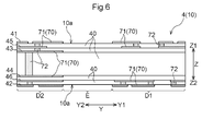
- the substrate main body 10 includes an even-numbered multi-layer structure 4 including a first layer 41 and a second layer 42.
- the multilayer structure 4 further includes a third layer 43 and a fourth layer 44. That is, the substrate main body 10 is an even-numbered multilayer substrate (multilayer printed circuit board).
- the "even number layer” means that the number of wiring layers (conductor layers) to be laminated is an even number. That is, the even-numbered multi-layer structure 4 has an even-numbered layer wiring structure.
- the wiring layer is a layer on which a wiring pattern 71 using a conductor foil 70 (copper foil or the like) is formed, and an even number of wiring layers included in the multilayer structure 4 are formed in the thickness direction Z via the insulating layer 40. It is laminated.
- Each of the first layer 41, the second layer 42, the third layer 43, and the fourth layer 44 is a wiring layer.
- the substrate main body 10 includes a 6-layer multi-layer structure 4, and the multi-layer structure 4 further includes a 5th layer 45 and a 6th layer 46.
- Each of the fifth layer 45 and the sixth layer 46 is a wiring layer.
- the insulating layer 40 is formed using, for example, a prepreg.
- the first layer 41 is formed on the surface layer portion 10a of the first side Z1 in the substrate main body portion 10, and the second layer 42 is formed on the surface layer portion 10a of the second side Z2 in the substrate main body portion 10. It is formed.
- the third layer 43 and the fourth layer 44 are the two layers closest to the central portion in the thickness direction Z of the substrate main body portion 10.
- the third layer 43 is arranged between the first layer 41 and the fourth layer 44.
- the fifth layer 45 is arranged between the first layer 41 and the third layer 43
- the sixth layer 46 is arranged between the second layer 42 and the fourth layer 44.
- first layer 41, the fifth layer 45, the third layer 43, the fourth layer 44, the sixth layer 46, and the second layer 42 are laminated in the order described from the first side Z1.
- first side Z1 corresponds to "one side in the thickness direction”
- second side Z2 corresponds to "the other side in the thickness direction”.
- the multilayer structure 4 is formed with vias 72 (for example, filled vias) for electrically connecting different wiring layers (for example, wiring layers adjacent to each other in the thickness direction Z).
- the via 72 is formed so as to penetrate the insulating layer 40, and a conductor (copper or the like) is provided inside the via 72.
- Such a multilayer structure 4 is formed by using, for example, a build-up method.
- a resist permanent resist, solder resist
- an opening is provided in the resist so as to expose the first layer 41.
- a pad for mounting components such as the drive circuit 2 and the transformer 8 on the first layer 41 is formed.
- a resist is laminated on the second side Z2 with respect to the second layer 42, and the component is mounted on the second layer 42 by forming an opening in the resist so as to expose the second layer 42. Pads for this are formed.
- a low voltage region A in which the low voltage circuit 53 is arranged and a high voltage region B in which the high voltage circuit 50 is arranged are provided on both the first layer 41 and the second layer 42.
- An insulating region E that electrically insulates the low voltage region A and the high voltage region B is formed.
- the low voltage region A formed in the first layer 41 is referred to as the first layer low voltage region A1
- the low voltage region A formed in the second layer 42 is referred to as the second layer low voltage region A2
- the first layer The high voltage region B formed in the 41
- the high voltage region B formed in the second layer 42 is referred to as the second layer high voltage region B2.
- the low voltage region A includes a circuit region having the second ground G2 as a reference potential
- the high voltage region B includes a circuit region having the first ground G1 as a reference potential.
- the first drive circuit 21, the second drive circuit 22, the first transformer 81, and the second transformer 82 are arranged so as to connect the low voltage region A and the high voltage region B across the insulation region E.
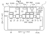
- FIG. 3 is a plan view of the substrate main body 10 viewed from the first side Z1
- FIG. 4 is a perspective plan view of the substrate main body 10 seen from the first side Z1.
- a part of the parts that is, the parts mounted on the first layer 41
- the board main body 10 specifically, the first drive circuit 21, the first The transformer 81, the second transformer 82, and the first connection portion 51a
- the low voltage arranged in the first layer low voltage region A1, the first layer high voltage region B1, and the first layer low voltage region A1 is shown.
- the circuit 53 and the high voltage circuit 50 arranged in the first layer high voltage region B1 are shown schematically in a simplified manner. Further, in FIG.
- a part (specifically, the second drive circuit 22) of the parts (that is, the parts mounted on the second layer 42) arranged on the second side Z2 with respect to the board main body portion 10
- 53 and the high voltage circuit 50 arranged in the second layer high voltage region B2 are shown schematically in a simplified manner.
- Each of the first high-voltage circuit 51 and the second high-voltage circuit 52 is provided with a transformer 8 arranged so as to straddle the insulation region E and transmit electric power between the low-voltage region A and the high-voltage region B.
- the first high-voltage circuit 51 includes a first transformer 81 that is arranged so as to straddle the insulation region E and transmits power between the low-voltage region A and the high-voltage region B, and has a second high voltage.
- the voltage circuit 52 includes a second transformer 82 that is arranged so as to straddle the insulation region E and transmits power between the low voltage region A and the high voltage region B.
- each of the first transformer 81 and the second transformer 82 is arranged so as to straddle the insulation region E, and transmits electric power between the low voltage region A and the high voltage region B.
- all the transformers 8 are the substrate main bodies. It is arranged on the same side in the thickness direction Z with respect to the portion 10 (specifically, the first side Z1 with respect to the substrate main body portion 10). That is, all the transformers 8 are arranged so as to connect the first layer low voltage region A1 and the first layer high voltage region B1 across the insulation region E.
- all the first transformers 81 and the second transformers 82 are arranged on the first side Z1 with respect to the substrate main body 10. Therefore, at least the second high voltage circuit 52 of the first high voltage circuit 51 and the second high voltage circuit 52 needs to be arranged separately in the first layer high voltage region B1 and the second layer high voltage region B2. However, when only the second high voltage circuit 52 is arranged separately in the first layer high voltage region B1 and the second layer high voltage region B2, the first side Z1 and the second side Z2 are arranged with respect to the substrate main body 10. The total area of the high voltage region B tends to be biased between the two.
- the first high voltage circuit 51 is also divided into a first layer high voltage region B1 and a second layer high voltage region B2. Since they are arranged, even when all the first transformers 81 and the second transformers 82 are arranged on the first side Z1 with respect to the substrate main body 10 as described above, the substrate main body 10 is arranged. It is easy to prevent a large bias in the total area of the high voltage region B between the first side Z1 and the second side Z2. As a result, it is easy to reduce the size of the control board 1 in a plan view.
- Each of the first high voltage circuit 51 and the second high voltage circuit 52 is arranged so as to straddle the insulation region E and transmits a signal (switching control signal SW or the like) between the low voltage region A and the high voltage region B.
- the drive circuit 2 for transmission is provided.
- the first high voltage circuit 51 is arranged so as to straddle the insulation region E, and transmits a signal (first switching control signal SW1 or the like) between the low voltage region A and the high voltage region B.
- the first drive circuit 21 is provided, and the second high voltage circuit 52 is arranged so as to straddle the insulation region E and transmits a signal (second switching control signal SW2 or the like) between the low voltage region A and the high voltage region B.
- the second drive circuit 22 is provided.
- the drive circuits 2 are arranged on both sides of the substrate main body 10 in the thickness direction Z.
- all the first drive circuits 21 (here, three first drive circuits 21) are arranged on the first side Z1 with respect to the substrate main body 10, and all the second drive circuits 22 (here, here).
- the three second drive circuits 22) are arranged on the second side Z2 with respect to the substrate main body 10. That is, all the first drive circuits 21 are arranged so as to connect the first layer low voltage region A1 and the first layer high voltage region B1 across the insulation region E, and all the second drive circuits 22 are arranged. It is arranged so as to connect the second layer low voltage region A2 and the second layer high voltage region B2 across the insulation region E.
- the low voltage circuit 53 arranged in the low voltage region A includes a control circuit 6, a signal transmission circuit for transmitting a switching control signal SW from the control circuit 6 to the drive circuit 2, and a power supply circuit 7.
- a power supply control circuit 90 and a power transmission circuit for transmitting a primary side voltage from the power supply control circuit 90 to the transformer 8 (specifically, the primary winding L1) are included.
- the low voltage circuit 53 is divided into a first layer low voltage region A1 and a second layer low voltage region A2.
- the circuit is divided into at least a portion arranged in the first region and a portion arranged in the second region. This means that the circuit may include a portion arranged in yet another region.
- the portion of the low voltage circuit 53 arranged in the first layer low voltage region A1 is formed by using the wiring pattern 71 provided in the first layer 41, and is arranged in the second layer low voltage region A2 of the low voltage circuit 53.
- the portion to be formed is formed by using the wiring pattern 71 provided on the second layer 42.
- the first high voltage circuit 51 arranged in the high voltage region B includes a signal transmission circuit that transmits the first switching control signal SW1 from the first drive circuit 21 to the first connection portion 51a, and a first.
- a power transmission circuit for transmitting a secondary side voltage from a transformer 81 (specifically, a secondary winding L2) to a first drive circuit 21 is included.
- the first connection portion 51a is a connection portion with the first switching element 31 in the first high voltage circuit 51.
- the first switching control signal SW1 is transmitted from the first drive circuit 21 to the first switching element 31 via the first connection portion 51a.
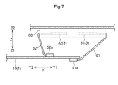
- the first connection portion 51a is provided in the first layer high voltage region B1. As shown in FIG.
- the first connection portion 51a includes a connector to which the first flexible substrate 61 having flexibility is connected. Then, the first high voltage circuit 51 is connected to the first switching element 31 via the first flexible substrate 61.
- the first connection portion 51a is provided with a hole portion that penetrates the substrate main body portion 10 in the thickness direction Z instead of the connector, and the connection terminal of the first switching element 31 is arranged so as to penetrate the hole portion. It is also possible to have a configuration in which the first connection portion 51a is connected in the state of being connected.
- the first high voltage circuit 51 arranged in the high voltage region B further represents the detection result of the detection circuit (current detection circuit, temperature detection circuit, etc.) provided in the first switching element 31.
- a signal transmission circuit that transmits a signal from the first connection portion 51a to the signal transmission element 23 is also included.
- the signal transmission element 23 includes an insulating element (insulating element for signal transmission) such as a photocoupler or a magnetic coupler.
- the signal transmission element 23 is arranged so as to connect the low voltage region A and the high voltage region B across the insulation region E.
- the signal representing the detection result is transmitted from the high voltage region B to the low voltage region A via the signal transmission element 23, and is input to the control circuit 6.
- all the signal transmission elements 23 are arranged on the second side Z2 with respect to the substrate main body 10. That is, all the signal transmission elements 23 are arranged so as to connect the second layer low voltage region A2 and the second layer high voltage region B2 across the insulation region E.
- At least a part of the first high voltage circuit 51 is arranged in the first layer high voltage region B1.
- the portion of the first high voltage circuit 51 arranged in the first layer high voltage region B1 is formed by using the wiring pattern 71 provided in the first layer 41.
- the first high voltage circuit 51 is divided into a first layer high voltage region B1 and a second layer high voltage region B2.
- the portion of the first high voltage circuit 51 arranged in the second layer high voltage region B2 is formed by using the wiring pattern 71 provided in the second layer 42.
- the portion arranged in the first layer high voltage region B1 and the portion arranged in the second layer high voltage region B2 in one first high voltage circuit 51 are arranged so as to have overlapping portions in a plan view. There is. Then, the portion of the first high voltage circuit 51 arranged in the first layer high voltage region B1 and the portion arranged in the second layer high voltage region B2 are electrically connected via the via 72. There is.
- the second high voltage circuit 52 arranged in the high voltage region B includes a signal transmission circuit that transmits the second switching control signal SW2 from the second drive circuit 22 to the second connection portion 52a, and a second.
- a power transmission circuit for transmitting a secondary side voltage from a transformer 82 (specifically, a secondary winding L2) to a second drive circuit 22 is included.
- the second connection portion 52a is a connection portion with the second switching element 32 in the second high voltage circuit 52.
- the second switching control signal SW2 is transmitted from the second drive circuit 22 to the second switching element 32 via the second connection portion 52a.
- the second connection portion 52a is provided in the second layer high voltage region B2. As shown in FIG.
- the second connection portion 52a includes a connector to which the second flexible substrate 62 having flexibility is connected. Then, the second high voltage circuit 52 is connected to the second switching element 32 via the second flexible substrate 62.
- the second connection portion 52a is provided with a hole portion that penetrates the substrate main body portion 10 in the thickness direction Z instead of the connector, and the connection terminal of the second switching element 32 is arranged so as to penetrate the hole portion. It is also possible to have a configuration in which the second connection portion 52a is connected to the second connection portion 52a in the state of being connected.
- At least a part of the second high voltage circuit 52 is arranged in the second layer high voltage region B2.
- the portion of the second high voltage circuit 52 arranged in the second layer high voltage region B2 is formed by using the wiring pattern 71 provided in the second layer 42.
- the second high voltage circuit 52 is divided into a first layer high voltage region B1 and a second layer high voltage region B2.
- the portion of the second high voltage circuit 52 arranged in the first layer high voltage region B1 is formed by using the wiring pattern 71 provided in the first layer 41.
- the portion arranged in the first layer high voltage region B1 and the portion arranged in the second layer high voltage region B2 in one second high voltage circuit 52 are arranged so as to have overlapping portions in a plan view. There is. Then, the portion arranged in the first layer high voltage region B1 and the portion arranged in the second layer high voltage region B2 in one second high voltage circuit 52 are electrically connected via the via 72. There is.
- the drive circuit 2 As the element in which the drive circuit 2 is formed, an element in which the drive circuit 2 and the insulating element are built in one package is used, but the drive circuit 2 and the insulating element are used. It is also possible to have a configuration in which and is a separate component.
- the insulating element is arranged so as to connect the low voltage region A and the high voltage region B across the insulating region E, and the drive circuit 2 is arranged in the high voltage region B. That is, in this case, the high voltage circuit 50 arranged in the high voltage region B also includes the drive circuit 2.
- the first high-voltage circuit 51 arranged in the high-voltage region B includes the first drive circuit 21, and the second high-voltage circuit 52 arranged in the high-voltage region B includes the second drive circuit 22. included.
- the inverter 100 includes three arms 33, a U-phase arm 33U, a V-phase arm 33V, and a W-phase arm 33W. That is, the inverter 100 includes three first switching elements 31 and three second switching elements 32. Therefore, in the high-voltage region B, the U-phase first high-voltage region BU1 in which the first high-voltage circuit 51 (U-phase first high-voltage circuit 51) connected to the U-phase first switching element 31 is arranged. The U-phase second high-voltage region BU2 in which the second high-voltage circuit 52 (U-phase second high-voltage circuit 52) connected to the U-phase second switching element 32 is arranged, and the V-phase first.
- V-phase first high-voltage region BV1 in which the first high-voltage circuit 51 (V-phase first high-voltage circuit 51) connected to the switching element 31 is arranged, and to the V-phase second switching element 32.
- the V-phase second high-voltage region BV2 in which the second high-voltage circuit 52 (V-phase second high-voltage circuit 52) is arranged, and the first high-voltage circuit 51 (1st high-voltage circuit 51) connected to the W-phase first switching element 31.
- a W-phase second high-voltage region BW2 in which the circuit 52) is arranged is included.
- the first high voltage circuit 51 and the second high voltage circuit 52 are respectively arranged separately in the first layer high voltage region B1 and the second layer high voltage region B2. Therefore, the U-phase first high-voltage region BU1, the U-phase second high-voltage region BU2, the V-phase first high-voltage region BV1, the V-phase second high-voltage region BV2, the W-phase first high-voltage region BW1, and W.
- Each of the phase second high voltage regions BW2 includes a portion formed in the first layer 41 and a portion formed in the second layer 42. That is, as shown in FIG.
- the first layer high voltage region B1 includes a part of the U-phase first high-voltage region BU1, a part of the U-phase second high-voltage region BU2, and a V-phase first high-voltage region.
- a part of BV1, a part of V-phase second high-voltage region BV2, a part of W-phase first high-voltage region BW1, and a part of W-phase second high-voltage region BW2 are included.
- the second layer high voltage region B2 includes another part of the U-phase first high-voltage region BU1, another part of the U-phase second high-voltage region BU2, and the V-phase first. 1
- the high voltage region B is arranged on the fifth side Y1 with respect to the low voltage region A.
- the first layer high voltage region B1 is arranged on the fifth side Y1 with respect to the first layer low voltage region A1
- the second layer high voltage region B2 is relative to the second layer low voltage region A2. Is arranged on the fifth side Y1.
- the insulating region E that electrically insulates the low voltage region A and the high voltage region B is formed so as to extend between the low voltage region A and the high voltage region B along the first direction X. ..
- the portion on the insulation region E side in the first layer high voltage region B1 (here, the portion on the sixth side Y2) and the portion on the insulation region E side in the second layer high voltage region B2 (here, the third).
- the U-phase second high-voltage region BU2 In the portion of Y2 on the 6 side), the U-phase second high-voltage region BU2, the U-phase first high-voltage region BU1, the V-phase first high-voltage region BV1, the V-phase second high-voltage region BV2, and the W-phase second high-voltage region.
- the region BW2 and the W-phase first high-voltage region BW1 are arranged in the order described from the fourth side X2.
- the first layer high voltage region B1 and the second layer high voltage region B2 are arranged so as to have overlapping portions in a plan view along the thickness direction Z. ..
- the first layer high voltage region B1 (specifically, the U phase first high voltage region BU1, the U phase second high voltage region BU2, the V phase first high voltage region BV1, the V phase second).
- the portion included in the first layer high voltage region B1 in each of the high voltage region BV2, the W phase first high voltage region BW1, and the W phase second high voltage region BW2) is indicated by hatching, and the second layer high voltage is shown.
- Region B2 (Specifically, U-phase first high-voltage region BU1, U-phase second high-voltage region BU2, V-phase first high-voltage region BV1, V-phase second high-voltage region BV2, W-phase first high-voltage
- the portion included in the second layer high voltage region B2 in each of the region BW1 and the W phase second high voltage region BW2) is shown surrounded by a solid line frame.
- the first layer low voltage region A1 and the second layer low voltage region A2 are arranged so as to have overlapping portions in a plan view. In FIG. 5, the first layer low voltage region A1 is shown by hatching, and the second layer low voltage region A2 is shown surrounded by a solid line frame.
- the first layer high voltage region B1 and the second layer low voltage region A2 are arranged so as not to overlap in a plan view, and the second layer high voltage region B2 and the first layer low voltage region A1 are , Are arranged so that they do not overlap in a plan view.
- first layer high voltage region B1 and the second layer high voltage region B2 are arranged so as to have overlapping portions in a plan view in this way, the first layer high voltage region B1 and the second layer high voltage region B2 Ensuring electrical insulation between the two can be a problem.
- first overlapping region A region in which the other portion of the voltage circuit 52 overlaps in a plan view
- second overlapping region a portion in the first layer high voltage region B1 where the second high voltage circuit 52 is arranged.
- second overlapping region in the region where the portion of the second layer high voltage region B2 where another second high voltage circuit 52 is arranged overlaps in a plan view.
- the first overlapping region at least a portion formed in the first layer 41 in the U-phase first high-voltage region BU1 and a second layer 42 in the U-phase second high-voltage region BU2 are formed.
- a region in which the above portions overlap in a plan view a portion formed in the first layer 41 in the V-phase first high-voltage region BV1 and a portion formed in the second layer 42 in the V-phase second high-voltage region BV2.
- the second overlapping region at least the portion formed in the first layer 41 in the V-phase second high-voltage region BV2 and the second layer 42 in the W-phase second high-voltage region BW2. There is a region that overlaps with the formed portion in a plan view.
- This control board 1 avoids the problem of electrical insulation by adopting the configuration described below.
- the region of the substrate main body 10 that overlaps both the first layer high voltage region B1 and the second layer high voltage region B2 in a plan view is referred to as a high voltage overlapping region D1 (see FIG. 6).
- the region of the substrate main body 10 that overlaps both the first layer low voltage region A1 and the second layer low voltage region A2 in a plan view is referred to as a low voltage overlapping region D2 (see FIG. 6).
- wiring patterns 71 are provided in each of the first layer 41, the second layer 42, the third layer 43, and the fourth layer 44.
- wiring patterns 71 are provided in each of the first layer 41, the second layer 42, the third layer 43, the fourth layer 44, the fifth layer 45, and the sixth layer 46. ing. That is, in the low-voltage overlapping region D2, the wiring pattern 71 is provided in all the layers (wiring layers) included in the multilayer structure 4.
- the wiring pattern 71 is provided in the first layer 41 and the second layer 42, and the wiring pattern 71 is provided in the third layer 43 and the fourth layer 44 closest to the central portion in the thickness direction Z. Not provided.
- the wiring pattern 71 is provided in the first layer 41, the second layer 42, the fifth layer 45, and the sixth layer 46 in the high-voltage overlapping region D1.
- the thickness (width in the thickness direction Z) of the insulating layer 40 (for example, the core insulating layer) arranged between the third layer 43 and the fourth layer 44 is the same as that of the other insulating layer 40. It is formed to be larger than the thickness, which also facilitates ensuring the electrical insulation between the first layer high voltage region B1 and the second layer high voltage region B2. Further, by providing a layer without the wiring pattern 71 in the high-voltage overlapping region D1, the coupling capacitance between the first layer high voltage region B1 and the second layer high voltage region B2 is suppressed to a small value, and noise due to capacitive coupling is reduced. It's getting easier.
- each wiring pattern 71 is formed so that the wiring patterns 71 are orthogonal to each other in a plan view at a portion where the wiring patterns 71 provided in the adjacent wiring layers overlap each other in a plan view. ing. This makes it possible to keep the coupling capacitance between adjacent wiring layers small. Since the wiring pattern 71 is not provided in the third layer 43 and the fourth layer 44 in the high-voltage overlapping region D1, the wiring layers adjacent to the fifth layer 45 in the high-voltage overlapping region D1 are the first layer 41 and the first layer 41. The 6th layer 46, and the wiring layers adjacent to the 6th layer 46 are the 2nd layer 42 and the 5th layer 45.
- the wiring pattern 71 is formed in the third layer 43 and the fourth layer 44 in the region. It can be configured not to be provided. In particular, a region in which only one of the first layer high voltage region B1 and the second layer high voltage region B2 overlaps in the plan view is a region in which both the high voltage region B and the low voltage region A overlap in the plan view. In some cases, from the viewpoint of ensuring electrical insulation, it is preferable that the third layer 43 and the fourth layer 44 are not provided with the wiring pattern 71.
- the region of the substrate main body 10 that overlaps only one of the first layer high voltage region B1 and the second layer high voltage region B2 in a plan view is defined as the target region D3 (see FIG. 5).
- the target region D3 there is a region that overlaps only the first layer high voltage region B1 in a plan view and a region that overlaps only the second layer high voltage region B2 in a plan view.
- wiring for connecting the portion arranged in the first layer high voltage region B1 and the portion arranged in the second layer high voltage region B2 in the high voltage circuit 50 is not shown.
- the pattern 71 is an intermediate layer which is a layer between the first layer 41 and the second layer 42 in the target region D3 (in the present embodiment, the third layer 43, the fourth layer 44, the fifth layer 45, and the sixth layer). It is provided in at least one of the layers 46).
- each of the first high voltage circuit 51 and the second high voltage circuit 52 is separately arranged in the first layer high voltage region B1 and the second layer high voltage region B2. Therefore, the wiring pattern 71 for connecting the portion arranged in the first layer high voltage region B1 and the portion arranged in the second layer high voltage region B2 in the first high voltage circuit 51 is intermediate in the target region D3.
- a wiring pattern 71 provided on the layer and for connecting a portion of the second high voltage circuit 52 arranged in the first layer high voltage region B1 and a portion arranged in the second layer high voltage region B2 is provided. , It is provided in the intermediate layer in the target region D3.
- the fifth layer 45 and the sixth layer 46 are provided with a wiring pattern 71 (power supply pattern) connected to the power supply and a wiring pattern 71 (ground pattern) connected to the ground. Therefore, in the high-voltage overlapping region D1, the wiring pattern 71 (signal pattern) for transmitting a signal is mainly provided in the first layer 41 and the second layer 42. In the present embodiment, the signal pattern is also provided in the fifth layer 45 and the sixth layer 46.
- the power supply pattern is connected to, for example, the wiring pattern 71 connected to the positive electrode side of the second DC power supply 12 or the positive electrode side of the power supply (upper stage drive voltage VH or lower stage drive voltage VL) generated by the power supply circuit 7.
- the wiring pattern 71 is set.
- the ground pattern is, for example, a wiring pattern 71 connected to the first ground G1 or a wiring pattern 71 connected to the second ground G2.
- the power supply pattern which is the wiring pattern 71 connected to the power supply
- the ground pattern which is the wiring pattern 71 connected to the ground
- the power supply pattern and the ground pattern may be thicker or wider than the signal pattern, which is the wiring pattern 71 for transmitting signals. There are many. Therefore, the power supply pattern and the ground pattern generally have higher noise immunity and shielding action than the signal pattern.
- a power supply pattern or a ground pattern having such properties is arranged between the first layer 41 and the second layer 42 (specifically, in the fifth layer 45 and the sixth layer 46). Therefore, it is easy to suppress noise propagation between the first layer high voltage region B1 and the second layer high voltage region B2 in the high voltage overlapping region D1.
- the first connection is defined as the high voltage region B in which the first connection portion 51a is arranged as the first connection region C1 and the high voltage region B in which the second connection portion 52a is arranged as the second connection region C2.
- the region C1 includes at least a part in the first layer high voltage region B1
- the second connection region C2 includes at least a part in the second layer high voltage region B2.
- the first connection portion 51a is a connector mounted on the first layer 41
- the second connection portion 52a is a connector mounted on the second layer 42. Therefore, in the present embodiment, the entire first connection region C1 is included in the first layer high voltage region B1, and the entire second connection region C2 is included in the second layer high voltage region B2.
- the first connection region C1 and the second connection region C2 connected to the first switching element 31 and the second switching element 32 constituting one arm 33 have overlapping portions in a plan view. It is arranged like this.
- the first connection portion 51a and the second connection portion 51a connected to the first switching element 31 and the second switching element 32 constituting one arm 33 are formed.
- the pair with the connection portion 52a can be arranged on the control board 1 so as to be arranged in the same order as the arrangement order of the first switching element 31 and the second switching element 32 in the inverter 100. Therefore, the connection between the control board 1 and the inverter 100 becomes easy.
- first connection region C1 connected to the U-phase first switching element 31 and the second connection region C2 connected to the U-phase second switching element 32 overlap in a plan view.
- first connection region C1 connected to the U-phase first switching element 31 corresponds to the portion formed in the first layer 41 in the U-phase first high-voltage region BU1 (see FIG. 3)
- the U connection region C2 connected to the second phase switching element 32 corresponds to a portion formed in the second layer 42 in the U-phase second high voltage region BU2 (see FIG. 4).
- first connection region C1 connected to the first switching element 31 of the V phase and the second connection region C2 connected to the second switching element 32 of the V phase have overlapping portions in a plan view. Is located in.
- first connection region C1 connected to the V-phase first switching element 31 corresponds to a portion formed in the first layer 41 in the V-phase first high-voltage region BV1 (see FIG. 3), and is V.
- the second connection region C2 connected to the second switching element 32 of the phase corresponds to a portion formed in the second layer 42 in the V-phase second high voltage region BV2 (see FIG. 4).
- first connection region C1 connected to the W-phase first switching element 31 and the second connection region C2 connected to the W-phase second switching element 32 have overlapping portions in a plan view. Is located in.
- first connection region C1 connected to the W-phase first switching element 31 corresponds to a portion formed in the first layer 41 in the W-phase first high-voltage region BW1 (see FIG. 3), and is W.
- the second connection region C2 connected to the second phase switching element 32 corresponds to a portion formed in the second layer 42 in the W phase second high voltage region BW2 (see FIG. 4).
- the second connection portion 52a connected to the U-phase second switching element 32 and the first connection portion 51a connected to the U-phase first switching element 31 ,
- the second connecting portion 52a connected to the second switching element 32 of the V phase, the first connecting portion 51a connected to the first switching element 31 of the V phase, and the second connecting portion 32 connected to the second switching element 32 of the W phase.
- the two connection portions 52a and the first connection portion 51a connected to the W-phase first switching element 31 are arranged in the order described from the fourth side X2.
- the layers in which the wiring pattern 71 is not provided in the high-voltage overlapping region D1 are only the third layer 43 and the fourth layer 44 closest to the central portion in the thickness direction Z. explained.
- the present disclosure is not limited to such a configuration, and in the high-voltage overlapping region D1, in addition to the third layer 43 and the fourth layer 44, the layers adjacent to the third layer 43 and the fourth layer 44 (provided that the third layer 43 and the fourth layer 44 are adjacent to the third layer 43 and the fourth layer 44
- the wiring pattern 71 may not be provided in the first layer 41 and the second layer 42).
- the wiring pattern 71 is not provided in the third layer 43, the fourth layer 44, the fifth layer 45, and the sixth layer 46 in the high-voltage overlapping region D1. Can be done.
- the substrate main body 10 includes the six-layer multilayer structure 4 has been described as an example.
- the present disclosure is not limited to such a configuration, and the number of layers of the multilayer structure 4 can be appropriately changed.
- the substrate main body 10 has a configuration including a multi-layer structure 4 having four layers (that is, a configuration without the fifth layer 45 and the sixth layer 46), or the substrate main body 10 has an even-numbered layer of eight or more layers.
- first connection region C1 and the second connection region C2 connected to the first switching element 31 and the second switching element 32 constituting one arm 33 overlap in a plan view.
- the configuration in which the devices are arranged so as to have the above is described as an example.
- the present disclosure is not limited to such a configuration, for example, a first connection region C1 connected to a first switching element 31 constituting one arm 33 and a second switching element constituting another arm 33.
- the second connection region C2 connected to 32 may be arranged so as to have overlapping portions in a plan view.
- a configuration in which all the transformers 8 (six transformers 8 in the above embodiment) are arranged on the first side Z1 with respect to the substrate main body 10 will be described as an example.
- the present disclosure is not limited to such a configuration, and all transformers 8 may be arranged on the second side Z2 with respect to the substrate main body 10.
- the transformer 8 is divided into a first side Z1 and a second side Z2 with respect to the substrate main body 10.
- the transformer 8 may be arranged.
- all the first transformers 81 are arranged on the first side Z1 with respect to the substrate main body 10
- all the second transformers 82 are arranged on the second side Z2 with respect to the substrate main body 10. Can be done.
- the first high voltage circuit 51 and the second high voltage circuit 52 are respectively arranged separately in the first layer high voltage region B1 and the second layer high voltage region B2.
- both the first high voltage circuit 51 and the second high voltage circuit 52 correspond to the "target high voltage circuit".
- the present disclosure is not limited to such a configuration, and only one of the first high voltage circuit 51 and the second high voltage circuit 52 is divided into the first layer high voltage region B1 and the second layer high voltage region B2. It can also be configured to be arranged separately.
- only the second high voltage circuit 52 may be arranged separately in the first layer high voltage region B1 and the second layer high voltage region B2.
- the second high voltage circuit 52 corresponds to the "target high voltage circuit".
- the transformer 8 is divided into the first side Z1 and the second side Z2 with respect to the substrate main body 10 (specifically, the first transformer 81 is the first side with respect to the substrate main body 10).
- the second transformer 82 is arranged on the second side Z2 with respect to the substrate main body 10, and both the first high-voltage circuit 51 and the second high-voltage circuit 52 are first. It is also possible to configure the layer high voltage region B1 and the second layer high voltage region B2 so that they are not separately arranged.
- the first layer high voltage region B1 and the second layer high voltage region B2 are arranged so as to have overlapping portions in a plan view, and the first layer low voltage region A1 and the second layer are arranged.
- An example of a configuration in which the low voltage region A2 is arranged so as to have an overlapping portion in a plan view has been described.
- the present disclosure is not limited to such a configuration, and the first layer high voltage region B1 and the second layer high voltage region B2 are arranged so as not to have an overlapping portion in a plan view.
- the layer low voltage region A1 and the second layer low voltage region A2 may be arranged so as not to have overlapping portions in a plan view, or a combination thereof may be used.
- the plate-shaped substrate main body portion (10) on which the (5) is formed is provided, and the drive control circuit (5) has a higher operating voltage than the low voltage circuit (53) and the low voltage circuit (53).
- the first transformer (81) that supplies the drive voltage of the second high voltage circuit (52) to be connected and the first switching element (31) from the low voltage circuit (53) to the first high voltage circuit (51).
- Reference numerals (10) are the first layer (41) formed on the surface layer portion (10a) on one side (Z1) of the substrate main body portion (10) in the thickness direction (Z), and the thickness direction (Z).
- the first layer (41) and the second layer are provided with an even-layered multi-layer structure (4) including a second layer (42) formed on the surface layer portion (10a) on the other side (Z2) of the above.
- the first high voltage circuit (51) and at least a part of the second high voltage circuit (52) are formed on the surface layer portion (10a) on the substrate main body portion (10) opposite to each other. Since it can be arranged separately in the first layer high voltage region (B1) and the second layer high voltage region (B2) formed in the first high voltage circuit (51), the components and wiring constituting the first high voltage circuit (51) and the first layer. 2. It becomes easy to arrange the parts and wirings constituting the high-voltage circuit (52) so as to be close to each other in a plan view or to overlap in a plan view. As a result, it is possible to secure a high degree of freedom in arranging parts and wiring, and to reduce the size of the control board (1) in a plan view.
- the first layer high voltage region (B1) and the second layer high voltage region (B2) are arranged so as to have overlapping portions in a plan view along the thickness direction (Z). Is suitable.
- the multilayer structure (4) Including the third layer (43) and the fourth layer (44), which are the two layers closest to the central portion in the thickness direction (Z), and the low layer formed in the first layer (41).
- the first layer low voltage region (A1) which is a voltage region (A) and the second layer low voltage region (A2) which is the low voltage region (A) formed in the second layer (42) are Arranged so as to have overlapping portions in the plan view, the first layer high voltage region (B1) and the second layer high voltage region (B2) in the plan view of the substrate main body (10).
- the region overlapping both of the above is defined as the high voltage overlapping region (D1)
- the region overlapping both of the first layer low voltage region (A1) and the second layer low voltage region (A2) is defined as the low voltage overlapping region (D2).
- the conductor foil (70) is applied to each of the first layer (41), the second layer (42), the third layer (43), and the fourth layer (44).
- the wiring pattern (71) is provided in the first layer (41) and the second layer (42), and the first layer (41) is provided. It is preferable that the wiring pattern (71) is not provided in the third layer (43) and the fourth layer (44).
- the first layer high voltage region (B1) and the second layer high voltage region (B2) are high voltage regions (B) in which a high voltage circuit (50) having a higher operating voltage than the low voltage circuit (53) is arranged. Therefore, when the first layer high voltage region (B1) and the second layer high voltage region (B2) are arranged so as to have overlapping portions in a plan view as described above, the first layer high voltage region It is usually difficult to ensure the electrical insulation between (B1) and the second layer high voltage region (B2).
- the wiring pattern (71) is provided in each of the first layer (41), the second layer (42), the third layer (43), and the fourth layer (44), whereas the substrate main body portion.
- the first layer (41) and the second layer The wiring pattern (71) is provided in (42), and the wiring pattern (71) is not provided in the third layer (43) and the fourth layer (44) closest to the central portion in the thickness direction (Z). .. Therefore, in the low-voltage overlapping region (D2), control is performed by forming a circuit using all of the first layer (41), the second layer (42), the third layer (43), and the fourth layer (44).
- the first layer high voltage region (B1) and the second layer high voltage are provided. It is easy to properly secure the electrical insulation between the region (B2) and the region (B2). Further, the coupling capacitance between the first layer high voltage region (B1) and the second layer high voltage region (B2) is suppressed to be small, and noise due to capacitive coupling can be easily reduced. Therefore, it is possible to arrange the first layer high voltage region (B1) and the second layer high voltage region (B2) so as to have overlapping portions in a plan view while avoiding problems of electrical insulation and noise. It is possible.
- first transformer (81) and the second transformer (82) are arranged so as to straddle the insulating region (E), and the low voltage region (A) and the high voltage region (B) are arranged. All the first transformers (81) and the second transformers (82) are arranged on the same side in the thickness direction (Z) with respect to the substrate main body (10). It is preferable that it is.
- the first transformer (81) and the second transformer (82), which are generally heavier than other parts, are all in the thickness direction (10) with respect to the substrate main body (10). It can be placed on the same side of Z). Therefore, in the process of mounting the first transformer (81) and the second transformer (82) on the board main body (10), all the first transformers (81) and the second transformer (82) are on the board main body (10). It can be performed in a state of being supported from below. Therefore, the first transformer (81) and the second transformer (82) are separately arranged on both sides in the thickness direction (Z) with respect to the substrate main body (10), as compared with the case where the first transformer (81) and the second transformer (82) are separately arranged on both sides in the thickness direction (Z). ) And the second transformer (82) on the substrate main body (10) can be simplified.
- the target high-voltage circuit which is at least one of the first high-voltage circuit (51) and the second high-voltage circuit (52), is the first-layer high-voltage region (B1) and the second-layer high-voltage region.
- the first layer high voltage region (B1) and the second layer high voltage region are arranged separately from (B2), and in a plan view along the thickness direction (Z) in the substrate main body (10).
- the region overlapping only one of (B2) is set as the target region (D3), and the portion arranged in the first layer high voltage region (B1) and the second layer high voltage region in the target high voltage circuit.
- the wiring pattern (71) using the conductor foil (70) for connecting to the portion arranged in (B2) is the first layer in the multilayer structure (4) in the target region (D3). It is preferable that the layer is provided between the second layer (42) and the second layer (42).
- the first high voltage circuit It is necessary to separately arrange the target high voltage circuit, which is at least one of the 51) and the second high voltage circuit (52), in the first layer high voltage region (B1) and the second layer high voltage region (B2). .. According to this configuration, the portion arranged in the first layer high voltage region (B1) and the portion arranged in the second layer high voltage region (B2) in the target high voltage circuit are placed in the target region (D3). It can be appropriately connected by the wiring pattern (71) provided in the layer between the first layer (41) and the second layer (42).
- control board according to the present disclosure should be able to exert at least one of the above-mentioned effects.
Abstract
In the present invention, a substrate part (10) comprises a multilayer structure (4) having an even number of layers, including: a first layer (41) formed in a front layer part (10a) on one side (Z1); and a second layer (42) formed in a front layer part (10a) on another side (Z2). The first layer (41) and the second layer (42) each have formed therein: a low-voltage region where a low-voltage circuit is arranged; a high-voltage region where a high-voltage circuit is arranged; and an insulation region (E) that electrically insulates the low-voltage region and the high-voltage region from each other. At least a portion of a first high-voltage circuit is arranged in a first layer high-voltage region formed in the first layer (41), and at least a portion of a second high voltage circuit is arranged in a second layer high-voltage region formed in the second layer (42).
Description
本発明は、インバータを制御対象とする制御基板に関する。
The present invention relates to a control board for controlling an inverter.
インバータを制御対象とする制御基板の一例が、国際公開第2016/88211号(特許文献1)に開示されている。以下、背景技術の説明において括弧内に示す符号は特許文献1のものである。特許文献1の制御基板としての基板(11)には、制御回路(CNT)と、制御回路(CNT)からの制御信号を受けてスイッチング素子(Q1~Q6)を駆動する駆動回路(DR1~DR6)と、駆動回路(DR1~DR2)に給電する電源回路(P1~P6)と、が設けられている。基板(11)上には、駆動回路(DR1~DR6)と電源回路(P1~P6)とが配置される強電系の駆動回路/電源回路配置配線領域(UP,UN,VP,VN,WP,WN)が、弱電系の制御回路(CNT)との間に絶縁領域(AR11~AR16)を介在させてスイッチング素子(Q1~Q6)ごとに設けられている。
An example of a control board for controlling an inverter is disclosed in International Publication No. 2016/88211 (Patent Document 1). Hereinafter, the reference numerals shown in parentheses in the description of the background technology are those of Patent Document 1. The substrate (11) as the control substrate of Patent Document 1 includes a control circuit (CNT) and drive circuits (DR1 to DR6) that drive switching elements (Q1 to Q6) by receiving a control signal from the control circuit (CNT). ) And power supply circuits (P1 to P6) that supply power to the drive circuits (DR1 to DR2). On the board (11), the drive circuit / power supply circuit arrangement wiring area (UP, UN, VP, VN, WP) of the high electric system in which the drive circuit (DR1 to DR6) and the power supply circuit (P1 to P6) are arranged is arranged. WN) is provided for each switching element (Q1 to Q6) with an insulating region (AR11 to AR16) interposed between the control circuit (CNT) of the light electric system.
特許文献1の段落0027に記載されているように、特許文献1の基板(11)は、3層の配線構造を備えている。そして、この基板(11)では、特許文献1の段落0027~0031、図4A~図4Dに記載されているように、駆動回路/電源回路配置配線領域(UP,UN,VP,VN,WP,WN)ごとに、3層全ての配線層が用いられている。この結果、特許文献1の図2に示されているように、複数の駆動回路/電源回路配置配線領域(UP,UN,VP,VN,WP,WN)は、平面視で互いに異なる領域に分かれて配置されている。
As described in paragraph 0027 of Patent Document 1, the substrate (11) of Patent Document 1 has a three-layer wiring structure. Then, in this substrate (11), as described in paragraphs 0027 to 0031 of Patent Document 1 and FIGS. 4A to 4D, the drive circuit / power supply circuit arrangement and wiring area (UP, UN, VP, VN, WP, For each WN), all three wiring layers are used. As a result, as shown in FIG. 2 of Patent Document 1, the plurality of drive circuit / power supply circuit arrangement and wiring regions (UP, UN, VP, VN, WP, WN) are divided into different regions in a plan view. Is arranged.
上記のように、特許文献1の制御基板では、スイッチング素子に接続される高電圧回路を配置するための高電圧領域(特許文献1での駆動回路/電源回路配置配線領域)が、スイッチング素子ごとに設けられ、高電圧領域ごとに全ての層の配線層が用いられている。よって、各層の配線層における平面視で1つの高電圧領域と重なる領域には、当該高電圧領域に配置される高電圧回路以外の回路や素子を配置することが難しかった。このように、特許文献1の制御基板では、部品や配線の配置自由度が低くなりやすく、制御基板が平面視で大型化しやすかった。
As described above, in the control board of Patent Document 1, the high voltage region (drive circuit / power supply circuit arrangement wiring region in Patent Document 1) for arranging the high voltage circuit connected to the switching element is set for each switching element. The wiring layer of all layers is used for each high voltage region. Therefore, it has been difficult to arrange circuits and elements other than the high-voltage circuit arranged in the high-voltage region in the region of the wiring layer of each layer that overlaps with one high-voltage region in a plan view. As described above, in the control board of Patent Document 1, the degree of freedom in arranging parts and wiring tends to be low, and the control board tends to be large in plan view.
そこで、部品や配線の配置自由度を高く確保して、制御基板の平面視での小型化を図ることが可能な技術の実現が望まれる。
Therefore, it is desired to realize a technology that can secure a high degree of freedom in arranging parts and wiring and reduce the size of the control board in a plan view.
本開示に係る制御基板は、第1スイッチング素子及び第2スイッチング素子を備えたインバータを制御対象とする制御基板であって、前記インバータを駆動制御するための駆動制御回路が形成された板状の基板本体部を備え、前記駆動制御回路は、低電圧回路と、前記低電圧回路に比べて動作電圧が高い高電圧回路であって前記第1スイッチング素子に接続される第1高電圧回路と、前記高電圧回路であって前記第2スイッチング素子に接続される第2高電圧回路と、前記第1スイッチング素子の駆動電圧を前記低電圧回路から前記第1高電圧回路に供給する第1トランスと、前記第2スイッチング素子の駆動電圧を前記低電圧回路から前記第2高電圧回路に供給する第2トランスと、を備え、前記基板本体部は、当該基板本体部の厚さ方向の一方側の表層部に形成された第1層と、前記厚さ方向の他方側の表層部に形成された第2層とを含む、偶数層の多層構造体を備え、前記第1層及び前記第2層の双方に、前記低電圧回路が配置される低電圧領域と、前記高電圧回路が配置される高電圧領域と、前記低電圧領域と前記高電圧領域とを電気的に絶縁する絶縁領域と、が形成され、前記第1高電圧回路の少なくとも一部は、前記第1層に形成された前記高電圧領域である第1層高電圧領域に配置され、前記第2高電圧回路の少なくとも一部は、前記第2層に形成された前記高電圧領域である第2層高電圧領域に配置されている。
The control board according to the present disclosure is a control board for controlling an inverter including a first switching element and a second switching element, and is a plate-shaped control board on which a drive control circuit for driving and controlling the inverter is formed. The drive control circuit includes a board main body, and the drive control circuit includes a low-voltage circuit, a high-voltage circuit having a higher operating voltage than the low-voltage circuit, and a first high-voltage circuit connected to the first switching element. A second high-voltage circuit that is the high-voltage circuit and is connected to the second switching element, and a first transformer that supplies the drive voltage of the first switching element from the low-voltage circuit to the first high-voltage circuit. A second transformer that supplies the drive voltage of the second switching element from the low-voltage circuit to the second high-voltage circuit is provided, and the board main body is on one side in the thickness direction of the board main body. The first layer and the second layer are provided with an even-layered multi-layer structure including a first layer formed on the surface layer portion and a second layer formed on the surface layer portion on the other side in the thickness direction. A low-voltage region in which the low-voltage circuit is arranged, a high-voltage region in which the high-voltage circuit is arranged, an insulating region that electrically insulates the low-voltage region and the high-voltage region, and Is formed, and at least a part of the first high-voltage circuit is arranged in the first layer high-voltage region, which is the high-voltage region formed in the first layer, and at least a part of the second high-voltage circuit. Is arranged in the second layer high voltage region, which is the high voltage region formed in the second layer.
この構成によれば、第1高電圧回路の少なくとも一部と第2高電圧回路の少なくとも一部とを、基板本体部における互いに反対側の表層部に形成される第1層高電圧領域と第2層高電圧領域とに分けて配置することができるため、第1高電圧回路を構成する部品や配線と第2高電圧回路を構成する部品や配線とを、平面視で近づけて配置することや平面視で重なるように配置することが容易となる。この結果、部品や配線の配置自由度を高く確保して、制御基板の平面視での小型化を図ることが可能となっている。
According to this configuration, at least a part of the first high-voltage circuit and at least a part of the second high-voltage circuit are formed on the surface layer portions on opposite sides of each other in the substrate main body portion with the first layer high-voltage region and the first layer. Since it can be arranged separately in the two-layer high-voltage region, the parts and wirings constituting the first high-voltage circuit and the parts and wirings constituting the second high-voltage circuit should be arranged close to each other in a plan view. It becomes easy to arrange them so that they overlap each other in a plan view. As a result, it is possible to secure a high degree of freedom in arranging parts and wiring, and to reduce the size of the control board in a plan view.
制御基板の更なる特徴と利点は、図面を参照して説明する実施形態についての以下の記載から明確となる。
Further features and advantages of the control board will be clarified from the following description of the embodiments described with reference to the drawings.
制御基板の実施形態について、図面を参照して説明する。制御基板1は、第1スイッチング素子31及び第2スイッチング素子32を備えたインバータ100を制御対象とする基板である。インバータ100は、直流と交流との間で電力を変換して交流機16に交流電力を供給する。制御基板1は、インバータ100を介して交流機16を制御する。交流機16は、交流電力の供給を受けて動作する機器である。図1に示すように、本実施形態では、交流機16は回転電機である。具体的には、交流機16は、U相、V相、及びW相からなる3相(複数相の一例)の交流電力で駆動される回転電機であり、インバータ100は、3相の交流電力を交流機16(ここでは、ステータコイル16a)に供給する。交流機16は、例えば、車両の車輪を駆動するための回転電機とされ、或いは、車両に設けられた補機を駆動するための回転電機とされる。補機は、車両に搭載される機器(付属機器、車載機器)であり、例えば、電動オイルポンプや、エアコンディショナ用のコンプレッサ等とされる。本明細書では、「回転電機」は、モータ(電動機)、ジェネレータ(発電機)、及び必要に応じてモータ及びジェネレータの双方の機能を果たすモータ・ジェネレータのいずれをも含む概念として用いている。
The embodiment of the control board will be described with reference to the drawings. The control board 1 is a board for controlling the inverter 100 provided with the first switching element 31 and the second switching element 32. The inverter 100 converts electric power between direct current and alternating current and supplies alternating current power to the alternator 16. The control board 1 controls the alternator 16 via the inverter 100. The AC machine 16 is a device that operates by receiving the supply of AC power. As shown in FIG. 1, in the present embodiment, the AC machine 16 is a rotary electric machine. Specifically, the AC machine 16 is a rotary electric machine driven by three-phase (an example of a plurality of phases) AC power composed of U-phase, V-phase, and W-phase, and the inverter 100 is a three-phase AC power. Is supplied to the AC machine 16 (here, the stator coil 16a). The AC machine 16 is, for example, a rotary electric machine for driving the wheels of the vehicle, or a rotary electric machine for driving an auxiliary machine provided in the vehicle. Auxiliary equipment is equipment (accessory equipment, in-vehicle equipment) mounted on a vehicle, and is, for example, an electric oil pump, a compressor for an air conditioner, or the like. In the present specification, "rotary electric machine" is used as a concept including any of a motor (motor), a generator (generator), and, if necessary, a motor / generator that functions as both a motor and a generator.
図1に示すように、インバータ100は、第1直流電源11に接続されると共に交流機16に接続されている。第1直流電源11は、インバータ100の直流側に直流電力を供給する。第1直流電源11の電源電圧は、例えば200~400[V]とされる。交流機16がモータとして機能する場合には、インバータ100は、第1直流電源11から供給される直流電力を交流電力に変換して交流機16に供給する。また、交流機16がジェネレータとして機能する場合には、インバータ100は、交流機16から供給される交流電力を直流電力に変換して第1直流電源11に供給する。第1直流電源11とインバータ100との間には、インバータ100の直流側の電圧(直流リンク電圧Vdc)を平滑化する平滑コンデンサ13が設けられている。第1直流電源11とインバータ100との間に昇圧回路が設けられ、第1直流電源11の電圧が昇圧されてインバータ100の直流側に供給される構成とすることもできる。
As shown in FIG. 1, the inverter 100 is connected to the first DC power supply 11 and the AC device 16. The first DC power supply 11 supplies DC power to the DC side of the inverter 100. The power supply voltage of the first DC power supply 11 is, for example, 200 to 400 [V]. When the AC machine 16 functions as a motor, the inverter 100 converts the DC power supplied from the first DC power supply 11 into AC power and supplies it to the AC power supply 16. When the AC machine 16 functions as a generator, the inverter 100 converts the AC power supplied from the AC machine 16 into DC power and supplies it to the first DC power supply 11. A smoothing capacitor 13 for smoothing the voltage on the DC side of the inverter 100 (DC link voltage Vdc) is provided between the first DC power supply 11 and the inverter 100. A booster circuit may be provided between the first DC power supply 11 and the inverter 100, and the voltage of the first DC power supply 11 may be boosted and supplied to the DC side of the inverter 100.
インバータ100は、第1スイッチング素子31と第2スイッチング素子32とが直列接続されたアーム33を複数備えている。すなわち、インバータ100は、複数の第1スイッチング素子31と複数の第2スイッチング素子32とを備えている。図7に示すように、本実施形態では、インバータ100が備える第1スイッチング素子31及び第2スイッチング素子32は、IPM(Intelligent Power Module)等の半導体装置60に設けられている。図1に示すように、本実施形態では、第1スイッチング素子31は、直流の負極側(ここでは、第1直流電源11の負極側)に接続されるスイッチング素子3(下段側スイッチング素子)であり、第2スイッチング素子32は、直流の正極側(ここでは、第1直流電源11の正極側)に接続されるスイッチング素子3(上段側スイッチング素子)である。このような構成とは異なり、第1スイッチング素子31が上段側スイッチング素子であり、第2スイッチング素子32が下段側スイッチング素子である構成とすることもできる。
The inverter 100 includes a plurality of arms 33 in which the first switching element 31 and the second switching element 32 are connected in series. That is, the inverter 100 includes a plurality of first switching elements 31 and a plurality of second switching elements 32. As shown in FIG. 7, in the present embodiment, the first switching element 31 and the second switching element 32 included in the inverter 100 are provided in a semiconductor device 60 such as an IPM (Intelligent Power Module). As shown in FIG. 1, in the present embodiment, the first switching element 31 is a switching element 3 (lower stage side switching element) connected to the negative side of the direct current (here, the negative side of the first DC power supply 11). The second switching element 32 is a switching element 3 (upper stage switching element) connected to the positive side of the direct current (here, the positive side of the first DC power supply 11). Unlike such a configuration, the first switching element 31 may be the upper switching element and the second switching element 32 may be the lower switching element.
インバータ100が備えるスイッチング素子3は、後述するスイッチング制御信号SWにより個別にスイッチング制御される。スイッチング素子3として、IGBT(Insulated Gate Bipolar Transistor)、パワーMOSFET(Metal Oxide Semiconductor Field Effect Transistor)、SiC-MOSFET(Silicon Carbide - Metal Oxide Semiconductor FET)、SiC-SIT(SiC - Static Induction Transistor)、GaN-MOSFET(Gallium Nitride - MOSFET)等のパワー半導体素子を用いると好適である。図1には、スイッチング素子3としてIGBTを用いる場合を例示している。スイッチング素子3は、例えば、矩形平板状のチップ型素子とされる。図示は省略するが、スイッチング素子3のそれぞれにはフリーホイールダイオードが並列接続されている。フリーホイールダイオードは、例えば、スイッチング素子3を構成するチップ型素子に内蔵される。
The switching element 3 included in the inverter 100 is individually switched and controlled by the switching control signal SW described later. As the switching element 3, IGBT (Insulated Gate Bipolar Transistor), Power MOSFET (Metal Oxide Semiconductor Field Effect Transistor), SiC-MOSFET (Silicon Carbide-Metal Oxide Semiconductor FET), SiC-SIT (SiC-Static Induction) It is preferable to use a power semiconductor element such as MOSFET (Gallium Nitride-MOSFET). FIG. 1 illustrates a case where an IGBT is used as the switching element 3. The switching element 3 is, for example, a rectangular flat plate-shaped chip-type element. Although not shown, freewheel diodes are connected in parallel to each of the switching elements 3. The freewheel diode is built in, for example, a chip type element constituting the switching element 3.
インバータ100は、交流機16に供給する交流電力の相数に対応する数のアーム33を備えている。本実施形態では、インバータ100は、交流機16に供給する交流電力の相数に等しい数のアーム33を備えており、具体的には、U相アーム33U、V相アーム33V、及びW相アーム33Wの、3つのアーム33を備えている。複数のアーム33は、互いに並列接続されてブリッジ回路を構成している。各アーム33の中間点(第1スイッチング素子31と第2スイッチング素子32との接続点)は、交流機16の交流端子(ここでは、対応する相のステータコイル16a)に接続されている。
The inverter 100 includes a number of arms 33 corresponding to the number of phases of AC power supplied to the AC machine 16. In the present embodiment, the inverter 100 includes arms 33 having a number equal to the number of phases of AC power supplied to the AC machine 16, specifically, U-phase arm 33U, V-phase arm 33V, and W-phase arm. It is equipped with three arms 33 of 33W. The plurality of arms 33 are connected to each other in parallel to form a bridge circuit. An intermediate point (a connection point between the first switching element 31 and the second switching element 32) of each arm 33 is connected to an AC terminal (here, a stator coil 16a of the corresponding phase) of the AC machine 16.
第1スイッチング素子31及び第2スイッチング素子32の制御信号(スイッチング制御信号SW)は、制御回路6により生成される。制御回路6は、第1スイッチング素子31をスイッチング制御する第1スイッチング制御信号SW1、及び、第2スイッチング素子32をスイッチング制御する第2スイッチング制御信号SW2を生成する。すなわち、制御回路6は、スイッチング制御信号SWとして、第1スイッチング制御信号SW1及び第2スイッチング制御信号SW2を生成する。制御回路6は、マイクロコンピュータ等の論理回路を中核として構成される。制御回路6の各機能は、例えば、マイクロコンピュータ等のハードウェアとソフトウェア(プログラム)との協働により実現される。
The control signals (switching control signal SW) of the first switching element 31 and the second switching element 32 are generated by the control circuit 6. The control circuit 6 generates a first switching control signal SW1 for switching control of the first switching element 31 and a second switching control signal SW2 for switching control of the second switching element 32. That is, the control circuit 6 generates the first switching control signal SW1 and the second switching control signal SW2 as the switching control signal SW. The control circuit 6 is configured with a logic circuit such as a microcomputer as a core. Each function of the control circuit 6 is realized by cooperation between hardware such as a microcomputer and software (program), for example.
制御回路6は、スイッチング制御信号SWを生成することで、インバータ100を制御する。制御回路6は、例えば、他の制御装置(例えば、車両の全体を統合して制御する車両制御装置)からの指令に基づき、インバータ100を制御する。制御回路6は、例えばベクトル制御法を用いた電流フィードバック制御を行って、他の制御装置から指令されたトルクを交流機16が出力するようにインバータ100を制御する。図1に示す例では、交流機16の各相のステータコイル16aを流れる電流は電流センサ14により検出され、交流機16のロータの磁極位置は回転センサ15により検出される。制御回路6は、これらの電流センサ14及び回転センサ15の検出結果を用いて、インバータ100を制御する。
The control circuit 6 controls the inverter 100 by generating a switching control signal SW. The control circuit 6 controls the inverter 100, for example, based on a command from another control device (for example, a vehicle control device that integrally controls the entire vehicle). The control circuit 6 performs current feedback control using, for example, a vector control method, and controls the inverter 100 so that the alternator 16 outputs the torque commanded by another control device. In the example shown in FIG. 1, the current flowing through the stator coils 16a of each phase of the AC machine 16 is detected by the current sensor 14, and the magnetic pole position of the rotor of the AC machine 16 is detected by the rotation sensor 15. The control circuit 6 controls the inverter 100 by using the detection results of the current sensor 14 and the rotation sensor 15.
制御回路6の動作電圧(例えば、5[V],3.3[V],2.5[V]等)は、第2直流電源12から供給される直流電力に基づき生成される。第2直流電源12は、第1直流電源11よりも電源電圧の低い直流電源である。第2直流電源12の電源電圧は、例えば12~24[V]とされる。第1直流電源11と第2直流電源12とは、互いに絶縁されており、互いにフローティングの関係にある。すなわち、第1直流電源11のグランドである第1グランドG1と、第2直流電源12のグランドである第2グランドG2とは、電気的にフローティングの関係にある。図示は省略するが、制御回路6に電力(動作電力)を供給する電源回路は、例えば、第2直流電源12に接続される電源入力回路と、第2直流電源12から電源入力回路に入力される電圧を調整する電圧調整回路と、を備える。電源入力回路は、例えば、ノイズフィルタ、平滑コンデンサ、及びレギュレータ回路を用いて構成され、電圧調整回路は、例えば、レギュレータ素子を用いて構成される。
The operating voltage of the control circuit 6 (for example, 5 [V], 3.3 [V], 2.5 [V], etc.) is generated based on the DC power supplied from the second DC power supply 12. The second DC power supply 12 is a DC power supply having a lower power supply voltage than the first DC power supply 11. The power supply voltage of the second DC power supply 12 is, for example, 12 to 24 [V]. The first DC power supply 11 and the second DC power supply 12 are insulated from each other and are in a floating relationship with each other. That is, the first ground G1 which is the ground of the first DC power supply 11 and the second ground G2 which is the ground of the second DC power supply 12 are electrically in a floating relationship. Although not shown, the power supply circuit that supplies electric power (operating power) to the control circuit 6 is, for example, input to the power input circuit connected to the second DC power supply 12 and the power input circuit from the second DC power supply 12. It is provided with a voltage adjusting circuit for adjusting the voltage. The power input circuit is configured by using, for example, a noise filter, a smoothing capacitor, and a regulator circuit, and the voltage adjusting circuit is configured by using, for example, a regulator element.
制御回路6が生成したスイッチング制御信号SWは、駆動回路2を介して、制御対象となるスイッチング素子3の制御端子(図1に示す例では、IGBTのゲート端子)に入力される。すなわち、駆動回路2は、スイッチング制御信号SWに基づきスイッチング素子3を駆動する。図1に示す例では、駆動回路2は、スイッチング素子3(IGBT)のゲート端子とエミッタ端子との2端子間の電位差を制御することで、スイッチング素子3を駆動する。図1に示すように、駆動回路2は、複数のスイッチング素子3のそれぞれに対応して設けられている。すなわち、複数の駆動回路2は、複数のスイッチング素子3のうちの対応するスイッチング素子3をそれぞれ駆動する。複数の駆動回路2には、第1スイッチング素子31を駆動する第1駆動回路21と、第2スイッチング素子32を駆動する第2駆動回路22とが含まれる。第1駆動回路21は、第1スイッチング制御信号SW1に基づき第1スイッチング素子31を駆動する。また、第2駆動回路22は、第2スイッチング制御信号SW2に基づき第2スイッチング素子32を駆動する。
The switching control signal SW generated by the control circuit 6 is input to the control terminal of the switching element 3 to be controlled (in the example shown in FIG. 1, the gate terminal of the IGBT) via the drive circuit 2. That is, the drive circuit 2 drives the switching element 3 based on the switching control signal SW. In the example shown in FIG. 1, the drive circuit 2 drives the switching element 3 by controlling the potential difference between the two terminals of the gate terminal and the emitter terminal of the switching element 3 (IGBT). As shown in FIG. 1, the drive circuit 2 is provided corresponding to each of the plurality of switching elements 3. That is, the plurality of drive circuits 2 each drive the corresponding switching element 3 among the plurality of switching elements 3. The plurality of drive circuits 2 include a first drive circuit 21 that drives the first switching element 31 and a second drive circuit 22 that drives the second switching element 32. The first drive circuit 21 drives the first switching element 31 based on the first switching control signal SW1. Further, the second drive circuit 22 drives the second switching element 32 based on the second switching control signal SW2.
駆動回路2は、制御回路6が生成したスイッチング制御信号SWの駆動能力(例えば電圧振幅又は出力電流等、後段の回路を動作させる能力)を高めて、スイッチング素子3の制御端子に供給する。駆動回路2は、例えば、2つのトランジスタが直列接続されたプッシュプル回路を用いて構成される。駆動回路2は、スイッチング制御信号SWを生成する制御回路6よりも動作電圧が高い回路である。そのため、制御基板1は、フォトカプラ又は磁気カプラ等の絶縁素子(信号伝達用の絶縁素子)を備えており、この絶縁素子は、制御回路6が生成したスイッチング制御信号SWを、駆動回路2に絶縁状態(電気的に絶縁された状態)で伝達する。本実施形態では、駆動回路2が形成された素子として、駆動回路2と上記絶縁素子とが1つのパッケージに内蔵された素子を用いている。
The drive circuit 2 enhances the drive capability of the switching control signal SW generated by the control circuit 6 (for example, the ability to operate a subsequent circuit such as voltage amplitude or output current) and supplies it to the control terminal of the switching element 3. The drive circuit 2 is configured by using, for example, a push-pull circuit in which two transistors are connected in series. The drive circuit 2 is a circuit having a higher operating voltage than the control circuit 6 that generates the switching control signal SW. Therefore, the control board 1 is provided with an insulating element (insulating element for signal transmission) such as a photocoupler or a magnetic coupler, and this insulating element transmits the switching control signal SW generated by the control circuit 6 to the drive circuit 2. Transmit in an insulated state (electrically insulated state). In the present embodiment, as the element on which the drive circuit 2 is formed, an element in which the drive circuit 2 and the insulating element are incorporated in one package is used.
駆動回路2のそれぞれには、電源回路7から電力(動作電力)が供給される。図2に電源回路7の一例を示すように、電源回路7は、トランス8を用いて駆動回路2に電力を供給する。具体的には、電源回路7は、第1トランス81を用いて第1駆動回路21に電力を供給すると共に、第2トランス82を用いて第2駆動回路22に電力を供給する。電源回路7は、第1駆動回路21に供給する下段用駆動電圧VLと、第2駆動回路22に供給する上段用駆動電圧VHとを出力する。上段用駆動電圧VH及び下段用駆動電圧VLのそれぞれの電位差は、例えば15~20[V]とされる。本実施形態では、トランス8は、駆動回路2よりも重い部品とされている。また、本実施形態では、トランス8は、駆動回路2よりも大型の部品とされている。
Electric power (operating power) is supplied to each of the drive circuits 2 from the power supply circuit 7. As shown in FIG. 2 as an example of the power supply circuit 7, the power supply circuit 7 supplies electric power to the drive circuit 2 by using the transformer 8. Specifically, the power supply circuit 7 uses the first transformer 81 to supply electric power to the first drive circuit 21, and the second transformer 82 to supply electric power to the second drive circuit 22. The power supply circuit 7 outputs the lower stage drive voltage VL supplied to the first drive circuit 21 and the upper stage drive voltage VH supplied to the second drive circuit 22. The potential difference between the upper drive voltage VH and the lower drive voltage VL is, for example, 15 to 20 [V]. In the present embodiment, the transformer 8 is a heavier component than the drive circuit 2. Further, in the present embodiment, the transformer 8 is a component larger than the drive circuit 2.
本実施形態では、電源回路7は、U相上段用駆動電圧VHU、V相上段用駆動電圧VHV、及びW相上段用駆動電圧VHWの3つの上段用駆動電圧VHを出力し、U相下段用駆動電圧VLU、V相下段用駆動電圧VLV、及びW相下段用駆動電圧VLWの3つの下段用駆動電圧VLを出力する。3つの上段用駆動電圧VHは、それぞれ電気的に絶縁されたフローティング電源であり、それぞれ異なる正極側電位及び負極側電位を有する。一方、3つの下段用駆動電圧VLは、共通の負極側電位(具体的には、第1グランドG1の電位)を有し、互いに絶縁されていないが、それぞれ異なる正極側電位を有する。
In the present embodiment, the power supply circuit 7 outputs three upper drive voltages VH, that is, the U-phase upper stage drive voltage VHU, the V-phase upper stage drive voltage VHV, and the W-phase upper stage drive voltage VHW, and is used for the U-phase lower stage. The drive voltage VLU, the drive voltage VLV for the lower stage of the V phase, and the drive voltage VLW for the lower stage of the W phase are output. The three upper drive voltages VH are electrically isolated floating power supplies, and have different positive electrode side potentials and negative electrode side potentials, respectively. On the other hand, the three lower drive voltages VL have a common negative electrode side potential (specifically, the potential of the first ground G1) and are not isolated from each other, but have different positive electrode side potentials.
U相下段用駆動電圧VLUは、U相アーム33Uが備える第1スイッチング素子31(U相の第1スイッチング素子31)を駆動する第1駆動回路21に供給され、U相上段用駆動電圧VHUは、U相アーム33Uが備える第2スイッチング素子32(U相の第2スイッチング素子32)を駆動する第2駆動回路22に供給される。V相下段用駆動電圧VLVは、V相アーム33Vが備える第1スイッチング素子31(V相の第1スイッチング素子31)を駆動する第1駆動回路21に供給され、V相上段用駆動電圧VHVは、V相アーム33Vが備える第2スイッチング素子32(V相の第2スイッチング素子32)を駆動する第2駆動回路22に供給される。W相下段用駆動電圧VLWは、W相アーム33Wが備える第1スイッチング素子31(W相の第1スイッチング素子31)を駆動する第1駆動回路21に供給され、W相上段用駆動電圧VHWは、W相アーム33Wが備える第2スイッチング素子32(W相の第2スイッチング素子32)を駆動する第2駆動回路22に供給される。
The U-phase lower stage drive voltage VLU is supplied to the first drive circuit 21 that drives the first switching element 31 (U-phase first switching element 31) included in the U-phase arm 33U, and the U-phase upper stage drive voltage VHU is , Is supplied to the second drive circuit 22 that drives the second switching element 32 (U-phase second switching element 32) included in the U-phase arm 33U. The V-phase lower stage drive voltage VLV is supplied to the first drive circuit 21 that drives the first switching element 31 (V-phase first switching element 31) included in the V-phase arm 33V, and the V-phase upper stage drive voltage VHV is , Is supplied to the second drive circuit 22 that drives the second switching element 32 (V-phase second switching element 32) included in the V-phase arm 33V. The W-phase lower stage drive voltage VLW is supplied to the first drive circuit 21 that drives the first switching element 31 (W-phase first switching element 31) included in the W-phase arm 33W, and the W-phase upper stage drive voltage VHW is , Is supplied to the second drive circuit 22 that drives the second switching element 32 (W-phase second switching element 32) included in the W-phase arm 33W.
電源回路7は、トランス8を制御する電源制御回路90を備えている。図2に示すように、電源制御回路90は、トランス8の1次巻線L1(具体的には、第1トランス81の1次巻線L1及び第2トランス82の1次巻線L1)に接続されて1次巻線L1への電力の供給を制御する駆動用スイッチング素子9と、駆動用スイッチング素子9をスイッチング制御する制御部95と、を備えている。図2に示す例では、電源回路7は、プッシュプル方式のスイッチング電源回路であり、1次巻線L1には、第1駆動用スイッチング素子91及び第2駆動用スイッチング素子92の2つの駆動用スイッチング素子9が接続されている。第1駆動用スイッチング素子91及び第2駆動用スイッチング素子92は、制御部95によって相補的にスイッチング制御される。
The power supply circuit 7 includes a power supply control circuit 90 that controls the transformer 8. As shown in FIG. 2, the power supply control circuit 90 is connected to the primary winding L1 of the transformer 8 (specifically, the primary winding L1 of the first transformer 81 and the primary winding L1 of the second transformer 82). The drive switching element 9 which is connected and controls the supply of electric power to the primary winding L1 and the control unit 95 which switches and controls the drive switching element 9 are provided. In the example shown in FIG. 2, the power supply circuit 7 is a push-pull type switching power supply circuit, and the primary winding L1 has two drives, a first drive switching element 91 and a second drive switching element 92. The switching element 9 is connected. The first drive switching element 91 and the second drive switching element 92 are complementaryly controlled by the control unit 95.
図2には、6つのトランス8(3つの第1トランス81及び3つの第2トランス82)に対して共通の駆動用スイッチング素子9(ここでは、第1駆動用スイッチング素子91及び第2駆動用スイッチング素子92の組)が設けられる構成を例示しているが、トランス8が複数のグループ(例えば、2つのトランス8からなるグループ)に分けられ、複数のグループに対して駆動用スイッチング素子9(例えば、第1駆動用スイッチング素子91及び第2駆動用スイッチング素子92の組)が各別に設けられる構成としてもよい。また、ここでは、一例として、電源回路7を、プッシュプル方式のスイッチング電源回路としているが、電源回路7は、ハーフブリッジ方式、フルブリッジ方式、シングルフォワード方式、フライバック方式等の、プッシュプル方式以外の方式のスイッチング電源回路であってもよい。
FIG. 2 shows a drive switching element 9 (here, a first drive switching element 91 and a second drive switch) common to the six transformers 8 (three first transformers 81 and three second transformers 82). Although the configuration in which the switching element 92 is provided is illustrated, the transformer 8 is divided into a plurality of groups (for example, a group consisting of two transformers 8), and the driving switching element 9 (for example, a group consisting of two transformers 8) is provided. For example, the first drive switching element 91 and the second drive switching element 92) may be provided separately. Further, here, as an example, the power supply circuit 7 is a push-pull type switching power supply circuit, but the power supply circuit 7 is a push-pull type such as a half bridge method, a full bridge method, a single forward method, and a flyback method. A switching power supply circuit of a method other than the above may be used.
第1トランス81の1次巻線L1及び第2トランス82の1次巻線L1に入力される入力電圧V1(1次側電圧)は、第2直流電源12の電源電圧から電源回路(電圧レギュレータ等)によって生成される。そのため、入力電圧V1は安定しており、この電源回路7では、フィードバック制御を行うことなく、第1トランス81の変圧比によって第1トランス81の2次巻線L2から出力される出力電圧(2次側電圧)が決定され、第2トランス82の変圧比によって第2トランス82の2次巻線L2から出力される出力電圧(2次側電圧)が決定される。第1トランス81の2次側電圧(下段用駆動電圧VL)は、第1駆動回路21に供給され、第2トランス82の2次側電圧(上段用駆動電圧VH)は、第2駆動回路22に供給される。図2に示す例では、2次巻線L2に生じる交流電圧が、整流用のダイオード94と平滑用のコンデンサ93とを備えた整流回路96によって直流電圧に変換されることで、2次側電圧が生成される。
The input voltage V1 (primary side voltage) input to the primary winding L1 of the first transformer 81 and the primary winding L1 of the second transformer 82 is from the power supply voltage of the second DC power supply 12 to the power supply circuit (voltage regulator). Etc.). Therefore, the input voltage V1 is stable, and in this power supply circuit 7, the output voltage (2) output from the secondary winding L2 of the first transformer 81 by the transformation ratio of the first transformer 81 without performing feedback control. The secondary voltage) is determined, and the output voltage (secondary voltage) output from the secondary winding L2 of the second transformer 82 is determined by the transformation ratio of the second transformer 82. The secondary side voltage (lower stage drive voltage VL) of the first transformer 81 is supplied to the first drive circuit 21, and the secondary side voltage (upper stage drive voltage VH) of the second transformer 82 is the second drive circuit 22. Is supplied to. In the example shown in FIG. 2, the AC voltage generated in the secondary winding L2 is converted into a DC voltage by a rectifying circuit 96 including a rectifying diode 94 and a smoothing capacitor 93, so that the secondary side voltage Is generated.
次に、制御基板1の構成について説明する。図3、図6、及び図7に示すように、制御基板1は、板状の基板本体部10を備えている。基板本体部10には、インバータ100を駆動制御するための駆動制御回路5が形成されている。駆動制御回路5は、低電圧回路53と、低電圧回路53に比べて動作電圧が高い高電圧回路50と、を備えている。低電圧回路53と高電圧回路50とは、互いに絶縁されている。高電圧回路50には、第1スイッチング素子31に接続される第1高電圧回路51と、第2スイッチング素子32に接続される第2高電圧回路52とが含まれている。すなわち、駆動制御回路5は、高電圧回路50であって第1スイッチング素子31に接続される第1高電圧回路51と、高電圧回路50であって第2スイッチング素子32に接続される第2高電圧回路52と、を備えている。駆動制御回路5は、更に、第1スイッチング素子31の駆動電圧を低電圧回路53から第1高電圧回路51に供給する第1トランス81と、第2スイッチング素子32の駆動電圧を低電圧回路53から第2高電圧回路52に供給する第2トランス82と、を備えている。すなわち、第1スイッチング素子31の駆動電圧は、第1トランス81を介して低電圧回路53から第1高電圧回路51に供給され、第2スイッチング素子32の駆動電圧は、第2トランス82を介して低電圧回路53から第2高電圧回路52に供給される。
Next, the configuration of the control board 1 will be described. As shown in FIGS. 3, 6, and 7, the control board 1 includes a plate-shaped board body 10. A drive control circuit 5 for driving and controlling the inverter 100 is formed in the substrate main body 10. The drive control circuit 5 includes a low-voltage circuit 53 and a high-voltage circuit 50 having a higher operating voltage than the low-voltage circuit 53. The low voltage circuit 53 and the high voltage circuit 50 are isolated from each other. The high voltage circuit 50 includes a first high voltage circuit 51 connected to the first switching element 31 and a second high voltage circuit 52 connected to the second switching element 32. That is, the drive control circuit 5 is a high-voltage circuit 50, which is a first high-voltage circuit 51 connected to the first switching element 31, and a high-voltage circuit 50, which is a second high-voltage circuit 50 and is connected to the second switching element 32. It includes a high voltage circuit 52. The drive control circuit 5 further supplies the drive voltage of the first switching element 31 to the first transformer 81 from the low voltage circuit 53 to the first high voltage circuit 51, and supplies the drive voltage of the second switching element 32 to the low voltage circuit 53. A second transformer 82, which is supplied to the second high voltage circuit 52 from the above, is provided. That is, the drive voltage of the first switching element 31 is supplied from the low voltage circuit 53 to the first high voltage circuit 51 via the first transformer 81, and the drive voltage of the second switching element 32 is supplied via the second transformer 82. Is supplied from the low voltage circuit 53 to the second high voltage circuit 52.
図3に示すように、本実施形態では、基板本体部10は、当該基板本体部10の厚さ方向Zに沿う平面視で4つの辺部を備える矩形状(正方形状や、角部が面取りされた矩形状を含む)に形成されている。4つの辺部には、互いに平行な2つの第1辺部と、互いに平行な2つの第2辺部(ここでは、第1辺部よりも短い辺部)とが含まれており、2つの第1辺部に沿う方向を第1方向Xとし、2つの第2辺部に沿う方向を第2方向Yとする。また、厚さ方向Zの一方側を第1側Z1とし、厚さ方向Zの他方側を第2側Z2とし、第1方向Xの一方側を第3側X1とし、第1方向Xの他方側を第4側X2とし、第2方向Yの一方側を第5側Y1とし、第2方向Yの他方側を第6側Y2とする。第1方向X及び第2方向Yは、いずれも基板本体部10の板面に沿う方向(すなわち、厚さ方向Zに直交する方向)である。また、第1方向X及び第2方向Yは、互いに直交する方向である。
As shown in FIG. 3, in the present embodiment, the substrate main body 10 has a rectangular shape (square shape or corners are chamfered) having four sides in a plan view along the thickness direction Z of the substrate main body 10. It is formed in a rectangular shape (including a square shape). The four sides include two first sides that are parallel to each other and two second sides that are parallel to each other (here, a side that is shorter than the first side). The direction along the first side portion is defined as the first direction X, and the direction along the two second side portions is defined as the second direction Y. Further, one side of the thickness direction Z is set as the first side Z1, the other side of the thickness direction Z is set as the second side Z2, one side of the first direction X is set as the third side X1, and the other side of the first direction X is set. The side is the fourth side X2, one side of the second direction Y is the fifth side Y1, and the other side of the second direction Y is the sixth side Y2. Both the first direction X and the second direction Y are directions along the plate surface of the substrate main body 10 (that is, directions orthogonal to the thickness direction Z). Further, the first direction X and the second direction Y are directions orthogonal to each other.
図6に示すように、基板本体部10は、第1層41と第2層42とを含む、偶数層の多層構造体4を備えている。本実施形態では、多層構造体4は、更に、第3層43と第4層44とを含んでいる。すなわち、基板本体部10は、偶数層の多層基板(多層プリント基板)である。ここで、「偶数層」とは、積層される配線層(導体層)の数が偶数であることを意味する。すなわち、偶数層の多層構造体4は、偶数層の配線構造を備えている。配線層は、導体箔70(銅箔等)を用いた配線パターン71が形成される層であり、多層構造体4が備える偶数個の配線層は、絶縁層40を介して厚さ方向Zに積層されている。第1層41、第2層42、第3層43、及び第4層44のそれぞれは、配線層である。本実施形態では、基板本体部10は、6層の多層構造体4を備えており、多層構造体4は、第5層45と第6層46とを更に備えている。第5層45及び第6層46のそれぞれは、配線層である。絶縁層40は、例えば、プリプレグを用いて形成される。
As shown in FIG. 6, the substrate main body 10 includes an even-numbered multi-layer structure 4 including a first layer 41 and a second layer 42. In this embodiment, the multilayer structure 4 further includes a third layer 43 and a fourth layer 44. That is, the substrate main body 10 is an even-numbered multilayer substrate (multilayer printed circuit board). Here, the "even number layer" means that the number of wiring layers (conductor layers) to be laminated is an even number. That is, the even-numbered multi-layer structure 4 has an even-numbered layer wiring structure. The wiring layer is a layer on which a wiring pattern 71 using a conductor foil 70 (copper foil or the like) is formed, and an even number of wiring layers included in the multilayer structure 4 are formed in the thickness direction Z via the insulating layer 40. It is laminated. Each of the first layer 41, the second layer 42, the third layer 43, and the fourth layer 44 is a wiring layer. In the present embodiment, the substrate main body 10 includes a 6-layer multi-layer structure 4, and the multi-layer structure 4 further includes a 5th layer 45 and a 6th layer 46. Each of the fifth layer 45 and the sixth layer 46 is a wiring layer. The insulating layer 40 is formed using, for example, a prepreg.
図6に示すように、第1層41は、基板本体部10における第1側Z1の表層部10aに形成され、第2層42は、基板本体部10における第2側Z2の表層部10aに形成されている。第3層43及び第4層44は、基板本体部10における厚さ方向Zの中央部に最も近い2つの層である。第3層43は、第1層41と第4層44との間に配置されている。そして、第5層45は、第1層41と第3層43との間に配置され、第6層46は、第2層42と第4層44との間に配置されている。すなわち、第1層41、第5層45、第3層43、第4層44、第6層46、及び第2層42が、第1側Z1から記載の順に積層されている。本実施形態では、第1側Z1が「厚さ方向の一方側」に相当し、第2側Z2が「厚さ方向の他方側」に相当する。
As shown in FIG. 6, the first layer 41 is formed on the surface layer portion 10a of the first side Z1 in the substrate main body portion 10, and the second layer 42 is formed on the surface layer portion 10a of the second side Z2 in the substrate main body portion 10. It is formed. The third layer 43 and the fourth layer 44 are the two layers closest to the central portion in the thickness direction Z of the substrate main body portion 10. The third layer 43 is arranged between the first layer 41 and the fourth layer 44. The fifth layer 45 is arranged between the first layer 41 and the third layer 43, and the sixth layer 46 is arranged between the second layer 42 and the fourth layer 44. That is, the first layer 41, the fifth layer 45, the third layer 43, the fourth layer 44, the sixth layer 46, and the second layer 42 are laminated in the order described from the first side Z1. In the present embodiment, the first side Z1 corresponds to "one side in the thickness direction", and the second side Z2 corresponds to "the other side in the thickness direction".
多層構造体4には、異なる配線層同士(例えば、厚さ方向Zに隣接する配線層同士)を電気的に接続するためのビア72(例えば、フィルドビア)が、形成されている。ビア72は、絶縁層40を貫通するように形成され、ビア72の内部には導体(銅等)が設けられている。このような多層構造体4は、例えば、ビルドアップ工法を用いて形成される。図6では省略しているが、第1層41に対して第1側Z1にはレジスト(永久レジスト、ソルダーレジスト)が積層されており、第1層41を露出させるように当該レジストに開口部を形成することで、駆動回路2やトランス8等の部品を第1層41に実装するためのパッドが形成されている。また、第2層42に対して第2側Z2にはレジストが積層されており、第2層42を露出させるように当該レジストに開口部を形成することで、部品を第2層42に実装するためのパッドが形成されている。
The multilayer structure 4 is formed with vias 72 (for example, filled vias) for electrically connecting different wiring layers (for example, wiring layers adjacent to each other in the thickness direction Z). The via 72 is formed so as to penetrate the insulating layer 40, and a conductor (copper or the like) is provided inside the via 72. Such a multilayer structure 4 is formed by using, for example, a build-up method. Although omitted in FIG. 6, a resist (permanent resist, solder resist) is laminated on the first side Z1 with respect to the first layer 41, and an opening is provided in the resist so as to expose the first layer 41. By forming the above, a pad for mounting components such as the drive circuit 2 and the transformer 8 on the first layer 41 is formed. Further, a resist is laminated on the second side Z2 with respect to the second layer 42, and the component is mounted on the second layer 42 by forming an opening in the resist so as to expose the second layer 42. Pads for this are formed.
図3及び図4に示すように、第1層41及び第2層42の双方に、低電圧回路53が配置される低電圧領域Aと、高電圧回路50が配置される高電圧領域Bと、低電圧領域Aと高電圧領域Bとを電気的に絶縁する絶縁領域Eと、が形成されている。ここで、第1層41に形成された低電圧領域Aを第1層低電圧領域A1とし、第2層42に形成された低電圧領域Aを第2層低電圧領域A2とし、第1層41に形成された高電圧領域Bを第1層高電圧領域B1とし、第2層42に形成された高電圧領域Bを第2層高電圧領域B2とする。低電圧領域Aには、第2グランドG2を基準電位とする回路領域が含まれ、高電圧領域Bには、第1グランドG1を基準電位とする回路領域が含まれている。第1駆動回路21、第2駆動回路22、第1トランス81、及び第2トランス82は、絶縁領域Eを跨いで低電圧領域Aと高電圧領域Bとを接続するように配置されている。
As shown in FIGS. 3 and 4, a low voltage region A in which the low voltage circuit 53 is arranged and a high voltage region B in which the high voltage circuit 50 is arranged are provided on both the first layer 41 and the second layer 42. An insulating region E that electrically insulates the low voltage region A and the high voltage region B is formed. Here, the low voltage region A formed in the first layer 41 is referred to as the first layer low voltage region A1, the low voltage region A formed in the second layer 42 is referred to as the second layer low voltage region A2, and the first layer. The high voltage region B formed in the 41 is referred to as the first layer high voltage region B1, and the high voltage region B formed in the second layer 42 is referred to as the second layer high voltage region B2. The low voltage region A includes a circuit region having the second ground G2 as a reference potential, and the high voltage region B includes a circuit region having the first ground G1 as a reference potential. The first drive circuit 21, the second drive circuit 22, the first transformer 81, and the second transformer 82 are arranged so as to connect the low voltage region A and the high voltage region B across the insulation region E.
図3は、基板本体部10を第1側Z1から見た平面図であり、図4は、基板本体部10を第1側Z1から見た透視平面図である。図3では、基板本体部10に対して第1側Z1に配置される部品(すなわち、第1層41に実装される部品)の一部(具体的には、第1駆動回路21、第1トランス81、第2トランス82、及び後述する第1接続部51a)を示すと共に、第1層低電圧領域A1、第1層高電圧領域B1、第1層低電圧領域A1に配置される低電圧回路53、及び、第1層高電圧領域B1に配置される高電圧回路50を、簡略化して模式的に示している。また、図4では、基板本体部10に対して第2側Z2に配置される部品(すなわち、第2層42に実装される部品)の一部(具体的には、第2駆動回路22、後述する信号伝達素子23、及び後述する第2接続部52a)を示すと共に、第2層低電圧領域A2、第2層高電圧領域B2、第2層低電圧領域A2に配置される低電圧回路53、及び、第2層高電圧領域B2に配置される高電圧回路50を、簡略化して模式的に示している。
FIG. 3 is a plan view of the substrate main body 10 viewed from the first side Z1, and FIG. 4 is a perspective plan view of the substrate main body 10 seen from the first side Z1. In FIG. 3, a part of the parts (that is, the parts mounted on the first layer 41) arranged on the first side Z1 with respect to the board main body 10 (specifically, the first drive circuit 21, the first The transformer 81, the second transformer 82, and the first connection portion 51a) described later are shown, and the low voltage arranged in the first layer low voltage region A1, the first layer high voltage region B1, and the first layer low voltage region A1 is shown. The circuit 53 and the high voltage circuit 50 arranged in the first layer high voltage region B1 are shown schematically in a simplified manner. Further, in FIG. 4, a part (specifically, the second drive circuit 22) of the parts (that is, the parts mounted on the second layer 42) arranged on the second side Z2 with respect to the board main body portion 10 A low-voltage circuit showing the signal transmission element 23 described later and the second connection portion 52a) described later, and arranged in the second layer low voltage region A2, the second layer high voltage region B2, and the second layer low voltage region A2. 53 and the high voltage circuit 50 arranged in the second layer high voltage region B2 are shown schematically in a simplified manner.
第1高電圧回路51と第2高電圧回路52とのそれぞれは、絶縁領域Eを跨ぐように配置されて低電圧領域Aと高電圧領域Bとの間で電力を伝達するトランス8を備えている。具体的には、第1高電圧回路51は、絶縁領域Eを跨ぐように配置されて低電圧領域Aと高電圧領域Bとの間で電力を伝達する第1トランス81を備え、第2高電圧回路52は、絶縁領域Eを跨ぐように配置されて低電圧領域Aと高電圧領域Bとの間で電力を伝達する第2トランス82を備えている。すなわち、第1トランス81と第2トランス82とのそれぞれが、絶縁領域Eを跨ぐように配置されて低電圧領域Aと高電圧領域Bとの間で電力を伝達する。そして、本実施形態では、全てのトランス8(言い換えれば、全ての第1トランス81及び第2トランス82であり、ここでは、3つの第1トランス81及び3つの第2トランス82)が、基板本体部10に対して厚さ方向Zの同じ側(具体的には、基板本体部10に対して第1側Z1)に配置されている。すなわち、全てのトランス8が、絶縁領域Eを跨いで第1層低電圧領域A1と第1層高電圧領域B1とを接続するように配置されている。
Each of the first high-voltage circuit 51 and the second high-voltage circuit 52 is provided with a transformer 8 arranged so as to straddle the insulation region E and transmit electric power between the low-voltage region A and the high-voltage region B. There is. Specifically, the first high-voltage circuit 51 includes a first transformer 81 that is arranged so as to straddle the insulation region E and transmits power between the low-voltage region A and the high-voltage region B, and has a second high voltage. The voltage circuit 52 includes a second transformer 82 that is arranged so as to straddle the insulation region E and transmits power between the low voltage region A and the high voltage region B. That is, each of the first transformer 81 and the second transformer 82 is arranged so as to straddle the insulation region E, and transmits electric power between the low voltage region A and the high voltage region B. Then, in the present embodiment, all the transformers 8 (in other words, all the first transformers 81 and the second transformers 82, and here, the three first transformers 81 and the three second transformers 82) are the substrate main bodies. It is arranged on the same side in the thickness direction Z with respect to the portion 10 (specifically, the first side Z1 with respect to the substrate main body portion 10). That is, all the transformers 8 are arranged so as to connect the first layer low voltage region A1 and the first layer high voltage region B1 across the insulation region E.
本実施形態では、全ての第1トランス81及び第2トランス82が基板本体部10に対して第1側Z1に配置されている。そのため、第1高電圧回路51及び第2高電圧回路52のうちの少なくとも第2高電圧回路52を、第1層高電圧領域B1と第2層高電圧領域B2とに分けて配置する必要があるが、第2高電圧回路52のみを第1層高電圧領域B1と第2層高電圧領域B2とに分けて配置すると、基板本体部10に対して第1側Z1と第2側Z2との間で高電圧領域Bの総面積に偏りが生じやすくなる。この点に関して、本実施形態では、後述するように、第2高電圧回路52に加えて第1高電圧回路51も、第1層高電圧領域B1と第2層高電圧領域B2とに分かれて配置されているため、上記のように全ての第1トランス81及び第2トランス82が基板本体部10に対して第1側Z1に配置される場合であっても、基板本体部10に対して第1側Z1と第2側Z2との間で高電圧領域Bの総面積に大きな偏りが生じることを抑制しやすい。この結果、制御基板1の平面視での小型化を図りやすくなっている。
In the present embodiment, all the first transformers 81 and the second transformers 82 are arranged on the first side Z1 with respect to the substrate main body 10. Therefore, at least the second high voltage circuit 52 of the first high voltage circuit 51 and the second high voltage circuit 52 needs to be arranged separately in the first layer high voltage region B1 and the second layer high voltage region B2. However, when only the second high voltage circuit 52 is arranged separately in the first layer high voltage region B1 and the second layer high voltage region B2, the first side Z1 and the second side Z2 are arranged with respect to the substrate main body 10. The total area of the high voltage region B tends to be biased between the two. Regarding this point, in the present embodiment, as will be described later, in addition to the second high voltage circuit 52, the first high voltage circuit 51 is also divided into a first layer high voltage region B1 and a second layer high voltage region B2. Since they are arranged, even when all the first transformers 81 and the second transformers 82 are arranged on the first side Z1 with respect to the substrate main body 10 as described above, the substrate main body 10 is arranged. It is easy to prevent a large bias in the total area of the high voltage region B between the first side Z1 and the second side Z2. As a result, it is easy to reduce the size of the control board 1 in a plan view.
第1高電圧回路51と第2高電圧回路52とのそれぞれは、絶縁領域Eを跨ぐように配置されて低電圧領域Aと高電圧領域Bとの間で信号(スイッチング制御信号SW等)を伝達する駆動回路2を備えている。具体的には、第1高電圧回路51は、絶縁領域Eを跨ぐように配置されて低電圧領域Aと高電圧領域Bとの間で信号(第1スイッチング制御信号SW1等)を伝達する第1駆動回路21を備え、第2高電圧回路52は、絶縁領域Eを跨ぐように配置されて低電圧領域Aと高電圧領域Bとの間で信号(第2スイッチング制御信号SW2等)を伝達する第2駆動回路22を備えている。そして、本実施形態では、基板本体部10に対して厚さ方向Zの両側に分かれて駆動回路2が配置されている。具体的には、全ての第1駆動回路21(ここでは、3つの第1駆動回路21)が、基板本体部10に対して第1側Z1に配置され、全ての第2駆動回路22(ここでは、3つの第2駆動回路22)が、基板本体部10に対して第2側Z2に配置されている。すなわち、全ての第1駆動回路21が、絶縁領域Eを跨いで第1層低電圧領域A1と第1層高電圧領域B1とを接続するように配置され、全ての第2駆動回路22が、絶縁領域Eを跨いで第2層低電圧領域A2と第2層高電圧領域B2とを接続するように配置されている。
Each of the first high voltage circuit 51 and the second high voltage circuit 52 is arranged so as to straddle the insulation region E and transmits a signal (switching control signal SW or the like) between the low voltage region A and the high voltage region B. The drive circuit 2 for transmission is provided. Specifically, the first high voltage circuit 51 is arranged so as to straddle the insulation region E, and transmits a signal (first switching control signal SW1 or the like) between the low voltage region A and the high voltage region B. The first drive circuit 21 is provided, and the second high voltage circuit 52 is arranged so as to straddle the insulation region E and transmits a signal (second switching control signal SW2 or the like) between the low voltage region A and the high voltage region B. The second drive circuit 22 is provided. Then, in the present embodiment, the drive circuits 2 are arranged on both sides of the substrate main body 10 in the thickness direction Z. Specifically, all the first drive circuits 21 (here, three first drive circuits 21) are arranged on the first side Z1 with respect to the substrate main body 10, and all the second drive circuits 22 (here, here). Then, the three second drive circuits 22) are arranged on the second side Z2 with respect to the substrate main body 10. That is, all the first drive circuits 21 are arranged so as to connect the first layer low voltage region A1 and the first layer high voltage region B1 across the insulation region E, and all the second drive circuits 22 are arranged. It is arranged so as to connect the second layer low voltage region A2 and the second layer high voltage region B2 across the insulation region E.
本実施形態では、低電圧領域Aに配置される低電圧回路53には、制御回路6と、制御回路6から駆動回路2にスイッチング制御信号SWを伝達する信号伝達回路と、電源回路7が備える電源制御回路90と、電源制御回路90からトランス8(具体的には、1次巻線L1)に1次側電圧を伝達する電力伝達回路と、が含まれている。低電圧回路53は、第1層低電圧領域A1と第2層低電圧領域A2とに分かれて配置されている。ここで、回路が2つの領域(第1領域及び第2領域)に分かれて配置されるとは、当該回路が、第1領域に配置された部分と第2領域に配置された部分とを少なくとも備えることを意味し、当該回路が、更に別の領域に配置された部分を備えていてもよい。低電圧回路53における第1層低電圧領域A1に配置される部分は、第1層41に設けられた配線パターン71を用いて形成され、低電圧回路53における第2層低電圧領域A2に配置される部分は、第2層42に設けられた配線パターン71を用いて形成される。
In the present embodiment, the low voltage circuit 53 arranged in the low voltage region A includes a control circuit 6, a signal transmission circuit for transmitting a switching control signal SW from the control circuit 6 to the drive circuit 2, and a power supply circuit 7. A power supply control circuit 90 and a power transmission circuit for transmitting a primary side voltage from the power supply control circuit 90 to the transformer 8 (specifically, the primary winding L1) are included. The low voltage circuit 53 is divided into a first layer low voltage region A1 and a second layer low voltage region A2. Here, when the circuit is divided into two regions (first region and second region), the circuit is divided into at least a portion arranged in the first region and a portion arranged in the second region. This means that the circuit may include a portion arranged in yet another region. The portion of the low voltage circuit 53 arranged in the first layer low voltage region A1 is formed by using the wiring pattern 71 provided in the first layer 41, and is arranged in the second layer low voltage region A2 of the low voltage circuit 53. The portion to be formed is formed by using the wiring pattern 71 provided on the second layer 42.
本実施形態では、高電圧領域Bに配置される第1高電圧回路51には、第1駆動回路21から第1接続部51aに第1スイッチング制御信号SW1を伝達する信号伝達回路と、第1トランス81(具体的には、2次巻線L2)から第1駆動回路21に2次側電圧を伝達する電力伝達回路と、が含まれている。ここで、第1接続部51aは、第1高電圧回路51における第1スイッチング素子31との接続部である。第1スイッチング制御信号SW1は、第1駆動回路21から第1接続部51aを介して第1スイッチング素子31に伝達される。本実施形態では、第1接続部51aは、第1層高電圧領域B1に設けられている。図7に示すように、本実施形態では、第1接続部51aは、可撓性を有する第1フレキシブル基板61が接続されるコネクタを備えている。そして、第1高電圧回路51は、第1フレキシブル基板61を介して第1スイッチング素子31に接続される。なお、第1接続部51aが、コネクタに代えて、基板本体部10を厚さ方向Zに貫通する孔部を備え、第1スイッチング素子31の接続端子が、当該孔部を貫通するように配置された状態で第1接続部51aに接続される構成とすることもできる。
In the present embodiment, the first high voltage circuit 51 arranged in the high voltage region B includes a signal transmission circuit that transmits the first switching control signal SW1 from the first drive circuit 21 to the first connection portion 51a, and a first. A power transmission circuit for transmitting a secondary side voltage from a transformer 81 (specifically, a secondary winding L2) to a first drive circuit 21 is included. Here, the first connection portion 51a is a connection portion with the first switching element 31 in the first high voltage circuit 51. The first switching control signal SW1 is transmitted from the first drive circuit 21 to the first switching element 31 via the first connection portion 51a. In the present embodiment, the first connection portion 51a is provided in the first layer high voltage region B1. As shown in FIG. 7, in the present embodiment, the first connection portion 51a includes a connector to which the first flexible substrate 61 having flexibility is connected. Then, the first high voltage circuit 51 is connected to the first switching element 31 via the first flexible substrate 61. The first connection portion 51a is provided with a hole portion that penetrates the substrate main body portion 10 in the thickness direction Z instead of the connector, and the connection terminal of the first switching element 31 is arranged so as to penetrate the hole portion. It is also possible to have a configuration in which the first connection portion 51a is connected in the state of being connected.
本実施形態では、高電圧領域Bに配置される第1高電圧回路51には、更に、第1スイッチング素子31に設けられた検出回路(電流検出回路や温度検出回路等)の検出結果を表す信号を、第1接続部51aから信号伝達素子23に伝達する信号伝達回路も含まれている。信号伝達素子23は、フォトカプラ又は磁気カプラ等の絶縁素子(信号伝達用の絶縁素子)を備えている。信号伝達素子23は、絶縁領域Eを跨いで低電圧領域Aと高電圧領域Bとを接続するように配置されている。上記検出結果を表す信号は、信号伝達素子23を介して高電圧領域Bから低電圧領域Aに伝達されて、制御回路6に入力される。本実施形態では、全ての信号伝達素子23(ここでは、3つの信号伝達素子23)が、基板本体部10に対して第2側Z2に配置されている。すなわち、全ての信号伝達素子23が、絶縁領域Eを跨いで第2層低電圧領域A2と第2層高電圧領域B2とを接続するように配置されている。
In the present embodiment, the first high voltage circuit 51 arranged in the high voltage region B further represents the detection result of the detection circuit (current detection circuit, temperature detection circuit, etc.) provided in the first switching element 31. A signal transmission circuit that transmits a signal from the first connection portion 51a to the signal transmission element 23 is also included. The signal transmission element 23 includes an insulating element (insulating element for signal transmission) such as a photocoupler or a magnetic coupler. The signal transmission element 23 is arranged so as to connect the low voltage region A and the high voltage region B across the insulation region E. The signal representing the detection result is transmitted from the high voltage region B to the low voltage region A via the signal transmission element 23, and is input to the control circuit 6. In the present embodiment, all the signal transmission elements 23 (here, the three signal transmission elements 23) are arranged on the second side Z2 with respect to the substrate main body 10. That is, all the signal transmission elements 23 are arranged so as to connect the second layer low voltage region A2 and the second layer high voltage region B2 across the insulation region E.
第1高電圧回路51の少なくとも一部は、第1層高電圧領域B1に配置されている。第1高電圧回路51における第1層高電圧領域B1に配置される部分は、第1層41に設けられた配線パターン71を用いて形成される。本実施形態では、第1高電圧回路51は、第1層高電圧領域B1と第2層高電圧領域B2とに分かれて配置されている。第1高電圧回路51における第2層高電圧領域B2に配置される部分は、第2層42に設けられた配線パターン71を用いて形成される。1つの第1高電圧回路51における第1層高電圧領域B1に配置された部分と第2層高電圧領域B2に配置された部分とは、平面視で重複する部分を有するように配置されている。そして、1つの第1高電圧回路51における第1層高電圧領域B1に配置された部分と第2層高電圧領域B2に配置された部分とは、ビア72を介して電気的に接続されている。
At least a part of the first high voltage circuit 51 is arranged in the first layer high voltage region B1. The portion of the first high voltage circuit 51 arranged in the first layer high voltage region B1 is formed by using the wiring pattern 71 provided in the first layer 41. In the present embodiment, the first high voltage circuit 51 is divided into a first layer high voltage region B1 and a second layer high voltage region B2. The portion of the first high voltage circuit 51 arranged in the second layer high voltage region B2 is formed by using the wiring pattern 71 provided in the second layer 42. The portion arranged in the first layer high voltage region B1 and the portion arranged in the second layer high voltage region B2 in one first high voltage circuit 51 are arranged so as to have overlapping portions in a plan view. There is. Then, the portion of the first high voltage circuit 51 arranged in the first layer high voltage region B1 and the portion arranged in the second layer high voltage region B2 are electrically connected via the via 72. There is.
本実施形態では、高電圧領域Bに配置される第2高電圧回路52には、第2駆動回路22から第2接続部52aに第2スイッチング制御信号SW2を伝達する信号伝達回路と、第2トランス82(具体的には、2次巻線L2)から第2駆動回路22に2次側電圧を伝達する電力伝達回路と、が含まれている。ここで、第2接続部52aは、第2高電圧回路52における第2スイッチング素子32との接続部である。第2スイッチング制御信号SW2は、第2駆動回路22から第2接続部52aを介して第2スイッチング素子32に伝達される。本実施形態では、第2接続部52aは、第2層高電圧領域B2に設けられている。図7に示すように、本実施形態では、第2接続部52aは、可撓性を有する第2フレキシブル基板62が接続されるコネクタを備えている。そして、第2高電圧回路52は、第2フレキシブル基板62を介して第2スイッチング素子32に接続される。なお、第2接続部52aが、コネクタに代えて、基板本体部10を厚さ方向Zに貫通する孔部を備え、第2スイッチング素子32の接続端子が、当該孔部を貫通するように配置された状態で第2接続部52aに接続される構成とすることもできる。
In the present embodiment, the second high voltage circuit 52 arranged in the high voltage region B includes a signal transmission circuit that transmits the second switching control signal SW2 from the second drive circuit 22 to the second connection portion 52a, and a second. A power transmission circuit for transmitting a secondary side voltage from a transformer 82 (specifically, a secondary winding L2) to a second drive circuit 22 is included. Here, the second connection portion 52a is a connection portion with the second switching element 32 in the second high voltage circuit 52. The second switching control signal SW2 is transmitted from the second drive circuit 22 to the second switching element 32 via the second connection portion 52a. In the present embodiment, the second connection portion 52a is provided in the second layer high voltage region B2. As shown in FIG. 7, in the present embodiment, the second connection portion 52a includes a connector to which the second flexible substrate 62 having flexibility is connected. Then, the second high voltage circuit 52 is connected to the second switching element 32 via the second flexible substrate 62. The second connection portion 52a is provided with a hole portion that penetrates the substrate main body portion 10 in the thickness direction Z instead of the connector, and the connection terminal of the second switching element 32 is arranged so as to penetrate the hole portion. It is also possible to have a configuration in which the second connection portion 52a is connected to the second connection portion 52a in the state of being connected.
第2高電圧回路52の少なくとも一部は、第2層高電圧領域B2に配置されている。第2高電圧回路52における第2層高電圧領域B2に配置される部分は、第2層42に設けられた配線パターン71を用いて形成される。本実施形態では、第2高電圧回路52は、第1層高電圧領域B1と第2層高電圧領域B2とに分かれて配置されている。第2高電圧回路52における第1層高電圧領域B1に配置される部分は、第1層41に設けられた配線パターン71を用いて形成される。1つの第2高電圧回路52における第1層高電圧領域B1に配置された部分と第2層高電圧領域B2に配置された部分とは、平面視で重複する部分を有するように配置されている。そして、1つの第2高電圧回路52における第1層高電圧領域B1に配置された部分と第2層高電圧領域B2に配置された部分とは、ビア72を介して電気的に接続されている。
At least a part of the second high voltage circuit 52 is arranged in the second layer high voltage region B2. The portion of the second high voltage circuit 52 arranged in the second layer high voltage region B2 is formed by using the wiring pattern 71 provided in the second layer 42. In the present embodiment, the second high voltage circuit 52 is divided into a first layer high voltage region B1 and a second layer high voltage region B2. The portion of the second high voltage circuit 52 arranged in the first layer high voltage region B1 is formed by using the wiring pattern 71 provided in the first layer 41. The portion arranged in the first layer high voltage region B1 and the portion arranged in the second layer high voltage region B2 in one second high voltage circuit 52 are arranged so as to have overlapping portions in a plan view. There is. Then, the portion arranged in the first layer high voltage region B1 and the portion arranged in the second layer high voltage region B2 in one second high voltage circuit 52 are electrically connected via the via 72. There is.
なお、本実施形態では、上述したように、駆動回路2が形成された素子として、駆動回路2と絶縁素子とが1つのパッケージに内蔵された素子を用いているが、駆動回路2と絶縁素子とが別部品である構成とすることもできる。この場合、絶縁素子が、絶縁領域Eを跨いで低電圧領域Aと高電圧領域Bとを接続するように配置され、駆動回路2は、高電圧領域Bに配置される。すなわち、この場合、高電圧領域Bに配置される高電圧回路50には、駆動回路2も含まれる。具体的には、高電圧領域Bに配置される第1高電圧回路51に第1駆動回路21が含まれ、高電圧領域Bに配置される第2高電圧回路52に第2駆動回路22が含まれる。
In the present embodiment, as described above, as the element in which the drive circuit 2 is formed, an element in which the drive circuit 2 and the insulating element are built in one package is used, but the drive circuit 2 and the insulating element are used. It is also possible to have a configuration in which and is a separate component. In this case, the insulating element is arranged so as to connect the low voltage region A and the high voltage region B across the insulating region E, and the drive circuit 2 is arranged in the high voltage region B. That is, in this case, the high voltage circuit 50 arranged in the high voltage region B also includes the drive circuit 2. Specifically, the first high-voltage circuit 51 arranged in the high-voltage region B includes the first drive circuit 21, and the second high-voltage circuit 52 arranged in the high-voltage region B includes the second drive circuit 22. included.
本実施形態では、インバータ100は、U相アーム33U、V相アーム33V、及びW相アーム33Wの、3つのアーム33を備えている。すなわち、インバータ100は、3つの第1スイッチング素子31と3つの第2スイッチング素子32とを備えている。よって、高電圧領域Bには、U相の第1スイッチング素子31に接続される第1高電圧回路51(U相の第1高電圧回路51)が配置されるU相第1高電圧領域BU1と、U相の第2スイッチング素子32に接続される第2高電圧回路52(U相の第2高電圧回路52)が配置されるU相第2高電圧領域BU2と、V相の第1スイッチング素子31に接続される第1高電圧回路51(V相の第1高電圧回路51)が配置されるV相第1高電圧領域BV1と、V相の第2スイッチング素子32に接続される第2高電圧回路52(V相の第2高電圧回路52)が配置されるV相第2高電圧領域BV2と、W相の第1スイッチング素子31に接続される第1高電圧回路51(W相の第1高電圧回路51)が配置されるW相第1高電圧領域BW1と、W相の第2スイッチング素子32に接続される第2高電圧回路52(W相の第2高電圧回路52)が配置されるW相第2高電圧領域BW2と、が含まれている。
In the present embodiment, the inverter 100 includes three arms 33, a U-phase arm 33U, a V-phase arm 33V, and a W-phase arm 33W. That is, the inverter 100 includes three first switching elements 31 and three second switching elements 32. Therefore, in the high-voltage region B, the U-phase first high-voltage region BU1 in which the first high-voltage circuit 51 (U-phase first high-voltage circuit 51) connected to the U-phase first switching element 31 is arranged. The U-phase second high-voltage region BU2 in which the second high-voltage circuit 52 (U-phase second high-voltage circuit 52) connected to the U-phase second switching element 32 is arranged, and the V-phase first. It is connected to the V-phase first high-voltage region BV1 in which the first high-voltage circuit 51 (V-phase first high-voltage circuit 51) connected to the switching element 31 is arranged, and to the V-phase second switching element 32. The V-phase second high-voltage region BV2 in which the second high-voltage circuit 52 (V-phase second high-voltage circuit 52) is arranged, and the first high-voltage circuit 51 (1st high-voltage circuit 51) connected to the W-phase first switching element 31. The W-phase first high-voltage region BW1 in which the W-phase first high-voltage circuit 51) is arranged, and the second high-voltage circuit 52 (W-phase second high-voltage) connected to the W-phase second switching element 32. A W-phase second high-voltage region BW2 in which the circuit 52) is arranged is included.
本実施形態では、第1高電圧回路51と第2高電圧回路52とのそれぞれが、第1層高電圧領域B1と第2層高電圧領域B2とに分かれて配置される。そのため、U相第1高電圧領域BU1、U相第2高電圧領域BU2、V相第1高電圧領域BV1、V相第2高電圧領域BV2、W相第1高電圧領域BW1、及び、W相第2高電圧領域BW2のそれぞれは、第1層41に形成される部分と第2層42に形成される部分とを備えている。すなわち、図3に示すように、第1層高電圧領域B1には、U相第1高電圧領域BU1の一部、U相第2高電圧領域BU2の一部、V相第1高電圧領域BV1の一部、V相第2高電圧領域BV2の一部、W相第1高電圧領域BW1の一部、及び、W相第2高電圧領域BW2の一部が含まれている。また、図4に示すように、第2層高電圧領域B2には、U相第1高電圧領域BU1の別の一部、U相第2高電圧領域BU2の別の一部、V相第1高電圧領域BV1の別の一部、V相第2高電圧領域BV2の別の一部、W相第1高電圧領域BW1の別の一部、及び、W相第2高電圧領域BW2の別の一部が含まれている。
In the present embodiment, the first high voltage circuit 51 and the second high voltage circuit 52 are respectively arranged separately in the first layer high voltage region B1 and the second layer high voltage region B2. Therefore, the U-phase first high-voltage region BU1, the U-phase second high-voltage region BU2, the V-phase first high-voltage region BV1, the V-phase second high-voltage region BV2, the W-phase first high-voltage region BW1, and W. Each of the phase second high voltage regions BW2 includes a portion formed in the first layer 41 and a portion formed in the second layer 42. That is, as shown in FIG. 3, the first layer high voltage region B1 includes a part of the U-phase first high-voltage region BU1, a part of the U-phase second high-voltage region BU2, and a V-phase first high-voltage region. A part of BV1, a part of V-phase second high-voltage region BV2, a part of W-phase first high-voltage region BW1, and a part of W-phase second high-voltage region BW2 are included. Further, as shown in FIG. 4, the second layer high voltage region B2 includes another part of the U-phase first high-voltage region BU1, another part of the U-phase second high-voltage region BU2, and the V-phase first. 1 Another part of the high voltage region BV1, another part of the V phase second high voltage region BV2, another part of the W phase first high voltage region BW1, and another part of the W phase second high voltage region BW2. Another part is included.
図3及び図4に示すように、本実施形態では、高電圧領域Bは、低電圧領域Aに対して第5側Y1に配置されている。具体的には、第1層高電圧領域B1は、第1層低電圧領域A1に対して第5側Y1に配置され、第2層高電圧領域B2は、第2層低電圧領域A2に対して第5側Y1に配置されている。そして、低電圧領域Aと高電圧領域Bとを電気的に絶縁する絶縁領域Eは、低電圧領域Aと高電圧領域Bとの間を第1方向Xに沿って延びるように形成されている。本実施形態では、第1層高電圧領域B1における絶縁領域E側の部分(ここでは、第6側Y2の部分)や第2層高電圧領域B2における絶縁領域E側の部分(ここでは、第6側Y2の部分)において、U相第2高電圧領域BU2、U相第1高電圧領域BU1、V相第1高電圧領域BV1、V相第2高電圧領域BV2、W相第2高電圧領域BW2、及び、W相第1高電圧領域BW1が、第4側X2から記載の順に配置されている。
As shown in FIGS. 3 and 4, in the present embodiment, the high voltage region B is arranged on the fifth side Y1 with respect to the low voltage region A. Specifically, the first layer high voltage region B1 is arranged on the fifth side Y1 with respect to the first layer low voltage region A1, and the second layer high voltage region B2 is relative to the second layer low voltage region A2. Is arranged on the fifth side Y1. The insulating region E that electrically insulates the low voltage region A and the high voltage region B is formed so as to extend between the low voltage region A and the high voltage region B along the first direction X. .. In the present embodiment, the portion on the insulation region E side in the first layer high voltage region B1 (here, the portion on the sixth side Y2) and the portion on the insulation region E side in the second layer high voltage region B2 (here, the third). In the portion of Y2 on the 6 side), the U-phase second high-voltage region BU2, the U-phase first high-voltage region BU1, the V-phase first high-voltage region BV1, the V-phase second high-voltage region BV2, and the W-phase second high-voltage region. The region BW2 and the W-phase first high-voltage region BW1 are arranged in the order described from the fourth side X2.
図5に示すように、本実施形態では、第1層高電圧領域B1と第2層高電圧領域B2とは、厚さ方向Zに沿う平面視で重複する部分を有するように配置されている。なお、図5では、第1層高電圧領域B1(具体的には、U相第1高電圧領域BU1、U相第2高電圧領域BU2、V相第1高電圧領域BV1、V相第2高電圧領域BV2、W相第1高電圧領域BW1、及び、W相第2高電圧領域BW2のそれぞれにおける、第1層高電圧領域B1に含まれる部分)をハッチングで示し、第2層高電圧領域B2(具体的には、U相第1高電圧領域BU1、U相第2高電圧領域BU2、V相第1高電圧領域BV1、V相第2高電圧領域BV2、W相第1高電圧領域BW1、及び、W相第2高電圧領域BW2のそれぞれにおける、第2層高電圧領域B2に含まれる部分)を、実線の枠で囲んで示している。また、図5に示すように、本実施形態では、第1層低電圧領域A1と第2層低電圧領域A2とは、平面視で重複する部分を有するように配置されている。なお、図5では、第1層低電圧領域A1をハッチングで示し、第2層低電圧領域A2を実線の枠で囲んで示している。本実施形態では、第1層高電圧領域B1と第2層低電圧領域A2とは、平面視で重複しないように配置され、第2層高電圧領域B2と第1層低電圧領域A1とは、平面視で重複しないように配置されている。
As shown in FIG. 5, in the present embodiment, the first layer high voltage region B1 and the second layer high voltage region B2 are arranged so as to have overlapping portions in a plan view along the thickness direction Z. .. In FIG. 5, the first layer high voltage region B1 (specifically, the U phase first high voltage region BU1, the U phase second high voltage region BU2, the V phase first high voltage region BV1, the V phase second). The portion included in the first layer high voltage region B1 in each of the high voltage region BV2, the W phase first high voltage region BW1, and the W phase second high voltage region BW2) is indicated by hatching, and the second layer high voltage is shown. Region B2 (Specifically, U-phase first high-voltage region BU1, U-phase second high-voltage region BU2, V-phase first high-voltage region BV1, V-phase second high-voltage region BV2, W-phase first high-voltage The portion included in the second layer high voltage region B2 in each of the region BW1 and the W phase second high voltage region BW2) is shown surrounded by a solid line frame. Further, as shown in FIG. 5, in the present embodiment, the first layer low voltage region A1 and the second layer low voltage region A2 are arranged so as to have overlapping portions in a plan view. In FIG. 5, the first layer low voltage region A1 is shown by hatching, and the second layer low voltage region A2 is shown surrounded by a solid line frame. In the present embodiment, the first layer high voltage region B1 and the second layer low voltage region A2 are arranged so as not to overlap in a plan view, and the second layer high voltage region B2 and the first layer low voltage region A1 are , Are arranged so that they do not overlap in a plan view.
このように第1層高電圧領域B1と第2層高電圧領域B2とが平面視で重複する部分を有するように配置されるため、第1層高電圧領域B1と第2層高電圧領域B2との間の電気的絶縁性の確保が問題となり得る。特に、第1層高電圧領域B1における第1高電圧回路51及び第2高電圧回路52の一方が配置された部分と、第2層高電圧領域B2における第1高電圧回路51及び第2高電圧回路52の他方が配置された部分とが平面視で重複する領域(以下、「第1重複領域」という)や、第1層高電圧領域B1における第2高電圧回路52が配置された部分と、第2層高電圧領域B2における別の第2高電圧回路52が配置された部分とが平面視で重複する領域(以下、「第2重複領域」という)において、電気的絶縁性の確保が問題となり得る。
Since the first layer high voltage region B1 and the second layer high voltage region B2 are arranged so as to have overlapping portions in a plan view in this way, the first layer high voltage region B1 and the second layer high voltage region B2 Ensuring electrical insulation between the two can be a problem. In particular, the portion where one of the first high voltage circuit 51 and the second high voltage circuit 52 is arranged in the first layer high voltage region B1 and the first high voltage circuit 51 and the second high voltage in the second layer high voltage region B2. A region in which the other portion of the voltage circuit 52 overlaps in a plan view (hereinafter referred to as "first overlapping region") or a portion in the first layer high voltage region B1 where the second high voltage circuit 52 is arranged. And, in the region where the portion of the second layer high voltage region B2 where another second high voltage circuit 52 is arranged overlaps in a plan view (hereinafter, referred to as “second overlapping region”), ensuring electrical insulation. Can be a problem.
図5に示す例では、第1重複領域として、少なくとも、U相第1高電圧領域BU1における第1層41に形成された部分とU相第2高電圧領域BU2における第2層42に形成された部分とが平面視で重複する領域と、V相第1高電圧領域BV1における第1層41に形成された部分とV相第2高電圧領域BV2における第2層42に形成された部分とが平面視で重複する領域と、W相第1高電圧領域BW1における第1層41に形成された部分とW相第2高電圧領域BW2における第2層42に形成された部分とが平面視で重複する領域とが存在する。また、図5に示す例では、第2重複領域として、少なくとも、V相第2高電圧領域BV2における第1層41に形成された部分とW相第2高電圧領域BW2における第2層42に形成された部分とが平面視で重複する領域が存在する。
In the example shown in FIG. 5, as the first overlapping region, at least a portion formed in the first layer 41 in the U-phase first high-voltage region BU1 and a second layer 42 in the U-phase second high-voltage region BU2 are formed. A region in which the above portions overlap in a plan view, a portion formed in the first layer 41 in the V-phase first high-voltage region BV1 and a portion formed in the second layer 42 in the V-phase second high-voltage region BV2. The region where is overlapped in the plan view, the portion formed in the first layer 41 in the W phase first high voltage region BW1 and the portion formed in the second layer 42 in the W phase second high voltage region BW2 are in the plan view. There is an area that overlaps with. Further, in the example shown in FIG. 5, as the second overlapping region, at least the portion formed in the first layer 41 in the V-phase second high-voltage region BV2 and the second layer 42 in the W-phase second high-voltage region BW2. There is a region that overlaps with the formed portion in a plan view.
この制御基板1では、以下に述べる構成を採用することで、電気的絶縁性の問題を回避している。ここで、基板本体部10における、平面視で、第1層高電圧領域B1と第2層高電圧領域B2との双方に重複する領域を高圧重複領域D1とする(図6参照)。また、基板本体部10における、平面視で、第1層低電圧領域A1と第2層低電圧領域A2との双方に重複する領域を低圧重複領域D2とする(図6参照)。そして、図6に示すように、低圧重複領域D2では、第1層41、第2層42、第3層43、及び第4層44のそれぞれに配線パターン71が設けられている。本実施形態では、低圧重複領域D2では、第1層41、第2層42、第3層43、第4層44、第5層45、及び第6層46のそれぞれに配線パターン71が設けられている。すなわち、低圧重複領域D2では、多層構造体4が備える全ての層(配線層)に配線パターン71が設けられている。
This control board 1 avoids the problem of electrical insulation by adopting the configuration described below. Here, the region of the substrate main body 10 that overlaps both the first layer high voltage region B1 and the second layer high voltage region B2 in a plan view is referred to as a high voltage overlapping region D1 (see FIG. 6). Further, the region of the substrate main body 10 that overlaps both the first layer low voltage region A1 and the second layer low voltage region A2 in a plan view is referred to as a low voltage overlapping region D2 (see FIG. 6). As shown in FIG. 6, in the low-voltage overlapping region D2, wiring patterns 71 are provided in each of the first layer 41, the second layer 42, the third layer 43, and the fourth layer 44. In the present embodiment, in the low-voltage overlapping region D2, wiring patterns 71 are provided in each of the first layer 41, the second layer 42, the third layer 43, the fourth layer 44, the fifth layer 45, and the sixth layer 46. ing. That is, in the low-voltage overlapping region D2, the wiring pattern 71 is provided in all the layers (wiring layers) included in the multilayer structure 4.
一方、高圧重複領域D1では、第1層41及び第2層42に配線パターン71が設けられ、厚さ方向Zの中央部に最も近い第3層43及び第4層44には配線パターン71が設けられていない。このように、高圧重複領域D1では配線パターン71がない層を設けることで、第1層高電圧領域B1と第2層高電圧領域B2との間の電気的絶縁性を適切に確保しやすくなっている。なお、本実施形態では、高圧重複領域D1において、第1層41、第2層42、第5層45、及び第6層46に、配線パターン71が設けられている。本実施形態では、第3層43と第4層44との間に配置される絶縁層40(例えば、コア絶縁層)の厚さ(厚さ方向Zの幅)が、他の絶縁層40の厚さより大きく形成されており、これによっても、第1層高電圧領域B1と第2層高電圧領域B2との間の電気的絶縁性の確保が容易となっている。また、高圧重複領域D1では配線パターン71がない層を設けることで、第1層高電圧領域B1と第2層高電圧領域B2との間の結合容量を小さく抑え、容量結合によるノイズを低減しやすくなっている。
On the other hand, in the high-voltage overlapping region D1, the wiring pattern 71 is provided in the first layer 41 and the second layer 42, and the wiring pattern 71 is provided in the third layer 43 and the fourth layer 44 closest to the central portion in the thickness direction Z. Not provided. As described above, by providing the layer without the wiring pattern 71 in the high voltage overlapping region D1, it becomes easy to appropriately secure the electrical insulation between the first layer high voltage region B1 and the second layer high voltage region B2. ing. In the present embodiment, the wiring pattern 71 is provided in the first layer 41, the second layer 42, the fifth layer 45, and the sixth layer 46 in the high-voltage overlapping region D1. In the present embodiment, the thickness (width in the thickness direction Z) of the insulating layer 40 (for example, the core insulating layer) arranged between the third layer 43 and the fourth layer 44 is the same as that of the other insulating layer 40. It is formed to be larger than the thickness, which also facilitates ensuring the electrical insulation between the first layer high voltage region B1 and the second layer high voltage region B2. Further, by providing a layer without the wiring pattern 71 in the high-voltage overlapping region D1, the coupling capacitance between the first layer high voltage region B1 and the second layer high voltage region B2 is suppressed to a small value, and noise due to capacitive coupling is reduced. It's getting easier.
詳細は省略するが、本実施形態では、隣接する配線層に設けられた配線パターン71同士が平面視で重なる部分において、配線パターン71同士が平面視で直交するように各配線パターン71を形成している。これにより、隣接する配線層の間での結合容量を小さく抑えることが可能となっている。なお、高圧重複領域D1では第3層43及び第4層44には配線パターン71が設けられないため、高圧重複領域D1では、第5層45に隣接する配線層は、第1層41及び第6層46であり、第6層46に隣接する配線層は、第2層42及び第5層45である。
Although details are omitted, in the present embodiment, each wiring pattern 71 is formed so that the wiring patterns 71 are orthogonal to each other in a plan view at a portion where the wiring patterns 71 provided in the adjacent wiring layers overlap each other in a plan view. ing. This makes it possible to keep the coupling capacitance between adjacent wiring layers small. Since the wiring pattern 71 is not provided in the third layer 43 and the fourth layer 44 in the high-voltage overlapping region D1, the wiring layers adjacent to the fifth layer 45 in the high-voltage overlapping region D1 are the first layer 41 and the first layer 41. The 6th layer 46, and the wiring layers adjacent to the 6th layer 46 are the 2nd layer 42 and the 5th layer 45.
平面視で第1層高電圧領域B1と第2層高電圧領域B2との一方のみに重複する領域が存在する場合に、当該領域において、第3層43及び第4層44に配線パターン71が設けられない構成とすることができる。特に、平面視で第1層高電圧領域B1と第2層高電圧領域B2との一方のみに重複する領域が、平面視で高電圧領域Bと低電圧領域Aとの双方に重複する領域である場合には、電気的絶縁性の確保の観点から、第3層43及び第4層44に配線パターン71が設けられない構成とすると好適である。
When there is an overlapping region in only one of the first layer high voltage region B1 and the second layer high voltage region B2 in a plan view, the wiring pattern 71 is formed in the third layer 43 and the fourth layer 44 in the region. It can be configured not to be provided. In particular, a region in which only one of the first layer high voltage region B1 and the second layer high voltage region B2 overlaps in the plan view is a region in which both the high voltage region B and the low voltage region A overlap in the plan view. In some cases, from the viewpoint of ensuring electrical insulation, it is preferable that the third layer 43 and the fourth layer 44 are not provided with the wiring pattern 71.
ここで、基板本体部10における、平面視で、第1層高電圧領域B1と第2層高電圧領域B2とのいずれか一方のみに重複する領域を対象領域D3とする(図5参照)。図5に示す例では、対象領域D3として、平面視で第1層高電圧領域B1のみに重複する領域と、平面視で第2層高電圧領域B2のみに重複する領域とが存在する。そして、図示は省略するが、本実施形態では、高電圧回路50における第1層高電圧領域B1に配置された部分と第2層高電圧領域B2に配置された部分とを接続するための配線パターン71が、対象領域D3において第1層41と第2層42との間の層である中間層(本実施形態では、第3層43、第4層44、第5層45、及び第6層46の少なくともいずれかの層)に設けられている。本実施形態では、第1高電圧回路51及び第2高電圧回路52のそれぞれが、第1層高電圧領域B1と第2層高電圧領域B2とに分かれて配置されている。そのため、第1高電圧回路51における第1層高電圧領域B1に配置された部分と第2層高電圧領域B2に配置された部分とを接続するための配線パターン71が、対象領域D3において中間層に設けられていると共に、第2高電圧回路52における第1層高電圧領域B1に配置された部分と第2層高電圧領域B2に配置された部分とを接続するための配線パターン71が、対象領域D3において中間層に設けられている。
Here, the region of the substrate main body 10 that overlaps only one of the first layer high voltage region B1 and the second layer high voltage region B2 in a plan view is defined as the target region D3 (see FIG. 5). In the example shown in FIG. 5, as the target region D3, there is a region that overlaps only the first layer high voltage region B1 in a plan view and a region that overlaps only the second layer high voltage region B2 in a plan view. Although not shown, in the present embodiment, wiring for connecting the portion arranged in the first layer high voltage region B1 and the portion arranged in the second layer high voltage region B2 in the high voltage circuit 50. The pattern 71 is an intermediate layer which is a layer between the first layer 41 and the second layer 42 in the target region D3 (in the present embodiment, the third layer 43, the fourth layer 44, the fifth layer 45, and the sixth layer). It is provided in at least one of the layers 46). In the present embodiment, each of the first high voltage circuit 51 and the second high voltage circuit 52 is separately arranged in the first layer high voltage region B1 and the second layer high voltage region B2. Therefore, the wiring pattern 71 for connecting the portion arranged in the first layer high voltage region B1 and the portion arranged in the second layer high voltage region B2 in the first high voltage circuit 51 is intermediate in the target region D3. A wiring pattern 71 provided on the layer and for connecting a portion of the second high voltage circuit 52 arranged in the first layer high voltage region B1 and a portion arranged in the second layer high voltage region B2 is provided. , It is provided in the intermediate layer in the target region D3.
本実施形態では、第5層45及び第6層46に、電源に接続される配線パターン71(電源パターン)とグランドに接続される配線パターン71(グランドパターン)とが設けられている。そのため、高圧重複領域D1では、信号を伝達する配線パターン71(信号パターン)は、主に、第1層41及び第2層42に設けられる。本実施形態では、第5層45及び第6層46にも、信号パターンが設けられている。なお、電源パターンは、例えば、第2直流電源12の正極側に接続される配線パターン71や、電源回路7が生成する電源(上段用駆動電圧VHや下段用駆動電圧VL)の正極側に接続される配線パターン71とされる。また、グランドパターンは、例えば、第1グランドG1に接続される配線パターン71や、第2グランドG2に接続される配線パターン71とされる。
In the present embodiment, the fifth layer 45 and the sixth layer 46 are provided with a wiring pattern 71 (power supply pattern) connected to the power supply and a wiring pattern 71 (ground pattern) connected to the ground. Therefore, in the high-voltage overlapping region D1, the wiring pattern 71 (signal pattern) for transmitting a signal is mainly provided in the first layer 41 and the second layer 42. In the present embodiment, the signal pattern is also provided in the fifth layer 45 and the sixth layer 46. The power supply pattern is connected to, for example, the wiring pattern 71 connected to the positive electrode side of the second DC power supply 12 or the positive electrode side of the power supply (upper stage drive voltage VH or lower stage drive voltage VL) generated by the power supply circuit 7. The wiring pattern 71 is set. Further, the ground pattern is, for example, a wiring pattern 71 connected to the first ground G1 or a wiring pattern 71 connected to the second ground G2.
電源に接続される配線パターン71である電源パターンや、グランドに接続される配線パターン71であるグランドパターンは、信号を伝達する配線パターン71である信号パターンに比べて、太く或いは広く設けられる場合が多い。そのため、電源パターンやグランドパターンは、一般に、信号パターンに比べて高いノイズ耐性やシールド作用を有する。本実施形態では、このような性質を有する電源パターンやグランドパターンが、第1層41と第2層42との間に(具体的には、第5層45及び第6層46に)配置されるため、高圧重複領域D1における第1層高電圧領域B1と第2層高電圧領域B2との間でのノイズ伝搬を抑制しやすい。
The power supply pattern, which is the wiring pattern 71 connected to the power supply, and the ground pattern, which is the wiring pattern 71 connected to the ground, may be thicker or wider than the signal pattern, which is the wiring pattern 71 for transmitting signals. There are many. Therefore, the power supply pattern and the ground pattern generally have higher noise immunity and shielding action than the signal pattern. In the present embodiment, a power supply pattern or a ground pattern having such properties is arranged between the first layer 41 and the second layer 42 (specifically, in the fifth layer 45 and the sixth layer 46). Therefore, it is easy to suppress noise propagation between the first layer high voltage region B1 and the second layer high voltage region B2 in the high voltage overlapping region D1.
第1接続部51aが配置される高電圧領域Bを第1接続領域C1とし、第2接続部52aが配置される高電圧領域Bを第2接続領域C2として、本実施形態では、第1接続領域C1は、第1層高電圧領域B1に少なくとも一部が含まれ、第2接続領域C2は、第2層高電圧領域B2に少なくとも一部が含まれる。本実施形態では、第1接続部51aは、第1層41に実装されるコネクタであり、第2接続部52aは、第2層42に実装されるコネクタである。そのため、本実施形態では、第1接続領域C1の全体が第1層高電圧領域B1に含まれ、第2接続領域C2の全体が第2層高電圧領域B2に含まれている。
In the present embodiment, the first connection is defined as the high voltage region B in which the first connection portion 51a is arranged as the first connection region C1 and the high voltage region B in which the second connection portion 52a is arranged as the second connection region C2. The region C1 includes at least a part in the first layer high voltage region B1, and the second connection region C2 includes at least a part in the second layer high voltage region B2. In the present embodiment, the first connection portion 51a is a connector mounted on the first layer 41, and the second connection portion 52a is a connector mounted on the second layer 42. Therefore, in the present embodiment, the entire first connection region C1 is included in the first layer high voltage region B1, and the entire second connection region C2 is included in the second layer high voltage region B2.
そして、本実施形態では、1つのアーム33を構成する第1スイッチング素子31及び第2スイッチング素子32に接続される第1接続領域C1及び第2接続領域C2が、平面視で重複する部分を有するように配置されている。このように第1接続領域C1及び第2接続領域C2を配置することで、1つのアーム33を構成する第1スイッチング素子31及び第2スイッチング素子32に接続される第1接続部51aと第2接続部52aとの組を、インバータ100における第1スイッチング素子31及び第2スイッチング素子32の並び順と同じ順で並ぶように、制御基板1に配置することができる。よって、制御基板1とインバータ100との接続が容易となる。
Then, in the present embodiment, the first connection region C1 and the second connection region C2 connected to the first switching element 31 and the second switching element 32 constituting one arm 33 have overlapping portions in a plan view. It is arranged like this. By arranging the first connection region C1 and the second connection region C2 in this way, the first connection portion 51a and the second connection portion 51a connected to the first switching element 31 and the second switching element 32 constituting one arm 33 are formed. The pair with the connection portion 52a can be arranged on the control board 1 so as to be arranged in the same order as the arrangement order of the first switching element 31 and the second switching element 32 in the inverter 100. Therefore, the connection between the control board 1 and the inverter 100 becomes easy.
具体的には、U相の第1スイッチング素子31に接続される第1接続領域C1と、U相の第2スイッチング素子32に接続される第2接続領域C2とが、平面視で重複する部分を有するように配置されている。ここで、U相の第1スイッチング素子31に接続される第1接続領域C1は、U相第1高電圧領域BU1における第1層41に形成された部分に相当し(図3参照)、U相の第2スイッチング素子32に接続される第2接続領域C2は、U相第2高電圧領域BU2における第2層42に形成された部分に相当する(図4参照)。
Specifically, a portion where the first connection region C1 connected to the U-phase first switching element 31 and the second connection region C2 connected to the U-phase second switching element 32 overlap in a plan view. Is arranged to have. Here, the first connection region C1 connected to the U-phase first switching element 31 corresponds to the portion formed in the first layer 41 in the U-phase first high-voltage region BU1 (see FIG. 3), and the U The second connection region C2 connected to the second phase switching element 32 corresponds to a portion formed in the second layer 42 in the U-phase second high voltage region BU2 (see FIG. 4).
また、V相の第1スイッチング素子31に接続される第1接続領域C1と、V相の第2スイッチング素子32に接続される第2接続領域C2とが、平面視で重複する部分を有するように配置されている。ここで、V相の第1スイッチング素子31に接続される第1接続領域C1は、V相第1高電圧領域BV1における第1層41に形成された部分に相当し(図3参照)、V相の第2スイッチング素子32に接続される第2接続領域C2は、V相第2高電圧領域BV2における第2層42に形成された部分に相当する(図4参照)。
Further, the first connection region C1 connected to the first switching element 31 of the V phase and the second connection region C2 connected to the second switching element 32 of the V phase have overlapping portions in a plan view. Is located in. Here, the first connection region C1 connected to the V-phase first switching element 31 corresponds to a portion formed in the first layer 41 in the V-phase first high-voltage region BV1 (see FIG. 3), and is V. The second connection region C2 connected to the second switching element 32 of the phase corresponds to a portion formed in the second layer 42 in the V-phase second high voltage region BV2 (see FIG. 4).
また、W相の第1スイッチング素子31に接続される第1接続領域C1と、W相の第2スイッチング素子32に接続される第2接続領域C2とが、平面視で重複する部分を有するように配置されている。ここで、W相の第1スイッチング素子31に接続される第1接続領域C1は、W相第1高電圧領域BW1における第1層41に形成された部分に相当し(図3参照)、W相の第2スイッチング素子32に接続される第2接続領域C2は、W相第2高電圧領域BW2における第2層42に形成された部分に相当する(図4参照)。
Further, the first connection region C1 connected to the W-phase first switching element 31 and the second connection region C2 connected to the W-phase second switching element 32 have overlapping portions in a plan view. Is located in. Here, the first connection region C1 connected to the W-phase first switching element 31 corresponds to a portion formed in the first layer 41 in the W-phase first high-voltage region BW1 (see FIG. 3), and is W. The second connection region C2 connected to the second phase switching element 32 corresponds to a portion formed in the second layer 42 in the W phase second high voltage region BW2 (see FIG. 4).
図3及び図4に示すように、本実施形態では、U相の第2スイッチング素子32に接続される第2接続部52a、U相の第1スイッチング素子31に接続される第1接続部51a、V相の第2スイッチング素子32に接続される第2接続部52a、V相の第1スイッチング素子31に接続される第1接続部51a、W相の第2スイッチング素子32に接続される第2接続部52a、及び、W相の第1スイッチング素子31に接続される第1接続部51aが、第4側X2から記載の順に配置されている。
As shown in FIGS. 3 and 4, in the present embodiment, the second connection portion 52a connected to the U-phase second switching element 32 and the first connection portion 51a connected to the U-phase first switching element 31 , The second connecting portion 52a connected to the second switching element 32 of the V phase, the first connecting portion 51a connected to the first switching element 31 of the V phase, and the second connecting portion 32 connected to the second switching element 32 of the W phase. The two connection portions 52a and the first connection portion 51a connected to the W-phase first switching element 31 are arranged in the order described from the fourth side X2.
〔その他の実施形態〕
次に、制御基板のその他の実施形態について説明する。 [Other Embodiments]
Next, other embodiments of the control board will be described.
次に、制御基板のその他の実施形態について説明する。 [Other Embodiments]
Next, other embodiments of the control board will be described.
(1)上記の実施形態では、高圧重複領域D1において配線パターン71が設けられない層が、厚さ方向Zの中央部に最も近い第3層43及び第4層44のみである構成を例として説明した。しかし、本開示はそのような構成に限定されず、高圧重複領域D1において、第3層43及び第4層44に加えて、第3層43及び第4層44に隣接する層(但し、第1層41及び第2層42を除く)にも配線パターン71が設けられない構成とすることもできる。例えば、上記の実施形態の制御基板1において、高圧重複領域D1において、第3層43、第4層44、第5層45、及び第6層46に配線パターン71が設けられない構成とすることができる。
(1) In the above embodiment, as an example, the layers in which the wiring pattern 71 is not provided in the high-voltage overlapping region D1 are only the third layer 43 and the fourth layer 44 closest to the central portion in the thickness direction Z. explained. However, the present disclosure is not limited to such a configuration, and in the high-voltage overlapping region D1, in addition to the third layer 43 and the fourth layer 44, the layers adjacent to the third layer 43 and the fourth layer 44 (provided that the third layer 43 and the fourth layer 44 are adjacent to the third layer 43 and the fourth layer 44 The wiring pattern 71 may not be provided in the first layer 41 and the second layer 42). For example, in the control board 1 of the above embodiment, the wiring pattern 71 is not provided in the third layer 43, the fourth layer 44, the fifth layer 45, and the sixth layer 46 in the high-voltage overlapping region D1. Can be done.
(2)上記の実施形態では、基板本体部10が、6層の多層構造体4を備える構成を例として説明した。しかし、本開示はそのような構成に限定されず、多層構造体4の層数は適宜変更することができる。例えば、基板本体部10が4層の多層構造体4を備える構成(すなわち、第5層45及び第6層46を備えない構成)とし、或いは、基板本体部10が8層以上の偶数層の多層構造体4を備える構成とすることもできる。後者の場合、第1層41と第3層43との間に、第5層45を含む2つ以上の層が配置され、第2層42と第4層44との間に、第6層46を含む2つ以上の層が配置される。
(2) In the above embodiment, the configuration in which the substrate main body 10 includes the six-layer multilayer structure 4 has been described as an example. However, the present disclosure is not limited to such a configuration, and the number of layers of the multilayer structure 4 can be appropriately changed. For example, the substrate main body 10 has a configuration including a multi-layer structure 4 having four layers (that is, a configuration without the fifth layer 45 and the sixth layer 46), or the substrate main body 10 has an even-numbered layer of eight or more layers. It is also possible to have a configuration including the multilayer structure 4. In the latter case, two or more layers including the fifth layer 45 are arranged between the first layer 41 and the third layer 43, and the sixth layer is arranged between the second layer 42 and the fourth layer 44. Two or more layers, including 46, are arranged.
(3)上記の実施形態では、第5層45及び第6層46に、電源に接続される配線パターン71とグランドに接続される配線パターン71とが設けられる構成を例として説明した。しかし、本開示はそのような構成に限定されず、電源に接続される配線パターン71とグランドに接続される配線パターン71とが、第5層45及び第6層46に加えて或いは第5層45及び第6層46に代えて他の層に設けられる構成とすることもできる。
(3) In the above embodiment, a configuration in which the wiring pattern 71 connected to the power supply and the wiring pattern 71 connected to the ground are provided on the fifth layer 45 and the sixth layer 46 will be described as an example. However, the present disclosure is not limited to such a configuration, and the wiring pattern 71 connected to the power supply and the wiring pattern 71 connected to the ground are added to the fifth layer 45 and the sixth layer 46, or the fifth layer. The configuration may be provided in another layer instead of the 45 and the sixth layer 46.
(4)上記の実施形態では、1つのアーム33を構成する第1スイッチング素子31及び第2スイッチング素子32に接続される第1接続領域C1及び第2接続領域C2が、平面視で重複する部分を有するように配置される構成を例として説明した。しかし、本開示はそのような構成に限定されず、例えば、1つのアーム33を構成する第1スイッチング素子31に接続される第1接続領域C1と、別のアーム33を構成する第2スイッチング素子32に接続される第2接続領域C2とが、平面視で重複する部分を有するように配置される構成とすることもできる。
(4) In the above embodiment, a portion where the first connection region C1 and the second connection region C2 connected to the first switching element 31 and the second switching element 32 constituting one arm 33 overlap in a plan view. The configuration in which the devices are arranged so as to have the above is described as an example. However, the present disclosure is not limited to such a configuration, for example, a first connection region C1 connected to a first switching element 31 constituting one arm 33 and a second switching element constituting another arm 33. The second connection region C2 connected to 32 may be arranged so as to have overlapping portions in a plan view.
(5)上記の実施形態では、全てのトランス8(上記の実施形態では、6つのトランス8)が、基板本体部10に対して第1側Z1に配置される構成を例として説明した。しかし、本開示はそのような構成に限定されず、全てのトランス8が基板本体部10に対して第2側Z2に配置される構成とすることもできる。また、全てのトランス8が基板本体部10に対して厚さ方向Zの同じ側に配置される構成に代えて、基板本体部10に対して第1側Z1と第2側Z2とに分かれてトランス8が配置される構成とすることもできる。例えば、全ての第1トランス81が基板本体部10に対して第1側Z1に配置され、全ての第2トランス82が基板本体部10に対して第2側Z2に配置される構成とすることができる。
(5) In the above embodiment, a configuration in which all the transformers 8 (six transformers 8 in the above embodiment) are arranged on the first side Z1 with respect to the substrate main body 10 will be described as an example. However, the present disclosure is not limited to such a configuration, and all transformers 8 may be arranged on the second side Z2 with respect to the substrate main body 10. Further, instead of the configuration in which all the transformers 8 are arranged on the same side in the thickness direction Z with respect to the substrate main body 10, the transformer 8 is divided into a first side Z1 and a second side Z2 with respect to the substrate main body 10. The transformer 8 may be arranged. For example, all the first transformers 81 are arranged on the first side Z1 with respect to the substrate main body 10, and all the second transformers 82 are arranged on the second side Z2 with respect to the substrate main body 10. Can be done.
(6)上記の実施形態では、第1高電圧回路51と第2高電圧回路52とのそれぞれが、第1層高電圧領域B1と第2層高電圧領域B2とに分かれて配置される構成を例として説明した。すなわち、上記の実施形態では、第1高電圧回路51及び第2高電圧回路52の双方が「対象高電圧回路」に相当する。しかし、本開示はそのような構成に限定されず、第1高電圧回路51と第2高電圧回路52との一方のみが、第1層高電圧領域B1と第2層高電圧領域B2とに分かれて配置される構成とすることもできる。例えば、上記の実施形態において、第2高電圧回路52のみが、第1層高電圧領域B1と第2層高電圧領域B2とに分かれて配置される構成とすることができる。この場合、第2高電圧回路52が「対象高電圧回路」に相当する。また、基板本体部10に対して第1側Z1と第2側Z2とに分かれてトランス8が配置される場合(具体的には、第1トランス81が基板本体部10に対して第1側Z1に配置され、第2トランス82が基板本体部10に対して第2側Z2に配置される)には、第1高電圧回路51と第2高電圧回路52とのいずれもが、第1層高電圧領域B1と第2層高電圧領域B2とに分かれて配置されない構成とすることもできる。
(6) In the above embodiment, the first high voltage circuit 51 and the second high voltage circuit 52 are respectively arranged separately in the first layer high voltage region B1 and the second layer high voltage region B2. Was described as an example. That is, in the above embodiment, both the first high voltage circuit 51 and the second high voltage circuit 52 correspond to the "target high voltage circuit". However, the present disclosure is not limited to such a configuration, and only one of the first high voltage circuit 51 and the second high voltage circuit 52 is divided into the first layer high voltage region B1 and the second layer high voltage region B2. It can also be configured to be arranged separately. For example, in the above embodiment, only the second high voltage circuit 52 may be arranged separately in the first layer high voltage region B1 and the second layer high voltage region B2. In this case, the second high voltage circuit 52 corresponds to the "target high voltage circuit". Further, when the transformer 8 is divided into the first side Z1 and the second side Z2 with respect to the substrate main body 10 (specifically, the first transformer 81 is the first side with respect to the substrate main body 10). In Z1, the second transformer 82 is arranged on the second side Z2 with respect to the substrate main body 10, and both the first high-voltage circuit 51 and the second high-voltage circuit 52 are first. It is also possible to configure the layer high voltage region B1 and the second layer high voltage region B2 so that they are not separately arranged.
(7)上記の実施形態では、第1層高電圧領域B1と第2層高電圧領域B2とが平面視で重複する部分を有するように配置され、第1層低電圧領域A1と第2層低電圧領域A2とが平面視で重複する部分を有するように配置される構成を例として説明した。しかし、本開示はそのような構成に限定されず、第1層高電圧領域B1と第2層高電圧領域B2とが平面視で重複する部分を有さないように配置される構成、第1層低電圧領域A1と第2層低電圧領域A2とが平面視で重複する部分を有さないように配置される構成、或いはこれらを組み合わせた構成とすることもできる。
(7) In the above embodiment, the first layer high voltage region B1 and the second layer high voltage region B2 are arranged so as to have overlapping portions in a plan view, and the first layer low voltage region A1 and the second layer are arranged. An example of a configuration in which the low voltage region A2 is arranged so as to have an overlapping portion in a plan view has been described. However, the present disclosure is not limited to such a configuration, and the first layer high voltage region B1 and the second layer high voltage region B2 are arranged so as not to have an overlapping portion in a plan view. The layer low voltage region A1 and the second layer low voltage region A2 may be arranged so as not to have overlapping portions in a plan view, or a combination thereof may be used.
(8)なお、上述した各実施形態で開示された構成は、矛盾が生じない限り、他の実施形態で開示された構成と組み合わせて適用すること(その他の実施形態として説明した実施形態同士の組み合わせを含む)も可能である。その他の構成に関しても、本明細書において開示された実施形態は全ての点で単なる例示に過ぎない。従って、本開示の趣旨を逸脱しない範囲内で、適宜、種々の改変を行うことが可能である。
(8) The configurations disclosed in each of the above-described embodiments should be applied in combination with the configurations disclosed in the other embodiments as long as there is no contradiction (the embodiments described as the other embodiments are used). (Including combinations) is also possible. With respect to other configurations, the embodiments disclosed herein are merely exemplary in all respects. Therefore, various modifications can be made as appropriate without departing from the gist of the present disclosure.
〔本実施形態のまとめ〕
以下、上記において説明した制御基板の概要について説明する。 [Summary of this embodiment]
Hereinafter, the outline of the control board described above will be described.
以下、上記において説明した制御基板の概要について説明する。 [Summary of this embodiment]
Hereinafter, the outline of the control board described above will be described.
第1スイッチング素子(31)及び第2スイッチング素子(32)を備えたインバータ(100)を制御対象とする制御基板(1)であって、前記インバータ(100)を駆動制御するための駆動制御回路(5)が形成された板状の基板本体部(10)を備え、前記駆動制御回路(5)は、低電圧回路(53)と、前記低電圧回路(53)に比べて動作電圧が高い高電圧回路(50)であって前記第1スイッチング素子(31)に接続される第1高電圧回路(51)と、前記高電圧回路(50)であって前記第2スイッチング素子(32)に接続される第2高電圧回路(52)と、前記第1スイッチング素子(31)の駆動電圧を前記低電圧回路(53)から前記第1高電圧回路(51)に供給する第1トランス(81)と、前記第2スイッチング素子(32)の駆動電圧を前記低電圧回路(53)から前記第2高電圧回路(52)に供給する第2トランス(82)と、を備え、前記基板本体部(10)は、当該基板本体部(10)の厚さ方向(Z)の一方側(Z1)の表層部(10a)に形成された第1層(41)と、前記厚さ方向(Z)の他方側(Z2)の表層部(10a)に形成された第2層(42)とを含む、偶数層の多層構造体(4)を備え、前記第1層(41)及び前記第2層(42)の双方に、前記低電圧回路(53)が配置される低電圧領域(A)と、前記高電圧回路(50)が配置される高電圧領域(B)と、前記低電圧領域(A)と前記高電圧領域(B)とを電気的に絶縁する絶縁領域(E)と、が形成され、前記第1高電圧回路(51)の少なくとも一部は、前記第1層(41)に形成された前記高電圧領域(B)である第1層高電圧領域(B1)に配置され、前記第2高電圧回路(52)の少なくとも一部は、前記第2層(42)に形成された前記高電圧領域(B)である第2層高電圧領域(B2)に配置されている。
A control board (1) for controlling an inverter (100) including a first switching element (31) and a second switching element (32), and a drive control circuit for driving and controlling the inverter (100). The plate-shaped substrate main body portion (10) on which the (5) is formed is provided, and the drive control circuit (5) has a higher operating voltage than the low voltage circuit (53) and the low voltage circuit (53). The first high-voltage circuit (51), which is a high-voltage circuit (50) and is connected to the first switching element (31), and the second switching element (32), which is the high-voltage circuit (50). The first transformer (81) that supplies the drive voltage of the second high voltage circuit (52) to be connected and the first switching element (31) from the low voltage circuit (53) to the first high voltage circuit (51). ) And a second transformer (82) that supplies the drive voltage of the second switching element (32) from the low voltage circuit (53) to the second high voltage circuit (52). Reference numerals (10) are the first layer (41) formed on the surface layer portion (10a) on one side (Z1) of the substrate main body portion (10) in the thickness direction (Z), and the thickness direction (Z). The first layer (41) and the second layer are provided with an even-layered multi-layer structure (4) including a second layer (42) formed on the surface layer portion (10a) on the other side (Z2) of the above. A low-voltage region (A) in which the low-voltage circuit (53) is arranged, a high-voltage region (B) in which the high-voltage circuit (50) is arranged, and the low-voltage region ( An insulating region (E) that electrically insulates the A) and the high voltage region (B) is formed, and at least a part of the first high voltage circuit (51) is the first layer (41). It is arranged in the first layer high voltage region (B1) which is the high voltage region (B) formed in the above, and at least a part of the second high voltage circuit (52) is formed in the second layer (42). It is arranged in the second layer high voltage region (B2), which is the high voltage region (B).
この構成によれば、第1高電圧回路(51)の少なくとも一部と第2高電圧回路(52)の少なくとも一部とを、基板本体部(10)における互いに反対側の表層部(10a)に形成される第1層高電圧領域(B1)と第2層高電圧領域(B2)とに分けて配置することができるため、第1高電圧回路(51)を構成する部品や配線と第2高電圧回路(52)を構成する部品や配線とを、平面視で近づけて配置することや平面視で重なるように配置することが容易となる。この結果、部品や配線の配置自由度を高く確保して、制御基板(1)の平面視での小型化を図ることが可能となっている。
According to this configuration, at least a part of the first high voltage circuit (51) and at least a part of the second high voltage circuit (52) are formed on the surface layer portion (10a) on the substrate main body portion (10) opposite to each other. Since it can be arranged separately in the first layer high voltage region (B1) and the second layer high voltage region (B2) formed in the first high voltage circuit (51), the components and wiring constituting the first high voltage circuit (51) and the first layer. 2. It becomes easy to arrange the parts and wirings constituting the high-voltage circuit (52) so as to be close to each other in a plan view or to overlap in a plan view. As a result, it is possible to secure a high degree of freedom in arranging parts and wiring, and to reduce the size of the control board (1) in a plan view.
ここで、前記第1層高電圧領域(B1)と前記第2層高電圧領域(B2)とは、前記厚さ方向(Z)に沿う平面視で重複する部分を有するように配置されていると好適である。
Here, the first layer high voltage region (B1) and the second layer high voltage region (B2) are arranged so as to have overlapping portions in a plan view along the thickness direction (Z). Is suitable.
この構成によれば、部品や配線の配置自由度を高く確保することが容易となり、制御基板(1)の平面視での小型化をより一層図ることができる。
According to this configuration, it becomes easy to secure a high degree of freedom in arranging parts and wiring, and it is possible to further reduce the size of the control board (1) in a plan view.
上記のように前記第1層高電圧領域(B1)と前記第2層高電圧領域(B2)とが前記平面視で重複する部分を有するように配置される構成において、前記多層構造体(4)は、前記厚さ方向(Z)の中央部に最も近い2つの層である第3層(43)及び第4層(44)を含み、前記第1層(41)に形成された前記低電圧領域(A)である第1層低電圧領域(A1)と、前記第2層(42)に形成された前記低電圧領域(A)である第2層低電圧領域(A2)とは、前記平面視で重複する部分を有するように配置され、前記基板本体部(10)における、前記平面視で、前記第1層高電圧領域(B1)と前記第2層高電圧領域(B2)との双方に重複する領域を高圧重複領域(D1)とし、前記第1層低電圧領域(A1)と前記第2層低電圧領域(A2)との双方に重複する領域を低圧重複領域(D2)として、前記低圧重複領域(D2)では、前記第1層(41)、前記第2層(42)、前記第3層(43)、及び前記第4層(44)のそれぞれに導体箔(70)を用いた配線パターン(71)が設けられ、前記高圧重複領域(D1)では、前記第1層(41)及び前記第2層(42)に前記配線パターン(71)が設けられ、前記第3層(43)及び前記第4層(44)には前記配線パターン(71)が設けられていないと好適である。
In the configuration in which the first layer high voltage region (B1) and the second layer high voltage region (B2) are arranged so as to have overlapping portions in the plan view as described above, the multilayer structure (4) ) Including the third layer (43) and the fourth layer (44), which are the two layers closest to the central portion in the thickness direction (Z), and the low layer formed in the first layer (41). The first layer low voltage region (A1) which is a voltage region (A) and the second layer low voltage region (A2) which is the low voltage region (A) formed in the second layer (42) are Arranged so as to have overlapping portions in the plan view, the first layer high voltage region (B1) and the second layer high voltage region (B2) in the plan view of the substrate main body (10). The region overlapping both of the above is defined as the high voltage overlapping region (D1), and the region overlapping both of the first layer low voltage region (A1) and the second layer low voltage region (A2) is defined as the low voltage overlapping region (D2). In the low-pressure overlapping region (D2), the conductor foil (70) is applied to each of the first layer (41), the second layer (42), the third layer (43), and the fourth layer (44). ) Is provided, and in the high-voltage overlapping region (D1), the wiring pattern (71) is provided in the first layer (41) and the second layer (42), and the first layer (41) is provided. It is preferable that the wiring pattern (71) is not provided in the third layer (43) and the fourth layer (44).
第1層高電圧領域(B1)及び第2層高電圧領域(B2)は、低電圧回路(53)に比べて動作電圧が高い高電圧回路(50)が配置される高電圧領域(B)であるため、上記のように第1層高電圧領域(B1)と第2層高電圧領域(B2)とが平面視で重複する部分を有するように配置される場合、第1層高電圧領域(B1)と第2層高電圧領域(B2)との間の電気的絶縁性の確保が困難になるのが通常である。
The first layer high voltage region (B1) and the second layer high voltage region (B2) are high voltage regions (B) in which a high voltage circuit (50) having a higher operating voltage than the low voltage circuit (53) is arranged. Therefore, when the first layer high voltage region (B1) and the second layer high voltage region (B2) are arranged so as to have overlapping portions in a plan view as described above, the first layer high voltage region It is usually difficult to ensure the electrical insulation between (B1) and the second layer high voltage region (B2).
この点に関して、本構成では、基板本体部(10)における平面視で第1層低電圧領域(A1)と第2層低電圧領域(A2)との双方に重複する低圧重複領域(D2)では、第1層(41)、第2層(42)、第3層(43)、及び第4層(44)のそれぞれに配線パターン(71)が設けられているのに対して、基板本体部(10)における平面視で第1層高電圧領域(B1)と第2層高電圧領域(B2)との双方に重複する高圧重複領域(D1)では、第1層(41)及び第2層(42)に配線パターン(71)が設けられ、厚さ方向(Z)の中央部に最も近い第3層(43)及び第4層(44)には配線パターン(71)が設けられていない。そのため、低圧重複領域(D2)では第1層(41)、第2層(42)、第3層(43)、及び第4層(44)の全てを用いて回路を形成することで、制御基板(1)の平面視での小型化を図りつつ、高圧重複領域(D1)では配線パターン(71)がない層を設けることで、第1層高電圧領域(B1)と第2層高電圧領域(B2)との間の電気的絶縁性を適切に確保しやすくなっている。また、第1層高電圧領域(B1)と第2層高電圧領域(B2)との間の結合容量を小さく抑え、容量結合によるノイズを低減しやすくなっている。そのため、電気的絶縁性やノイズの問題を回避しつつ、第1層高電圧領域(B1)と第2層高電圧領域(B2)とを平面視で重複する部分を有するように配置することが可能となっている。
Regarding this point, in the present configuration, in the low voltage overlapping region (D2) that overlaps both the first layer low voltage region (A1) and the second layer low voltage region (A2) in the plan view of the substrate main body (10). , The wiring pattern (71) is provided in each of the first layer (41), the second layer (42), the third layer (43), and the fourth layer (44), whereas the substrate main body portion. In the high-voltage overlapping region (D1) that overlaps both the first layer high voltage region (B1) and the second layer high voltage region (B2) in the plan view in (10), the first layer (41) and the second layer The wiring pattern (71) is provided in (42), and the wiring pattern (71) is not provided in the third layer (43) and the fourth layer (44) closest to the central portion in the thickness direction (Z). .. Therefore, in the low-voltage overlapping region (D2), control is performed by forming a circuit using all of the first layer (41), the second layer (42), the third layer (43), and the fourth layer (44). By providing a layer without a wiring pattern (71) in the high-voltage overlapping region (D1) while reducing the size of the substrate (1) in a plan view, the first layer high voltage region (B1) and the second layer high voltage are provided. It is easy to properly secure the electrical insulation between the region (B2) and the region (B2). Further, the coupling capacitance between the first layer high voltage region (B1) and the second layer high voltage region (B2) is suppressed to be small, and noise due to capacitive coupling can be easily reduced. Therefore, it is possible to arrange the first layer high voltage region (B1) and the second layer high voltage region (B2) so as to have overlapping portions in a plan view while avoiding problems of electrical insulation and noise. It is possible.
また、前記第1トランス(81)と前記第2トランス(82)とのそれぞれが、前記絶縁領域(E)を跨ぐように配置されて前記低電圧領域(A)と前記高電圧領域(B)との間で電力を伝達し、全ての前記第1トランス(81)及び前記第2トランス(82)が、前記基板本体部(10)に対して前記厚さ方向(Z)の同じ側に配置されていると好適である。
Further, the first transformer (81) and the second transformer (82) are arranged so as to straddle the insulating region (E), and the low voltage region (A) and the high voltage region (B) are arranged. All the first transformers (81) and the second transformers (82) are arranged on the same side in the thickness direction (Z) with respect to the substrate main body (10). It is preferable that it is.
この構成によれば、一般的に他の部品に比べて重い部品とされる第1トランス(81)及び第2トランス(82)を、全て、基板本体部(10)に対して厚さ方向(Z)の同じ側に配置することができる。よって、第1トランス(81)及び第2トランス(82)を基板本体部(10)に実装する工程を、全ての第1トランス(81)及び第2トランス(82)が基板本体部(10)によって下方から支持された状態で行うことができる。従って、第1トランス(81)と第2トランス(82)とが基板本体部(10)に対して厚さ方向(Z)の両側に分かれて配置される場合に比べて、第1トランス(81)及び第2トランス(82)の基板本体部(10)への実装工程を簡素なものとすることができる。
According to this configuration, the first transformer (81) and the second transformer (82), which are generally heavier than other parts, are all in the thickness direction (10) with respect to the substrate main body (10). It can be placed on the same side of Z). Therefore, in the process of mounting the first transformer (81) and the second transformer (82) on the board main body (10), all the first transformers (81) and the second transformer (82) are on the board main body (10). It can be performed in a state of being supported from below. Therefore, the first transformer (81) and the second transformer (82) are separately arranged on both sides in the thickness direction (Z) with respect to the substrate main body (10), as compared with the case where the first transformer (81) and the second transformer (82) are separately arranged on both sides in the thickness direction (Z). ) And the second transformer (82) on the substrate main body (10) can be simplified.
上記のように、全ての前記第1トランス(81)及び前記第2トランス(82)が、前記基板本体部(10)に対して前記厚さ方向(Z)の同じ側に配置される構成において、前記第1高電圧回路(51)と前記第2高電圧回路(52)との少なくとも一方である対象高電圧回路は、前記第1層高電圧領域(B1)と前記第2層高電圧領域(B2)とに分かれて配置され、前記基板本体部(10)における、前記厚さ方向(Z)に沿う平面視で、前記第1層高電圧領域(B1)と前記第2層高電圧領域(B2)とのいずれか一方のみに重複する領域を対象領域(D3)として、前記対象高電圧回路における前記第1層高電圧領域(B1)に配置された部分と前記第2層高電圧領域(B2)に配置された部分とを接続するための、導体箔(70)を用いた配線パターン(71)が、前記対象領域(D3)において、前記多層構造体(4)における前記第1層(41)と前記第2層(42)との間の層に設けられていると好適である。
As described above, in the configuration in which all the first transformer (81) and the second transformer (82) are arranged on the same side in the thickness direction (Z) with respect to the substrate main body portion (10). The target high-voltage circuit, which is at least one of the first high-voltage circuit (51) and the second high-voltage circuit (52), is the first-layer high-voltage region (B1) and the second-layer high-voltage region. The first layer high voltage region (B1) and the second layer high voltage region are arranged separately from (B2), and in a plan view along the thickness direction (Z) in the substrate main body (10). The region overlapping only one of (B2) is set as the target region (D3), and the portion arranged in the first layer high voltage region (B1) and the second layer high voltage region in the target high voltage circuit. The wiring pattern (71) using the conductor foil (70) for connecting to the portion arranged in (B2) is the first layer in the multilayer structure (4) in the target region (D3). It is preferable that the layer is provided between the second layer (42) and the second layer (42).
上記のように全ての第1トランス(81)及び第2トランス(82)が基板本体部(10)に対して厚さ方向(Z)の同じ側に配置される場合、第1高電圧回路(51)及び第2高電圧回路(52)の少なくとも一方である対象高電圧回路を、第1層高電圧領域(B1)と第2層高電圧領域(B2)とに分けて配置する必要がある。本構成によれば、対象高電圧回路における第1層高電圧領域(B1)に配置された部分と第2層高電圧領域(B2)に配置された部分とを、対象領域(D3)において第1層(41)と第2層(42)との間の層に設けられた配線パターン(71)によって適切に接続することができる。
When all the first transformers (81) and the second transformers (82) are arranged on the same side in the thickness direction (Z) with respect to the substrate main body (10) as described above, the first high voltage circuit ( It is necessary to separately arrange the target high voltage circuit, which is at least one of the 51) and the second high voltage circuit (52), in the first layer high voltage region (B1) and the second layer high voltage region (B2). .. According to this configuration, the portion arranged in the first layer high voltage region (B1) and the portion arranged in the second layer high voltage region (B2) in the target high voltage circuit are placed in the target region (D3). It can be appropriately connected by the wiring pattern (71) provided in the layer between the first layer (41) and the second layer (42).
本開示に係る制御基板は、上述した各効果のうち、少なくとも1つを奏することができればよい。
The control board according to the present disclosure should be able to exert at least one of the above-mentioned effects.
1:制御基板、4:多層構造体、5:駆動制御回路、10:基板本体部、10a:表層部、31:第1スイッチング素子、32:第2スイッチング素子、41:第1層、42:第2層、3:第3層、44:第4層、50:高電圧回路、51:第1高電圧回路、52:第2高電圧回路、53:低電圧回路、70:導体箔、71:配線パターン、81:第1トランス、82:第2トランス、100:インバータ、A:低電圧領域、A1:第1層低電圧領域、A2:第2層低電圧領域、B:高電圧領域、B1:第1層高電圧領域、B2:第2層高電圧領域、D1:高圧重複領域、D2:低圧重複領域、D3:対象領域、E:絶縁領域、Z:厚さ方向、Z1:第1側(厚さ方向の一方側)、Z2:第2側(厚さ方向の他方側)
1: Control board, 4: Multi-layer structure, 5: Drive control circuit, 10: Board body, 10a: Surface layer, 31: First switching element, 32: Second switching element, 41: First layer, 42: 2nd layer, 3: 3rd layer, 44: 4th layer, 50: high voltage circuit, 51: 1st high voltage circuit, 52: 2nd high voltage circuit, 53: low voltage circuit, 70: conductor foil, 71 : Wiring pattern, 81: 1st transformer, 82: 2nd transformer, 100: Inverter, A: Low voltage region, A1: 1st layer low voltage region, A2: 2nd layer low voltage region, B: High voltage region, B1: 1st layer high voltage region, B2: 2nd layer high voltage region, D1: High voltage overlapping region, D2: Low voltage overlapping region, D3: Target region, E: Insulation region, Z: Thickness direction, Z1: 1st Side (one side in the thickness direction), Z2: Second side (the other side in the thickness direction)
Claims (5)
- 第1スイッチング素子及び第2スイッチング素子を備えたインバータを制御対象とする制御基板であって、
前記インバータを駆動制御するための駆動制御回路が形成された板状の基板本体部を備え、
前記駆動制御回路は、低電圧回路と、前記低電圧回路に比べて動作電圧が高い高電圧回路であって前記第1スイッチング素子に接続される第1高電圧回路と、前記高電圧回路であって前記第2スイッチング素子に接続される第2高電圧回路と、前記第1スイッチング素子の駆動電圧を前記低電圧回路から前記第1高電圧回路に供給する第1トランスと、前記第2スイッチング素子の駆動電圧を前記低電圧回路から前記第2高電圧回路に供給する第2トランスと、を備え、
前記基板本体部は、当該基板本体部の厚さ方向の一方側の表層部に形成された第1層と、前記厚さ方向の他方側の表層部に形成された第2層とを含む、偶数層の多層構造体を備え、
前記第1層及び前記第2層の双方に、前記低電圧回路が配置される低電圧領域と、前記高電圧回路が配置される高電圧領域と、前記低電圧領域と前記高電圧領域とを電気的に絶縁する絶縁領域と、が形成され、
前記第1高電圧回路の少なくとも一部は、前記第1層に形成された前記高電圧領域である第1層高電圧領域に配置され、
前記第2高電圧回路の少なくとも一部は、前記第2層に形成された前記高電圧領域である第2層高電圧領域に配置されている、制御基板。 A control board for controlling an inverter including a first switching element and a second switching element.
A plate-shaped substrate main body in which a drive control circuit for driving and controlling the inverter is formed is provided.
The drive control circuit is a low-voltage circuit, a high-voltage circuit having a higher operating voltage than the low-voltage circuit, a first high-voltage circuit connected to the first switching element, and the high-voltage circuit. A second high-voltage circuit connected to the second switching element, a first transformer that supplies the drive voltage of the first switching element from the low-voltage circuit to the first high-voltage circuit, and the second switching element. A second transformer that supplies the driving voltage of the above from the low voltage circuit to the second high voltage circuit is provided.
The substrate main body includes a first layer formed on one surface layer portion in the thickness direction of the substrate main body and a second layer formed on the surface layer portion on the other side in the thickness direction. With an even-numbered multi-layer structure,
A low-voltage region in which the low-voltage circuit is arranged, a high-voltage region in which the high-voltage circuit is arranged, and the low-voltage region and the high-voltage region are provided on both the first layer and the second layer. An insulating region, which is electrically insulated, is formed.
At least a part of the first high voltage circuit is arranged in the first layer high voltage region which is the high voltage region formed in the first layer.
A control board in which at least a part of the second high voltage circuit is arranged in a second layer high voltage region, which is the high voltage region formed in the second layer. - 前記第1層高電圧領域と前記第2層高電圧領域とは、前記厚さ方向に沿う平面視で重複する部分を有するように配置されている、請求項1に記載の制御基板。 The control board according to claim 1, wherein the first layer high voltage region and the second layer high voltage region are arranged so as to have overlapping portions in a plan view along the thickness direction.
- 前記多層構造体は、前記厚さ方向の中央部に最も近い2つの層である第3層及び第4層を含み、
前記第1層に形成された前記低電圧領域である第1層低電圧領域と、前記第2層に形成された前記低電圧領域である第2層低電圧領域とは、前記平面視で重複する部分を有するように配置され、
前記基板本体部における、前記平面視で、前記第1層高電圧領域と前記第2層高電圧領域との双方に重複する領域を高圧重複領域とし、前記第1層低電圧領域と前記第2層低電圧領域との双方に重複する領域を低圧重複領域として、
前記低圧重複領域では、前記第1層、前記第2層、前記第3層、及び前記第4層のそれぞれに導体箔を用いた配線パターンが設けられ、
前記高圧重複領域では、前記第1層及び前記第2層に前記配線パターンが設けられ、前記第3層及び前記第4層には前記配線パターンが設けられていない、請求項2に記載の制御基板。 The multilayer structure includes a third layer and a fourth layer, which are the two layers closest to the central portion in the thickness direction.
The first layer low voltage region, which is the low voltage region formed on the first layer, and the second layer low voltage region, which is the low voltage region formed on the second layer, overlap in the plan view. Arranged to have a part to
In the plan view of the substrate main body, a region that overlaps both the first layer high voltage region and the second layer high voltage region is defined as a high voltage overlapping region, and the first layer low voltage region and the second layer second. The region that overlaps with the layer low voltage region is defined as the low voltage overlapping region.
In the low-voltage overlapping region, a wiring pattern using a conductor foil is provided in each of the first layer, the second layer, the third layer, and the fourth layer.
The control according to claim 2, wherein in the high-voltage overlapping region, the wiring pattern is provided in the first layer and the second layer, and the wiring pattern is not provided in the third layer and the fourth layer. substrate. - 前記第1トランスと前記第2トランスとのそれぞれが、前記絶縁領域を跨ぐように配置されて前記低電圧領域と前記高電圧領域との間で電力を伝達し、
全ての前記第1トランス及び前記第2トランスが、前記基板本体部に対して前記厚さ方向の同じ側に配置されている、請求項1から3のいずれか一項に記載の制御基板。 Each of the first transformer and the second transformer is arranged so as to straddle the insulating region, and transmits electric power between the low voltage region and the high voltage region.
The control substrate according to any one of claims 1 to 3, wherein all the first transformer and the second transformer are arranged on the same side in the thickness direction with respect to the substrate main body portion. - 前記第1高電圧回路と前記第2高電圧回路との少なくとも一方である対象高電圧回路は、前記第1層高電圧領域と前記第2層高電圧領域とに分かれて配置され、
前記基板本体部における、前記厚さ方向に沿う平面視で、前記第1層高電圧領域と前記第2層高電圧領域とのいずれか一方のみに重複する領域を対象領域として、
前記対象高電圧回路における前記第1層高電圧領域に配置された部分と前記第2層高電圧領域に配置された部分とを接続するための、導体箔を用いた配線パターンが、前記対象領域において、前記多層構造体における前記第1層と前記第2層との間の層に設けられている、請求項4に記載の制御基板。 The target high-voltage circuit, which is at least one of the first high-voltage circuit and the second high-voltage circuit, is separately arranged in the first layer high-voltage region and the second-layer high-voltage region.
In the plan view along the thickness direction of the substrate main body, a region that overlaps only one of the first layer high voltage region and the second layer high voltage region is set as a target region.
The wiring pattern using the conductor foil for connecting the portion arranged in the first layer high voltage region and the portion arranged in the second layer high voltage region in the target high voltage circuit is the target region. The control substrate according to claim 4, wherein the control substrate is provided in a layer between the first layer and the second layer in the multilayer structure.
Priority Applications (4)
| Application Number | Priority Date | Filing Date | Title |
|---|---|---|---|
| CN202080064200.7A CN114365410A (en) | 2019-11-25 | 2020-11-25 | Control substrate |
| JP2021561457A JP7318732B2 (en) | 2019-11-25 | 2020-11-25 | control board |
| US17/637,960 US11955906B2 (en) | 2019-11-25 | 2020-11-25 | Miniaturization of control boards with flexibility in desposition of parts and wiring |
| EP20893713.6A EP4068612A4 (en) | 2019-11-25 | 2020-11-25 | Control substrate |
Applications Claiming Priority (2)
| Application Number | Priority Date | Filing Date | Title |
|---|---|---|---|
| JP2019212656 | 2019-11-25 | ||
| JP2019-212656 | 2019-11-25 |
Publications (1)
| Publication Number | Publication Date |
|---|---|
| WO2021106941A1 true WO2021106941A1 (en) | 2021-06-03 |
Family
ID=76128671
Family Applications (1)
| Application Number | Title | Priority Date | Filing Date |
|---|---|---|---|
| PCT/JP2020/043850 WO2021106941A1 (en) | 2019-11-25 | 2020-11-25 | Control substrate |
Country Status (5)
| Country | Link |
|---|---|
| US (1) | US11955906B2 (en) |
| EP (1) | EP4068612A4 (en) |
| JP (1) | JP7318732B2 (en) |
| CN (1) | CN114365410A (en) |
| WO (1) | WO2021106941A1 (en) |
Families Citing this family (1)
| Publication number | Priority date | Publication date | Assignee | Title |
|---|---|---|---|---|
| TWI765755B (en) * | 2021-06-25 | 2022-05-21 | 啟碁科技股份有限公司 | Antenna module and wireless transceiver device |
Citations (4)
| Publication number | Priority date | Publication date | Assignee | Title |
|---|---|---|---|---|
| JP2012100432A (en) * | 2010-11-02 | 2012-05-24 | Mitsubishi Electric Corp | Gate drive device |
| JP2016001960A (en) * | 2014-06-12 | 2016-01-07 | 株式会社デンソー | Power supply device for power converting circuit |
| WO2016088211A1 (en) | 2014-12-03 | 2016-06-09 | 日産自動車株式会社 | Power conversion device |
| JP2016171664A (en) * | 2015-03-12 | 2016-09-23 | 日立オートモティブシステムズ株式会社 | Drive control unit for motor |
Family Cites Families (38)
| Publication number | Priority date | Publication date | Assignee | Title |
|---|---|---|---|---|
| JP2854757B2 (en) * | 1992-06-17 | 1999-02-03 | 三菱電機株式会社 | Semiconductor power module |
| GB2312342B (en) * | 1996-04-18 | 2000-11-29 | Int Rectifier Corp | A power supply assembly |
| US6496393B1 (en) * | 2001-11-28 | 2002-12-17 | Ballard Power Systems Corporation | Integrated traction inverter module and bi-directional DC/DC converter |
| US7763974B2 (en) * | 2003-02-14 | 2010-07-27 | Hitachi, Ltd. | Integrated circuit for driving semiconductor device and power converter |
| JP4305537B2 (en) * | 2007-03-15 | 2009-07-29 | 株式会社日立製作所 | Power converter |
| JP5029900B2 (en) * | 2007-11-20 | 2012-09-19 | アイシン・エィ・ダブリュ株式会社 | Motor control device |
| JP5171520B2 (en) * | 2008-09-30 | 2013-03-27 | 日立オートモティブシステムズ株式会社 | Power converter |
| JP5448797B2 (en) * | 2009-12-25 | 2014-03-19 | 三菱重工業株式会社 | Control board, inverter device, and inverter-integrated electric compressor |
| JP5622043B2 (en) * | 2010-09-15 | 2014-11-12 | アイシン・エィ・ダブリュ株式会社 | Inverter device |
| JP5534352B2 (en) * | 2011-03-31 | 2014-06-25 | アイシン・エィ・ダブリュ株式会社 | Inverter device |
| JP5534353B2 (en) * | 2011-03-31 | 2014-06-25 | アイシン・エィ・ダブリュ株式会社 | Inverter device |
| JP5403089B2 (en) * | 2011-05-26 | 2014-01-29 | 株式会社デンソー | Power converter |
| JP5344264B2 (en) * | 2011-08-09 | 2013-11-20 | 株式会社デンソー | Power converter |
| EP2587614A2 (en) * | 2011-08-31 | 2013-05-01 | Sony Corporation | Electric storage apparatus, electronic device, electric vehicle, and electric power system |
| JP5749192B2 (en) * | 2012-02-13 | 2015-07-15 | 株式会社東芝 | Vehicle drive control device |
| KR101691460B1 (en) * | 2012-07-12 | 2016-12-30 | 미쓰비시덴키 가부시키가이샤 | Control board for on-board motor drive |
| JP2014073055A (en) * | 2012-10-01 | 2014-04-21 | Denso Corp | Electronic circuit |
| JP6247299B2 (en) * | 2013-08-01 | 2017-12-13 | 株式会社日立製作所 | Semiconductor device and power conversion device |
| JP6076865B2 (en) * | 2013-09-02 | 2017-02-08 | ルネサスエレクトロニクス株式会社 | Electronic equipment |
| JP5846173B2 (en) * | 2013-09-18 | 2016-01-20 | 株式会社デンソー | Isolated power supply |
| JP5910595B2 (en) * | 2013-09-24 | 2016-04-27 | 株式会社デンソー | Isolated power supply |
| JP5842888B2 (en) * | 2013-09-24 | 2016-01-13 | 株式会社デンソー | Isolated power supply |
| JP2015065339A (en) * | 2013-09-25 | 2015-04-09 | 三菱電機株式会社 | Semiconductor device |
| JP6447139B2 (en) * | 2014-02-19 | 2019-01-09 | 富士電機株式会社 | High voltage integrated circuit device |
| JP6237554B2 (en) * | 2014-09-24 | 2017-11-29 | アイシン・エィ・ダブリュ株式会社 | Power conversion device control board |
| JP6408857B2 (en) * | 2014-10-20 | 2018-10-17 | ローム株式会社 | Gate driver unit and power module |
| US9722531B2 (en) * | 2015-05-22 | 2017-08-01 | Deere & Company | Electronic inverter assembly with an integral snubber capacitor |
| JP6633859B2 (en) * | 2015-07-31 | 2020-01-22 | ルネサスエレクトロニクス株式会社 | Semiconductor device |
| JP6733425B2 (en) * | 2016-08-29 | 2020-07-29 | 富士電機株式会社 | Semiconductor integrated circuit and semiconductor module |
| CN111095767B (en) * | 2017-09-20 | 2023-10-27 | 株式会社爱信 | Driving power supply device |
| WO2019098217A1 (en) * | 2017-11-17 | 2019-05-23 | アイシン・エィ・ダブリュ株式会社 | Inverter control board |
| JP7040186B2 (en) * | 2018-03-20 | 2022-03-23 | 株式会社デンソー | Insulated power supply |
| JP2020061894A (en) * | 2018-10-12 | 2020-04-16 | パナソニックIpマネジメント株式会社 | Power conversion device |
| JP2020061893A (en) * | 2018-10-12 | 2020-04-16 | パナソニックIpマネジメント株式会社 | Power conversion device |
| JPWO2021059947A1 (en) * | 2019-09-27 | 2021-04-01 | ||
| WO2022003368A2 (en) * | 2020-07-02 | 2022-01-06 | Arrival Ltd | A battery module and a vehicle |
| JP2022158037A (en) * | 2021-04-01 | 2022-10-14 | 三菱電機株式会社 | Semiconductor device |
| JP2023071324A (en) * | 2021-11-11 | 2023-05-23 | 富士電機株式会社 | Semiconductor device |
-
2020
- 2020-11-25 EP EP20893713.6A patent/EP4068612A4/en active Pending
- 2020-11-25 WO PCT/JP2020/043850 patent/WO2021106941A1/en unknown
- 2020-11-25 JP JP2021561457A patent/JP7318732B2/en active Active
- 2020-11-25 CN CN202080064200.7A patent/CN114365410A/en active Pending
- 2020-11-25 US US17/637,960 patent/US11955906B2/en active Active
Patent Citations (4)
| Publication number | Priority date | Publication date | Assignee | Title |
|---|---|---|---|---|
| JP2012100432A (en) * | 2010-11-02 | 2012-05-24 | Mitsubishi Electric Corp | Gate drive device |
| JP2016001960A (en) * | 2014-06-12 | 2016-01-07 | 株式会社デンソー | Power supply device for power converting circuit |
| WO2016088211A1 (en) | 2014-12-03 | 2016-06-09 | 日産自動車株式会社 | Power conversion device |
| JP2016171664A (en) * | 2015-03-12 | 2016-09-23 | 日立オートモティブシステムズ株式会社 | Drive control unit for motor |
Non-Patent Citations (1)
| Title |
|---|
| See also references of EP4068612A4 |
Also Published As
| Publication number | Publication date |
|---|---|
| CN114365410A (en) | 2022-04-15 |
| EP4068612A4 (en) | 2023-01-18 |
| US11955906B2 (en) | 2024-04-09 |
| JP7318732B2 (en) | 2023-08-01 |
| JPWO2021106941A1 (en) | 2021-06-03 |
| US20220209685A1 (en) | 2022-06-30 |
| EP4068612A1 (en) | 2022-10-05 |
Similar Documents
| Publication | Publication Date | Title |
|---|---|---|
| US9729042B2 (en) | Power supply apparatus for power converters | |
| JP6785276B2 (en) | Power converter | |
| EP2458727B1 (en) | Gate driving power supply system and inverter control circuit | |
| JP6237554B2 (en) | Power conversion device control board | |
| JP5639978B2 (en) | Automotive power conversion control device | |
| US11070163B2 (en) | Driving power supply device | |
| JP6471656B2 (en) | Inverter control board | |
| JP6844716B2 (en) | Inverter control board | |
| WO2015053142A1 (en) | Driver substrate and power conversion device | |
| WO2021106941A1 (en) | Control substrate | |
| US10498334B2 (en) | Isolated power source apparatus | |
| EP3229361B1 (en) | Power conversion device | |
| JP2010283934A (en) | Controller for three-phase ac motor | |
| KR20020021127A (en) | Low-inductance semiconductor component | |
| JP7361544B2 (en) | control board | |
| JP6759874B2 (en) | Power converter | |
| CN215580947U (en) | Inverter device | |
| JP2021016210A (en) | Control substrate | |
| JP2021035225A (en) | Control board | |
| JPH10164857A (en) | Power converter | |
| JP2000184756A (en) | Power source circuit for driving three-phase ac motor | |
| JP2022107876A (en) | Gate drive device and power module | |
| JP2016208593A (en) | Power conversion device | |
| JP2004357414A (en) | Power module and inverter device |
Legal Events
| Date | Code | Title | Description |
|---|---|---|---|
| 121 | Ep: the epo has been informed by wipo that ep was designated in this application |
Ref document number: 20893713 Country of ref document: EP Kind code of ref document: A1 |
|
| ENP | Entry into the national phase |
Ref document number: 2021561457 Country of ref document: JP Kind code of ref document: A |
|
| NENP | Non-entry into the national phase |
Ref country code: DE |
|
| ENP | Entry into the national phase |
Ref document number: 2020893713 Country of ref document: EP Effective date: 20220627 |