WO2021095877A1 - 半導体デバイスおよびその製造方法 - Google Patents
半導体デバイスおよびその製造方法 Download PDFInfo
- Publication number
- WO2021095877A1 WO2021095877A1 PCT/JP2020/042516 JP2020042516W WO2021095877A1 WO 2021095877 A1 WO2021095877 A1 WO 2021095877A1 JP 2020042516 W JP2020042516 W JP 2020042516W WO 2021095877 A1 WO2021095877 A1 WO 2021095877A1
- Authority
- WO
- WIPO (PCT)
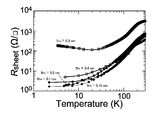
- Prior art keywords
- sto
- oxide film
- metal oxide
- metal
- type region
- Prior art date
- Legal status (The legal status is an assumption and is not a legal conclusion. Google has not performed a legal analysis and makes no representation as to the accuracy of the status listed.)
- Ceased
Links
Images















Classifications
-
- H—ELECTRICITY
- H10—SEMICONDUCTOR DEVICES; ELECTRIC SOLID-STATE DEVICES NOT OTHERWISE PROVIDED FOR
- H10D—INORGANIC ELECTRIC SEMICONDUCTOR DEVICES
- H10D30/00—Field-effect transistors [FET]
- H10D30/01—Manufacture or treatment
- H10D30/061—Manufacture or treatment of FETs having Schottky gates
-
- H—ELECTRICITY
- H10—SEMICONDUCTOR DEVICES; ELECTRIC SOLID-STATE DEVICES NOT OTHERWISE PROVIDED FOR
- H10D—INORGANIC ELECTRIC SEMICONDUCTOR DEVICES
- H10D30/00—Field-effect transistors [FET]
- H10D30/40—FETs having zero-dimensional [0D], one-dimensional [1D] or two-dimensional [2D] charge carrier gas channels
- H10D30/47—FETs having zero-dimensional [0D], one-dimensional [1D] or two-dimensional [2D] charge carrier gas channels having two-dimensional [2D] charge carrier gas channels, e.g. nanoribbon FETs or high electron mobility transistors [HEMT]
-
- H—ELECTRICITY
- H10—SEMICONDUCTOR DEVICES; ELECTRIC SOLID-STATE DEVICES NOT OTHERWISE PROVIDED FOR
- H10D—INORGANIC ELECTRIC SEMICONDUCTOR DEVICES
- H10D30/00—Field-effect transistors [FET]
- H10D30/80—FETs having rectifying junction gate electrodes
- H10D30/87—FETs having Schottky gate electrodes, e.g. metal-semiconductor FETs [MESFET]
-
- H—ELECTRICITY
- H10—SEMICONDUCTOR DEVICES; ELECTRIC SOLID-STATE DEVICES NOT OTHERWISE PROVIDED FOR
- H10D—INORGANIC ELECTRIC SEMICONDUCTOR DEVICES
- H10D62/00—Semiconductor bodies, or regions thereof, of devices having potential barriers
- H10D62/10—Shapes, relative sizes or dispositions of the regions of the semiconductor bodies; Shapes of the semiconductor bodies
-
- H—ELECTRICITY
- H10—SEMICONDUCTOR DEVICES; ELECTRIC SOLID-STATE DEVICES NOT OTHERWISE PROVIDED FOR
- H10D—INORGANIC ELECTRIC SEMICONDUCTOR DEVICES
- H10D62/00—Semiconductor bodies, or regions thereof, of devices having potential barriers
- H10D62/80—Semiconductor bodies, or regions thereof, of devices having potential barriers characterised by the materials
- H10D62/83—Semiconductor bodies, or regions thereof, of devices having potential barriers characterised by the materials being Group IV materials, e.g. B-doped Si or undoped Ge
-
- H—ELECTRICITY
- H10—SEMICONDUCTOR DEVICES; ELECTRIC SOLID-STATE DEVICES NOT OTHERWISE PROVIDED FOR
- H10D—INORGANIC ELECTRIC SEMICONDUCTOR DEVICES
- H10D8/00—Diodes
-
- H—ELECTRICITY
- H10—SEMICONDUCTOR DEVICES; ELECTRIC SOLID-STATE DEVICES NOT OTHERWISE PROVIDED FOR
- H10D—INORGANIC ELECTRIC SEMICONDUCTOR DEVICES
- H10D8/00—Diodes
- H10D8/50—PIN diodes
Definitions
- the present invention relates to a semiconductor device.
- Semiconductor devices such as transistors, diodes, light emitting diodes, optical sensors and solar cells are configured by utilizing the junction of n-type semiconductors and p-type semiconductors.
- impurities are doped into a Si substrate (wafer) to form a p-type semiconductor (p-type region) and an n-type semiconductor (n-type region).
- the mainstream of impurity doping is ion implantation in which a beam of atoms, which is an impurity, is implanted into a semiconductor substrate.
- the current ion implantation method destroys crystals on the Si substrate by colliding ions with high energy with the Si substrate.
- impurities diffuse in the depth direction, so that there is a limit to the formation of low-resistance n-type and p-type regions. Further, the high temperature heat treatment hinders the cost reduction of the semiconductor device.
- STO selectiveium titanate: SrTIO 3
- STO is a standard substrate.
- STO is useful because it has much higher mobility than Si and Ge.
- Non-Patent Document 5 reports that a very thin n-type region (that is, two-dimensional electron gas 2DEG) is formed at the interface between the STO and the metal by vacuum-depositing the metal on the STO substrate at room temperature. Has been done. This technique has the advantages that an expensive ion implanter can be replaced with an inexpensive vacuum vapor deposition apparatus and that high temperature treatment is not required.
- n-type region that is, two-dimensional electron gas 2DEG
- the present invention has been made in view of the above problems, and an exemplary purpose of the embodiment is to provide an STO semiconductor device provided with a p-type region.
- the STO semiconductor device is a p-type region formed on an STO substrate, a first metal oxide film formed on the STO substrate and having a thickness smaller than a predetermined threshold value, and an interface between the STO substrate and the first metal oxide film. And.
- Another aspect of the present invention relates to a method for manufacturing an STO (SrTIO 3 ) semiconductor device.
- This manufacturing method includes a step of depositing a first metal film having a thickness smaller than a predetermined threshold value on a portion of the STO substrate on which a p-type region should be formed, and a step of oxidizing the first metal film to form a first metal film.
- a step of forming a p-type region is provided at the interface between the STO substrate and the STO substrate.
- a p-type region can be formed on an STO semiconductor device.
- FIG. 4 (a) is an RHEED (reflection high energy electron diffraction) during the manufacturing process (in-Situ)
- FIG. 4 (b) is a scanning transmission electron microscope (STEM) image of the sample A10.
- 5 (a) and 5 (b) are diagrams showing the measurement results of samples A20, A40, and A60 by X-ray photoelectron spectroscopy (XPS).
- FIG. 6 (a) to 6 (e) are diagrams showing the measurement results of the Hall effect of the samples A10 to A40. It is a figure which shows the measurement result of the sheet resistance of samples A10 to A40.
- FIG. 8 (a) is a diagram showing the measurement results of the mobility ⁇ of the samples A10 to A40, and FIG. 8 (b) shows the film thickness (t) of the mobility (left axis) and the sheet carrier density (right axis). It is a figure which shows the measurement result of Fe) dependence.
- FIG. 9 (a) is a diagram showing the relationship between the reciprocal B -1 of the external magnetic field and the change d 2 R xx / dB 2 of the sheet resistance R xx in the sample A10, and FIG.
- FIG. 9 (b) is a diagram showing the relationship between the vertical magnetic field and the vertical magnetic field. It is a figure which shows the spectrum when B // [001] and the in-plane magnetic field B // [100] are applied. It is a figure which plotted the work function ⁇ and the oxide formation enthalpy change ⁇ H f of a metal element M of a typical element M. It is an equivalent circuit diagram of the STO semiconductor device of FIG. It is sectional drawing of the semiconductor device which concerns on Example 1.
- FIG. It is a figure explaining the manufacturing method of the STO semiconductor device of FIG. It is sectional drawing of the semiconductor device which concerns on Example 2.
- FIG. is sectional drawing of the STO semiconductor device which concerns on Example 3.
- FIG. It is sectional drawing of the semiconductor device which concerns on Example 4.
- FIG. It is sectional drawing of the FET which concerns on Example 5.
- FIG. It is a figure which shows the I DS- V GS curve (measurement result) of the FET of FIG.
- FIG. It is a figure which shows the I DS- V DS curve (measurement result) of the FET of FIG.
- FIG. Figure 21 (a)
- ⁇ (c) is a diagram showing the I DS -V DS characteristics of the FET of FIG. 17 (measurement result).
- FIG. Figure 23 (a) ⁇ (c) is a diagram showing the I DS -V DS characteristics of the FET of FIG.
- FIG. 22 (measurement result).
- 24 (a) to 24 (d) are diagrams showing the measurement results of the Hall effect of the FET of FIG. 22.
- FIG. 25 (a) is a diagram showing the relationship between the back gate voltage V BG and the Hall resistance R yx
- FIG. 25 (b) is a diagram showing the relationship between the back gate voltage V BG and the carrier density. It is a figure which shows the back gate voltage dependence of the hole mobility ⁇ Hall of FIG. 17 of FIG. It is a band diagram of FET which concerns on embodiment. It is a figure which shows the measurement result of the Hall effect of the FET of FIG. Figure 29 (a) ⁇ (c) are diagrams showing the dependence of the back gate voltage V BG of the FET of Figure 17.
- FIG. 25 (a) is a diagram showing the relationship between the back gate voltage V BG and the Hall resistance R yx
- FIG. 25 (b) is a diagram showing the relationship between the back gate voltage V BG and the carrier density. It is a figure
- FIG. 30A is a diagram showing the temperature dependence of the FET of FIG. 17, and FIG. 30B is a diagram showing the temperature dependence of the FET of FIG. 22.
- 31 (a) to 31 (d) are cross-sectional views of FETs according to Examples 7 to 10.
- FIG. 1 is a cross-sectional view showing the structure of the STO semiconductor device 100.
- the STO semiconductor device 100 includes an STO substrate 102, a metal oxide film 104, a p-type region 106, and a cap layer 108.
- the metal oxide film 104 is formed on the STO substrate 102.
- the metal oxide film 104 has a thickness t M smaller than a predetermined threshold value t TH .
- the p-type region 106 is a two-dimensional hall gas (2DHG) and is formed at the interface between the metal oxide film 104 and the STO substrate 102.
- the threshold value t TH will be described later.
- the cap layer 108 is formed on the metal oxide film 104 in order to stabilize the chemical properties of the device.
- the cap layer 108 can be a metal oxide film like the metal oxide film 104. It should be noted that the cap layer 108 is not an essential configuration for realizing the semiconductor characteristics.
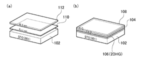
- FIG. 2A and 2 (b) are diagrams showing a manufacturing method of the STO semiconductor device 100.
- the metal film 110 is formed by depositing a metal element (here, Fe) on the STO substrate 102 under vacuum. Further, another metal element (here, Al) is deposited on the metal film 110 to form the metal film 112.
- a metal element here, Fe
- another metal element here, Al
- the metal element (Fe) contained in the metal film 110 deprives the STO substrate 102 of the oxygen element and oxidizes due to its high oxygen affinity, so that the metal film 110 of FIG. 2 (a) becomes the metal film 110 of FIG. 2 (b). It becomes a metal oxide film 104 (FeO x). Further, the metal element (Al) contained in the metal film 112 is also oxidized to form the cap layer 108 of the metal oxide film.
- the above is the basic configuration and manufacturing method of the STO semiconductor device 100 having a p-type region. Next, the reason why the p-type region is formed will be described.
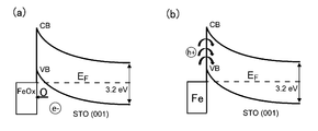
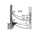
- 3 (a) and 3 (b) are band diagrams of the interface between the STO semiconductor device 100 and the metal oxide film 104 (metal film 110).
- FIG. 3 (a) shows the oxidation process.
- oxygen O is taken from the STO substrate 102.
- the amount of oxygen increases, the amount of oxygen deficiency in the STO substrate 102 increases.
- a two-dimensional electron gas (2DEG) that is, an n-type region is formed at the interface between the STO substrate 102 and the metal oxide film 104 by increasing the amount of oxygen deficiency.
- 2DEG two-dimensional electron gas
- the present inventors have focused on the fact that a process (hereinafter referred to as a bonding process) different from the oxidation process occurs with respect to the charge transfer at the interface between the STO substrate 102 and the metal film 110.
- FIG. 3 (b) When the STO ((001) plane) and the metal M are joined as shown in FIG. 3 (b), holes h + are supplied from the metal M to the STO. Further, the conduction band CB and the valence band VB are bent due to the difference in the work function ⁇ between the metal M and STO.
- the joining process of FIG. 3 (b) occurs prior to the oxidation process of FIG. 3 (a). Ignoring the oxidation process of the metal M in FIG. 3 (a), the joining process should form a two-dimensional whole gas (2DHG), or p-type region, in the STO.
- 2DHG two-dimensional whole gas
- the present inventors have decided that the bonding process of FIG. 3 (b) does not depend on the film thickness t M of the metal M, while the oxidation process of FIG. 3 (a) depends on the film thickness t M of the metal M. Attention is paid, and therefore, in the region where the film thickness t M is large, the oxidation process becomes dominant and an n-type region is formed, and when the film thickness t M is reduced, the joining process becomes dominant and a p-type region is formed. I came to realize that. That is, which of the two processes becomes dominant depends on the film thickness t M of the metal film 110, and it can be said that there is a threshold value t TH that is a boundary between the p-type and the n-type. .. In the STO semiconductor device 100 of FIG. 1, a p-type region can be formed by making the film thickness t M of the metal film 110 (metal oxide film 104) smaller than the threshold value t TH.
- a metal film 110 of Fe having a thickness of t Fe was vapor-deposited on the (001) surface of the STO substrate 102, and a metal film 112 of Al having a thickness of 1 nm was deposited on the metal film 110.
- Deposition temperature T S 50 °C
- background pressure is approximately 10 -8 Pa.
- six samples A10 to A60 having a thickness t Fe of the metal film 110 of 0.1, 0.15, 0.2, 0.3, 0.4, 0.6 nm were prepared, and their characteristics. Was evaluated.
- the metal film 110 and the metal film 112 are oxidized to become the metal oxide film 104 and the cap layer 108.
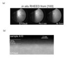
- FIG. 4 (a) is RHEED (reflection high energy electron diffraction) during the manufacturing process (in-Situ), and
- FIG. 4 (b) is a scanning transmission electron microscope (STEM) image of sample A10.
- the STO surface is flat at the atomic level.
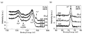
- FIG. 5 (a) and 5 (b) are diagrams showing the measurement results of samples A20, A40, and A60 by X-ray photoelectron spectroscopy (XPS).
- FIG. 5A shows the state of Fe
- FIG. 5B shows the state of Al.
- XPS X-ray photoelectron spectroscopy
- 6 (a) to 6 (e) are diagrams showing the measurement results of the Hall effect of the samples A10 to A40.
- the horizontal axis represents the applied magnetic field
- the vertical axis represents the Hall resistance R xy .
- the hole resistance R xy shows a straight line rising to the right, which confirms that the p-type semiconductor can be formed.
- the Hall resistance R xy is downward-sloping and shows non-linearity. This indicates that p-type and n-type are mixed.
- the hole resistance R xy is a straight line with a downward slope to the right, indicating that it is n-type. From FIGS.
- the carrier type in the STO substrate 102 can be selectively controlled by p-type and n-type according to the film thickness t Fe of the metal oxide film 104.
- the p-type region is formed by setting 0.3 nm as the threshold value t TH and t Fe ⁇ t TH
- the n-type region is formed by setting t Fe > t TH. It should be noted that this threshold value t TH is determined according to the type of element and the conditions of vapor deposition.
- FIG. 7 is a diagram showing the measurement results of the sheet resistance of the samples A10 to A40.
- Samples A10, A15, A20 in which the p-type region is formed, or sample A40 in which the n-type region is formed have substantially similar sheet resistance, and a sample in which the p-type region and the n-type region coexist. In A30, the sheet resistance is large.
- FIG. 8B is a diagram showing measurement results of film thickness (tFe ) dependence of mobility (left axis) and sheet carrier density (right axis).
- the p-type property is obtained at t Fe ⁇ 0.2 nm, and the n-type property is obtained at t Fe ⁇ 0.4 nm. Therefore, it can be said that the above-mentioned threshold value t TH exists between 0.2 nm and 0.4 nm. ..
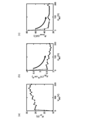
- FIG. 9A is a diagram showing the relationship between the reciprocal B -1 of the external magnetic field and the change d 2 R xx / dB 2 of the sheet resistance R xx in the sample A10.
- FIG. 9B is a diagram showing spectra when a vertical magnetic field B // [001] and an in-plane magnetic field B // [100] are applied. Only when the magnetic field B // [001] in the [001] direction, that is, the direction perpendicular to the surface of the STO substrate, is applied, the Shubnikov-de Haas oscillation is observed, and the magnetic field is observed in the [100] direction, that is, the in-plane direction of the STO substrate. This vibration was not observed when B // [100] was applied. This measurement result confirms that the holes are confined in the two-dimensional system of the STO substrate, that is, 2DHG is formed.
- the selection of the metal element M of the metal oxide film 104 can be determined in consideration of the second condition and the third condition described later.
- the metal M causes a large amount of oxygen deficiency during STO and generates many electron carriers, thereby realizing p-type conduction. Hinder. From this point of view, as the metal element M, it is preferable to select an element having an oxide formation enthalpy change ⁇ H f of ⁇ 8 eV / O 2 to -4.8 eV / O 2.
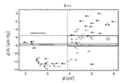
- FIG. 10 is a diagram in which the work function ⁇ of the representative element M and the oxide formation enthalpy change ⁇ H f of the metal element M are plotted.
- the metal element M contained in the solid line (i) Specifically, in addition to Fe, W (tungsten), Mo (molybdenum), V (vanadium), Mn (manganese), Cr (chromium), Nb (niobium) and the like may be used.
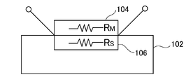
- FIG. 11 is an equivalent circuit diagram of the STO semiconductor device 100 of FIG.
- the two-terminal device is represented as a parallel connection circuit of the metal oxide film 104 and the p-type region 106.
- the resistance value R M of the metal oxide film 104 is too small, p-type region 106 is bypassed, it disappears characteristics as a semiconductor device.
- the resistance value R M of the metal oxide film 104 is sufficiently higher than the resistance value R S of the p-type region 106 is obtained.
- the sheet resistance of the metal oxide film 104 is preferably greater than 10 times the sheet resistance of the p-type region 106, and is 100 ⁇ / ⁇ or more. It is good to choose metal M.
- the actual semiconductor device is not a two-terminal device as shown in FIG. 11, but has a more complicated configuration including a pn junction, and the fourth condition may be relaxed depending on the configuration of the semiconductor device. is there.
- Fe used in the above sample satisfies all the first to fourth conditions.
- FIG. 12 is a cross-sectional view of the semiconductor device 200 according to the first embodiment.
- the semiconductor device 200 includes an STO substrate 202, a first metal oxide film 204, a second metal oxide film 206, a cap layer 208, a p-type region 210, and an n-type region 212.
- the first metal oxide film 204 is formed on the STO substrate 202 and has a thickness t M1 ( ⁇ t TH ) smaller than a predetermined threshold value t TH. Therefore, a p-type region 210 is formed at the interface between the STO substrate 202 and the first metal oxide film 204.
- the threshold value t TH is unique to the metal element constituting the first metal oxide film 204.
- the second metal oxide film 206 is formed on the STO substrate 202 adjacent to the first metal oxide film 204.
- the second metal oxide film 206 has a thickness t M2 larger than the first metal oxide film 204 and the threshold value t TH (t M2 > t TH ). Therefore, an n-type region 212 is formed at the interface between the STO substrate 202 and the second metal oxide film 206.
- the cap layer 208 is configured to cover the first metal oxide film 204 and the second metal oxide film 206.
- the first metal oxide film 204 and the second metal oxide film 206 contain the same metal element, and the p-type region 210 and the n-type region 212 are selectively formed by controlling the film thickness t. Can be done.
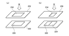
- FIG. 13 is a diagram illustrating a method of manufacturing the STO semiconductor device 200 of FIG.
- a metal element having a first film thickness t M1 is vapor-deposited, and the metal film 220 is deposited.
- the manufacturing method of the STO semiconductor device 200 is not limited to that shown in FIG.
- a mask in which only the region containing the first metal oxide film 204 is opened is used to deposit a metal element having a first film thickness t M1 and only the region containing the second metal oxide film 206 is opened. May be used to deposit a metal element having a thickness of t M2.
- FIG. 14 is a cross-sectional view of the semiconductor device 300 according to the second embodiment.
- the STO semiconductor device 300 includes an STO substrate 302, a first metal oxide film 304, a second metal oxide film 306, a cap layer 308, a p-type region 310, and an n-type region 312.
- the first metal oxide film 304 and the second metal oxide film 306 contain the same metal element.
- the first metal oxide film 304 has a thickness t M1 smaller than the threshold value t TH , and therefore a p-type region 310 is formed at the interface between the first metal oxide film 304 and the STO substrate 302.
- a metal film having a constant film thickness is formed on a portion corresponding to the first metal oxide film 304 and the second metal oxide film 306.
- a p-type region is formed at the interface between the metal film and the STO substrate 302.
- only the region corresponding to the n-type region 312 is selectively heated by laser irradiation or the like to selectively promote the oxidation of the portion of the metal film corresponding to the n-type region 312.
- the heated portion changes to the n-type region, while the unheated portion maintains the p-type.
- a metal film is formed on the portion corresponding to the second metal oxide film 306 so that the film thickness is t M2.
- an n-type region 312 is formed.
- a metal film is formed on the portion corresponding to the first metal oxide film 304 by vacuum vapor deposition at room temperature so that the film thickness is t M1.
- a p-type region is formed at the interface between the metal film and the STO substrate 302.
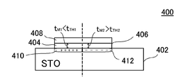
- FIG. 15 is a cross-sectional view of the STO semiconductor device 400 according to the third embodiment.
- the first metal oxide film and the second metal oxide film contain the same metal element, but this is not the case.
- the STO semiconductor device 400 includes an STO substrate 402, a first metal oxide film 404, a second metal oxide film 406, a cap layer 408, a p-type region 410, and an n-type region 412.
- the first metal oxide film 404 contains a first metal element
- the second metal oxide film 406 contains a second metal element different from the first metal element.
- the first metal oxide film 404 has a thickness t M1 smaller than the threshold value t TH1 peculiar to the first metal element, and therefore, a p-type region is formed at the interface between the first metal oxide film 404 and the STO substrate 402. 410 is formed.
- the second metal oxide film 406 has a thickness t M2 larger than the threshold value t TH2 peculiar to the second metal element, and therefore, an n-type region is formed at the interface between the second metal oxide film 406 and the STO substrate 402. 412 is formed.
- the magnitude relationship between t M1 and t M2 is determined according to the type of metal.
- FIG. 16 is a cross-sectional view of the semiconductor device 500 according to the fourth embodiment.
- the first metal oxide film 504 and the second metal oxide film 506 are formed on different surfaces of the STO substrate 502.
- a cap layer 508 is formed on the first metal oxide film 504, and a cap layer 509 is formed on the second metal oxide film 506. Then, the p-type region 510 and the n-type region 512 are joined in the vertical direction.
- STO semiconductor device As above is an example of the STO semiconductor device. According to those skilled in the art, it is understood that various devices such as transistors, diodes, light emitting diodes, optical sensors and solar cells can be configured by combining the p-type region and the n-type region, and the application of the present invention is specific. It is not limited to the use of.
- FET Field Effect Transistor
- FIG. 17 is a cross-sectional view of the FET 600 according to the fifth embodiment.
- the basic structure of the FET 600 is as described above, and includes an STO substrate 602, a metal oxide film 604, a p-type region 606, and a cap layer 608.
- the STO substrate 602 used was an easily available substrate having a thickness of 500 ⁇ m.
- the thickness t M of the metal oxide film 604 is 0.75 ⁇ , which is thinner than the above-mentioned threshold value t TH , and therefore, a p-type region 606 (two-dimensional Hall gas 2DHG) is formed under the metal oxide film 604. Will be done.
- the cap layer 608 formed on the upper side of the metal oxide film 604 is aluminum oxide (AlO x ) having a thickness of 1 nm.
- the length of the metal oxide film 604, that is, the channel length (gate length) L is 0.6 mm
- the width of the metal oxide film 604, that is, the channel width (gate width) W is 0.1 mm.
- the FET 600 has a back gate structure, and further includes a drain electrode 620, a source electrode 622, and a back gate electrode 624.
- the drain electrode 620 and the source electrode 622 are formed in a region adjacent to the metal oxide film 604 of the STO substrate 602.
- the drain electrode 620 and the source electrode 622 are, for example, aluminum and can be formed by metal deposition.
- N-type regions (two-dimensional electron gas 2DEG) 626,628 are formed directly below the drain electrode 620 and the source electrode 622.
- the back gate electrode 624 is also made of aluminum and can be formed by metal vapor deposition on the back surface side of the STO substrate 602. Since the drain and the source of this device are symmetrical, the names of the drain and the source are only for convenience.
- FIG. 19 is a diagram showing an I DS- V DS curve (measurement result) of the FET 600 of FIG.
- FIG. 20 is a diagram showing an I DS- V DS curve (measurement result) of the FET 600 of FIG. Only the range of -7V ⁇ V GS ⁇ -4.5V is plotted. The gate-source voltage V GS is at lower than -4.5V regions, negative resistance is observed. As shown in FIG. 17, a PN junction occurs between the n-type region 626 directly below the drain electrode 620 and the p-type region 606, which is a channel region, and a so-called Esaki diode is generated. Similarly, a PN junction is formed between the n-type region 628 directly below the source electrode 622 and the p-type region 606, which is a channel region, and an Esaki diode is formed.
- the negative resistance seen in FIG. 20 can be explained by the fact that the FET 600 behaves as a tunnel FET device.
- Figure 21 (a) ⁇ (c) is a diagram showing the FET600 of I DS -V DS characteristics of FIG. 17 (measurement result).
- FIG. 22 is a cross-sectional view of the FET 700 according to the sixth embodiment.
- the FET 700 includes an STO substrate 702, a metal oxide film 704, an n-type region 706, and a cap layer 708.
- the thickness t M of the metal oxide film 704 is 4 ⁇ , which is thicker than the above-mentioned threshold value t TH , and therefore an n-type region 706 (two-dimensional electron gas 2DEG) is formed under the metal oxide film 704.
- the cap layer 708 formed on the upper side of the metal oxide film 704 is aluminum oxide (AlO x ) having a thickness of 1 nm.
- the FET 700 has a back gate structure, and further includes a drain electrode 720, a source electrode 722, and a back gate electrode 724.
- the drain electrode 720 and the source electrode 722 are formed in a region adjacent to the metal oxide film 704 of the STO substrate 702.
- the drain electrode 720 and the source electrode 722 are, for example, aluminum and can be formed by metal deposition.
- an n-type region (two-dimensional electron gas 2DEG) 726,728 is formed. Therefore, the PN junction described in Example 5 does not exist.
- the back gate electrode 724 is also made of aluminum and can be formed by metal vapor deposition on the back surface side of the STO substrate 702. Since the drain and the source of this device are symmetrical, the names of the drain and the source are only for convenience.
- Figure 23 (a) ⁇ (c) is a diagram showing the I DS -V DS characteristics of FET700 of FIG. 22 (measurement result). As shown in FIGS. 23 (b) and 23 (c), no tunnel effect is observed. This is consistent with the absence of a PN junction between the drain and channel regions and between the source and channel regions in the FET 700 of FIG.
- 24 (a) to 24 (d) are diagrams showing the measurement results of the Hall effect of the FET 700 of FIG. 22. Measurements gate-source voltage V GS, i.e. went back gate voltage V BG is changed from 0,2,3,4,6,10,15,20,40,45,50,60V.
- FIG. 24 (b) is a plot of the characteristics when the back gate voltage V BG is 0, 2, 3, 4, 6, 10 V
- FIG. 24 (c) is a plot of the characteristics when the back gate voltage V BG is 15, 20, 20.
- FIG 24 (d) the back gate voltage V BG is a plot when the 50,60V.
- FIG. 25 (a) is a diagram showing the relationship between the back gate voltage V BG and the Hall resistance R yx
- FIG. 25 (b) is a diagram showing the relationship between the back gate voltage V BG and the carrier density.
- FIG. 25 (b) shows.
- the carrier type is n type.
- the carrier type changes from n type to p type.
- FIG. 26 is a diagram showing the back gate voltage dependence of the hole mobility ⁇ Hall of the FET 600 of FIG.
- VBG backgate voltage
- the mobility ⁇ Hall of holes which are carriers in the P-type region, and when it is raised from 0V to 200V, the mobility ⁇ Hall increases five times, and the high-speed operation of the transistor increases. You can expect it.
- FIG. 27 is a band diagram of the FET 600 of FIG.
- VBG positive backgate voltage
- the potential to bind holes two-dimensionally distributed to a shallow depth becomes steep, the hole concentration decreases, and the electron correlation weakens, which is a positive backgate. It is considered to be one of the causes that the mobility ⁇ Hall increases according to the voltage VBG.
- the decrease in interband scattering is also considered to be one of the factors that increase the mobility ⁇ Hall.
- FIG. 28 is a diagram showing a measurement result of the Hall effect of the FET 600 of FIG. The measurement was performed by changing the back gate voltage VBG from 0 V to 200 V.
- Figure 29 (a) ⁇ (c) is a diagram showing the dependence of the FET600 the back gate voltage V BG of Fig.
- FIG. 29 (a) shows the Hall resistance R yx
- FIG. 29 (b) shows the carrier density.
- Increasing the backgate voltage VBG increases the mobility ⁇ Hall, but decreases the carrier density.
- FIG. 29 (c) shows the sheet resistance, and the sheet resistance decreases by applying the gate voltage. This is a behavior different from that of a general transistor.
- FIG. 30 (a) is a diagram showing the temperature dependence of the FET 600 of FIG. 17, and FIG. 30 (b) is a diagram showing the temperature dependence of the FET 700 of FIG. 22. All FETs 600 and 700 were measured in an environment of 3.5,4,5,10,20,22,25,30,50K.
- the horizontal axis is the back gate voltage V BG
- the vertical axis is the drain current I DS .
- the thickness of the STO substrate is as thick as 500 ⁇ m. Therefore, the voltage range of the gate voltage V BG (that is, the gate-source voltage V GS ) is increased, but by using a thinner substrate or by adopting the front gate structure described in the seventh embodiment, Since the voltage range can be reduced, there is no problem in practical use. Similarly, the voltage range of the drain voltage V D (that is, the drain-source voltage V DS ) can be reduced by shortening the channel length.
- 31 (a) to 31 (d) are cross-sectional views of FETs 800A to 800D according to Examples 7 to 10.
- the FETs 800A to 800D commonly include an STO substrate 802, a metal oxide film 804 (or 805), a cap layer 808, a gate electrode 809, a drain electrode 820, and a source electrode 822.
- the FETs 800A to 800D have a front gate structure, and the gate electrode 809 is formed not on the back surface of the substrate 802 but on the upper surface of the cap layer 808.
- the cap layer 808 functions as an oxide insulating film, and therefore the FETs 800A to 800E have a MOS (Metal Oxide Semiconductor) structure.
- MOS Metal Oxide Semiconductor
- n-type region 823,828 is formed directly under each of the drain electrode 820 and the source electrode 822.
- the FET 800A of FIG. 31 (a) is a front gate of the FET 600 of FIG. 17, and the thickness of the metal oxide film 804 is thinner than the metal-specific threshold value t TH . Therefore, a p-type region is directly below the metal oxide film 804. 806 is formed.
- the FET 800B of FIG. 31 (b) is a front gate of the FET 700 of FIG. 22, and the thickness of the metal oxide film 805 is thicker than the metal-specific threshold value t TH. Region 807 is formed.
- the FETs 800C and 800D shown in FIGS. 31 (c) and 31 (d) are obtained by adding carrier type control electrodes 824 and 825 to the FET 800B shown in FIG. 31 (b).
- the carrier type control electrodes 824 and 825 are provided to apply an electric potential to the STO substrate from the outside.
- the carrier type control electrode 824 is formed on the back surface side of the STO substrate 802
- the carrier type control electrode 825 is formed on the front surface side of the STO substrate 802.
- VBG back gate voltage
- a back gate electrode may be provided in the same manner as the MOSFET having a front gate structure.
- the present invention relates to a semiconductor device.
- STO semiconductor device 102 STO substrate 104 metal oxide film 106 p-type region 108 cap layer 110, 112 metal film 200
- STO semiconductor device 202 STO substrate 204 first metal oxide film 206 second metal oxide film 208 cap layer 210 p-type region 212 n-type region 220 metal film 224 metal film 250 region 252 mask 254 region 256 mask 300
- STO semiconductor device 302 STO substrate 304 first metal oxide film 306 second metal oxide film 308 cap layer 310 p-type region 312 n-type region 400
- STO semiconductor Device 402 STO substrate 404 1st metal oxide film 406 2nd metal oxide film 408 Cap layer 410 p-type region 412 n-type region 500
- STO semiconductor device 502 STO substrate 504 1st metal oxide film 506 2nd metal oxide film 508,509 cap Layer 510 p-type region 512 n-type region 600
- FET 602 STO substrate 604
- Metal oxide film 606 p-type region 608 Cap layer
Landscapes
- Insulated Gate Type Field-Effect Transistor (AREA)
- Metal-Oxide And Bipolar Metal-Oxide Semiconductor Integrated Circuits (AREA)
Abstract
STO基板102に、金属酸化膜104が形成される。金属酸化膜104は、所定のしきい値tTHより小さい厚みtMを有する。STO基板102と金属酸化膜104の界面には、p型領域106が形成される。
Description
本発明は、半導体デバイスに関する。
トランジスタ、ダイオード、発光ダイオード、光センサや太陽電池などの半導体デバイスは、n型半導体とp型半導体との接合を利用して構成される。現在主流のシリコン(Si)プロセスでは、Si基板(ウェーハ)に不純物をドープし、p型半導体(p型領域)とn型半導体(n型領域)を形成する。不純物のドープは、不純物となる原子のビームを半導体基板に打ち込むイオン注入が主流である。
近年の半導体デバイスの高速化、微細化にともない、浅くかつ高濃度なn型およびp型領域を形成する技術が求められている。
現在のイオン注入方法は、高いエネルギーを有するイオンがSi基板に衝突することにより、Si基板の結晶を破壊する。破壊された結晶を高温の熱処理によって修復する際に、不純物が深さ方向に拡散することから、低抵抗なn型、p型領域の形成には限界がある。また高温の熱処理は、半導体デバイスのコスト削減の妨げとなる。
近年、高温超伝導材料、強磁性酸化物、強誘電体、高移動度材料などの分野で、酸化物エレクトロニクスが注目されており、その中で、STO(チタン酸ストロンチウム:SrTiO3)はスタンダード基板として用いられており、さまざまな研究成果が報告されている(非特許文献1~4参照)。STOは、SiやGeに比べて非常に高い移動度を有することから有用である。
非特許文献5には、STO基板上に、金属を室温で真空蒸着することにより、STOと金属の界面に、非常に薄いn型領域(すなわち二次元電子ガス2DEG)が形成されることが報告されている。この技術は、高価なイオン注入装置を、安価な真空蒸着装置に置換できること、また高温処理が不要であるといった利点がある。
Mannhart, J. & Schlom, D. G. , Science 327, pp1607-1611 (2010),"Oxide Interfaces-An Opportunity for Electronics"
D. Lu et al, Nature Mater. 15, 1255 (2016)
D. Ji et al., Nature 570, pp.87-90 (2019)
A. Ohtomo & H. Hwang, Nature 427, pp423-426 (2004)
P. Lomker et al., Phys. Rev. Mater. 1, 062001(R) (2017).
しかしながら、現在まで、STO基板上にp型領域を形成したという報告はなく、STO基板において、p-n接合を有する半導体デバイスは実現できていない。
本発明は係る課題に鑑みてなされたものであり、そのある態様の例示的な目的は、p型領域を備えるSTO半導体デバイスの提供にある。
本発明のある態様は、STO(SrTiO3)半導体デバイスに関する。STO半導体デバイスは、STO基板と、STO基板上に形成され、所定のしきい値より小さい厚みを有する第1金属酸化膜と、STO基板と第1金属酸化膜の界面に形成されるp型領域と、を備える。
本発明の別の態様は、STO(SrTiO3)半導体デバイスの製造方法に関する。この製造方法は、STO基板のp型領域を形成すべき部分に、所定のしきい値より小さい厚みを有する第1金属膜を蒸着するステップと、第1金属膜を酸化させ、第1金属膜とSTO基板の界面に、p型領域を形成するステップと、を備える。
なお、以上の構成要素の任意の組合せ、本発明の表現を装置、方法、システムなどの間で変換したものもまた、本発明の態様として有効である。
本発明によれば、STO半導体デバイス上にp型領域を形成できる。
(実施の形態)
以下、本発明を好適な実施の形態をもとに図面を参照しながら説明する。各図面に示される同一または同等の構成要素、部材、処理には、同一の符号を付するものとし、適宜重複した説明は省略する。また、実施の形態は、発明を限定するものではなく例示であって、実施の形態に記述されるすべての特徴やその組み合わせは、必ずしも発明の本質的なものであるとは限らない。
以下、本発明を好適な実施の形態をもとに図面を参照しながら説明する。各図面に示される同一または同等の構成要素、部材、処理には、同一の符号を付するものとし、適宜重複した説明は省略する。また、実施の形態は、発明を限定するものではなく例示であって、実施の形態に記述されるすべての特徴やその組み合わせは、必ずしも発明の本質的なものであるとは限らない。
また各図面における部材の寸法は、理解を容易にするために適宜拡大、縮小して示される。
(STO半導体基板上へのp型領域の形成)
上述のように、STO基板上にn型領域を形成した報告はあるが、p型領域を形成するには至っていない。そこではじめに、p型領域を備えるSTO半導体デバイスの基本構成を説明する。
上述のように、STO基板上にn型領域を形成した報告はあるが、p型領域を形成するには至っていない。そこではじめに、p型領域を備えるSTO半導体デバイスの基本構成を説明する。
図1は、STO半導体デバイス100の構造を示す断面図である。STO半導体デバイス100は、STO基板102、金属酸化膜104、p型領域106、キャップ層108を備える。金属酸化膜104は、STO基板102上に形成される。金属酸化膜104は、所定のしきい値tTHより小さい厚みtMを有する。p型領域106は二次元ホールガス(2DHG)であり、金属酸化膜104とSTO基板102の界面に形成される。しきい値tTHについては後述する。
キャップ層108は、デバイスの化学的特性の安定化のために、金属酸化膜104上に形成される。たとえばキャップ層108は、金属酸化膜104と同様に、金属酸化膜とすることができる。キャップ層108は、半導体特性を実現するために必須の構成ではないことに留意されたい。
図2(a)、(b)は、STO半導体デバイス100の製造方法を示す図である。図2(a)に示すように、金属元素(ここではFe)を、真空下でSTO基板102上に蒸着することにより金属膜110が形成される。さらに金属膜110の上に、別の金属元素(ここではAl)を蒸着することにより、金属膜112が形成される。
金属膜110に含まれる金属元素(Fe)が、その高い酸素親和力によって、STO基板102から酸素元素を奪い取って酸化することにより、図2(a)の金属膜110が、図2(b)の金属酸化膜104(FeOx)となる。また金属膜112に含まれる金属元素(Al)も酸化して金属酸化膜のキャップ層108が形成される。
以上が、p型領域を有するSTO半導体デバイス100の基本構成および製造方法である。続いてp型領域が形成される理由を説明する。
図3(a)、(b)は、STO半導体デバイス100と金属酸化膜104(金属膜110)の界面のバンド図である。
図3(a)には、酸化プロセスが示される。金属膜110内の金属元素が酸化して金属酸化膜104に変化する際に、STO基板102から酸素Oを奪い取る。この酸素の量が増えると、STO基板102中の酸素欠損の量が増える。酸素欠損は、電子キャリアを供給するドナーとして働くため、酸素欠損の量を増やすことにより、STO基板102と金属酸化膜104の界面に、二次元電子ガス(2DEG)、すなわちn型領域が形成される。非特許文献で報告されるSTO基板上のn型領域は、この酸化プロセスによって形成されている。
本発明者らは、STO基板102と金属膜110の界面における電荷移動に関して、酸化プロセスとは別のプロセス(以下、接合プロセスと称する)が生じていることに着目した。
図3(b)に示すようにSTO((001)面)と金属Mを接合すると、金属MからSTOに正孔h+が供給される。また金属MとSTOの仕事関数φの差から、伝導バンドCBと価電子バンドVBが曲げられる。図3(b)の接合プロセスは、図3(a)の酸化プロセスに先立って生じている。図3(a)の金属Mの酸化プロセスを無視すれば、STOには、接合プロセスによって、二次元ホールガス(2DHG)、すなわちp型領域が形成されるはずである。
本発明者らは、図3(b)の接合プロセスは、金属Mの膜厚tMには依存しない一方、図3(a)の酸化プロセスは金属Mの膜厚tMに依存することに着目し、したがって膜厚tMが大きい領域では、酸化プロセスが支配的となり、n型領域が形成され、膜厚tMを小さくすれば、接合プロセスが支配的となり、p型領域が形成されることを認識するに至った。つまり、2つのプロセスのいずれかが支配的となるかは、金属膜110の膜厚tMに応じて決まるものであり、p型とn型の境界となるしきい値tTHが存在すると言える。図1のSTO半導体デバイス100は、金属膜110(金属酸化膜104)の膜厚tMをしきい値tTHより小さくすることで、p型領域を形成することができている。
膜厚tMの依存性に関する実験結果を説明する。STO基板102の(001)面上に、厚みtFeのFeの金属膜110を蒸着し、その上に厚み1nmのAlの金属膜112を蒸着した。蒸着温度はTS=50℃、背景圧力は略10-8Paである。実験では、金属膜110の厚みtFeが、0.1,0.15,0.2,0.3,0.4,0.6nmである6個のサンプルA10~A60を作製し、その特性を評価した。上述のように金属膜110および金属膜112は酸化して金属酸化膜104、キャップ層108となる。
図4(a)は、製造プロセス中(in-Situ)のRHEED(反射高エネルギー電子線回折)であり、図4(b)は、サンプルA10の走査型透過電子顕微鏡(STEM)画像である。STO表面は原子レベルで平坦である。
図5(a)、(b)は、サンプルA20,A40,A60のX線光電子分光法(XPS)による測定結果を示す図である。図5(a)はFeの状態を、図5(b)はAlの状態を示している。tFe≦0.4nmのサンプルでは、FeとAlは酸化されてアモルファスとなっていることがわかる。金属酸化膜104およびキャップ層108中において、Fe3+とAl3+となっている。
図6(a)~(e)は、サンプルA10~A40のホール効果の測定結果を示す図である。横軸は印加した磁界を、縦軸はホール抵抗Rxyを示す。サンプルA10,A15,A20では、ホール抵抗Rxyは右肩上がりの直線を示しており、p型半導体が形成できていることが裏付けられる。サンプルA30では、ホール抵抗Rxyは右肩下がりであり、また非線形性を示している。これは、p型とn型が混在していることを示す。サンプルA40では、ホール抵抗Rxyは右肩下がりの直線であり、n型であることを示す。図6(a)~(e)から、金属酸化膜104の膜厚tFeに応じて、STO基板102内のキャリアタイプを、p型とn型で選択的に制御できることがわかる。この例では、0.3nmをしきい値tTHとして、tFe<tTHとすることでp型領域を、tFe>tTHとすることでn型領域が形成されることが分かる。なおこのしきい値tTHは、元素の種類や蒸着の条件に応じて決まることに留意されたい。
図7は、サンプルA10~A40のシート抵抗の測定結果を示す図である。p型領域が形成されるサンプルA10,A15,A20、あるいはn型領域が形成されるサンプルA40では、概ね似たようなシート抵抗が得られており、p型領域とn型領域が混在するサンプルA30では、シート抵抗が大きくなっている。
図8(a)は、サンプルA10~A40の移動度μの測定結果を示す図である。実験結果から、tFe=0.1nmのサンプルA10では、2Kの低温状態において、24000cm2/Vsもの非常に大きな正孔の移動度μが実現できていることが分かる。
図8(b)は、移動度(左軸)とシートキャリア密度(右軸)の膜厚(tFe)依存性の測定結果を示す図である。tFe≦0.2nmにおいてp型の、tFe≧0.4nmにおいてn型の特性が得られており、したがって上述のしきい値tTHは0.2nmと0.4nmの間に存在すると言える。
図9(a)は、サンプルA10における、外部磁場の逆数B-1と、シート抵抗Rxxの変化d2Rxx/dB2の関係を示す図である。図9(b)は、垂直磁場B//[001]および面内磁場B//[100]を印加したときのスペクトルを示す図である。[001]方向、すなわちSTO基板の表面と垂直方向の磁場B//[001]を印加した場合のみ、Shubnikov-de Haas振動が観測され、[100]方向、すなわちSTO基板の面内方向に磁場B//[100]を印加した場合にはこの振動は観測されなかった。この測定結果は、正孔はSTO基板の二次元系に閉じ込められていること、すなわち2DHGが形成されていることを裏付ける。
続いて、図1のSTO半導体デバイス100を作製するための条件を説明する。これらの条件のいくつかは、STO半導体デバイス100の製造方法や用途などによっては、必ずしも必須とは限らないことに留意されたい。
(第1条件)
p型領域を有するSTO半導体デバイス100を、真空蒸着で作製する際には、真空蒸着の温度は300℃以下とすることが望ましい。これは蒸着時に、STOの酸素が真空中に放出し、酸素欠損が発生するのを抑制するためである。真空蒸着は室温30℃でも可能であるから、この条件は容易に満たすことができる。
p型領域を有するSTO半導体デバイス100を、真空蒸着で作製する際には、真空蒸着の温度は300℃以下とすることが望ましい。これは蒸着時に、STOの酸素が真空中に放出し、酸素欠損が発生するのを抑制するためである。真空蒸着は室温30℃でも可能であるから、この条件は容易に満たすことができる。
(第2条件)
金属酸化膜104の金属元素Mの選択に関しては、第2条件および後述の第3条件を考慮して決めることができる。
金属酸化膜104の金属元素Mの選択に関しては、第2条件および後述の第3条件を考慮して決めることができる。
図3(b)に示すように、金属MとSTOの接合において、バンドを曲げて、STOにホールを供給するためには、金属Mの仕事関数φが、STOのそれφSTO(3.9V)よりも十分に高いことが要求される。さらに酸化プロセスによって金属Mが酸化した後も、このバンドの曲がりは維持される必要があるから、酸化物MOxの仕事関数も、STOの仕事関数φSTO=3.9Vよりも十分に高いことが要求される。
(第3条件)
図2に示すように、STO基板102上に金属Mを含む金属膜110を蒸着した後、金属Mを酸化させて絶縁化する必要がある。金属Mを、図3(a)の酸化プロセスによって酸化物MOxに変化させるためには、金属元素Mの酸化物生成エンタルピー変化ΔHfの絶対値が、STOの酸素欠損形成エネルギー(4.8eV/酸素欠損)より大きいことが求められる。一方で、金属Mの酸化物生成エンタルピー変化ΔHfの絶対値が大き過ぎると、金属MがSTO中に大量の酸素欠損を発生させ、多くの電子キャリアを生成してしまいp型伝導の実現を妨げる。この観点から、金属元素Mは、その酸化物生成エンタルピー変化ΔHfが-8eV/O2~-4.8eV/O2の元素を選ぶとよい。
図2に示すように、STO基板102上に金属Mを含む金属膜110を蒸着した後、金属Mを酸化させて絶縁化する必要がある。金属Mを、図3(a)の酸化プロセスによって酸化物MOxに変化させるためには、金属元素Mの酸化物生成エンタルピー変化ΔHfの絶対値が、STOの酸素欠損形成エネルギー(4.8eV/酸素欠損)より大きいことが求められる。一方で、金属Mの酸化物生成エンタルピー変化ΔHfの絶対値が大き過ぎると、金属MがSTO中に大量の酸素欠損を発生させ、多くの電子キャリアを生成してしまいp型伝導の実現を妨げる。この観点から、金属元素Mは、その酸化物生成エンタルピー変化ΔHfが-8eV/O2~-4.8eV/O2の元素を選ぶとよい。
図10は、代表的な元素Mの、仕事関数φおよび金属元素Mの酸化物生成エンタルピー変化ΔHfをプロットした図である。第2条件および第3条件を考慮すると、実線(i)に含まれる金属元素Mを用いるとよい。具体的には、Feの他に、W(タングステン),Mo(モリブデン)、V(バナジウム)、Mn(マンガン)、Cr(クロム)、Nb(ニオブ)などを用いてもよい。
(第4条件)
図11は、図1のSTO半導体デバイス100の等価回路図である。STO半導体デバイス100を2端子デバイスとみなすとき、2端子デバイスは、金属酸化膜104とp型領域106の並列接続回路として表される。ここで金属酸化膜104の抵抗値RMが小さすぎると、p型領域106がバイパスされ、半導体デバイスとしての特性が見えなくなる。したがって金属酸化膜104の抵抗値RMは、p型領域106の抵抗値RSよりも十分に高いことが求められる。
図11は、図1のSTO半導体デバイス100の等価回路図である。STO半導体デバイス100を2端子デバイスとみなすとき、2端子デバイスは、金属酸化膜104とp型領域106の並列接続回路として表される。ここで金属酸化膜104の抵抗値RMが小さすぎると、p型領域106がバイパスされ、半導体デバイスとしての特性が見えなくなる。したがって金属酸化膜104の抵抗値RMは、p型領域106の抵抗値RSよりも十分に高いことが求められる。
p型領域106のシート抵抗は、~10Ω/□のオーダーであるから、金属酸化膜104のシート抵抗は、p型領域106のシート抵抗の10倍より大きいことが望ましく、100Ω/□以上となる金属Mを選ぶとよい。
なお実際の半導体デバイスは、図11のような2端子デバイスではなく、p-n接合を含むより複雑な構成を有しており、半導体デバイスの構成によっては、第4条件が緩和される場合もある。
上述のサンプルで用いたFeは、第1条件~第4条件をすべて満たしている。
実用上は、p領域とn領域の両方をSTO基板上に形成する必要がある。以下、p領域とn領域を備える半導体デバイスの実施例を説明する。
(実施例1)
図12は、実施例1に係る半導体デバイス200の断面図である。半導体デバイス200は、STO基板202、第1金属酸化膜204、第2金属酸化膜206、キャップ層208、p型領域210、n型領域212を備える。
図12は、実施例1に係る半導体デバイス200の断面図である。半導体デバイス200は、STO基板202、第1金属酸化膜204、第2金属酸化膜206、キャップ層208、p型領域210、n型領域212を備える。
第1金属酸化膜204は、STO基板202上に形成され、所定のしきい値tTHより小さい厚みtM1(<tTH)有する。したがって、STO基板202と第1金属酸化膜204の界面にはp型領域210が形成される。なおしきい値tTHは第1金属酸化膜204の構成する金属元素に固有のものである。
第2金属酸化膜206は、STO基板202上に、第1金属酸化膜204と隣接して形成される。第2金属酸化膜206は第1金属酸化膜204およびしきい値tTHより大きな厚みtM2を有する(tM2>tTH)。したがって、STO基板202と第2金属酸化膜206の界面には、n型領域212が形成される。
キャップ層208は、第1金属酸化膜204および第2金属酸化膜206を覆うように構成される。
実施例1では、第1金属酸化膜204と第2金属酸化膜206は同じ金属元素を含み、膜厚tを制御することにより、p型領域210とn型領域212を選択的に形成することができる。
図13は、図12のSTO半導体デバイス200の製造方法を説明する図である。たとえばSTO基板202上の第1金属酸化膜204と第2金属酸化膜206を含む領域250が開口されたマスク252を用いて、第1の膜厚tM1の金属元素を蒸着し、金属膜220を形成する。続いて、第2金属酸化膜206を含む領域254のみが開口されたマスク256を用いて、厚さΔt=tM2-tM1の金属元素を蒸着し、金属膜224を形成してもよい。
当業者によれば、STO半導体デバイス200の製造方法が図13のそれに限定されないことが理解される。たとえば、第1金属酸化膜204を含む領域のみが開口されたマスクを用いて、第1の膜厚tM1の金属元素を蒸着し、第2金属酸化膜206を含む領域のみが開口されたマスクを用いて、厚さtM2の金属元素を蒸着してもよい。
(実施例2)
図14は、実施例2に係る半導体デバイス300の断面図である。STO半導体デバイス300は、STO基板302、第1金属酸化膜304、第2金属酸化膜306、キャップ層308、p型領域310、n型領域312を備える。
図14は、実施例2に係る半導体デバイス300の断面図である。STO半導体デバイス300は、STO基板302、第1金属酸化膜304、第2金属酸化膜306、キャップ層308、p型領域310、n型領域312を備える。
第1金属酸化膜304および第2金属酸化膜306は、同じ金属元素を含む。第1金属酸化膜304は、しきい値tTHより小さい厚みtM1を有しており、したがって第1金属酸化膜304とSTO基板302の界面には、p型領域310が形成される。
第2金属酸化膜306は、第1金属酸化膜304と同じ金属元素を有し、同じ厚みtM2=tM1を有しているが、第2金属酸化膜306は、第1金属酸化膜304より多くの酸素を含んでいる。第2金属酸化膜306に含まれる酸素は、STO基板302から供給されたものであり、STO基板302の第2金属酸化膜306とオーバーラップする領域には、より多くの酸素欠損が生じることとなり、n型領域312が形成される。
図14のSTO半導体デバイス300の製造方法を説明する。
第1の製造方法では、はじめに、第1金属酸化膜304および第2金属酸化膜306に対応する部分に、膜厚が一定の金属膜を形成する。この状態では、この金属膜とSTO基板302の界面には、p型領域が形成される。続いて、n型領域312に対応する領域のみを、レーザ照射などによって選択的に加熱し、金属膜のn型領域312に対応する部分の酸化を選択的に促進させる。これにより、加熱された部分がn型領域に変化する一方、加熱されなかった部分はp型を維持する。
第2の製造方法では、はじめに第2金属酸化膜306に対応する部分に、膜厚がtM2となるように金属膜を形成する。この状態で加熱し、酸化を促進することで、n型領域312が形成される。続いて、室温で真空蒸着によって、第1金属酸化膜304に対応する部分に、膜厚がtM1となるように金属膜を形成する。これによりこの金属膜とSTO基板302の界面に、p型領域が形成される。
(実施例3)
図15は、実施例3に係るSTO半導体デバイス400の断面図である。実施例1、2では、第1金属酸化膜と第2金属酸化膜が同一の金属元素を含んだが、その限りでない。
図15は、実施例3に係るSTO半導体デバイス400の断面図である。実施例1、2では、第1金属酸化膜と第2金属酸化膜が同一の金属元素を含んだが、その限りでない。
STO半導体デバイス400は、STO基板402、第1金属酸化膜404、第2金属酸化膜406、キャップ層408、p型領域410、n型領域412を備える。
第1金属酸化膜404は、第1金属元素を含み、第2金属酸化膜406は第1金属元素とは異なる第2金属元素を含む。第1金属酸化膜404は、第1金属元素に固有のしきい値tTH1より小さい厚みtM1を有しており、したがって第1金属酸化膜404とSTO基板402の界面には、p型領域410が形成される。
第2金属酸化膜406は、第2金属元素に固有のしきい値tTH2より大きい厚みtM2を有しており、したがって第2金属酸化膜406とSTO基板402の界面には、n型領域412が形成される。実施例3では、tM1とtM2の大小関係は、金属の種類に応じて定まることとなる。
(実施例4)
実施例1~3では、第1金属酸化膜と第2金属膜がSTO基板の同一面に形成され、したがってp型領域とn型領域が横方向に接合されたが、その限りでない。図16は、実施例4に係る半導体デバイス500の断面図である。この半導体デバイス500において、第1金属酸化膜504と第2金属酸化膜506は、STO基板502の異なる面に形成される。第1金属酸化膜504の上にはキャップ層508が、第2金属酸化膜506の上にはキャップ層509が形成される。そして、p型領域510とn型領域512は縦方向に接合される。
実施例1~3では、第1金属酸化膜と第2金属膜がSTO基板の同一面に形成され、したがってp型領域とn型領域が横方向に接合されたが、その限りでない。図16は、実施例4に係る半導体デバイス500の断面図である。この半導体デバイス500において、第1金属酸化膜504と第2金属酸化膜506は、STO基板502の異なる面に形成される。第1金属酸化膜504の上にはキャップ層508が、第2金属酸化膜506の上にはキャップ層509が形成される。そして、p型領域510とn型領域512は縦方向に接合される。
以上がSTO半導体デバイスの実施例である。当業者によれば、p型領域とn型領域を組み合わせることにより、トランジスタ、ダイオード、発光ダイオード、光センサや太陽電池などさまざまなデバイスを構成しうることが理解され、本発明の適用は、特定の用途に限定されるものではない。
最後にSTO半導体デバイスの利点をまとめると、第1に、真空蒸着により製造できるため、低コスト化や大面積化が容易である。
第2に、高温工程が不要であるため、プラスチック基板などを用いてフレキシブルデバイスやフレキシブル回路を作製することも可能である。
第3に、同一のSTO基板上に、複数のトランジスタやダイオードなどを形成し、さらにそれらを接続する配線を、真空蒸着によって形成することが可能である。この場合、すべての工程を真空蒸着のみで行うことが可能となる。
第4に、非常に薄く、また電気伝導が良好なp型領域とn型領域を形成できるため、将来のより微細なデバイスへの適用が期待できる。
(電界効果トランジスタ)
上述の半導体デバイスの実証のために、FET(電界効果トランジスタ)を作成し、その特性を評価した。
上述の半導体デバイスの実証のために、FET(電界効果トランジスタ)を作成し、その特性を評価した。
(実施例5)
図17は、実施例5に係るFET600の断面図である。このFET600の基本構造は上述した通りであり、STO基板602、金属酸化膜604、p型領域606、キャップ層608を備える。原理実証を目的としているため、STO基板602は入手が容易な厚み500μmの基板を用いた。
図17は、実施例5に係るFET600の断面図である。このFET600の基本構造は上述した通りであり、STO基板602、金属酸化膜604、p型領域606、キャップ層608を備える。原理実証を目的としているため、STO基板602は入手が容易な厚み500μmの基板を用いた。
金属酸化膜604の厚みtMは、0.75Åであり、上述のしきい値tTHより薄く、したがって金属酸化膜604の下側には、p型領域606(二次元ホールガス2DHG)が形成される。金属酸化膜604の上側に形成されるキャップ層608は、厚さ1nmの酸化アルミニウム(AlOx)である。金属酸化膜604の長さ、すなわちチャンネル長(ゲート長)Lは0.6mm、金属酸化膜604の幅すなわちチャンネル幅(ゲート幅)Wは0.1mmである。
FET600は、バックゲート構造を有しており、ドレイン電極620、ソース電極622、バックゲート電極624をさらに備える。ドレイン電極620とソース電極622は、STO基板602の金属酸化膜604と隣接する領域に形成される。ドレイン電極620とソース電極622はたとえばアルミニウムであり、金属蒸着により形成することができる。ドレイン電極620とソース電極622の直下には、n型領域(二次元電子ガス2DEG)626,628が形成される。
バックゲート電極624もアルミニウムであり、STO基板602の裏面側に金属蒸着によって形成することができる。なおこのデバイスは、ドレインとソースが対称であるため、ドレイン、ソースの名称は便宜的なものに過ぎない。
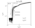
図18は、図17のFET600のIDS-VGS曲線(測定結果)を示す図である。測定は3.5Kという極低温で、ソース電圧VSを基準電位0Vとして、VDS(=VD-VS)=0.5Vの条件で行った。この条件下でのしきい値VTHは-7Vであり、ノーマリオンの特性が得られている。この曲線は、ヒステリシス特性を示しており、サブスレッショルドスイング値(S値)は、20.0mV/decおよび38.1mV/decであり、またオン・オフ比ION/IOFFは108であり、室温の最新のMOSFETと遜色ない特性が得られていることがわかる。
図19は、図17のFET600のIDS-VDS曲線(測定結果)を示す図である。ゲート電圧VGS(=VBG-VS)が、60,40,20,15,10,5,1,-1,-5,-10VのときのIV特性がプロットされており、左側の縦軸はリニアスケール、右側の縦軸はログスケールである。基本的には、ゲート電圧VGSを大きくするほど、ドレイン電流IDSは増加する傾向が見られる。
図20は、図17のFET600のIDS-VDS曲線(測定結果)を示す図である。-7V<VGS<-4.5Vの範囲のみをプロットしたものである。ゲートソース間電圧VGSが-4.5Vより低い領域では、負性抵抗が観測される。図17に示すように、ドレイン電極620の直下のn型領域626と、チャンネル領域であるp型領域606の間にPN接合が生じ、いわゆる江崎ダイオードが生成される。同様にソース電極622の直下のn型領域628と、チャンネル領域であるp型領域606の間にPN接合が生じ、江崎ダイオードが形成される。図20に見られる負性抵抗は、FET600がトンネルFETデバイスとして振る舞うことから説明できる。
図21(a)~(c)は、図17のFET600のIDS-VDS特性(測定結果)を示す図である。図21(c)は、VGS=-5.2Vの特性がプロットされており、逆バイアスにおける明確なトンネル効果が見られる。
(実施例6)
図22は、実施例6に係るFET700の断面図である。このFET700は、STO基板702、金属酸化膜704、n型領域706、キャップ層708を備える。STO基板702は入手が容易な厚み500μmの基板を用いた。
図22は、実施例6に係るFET700の断面図である。このFET700は、STO基板702、金属酸化膜704、n型領域706、キャップ層708を備える。STO基板702は入手が容易な厚み500μmの基板を用いた。
金属酸化膜704の厚みtMは4Åであり、上述のしきい値tTHより厚く、したがって金属酸化膜704の下側には、n型領域706(二次元電子ガス2DEG)が形成される。金属酸化膜704の上側に形成されるキャップ層708は、厚さ1nmの酸化アルミニウム(AlOx)である。
FET700は、バックゲート構造を有しており、ドレイン電極720、ソース電極722、バックゲート電極724をさらに備える。ドレイン電極720とソース電極722は、STO基板702の金属酸化膜704と隣接する領域に形成される。ドレイン電極720とソース電極722はたとえばアルミニウムであり、金属蒸着により形成することができる。ドレイン電極720とソース電極722の直下には、n型領域(二次元電子ガス2DEG)726,728が形成される。したがって、実施例5で説明したPN接合は存在しない。
バックゲート電極724もアルミニウムであり、STO基板702の裏面側に金属蒸着によって形成することができる。なおこのデバイスは、ドレインとソースが対称であるため、ドレイン、ソースの名称は便宜的なものに過ぎない。
図23(a)~(c)は、図22のFET700のIDS-VDS特性(測定結果)を示す図である。図23(b)、(c)に示すように、トンネル効果は見られない。これは、図22のFET700では、ドレインとチャンネル領域間、ソースとチャンネル領域間に、PN接合が存在しないことと整合する。
続いて、実施例6に係るFET700のキャリアタイプの制御について説明する。
図24(a)~(d)は、図22のFET700のホール効果の測定結果を示す図である。測定は、ゲートソース間電圧VGS、すなわちバックゲート電圧VBGを0,2,3,4,6,10,15,20,40,45,50,60Vと変化させて行った。
図24(b)は、バックゲート電圧VBGが0,2,3,4,6,10Vのときの特性のプロットであり、図24(c)は、バックゲート電圧VBGが15,20,40,45Vのときのプロットであり、図24(d)は、バックゲート電圧VBGが50,60Vのときのプロットである。
図25(a)は、バックゲート電圧VBGとホール抵抗Ryxの関係を示す図であり、図25(b)は、バックゲート電圧VBGとキャリア密度の関係を示す図である。
上述のように、金属酸化膜704の厚みtMがしきい値tTHより厚い場合、金属酸化膜704の直下には、n型領域が形成されることが分かっており、図25(b)に示すように、バックゲート電圧VBGが0~10Vの範囲では、キャリアタイプはn型となっている。ところが、バックゲート電圧VBGをさらに上昇させたところ、バックゲート電圧VBGが50Vを超えると、キャリアタイプがn型からp型に変化する。
つまり、従来では、金属酸化膜704が厚い場合、n型領域しか形成することしかできなかったが、高いバックゲート電圧VBGを印加することにより、金属酸化膜704の直下にp型領域を形成することができるようになるという知見が得られている。
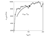
続いて、実施例5に戻り、図17のFET600のホール効果の測定結果を説明する。図26は、図17のFET600の正孔の移動度μHallのバックゲート電圧依存性を示す図である。バックゲート電圧VBGを高くするほど、P型領域のキャリアである正孔の移動度μHallが上昇し、0Vから200Vまで上昇させると、移動度μHallは5倍となり、トランジスタの高速動作が期待できる。
図27は、図17のFET600のバンド図である。正のバックゲート電圧VBGを与えると、浅い深さに二次元に分布する正孔を束縛するポテンシャルが急峻になり、正孔濃度が減少し、電子相関が弱くなることが、正のバックゲート電圧VBGに応じて移動度μHallが高くなる原因のひとつと考えられる。また量子準位の数が減少するので、バンド間散乱が減少することも、移動度μHallが高くなる要因のひとつと考えられる。
図28は、図17のFET600のホール効果の測定結果を示す図である。測定はバックゲート電圧VBGを0Vから200Vまで変化させて行った。
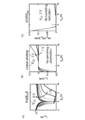
図29(a)~(c)は、図17のFET600のバックゲート電圧VBGの依存性を示す図である。図29(a)は、ホール抵抗Ryxを、図29(b)は、キャリア密度を示す。バックゲート電圧VBGを増加させると移動度μHallが増加する反面、キャリア密度は低下する。
図29(c)はシート抵抗を示し、ゲート電圧の印加により、シート抵抗は減少する。これは一般的なトランジスタとは異なる振る舞いである。
続いて、実施例5および実施例6に係るFET600,700の温度依存性を説明する。図30(a)は、図17のFET600の温度依存性を示す図であり、図30(b)は、図22のFET700の温度依存性を示す図である。いずれのFET600,700についても、3.5,4,5,10,20,22,25,30,50Kの環境で測定した。横軸はバックゲート電圧VBG、縦軸はドレイン電流IDSである。
実施例5,6では、バックゲート構造である上に、STO基板の厚みが500μmと厚い。そのために、ゲート電圧VBG(すなわちゲートソース間電圧VGS)の電圧レンジが大きくなっているが、より薄い基板を用いることにより、あるいは実施例7で説明するフロントゲート構造を採用することで、電圧レンジは小さくすることができため、実用上、問題となることはない。同様に、ドレイン電圧VD(すなわちドレインソース間電圧VDS)の電圧レンジについても、チャンネル長を短くすることで、小さくすることができる。
(実施例7)
図31(a)~(d)は、実施例7~実施例10に係るFET800A~FET800Dの断面図である。FET800A~800Dは、STO基板802、金属酸化膜804(または805)、キャップ層808、ゲート電極809、ドレイン電極820、ソース電極822を共通して備える。FET800A~800Dはフロントゲート構造を有しており、ゲート電極809は、基板802の裏面ではなく、キャップ層808の上面に形成される。このキャップ層808は酸化絶縁膜として機能し、したがってこのFET800A~800Eは、MOS(Metal Oxide Semiconductor)構造を有している。
図31(a)~(d)は、実施例7~実施例10に係るFET800A~FET800Dの断面図である。FET800A~800Dは、STO基板802、金属酸化膜804(または805)、キャップ層808、ゲート電極809、ドレイン電極820、ソース電極822を共通して備える。FET800A~800Dはフロントゲート構造を有しており、ゲート電極809は、基板802の裏面ではなく、キャップ層808の上面に形成される。このキャップ層808は酸化絶縁膜として機能し、したがってこのFET800A~800Eは、MOS(Metal Oxide Semiconductor)構造を有している。
またドレイン電極820、ソース電極822それぞれの直下には、n型領域826,828が形成される。
図31(a)のFET800Aは、図17のFET600をフロントゲート化したものであり、金属酸化膜804の厚みは、金属固有のしきい値tTHより薄く、したがってその直下には、p型領域806が形成される。
図31(b)のFET800Bは、図22のFET700をフロントゲート化したものであり、金属酸化膜805の厚みは、、金属固有のしきい値tTHより厚く、したがってその直下には、n型領域807が形成される。
図31(c)、(d)のFET800C、800Dは、図31(b)のFET800Bに、キャリアタイプ制御電極824、825を追加したものである。キャリアタイプ制御電極824,825は、STO基板に外部から電位を印加するために設けられる。図31(c)では、キャリアタイプ制御電極824は、STO基板802の裏面側に形成され、図31(d)では、キャリアタイプ制御電極825は、STO基板802の表面側に形成される。実施例6で説明したように、バックゲート電圧VBGすなわち基板電位を大きくすることで、ゲート直下のチャンネルのキャリアタイプを、n型とp型とで切りかえることが可能となる。
なお、図31(a)、(b)のFET800A,800Bのフロントゲート構造のFETにおいても、キャリアタイプを制御する目的ではなく、基板電位を電源電圧あるいは接地電圧に固定するために、一般的なフロントゲート構造のMOSFETと同様にバックゲート電極を設けてもよい。
実施の形態にもとづき、具体的な用語を用いて本発明を説明したが、実施の形態は、本発明の原理、応用を示しているにすぎず、実施の形態には、請求の範囲に規定された本発明の思想を逸脱しない範囲において、多くの変形例や配置の変更が認められる。
本発明は、半導体デバイスに関する。
100 STO半導体デバイス
102 STO基板
104 金属酸化膜
106 p型領域
108 キャップ層
110,112 金属膜
200 STO半導体デバイス
202 STO基板
204 第1金属酸化膜
206 第2金属酸化膜
208 キャップ層
210 p型領域
212 n型領域
220 金属膜
224 金属膜
250 領域
252 マスク
254 領域
256 マスク
300 STO半導体デバイス
302 STO基板
304 第1金属酸化膜
306 第2金属酸化膜
308 キャップ層
310 p型領域
312 n型領域
400 STO半導体デバイス
402 STO基板
404 第1金属酸化膜
406 第2金属酸化膜
408 キャップ層
410 p型領域
412 n型領域
500 STO半導体デバイス
502 STO基板
504 第1金属酸化膜
506 第2金属酸化膜
508,509 キャップ層
510 p型領域
512 n型領域
600 FET
602 STO基板
604 金属酸化膜
606 p型領域
608 キャップ層
620 ドレイン電極
622 ソース電極
624 バックゲート電極
626 n型領域
628 n型領域
700 FET
702 STO基板
704 金属酸化膜
706 n型領域
708 キャップ層
720 ドレイン電極
722 ソース電極
724 バックゲート電極
800A FET
800B FET
800C FET
800D FET
802 STO基板
804 金属酸化膜
805 金属酸化膜
806 p型領域
807 n型領域
808 キャップ層
809 ゲート電極
820 ドレイン電極
822 ソース電極
824,825 キャリアタイプ制御電極
826,828 n型領域
102 STO基板
104 金属酸化膜
106 p型領域
108 キャップ層
110,112 金属膜
200 STO半導体デバイス
202 STO基板
204 第1金属酸化膜
206 第2金属酸化膜
208 キャップ層
210 p型領域
212 n型領域
220 金属膜
224 金属膜
250 領域
252 マスク
254 領域
256 マスク
300 STO半導体デバイス
302 STO基板
304 第1金属酸化膜
306 第2金属酸化膜
308 キャップ層
310 p型領域
312 n型領域
400 STO半導体デバイス
402 STO基板
404 第1金属酸化膜
406 第2金属酸化膜
408 キャップ層
410 p型領域
412 n型領域
500 STO半導体デバイス
502 STO基板
504 第1金属酸化膜
506 第2金属酸化膜
508,509 キャップ層
510 p型領域
512 n型領域
600 FET
602 STO基板
604 金属酸化膜
606 p型領域
608 キャップ層
620 ドレイン電極
622 ソース電極
624 バックゲート電極
626 n型領域
628 n型領域
700 FET
702 STO基板
704 金属酸化膜
706 n型領域
708 キャップ層
720 ドレイン電極
722 ソース電極
724 バックゲート電極
800A FET
800B FET
800C FET
800D FET
802 STO基板
804 金属酸化膜
805 金属酸化膜
806 p型領域
807 n型領域
808 キャップ層
809 ゲート電極
820 ドレイン電極
822 ソース電極
824,825 キャリアタイプ制御電極
826,828 n型領域
Claims (14)
- STO(SrTiO3)基板と、
前記STO基板上に形成され、所定のしきい値より小さい厚みを有する第1金属酸化膜と、
前記STO基板と前記第1金属酸化膜の界面に形成されるp型領域と、
を備えることを特徴とするSTO半導体デバイス。 - 前記第1金属酸化膜に含まれる金属元素Mは、前記金属元素Mとその酸化物MOxの仕事関数が、3.9eVより高いことを特徴とする請求項1に記載のSTO半導体デバイス。
- 前記第1金属酸化膜に含まれる金属元素Mの酸化物生成エンタルピー変化ΔHfが-8eV/O2~-4.8eV/O2の範囲に含まれることを特徴とする請求項1または2に記載のSTO半導体デバイス。
- 前記金属元素MはFeであり、前記しきい値は0.3nmであることを特徴とする請求項3に記載のSTO半導体デバイス。
- 前記p型領域を挟むように、前記STO基板の表面に形成されるドレイン電極およびソース電極をさらに備えることを特徴とする請求項1から4のいずれかに記載のSTO半導体デバイス。
- 前記STO基板上に形成され、前記しきい値より大きい厚みを有し、前記第1金属酸化膜と同じ金属元素を含む第2金属酸化膜と、
前記STO基板と前記第2金属酸化膜の界面に形成されるn型領域と、
をさらに備えることを特徴とする請求項1から5のいずれかに記載のSTO半導体デバイス。 - 前記STO基板上に形成され、前記第1金属酸化膜と同じ金属元素を含み、前記第1金属酸化膜と同じ厚みを有する第2金属酸化膜と、
前記STO基板と前記第2金属酸化膜の界面に形成されるn型領域と、
をさらに備え、
前記第2金属酸化膜は、前記第1金属酸化膜よりも多く酸素を含むことを特徴とする請求項1から6のいずれかに記載のSTO半導体デバイス。 - 前記STO基板上に形成され、前記第1金属酸化膜と異なる金属元素を含む第2金属酸化膜と、
前記STO基板と前記第2金属酸化膜の界面に形成されるn型領域と、
をさらに備えることを特徴とする請求項1から5のいずれかに記載のSTO半導体デバイス。 - 前記STO基板上に形成され、前記しきい値より大きい厚みを有する第2金属酸化膜と、
前記STO基板と前記第2金属酸化膜の界面に形成されるキャリア領域と、
前記STO基板の電位を制御するキャリアタイプ制御電極と、
をさらに備え、
前記キャリアタイプ制御電極に印加する電圧に応じて、前記キャリア領域のキャリアタイプが制御可能であることを特徴とする請求項1から5のいずれかに記載のSTO半導体デバイス。 - 前記第1金属酸化膜と前記第2金属酸化膜が前記STO基板の同一面に形成され、前記p型領域と前記n型領域が横方向に接合されることを特徴とする請求項6から9のいずれかに記載のSTO半導体デバイス。
- 前記第1金属酸化膜と前記第2金属酸化膜が前記STO基板の異なる面に形成され、前記p型領域と前記n型領域が縦方向に接合されることを特徴とする請求項6から9のいずれかに記載のSTO半導体デバイス。
- STO(SrTiO3)基板と、
前記STO基板上に形成され、所定のしきい値より大きい厚みを有する金属酸化膜と、
前記STO基板と前記金属酸化膜の界面に形成されるキャリア領域と、
前記STO基板の電位を制御するキャリアタイプ制御電極と、
を備え、
前記キャリアタイプ制御電極に印加する電圧に応じて、前記キャリア領域のキャリアタイプが制御可能であることを特徴とするSTO半導体デバイス。 - STO(SrTiO3)半導体デバイスの製造方法であって、
前記STO基板のp型領域を形成すべき部分に、所定のしきい値より小さい厚みを有する第1金属膜を蒸着するステップと、
前記第1金属膜を酸化させ、前記第1金属膜と前記STO基板の界面に、p型領域を形成するステップと、
を備えることを特徴とする製造方法。 - 前記STO基板のn型領域を形成すべき部分に、前記第1金属膜と同一の金属元素を含み、前記しきい値より大きい厚みを有する第2金属膜を蒸着するステップと、
前記第2金属膜を酸化させ、前記第2金属膜と前記STO基板の界面に、n型領域を形成するステップと、
をさらに備えることを特徴とする請求項13に記載の製造方法。
Priority Applications (1)
| Application Number | Priority Date | Filing Date | Title |
|---|---|---|---|
| JP2021556194A JP7657459B2 (ja) | 2019-11-13 | 2020-11-13 | 半導体デバイスおよびその製造方法 |
Applications Claiming Priority (2)
| Application Number | Priority Date | Filing Date | Title |
|---|---|---|---|
| JP2019-205568 | 2019-11-13 | ||
| JP2019205568 | 2019-11-13 |
Publications (1)
| Publication Number | Publication Date |
|---|---|
| WO2021095877A1 true WO2021095877A1 (ja) | 2021-05-20 |
Family
ID=75912401
Family Applications (1)
| Application Number | Title | Priority Date | Filing Date |
|---|---|---|---|
| PCT/JP2020/042516 Ceased WO2021095877A1 (ja) | 2019-11-13 | 2020-11-13 | 半導体デバイスおよびその製造方法 |
Country Status (2)
| Country | Link |
|---|---|
| JP (1) | JP7657459B2 (ja) |
| WO (1) | WO2021095877A1 (ja) |
Citations (4)
| Publication number | Priority date | Publication date | Assignee | Title |
|---|---|---|---|---|
| JPH08222775A (ja) * | 1995-02-13 | 1996-08-30 | Fujitsu Ltd | 酸化物素子の製造方法 |
| JP2004172164A (ja) * | 2002-11-15 | 2004-06-17 | Zenji Hiroi | 遷移金属酸化物光伝導デバイス |
| JP2014209577A (ja) * | 2013-03-06 | 2014-11-06 | 株式会社東芝 | 電界効果トランジスタデバイス |
| JP2018085461A (ja) * | 2016-11-24 | 2018-05-31 | 株式会社豊田中央研究所 | スイッチング素子 |
Family Cites Families (2)
| Publication number | Priority date | Publication date | Assignee | Title |
|---|---|---|---|---|
| US20140060643A1 (en) | 2012-09-05 | 2014-03-06 | Lane W. Martin | Light Absorbing Oxide Materials for Photovoltaic and Photocatalytic Applications and Devices |
| US10580872B2 (en) | 2017-05-16 | 2020-03-03 | Wisconsin Alumni Research Foundation | Oxide heterostructures having spatially separated electron-hole bilayers |
-
2020
- 2020-11-13 WO PCT/JP2020/042516 patent/WO2021095877A1/ja not_active Ceased
- 2020-11-13 JP JP2021556194A patent/JP7657459B2/ja active Active
Patent Citations (4)
| Publication number | Priority date | Publication date | Assignee | Title |
|---|---|---|---|---|
| JPH08222775A (ja) * | 1995-02-13 | 1996-08-30 | Fujitsu Ltd | 酸化物素子の製造方法 |
| JP2004172164A (ja) * | 2002-11-15 | 2004-06-17 | Zenji Hiroi | 遷移金属酸化物光伝導デバイス |
| JP2014209577A (ja) * | 2013-03-06 | 2014-11-06 | 株式会社東芝 | 電界効果トランジスタデバイス |
| JP2018085461A (ja) * | 2016-11-24 | 2018-05-31 | 株式会社豊田中央研究所 | スイッチング素子 |
Also Published As
| Publication number | Publication date |
|---|---|
| JPWO2021095877A1 (ja) | 2021-05-20 |
| JP7657459B2 (ja) | 2025-04-07 |
Similar Documents
| Publication | Publication Date | Title |
|---|---|---|
| Xiong et al. | P‐Type 2D semiconductors for future electronics | |
| US11342414B2 (en) | Semiconductor device including metal-2 dimensional material-semiconductor contact | |
| KR102100415B1 (ko) | 터널링 소자 및 그 제조방법 | |
| KR102526649B1 (ko) | 이차원 물질을 포함하는 반도체소자 및 그 제조방법 | |
| KR100829570B1 (ko) | 크로스 포인트 메모리용 박막 트랜지스터 및 그 제조 방법 | |
| US8669551B2 (en) | Transistor including insertion layer and channel layer with different work functions and method of manufacturing the same | |
| US9318556B2 (en) | Graphene transistor having tunable barrier | |
| JP7164204B2 (ja) | トンネル電界効果トランジスタおよび電子デバイス | |
| Trinh et al. | Effect of high conductivity amorphous InGaZnO active layer on the field effect mobility improvement of thin film transistors | |
| Yang et al. | Atomically thin van der Waals tunnel field-effect transistors and its potential for applications | |
| US20250338574A1 (en) | Electronic device including two-dimensional material and method of manufacturing the same | |
| Choi et al. | A transparent diode with high rectifying ratio using amorphous indium-gallium-zinc oxide/SiNx coupled junction | |
| US20220238721A1 (en) | Semiconductor device including two-dimensional material | |
| Kornblum et al. | Transport at the epitaxial interface between germanium and functional oxides | |
| Chen et al. | P-Type ohmic contact to monolayer WSe2 field-effect transistors using high-electron affinity amorphous MoO3 | |
| Ni et al. | Status and prospects of Ohmic contacts on two-dimensional semiconductors | |
| Nagano et al. | Output properties of C60 field-effect transistors with Au electrodes modified by 1-alkanethiols | |
| JP2011502364A (ja) | 高性能ヘテロ構造fetデバイス及び方法 | |
| Bi et al. | InGaZnO tunnel and junction transistors based on vertically stacked black phosphorus/InGaZnO heterojunctions | |
| Zhang et al. | Selenium interface layers boost high mobility and switch ratios in van der Waals electronics | |
| JP5312798B2 (ja) | 高性能fetデバイス | |
| US20250169099A1 (en) | Modulation-doping-based high mobility atomic layer semiconductor device and manufacturing method therefor | |
| Long et al. | Composition-modulated anti-ambipolar behavior enabled by two-dimensional GeS x Se 1− x/SnS 2 van der Waals heterostructures for high-performance logic inverters | |
| JP7657459B2 (ja) | 半導体デバイスおよびその製造方法 | |
| Kim et al. | Atomically engineered epitaxial anatase TiO2 metal-semiconductor field-effect transistors |
Legal Events
| Date | Code | Title | Description |
|---|---|---|---|
| 121 | Ep: the epo has been informed by wipo that ep was designated in this application |
Ref document number: 20887826 Country of ref document: EP Kind code of ref document: A1 |
|
| ENP | Entry into the national phase |
Ref document number: 2021556194 Country of ref document: JP Kind code of ref document: A |
|
| NENP | Non-entry into the national phase |
Ref country code: DE |
|
| 122 | Ep: pct application non-entry in european phase |
Ref document number: 20887826 Country of ref document: EP Kind code of ref document: A1 |