WO2021084852A1 - 電力変換装置 - Google Patents
電力変換装置 Download PDFInfo
- Publication number
- WO2021084852A1 WO2021084852A1 PCT/JP2020/031257 JP2020031257W WO2021084852A1 WO 2021084852 A1 WO2021084852 A1 WO 2021084852A1 JP 2020031257 W JP2020031257 W JP 2020031257W WO 2021084852 A1 WO2021084852 A1 WO 2021084852A1
- Authority
- WO
- WIPO (PCT)
- Prior art keywords
- semiconductor
- electrode terminal
- module
- terminal
- conversion device
- Prior art date
- Legal status (The legal status is an assumption and is not a legal conclusion. Google has not performed a legal analysis and makes no representation as to the accuracy of the status listed.)
- Ceased
Links
Images


Classifications
-
- H—ELECTRICITY
- H02—GENERATION; CONVERSION OR DISTRIBUTION OF ELECTRIC POWER
- H02M—APPARATUS FOR CONVERSION BETWEEN AC AND AC, BETWEEN AC AND DC, OR BETWEEN DC AND DC, AND FOR USE WITH MAINS OR SIMILAR POWER SUPPLY SYSTEMS; CONVERSION OF DC OR AC INPUT POWER INTO SURGE OUTPUT POWER; CONTROL OR REGULATION THEREOF
- H02M7/00—Conversion of AC power input into DC power output; Conversion of DC power input into AC power output
- H02M7/42—Conversion of DC power input into AC power output without possibility of reversal
- H02M7/44—Conversion of DC power input into AC power output without possibility of reversal by static converters
- H02M7/48—Conversion of DC power input into AC power output without possibility of reversal by static converters using discharge tubes with control electrode or semiconductor devices with control electrode
-
- H—ELECTRICITY
- H10—SEMICONDUCTOR DEVICES; ELECTRIC SOLID-STATE DEVICES NOT OTHERWISE PROVIDED FOR
- H10W—GENERIC PACKAGES, INTERCONNECTIONS, CONNECTORS OR OTHER CONSTRUCTIONAL DETAILS OF DEVICES COVERED BY CLASS H10
- H10W90/00—Package configurations
Definitions
- This disclosure relates to a power conversion device.
- Patent Document 1 As an example of this type of power conversion device, a plurality of semiconductor modules incorporating semiconductor elements and a plurality of current sensors, each of which detects a current flowing through each semiconductor element of the plurality of semiconductor modules, are described.
- a power conversion device comprising, is disclosed.
- the above power conversion device is configured such that a plurality of current sensors are embedded in a resin case together with a plurality of semiconductor modules.
- a plurality of current sensors and a plurality of semiconductor modules are integrated by resin molding as in this configuration, the manufacturing yield deteriorates due to the misalignment of the current sensors with respect to the semiconductor modules and improper assembly of the semiconductor modules. The problem can occur.
- the present disclosure is intended to provide a power conversion device capable of improving the manufacturing yield.
- One aspect of the disclosure is with a plurality of semiconductor modules having semiconductor elements, Capacitor modules that are electrically connected to the above-mentioned multiple semiconductor modules, With Each of the plurality of semiconductor modules has a main body containing the semiconductor element, a positive electrode terminal for electrically connecting the semiconductor element to the positive electrode side of the power supply, and electricity of the semiconductor element to the negative electrode side of the power supply. It has a negative electrode terminal for connecting to the main body and a current sensor element built in the main body and detecting a current flowing through the semiconductor element, and both the positive electrode terminal and the negative electrode terminal are said to be among the main body.
- a power converter which projects from the facing surface facing the capacitor module toward the capacitor module. It is in.
- a plurality of semiconductor modules having semiconductor elements are electrically connected to the capacitor module.
- a current sensor element for detecting the current flowing through the semiconductor element is built in together with the semiconductor element.
- a semiconductor element and a current sensor element are preliminarily incorporated in the main body of the semiconductor module. Therefore, it is possible to prevent the position shift of the current sensor with respect to the semiconductor module, which occurs when the current sensor incorporating the current sensor element and the semiconductor module are integrated by resin molding.
- both the positive electrode terminal and the negative electrode terminal project from the facing surface of the main body of each semiconductor module in the same protruding direction toward the capacitor module. Therefore, the positive electrode terminal and the negative electrode terminal of each semiconductor module can be connected at a position close to the capacitor module in the protruding direction, the assembly work of each semiconductor module can be simplified, and the occurrence of assembly failure can be prevented.
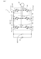
- FIG. 1 is a diagram showing an internal structure of the power conversion device of the first embodiment.
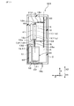
- FIG. 2 is a view of FIG. 1 as viewed from the arrangement direction of the semiconductor modules.
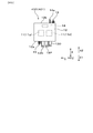
- FIG. 3 is an inverter circuit diagram of the power conversion device of the first embodiment.
- FIG. 4 is a plan view of the semiconductor module of the power conversion device of the second embodiment.
- FIG. 5 is a plan view of the semiconductor module of the power conversion device of the third embodiment.
- FIG. 6 is a diagram corresponding to FIG. 1 for the power conversion device of the fourth embodiment.
- FIG. 7 is a view of FIG. 6 as viewed from the arrangement direction of the semiconductor modules.
- FIG. 8 is a plan view of the semiconductor module of the power conversion device of the fifth embodiment.
- This power conversion device is mounted on a vehicle such as an electric vehicle or a hybrid vehicle, and is configured as an in-vehicle power conversion device that converts power between DC power and AC power.
- the first direction is indicated by an arrow X
- the second direction orthogonal to the first direction is indicated by an arrow Y
- a third direction orthogonal to both the first direction and the second direction is indicated.
- the direction is indicated by an arrow Z.
- the upper and lower sides of the power conversion device are not particularly limited, but in the following, for convenience of explanation, the upper side of FIG. 1 is the upper side of the power conversion device, and the lower side of FIG. 1 is the lower side of the power conversion device.
- the power conversion device 1 of the first embodiment includes three semiconductor modules 10, a capacitor module 20, a control circuit board 30 (see FIG. 2), and a cooler 40 (FIG. 2). 2), and these elements are housed in the internal space of the case 2.
- the case 2 it is preferable to adopt a resin case made of a resin material to reduce the weight.
- Each semiconductor module 10 has two semiconductor elements 11, a main body 12, a positive electrode terminal 13P, a negative electrode terminal 13N, an output terminal 13O, a current sensor element 14, and a control terminal 15.
- the semiconductor element 11 has a substantially flat plate shape with the third direction Z as the thickness direction.
- the semiconductor element 11 is also referred to as a "switching element” or a “semiconductor chip".
- any semiconductor element such as an IGBT (that is, an insulated gate bipolar transistor) and a MOSFET (that is, a MOS field effect transistor) is typically used.
- the lower semiconductor element 11 is the upper arm semiconductor element 11u
- the upper semiconductor element 11 is the lower arm semiconductor element 11d.
- the main body 12 is mainly composed of a resin material, and is configured to incorporate two semiconductor elements 11 (upper arm semiconductor element 11u and lower arm semiconductor element 11d) and a current sensor element 14. ..
- the main body 12 has a substantially rectangular parallelepiped shape with the third direction Z as the thickness direction.
- the upper arm semiconductor element 11u and the lower arm semiconductor element 11d are juxtaposed in the first direction X adjacent to each other.
- the positive electrode terminal 13P is a metal terminal for electrically connecting the semiconductor element 11 to the positive electrode side of the power source (see “power source B” in FIG. 3) described later, and the negative electrode terminal 13N is the semiconductor element 11 Is a metal terminal for electrically connecting to the negative electrode side of this power supply.
- the positive electrode terminal 13P is electrically connected to the metal positive electrode bus bar 16 on the capacitor module 20 side, and the negative electrode terminal 13N is electrically connected to the metal negative electrode bus bar 17 on the capacitor module 20 side.
- the positive electrode terminal 13P and the negative electrode terminal 13N have a flat plate shape with the second direction Y as the plate width direction and the third direction Z as the plate thickness direction, and are opposed to the lower side of the main body 12 facing the capacitor module 20. It projects linearly from the surface 12a toward the capacitor module 20 in the downward projecting direction X1. At this time, the positive electrode terminal 13P and the negative electrode terminal 13N are arranged in parallel with each other.
- the output terminal 13O is a metal terminal for electrically connecting the semiconductor element 11 to an electric power device (see “motor M" in FIG. 3).
- the output terminal 13O has a flat plate shape in which the second direction Y is the plate width direction and the third direction Z is the plate thickness direction, and projects from the upper surface 12b of the main body 12 in the upward projecting direction X2. That is, the output terminal 13O protrudes from the main body 12 in the direction opposite to that of the positive electrode terminal 13P and the negative electrode terminal 13N.
- the current sensor element 14 constitutes a current sensor that detects the current flowing through the semiconductor element 11, and the sensor terminal 14a is configured to be electrically connected to the metal output bus bar 18.
- the current sensor element 14 is provided on the side opposite to the upper arm semiconductor element 11u with the lower arm semiconductor element 11d sandwiched in the first direction X, and is the output terminal 13O and the control terminal 15 of the upper surface 12b of the main body 12. It protrudes in the protruding direction X2 from the portion between and. Therefore, the current sensor element 14 is linearly arranged in the first direction X with respect to the two semiconductor elements 11.
- the current sensor including the current sensor element 14
- various current sensors using known detection methods can be used.
- the current sensor may be of a detection type including a magnetic collection core, or may be of a detection type without a magnetic collection core.
- the control terminal 15 is a metal terminal provided for each of the two semiconductor elements 11.
- the control terminal 15 of one of the semiconductor elements 11 projects in the projecting direction X1 from the facing surface 12a of the main body 12.
- the control terminal 15 of the other semiconductor element 11 projects from the upper surface 12b of the main body 12 in the projecting direction X2, which is opposite to the projecting direction X1.
- the capacitor module 20 is electrically connected to the three semiconductor modules 10.
- the capacitor module 20 has a capacitor element 21 of a smoothing capacitor and a resin capacitor case 22 for accommodating the capacitor element 21, and the capacitor element 21 is housed in the capacitor case 22 and hardened with a potting resin. There is.
- the three semiconductor modules 10 are arranged with the second direction Y orthogonal to the protruding direction X1 as the arrangement direction.
- the main body 12 of each semiconductor module 10 is viewed from the third direction (orthogonal direction) Z orthogonal to both the protruding direction X1 and the second direction (arrangement direction) Y, each semiconductor element 11 and the current sensor are viewed in the main body 12.
- the elements 14 are arranged so as not to overlap each other.
- the third direction Z coincides with the normal direction of the surface 12c of the main body portion 12.
- the semiconductor modules 10 arranged on one end side in the second direction Y are designated as the first semiconductor module 10A, and the semiconductor modules 10 arranged on the other end side are designated as the first semiconductor module 10A.
- the semiconductor modules 10 arranged on the other end side are designated as the first semiconductor module 10A.
- the second semiconductor module 10B Let it be the second semiconductor module 10B.
- the positive electrode terminal 13P and the negative electrode terminal 13N of the first semiconductor module 10A the positive electrode terminal 13P located outside the second direction Y is referred to as the first electrode terminal 13A. Further, of the positive electrode terminal 13P and the negative electrode terminal 13N of the second semiconductor module 10B, the negative electrode terminal 13N located outside the second direction Y is referred to as the second electrode terminal 13B. At this time, the terminal separation distance D between the first electrode terminal 13A and the second electrode terminal 13B is smaller than the capacitor dimension L in the second direction Y of the capacitor module 20.
- the terminal separation distance D corresponds to the distance between the right end surface of the first electrode terminal 13A in the second direction Y and the left end surface of the second electrode terminal 13B in the second direction Y in FIG.
- the capacitor size L corresponds to the size of the capacitor case 22 in the second direction Y.
- the control circuit board is on the back surface 12d side of the main body 12. 30 are arranged.
- the control circuit board 30 is electrically connected to each of the control terminal 15 of each semiconductor module 10 and the sensor terminal 14a of the current sensor element 14, and has a function of performing switching control of each semiconductor element 11.
- the control circuit board 30 is arranged along the virtual plane A with the third direction Z as the thickness direction.
- the virtual plane A is a plane that faces parallel to the back surface 12d of the main body 12 with the third direction Z as the normal direction.
- This virtual plane A can be defined by the protruding direction X1 and the second direction Y.
- the control circuit board 30 is arranged so as to overlap the semiconductor element 11 and the current sensor element 14 in the third direction Z.
- the surface 12c of the main body 12 of each semiconductor module 10 is used as a surface to be cooled, and a cooler 40 that comes into contact with the surface to be cooled is provided.
- the cooler 40 has a function of cooling the three semiconductor modules 10 by using a cooling medium (hereinafter, simply referred to as “refrigerant”).
- the structure of the cooler 40 is not particularly limited, but as an example, the refrigerant flow path 41 is provided in the metal housing so as to overlap the semiconductor element 11 and the current sensor element 14 in the third direction Z. The dimensions are set to. As a result, the semiconductor element 11 and the current sensor element 14 are cooled by exchanging heat with the refrigerant flowing through the refrigerant flow path 41 of the cooler 40.
- Typical refrigerants used in the cooler 40 include water mixed with ethylene glycol-based antifreeze, natural refrigerants such as water and ammonia, fluorocarbon-based refrigerants such as Florinate, fluorocarbon refrigerants such as HCFC123 and HFC134a, and methanol. , Alcohol-based refrigerants such as alcohol, ketone-based refrigerants such as acetone, and the like can be adopted.
- the inverter circuit of the power conversion device 1 includes three-phase (U-phase, V-phase, W-phase) legs connected in parallel between the positive electrode side and the negative electrode side of the power supply B.
- the two semiconductor elements 11 built in the main body 12 are composed of an upper arm semiconductor element 11u and a lower arm semiconductor element 11d connected in series with each other.
- the upper arm semiconductor element 11u is electrically connected to the high potential side terminal of the power supply B.
- the lower arm semiconductor element 11d is electrically connected to the low potential side terminal of the power supply B.
- the connection points between the upper arm semiconductor element 11u and the lower arm semiconductor element 11d are connected to three electrodes of the motor M as an electric power device via an output bus bar 18 and a three-phase connector (not shown). Further, a flywheel diode is connected in antiparallel to each semiconductor element 11.
- each semiconductor module 10 having the semiconductor element 11 is electrically connected to the capacitor module 20.
- the main body 12 of each semiconductor module 10 has a built-in current sensor element 14 for detecting the current flowing through the semiconductor element 11 together with the semiconductor element 11.
- the semiconductor element 11 and the current sensor element 14 are preliminarily incorporated in the main body 12 of the semiconductor module 10. Therefore, it is possible to prevent the position shift of the current sensor with respect to the semiconductor module 10 that occurs when the current sensor incorporating the current sensor element 14 and the semiconductor module 10 are integrated by resin molding.
- both the positive electrode terminal 13P and the negative electrode terminal 11N project from the facing surface 12a of the main body 12 of each semiconductor module 10 toward the capacitor module 20 in the same protruding direction X1. Therefore, the positive electrode terminal 13P and the negative electrode terminal 13N of each semiconductor module 10 can be connected at a position close to the capacitor module 20 in the protruding direction X1, which simplifies the assembling work of each semiconductor module 10 and causes an assembly failure. Can be prevented.
- the power conversion device 1 capable of improving the manufacturing yield.
- the power conversion device 1 by connecting the positive electrode terminal 13P and the negative electrode terminal 13N of each semiconductor module 10 at a position close to the capacitor module 20, the circuit inductance is reduced and a high surge occurs during the switching operation of the semiconductor element 11. It is possible to prevent the generation of voltage. Further, since the semiconductor modules 10 are electrically connected to each other via the capacitor module 20, it is possible to suppress the influence of noise from one semiconductor module 10 to another semiconductor module 10.
- the semiconductor element 11 and the current sensor element 14 are formed by cooling the surface 12c of the main body 12 whose normal direction is the third direction Z in each semiconductor module 10 with the cooler 40. Each of them can be cooled independently, and the degree of freedom of cooling of each semiconductor module 10 can be improved.
- the three semiconductor modules 10 are arranged within the range of the size of the capacitor module 20 in the second direction Y. Becomes possible. This is effective in reducing the size of the physique of the power conversion device 1.
- the control circuit board 30 is arranged parallel to the back surface 12d of the main body 12 of each semiconductor module 10 and overlaps with each semiconductor element 11 and the current sensor element 14 in the third direction Z.
- the electrical connection distance between the control circuit board 30 and each of the semiconductor element 11 and the current sensor element 14 can be suppressed to be short. As a result, it is possible to prevent a control delay of the semiconductor element 11 and improve the detection accuracy of the current sensor element 14.
- a structure is adopted in which a refrigerant flow path through which the refrigerant flows is formed by using a part of the case 2 in place of or in addition to the cooler 40 for cooling each semiconductor module 10. You can also do it.
- each semiconductor module 110 is configured such that two semiconductor elements 11 built in the main body 12 are juxtaposed in the second direction Y.
- the dimension of the first direction X of each semiconductor module 110 can be suppressed to be smaller than that of the first embodiment.
- each semiconductor module 210 is different from that of the first embodiment.
- each semiconductor module 210 is configured such that the output terminal 13O projects from one side surface of the second direction Y of the main body 12.
- the power conversion device 201 of the third embodiment by changing the protruding position of the output terminal 13O, the dimension of the first direction X of each semiconductor module 210 can be suppressed to be smaller than that of the first embodiment.
- the power conversion device 301 of the fourth embodiment is different from that of the first embodiment in the configuration of each semiconductor module 310 and the peripheral structure of the capacitor module 20.
- each semiconductor module 310 is configured such that the output terminal 13O projects in the projecting direction X1 from the lower facing surface 12a of the main body 12 facing the capacitor module 20. That is, the output terminal 13O protrudes from the main body 12 in the same protruding direction X1 as the positive electrode terminal 13P and the negative electrode terminal 11N.
- the output bus bar 18 electrically connected to the output terminal 13O has a capacitor module and 20 between one end 18a and the other end 18b, which are connection portions with the output terminal 13O. It extends to avoid interference.
- the output bus bar 18 is configured so that a part thereof is inserted into the case 2 made of resin. At this time, in order to reduce the circuit inductance, it is preferable to keep the energization path formed by the output bus bar 18 shorter.
- the power conversion device 301 includes a cooler 50 as a cooling unit for cooling the condenser module 20.
- the cooler 50 is provided between the capacitor module 20 and the output bus bar 18, particularly between the capacitor module 20 and the output bus bar 18 which is inserted into the case 2.
- the structure of the cooler 50 is not particularly limited, but as an example, like the above-mentioned cooler 40, a cooler 50 having a refrigerant flow path 51 in which the refrigerant flows in parallel is used in the metal housing. be able to. If necessary, the cooler 50 can also be applied to the power conversion device 1 of the first embodiment.
- the cooler 50 may be arranged with a gap from the condenser case 22, or may be in contact with the condenser case 22 in order to improve the cooling performance of the condenser element 21. Further, the cooler 50 may be arranged with a gap from the insert portion of the output bus bar 18 in the case 2, or is in contact with the insert portion in order to improve the cooling performance of the output bus bar 18. You may.
- the condenser element 21 of the condenser module 20 is cooled by exchanging heat with the refrigerant flowing through the refrigerant flow path 51 of the cooler 50. At this time, the cooler 50 can also cool the output bus bar 18.
- the output terminal 13O is changed so as to project from the facing surface 12a of the main body 12 in the same protruding direction X1 as the positive electrode terminal 13P and the negative electrode terminal 11N, as compared with the first embodiment. Therefore, the dimension of each semiconductor module 310 in the first direction X can be kept small. In this case, the space on the upper surface 12b side of the main body 12 can be saved.
- a part of the case 2 is used to provide a refrigerant flow path through which the refrigerant flows.
- the formed structure can also be adopted.
- a cooler may be provided so as to cool the capacitor module 20 from both sides of the third direction Z.
- each semiconductor module 410 is different from that of the fourth embodiment.
- each semiconductor module 410 is configured such that two semiconductor elements 11 built in the main body 12 are juxtaposed in the second direction Y.
- the power conversion device 401 of the fifth embodiment by changing the arrangement of the two semiconductor elements 11, the dimension of the first direction X of each semiconductor module 410 can be suppressed to be smaller than that of the fourth embodiment.
- the case where the two semiconductor elements 11 are built in the main body 12 of each of the three semiconductor modules 10, 110, 210, 310, 410 has been illustrated, but the semiconductor modules 10, 110, 210, 310 have been illustrated.
- 410 and the number of semiconductor elements 11 are not limited to this, and can be appropriately changed as needed.
- the number of semiconductor elements 11 built in the main body 12 of each semiconductor module may be one.
- each semiconductor element 11 and the current sensor elements 14 do not overlap each other in the main body 12 of each semiconductor module has been illustrated, but instead of this, each semiconductor element 11 and the current sensor element 14 It is also possible to adopt a modification example in which the two are arranged so as to overlap each other.
- the terminal separation distance D between the first electrode terminal 13A and the second electrode terminal 13B is smaller than the capacitor dimension L in the second direction Y of the capacitor module 20 has been illustrated, but instead of this, the terminal It is also possible to adopt a modified example of the structure in which the separation distance D substantially matches the capacitor dimension L, or a modified example of the structure in which the terminal separation distance D exceeds the capacitor dimension L.
- control circuit board 30 is arranged along the virtual plane A determined by the first direction X and the second direction Y has been illustrated, but the arrangement of the control circuit board 30 is limited to this. Instead, the placement can be changed as needed.
Landscapes
- Engineering & Computer Science (AREA)
- Power Engineering (AREA)
- Inverter Devices (AREA)
Applications Claiming Priority (2)
| Application Number | Priority Date | Filing Date | Title |
|---|---|---|---|
| JP2019-198948 | 2019-10-31 | ||
| JP2019198948A JP2021072724A (ja) | 2019-10-31 | 2019-10-31 | 電力変換装置 |
Publications (1)
| Publication Number | Publication Date |
|---|---|
| WO2021084852A1 true WO2021084852A1 (ja) | 2021-05-06 |
Family
ID=75713840
Family Applications (1)
| Application Number | Title | Priority Date | Filing Date |
|---|---|---|---|
| PCT/JP2020/031257 Ceased WO2021084852A1 (ja) | 2019-10-31 | 2020-08-19 | 電力変換装置 |
Country Status (2)
| Country | Link |
|---|---|
| JP (1) | JP2021072724A (https=) |
| WO (1) | WO2021084852A1 (https=) |
Families Citing this family (1)
| Publication number | Priority date | Publication date | Assignee | Title |
|---|---|---|---|---|
| JP7278441B1 (ja) | 2022-02-15 | 2023-05-19 | 三菱電機株式会社 | 半導体モジュールおよび電力変換器 |
Citations (3)
| Publication number | Priority date | Publication date | Assignee | Title |
|---|---|---|---|---|
| JP2011198816A (ja) * | 2010-03-17 | 2011-10-06 | Keihin Corp | コンデンサ装置 |
| JP2014121121A (ja) * | 2012-12-13 | 2014-06-30 | Hitachi Automotive Systems Ltd | 電力変換装置 |
| JP2015115966A (ja) * | 2013-12-09 | 2015-06-22 | 三菱電機株式会社 | 電力変換装置付き回転電機 |
Family Cites Families (2)
| Publication number | Priority date | Publication date | Assignee | Title |
|---|---|---|---|---|
| JP4878520B2 (ja) * | 2006-08-09 | 2012-02-15 | 本田技研工業株式会社 | 半導体装置 |
| JP5738794B2 (ja) * | 2012-03-30 | 2015-06-24 | 日立オートモティブシステムズ株式会社 | 電力変換装置 |
-
2019
- 2019-10-31 JP JP2019198948A patent/JP2021072724A/ja active Pending
-
2020
- 2020-08-19 WO PCT/JP2020/031257 patent/WO2021084852A1/ja not_active Ceased
Patent Citations (3)
| Publication number | Priority date | Publication date | Assignee | Title |
|---|---|---|---|---|
| JP2011198816A (ja) * | 2010-03-17 | 2011-10-06 | Keihin Corp | コンデンサ装置 |
| JP2014121121A (ja) * | 2012-12-13 | 2014-06-30 | Hitachi Automotive Systems Ltd | 電力変換装置 |
| JP2015115966A (ja) * | 2013-12-09 | 2015-06-22 | 三菱電機株式会社 | 電力変換装置付き回転電機 |
Also Published As
| Publication number | Publication date |
|---|---|
| JP2021072724A (ja) | 2021-05-06 |
Similar Documents
| Publication | Publication Date | Title |
|---|---|---|
| CN101064485B (zh) | 电路装置、电路模块和电力变换装置和车载电机系统 | |
| JP4452953B2 (ja) | 電力変換装置 | |
| CN103081326B (zh) | 逆变器装置 | |
| JP4988665B2 (ja) | 半導体装置および半導体装置を用いた電力変換装置 | |
| CN104506050B (zh) | 电力转换装置 | |
| US8958225B2 (en) | Electric power converter | |
| CN103081331B (zh) | 逆变器装置 | |
| CN110247538B (zh) | 电力转换装置 | |
| US11424689B2 (en) | Power conversion device | |
| US10374523B2 (en) | Power conversion device | |
| US12095353B2 (en) | Capacitor module and power conversion device | |
| WO2012014842A1 (ja) | 電力変換装置 | |
| US11139752B2 (en) | Power conversion device with wiring having different parasitic inductances | |
| JP5250442B2 (ja) | 電力変換装置 | |
| JP2010182898A (ja) | コンデンサモジュール及びそれを用いた電力変換装置 | |
| CN118077131A (zh) | 电力转换装置 | |
| WO2021084852A1 (ja) | 電力変換装置 | |
| JP7632011B2 (ja) | パワーカード | |
| US20230328938A1 (en) | Power module | |
| US20230188000A1 (en) | Rotary electric machine unit | |
| JP2013099214A (ja) | インバータ装置 | |
| WO2025033118A1 (ja) | 半導体装置および電力変換装置 | |
| KR20150031633A (ko) | 차량용 인버터 |
Legal Events
| Date | Code | Title | Description |
|---|---|---|---|
| 121 | Ep: the epo has been informed by wipo that ep was designated in this application |
Ref document number: 20882025 Country of ref document: EP Kind code of ref document: A1 |
|
| NENP | Non-entry into the national phase |
Ref country code: DE |
|
| 122 | Ep: pct application non-entry in european phase |
Ref document number: 20882025 Country of ref document: EP Kind code of ref document: A1 |