WO2021084367A1 - 表示装置 - Google Patents
表示装置 Download PDFInfo
- Publication number
- WO2021084367A1 WO2021084367A1 PCT/IB2020/059794 IB2020059794W WO2021084367A1 WO 2021084367 A1 WO2021084367 A1 WO 2021084367A1 IB 2020059794 W IB2020059794 W IB 2020059794W WO 2021084367 A1 WO2021084367 A1 WO 2021084367A1
- Authority
- WO
- WIPO (PCT)
- Prior art keywords
- conductor
- insulator
- transistor
- display device
- layer
- Prior art date
- Legal status (The legal status is an assumption and is not a legal conclusion. Google has not performed a legal analysis and makes no representation as to the accuracy of the status listed.)
- Ceased
Links
Images

























Classifications
-
- G—PHYSICS
- G06—COMPUTING OR CALCULATING; COUNTING
- G06T—IMAGE DATA PROCESSING OR GENERATION, IN GENERAL
- G06T1/00—General purpose image data processing
- G06T1/20—Processor architectures; Processor configuration, e.g. pipelining
-
- G—PHYSICS
- G09—EDUCATION; CRYPTOGRAPHY; DISPLAY; ADVERTISING; SEALS
- G09G—ARRANGEMENTS OR CIRCUITS FOR CONTROL OF INDICATING DEVICES USING STATIC MEANS TO PRESENT VARIABLE INFORMATION
- G09G3/00—Control arrangements or circuits, of interest only in connection with visual indicators other than cathode-ray tubes
- G09G3/20—Control arrangements or circuits, of interest only in connection with visual indicators other than cathode-ray tubes for presentation of an assembly of a number of characters, e.g. a page, by composing the assembly by combination of individual elements arranged in a matrix no fixed position being assigned to or needed to be assigned to the individual characters or partial characters
- G09G3/22—Control arrangements or circuits, of interest only in connection with visual indicators other than cathode-ray tubes for presentation of an assembly of a number of characters, e.g. a page, by composing the assembly by combination of individual elements arranged in a matrix no fixed position being assigned to or needed to be assigned to the individual characters or partial characters using controlled light sources
- G09G3/30—Control arrangements or circuits, of interest only in connection with visual indicators other than cathode-ray tubes for presentation of an assembly of a number of characters, e.g. a page, by composing the assembly by combination of individual elements arranged in a matrix no fixed position being assigned to or needed to be assigned to the individual characters or partial characters using controlled light sources using electroluminescent panels
-
- G—PHYSICS
- G09—EDUCATION; CRYPTOGRAPHY; DISPLAY; ADVERTISING; SEALS
- G09G—ARRANGEMENTS OR CIRCUITS FOR CONTROL OF INDICATING DEVICES USING STATIC MEANS TO PRESENT VARIABLE INFORMATION
- G09G3/00—Control arrangements or circuits, of interest only in connection with visual indicators other than cathode-ray tubes
- G09G3/20—Control arrangements or circuits, of interest only in connection with visual indicators other than cathode-ray tubes for presentation of an assembly of a number of characters, e.g. a page, by composing the assembly by combination of individual elements arranged in a matrix no fixed position being assigned to or needed to be assigned to the individual characters or partial characters
- G09G3/22—Control arrangements or circuits, of interest only in connection with visual indicators other than cathode-ray tubes for presentation of an assembly of a number of characters, e.g. a page, by composing the assembly by combination of individual elements arranged in a matrix no fixed position being assigned to or needed to be assigned to the individual characters or partial characters using controlled light sources
- G09G3/30—Control arrangements or circuits, of interest only in connection with visual indicators other than cathode-ray tubes for presentation of an assembly of a number of characters, e.g. a page, by composing the assembly by combination of individual elements arranged in a matrix no fixed position being assigned to or needed to be assigned to the individual characters or partial characters using controlled light sources using electroluminescent panels
- G09G3/32—Control arrangements or circuits, of interest only in connection with visual indicators other than cathode-ray tubes for presentation of an assembly of a number of characters, e.g. a page, by composing the assembly by combination of individual elements arranged in a matrix no fixed position being assigned to or needed to be assigned to the individual characters or partial characters using controlled light sources using electroluminescent panels semiconductive, e.g. using light-emitting diodes [LED]
- G09G3/3208—Control arrangements or circuits, of interest only in connection with visual indicators other than cathode-ray tubes for presentation of an assembly of a number of characters, e.g. a page, by composing the assembly by combination of individual elements arranged in a matrix no fixed position being assigned to or needed to be assigned to the individual characters or partial characters using controlled light sources using electroluminescent panels semiconductive, e.g. using light-emitting diodes [LED] organic, e.g. using organic light-emitting diodes [OLED]
- G09G3/3275—Details of drivers for data electrodes
-
- G—PHYSICS
- G02—OPTICS
- G02F—OPTICAL DEVICES OR ARRANGEMENTS FOR THE CONTROL OF LIGHT BY MODIFICATION OF THE OPTICAL PROPERTIES OF THE MEDIA OF THE ELEMENTS INVOLVED THEREIN; NON-LINEAR OPTICS; FREQUENCY-CHANGING OF LIGHT; OPTICAL LOGIC ELEMENTS; OPTICAL ANALOGUE/DIGITAL CONVERTERS
- G02F1/00—Devices or arrangements for the control of the intensity, colour, phase, polarisation or direction of light arriving from an independent light source, e.g. switching, gating or modulating; Non-linear optics
- G02F1/01—Devices or arrangements for the control of the intensity, colour, phase, polarisation or direction of light arriving from an independent light source, e.g. switching, gating or modulating; Non-linear optics for the control of the intensity, phase, polarisation or colour
- G02F1/13—Devices or arrangements for the control of the intensity, colour, phase, polarisation or direction of light arriving from an independent light source, e.g. switching, gating or modulating; Non-linear optics for the control of the intensity, phase, polarisation or colour based on liquid crystals, e.g. single liquid crystal display cells
- G02F1/133—Constructional arrangements; Operation of liquid crystal cells; Circuit arrangements
-
- G—PHYSICS
- G02—OPTICS
- G02F—OPTICAL DEVICES OR ARRANGEMENTS FOR THE CONTROL OF LIGHT BY MODIFICATION OF THE OPTICAL PROPERTIES OF THE MEDIA OF THE ELEMENTS INVOLVED THEREIN; NON-LINEAR OPTICS; FREQUENCY-CHANGING OF LIGHT; OPTICAL LOGIC ELEMENTS; OPTICAL ANALOGUE/DIGITAL CONVERTERS
- G02F1/00—Devices or arrangements for the control of the intensity, colour, phase, polarisation or direction of light arriving from an independent light source, e.g. switching, gating or modulating; Non-linear optics
- G02F1/01—Devices or arrangements for the control of the intensity, colour, phase, polarisation or direction of light arriving from an independent light source, e.g. switching, gating or modulating; Non-linear optics for the control of the intensity, phase, polarisation or colour
- G02F1/13—Devices or arrangements for the control of the intensity, colour, phase, polarisation or direction of light arriving from an independent light source, e.g. switching, gating or modulating; Non-linear optics for the control of the intensity, phase, polarisation or colour based on liquid crystals, e.g. single liquid crystal display cells
- G02F1/133—Constructional arrangements; Operation of liquid crystal cells; Circuit arrangements
- G02F1/1333—Constructional arrangements; Manufacturing methods
- G02F1/1345—Conductors connecting electrodes to cell terminals
- G02F1/13454—Drivers integrated on the active matrix substrate
-
- G—PHYSICS
- G02—OPTICS
- G02F—OPTICAL DEVICES OR ARRANGEMENTS FOR THE CONTROL OF LIGHT BY MODIFICATION OF THE OPTICAL PROPERTIES OF THE MEDIA OF THE ELEMENTS INVOLVED THEREIN; NON-LINEAR OPTICS; FREQUENCY-CHANGING OF LIGHT; OPTICAL LOGIC ELEMENTS; OPTICAL ANALOGUE/DIGITAL CONVERTERS
- G02F1/00—Devices or arrangements for the control of the intensity, colour, phase, polarisation or direction of light arriving from an independent light source, e.g. switching, gating or modulating; Non-linear optics
- G02F1/01—Devices or arrangements for the control of the intensity, colour, phase, polarisation or direction of light arriving from an independent light source, e.g. switching, gating or modulating; Non-linear optics for the control of the intensity, phase, polarisation or colour
- G02F1/13—Devices or arrangements for the control of the intensity, colour, phase, polarisation or direction of light arriving from an independent light source, e.g. switching, gating or modulating; Non-linear optics for the control of the intensity, phase, polarisation or colour based on liquid crystals, e.g. single liquid crystal display cells
- G02F1/133—Constructional arrangements; Operation of liquid crystal cells; Circuit arrangements
- G02F1/136—Liquid crystal cells structurally associated with a semi-conducting layer or substrate, e.g. cells forming part of an integrated circuit
- G02F1/1362—Active matrix addressed cells
-
- G—PHYSICS
- G02—OPTICS
- G02F—OPTICAL DEVICES OR ARRANGEMENTS FOR THE CONTROL OF LIGHT BY MODIFICATION OF THE OPTICAL PROPERTIES OF THE MEDIA OF THE ELEMENTS INVOLVED THEREIN; NON-LINEAR OPTICS; FREQUENCY-CHANGING OF LIGHT; OPTICAL LOGIC ELEMENTS; OPTICAL ANALOGUE/DIGITAL CONVERTERS
- G02F1/00—Devices or arrangements for the control of the intensity, colour, phase, polarisation or direction of light arriving from an independent light source, e.g. switching, gating or modulating; Non-linear optics
- G02F1/01—Devices or arrangements for the control of the intensity, colour, phase, polarisation or direction of light arriving from an independent light source, e.g. switching, gating or modulating; Non-linear optics for the control of the intensity, phase, polarisation or colour
- G02F1/13—Devices or arrangements for the control of the intensity, colour, phase, polarisation or direction of light arriving from an independent light source, e.g. switching, gating or modulating; Non-linear optics for the control of the intensity, phase, polarisation or colour based on liquid crystals, e.g. single liquid crystal display cells
- G02F1/133—Constructional arrangements; Operation of liquid crystal cells; Circuit arrangements
- G02F1/136—Liquid crystal cells structurally associated with a semi-conducting layer or substrate, e.g. cells forming part of an integrated circuit
- G02F1/1362—Active matrix addressed cells
- G02F1/136277—Active matrix addressed cells formed on a semiconductor substrate, e.g. of silicon
-
- G—PHYSICS
- G02—OPTICS
- G02F—OPTICAL DEVICES OR ARRANGEMENTS FOR THE CONTROL OF LIGHT BY MODIFICATION OF THE OPTICAL PROPERTIES OF THE MEDIA OF THE ELEMENTS INVOLVED THEREIN; NON-LINEAR OPTICS; FREQUENCY-CHANGING OF LIGHT; OPTICAL LOGIC ELEMENTS; OPTICAL ANALOGUE/DIGITAL CONVERTERS
- G02F1/00—Devices or arrangements for the control of the intensity, colour, phase, polarisation or direction of light arriving from an independent light source, e.g. switching, gating or modulating; Non-linear optics
- G02F1/01—Devices or arrangements for the control of the intensity, colour, phase, polarisation or direction of light arriving from an independent light source, e.g. switching, gating or modulating; Non-linear optics for the control of the intensity, phase, polarisation or colour
- G02F1/13—Devices or arrangements for the control of the intensity, colour, phase, polarisation or direction of light arriving from an independent light source, e.g. switching, gating or modulating; Non-linear optics for the control of the intensity, phase, polarisation or colour based on liquid crystals, e.g. single liquid crystal display cells
- G02F1/133—Constructional arrangements; Operation of liquid crystal cells; Circuit arrangements
- G02F1/136—Liquid crystal cells structurally associated with a semi-conducting layer or substrate, e.g. cells forming part of an integrated circuit
- G02F1/1362—Active matrix addressed cells
- G02F1/136286—Wiring, e.g. gate line, drain line
-
- G—PHYSICS
- G02—OPTICS
- G02F—OPTICAL DEVICES OR ARRANGEMENTS FOR THE CONTROL OF LIGHT BY MODIFICATION OF THE OPTICAL PROPERTIES OF THE MEDIA OF THE ELEMENTS INVOLVED THEREIN; NON-LINEAR OPTICS; FREQUENCY-CHANGING OF LIGHT; OPTICAL LOGIC ELEMENTS; OPTICAL ANALOGUE/DIGITAL CONVERTERS
- G02F1/00—Devices or arrangements for the control of the intensity, colour, phase, polarisation or direction of light arriving from an independent light source, e.g. switching, gating or modulating; Non-linear optics
- G02F1/01—Devices or arrangements for the control of the intensity, colour, phase, polarisation or direction of light arriving from an independent light source, e.g. switching, gating or modulating; Non-linear optics for the control of the intensity, phase, polarisation or colour
- G02F1/13—Devices or arrangements for the control of the intensity, colour, phase, polarisation or direction of light arriving from an independent light source, e.g. switching, gating or modulating; Non-linear optics for the control of the intensity, phase, polarisation or colour based on liquid crystals, e.g. single liquid crystal display cells
- G02F1/133—Constructional arrangements; Operation of liquid crystal cells; Circuit arrangements
- G02F1/136—Liquid crystal cells structurally associated with a semi-conducting layer or substrate, e.g. cells forming part of an integrated circuit
- G02F1/1362—Active matrix addressed cells
- G02F1/1368—Active matrix addressed cells in which the switching element is a three-electrode device
-
- G—PHYSICS
- G06—COMPUTING OR CALCULATING; COUNTING
- G06T—IMAGE DATA PROCESSING OR GENERATION, IN GENERAL
- G06T3/00—Geometric image transformations in the plane of the image
- G06T3/40—Scaling of whole images or parts thereof, e.g. expanding or contracting
- G06T3/4046—Scaling of whole images or parts thereof, e.g. expanding or contracting using neural networks
-
- G—PHYSICS
- G09—EDUCATION; CRYPTOGRAPHY; DISPLAY; ADVERTISING; SEALS
- G09F—DISPLAYING; ADVERTISING; SIGNS; LABELS OR NAME-PLATES; SEALS
- G09F9/00—Indicating arrangements for variable information in which the information is built-up on a support by selection or combination of individual elements
- G09F9/30—Indicating arrangements for variable information in which the information is built-up on a support by selection or combination of individual elements in which the desired character or characters are formed by combining individual elements
-
- G—PHYSICS
- G09—EDUCATION; CRYPTOGRAPHY; DISPLAY; ADVERTISING; SEALS
- G09G—ARRANGEMENTS OR CIRCUITS FOR CONTROL OF INDICATING DEVICES USING STATIC MEANS TO PRESENT VARIABLE INFORMATION
- G09G3/00—Control arrangements or circuits, of interest only in connection with visual indicators other than cathode-ray tubes
- G09G3/20—Control arrangements or circuits, of interest only in connection with visual indicators other than cathode-ray tubes for presentation of an assembly of a number of characters, e.g. a page, by composing the assembly by combination of individual elements arranged in a matrix no fixed position being assigned to or needed to be assigned to the individual characters or partial characters
- G09G3/22—Control arrangements or circuits, of interest only in connection with visual indicators other than cathode-ray tubes for presentation of an assembly of a number of characters, e.g. a page, by composing the assembly by combination of individual elements arranged in a matrix no fixed position being assigned to or needed to be assigned to the individual characters or partial characters using controlled light sources
- G09G3/30—Control arrangements or circuits, of interest only in connection with visual indicators other than cathode-ray tubes for presentation of an assembly of a number of characters, e.g. a page, by composing the assembly by combination of individual elements arranged in a matrix no fixed position being assigned to or needed to be assigned to the individual characters or partial characters using controlled light sources using electroluminescent panels
- G09G3/32—Control arrangements or circuits, of interest only in connection with visual indicators other than cathode-ray tubes for presentation of an assembly of a number of characters, e.g. a page, by composing the assembly by combination of individual elements arranged in a matrix no fixed position being assigned to or needed to be assigned to the individual characters or partial characters using controlled light sources using electroluminescent panels semiconductive, e.g. using light-emitting diodes [LED]
-
- G—PHYSICS
- G09—EDUCATION; CRYPTOGRAPHY; DISPLAY; ADVERTISING; SEALS
- G09G—ARRANGEMENTS OR CIRCUITS FOR CONTROL OF INDICATING DEVICES USING STATIC MEANS TO PRESENT VARIABLE INFORMATION
- G09G3/00—Control arrangements or circuits, of interest only in connection with visual indicators other than cathode-ray tubes
- G09G3/20—Control arrangements or circuits, of interest only in connection with visual indicators other than cathode-ray tubes for presentation of an assembly of a number of characters, e.g. a page, by composing the assembly by combination of individual elements arranged in a matrix no fixed position being assigned to or needed to be assigned to the individual characters or partial characters
- G09G3/22—Control arrangements or circuits, of interest only in connection with visual indicators other than cathode-ray tubes for presentation of an assembly of a number of characters, e.g. a page, by composing the assembly by combination of individual elements arranged in a matrix no fixed position being assigned to or needed to be assigned to the individual characters or partial characters using controlled light sources
- G09G3/30—Control arrangements or circuits, of interest only in connection with visual indicators other than cathode-ray tubes for presentation of an assembly of a number of characters, e.g. a page, by composing the assembly by combination of individual elements arranged in a matrix no fixed position being assigned to or needed to be assigned to the individual characters or partial characters using controlled light sources using electroluminescent panels
- G09G3/32—Control arrangements or circuits, of interest only in connection with visual indicators other than cathode-ray tubes for presentation of an assembly of a number of characters, e.g. a page, by composing the assembly by combination of individual elements arranged in a matrix no fixed position being assigned to or needed to be assigned to the individual characters or partial characters using controlled light sources using electroluminescent panels semiconductive, e.g. using light-emitting diodes [LED]
- G09G3/3208—Control arrangements or circuits, of interest only in connection with visual indicators other than cathode-ray tubes for presentation of an assembly of a number of characters, e.g. a page, by composing the assembly by combination of individual elements arranged in a matrix no fixed position being assigned to or needed to be assigned to the individual characters or partial characters using controlled light sources using electroluminescent panels semiconductive, e.g. using light-emitting diodes [LED] organic, e.g. using organic light-emitting diodes [OLED]
- G09G3/3225—Control arrangements or circuits, of interest only in connection with visual indicators other than cathode-ray tubes for presentation of an assembly of a number of characters, e.g. a page, by composing the assembly by combination of individual elements arranged in a matrix no fixed position being assigned to or needed to be assigned to the individual characters or partial characters using controlled light sources using electroluminescent panels semiconductive, e.g. using light-emitting diodes [LED] organic, e.g. using organic light-emitting diodes [OLED] using an active matrix
-
- G—PHYSICS
- G09—EDUCATION; CRYPTOGRAPHY; DISPLAY; ADVERTISING; SEALS
- G09G—ARRANGEMENTS OR CIRCUITS FOR CONTROL OF INDICATING DEVICES USING STATIC MEANS TO PRESENT VARIABLE INFORMATION
- G09G3/00—Control arrangements or circuits, of interest only in connection with visual indicators other than cathode-ray tubes
- G09G3/20—Control arrangements or circuits, of interest only in connection with visual indicators other than cathode-ray tubes for presentation of an assembly of a number of characters, e.g. a page, by composing the assembly by combination of individual elements arranged in a matrix no fixed position being assigned to or needed to be assigned to the individual characters or partial characters
- G09G3/34—Control arrangements or circuits, of interest only in connection with visual indicators other than cathode-ray tubes for presentation of an assembly of a number of characters, e.g. a page, by composing the assembly by combination of individual elements arranged in a matrix no fixed position being assigned to or needed to be assigned to the individual characters or partial characters by control of light from an independent source
- G09G3/36—Control arrangements or circuits, of interest only in connection with visual indicators other than cathode-ray tubes for presentation of an assembly of a number of characters, e.g. a page, by composing the assembly by combination of individual elements arranged in a matrix no fixed position being assigned to or needed to be assigned to the individual characters or partial characters by control of light from an independent source using liquid crystals
- G09G3/3611—Control of matrices with row and column drivers
- G09G3/3648—Control of matrices with row and column drivers using an active matrix
-
- G—PHYSICS
- G09—EDUCATION; CRYPTOGRAPHY; DISPLAY; ADVERTISING; SEALS
- G09G—ARRANGEMENTS OR CIRCUITS FOR CONTROL OF INDICATING DEVICES USING STATIC MEANS TO PRESENT VARIABLE INFORMATION
- G09G3/00—Control arrangements or circuits, of interest only in connection with visual indicators other than cathode-ray tubes
- G09G3/20—Control arrangements or circuits, of interest only in connection with visual indicators other than cathode-ray tubes for presentation of an assembly of a number of characters, e.g. a page, by composing the assembly by combination of individual elements arranged in a matrix no fixed position being assigned to or needed to be assigned to the individual characters or partial characters
- G09G3/34—Control arrangements or circuits, of interest only in connection with visual indicators other than cathode-ray tubes for presentation of an assembly of a number of characters, e.g. a page, by composing the assembly by combination of individual elements arranged in a matrix no fixed position being assigned to or needed to be assigned to the individual characters or partial characters by control of light from an independent source
- G09G3/36—Control arrangements or circuits, of interest only in connection with visual indicators other than cathode-ray tubes for presentation of an assembly of a number of characters, e.g. a page, by composing the assembly by combination of individual elements arranged in a matrix no fixed position being assigned to or needed to be assigned to the individual characters or partial characters by control of light from an independent source using liquid crystals
- G09G3/3611—Control of matrices with row and column drivers
- G09G3/3685—Details of drivers for data electrodes
-
- G—PHYSICS
- G09—EDUCATION; CRYPTOGRAPHY; DISPLAY; ADVERTISING; SEALS
- G09G—ARRANGEMENTS OR CIRCUITS FOR CONTROL OF INDICATING DEVICES USING STATIC MEANS TO PRESENT VARIABLE INFORMATION
- G09G3/00—Control arrangements or circuits, of interest only in connection with visual indicators other than cathode-ray tubes
- G09G3/20—Control arrangements or circuits, of interest only in connection with visual indicators other than cathode-ray tubes for presentation of an assembly of a number of characters, e.g. a page, by composing the assembly by combination of individual elements arranged in a matrix no fixed position being assigned to or needed to be assigned to the individual characters or partial characters
- G09G3/34—Control arrangements or circuits, of interest only in connection with visual indicators other than cathode-ray tubes for presentation of an assembly of a number of characters, e.g. a page, by composing the assembly by combination of individual elements arranged in a matrix no fixed position being assigned to or needed to be assigned to the individual characters or partial characters by control of light from an independent source
- G09G3/36—Control arrangements or circuits, of interest only in connection with visual indicators other than cathode-ray tubes for presentation of an assembly of a number of characters, e.g. a page, by composing the assembly by combination of individual elements arranged in a matrix no fixed position being assigned to or needed to be assigned to the individual characters or partial characters by control of light from an independent source using liquid crystals
- G09G3/3611—Control of matrices with row and column drivers
- G09G3/3685—Details of drivers for data electrodes
- G09G3/3688—Details of drivers for data electrodes suitable for active matrices only
-
- H—ELECTRICITY
- H05—ELECTRIC TECHNIQUES NOT OTHERWISE PROVIDED FOR
- H05B—ELECTRIC HEATING; ELECTRIC LIGHT SOURCES NOT OTHERWISE PROVIDED FOR; CIRCUIT ARRANGEMENTS FOR ELECTRIC LIGHT SOURCES, IN GENERAL
- H05B33/00—Electroluminescent light sources
- H05B33/12—Light sources with substantially two-dimensional [2D] radiating surfaces
- H05B33/14—Light sources with substantially two-dimensional [2D] radiating surfaces characterised by the chemical or physical composition or the arrangement of the electroluminescent material, or by the simultaneous addition of the electroluminescent material in or onto the light source
-
- H—ELECTRICITY
- H10—SEMICONDUCTOR DEVICES; ELECTRIC SOLID-STATE DEVICES NOT OTHERWISE PROVIDED FOR
- H10D—INORGANIC ELECTRIC SEMICONDUCTOR DEVICES
- H10D30/00—Field-effect transistors [FET]
- H10D30/60—Insulated-gate field-effect transistors [IGFET]
- H10D30/67—Thin-film transistors [TFT]
-
- H—ELECTRICITY
- H10—SEMICONDUCTOR DEVICES; ELECTRIC SOLID-STATE DEVICES NOT OTHERWISE PROVIDED FOR
- H10D—INORGANIC ELECTRIC SEMICONDUCTOR DEVICES
- H10D30/00—Field-effect transistors [FET]
- H10D30/60—Insulated-gate field-effect transistors [IGFET]
- H10D30/67—Thin-film transistors [TFT]
- H10D30/674—Thin-film transistors [TFT] characterised by the active materials
- H10D30/6755—Oxide semiconductors, e.g. zinc oxide, copper aluminium oxide or cadmium stannate
-
- H—ELECTRICITY
- H10—SEMICONDUCTOR DEVICES; ELECTRIC SOLID-STATE DEVICES NOT OTHERWISE PROVIDED FOR
- H10K—ORGANIC ELECTRIC SOLID-STATE DEVICES
- H10K59/00—Integrated devices, or assemblies of multiple devices, comprising at least one organic light-emitting element covered by group H10K50/00
- H10K59/10—OLED displays
- H10K59/12—Active-matrix OLED [AMOLED] displays
- H10K59/121—Active-matrix OLED [AMOLED] displays characterised by the geometry or disposition of pixel elements
- H10K59/1213—Active-matrix OLED [AMOLED] displays characterised by the geometry or disposition of pixel elements the pixel elements being TFTs
-
- G—PHYSICS
- G09—EDUCATION; CRYPTOGRAPHY; DISPLAY; ADVERTISING; SEALS
- G09G—ARRANGEMENTS OR CIRCUITS FOR CONTROL OF INDICATING DEVICES USING STATIC MEANS TO PRESENT VARIABLE INFORMATION
- G09G2300/00—Aspects of the constitution of display devices
- G09G2300/02—Composition of display devices
- G09G2300/023—Display panel composed of stacked panels
-
- G—PHYSICS
- G09—EDUCATION; CRYPTOGRAPHY; DISPLAY; ADVERTISING; SEALS
- G09G—ARRANGEMENTS OR CIRCUITS FOR CONTROL OF INDICATING DEVICES USING STATIC MEANS TO PRESENT VARIABLE INFORMATION
- G09G2300/00—Aspects of the constitution of display devices
- G09G2300/04—Structural and physical details of display devices
- G09G2300/0421—Structural details of the set of electrodes
- G09G2300/0426—Layout of electrodes and connections
-
- G—PHYSICS
- G09—EDUCATION; CRYPTOGRAPHY; DISPLAY; ADVERTISING; SEALS
- G09G—ARRANGEMENTS OR CIRCUITS FOR CONTROL OF INDICATING DEVICES USING STATIC MEANS TO PRESENT VARIABLE INFORMATION
- G09G2300/00—Aspects of the constitution of display devices
- G09G2300/08—Active matrix structure, i.e. with use of active elements, inclusive of non-linear two terminal elements, in the pixels together with light emitting or modulating elements
- G09G2300/0809—Several active elements per pixel in active matrix panels
- G09G2300/0842—Several active elements per pixel in active matrix panels forming a memory circuit, e.g. a dynamic memory with one capacitor
-
- G—PHYSICS
- G09—EDUCATION; CRYPTOGRAPHY; DISPLAY; ADVERTISING; SEALS
- G09G—ARRANGEMENTS OR CIRCUITS FOR CONTROL OF INDICATING DEVICES USING STATIC MEANS TO PRESENT VARIABLE INFORMATION
- G09G2340/00—Aspects of display data processing
- G09G2340/04—Changes in size, position or resolution of an image
- G09G2340/0407—Resolution change, inclusive of the use of different resolutions for different screen areas
-
- G—PHYSICS
- G09—EDUCATION; CRYPTOGRAPHY; DISPLAY; ADVERTISING; SEALS
- G09G—ARRANGEMENTS OR CIRCUITS FOR CONTROL OF INDICATING DEVICES USING STATIC MEANS TO PRESENT VARIABLE INFORMATION
- G09G3/00—Control arrangements or circuits, of interest only in connection with visual indicators other than cathode-ray tubes
- G09G3/20—Control arrangements or circuits, of interest only in connection with visual indicators other than cathode-ray tubes for presentation of an assembly of a number of characters, e.g. a page, by composing the assembly by combination of individual elements arranged in a matrix no fixed position being assigned to or needed to be assigned to the individual characters or partial characters
-
- G—PHYSICS
- G09—EDUCATION; CRYPTOGRAPHY; DISPLAY; ADVERTISING; SEALS
- G09G—ARRANGEMENTS OR CIRCUITS FOR CONTROL OF INDICATING DEVICES USING STATIC MEANS TO PRESENT VARIABLE INFORMATION
- G09G3/00—Control arrangements or circuits, of interest only in connection with visual indicators other than cathode-ray tubes
- G09G3/20—Control arrangements or circuits, of interest only in connection with visual indicators other than cathode-ray tubes for presentation of an assembly of a number of characters, e.g. a page, by composing the assembly by combination of individual elements arranged in a matrix no fixed position being assigned to or needed to be assigned to the individual characters or partial characters
- G09G3/22—Control arrangements or circuits, of interest only in connection with visual indicators other than cathode-ray tubes for presentation of an assembly of a number of characters, e.g. a page, by composing the assembly by combination of individual elements arranged in a matrix no fixed position being assigned to or needed to be assigned to the individual characters or partial characters using controlled light sources
- G09G3/30—Control arrangements or circuits, of interest only in connection with visual indicators other than cathode-ray tubes for presentation of an assembly of a number of characters, e.g. a page, by composing the assembly by combination of individual elements arranged in a matrix no fixed position being assigned to or needed to be assigned to the individual characters or partial characters using controlled light sources using electroluminescent panels
- G09G3/32—Control arrangements or circuits, of interest only in connection with visual indicators other than cathode-ray tubes for presentation of an assembly of a number of characters, e.g. a page, by composing the assembly by combination of individual elements arranged in a matrix no fixed position being assigned to or needed to be assigned to the individual characters or partial characters using controlled light sources using electroluminescent panels semiconductive, e.g. using light-emitting diodes [LED]
- G09G3/3208—Control arrangements or circuits, of interest only in connection with visual indicators other than cathode-ray tubes for presentation of an assembly of a number of characters, e.g. a page, by composing the assembly by combination of individual elements arranged in a matrix no fixed position being assigned to or needed to be assigned to the individual characters or partial characters using controlled light sources using electroluminescent panels semiconductive, e.g. using light-emitting diodes [LED] organic, e.g. using organic light-emitting diodes [OLED]
- G09G3/3225—Control arrangements or circuits, of interest only in connection with visual indicators other than cathode-ray tubes for presentation of an assembly of a number of characters, e.g. a page, by composing the assembly by combination of individual elements arranged in a matrix no fixed position being assigned to or needed to be assigned to the individual characters or partial characters using controlled light sources using electroluminescent panels semiconductive, e.g. using light-emitting diodes [LED] organic, e.g. using organic light-emitting diodes [OLED] using an active matrix
- G09G3/3233—Control arrangements or circuits, of interest only in connection with visual indicators other than cathode-ray tubes for presentation of an assembly of a number of characters, e.g. a page, by composing the assembly by combination of individual elements arranged in a matrix no fixed position being assigned to or needed to be assigned to the individual characters or partial characters using controlled light sources using electroluminescent panels semiconductive, e.g. using light-emitting diodes [LED] organic, e.g. using organic light-emitting diodes [OLED] using an active matrix with pixel circuitry controlling the current through the light-emitting element
Definitions
- One aspect of the present invention relates to a display device.
- One aspect of the present invention is not limited to the above technical fields.
- the technical fields of one aspect of the present invention disclosed in the present specification and the like include semiconductor devices, display devices, light emitting devices, power storage devices, storage devices, electronic devices, lighting devices, input devices, input / output devices, and methods for driving them. , Or a method for producing them, can be given as an example.
- Semiconductor devices refer to all devices that can function by utilizing semiconductor characteristics.
- Wearable display devices and stationary display devices are becoming widespread as display devices for augmented reality (AR) or virtual reality (VR).
- Examples of the wearable type display device include a head-mounted display (HMD: Head Mounted Display), a glasses-type display device, and the like.
- Examples of the stationary display device include a head-up display (HUD: Head-Up Display) and the like.
- Patent Document 1 discloses an HMD that makes it easy to image the user's eye.
- the display device for AR or VR such as HMD is provided with pixels at a high density so that the pixels are not visually recognized by the user.
- the pixel density is preferably 1000 ppi or more, more preferably 3000 ppi or more, further preferably 5000 ppi or more, and further preferably 7000 ppi or more.
- the display device for AR or VR is provided with a large number of pixels to display a high-resolution image. For example, it is preferable to display an image having a resolution of 4K2K, 8K4K, or higher.
- One aspect of the present invention is to provide a display device capable of displaying a high-resolution image.
- one aspect of the present invention is to provide a display device capable of displaying a high-quality image.
- one aspect of the present invention is to provide a display device having a narrow frame.
- one aspect of the present invention is to provide a small display device.
- one aspect of the present invention is to provide a display device capable of storing a large amount of data.
- one aspect of the present invention is to provide a display device having low power consumption.
- one aspect of the present invention is to provide a display device that can be driven at high speed.
- one aspect of the present invention is to provide a low-priced display device.
- one aspect of the present invention is to provide a display device having a high degree of freedom in layout.
- one aspect of the present invention is to provide a display device capable of displaying a high-definition image.
- one aspect of the present invention is to provide a display device having a high pixel density.
- one aspect of the present invention is to provide a display device capable of displaying a highly realistic image.
- one aspect of the present invention is to provide a display device capable of displaying a high-luminance image.
- one aspect of the present invention is to provide a highly reliable display device.
- one aspect of the present invention is to provide a new display device.
- a first layer and a second layer are laminated and provided, and a data driver circuit and an arithmetic circuit are provided in the first layer, and a second layer is provided.
- a neural network is configured in the arithmetic circuit
- the data driver circuit has an area overlapping the display unit
- the arithmetic circuit has an area overlapping the storage circuit.
- the storage circuit has a function of holding the first image data
- the arithmetic circuit reads the first image data held in the storage circuit from the storage circuit and refers to the first image data.
- a first layer, a second layer, and a third layer are provided so as to be laminated on each other, and the first layer includes a data driver circuit and an arithmetic circuit.
- a storage circuit is provided in the second layer
- a display unit is provided in the third layer
- a neural network is configured in the arithmetic circuit, and the arithmetic circuit, the storage circuit, and the display are provided.
- the unit has a region that overlaps with each other, the storage circuit has a function of holding the first image data, and the arithmetic circuit reads the first image data held in the storage circuit from the storage circuit and reads the first image data.
- It is a display device having a function of generating a second image data and supplying it to a data driver circuit by performing arithmetic processing using a neural network on the image data of 1.
- the display unit is provided with the first transistor
- the storage circuit is provided with the second transistor
- the channel forming regions of the first and second transistors have a metal oxide. You may.
- the first layer, the second layer, and the third layer are provided so as to be laminated on each other, and the second layer is the first layer and the third layer. It is provided between the layers, the first layer is provided with a storage circuit, the second layer is provided with a substrate, a data driver circuit, an arithmetic circuit, and the data driver circuit is provided. , The arithmetic circuit is provided on the substrate, the display unit is provided on the third layer, the conductor is provided so as to penetrate the substrate, and the storage circuit and the arithmetic circuit are provided via the conductor.
- a neural network is configured in the arithmetic circuit, the storage circuit, the arithmetic circuit, and the display unit have regions that overlap each other, and the storage circuit has a function of holding the first image data. Then, the arithmetic circuit reads the first image data held in the storage circuit from the storage circuit, and performs arithmetic processing on the first image data using a neural network to obtain the second image data.
- a display device having a function of generating and supplying the data to the data driver circuit.
- the data driver circuit may have an area overlapping the display unit.
- the arithmetic circuit may have a function of generating the second image data by performing a process of increasing the resolution of the image represented by the first image data.
- a display device capable of displaying a high-resolution image.
- a display device capable of displaying a high-quality image.
- a display device having a narrow frame can be provided.
- a small display device can be provided.
- a display device having low power consumption can be provided.
- a display device that can be driven at high speed.
- one aspect of the present invention can provide a low-cost display device.
- a display device capable of displaying a high-luminance image.
- one aspect of the present invention can provide a highly reliable display device.
- a novel display device can be provided by one aspect of the present invention.
- FIG. 1 is a block diagram showing a configuration example of a display device.
- FIG. 2 is a block diagram showing a configuration example of the display device.
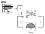
- 3A and 3B are diagrams showing an example of arithmetic processing.
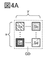
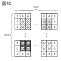
- 4A to 4C are diagrams showing an example of arithmetic processing.
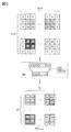
- FIG. 5 is a diagram showing an example of arithmetic processing.
- FIG. 6 is a block diagram showing a configuration example of the display device.
- FIG. 7 is a block diagram showing a configuration example of the display device.
- FIG. 8 is a block diagram showing a configuration example of the display device.
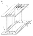
- FIG. 9 is a schematic diagram showing an example of arrangement of a gate driver circuit and a data driver circuit.
- FIG. 9 is a schematic diagram showing an example of arrangement of a gate driver circuit and a data driver circuit.
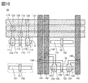
- FIG. 10 is a top view showing a configuration example of a gate driver circuit and a data driver circuit.
- FIG. 11 is a block diagram showing a configuration example of the display device.
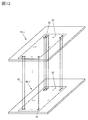
- FIG. 12 is a block diagram showing a configuration example of the display device.
- FIG. 13 is a block diagram showing a configuration example of the display device.
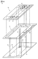
- FIG. 14 is a block diagram showing a configuration example of the display device.
- FIG. 15 is a block diagram showing a configuration example of the display device.
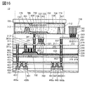
- FIG. 16 is a cross-sectional view showing a configuration example of the display device.
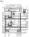
- FIG. 17 is a cross-sectional view showing a configuration example of the display device.
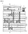
- FIG. 18 is a cross-sectional view showing a configuration example of the display device.
- FIG. 11 is a block diagram showing a configuration example of the display device.
- FIG. 12 is a block diagram showing a configuration example of the display device.
- FIG. 13 is a block diagram showing a configuration example of the display device
- FIG. 19 is a cross-sectional view showing a configuration example of the display device.
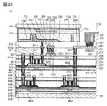
- FIG. 20 is a cross-sectional view showing a configuration example of the display device.
- FIG. 21 is a cross-sectional view showing a configuration example of the display device.
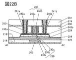
- FIG. 22A is a top view showing a configuration example of the transistor.
- 22B and 22C are cross-sectional views showing a configuration example of a transistor.
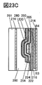
- FIG. 23A is a top view showing a configuration example of the transistor.
- 23B and 23C are cross-sectional views showing a configuration example of a transistor.
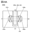
- FIG. 24A is a top view showing a configuration example of the transistor.
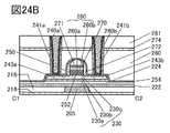
- 24B and 24C are cross-sectional views showing a configuration example of the transistor.
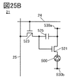
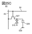
- FIG. 25A to 25C are circuit diagrams showing a configuration example of pixels.
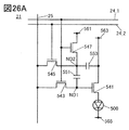
- FIG. 26A is a circuit diagram showing a configuration example of pixels.
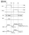
- FIG. 26B is a timing chart showing an example of a pixel driving method.
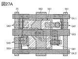
- FIG. 27A is a diagram showing an example of pixel layout.
- FIG. 27B is a circuit diagram showing a configuration example of pixels.
- FIG. 28 is a diagram showing an example of pixel layout.
- FIG. 29 is a schematic diagram showing a configuration example of pixels.
- 30A to 30C are circuit diagrams showing a configuration example of a cell.
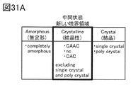
- FIG. 31A is a diagram illustrating the classification of the crystal structure of IGZO.
- FIG. 31B is a diagram illustrating an XRD spectrum of the CAAC-IGZO film.
- FIG. 31C is a diagram for explaining the microelectron diffraction pattern of the CAAC-IGZO film.
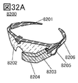
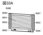
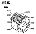
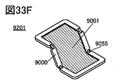
- 32A to 32D are perspective views showing an example of an electronic device.
- the source and drain functions of the transistor may be interchanged when the polarity of the transistor or the direction of the current changes in driving the circuit. Therefore, the terms source and drain can be interchanged.
- Electrodes do not functionally limit these components.
- an “electrode” may be used as part of a “wiring” and vice versa.
- the term “electrode” or “wiring” also includes a case where a plurality of “electrodes” or “wiring” are integrally formed.
- a “terminal” may be used as part of a “wiring” or “electrode” and vice versa.
- terminal includes a case where a plurality of "electrodes”, “wiring”, “terminals” and the like are integrally formed.
- the "electrode” can be a part of the “wiring” or the “terminal”, and for example, the “terminal” can be a part of the “wiring” or the “electrode”.
- terms such as “electrode”, “wiring”, and “terminal” may be replaced with terms such as "area” in some cases.
- the resistance value of "resistance” may be determined by the length of wiring.
- the resistance value may be determined by connecting to a conductor having a resistivity different from that of the conductor used in wiring.
- the resistance value may be determined by doping the semiconductor with impurities.
- electrically connected includes a case of being directly connected and a case of being connected via "something having some electrical action".
- the "thing having some kind of electrical action” is not particularly limited as long as it enables the exchange of electric signals between the connection targets. Therefore, even when it is expressed as “electrically connected”, in an actual circuit, there is a case where there is no physical connection part and only the wiring is extended. Further, even when expressed as "direct connection”, a case where different conductors are connected via a contact is included. In the wiring, there are cases where different conductors contain one or more same elements and cases where different conductors contain different elements.
- the voltage often indicates a potential difference between a certain potential and a reference potential (for example, a ground potential or a source potential). Therefore, it is often possible to paraphrase voltage and potential. In the present specification and the like, voltage and potential can be paraphrased unless otherwise specified.
- membrane and the term “layer” can be interchanged with each other.
- conductive layer and “insulating layer” may be interchangeable with the terms “conductive film” and “insulating film”.
- the off current means a drain current when the transistor is in an off state (also referred to as a non-conducting state or a cutoff state).
- the off state is a state in which the voltage V gs between the gate and the source is lower than the threshold voltage V th in the n-channel transistor (higher than V th in the p-channel transistor) unless otherwise specified. To say.
- the size, layer thickness, or area may be exaggerated for clarity. Therefore, it is not necessarily limited to that scale.
- the drawings schematically show ideal examples, and are not limited to the shapes or values shown in the drawings.
- a layer, a resist mask, or the like may be unintentionally reduced due to a treatment such as etching, but it may not be reflected in the drawing for easy understanding.
- the same reference numerals may be used in common between different drawings for the same parts or parts having the same functions / materials, and the repeated description thereof may be omitted.
- the hatch pattern may be the same and no particular sign may be added.
- One aspect of the present invention relates to a display device in which a first layer and a second layer are laminated.
- a data driver circuit and an arithmetic circuit are provided in the first layer, and a display unit is provided in the second layer. Pixels are arranged in a matrix on the display unit.
- the arithmetic circuit provided in the first layer has an area overlapping with the display unit provided in the second layer.
- the area of the display unit can be increased, so that many pixels can be provided in the display unit. Therefore, a high-resolution image can be displayed on the display unit. For example, an image having a resolution of 4K2K, 8K4K, or higher can be displayed on the display unit.
- the display device of one aspect of the present invention can be narrowed. Further, the display device according to one aspect of the present invention can be miniaturized.
- a neural network is configured in the arithmetic circuit, and for example, processing for increasing the resolution of the image represented by the image data input to the display device of one aspect of the present invention, that is, up-conversion can be performed. Since the arithmetic circuit has a function of up-converting, a high-resolution image can be displayed on the display unit even if the image resolution represented by the image data input to the display device of one aspect of the present invention is low. .. Therefore, the data capacity of the image data input to the display device of one aspect of the present invention can be reduced. Further, by performing the up-conversion using the neural network, the up-conversion can be performed with high accuracy, so that a high-quality image can be displayed on the display unit. From the above, since the arithmetic circuit has a function of up-converting image data using a neural network, the display device of one aspect of the present invention can display a high-resolution and high-quality image.
- FIG. 1 is a block diagram showing a configuration example of a display device 10 which is a display device according to an aspect of the present invention.
- the display device 10 has a display unit 20, in which pixels 21 are arranged in a matrix. Further, the display device 10 includes a gate driver circuit 22 and a data driver circuit 23. Further, the display device 10 includes a control circuit 31, a storage circuit 32, and an arithmetic circuit 33.
- the gate driver circuit 22 is electrically connected to the pixel 21 via the wiring 24.
- the pixels 21 in the same row can be electrically connected to the same wiring 24. It can be said that the wiring 24 that electrically connects the gate driver circuit 22 and the pixel 21 is a gate wire.
- the data driver circuit 23 is electrically connected to the pixel 21 via the wiring 25.
- the pixels 21 in the same row can be electrically connected to the same wiring 25. It can be said that the wiring 25 that electrically connects the data driver circuit 23 and the pixels 21 is a data line.
- the control circuit 31, the storage circuit 32, and the arithmetic circuit 33 are electrically connected to each other via a transmission line 34.
- the arithmetic circuit 33 is electrically connected to the data driver circuit 23.
- the image data GD can be supplied to the transmission line 34, and the image data GD is supplied to the storage circuit 32 via the transmission line 34.
- the control circuit 31 has a function of controlling the drive of the storage circuit 32 and the arithmetic circuit 33. Specifically, the control circuit 31 controls the drive of the storage circuit 32 and the calculation circuit 33 by generating a control signal and supplying the control signal to the storage circuit 32 and the calculation circuit 33 via the transmission line 34. Can be done.
- the control signal can be, for example, a clock signal.
- the control circuit 31 has a central processing unit (CPU: Central Processing Unit). Further, the control circuit 31 may have a microprocessor such as a DSP (Digital Signal Processor) or a GPU (Graphics Processing Unit). The microprocessor may have a configuration realized by a PLD (Programmable Logic Device) such as FPGA (Field Programmable Gate Array) or FPAA (Field Programmable Analog Array).
- CPU Central Processing Unit
- DSP Digital Signal Processor
- GPU Graphics Processing Unit
- the microprocessor may have a configuration realized by a PLD (Programmable Logic Device) such as FPGA (Field Programmable Gate Array) or FPAA (Field Programmable Analog Array).
- PLD Programmable Logic Device
- FPGA Field Programmable Gate Array
- FPAA Field Programmable Analog Array
- the storage circuit 32 has a function of holding the data supplied from the transmission line 34. Further, the storage circuit 32 has a function of outputting the held data to the transmission line 34. For example, the storage circuit 32 can hold the image data GD supplied to the storage circuit 32 via the transmission line 34. Further, the data held in the storage circuit 32 can be supplied to the arithmetic circuit 33 via the transmission line 34.
- the storage circuit 32 may have, for example, a DRAM (Dynamic Random Access Memory), a SRAM (Static Random Access Memory), or the like. Further, the storage circuit 32 can be configured to have a ROM (Read Only Memory). Examples of the ROM include a mask ROM, an OTPROM (One Time Program Read Only Memory), an EPROM (Erasable Program Read Only Memory), and the like. Examples of EPROM include UV-EPROM (Ultra-Violet Erasable Program Read Only Memory), EEPROM (Electrically Erasable Program Memory), etc., which enable erasure of stored data by irradiation with ultraviolet rays.
- ROM Read Only Memory
- Examples of the ROM include a mask ROM, an OTPROM (One Time Program Read Only Memory), an EPROM (Erasable Program Read Only Memory), and the like. Examples of EPROM include UV-EPROM (Ultra-Violet Erasable Program Read Only Memory), EEPROM (Electrically Erasable Program
- the arithmetic circuit 33 has a function of performing arithmetic processing on the image data GD. Specifically, it has a function of reading the image data GD held in the storage circuit 32 and performing arithmetic processing.
- the data acquired by the arithmetic circuit 33 in the process of arithmetic processing can be held in the storage circuit 32 and can be read out from the storage circuit 32 as needed.
- the image data for which the arithmetic processing has been completed can be output to the data driver circuit 23.
- a neural network NN is configured in the arithmetic circuit 33.
- the arithmetic circuit 33 can perform arithmetic operations using the neural network NN.
- learning can be performed using a server or the like provided outside the display device 10 and having a neural network similar to the neural network NN configured in the arithmetic circuit 33, and the learning result can be stored in the storage circuit 32. it can.
- the learning result can be, for example, a weighting coefficient.
- the neural network NN can make an inference to the image data GD. If the arithmetic performance of the arithmetic circuit 33 is sufficiently high, learning may be performed by the arithmetic circuit 33.
- a storage circuit may be incorporated in the arithmetic circuit 33.
- a storage circuit having a storage capacity smaller than that of the storage circuit 32 can be incorporated.
- the learning result can be held in the storage circuit incorporated in the arithmetic circuit 33.
- the arithmetic circuit 33 can be configured to have a GPU. In inference using a neural network NN, many matrix operations are performed. The GPU can perform many matrix operations in parallel. Therefore, by providing the GPU in the arithmetic circuit 33, the arithmetic using the neural network NN can be performed at high speed.
- the data driver circuit 23 has a function of supplying the calculated image data output by the arithmetic circuit 33 to the desired pixels 21 via the wiring 25.
- the image data GD is digital data
- the data driver circuit 23 has a function of converting the input image data into analog data. Then, the data driver circuit 23 has a function of supplying the analog data to the desired pixel 21 via the wiring 25.
- the gate driver circuit 22 has a function of selecting pixels 21 for writing image data output by the data driver circuit 23.
- the gate driver circuit 22 can generate a selection signal and supply the selection signal to the pixels 21 in a specific row.
- the image data output from the data driver circuit 23 can be written to the pixel 21 to which the selection signal is supplied.
- the display unit 20 has a function of displaying an image corresponding to the image data supplied to the pixel 21. Specifically, the image is displayed on the display unit 20 by emitting light having a brightness corresponding to the image data from the pixel 21.
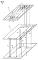
- FIG. 2 is a schematic view showing a more specific configuration example of the display device 10 shown in FIG.
- the display device 10 can have a laminated structure of the layer 40 and the layer 50.
- FIG. 2 shows a configuration in which the layer 50 is provided above the layer 40.
- An interlayer insulating film can be provided between the layer 40 and the layer 50.
- the layer 40 may be provided with a gate driver circuit 22, a data driver circuit 23, a control circuit 31, a storage circuit 32, an arithmetic circuit 33, and a transmission line 34.
- the layer 50 may be provided with a display unit 20.
- the display unit 20 provided on the layer 50 is provided so as to have a region overlapping with the arithmetic circuit 33 provided on the layer 40. Further, the display unit 20 can be provided so as to have an area overlapping with the data driver circuit 23 provided in the layer 40.
- the area of the display unit 20 can be increased by stacking the display unit 20 and the arithmetic circuit 33 and the like so as to have regions that overlap each other. Therefore, since many pixels 21 can be provided on the display unit 20, a high-resolution image can be displayed on the display unit 20. For example, an image having a resolution of 4K2K, 8K4K, or higher can be displayed.
- the display device 10 can be narrowed. Further, by narrowing the frame of the display device 10, the display device 10 can be miniaturized.
- the gate driver circuit 22, the data driver circuit 23, the arithmetic circuit 33, the display unit 20, the wiring 24, and the wiring 25 can be provided on the same chip.
- the control circuit 31 and the storage circuit 32 are provided on the layer 40 as chips different from the chips, and the chips can be electrically connected to each other by the transmission line 34.
- the data driver circuit 23, the arithmetic circuit 33, the display unit 20, the wiring 24, and the wiring 25, the control circuit 31, the storage circuit 32, and the transmission line 34 may all be provided on the same chip. Good.
- the display unit 20 can be provided so as to have an area overlapping the control circuit 31, the storage circuit 32, and the transmission line 34, the area of the display unit 20 can be increased. As a result, many pixels can be provided in the display unit 20, so that a high-resolution image can be displayed on the display unit 20.
- 3A and 3B are diagrams showing an example of arithmetic processing that can be performed by using the storage circuit 32 and the arithmetic circuit 33.
- the image data GD is supplied to the storage circuit 32 and held.
- the arithmetic circuit 33 configured by the neural network NN reads out the image data GD held in the storage circuit 32 and performs arithmetic processing. Data and the like required for arithmetic processing are appropriately read from the storage circuit 32. Further, the calculation result by the calculation circuit 33 can be appropriately written in the storage circuit 32. That is, the arithmetic circuit 33 can perform arithmetic processing on the image data GD while exchanging data and the like with the storage circuit 32.
- the arithmetic circuit 33 supplies the image data to the data driver circuit 23. The image data that has been calculated may be written from the calculation circuit 33 to the storage circuit 32, and then the data driver circuit 23 may read the image data from the storage circuit 32.
- the arithmetic circuit 33 can perform a process of increasing the resolution of the image represented by the image data GD, that is, up-conversion.
- the image data after up-conversion is referred to as image data GD UP Conv .
- a process of restoring the defective portion can be performed on the image data GD including the defective portion.
- the image data after the defective portion is restored is referred to as image data GD Recov .
- the defective portion of the image represented by the image data GD is shown by painting it in black.
- the arithmetic circuit 33 since the arithmetic circuit 33 has a function of up-converting the image data GD, a high-resolution image is displayed on the display unit 20 even if the image resolution represented by the image data GD is low. can do. Therefore, the data capacity of the image data GD can be reduced. Further, as shown in FIG. 3B, since the arithmetic circuit 33 has a function of restoring the defective portion included in the image data GD, the defective portion can be included in the image data GD. Therefore, the data capacity of the image data GD can be reduced.
- the arithmetic circuit 33 may have a function of decompressing compressed image data, for example. As a result, the image data GD can be converted into compressed image data, so that the data capacity of the image data GD can be reduced.
- the up-conversion, the restoration of the defective portion, and the like can be performed with high accuracy. Further, by decompressing the compressed image data GD using the neural network NN, the decompression can be performed with high accuracy. As described above, a high-quality image can be displayed on the display unit 20.
- the display device 10 can display a high-resolution and high-quality image. Further, since the arithmetic circuit 33 has a function of restoring the defective portion included in the image data GD using the neural network NN, the display device 10 can display a high-quality image. Further, since the arithmetic circuit 33 has a function of decompressing the compressed image data GD using the neural network NN, the display device 10 can display a high-quality image.
- FIGS. 4A, 4B, 4C, and 5 are diagrams showing an example of an image data up-conversion method.
- the image data GD corresponding to the image having a resolution of xxy (x, y is an integer of 1 or more) shown in FIG. 4A is the image data corresponding to the image having a resolution of 2xx2y shown in FIG. It shows how to up-convert to GD UP Conv.
- the image data can be configured to have a number of gradation values corresponding to the resolution of the image represented by the image data.
- the image data corresponding to an image having a resolution of xxy can have a configuration having gradation values of x rows and y columns.
- the gradation value means a value representing the gradation of the brightness of the light emitted from the pixels of the display device. For example, the larger the gradation value, the higher the brightness of the light emitted from the pixel.
- the gradation value in the first row and the first column is the gradation value Sa
- the gradation value in the first row and the y column is the gradation value Sb
- x row 1 The gradation value in the column is shown as the gradation value Sc
- the gradation value in the x-row and y-th column is shown as the gradation value Sd.
- each of the gradation values of the image data GD is copied by 2 rows and 2 columns.
- the gradation values of the 1st row 1st column, the 1st row 2nd column, the 2nd row 1st column, and the 2nd row 2nd column are set as the gradation value Sa.
- the gradation values in the 1st row 2y-1st column, the 1st row 2y column, the 2nd row 2y-1st column, and the 2nd row 2y column are defined as the gradation value Sb.
- the gradation values of the 2x-1 row and 1st column, the 2x-1 row and 2nd column, the 2x row and 1st column, and the 2x row and 2nd column are defined as the gradation value Sc. Further, the gradation values of the 2x-1 row 2y-1 column, the 2x-1 row 2y column, the 2x row 2y-1 column, and the 2x row 2y column are defined as the gradation value Sd.
- padding is performed on the image data shown in FIG. 4B. For example, padding is performed for each of the upper and lower rows of the image data and for each of the left and right columns. As padding, zero padding or edge padding can be performed.
- FIG. 4C shows an example in which zero padding is performed for each of the upper and lower rows and one column of the left and right image data.
- the padded image data is input to the neural network NN.
- the product-sum operation is performed between the padded image data and the filter FIL.
- padding is performed for each of the upper and lower rows of the image data and for each of the left and right columns, the filter value has a filter value (weighting coefficient) of 3 rows and 3 columns, and the stride width is set to 1.
- the image data after the product-sum calculation can have gradation values of 2x rows and 2y columns.
- the filter value is acquired in advance by learning.
- the gradation value in the first row and the first column is the gradation value Sa1
- the gradation value in the first row and the second column is the gradation value Sa2, 2.
- the gradation value in the first row and column is the gradation value Sa3, and the gradation value in the second row and second column is the gradation value Sa4.
- the gradation value in the 1st row and 2y-1th column is the gradation value Sb1
- the gradation value in the 1st row and 2y column is the gradation value Sb2
- the gradation value in the 2nd row and 2y-1th column is the gradation value Sb3.
- the gradation value in the second row and the second column is the gradation value Sb4. Further, the gradation value in the 2x-1 row and 1st column is the gradation value Sc1, the gradation value in the 2x-1 row and 2nd column is the gradation value Sc2, and the gradation value in the 2x-1 row and 1st column is the gradation value Sc3. The gradation value in the 2x row and the second column is the gradation value Sc4. Further, the gradation value in the 2x-1 row 2y-1 column is the gradation value Sd1, the gradation value in the 2x-1 row 2y column is the gradation value Sd2, and the gradation value in the 2x row 2y-1 column is the gradation value. The gradation value Sd3 and the gradation value in the 2x row and 2y column are defined as the gradation value Sd4.
- the gradation value Sa1, the gradation value Sa2, the gradation value Sa3, and the gradation value Sa4 can be different values from each other.
- the gradation value Sb1, the gradation value Sb2, the gradation value Sb3, and the gradation value Sb4 can be different values from each other.
- the gradation value Sc1, the gradation value Sc2, the gradation value Sc3, and the gradation value Sc4 can be different values from each other.
- the gradation value Sd1, the gradation value Sd2, the gradation value Sd3, and the gradation value Sd4 can be different values from each other. From the above, the image data after the product-sum calculation can be used as the image data GD UP Conv.
- FIG. 6 is a schematic view showing a configuration example of the display device 10, and is a modification of the display device 10 shown in FIG.
- the display device 10 shown in FIG. 6 is mainly different from the display device 10 shown in FIG. 2 in that two data driver circuits (data driver circuit 23a and data driver circuit 23b) are provided.
- the data driver circuit 23a and the data driver circuit 23b may be collectively referred to as the data driver circuit 23.
- the data driver circuit 23a is electrically connected to, for example, the pixels 21 in the odd-numbered rows. Further, the data driver circuit 23b is electrically connected to, for example, the pixels 21 in the even-numbered columns.
- the data driver circuit 23a has a function of supplying the arithmetically processed image data output by the arithmetic circuit 33 to the pixels 21 in the desired odd-numbered columns via the wiring 25.
- the data driver circuit 23b has a function of supplying the calculated image data output by the arithmetic circuit 33 to the pixels 21 in the desired even-numbered columns via the wiring 25.
- the data driver circuit 23a and the data driver circuit 23b have a function of converting the input image data into analog data, similarly to the data driver circuit 23 shown in FIG.
- the density of transistors and the like constituting the data driver circuits can be reduced. This makes it possible to increase the degree of freedom in the layout of the display device 10.
- FIG. 7 is a schematic view showing a configuration example of the display device 10, and is a modification of the display device 10 shown in FIG.
- the display device 10 shown in FIG. 7 for example, one end of all the wiring 25 is connected to the data driver circuit 23a, and the other end of all the wiring 25 is connected to the data driver circuit 23b.
- the display device 10 shown in FIG. 7 can input image data from both ends of the wiring 25. As a result, it is possible to suppress the attenuation of the image data supplied from the data driver circuit to the pixels 21 due to the wiring resistance of the wiring 25. As a result, the display device 10 can be driven at high speed.
- FIG. 8 is a schematic view showing a configuration example of the display device 10, and is a modification of the display device 10 shown in FIG.
- the display device 10 shown in FIG. 8 is mainly different from the display device 10 shown in FIG. 2 in that the gate driver circuit 22 and the data driver circuit 23 are not clearly separated and have an overlapping region.
- the region where the gate driver circuit 22 and the data driver circuit 23 overlap without being clearly separated is referred to as a region 26.
- the display unit 20 can be provided so as to have an overlapping region with the gate driver circuit 22. As a result, the area of the display unit 20 can be increased. Therefore, since many pixels 21 can be provided on the display unit 20, a high-resolution image can be displayed on the display unit 20.
- FIG. 9 is a diagram showing a configuration example of a region 26 which is a region where the gate driver circuit 22 and the data driver circuit 23 overlap. As shown in FIG. 9, the region 26 is provided with a region having elements constituting the gate driver circuit 22 and a region having elements constituting the data driver circuit 23 with a certain regularity.
- a transistor 71 is shown as an element constituting the gate driver circuit 22, and a transistor 72 is shown as an element constituting the data driver circuit 23.
- FIG. 9 shows a configuration example of the region 26 when the dummy transistor 73 is provided as a dummy element on the four sides of the transistor 71 and the four sides of the transistor 72.
- the transistor 71, the transistor 72, and the dummy transistor 73 are arranged in a matrix, but they may not be arranged in a matrix.
- FIG. 10 is a top view showing a configuration example of the region 70, which is a part of the region 26.
- the region 70 is provided with one transistor 71, one transistor 72, and two dummy transistors 73.
- the transistor 71 has a channel forming region 110, a source region 111, and a drain region 112. Further, the gate electrode 113 is provided so as to have a region overlapping the channel forming region 110.
- FIG. 10 components such as a gate insulator are omitted. Further, in FIG. 10, the channel formation region, the source region, and the drain region are shown without being clearly separated.
- the source region 111 is provided with an opening 114, and the source region 111 is electrically connected to the wiring 115 via the opening 114.
- the drain region 112 is provided with an opening 116, and the drain region 112 is electrically connected to the wiring 117 via the opening 116.
- the gate electrode 113 is provided with an opening 118, and the gate electrode 113 is electrically connected to the wiring 121 via the opening 118.
- the wiring 115 is provided with an opening 119, and the wiring 115 is electrically connected to the wiring 122 through the opening 119.
- the wiring 117 is provided with an opening 120, and the wiring 117 is electrically connected to the wiring 123 via the opening 120. That is, the source region 111 is electrically connected to the wiring 122 via the wiring 115, and the drain region 112 is electrically connected to the wiring 123 via the wiring 117.
- the transistor 72 has a channel forming region 130, a source region 131, and a drain region 132. Further, the gate electrode 133 is provided so as to have a region overlapping the channel forming region 130.
- the source region 131 is provided with an opening 134, and the source region 131 is electrically connected to the wiring 135 via the opening 134.
- the drain region 132 is provided with an opening 136, and the drain region 132 is electrically connected to the wiring 137 via the opening 136.
- the gate electrode 133 is provided with an opening 138, and the gate electrode 133 is electrically connected to the wiring 141 via the opening 138.
- the wiring 135 is provided with an opening 139, and the wiring 135 is electrically connected to the wiring 142 through the opening 139.
- the wiring 137 is provided with an opening 140, and the wiring 137 is electrically connected to the wiring 143 via the opening 140. That is, the source region 131 is electrically connected to the wiring 142 via the wiring 135, and the drain region 132 is electrically connected to the wiring 143 via the wiring 137.
- the channel forming region 110 and the channel forming region 130 can be provided in the same layer. Further, the source region 111 and the drain region 112 and the source region 131 and the drain region 132 can be provided in the same layer. Further, the gate electrode 113 and the gate electrode 133 can be provided in the same layer as each other. Further, the wiring 115 and the wiring 117 and the wiring 135 and the wiring 137 can be provided on the same layer. That is, the transistor 71 and the transistor 72 can be provided in the same layer as each other. As a result, the manufacturing process of the display device 10 can be simplified and the display device 10 can be made inexpensive as compared with the case where the transistor 71 and the transistor 72 are provided in different layers.
- Wiring 121 to 123 that are electrically connected to the transistor 71 that constitutes the gate driver circuit 22 are provided on the same layer as each other. Further, the wirings 141 to 143 that are electrically connected to the transistors 72 that form the data driver circuit 23 are provided on the same layer as each other. Further, the wiring 121 to 123 are provided in a layer different from the wiring 141 to 143. As described above, it is possible to prevent the transistor 71, which is an element constituting the gate driver circuit 22, and the transistor 72, which is an element constituting the data driver circuit 23, from being electrically short-circuited. Therefore, even if the gate driver circuit 22 and the data driver circuit 23 are not clearly separated and have overlapping regions, malfunctions of the gate driver circuit 22 and the data driver circuit 23 can be suppressed. Thereby, the reliability of the display device 10 can be improved.
- FIG. 10 shows a configuration in which the wirings 141 to 143 are provided above the wirings 121 to 123, the wirings 141 to 143 may be provided below the wirings 121 to 123.
- FIG. 10 shows a configuration in which the wiring 121 to 123 extend in the horizontal direction and the wiring 141 to 143 extend in the vertical direction, but one aspect of the present invention is not limited to this.
- the wiring 121 to 123 may be extended in the vertical direction
- the wiring 141 to 143 may be extended in the horizontal direction.
- both the wiring 121 to the wiring 123 and the wiring 141 to 143 may be extended in the horizontal direction or in the vertical direction.
- the dummy transistor 73 includes a semiconductor 151 and a conductor 152.
- the conductor 152 has a region that overlaps with the semiconductor 151.
- the semiconductor 151 can be formed in the same layer as the channel formation region of the transistor 71 and the transistor 72. Further, the conductor 152 can be formed in the same layer as the transistor 71 and the gate electrode of the transistor 72.
- the dummy transistor 73 may be configured not to have either the semiconductor 151 or the conductor 152.
- the semiconductor 151 and the conductor 152 can be configured so as not to be electrically connected to other wiring or the like.
- a constant potential may be supplied to the semiconductor 151 and / or the conductor 152.
- a ground potential may be supplied.
- FIG. 11 is a schematic view showing a configuration example of the display device 10, and is a modification of the display device 10 shown in FIG.
- the display device 10 shown in FIG. 11 is mainly different from the display device 10 shown in FIG. 2 in that the storage circuit 32 is provided on the layer 50.
- the storage circuit 32 may have a configuration in which cells 35 are arranged in a matrix.
- the storage circuit 32 is electrically connected to the control circuit 31 and the arithmetic circuit 33 via the transmission line 34. Specifically, the cell 35 provided in the storage circuit 32 is electrically connected to the control circuit 31 and the arithmetic circuit 33 via the transmission line 34.
- the gate driver circuit 22, the data driver circuit 23, the display unit 20, the wiring 24, and the wiring 25 can be provided on the same chip.
- the control circuit 31, the storage circuit 32, the arithmetic circuit 33, and the transmission line 34 can be provided on the same chip. Therefore, in the display device 10 shown in FIG. 11, the display unit 20 provided on the layer 50 can be provided so as to have an area overlapping with the data driver circuit 23 provided on the layer 40. Further, the storage circuit 32 provided in the layer 50 can be provided so as to have an area overlapping the control circuit 31 and the arithmetic circuit 33 provided in the layer 40.
- the storage circuit 32 can be provided so as to have an area overlapping the control circuit 31 and the arithmetic circuit 33.
- the occupied area of the storage circuit 32 can be increased, so that the data capacity that can be held in the storage circuit 32 can be increased. Therefore, the arithmetic circuit 33 can perform complicated arithmetic processing.
- many arithmetic processes can be performed in parallel. For example, it is possible to perform arithmetic processing in parallel for image data GD of many frames as compared with the case where the data capacity that can be held in the storage circuit 32 is small.
- the display device 10 can be driven at high speed, and for example, the frame frequency of the display device 10 can be increased.
- the chip including the display unit 20, the gate driver circuit 22, and the data driver circuit 23 can be configured not to include the arithmetic circuit 33 and the like. Therefore, the occupied area of the data driver circuit 23 can be increased. For example, the entire display unit 20 can overlap with the data driver circuit 23. By increasing the occupied area of the data driver circuit 23, the density of the transistors and the like constituting the data driver circuit 23 can be reduced. This makes it possible to increase the degree of freedom in the layout of the display device 10.
- the data driver circuit 23 may not be connected to the end of the wiring 25 formed in the layer 50.
- the data driver circuit 23 may be connected to the central portion of the wiring 25 formed in the layer 50.
- the transmission distance of the image data supplied from the data driver circuit 23 to the pixels 21 can be shortened. Therefore, it is possible to suppress the attenuation of the image data supplied to the pixel 21 due to the resistance of the wiring 25. Therefore, the power consumption of the display device 10 can be reduced.
- the display device 10 can be driven at high speed.
- FIG. 12 is a schematic view showing a configuration example of the display device 10, and is a modification of the display device 10 shown in FIG.
- the display device 10 shown in FIG. 12 is mainly different from the display device 10 shown in FIG. 2 in that a layer 60 is provided between the layer 40 and the layer 50.
- a storage circuit 32 is provided on the layer 60. Similar to the display device 10 shown in FIG. 11, the storage circuit 32 may have a configuration in which cells 35 are arranged in a matrix.
- the storage circuit 32 is electrically connected to the control circuit 31 and the arithmetic circuit 33 via the transmission line 34.
- the cell 35 provided in the storage circuit 32 is electrically connected to the control circuit 31 and the arithmetic circuit 33 via the transmission line 34.
- the arithmetic circuit 33 and the cell 35 can be electrically connected via the wiring 36.
- the same number of wires 36 as the cells 35 can be provided.
- the arithmetic circuit 33 provided on the layer 40, the storage circuit 32 provided on the layer 60, and the display unit 20 provided on the layer 50 are provided so as to have an overlapping region. it can. Further, the display unit 20 can be provided so as to have an area overlapping with the data driver circuit 23 provided in the layer 40.
- the occupied area of the storage circuit 32 can be secured. Therefore, the amount of data that can be held in the storage circuit 32 can be increased.
- the arithmetic circuit 33 can perform complicated arithmetic processing.
- many arithmetic processes can be performed in parallel. For example, it is possible to perform arithmetic processing in parallel for image data GD of many frames, as compared with the case where the data capacity that can be held in the storage circuit 32 is small.
- the display device 10 can be driven at high speed, and for example, the frame frequency of the display device 10 can be increased.
- the storage circuit 32 and the arithmetic circuit 33 are electrically connected not only via the transmission line 34 but also via the wiring 36.
- the storage circuit 32 and the arithmetic circuit 33 are electrically connected via the transmission line 34, but the storage circuit 32 and the arithmetic circuit 33 are different from the transmission line 34. May be electrically connected by. As a result, the size of the data flowing through the transmission line 34 can be reduced, so that the display device 10 can be driven at high speed.
- the layer 60 in which the storage circuit 32 is provided is set as one layer, but may be two or more layers.
- FIG. 13 shows a configuration in which the layer 60 is provided with n layers (n is an integer of 2 or more).
- n is an integer of 2 or more.
- the n-layer layer 60 is described as the layer 60_1 to the layer 60_n to distinguish them.
- the display device 10 can be driven at high speed, and for example, the frame frequency of the display device 10 can be increased.
- FIG. 14 is a schematic view showing a configuration example of the display device 10, and is a modification of the display device 10 shown in FIG.
- the display device 10 shown in FIG. 14 is mainly different from the display device 10 shown in FIG. 12 in that the layer 40 is provided between the layer 60 and the layer 50.
- FIG. 14 shows a configuration in which the layer 40 is provided above the layer 60 and the layer 50 is provided above the layer 40.
- the transmission distance of the selection signal supplied from the gate driver circuit 22 to the pixel 21 and the transmission distance of the image data supplied from the data driver circuit 23 to the pixel 21 are displayed as shown in FIG. It can be shorter than the device 10. Therefore, it is possible to suppress the attenuation of the selection signal and the image data supplied to the pixel 21 due to the wiring resistance. Therefore, the power consumption of the display device 10 can be reduced. In addition, the display device 10 can be driven at high speed.
- FIG. 15 is a schematic view showing a configuration example of the display device 10, and is a modification of the display device 10 shown in FIG.
- the display device 10 shown in FIG. 15 is mainly different from the display device 10 shown in FIG. 14 in that the gate driver circuit 22 is provided on the layer 50.
- the transmission distance of the selection signal supplied from the gate driver circuit 22 to the pixels 21 can be further shortened as compared with the display device 10 shown in FIG. Therefore, it is possible to suppress the attenuation of the selection signal supplied to the pixel 21 due to the wiring resistance. Therefore, the power consumption of the display device 10 can be reduced. In addition, the display device 10 can be driven at high speed.
- the gate driver circuit 22 can also be provided in the layer 50 in the display device 10 shown in FIGS. 2, 6, 8, 11, 12, and the like.
- FIG. 16 is a cross-sectional view showing a specific configuration example of the display device 10 shown in FIGS. 2, 6 to 8, 11 and the like.
- the display device 10 has a substrate 701 and a substrate 705, and the substrate 701 and the substrate 705 are bonded to each other by a sealing material 712.
- an insulator substrate, a semiconductor substrate, or a conductor substrate may be used.
- the insulator substrate include a glass substrate, a quartz substrate, a sapphire substrate, a stabilized zirconia substrate (yttria-stabilized zirconia substrate, etc.), a resin substrate, and the like.
- the semiconductor substrate include a semiconductor substrate made of silicon and germanium, and a compound semiconductor substrate made of gallium nitride, silicon carbide, silicon germanium, gallium arsenide, indium phosphide, zinc oxide, and gallium oxide. ..
- the semiconductor substrate having an insulator region inside the above-mentioned semiconductor substrate, for example, an SOI (Silicon On Insulator) substrate and the like.
- the conductor substrate include a graphite substrate, a metal substrate, an alloy substrate, a conductive resin substrate and the like.
- a substrate having a metal nitride a substrate having a metal oxide, and the like.
- a substrate in which a conductor or a semiconductor is provided in an insulator substrate, a substrate in which a conductor or an insulator is provided in a semiconductor substrate, a substrate in which a semiconductor or an insulator is provided in a conductor substrate, and the like.
- a transistor 441 and a transistor 601 are provided on the substrate 701.
- the transistor 441 and the transistor 601 can be a transistor provided in the layer 40.
- the transistor 441 can be, for example, a transistor provided in the control circuit 31, the storage circuit 32, or the arithmetic circuit 33.
- the transistor 441 can be, for example, a transistor provided in the control circuit 31 or the arithmetic circuit 33.
- the transistor 601 can be, for example, a transistor provided in the gate driver circuit 22 or the data driver circuit 23.
- the transistor 441 is composed of a conductor 443 having a function as a gate electrode, an insulator 445 having a function as a gate insulator, and a part of a substrate 701, and is a semiconductor region 447 including a channel forming region and a source region. Alternatively, it has a low resistance region 449a that functions as one of the drain regions and a low resistance region 449b that functions as the other of the source region or the drain region.
- the transistor 441 may be either a p-channel type or an n-channel type.
- the transistor 441 is electrically separated from other transistors by the element separation layer 403.
- FIG. 16 shows a case where the transistor 441 and the transistor 601 are electrically separated by the element separation layer 403.
- the element separation layer 403 can be formed by using a LOCOS (LOCOxidation of Silicon) method, an STI (Shallow Trench Isolation) method, or the like.
- the semiconductor region 447 has a convex shape. Further, the side surface and the upper surface of the semiconductor region 447 are provided so as to be covered with the conductor 443 via the insulator 445. Note that FIG. 16 does not show how the conductor 443 covers the side surface of the semiconductor region 447. Further, a material for adjusting the work function can be used for the conductor 443.
- a transistor having a convex shape in the semiconductor region can be called a fin type transistor because it utilizes the convex portion of the semiconductor substrate.
- it may have an insulator which is in contact with the upper part of the convex portion and has a function as a mask for forming the convex portion.
- FIG. 16 shows a configuration in which a part of the substrate 701 is processed to form a convex portion, the SOI substrate may be processed to form a semiconductor having a convex shape.
- the configuration of the transistor 441 shown in FIG. 16 is an example, and is not limited to the configuration, and may be an appropriate configuration according to the circuit configuration, the circuit driving method, and the like.
- the transistor 441 may be a planar transistor.
- the transistor 601 can have the same configuration as the transistor 441.
- the low resistance region having a function as one of the source region and the drain region of the transistor 601 is defined as the low resistance region 459a. Further, a low resistance region having a function as the other of the source region and the drain region of the transistor 601 is defined as a low resistance region 459b.
- an insulator 405, an insulator 407, an insulator 409, and an insulator 411 are provided.
- the conductor 451 and the conductor 457 are embedded in the insulator 405, the insulator 407, the insulator 409, and the insulator 411.
- the height of the upper surface of the conductor 451 and the conductor 457 can be made the same as the height of the upper surface of the insulator 411.
- An insulator 421 and an insulator 214 are provided on the conductor 451 and the conductor 457, and on the insulator 411.
- a conductor 453 and a conductor 473 are embedded in the insulator 421 and the insulator 214.
- the height of the upper surface of the conductor 453 and the conductor 473 can be made the same as the height of the upper surface of the insulator 214.
- Insulator 216 is provided on the conductor 453, on the conductor 473, and on the insulator 214.
- a conductor 455 and a conductor 475 are embedded in the insulator 216.
- the height of the upper surface of the conductor 455 and the conductor 475 and the height of the upper surface of the insulator 216 can be made about the same.
- Insulator 222, insulator 224, insulator 254, insulator 244, insulator 280, insulator 274, and insulator 281 are provided on the conductor 455, the conductor 475, and the insulator 216.
- the conductor 305 and the conductor 365 are embedded in the insulator 222, the insulator 224, the insulator 254, the insulator 244, the insulator 280, the insulator 274, and the insulator 281.
- the height of the upper surface of the conductor 305 and the conductor 365 can be made the same as the height of the upper surface of the insulator 281.
- the insulator 361 is provided on the conductor 305, the conductor 365, and the insulator 281.
- a conductor 317, a conductor 337, and a conductor 367 are embedded in the insulator 361.
- the height of the upper surface of the conductor 337 and the height of the upper surface of the insulator 361 can be made about the same.
- Insulator 363 is provided on the conductor 337 and on the insulator 361.
- a conductor 347, a conductor 353, a conductor 355, and a conductor 357 are embedded in the insulator 363.
- the height of the upper surface of the conductor 353, the conductor 355, and the conductor 357 can be made the same as the height of the upper surface of the insulator 363.
- Connection electrodes 760 are provided on the conductor 353, on the conductor 355, on the conductor 357, and on the insulator 363. Further, an anisotropic conductor 780 is provided so as to be electrically connected to the connection electrode 760, and an FPC (Flexible Printed Circuit) 716 is provided so as to be electrically connected to the anisotropic conductor 780. Various signals and the like are supplied to the display device 10 from the outside of the display device 10 by the FPC 716.
- FPC Flexible Printed Circuit
- the low resistance region 449b having a function as the other of the source region and the drain region of the transistor 441 includes a conductor 451 and a conductor 453, a conductor 455, a conductor 305, a conductor 317, and a conductor. It is electrically connected to the FPC 716 via 337, a conductor 347, a conductor 353, a conductor 355, a conductor 357, a connection electrode 760, and an anisotropic conductor 780.
- FIG. 16 shows three conductors having a function of electrically connecting the connection electrode 760 and the conductor 347, that is, the conductor 353, the conductor 355, and the conductor 357, which is one of the present inventions.
- the aspect is not limited to this.
- the number of conductors having a function of electrically connecting the connection electrode 760 and the conductor 347 may be one, two, or four or more.
- the contact resistance can be reduced by providing a plurality of conductors having a function of electrically connecting the connection electrode 760 and the conductor 347.
- the low resistance region 459a having a function as one of the source region and the drain region of the transistor 601 is formed via the conductor 457, the conductor 473, the conductor 475, and the conductor 365. It is electrically connected to the conductor 367.
- a transistor 750 is provided on the insulator 214.
- the transistor 750 can be a transistor provided on the layer 50. Specifically, it can be a transistor provided in the display unit 20.
- the transistor included in the storage circuit 32 can be provided on the same layer as the transistor 750.
- the same layer as A means, for example, a layer having the same material formed in the same step as A.
- a transistor (also referred to as an OS transistor) using a metal oxide in the channel forming region can be preferably used.
- the metal oxide is a metal oxide in a broad sense. Metal oxides are classified into oxide insulators, oxide conductors (including transparent oxide conductors), oxide semiconductors (also referred to as Oxide Semiconductor or simply OS) and the like. For example, when a metal oxide is used in the channel forming region of a transistor, the metal oxide may be referred to as an oxide semiconductor. That is, when it is described as an OS transistor, it can be rephrased as a transistor having an oxide or an oxide semiconductor.
- the OS transistor Since the OS transistor has a large energy gap in the semiconductor layer, it can exhibit an extremely small off-current characteristic in which the off-current value per 1 ⁇ m of the channel width is several yA / ⁇ m (y is 10-24). Therefore, since the holding time of the image data or the like can be lengthened, the frequency of the refresh operation can be reduced. Therefore, the power consumption of the display device 10 can be reduced.
- a metal oxide having an energy gap of 2 eV or more, preferably 2.2 eV or more, more preferably 2.5 eV or more can be used.
- a typical example is an oxide semiconductor containing indium, and for example, CAAC-OS (C-Axis Defined Crystalline Semiconductor) or CAC-OS (Cloud-Aligned Compound Semiconductor), which will be described later, can be used.
- CAAC-OS has a stable crystal structure and is suitable for transistors and the like in which reliability is important. Further, CAC-OS is suitable for a transistor or the like that performs high-speed driving because it exhibits high mobility characteristics.
- the semiconductor layer of the OS transistor is an In-M-Zn-based oxidation containing, for example, indium, zinc and element M (one or more of aluminum, titanium, gallium, germanium, yttrium, zirconium, lanthanum, cerium, tin, neodymium or hafnium). It can be a film represented by an object.
- indium, zinc and element M one or more of aluminum, titanium, gallium, germanium, yttrium, zirconium, lanthanum, cerium, tin, neodymium or hafnium.
- the conductor 301a and the conductor 301b are embedded in the insulator 254, the insulator 244, the insulator 280, the insulator 274, and the insulator 281.
- the conductor 301a is electrically connected to one of the source or drain of the transistor 750
- the conductor 301b is electrically connected to the other of the source or drain of the transistor 750.
- the height of the upper surfaces of the conductors 301a and 301b and the height of the upper surfaces of the insulator 281 can be made about the same.
- a conductor 311 and a conductor 313, a conductor 331, a capacitor 790, a conductor 333, and a conductor 335 are embedded in the insulator 361.
- the capacitor 790 can be, for example, a capacitor provided in the display unit 20.
- the capacitor 790 can be, for example, a capacitor provided in the storage circuit 32.
- the conductors 311 and 313 are electrically connected to the transistor 750 and have a function as wiring.
- the conductor 333 and the conductor 335 are electrically connected to the capacitor 790.
- the height of the upper surface of the conductor 331, the conductor 333, and the conductor 335 can be made the same as the height of the upper surface of the insulator 361.
- the conductor 367 can be formed in the same layer as the conductor 311 and the conductor 313, and the conductor 317.
- the conductor 367 can be electrically connected to an element such as a transistor provided in the layer 50, that is, a transistor or the like provided in the same layer as the transistor 750.
- the conductor 367 can be electrically connected to a transistor provided on the display unit 20.
- a conductor 341, a conductor 343, and a conductor 351 are embedded in the insulator 363.
- the conductor 343 is provided on the insulator 361, the conductor 333, and the conductor 335.
- the height of the upper surface of the conductor 351 and the height of the upper surface of the insulator 363 can be made about the same.
- Insulator 405, insulator 407, insulator 409, insulator 411, insulator 421, insulator 214, insulator 280, insulator 274, insulator 281, insulator 361, and insulator 363 are used as interlayer films. It may have a function and may have a function as a flattening film that covers each lower uneven shape. For example, the upper surface of the insulator 363 may be flattened by a flattening treatment using a chemical mechanical polishing (CMP) method or the like in order to improve the flatness.
- CMP chemical mechanical polishing
- the upper surfaces of the insulator 405, the insulator 407, the insulator 409, the insulator 411, the insulator 421, the insulator 214, the insulator 280, the insulator 274, the insulator 281 and the insulator 361 are also subjected to the CMP method or the like. It may be flattened by the flattening treatment used.
- the capacitor 790 has a lower electrode 321 and an upper electrode 325. Further, an insulator 323 is provided between the lower electrode 321 and the upper electrode 325. That is, the capacitor 790 has a laminated structure in which an insulator 323 having a function as a dielectric is sandwiched between a pair of electrodes.
- FIG. 16 shows an example in which the capacitor 790 is provided on the insulator 281, the capacitor 790 may be provided on an insulator different from the insulator 281.
- FIG. 16 shows an example in which the conductor 301a, the conductor 301b, the conductor 305, and the conductor 365 are formed in the same layer. Further, an example is shown in which the conductor 311 and the conductor 313, the conductor 317, the conductor 367, and the lower electrode 321 are formed in the same layer. Further, an example is shown in which the conductor 331, the conductor 333, the conductor 335, and the conductor 337 are formed in the same layer. Further, an example is shown in which the conductor 341, the conductor 343, and the conductor 347 are formed in the same layer. Further, an example is shown in which the conductor 351 and the conductor 353, the conductor 355, and the conductor 357 are formed in the same layer. By forming a plurality of conductors in the same layer, the manufacturing process of the display device 10 can be simplified, so that the display device 10 can be made inexpensive. In addition, these may be formed in different layers, and may have different kinds of materials.
- the display device 10 shown in FIG. 16 has a light emitting element 500.
- the light emitting element can also be referred to as a light emitting device.
- the light emitting element 500 has a conductor 772, an EL layer 786, and a conductor 788.
- the EL layer 786 has an organic compound or an inorganic compound such as a quantum dot.
- Examples of the material that can be used for the organic compound include a fluorescent material and a phosphorescent material.
- Examples of materials that can be used for quantum dots include colloidal quantum dot materials, alloy-type quantum dot materials, core-shell type quantum dot materials, and core-type quantum dot materials.
- the conductor 772 is electrically connected to the other of the source or drain of the transistor 750 via the conductor 351 and the conductor 341, the conductor 331, the conductor 313, and the conductor 301b.
- the conductor 772 is formed on the insulator 363 and has a function as a pixel electrode.
- a material that is transparent to visible light or a material that is reflective can be used.
- the translucent material for example, an oxide material containing indium, zinc, tin, etc. may be used.
- the reflective material for example, a material containing aluminum, silver, or the like may be used.
- the display device 10 can be provided with an optical member (optical substrate) such as a polarizing member, a retardation member, and an antireflection member.
- an optical member optical substrate
- polarizing member such as a polarizing member, a retardation member, and an antireflection member.
- a light-shielding layer 738 and an insulator 734 are provided on the substrate 705 side.
- the insulator 734 has a region in contact with the light shielding layer 738.
- the light-shielding layer 738 has a function of blocking light emitted from an adjacent region.
- the light-shielding layer 738 has a function of blocking external light from reaching the transistor 750 or the like.
- an insulator 730 is provided on the insulator 363.
- the insulator 730 can be configured to cover a part of the conductor 772.
- the light emitting element 500 has a translucent conductor 788, and can be a top emission type light emitting element.
- the light emitting element 500 may have a bottom emission structure that emits light to the conductor 772 side, or a dual emission structure that emits light to both the conductor 772 side and the conductor 788 side.
- the light-shielding layer 738 is provided so as to have a region overlapping with the insulator 730. Further, the light-shielding layer 738 is covered with an insulator 734. Further, the space between the light emitting element 500 and the insulator 734 is filled with a sealing layer 732.
- the structure 778 is provided between the insulator 730 and the EL layer 786. Further, the structure 778 is provided between the insulator 730 and the insulator 734.
- the display device 10 shown in FIG. 16 is provided with a colored layer 736.
- the colored layer 736 is provided so as to have a region overlapping with the light emitting element 500.
- the coloring layer 736 By providing the coloring layer 736, the color purity of the light extracted from the light emitting element 500 can be increased. As a result, a high-quality image can be displayed on the display device 10.
- the EL layer 786 does not have to be formed by painting separately, and the pixels 21 can be miniaturized. .. Therefore, the density of the pixels 21 provided in the display unit 20 can be increased, and a high-definition image can be displayed on the display device 10.
- FIG. 17 is a cross-sectional view showing a specific configuration example of the display device 10, and is a modification of the display device 10 shown in FIG.
- the display device 10 shown in FIG. 17 is different from the display device 10 shown in FIG. 16 in that a transistor 800 and a capacitor 890 are provided between the layer having the transistor 750 and the layer having the transistor 441 and the transistor 601. Mainly different.
- the configuration shown in FIG. 17 can be applied to the display device 10 shown in FIG. 12 and the like.
- the transistor 800 and the capacitor 890 can be provided on the layer 60. That is, the transistor 800 and the capacitor 890 can be provided in the storage circuit 32.
- the insulator 821 and the insulator 814 are provided on the conductor 451 and the conductor 457, and on the insulator 411.
- the conductor 853 and the conductor 857 are embedded in the insulator 821 and in the insulator 814.
- the height of the upper surface of the conductor 853 and the conductor 857 can be made the same as the height of the upper surface of the insulator 814.
- the insulator 816 is provided on the conductor 853, the conductor 857, and the insulator 814.
- a conductor 855 and a conductor 859 are embedded in the insulator 816.
- the height of the upper surface of the conductor 855 and the conductor 859 can be made the same as the height of the upper surface of the insulator 816.
- Insulator 822, insulator 824, insulator 854, insulator 844, insulator 880, insulator 874, and insulator 881 are provided on the conductor 855, the conductor 859, and the insulator 816.
- the conductor 805 and the conductor 861 are embedded in the insulator 822, the insulator 824, the insulator 854, the insulator 844, the insulator 880, the insulator 874, and the insulator 881.
- the height of the upper surface of the conductor 805 and the conductor 861 can be made the same as the height of the upper surface of the insulator 881.
- Insulator 883 is provided on the conductor 805, on the conductor 861, and on the insulator 881.
- a conductor 817, a conductor 831, a conductor 863, and a conductor 865 are embedded in the insulator 883.
- the height of the upper surface of the conductor 831 and the conductor 865 can be made the same as the height of the upper surface of the insulator 883.
- the insulator 421 and the insulator 214 are provided on the conductor 831, the conductor 865, and the insulator 883.
- a conductor 833 and a conductor 867 are embedded in the insulator 421.
- the conductor 453 and the conductor 473 are embedded in the insulator 421 and the insulator 214.
- the height of the upper surface of the conductor 453 and the conductor 473 can be made the same as the height of the upper surface of the insulator 214.
- the low resistance region 449b having a function as the other of the source region and the drain region of the transistor 441 includes a conductor 451 and a conductor 853, a conductor 855, a conductor 805, a conductor 817, and a conductor. 831, conductor 833, conductor 453, conductor 455, conductor 305, conductor 317, conductor 337, conductor 347, conductor 353, conductor 355, conductor 357, connection electrode 760, and anisotropic It is electrically connected to the FPC 716 via a conductor 780.
- the low resistance region 459a having a function as one of the source region and the drain region of the transistor 601 includes a conductor 457, a conductor 857, a conductor 859, a conductor 861, and a conductor 863. It is electrically connected to the conductor 367 via the conductor 865, the conductor 867, the conductor 473, the conductor 475, and the conductor 365.
- a transistor 800 is provided on the insulator 814. As described above, the transistor 800 can be a transistor provided on the layer 60. For example, in the display device 10 shown in FIG. 12, the transistor 800 can be a transistor provided in the storage circuit 32. The transistor 800 is preferably an OS transistor.
- Conductors 801a and 801b are embedded in the insulator 854, the insulator 844, the insulator 880, the insulator 874, and the insulator 881.
- the conductor 801a is electrically connected to one of the source or drain of the transistor 800
- the conductor 801b is electrically connected to the other of the source or drain of the transistor 800.
- the heights of the upper surfaces of the conductors 801a and 801b and the heights of the upper surfaces of the insulator 881 can be made about the same.
- a conductor 811, a capacitor 890, a conductor 893, and a conductor 895 are embedded in the insulator 883.
- the capacitor 890 can have the same configuration as the capacitor 790.
- the capacitor 890 can be, for example, a capacitor provided in the storage circuit 32.
- the conductor 811 is electrically connected to the transistor 800 and has a function as wiring.
- the conductor 801b is electrically connected to one electrode of the capacitor 890 in addition to the transistor 800.
- the conductor 893 and the conductor 895 are electrically connected to the other electrode of the capacitor 890.
- the height of the upper surface of the conductor 893 and the conductor 895 can be made the same as the height of the upper surface of the insulator 883.
- a conductor 897 is embedded in the insulator 421.
- the conductor 897 is provided on the insulator 883, on the conductor 893, and on the conductor 895.
- the insulator 821, the insulator 814, the insulator 880, the insulator 874, the insulator 881, and the insulator 883 have a function as an interlayer film, and a function as a flattening film that covers the uneven shape below each of them. May have.
- FIG. 17 shows an example in which the conductor 801a, the conductor 801b, the conductor 805, and the conductor 861 are formed in the same layer. Further, an example is shown in which the conductor 811, the conductor 817, and the conductor 863 are formed in the same layer. Further, an example is shown in which the conductor 893, the conductor 895, the conductor 831, and the conductor 865 are formed in the same layer. Further, an example is shown in which the conductor 897, the conductor 833, and the conductor 867 are formed in the same layer. As described above, by forming the plurality of conductors in the same layer, the manufacturing process of the display device 10 can be simplified, so that the manufacturing cost of the display device 10 can be reduced. In addition, these may be formed in different layers, and may have different kinds of materials.
- FIG. 18 is a cross-sectional view showing a specific configuration example of the display device 10 shown in FIG. 14 or FIG.
- a substrate 901 is provided on the layer 60, and a transistor 911 is provided on the substrate 901.
- a substrate 903 is provided on the layer 40, and a transistor 913, a transistor 915, and a transistor 917 are provided on the substrate 903.
- a substrate 905 is provided on the layer 50, and a transistor 919 is provided on the substrate 905. Then, each of the substrate 901, the substrate 903, and the substrate 905 is bonded by bonding.
- the substrate 901, the substrate 903, and the substrate 905 can have the same configuration as the substrate 701.
- the transistor 911, the transistor 913, the transistor 915, the transistor 917, and the transistor 919 can have the same configuration as the transistor 441 and the transistor 601.
- the transistor 911 can be, for example, a transistor provided in the storage circuit 32.
- the transistor 913 and the transistor 917 can be a transistor provided in the control circuit 31 or the arithmetic circuit 33.
- the transistor 915 can be a transistor provided in the data driver circuit 23.
- the transistor 919 can be a transistor provided on the display unit 20.
- the transistor 915 can be a transistor provided in the gate driver circuit 22.
- An insulator 921 and an insulator 923 are provided between the transistor 911, the transistor 913, the transistor 915, and the transistor 917.
- An insulator 925 and an insulator 927 are provided between the transistor 913, the transistor 915, the transistor 917, and the transistor 919.
- a conductor 931 is embedded in the insulator 921. Further, a conductor 937, a conductor 939, and a conductor 941 are embedded in the insulator 925.
- the conductor 931 is flattened so that the height matches that of the insulator 921. Further, the conductor 937, the conductor 939, and the conductor 941 are flattened so as to have the same height as the insulator 925.
- the conductor 933 is provided so as to have a region embedded in the insulator 923 and the substrate 903.
- the conductor 933 has a region covered with the insulator 935 in order to insulate the substrate 903.
- the conductor 931 and the conductor 937 are electrically connected to each other via the conductor 933.
- One of the source region or the drain region of the transistor 911 and one of the source region or the drain region of the transistor 913 are electrically connected via the conductor 931, the conductor 933, and the conductor 937.
- the conductor 943 and the conductor 947 are provided so as to have a region embedded in the insulator 927 and the substrate 905.
- the conductor 943 has a region covered with an insulator 945 in order to insulate the substrate 905.
- the conductor 947 has a region covered with an insulator 949 in order to insulate the substrate 905.
- the conductor 943 is electrically connected to the conductor 939, and the conductor 947 is electrically connected to the conductor 941. Further, the conductor 943 is electrically connected to the conductor 951 provided on the conductor 943 and the insulator 945, and the conductor 947 is electrically connected to the FPC 716.
- the conductor 951 can be electrically connected to an element such as a transistor provided in the layer 50, that is, a transistor or the like provided in the same layer as the transistor 919.
- the conductor 951 can be electrically connected to a transistor provided in the pixel 21.
- One of the source region or the drain region of the transistor 915 and the conductor 951 are electrically connected via the conductor 939 and the conductor 943.
- One of the source region or the drain region of the transistor 917 and the FPC 716 are electrically connected to each other via the conductor 941 and the conductor 947.
- One of the source region and the drain region of the transistor 919 is electrically connected to the light emitting element 500.
- the conductor 933 is provided so as to penetrate the substrate 903. Further, the conductor 943 and the conductor 947 are provided so as to penetrate the substrate 905. Therefore, it can be said that the conductor 933, the conductor 943, and the conductor 947 are through electrodes.
- the substrate 903 is a substrate having silicon (also referred to as a silicon substrate)
- the conductor 933 is a TSV (Through Silicon Via).
- the substrate 905 is a silicon substrate
- the conductor 943 and the conductor 947 are TSVs.
- the layer 60 and the layer 40 are joined so as to have mechanical strength. Further, by bonding the insulator 925 and the insulator 927, the layer 40 and the layer 50 are joined so as to have mechanical strength.
- the transistor 913, the transistor 915, and the transistor 917 can be a transistor (also referred to as a Si transistor) using silicon in the channel forming region. Therefore, the transistor constituting the data driver circuit 23, the control circuit 31, the arithmetic circuit 33, etc. provided on the layer 40 can be a Si transistor. Further, in the display device shown in FIG. 14, the transistor constituting the gate driver circuit 22 can be a Si transistor. If the substrate 905 is a silicon substrate, the transistor constituting the gate driver circuit 22 can also be a Si transistor in the display device 10 shown in FIG.
- the Si transistor Since the Si transistor has a feature of having a large on-current, a circuit or the like composed of the Si transistor can be driven at high speed.
- a through electrode is provided on the substrate 903 provided on the layer 40, and the transistor or the like provided on the layer 60 and the transistor or the like provided on the layer 40 are electrically connected via the through electrode. Therefore, while the layer 40 is provided between the layer 60 and the layer 50, the circuit or the like provided on the layer 40 can be driven at high speed. Therefore, the layer 60 has both the transmission distance of the selection signal supplied from the gate driver circuit 22 to the pixel 21 and the transmission distance of the image data signal supplied from the data driver circuit 23 to the pixel 21.
- the circuit and the like provided in the layer 40 can be driven at high speed while being shorter than the case provided between 50. Therefore, the display device 10 can be driven at high speed while reducing the power consumption of the display device 10.
- FIG. 19 shows a configuration in which the insulator 421 and the insulator 214 shown in FIGS. 16 and 17 are provided on the insulator 925.
- the configuration of the layer above the insulator 214 can be the same as in FIGS. 16 and 17.
- an OS transistor can be provided on the insulator 214.
- FIG. 16 and 17 show a configuration in which the transistor 441 and the transistor 601 are provided so that a channel forming region is formed inside the substrate 701, and the OS transistor is provided by laminating the transistor 441 and the transistor 601.
- FIG. 20 is a modification of the display device 10 shown in FIG. 16, and the point that the OS transistor 602 and the transistor 603 are provided instead of the transistor 441 and the transistor 601 is mainly the display device 10 shown in FIG. different.
- the transistor 750 an OS transistor can be used. That is, the display device 10 shown in FIG. 20 is provided with OS transistors stacked.
- An insulator 613 and an insulator 614 are provided on the substrate 701, and a transistor 602 and a transistor 603 are provided on the insulator 614.
- the transistor 602 and the transistor 603 can be, for example, a transistor included in the gate driver circuit 22 provided in the layer 40 or the data driver circuit 23. ..
- the transistor 602 and the transistor 603 can be a transistor having the same configuration as the transistor 750.
- the transistor 602 and the transistor 603 may be OS transistors having a configuration different from that of the transistor 750.
- an insulator 616, an insulator 622, an insulator 624, an insulator 654, an insulator 644, an insulator 680, an insulator 674, and an insulator 681 are provided on the insulator 614. ..
- the conductor 461 and the conductor 465 are embedded in the insulator 654, the insulator 644, the insulator 680, the insulator 674, and the insulator 681.
- the height of the upper surface of the conductor 461 and the conductor 465 can be made the same as the height of the upper surface of the insulator 681.
- An insulator 421 and an insulator 214 are provided on the conductor 461, the conductor 465, and the insulator 681.
- a conductor 463 and a conductor 467 are embedded in the insulator 421.
- the conductor 453 and the conductor 473 are embedded in the insulator 421 and the insulator 214.
- the height of the upper surface of the conductor 453 and the conductor 473 can be made the same as the height of the upper surface of the insulator 214.
- one of the source and drain of the transistor 602 is a conductor 461, a conductor 463, a conductor 453, a conductor 455, a conductor 305, a conductor 317, a conductor 337, a conductor 347, and a conductor. It is electrically connected to the FPC 716 via a body 353, a conductor 355, a conductor 357, a connection electrode 760, and an anisotropic conductor 780. Further, one of the source and drain of the transistor 603 is electrically connected to the conductor 367 via the conductor 465, the conductor 467, the conductor 473, the conductor 475, and the conductor 365.
- the insulator 613, the insulator 614, the insulator 680, the insulator 674, and the insulator 681 have a function as an interlayer film, and have a function as a flattening film that covers the uneven shape below each of them. May be good.
- all the transistors included in the display device 10 can be the same type of transistors.
- all the transistors included in the display device 10 can be OS transistors.
- the transistor provided in the layer 40 and the transistor provided in the layer 50 can be manufactured by using the same device. Therefore, the manufacturing cost of the display device 10 can be reduced, and the display device 10 can be made inexpensive.
- FIG. 16 to 20 show a configuration in which a light emitting element is provided in the display device 10 as a display element (also referred to as a display device), but one aspect of the present invention is not limited to this.
- FIG. 21 is a modification of the display device 10 shown in FIG. 16, which is mainly different from the display device 10 shown in FIG. 16 in that it has a liquid crystal element 510 instead of the light emitting element 500.
- the liquid crystal element 510 has a conductor 772, a conductor 774, and a liquid crystal layer 776 between them.
- the liquid crystal element can also be referred to as a liquid crystal device.
- the conductor 774 is provided on the substrate 705 side and has a function as a common electrode.
- the conductor 772 is electrically connected to the other of the source or drain of the transistor 750 via the conductor 351 and the conductor 341, the conductor 331, the conductor 313, and the conductor 301b.
- the conductor 772 is formed on the insulator 363 and has a function as a pixel electrode.
- a material that is transparent to visible light or a material that is reflective can be used.
- the translucent material for example, an oxide material containing indium, zinc, tin, etc. may be used.
- the reflective material for example, a material containing aluminum, silver, or the like may be used.
- the display device 10 When a reflective material is used for the conductor 772, the display device 10 becomes a reflective liquid crystal display device. On the other hand, if a translucent material is used for the conductor 772 and a translucent material is also used for the substrate 701 or the like, the display device 10 becomes a transmissive liquid crystal display device. When the display device 10 is a reflective liquid crystal display device, a polarizing plate is provided on the viewing side. On the other hand, when the display device 10 is a transmissive liquid crystal display device, a pair of polarizing plates are provided so as to sandwich the liquid crystal element.
- an alignment film in contact with the liquid crystal layer 776 may be provided.
- an optical member optical substrate
- a polarizing member such as a polarizing member, a retardation member, and an antireflection member
- a light source such as a backlight and a side light
- a structure 778 is provided between the insulator 363 and the conductor 774.
- the structure 778 is a columnar spacer and has a function of controlling the distance (cell gap) between the substrate 701 and the substrate 705.
- a spherical spacer may be used as the structure 778.
- the liquid crystal layer 776 includes a thermotropic liquid crystal, a low molecular weight liquid crystal, a polymer liquid crystal, a polymer dispersed liquid crystal (PDLC: Polymer Dispersed Liquid Crystal), a polymer network type liquid crystal (PNLC: Polymer Network Liquid Crystal), and a strong dielectric liquid crystal. , Anti-strong dielectric liquid crystal and the like can be used. Further, when the transverse electric field method is adopted, a liquid crystal showing a blue phase without using an alignment film may be used.
- the modes of the liquid crystal element include TN (Twisted Nematic) mode, VA (Vertical Birefringence) mode, IPS (In-Plane-Switching) mode, FFS (Fringe Field Switching) mode, and ASM (Axial symmetry). Mode, OCB (Optically Compensated Birefringence) mode, ECB (Electrically Controlled Birefringence) mode, guest host mode and the like can be used.
- a scattering type liquid crystal in which a polymer-dispersed liquid crystal, a polymer network-type liquid crystal, or the like is used for the liquid crystal layer 776 can also be used.
- a black-and-white display may be performed without providing the colored layer 736, or a color display may be performed using the colored layer 736.
- a time division display method (also referred to as a field sequential driving method) in which color display is performed based on a time-addition color mixing method may be applied.
- the structure may be such that the colored layer 736 is not provided.
- the time division display method it is not necessary to provide pixels exhibiting the respective colors of R (red), G (green), and B (blue), so that the aperture ratio of the pixels can be improved. There are advantages such as being able to increase the definition.
- Transistor configuration example> 22A, 22B, and 22C are a top view and a cross-sectional view of the transistor 200A and the periphery of the transistor 200A that can be used in the display device according to one aspect of the present invention.
- the transistor 200A can be applied to the transistor 750 shown in FIGS. 16, 17, and 19 to 21.
- the transistor 200A can be applied to the transistor 800 shown in FIG. 17 and the transistors 602 and 603 shown in FIG. 20.
- FIG. 22A is a top view of the transistor 200A.
- 22B and 22C are cross-sectional views of the transistor 200A.
- FIG. 22B is a cross-sectional view of the portion shown by the alternate long and short dash line of A1-A2 in FIG. 22A, and is also a cross-sectional view of the transistor 200A in the channel length direction.
- FIG. 22C is a cross-sectional view of the portion shown by the alternate long and short dash line of A3-A4 in FIG. 22A, and is also a cross-sectional view of the transistor 200A in the channel width direction.
- some elements are omitted for the sake of clarity.
- the conductor 200A is composed of a metal oxide 230a arranged on a substrate (not shown), a metal oxide 230b arranged on the metal oxide 230a, and a metal oxide 230b.
- Insulator 280 arranged above the conductors 242a and 242b separated from each other and on the conductors 242a and 242b and having an opening formed between the conductors 242a and the conductors 242b.
- the conductor 260 arranged in the opening, the metal oxide 230b, the conductor 242a, the conductor 242b, the insulator 280, the insulator 250 arranged between the conductor 260, and the metal.
- the conductor 242a and the conductor 242b may be collectively referred to as a conductor 242.
- the side surfaces of the conductor 242a and the conductor 242b on the conductor 260 side have a substantially vertical shape.
- the transistor 200A shown in FIG. 22 is not limited to this, and the angle formed by the side surface and the bottom surface of the conductor 242a and the conductor 242b is 10 ° or more and 80 ° or less, preferably 30 ° or more and 60 ° or less. May be. Further, the opposing side surfaces of the conductor 242a and the conductor 242b may have a plurality of surfaces.
- the insulator 254 is arranged between the insulator 224, the metal oxide 230a, the metal oxide 230b, the conductor 242a, the conductor 242b, the metal oxide 230c, and the insulator 280. Is preferable.
- the insulator 254 includes a side surface of the metal oxide 230c, an upper surface and a side surface of the conductor 242a, an upper surface and a side surface of the conductor 242b, a metal oxide 230a and a metal oxide 230b. It is preferable to be in contact with the side surface of the insulator and the upper surface of the insulator 224.
- the transistor 200A has a configuration in which three layers of a metal oxide 230a, a metal oxide 230b, and a metal oxide 230c are laminated in a region where a channel is formed (hereinafter, also referred to as a channel formation region) and in the vicinity thereof.
- a two-layer structure of the metal oxide 230b and the metal oxide 230c, or a laminated structure of four or more layers may be provided.
- the conductor 260 is shown as a two-layer laminated structure, but one aspect of the present invention is not limited to this.
- the conductor 260 may have a single-layer structure or a laminated structure of three or more layers.
- each of the metal oxide 230a, the metal oxide 230b, and the metal oxide 230c may have a laminated structure of two or more layers.
- the metal oxide 230c has a laminated structure composed of a first metal oxide and a second metal oxide on the first metal oxide
- the first metal oxide is a metal oxide 230b. It has a similar composition
- the second metal oxide preferably has the same composition as the metal oxide 230a.
- the conductor 260 functions as a gate electrode of the transistor, and the conductor 242a and the conductor 242b each function as a source electrode or a drain electrode.
- the conductor 260 is formed so as to be embedded in the opening of the insulator 280 and the region sandwiched between the conductor 242a and the conductor 242b.
- the arrangement of the conductor 260, the conductor 242a, and the conductor 242b is selected in a self-aligned manner with respect to the opening of the insulator 280. That is, in the transistor 200A, the gate electrode can be arranged in a self-aligned manner between the source electrode and the drain electrode.
- the conductor 260 can be formed without providing the alignment margin, the occupied area of the transistor 200A can be reduced.
- the pixels provided in the display device can be miniaturized, so that the pixel density can be increased and a high-definition image can be displayed on the display device.
- the density of the pixels 21 provided on the display unit 20 of the display device 10 can be 1000 ppi or more, 3000 ppi or more, 5000 ppi or more, or 7000 ppi or more. Therefore, a high-quality image with less graininess can be displayed on the display device 10, and an image with a high sense of presence can be displayed.
- the display device 10 can be suitably used for a wearable type electronic device, a stationary type electronic device, or the like, which can be used as an electronic device for AR or VR.
- the display device 10 can be suitably used for HMDs and eyeglass-type electronic devices.
- the conductor 260 preferably has a conductor 260a provided inside the insulator 250 and a conductor 260b provided so as to be embedded inside the conductor 260a.
- the transistor 200A includes an insulator 214 arranged on a substrate (not shown), an insulator 216 arranged on the insulator 214, and a conductor 205 arranged so as to be embedded in the insulator 216. It is preferable to have an insulator 222 arranged on the insulator 216 and the conductor 205, and an insulator 224 arranged on the insulator 222. It is preferable that the metal oxide 230a is arranged on the insulator 224.
- an insulator 274 having a function as an interlayer film and an insulator 281 are arranged on the transistor 200A.
- the insulator 274 is arranged in contact with the upper surface of the conductor 260, the insulator 250, the insulator 254, the metal oxide 230c, and the insulator 280.
- the insulator 222, the insulator 254, and the insulator 274 preferably have a function of suppressing the diffusion of at least one hydrogen (for example, a hydrogen atom, a hydrogen molecule, etc.).
- the insulator 222, the insulator 254, and the insulator 274 preferably have lower hydrogen permeability than the insulator 224, the insulator 250, and the insulator 280.
- the insulator 222 and the insulator 254 preferably have a function of suppressing the diffusion of at least one oxygen (for example, oxygen atom, oxygen molecule, etc.).
- the insulator 222 and the insulator 254 preferably have lower oxygen permeability than the insulator 224, the insulator 250, and the insulator 280.
- the insulator 224, the metal oxide 230, and the insulator 250 are separated from the insulator 280 and the insulator 281 by the insulator 254 and the insulator 274. Therefore, in the insulator 224, the metal oxide 230, and the insulator 250, impurities such as hydrogen contained in the insulator 280 and the insulator 281 or excess oxygen are added to the insulator 224, the metal oxide 230a, and the metal oxide. It is possible to suppress mixing with 230b and the insulator 250.
- a conductor 240 (conductor 240a and conductor 240b) that is electrically connected to the transistor 200A and has a function as a plug is provided.
- An insulator 241 (insulator 241a and insulator 241b) is provided in contact with the side surface of the conductor 240 having a function as a plug. That is, the insulator 254, the insulator 280, the insulator 274, and the insulator 241 are provided in contact with the inner wall of the opening of the insulator 281. Further, the first conductor of the conductor 240 may be provided in contact with the side surface of the insulator 241, and the second conductor of the conductor 240 may be further provided inside.
- the height of the upper surface of the conductor 240 and the height of the upper surface of the insulator 281 can be made about the same.
- the transistor 200A shows a configuration in which the first conductor of the conductor 240 and the second conductor of the conductor 240 are laminated, one aspect of the present invention is not limited to this.
- the conductor 240 may be provided as a single layer or a laminated structure having three or more layers. When the structure has a laminated structure, an ordinal number may be given in the order of formation to distinguish them.
- the transistor 200A is a metal oxide 230 (metal oxide 230a, metal oxide 230b, and metal oxide 230c) containing a channel forming region, and a metal oxide having a function as an oxide semiconductor (hereinafter, also referred to as an oxide semiconductor). It is preferable to use.).
- the metal oxide preferably contains at least indium (In) or zinc (Zn). In particular, it preferably contains indium (In) and zinc (Zn). Further, in addition to these, it is preferable that the element M is contained.
- Elements M include aluminum (Al), gallium (Ga), yttrium (Y), tin (Sn), boron (B), titanium (Ti), iron (Fe), nickel (Ni), germanium (Ge), and zirconium.
- the element M is preferably one or more of aluminum (Al), gallium (Ga), yttrium (Y), or tin (Sn). Further, it is more preferable that the element M has either one or both of Ga and Sn.
- the film thickness of the region of the metal oxide 230b that does not overlap with the conductor 242 may be thinner than the film thickness of the region that overlaps with the conductor 242. This is formed by removing a part of the upper surface of the metal oxide 230b when forming the conductor 242a and the conductor 242b.
- a region having low resistance may be formed in the vicinity of the interface with the conductive film. As described above, by removing the region having low resistance located between the conductor 242a and the conductor 242b on the upper surface of the metal oxide 230b, it is possible to prevent the formation of a channel in the region.
- a display device having a transistor having a small size and a high definition it is possible to provide a display device having a transistor having a large on-current and having a high brightness. Alternatively, it is possible to provide a display device having a transistor having a high drive speed and having a high drive speed. Alternatively, it is possible to provide a highly reliable display device having a transistor having stable electrical characteristics. Alternatively, it is possible to provide a display device having a transistor having a small off-current and low power consumption.
- transistor 200A A detailed configuration of the transistor 200A that can be used in the display device according to one aspect of the present invention will be described.
- the conductor 205 is arranged so as to have a region overlapping with the metal oxide 230 and the conductor 260. Further, it is preferable that the conductor 205 is embedded in the insulator 216. Here, it is preferable to improve the flatness of the upper surface of the conductor 205.
- the average surface roughness (Ra) of the upper surface of the conductor 205 may be 1 nm or less, preferably 0.5 nm or less, and more preferably 0.3 nm or less.
- the flatness of the insulator 224 formed on the conductor 205 can be improved, and the crystallinity of the metal oxide 230b and the metal oxide 230c can be improved.
- the conductor 260 may have a function as a first gate (also referred to as a top gate) electrode. Further, the conductor 205 may have a function as a second gate (also referred to as a bottom gate) electrode.
- the Vth of the transistor 200A can be controlled by changing the potential applied to the conductor 205 independently without interlocking with the potential applied to the conductor 260.
- a negative potential to the conductor 205, it is possible to make the Vth of the transistor 200A larger than 0V and reduce the off-current. Therefore, when a negative potential is applied to the conductor 205, the drain current when the potential applied to the conductor 260 is 0 V can be made smaller than when it is not applied.
- the conductor 205 may be provided larger than the channel forming region in the metal oxide 230.
- the conductor 205 is also stretched in a region outside the end portion intersecting the channel width direction of the metal oxide 230. That is, it is preferable that the conductor 205 and the conductor 260 are superimposed via an insulator on the outside of the side surface of the metal oxide 230 in the channel width direction.
- the channel forming region of the metal oxide 230 is formed by the electric field of the conductor 260 having a function as a first gate electrode and the electric field of the conductor 205 having a function as a second gate electrode. Can be electrically surrounded.
- the conductor 205 is stretched to function as wiring.
- the present invention is not limited to this, and a conductor having a function as wiring may be provided under the conductor 205.
- the conductor 205 it is preferable to use a conductive material containing tungsten, copper, or aluminum as a main component.
- a conductive material containing tungsten, copper, or aluminum as a main component.
- the conductor 205 is shown as a single layer, it may have a laminated structure, for example, titanium or titanium nitride may be laminated with the conductive material.
- Hydrogen atoms under the conductor 205 having a hydrogen molecule, a water molecule, a nitrogen atom, a nitrogen molecule, nitric oxide molecule (N 2 O, NO, NO 2 , etc.), a function of suppressing diffusion of impurities such as copper atoms ( The above impurities are difficult to permeate.)
- a conductor may be used.
- the function of suppressing the diffusion of impurities or oxygen is a function of suppressing the diffusion of any one or all of the above impurities or the above oxygen.
- the conductor 205 By using a conductor having a function of suppressing the diffusion of oxygen under the conductor 205, it is possible to prevent the conductor 205 from being oxidized and the conductivity from being lowered.
- the conductor having a function of suppressing the diffusion of oxygen for example, tantalum, tantalum nitride, ruthenium, ruthenium oxide and the like are preferably used. Therefore, as the conductor 205, the conductive material may be a single layer or a laminate.
- the insulator 214 preferably has a function as a barrier insulating film that suppresses impurities such as water and hydrogen from being mixed into the transistor 200A from the substrate side.
- the insulator 214 has a hydrogen atom, a hydrogen molecule, a water molecule, a nitrogen atom, a nitrogen molecule, nitric oxide molecule (N 2 O, NO, NO 2 , etc.), a function of suppressing diffusion of impurities such as copper atoms (It is difficult for the above impurities to permeate.)
- an insulating material it is preferable to use an insulating material.
- the insulator 214 it is preferable to use aluminum oxide, silicon nitride, or the like as the insulator 214. As a result, it is possible to prevent impurities such as water and hydrogen from diffusing from the substrate side to the transistor 200A side of the insulator 214. Alternatively, it is possible to prevent oxygen contained in the insulator 224 or the like from diffusing toward the substrate side of the insulator 214.
- the insulator 216, the insulator 280, and the insulator 281 having a function as an interlayer film preferably have a lower dielectric constant than the insulator 214.
- a material having a low dielectric constant as an interlayer film, it is possible to reduce the parasitic capacitance generated between the wirings.
- silicon oxide, silicon oxide nitride, silicon nitride oxide, silicon nitride, silicon oxide added with fluorine, silicon oxide added with carbon, carbon and nitrogen were added. Silicon oxide, silicon oxide having pores, or the like may be appropriately used.
- the insulator 222 and the insulator 224 have a function as a gate insulator.
- the insulator 224 in contact with the metal oxide 230 desorbs oxygen by heating.
- oxygen released by heating may be referred to as excess oxygen.
- the insulator 224 silicon oxide, silicon oxide nitride, or the like may be appropriately used.
- the insulator 224 it is preferable to use an oxide material in which a part of oxygen is desorbed by heating.
- Oxides that desorb oxygen by heating are those in which the amount of oxygen desorbed in terms of oxygen atoms is 1.0 ⁇ 10 18 atoms / cm 3 or more, preferably 1 in TDS (Thermal Desolation Spectroscopy) analysis.
- the surface temperature of the film during the TDS analysis is preferably in the range of 100 ° C. or higher and 700 ° C. or lower, or 100 ° C. or higher and 400 ° C. or lower.
- the film thickness of the region where the insulator 224 does not overlap with the insulator 254 and does not overlap with the metal oxide 230b may be thinner than the film thickness in the other regions.
- the film thickness of the region that does not overlap with the insulator 254 and does not overlap with the metal oxide 230b is preferably a film thickness that can sufficiently diffuse the oxygen.
- the insulator 222 preferably has a function as a barrier insulating film that suppresses impurities such as water and hydrogen from being mixed into the transistor 200A from the substrate side.
- the insulator 222 preferably has a lower hydrogen permeability than the insulator 224.
- the insulator 222 has a function of suppressing the diffusion of at least one oxygen (for example, oxygen atom, oxygen molecule, etc.) (the oxygen is difficult to permeate).
- the insulator 222 preferably has a lower oxygen permeability than the insulator 224. Since the insulator 222 has a function of suppressing the diffusion of oxygen and impurities, it is possible to reduce the diffusion of oxygen contained in the metal oxide 230 toward the substrate side, which is preferable. Further, it is possible to suppress the conductor 205 from reacting with the oxygen contained in the insulator 224 and the metal oxide 230.
- the insulator 222 it is preferable to use an insulator containing oxides of one or both of aluminum and hafnium, which are insulating materials.
- an insulator containing one or both oxides of aluminum and hafnium it is preferable to use aluminum oxide, hafnium oxide, an oxide containing aluminum and hafnium (hafnium aluminate) and the like.
- the insulator 222 releases oxygen from the metal oxide 230 and mixes impurities such as hydrogen from the peripheral portion of the transistor 200A into the metal oxide 230. It has a function as a suppressing layer.
- aluminum oxide, bismuth oxide, germanium oxide, niobium oxide, silicon oxide, titanium oxide, tungsten oxide, yttrium oxide, and zirconium oxide may be added to these insulators.
- these insulators may be nitrided. Silicon oxide, silicon oxide nitride, or silicon nitride may be laminated on the above insulator.
- the insulator 222 is a so-called high such as aluminum oxide, hafnium oxide, tantalum oxide, zirconate oxide, lead zirconate titanate (PZT), strontium titanate (SrTiO 3 ) or (Ba, Sr) TiO 3 (BST).
- Insulators containing the ⁇ k material may be used in single layers or in layers. As transistors become finer and more integrated, problems such as leakage current may occur due to the thinning of the gate insulator. By using a high-k material for an insulator having a function as a gate insulator, it is possible to reduce the gate potential during transistor driving while maintaining the physical film thickness.
- the insulator 222 and the insulator 224 may have a laminated structure of two or more layers.
- the laminated structure is not limited to the same material, and may be a laminated structure made of different materials.
- an insulator similar to the insulator 224 may be provided under the insulator 222.
- the metal oxide 230 has a metal oxide 230a, a metal oxide 230b on the metal oxide 230a, and a metal oxide 230c on the metal oxide 230b.
- the metal oxide 230a under the metal oxide 230b, it is possible to suppress the diffusion of impurities from the structure formed below the metal oxide 230a to the metal oxide 230b.
- the metal oxide 230c on the metal oxide 230b, it is possible to suppress the diffusion of impurities from the structure formed above the metal oxide 230c to the metal oxide 230b.
- the metal oxide 230 preferably has a laminated structure of a plurality of oxide layers having different atomic number ratios of each metal atom.
- the metal oxide 230 contains at least indium (In) and the element M
- the number of atoms of the element M contained in the metal oxide 230a is relative to the number of atoms of all the elements constituting the metal oxide 230a.
- the ratio is preferably higher than the ratio of the number of atoms of the element M contained in the metal oxide 230b to the number of atoms of all the elements constituting the metal oxide 230b.
- the atomic number ratio of the element M contained in the metal oxide 230a to In is larger than the atomic number ratio of the element M contained in the metal oxide 230b to In.
- the metal oxide 230c a metal oxide that can be used for the metal oxide 230a or the metal oxide 230b can be used.
- the energy at the lower end of the conduction band of the metal oxide 230a and the metal oxide 230c is higher than the energy at the lower end of the conduction band of the metal oxide 230b.
- the electron affinity of the metal oxide 230a and the metal oxide 230c is smaller than the electron affinity of the metal oxide 230b.
- the metal oxide 230c it is preferable to use a metal oxide that can be used for the metal oxide 230a.
- the ratio of the number of atoms of the element M contained in the metal oxide 230c to the number of atoms of all the elements constituting the metal oxide 230c is the metal with respect to the number of atoms of all the elements constituting the metal oxide 230b. It is preferably higher than the ratio of the number of atoms of the element M contained in the oxide 230b. Further, it is preferable that the atomic number ratio of the element M contained in the metal oxide 230c to In is larger than the atomic number ratio of the element M contained in the metal oxide 230b to In.
- the energy level at the lower end of the conduction band changes gently.
- the energy level at the lower end of the conduction band at the junction of the metal oxide 230a, the metal oxide 230b, and the metal oxide 230c is continuously changed or continuously bonded.
- the metal oxide 230a and the metal oxide 230b, and the metal oxide 230b and the metal oxide 230c have a common element (main component) other than oxygen, so that the defect level density is low.
- a mixed layer can be formed.
- the metal oxide 230b is an In-Ga-Zn oxide, In-Ga-Zn oxide, Ga-Zn oxide, gallium oxide or the like may be used as the metal oxide 230a and the metal oxide 230c. ..
- the metal oxide 230c may have a laminated structure.
- a laminated structure with gallium oxide can be used.
- a laminated structure of an In-Ga-Zn oxide and an oxide containing no In may be used as the metal oxide 230c.
- the metal oxide 230c has a laminated structure
- the main path of the carrier is the metal oxide 230b.
- the defect level density at the interface between the metal oxide 230a and the metal oxide 230b and the interface between the metal oxide 230b and the metal oxide 230c can be determined. Can be lowered. Therefore, the influence of interfacial scattering on carrier conduction is reduced, and the transistor 200A can obtain high on-current and high frequency characteristics.
- the constituent elements of the metal oxide 230c are It is expected to suppress diffusion to the insulator 250 side.
- the metal oxide 230c has a laminated structure and the oxide containing no In is positioned above the laminated structure, In that can be diffused to the insulator 250 side can be suppressed. Since the insulator 250 has a function as a gate insulator, when In is diffused, the characteristics of the transistor become poor. Therefore, by forming the metal oxide 230c in a laminated structure, it is possible to provide a highly reliable display device.
- a conductor 242 (conductor 242a and conductor 242b) having a function as a source electrode and a drain electrode is provided on the metal oxide 230b.
- the conductor 242 aluminum, chromium, copper, silver, gold, platinum, tantalum, nickel, titanium, molybdenum, tungsten, hafnium, vanadium, niobium, manganese, magnesium, zirconium, berylium, indium, ruthenium, iridium, strontium, lantern. It is preferable to use a metal element selected from the above, an alloy containing the above-mentioned metal element as a component, an alloy in which the above-mentioned metal element is combined, or the like.
- tantalum nitride, titanium nitride, tungsten, a nitride containing titanium and aluminum, a nitride containing tantalum and aluminum, ruthenium oxide, ruthenium nitride, an oxide containing strontium and ruthenium, an oxide containing lanthanum and nickel, and the like are used. Is preferable.
- tantalum nitride, titanium nitride, nitrides containing titanium and aluminum, nitrides containing tantalum and aluminum, ruthenium oxide, ruthenium nitride, oxides containing strontium and ruthenium, and oxides containing lanthanum and nickel are difficult to oxidize. It is preferable because it is a conductive material or a material that maintains conductivity even if it absorbs oxygen.
- the oxygen concentration may be reduced in the vicinity of the conductor 242 of the metal oxide 230. Further, in the vicinity of the conductor 242 of the metal oxide 230, a metal compound layer containing the metal contained in the conductor 242 and the component of the metal oxide 230 may be formed. In such a case, the carrier density increases in the region near the conductor 242 of the metal oxide 230, and the region becomes a low resistance region.
- the region between the conductor 242a and the conductor 242b is formed so as to overlap the opening of the insulator 280.
- the conductor 260 can be arranged in a self-aligned manner between the conductor 242a and the conductor 242b.
- the insulator 250 has a function as a gate insulator.
- the insulator 250 is preferably arranged in contact with the upper surface of the metal oxide 230c.
- silicon oxide, silicon oxide nitride, silicon nitride oxide, silicon nitride, silicon oxide added with fluorine, silicon oxide added with carbon, silicon oxide added with carbon and nitrogen, and silicon oxide having pores are used. be able to. In particular, silicon oxide and silicon nitride nitride are preferable because they are stable against heat.
- the insulator 250 preferably has a reduced concentration of impurities such as water and hydrogen in the insulator 250.
- the film thickness of the insulator 250 is preferably 1 nm or more and 20 nm or less.
- a metal oxide may be provided between the insulator 250 and the conductor 260.
- the metal oxide preferably suppresses oxygen diffusion from the insulator 250 to the conductor 260. As a result, the oxidation of the conductor 260 by oxygen of the insulator 250 can be suppressed.
- the metal oxide may function as part of the gate insulator. Therefore, when silicon oxide, silicon oxide nitride, or the like is used for the insulator 250, it is preferable to use a metal oxide which is a high-k material having a high relative permittivity.
- a metal oxide which is a high-k material having a high relative permittivity.
- aluminum oxide, or an oxide containing one or both oxides of aluminum or hafnium such as aluminum oxide, hafnium oxide, and an oxide containing aluminum and hafnium (hafnium aluminate).
- the conductor 260 is shown as a two-layer structure in FIG. 22, it may have a single-layer structure or a laminated structure of three or more layers.
- Conductor 260a is described above, hydrogen atoms, hydrogen molecules, water molecules, nitrogen atom, a nitrogen molecule, nitric oxide molecule (N 2 O, NO, NO 2 , etc.), a function of suppressing diffusion of impurities such as copper atoms It is preferable to use a conductor having the same. Alternatively, it is preferable to use a conductive material having a function of suppressing the diffusion of at least one oxygen (for example, oxygen atom, oxygen molecule, etc.).
- the conductor 260a has a function of suppressing the diffusion of oxygen, it is possible to prevent the conductor 260b from being oxidized by the oxygen contained in the insulator 250 and the conductivity from being lowered.
- the conductive material having a function of suppressing the diffusion of oxygen for example, tantalum, tantalum nitride, ruthenium, ruthenium oxide and the like are preferably used.
- the conductor 260b it is preferable to use a conductive material containing tungsten, copper, or aluminum as a main component. Further, since the conductor 260 also has a function as wiring, it is preferable to use a conductor having high conductivity. For example, a conductive material containing tungsten, copper, or aluminum as a main component can be used. Further, the conductor 260b may have a laminated structure, for example, a laminated structure of titanium or titanium nitride and the conductive material.
- the side surface of the metal oxide 230 is covered with the conductor 260 in the region that does not overlap with the conductor 242 of the metal oxide 230b, in other words, in the channel formation region of the metal oxide 230. Have been placed.
- the electric field of the conductor 260 having a function as the first gate electrode can be easily applied to the side surface of the metal oxide 230. Therefore, the on-current of the transistor 200A can be increased and the frequency characteristics can be improved.
- the insulator 254 preferably has a function as a barrier insulating film that suppresses impurities such as water and hydrogen from being mixed into the transistor 200A from the insulator 280 side.
- the insulator 254 preferably has lower hydrogen permeability than the insulator 224.
- the insulator 254 is the side surface of the metal oxide 230c, the upper surface and the side surface of the conductor 242a, the upper surface and the side surface of the conductor 242b, the metal oxide 230a and the metal oxide 230b. It is preferable to be in contact with the side surface and the upper surface of the insulator 224.
- the insulator 254 has a function of suppressing the diffusion of at least one oxygen (for example, oxygen atom, oxygen molecule, etc.) (the oxygen is difficult to permeate).
- the insulator 254 preferably has lower oxygen permeability than the insulator 280 or the insulator 224.
- the insulator 254 is preferably formed by a sputtering method.
- oxygen can be added to the vicinity of the region of the insulator 224 in contact with the insulator 254.
- oxygen can be supplied from the region into the metal oxide 230 via the insulator 224.
- the insulator 254 has a function of suppressing the diffusion of oxygen upward, it is possible to prevent oxygen from diffusing from the metal oxide 230 to the insulator 280.
- the insulator 222 has a function of suppressing the diffusion of oxygen downward, it is possible to prevent oxygen from diffusing from the metal oxide 230 toward the substrate side. In this way, oxygen is supplied to the channel forming region of the metal oxide 230. As a result, the oxygen deficiency of the metal oxide 230 can be reduced, and the normalization of the transistor can be suppressed.
- an insulator containing oxides of one or both of aluminum and hafnium may be formed.
- the insulator containing one or both oxides of aluminum and hafnium it is preferable to use aluminum oxide, hafnium oxide, an oxide containing aluminum and hafnium (hafnium aluminate) and the like.
- the insulator 280 is covered by the insulator 254, and the insulator 224, the metal oxide 230, And separated from the insulator 250.
- impurities such as hydrogen can be suppressed from entering from the outside of the transistor 200A, so that good electrical characteristics and reliability can be given to the transistor 200A.
- the insulator 280 is provided on the insulator 224, the metal oxide 230, and the conductor 242 via the insulator 254.
- silicon oxide, silicon nitriding, silicon nitride, silicon oxide added with fluorine, silicon oxide added with carbon, silicon oxide added with carbon and nitrogen, silicon oxide having pores, or the like can be used as the insulator 280. It is preferable to have.
- silicon oxide and silicon oxide nitride are preferable because they are thermally stable.
- materials such as silicon oxide, silicon oxide nitride, and silicon oxide having pores are preferable because a region containing oxygen desorbed by heating can be easily formed.
- the concentration of impurities such as water and hydrogen in the insulator 280 is reduced. Further, the upper surface of the insulator 280 may be flattened.
- the insulator 274 preferably has a function as a barrier insulating film that suppresses impurities such as water and hydrogen from being mixed into the insulator 280 from above.
- the insulator 274 for example, an insulator that can be used for the insulator 214, the insulator 254, and the like may be used.
- the insulator 281 has a function as an interlayer film on the insulator 274.
- the insulator 281 preferably has a reduced concentration of impurities such as water and hydrogen in the film.
- the conductor 240a and the conductor 240b are arranged in the openings formed in the insulator 281, the insulator 274, the insulator 280, and the insulator 254.
- the conductor 240a and the conductor 240b are provided so as to face each other with the conductor 260 interposed therebetween.
- the height of the upper surfaces of the conductor 240a and the conductor 240b may be flush with the upper surface of the insulator 281.
- An insulator 241a is provided in contact with the inner wall of the opening of the insulator 281, the insulator 274, the insulator 280, and the insulator 254, and the first conductor of the conductor 240a is formed in contact with the side surface thereof. ing.
- the conductor 242a is located at least a part of the bottom of the opening, and the conductor 240a is in contact with the conductor 242a.
- the insulator 241b is provided in contact with the inner wall of the opening of the insulator 281, the insulator 274, the insulator 280, and the insulator 254, and the first conductor of the conductor 240b is formed in contact with the side surface thereof.
- the conductor 242b is located at least a part of the bottom of the opening, and the conductor 240b is in contact with the conductor 242b.
- the conductor 240a and the conductor 240b it is preferable to use a conductive material containing tungsten, copper, or aluminum as a main component. Further, the conductor 240a and the conductor 240b may have a laminated structure.
- the conductor 240 has a laminated structure
- the above-mentioned water is used as the conductor in contact with the metal oxide 230a, the metal oxide 230b, the conductor 242, the insulator 254, the insulator 280, the insulator 274, and the insulator 281.
- a conductor having a function of suppressing the diffusion of impurities such as hydrogen For example, tantalum, tantalum nitride, titanium, titanium nitride, ruthenium, ruthenium oxide and the like are preferably used.
- the conductive material having a function of suppressing the diffusion of impurities such as water and hydrogen may be used in a single layer or in a laminated state.
- the conductive material By using the conductive material, it is possible to prevent oxygen added to the insulator 280 from being absorbed by the conductor 240a and the conductor 240b. Further, it is possible to prevent impurities such as water and hydrogen from being mixed into the metal oxide 230 from the layer above the insulator 281 through the conductor 240a and the conductor 240b.
- the insulator 241a and the insulator 241b for example, an insulator that can be used for the insulator 254 or the like may be used. Since the insulator 241a and the insulator 241b are provided in contact with the insulator 254, impurities such as water or hydrogen from the insulator 280 and the like are suppressed from being mixed into the metal oxide 230 through the conductor 240a and the conductor 240b. it can. Further, it is possible to prevent oxygen contained in the insulator 280 from being absorbed by the conductor 240a and the conductor 240b.
- a conductor having a function as wiring may be arranged in contact with the upper surface of the conductor 240a and the upper surface of the conductor 240b.
- the conductor having a function as wiring it is preferable to use a conductive material containing tungsten, copper, or aluminum as a main component.
- the conductor may have a laminated structure, for example, titanium or titanium nitride may be laminated with the conductive material.
- the conductor may be formed so as to be embedded in an opening provided in the insulator.
- 23A, 23B, and 23C are a top view and a cross-sectional view of the transistor 200B and the periphery of the transistor 200B that can be used in the display device according to one aspect of the present invention.
- the transistor 200B is a modification of the transistor 200A.
- FIG. 23A is a top view of the transistor 200B.
- 23B and 23C are cross-sectional views of the transistor 200B.
- FIG. 23B is a cross-sectional view of the portion shown by the alternate long and short dash line of B1-B2 in FIG. 23A, and is also a cross-sectional view of the transistor 200B in the channel length direction.
- FIG. 23C is a cross-sectional view of the portion shown by the alternate long and short dash line of B3-B4 in FIG. 23A, and is also a cross-sectional view of the transistor 200B in the channel width direction.
- some elements are omitted for the sake of clarity.
- the conductor 242a and the conductor 242b have a region overlapping the metal oxide 230c, the insulator 250, and the conductor 260.
- the transistor 200B can be a transistor having a high on-current.
- the transistor 200B can be a transistor that is easy to control.
- the conductor 260 having a function as a gate electrode has a conductor 260a and a conductor 260b on the conductor 260a.
- the conductor 260a it is preferable to use a conductive material having a function of suppressing the diffusion of impurities such as hydrogen atoms, hydrogen molecules, water molecules, and copper atoms.
- a conductive material having a function of suppressing the diffusion of oxygen for example, at least one oxygen atom, oxygen molecule, etc.).
- the conductor 260a Since the conductor 260a has a function of suppressing the diffusion of oxygen, the material selectivity of the conductor 260b can be improved. That is, by having the conductor 260a, it is possible to suppress the oxidation of the conductor 260b and prevent the conductivity from being lowered.
- the insulator 254 it is preferable to provide the insulator 254 so as to cover the upper surface and the side surface of the conductor 260, the side surface of the insulator 250, and the side surface of the metal oxide 230c.
- the insulator 254 it is preferable to use an insulating material having a function of suppressing the diffusion of impurities such as water and hydrogen and oxygen.
- the oxidation of the conductor 260 can be suppressed. Further, by having the insulator 254, it is possible to suppress the diffusion of impurities such as water and hydrogen contained in the insulator 280 to the transistor 200B.
- 24A, 24B, and 24C are a top view and a cross-sectional view of the transistor 200C and the periphery of the transistor 200C that can be used in the display device according to one aspect of the present invention.
- the transistor 200C is a modification of the transistor 200A.
- FIG. 24A is a top view of the transistor 200C.
- 24B and 24C are cross-sectional views of the transistor 200C.
- FIG. 24B is a cross-sectional view of the portion shown by the alternate long and short dash line of C1-C2 in FIG. 24A, and is also a cross-sectional view of the transistor 200C in the channel length direction.
- FIG. 24C is a cross-sectional view of the portion shown by the alternate long and short dash line of C3-C4 in FIG. 24A, and is also a cross-sectional view of the transistor 200C in the channel width direction.
- some elements are omitted for the sake of clarity.
- the transistor 200C has an insulator 250 on the metal oxide 230c and a metal oxide 252 on the insulator 250. Further, the conductor 260 is provided on the metal oxide 252, and the insulator 270 is provided on the conductor 260. Further, the insulator 271 is provided on the insulator 270.
- the metal oxide 252 preferably has a function of suppressing oxygen diffusion.
- the metal oxide 252 that suppresses the diffusion of oxygen between the insulator 250 and the conductor 260 the diffusion of oxygen into the conductor 260 is suppressed. That is, it is possible to suppress a decrease in the amount of oxygen supplied to the metal oxide 230.
- the oxidation of the conductor 260 by oxygen can be suppressed.
- the metal oxide 252 may have a function as a part of the gate electrode.
- an oxide semiconductor that can be used as the metal oxide 230 can be used as the metal oxide 252.
- the conductor 260 by forming the conductor 260 into a film by a sputtering method, the electric resistance value of the metal oxide 252 can be lowered to form a conductor. This can be called an OC (Oxide Conductor) electrode.
- the metal oxide 252 may have a function as a part of the gate insulator. Therefore, when silicon oxide, silicon oxide nitride, or the like is used for the insulator 250, it is preferable to use a metal oxide which is a high-k material having a high relative permittivity as the metal oxide 252.
- a metal oxide which is a high-k material having a high relative permittivity as the metal oxide 252.
- the laminated structure it is possible to obtain a laminated structure that is stable against heat and has a high relative permittivity. Therefore, it is possible to reduce the gate potential applied when the transistor is driven while maintaining the physical film thickness. Further, the equivalent oxide film thickness (EOT) of the insulating layer having a function as a gate insulator can be thinned.
- EOT equivalent oxide film thickness
- the metal oxide 252 is shown as a single layer, but a laminated structure of two or more layers may be used.
- a metal oxide having a function as a part of a gate electrode and a metal oxide having a function as a part of a gate insulator may be laminated and provided.
- the on-current of the transistor 200C can be improved without weakening the influence of the electric field from the conductor 260.
- the conductor 260 is maintained at a distance between the conductor 260 and the metal oxide 230 due to the physical thickness of the insulator 250 and the metal oxide 252.
- the leakage current between the metal oxide 230 and the metal oxide 230 can be suppressed. Therefore, by providing the laminated structure of the insulator 250 and the metal oxide 252, the physical distance between the conductor 260 and the metal oxide 230 and the electric field strength applied from the conductor 260 to the metal oxide 230 can be determined. , Can be easily adjusted.
- an oxide semiconductor having a low resistance which can be used for the metal oxide 230, can be used.
- a metal oxide containing one or more selected from hafnium, aluminum, gallium, yttrium, zirconium, tungsten, titanium, tantalum, nickel, germanium, magnesium and the like can be used.
- hafnium aluminate an oxide containing hafnium oxide, aluminum oxide, and an oxide containing hafnium oxide (hafnium aluminate), which is an insulating layer containing an oxide of one or both of aluminum or hafnium.
- hafnium aluminate has higher heat resistance than hafnium oxide. Therefore, it is preferable because it is difficult to crystallize in the heat treatment in the subsequent step.
- the metal oxide 252 is not an essential configuration. It may be appropriately designed according to the desired transistor characteristics.
- the insulator 270 it is preferable to use an insulating material having a function of suppressing the permeation of impurities such as water and hydrogen and oxygen.
- an insulating material having a function of suppressing the permeation of impurities such as water and hydrogen and oxygen For example, it is preferable to use aluminum oxide, hafnium oxide, or the like. As a result, it is possible to suppress the oxidation of the conductor 260 by oxygen from above the insulator 270. Further, it is possible to prevent impurities such as water or hydrogen from above the insulator 270 from being mixed into the metal oxide 230 via the conductor 260 and the insulator 250.
- the insulator 271 has a function as a hard mask.
- the side surface of the conductor 260 is substantially vertical, specifically, the angle formed by the side surface of the conductor 260 and the surface of the substrate is 75 degrees or more and 100 degrees or less. It can be preferably 80 degrees or more and 95 degrees or less.
- the insulator 271 By using an insulating material having a function of suppressing the permeation of impurities such as water and hydrogen and oxygen as the insulator 271, the insulator may also function as a barrier layer. In that case, the insulator 270 does not have to be provided.
- the insulator 271 As a hard mask and selectively removing a part of the insulator 270, the conductor 260, the metal oxide 252, the insulator 250, and the metal oxide 230c, these aspects are substantially matched. It is possible to expose a part of the surface of the metal oxide 230b.
- the transistor 200C has a region 243a and a region 243b on a part of the surface of the exposed metal oxide 230b.
- One of the regions 243a or 243b functions as a source region, and the other of the regions 243a or 243b functions as a drain region.
- an ion implantation method, an ion doping method, a plasma imaging ion implantation method, a plasma treatment, or the like is used to introduce an impurity element such as phosphorus or boron into the surface of the exposed metal oxide 230b. It can be realized by doing.
- the “impurity element” refers to an element other than the main component element.
- a metal film is formed after exposing a part of the surface of the metal oxide 230b, and then heat-treated to diffuse the elements contained in the metal film into the metal oxide 230b to form regions 243a and 243b. You can also do it.
- the region 243a and the region 243b may be referred to as an "impurity region” or a "low resistance region”.
- the region 243a and the region 243b can be formed in a self-aligned manner. Therefore, the region 243a and / or the region 243b and the conductor 260 do not overlap, and the parasitic capacitance can be reduced. Further, an offset region is not formed between the channel forming region and the source / drain region (region 243a or region 243b). By forming the region 243a and the region 243b in a self-aligned manner, it is possible to increase the on-current, reduce the threshold voltage, improve the drive frequency, and the like.
- the transistor 200C has an insulator 271, an insulator 270, a conductor 260, a metal oxide 252, an insulator 250, and an insulator 272 on the side surface of the metal oxide 230c.
- the insulator 272 is preferably an insulator having a low relative permittivity.
- silicon oxide, silicon oxide nitride, silicon nitride oxide, and silicon oxide having pores for the insulator 272 because an excess oxygen region can be easily formed in the insulator 272 in a later step.
- silicon oxide and silicon oxide nitride are preferable because they are thermally stable.
- the insulator 272 preferably has a function of diffusing oxygen.
- An offset region may be provided between the channel formation region and the source / drain region in order to further reduce the off current.
- the offset region is a region having a high electrical resistivity and is a region in which the above-mentioned impurity elements are not introduced.
- the formation of the offset region can be realized by introducing the above-mentioned impurity element after the formation of the insulator 272.
- the insulator 272 also has a function as a mask like the insulator 271 and the like. Therefore, the impurity element is not introduced into the region of the metal oxide 230b that overlaps with the insulator 272, and the electrical resistivity of the region can be kept high.
- the transistor 200C has an insulator 272 and an insulator 254 on the metal oxide 230.
- the insulator 254 is preferably formed by a sputtering method. By using the sputtering method, an insulator having few impurities such as water or hydrogen can be formed.
- the oxide film using the sputtering method may extract hydrogen from the structure to be filmed. Therefore, the insulator 254 absorbs hydrogen and water from the metal oxide 230 and the insulator 272, so that the hydrogen concentration of the metal oxide 230 and the insulator 272 can be reduced.
- 25A, 25B, and 25C are circuit diagrams showing a configuration example of the pixel 21.
- the pixel 21 shown in FIG. 25A includes a light emitting element 500, a transistor 521, a transistor 523, and a capacitor 525. If the gate capacitance of the transistor 521 is sufficiently large, the capacitor 525 may not be provided.
- all the transistors are described as n-channel type transistors, but some or all of the transistors may be p-channel type transistors by appropriately exchanging the magnitude relation of the potentials and the like.
- the anode of the light emitting element 500 is electrically connected to either the source or the drain of the transistor 521.
- One of the source or drain of transistor 521 is electrically connected to one electrode of capacitor 525.
- the gate of transistor 521 is electrically connected to either the source or drain of transistor 523.
- One of the source or drain of transistor 523 is electrically connected to the other electrode of capacitor 525.
- the gate of transistor 523 is electrically connected to wiring 24.
- the other of the source or drain of transistor 523 is electrically connected to wire 25.
- the other of the source or drain of the transistor 521 is electrically connected to the wiring 530a.
- the cathode of the light emitting element 500 is electrically connected to the wiring 530b.
- a power supply potential is supplied to the wiring 530a and the wiring 530b. Therefore, it can be said that the wiring 530a and the wiring 530b have a function as a power supply line.
- a high potential can be supplied to the wiring 530a as a power supply potential, and a low potential can be supplied to the wiring 530b as a power supply potential.
- the emission brightness of the light emitting element 500 is controlled by controlling the current flowing through the light emitting element 500 according to the potential supplied to the gate of the transistor 521.
- FIG. 25B A configuration different from the pixel 21 shown in FIG. 25A is shown in FIG. 25B.
- the cathode of the light emitting element 500 is electrically connected to one of the source and drain of the transistor 521.
- the gate of transistor 521 is electrically connected to either the source or drain of transistor 523.
- One of the source or drain of transistor 523 is electrically connected to one electrode of capacitor 525.
- the gate of transistor 523 is electrically connected to wiring 24.
- the other of the source or drain of transistor 523 is electrically connected to wire 25.
- the other electrode of the source or drain of the transistor 521 and the other electrode of the capacitor 525 are electrically connected to the wiring 530a.
- the anode of the light emitting element 500 is electrically connected to the wiring 530b. A low potential can be supplied to the wiring 530a as a power supply potential, and a high potential can be supplied to the wiring 530b as a power supply potential.
- FIG. 25C is a circuit diagram showing a configuration example of a pixel 21 having a liquid crystal element 510 as a display element.
- the pixel 21 shown in FIG. 25C includes a liquid crystal element 510, a transistor 527, and a capacitor 529. If the capacity of the liquid crystal element 510 is sufficiently large, the capacitor 529 may not be provided.
- One electrode of the liquid crystal element 510 is electrically connected to one of the source and drain of the transistor 527.
- One of the source or drain of transistor 527 is electrically connected to one electrode of capacitor 529.
- the gate of transistor 527 is electrically connected to wiring 24.
- the other of the source or drain of transistor 527 is electrically connected to wire 25.
- the other electrode of the capacitor 529 is electrically connected to the wiring 530.
- a power potential is supplied to the wiring 530. Therefore, it can be said that the wiring 530 has a function as a power supply line. A low potential can be supplied to the wiring 530 as a power supply potential.
- the potential of the other electrode of the liquid crystal element 510 is appropriately set according to the specifications of the pixel 21.
- the liquid crystal element 510 sets the difference between the voltage applied to the liquid crystal element 510, that is, the potential of one electrode of the liquid crystal element 510 and the potential of the other electrode of the liquid crystal element 510, according to the image data written in the pixel 21. Will be done. As a result, the orientation state of the liquid crystal element 510 is set.
- a common potential may be supplied to the other electrode of the liquid crystal element 510 possessed by each of the plurality of pixels 21. Further, a different potential may be supplied to the other electrode of the liquid crystal element 510 provided on the pixel 21 for each row of the pixel 21.
- FIG. 26A is a circuit diagram showing a configuration example of the pixel 21.
- the pixel 21 shown in FIG. 26A includes a light emitting element 500, a transistor 541, a transistor 543, a transistor 545, a transistor 547, a capacitor 551, and a capacitor 553. Further, the wiring 24_1 and the wiring 24_2 are electrically connected to the pixel 21 shown in FIG. 26A as the wiring 24 having a function as a gate wire.
- One electrode of the light emitting element 500 is electrically connected to one of the source and drain of the transistor 541.
- the gate of transistor 541 is electrically connected to either the source or drain of transistor 543.
- One of the source or drain of the transistor 543 is electrically connected to one electrode of the capacitor 551.
- the other electrode of capacitor 551 is electrically connected to one of the source or drain of transistor 545.
- One of the source or drain of transistor 545 is electrically connected to one of the source or drain of transistor 547.
- One of the source or drain of the transistor 547 is electrically connected to one electrode of the capacitor 553.
- the gate of the transistor 543 and the gate of the transistor 547 are electrically connected to the wiring 24_1.
- the gate of transistor 545 is electrically connected to wiring 24_2.
- the other of the source or drain of the transistor 543 and the other of the source or drain of the transistor 545 are electrically connected to the wiring 25.
- the other of the source or drain of the transistor 547 is electrically connected to the wiring 561.
- the other electrode of the source or drain of the transistor 541 and the other electrode of the capacitor 553 are electrically connected to the wiring 563.
- the other electrode of the light emitting element 500 is electrically connected to the wiring 565.
- node ND1 the node to which the gate of the transistor 541, one of the source or drain of the transistor 543, and one electrode of the capacitor 551 is connected.
- a node ND2 a node to which one of the source or drain of the transistor 545, one of the source or drain of the transistor 547, the other electrode of the capacitor 551, and one electrode of the capacitor 553 is connected.
- a reference potential is supplied to the wiring 561. Further, a power supply potential is supplied to the wiring 563 and the wiring 565. Therefore, it can be said that the wiring 563 and the wiring 565 have a function as a power supply line. For example, a high potential can be supplied to the wiring 563 as a power supply potential. Further, a low potential can be supplied to the wiring 565 as a power supply potential.
- the transistor 541 has a function as a drive transistor for controlling the amount of current flowing through the light emitting element 500.
- the current flowing through the light emitting element 500 can be controlled by the potential of the node ND1 electrically connected to the gate of the transistor 541, and the emission brightness of the light emitting element 500 can be controlled.
- the transistor 543 and the transistor 545 have a function as a selection transistor for selecting the pixel 21 for writing data.
- the transistor 547 has a function as a switch for supplying the reference potential to the pixel.
- the node ND1 is a storage node, and by turning on the transistor 543, the data supplied to the wiring 25 can be written to the node ND1. Then, by turning off the transistor 543, the data written in the node ND1 can be held.
- the node ND2 is a storage node, and by turning on the transistor 545, the data supplied to the wiring 25 can be written to the node ND2. Further, by turning on the transistor 547, the reference potential which is the potential of the wiring 561 can be supplied to the node ND2. Then, by turning off the transistor 545 and the transistor 547, the data written in the node ND2 can be held.
- an OS transistor it is preferable to apply an OS transistor to the transistor 543, the transistor 545, and the transistor 547.
- the OS transistor has a feature that the off-current is extremely small. Therefore, when the OS transistor is applied to the transistor 543, the potential of the node ND1 can be maintained for a long period of time. Further, when the OS transistor is applied to the transistor 545 and the transistor 547, the potential of the node ND2 can be maintained for a long period of time.
- An OS transistor may be applied to the transistor 541, or a Si transistor may be applied. Further, when driving is performed within an allowable range of the amount of leakage current, the transistor 543, the transistor 545, and the transistor 547 may be used as a Si transistor.
- the first data and the second data can be supplied to the pixel 21, and the second data can be added to the first data.
- both the first data and the second data can be image data.
- By adding the second data to the first data it is possible to supply the pixel 21 with a potential higher than both the potential corresponding to the first data and the potential corresponding to the second data.
- a potential higher than either the potential corresponding to the first data and the potential corresponding to the second data can be supplied to the gate of the transistor 541 having a function as a drive transistor.
- the current flowing through the light emitting element 500 can be increased, and the light emitting brightness of the light emitting element 500 can be increased. Therefore, by configuring the pixels 21 as shown in FIG. 26A, the display device 10 can display a high-luminance image.
- One of the first data or the second data may be used as image data, and the other of the first data or the second data may be used as data for correcting the image data.
- image processing and the like can be performed inside the pixel 21.
- Example of pixel drive method An example of a method of driving the pixel 21 shown in FIG. 26A will be described with reference to the timing chart shown in FIG. 26B.
- An example is shown.
- the high potential is represented by “High” and the low potential is represented by “Low”.
- the potential corresponding to the image data written in the pixel 21 is defined as the potential Vdata
- the reference potential which is the potential of the wiring 561 is defined as the potential Vref.
- the potential Vref can be, for example, 0 V, ground potential, or a specific reference potential.
- the potential of the wiring 563 is set to the potential Vano.
- the potential Vano is preferably set to a potential at which the transistor 541 is driven in the saturation region, for example, when the brightness of the light emitting element 500 is maximized.
- the potential of the wiring 565 is defined as the potential Vcat.
- the potential Vcat is preferably a potential at which the light emitting element 500 does not emit light when the potential of the node ND1 is the lowest.
- the first data a method of driving the pixel 21 that can be performed to write the potential Vdata corresponding to the image data to the node ND1 will be described.
- detailed changes due to circuit configuration, drive timing, etc. are not taken into consideration in potential distribution, coupling, or loss.
- the potential difference V1 can be expressed by the equation (1).
- V1 Vdata-Vref (1)
- the potential difference V2 can be expressed by the equation (2).
- V2 Vano-Vref (2)
- the potential V ND1 of the node ND1 can be expressed by the equation (3)
- the potential V ND2 of the node ND2 can be expressed by the equation (4).
- V ND1 Vdata-a (3)
- V ND2 Vref-b (4)
- the potential difference V1 applied to both ends of the capacitor 551 can be expressed by the equation (5).
- the potential difference V2 applied to both ends of the capacitor 553 can be represented by the equation (6).
- V1 (Vdata-a)-(Vref-b) (5)
- V2 Vano- (Vref-b) (6)
- a is a constant and indicates the amount of fluctuation of the potential due to the influence of feedthrough, charge injection, etc. when the transistor 543 is turned off.
- b is a constant and indicates the amount of fluctuation of the potential due to the influence of feedthrough, charge injection, etc. when the transistor 547 is turned off.
- the potential V ND1 of the node ND1 can be expressed by the equation (7).
- the potential V ND2 of the node ND2 can be expressed by the equation (8).
- V ND1 2Vdata-Vref-a + b (7)
- V ND2 Vdata (8)
- the transistor 545 is turned off.
- the potential V ND1 of the node ND1 can be expressed by the equation (9)
- the potential V ND2 of the node ND2 can be expressed by the equation (10).
- V ND1 2Vdata-Vref-a + bc (9)
- V ND2 Vdata-c (10)
- c is a constant and indicates the amount of fluctuation of the potential due to the influence of feedthrough, charge injection, etc. when the transistor 545 is turned off.
- the display device 10 can display a high-luminance image.
- the driving method shown in FIG. 26B can be continuously performed within one horizontal period. That is, the operations shown at time T1 to time T4 can be performed within one horizontal period.
- FIG. 27A is a diagram showing an example of the layout of the pixel 21 shown in FIG. 26A.
- FIG. 27A shows a transistor 541, a transistor 543, a transistor 545, a transistor 547, a capacitor 551, a capacitor 553, a wiring 24_1, a wiring 24_2, a wiring 25, a wiring 561, and a wiring 563.
- FIG. 27B shows a circuit diagram corresponding to the layout shown in FIG. 27A.
- the light emitting element 500, the wiring 565, and the like are omitted for the sake of clarity.
- FIG. 28 shows a configuration in which a conductor 772 having a function as a pixel electrode of the light emitting element 500 is provided in addition to the configuration of FIG. 27A.
- the conductor 772 is provided so as to overlap with a part of elements or wirings constituting the pixel 21, such as a transistor 541 and a wiring 563.
- Such a configuration is particularly effective when a top light emitting type (top emission type) light emitting element is used.
- a large aperture ratio can be realized even if the occupied area of the pixel 21 is reduced.
- the conductor 772 does not overlap with the wiring 25 having a function as a data line. Since the conductor 772 and the wiring 25 do not overlap with each other, it is possible to suppress the change in the potential of the wiring 25 from affecting the potential of the conductor 772.
- the ratio of the area where the conductor 772 overlaps the area of the conductor 772 may be 10% or less, preferably 5% or less.
- FIG. 29 shows a configuration example of sub-pixels that can be applied to the display device 10.
- the pixel 21 shown in FIG. 29 has a sub-pixel 21R exhibiting red light, a sub-pixel 21G exhibiting green light, and a sub-pixel 21B exhibiting blue light, and these three sub-pixels are one pixel 21.
- An example of configuring is shown.
- the wiring 24_1, the wiring 24_2, and the wiring 25 are also shown together with the sub-pixels (two pixels 21) arranged in a matrix of 2 rows and 3 columns.
- the sub-pixel 21R has a conductor 772a, and the display area 501a of the sub-pixel 21R is located inside the conductor 772a.
- the sub-pixel 21G has a conductor 772b, and the display area 501b of the sub-pixel 21G is located inside the conductor 772b.
- the sub-pixel 21B has a conductor 772c, and the display region 501c of the sub-pixel 21B is located inside the conductor 772c.
- FIG. 29 shows an example in which the conductor 772a, the conductor 772b, and the conductor 772c have the same area, they may have different areas. Further, the display area 501a, the display area 501b, and the display area 501c may have different areas.
- the pixel 21 shown in FIG. 29 shows an example in which the positions of the sub-pixels of the same color are displaced in the extending direction of the wiring 24_1 and the wiring 24_2.
- sub-pixels of the same color are arranged in a zigzag manner in the extending direction of the wiring 24_1 and the wiring 24_2.
- FIG. 29 shows an example in which there are three color combinations of light emitted by the sub-pixels: red (R), green (G), and blue (B), but the color combinations and the number of colors are the same. Not limited to.
- the combination of the colors of the light emitted by the sub-pixel is four colors of red (R), green (G), blue (B), and white (W), or red (R), green (G), blue (B), It may be four colors of yellow (Y).
- the color elements applied to the sub-pixels are not limited to the above, and cyan (C), magenta (M), and the like may be combined.
- FIG. 30A, 30B, and 30C are circuit diagrams showing a configuration example of a cell 35 provided in the storage circuit 32.
- the cell 35 shown in FIG. 30A has a transistor 571 and a capacitor 573.
- One of the source or drain of transistor 571 is electrically connected to one electrode of capacitor 573.
- the other of the source or drain of transistor 571 is electrically connected to wire 581.
- the gate of transistor 571 is electrically connected to wiring 583.
- the other electrode of capacitor 573 is electrically connected to wiring 585.
- the transistor 571 has a function of controlling the writing of data to the cell 35 and the reading of data from the cell 35.
- the wiring 581 has a function as a bit wire.
- the wiring 583 has a function as a word line.
- the wiring 585 has a function as a power supply line. A low potential can be supplied to the wiring 585 as a power supply potential.
- Data writing and reading is performed by setting the potential of the wiring 583 to a high potential, turning on the transistor 571, and setting the conduction state between the wiring 581 and the capacitor 573.
- the writing of data is performed by supplying the potential corresponding to the data to be written to the wiring 581 and writing the potential to one electrode of the capacitor 573 via the transistor 571.
- the potential of the wiring 583 is set to a low potential and the transistor 571 is turned off, so that the potential can be held in the cell 35.
- the wiring 581 is precharged to an appropriate potential, for example, a potential intermediate between a low potential and a high potential. Next, the wiring 581 is electrically suspended. After that, the potential of the wiring 583 is set to a high potential, and the transistor 571 is turned on. As a result, the potential of the wiring 581 changes according to the potential written on one electrode of the capacitor 573. Therefore, the data held in the cell 35 can be read out based on the changed potential of the wiring 581.
- an appropriate potential for example, a potential intermediate between a low potential and a high potential.
- the Si transistor has a feature that the on-current is large. Therefore, if the transistor 571 is a Si transistor, data can be written to and read from the cell 35 at high speed.
- the OS transistor has a feature that the off-current is extremely small. Therefore, if the transistor 571 is an OS transistor, data can be held in the cell 35 for a long period of time.
- FIG. 30B A configuration different from the cell 35 shown in FIG. 30A is shown in FIG. 30B.
- the cell 35 shown in FIG. 30B has a transistor 575, a transistor 577, and a capacitor 579.
- One of the source or drain of transistor 575 is electrically connected to the gate of transistor 577.
- the gate of transistor 577 is electrically connected to one electrode of capacitor 579.
- the other of the source or drain of transistor 575 is electrically connected to wiring 581a.
- the gate of transistor 575 is electrically connected to wiring 583.
- One of the source or drain of transistor 577 is electrically connected to wiring 581b.
- the other of the source or drain of transistor 577 is electrically connected to wire 589.
- the other electrode of capacitor 579 is electrically connected to wire 587.
- the transistor 575 has a function of controlling the writing of data to the cell 35.
- the transistor 577 has a function of controlling the reading of data held in the cell 35. From the above, it can be said that the transistor 575 has a function as a write transistor, and the transistor 577 has a function as a read transistor.
- the wiring 581a is electrically connected to the transistor 575 having a function as a writing transistor, and has a function as a writing bit line.
- the wiring 581b is electrically connected to the transistor 577 having a function as a read transistor, and has a function as a read bit line. Further, as described above, the wiring 583 has a function as a word line.
- Data is written by setting the potential of the wiring 583 to a high potential, turning on the transistor 575, and setting the conduction state between the wiring 581a and the capacitor 579. Specifically, the writing of data is performed by supplying the potential corresponding to the data to be written to the wiring 581a and writing the potential to the gate of the transistor 577 and one electrode of the capacitor 579 via the transistor 575. .. After writing the data, the potential of the wiring 583 is set to a low potential and the transistor 575 is turned off, so that the potential can be held in the cell 35.
- Data is read out by supplying a predetermined potential to the wiring 589.
- the current flowing between the drain and the source of the transistor 577 and the potential of one of the source or drain of the transistor 577 are determined by the potential of the gate of the transistor 577 and the potential of the other of the source or drain of the transistor 577. Therefore, by reading out the potential of the wiring 581b that is electrically connected to one of the source or drain of the transistor 577, the potential held in one electrode of the capacitor 579 and the gate of the transistor 577 can be read out. That is, by reading out the potential of the wiring 581b, the data held in the cell 35 can be read out.
- the potential of the wiring 587 is a high potential.
- the potential of the wiring 587 is set to a low potential.
- FIG. 30C is a modification of the cell 35 shown in FIG. 30B, in which the wiring 581a having a function as a write bit line and the wiring 581b having a function as a read bit line are combined into one wiring 581. However, it is mainly different from the cell 35 shown in FIG. 30B. In the cell 35 shown in FIG. 30C, the wiring 581 is electrically connected to the other of the source or drain of the transistor 575 and one of the source or drain of the transistor 577.
- the Si transistor has a feature that the on-current is large. Therefore, if the transistor 575 is a Si transistor, data can be written to the cell 35 at high speed, and if the transistor 577 is a Si transistor, data can be read from the cell 35 at high speed.
- the OS transistor has a feature that the off-current is extremely small. Therefore, if the transistor 575 is an OS transistor, data can be held in the cell 35 for a long period of time.
- the transistor 577 may be used as an OS transistor.
- the storage circuit 32 provided with the cell 35 having the configuration can be referred to as a DOSRAM (Dynamic Oxide Semiconductor Random Access Memory) (registered trademark).
- DOSRAM Dynamic Oxide Semiconductor Random Access Memory
- NOSRAM Nonvrail Oxide Semiconductor Random Access Memory
- This embodiment can be implemented in combination with at least a part thereof as appropriate with other embodiments described in the present specification.
- the metal oxide preferably contains at least indium or zinc. In particular, it preferably contains indium and zinc. Moreover, in addition to them, it is preferable that aluminum, gallium, yttrium, tin and the like are contained. Further, one or more kinds selected from boron, titanium, iron, nickel, germanium, zirconium, molybdenum, lanthanum, cerium, neodymium, hafnium, tantalum, tungsten, magnesium, cobalt and the like may be contained.
- FIG. 31A is a diagram illustrating classification of crystal structures of oxide semiconductors, typically IGZO (metal oxides containing In, Ga, and Zn).
- IGZO metal oxides containing In, Ga, and Zn
- oxide semiconductors are roughly classified into “Amorphous”, “Crystalline”, and “Crystal”.
- Amorphous includes complete amorphous.
- Crystalline includes CAAC, nc (nanocrystalline), and CAC.
- single crystal, poly crystal, and single crystal amorphous are excluded from the classification of “Crystalline” (exclusion single crystal and poly crystal).
- “Crystal” includes single crystal and poly crystal.
- the structure in the thick frame shown in FIG. 31A is an intermediate state between "Amorphous” and “Crystal", and belongs to a new boundary region (New crystal phase). .. That is, the structure can be rephrased as a structure completely different from the energetically unstable "Amorphous” and "Crystal".
- the crystal structure of the film or substrate can be evaluated using an X-ray diffraction (XRD) spectrum.
- XRD X-ray diffraction
- FIG. 31B the XRD spectrum obtained by GIXD (Glazing-Incidence XRD) measurement of the CAAC-IGZO film classified as "Crystalline" is shown in FIG. 31B (the vertical axis represents the emission intensity (Intensity) in an arbitrary unit (a.u. ).
- the GIXD method is also referred to as a thin film method or a Seemann-Bohlin method.
- the XRD spectrum obtained by the GIXD measurement shown in FIG. 31B will be simply referred to as an XRD spectrum.
- the thickness of the CAAC-IGZO film shown in FIG. 31B is 500 nm.
- a peak showing clear crystallinity is detected in the XRD spectrum of the CAAC-IGZO film.
- the crystal structure of the film or substrate can be evaluated by a diffraction pattern (also referred to as a microelectron diffraction pattern) observed by a micro electron diffraction method (NBED: Nano Beam Electron Diffraction).
- the diffraction pattern of the CAAC-IGZO film is shown in FIG. 31C.
- FIG. 31C is a diffraction pattern observed by the NBED in which the electron beam is incident parallel to the substrate.
- electron beam diffraction is performed with the probe diameter set to 1 nm.
- oxide semiconductors may be classified differently from FIG. 31A.
- oxide semiconductors are divided into single crystal oxide semiconductors and other non-single crystal oxide semiconductors.
- the non-single crystal oxide semiconductor include the above-mentioned CAAC-OS and nc-OS.
- the non-single crystal oxide semiconductor includes a polycrystalline oxide semiconductor, a pseudo-amorphous oxide semiconductor (a-like OS: amorphous-like oxide semiconductor), an amorphous oxide semiconductor, and the like.
- CAAC-OS CAAC-OS
- nc-OS nc-OS
- a-like OS the details of the above-mentioned CAAC-OS, nc-OS, and a-like OS will be described.
- CAAC-OS is an oxide semiconductor having a plurality of crystal regions, and the plurality of crystal regions are oriented in a specific direction on the c-axis.
- the specific direction is the thickness direction of the CAAC-OS film, the normal direction of the surface to be formed of the CAAC-OS film, or the normal direction of the surface of the CAAC-OS film.
- the crystal region is a region having periodicity in the atomic arrangement. When the atomic arrangement is regarded as a lattice arrangement, the crystal region is also a region in which the lattice arrangement is aligned. Further, the CAAC-OS has a region in which a plurality of crystal regions are connected in the ab plane direction, and the region may have distortion.
- the strain refers to a region in which a plurality of crystal regions are connected in which the orientation of the lattice arrangement changes between a region in which the lattice arrangement is aligned and a region in which another grid arrangement is aligned. That is, CAAC-OS is an oxide semiconductor that is c-axis oriented and not clearly oriented in the ab plane direction.
- Each of the plurality of crystal regions is composed of one or a plurality of minute crystals (crystals having a maximum diameter of less than 10 nm).
- the maximum diameter of the crystal region is less than 10 nm.
- the size of the crystal region may be about several tens of nm.
- CAAC-OS has indium (In) and oxygen. It tends to have a layered crystal structure (also referred to as a layered structure) in which a layer (hereinafter, In layer) and a layer having elements M, zinc (Zn), and oxygen (hereinafter, (M, Zn) layer) are laminated. There is. Indium and element M can be replaced with each other. Therefore, the (M, Zn) layer may contain indium. In addition, the In layer may contain the element M. The In layer may contain Zn.
- the layered structure is observed as a lattice image in, for example, a high-resolution TEM image.
- the position of the peak indicating the c-axis orientation may vary depending on the type and composition of the metal elements constituting CAAC-OS.
- a plurality of bright spots are observed in the electron diffraction pattern of the CAAC-OS film.
- a certain spot and another spot are observed at point-symmetrical positions with the spot of the incident electron beam passing through the sample (also referred to as a direct spot) as the center of symmetry.
- the lattice arrangement in the crystal region is based on a hexagonal lattice, but the unit lattice is not limited to a regular hexagon and may be a non-regular hexagon. Further, in the above strain, it may have a lattice arrangement such as a pentagon or a heptagon.
- a clear grain boundary cannot be confirmed even in the vicinity of strain. That is, it can be seen that the formation of grain boundaries is suppressed by the distortion of the lattice arrangement. This is because CAAC-OS can tolerate distortion due to the fact that the arrangement of oxygen atoms is not dense in the ab plane direction and that the bond distance between atoms changes due to the replacement of metal atoms. It is thought that this is the reason.
- CAAC-OS for which no clear crystal grain boundary is confirmed, is one of the crystalline oxides having a crystal structure suitable for the semiconductor layer of the transistor.
- a configuration having Zn is preferable.
- In-Zn oxide and In-Ga-Zn oxide are more suitable than In oxide because they can suppress the generation of grain boundaries.
- CAAC-OS is an oxide semiconductor having high crystallinity and no clear grain boundary is confirmed. Therefore, it can be said that CAAC-OS is unlikely to cause a decrease in electron mobility due to grain boundaries. Further, since the crystallinity of the oxide semiconductor may be lowered due to the mixing of impurities, the generation of defects, etc., CAAC-OS can be said to be an oxide semiconductor having few impurities and defects (oxygen deficiency, etc.). Therefore, the oxide semiconductor having CAAC-OS has stable physical properties. Therefore, the oxide semiconductor having CAAC-OS is resistant to heat and has high reliability. CAAC-OS is also stable against high temperatures (so-called thermal budgets) in the manufacturing process. Therefore, when CAAC-OS is used for the OS transistor, the degree of freedom in the manufacturing process can be expanded.
- nc-OS has periodicity in the atomic arrangement in a minute region (for example, a region of 1 nm or more and 10 nm or less, particularly a region of 1 nm or more and 3 nm or less).
- nc-OS has tiny crystals. Since the size of the minute crystal is, for example, 1 nm or more and 10 nm or less, particularly 1 nm or more and 3 nm or less, the minute crystal is also referred to as a nanocrystal.
- nc-OS does not show regularity in crystal orientation between different nanocrystals. Therefore, no orientation is observed in the entire film.
- the nc-OS may be indistinguishable from the a-like OS and the amorphous oxide semiconductor depending on the analysis method. For example, when a structural analysis is performed on an nc-OS film using an XRD apparatus, a peak indicating crystallinity is not detected in the Out-of-plane XRD measurement using a ⁇ / 2 ⁇ scan. Further, when electron beam diffraction (also referred to as limited field electron diffraction) using an electron beam having a probe diameter larger than that of nanocrystals (for example, 50 nm or more) is performed on the nc-OS film, a diffraction pattern such as a halo pattern is performed. Is observed.
- electron beam diffraction also referred to as limited field electron diffraction
- nanocrystals for example, 50 nm or more
- electron diffraction also referred to as nanobeam electron diffraction
- an electron beam having a probe diameter for example, 1 nm or more and 30 nm or less
- An electron diffraction pattern in which a plurality of spots are observed in a ring-shaped region centered on a direct spot may be acquired.
- the a-like OS is an oxide semiconductor having a structure between nc-OS and an amorphous oxide semiconductor.
- the a-like OS has a void or low density region. That is, the a-like OS has lower crystallinity than the nc-OS and CAAC-OS.
- a-like OS has a higher hydrogen concentration in the membrane than nc-OS and CAAC-OS.
- CAC-OS relates to the material composition.
- CAC-OS is, for example, a composition of a material in which the elements constituting the metal oxide are unevenly distributed in a size of 0.5 nm or more and 10 nm or less, preferably 1 nm or more and 3 nm or less, or a size close thereto.
- the metal oxide one or more metal elements are unevenly distributed, and the region having the metal element has a size of 0.5 nm or more and 10 nm or less, preferably 1 nm or more and 3 nm or less, or a size close thereto.
- the mixed state is also called a mosaic shape or a patch shape.
- CAC-OS has a structure in which the material is separated into a first region and a second region to form a mosaic shape, and the first region is distributed in the membrane (hereinafter, also referred to as a cloud shape). It says.). That is, CAC-OS is a composite metal oxide having a structure in which the first region and the second region are mixed.
- the atomic number ratios of In, Ga, and Zn with respect to the metal elements constituting CAC-OS in the In-Ga-Zn oxide are expressed as [In], [Ga], and [Zn], respectively.
- the first region is a region in which [In] is larger than [In] in the composition of the CAC-OS film.
- the second region is a region in which [Ga] is larger than [Ga] in the composition of the CAC-OS film.
- the first region is a region in which [In] is larger than [In] in the second region and [Ga] is smaller than [Ga] in the second region.
- the second region is a region in which [Ga] is larger than [Ga] in the first region and [In] is smaller than [In] in the first region.
- the first region is a region in which indium oxide, indium zinc oxide, or the like is the main component.
- the second region is a region in which gallium oxide, gallium zinc oxide, or the like is the main component. That is, the first region can be rephrased as a region containing In as a main component. Further, the second region can be rephrased as a region containing Ga as a main component.
- a region containing In as a main component (No. 1) by EDX mapping acquired by using energy dispersive X-ray spectroscopy (EDX: Energy Dispersive X-ray spectroscopy). It can be confirmed that the region (1 region) and the region containing Ga as a main component (second region) have a structure in which they are unevenly distributed and mixed.
- EDX Energy Dispersive X-ray spectroscopy
- CAC-OS When CAC-OS is used for a transistor, the conductivity caused by the first region and the insulating property caused by the second region act in a complementary manner to switch the switching function (On / Off function). Can be added to the CAC-OS. That is, the CAC-OS has a conductive function in a part of the material and an insulating function in a part of the material, and has a function as a semiconductor in the whole material. By separating the conductive function and the insulating function, both functions can be maximized. Therefore, by using CAC-OS for the transistor, high on-current ( Ion ), high field effect mobility ( ⁇ ), and good switching operation can be realized.
- Ion on-current
- ⁇ high field effect mobility
- Oxide semiconductors have various structures, and each has different characteristics.
- the oxide semiconductor of one aspect of the present invention has two or more of amorphous oxide semiconductor, polycrystalline oxide semiconductor, a-like OS, CAC-OS, nc-OS, and CAAC-OS. You may.
- the oxide semiconductor as a transistor, a transistor having high field effect mobility can be realized. Moreover, a highly reliable transistor can be realized.
- the carrier concentration of the oxide semiconductor is 1 ⁇ 10 17 cm -3 or less, preferably 1 ⁇ 10 15 cm -3 or less, more preferably 1 ⁇ 10 13 cm -3 or less, more preferably 1 ⁇ 10 11 cm ⁇ . It is 3 or less, more preferably less than 1 ⁇ 10 10 cm -3 , and more than 1 ⁇ 10 -9 cm -3.
- the impurity concentration in the oxide semiconductor film may be lowered to lower the defect level density.
- a low impurity concentration and a low defect level density is referred to as high-purity intrinsic or substantially high-purity intrinsic.
- An oxide semiconductor having a low carrier concentration may be referred to as a high-purity intrinsic or substantially high-purity intrinsic oxide semiconductor.
- the trap level density may also be low.
- the charge captured at the trap level of the oxide semiconductor takes a long time to disappear, and may behave as if it were a fixed charge. Therefore, a transistor in which a channel formation region is formed in an oxide semiconductor having a high trap level density may have unstable electrical characteristics.
- Impurities include hydrogen, nitrogen, alkali metals, alkaline earth metals, iron, nickel, silicon and the like.
- the concentration of silicon or carbon in the oxide semiconductor and the concentration of silicon or carbon near the interface with the oxide semiconductor are 2 ⁇ 10 18 atoms / cm 3 or less, preferably 2 ⁇ 10 17 atoms / cm 3 or less.
- the oxide semiconductor contains an alkali metal or an alkaline earth metal
- a defect level may be formed and carriers may be generated. Therefore, a transistor using an oxide semiconductor containing an alkali metal or an alkaline earth metal tends to have a normally-on characteristic. Therefore, the concentration of the alkali metal or alkaline earth metal in the oxide semiconductor obtained by SIMS is set to 1 ⁇ 10 18 atoms / cm 3 or less, preferably 2 ⁇ 10 16 atoms / cm 3 or less.
- the nitrogen concentration in the oxide semiconductor obtained by SIMS is less than 5 ⁇ 10 19 atoms / cm 3 , preferably 5 ⁇ 10 18 atoms / cm 3 or less, and more preferably 1 ⁇ 10 18 atoms / cm 3 or less. , More preferably 5 ⁇ 10 17 atoms / cm 3 or less.
- hydrogen contained in an oxide semiconductor reacts with oxygen bonded to a metal atom to become water, which may form an oxygen deficiency.
- oxygen deficiency When hydrogen enters the oxygen deficiency, electrons that are carriers may be generated.
- a part of hydrogen may be combined with oxygen that is bonded to a metal atom to generate an electron as a carrier. Therefore, a transistor using an oxide semiconductor containing hydrogen tends to have a normally-on characteristic. Therefore, it is preferable that hydrogen in the oxide semiconductor is reduced as much as possible.
- the hydrogen concentration obtained by SIMS is less than 1 ⁇ 10 20 atoms / cm 3 , preferably less than 1 ⁇ 10 19 atoms / cm 3 , and more preferably 5 ⁇ 10 18 atoms / cm. Less than 3 , more preferably less than 1 ⁇ 10 18 atoms / cm 3 .
- This embodiment can be implemented in combination with at least a part thereof as appropriate with other embodiments described in the present specification.
- FIG. 32A is a diagram showing the appearance of the HMD8200.
- the HMD 8200 includes a mounting unit 8201, a lens 8202, a main body 8203, a display unit 8204, a cable 8205, and the like. Further, the mounting portion 8201 has a built-in battery 8206.
- the cable 8205 supplies electric power from the battery 8206 to the main body 8203.
- the main body 8203 is provided with a wireless receiver or the like, and an image corresponding to the received image data or the like can be displayed on the display unit 8204. Further, the movement of the user's eyeball or eyelid is captured by the camera provided on the main body 8203, and the coordinates of the user's line of sight are calculated based on the information, so that the user's line of sight is used as an input means. Can be done.
- the mounting portion 8201 may be provided with a plurality of electrodes at positions where it touches the user.
- the main body 8203 may have a function of recognizing the line of sight of the user by detecting the current flowing through the electrodes with the movement of the eyeball of the user. Further, it may have a function of monitoring the pulse of the user by detecting the current flowing through the electrode.
- the mounting unit 8201 may have various sensors such as a temperature sensor, a pressure sensor, and an acceleration sensor, and may have a function of displaying the biometric information of the user on the display unit 8204. Further, the movement of the user's head or the like may be detected, and the image displayed on the display unit 8204 may be changed according to the movement.
- a display device can be applied to the display unit 8204. As a result, a high-resolution image can be displayed on the display unit 8204. Further, since a high-quality image with less graininess can be displayed on the display unit 8204, an image with a high sense of presence can be displayed on the display unit 8204.
- the HMD 8300 has a housing 8301, a display unit 8302, a band-shaped fixture 8304, and a pair of lenses 8305.
- the user can visually recognize the display of the display unit 8302 through the lens 8305. It is preferable that the display unit 8302 is arranged in a curved shape. By arranging the display unit 8302 in a curved shape, the user can feel a high sense of presence.
- the configuration in which one display unit 8302 is provided has been illustrated, but the present invention is not limited to this, and for example, a configuration in which two display units 8302 may be provided may be used. In this case, if one display unit is arranged in one eye of the user, it is possible to perform three-dimensional display or the like using parallax.
- the display device of one aspect of the present invention can be applied to the display unit 8302. Since the display device of one aspect of the present invention has extremely high definition, even if the display device is magnified using the lens 8305 as shown in FIG. 32D, the pixels are not visually recognized by the user, and an image with a higher sense of presence can be obtained. Can be displayed.
- FIGS. 33A to 33G an example of an electronic device different from the electronic device shown in FIGS. 32A to 32D is shown in FIGS. 33A to 33G.
- the electronic devices shown in FIGS. 33A to 33G include a housing 9000, a display unit 9001, a speaker 9003, an operation key 9005 (including a power switch or an operation switch), a connection terminal 9006, and a sensor 9007 (force, displacement, position, speed). , Acceleration, angular velocity, rotation speed, distance, light, liquid, magnetism, temperature, chemical substance, voice, time, hardness, electric field, current, voltage, power, radiation, flow rate, humidity, gradient, vibration, smell, or infrared rays. It has a function to measure), a microphone 9008 and the like.
- the electronic devices shown in FIGS. 33A to 33G have various functions. For example, a function to display various information (still images, moving images, text images, etc.) on the display unit, a touch panel function, a function to display a calendar, date, or time, etc., and a function to control processing by various software (programs).
- Wireless communication function function to connect to various computer networks using wireless communication function, function to transmit or receive various data using wireless communication function, read program or data recorded on recording medium It can have a function of displaying on a display unit, and the like.
- the functions that the electronic devices shown in FIGS. 33A to 33G can have are not limited to these, and can have various functions. Further, although not shown in FIGS.
- the electronic device may have a configuration having a plurality of display units.
- the electronic device is provided with a camera or the like, and has a function of shooting a still image, a function of shooting a moving image, a function of saving the shot image in a recording medium (external or built in the camera), and displaying the shot image on a display unit. It may have a function to perform.
- FIGS. 33A to 33G Details of the electronic devices shown in FIGS. 33A to 33G will be described below.
- FIG. 33A is a perspective view showing the television device 9100.
- the television device 9100 can incorporate a large screen, for example, a display unit 9001 having a size of 50 inches or more, or 100 inches or more.
- the display device of one aspect of the present invention can be applied to the display unit 9001 included in the television device 9100. As a result, a high-resolution image can be displayed on the display unit 9001. Further, since a high-quality image with less graininess can be displayed on the display unit 9001, an image with a high sense of presence can be displayed on the display unit 9001.
- FIG. 33B is a perspective view showing a mobile information terminal 9101.
- the mobile information terminal 9101 has one or more functions selected from, for example, a telephone, a notebook, an information browsing device, and the like. Specifically, it can be used as a smartphone.
- the mobile information terminal 9101 may be provided with a speaker 9003, a connection terminal 9006, a sensor 9007, and the like.
- the mobile information terminal 9101 can display characters and images on a plurality of surfaces thereof.
- three operation buttons 9050 also referred to as operation icons or simply icons
- the information 9051 indicated by the broken line rectangle can be displayed on the other surface of the display unit 9001.
- information 9051 a display notifying an incoming call of e-mail, SNS (social networking service), or telephone, a title of e-mail or SNS, a sender name of e-mail or SNS, date and time, time. , Battery level, antenna reception strength, etc.
- the operation button 9050 or the like may be displayed instead of the information 9051 at the position where the information 9051 is displayed.
- the display device of one aspect of the present invention can be applied to the display unit 9001 included in the portable information terminal 9101. As a result, a high-resolution image can be displayed on the display unit 9001. Further, since a high-quality image with less graininess can be displayed on the display unit 9001, an image with a high sense of presence can be displayed on the display unit 9001.
- FIG. 33C is a perspective view showing a mobile information terminal 9102.
- the mobile information terminal 9102 has a function of displaying information on three or more surfaces of the display unit 9001.
- information 9052, information 9053, and information 9054 are displayed on different surfaces.
- the user of the mobile information terminal 9102 can check the display (here, information 9053) with the mobile information terminal 9102 stored in the chest pocket of the clothes.
- the telephone number or name of the caller of the incoming call is displayed at a position that can be observed from above the mobile information terminal 9102.
- the user can check the display and determine whether or not to receive the call without taking out the mobile information terminal 9102 from the pocket.
- the display device of one aspect of the present invention can be applied to the display unit 9001 included in the portable information terminal 9102. As a result, a high-resolution image can be displayed on the display unit 9001. Further, since a high-quality image with less graininess can be displayed on the display unit 9001, an image with a high sense of presence can be displayed on the display unit 9001.
- FIG. 33D is a perspective view showing a wristwatch-type portable information terminal 9200.
- the personal digital assistant 9200 can execute various applications such as mobile phone, e-mail, text viewing and creation, music playback, Internet communication, and computer games.
- the display unit 9001 is provided with a curved display surface, and can display along the curved display surface.
- the personal digital assistant 9200 can execute short-range wireless communication standardized for communication. For example, by communicating with a headset capable of wireless communication, it is possible to make a hands-free call.
- the mobile information terminal 9200 has a connection terminal 9006, and can directly exchange data with another information terminal via a connector. It is also possible to charge via the connection terminal 9006. The charging operation may be performed by wireless power supply without going through the connection terminal 9006.
- the display device of one aspect of the present invention can be applied to the display unit 9001 included in the portable information terminal 9200. As a result, a high-resolution image can be displayed on the display unit 9001. Further, since a high-quality image with less graininess can be displayed on the display unit 9001, an image with a high sense of presence can be displayed on the display unit 9001.
- FIG. 33E, 33F and 33G are perspective views showing a foldable mobile information terminal 9201. Further, FIG. 33E is a perspective view of a state in which the mobile information terminal 9201 is deployed, and FIG. 33F is a perspective view of a state in which the mobile information terminal 9201 is in the process of being changed from one of the expanded state or the folded state to the other. FIG. 33G is a perspective view of the mobile information terminal 9201 in a folded state.
- the mobile information terminal 9201 is excellent in portability in the folded state, and is excellent in display listability due to a wide seamless display area in the unfolded state.
- the display unit 9001 included in the personal digital assistant terminal 9201 is supported by three housings 9000 connected by a hinge 9055.
- the portable information terminal 9201 By bending between the two housings 9000 via the hinge 9055, the portable information terminal 9201 can be reversibly deformed from the unfolded state to the folded state.
- the portable information terminal 9201 can be bent with a radius of curvature of 1 mm or more and 150 mm or less.
- the display device of one aspect of the present invention can be applied to the display unit 9001 included in the portable information terminal 9201. As a result, a high-resolution image can be displayed on the display unit 9001. Further, since a high-quality image with less graininess can be displayed on the display unit 9001, an image with a high sense of presence can be displayed on the display unit 9001.
- This embodiment can be implemented in combination with at least a part thereof as appropriate with other embodiments described in the present specification.
Landscapes
- Physics & Mathematics (AREA)
- Engineering & Computer Science (AREA)
- General Physics & Mathematics (AREA)
- Nonlinear Science (AREA)
- Chemical & Material Sciences (AREA)
- Crystallography & Structural Chemistry (AREA)
- Theoretical Computer Science (AREA)
- Optics & Photonics (AREA)
- Mathematical Physics (AREA)
- Microelectronics & Electronic Packaging (AREA)
- Computer Hardware Design (AREA)
- Geometry (AREA)
- Evolutionary Computation (AREA)
- Artificial Intelligence (AREA)
- Control Of Indicators Other Than Cathode Ray Tubes (AREA)
- Control Of El Displays (AREA)
- Liquid Crystal Display Device Control (AREA)
- Devices For Indicating Variable Information By Combining Individual Elements (AREA)
- Metal-Oxide And Bipolar Metal-Oxide Semiconductor Integrated Circuits (AREA)
- Thin Film Transistor (AREA)
- Image Processing (AREA)
- Transforming Electric Information Into Light Information (AREA)
Abstract
Description
図2は、表示装置の構成例を示すブロック図である。
図3A、及び図3Bは、演算処理の一例を示す図である。
図4A乃至図4Cは、演算処理の一例を示す図である。
図5は、演算処理の一例を示す図である。
図6は、表示装置の構成例を示すブロック図である。
図7は、表示装置の構成例を示すブロック図である。
図8は、表示装置の構成例を示すブロック図である。
図9は、ゲートドライバ回路及びデータドライバ回路の配置の例を示す模式図である。
図10は、ゲートドライバ回路及びデータドライバ回路の構成例を示す上面図である。
図11は、表示装置の構成例を示すブロック図である。
図12は、表示装置の構成例を示すブロック図である。
図13は、表示装置の構成例を示すブロック図である。
図14は、表示装置の構成例を示すブロック図である。
図15は、表示装置の構成例を示すブロック図である。
図16は、表示装置の構成例を示す断面図である。
図17は、表示装置の構成例を示す断面図である。
図18は、表示装置の構成例を示す断面図である。
図19は、表示装置の構成例を示す断面図である。
図20は、表示装置の構成例を示す断面図である。
図21は、表示装置の構成例を示す断面図である。
図22Aは、トランジスタの構成例を示す上面図である。図22B及び図22Cは、トランジスタの構成例を示す断面図である。
図23Aは、トランジスタの構成例を示す上面図である。図23B及び図23Cは、トランジスタの構成例を示す断面図である。
図24Aは、トランジスタの構成例を示す上面図である。図24B及び図24Cは、トランジスタの構成例を示す断面図である。
図25A乃至図25Cは、画素の構成例を示す回路図である。
図26Aは、画素の構成例を示す回路図である。図26Bは、画素の駆動方法の一例を示すタイミングチャートである。
図27Aは、画素のレイアウトの一例を示す図である。図27Bは、画素の構成例を示す回路図である。
図28は、画素のレイアウトの一例を示す図である。
図29は、画素の構成例を示す模式図である。
図30A乃至図30Cは、セルの構成例を示す回路図である。
図31AはIGZOの結晶構造の分類を説明する図である。図31BはCAAC−IGZO膜のXRDスペクトルを説明する図である。図31CはCAAC−IGZO膜の極微電子線回折パターンを説明する図である。
図32A乃至図32Dは、電子機器の例を示す斜視図である。
図33A乃至図33Gは、電子機器の例を示す斜視図である。
本実施の形態では、本発明の一態様である表示装置について説明する。
図1は、本発明の一態様の表示装置である表示装置10の構成例を示すブロック図である。表示装置10は、表示部20を有し、表示部20には画素21がマトリクス状に配列されている。また、表示装置10は、ゲートドライバ回路22と、データドライバ回路23と、を有する。さらに、表示装置10は、制御回路31と、記憶回路32と、演算回路33と、を有する。
図3A、及び図3Bは、記憶回路32、及び演算回路33を用いて行うことができる演算処理の一例を示す図である。
図6は、表示装置10の構成例を示す模式図であり、図2に示す表示装置10の変形例である。図6に示す表示装置10は、データドライバ回路が2個(データドライバ回路23a、及びデータドライバ回路23b)設けられる点が、図2に示す表示装置10と主に異なる。なお、表示装置10を図6に示す構成とする場合、データドライバ回路23aと、データドライバ回路23bと、をまとめてデータドライバ回路23と記載する場合がある。
図16は、図2、図6乃至図8、図11等に示す表示装置10の具体的な構成例を示す断面図である。表示装置10は、基板701及び基板705を有し、基板701と基板705はシール材712により貼り合わされている。
図22A、図22B、及び図22Cは、本発明の一態様である表示装置に用いることができるトランジスタ200A、及びトランジスタ200A周辺の上面図及び断面図である。例えば、図16、図17、及び図19乃至図21に示すトランジスタ750に、トランジスタ200Aを適用することができる。また、図17に示すトランジスタ800、並びに図20に示すトランジスタ602及びトランジスタ603に、トランジスタ200Aを適用することができる。
図25A、図25B、及び図25Cは、画素21の構成例を示す回路図である。図25Aに示す画素21は、発光素子500と、トランジスタ521と、トランジスタ523と、キャパシタ525と、を有する。なお、トランジスタ521のゲート容量が十分大きい場合等は、キャパシタ525を設けなくてもよい。
図26Aは、画素21の構成例を示す回路図である。図26Aに示す画素21は、発光素子500と、トランジスタ541と、トランジスタ543と、トランジスタ545と、トランジスタ547と、キャパシタ551と、キャパシタ553と、を有する。また、図26Aに示す画素21には、ゲート線としての機能を有する配線24として、配線24_1及び配線24_2が電気的に接続される。
図26Bに示すタイミングチャートを用いて、図26Aに示す画素21の駆動方法の一例を説明する。ここでは、第1のデータ及び第2のデータとして同じ画像データを用い、第1のデータに第2のデータを付加することで、画像データに対応する電位よりも高い電位を生成する駆動方法の一例を示す。
図27Aは、図26Aに示す画素21のレイアウトの一例を示す図である。図27Aには、トランジスタ541、トランジスタ543、トランジスタ545、トランジスタ547、キャパシタ551、キャパシタ553、配線24_1、配線24_2、配線25、配線561、及び配線563を示している。図27Bには、図27Aに示すレイアウトに対応する回路図を示している。なお、図27A及び図27Bでは、図の明瞭化のため、発光素子500及び配線565等を省略している。
図30A、図30B、及び図30Cは、記憶回路32に設けられるセル35の構成例を示す回路図である。図30Aに示すセル35は、トランジスタ571と、キャパシタ573と、を有する。
本実施の形態では、上記の実施の形態で説明したOSトランジスタに用いることができる金属酸化物(以下、酸化物半導体ともいう。)について説明する。
まず、酸化物半導体における、結晶構造の分類について、図31Aを用いて説明を行う。図31Aは、酸化物半導体、代表的にはIGZO(Inと、Gaと、Znと、を含む金属酸化物)の結晶構造の分類を説明する図である。
なお、酸化物半導体は、結晶構造に着目した場合、図31Aとは異なる分類となる場合がある。例えば、酸化物半導体は、単結晶酸化物半導体と、それ以外の非単結晶酸化物半導体と、に分けられる。非単結晶酸化物半導体としては、例えば、上述のCAAC−OS、及びnc−OSがある。また、非単結晶酸化物半導体には、多結晶酸化物半導体、擬似非晶質酸化物半導体(a−like OS:amorphous−like oxide semiconductor)、非晶質酸化物半導体、等が含まれる。
CAAC−OSは、複数の結晶領域を有し、当該複数の結晶領域はc軸が特定の方向に配向している酸化物半導体である。なお、特定の方向とは、CAAC−OS膜の厚さ方向、CAAC−OS膜の被形成面の法線方向、又はCAAC−OS膜の表面の法線方向である。また、結晶領域とは、原子配列に周期性を有する領域である。なお、原子配列を格子配列とみなすと、結晶領域とは、格子配列の揃った領域でもある。さらに、CAAC−OSは、a−b面方向において複数の結晶領域が連結する領域を有し、当該領域は歪みを有する場合がある。なお、歪みとは、複数の結晶領域が連結する領域において、格子配列の揃った領域と、別の格子配列の揃った領域と、の間で格子配列の向きが変化している箇所を指す。つまり、CAAC−OSは、c軸配向し、a−b面方向には明らかな配向をしていない酸化物半導体である。
nc−OSは、微小な領域(例えば、1nm以上10nm以下の領域、特に1nm以上3nm以下の領域)において原子配列に周期性を有する。別言すると、nc−OSは、微小な結晶を有する。なお、当該微小な結晶の大きさは、例えば、1nm以上10nm以下、特に1nm以上3nm以下であることから、当該微小な結晶をナノ結晶ともいう。また、nc−OSは、異なるナノ結晶間で結晶方位に規則性が見られない。そのため、膜全体で配向性が見られない。したがって、nc−OSは、分析方法によっては、a−like OS、及び非晶質酸化物半導体と区別が付かない場合がある。例えば、nc−OS膜に対し、XRD装置を用いて構造解析を行うと、θ/2θスキャンを用いたOut−of−plane XRD測定では、結晶性を示すピークが検出されない。また、nc−OS膜に対し、ナノ結晶よりも大きいプローブ径(例えば50nm以上)の電子線を用いる電子線回折(制限視野電子線回折ともいう。)を行うと、ハローパターンのような回折パターンが観測される。一方、nc−OS膜に対し、ナノ結晶の大きさと近いかナノ結晶より小さいプローブ径(例えば1nm以上30nm以下)の電子線を用いる電子線回折(ナノビーム電子線回折ともいう。)を行うと、ダイレクトスポットを中心とするリング状の領域内に複数のスポットが観測される電子線回折パターンが取得される場合がある。
a−like OSは、nc−OSと非晶質酸化物半導体との間の構造を有する酸化物半導体である。a−like OSは、鬆又は低密度領域を有する。即ち、a−like OSは、nc−OS及びCAAC−OSと比べて、結晶性が低い。また、a−like OSは、nc−OS及びCAAC−OSと比べて、膜中の水素濃度が高い。
次に、上述のCAC−OSの詳細について、説明を行う。なお、CAC−OSは材料構成に関する。
CAC−OSとは、例えば、金属酸化物を構成する元素が、0.5nm以上10nm以下、好ましくは、1nm以上3nm以下、又はその近傍のサイズで偏在した材料の一構成である。なお、以下では、金属酸化物において、一つ又は複数の金属元素が偏在し、該金属元素を有する領域が、0.5nm以上10nm以下、好ましくは、1nm以上3nm以下、又はその近傍のサイズで混合した状態をモザイク状、又はパッチ状ともいう。
続いて、上記酸化物半導体をトランジスタに用いる場合について説明する。
ここで、酸化物半導体中における各不純物の影響について説明する。
本実施の形態では、本発明の一態様である表示装置を備える電子機器について説明する。
Claims (6)
- 第1の層と、第2の層と、が積層して設けられ、
前記第1の層には、データドライバ回路と、演算回路と、が設けられ、
前記第2の層には、表示部と、記憶回路と、が設けられ、
前記演算回路には、ニューラルネットワークが構成され、
前記データドライバ回路は、前記表示部と重なる領域を有し、
前記演算回路は、前記記憶回路と重なる領域を有し、
前記記憶回路は、第1の画像データを保持する機能を有し、
前記演算回路は、前記記憶回路に保持された前記第1の画像データを、前記記憶回路から読み出し、前記第1の画像データに対して、前記ニューラルネットワークを用いた演算処理を行うことにより、第2の画像データを生成して前記データドライバ回路に供給する機能を有する表示装置。 - 第1の層と、第2の層と、第3の層と、が互いに積層して設けられ、
前記第1の層には、データドライバ回路と、演算回路と、が設けられ、
前記第2の層には、記憶回路が設けられ、
前記第3の層には、表示部が設けられ、
前記演算回路には、ニューラルネットワークが構成され、
前記演算回路、前記記憶回路、及び前記表示部は、互いに重なる領域を有し、
前記記憶回路は、第1の画像データを保持する機能を有し、
前記演算回路は、前記記憶回路に保持された前記第1の画像データを、前記記憶回路から読み出し、前記第1の画像データに対して、前記ニューラルネットワークを用いた演算処理を行うことにより、第2の画像データを生成して前記データドライバ回路に供給する機能を有する表示装置。 - 請求項1又は2において、
前記表示部には、第1のトランジスタが設けられ、
前記記憶回路には、第2のトランジスタが設けられ、
前記第1及び第2のトランジスタのチャネル形成領域は、金属酸化物を有する表示装置。 - 第1の層と、第2の層と、第3の層と、が互いに積層して設けられ、
前記第2の層は、前記第1の層と、前記第3の層と、の間に設けられ、
前記第1の層には、記憶回路が設けられ、
前記第2の層には、基板と、データドライバ回路と、演算回路と、が設けられ、
前記データドライバ回路、及び前記演算回路は、前記基板上に設けられ、
前記第3の層には、表示部が設けられ、
前記基板を貫通するように、導電体が設けられ、
前記記憶回路と、前記演算回路と、は前記導電体を介して電気的に接続され、
前記演算回路には、ニューラルネットワークが構成され、
前記記憶回路、前記演算回路、及び前記表示部は、互いに重なる領域を有し、
前記記憶回路は、第1の画像データを保持する機能を有し、
前記演算回路は、前記記憶回路に保持された前記第1の画像データを、前記記憶回路から読み出し、前記第1の画像データに対して、前記ニューラルネットワークを用いた演算処理を行うことにより、第2の画像データを生成して前記データドライバ回路に供給する機能を有する表示装置。 - 請求項2乃至4のいずれか一項において、
前記データドライバ回路は、前記表示部と重なる領域を有する表示装置。 - 請求項1乃至5のいずれか一項において、
前記演算回路は、前記第1の画像データが表す画像の解像度を高める処理を行うことにより、前記第2の画像データを生成する機能を有する表示装置。
Priority Applications (5)
| Application Number | Priority Date | Filing Date | Title |
|---|---|---|---|
| JP2021553170A JP7577676B2 (ja) | 2019-11-01 | 2020-10-19 | 表示装置 |
| US17/768,726 US12086954B2 (en) | 2019-11-01 | 2020-10-19 | Display apparatus |
| CN202080076076.6A CN114641818A (zh) | 2019-11-01 | 2020-10-19 | 显示装置 |
| KR1020227018201A KR102939938B1 (ko) | 2019-11-01 | 2020-10-19 | 표시 장치 |
| JP2024186731A JP2025003603A (ja) | 2019-11-01 | 2024-10-23 | 表示装置 |
Applications Claiming Priority (2)
| Application Number | Priority Date | Filing Date | Title |
|---|---|---|---|
| JP2019199936 | 2019-11-01 | ||
| JP2019-199936 | 2019-11-01 |
Publications (1)
| Publication Number | Publication Date |
|---|---|
| WO2021084367A1 true WO2021084367A1 (ja) | 2021-05-06 |
Family
ID=75715797
Family Applications (1)
| Application Number | Title | Priority Date | Filing Date |
|---|---|---|---|
| PCT/IB2020/059794 Ceased WO2021084367A1 (ja) | 2019-11-01 | 2020-10-19 | 表示装置 |
Country Status (5)
| Country | Link |
|---|---|
| US (1) | US12086954B2 (ja) |
| JP (2) | JP7577676B2 (ja) |
| KR (1) | KR102939938B1 (ja) |
| CN (1) | CN114641818A (ja) |
| WO (1) | WO2021084367A1 (ja) |
Cited By (2)
| Publication number | Priority date | Publication date | Assignee | Title |
|---|---|---|---|---|
| CN114333693A (zh) * | 2021-12-10 | 2022-04-12 | 合肥维信诺科技有限公司 | 阵列基板、显示面板及显示装置 |
| WO2025141421A1 (ja) * | 2023-12-27 | 2025-07-03 | 株式会社半導体エネルギー研究所 | 表示装置 |
Families Citing this family (2)
| Publication number | Priority date | Publication date | Assignee | Title |
|---|---|---|---|---|
| CN114641818A (zh) * | 2019-11-01 | 2022-06-17 | 株式会社半导体能源研究所 | 显示装置 |
| CN119851575A (zh) * | 2023-10-16 | 2025-04-18 | 武汉华星光电半导体显示技术有限公司 | 发光器件驱动背板 |
Citations (4)
| Publication number | Priority date | Publication date | Assignee | Title |
|---|---|---|---|---|
| US20170178586A1 (en) * | 2015-12-22 | 2017-06-22 | Electronics And Telecommunications Research Institute | Display apparatus and tiled display apparatus |
| JP2017138588A (ja) * | 2016-01-29 | 2017-08-10 | 株式会社半導体エネルギー研究所 | 半導体装置、表示パネル、及び電子機器 |
| JP2018022143A (ja) * | 2016-07-22 | 2018-02-08 | 株式会社半導体エネルギー研究所 | 表示装置および電子機器 |
| WO2019038651A1 (ja) * | 2017-08-24 | 2019-02-28 | 株式会社半導体エネルギー研究所 | 画像処理方法 |
Family Cites Families (6)
| Publication number | Priority date | Publication date | Assignee | Title |
|---|---|---|---|---|
| WO2017026371A1 (ja) | 2015-08-11 | 2017-02-16 | 株式会社ソニー・インタラクティブエンタテインメント | ヘッドマウントディスプレイ |
| KR20170075618A (ko) | 2015-12-22 | 2017-07-03 | 한국전자통신연구원 | 표시 장치 및 타일형 표시 장치. |
| KR102504129B1 (ko) * | 2016-03-31 | 2023-02-28 | 삼성디스플레이 주식회사 | 표시 장치 |
| TWI753908B (zh) * | 2016-05-20 | 2022-02-01 | 日商半導體能源硏究所股份有限公司 | 半導體裝置、顯示裝置及電子裝置 |
| KR102674906B1 (ko) | 2017-06-27 | 2024-06-12 | 가부시키가이샤 한도오따이 에네루기 켄큐쇼 | 표시 시스템 및 데이터 처리 방법 |
| CN114641818A (zh) * | 2019-11-01 | 2022-06-17 | 株式会社半导体能源研究所 | 显示装置 |
-
2020
- 2020-10-19 CN CN202080076076.6A patent/CN114641818A/zh active Pending
- 2020-10-19 WO PCT/IB2020/059794 patent/WO2021084367A1/ja not_active Ceased
- 2020-10-19 KR KR1020227018201A patent/KR102939938B1/ko active Active
- 2020-10-19 US US17/768,726 patent/US12086954B2/en active Active
- 2020-10-19 JP JP2021553170A patent/JP7577676B2/ja active Active
-
2024
- 2024-10-23 JP JP2024186731A patent/JP2025003603A/ja not_active Withdrawn
Patent Citations (4)
| Publication number | Priority date | Publication date | Assignee | Title |
|---|---|---|---|---|
| US20170178586A1 (en) * | 2015-12-22 | 2017-06-22 | Electronics And Telecommunications Research Institute | Display apparatus and tiled display apparatus |
| JP2017138588A (ja) * | 2016-01-29 | 2017-08-10 | 株式会社半導体エネルギー研究所 | 半導体装置、表示パネル、及び電子機器 |
| JP2018022143A (ja) * | 2016-07-22 | 2018-02-08 | 株式会社半導体エネルギー研究所 | 表示装置および電子機器 |
| WO2019038651A1 (ja) * | 2017-08-24 | 2019-02-28 | 株式会社半導体エネルギー研究所 | 画像処理方法 |
Cited By (2)
| Publication number | Priority date | Publication date | Assignee | Title |
|---|---|---|---|---|
| CN114333693A (zh) * | 2021-12-10 | 2022-04-12 | 合肥维信诺科技有限公司 | 阵列基板、显示面板及显示装置 |
| WO2025141421A1 (ja) * | 2023-12-27 | 2025-07-03 | 株式会社半導体エネルギー研究所 | 表示装置 |
Also Published As
| Publication number | Publication date |
|---|---|
| US20240144421A1 (en) | 2024-05-02 |
| JP7577676B2 (ja) | 2024-11-05 |
| JPWO2021084367A1 (ja) | 2021-05-06 |
| US12086954B2 (en) | 2024-09-10 |
| KR102939938B1 (ko) | 2026-03-17 |
| KR20220092935A (ko) | 2022-07-04 |
| CN114641818A (zh) | 2022-06-17 |
| JP2025003603A (ja) | 2025-01-09 |
Similar Documents
| Publication | Publication Date | Title |
|---|---|---|
| JP7685109B2 (ja) | 発光装置 | |
| JP7577676B2 (ja) | 表示装置 | |
| JP7642615B2 (ja) | 表示装置、及び電子機器 | |
| WO2022118151A1 (ja) | 表示システム、及び電子機器 | |
| JP7768909B2 (ja) | 眼鏡型またはゴーグル型の電子機器 | |
| JP2025031798A (ja) | 表示装置 | |
| JP7775218B2 (ja) | 表示装置 | |
| KR20250129016A (ko) | 반도체 장치 | |
| US20240196653A1 (en) | Display device | |
| JP7853290B2 (ja) | 半導体装置、表示装置、及び電子機器 | |
| KR20250129700A (ko) | 반도체 장치 | |
| KR20230128297A (ko) | 표시 장치 및 전자 기기 | |
| JP2026077693A (ja) | 表示装置 | |
| CN116547737A (zh) | 显示系统及电子设备 | |
| KR20230145080A (ko) | 표시 장치, 전자 기기 | |
| WO2024141865A1 (ja) | 半導体装置、及び、半導体装置の作製方法 | |
| TW202542612A (zh) | 顯示裝置 | |
| WO2025094000A1 (ja) | 半導体装置 | |
| KR20230113765A (ko) | 표시 시스템의 동작 방법 | |
| CN116783639A (zh) | 显示装置、电子设备 |
Legal Events
| Date | Code | Title | Description |
|---|---|---|---|
| 121 | Ep: the epo has been informed by wipo that ep was designated in this application |
Ref document number: 20880830 Country of ref document: EP Kind code of ref document: A1 |
|
| ENP | Entry into the national phase |
Ref document number: 2021553170 Country of ref document: JP Kind code of ref document: A |
|
| WWE | Wipo information: entry into national phase |
Ref document number: 17768726 Country of ref document: US |
|
| ENP | Entry into the national phase |
Ref document number: 20227018201 Country of ref document: KR Kind code of ref document: A |
|
| NENP | Non-entry into the national phase |
Ref country code: DE |
|
| 122 | Ep: pct application non-entry in european phase |
Ref document number: 20880830 Country of ref document: EP Kind code of ref document: A1 |