WO2021070375A1 - パッケージ - Google Patents
パッケージ Download PDFInfo
- Publication number
- WO2021070375A1 WO2021070375A1 PCT/JP2019/040287 JP2019040287W WO2021070375A1 WO 2021070375 A1 WO2021070375 A1 WO 2021070375A1 JP 2019040287 W JP2019040287 W JP 2019040287W WO 2021070375 A1 WO2021070375 A1 WO 2021070375A1
- Authority
- WO
- WIPO (PCT)
- Prior art keywords
- mass
- mounting surface
- less
- content
- package
- Prior art date
- Legal status (The legal status is an assumption and is not a legal conclusion. Google has not performed a legal analysis and makes no representation as to the accuracy of the status listed.)
- Ceased
Links
Images

Classifications
-
- H—ELECTRICITY
- H10—SEMICONDUCTOR DEVICES; ELECTRIC SOLID-STATE DEVICES NOT OTHERWISE PROVIDED FOR
- H10F—INORGANIC SEMICONDUCTOR DEVICES SENSITIVE TO INFRARED RADIATION, LIGHT, ELECTROMAGNETIC RADIATION OF SHORTER WAVELENGTH OR CORPUSCULAR RADIATION
- H10F39/00—Integrated devices, or assemblies of multiple devices, comprising at least one element covered by group H10F30/00, e.g. radiation detectors comprising photodiode arrays
- H10F39/10—Integrated devices
- H10F39/12—Image sensors
Definitions
- the present invention relates to a package, particularly to a package for electronic components.
- Patent Document 1 discloses a solid-state image sensor.
- the solid-state image sensor has an image sensor mounted in a concave ceramic package.
- As the size of the package a size of 10 mm square is exemplified.
- the image pickup device is, for example, a charge coupling element (CCD) type or a complementary type / metal / oxide / semiconductor (CMOS) type. Since the size of the package is 10 mm square, the image sensor mounted inside the package is considerably smaller than 10 mm on the long side.
- the opening of the package is sealed with a translucent window member.
- the window member mounting surface of the package is polished and flattened in order to improve the adhesion and airtightness of the window member and to serve as a reference surface for mounting the image sensor.
- Some electronic components mounted on the package have a size that includes a rectangle having a long side of 10 mm or more.
- a high-performance solid-state image sensor for a large camera needs to form a large image sensor as compared with a solid-state image sensor for a small camera, and specifically, it is configured as a semiconductor chip of about 10 to 50 mm square. Often done.
- the package in which the solid-state image sensor is mounted requires a large mounting surface.
- the effect of warpage due to the difference in firing shrinkage of the ceramic package is larger than the size, so the frame (sealing surface), back surface (mounting surface on the substrate), and cavity bottom (image sensor mounting surface). ), And the parallelism between them is likely to be disturbed.
- the flatness of the mounting surface is low, the airtightness between the mounting surface of the package and the lid will be low. Further, when the electronic component is a solid-state image sensor, the optical axis must be taken into consideration, so that the parallelism between the solid-state image sensor and the lid is also a concern. Therefore, conventionally, the flatness of the mounting surface has been improved by polishing to, for example, about 30 to 50 ⁇ m.
- the present invention has been made to solve such a problem, and an object of the present invention is to provide a package capable of preventing malfunction of electronic components due to dust generation.
- the package according to the embodiment of the present invention has a mounting surface on which electronic components are mounted, a cavity located on the mounting surface, and a mounting surface on which a lid for sealing the cavity is mounted. And have.
- the package includes a base made of ceramics and having a cavity and a wiring portion extending from the cavity of the base and penetrating the base.
- the base includes a bottom and a frame.
- the bottom has a mounting surface having a size including a rectangle having a long side of 10 mm or more.
- the frame portion is provided on the bottom portion on the outside of the mounting surface so as to surround the cavity, and has an as-fired surface of ceramics as a mounting surface.
- the mounting surface to which the lid is mounted is the fired surface of the ceramics.
- dust generation from the mounting surface is suppressed as compared with the case where the mounting surface is a polished surface. Therefore, it is possible to prevent malfunction of the electronic component due to foreign matter in the cavity.
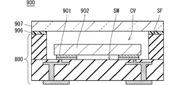
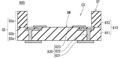
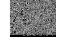
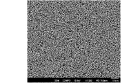
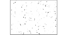
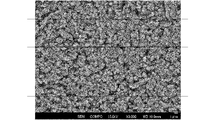
- FIG. 1 It is sectional drawing which shows typically the structure of the electronic apparatus in one Embodiment of this invention. It is sectional drawing which shows the structure of the package of FIG. 1 schematicly. It is an electron micrograph of the mounting surface of the package of the comparative example. It is an electron micrograph of the mounting surface which the package of an Example has. It is an image of the electron micrograph of the fracture surface of the package of the example. It is a figure which shows the image which performed the binarization process with respect to the image of FIG. It is a figure explaining the example of the cutting method which is the method of calculating the average particle diameter from the electron micrograph of the mounting surface which the package of an Example has.
- FIGS. 1 and 2 is a cross-sectional view schematically showing the configuration of the electronic device 900 in the present embodiment and the configuration of the package 800 used for manufacturing the electronic device 900.
- Package 800 (FIG. 2) includes a mounting surface SM on which the electronic component 902 (FIG. 1) is mounted, a cavity CV located on the mounting surface SM, and a lid 907 for sealing the cavity CV. It has a mounting surface SF to be mounted.
- the package 800 has a base portion 810 and a wiring portion 820.
- the base 810 is made of ceramics.
- the ceramic is substantially made of an insulator so that the base 810 can function as an insulating member. As long as this function can be ensured, the ceramics do not necessarily have to be completely made of an insulator. For example, a small amount of non-insulator particles are dispersed in the insulator grains which occupy the majority in volume. May be.
- the base 810 has a cavity CV.
- the base 810 includes a bottom 811 and a frame 812.
- the bottom 811 has a mounting surface SM.
- the mounting surface SM has a mounting surface SM having a size including a rectangle having a long side of 10 mm or more.
- the mounting surface SM is a rectangle having a long side of 10 mm or more.
- the mounting surface SM may have a mounting surface SM having a size including a square having a side of 10 mm or more.
- a rectangle is a kind of square by definition in geometry.
- the frame portion 812 is provided on the bottom portion 811 on the outside of the mounting surface SM so as to surround the cavity CV.
- the frame portion 812 has a fired surface of ceramics as a mounting surface SF.
- the word "fired” (as-fired) means a state in which the surface is not processed as it is sintered. Therefore, the "firing surface” is a surface having a “firing” (as-fired) state. In other words, the "fired surface” means the outer surface of the ceramic product after sintering after sintering. Therefore, the polished surface is not a fired surface.
- the ceramics which is the material of the base portion 810, preferably has an average particle size of 1 ⁇ m or more and 3 ⁇ m or less, more preferably 1.5 ⁇ m or less on the mounting surface SF.
- This average particle size can be calculated from the electron microscope image of the mounting surface SF by using a cutting method. Specifically, a line segment of a known length completely crossing 10 to 50 crystal grains is drawn on a microscope image or a photograph, and this known length is divided by the number of these crystal grains. The average particle size may be calculated by.
- the base portion 810 has a side surface SS extending from the outer edge of the mounting surface SF.
- the side surface SS may have a non-fracture surface SSa and a fracture surface SSb.
- a green laminate in which a plurality of products are arranged is subjected to a half-cut (grooving) treatment with a knife. After firing, each product is individualized by a break process using the portion where the grooving treatment has been performed. In that case, the non-fracture surface SSa becomes an as-fired surface that is fired after being grooved, and has a substantially 0% porosity.
- the fracture surface SSb is a surface that is broken by a break after firing, and preferably has a porosity of 3% or less.
- the side surface SS has a non-fracture surface SSa having substantially no pores and a fracture surface SSb having pores, and the porosity of the latter is preferably 3% or less, more preferably 1.5% or less. Is. This porosity can be calculated by binarizing the image of the electron micrograph of the surface to be evaluated.
- the fracture surface SSb may be located on the side surface of the bottom portion 811 as shown in FIG. 2, and as a modification, it is located on the side surface of the frame portion 812 or on the side surface straddling the bottom portion 811 and the frame portion 812. You can do it.
- the ceramics preferably contain Al 2 O 3 , SiO 2 and Mn O as essential components, and at least one of molybdenum (Mo) atoms and Cr 2 O 3 as optional components.
- the content of Al 2 O 3 is 82.0% by mass or more and 95.0% by mass or less.
- the content of SiO 2 is 3.0% by mass or more and 8.0% by mass or less.
- the content of MnO is 2.0% by mass or more and 6.0% by mass or less.
- the total of the Mo atom content and the Cr 2 O 3 content in terms of MoO 3 is 4.0% by mass or less.
- At least a part of the Mo atom may be contained as Mo oxide. Further, at least a part of Mo atoms may be contained as metal Mo.
- the content of the balance other than the above-mentioned components in the composition of the ceramics is less than 0.1% by mass, more preferably less than 0.05% by mass.
- the wiring portion 820 extends from the cavity CV and penetrates the base portion 810. Specifically, the wiring portion 820 has an external electrode terminal 821 provided outside the cavity CV, an internal wiring 822 penetrating the base portion 810, and an internal electrode terminal 823 facing the cavity CV.
- the internal wiring 822 may be composed of at least one of the internal electrode layer and the via wiring.
- the material of the wiring portion 820 is substantially made of a conductor so that the wiring portion 820 can function as a wiring member. As long as this function can be ensured, the material does not necessarily have to be entirely composed of conductors, for example, a small amount of non-insulator region is dispersed in the conductor region which occupies the majority in volume. You may be.
- the electronic component 902 (FIG. 1) is bonded on the internal electrode terminal 823 by a bonding layer 901. As a result, the electronic component 902 is mounted on the mounting surface SM via the bonding layer 901 and the internal electrode terminal 823.
- the electronic component 902 may have a size including a rectangle having a long side of 10 mm or more, and has a size including, for example, a square having a side of 10 mm or more.
- the electronic component 902 may be a solid-state image sensor.
- the solid-state image sensor is, for example, a CMOS image sensor.
- a CMOS image sensor is particularly excellent as a solid-state image sensor having a large image pickup unit as required for a single-lens reflex camera, some surveillance cameras, an industrial camera, and the like.
- the planar shape of the solid-state image sensor may be a rectangle having a long side of 10 mm or more, or a substantially square shape having a side of 10 mm or more.
- the lid body 907 is mounted on the mounting surface SF of the frame portion 812 via the adhesive layer 906. As a result, the cavity CV of the package 800 is sealed.
- the adhesive layer 906 is made of, for example, a resin adhesive.
- the adhesive layer 906 may be in direct contact with each of the mounting surface SF and the lid 907.
- the electronic component 902 is a solid-state image sensor
- at least a portion of the lid 907 is substantially transparent with respect to the light being imaged, and typically the entire lid 907 is substantially with respect to the light being imaged. Is transparent.
- the wiring portion 820 penetrates the bottom portion 811.
- the wiring portion penetrating between the bottom portion 811 and the frame portion 812 or the wiring portion penetrating the frame portion 812 may be provided.
- a wiring portion to be connected to the electronic component 902 by a bonding wire may be provided.
- the attachment surface SF to which the lid body 907 (FIG. 1) is attached is a fired surface of ceramics.
- dust generation from the mounting surface is suppressed as compared with the case where the mounting surface is a polished surface. Therefore, it is possible to prevent the electronic component 902 from malfunctioning due to foreign matter in the cavity CV.
- FIG. 3 is an electron micrograph of the polished surface as the mounting surface of the package of the comparative example
- FIG. 4 is an electron micrograph of the fired surface as the mounting surface SF of the package of the example.
- the unevenness of the surface state is large as compared with the example, and shedding tends to occur.
- the internal pores are surfaced as defects (holes) by polishing, and foreign substances (ceramics, abrasive grains, etc.) generated during processing and various foreign substances in the process are contained in the defects. Easy to get in. Therefore, there is a risk of dust generation due to the detachment of this foreign matter.
- the polishing process is machining, and due to this, ceramic particles having a low sintering bond force to the surrounding ceramic particles and ceramic particles that are simply attached to the surrounding ceramic particles are generated. Cheap. Therefore, there is a concern that the ceramic particles are easily shed.
- the ceramics of the base 810 have a porosity of 3% or less, particularly 1% or less in the fracture surface SSb, and have an average particle size of 1 ⁇ m or more and 3 ⁇ m or less, particularly 1.5 ⁇ m or less on the mounting surface SF. It is preferable to have. Since the fracture surface SSb is not a fired surface (as-fired surface) unlike the non-fragmented surface SSa and the mounting surface SF, it is usually difficult to set the porosity to 0%. However, it is possible to suppress the porosity to 3% or less, particularly 1% or less, whereby foreign matter is suppressed from being taken into the pores in the cleaning process or the like in manufacturing. Therefore, the risk of dust generation from the pores is reduced.
- the average particle size on the mounting surface SF is 1 ⁇ m or more and 3 ⁇ m or less, particularly 1.5 ⁇ m or less, the denseness can be ensured. As a result, the sintering and bonding force is enhanced, so that the degranulation of the ceramic particles from the mounting surface SF is suppressed. Therefore, the risk of dust generation due to shedding is reduced. From the above, dust generation from the entire base 810 can be suppressed more reliably.
- FIG. 5 is an image of an electron micrograph of the ceramic surface on the fracture surface SSb of the package of the example
- FIG. 6 is a binarization process for the purpose of calculating the average particle size with respect to the image of FIG. It is a figure which shows the image which gave.
- the stomata were observed as areas that were significantly darker than their surroundings. Therefore, as shown in FIG. 6, it was easy to perform the binarization process at a concentration threshold value such that only the above-mentioned dark region is extracted.
- a porosity of 0.98% was obtained by calculating the ratio of the regions extracted in this way.
- FIG. 7 is a diagram illustrating an example of a cutting method which is a method of calculating the average particle size from an electron micrograph of the mounting surface SF of the package of the example.
- the length of the line segment was divided by the number of crystal grains that each line segment crossed. Then, the numerical values obtained by it were averaged with respect to the three line segments. From the above, an average particle size of 1.22 ⁇ m was obtained.
- the electronic component 902 may be a solid-state image sensor having a size including a rectangle having a long side of 10 mm or more. As a result, the size of the image pickup unit of the solid-state image pickup device can be sufficiently secured.
- the ceramics at the base 810 preferably contain Al 2 O 3 , SiO 2 and Mn O as essential components, and at least one of Mo atoms and Cr 2 O 3 as optional components.
- the content of Al 2 O 3 is 82.0% by mass or more and 95.0% by mass or less.
- the content of SiO 2 is 3.0% by mass or more and 8.0% by mass or less.
- the content of MnO is 2.0% by mass or more and 6.0% by mass or less.
- the total of the Mo atom content and the Cr 2 O 3 content in terms of MoO 3 is 4.0% by mass or less.
- the content of the balance is less than 0.1% by mass, more preferably less than 0.05% by mass.
- the ceramics have such a composition, it becomes easy to obtain the dimensional accuracy of the base portion 810 made of the ceramics. Therefore, it becomes easy to secure the flatness of the mounting surface SF without polishing. Further, it becomes easy to secure the parallelism of the mounting surface SF.
- each component is uniformly sintered in a dispersed state without segregation. As a result, dimensional variation of the base 810 is suppressed. Therefore, it becomes easy to secure the flatness of the mounting surface SF without polishing. Further, it becomes easy to secure the parallelism of the mounting surface SF.
- each component is uniformly sintered in a dispersed state without segregation, so that the timing at which the glass component of the base 810 melts is on the side facing the firing setter and on the opposite side. And, it will be almost at the same time. Therefore, it is possible to prevent the base portion 810 from warping in the thickness direction due to this timing shift. Therefore, it becomes easy to secure the flatness and parallelism of the mounting surface SF without polishing.
- the content of the balance is more preferably less than 0.05% by mass. As a result, dimensional variation can be further suppressed.
- the content of the balance is particularly preferably 0% by mass. Thereby, the dimensional variation can be further suppressed.
- the ceramics at the base 810 include a crystalline phase and a glass phase.
- the crystal phase includes not only the Al 2 O 3 crystal phase as the main crystal phase but also the Mo crystal phase as the sub crystal phase.
- the crystal phase may include a crystal phase other than the Al 2 O 3 crystal phase and the Mo crystal phase (hereinafter, referred to as “remaining crystal phase”).
- the main peak intensity of the remainder of the crystalline phase, the main peak intensity of Al 2 O 3 crystal phase 0. It is preferably 5% or less.
- the bending strength of the ceramics can be improved.
- Table 1 below shows the experimental results of investigating the relationship between the composition of the ceramics represented by the composition numbers 1 to 25, the firing temperature suitable for the composition, and the characteristics of the ceramic plate obtained by the composition.
- each raw material powder was mixed at the ratio shown in Table 1 to obtain a mixed powder.
- Polyvinyl butyral, tertiary amine and phthalate ester (diisononyl phthalate: DINP) are mixed as organic components with the obtained mixed powder, and IPA (isopropyl alcohol) and toluene are further mixed as solvents to prepare a slurry. did.
- IPA isopropyl alcohol
- toluene are further mixed as solvents to prepare a slurry.
- a green sheet having a thickness of 50 to 400 ⁇ m was prepared by the doctor blade method.
- the obtained ceramic green sheet was cut into a length of 50 mm and a width of 50 mm, arranged on a firing setter made of Mo, and fired at the firing temperature (maximum temperature) shown in Table 1 above for 2 hours. As a result, 100 ceramic plates having each composition number were produced.
- the dimensional variation of the obtained ceramic plate was measured. Specifically, the external dimensions of the ceramic plate were measured using a dimension measuring device. The mean and standard deviation were calculated. The value obtained by dividing the standard deviation by the average value was defined as the dimensional variation. As a result, among the composition numbers 1 to 25, the dimensional variation of the composition numbers 1 to 17 was small, and the dimensional variation of the composition numbers 1 to 8 and 12 to 17 was particularly small.
- the number of ceramic plates with surface defects caused by sticking to the firing setter during the firing process was counted. As a result, among the composition numbers 1 to 25, the numbers of composition numbers 1 to 17 were small, and the numbers of composition numbers 1 to 5 and 12 to 17 were particularly small.
- the average value of the amount of warpage of the ceramic plate was measured using a three-dimensional shape measuring device. As a result, among the composition numbers 1 to 25, the warpage of the composition numbers 1 to 17 was small, and the warpage of the composition numbers 1 to 9 and 12 to 17 was particularly small.
- the bending strength of the ceramic plate was measured at room temperature according to a three-point bending strength test based on JIS R 1601.
- the relative permittivity of the ceramic plate was measured at room temperature and a frequency of 10 GHz according to the cavity resonance method based on JIS R1641.
- composition numbers 1 to 17 suppressed dimensional variation, sticking to the setter, and warpage as compared with composition numbers 18 to 25. This is because the content of the balance other than Al 2 O 3 , SiO 2 , MnO and the colorant (Mo atom and / and Cr 2 O 3 ) was suppressed to less than 0.1% by mass, so that each component was segregated. It is probable that this was because they were uniformly sintered in a dispersed state. It has been experimentally confirmed that the same result can be obtained even when additives other than MgO, ZrO 2, CaO and BaO are added.
- composition numbers 1 to 9 and 12 to 17 in which the content of the balance was 0.07% by mass or less, the warp was further suppressed. Further, in the compositions Nos. 1 to 8 and 12 to 17 in which the content of the balance was less than 0.05% by mass, the dimensional variation was further suppressed. Further, in the composition numbers 1 to 5 and 12 to 17 in which the content of the balance was 0% by mass, not only the dimensional variation was further suppressed, but also the sticking to the setter was further suppressed.
- composition Nos. 1 to 15 are suitable for ceramic packages requiring strength (for example, those for encapsulating an oscillator or a semiconductor element).
- composition numbers 15 to 17 in which the ratio of the content of SiO 2 to the content of MnO is 1.9 or more and 3.5 or less, the relative permittivity of 8.0 or more and 9.0 or less and the bending resistance of 390 MPa or more are obtained. It was possible to achieve both strength and strength. Therefore, it was found that the composition numbers 15 to 17 are suitable for ceramic packages (for example, those for encapsulating an optical semiconductor element) that require a relatively low relative permittivity.
Landscapes
- Solid State Image Pick-Up Elements (AREA)
Abstract
パッケージ(800)は、電子部品(902)が実装されることになる実装面(SM)と、実装面(SM)上に位置するキャビティ(CV)と、キャビティ(CV)を封止するための蓋体(907)が取り付けられることになる取付面(SF)と、を有している。パッケージ(800)は、セラミックスからなりキャビティ(CV)を有する基部(810)と、基部(810)のキャビティ(CV)から延びて基部(810)を貫通する配線部(820)とを含む。基部(810)は、底部(811)と、枠部(812)とを含む。底部(811)は、10mm以上の長辺を有する長方形を包含する大きさを有する実装面(SM)を有している。枠部(812)は、底部(811)上において実装面(SM)の外側にキャビティ(CV)を囲むように設けられており、取付面(SF)としてセラミックスの焼成面を有している。
Description
本発明は、パッケージに関し、特に、電子部品用のパッケージに関するものである。
特開2006-344838号公報(特許文献1)は固体撮像装置を開示している。固体撮像装置は、凹状のセラミックスパッケージ内に搭載された、撮像素子を有している。パッケージのサイズとしては、10mm四方のサイズが例示されている。撮像素子は、例えば、電荷結合素子(CCD)型または相補型・金属・酸化物・半導体(CMOS)型である。パッケージのサイズが10mm四方であるため、その内部に搭載される撮像素子は、長辺でも10mmよりもかなり小さくなる。パッケージの開口部は透光性窓部材で封止されている。パッケージの窓部材搭載面は、窓部材の密着性およびそれによる気密性を高めるべく、また撮像素子を搭載する際の基準面とするべく、研磨されて平坦化されている。
パッケージに実装される電子部品としては、10mm以上の長辺を有する長方形を包含する大きさを有するものもがある。例えば、高性能の大型カメラ用の固体撮像素子は、小型カメラ用の固体撮像素子に比して、大きな撮像部を構成する必要があり、具体的には10~50mm四方程度の半導体チップとして構成されることが多い。これに対応して、固体撮像素子が実装されるパッケージは、大きな実装面を必要とする。その結果、セラミックスパッケージの焼成収縮差等による反りの影響が、サイズに比して大きくなるため、枠部(封止面)、裏面部(基板への実装面)、キャビティ底部(撮像素子搭載面)の各平面度、および、相互の平行度が乱されやすい。特に取付面の平坦度が低いと、パッケージの取付面と蓋体との間の気密性が低くなってしまう。さらに電子部品が固体撮像素子の場合は、光軸を考慮しなければならないので固体撮像素子と蓋体との平行度も懸念される。そこで従来は取付面の平坦度を、例えば30~50μm程度にまで、研磨によって向上させていた。
しかしながら本発明者らの検討によれば、研磨された取付面からはパッケージのキャビティ内への発塵が生じやすい。この発塵が電子部品の動作に悪影響を及ぼすことがある。特に、電子部品が固体撮像素子の場合は、発塵が画素欠陥を引き起こすことがあり、高性能を求められることが多い大型の固体撮像素子の場合はこの問題は特に深刻である。本発明はこのような課題を解決するためになされたものであり、その目的は、発塵に起因しての電子部品の動作不良を防止することができるパッケージを提供することである。
本発明の一実施の形態におけるパッケージは、電子部品が実装されることになる実装面と、実装面上に位置するキャビティと、キャビティを封止するための蓋体が取り付けられることになる取付面と、を有している。パッケージは、セラミックスからなりキャビティを有する基部と、基部のキャビティから延びて基部を貫通する配線部とを含む。基部は、底部と、枠部とを含む。底部は、10mm以上の長辺を有する長方形を包含する大きさを有する実装面を有している。枠部は、底部上において実装面の外側にキャビティを囲むように設けられており、取付面としてセラミックスの焼成面(as-fired surface)を有している。
本発明の一実施の形態におけるパッケージによれば、蓋体が取り付けられることになる取付面はセラミックスの焼成面である。これにより、取付面が研磨面である場合に比して、取付面からの発塵が抑制される。よって、キャビティ内の異物に起因しての電子部品の動作不良を防止することができる。
この発明の目的、特徴、局面、および利点は、以下の詳細な説明と添付図面とによって、より明白となる。
以下、図面に基づいて本発明の実施の形態について説明する。
図1および図2のそれぞれは、本実施の形態における電子装置900の構成と、電子装置900の製造のために用いられるパッケージ800の構成とを概略的に示す断面図である。
パッケージ800(図2)は、電子部品902(図1)が実装されることになる実装面SMと、実装面SM上に位置するキャビティCVと、キャビティCVを封止するための蓋体907が取り付けられることになる取付面SFとを有している。パッケージ800は、基部810と、配線部820とを有している。
基部810はセラミックスからなる。このセラミックスは、基部810が絶縁部材として機能することができるように、実質的に絶縁体からなる。この機能が確保できる限りにおいてセラミックスは、必ずしも全体が完全に絶縁体からなる必要はなく、例えば、体積的に大多数の割合を占める絶縁体粒の中に、微量の非絶縁体粒が分散されていてもよい。
基部810はキャビティCVを有している。基部810は、底部811と、枠部812とを含む。
底部811は実装面SMを有している。実装面SMは、10mm以上の長辺を有する長方形を包含する大きさを有する実装面SMを有している。例えば、実装面SMは、10mm以上の長辺を有する長方形である。実装面SMは、10mm以上の辺を有する正方形を包含する大きさを有する実装面SMを有していてもよい。なお長方形は、幾何学における定義上、正方形の一種である。
枠部812は、底部811上において、実装面SMの外側に、キャビティCVを囲むように設けられている。枠部812は、取付面SFとしてセラミックスの焼成面を有している。ここで「焼成」(アズファイアード:as-fired)の文言は、焼結したままの、表面加工を行わない状態のことを意味する。よって「焼成面」は、「焼成」(アズファイアード:as-fired)の状態を有する面のことである。言い換えれば、「焼成面」は、焼結後のセラミックス製品の外面(external surface of a ceramic product after sintering)のことを意味する。よって、研磨された表面は焼成面ではない。
基部810の材料である上記セラミックスは取付面SF上において、1μm以上3μm以下、さらに好ましくは1.5μm以下の平均粒子径を有していることが好ましい。この平均粒子径は、取付面SFの電子顕微鏡画像から切断法を用いて算出され得る。具体的には、顕微鏡の映像または写真上で、10~50個の結晶粒を完全に横切る既知の長さの線分が描かれ、この既知の長さをこれら結晶粒の数で割り算することによって平均粒子径が算出されてよい。
基部810は、取付面SFの外縁から延びる側面SSを有している。側面SSは、非破断面SSaと、破断面SSbとを有していてよい。セラミックスパッケージ製品の一般的な製造方法において、複数の製品が配置されたグリーン積層体に、ナイフによるハーフカット(溝加工)処理が施される。焼成後、上記溝加工処理が施されていた箇所を利用してのブレイク工程によって各製品が個片化される。その場合、非破断面SSaは、溝加工された後に焼成された焼成面(as-fired surface)となり、実質的に0%気孔率を有する。破断面SSbは、焼成後にブレイクによって破断された面となり、3%以下の気孔率を有していることが好ましい。言い換えれば、側面SSは、実質的に気孔を有しない非破断面SSaと、気孔を有する破断面SSbとを有し、後者の気孔率は好ましくは3%以下、さらに好ましくは1.5%以下である。この気孔率は、評価される面の電子顕微鏡写真の画像を二値化処理することによって算出され得る。なお破断面SSbは、図2に示されたように底部811の側面上に位置してよく、変形例として、枠部812の側面上、または、底部811および枠部812にまたがる側面上に位置してよい。
上記セラミックスは、好ましくは、Al2O3、SiO2およびMnOを必須成分として含み、モリブデン(Mo)原子およびCr2O3の少なくとも一方を任意成分として含む。Al2O3の含有量は、82.0質量%以上95.0質量%以下である。SiO2の含有量は、3.0質量%以上8.0質量%以下である。MnOの含有量は、2.0質量%以上6.0質量%以下である。MoO3換算でのMo原子の含有量とCr2O3の含有量との合計は、4.0質量%以下である。Mo原子の少なくとも一部は酸化Moとして含まれていてよい。またMo原子の少なくとも一部は金属Moとして含まれていてよい。セラミックスの組成のうち上述した成分以外の残部の含有量は、0.1質量%未満であり、より好ましくは0.05質量%未満である。
配線部820は、キャビティCVから延びて基部810を貫通している。具体的には、配線部820は、キャビティCVの外側に設けられた外部電極端子821と、基部810を貫通する内部配線822と、キャビティCVに面する内部電極端子823とを有している。内部配線822は、内部電極層およびビア配線の少なくともいずれかによって構成され得る。配線部820の材料は、配線部820が配線部材として機能することができるように、実質的に導体からなる。この機能が確保できる限りにおいては、この材料は、必ずしも全体が完全に導体からなる必要はなく、例えば、体積的に大多数の割合を占める導体領域の中に微量の非絶縁体領域が分散されていてもよい。
電子部品902(図1)は、内部電極端子823上に接合層901によって接合されている。これにより電子部品902は、接合層901および内部電極端子823を介して実装面SM上に実装されている。電子部品902は、10mm以上の長辺を有する長方形を包含する大きさを有していてよく、例えば、10mm以上の辺を有する正方形を包含する大きさを有している。電子部品902は固体撮像素子であってよい。固体撮像素子は、例えばCMOSイメージセンサである。一眼レフ、一部の監視用カメラ、および産業用カメラ等に求められるような大きな撮像部を有する固体撮像素子としては、一般に、CMOSイメージセンサが特に優れている。固体撮像素子の平面形状は、10mm以上の長辺を有する長方形であってよく、10mm以上の辺を有する略正方形であってもよい。
蓋体907は枠部812の取付面SF上に接着層906を介して取り付けられている。これによりパッケージ800のキャビティCVが封止されている。接着層906は、例えば樹脂接着剤からなる。接着層906は、取付面SFおよび蓋体907の各々に直接接していてよい。電子部品902が固体撮像素子である場合、蓋体907の少なくとも一部は、撮像される光に関して実質的に透明であり、典型的には蓋体907の全体が、撮像される光に関して実質的に透明である。
なお本実施の形態においては配線部820が底部811を貫通しているが、変形例として、底部811と枠部812との間を貫通する配線部、または、枠部812を貫通する配線部が設けられてもよい。また、変形例として、電子部品902とボンディングワイヤによって接続されることになる配線部が設けられてもよい。
本実施の形態のパッケージ800(図2)によれば、蓋体907(図1)が取り付けられることになる取付面SFはセラミックスの焼成面である。これにより、取付面が研磨面である場合に比して、取付面からの発塵が抑制される。よって、キャビティCV内の異物に起因しての電子部品902の動作不良を防止することができる。
図3は、比較例のパッケージが有する取付面としての研磨面の電子顕微鏡写真であり、図4は、実施例のパッケージが有する取付面SFとしての焼成面の電子顕微鏡写真である。実施例に比して比較例においては、表面状態のむらが大きく、脱粒が生じやすい。また、比較例では、研磨加工によって内部の気孔を欠陥(穴)として表面化させており、この欠陥中へ、加工時に発生する異物(セラミックスや砥粒等)、および、工程内の様々な異物が入りこみやすい。よって、この異物が脱離することに起因しての発塵のおそれがある。また、研磨加工は機械加工であり、これに起因して、周囲のセラミックス粒子への焼結結合力が低いセラミックス粒子、および、周囲のセラミックス粒子に単に付着しているだけのセラミックス粒子を発生させやすい。よって、セラミックス粒子の脱粒が容易に生じることが懸念される。
基部810のセラミックスは、破断面SSbにおいて3%以下、特に1%以下の気孔率を有しており、取付面SF上において1μm以上3μm以下、特に1.5μm以下の平均粒子径を有していることが好ましい。破断面SSbは、非破断面SSaおよび取付面SFと異なり焼成面(as-fired面)ではないので、その気孔率を0%とすることは通常困難である。しかしながら、気孔率を3%以下、特に1%以下に抑えることは可能であり、これにより、製造における洗浄工程等において気孔内に異物が取り込まれることが抑制される。よって、気孔からの発塵のおそれが低減される。また、取付面SF上における平均粒子径が1μm以上3μm以下、特に1.5μm以下であることから、緻密性を確保できる。これにより焼結結合力が高められるので、取付面SFからのセラミックス粒子の脱粒が抑制される。よって、脱粒に起因しての発塵のおそれが低減される。以上から、基部810全体からの発塵を、より確実に抑制することができる。
図5は、実施例のパッケージが有する破断面SSbでのセラミックス表面の電子顕微鏡写真の画像であり、図6は、図5の画像に対して、平均粒子径を算出する目的で二値化処理を施した画像を示す図である。図5に示されているように、気孔が、その周囲に比して際立って濃い領域として観察された。よって、図6に示されているように、おおよそ上記の濃い領域のみが抽出されるような濃度しきい値で二値化処理を行うことは容易であった。本例においては、このようにして抽出された領域の割合を算出することによって、気孔率0.98%を得た。
図7は、実施例のパッケージが有する取付面SFの電子顕微鏡写真から平均粒子径を算出する方法である切断法の例を説明する図である。この例においては、各線分が横切る結晶粒の数によって、線分の長さが割り算された。そして、それによって得られた数値が、3つの線分に関して平均化された。以上により、平均粒子径1.22μmを得た。
電子部品902は、10mm以上の長辺を有する長方形を包含する大きさを有する固体撮像素子であってよい。これにより、固体撮像素子の撮像部の大きさを十分に確保することができる。
基部810のセラミックスは、好ましくは、Al2O3、SiO2およびMnOを必須成分として含み、Mo原子およびCr2O3の少なくとも一方を任意成分として含む。Al2O3の含有量は、82.0質量%以上95.0質量%以下である。SiO2の含有量は、3.0質量%以上8.0質量%以下である。MnOの含有量は、2.0質量%以上6.0質量%以下である。MoO3換算でのMo原子の含有量とCr2O3の含有量との合計は、4.0質量%以下である。残部の含有量は、0.1質量%未満であり、より好ましくは0.05質量%未満である。セラミックスがこのような組成を有することによって、セラミックスからなる基部810の寸法精度を得やすくなる。よって、研磨なしに取付面SFの平坦度を確保しやすくなる。また取付面SFの平行度を確保しやすくなる。
具体的には、上記残部の含有量が0.1質量%未満に抑えられていることから、各成分が、偏析することなく分散された状態で均一に焼結されている。これにより、基部810の寸法ばらつきが抑制される。よって、研磨なしに取付面SFの平坦度を確保しやすくなる。また取付面SFの平行度を確保しやすくなる。
また上記のように、各成分が、偏析することなく分散された状態で均一に焼結されることによって、基部810のガラス成分が溶融するタイミングが、焼成セッターに面する側と、その反対側とで、ほぼ同時となる。よって、このタイミングのずれに起因して基部810が厚み方向において反ることが抑制される。よって、研磨なしに取付面SFの平坦度および平行度を確保しやすくなる。
残部の含有量は、0.05質量%未満がより好ましい。これによって寸法ばらつきをさらに抑制できる。残部の含有量は、0質量%であることが特に好ましい。これによって、寸法ばらつきをさらに抑制できる。
基部810のセラミックスは結晶相とガラス相とを含む。セラミックスが着色剤としてMo原子を含有している場合は、結晶相は、主結晶相としてのAl2O3結晶相に加えて、副結晶相としてのMo結晶相も含む。結晶相は、Al2O3結晶相およびMo結晶相以外の結晶相(以下、「残部の結晶相」という。)を含んでいてもよい。ここで、基部810を粉砕することによって得た試料のX線回折パターンが測定される場合、残部の結晶相のメインピーク強度は、Al2O3結晶相のメインピーク強度に対して、0.5%以下であることが好ましい。これにより、残部の結晶相の存在によりガラス相に歪みが生じることを抑制できる。これにより、セラミックスの曲げ強度(いわゆる、抗折強度)を向上させることができる。
下記の表1は、組成番号1~25で表されたセラミックスの組成と、当該組成に適した焼成温度と、当該組成によって得られたセラミックス板の特性との関係を調べた実験結果を示す。

セラミックス板を作製するために、まず、各原料粉末を表1に示す割合で混合して混合粉末を得た。得られた混合粉末に、ポリビニルブチラール、3級アミンおよびフタル酸エステル(フタル酸ジイソノニル:DINP)を有機成分として混合し、さらに、溶剤としてIPA(イソプロピルアルコール)およびトルエンを混合して、スラリーを調製した。調製したスラリーを用いて、ドクターブレード法にて厚さ50~400μmのグリーンシートを作製した。得られたセラミックスグリーンシートを縦50mm×横50mmにカットし、Mo製の焼成セッター上に並べて、上記表1に示す焼成温度(最高温度)で2時間焼成した。これによって、各組成番号のセラミックス板を100枚ずつ作成した。
得られたセラミックス板の寸法ばらつきを測定した。具体的には、寸法測定装置を用いてセラミックス板の外形寸法を測定した。その平均値および標準偏差を算出した。標準偏差を平均値で割った値を寸法ばらつきとした。結果、組成番号1~25のうち、組成番号1~17の寸法ばらつきが小さく、特に組成番号1~8および12~17の寸法ばらつきがより小さかった。
焼成セッターに焼成工程において貼り付いてしまったことによって表面に欠損が生じたセラミックス板の数を数えた。結果、組成番号1~25のうち、組成番号1~17の数が小さく、特に組成番号1~5および12~17の数が小さかった。
セラミックス板の反り量の平均値を、三次元形状測定器を用いて測定した。結果、組成番号1~25のうち、組成番号1~17の反りが小さく、特に組成番号1~9および12~17の反りが小さかった。
セラミックス板の曲げ強度を、JIS R 1601に準拠した3点曲げ強度試験に従って室温で測定した。またセラミックス板の比誘電率を、JIS R 1641に準拠した空洞共振法に従って、室温、周波数10GHzで測定した。
組成番号1~17では、組成番号18~25に比べて、寸法ばらつき、セッターへの貼り付き、および反りが抑制された。これは、Al2O3、SiO2、MnOおよび着色剤(Mo原子または/およびCr2O3)以外の残部の含有量を0.1質量%未満に抑えたため、各成分が、偏析することなく分散された状態で均一に焼結したため、と考えられる。なお、MgO、ZrO2、CaOおよびBaO以外の添加物を添加した場合においても同様の結果が得られることが実験的に確認されている。
また、残部の含有量を0.07質量%以下とした組成番号1~9および12~17では、反りがさらに抑制された。また、残部の含有量を0.05質量%未満とした組成番号1~8および12~17では、寸法ばらつきがさらに抑制された。また、残部の含有量を0質量%とした組成番号1~5および12~17では、寸法ばらつきがさらに抑制されただけでなく、セッターへの貼り付きもさらに抑制された。
また、MnOの含有量に対するSiO2の含有量の比を0.8以上2.1以下とした組成番号1~15では、曲げ強度が700MPa以上であった。従って組成番号1~15は、強度を要するセラミックスパッケージ(例えば、振動子または半導体素子を封止するもの)に好適であることが分かった。
また、MnOの含有量に対するSiO2の含有量の比を1.9以上3.5以下とした組成番号15~17では、8.0以上9.0以下の比誘電率と390MPa以上の抗折強度とを両立することができた。従って、組成番号15~17は、比較的低い比誘電率を要するセラミックスパッケージ(例えば、光半導体素子を封止するもの)に好適であることが分かった。
この発明は詳細に説明されたが、上記した説明は、すべての局面において、例示であって、この発明がそれに限定されるものではない。例示されていない無数の変形例が、この発明の範囲から外れることなく想定され得るものと解される。
800 パッケージ
810 基部
811 底部
812 枠部
820 配線部
821 外部電極端子
822 内部配線
823 内部電極端子
900 電子装置
901 接合層
902 電子部品
906 接着層
907 蓋体
CV キャビティ
SF 取付面
SM 実装面
810 基部
811 底部
812 枠部
820 配線部
821 外部電極端子
822 内部配線
823 内部電極端子
900 電子装置
901 接合層
902 電子部品
906 接着層
907 蓋体
CV キャビティ
SF 取付面
SM 実装面
Claims (5)
- 電子部品が実装されることになる実装面と、前記実装面上に位置するキャビティと、前記キャビティを封止するための蓋体が取り付けられることになる取付面と、を有するパッケージであって、
セラミックスからなり、前記キャビティを有する基部と、
前記基部の前記キャビティから延びて前記基部を貫通する配線部と、
を備え、
前記基部は、10mm以上の長辺を有する長方形を包含する大きさを有する前記実装面を有する底部と、前記底部上において前記実装面の外側に前記キャビティを囲むように設けられ前記取付面として前記セラミックスの焼成面を有する枠部と、を含む、パッケージ。 - 前記基部は、前記取付面の外縁から延びる側面を有しており、前記側面は破断面を含み、
前記セラミックスは、前記取付面上において1μm以上3μm以下の平均粒子径を有しており、前記破断面において3%以下の気孔率を有している、請求項1に記載のパッケージ。 - 前記電子部品は、10mm以上の長辺を有する長方形を包含する大きさを有する固体撮像素子である、請求項1または2に記載のパッケージ。
- 前記セラミックスは、Al2O3、SiO2およびMnOを必須成分として含み、モリブデン原子およびCr2O3の少なくとも一方を任意成分として含み、
Al2O3の含有量が、82.0質量%以上95.0質量%以下であり、
SiO2の含有量が、3.0質量%以上8.0質量%以下であり、
MnOの含有量が、2.0質量%以上6.0質量%以下であり、
MoO3換算でのモリブデン原子の含有量と、Cr2O3の含有量との合計が、4.0質量%以下であり、
残部の含有量が、0.1質量%未満である、
請求項1から3のいずれか1項に記載のパッケージ。 - 前記セラミックスは、Al2O3、SiO2およびMnOを必須成分として含み、モリブデン原子およびCr2O3の少なくとも一方を任意成分として含み、
Al2O3の含有量が、82.0質量%以上95.0質量%以下であり、
SiO2の含有量が、3.0質量%以上8.0質量%以下であり、
MnOの含有量が、2.0質量%以上6.0質量%以下であり、
MoO3換算でのモリブデン原子の含有量と、Cr2O3の含有量との合計が、4.0質量%以下であり、
残部の含有量が、0.05質量%未満である、
請求項1から3のいずれか1項に記載のパッケージ。
Priority Applications (3)
| Application Number | Priority Date | Filing Date | Title |
|---|---|---|---|
| PCT/JP2019/040287 WO2021070375A1 (ja) | 2019-10-11 | 2019-10-11 | パッケージ |
| JP2021544578A JP7008168B2 (ja) | 2019-10-11 | 2019-10-11 | パッケージ |
| CN201980097998.2A CN114072912B (zh) | 2019-10-11 | 2019-10-11 | 封装体 |
Applications Claiming Priority (1)
| Application Number | Priority Date | Filing Date | Title |
|---|---|---|---|
| PCT/JP2019/040287 WO2021070375A1 (ja) | 2019-10-11 | 2019-10-11 | パッケージ |
Publications (1)
| Publication Number | Publication Date |
|---|---|
| WO2021070375A1 true WO2021070375A1 (ja) | 2021-04-15 |
Family
ID=75437805
Family Applications (1)
| Application Number | Title | Priority Date | Filing Date |
|---|---|---|---|
| PCT/JP2019/040287 Ceased WO2021070375A1 (ja) | 2019-10-11 | 2019-10-11 | パッケージ |
Country Status (3)
| Country | Link |
|---|---|
| JP (1) | JP7008168B2 (ja) |
| CN (1) | CN114072912B (ja) |
| WO (1) | WO2021070375A1 (ja) |
Citations (3)
| Publication number | Priority date | Publication date | Assignee | Title |
|---|---|---|---|---|
| JP2003309226A (ja) * | 2002-02-14 | 2003-10-31 | Kyocera Corp | セラミックパッケージ及びその製造方法 |
| WO2016148217A1 (ja) * | 2015-03-17 | 2016-09-22 | 日本碍子株式会社 | 配線基板 |
| JP2016219616A (ja) * | 2015-05-21 | 2016-12-22 | 京セラ株式会社 | 電子素子実装用基板および電子装置 |
Family Cites Families (4)
| Publication number | Priority date | Publication date | Assignee | Title |
|---|---|---|---|---|
| JP2004228533A (ja) * | 2003-01-27 | 2004-08-12 | Kyocera Corp | セラミックパッケージ |
| CN104347556B (zh) * | 2013-07-23 | 2017-10-10 | 中国振华集团永光电子有限公司 | 二极管封装结构 |
| DE112016001804B4 (de) * | 2015-05-15 | 2021-12-16 | Murata Manufacturing Co., Ltd. | Niedertemperatur-Einbrand-Keramik, keramischer Sinterkörper und elektronisches Keramikbauteil |
| JP6028177B1 (ja) * | 2015-12-25 | 2016-11-16 | 株式会社野田スクリーン | 光源装置 |
-
2019
- 2019-10-11 CN CN201980097998.2A patent/CN114072912B/zh active Active
- 2019-10-11 WO PCT/JP2019/040287 patent/WO2021070375A1/ja not_active Ceased
- 2019-10-11 JP JP2021544578A patent/JP7008168B2/ja active Active
Patent Citations (3)
| Publication number | Priority date | Publication date | Assignee | Title |
|---|---|---|---|---|
| JP2003309226A (ja) * | 2002-02-14 | 2003-10-31 | Kyocera Corp | セラミックパッケージ及びその製造方法 |
| WO2016148217A1 (ja) * | 2015-03-17 | 2016-09-22 | 日本碍子株式会社 | 配線基板 |
| JP2016219616A (ja) * | 2015-05-21 | 2016-12-22 | 京セラ株式会社 | 電子素子実装用基板および電子装置 |
Also Published As
| Publication number | Publication date |
|---|---|
| JP7008168B2 (ja) | 2022-01-25 |
| CN114072912B (zh) | 2024-12-24 |
| CN114072912A (zh) | 2022-02-18 |
| JPWO2021070375A1 (ja) | 2021-12-02 |
Similar Documents
| Publication | Publication Date | Title |
|---|---|---|
| US9872378B2 (en) | Electronic element mounting board and electronic device | |
| CN107001147B (zh) | 陶瓷基体及其制造方法 | |
| JP7008168B2 (ja) | パッケージ | |
| JPWO2014148457A1 (ja) | セラミックパッケージ及び電子部品 | |
| JP2014056127A (ja) | スペーサ、スペーサ集合体、ウェハレベルパッケージ構造体、およびスペーサの製造方法 | |
| JP2023019892A (ja) | 吸着用部材およびその製造方法 | |
| CN106458761A (zh) | 陶瓷基体及其制造方法 | |
| WO2020085148A1 (ja) | セラミック素地 | |
| JPWO2017217490A1 (ja) | セラミック素地及びその製造方法 | |
| JP2012238654A (ja) | 透光性配線基板およびその製造方法 | |
| CN114127935B (zh) | 封装体 | |
| WO2024117149A1 (ja) | 真空チャックおよびその製造方法 | |
| JP6803456B2 (ja) | 配線基板、電子装置用パッケージおよび電子装置 | |
| KR100545133B1 (ko) | 팩키지 구조 및 팩키지 구조를 이용한 센서 모듈 | |
| JP7075499B2 (ja) | 電子線描画装置用枠部材および電子線描画装置 | |
| JP5255476B2 (ja) | セラミック配線基板の製造方法 | |
| JP7789917B2 (ja) | 焼結体 | |
| JP6951134B2 (ja) | 撮像装置用蓋体および撮像装置 | |
| JP2018157074A (ja) | 電子部品、電子部品の製造方法及び電子機器 | |
| JP2017117998A (ja) | 圧電素子およびその製造方法、異物除去ユニットならびに超音波センサ | |
| JP7554285B2 (ja) | パッケージおよびセラミックス基板 | |
| JP2013033798A (ja) | 透光性配線基板 | |
| JP4280096B2 (ja) | フィルタ部材およびこれを用いた固体撮像素子収納用パッケージ | |
| JP2014036368A (ja) | スペーサ、スペーサ集合体、ウェハレベルパッケージ構造体、およびスペーサの製造方法 | |
| JPH04120248U (ja) | 固体撮像素子収納用パツケージ |
Legal Events
| Date | Code | Title | Description |
|---|---|---|---|
| 121 | Ep: the epo has been informed by wipo that ep was designated in this application |
Ref document number: 19948799 Country of ref document: EP Kind code of ref document: A1 |
|
| ENP | Entry into the national phase |
Ref document number: 2021544578 Country of ref document: JP Kind code of ref document: A |
|
| NENP | Non-entry into the national phase |
Ref country code: DE |
|
| 122 | Ep: pct application non-entry in european phase |
Ref document number: 19948799 Country of ref document: EP Kind code of ref document: A1 |