WO2021065866A1 - Terminal material for connectors - Google Patents
Terminal material for connectors Download PDFInfo
- Publication number
- WO2021065866A1 WO2021065866A1 PCT/JP2020/036807 JP2020036807W WO2021065866A1 WO 2021065866 A1 WO2021065866 A1 WO 2021065866A1 JP 2020036807 W JP2020036807 W JP 2020036807W WO 2021065866 A1 WO2021065866 A1 WO 2021065866A1
- Authority
- WO
- WIPO (PCT)
- Prior art keywords
- layer
- intermetallic compound
- plating
- alloy
- less
- Prior art date
Links
- 239000000463 material Substances 0.000 title claims abstract description 72
- 229910017755 Cu-Sn Inorganic materials 0.000 claims abstract description 88
- 229910017927 Cu—Sn Inorganic materials 0.000 claims abstract description 88
- KUNSUQLRTQLHQQ-UHFFFAOYSA-N copper tin Chemical compound [Cu].[Sn] KUNSUQLRTQLHQQ-UHFFFAOYSA-N 0.000 claims abstract description 88
- 229910000765 intermetallic Inorganic materials 0.000 claims abstract description 87
- 239000013078 crystal Substances 0.000 claims abstract description 61
- 229910000881 Cu alloy Inorganic materials 0.000 claims abstract description 17
- 238000001887 electron backscatter diffraction Methods 0.000 claims abstract description 9
- 238000005259 measurement Methods 0.000 claims abstract description 8
- 238000007747 plating Methods 0.000 claims description 77
- 238000010438 heat treatment Methods 0.000 claims description 41
- 238000001816 cooling Methods 0.000 claims description 40
- 238000011282 treatment Methods 0.000 claims description 40
- 229910017482 Cu 6 Sn 5 Inorganic materials 0.000 claims description 26
- 229910052802 copper Inorganic materials 0.000 claims description 19
- 229910052718 tin Inorganic materials 0.000 claims description 19
- 238000000034 method Methods 0.000 claims description 15
- 229910001128 Sn alloy Inorganic materials 0.000 claims description 14
- 229910000990 Ni alloy Inorganic materials 0.000 claims description 11
- 238000004519 manufacturing process Methods 0.000 claims description 8
- 229910052759 nickel Inorganic materials 0.000 claims description 6
- 230000008569 process Effects 0.000 claims description 6
- 150000001875 compounds Chemical class 0.000 claims description 2
- 239000000758 substrate Substances 0.000 abstract description 3
- 239000010410 layer Substances 0.000 description 285
- 239000011135 tin Substances 0.000 description 164
- PXHVJJICTQNCMI-UHFFFAOYSA-N nickel Substances [Ni] PXHVJJICTQNCMI-UHFFFAOYSA-N 0.000 description 94
- 239000010949 copper Substances 0.000 description 89
- 238000009792 diffusion process Methods 0.000 description 24
- 239000002245 particle Substances 0.000 description 20
- 238000005452 bending Methods 0.000 description 14
- 238000001878 scanning electron micrograph Methods 0.000 description 11
- QAOWNCQODCNURD-UHFFFAOYSA-N Sulfuric acid Chemical compound OS(O)(=O)=O QAOWNCQODCNURD-UHFFFAOYSA-N 0.000 description 10
- 238000012360 testing method Methods 0.000 description 6
- 238000009713 electroplating Methods 0.000 description 5
- 239000007788 liquid Substances 0.000 description 5
- 238000002844 melting Methods 0.000 description 5
- 230000008018 melting Effects 0.000 description 5
- 239000000203 mixture Substances 0.000 description 4
- 238000005096 rolling process Methods 0.000 description 4
- RYGMFSIKBFXOCR-UHFFFAOYSA-N Copper Chemical compound [Cu] RYGMFSIKBFXOCR-UHFFFAOYSA-N 0.000 description 3
- 238000004458 analytical method Methods 0.000 description 3
- 230000004888 barrier function Effects 0.000 description 3
- 230000000052 comparative effect Effects 0.000 description 3
- 229910000365 copper sulfate Inorganic materials 0.000 description 3
- ARUVKPQLZAKDPS-UHFFFAOYSA-L copper(II) sulfate Chemical compound [Cu+2].[O-][S+2]([O-])([O-])[O-] ARUVKPQLZAKDPS-UHFFFAOYSA-L 0.000 description 3
- 230000000694 effects Effects 0.000 description 3
- 238000010884 ion-beam technique Methods 0.000 description 3
- 239000002344 surface layer Substances 0.000 description 3
- 229910020836 Sn-Ag Inorganic materials 0.000 description 2
- 229910020988 Sn—Ag Inorganic materials 0.000 description 2
- ATJFFYVFTNAWJD-UHFFFAOYSA-N Tin Chemical compound [Sn] ATJFFYVFTNAWJD-UHFFFAOYSA-N 0.000 description 2
- 239000000654 additive Substances 0.000 description 2
- 230000000996 additive effect Effects 0.000 description 2
- 229910045601 alloy Inorganic materials 0.000 description 2
- 239000000956 alloy Substances 0.000 description 2
- 239000010953 base metal Substances 0.000 description 2
- KGBXLFKZBHKPEV-UHFFFAOYSA-N boric acid Chemical compound OB(O)O KGBXLFKZBHKPEV-UHFFFAOYSA-N 0.000 description 2
- 239000011247 coating layer Substances 0.000 description 2
- 238000009429 electrical wiring Methods 0.000 description 2
- 238000011156 evaluation Methods 0.000 description 2
- 238000000605 extraction Methods 0.000 description 2
- 238000003780 insertion Methods 0.000 description 2
- 230000037431 insertion Effects 0.000 description 2
- QMMRZOWCJAIUJA-UHFFFAOYSA-L nickel dichloride Chemical compound Cl[Ni]Cl QMMRZOWCJAIUJA-UHFFFAOYSA-L 0.000 description 2
- LGQLOGILCSXPEA-UHFFFAOYSA-L nickel sulfate Chemical compound [Ni+2].[O-]S([O-])(=O)=O LGQLOGILCSXPEA-UHFFFAOYSA-L 0.000 description 2
- 229910000363 nickel(II) sulfate Inorganic materials 0.000 description 2
- 238000012545 processing Methods 0.000 description 2
- 229910021586 Nickel(II) chloride Inorganic materials 0.000 description 1
- 241000080590 Niso Species 0.000 description 1
- 230000015572 biosynthetic process Effects 0.000 description 1
- 239000004327 boric acid Substances 0.000 description 1
- 238000004364 calculation method Methods 0.000 description 1
- 230000008859 change Effects 0.000 description 1
- 230000006866 deterioration Effects 0.000 description 1
- 238000007772 electroless plating Methods 0.000 description 1
- 238000010894 electron beam technology Methods 0.000 description 1
- 230000001771 impaired effect Effects 0.000 description 1
- 150000002500 ions Chemical class 0.000 description 1
- 238000000691 measurement method Methods 0.000 description 1
- 239000002184 metal Substances 0.000 description 1
- 229910052751 metal Inorganic materials 0.000 description 1
- 239000007769 metal material Substances 0.000 description 1
- 230000003287 optical effect Effects 0.000 description 1
- 230000003647 oxidation Effects 0.000 description 1
- 238000007254 oxidation reaction Methods 0.000 description 1
- 230000037361 pathway Effects 0.000 description 1
- 238000010791 quenching Methods 0.000 description 1
- 230000000171 quenching effect Effects 0.000 description 1
- RCIVOBGSMSSVTR-UHFFFAOYSA-L stannous sulfate Chemical compound [SnH2+2].[O-]S([O-])(=O)=O RCIVOBGSMSSVTR-UHFFFAOYSA-L 0.000 description 1
- 238000010998 test method Methods 0.000 description 1
- FAKFSJNVVCGEEI-UHFFFAOYSA-J tin(4+);disulfate Chemical compound [Sn+4].[O-]S([O-])(=O)=O.[O-]S([O-])(=O)=O FAKFSJNVVCGEEI-UHFFFAOYSA-J 0.000 description 1
- 229910000375 tin(II) sulfate Inorganic materials 0.000 description 1
Images


Classifications
-
- C—CHEMISTRY; METALLURGY
- C25—ELECTROLYTIC OR ELECTROPHORETIC PROCESSES; APPARATUS THEREFOR
- C25D—PROCESSES FOR THE ELECTROLYTIC OR ELECTROPHORETIC PRODUCTION OF COATINGS; ELECTROFORMING; APPARATUS THEREFOR
- C25D5/00—Electroplating characterised by the process; Pretreatment or after-treatment of workpieces
- C25D5/16—Electroplating with layers of varying thickness
-
- C—CHEMISTRY; METALLURGY
- C25—ELECTROLYTIC OR ELECTROPHORETIC PROCESSES; APPARATUS THEREFOR
- C25D—PROCESSES FOR THE ELECTROLYTIC OR ELECTROPHORETIC PRODUCTION OF COATINGS; ELECTROFORMING; APPARATUS THEREFOR
- C25D3/00—Electroplating: Baths therefor
- C25D3/02—Electroplating: Baths therefor from solutions
- C25D3/12—Electroplating: Baths therefor from solutions of nickel or cobalt
-
- C—CHEMISTRY; METALLURGY
- C25—ELECTROLYTIC OR ELECTROPHORETIC PROCESSES; APPARATUS THEREFOR
- C25D—PROCESSES FOR THE ELECTROLYTIC OR ELECTROPHORETIC PRODUCTION OF COATINGS; ELECTROFORMING; APPARATUS THEREFOR
- C25D3/00—Electroplating: Baths therefor
- C25D3/02—Electroplating: Baths therefor from solutions
- C25D3/30—Electroplating: Baths therefor from solutions of tin
-
- C—CHEMISTRY; METALLURGY
- C25—ELECTROLYTIC OR ELECTROPHORETIC PROCESSES; APPARATUS THEREFOR
- C25D—PROCESSES FOR THE ELECTROLYTIC OR ELECTROPHORETIC PRODUCTION OF COATINGS; ELECTROFORMING; APPARATUS THEREFOR
- C25D3/00—Electroplating: Baths therefor
- C25D3/02—Electroplating: Baths therefor from solutions
- C25D3/38—Electroplating: Baths therefor from solutions of copper
-
- C—CHEMISTRY; METALLURGY
- C25—ELECTROLYTIC OR ELECTROPHORETIC PROCESSES; APPARATUS THEREFOR
- C25D—PROCESSES FOR THE ELECTROLYTIC OR ELECTROPHORETIC PRODUCTION OF COATINGS; ELECTROFORMING; APPARATUS THEREFOR
- C25D5/00—Electroplating characterised by the process; Pretreatment or after-treatment of workpieces
- C25D5/10—Electroplating with more than one layer of the same or of different metals
- C25D5/12—Electroplating with more than one layer of the same or of different metals at least one layer being of nickel or chromium
- C25D5/14—Electroplating with more than one layer of the same or of different metals at least one layer being of nickel or chromium two or more layers being of nickel or chromium, e.g. duplex or triplex layers
-
- C—CHEMISTRY; METALLURGY
- C25—ELECTROLYTIC OR ELECTROPHORETIC PROCESSES; APPARATUS THEREFOR
- C25D—PROCESSES FOR THE ELECTROLYTIC OR ELECTROPHORETIC PRODUCTION OF COATINGS; ELECTROFORMING; APPARATUS THEREFOR
- C25D5/00—Electroplating characterised by the process; Pretreatment or after-treatment of workpieces
- C25D5/48—After-treatment of electroplated surfaces
- C25D5/50—After-treatment of electroplated surfaces by heat-treatment
- C25D5/505—After-treatment of electroplated surfaces by heat-treatment of electroplated tin coatings, e.g. by melting
-
- C—CHEMISTRY; METALLURGY
- C25—ELECTROLYTIC OR ELECTROPHORETIC PROCESSES; APPARATUS THEREFOR
- C25D—PROCESSES FOR THE ELECTROLYTIC OR ELECTROPHORETIC PRODUCTION OF COATINGS; ELECTROFORMING; APPARATUS THEREFOR
- C25D5/00—Electroplating characterised by the process; Pretreatment or after-treatment of workpieces
- C25D5/60—Electroplating characterised by the structure or texture of the layers
- C25D5/615—Microstructure of the layers, e.g. mixed structure
- C25D5/617—Crystalline layers
-
- C—CHEMISTRY; METALLURGY
- C25—ELECTROLYTIC OR ELECTROPHORETIC PROCESSES; APPARATUS THEREFOR
- C25D—PROCESSES FOR THE ELECTROLYTIC OR ELECTROPHORETIC PRODUCTION OF COATINGS; ELECTROFORMING; APPARATUS THEREFOR
- C25D7/00—Electroplating characterised by the article coated
-
- H—ELECTRICITY
- H01—ELECTRIC ELEMENTS
- H01R—ELECTRICALLY-CONDUCTIVE CONNECTIONS; STRUCTURAL ASSOCIATIONS OF A PLURALITY OF MUTUALLY-INSULATED ELECTRICAL CONNECTING ELEMENTS; COUPLING DEVICES; CURRENT COLLECTORS
- H01R13/00—Details of coupling devices of the kinds covered by groups H01R12/70 or H01R24/00 - H01R33/00
- H01R13/02—Contact members
- H01R13/03—Contact members characterised by the material, e.g. plating, or coating materials
-
- C—CHEMISTRY; METALLURGY
- C22—METALLURGY; FERROUS OR NON-FERROUS ALLOYS; TREATMENT OF ALLOYS OR NON-FERROUS METALS
- C22C—ALLOYS
- C22C9/00—Alloys based on copper
Definitions
- the present invention relates to a connector terminal material used for connecting electrical wiring of automobiles, consumer devices, and the like.
- the present application claims priority based on Japanese Patent Application No. 2019-181011 filed on September 30, 2019, the contents of which are incorporated herein by reference.
- Terminal materials for connectors used for connecting electrical wiring in automobiles and consumer equipment are generally reflow tin obtained by heating, melting, and solidifying a Sn plating film formed by electrolytic plating on the surface of a base material made of Cu or Cu alloy. Manufactured using plating materials.
- terminal materials are often used in high temperature environments such as engine rooms, or in environments where the terminals themselves generate heat due to energization with a large current.
- Cu that has diffused outward from the base metal reacts with the Sn layer and grows to the surface as a Cu-Sn intermetallic compound, and the Cu is oxidized to increase the contact resistance. This has become a problem, and there is a demand for terminal materials that maintain stable electrical connection reliability for a long time even in a high temperature environment.
- Patent Document 1 on the surface of a base material made of Cu or Cu alloy, a Ni layer, an intermediate layer made of a Cu—Sn alloy layer (Cu—Sn intermetallic compound layer), and a surface layer made of Sn or Sn alloy are formed. Terminal materials formed in this order are disclosed.
- the Ni layer is epitaxially grown on the substrate, the average crystal grain size of the Ni layer is 1 ⁇ m or more, the thickness of the Ni layer is 0.1 to 1.0 ⁇ m, and the thickness of the intermediate layer is 0.2.
- the surface layer thickness By setting the surface layer thickness to 0.5 to 2.0 ⁇ m to 1.0 ⁇ m, the barrier property to the base material made of Cu or Cu alloy is enhanced, and the diffusion of Cu is more reliably prevented to provide heat resistance.
- a Sn plating material capable of maintaining stable contact resistance even in a high temperature environment has been obtained.
- a Ni or Ni alloy layer having a thickness of 0.05 to 1.0 ⁇ m is formed on the surface of a base material made of copper or a copper alloy, and a Sn or Sn alloy layer is formed on the outermost surface side.
- a terminal material in which one or more diffusion layers containing Cu and Sn as main components or diffusion layers containing Cu, Ni and Sn as main components are formed between a Ni or Ni alloy layer and a Sn or Sn alloy layer. ing. Further, among these diffusion layers, the thickness of the diffusion layer in contact with the Sn or Sn alloy layer is 0.2 to 2.0 ⁇ m, the Cu content is 50% by weight or less, and the Ni content is 20% by weight or less. It is described as.
- Patent Document 3 describes a Sn-based plating layer having a plurality of plating layers on the surface of a Cu-based base material and made of a Sn or Sn alloy having an average thickness of 0.05 to 1.5 ⁇ m constituting the surface layer portion thereof. Discloses a terminal material on which a Sn—Ag coating layer having a hardness of 10 to 20 Hv and an average thickness of 0.05 to 0.5 ⁇ m is formed. Further, it is described that the Sn—Ag coating layer contains Sn particles and Ag 3 Sn particles, the average particle size of the Sn particles is 1 to 10 ⁇ m, and the average particle size of the Ag 3 Sn particles is 10 to 100 nm. There is.
- the Ni layer covering the surface of the base material suppresses the diffusion of Cu from the base material, and the Cu-Sn intermetallic compound layer above it diffuses Ni into the Sn layer.
- This effect can maintain stable electrical connection reliability for a long time in a high temperature environment.
- Ni diffuses into the Sn layer under a high temperature environment, which damages a part of the Ni layer, and Cu of the base material diffuses from the damaged portion to the Sn layer to reach the surface and oxidize. There is a problem that the contact resistance increases due to this.
- the present invention has been made in view of the above circumstances, and an object of the present invention is to improve the heat resistance of a terminal material in which a Ni layer, a Cu-Sn intermetallic compound layer, and a Sn layer are sequentially formed.
- the present inventor has diligently researched a solution to the above-mentioned problems in a terminal material in which a Ni layer, a Cu-Sn intermetallic compound layer, and a Sn layer are sequentially formed on the surface of a base material made of Cu or a Cu alloy. I found the findings of.
- the Cu-Su intermetallic compound layer functions as a diffusion barrier for Ni, it was considered to lengthen the reflow time to make the Cu-Su intermetallic compound layer thicker, but Sn is consumed by that amount. As a result, the Sn layer becomes thin, which eventually leads to a decrease in heat resistance, which is not suitable as a solution.
- the Cu-Sn intermetallic compound layer between the Ni layer and the Sn layer has an uneven interface with the Sn layer. That is, a large number of island-shaped portions projecting toward the Sn layer are connected, and the Cu-Sn intermetallic compound layer has locally thick and thin portions. It was confirmed that the Ni layer was damaged by the diffusion of Ni into the Sn layer in the thin portion, and the Cu of the base material diffused into the Sn layer from the damaged portion.
- the thin portion of the Cu-Sn intermetallic compound layer is formed in a portion where the growth of the Cu-Sn intermetallic compound is locally likely to proceed and a portion in which the growth of the Cu-Sn intermetallic compound is difficult to proceed locally in the Sn layer formed on the thin portion. It is considered that the existence of is a factor. Therefore, it is important to grow the Cu—Sn alloy layer as flat as possible so that this locally thin portion does not occur, and for this reason, it is necessary to form as many Cu diffusion paths as possible in the Sn layer. We obtained the finding that it is effective. Based on such knowledge, the present invention has the following configuration.
- the terminal material for a connector of the present invention is formed on a base material whose surface is at least made of Cu or a Cu alloy and the base material, and is formed on a Ni layer made of Ni or a Ni alloy and the Ni layer. It has a Cu-Sn intermetallic compound layer having Cu 6 Sn 5 and a Sn layer formed on the Cu-Sn intermetallic compound layer and made of Sn or a Sn alloy.
- the thickness of the Ni layer is 0.1 ⁇ m or more and 1.0 ⁇ m or less
- the thickness of the Cu-Sn intermetallic compound layer is 0.2 ⁇ m or more, preferably 0.3 ⁇ m or more, and further.
- the thickness of the Sn layer is preferably 0.4 ⁇ m or more and 2.5 ⁇ m or less, preferably 2.0 ⁇ m or less, and the thickness of the Sn layer is 0.5 ⁇ m or more, preferably 0.8 ⁇ m or more, still more preferably 1.0 ⁇ m or more, and It is 3.0 ⁇ m or less, preferably 2.5 ⁇ m or less, and more preferably 2.0 ⁇ m or less.
- the cross sections of the Cu-Sn intermetallic compound layer and the Sn layer are analyzed by the EBSD method in a measurement step of 0.1 ⁇ m, and the boundary where the orientation difference between adjacent pixels is 2 ° or more is regarded as a grain boundary.
- the average crystal grain size of Cu 6 Sn 5 in the Cu-Sn intermetallic compound layer is Dc and the average crystal grain size of the Sn layer is Ds
- the average crystal grain size Dc is 0.5 ⁇ m or more
- the grains are grains.
- the diameter ratio Ds / Dc is 5 or less.
- the average crystal grain size Dc of Cu 6 Sn 5 in the Cu-Sn intermetallic compound layer is increased to 0.5 ⁇ m or more, that is, the crystal grain boundary of Cu 6 Sn 5 is reduced.
- the number of thin parts of the Cu-Sn intermetallic compound layer is reduced, and the starting point of damage to the Ni layer is reduced.
- the Cu-Sn intermetallic layer is formed.
- the grain boundaries of the Sn layer with respect to the crystals of Cu 6 Sn 5 in the compound layer are increased, the diffusion path of Cu into the Sn layer is increased, and the thickness of the Cu-Sn intermetallic compound layer is closer to uniform than before. Can grow.
- the thickness of the Ni layer is less than 0.1 ⁇ m, the effect of preventing the diffusion of Cu from the base material is poor, and if it exceeds 1.0 ⁇ m, cracks may occur due to bending or the like.
- the thickness of the Cu-Sn intermetallic compound layer is less than 0.2 ⁇ m, the diffusion of Ni into the Sn layer may not be sufficiently suppressed in a high temperature environment, and if it exceeds 2.5 ⁇ m, the Sn layer becomes Cu—. It becomes thin due to consumption due to excessive formation of the Sn intermetallic compound layer, and the heat resistance is lowered.
- the thickness of the Sn layer is less than 0.5 ⁇ m, the Cu-Sn intermetallic compound is likely to be exposed on the surface at a high temperature, and the Cu-Sn intermetallic compound is easily oxidized to form an oxide of Cu. Resistance increases. On the other hand, if the thickness of the Sn layer exceeds 3.0 ⁇ m, the insertion / extraction force during use of the connector tends to increase.
- the Cu is formed on the Cu 3 Sn layer It is composed of 6 Sn 5 layers, and the coverage of the Cu 3 Sn layer with respect to the Ni layer is 20% or more, preferably 25% or more, and more preferably 30% or more.
- Cu-Sn intermetallic compound layer is a two-layer structure of the Cu 3 Sn layer and the Cu 6 Sn 5 layer by Cu 3 Sn layer constituting the lower layer covering the Ni layer, maintain the integrity of the Ni layer Therefore, it is possible to prevent the diffusion of Cu in the base material and suppress an increase in contact resistance and the like.
- the coverage of the Cu 3 Sn layer is preferably 20% or more.
- the Sn layer has a grain boundary length of a crystal having an orientation difference of 15 ° or more among the crystal grain boundaries defined by the EBSD method as La, and the orientation difference is La. Assuming that the grain boundary length of the crystal of 2 ° or more and less than 15 ° is Lb, the ratio of Lb (Lb / (Lb + La)) to the total La + Lb of these grain boundary lengths is 0.1 or more.
- This Lb ratio (Lb / (Lb + La)) is the ratio of the length occupied by the grain boundaries with a small orientation difference. By increasing this ratio, the number of fine Sn crystals increases. That is, since the grain boundaries of Sn, which is the diffusion path of Cu into the Sn layer, increase, the thickness of the Cu-Sn intermetallic compound layer becomes more uniform.
- the method for producing a terminal material for a connector of the present invention includes a Ni plating process for forming a plating layer made of Ni or Ni alloy on the surface of a base material whose surface is made of Cu or Cu alloy at least, and a plating layer made of Cu or Cu alloy. It has a Cu plating treatment for forming the above, a plating treatment step for forming a Sn or Sn alloy plating layer in this order, and a reflow treatment step for reflowing after the plating treatment step. By these steps, a Ni layer made of Ni or a Ni alloy is formed on the base material, and a Cu-Sn intermetallic compound made of Cu and Sn intermetallic compound (IMC: Intermetallic Copper) is formed on the Ni layer.
- IMC Intermetallic Copper
- a terminal material for a connector is produced in which a layer is formed and a Sn layer made of Sn or a Sn alloy is formed on the Cu-Sn intermetallic compound layer.
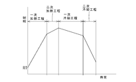
- the reflow treatment includes a primary heat treatment of heating to 240 ° C. or higher at a heating rate of 20 ° C./sec or higher and 75 ° C./sec or lower, and 240 ° C. or higher and 300 ° C. or lower after the primary heat treatment.
- the particle size of the Sn layer is finely controlled by the secondary cooling step from the vicinity of the melting point (about 232 ° C.) of Sn.
- the particle size of the Sn layer can be controlled by the start temperature and the cooling rate of the secondary cooling step.
- the structure of the Sn layer can be made into a solidified structure.
- the internal stress of the Sn layer can be released and the generation of whiskers can be suppressed.
- the present invention it is possible to improve the heat resistance of a terminal material in which a Ni layer, a Cu-Sn intermetallic compound layer, and a Sn layer are sequentially formed.
- FIG. 1 It is sectional drawing which shows one Embodiment of the terminal material for a connector which concerns on this invention in a schematic form. It is a temperature profile which graphed the relationship between the temperature and time of the reflow condition at the time of manufacturing the terminal material for a connector of FIG. It is an SEM image of the film cross section of the sample A27 after holding at 145 ° C. ⁇ 240 hours. It is a surface SEM image of the Ni layer of the sample A27 observed by peeling off the Sn layer and the Cu—Sn intermetallic compound layer after holding at 145 ° C. for 240 hours. It is a Ni layer surface SEM image of the sample B2 after holding at 145 ° C. ⁇ 240 hours. It is a Ni layer surface SEM image of the sample A48 after holding at 145 ° C. ⁇ 240 hours.
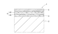
- a Ni layer 3 made of Ni or a Ni alloy is formed on a base material 2 whose surface is at least made of Cu or a Cu alloy, and the Ni layer is formed.
- a Cu-Sn intermetallic compound layer 4 made of a Cu and Sn intermetallic compound is formed on the Cu-Sn intermetallic compound layer 4, and a Sn layer 5 made of a Sn or Sn alloy is formed on the Cu-Sn intermetallic compound layer 4.
- the base material 2 is a strip-shaped strip, and its composition is not particularly limited as long as the surface is made of Cu or a Cu alloy.
- the Ni layer 3 is formed by electroplating Ni or a Ni alloy on the surface of the base material 2, and is formed to have a thickness of 0.1 ⁇ m or more and 1.0 ⁇ m or less. If the thickness of the Ni layer 3 is less than 0.1 ⁇ m, the effect of preventing the diffusion of Cu from the base material 2 is poor, and if it exceeds 1.0 ⁇ m, cracks may occur due to bending or the like.
- the Cu-Sn intermetallic compound layer 4 is a Cu plating treatment for forming a plating layer made of Cu or a Cu alloy on the Ni layer 3, and Sn plating for forming a plating layer made of Sn or a Sn alloy. It is formed by reacting Cu and Sn by performing the treatments in this order and then performing the reflow treatment.
- the Cu-Sn intermetallic compound layer 4 has a two-layer structure of a Cu 3 Sn layer 41 formed on the Ni layer 3 and a Cu 6 Sn 5 layer 42 arranged on the Cu 3 Sn layer. However, it is formed to have a thickness of 0.2 ⁇ m or more and 2.5 ⁇ m or less. The coverage of the Cu 3 Sn layer with respect to the Ni layer 3 is 20% or more.
- the thickness of the Cu-Sn intermetallic compound layer 4 is less than 0.2 ⁇ m, the function of Cu as a diffusion barrier is impaired, and the contact resistance may increase in a high temperature environment. If the thickness exceeds 2.5 ⁇ m, the Sn layer 5 is consumed more and the Sn layer 5 becomes thinner, resulting in a decrease in heat resistance.
- the thickness of the Cu-Sn intermetallic compound layer 4 is preferably 0.3 ⁇ m or more, more preferably 0.4 ⁇ m or more, and preferably 2.0 ⁇ m or less.
- the Ni layer 3 By covering the Ni layer 3 with the Cu 3 Sn layer 41, it is possible to maintain the soundness of the Ni layer 3, prevent the diffusion of Cu in the base material 2, and suppress an increase in contact resistance and the like.
- the coverage of the Cu 3 Sn layer 41 is preferably 20% or more.
- the coverage of the Cu 3 Sn layer 41 is preferably 25% or more, more preferably 30% or more.
- the Cu 3 Sn layer 41 does not always cover the entire surface of the Ni layer 3, and there may be a portion on the Ni layer 3 in which the Cu 3 Sn layer 41 is not formed. In that case, , The Cu 6 Sn 5 layer 42 is in direct contact with the Ni layer 3.
- the film portion of the terminal material is cross-processed with a focused ion beam (FIB), the cross section of the film is observed with a scanning electron microscope (SEM), and the Ni layer 3 and Cu-Sn are observed. It is determined by the ratio of the interface length of the Cu 3 Sn layer in contact with the Ni layer 3 to the interface length of the metal-to-metal compound layer 4.
- FIB focused ion beam
- SEM scanning electron microscope
- the Sn layer 5 is formed by subjecting the Ni layer 3 to a Cu plating treatment and a Sn plating treatment, and then a reflow treatment.
- the thickness of the Sn layer 5 is 0.5 ⁇ m or more and 3.0 ⁇ m or less. If the thickness of the Sn layer 5 is less than 0.5 ⁇ m, the Cu-Sn intermetallic compound is likely to be exposed on the surface at a high temperature, and the Cu-Sn intermetallic compound is easily oxidized to form an oxide of Cu on the surface. Therefore, the contact resistance increases. On the other hand, if the thickness of the Sn layer 5 exceeds 3.0 ⁇ m, the insertion / extraction force during use of the connector tends to increase.
- the thickness of the Sn layer 5 is preferably 0.8 ⁇ m or more, more preferably 1.0 ⁇ m or more, preferably 2.5 ⁇ m or less, still more preferably 2.0 ⁇ m or less.
- the cross sections of the Cu-Sn intermetallic compound layer 4 and the Sn layer 5 are analyzed by the EBSD method in a measurement step of 0.1 ⁇ m, and the boundary where the orientation difference between adjacent pixels is 2 ° or more is regarded as a grain boundary.
- the average crystal grain size of the Cu-Sn intermetallic compound layer 4 is Dc and the average crystal grain size of the Sn layer 5 is Ds
- the average crystal grain size Dc is 0.5 ⁇ m or more
- the particle size ratio Ds / Dc is high. It is 5 or less.
- the average crystal grain size Dc of the Cu-Sn intermetallic compound layer 4 By increasing the average crystal grain size Dc of the Cu-Sn intermetallic compound layer 4 to 0.5 ⁇ m or more, the unevenness of the Cu-Sn intermetallic compound layer 4 is reduced, and the occurrence of locally too thin portions is reduced. be able to. Further, by setting the ratio (Ds / Dc) of the average crystal grain size Ds of the Sn layer 5 to the average crystal grain size Dc of the Cu-Sn intermetallic compound layer 4 to 5 or less, the Cu-Sn intermetallic compound layer 4 can be formed. The grain boundaries of the Sn layer 5 with respect to the crystal are increased, the diffusion path of Cu into the Sn layer 5 is increased, and the Cu-Sn intermetallic compound layer 4 can be grown with a uniform thickness.
- the average crystal particle size Dc is preferably 0.6 ⁇ m or more, and the particle size ratio Ds / Dc is preferably 4 or less, more preferably 3 or less.
- the grain boundary length of the crystal having an orientation difference of 15 ° or more is La, and the grain of the crystal having an orientation difference of 2 ° or more and less than 15 °.
- the boundary length is Lb
- the Lb ratio (Lb / (Lb + La)) is 0.1 or more.
- This Lb ratio (Lb / (Lb + La)) is the ratio of the length occupied by the grain boundaries with a small orientation difference, and increasing the LB ratio increases the number of fine Sn crystals. That is, since the grain boundaries of Sn, which is the diffusion path of Cu into the Sn layer 5, increase, the thickness of the Cu-Sn intermetallic compound layer 4 becomes more uniform.
- the Lb ratio is preferably 0.2 or more, more preferably 0.3 or more.
- the terminal material 1 for a connector configured in this way has a Ni plating process for forming a plating layer made of Ni or a Ni alloy on the base material 2, a Cu plating process for forming a plating layer made of Cu or a Cu alloy, Sn or It is formed by performing Sn plating treatment for forming a plating layer made of Sn alloy in order and then reflowing treatment.
- Ni plating treatment a general Ni plating bath may be used.
- a watt bath containing nickel sulfate (NiSO 4 ), nickel chloride (NiCl 2 ), and boric acid (H 3 BO 3 ) as main components can be used. ..
- the temperature of the plating bath is 20 ° C. or higher and 60 ° C. or lower, and the current density is 5 to 60 A / dm 2 or lower.
- the film thickness of the Ni plating layer formed by this Ni plating treatment is 0.1 ⁇ m or more and 1.0 ⁇ m or less.
- a general Cu plating bath may be used.
- a copper sulfate bath containing copper sulfate (CuSO 4 ) and sulfuric acid (H 2 SO 4 ) as main components can be used.
- the temperature of the plating bath is 20 to 50 ° C., and the current density is 1 to 50 A / dm 2 .
- the film thickness of the Cu plating layer formed by this Cu plating treatment is 0.05 ⁇ m or more and 10 ⁇ m or less.
- a general Sn plating bath may be used.
- a sulfuric acid bath containing sulfuric acid (H 2 SO 4 ) and stannous sulfate (Sn SO 4 ) as main components can be used.
- the temperature of the plating bath is 15 to 35 ° C., and the current density is 1 to 30 A / dm 2 .
- the film thickness of the Cu plating layer formed by this Sn plating treatment is 0.1 ⁇ m or more and 5.0 ⁇ m or less.
- the Cu plating layer and the Sn plating layer are heated to melt them once and then rapidly cooled.
- primary heating in which the treated material after the Cu plating treatment and the Sn plating treatment is heated to 240 ° C. or higher at a heating rate of 20 ° C./sec or higher and 75 ° C./sec or lower in a heating furnace in a CO-reducing atmosphere.
- a cooling step and a secondary cooling step of cooling at a cooling rate of 100 ° C./sec or more and 300 ° C./sec or less after the primary cooling step are performed.
- the temperature may be maintained at the temperature reached by the primary heat treatment, or after heating to a temperature lower than the target temperature by the primary heat treatment, the temperature is gradually reached to the target temperature by the secondary heat treatment. It may be raised, or it may be appropriately changed within the above temperature range.
- FIG. 2 shows an example of the relationship between temperature and time in the reflow process.
- a connector terminal material 1 in which a Cu—Sn intermetallic compound layer 4 and a Sn layer 5 are sequentially formed on the Ni layer 3 is obtained.
- the Cu-Sn intermetallic compound layer 4 is mainly composed of a Cu 3 Sn layer 41 and a Cu 6 Sn 5 layer 42. A part of the Cu plating layer may remain between the Ni layer 3 and the Cu—Sn intermetallic compound layer 4.
- the process of slowly cooling to near the melting point of Sn in the primary cooling step and quenching in the subsequent secondary cooling step is preferable.
- Sn is heated to a temperature equal to or higher than the melting point, and by adjusting the conditions of primary heating and secondary heating, Cu and Sn are sufficiently reacted to increase the particle size of the Cu-Sn intermetallic compound. Grow. Then, after a primary cooling step of gradual cooling, the particle size of the Sn layer 5 is finely controlled by a secondary cooling step from the vicinity of the melting point of Sn. The particle size of the Sn layer 5 can be controlled by the start temperature and the cooling rate of the secondary cooling step. Further, by heat treatment in this way, the Sn layer 5 can be formed into a solidified structure.
- This connector terminal material 1 is press-punched to a predetermined outer shape, subjected to mechanical processing such as bending, and molded into a male terminal or a female terminal.
- the Cu-Sn intermetallic compound layer 4 has few parts that are locally thinned, and the Cu-Sn intermetallic compound layer 4 grows with a thickness closer to uniform, and the Ni layer 3 is grown even in a high temperature environment. Since damage is suppressed, low contact resistance can be maintained and excellent heat resistance can be exhibited.
- the Ni plating layer, the Cu plating layer, and the Sn plating layer are laminated on the base material by electrolytic plating, but the plating is not limited to electrolytic plating, and general production such as electroless plating, PVD, and CVD is performed.
- a film may be formed by a film method.
- a copper alloy (Mg; 0.7% by mass-P; 0.005% by mass) with a plate thickness of 0.2 mm is used as a base material, and Ni plating is performed by electrolytic plating. Plating treatment and Sn plating treatment were performed in order. The plating conditions were the same for both Examples and Comparative Examples and were as shown below, and the plating time was adjusted to control each film thickness. Dk is an abbreviation for cathode current density, and ASD is an abbreviation for A / dm 2.
- Dk current density 5ASD (A / dm 2 )
- Plating solution composition Tin sulfate 50 g / L Sulfuric acid 100g / L Additive Appropriate amount Plating liquid temperature 25 °C Cathode current density (Dk) 2ASD (A / dm 2 )
- the reflow treatment was performed 1 minute later.
- a heating step primary heat treatment, secondary heat treatment
- a primary cooling step and a secondary cooling step were performed.
- reflow conditions primary heating heating rate and reaching temperature, secondary heating heating rate and peak temperature, peak temperature
- the holding time peak temperature holding time
- primary cooling rate, and secondary cooling rate were as shown in Tables 1 to 3.
- the thicknesses of the Ni layer, the Cu-Sn intermetallic compound layer, and the Sn layer were measured, and the Cu 6 Sn 5 in the Cu-Sn intermetallic compound layer was measured.
- the average crystal grain size Dc of the above, the average crystal grain size Ds of the Sn layer, and the coverage of the Cu 3 Sn layer at the interface with the Ni layer were measured, and the average crystal grain size of Cu 6 Sn 5 and the average crystal grain of the Sn layer were measured.
- the particle size ratio (Ds / Dc) with the diameter Ds was determined.
- the grain boundary length of a crystal having an orientation difference of 15 ° or more in the Sn layer is La
- the grain boundary length of a crystal having an orientation difference of 2 ° or more and less than 15 ° is Lb
- the Lb ratio (Lb / (Lb + La)). ) was asked.
- the thickness of each of the Ni layer, the Cu-Sn intermetallic compound layer, and the Sn layer was measured with a fluorescent X-ray film thickness meter (SEA5120A, manufactured by SII Nanotechnology Co., Ltd.).
- the average crystal grain size Dc and Ds were obtained from a plurality of line segments drawn in a direction parallel to the base metal so as to cross the measurement surface in the grain boundary map. Specifically, a line segment is drawn so that the number of crystal grains through which a certain line segment passes is maximized, and the length of this line segment is divided by the number of crystal grains through which the line segment passes, and the average crystal grain size is obtained. And said. A plurality of line segments were drawn and measured until the total length of each line segment was 100 ⁇ m or more.
- the coverage of the Cu 3 Sn layer is determined from the scanning ion image (SEM image) of the surface obtained by processing the cross section of the terminal material with a focused ion beam (FIB) and observing the cross section of the film with a scanning electron microscope (SEM). It was determined as the ratio of the interface length between the Cu 3 Sn layer and the Ni layer to the interface length between the Cu-Sn intermetallic compound layer (Cu 3 Sn layer and Cu 6 Sn 5 layer) and the Ni layer.
- Tables 4 to 8 show the average crystal grain size Dc, Ds / Dc, Cu-Sn intermetallic compound layer (denoted as Cu-Sn IMC) thickness, Sn layer thickness in each sample (A1 to A52, B1 to B8). The Ni layer thickness, Cu 3 Sn coverage, and Lb ratio are shown.
- contact resistance, residual Sn, and bending workability were evaluated.
- the contact resistance and residual Sn are the evaluation results after the high temperature holding test shown below. Bending workability is an evaluation result before the high temperature holding test.
- Contact resistance It was held at a high temperature in the atmosphere (high temperature holding test), and the contact resistance was measured.
- the holding conditions were 125 ° C. for 1000 hours for a sample having a Sn layer thickness of 1.2 ⁇ m or less, and 145 ° C. for 1000 hours for a sample thicker than 1.2 ⁇ m.
- the measurement method conforms to JIS-C-5402, and a 4-terminal contact resistance tester (manufactured by Yamasaki Seiki Laboratory: CRS-113-AU) is a sliding type (1 mm) load change from 0 to 50 g-contact resistance. Was measured and evaluated by the contact resistance value when the load was 50 g.
- the one whose contact resistance was 2 m ⁇ or less even after 1000 hours passed was A, the one whose contact resistance exceeded 2 m ⁇ after 1000 hours but was 2 m ⁇ or less after 500 hours, and B, which exceeded 2 m ⁇ after 500 hours.
- residual Sn The ratio of the film thickness of the unalloyed Sn to the film thickness of the unalloyed Sn immediately after the reflow was evaluated as the residual Sn. That is, it shows how much unalloyed Sn remained after the high temperature holding test immediately after the reflow.
- the high temperature holding test conditions were the same as for the contact resistance. After 1000 hours, those exceeding 50% were evaluated as A, those exceeding 25% and 50% or less were evaluated as B, and those exceeding 25% were evaluated as C.
- the thickness of the Ni layer is 0.1 ⁇ m or more and 1.0 ⁇ m or less
- the thickness of the Cu-Sn intermetallic compound layer is 0.2 ⁇ m or more and 2.5 ⁇ m or less
- the thickness of the Sn layer is
- the average crystal grain size Dc of the Cu-Sn intermetallic compound layer is 0.5 ⁇ m or more and 3.0 ⁇ m or less
- the particle size ratio Ds / Dc of the average crystal grain size Ds of the Sn layer to Dc is It was confirmed that the heat resistance (contact resistance, residual Sn) of each of the examples 5 or less (Samples A1 to A52) was B rank or higher. In addition, no bending cracks were observed in any of the examples, and it was confirmed that the product had good workability.
- any of the particle size ratio Ds / Dc, the thickness of the Cu—Sn intermetallic compound layer, the thickness of the Ni layer, etc. is out of the scope of the present invention.
- the heat resistance was C rank, or the bending workability was NG.
- FIG. 3 shows an SEM image of a film cross section of sample A27 held at 145 ° C. for 240 hours.
- FIG. 4 shows a surface SEM image of the Ni layer of sample A27, which was observed by peeling off the Sn layer and the Cu—Sn intermetallic compound layer after holding at 145 ° C. for 240 hours.
- the Cu-Sn intermetallic compound layer after holding at a high temperature was composed of Cu 6 Sn 5 , and damage to the Ni layer was confirmed directly under the thin portion of the Cu-Sn intermetallic compound layer. From the surface SEM image of the Ni layer, it was confirmed that the damage of the Ni layer was reticulated. As described above, even in the embodiment of the present invention (Sample A27), when the high temperature is maintained for a long time, the damage of the Ni layer progresses, a part of the Ni layer disappears, and the outward diffusion of Cu from the base material proceeds. Therefore, the heat resistance deteriorates, but the rate of deterioration is slower than that of the comparative example.
- the Ni layer surface SEM image of the sample B2 (FIG. 5) and the sample A48 (FIG. 6) held at 145 ° C. for 240 hours is shown. Comparing the SEM images of the Ni layer surface shown in FIGS. 4 to 6, the damage of the Ni layer is larger in B2 having a lower Cu 3 Sn layer coverage than in A27. On the other hand, in A48, which has a higher Cu 3 Sn layer coverage than A27, the damage of the Ni layer is less than that of A27. As described above, it is clear that the damage of the Ni layer is suppressed in the sample having a high Cu 3 Sn coverage.
- the place where the Ni layer is easily damaged is a thin portion of the Cu-Sn intermetallic compound layer, that is, near the end of the island-shaped crystal of Cu 6 Sn 5.
- the coverage of the Cu 3 Sn layer becomes high, the island-shaped crystals of the Cu 6 Sn 5 layer become closer to flat, and extremely thin parts are reduced, so that damage to the Ni layer is suppressed and heat resistance can be expected to be improved. ..
- Terminal material for connector Base material 3 Ni layer 4 Cu-Sn intermetallic compound layer 41 Cu 3 Sn layer 42 Cu 6 Sn 5 layer 5 Sn layer
Abstract
This terminal material has: a substrate in which at least the surface thereof is made of Cu or a Cu alloy; a Ni layer provided on the substrate and having a thickness of 0.1-1.0 µm; an Cu-Sn intermetallic compound layer provided on the Ni layer and having a thickness of 0.2-2.5 µm; and a Sn layer provided on the Cu-Sn intermetallic compound layer and having a thickness of 0.5-3.0 μm, wherein a boundary at which an orientation difference between adjacent pixels is 2° or more as analyzed in measurement steps of 0.1 µm by EBSD performed on the cross-sections of the Cu-Sn intermetallic compound layer and the Sn layer is assumed as a crystal grain boundary, the Cu-Sn intermetallic compound layer has an average crystal grain size Dc of 0.5 µm or more, and the grain size ratio Ds/Dc of the average crystal grain size Ds of the Sn layer and the average crystal grain size Dc is 5 or less.
Description
本発明は、自動車や民生機器等の電気配線の接続に使用されるコネクタ用端子材に関する。本願は、2019年9月30日に出願された特願2019-181011号に基づき優先権を主張し、その内容をここに援用する。
The present invention relates to a connector terminal material used for connecting electrical wiring of automobiles, consumer devices, and the like. The present application claims priority based on Japanese Patent Application No. 2019-181011 filed on September 30, 2019, the contents of which are incorporated herein by reference.
自動車や民生機器等の電気配線の接続に使用されるコネクタ用端子材は、一般に、Cu又はCu合金からなる基材の表面に電解めっきにより形成したSnめっき膜を加熱溶融、凝固させたリフロー錫めっき材を使用して製造されている。
Terminal materials for connectors used for connecting electrical wiring in automobiles and consumer equipment are generally reflow tin obtained by heating, melting, and solidifying a Sn plating film formed by electrolytic plating on the surface of a base material made of Cu or Cu alloy. Manufactured using plating materials.
このような端子材において、近年では、エンジンルーム等の高温環境で使用され、あるいは大電流通電により端子自体が発熱する環境で使用されることが多くなってきている。このような高温での環境下では、母材から外方拡散したCuがSn層と反応してCu-Sn金属間化合物として表面まで成長し、そのCuが酸化することにより、接触抵抗が上昇することが問題となっており、高温環境下においても長時間安定した電気的接続信頼性を維持する端子材が求められている。
In recent years, such terminal materials are often used in high temperature environments such as engine rooms, or in environments where the terminals themselves generate heat due to energization with a large current. In such an environment at a high temperature, Cu that has diffused outward from the base metal reacts with the Sn layer and grows to the surface as a Cu-Sn intermetallic compound, and the Cu is oxidized to increase the contact resistance. This has become a problem, and there is a demand for terminal materials that maintain stable electrical connection reliability for a long time even in a high temperature environment.
例えば、特許文献1では、Cu又はCu合金からなる基材の表面に、Ni層、Cu-Sn合金層(Cu-Sn金属間化合物層)からなる中間層、Sn又はSn合金からなる表面層がこの順で形成された端子材が開示されている。この場合、Ni層が基材上にエピタキシャル成長しており、Ni層の平均結晶粒径を1μm以上、Ni層の厚さを0.1~1.0μm、かつ中間層の厚さを0.2~1.0μm、表面層の厚さを0.5~2.0μmとすることで、Cu又はCu合金からなる下地基材に対するバリア性を高め、Cuの拡散をより確実に防止して耐熱性を向上させ、高温環境下でも安定した接触抵抗を維持することができるSnめっき材が得られている。
For example, in Patent Document 1, on the surface of a base material made of Cu or Cu alloy, a Ni layer, an intermediate layer made of a Cu—Sn alloy layer (Cu—Sn intermetallic compound layer), and a surface layer made of Sn or Sn alloy are formed. Terminal materials formed in this order are disclosed. In this case, the Ni layer is epitaxially grown on the substrate, the average crystal grain size of the Ni layer is 1 μm or more, the thickness of the Ni layer is 0.1 to 1.0 μm, and the thickness of the intermediate layer is 0.2. By setting the surface layer thickness to 0.5 to 2.0 μm to 1.0 μm, the barrier property to the base material made of Cu or Cu alloy is enhanced, and the diffusion of Cu is more reliably prevented to provide heat resistance. A Sn plating material capable of maintaining stable contact resistance even in a high temperature environment has been obtained.
特許文献2には、銅または銅合金からなる基材の表面上に、厚さ0.05~1.0μmのNiまたはNi合金層が形成され、最表面側にSnまたはSn合金層が形成され、NiまたはNi合金層とSnまたはSn合金層の間にCuとSnを主成分とする拡散層またはCuとNiとSnを主成分とする拡散層が1層以上形成された端子材が開示されている。また、これらの拡散層のうちSnまたはSn合金層に接する拡散層の厚さが0.2~2.0μmであり且つCu含有量が50重量%以下、Ni含有量が20重量%以下であると記載されている。
In Patent Document 2, a Ni or Ni alloy layer having a thickness of 0.05 to 1.0 μm is formed on the surface of a base material made of copper or a copper alloy, and a Sn or Sn alloy layer is formed on the outermost surface side. Disclosed is a terminal material in which one or more diffusion layers containing Cu and Sn as main components or diffusion layers containing Cu, Ni and Sn as main components are formed between a Ni or Ni alloy layer and a Sn or Sn alloy layer. ing. Further, among these diffusion layers, the thickness of the diffusion layer in contact with the Sn or Sn alloy layer is 0.2 to 2.0 μm, the Cu content is 50% by weight or less, and the Ni content is 20% by weight or less. It is described as.
特許文献3には、Cu系基材の表面に複数のめっき層を有し、その表層部分を構成する平均厚さ0.05~1.5μmのSn又はSn合金からなるSn系めっき層の上に、硬度が10~20Hvで平均厚さが0.05~0.5μmに形成したSn-Ag被覆層が形成された端子材が開示されている。また、Sn-Ag被覆層は、Sn粒子とAg3Sn粒子とを含み、Sn粒子の平均粒径が1~10μmで、Ag3Sn粒子の平均粒径が10~100nmであると記載されている。
Patent Document 3 describes a Sn-based plating layer having a plurality of plating layers on the surface of a Cu-based base material and made of a Sn or Sn alloy having an average thickness of 0.05 to 1.5 μm constituting the surface layer portion thereof. Discloses a terminal material on which a Sn—Ag coating layer having a hardness of 10 to 20 Hv and an average thickness of 0.05 to 0.5 μm is formed. Further, it is described that the Sn—Ag coating layer contains Sn particles and Ag 3 Sn particles, the average particle size of the Sn particles is 1 to 10 μm, and the average particle size of the Ag 3 Sn particles is 10 to 100 nm. There is.
特許文献1や特許文献2記載のように、基材の表面を覆うNi層は基材からのCuの拡散を抑制し、その上のCu-Sn金属間化合物層はNiのSn層への拡散を抑制する効果があり、この効果によって高温環境下で長時間安定した電気的接続信頼性を維持できる。しかし、場合によっては高温環境下でNiがSn層に拡散し、これによりNi層の一部が損傷して、その損傷部分から基材のCuがSn層に拡散して表面に到達し、酸化してしまうことにより接触抵抗が増大するという問題がある。
As described in Patent Document 1 and Patent Document 2, the Ni layer covering the surface of the base material suppresses the diffusion of Cu from the base material, and the Cu-Sn intermetallic compound layer above it diffuses Ni into the Sn layer. This effect can maintain stable electrical connection reliability for a long time in a high temperature environment. However, in some cases, Ni diffuses into the Sn layer under a high temperature environment, which damages a part of the Ni layer, and Cu of the base material diffuses from the damaged portion to the Sn layer to reach the surface and oxidize. There is a problem that the contact resistance increases due to this.
特許文献3記載のようにAgめっき層を表面に形成することにより、表面の酸化を防止できるが、コストが高いという問題がある。
By forming the Ag plating layer on the surface as described in Patent Document 3, oxidation of the surface can be prevented, but there is a problem that the cost is high.
本発明は、前記事情に鑑みてなされたもので、Ni層、Cu-Sn金属間化合物層、Sn層が順次形成されてなる端子材における耐熱性を向上させることを目的とする。
The present invention has been made in view of the above circumstances, and an object of the present invention is to improve the heat resistance of a terminal material in which a Ni layer, a Cu-Sn intermetallic compound layer, and a Sn layer are sequentially formed.
本発明者は、Cu又はCu合金からなる基材の表面にNi層、Cu-Sn金属間化合物層、Sn層が順次形成されてなる端子材における上記課題の解決策について鋭意研究した結果、以下の知見を見出した。
The present inventor has diligently researched a solution to the above-mentioned problems in a terminal material in which a Ni layer, a Cu-Sn intermetallic compound layer, and a Sn layer are sequentially formed on the surface of a base material made of Cu or a Cu alloy. I found the findings of.
まず、Cu-Su金属間化合物層はNiの拡散障壁として機能するから、リフロー時間を長くしてこのCu-Su金属間化合物層を厚くすることが考えられたが、その分、Snが多く消費されてSn層が薄くなり、結局、耐熱性の低下を招くため、解決策として適切でない。
First, since the Cu-Su intermetallic compound layer functions as a diffusion barrier for Ni, it was considered to lengthen the reflow time to make the Cu-Su intermetallic compound layer thicker, but Sn is consumed by that amount. As a result, the Sn layer becomes thin, which eventually leads to a decrease in heat resistance, which is not suitable as a solution.
特許文献1記載の端子材においては、Ni層とSn層との間のCu-Sn金属間化合物層は、Sn層との界面が凹凸状に形成されている。すなわち、Sn層に向かって突出した形の島状部分が多数つながった状態となっており、Cu-Sn金属間化合物層に、局部的に厚い箇所と薄い箇所とが生じている。その薄い部分でNiがSn層に拡散することでNi層が損傷し、その損傷した部分から基材のCuがSn層に拡散することが確認された。このCu-Sn金属間化合物層の薄い部分が生じるのは、その上に形成されているSn層中へのCu-Sn金属間化合物の成長が局部的に進行し易い箇所と進行しにくい箇所とが存在することが要因であると考えられる。したがって、この局部的に薄い部分が生じないようにCu-Sn合金層を可能な限りフラットに成長させることが重要であり、そのために、Sn層中にCuの拡散経路をできるだけ多く形成することが有効であるとの知見を得た。このような知見の下、本発明を以下の構成とした。
In the terminal material described in Patent Document 1, the Cu-Sn intermetallic compound layer between the Ni layer and the Sn layer has an uneven interface with the Sn layer. That is, a large number of island-shaped portions projecting toward the Sn layer are connected, and the Cu-Sn intermetallic compound layer has locally thick and thin portions. It was confirmed that the Ni layer was damaged by the diffusion of Ni into the Sn layer in the thin portion, and the Cu of the base material diffused into the Sn layer from the damaged portion. The thin portion of the Cu-Sn intermetallic compound layer is formed in a portion where the growth of the Cu-Sn intermetallic compound is locally likely to proceed and a portion in which the growth of the Cu-Sn intermetallic compound is difficult to proceed locally in the Sn layer formed on the thin portion. It is considered that the existence of is a factor. Therefore, it is important to grow the Cu—Sn alloy layer as flat as possible so that this locally thin portion does not occur, and for this reason, it is necessary to form as many Cu diffusion paths as possible in the Sn layer. We obtained the finding that it is effective. Based on such knowledge, the present invention has the following configuration.
本発明のコネクタ用端子材は、少なくとも表面がCu又はCu合金からなる基材と、前記基材の上に形成され、Ni又はNi合金からなるNi層と、前記Ni層の上に形成され、Cu6Sn5を有するCu-Sn金属間化合物層と、前記Cu-Sn金属間化合物層の上に形成され、Sn又はSn合金からなるSn層と、を有する。このコネクタ用端子材において、前記Ni層の厚さが0.1μm以上1.0μm以下であり、前記Cu-Sn金属間化合物層の厚さが0.2μm以上、好ましくは0.3μm以上、さらに好ましくは0.4μm以上かつ2.5μm以下、好ましくは2.0μm以下であり、前記Sn層の厚さが0.5μm以上、好ましくは0.8μm以上、さらに好ましくは1.0μm以上で、かつ3.0μm以下、好ましくは2.5μm以下、さらに好ましくは2.0μm以下である。前記Cu-Sn金属間化合物層及び前記Sn層の断面をEBSD法により0.1μmの測定ステップで解析して、隣接するピクセル間の方位差が2°以上である境界を結晶粒界とみなし、前記Cu-Sn金属間化合物層における前記Cu6Sn5の平均結晶粒径をDcとし、前記Sn層の平均結晶粒径をDsとすると、平均結晶粒径Dcが0.5μm以上であり、粒径比Ds/Dcが5以下である。
The terminal material for a connector of the present invention is formed on a base material whose surface is at least made of Cu or a Cu alloy and the base material, and is formed on a Ni layer made of Ni or a Ni alloy and the Ni layer. It has a Cu-Sn intermetallic compound layer having Cu 6 Sn 5 and a Sn layer formed on the Cu-Sn intermetallic compound layer and made of Sn or a Sn alloy. In this connector terminal material, the thickness of the Ni layer is 0.1 μm or more and 1.0 μm or less, and the thickness of the Cu-Sn intermetallic compound layer is 0.2 μm or more, preferably 0.3 μm or more, and further. The thickness of the Sn layer is preferably 0.4 μm or more and 2.5 μm or less, preferably 2.0 μm or less, and the thickness of the Sn layer is 0.5 μm or more, preferably 0.8 μm or more, still more preferably 1.0 μm or more, and It is 3.0 μm or less, preferably 2.5 μm or less, and more preferably 2.0 μm or less. The cross sections of the Cu-Sn intermetallic compound layer and the Sn layer are analyzed by the EBSD method in a measurement step of 0.1 μm, and the boundary where the orientation difference between adjacent pixels is 2 ° or more is regarded as a grain boundary. Assuming that the average crystal grain size of Cu 6 Sn 5 in the Cu-Sn intermetallic compound layer is Dc and the average crystal grain size of the Sn layer is Ds, the average crystal grain size Dc is 0.5 μm or more, and the grains are grains. The diameter ratio Ds / Dc is 5 or less.
このコネクタ用端子材では、Cu-Sn金属間化合物層中のCu6Sn5の平均結晶粒径Dcを0.5μm以上と大きくする、すなわちCu6Sn5の結晶粒界を少なくすることで、Cu-Sn金属間化合物層の薄い箇所を少なくし、Ni層損傷の起点を少なくしている。
In this terminal material for a connector, the average crystal grain size Dc of Cu 6 Sn 5 in the Cu-Sn intermetallic compound layer is increased to 0.5 μm or more, that is, the crystal grain boundary of Cu 6 Sn 5 is reduced. The number of thin parts of the Cu-Sn intermetallic compound layer is reduced, and the starting point of damage to the Ni layer is reduced.
また、Cu-Sn金属間化合物層中のCu6Sn5の平均結晶粒径Dcに対するSn層の平均結晶粒径Dsの比率(Ds/Dc)を5以下とすることで、Cu-Sn金属間化合物層中のCu6Sn5の結晶に対するSn層の粒界が多くなり、Sn層中へのCuの拡散経路が増えて、Cu-Sn金属間化合物層を従来よりも均一に近い厚さで成長させることができる。
Further, by setting the ratio (Ds / Dc) of the average crystal grain size Ds of the Sn layer to the average crystal grain size Dc of Cu 6 Sn 5 in the Cu-Sn intermetallic compound layer to 5 or less, the Cu-Sn intermetallic layer is formed. The grain boundaries of the Sn layer with respect to the crystals of Cu 6 Sn 5 in the compound layer are increased, the diffusion path of Cu into the Sn layer is increased, and the thickness of the Cu-Sn intermetallic compound layer is closer to uniform than before. Can grow.
Ni層の厚さは0.1μm未満では基材からのCuの拡散を防止する効果に乏しく、1.0μmを超えると曲げ加工等により割れが発生するおそれがある。
If the thickness of the Ni layer is less than 0.1 μm, the effect of preventing the diffusion of Cu from the base material is poor, and if it exceeds 1.0 μm, cracks may occur due to bending or the like.
Cu-Sn金属間化合物層の厚さが0.2μm未満であると、高温環境下でNiのSn層への拡散を十分に抑制できないおそれがあり、2.5μmを超えるとSn層がCu-Sn金属間化合物層の過剰形成により消費されることで薄くなり、耐熱性が低下する。
If the thickness of the Cu-Sn intermetallic compound layer is less than 0.2 μm, the diffusion of Ni into the Sn layer may not be sufficiently suppressed in a high temperature environment, and if it exceeds 2.5 μm, the Sn layer becomes Cu—. It becomes thin due to consumption due to excessive formation of the Sn intermetallic compound layer, and the heat resistance is lowered.
Sn層の厚さは0.5μm未満では高温時にCu-Sn金属間化合物が表面に露出し易くなり、そのCu-Sn金属間化合物が酸化されてCuの酸化物が形成され易くなることから接触抵抗が増加する。一方、Sn層の厚さが3.0μmを超えるとコネクタの使用時の挿抜力の増大を招き易い。
If the thickness of the Sn layer is less than 0.5 μm, the Cu-Sn intermetallic compound is likely to be exposed on the surface at a high temperature, and the Cu-Sn intermetallic compound is easily oxidized to form an oxide of Cu. Resistance increases. On the other hand, if the thickness of the Sn layer exceeds 3.0 μm, the insertion / extraction force during use of the connector tends to increase.
このコネクタ用端子材の一つの実施態様として、前記Cu-Sn金属間化合物層は、前記Ni層の上に形成されるCu3Sn層と、前記Cu3Sn層の上に形成される前記Cu6Sn5層とからなり、前記Ni層に対する前記Cu3Sn層の被覆率は20%以上、好ましくは25%以上、より好ましくは30%以上である。
One embodiment of the connector terminal material, the Cu-Sn intermetallic compound layer, and the Cu 3 Sn layer formed on the Ni layer, the Cu is formed on the Cu 3 Sn layer It is composed of 6 Sn 5 layers, and the coverage of the Cu 3 Sn layer with respect to the Ni layer is 20% or more, preferably 25% or more, and more preferably 30% or more.
Cu-Sn金属間化合物層がCu3Sn層とCu6Sn5層との二層構造とされ、その下層を構成するCu3Sn層がNi層を覆うことにより、Ni層の健全性を維持して、基材のCuの拡散を防止し、接触抵抗の増大等を抑制することができる。Cu3Sn層の被覆率が大きいほど、Cu6Sn5層の結晶粒径が大きくなり、その分Niの拡散経路となるCu6Sn5の結晶粒界の数が少なくなり、高温時のNi層の損傷を抑制することができる。Cu3Sn層の被覆率は20%以上あるとよい。
Cu-Sn intermetallic compound layer is a two-layer structure of the Cu 3 Sn layer and the Cu 6 Sn 5 layer by Cu 3 Sn layer constituting the lower layer covering the Ni layer, maintain the integrity of the Ni layer Therefore, it is possible to prevent the diffusion of Cu in the base material and suppress an increase in contact resistance and the like. The larger the coverage of the Cu 3 Sn layer, the larger the crystal grain size of the Cu 6 Sn 5 layer, and the smaller the number of grain boundaries of Cu 6 Sn 5 , which is the diffusion path of Ni, and the Ni at high temperature. Damage to the layer can be suppressed. The coverage of the Cu 3 Sn layer is preferably 20% or more.
コネクタ用端子材の他の実施態様として、前記Sn層は、前記EBSD法により画定した結晶粒界のうち、前記方位差が15°以上の結晶の粒界長さをLaとし、前記方位差が2°以上15°未満の結晶の粒界長さをLbとすると、これらの粒界長さの合計La+Lbに占めるLbの割合(Lb/(Lb+La))が0.1以上である。
As another embodiment of the terminal material for the connector, the Sn layer has a grain boundary length of a crystal having an orientation difference of 15 ° or more among the crystal grain boundaries defined by the EBSD method as La, and the orientation difference is La. Assuming that the grain boundary length of the crystal of 2 ° or more and less than 15 ° is Lb, the ratio of Lb (Lb / (Lb + La)) to the total La + Lb of these grain boundary lengths is 0.1 or more.
このLb割合(Lb/(Lb+La))は、方位差が小さい結晶粒界が占める長さの割合である。この割合を大きくすることにより、微細なSn結晶が多くなる。すなわちSn層中へのCuの拡散経路となるSnの粒界が多くなるため、Cu-Sn金属間化合物層がより均一に近い厚さとなる。
This Lb ratio (Lb / (Lb + La)) is the ratio of the length occupied by the grain boundaries with a small orientation difference. By increasing this ratio, the number of fine Sn crystals increases. That is, since the grain boundaries of Sn, which is the diffusion path of Cu into the Sn layer, increase, the thickness of the Cu-Sn intermetallic compound layer becomes more uniform.
Lb割合が0.1未満では、結晶粒径の大きいSnが相対的に多くなる。すなわちSn層中へのCuの拡散経路となるSnの粒界が少なくなるため、Cu-Sn金属間化合物層は凹凸が多く局部的に薄い箇所を有する状態となり易い。
When the Lb ratio is less than 0.1, Sn having a large crystal grain size is relatively large. That is, since the grain boundaries of Sn, which is the diffusion path of Cu into the Sn layer, are reduced, the Cu-Sn intermetallic compound layer tends to have many irregularities and locally thin portions.
本発明のコネクタ用端子材の製造方法は、少なくとも表面がCu又はCu合金からなる基材の表面に、Ni又はNi合金からなるめっき層を形成するNiめっき処理、Cu又はCu合金からなるめっき層を形成するCuめっき処理、Sn又はSn合金からなるめっき層を形成するSnめっき処理をこの順に施すめっき処理工程と、前記めっき処理工程の後、リフロー処理するリフロー処理工程と、を有する。これらの工程により、前記基材の上にNi又はNi合金からなるNi層が形成され、前記Ni層の上にCu及びSnの金属間化合物(IMC:Intermetallic Compound)からなるCu-Sn金属間化合物層が形成され、前記Cu-Sn金属間化合物層の上にSn又はSn合金からなるSn層が形成されてなるコネクタ用端子材を製造する。この製造方法において、前記リフロー処理は、20℃/秒以上75℃/秒以下の昇温速度で240℃以上に加熱する一次加熱処理と、前記一次加熱処理の後に、240℃以上300℃以下の温度で1秒以上15秒以下の時間加熱する二次加熱処理とを行う加熱工程と、前記加熱工程の後に、30℃/秒以下の冷却速度で冷却する一次冷却工程と、前記一次冷却後に100℃/秒以上300℃/秒以下の冷却速度で冷却する二次冷却工程とを有する。
The method for producing a terminal material for a connector of the present invention includes a Ni plating process for forming a plating layer made of Ni or Ni alloy on the surface of a base material whose surface is made of Cu or Cu alloy at least, and a plating layer made of Cu or Cu alloy. It has a Cu plating treatment for forming the above, a plating treatment step for forming a Sn or Sn alloy plating layer in this order, and a reflow treatment step for reflowing after the plating treatment step. By these steps, a Ni layer made of Ni or a Ni alloy is formed on the base material, and a Cu-Sn intermetallic compound made of Cu and Sn intermetallic compound (IMC: Intermetallic Copper) is formed on the Ni layer. A terminal material for a connector is produced in which a layer is formed and a Sn layer made of Sn or a Sn alloy is formed on the Cu-Sn intermetallic compound layer. In this production method, the reflow treatment includes a primary heat treatment of heating to 240 ° C. or higher at a heating rate of 20 ° C./sec or higher and 75 ° C./sec or lower, and 240 ° C. or higher and 300 ° C. or lower after the primary heat treatment. A heating step of performing a secondary heat treatment of heating at a temperature for a time of 1 second or more and 15 seconds or less, a primary cooling step of cooling at a cooling rate of 30 ° C./sec or less after the heating step, and 100 after the primary cooling. It has a secondary cooling step of cooling at a cooling rate of ° C./sec or higher and 300 ° C./sec or lower.
この製造方法では、リフロー処理において、二次加熱処理から一次冷却工程までの時間を制御することで、CuとSnとを十分に反応させて、Cu-Sn金属間化合物の粒径を大きく成長させる。その後、一次冷却工程を経た後、Snの融点(約232℃)近傍からの二次冷却工程によりSn層の粒径を微細に制御する。Sn層の粒径は二次冷却工程の開始温度および冷却速度にて制御することができる。
In this production method, in the reflow treatment, by controlling the time from the secondary heat treatment to the primary cooling step, Cu and Sn are sufficiently reacted to greatly grow the particle size of the Cu-Sn intermetallic compound. .. Then, after passing through the primary cooling step, the particle size of the Sn layer is finely controlled by the secondary cooling step from the vicinity of the melting point (about 232 ° C.) of Sn. The particle size of the Sn layer can be controlled by the start temperature and the cooling rate of the secondary cooling step.
また、このように熱処理することによりSn層の組織を凝固組織とすることができる。Sn層を凝固組織とすることにより、Sn層の内部応力を解放し、ウイスカの発生を抑制することができる。
Further, by heat treatment in this way, the structure of the Sn layer can be made into a solidified structure. By forming the Sn layer as a solidified structure, the internal stress of the Sn layer can be released and the generation of whiskers can be suppressed.
本発明によれば、Ni層、Cu-Sn金属間化合物層、Sn層が順次形成されてなる端子材における耐熱性を向上させることができる。
According to the present invention, it is possible to improve the heat resistance of a terminal material in which a Ni layer, a Cu-Sn intermetallic compound layer, and a Sn layer are sequentially formed.
以下、本発明のコネクタ用端子材の実施形態を詳細に説明する。
Hereinafter, embodiments of the connector terminal material of the present invention will be described in detail.
図1に示すように、一実施形態のコネクタ用端子材1は、少なくとも表面がCu又はCu合金からなる基材2の上に、Ni又はNi合金からなるNi層3が形成され、前記Ni層3の上にCu及びSnの金属間化合物からなるCu-Sn金属間化合物層4が形成され、前記Cu-Sn金属間化合物層4の上にSn又はSn合金からなるSn層5が形成されている。
As shown in FIG. 1, in the terminal material 1 for a connector of one embodiment, a Ni layer 3 made of Ni or a Ni alloy is formed on a base material 2 whose surface is at least made of Cu or a Cu alloy, and the Ni layer is formed. A Cu-Sn intermetallic compound layer 4 made of a Cu and Sn intermetallic compound is formed on the Cu-Sn intermetallic compound layer 4, and a Sn layer 5 made of a Sn or Sn alloy is formed on the Cu-Sn intermetallic compound layer 4. There is.
基材2は帯板状に形成された条材であり、表面がCu又はCu合金からなるものであれば、特に、その組成が限定されるものではない。
The base material 2 is a strip-shaped strip, and its composition is not particularly limited as long as the surface is made of Cu or a Cu alloy.
Ni層3は、基材2の表面にNi又はNi合金を電解めっきして形成されたものであり、0.1μm以上1.0μm以下の厚さに形成される。このNi層3の厚さは、0.1μm未満では基材2からのCuの拡散を防止する効果に乏しく、1.0μmを超えると曲げ加工等により割れが発生するおそれがある。
The Ni layer 3 is formed by electroplating Ni or a Ni alloy on the surface of the base material 2, and is formed to have a thickness of 0.1 μm or more and 1.0 μm or less. If the thickness of the Ni layer 3 is less than 0.1 μm, the effect of preventing the diffusion of Cu from the base material 2 is poor, and if it exceeds 1.0 μm, cracks may occur due to bending or the like.
Cu-Sn金属間化合物層4は、後述するように、Ni層3の上に、Cu又はCu合金からなるめっき層を形成するCuめっき処理、Sn又はSn合金からなるめっき層を形成するSnめっき処理をこの順に施した後にリフロー処理することにより、CuとSnとが反応して形成されたものである。このCu-Sn金属間化合物層4は、Ni層3の上に形成されるCu3Sn層41と、Cu3Sn層の上に配置されるCu6Sn5層42との二層構造を有し、0.2μm以上2.5μm以下の厚さに形成されている。また、Ni層3に対するCu3Sn層の被覆率は20%以上である。
As will be described later, the Cu-Sn intermetallic compound layer 4 is a Cu plating treatment for forming a plating layer made of Cu or a Cu alloy on the Ni layer 3, and Sn plating for forming a plating layer made of Sn or a Sn alloy. It is formed by reacting Cu and Sn by performing the treatments in this order and then performing the reflow treatment. The Cu-Sn intermetallic compound layer 4 has a two-layer structure of a Cu 3 Sn layer 41 formed on the Ni layer 3 and a Cu 6 Sn 5 layer 42 arranged on the Cu 3 Sn layer. However, it is formed to have a thickness of 0.2 μm or more and 2.5 μm or less. The coverage of the Cu 3 Sn layer with respect to the Ni layer 3 is 20% or more.
Cu-Sn金属間化合物層4の厚さが0.2μm未満であると、Cuの拡散障壁としての機能が損なわれ、高温環境下で接触抵抗が増大するおそれがある。その厚さが2.5μmを超えると、その分、Sn層5が多く消費されてSn層5が薄くなり、耐熱性の低下を招く。Cu-Sn金属間化合物層4の厚さは、好ましくは0.3μm以上、さらに好ましくは0.4μm以上であり、また、好ましくは2.0μm以下である。
If the thickness of the Cu-Sn intermetallic compound layer 4 is less than 0.2 μm, the function of Cu as a diffusion barrier is impaired, and the contact resistance may increase in a high temperature environment. If the thickness exceeds 2.5 μm, the Sn layer 5 is consumed more and the Sn layer 5 becomes thinner, resulting in a decrease in heat resistance. The thickness of the Cu-Sn intermetallic compound layer 4 is preferably 0.3 μm or more, more preferably 0.4 μm or more, and preferably 2.0 μm or less.
Cu3Sn層41がNi層3を覆うことにより、Ni層3の健全性を維持して、基材2のCuの拡散を防止し、接触抵抗の増大等を抑制することができる。Cu3Sn層41の被覆率が大きいほどCu6Sn5層42の結晶粒径が大きくなり、その分、Cu6Sn5層の結晶粒がSn層5の結晶粒界と多く接することになり、Cuの拡散経路を多くして、Cu-Sn金属間化合物層4を均一に成長させることができる。Cu3Sn層41の被覆率は20%以上あるとよい。Cu3Sn層41の被覆率は好ましくは25%以上、より好ましくは30%以上である。
By covering the Ni layer 3 with the Cu 3 Sn layer 41, it is possible to maintain the soundness of the Ni layer 3, prevent the diffusion of Cu in the base material 2, and suppress an increase in contact resistance and the like. The larger the coverage of the Cu 3 Sn layer 41, the larger the crystal grain size of the Cu 6 Sn 5 layer 42, and the more the crystal grains of the Cu 6 Sn 5 layer come into contact with the grain boundaries of the Sn layer 5. , Cu diffusion pathways can be increased to uniformly grow the Cu—Sn intermetallic compound layer 4. The coverage of the Cu 3 Sn layer 41 is preferably 20% or more. The coverage of the Cu 3 Sn layer 41 is preferably 25% or more, more preferably 30% or more.
このCu3Sn層41は、Ni層3の全面を被覆しているとは限らず、Ni層3上にCu3Sn層41が形成されていない部分が存在する場合があるが、その場合は、Ni層3にCu6Sn5層42が直接接触している。
The Cu 3 Sn layer 41 does not always cover the entire surface of the Ni layer 3, and there may be a portion on the Ni layer 3 in which the Cu 3 Sn layer 41 is not formed. In that case, , The Cu 6 Sn 5 layer 42 is in direct contact with the Ni layer 3.
被覆率は、端子材の皮膜部分を集束イオンビーム(FIB:Focused Ion Beam)により断面加工し、皮膜の断面を走査電子顕微鏡(SEM:Scanning Electron Microscope)で観察し、Ni層3とCu-Sn金属間化合物層4との界面長さに対して、Ni層3に接しているCu3Sn層の界面長さの比率で求められる。
For the coverage, the film portion of the terminal material is cross-processed with a focused ion beam (FIB), the cross section of the film is observed with a scanning electron microscope (SEM), and the Ni layer 3 and Cu-Sn are observed. It is determined by the ratio of the interface length of the Cu 3 Sn layer in contact with the Ni layer 3 to the interface length of the metal-to-metal compound layer 4.
Sn層5は、Ni層3の上にCuめっき処理及びSnめっき処理を施した後にリフロー処理することによって形成される。このSn層5の厚さは0.5μm以上3.0μm以下である。Sn層5の厚さが0.5μm未満では高温時にCu-Sn金属間化合物が表面に露出し易くなり、そのCu-Sn金属間化合物が酸化されて表面にCuの酸化物が形成され易くなることから接触抵抗が増加する。一方、Sn層5の厚さが3.0μmを超えるとコネクタの使用時の挿抜力の増大を招き易い。Sn層5の厚さは、好ましくは0.8μm以上、さらに好ましくは1.0μm以上、好ましくは2.5μm以下、さらに好ましくは2.0μm以下である。
The Sn layer 5 is formed by subjecting the Ni layer 3 to a Cu plating treatment and a Sn plating treatment, and then a reflow treatment. The thickness of the Sn layer 5 is 0.5 μm or more and 3.0 μm or less. If the thickness of the Sn layer 5 is less than 0.5 μm, the Cu-Sn intermetallic compound is likely to be exposed on the surface at a high temperature, and the Cu-Sn intermetallic compound is easily oxidized to form an oxide of Cu on the surface. Therefore, the contact resistance increases. On the other hand, if the thickness of the Sn layer 5 exceeds 3.0 μm, the insertion / extraction force during use of the connector tends to increase. The thickness of the Sn layer 5 is preferably 0.8 μm or more, more preferably 1.0 μm or more, preferably 2.5 μm or less, still more preferably 2.0 μm or less.
Cu-Sn金属間化合物層4及びSn層5の断面をEBSD法により0.1μmの測定ステップで解析して、隣接するピクセル間の方位差が2°以上である境界を結晶粒界とみなし、Cu-Sn金属間化合物層4の平均結晶粒径をDcとし、Sn層5の平均結晶粒径をDsとすると、平均結晶粒径Dcが0.5μm以上であり、粒径比Ds/Dcが5以下である。
The cross sections of the Cu-Sn intermetallic compound layer 4 and the Sn layer 5 are analyzed by the EBSD method in a measurement step of 0.1 μm, and the boundary where the orientation difference between adjacent pixels is 2 ° or more is regarded as a grain boundary. Assuming that the average crystal grain size of the Cu-Sn intermetallic compound layer 4 is Dc and the average crystal grain size of the Sn layer 5 is Ds, the average crystal grain size Dc is 0.5 μm or more, and the particle size ratio Ds / Dc is high. It is 5 or less.
Cu-Sn金属間化合物層4の平均結晶粒径Dcを0.5μm以上と大きくすることで、Cu-Sn金属間化合物層4の凹凸が小さくなり、局部的に薄すぎる箇所の発生を少なくすることができる。また、Cu-Sn金属間化合物層4の平均結晶粒径Dcに対するSn層5の平均結晶粒径Dsの比率(Ds/Dc)を5以下とすることで、Cu-Sn金属間化合物層4の結晶に対するSn層5の粒界が多くなり、Sn層5中へのCuの拡散経路が増えて、Cu-Sn金属間化合物層4を均一な厚さで成長させることができる。平均結晶粒径Dcは好ましくは0.6μm以上、粒径比Ds/Dcは好ましくは4以下、より好ましくは3以下である。
By increasing the average crystal grain size Dc of the Cu-Sn intermetallic compound layer 4 to 0.5 μm or more, the unevenness of the Cu-Sn intermetallic compound layer 4 is reduced, and the occurrence of locally too thin portions is reduced. be able to. Further, by setting the ratio (Ds / Dc) of the average crystal grain size Ds of the Sn layer 5 to the average crystal grain size Dc of the Cu-Sn intermetallic compound layer 4 to 5 or less, the Cu-Sn intermetallic compound layer 4 can be formed. The grain boundaries of the Sn layer 5 with respect to the crystal are increased, the diffusion path of Cu into the Sn layer 5 is increased, and the Cu-Sn intermetallic compound layer 4 can be grown with a uniform thickness. The average crystal particle size Dc is preferably 0.6 μm or more, and the particle size ratio Ds / Dc is preferably 4 or less, more preferably 3 or less.
また、Sn層5は、前述したEBSD法により画定した結晶粒界のうち、方位差が15°以上の結晶の粒界長さをLaとし、方位差が2°以上15°未満の結晶の粒界長さをLbとすると、Lb割合(Lb/(Lb+La))が0.1以上である。
Further, in the Sn layer 5, among the crystal grain boundaries defined by the EBSD method described above, the grain boundary length of the crystal having an orientation difference of 15 ° or more is La, and the grain of the crystal having an orientation difference of 2 ° or more and less than 15 °. Assuming that the boundary length is Lb, the Lb ratio (Lb / (Lb + La)) is 0.1 or more.
このLb割合(Lb/(Lb+La))は、方位差が小さい結晶粒界が占める長さの割合であり、LB割合を大きくすることにより、微細なSn結晶が多くなる。すなわちSn層5中へのCuの拡散経路となるSnの粒界が多くなるため、Cu-Sn金属間化合物層4がより均一に近い厚さとなる。
This Lb ratio (Lb / (Lb + La)) is the ratio of the length occupied by the grain boundaries with a small orientation difference, and increasing the LB ratio increases the number of fine Sn crystals. That is, since the grain boundaries of Sn, which is the diffusion path of Cu into the Sn layer 5, increase, the thickness of the Cu-Sn intermetallic compound layer 4 becomes more uniform.
このLb割合が0.1未満では、相対的に結晶粒径の大きいSnが多くなることが判明した。すなわちSn層5中へのCuの拡散経路となるSnの粒界が少なくなるため、Cu-Sn金属間化合物層4は凹凸が多く局部的に薄い箇所を有する状態となり易い。Lb割合は好ましくは0.2以上、より好ましくは0.3以上である。
It was found that when this Lb ratio is less than 0.1, Sn with a relatively large crystal grain size increases. That is, since the grain boundaries of Sn, which is the diffusion path of Cu into the Sn layer 5, are reduced, the Cu-Sn intermetallic compound layer 4 tends to have many irregularities and locally thin portions. The Lb ratio is preferably 0.2 or more, more preferably 0.3 or more.
このように構成したコネクタ用端子材1は、基材2の上にNi又はNi合金からなるめっき層を形成するNiめっき処理、Cu又はCu合金からなるめっき層を形成するCuめっき処理、Sn又はSn合金からなるめっき層を形成するSnめっき処理を順に施した後に、リフロー処理することにより形成される。
The terminal material 1 for a connector configured in this way has a Ni plating process for forming a plating layer made of Ni or a Ni alloy on the base material 2, a Cu plating process for forming a plating layer made of Cu or a Cu alloy, Sn or It is formed by performing Sn plating treatment for forming a plating layer made of Sn alloy in order and then reflowing treatment.
Niめっき処理は一般的なNiめっき浴を用いればよく、例えば硫酸ニッケル(NiSO4)と塩化ニッケル(NiCl2)、硼酸(H3BO3)を主成分としたワット浴などを用いることができる。めっき浴の温度は20℃以上60℃以下、電流密度は5~60A/dm2以下とされる。このNiめっき処理により形成されるNiめっき層の膜厚は0.1μm以上1.0μm以下とされる。
For the Ni plating treatment, a general Ni plating bath may be used. For example, a watt bath containing nickel sulfate (NiSO 4 ), nickel chloride (NiCl 2 ), and boric acid (H 3 BO 3 ) as main components can be used. .. The temperature of the plating bath is 20 ° C. or higher and 60 ° C. or lower, and the current density is 5 to 60 A / dm 2 or lower. The film thickness of the Ni plating layer formed by this Ni plating treatment is 0.1 μm or more and 1.0 μm or less.
Cuめっき処理は一般的なCuめっき浴を用いればよく、例えば硫酸銅(CuSO4)及び硫酸(H2SO4)を主成分とした硫酸銅浴等を用いることができる。めっき浴の温度は20~50℃、電流密度は1~50A/dm2とされる。このCuめっき処理により形成されるCuめっき層の膜厚は0.05μm以上10μm以下とされる。
For the Cu plating treatment, a general Cu plating bath may be used. For example, a copper sulfate bath containing copper sulfate (CuSO 4 ) and sulfuric acid (H 2 SO 4 ) as main components can be used. The temperature of the plating bath is 20 to 50 ° C., and the current density is 1 to 50 A / dm 2 . The film thickness of the Cu plating layer formed by this Cu plating treatment is 0.05 μm or more and 10 μm or less.
Snめっき処理は一般的なSnめっき浴を用いればよく、例えば硫酸(H2SO4)と硫酸第一錫(SnSO4)を主成分とした硫酸浴を用いることができる。めっき浴の温度は15~35℃、電流密度は1~30A/dm2とされる。このSnめっき処理により形成されるCuめっき層の膜厚は0.1μm以上5.0μm以下とされる。
For the Sn plating treatment, a general Sn plating bath may be used. For example, a sulfuric acid bath containing sulfuric acid (H 2 SO 4 ) and stannous sulfate (Sn SO 4 ) as main components can be used. The temperature of the plating bath is 15 to 35 ° C., and the current density is 1 to 30 A / dm 2 . The film thickness of the Cu plating layer formed by this Sn plating treatment is 0.1 μm or more and 5.0 μm or less.
リフロー処理は、Cuめっき層及びSnめっき層を加熱して一旦溶融させたのち急冷する。例えば、Cuめっき処理及びSnめっき処理を施した後の処理材をCO還元性雰囲気にした加熱炉内で20℃/秒以上75℃/秒以下の昇温速度で240℃以上に加熱する一次加熱処理の後に、240℃以上300℃以下の温度で1秒以上15秒以下の時間加熱する二次加熱処理を行う加熱工程と、前記加熱工程の後に30℃/秒以下の冷却速度で冷却する一次冷却工程と、前記一次冷却工程後に100℃/秒以上300℃/秒以下の冷却速度で冷却する二次冷却工程とを行う。
In the reflow treatment, the Cu plating layer and the Sn plating layer are heated to melt them once and then rapidly cooled. For example, primary heating in which the treated material after the Cu plating treatment and the Sn plating treatment is heated to 240 ° C. or higher at a heating rate of 20 ° C./sec or higher and 75 ° C./sec or lower in a heating furnace in a CO-reducing atmosphere. After the treatment, a heating step of performing a secondary heat treatment of heating at a temperature of 240 ° C. or higher and 300 ° C. or lower for a time of 1 second or longer and 15 seconds or lower, and a primary cooling step of cooling at a cooling rate of 30 ° C./sec or lower after the heating step. A cooling step and a secondary cooling step of cooling at a cooling rate of 100 ° C./sec or more and 300 ° C./sec or less after the primary cooling step are performed.
二次加熱処理の温度設定については、例えば一次加熱処理で到達した温度で保持しても良いし、あるいは一次加熱処理で目標温度より低い温度まで加熱した後に二次加熱処理により目標温度まで徐々に上げても良いし、あるいは上記の温度範囲内で適宜変化させても良い。
Regarding the temperature setting of the secondary heat treatment, for example, the temperature may be maintained at the temperature reached by the primary heat treatment, or after heating to a temperature lower than the target temperature by the primary heat treatment, the temperature is gradually reached to the target temperature by the secondary heat treatment. It may be raised, or it may be appropriately changed within the above temperature range.
リフロー処理における温度と時間の関係の一例を図2に示す。このリフロー処理により、図1に示すようにNi層3の上に、Cu-Sn金属間化合物層4、Sn層5が順次形成されたコネクタ用端子材1が得られる。Cu-Sn金属間化合物層4は、主としてCu3Sn層41とCu6Sn5層42とからなる。Ni層3とCu-Sn金属間化合物層4との間にCuめっき層の一部が残る場合もある。
FIG. 2 shows an example of the relationship between temperature and time in the reflow process. By this reflow treatment, as shown in FIG. 1, a connector terminal material 1 in which a Cu—Sn intermetallic compound layer 4 and a Sn layer 5 are sequentially formed on the Ni layer 3 is obtained. The Cu-Sn intermetallic compound layer 4 is mainly composed of a Cu 3 Sn layer 41 and a Cu 6 Sn 5 layer 42. A part of the Cu plating layer may remain between the Ni layer 3 and the Cu—Sn intermetallic compound layer 4.
なお、Cu-Sn金属間化合物中のCu6Sn5の粒径を大きくするという観点からは、一次冷却工程においてSnの融点近傍まで徐冷し、その後の二次冷却工程で急冷する、というプロセスが好ましい。
From the viewpoint of increasing the particle size of Cu 6 Sn 5 in the Cu-Sn intermetallic compound, the process of slowly cooling to near the melting point of Sn in the primary cooling step and quenching in the subsequent secondary cooling step. Is preferable.
このリフロー処理において、Snを融点以上に加熱すると共に、一次加熱と二次加熱の条件を調整することで、CuとSnとを十分に反応させて、Cu-Sn金属間化合物の粒径を大きく成長させる。その後、緩やかに冷却する一次冷却工程を経た後、Snの融点付近からの二次冷却工程により、Sn層5の粒径を微細に制御する。Sn層5の粒径は二次冷却工程の開始温度および冷却速度にて制御することができる。またこのように熱処理することにより、Sn層5を凝固組織とすることができる。
In this reflow treatment, Sn is heated to a temperature equal to or higher than the melting point, and by adjusting the conditions of primary heating and secondary heating, Cu and Sn are sufficiently reacted to increase the particle size of the Cu-Sn intermetallic compound. Grow. Then, after a primary cooling step of gradual cooling, the particle size of the Sn layer 5 is finely controlled by a secondary cooling step from the vicinity of the melting point of Sn. The particle size of the Sn layer 5 can be controlled by the start temperature and the cooling rate of the secondary cooling step. Further, by heat treatment in this way, the Sn layer 5 can be formed into a solidified structure.
このコネクタ用端子材1は、所定の外形にプレス打抜きされ、曲げ加工等の機械的加工が施されて、雄端子あるいは雌端子に成形される。
This connector terminal material 1 is press-punched to a predetermined outer shape, subjected to mechanical processing such as bending, and molded into a male terminal or a female terminal.
この端子は、Cu-Sn金属間化合物層4に局部的に薄くなる部分が少なく、Cu-Sn金属間化合物層4がより均一に近い厚さで成長しており、高温環境下でもNi層3の損傷が抑制されるため、低い接触抵抗を維持でき、優れた耐熱性を発揮することができる。
In this terminal, the Cu-Sn intermetallic compound layer 4 has few parts that are locally thinned, and the Cu-Sn intermetallic compound layer 4 grows with a thickness closer to uniform, and the Ni layer 3 is grown even in a high temperature environment. Since damage is suppressed, low contact resistance can be maintained and excellent heat resistance can be exhibited.
なお、上記実施形態では、電解めっきにより基材の上にNiめっき層、Cuめっき層、Snめっき層を積層したが、電解めっきに限らず、無電解めっきやPVD,CVD等の一般的な成膜方法によって成膜してもよい。
In the above embodiment, the Ni plating layer, the Cu plating layer, and the Sn plating layer are laminated on the base material by electrolytic plating, but the plating is not limited to electrolytic plating, and general production such as electroless plating, PVD, and CVD is performed. A film may be formed by a film method.
板厚0.2mmの銅合金(Mg;0.7質量%-P;0.005質量%)のH材(断面形状がH字状)を基材とし、電解めっきにより、Niめっき処理、Cuめっき処理、Snめっき処理を順に施した。各めっき条件は実施例、比較例とも同じで以下に示す通りとし、めっき時間を調整して各膜厚を制御した。Dkはカソードの電流密度、ASDはA/dm2の略である。
A copper alloy (Mg; 0.7% by mass-P; 0.005% by mass) with a plate thickness of 0.2 mm is used as a base material, and Ni plating is performed by electrolytic plating. Plating treatment and Sn plating treatment were performed in order. The plating conditions were the same for both Examples and Comparative Examples and were as shown below, and the plating time was adjusted to control each film thickness. Dk is an abbreviation for cathode current density, and ASD is an abbreviation for A / dm 2.
<ニッケルめっき処理>
めっき液組成
硫酸ニッケル 280g/L
塩化ニッケル 30g/L
硼酸 45g/L
めっき液温 45℃
カソード電流密度(Dk) 5ASD(A/dm2) <Nickel plating treatment>
Plating liquid composition Nickel sulfate 280 g / L
Nickel chloride 30g / L
Boric acid 45g / L
Plating liquid temperature 45 ° C
Cathode current density (Dk) 5ASD (A / dm 2 )
めっき液組成
硫酸ニッケル 280g/L
塩化ニッケル 30g/L
硼酸 45g/L
めっき液温 45℃
カソード電流密度(Dk) 5ASD(A/dm2) <Nickel plating treatment>
Plating liquid composition Nickel sulfate 280 g / L
Nickel chloride 30g / L
Boric acid 45g / L
Plating liquid temperature 45 ° C
Cathode current density (Dk) 5ASD (A / dm 2 )
<銅めっき処理>
めっき液組成
硫酸銅 80g/L
硫酸 200g/L
添加剤 適量
めっき液温 25℃
カソード電流密度(Dk) 3ASD(A/dm2) <Copper plating treatment>
Plating liquid composition Copper sulfate 80g / L
Sulfuric acid 200g / L
Additive Appropriate amount Plating liquid temperature 25 ℃
Cathode current density (Dk) 3ASD (A / dm 2 )
めっき液組成
硫酸銅 80g/L
硫酸 200g/L
添加剤 適量
めっき液温 25℃
カソード電流密度(Dk) 3ASD(A/dm2) <Copper plating treatment>
Plating liquid composition Copper sulfate 80g / L
Sulfuric acid 200g / L
Additive Appropriate amount Plating liquid temperature 25 ℃
Cathode current density (Dk) 3ASD (A / dm 2 )
<錫めっき処理>
めっき液組成
硫酸錫 50g/L
硫酸 100g/L
添加剤 適量
めっき液温 25℃
カソード電流密度(Dk) 2ASD(A/dm2) <Tin plating treatment>
Plating solution composition Tin sulfate 50 g / L
Sulfuric acid 100g / L
Additive Appropriate amount Plating liquid temperature 25 ℃
Cathode current density (Dk) 2ASD (A / dm 2 )
めっき液組成
硫酸錫 50g/L
硫酸 100g/L
添加剤 適量
めっき液温 25℃
カソード電流密度(Dk) 2ASD(A/dm2) <Tin plating treatment>
Plating solution composition Tin sulfate 50 g / L
Sulfuric acid 100g / L
Additive Appropriate amount Plating liquid temperature 25 ℃
Cathode current density (Dk) 2ASD (A / dm 2 )
各めっき処理の最後の工程である錫めっき処理を施した後、1分後にリフロー処理を行った。このリフロー処理は、加熱工程(一次加熱処理、二次加熱処理)、一次冷却工程、二次冷却工程を行った。各めっき層の厚さ(Niめっき層、Cuめっき層、Snめっき層の厚さ)、リフロー条件(一次加熱の昇温速度及び到達温度、二次加熱の昇温速度及びピーク温度、ピーク温度での保持時間(ピーク温度保持時間)、一次冷却速度、二次冷却速度)は、表1~3に示す通りとした。
After performing the tin plating treatment, which is the final step of each plating treatment, the reflow treatment was performed 1 minute later. In this reflow treatment, a heating step (primary heat treatment, secondary heat treatment), a primary cooling step, and a secondary cooling step were performed. At the thickness of each plating layer (thickness of Ni plating layer, Cu plating layer, Sn plating layer), reflow conditions (primary heating heating rate and reaching temperature, secondary heating heating rate and peak temperature, peak temperature) The holding time (peak temperature holding time), primary cooling rate, and secondary cooling rate) were as shown in Tables 1 to 3.


以上のように異なる製造条件により得られた各試料について、Ni層、Cu-Sn金属間化合物層、Sn層のそれぞれの厚さを測定するとともに、Cu-Sn金属間化合物層におけるCu6Sn5の平均結晶粒径Dc、Sn層の平均結晶粒径Ds、Ni層との界面におけるCu3Sn層の被覆率を測定し、Cu6Sn5の平均結晶粒径DcとSn層の平均結晶粒径Dsとの粒径比(Ds/Dc)を求めた。また、Sn層における方位差が15°以上の結晶の粒界長さをLaとし、方位差が2°以上15°未満の結晶の粒界長さをLbとして、Lb割合(Lb/(Lb+La))を求めた。
For each sample obtained under different production conditions as described above, the thicknesses of the Ni layer, the Cu-Sn intermetallic compound layer, and the Sn layer were measured, and the Cu 6 Sn 5 in the Cu-Sn intermetallic compound layer was measured. The average crystal grain size Dc of the above, the average crystal grain size Ds of the Sn layer, and the coverage of the Cu 3 Sn layer at the interface with the Ni layer were measured, and the average crystal grain size of Cu 6 Sn 5 and the average crystal grain of the Sn layer were measured. The particle size ratio (Ds / Dc) with the diameter Ds was determined. Further, the grain boundary length of a crystal having an orientation difference of 15 ° or more in the Sn layer is La, and the grain boundary length of a crystal having an orientation difference of 2 ° or more and less than 15 ° is Lb, and the Lb ratio (Lb / (Lb + La)). ) Was asked.
(各層の厚さ)
Ni層、Cu-Sn金属間化合物層、Sn層のそれぞれの厚さは、蛍光X線膜厚計(SEA5120A,エスアイアイ・ナノテクノロジー株式会社製)にて測定した。 (Thickness of each layer)
The thickness of each of the Ni layer, the Cu-Sn intermetallic compound layer, and the Sn layer was measured with a fluorescent X-ray film thickness meter (SEA5120A, manufactured by SII Nanotechnology Co., Ltd.).
(平均結晶粒径及び粒径比Ds/Dcの算出)
Cu6Sn5の平均結晶粒径Dc、Sn層の平均結晶粒径Dsは、圧延方向に垂直な面、すなわちRD(Rolling direction)面を測定面とした。測定面は、集束イオンビーム(FIB)により断面加工し、EBSD装置(TSL社製、OIM 結晶方位解析装置)と解析ソフト(TSL社製、OIM Analysis ver.7.1.0)によって電子線加速電圧15kV、測定ステップ0.1μmで1000μm2以上の測定面積で解析した。解析の結果、隣接するピクセル間の方位差が2°以上である境界を結晶の粒界とみなして結晶粒界マップを作成した。 (Calculation of average crystal grain size and particle size ratio Ds / Dc)
The average crystal grain size Dc of Cu 6 Sn 5 and the average crystal grain size Ds of the Sn layer were measured on a plane perpendicular to the rolling direction, that is, an RD (Rolling direction) plane. The measurement surface is cross-sectionald by a focused ion beam (FIB) and electron beam accelerated by an EBSD device (TSL, OIM crystal orientation analyzer) and analysis software (TSL, OIM Analysis ver. 7.1.0). The analysis was performed with a measurement area of 1000 μm 2 or more at a voltage of 15 kV and a measurement step of 0.1 μm. As a result of the analysis, a grain boundary map was created by regarding the boundary where the orientation difference between adjacent pixels is 2 ° or more as the grain boundary of the crystal.
平均結晶粒径Dc,Dsは、結晶粒界マップにおいて、測定面を横断するように母材と平行な方向に引いた複数の線分から求めた。具体的には、ある線分が通る結晶粒の数が最大となるように線分を引き、この線分の長さをその線分が通る結晶粒の数で除したものを平均結晶粒径とした。各線分の長さの合計が100μm以上となるまで複数の線分を引き、測定した。
The average crystal grain size Dc and Ds were obtained from a plurality of line segments drawn in a direction parallel to the base metal so as to cross the measurement surface in the grain boundary map. Specifically, a line segment is drawn so that the number of crystal grains through which a certain line segment passes is maximized, and the length of this line segment is divided by the number of crystal grains through which the line segment passes, and the average crystal grain size is obtained. And said. A plurality of line segments were drawn and measured until the total length of each line segment was 100 μm or more.
(Cu3Sn層の被覆率)
Cu3Sn層の被覆率は、端子材の皮膜部分を集束イオンビーム(FIB)により断面加工し、皮膜の断面を走査電子顕微鏡(SEM)で観察した表面の走査イオン像(SEM像)から、Cu-Sn金属間化合物層(Cu3Sn層およびCu6Sn5層)とNi層との界面長さに対するCu3Sn層とNi層との界面長さの割合として求めた。 (Cu 3 Sn layer coverage)
The coverage of the Cu 3 Sn layer is determined from the scanning ion image (SEM image) of the surface obtained by processing the cross section of the terminal material with a focused ion beam (FIB) and observing the cross section of the film with a scanning electron microscope (SEM). It was determined as the ratio of the interface length between the Cu 3 Sn layer and the Ni layer to the interface length between the Cu-Sn intermetallic compound layer (Cu 3 Sn layer and Cu 6 Sn 5 layer) and the Ni layer.
(Lbの割合(Lb/(Lb+La)))
Sn層において、前述したEBSD法にて測定した結晶粒界マップから、方位差が15°以上の結晶の粒界長さをLaとし、方位差が2°以上15°未満の結晶の粒界長さをLbとし、Lb割合(Lb/(Lb+La))を求めた。 (Ratio of Lb (Lb / (Lb + La)))
In the Sn layer, from the grain boundary map measured by the EBSD method described above, the grain boundary length of a crystal having an orientation difference of 15 ° or more is La, and the grain boundary length of a crystal having an orientation difference of 2 ° or more and less than 15 ° is defined as La. Let Lb be the Lb, and the Lb ratio (Lb / (Lb + La)) was determined.
表4~8に各試料(A1~A52,B1~B8)における平均結晶粒径Dc、Ds/Dc、Cu-Sn金属間化合物層(Cu-Sn IMCと表記)厚さ、Sn層厚さ、Ni層厚さ、Cu3Sn被覆率、Lb割合を示す。
Tables 4 to 8 show the average crystal grain size Dc, Ds / Dc, Cu-Sn intermetallic compound layer (denoted as Cu-Sn IMC) thickness, Sn layer thickness in each sample (A1 to A52, B1 to B8). The Ni layer thickness, Cu 3 Sn coverage, and Lb ratio are shown.


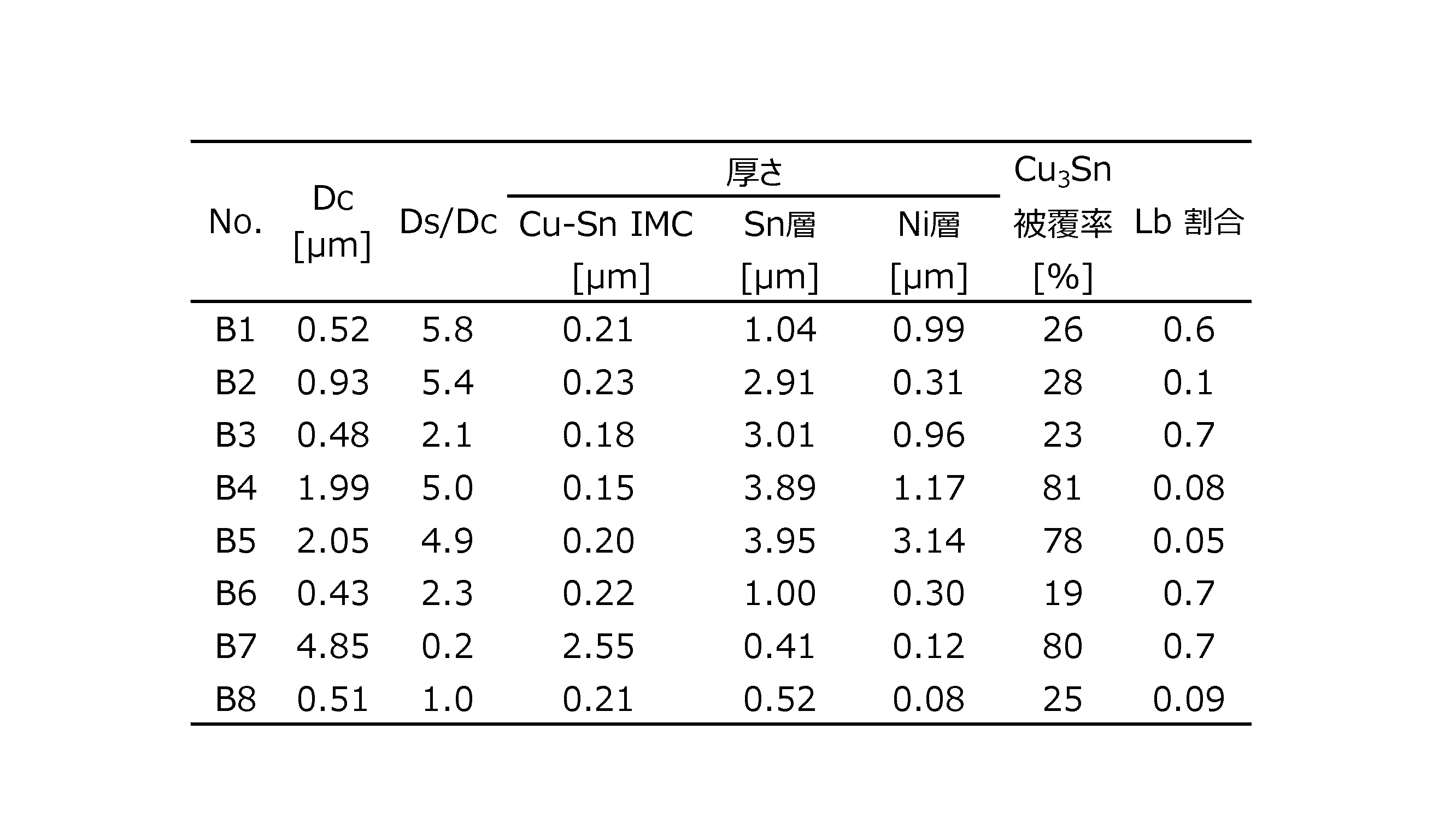
これらの試料につき、接触抵抗、残留Sn、曲げ加工性について評価した。接触抵抗および残留Snについては、以下に示す高温保持試験後の評価結果である。曲げ加工性は、高温保持試験前の評価結果である。
For these samples, contact resistance, residual Sn, and bending workability were evaluated. The contact resistance and residual Sn are the evaluation results after the high temperature holding test shown below. Bending workability is an evaluation result before the high temperature holding test.
(接触抵抗)
大気中で高温保持し(高温保持試験)、接触抵抗を測定した。保持条件は、Sn層の厚さが1.2μm以下の試料では125℃で1000時間とし、1.2μmより厚い試料では145℃で1000時間とした。測定方法はJIS-C-5402に準拠し、4端子接触抵抗試験機(山崎精機研究所製:CRS-113-AU)により、摺動式(1mm)で0から50gまでの荷重変化-接触抵抗を測定し、荷重を50gとしたときの接触抵抗値で評価した。 (Contact resistance)
It was held at a high temperature in the atmosphere (high temperature holding test), and the contact resistance was measured. The holding conditions were 125 ° C. for 1000 hours for a sample having a Sn layer thickness of 1.2 μm or less, and 145 ° C. for 1000 hours for a sample thicker than 1.2 μm. The measurement method conforms to JIS-C-5402, and a 4-terminal contact resistance tester (manufactured by Yamasaki Seiki Laboratory: CRS-113-AU) is a sliding type (1 mm) load change from 0 to 50 g-contact resistance. Was measured and evaluated by the contact resistance value when the load was 50 g.
1000時間経過後においても接触抵抗が2mΩ以下であったものをA、1000時間経過後には2mΩを上回るが500時間経過時点では2mΩ以下であったものをB、500時間経過時点で2mΩを上回ったものをCと評価した。
The one whose contact resistance was 2 mΩ or less even after 1000 hours passed was A, the one whose contact resistance exceeded 2 mΩ after 1000 hours but was 2 mΩ or less after 500 hours, and B, which exceeded 2 mΩ after 500 hours. The thing was evaluated as C.
(残留Sn)
リフロー直後の合金化していないSnの膜厚に対する、高温保持試験実施後に合金化せず残ったSnの膜厚の割合を残留Snとして評価した。すなわち、リフロー直後に合金化していないSnが高温保持試験後にどの程度残ったかを示している。高温保持試験条件は接触抵抗の場合と同様とした。1000時間経過後に50%を超えるものをA、25%を超えて50%以下のものをB、25%以下であったものをCと評価した。 (Residual Sn)
The ratio of the film thickness of the unalloyed Sn to the film thickness of the unalloyed Sn immediately after the reflow was evaluated as the residual Sn. That is, it shows how much unalloyed Sn remained after the high temperature holding test immediately after the reflow. The high temperature holding test conditions were the same as for the contact resistance. After 1000 hours, those exceeding 50% were evaluated as A, those exceeding 25% and 50% or less were evaluated as B, and those exceeding 25% were evaluated as C.
(曲げ加工性)
曲げ加工性は、試料(圧延材)を圧延垂直方向に幅10mm×長さ60mm(圧延方向60mm、幅方向10mm)に切出し、JIS Z 2248に規定される金属材料曲げ試験方法に準拠し、押し金具の曲げ半径Rと試料の厚さtとの比R/t=1として180°曲げ試験(曲げ方向:Bad Way)を行い、曲げ部の表面及び断面にクラック等が認められるか否かを光学顕微鏡にて倍率50倍で観察した。クラック等が認められず、表面状態も曲げの前後でクラック等、大きな変化が認められなかったものを「OK」、クラックが認められたものを「NG」とした。 (Bending workability)
For bending workability, a sample (rolled material) is cut out in the vertical direction of rolling to a width of 10 mm x a length of 60 mm (rolling direction 60 mm, width direction 10 mm), and pressed in accordance with the metal material bending test method specified in JIS Z 2248. A 180 ° bending test (bending direction: Bad Way) was performed with the ratio R / t = 1 of the bending radius R of the metal fitting to the thickness t of the sample, and whether or not cracks were found on the surface and cross section of the bent portion was determined. It was observed with an optical microscope at a magnification of 50 times. No cracks or the like were observed, and the surface condition was “OK” when no major changes such as cracks were observed before and after bending, and “NG” when cracks were observed.
これらの結果を表9~13に示す。
These results are shown in Tables 9-13.

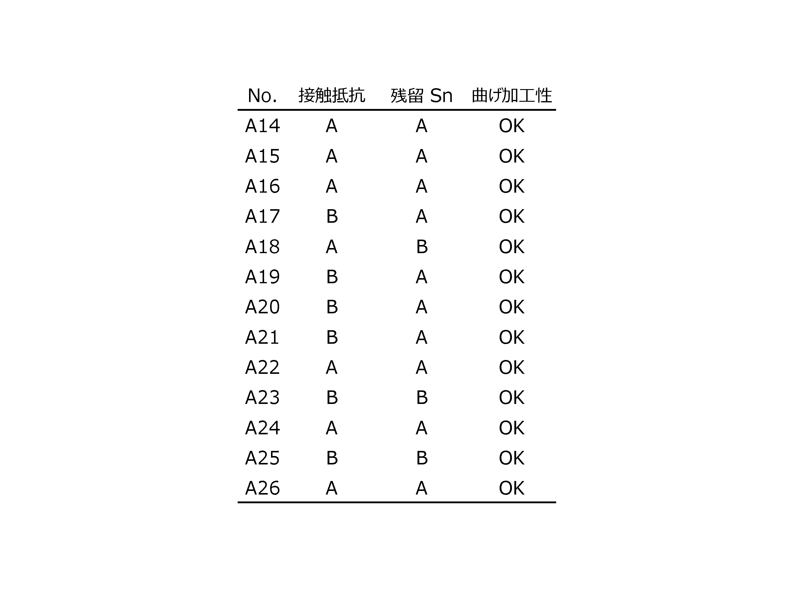


これらの結果より、Ni層の厚さが0.1μm以上1.0μm以下であり、Cu-Sn金属間化合物層の厚さが0.2μm以上2.5μm以下であり、Sn層の厚さが0.5μm以上3.0μm以下であり、Cu-Sn金属間化合物層の平均結晶粒径Dcが0.5μm以上であり、Dcに対するSn層の平均結晶粒径Dsの粒径比Ds/Dcが5以下の実施例(試料A1~A52)は、いずれも耐熱性(接触抵抗、残留Sn)がBランク以上となることが確認された。また、いずれの実施例においても曲げ割れは認められず、良好な加工性を有していることも確認された。
From these results, the thickness of the Ni layer is 0.1 μm or more and 1.0 μm or less, the thickness of the Cu-Sn intermetallic compound layer is 0.2 μm or more and 2.5 μm or less, and the thickness of the Sn layer is The average crystal grain size Dc of the Cu-Sn intermetallic compound layer is 0.5 μm or more and 3.0 μm or less, and the particle size ratio Ds / Dc of the average crystal grain size Ds of the Sn layer to Dc is It was confirmed that the heat resistance (contact resistance, residual Sn) of each of the examples 5 or less (Samples A1 to A52) was B rank or higher. In addition, no bending cracks were observed in any of the examples, and it was confirmed that the product had good workability.
これに対し比較例(試料B1~B8)は、粒径比Ds/DcやCu-Sn金属間化合物層の厚さ、Ni層の厚さ等のいずれかが本発明の範囲から外れており、その結果、耐熱性がCランクとなるか、あるいは曲げ加工性がNGであった。
On the other hand, in the comparative examples (Samples B1 to B8), any of the particle size ratio Ds / Dc, the thickness of the Cu—Sn intermetallic compound layer, the thickness of the Ni layer, etc. is out of the scope of the present invention. As a result, the heat resistance was C rank, or the bending workability was NG.
図3は、145℃×240時間保持した試料A27の皮膜断面のSEM像を示す。図4は、145℃×240時間保持した後、Sn層とCu-Sn金属間化合物層を剥離して観察した試料A27のNi層の表面SEM像を示す。
FIG. 3 shows an SEM image of a film cross section of sample A27 held at 145 ° C. for 240 hours. FIG. 4 shows a surface SEM image of the Ni layer of sample A27, which was observed by peeling off the Sn layer and the Cu—Sn intermetallic compound layer after holding at 145 ° C. for 240 hours.
断面SEM像において、高温保持後のCu-Sn金属間化合物層はCu6Sn5からなり、Cu-Sn金属間化合物層の薄い部位の直下にてNi層の損傷が確認された。Ni層の表面SEM像から、Ni層の損傷は網目状であることが確認された。このように本発明の実施例(試料A27)においても、長時間高温保持すると、Ni層の損傷が進行してNi層の一部が消失し、母材からのCuの外方拡散が進行するため耐熱性が劣化していくが、比較例に比べ劣化の速度は遅い。
In the cross-sectional SEM image, the Cu-Sn intermetallic compound layer after holding at a high temperature was composed of Cu 6 Sn 5 , and damage to the Ni layer was confirmed directly under the thin portion of the Cu-Sn intermetallic compound layer. From the surface SEM image of the Ni layer, it was confirmed that the damage of the Ni layer was reticulated. As described above, even in the embodiment of the present invention (Sample A27), when the high temperature is maintained for a long time, the damage of the Ni layer progresses, a part of the Ni layer disappears, and the outward diffusion of Cu from the base material proceeds. Therefore, the heat resistance deteriorates, but the rate of deterioration is slower than that of the comparative example.
145℃×240時間保持した試料B2(図5)と試料A48(図6)のNi層表面SEM像を示す。この図4~6のNi層表面SEM像を比較すると、A27よりもCu3Sn層被覆率の低いB2の方が、Ni層の損傷は大きい。一方、A27よりもCu3Sn層被覆率の高いA48では、Ni層の損傷がA27よりも少ない。このように、Cu3Sn被覆率の高い試料ではNi層の損傷が抑えられていることが明らかである。Ni層の損傷が生じ易い場所は、Cu-Sn金属間化合物層の薄い部位、すなわちCu6Sn5の島状結晶の端部近傍である。Cu3Sn層の被覆率が高くなると、Cu6Sn5層の島状結晶がより平坦に近くなり、極端に薄い部位が減少するためNi層の損傷が抑制され、耐熱性の向上が期待できる。
The Ni layer surface SEM image of the sample B2 (FIG. 5) and the sample A48 (FIG. 6) held at 145 ° C. for 240 hours is shown. Comparing the SEM images of the Ni layer surface shown in FIGS. 4 to 6, the damage of the Ni layer is larger in B2 having a lower Cu 3 Sn layer coverage than in A27. On the other hand, in A48, which has a higher Cu 3 Sn layer coverage than A27, the damage of the Ni layer is less than that of A27. As described above, it is clear that the damage of the Ni layer is suppressed in the sample having a high Cu 3 Sn coverage. The place where the Ni layer is easily damaged is a thin portion of the Cu-Sn intermetallic compound layer, that is, near the end of the island-shaped crystal of Cu 6 Sn 5. When the coverage of the Cu 3 Sn layer becomes high, the island-shaped crystals of the Cu 6 Sn 5 layer become closer to flat, and extremely thin parts are reduced, so that damage to the Ni layer is suppressed and heat resistance can be expected to be improved. ..
Ni層、Cu-Sn金属間化合物層、Sn層が順次形成されてなる端子材における耐熱性を向上させる。
Improves heat resistance in terminal materials in which a Ni layer, a Cu-Sn intermetallic compound layer, and a Sn layer are sequentially formed.
1 コネクタ用端子材
2 基材
3 Ni層
4 Cu-Sn金属間化合物層
41 Cu3Sn層
42 Cu6Sn5層
5 Sn層 1 Terminal material forconnector 2 Base material 3 Ni layer 4 Cu-Sn intermetallic compound layer 41 Cu 3 Sn layer 42 Cu 6 Sn 5 layer 5 Sn layer
2 基材
3 Ni層
4 Cu-Sn金属間化合物層
41 Cu3Sn層
42 Cu6Sn5層
5 Sn層 1 Terminal material for
Claims (5)
- 少なくとも表面がCu又はCu合金からなる基材と、
前記基材の上に形成され、Ni又はNi合金からなるNi層と、
前記Ni層の上に形成され、Cu6Sn5を有するCu-Sn金属間化合物層と、
前記Cu-Sn金属間化合物層の上に形成され、Sn又はSn合金からなるSn層と、を有するコネクタ用端子材であって、
前記Ni層の厚さが0.1μm以上1.0μm以下であり、前記Cu-Sn金属間化合物層の厚さが0.2μm以上2.5μm以下であり、前記Sn層の厚さが0.5μm以上3.0μm以下であり、
前記Cu-Sn金属間化合物層及び前記Sn層の断面をEBSD法により0.1μmの測定ステップで解析して、隣接するピクセル間の方位差が2°以上である境界を結晶粒界とみなし、前記Cu-Sn金属間化合物層における前記Cu6Sn5の平均結晶粒径をDcとし、前記Sn層の平均結晶粒径をDsとすると、平均結晶粒径Dcが0.5μm以上であり、粒径比Ds/Dcが5以下であることを特徴とするコネクタ用端子材。 At least a base material whose surface is made of Cu or Cu alloy,
A Ni layer formed on the base material and made of Ni or a Ni alloy,
A Cu-Sn intermetallic compound layer formed on the Ni layer and having Cu 6 Sn 5 and
A terminal material for a connector formed on the Cu-Sn intermetallic compound layer and having a Sn layer made of Sn or a Sn alloy.
The thickness of the Ni layer is 0.1 μm or more and 1.0 μm or less, the thickness of the Cu-Sn intermetallic compound layer is 0.2 μm or more and 2.5 μm or less, and the thickness of the Sn layer is 0. 5 μm or more and 3.0 μm or less,
The cross sections of the Cu-Sn intermetallic compound layer and the Sn layer are analyzed by the EBSD method in a measurement step of 0.1 μm, and the boundary where the orientation difference between adjacent pixels is 2 ° or more is regarded as a grain boundary. Assuming that the average crystal grain size of Cu 6 Sn 5 in the Cu-Sn intermetallic compound layer is Dc and the average crystal grain size of the Sn layer is Ds, the average crystal grain size Dc is 0.5 μm or more, and the grains are grains. A terminal material for a connector characterized in that the diameter ratio Ds / Dc is 5 or less. - 前記Cu-Sn金属間化合物層は、前記Ni層の上に形成されたCu3Sn層と、前記Cu3Sn層の上に形成された前記Cu6Sn5層とからなり、前記Ni層に対する前記Cu3Sn層の被覆率は20%以上であることを特徴とする請求項1に記載のコネクタ用端子材。 The Cu-Sn metal-to-metal compound layer is composed of a Cu 3 Sn layer formed on the Ni layer and the Cu 6 Sn 5 layer formed on the Cu 3 Sn layer with respect to the Ni layer. The terminal material for a connector according to claim 1, wherein the coverage of the Cu 3 Sn layer is 20% or more.
- 前記Sn層は凝固組織からなることを特徴とする請求項1又は2に記載のコネクタ用端子材。 The terminal material for a connector according to claim 1 or 2, wherein the Sn layer is composed of a solidified structure.
- 前記Sn層は、前記EBSD法により画定した結晶粒界のうち、前記方位差が15°以上の結晶の粒界長さをLaとし、前記方位差が2°以上15°未満の結晶の粒界長さをLbとすると、Lb割合(Lb/(Lb+La))が0.1以上であることを特徴とする請求項1から3のいずれか一項に記載のコネクタ用端子材。 Among the grain boundaries defined by the EBSD method, the Sn layer has a grain boundary length of a crystal having an orientation difference of 15 ° or more as La, and a grain boundary of a crystal having an orientation difference of 2 ° or more and less than 15 °. The terminal material for a connector according to any one of claims 1 to 3, wherein the Lb ratio (Lb / (Lb + La)) is 0.1 or more, where Lb is the length.
- 少なくとも表面がCu又はCu合金からなる基材の表面に、Ni又はNi合金からなるめっき層を形成するNiめっき処理、Cu又はCu合金からなるめっき層を形成するCuめっき処理、Sn又はSn合金からなるめっき層を形成するSnめっき処理をこの順に施すめっき処理工程と、
前記めっき処理工程の後、リフロー処理するリフロー処理工程と、を有し、
前記基材の上にNi又はNi合金からなるNi層が形成され、前記Ni層の上にCu及びSnの金属間化合物からなるCu-Sn金属間化合物層が形成され、前記Cu-Sn金属間化合物層の上にSn又はSn合金からなるSn層が形成されてなるコネクタ用端子材を製造する方法であって、
前記リフロー処理は、20℃/秒以上75℃/秒以下の昇温速度で240℃以上に加熱する一次加熱処理と、前記一次加熱処理の後に、240℃以上300℃以下の温度で1秒以上15秒以下の時間加熱する二次加熱処理とを行う加熱工程と、
前記加熱工程の後に、30℃/秒以下の冷却速度で冷却する一次冷却工程と、
前記一次冷却後に100℃/秒以上300℃/秒以下の冷却速度で冷却する二次冷却工程と
を有することを特徴とするコネクタ用端子材の製造方法。 Ni plating treatment to form a plating layer made of Ni or Ni alloy on the surface of a base material whose surface is at least Cu or Cu alloy, Cu plating treatment to form a plating layer made of Cu or Cu alloy, Sn or Sn alloy A plating process in which Sn plating is performed in this order to form a plating layer, and
After the plating treatment step, it has a reflow treatment step of reflowing.
A Ni layer made of Ni or a Ni alloy is formed on the base material, a Cu-Sn intermetallic compound layer made of an intermetallic compound of Cu and Sn is formed on the Ni layer, and the Cu-Sn intermetallic layer is formed. A method for producing a terminal material for a connector in which a Sn layer made of Sn or a Sn alloy is formed on a compound layer.
The reflow treatment includes a primary heat treatment of heating to 240 ° C. or higher at a heating rate of 20 ° C./sec or higher and 75 ° C./sec or lower, and a temperature of 240 ° C. or higher and 300 ° C. or lower for 1 second or longer after the primary heat treatment. A heating step of performing a secondary heat treatment of heating for a time of 15 seconds or less, and
After the heating step, a primary cooling step of cooling at a cooling rate of 30 ° C./sec or less and a primary cooling step.
A method for manufacturing a terminal material for a connector, which comprises a secondary cooling step of cooling at a cooling rate of 100 ° C./sec or more and 300 ° C./sec or less after the primary cooling.
Priority Applications (4)
| Application Number | Priority Date | Filing Date | Title |
|---|---|---|---|
| US17/764,261 US11905614B2 (en) | 2019-09-30 | 2020-09-29 | Terminal material for connector |
| KR1020227009677A KR20220069005A (en) | 2019-09-30 | 2020-09-29 | Terminal material for connector |
| CN202080068848.1A CN114466942A (en) | 2019-09-30 | 2020-09-29 | Terminal material for connector |
| EP20872327.0A EP4039855A4 (en) | 2019-09-30 | 2020-09-29 | Terminal material for connectors |
Applications Claiming Priority (2)
| Application Number | Priority Date | Filing Date | Title |
|---|---|---|---|
| JP2019-181011 | 2019-09-30 | ||
| JP2019181011A JP7272224B2 (en) | 2019-09-30 | 2019-09-30 | Terminal materials for connectors |
Publications (1)
| Publication Number | Publication Date |
|---|---|
| WO2021065866A1 true WO2021065866A1 (en) | 2021-04-08 |
Family
ID=75272272
Family Applications (1)
| Application Number | Title | Priority Date | Filing Date |
|---|---|---|---|
| PCT/JP2020/036807 WO2021065866A1 (en) | 2019-09-30 | 2020-09-29 | Terminal material for connectors |
Country Status (7)
| Country | Link |
|---|---|
| US (1) | US11905614B2 (en) |
| EP (1) | EP4039855A4 (en) |
| JP (1) | JP7272224B2 (en) |
| KR (1) | KR20220069005A (en) |
| CN (1) | CN114466942A (en) |
| TW (1) | TW202129019A (en) |
| WO (1) | WO2021065866A1 (en) |
Families Citing this family (2)
| Publication number | Priority date | Publication date | Assignee | Title |
|---|---|---|---|---|
| JP6957568B2 (en) * | 2019-08-09 | 2021-11-02 | 株式会社オートネットワーク技術研究所 | Wire with terminal |
| JP6936836B2 (en) | 2019-08-09 | 2021-09-22 | 株式会社オートネットワーク技術研究所 | Wire with terminal |
Citations (7)
| Publication number | Priority date | Publication date | Assignee | Title |
|---|---|---|---|---|
| JP2003293187A (en) | 2002-03-29 | 2003-10-15 | Dowa Mining Co Ltd | Copper or copper alloy subjected to plating and method for manufacturing the same |
| JP2010168598A (en) * | 2009-01-20 | 2010-08-05 | Mitsubishi Shindoh Co Ltd | Conductive member and method for manufacturing the same |
| JP2010280946A (en) | 2009-06-04 | 2010-12-16 | Mitsubishi Shindoh Co Ltd | Plated copper wire and method for manufacturing the same |
| JP2014122403A (en) | 2012-12-21 | 2014-07-03 | Mitsubishi Materials Corp | Tin-plated electroconductive material and production method thereof |
| JP2016056424A (en) * | 2014-09-11 | 2016-04-21 | 三菱マテリアル株式会社 | Tin-plated copper alloy terminal material and a method for manufacturing the same |
| WO2018135482A1 (en) * | 2017-01-17 | 2018-07-26 | 三菱伸銅株式会社 | Terminal material for connectors and method for producing same |
| JP2019181011A (en) | 2018-04-16 | 2019-10-24 | 株式会社高尾 | Reel type game machine |
Family Cites Families (5)
| Publication number | Priority date | Publication date | Assignee | Title |
|---|---|---|---|---|
| KR101596342B1 (en) | 2009-01-20 | 2016-02-22 | 미츠비시 신도 가부시키가이샤 | Conductive member and method for producing the same |
| CN102395713B (en) * | 2009-04-14 | 2014-07-16 | 三菱伸铜株式会社 | Conductive member and manufacturing method thereof |
| JP5280957B2 (en) * | 2009-07-28 | 2013-09-04 | 三菱伸銅株式会社 | Conductive member and manufacturing method thereof |
| JP6000392B1 (en) * | 2015-03-23 | 2016-09-28 | 株式会社神戸製鋼所 | Conductive material for connecting parts |
| KR101900793B1 (en) * | 2017-06-08 | 2018-09-20 | 주식회사 풍산 | A method for tin plating copper alloy for electrical and electronic and car components, and tin plated copper alloy therefrom |
-
2019
- 2019-09-30 JP JP2019181011A patent/JP7272224B2/en active Active
-
2020
- 2020-09-29 EP EP20872327.0A patent/EP4039855A4/en active Pending
- 2020-09-29 US US17/764,261 patent/US11905614B2/en active Active
- 2020-09-29 KR KR1020227009677A patent/KR20220069005A/en unknown
- 2020-09-29 WO PCT/JP2020/036807 patent/WO2021065866A1/en unknown
- 2020-09-29 CN CN202080068848.1A patent/CN114466942A/en active Pending
- 2020-09-30 TW TW109134078A patent/TW202129019A/en unknown
Patent Citations (7)
| Publication number | Priority date | Publication date | Assignee | Title |
|---|---|---|---|---|
| JP2003293187A (en) | 2002-03-29 | 2003-10-15 | Dowa Mining Co Ltd | Copper or copper alloy subjected to plating and method for manufacturing the same |
| JP2010168598A (en) * | 2009-01-20 | 2010-08-05 | Mitsubishi Shindoh Co Ltd | Conductive member and method for manufacturing the same |
| JP2010280946A (en) | 2009-06-04 | 2010-12-16 | Mitsubishi Shindoh Co Ltd | Plated copper wire and method for manufacturing the same |
| JP2014122403A (en) | 2012-12-21 | 2014-07-03 | Mitsubishi Materials Corp | Tin-plated electroconductive material and production method thereof |
| JP2016056424A (en) * | 2014-09-11 | 2016-04-21 | 三菱マテリアル株式会社 | Tin-plated copper alloy terminal material and a method for manufacturing the same |
| WO2018135482A1 (en) * | 2017-01-17 | 2018-07-26 | 三菱伸銅株式会社 | Terminal material for connectors and method for producing same |
| JP2019181011A (en) | 2018-04-16 | 2019-10-24 | 株式会社高尾 | Reel type game machine |
Non-Patent Citations (1)
| Title |
|---|
| See also references of EP4039855A4 |
Also Published As
| Publication number | Publication date |
|---|---|
| CN114466942A (en) | 2022-05-10 |
| US20220380924A1 (en) | 2022-12-01 |
| US11905614B2 (en) | 2024-02-20 |
| JP7272224B2 (en) | 2023-05-12 |
| KR20220069005A (en) | 2022-05-26 |
| EP4039855A4 (en) | 2023-12-06 |
| TW202129019A (en) | 2021-08-01 |
| EP4039855A1 (en) | 2022-08-10 |
| JP2021055163A (en) | 2021-04-08 |
Similar Documents
| Publication | Publication Date | Title |
|---|---|---|
| TWI570283B (en) | Metallic copper alloy terminal material with excellent plugability and manufacturing method thereof | |
| US20180301838A1 (en) | Copper alloy sheet with sn coating layer for a fitting type connection terminal and a fitting type connection terminal | |
| US20190249274A1 (en) | Conductive material for connection parts which has excellent minute slide wear resistance | |
| EP2703524A2 (en) | Sn-coated copper alloy strip having excellent heat resistance | |
| JP6160582B2 (en) | Tin-plated copper alloy terminal material and manufacturing method thereof | |
| WO2015125927A1 (en) | Surface coating layer-equipped copper alloy plate strip having excellent heat resistance | |
| JP2010265542A (en) | Conductive member and manufacturing method thereof | |
| TW201413068A (en) | Tin-plated copper alloy terminal member with outstanding insertion and removal characteristics and method of manufacturing the same | |
| WO2021065866A1 (en) | Terminal material for connectors | |
| JP2010168598A (en) | Conductive member and method for manufacturing the same | |
| CN110997985A (en) | Silver-coated membrane terminal material and silver-coated membrane terminal | |
| JP2010196084A (en) | Electroconductive member and production method therefor | |
| US10998108B2 (en) | Electrical contact material, method of producing an electrical contact material, and terminal | |
| KR20150050397A (en) | Tin-plated copper alloy terminal member | |
| JP5325734B2 (en) | Conductive member and manufacturing method thereof | |
| JP2005226097A (en) | Tinned copper alloy material for electrical/electronic component, and its production method | |
| TW202100810A (en) | Anti-corrosion terminal material, terminal, and electrical wire end section structure | |
| JP6219553B2 (en) | Plating material excellent in heat resistance and method for producing the same | |
| JP2005154819A (en) | Fitting type connection terminal | |
| JP7281971B2 (en) | Electrical contact material and its manufacturing method, connector terminal, connector and electronic component | |
| JP7281970B2 (en) | Electrical contact material and its manufacturing method, connector terminal, connector and electronic component | |
| JP7087732B2 (en) | Conductive member for connector terminal and connector terminal | |
| JP5367271B2 (en) | Rolled plate | |
| JP2020056090A (en) | Anticorrosive terminal material, manufacturing method therefor, and anticorrosive terminal and wire terminal part structure | |
| JP7353928B2 (en) | Materials for electrical contacts and their manufacturing methods, connector terminals, connectors, and electronic components |
Legal Events
| Date | Code | Title | Description |
|---|---|---|---|
| 121 | Ep: the epo has been informed by wipo that ep was designated in this application |
Ref document number: 20872327 Country of ref document: EP Kind code of ref document: A1 |
|
| NENP | Non-entry into the national phase |
Ref country code: DE |
|
| ENP | Entry into the national phase |
Ref document number: 2020872327 Country of ref document: EP Effective date: 20220502 |