WO2021038868A1 - 直流電源装置、モータ駆動装置、送風機、圧縮機及び空気調和機 - Google Patents
直流電源装置、モータ駆動装置、送風機、圧縮機及び空気調和機 Download PDFInfo
- Publication number
- WO2021038868A1 WO2021038868A1 PCT/JP2019/034262 JP2019034262W WO2021038868A1 WO 2021038868 A1 WO2021038868 A1 WO 2021038868A1 JP 2019034262 W JP2019034262 W JP 2019034262W WO 2021038868 A1 WO2021038868 A1 WO 2021038868A1
- Authority
- WO
- WIPO (PCT)
- Prior art keywords
- power supply
- voltage
- switching element
- switching
- converter
- Prior art date
- Legal status (The legal status is an assumption and is not a legal conclusion. Google has not performed a legal analysis and makes no representation as to the accuracy of the status listed.)
- Ceased
Links
Images




Classifications
-
- H—ELECTRICITY
- H02—GENERATION; CONVERSION OR DISTRIBUTION OF ELECTRIC POWER
- H02M—APPARATUS FOR CONVERSION BETWEEN AC AND AC, BETWEEN AC AND DC, OR BETWEEN DC AND DC, AND FOR USE WITH MAINS OR SIMILAR POWER SUPPLY SYSTEMS; CONVERSION OF DC OR AC INPUT POWER INTO SURGE OUTPUT POWER; CONTROL OR REGULATION THEREOF
- H02M7/00—Conversion of AC power input into DC power output; Conversion of DC power input into AC power output
- H02M7/02—Conversion of AC power input into DC power output without possibility of reversal
- H02M7/04—Conversion of AC power input into DC power output without possibility of reversal by static converters
- H02M7/12—Conversion of AC power input into DC power output without possibility of reversal by static converters using discharge tubes with control electrode or semiconductor devices with control electrode
-
- H—ELECTRICITY
- H02—GENERATION; CONVERSION OR DISTRIBUTION OF ELECTRIC POWER
- H02M—APPARATUS FOR CONVERSION BETWEEN AC AND AC, BETWEEN AC AND DC, OR BETWEEN DC AND DC, AND FOR USE WITH MAINS OR SIMILAR POWER SUPPLY SYSTEMS; CONVERSION OF DC OR AC INPUT POWER INTO SURGE OUTPUT POWER; CONTROL OR REGULATION THEREOF
- H02M7/00—Conversion of AC power input into DC power output; Conversion of DC power input into AC power output
- H02M7/02—Conversion of AC power input into DC power output without possibility of reversal
- H02M7/04—Conversion of AC power input into DC power output without possibility of reversal by static converters
- H02M7/12—Conversion of AC power input into DC power output without possibility of reversal by static converters using discharge tubes with control electrode or semiconductor devices with control electrode
- H02M7/21—Conversion of AC power input into DC power output without possibility of reversal by static converters using discharge tubes with control electrode or semiconductor devices with control electrode using devices of a triode or transistor type requiring continuous application of a control signal
-
- Y—GENERAL TAGGING OF NEW TECHNOLOGICAL DEVELOPMENTS; GENERAL TAGGING OF CROSS-SECTIONAL TECHNOLOGIES SPANNING OVER SEVERAL SECTIONS OF THE IPC; TECHNICAL SUBJECTS COVERED BY FORMER USPC CROSS-REFERENCE ART COLLECTIONS [XRACs] AND DIGESTS
- Y02—TECHNOLOGIES OR APPLICATIONS FOR MITIGATION OR ADAPTATION AGAINST CLIMATE CHANGE
- Y02B—CLIMATE CHANGE MITIGATION TECHNOLOGIES RELATED TO BUILDINGS, e.g. HOUSING, HOUSE APPLIANCES OR RELATED END-USER APPLICATIONS
- Y02B70/00—Technologies for an efficient end-user side electric power management and consumption
- Y02B70/10—Technologies improving the efficiency by using switched-mode power supplies [SMPS], i.e. efficient power electronics conversion e.g. power factor correction or reduction of losses in power supplies or efficient standby modes
Definitions
- the present invention includes a DC power supply device that converts an AC voltage output from an AC power supply into a DC voltage and applies it to a load, a motor drive device that drives a motor that is a load, a blower and a compressor equipped with a motor drive device, and , With respect to an air conditioner equipped with a blower or compressor.
- Patent Document 1 describes a connection point between a first diode and a second diode, and a connection between a first metal oxide semiconductor field effect transistor (Metal Oxide Semiconductor Field Effect Transistor: MOSFET) and a second MOSFET.
- a DC power supply device is disclosed in which an AC power supply is connected via a reactor and the AC voltage of the AC power supply is converted into a DC voltage by switching between the first MOSFET and the second MOSFET.
- the first diode and the first MOSFET are elements connected to the positive electrode side of the smoothing capacitor, and the second diode and the second MOSFET are elements connected to the negative electrode side of the smoothing capacitor.
- the first MOSFET is turned on at the timing when the current flows through the parasitic diode of the first MOSFET, and the second MOSFET is operated at the timing when the current flows through the parasitic diode of the second MOSFET.
- This technique is called synchronous rectification.
- the DC power supply is controlled with high efficiency by synchronous rectification.
- each MOSFET is always turned on at the timing when the current flows through the parasitic diodes of the first and second MOSFETs.
- the efficiency of the synchronous rectification operation is improved on the premise that the voltage drop of the parasitic diodes connected in parallel is higher than the on-voltage of the MOSFET.
- the on-voltage of the MOSFET may be higher than the voltage drop of the parasitic diodes connected in parallel. Therefore, it cannot be said that the synchronous rectification described in Patent Document 1 is optimized for the operation of the synchronous rectification. Therefore, the technique of Patent Document 1 has room for improvement in terms of efficiency when applying synchronous rectification.
- the present invention has been made in view of the above, and an object of the present invention is to obtain a DC power supply device capable of further improving efficiency when applying synchronous rectification.
- the DC power supply device includes a reactor and four unidirectional elements connected by a bridge, and is connected to an AC power supply via the reactor to be connected to an AC power supply. It includes a converter that converts the power supply voltage, which is an AC voltage output from the AC voltage, into a DC voltage and applies it to the load, and a smoothing capacitor connected between the output terminals of the converter. Further, the DC power supply device has a first physical quantity detection unit that detects a first physical quantity that represents the operating state of the output side of the converter, and a second physical quantity that detects a second physical quantity that represents the operating state of the input side of the converter.
- the control unit includes a physical quantity detecting unit and a control unit in which first and second physical quantities are input and controls the operation of the converter.
- Two of the four unidirectional elements in the converter are connected in series to form the first leg, and the remaining two unidirectional elements are connected in series to form the second leg.
- At least two unidirectional elements in the first and second legs connected to the positive side of the smoothing capacitor, or two in the first and second legs connected to the negative side of the smoothing capacitor.
- a switching element is connected in parallel to each of the unidirectional element, the two unidirectional elements in the first leg, or the two unidirectional elements in the second leg.
- the control unit further has a plurality of operation modes for operating the converter in different operation modes by controlling the conduction of the switching element according to the ambient temperature of the switching element, the outside air temperature of the converter, or the operation command to the converter.
- FIG. 3 shows a path of a current flowing through the converter according to the first embodiment.
- FIG. 4 shows a path of a current flowing through a converter according to the first embodiment.
- Flow chart used to explain the operation of the main part in the first embodiment The figure which shows the temperature characteristic of the forward current of a parasitic diode in a general MOSFET.
- the figure which shows the temperature characteristic of the on-resistance of a general MOSFET The figure which shows how the cross point shown in FIG. 9 fluctuates with temperature.
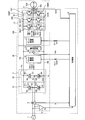
- FIG. 1 is a diagram showing a configuration example of a motor drive device 100 including a DC power supply device 50 according to the first embodiment.
- the DC power supply device 50 according to the first embodiment is a power supply device that converts a power supply voltage, which is an AC voltage output from a single-phase AC power supply 1, into a DC voltage and applies it to a load 12.
- the motor drive device 100 according to the first embodiment is a drive device that converts the DC power output from the DC power supply device 50 into AC power and supplies the converted AC power to the motor 500 to drive the motor 500. is there.
- the motor drive device 100 includes a DC power supply device 50, a control unit 10, and a load 12 as main components.
- the DC power supply device 50 includes a reactor 2, a converter 3, a gate drive circuit 15 which is a first drive circuit, a smoothing capacitor 4, a voltage detection unit 5, a current detection unit 6, and a voltage detection unit 7. It includes a power supply circuit 14 which is a control power supply.
- One end of the reactor 2 is connected to the AC power supply 1, and the other end of the reactor 2 is connected to the converter 3.
- the reactor 2 temporarily stores the electric power supplied from the AC power source 1.
- the converter 3 converts the AC voltage output from the AC power supply 1 into a DC voltage and outputs the AC voltage to the DC bus 16a and 16b.
- the DC bus lines 16a and 16b are electrical wirings that connect the converter 3 and the load 12. The voltage between the DC bus 16a and the DC bus 16b is called the "bus voltage".
- the load 12 includes a gate drive circuit 17, which is a second drive circuit, an inverter 18, a current detection unit 9, and a motor 500.
- the gate drive circuit 17, the inverter 18, and the current detection unit 9, excluding the motor 500 are the components of the motor drive device 100.
- the inverter 18 converts the DC voltage output from the DC power supply device 50 into an AC voltage applied to the motor 500 and outputs the AC voltage. Examples of equipment on which the motor 500 is mounted are blowers, compressors or air conditioners.
- FIG. 1 shows an example in which the device connected to the inverter 18 is the motor 500, but the present invention is not limited to this.
- the device connected to the inverter 18 may be any device to which AC power is input, and may be a device other than the motor 500.
- the converter 3 includes a first leg 31 and a second leg 32.
- the first leg 31 and the second leg 32 are connected in parallel.
- the first upper arm element 311 and the first lower arm element 312 are connected in series.
- the second upper arm element 321 and the second lower arm element 322 are connected in series.
- the other end of the reactor 2 is connected to a connection point 3a between the first upper arm element 311 and the first lower arm element 312 in the first leg 31.
- the connection point 3b between the second upper arm element 321 and the second lower arm element 322 is connected to the other end of the AC power supply 1.
- the connection points 3a and 3b form an AC terminal.
- the reactor 2 is connected between one end of the AC power supply 1 and the connection point 3a, but is connected between another end of the AC power supply 1 and the connection point 3b. May be good.
- the side where the connection points 3a and 3b are located is called the "AC side"
- the AC voltage output from the AC power supply 1 is called the “power supply voltage”
- the cycle of the power supply voltage is called the “power supply cycle”.
- the first upper arm element 311 includes a switching element Q1 and a diode D1 connected in parallel to the switching element Q1.
- the first lower arm element 312 includes a switching element Q2 and a diode D2 connected in parallel to the switching element Q2.
- the second upper arm element 321 includes a switching element Q3 and a diode D3 connected in parallel to the switching element Q3.
- the second lower arm element 322 includes a switching element Q4 and a diode D4 connected in parallel to the switching element Q4.
- the diodes D1 and D4 are unidirectional so that forward current flows when the polarity of the power supply voltage is positive, that is, the side connected to the reactor 2 has a higher potential than the side not connected to the reactor 2. It is an element.
- the diodes D2 and D3 are unidirectional so that a forward current flows when the polarity of the power supply voltage is negative, that is, the side not connected to the reactor 2 has a higher potential than the side connected to the reactor 2. It is an element.
- FIG. 1 discloses a configuration in which switching elements Q1, Q2, Q3, and Q4 are connected in parallel to each of the diodes D1, D2, D3, and D4, but the present invention is not limited to this.
- Switching elements may be connected to each of the two diodes connected to the positive side of the smoothing capacitor 4, that is, the diode D1 in the first leg 31 and the diode D3 in the second leg 32.
- switching elements may be connected to each of the two diodes connected to the negative side of the smoothing capacitor 4, that is, the diode D2 in the first leg 31 and the diode D4 in the second leg 32.
- a switching element may be connected to each of the two diodes in the first leg 31, that is, the diodes D1 and D2.
- a switching element may be connected to each of the two diodes in the second leg 32, that is, the diodes D3 and D4.
- MOSFETs are illustrated for each of the switching elements Q1, Q2, Q3, and Q4, but the limitation is not limited to MOSFETs.
- the MOSFET is a switching element capable of passing a current in both directions between the drain and the source. Any switching element may be used as long as it is a switching element capable of bidirectionally flowing a current between the first terminal corresponding to the drain and the second terminal corresponding to the source, that is, a bidirectional element.
- parallel here means that the first terminal corresponding to the drain of the MOSFET and the cathode of the diode are connected, and the second terminal corresponding to the source of the MOSFET and the anode of the diode are connected.
- a parasitic diode that the MOSFET itself has inside may be used. Parasitic diodes are also called body diodes.
- the switching elements Q1, Q2, Q3 and Q4 are not limited to MOSFETs formed of silicon-based materials, and are wide-band such as silicon carbide (SiC), gallium nitride (GaN), gallium oxide (Ga 2 O 3) or diamond. It may be a MOSFET formed of a bandgap (Wide Band Gap) semiconductor.
- WBG semiconductors have higher withstand voltage and heat resistance than silicon semiconductors. Therefore, by using a WBG semiconductor for at least one of the switching elements Q1, Q2, Q3, and Q4, the withstand voltage resistance and the allowable current density of the switching element are increased, and the semiconductor module incorporating the switching element is miniaturized. it can.
- a MOSFET having a Super Junction (SJ) structure may be used instead of the WBG semiconductor.
- SJ-MOSFET Super Junction
- the positive side of the smoothing capacitor 4 is connected to the DC bus 16a on the high potential side.
- the DC bus 16a is drawn from the connection point 3c between the first upper arm element 311 in the first leg 31 and the second upper arm element 321 in the second leg 32.
- the negative side of the smoothing capacitor 4 is connected to the DC bus 16b on the low potential side.
- the DC bus 16b is drawn from the connection point 3d between the first lower arm element 312 in the first leg 31 and the second lower arm element 322 in the second leg 32.
- the connection points 3c and 3d form a DC terminal.
- the side where the connection points 3c and 3d are located may be referred to as the "DC side".
- the output voltage of the converter 3 is applied to both ends of the smoothing capacitor 4.
- the smoothing capacitor 4 is connected to the DC bus lines 16a and 16b.
- the smoothing capacitor 4 smoothes the output voltage of the converter 3.
- the voltage smoothed by the smoothing capacitor 4 is applied to the inverter 18.
- the voltage detection unit 5 detects the power supply voltage and outputs the detected value Vs of the power supply voltage to the control unit 10.
- the power supply voltage is an absolute value of the instantaneous voltage of the AC power supply 1.
- the effective value of the instantaneous voltage may be used as the power supply voltage.
- the current detection unit 6 detects the power supply current, which is the AC current flowing between the AC power supply 1 and the converter 3, and outputs the detected value Is of the power supply current to the control unit 10.
- An example of a current detector used in the current detection unit 6 is an AC current transformer (Alternating Current Current Transformer: ACCT).
- the voltage detection unit 7 detects the bus voltage and outputs the detected value Vdc of the bus voltage to the control unit 10.
- the bus voltage is a physical quantity that represents the operating state of the DC side, that is, the output side of the converter 3.
- the power supply voltage is a physical quantity representing the operating state of the AC side, that is, the input side of the converter 3.
- the bus voltage may be referred to as a "first physical quantity” and the power supply voltage may be referred to as a "second physical quantity”.
- the voltage detection unit 7 that detects the bus voltage may be called a "first physical quantity detection unit”
- the voltage detection unit 5 that detects the power supply voltage may be called a "second physical quantity detection unit”.
- the power supply circuit 14 is connected to both ends of the smoothing capacitor 4.
- the power supply circuit 14 uses the voltage of the smoothing capacitor 4 to generate low-voltage DC voltages such as 5V, 12V, 15V, and 24V.
- the low-voltage DC voltage is generated by utilizing the electric charge accumulated in the smoothing capacitor 4.
- a low-voltage DC voltage is applied to each part of the supply destination as an operating voltage.
- the power supply circuit 14 outputs, for example, a DC voltage of 5 V to the control unit 10, the current detection unit 6, and the like. In the control unit 10, a DC voltage of 5 V is applied to a processor (not shown) in FIG.
- the inverter 18 includes a leg 18A in which the upper arm element 18UP and the lower arm element 18UN are connected in series, a leg 18B in which the upper arm element 18VP and the lower arm element 18VN are connected in series, and the upper arm element 18WP and the lower. It includes a leg 18C in which an arm element 18WN is connected in series.
- the legs 18A, 18B and 18C are connected in parallel to each other.
- FIG. 1 illustrates a case where the upper arm elements 18UP, 18VP, 18WP and the lower arm elements 18UN, 18VN, 18WN are insulated gate bipolar transistors (Insulated Gate Bipolar Transistors: IGBTs), but the present invention is not limited thereto. Instead of the IGBT, a MOSFET or an integrated gate commutated thyristor (IGCT) may be used.
- IGBTs Insulated Gate Bipolar Transistors
- IGCT integrated gate commutated thyristor
- the upper arm element 18UP includes a transistor 18a and a diode 18b connected in parallel to the transistor 18a.
- the other upper arm elements 18VP and 18WP and the lower arm elements 18UN, 18VN and 18WN have the same configuration.
- the term "parallel" as used herein means that the anode side of the diode is connected to the first terminal corresponding to the emitter of the IGBT, and the cathode side of the diode is connected to the second terminal corresponding to the collector of the IGBT.
- FIG. 1 has a configuration including three legs in which the upper arm element and the lower arm element are connected in series, but the configuration is not limited to this. The number of legs may be four or more.
- the circuit configuration shown in FIG. 1 is adapted to the motor 500, which is a three-phase motor.
- the motor 500 is a single-phase motor
- the inverter 18 is also configured to correspond to the single-phase motor.
- the configuration is provided with two legs in which the upper arm element and the lower arm element are connected in series.
- one leg may be composed of a plurality of pairs of upper and lower arm elements.
- the transistor 18a of the upper arm elements 18UP, 18VP, 18WP and the lower arm elements 18UN, 18VN, 18WN is a MOSFET
- the upper arm elements 18UP, 18VP, 18WP and the lower arm elements 18UN, 18VN, 18WN are silicon carbide, gallium nitride. It may be formed of a system material or a WBG semiconductor such as diamond. If a MOSFET formed of a WBG semiconductor is used, the effects of withstand voltage and heat resistance can be enjoyed.
- connection point 26a between the upper arm element 18UP and the lower arm element 18UN is connected to the first phase (for example, U phase) of the motor 500
- the connection point 26b between the upper arm element 18VP and the lower arm element 18VN is the first phase of the motor 500. It is connected to the second phase (for example, V phase)
- the connection point 26c between the upper arm element 18WP and the lower arm element 18WN is connected to the third phase (for example, W phase) of the motor 500.
- the connection points 26a, 26b, and 26c form an AC terminal.
- the current detection unit 9 detects the motor current flowing between the inverter 18 and the motor 500, and outputs the detected value Iuvw of the motor current to the control unit 10.
- the control unit 10 controls each switching element in the converter 3 based on the detection value Vs of the voltage detection unit 5, the detection value Is of the current detection unit 6, and the detection value Vdc of the voltage detection unit 7. Generate S311 to S322.
- the control signal S311 is a control signal for controlling the switching element Q1
- the control signal S322 is a control signal for controlling the switching element Q4.
- the switching elements Q2 and Q3 are also controlled by the control signal from the control unit 10.
- switching operation of each arm element according to the control signals S311 to S322 is appropriately referred to as “switching operation”.
- the control signals S311 to S322 generated by the control unit 10 are input to the gate drive circuit 15.
- control unit 10 is provided with each switching element in the inverter 18 so that the motor 500 rotates at a desired rotation speed based on the detection value Vdc of the voltage detection unit 7 and the detection value Iuvw of the current detection unit 9.
- Control signals S1 to S6 for controlling the above are generated.
- the inverter 18 has a three-phase circuit configuration, and has six switching elements corresponding to the three-phase circuit configuration. Further, six control signals S1 to S6 are generated corresponding to the six switching elements.
- the control signals S1 to S6 generated by the control unit 10 are input to the gate drive circuit 17.
- the gate drive circuit 15 generates drive pulses G311 to G322 for driving each switching element in the converter 3 based on the control signals S311 to S322.
- the drive pulse G311 is a drive pulse for driving the switching element Q1
- the drive pulse G322 is a drive pulse for driving the switching element Q4.
- the switching elements Q2 and Q3 are also driven by the drive pulse from the gate drive circuit 15.
- the gate drive circuit 17 generates drive pulses G1 to G6 for driving each switching element in the inverter 18 based on the control signals S1 to S6.
- control unit 10 is provided inside the motor drive device 100 as a common control unit for controlling the DC power supply device 50 and the load 12, but the configuration is not limited to this. Individual control units that control each of the DC power supply device 50 and the load 12 may be configured, and each control unit may be provided inside each of the DC power supply device 50 and the load 12.
- the first upper arm element 311 and the first lower arm element 312 operate so as to be complementary or not turned on at the same time. That is, when one of the first upper arm element 311 and the first lower arm element 312 is on, the other is off.
- the first upper arm element 311 and the first lower arm element 312 are controlled by the control signals S311 and S312 generated by the control unit 10.
- An example of the control signals S311 and S312 is a pulse width modulation (PWM) signal.
- PWM pulse width modulation
- Capacitor short circuit is a state in which the energy stored in the smoothing capacitor 4 is released and the current is regenerated in the AC power supply 1.
- the second upper arm element 321 and the second lower arm element 322 constituting the second leg 32 are controlled by the control signals S321 and S322 generated by the control unit 10.
- the second upper arm element 321 and the second lower arm element 322 are basically turned on or off depending on the polarity of the power supply voltage, which is the polarity of the power supply voltage. Specifically, when the power supply voltage polarity is positive, the second lower arm element 322 is on and the second upper arm element 321 is off. When the power supply voltage polarity is negative, the second upper arm element 321 is on and the second lower arm element 322 is off.
- each arm element of the converter 3 is a MOSFET
- the diode of each arm element is a parasitic diode that the MOSFET itself has inside.
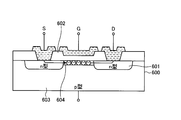
- FIG. 2 is a schematic cross-sectional view showing a schematic structure of a MOSFET used in the converter 3 of the first embodiment.
- FIG. 2 illustrates an n-type MOSFET.
- a p-type semiconductor substrate 600 is used, as shown in FIG.
- a source electrode S, a drain electrode D, and a gate electrode G are formed on the semiconductor substrate 600.
- High-concentration impurities are ion-implanted into the portions in contact with the source electrode S and the drain electrode D to form an n-type region 601.
- an oxide insulating film 602 is formed between the portion where the n-type region 601 is not formed and the gate electrode G. That is, an oxide insulating film 602 is interposed between the gate electrode G and the p-type region 603 of the semiconductor substrate 600.
- Channel 604 is an n-type channel in the example of FIG.
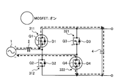
- FIG. 3 is a first diagram showing a path of a current flowing through the converter 3 in the first embodiment.
- FIG. 3 shows a state in which the power supply voltage polarity is positive and the absolute value of the detected value Is of the power supply current is larger than the current threshold value.
- the first upper arm element 311 and the second lower arm element 322 are on, and the first lower arm element 312 and the second upper arm element 321 are off.
- the current flows in the order of the AC power supply 1, the reactor 2, the switching element Q1, the smoothing capacitor 4, the switching element Q4, and the AC power supply 1.
- the first embodiment has an operation mode in which a current is passed through each channel of the switching elements Q1 and Q4 instead of passing a current through the diode D1 and the diode D4.
- This operation is called "synchronous rectification".
- FIG. 3 the MOSFETs that are turned on are indicated by circles. The same applies to the following figures. The details of the operation mode will be described later.
- FIG. 4 is a second diagram showing the path of the current flowing through the converter 3 in the first embodiment.
- FIG. 4 shows a state in which the power supply voltage polarity is negative and the absolute value of the detected value Is of the power supply current is larger than the current threshold value.
- the first lower arm element 312 and the second upper arm element 321 are on, and the first upper arm element 311 and the second lower arm element 322 are off.
- the current flows in the order of the AC power supply 1, the switching element Q3, the smoothing capacitor 4, the switching element Q2, the reactor 2, and the AC power supply 1.
- the synchronous rectification operation in which the current is passed through each channel of the switching elements Q3 and Q2 may be performed instead of passing the current through the diode D3 and the diode D2.
- FIG. 5 is a third diagram showing the path of the current flowing through the converter 3 in the first embodiment.
- FIG. 5 shows a state in which the power supply voltage polarity is positive and the absolute value of the detected value Is of the power supply current is larger than the current threshold value.
- the first lower arm element 312 and the second lower arm element 322 are on, and the first upper arm element 311 and the second upper arm element 321 are off.
- the current flows in the order of the AC power supply 1, the reactor 2, the switching element Q2, the switching element Q4, and the AC power supply 1.
- a power supply short-circuit path that does not pass through the smoothing capacitor 4 is formed.
- a mode is prepared in which a power short-circuit path is formed by passing a current through the channel of the switching element Q4 instead of passing a current through the diode D4.
- FIG. 6 is a fourth diagram showing the path of the current flowing through the converter 3 in the first embodiment.
- FIG. 6 shows a state in which the power supply voltage polarity is negative and the absolute value of the detected value Is of the power supply current is larger than the current threshold value.
- the first upper arm element 311 and the second upper arm element 321 are on, and the first lower arm element 312 and the second lower arm element 322 are off.
- the current flows in the order of the AC power supply 1, the switching element Q3, the switching element Q1, the reactor 2, and the AC power supply 1.
- a power supply short-circuit path that does not pass through the smoothing capacitor 4 is formed.
- a mode is prepared in which a power short-circuit path is formed by passing a current through the channel of the switching element Q3 instead of passing a current through the diode D3.
- the control unit 10 can control the values of the power supply current and the bus voltage by controlling the switching of the current path described above.
- the motor drive device 100 continuously switches between the operation shown in FIG. 3 and the operation shown in FIG.
- the power supply voltage polarity is negative
- the motor drive device 100 continuously switches between the operation shown in FIG. 4 and the operation shown in FIG.
- FIG. 7 is a diagram illustrating the characteristics of the operation mode according to the first embodiment.
- FIG. 8 is a diagram showing an operation waveform when operated in the operation mode shown in FIG. 7.
- FIG. 7 shows four operation modes: (a) rectification mode, (b) synchronous rectification mode, (c) low-speed switching mode, and (d) high-speed switching mode.
- Each operation mode is classified according to the combination of whether or not three controls, synchronous rectification, current control, and bus voltage control, are implemented. Synchronous rectification is as described above and is performed to improve operating efficiency.
- the bus voltage control is a control that suppresses an increase in the bus voltage.
- the current control is a control for improving the power factor of the current flowing in and out of the converter 3 and suppressing harmonics.
- the low-speed switching mode may be referred to as a "first switching mode”
- the high-speed switching mode may be referred to as a "second switching mode".
- the DC power supply device 50 has a rectification mode, and further has at least one operation mode of a synchronous rectification mode, a low-speed switching mode, and a high-speed switching mode.
- a low-speed switching mode in applications or products that do not require boosting operation, it may not be necessary to have a low-speed switching mode and a high-speed switching mode.
- FIG. 8A shows an operating waveform when operated in the rectified mode. Specifically, the waveforms of the control signals S321 to S322 for controlling the power supply voltage, the power supply current, and the switching elements Q1 to Q4 are shown from the upper side. The same applies to other operation modes.
- the rectification mode since it is not necessary to control the switching element, there is an advantage that the consumption of the power supply circuit 14 for operating the gate drive circuit 15 can be suppressed. Further, since it is not necessary to control the switching element, there is an advantage that the control is easy.
- FIG. 8B shows an operation waveform when operated in the synchronous rectification mode.
- the synchronous rectification mode is an operation mode in which the corresponding switching element is turned on at the timing of flowing through the parasitic diode and is passed through to the channel side of the switching element.
- the switching elements Q1 and Q4 or the switching elements Q2 and Q3 are turned on at the timing of flowing through the parasitic diode.
- the passing element is simply replaced with a switching element from the parasitic diode. Therefore, as shown in FIG. 7, current control and bus voltage control are not performed.
- FIG. 8C shows the operation waveform when operated in the low-speed switching mode.
- the low-speed switching mode is an operation mode in which the power supply voltage is short-circuited via the reactor 2 at least once every half cycle of the power supply voltage.
- the short-circuit operation is performed twice every half cycle of the power supply voltage.
- the boost amount of the bus voltage is adjusted by the bus voltage control.
- a proportional integration controller or the like is used for bus voltage control.
- the operation of the converter 3 is controlled so that the detected value Vdc of the bus voltage approaches the target voltage.
- the short-circuit time when the power supply voltage is short-circuited via the reactor 2 is controlled.
- the response time of the proportional integration controller it is possible to suppress an excessive increase in the bus voltage that may occur due to the occurrence of load fluctuation.
- a short-circuit current can be passed by short-circuit operation.
- the power factor can be improved and the harmonic current can be suppressed by expanding the flow width of the power supply current.
- the timing for performing the short-circuit operation may be determined in advance with reference to the zero crossing point of the power supply voltage, and may be referred to according to the load.
- the power supply current may be detected and the short circuit time may be controlled so that the detected current waveform approaches a sine wave.
- the short-circuit operation time since the short-circuit operation time is short, it is possible to suppress the generation of harmonic noise.
- FIG. 8D shows an operation waveform when operated in the high-speed switching mode.
- the high-speed switching mode is an operation mode in which the power supply voltage is short-circuited a plurality of times via the reactor 2 over the entire range of one cycle of the power supply voltage.
- the significance of short-circuit operation is the same as in the low-speed switching mode. That is, energy is stored in the reactor 2 by performing the short-circuit operation, and the energy stored in the reactor 2 is transferred to the smoothing capacitor 4 by releasing the short-circuit operation after the energy is stored. This makes it possible to boost the bus voltage.
- the control of the boost amount of the bus voltage can also be realized by the same control as in the low speed switching mode.
- the short-circuit operation is performed over the entire range of one cycle of the power supply voltage, so that the current flow width is wider than in the low-speed switching mode.
- the power factor can be controlled to a value close to 1.
- the load can be driven to the limit of the breaker capacity, especially on the high load side, and the power of the device can be increased.
- FIG. 9 is a diagram showing the loss characteristics of the MOSFET used in the DC power supply device 50 according to the first embodiment.
- the horizontal axis shows the current flowing through the MOSFET in the on state and the current flowing through the parasitic diode.
- the vertical axis shows the voltage required to pass a current through the switching element in the on state and the voltage required to pass a current through the parasitic diode.
- the solid line K1 represents the forward voltage of the parasitic diode.
- the parasitic diode forward voltage is an example of a current-voltage characteristic that represents the loss that occurs in a parasitic diode.
- a diode requires a large voltage because the loss is large when the current value is small, but when the current value is larger than a certain value, the rate of change of the loss is improved and the slope of the current-voltage characteristic is relaxed. .. This characteristic appears in the waveform shown by the solid line K1 in FIG.
- the broken line K2 represents the MOSFET drain-source voltage, which is the voltage between the MOSFET drain and the source.
- the MOSFET drain-source voltage is an example of a current-voltage characteristic that represents a current flowing through a carrier of a switching element and a loss caused by the on-resistance of the switching element due to the current flowing.
- a switching element such as a MOSFET
- the voltage required to pass a current increases in a quadratic curve with respect to the current value. This characteristic appears in the waveform shown by the broken line K2 in FIG.
- the cross point where the solid line K1 and the broken line K2 intersect is the current flowing through the parasitic diode and the voltage required to flow the current, the current flowing through the MOSFET and the voltage required to flow the current. Is the point at which is equal.
- the current value at the cross point where the two current-voltage characteristics of the parasitic diode and the switching element intersect is defined as the “second current threshold”.
- the above-mentioned current threshold value that is, the current threshold value used when comparing the absolute value of the detected value Is of the power supply current is referred to as a "first current threshold value”.
- the second current threshold value is represented by “Ith2”.
- the second current threshold is a value larger than the first current threshold.
- FIG. 10 is a diagram showing the timing at which the control unit 10 turns on the switching element in the DC power supply device 50 according to the first embodiment.
- the horizontal axis is time.
- the waveforms of the power supply voltage and the power supply current are shown in the upper part of FIG.
- switching elements Q1 and Q2 are current-synchronized switching elements whose on / off is controlled according to the polarity of the power supply current, and switching elements Q3 and Q4 are turned on / off according to the polarity of the power supply voltage.
- FIG. 10 shows the values of the first current threshold value Is1 and the second current threshold value Is2 together with the waveform of the power supply current.
- FIG. 10 shows one cycle of AC power output from the AC power source 1, the control unit 10 shall perform the same control as the control shown in FIG. 10 in other cycles.
- the control unit 10 When the power supply voltage polarity is positive, the control unit 10 turns on the switching element Q4 and turns off the switching element Q3. Further, when the power supply voltage polarity is negative, the control unit 10 turns on the switching element Q3 and turns off the switching element Q4.
- the timing at which the switching element Q4 is turned from on to off and the timing at which the switching element Q3 is turned from off to on are the same timing, but the timing is not limited to this.
- the control unit 10 may provide a dead time during which the switching elements Q3 and Q4 are both turned off between the timing at which the switching element Q4 is turned from on to off and the timing at which the switching element Q3 is turned from off to on.
- the control unit 10 provides a dead time during which the switching elements Q3 and Q4 are both turned off between the timing at which the switching element Q3 is turned from on to off and the timing at which the switching element Q4 is turned from off to on. May be good.
- the control unit 10 When the power supply voltage polarity is positive, the control unit 10 turns on the switching element Q1 when the absolute value of the power supply current becomes equal to or higher than the first current threshold value Is1. Further, when the absolute value of the power supply current exceeds the second current threshold value Is2, the switching element Q1 is turned off. After that, the control unit 10 turns on the switching element Q1 when the absolute value of the power supply current becomes small and the absolute value of the power supply current becomes equal to or less than the second current threshold value Is2. Further, when the absolute value of the power supply current becomes smaller than the first current threshold value Is1, the switching element Q1 is turned off.
- the control unit 10 turns on the switching element Q2 when the absolute value of the power supply current becomes equal to or higher than the first current threshold value Is1. Further, when the absolute value of the power supply current exceeds the second current threshold value Is2, the switching element Q2 is turned off. After that, the control unit 10 turns on the switching element Q2 when the absolute value of the power supply current becomes small and the absolute value of the power supply current becomes equal to or less than the second current threshold value Is2. Further, when the absolute value of the power supply current becomes smaller than the first current threshold value Is1, the switching element Q2 is turned off.
- the control unit 10 controls so that the switching elements Q1 and Q3 do not turn on at the same time, and controls the switching elements Q2 and Q4 not to turn on at the same time. .. As a result, the control unit 10 can prevent a capacitor short circuit in the motor drive device 100.
- the motor drive device 100 can realize synchronous rectification by the switching elements Q1 and Q2 of the first leg 31. Specifically, when the absolute value of the power supply current is equal to or greater than the first current threshold value Is1 and equal to or less than the second current threshold value Is2, the control unit 10 supplies a current to the switching element Q1 or the switching element Q2 having a small loss in this range. Shed. Further, when the absolute value of the power supply current is larger than the second current threshold value Is2, the control unit 10 causes a current to flow through the diode D1 or the diode D2 having a small loss in this range. As a result, the motor drive device 100 can pass a current through an element having a small loss according to the current value, so that a decrease in efficiency can be suppressed and a highly efficient device with reduced loss can be obtained.
- control unit 10 may perform a boosting operation by performing switching control in which the switching elements Q1 and Q2 are complementarily turned on and off during the period in which the switching element Q1 is turned on.
- control unit 10 may perform a boosting operation by performing switching control in which the switching elements Q1 and Q2 are complementarily turned on and off during the period in which the switching element Q2 is turned on.
- the control unit 10 when the absolute value of the power supply current is equal to or higher than the first current threshold value Is1 and equal to or lower than the second current threshold value Is2, the control unit 10 has the first leg 31 and the second leg according to the polarity of the power supply current.
- the switching element of one of the switching elements Q1 and Q2 constituting the first leg 31 of one of the 32 is allowed to be turned on.
- the control unit 10 when the absolute value of the power supply current is smaller than the first current threshold value Is1 or larger than the second current threshold value Is2, the control unit 10 is the same one switching element as the above-mentioned switching elements Q1 and Q2. Prohibit turning on.
- the control unit 10 turns on the switching element Q1. Allow. When the absolute value of the power supply current is smaller than the first current threshold value Is1 or larger than the second current threshold value Is2, the switching element Q1 is prohibited from being turned on. When the polarity of the power supply current is positive and the absolute value of the power supply current is equal to or greater than the first current threshold value Is1 and equal to or less than the second current threshold value Is2, the control unit 10 switches the switching element Q1 during the off period. Turn on Q2. When the absolute value of the power supply current is smaller than the first current threshold value Is1 or larger than the second current threshold value Is2, turning on the switching element Q2 is also prohibited.
- control unit 10 permits the switching element Q2 to be turned on when the polarity of the power supply current is negative and the absolute value of the power supply current is equal to or higher than the first current threshold value Is1 and equal to or lower than the second current threshold value Is2. .. When the absolute value of the power supply current is smaller than the first current threshold value Is1 or larger than the second current threshold value Is2, the switching element Q2 is prohibited from being turned on. Further, when the polarity of the power supply current is negative and the absolute value of the power supply current is equal to or higher than the first current threshold value Is1 and equal to or lower than the second current threshold value Is2, the control unit 10 is in the period when the switching element Q2 is off. The switching element Q1 is turned on. When the absolute value of the power supply current is smaller than the first current threshold value Is1 or larger than the second current threshold value Is2, the switching element Q1 is also prohibited from being turned on.
- control unit 10 allows the switching element to be turned on in a region where the absolute value of the power supply current is equal to or higher than the first current threshold value Is1 and the loss of the switching element is smaller than the loss of the parasitic diode. Further, the control unit 10 prohibits the switching element from being turned on in a region where the loss of the switching element is larger than the loss of the parasitic diode.
- control unit 10 controls the on / off of the switching elements Q3 and Q4 according to the polarity of the power supply voltage, and controls the on / off of the switching elements Q1 and Q2 according to the polarity of the power supply current.
- the control unit 10 may control the on / off of the switching elements Q1 and Q2 according to the polarity of the power supply voltage, and may control the on / off of the switching elements Q3 and Q4 according to the polarity of the power supply current.
- the second current threshold value Is2 is, as described above, a current value when the voltage required for passing the current through the parasitic diode and the switching element becomes the same value, but is not limited to this.
- the second current threshold value Is2 may be a value determined according to the characteristics of the voltage required to pass a current through the parasitic diode and the characteristics of the voltage required to pass a current through the switching element.
- the second current threshold value Is2 is set to be larger than the current value when the voltage required to pass the current through the parasitic diode and the switching element becomes the same value according to the switching loss generated in the switching element. It may be a value. Thereby, it is possible to determine the second current threshold value Is2 in consideration of the switching element generated when the switching element is switched from on to off. In this case, the control unit 10 keeps the switching element on when the loss cannot be reduced by turning off the switching element even if the absolute value of the power supply current becomes larger while the switching element is on. To. As a result, the motor drive device 100 can further suppress a decrease in efficiency.
- the second current threshold value Is2 may be a value obtained by adding or subtracting a specified value with respect to the current value when the voltage required for passing the current through the parasitic diode and the switching element becomes the same value. ..
- the second current threshold value Is2 can be determined in consideration of the difference in characteristics due to the variation in the components of each element.
- the control unit 10 improves the reduction of loss as compared with the case where the second current threshold value Is2 is the current value when the voltage required for passing the current through the parasitic diode and the switching element becomes the same value. It may not be possible. However, the control unit 10 can reduce the loss as compared with the case where the switching element is continuously turned on even if the absolute value of the power supply current becomes larger in the state where the switching element is turned on.
- FIG. 11 is a flowchart used for explaining the operation of the main part in the first embodiment.
- FIG. 11 shows a processing flow in which the control unit 10 of the motor drive device 100 controls the switching elements Q1 and Q2 on and off.
- the control unit 10 of the motor drive device 100 controls the switching elements Q1 and Q2 on and off.
- the control unit 10 compares the absolute value
- step S23 When the absolute value
- step S21 described above the case where the absolute value
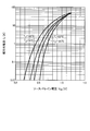
- FIG. 12 is a diagram showing the temperature characteristics of the forward current of the parasitic diode in a general MOSFET.
- FIG. 13 is a diagram showing the temperature characteristics of the on-resistance of a general MOSFET.
- FIG. 14 is a diagram showing how the cross point shown in FIG. 9 fluctuates depending on the temperature.
- the solid line K1 indicates the solid line K1 shown in FIG. 9
- the broken line K2 indicates the broken line K2 shown in FIG.
- the on-resistance R DS of a typical MOSFET, as shown in FIG. 13, for the same drain current I D, transitioning to the direction of increasing the higher the temperature T a is.
- the dashed line K2 shown in FIG. 14 the temperature T a is increased, moves to the plane of the upper left direction as shown by a broken line K2 '.
- the second current threshold value Is2 which is the current value at the cross point, moves to the left side of the paper, that is, in the direction in which the current value decreases as the temperature rises.
- the second current threshold value Is2 and the second current threshold value Is2'in FIG. 14 are in the range in which synchronous rectification is performed, but synchronous rectification is not performed. The loss is smaller and the efficiency is higher. Therefore, if the second current threshold value Is2 in the flowchart of FIG. 11 is corrected based on the ambient temperature of the switching element or the outside air temperature of the device on which the switching element is mounted, the efficiency of the DC power supply device 50 can be further improved. It becomes possible to increase.
- one of the methods for increasing the switching speed of the switching element is a method for reducing the gate resistance of the switching element. As the gate resistance becomes smaller, the charge / discharge time to the gate input capacitance becomes shorter, and the turn-on period and the turn-off period become shorter, so that the switching speed becomes faster.
- the switching element is composed of a WBG semiconductor such as GaN or SiC.
- a WBG semiconductor for the switching element By using a WBG semiconductor for the switching element, the loss per switching can be further suppressed, the efficiency is further improved, and high frequency switching becomes possible. Further, by enabling high-frequency switching, the reactor 2 can be miniaturized, and the motor drive device 100 can be miniaturized and lightened. Further, by using the WBG semiconductor for the switching element, the switching speed is improved and the switching loss is suppressed. This makes it possible to simplify heat dissipation measures so that the switching element can continue to operate normally. Further, by using a WBG semiconductor for the switching element, the switching frequency can be set to a sufficiently high value, for example, 16 kHz or more. As a result, noise caused by switching can be suppressed.
- the audible range frequency is in the range of 16 kHz to 20 kHz, that is, in the range of 266 to 400 times the frequency of the commercial power supply.
- GaN semiconductors are suitable for switching at frequencies higher than this audible frequency.
- the switching elements Q1 to Q4 made of the GaN semiconductor have a very small switching loss even when driven at a switching frequency of several tens of kHz or more, specifically, a switching frequency higher than 20 kHz. Therefore, heat dissipation measures are not required, or the size of the heat dissipation member used for heat dissipation measures can be reduced, and the motor drive device 100 can be made smaller and lighter. Further, since high frequency switching is possible, the reactor 2 can be miniaturized.
- the switching frequency is preferably 150 kHz or less in order to prevent the primary component of the switching frequency from entering the measurement range of the noise terminal voltage standard.
- the WBG semiconductor since the WBG semiconductor has a smaller capacitance than the Si semiconductor, the generation of recovery current due to switching is small, and the generation of loss and noise due to recovery current can be suppressed. Therefore, the WBG semiconductor is suitable for high frequency switching.
- the on-resistance of SiC semiconductors is smaller than that of GaN semiconductors. Therefore, the first upper arm element 311 and the first lower arm element 312 of the first leg 31 having a larger number of switching times than the second leg 32 are made of a GaN semiconductor, and the second leg element 312 has a smaller number of switching times.
- the second upper arm element 321 and the second lower arm element 322 of the leg 32 may be made of a SiC semiconductor. As a result, the characteristics of the SiC semiconductor and the GaN semiconductor can be fully utilized.
- the SiC semiconductor for the second upper arm element 321 and the second lower arm element 322 of the second leg 32 which has fewer switching times than the first leg 31, the second upper arm Of the losses of the element 321 and the second lower arm element 322, the conduction loss accounts for a large proportion, and the turn-on loss and the turn-off loss become small. Therefore, the increase in heat generation due to the switching of the second upper arm element 321 and the second lower arm element 322 is suppressed, and the second upper arm element 321 and the second lower arm element constituting the second leg 32 are suppressed.
- the chip area of 322 can be made relatively small. This makes it possible to effectively utilize a SiC semiconductor having a low yield at the time of chip manufacturing.
- an SJ-MOSFET having a super junction structure may be used for the second upper arm element 321 and the second lower arm element 322 of the second leg 32 having a small number of switchings.
- SJ-MOSFET it is possible to suppress the demerit that the capacitance is high and recovery is likely to occur while taking advantage of the low on-resistance which is the merit of SJ-MOSFET.
- the manufacturing cost of the second leg 32 can be reduced as compared with the case of using the WBG semiconductor.
- WBG semiconductors have higher heat resistance than Si semiconductors and can operate even at high junction temperatures. Therefore, by using the WBG semiconductor, the first leg 31 and the second leg 32 can be configured by a small chip having a large thermal resistance.
- SiC semiconductors which have a low yield during chip manufacturing, can be used for small chips to reduce costs.
- the WBG semiconductor suppresses the increase in the loss generated in the switching element even when driven at a high frequency of about 100 kHz, the loss reduction effect due to the miniaturization of the reactor 2 becomes large, and a wide output band, that is, a wide load Under the conditions, a highly efficient converter can be realized.
- the WBG semiconductor has higher heat resistance than the Si semiconductor and has a high heat generation allowable level for switching due to the bias of the loss between the arms, so that it is suitable for the first leg 31 in which the switching loss due to high frequency driving occurs.
- the voltage detection unit 7 which is the first physical quantity detection unit detects the bus voltage which is the first physical quantity which represents the operating state of the output side of the converter 3.
- the first and second physical quantities are input to the control unit 10.
- the control unit 10 controls the operation of the converter 3 based on the first and second physical quantities.
- the control unit 10 further controls the continuity of each switching element of the converter 3 in response to the ambient temperature of the switching element, the outside air temperature of the converter, or the operation command to the converter 3, and operates the converter 3 in different operation modes. It has multiple modes. As a result, further efficiency can be achieved when applying synchronous rectification.
- the control unit 10 when the absolute value of the power supply current is equal to or more than the first current threshold value and equal to or less than the second current threshold value, the control unit 10 has a switching element having a smaller loss than the parasitic diode in this range. Allow to turn on. Further, when the absolute value of the power supply current is larger than the second current threshold value, the control unit 10 prohibits turning on the switching element having a larger loss than the parasitic diode in this range. As a result, in the converter 3, a current can be passed through an element having a small loss according to the current value. As a result, it is possible to obtain a highly efficient DC power supply device 50 with reduced efficiency and loss. In this control, it is preferable that the second current threshold value is corrected based on the ambient temperature of the switching element or the outside air temperature of the device on which the switching element is mounted. As a result, a more efficient DC power supply device 50 can be obtained.
- FIG. 15 is a block diagram showing an example of a hardware configuration that embodies the function of the control unit 10 according to the first embodiment.
- FIG. 16 is a block diagram showing another example of a hardware configuration that embodies the function of the control unit 10 according to the first embodiment.
- the processor 300 that performs the calculation
- the memory 302 that stores the program read by the processor 300
- the input / output of the signal are input / output. It can be configured to include the interface 304 to be performed.
- the processor 300 may be an arithmetic unit, a microprocessor, a microcomputer, a CPU (Central Processing Unit), or a DSP (Digital Signal Processor).
- the memory 302 includes a non-volatile or volatile semiconductor memory such as a RAM (Random Access Memory), a ROM (Read Only Memory), a flash memory, an EPROM (Erasable Program ROM), and an EPROM (registered trademark) (Electrically EPROM). Examples thereof include magnetic disks, flexible disks, optical disks, compact disks, mini disks, and DVDs (Digital entirely Disc).
- the memory 302 stores a program that executes the function of the control unit 10 according to the first embodiment.
- the processor 300 sends and receives necessary information via the interface 304, the processor 300 executes a program stored in the memory 302, and the processor 300 refers to a table stored in the memory 302 to perform the above-described processing. It can be carried out.
- the calculation result by the processor 300 can be stored in the memory 302.
- the processing circuit 305 shown in FIG. 16 can also be used.
- the processing circuit 305 corresponds to a single circuit, a composite circuit, an ASIC (Application Specific Integrated Circuit), an FPGA (Field-Programmable Gate Array), or a combination thereof.
- the information input to the processing circuit 305 and the information output from the processing circuit 305 can be obtained via the interface 306. Even in the configuration using the processing circuit 305, some processing in the control unit 10 may be performed by the processor 300 having the configuration shown in FIG.
- Embodiment 2 control will be described when the gate drive circuit 15 for driving each switching element of the converter 3 includes a bootstrap circuit.
- FIG. 17 is a diagram showing a configuration example of the gate drive circuit 15 according to the second embodiment.
- the gate drive circuit 15 includes drive circuits 51 and 52 and a bootstrap circuit 54.
- the drive circuit 51 is a drive circuit used when driving the first upper arm element 311 of the first leg 31.
- the drive circuit 52 is a drive circuit used when driving the first lower arm element 312 of the first leg 31.
- the second upper arm element 321 and the second lower arm element 322 of the second leg 32 are also driven by two similar drive circuits.
- the bootstrap circuit 54 includes a resistor 54a, a diode 54b, and a capacitor 54c which is a bootstrap capacitor.
- a drive voltage is applied to the capacitor 54c from the drive power supply 55 via a series circuit of the resistor 54a and the diode 54b.
- the charging voltage of the capacitor 54c is a gate drive voltage for driving the switching elements Q1 and Q3 of the upper arm.
- the gate drive voltage for driving the switching elements Q1 and Q3 of the upper arm turns on the switching elements Q2 and Q4 of the lower arm. Obtained by letting. If the control signals S311 to S322 as shown in FIG. 8 are used, it is possible to reliably generate a gate drive voltage for driving the switching element of the upper arm.
- FIG. 18 is a diagram showing an operation waveform in the second embodiment corresponding to FIG.
- FIG. 18 shows an operation waveform in which a part of the control signals S311 to S322 is changed in the operation mode shown in FIG.
- the differences between the operation waveform shown in FIG. 18 and the operation waveform shown in FIG. 8 are as follows.
- each switching element does not operate on, so the operating waveform is the same.
- the operating waveform is the same even in the synchronous rectification mode.
- FIG. 8 (c) is changed as shown in FIG. 18 (c). Also in FIG. 18C, since the switching elements Q1 and Q3 of the upper arm do not operate, the loss in the bootstrap circuit 54 is reduced. As for the high-speed switching mode, as can be seen from the comparison between FIGS. 8 (d) and 18 (d), the operating waveforms are the same. With reference to FIG. 8D, it can be seen that the switching elements Q1 and Q3 of the upper arm are not operating, and the loss in the bootstrap circuit 54 is reduced by the original operating waveform. Whether to select the switching pattern of FIG. 8 or the switching pattern of FIG. 18 is determined based on the load condition. The details of the load condition will be described in the third embodiment described later.
- the gate drive circuit 15 which is a drive circuit for driving the converter 3 drives the switching elements Q1 and Q3 of the upper arm connected to the positive side of the smoothing capacitor 4.
- a bootstrap circuit 54 which is a drive power source for the device, is provided.
- the control unit 10 has a low-speed switching mode as an operation mode, and when operating in the low-speed switching mode, the control unit 10 stops the operation of the switching element connected to the bootstrap circuit 54 based on the load condition. As a result, the DC power supply device 50 can be efficiently operated in the configuration including the bootstrap circuit 54.
- the gate drive circuit 15 which is a drive circuit for driving the converter 3 is a drive power source for driving the switching elements Q1 and Q3 of the upper arm connected to the positive side of the smoothing capacitor 4.
- the bootstrap circuit 54 is provided.
- the control unit 10 has a high-speed switching mode as an operation mode, and in the high-speed switching mode, the switching element connected to the bootstrap circuit 54 does not operate on. As a result, the DC power supply device 50 can be efficiently operated in the configuration including the bootstrap circuit 54.
- Embodiment 3 an application example of the motor drive device 100 described in the first embodiment will be described.
- FIG. 19 is a diagram showing the configuration of the air conditioner 400 according to the third embodiment.
- the motor drive device 100 described in the first embodiment and the second embodiment can be applied to products such as a blower, a compressor, and an air conditioner.
- an example in which the motor drive device 100 is applied to the air conditioner 400 will be described as an application example of the motor drive device 100 according to the first embodiment and the second embodiment.
- a motor 500 is connected to the output side of the motor drive device 100, and the motor 500 is connected to the compression element 504.
- the compressor 505 includes a motor 500 and a compression element 504.
- the refrigeration cycle unit 506 is configured to include a four-way valve 506a, an indoor heat exchanger 506b, an expansion valve 506c, and an outdoor heat exchanger 506d.
- the flow path of the refrigerant circulating inside the air conditioner 400 is from the compression element 504 via the four-way valve 506a, the indoor heat exchanger 506b, the expansion valve 506c, the outdoor heat exchanger 506d, and again via the four-way valve 506a. Therefore, it is configured to return to the compression element 504.
- the motor drive device 100 receives AC power from the AC power source 1 and rotates the motor 500.
- the compression element 504 executes a compression operation of the refrigerant by rotating the motor 500, and the refrigerant can be circulated inside the refrigeration cycle unit 506.
- the air conditioner 400 In the air conditioner 400, operation under intermediate conditions where the output is less than half of the rated output, that is, under low output conditions is dominant throughout the year. Therefore, the contribution to annual power consumption is high under intermediate conditions. Further, in the air conditioner 400, the rotation speed of the motor 500 tends to be low, and the bus voltage required to drive the motor 500 tends to be low. Therefore, it is effective from the viewpoint of system efficiency that the switching element used in the air conditioner 400 is operated in a passive state. Therefore, the DC power supply device 50 capable of reducing loss in a wide range of operation modes from the passive state to the high frequency switching state is useful for the air conditioner 400.
- the DC power supply device 50 can suppress the switching loss, the temperature rise of the DC power supply device 50 is suppressed, and even if the size of the outdoor unit blower (not shown) is reduced, the substrate mounted on the DC power supply device 50 Cooling capacity can be secured. Therefore, the DC power supply device 50 is suitable for an air conditioner 400 having high efficiency and a high output of 4.0 kW or more.
- the switching loss is reduced, the energy consumption rate is low, and the highly efficient air conditioner 400 can be realized by driving the switching element at a high frequency.
- FIG. 20 is a diagram showing the characteristics of the operation mode according to the third embodiment.
- FIG. 20 shows an operation mode corresponding to the temperature condition and the load condition when the air conditioner 400 is operated, and the operation of the switching element of the upper arm when the air conditioner 400 is operated in the operation mode.
- the air conditioner 400 is not operating stably in terms of control at the time of startup and at the time of abnormality.
- An example of the temperature condition of the air conditioner is the outside air temperature of the device on which the switching element is mounted.
- the cooling operation is used when the outside air temperature is high.
- this cooling operation there are load conditions such as intermediate cooling, cooling rating, and cooling overload.
- the outside air temperature is high, the ambient temperature of the switching element also tends to be high.
- the loss in the diode is obtained by the product of the forward current and the forward voltage drop, which is the forward voltage drop due to the forward current. Further, the loss of the MOSFET is obtained by the square of the current flowing through the MOSFET with the on-resistance of the MOSFET. Further, as described above, the diode tends to have a lower forward voltage drop as the temperature rises, and the MOSFET tends to have a higher on-resistance as the temperature rises. In other words, the loss of a diode improves as the temperature rises, and the loss of a MOSFET worsens as the temperature rises.
- the bootstrap circuit 54 described above is widely used.
- a loss occurs in the drive circuit 51 that drives the MOSFET of the upper arm, and the loss of the drive circuit 51 increases in proportion to the number of switchings for switching and controlling the MOSFET. Therefore, depending on the load conditions, it is assumed that the loss of the parasitic diode is smaller than the loss including the loss of the MOSFET of the upper arm and the loss of the drive circuit 51. In particular, when the ambient temperature of the converter 3 is high and the current is large, the effect is remarkable. Therefore, the switching operation of the MOSFET of the upper arm is stopped, and the operation mode is set in consideration of the control of positively conducting the parasitic diode.
- the ambient temperature of the switching element is also high.
- the temperature of the switching element itself may rise due to heat generation, especially in the low-speed switching mode and high-speed switching mode in which the current becomes large, the operation of the switching element of the upper arm is stopped and the diode is conducted to conduct the operation efficiency. To improve.
- the synchronous rectification mode in which the switching element of the upper arm is operated is selected in the middle of cooling, which is a light load.
- a low-speed switching mode in which the switching element of the upper arm is not operated is selected in the cooling rating with a high load.
- a high-speed switching mode in which the switching element of the upper arm is not operated is selected in the cooling overload.
- the ambient temperature of the switching element is also lower than during the cooling operation. Therefore, during the heating operation, synchronous rectification by operating the switching element of the upper arm is positively performed to improve the operation efficiency.
- the synchronous rectification mode in which the switching element of the upper arm is operated is selected in the heating intermediate where the load is light.
- the low speed switching mode in which the switching element of the upper arm is operated is selected.
- the heating overload which is an overload
- a high-speed switching mode in which the switching element of the upper arm is operated is selected. That is, the operation mode in which the switching element of the upper arm is operated is selected in any of the heating intermediate with a light load, the heating rating with a high load, and the heating overload with an overload.
- the continuity of the switching element of the converter 3 is controlled in response to an operation command to the converter 3 such as cooling operation or heating operation, specifically, cooling intermediate or heating intermediate.
- an operation command to the converter 3 such as cooling operation or heating operation, specifically, cooling intermediate or heating intermediate.
- the dead time is a non-overlapping time in which the MOSFET of the upper arm and the MOSFET of the lower arm do not turn on at the same time, and is also called a short circuit prevention time. If the control does not provide a dead time, the consistency between the command value by the control and the actual command value is improved. As a result, the controllability is improved, and the air conditioner 400 with high efficiency and high control stability can be realized.
- FIGS. 12 and 13 in the MOSFET are the current characteristics and may be improved in the future. Therefore, the determination as to whether or not to operate the switching element of the upper arm may be flexibly performed according to the technological trend of the MOSFET, as shown in parentheses in FIG. 20.
Landscapes
- Engineering & Computer Science (AREA)
- Power Engineering (AREA)
- Rectifiers (AREA)
Priority Applications (2)
| Application Number | Priority Date | Filing Date | Title |
|---|---|---|---|
| JP2021541952A JP7162747B2 (ja) | 2019-08-30 | 2019-08-30 | 直流電源装置、モータ駆動装置、送風機、圧縮機及び空気調和機 |
| PCT/JP2019/034262 WO2021038868A1 (ja) | 2019-08-30 | 2019-08-30 | 直流電源装置、モータ駆動装置、送風機、圧縮機及び空気調和機 |
Applications Claiming Priority (1)
| Application Number | Priority Date | Filing Date | Title |
|---|---|---|---|
| PCT/JP2019/034262 WO2021038868A1 (ja) | 2019-08-30 | 2019-08-30 | 直流電源装置、モータ駆動装置、送風機、圧縮機及び空気調和機 |
Publications (1)
| Publication Number | Publication Date |
|---|---|
| WO2021038868A1 true WO2021038868A1 (ja) | 2021-03-04 |
Family
ID=74685390
Family Applications (1)
| Application Number | Title | Priority Date | Filing Date |
|---|---|---|---|
| PCT/JP2019/034262 Ceased WO2021038868A1 (ja) | 2019-08-30 | 2019-08-30 | 直流電源装置、モータ駆動装置、送風機、圧縮機及び空気調和機 |
Country Status (2)
| Country | Link |
|---|---|
| JP (1) | JP7162747B2 (https=) |
| WO (1) | WO2021038868A1 (https=) |
Cited By (2)
| Publication number | Priority date | Publication date | Assignee | Title |
|---|---|---|---|---|
| WO2025158852A1 (ja) * | 2024-01-26 | 2025-07-31 | 三菱重工サーマルシステムズ株式会社 | コンバータ装置及びその制御方法並びにプログラム |
| US12480527B2 (en) | 2022-10-07 | 2025-11-25 | Hamilton Sundstrand Corporation | High-power air-coooled compressor motor and low-power cooling booster fan motor powered by single inverter |
Citations (4)
| Publication number | Priority date | Publication date | Assignee | Title |
|---|---|---|---|---|
| JP2015012640A (ja) * | 2013-06-27 | 2015-01-19 | 株式会社デンソー | 電力変換装置 |
| JP2016220378A (ja) * | 2015-05-19 | 2016-12-22 | ジョンソンコントロールズ ヒタチ エア コンディショニング テクノロジー(ホンコン)リミテッド | 直流電源装置、並びにそれを用いる空気調和機 |
| JP2017055581A (ja) * | 2015-09-10 | 2017-03-16 | ジョンソンコントロールズ ヒタチ エア コンディショニング テクノロジー(ホンコン)リミテッド | 直流電源装置および空気調和機 |
| JP2017055475A (ja) * | 2015-09-07 | 2017-03-16 | ジョンソンコントロールズ ヒタチ エア コンディショニング テクノロジー(ホンコン)リミテッド | 直流電源装置および空気調和機 |
-
2019
- 2019-08-30 JP JP2021541952A patent/JP7162747B2/ja active Active
- 2019-08-30 WO PCT/JP2019/034262 patent/WO2021038868A1/ja not_active Ceased
Patent Citations (4)
| Publication number | Priority date | Publication date | Assignee | Title |
|---|---|---|---|---|
| JP2015012640A (ja) * | 2013-06-27 | 2015-01-19 | 株式会社デンソー | 電力変換装置 |
| JP2016220378A (ja) * | 2015-05-19 | 2016-12-22 | ジョンソンコントロールズ ヒタチ エア コンディショニング テクノロジー(ホンコン)リミテッド | 直流電源装置、並びにそれを用いる空気調和機 |
| JP2017055475A (ja) * | 2015-09-07 | 2017-03-16 | ジョンソンコントロールズ ヒタチ エア コンディショニング テクノロジー(ホンコン)リミテッド | 直流電源装置および空気調和機 |
| JP2017055581A (ja) * | 2015-09-10 | 2017-03-16 | ジョンソンコントロールズ ヒタチ エア コンディショニング テクノロジー(ホンコン)リミテッド | 直流電源装置および空気調和機 |
Cited By (2)
| Publication number | Priority date | Publication date | Assignee | Title |
|---|---|---|---|---|
| US12480527B2 (en) | 2022-10-07 | 2025-11-25 | Hamilton Sundstrand Corporation | High-power air-coooled compressor motor and low-power cooling booster fan motor powered by single inverter |
| WO2025158852A1 (ja) * | 2024-01-26 | 2025-07-31 | 三菱重工サーマルシステムズ株式会社 | コンバータ装置及びその制御方法並びにプログラム |
Also Published As
| Publication number | Publication date |
|---|---|
| JPWO2021038868A1 (https=) | 2021-03-04 |
| JP7162747B2 (ja) | 2022-10-28 |
Similar Documents
| Publication | Publication Date | Title |
|---|---|---|
| CN110915119B (zh) | 电力变换装置、电动机驱动装置以及空调机 | |
| JP7118284B2 (ja) | 直流電源装置、モータ駆動装置、送風機、圧縮機及び空気調和機 | |
| US11909299B2 (en) | Power converting apparatus, motor driving apparatus, and air conditioner | |
| JP6935022B2 (ja) | 電力変換装置、モータ駆動装置及び空気調和機 | |
| JP7162747B2 (ja) | 直流電源装置、モータ駆動装置、送風機、圧縮機及び空気調和機 | |
| JP7080381B2 (ja) | 電力変換装置、モータ駆動装置及び空気調和機 | |
| JP7101898B2 (ja) | モータ駆動装置、送風機、圧縮機及び空気調和機 | |
| CN114287104B (zh) | 电力变换装置、马达驱动装置以及空调机 | |
| JP7162746B2 (ja) | 直流電源装置、モータ駆動装置、送風機、圧縮機及び空気調和機 | |
| CN112740530B (zh) | 电力转换装置、电机驱动装置以及空调机 | |
| WO2020066034A1 (ja) | 電力変換装置、モータ駆動装置及び空気調和機 | |
| JP7325516B2 (ja) | 電力変換装置、モータ駆動装置及び空気調和機 | |
| JPWO2020246038A1 (ja) | モータ駆動装置、送風機、圧縮機及び空気調和機 |
Legal Events
| Date | Code | Title | Description |
|---|---|---|---|
| 121 | Ep: the epo has been informed by wipo that ep was designated in this application |
Ref document number: 19943051 Country of ref document: EP Kind code of ref document: A1 |
|
| ENP | Entry into the national phase |
Ref document number: 2021541952 Country of ref document: JP Kind code of ref document: A |
|
| NENP | Non-entry into the national phase |
Ref country code: DE |
|
| 122 | Ep: pct application non-entry in european phase |
Ref document number: 19943051 Country of ref document: EP Kind code of ref document: A1 |