WO2021029285A1 - Semiconductor device - Google Patents
Semiconductor device Download PDFInfo
- Publication number
- WO2021029285A1 WO2021029285A1 PCT/JP2020/029879 JP2020029879W WO2021029285A1 WO 2021029285 A1 WO2021029285 A1 WO 2021029285A1 JP 2020029879 W JP2020029879 W JP 2020029879W WO 2021029285 A1 WO2021029285 A1 WO 2021029285A1
- Authority
- WO
- WIPO (PCT)
- Prior art keywords
- peak
- concentration
- region
- semiconductor substrate
- semiconductor device
- Prior art date
Links
- 239000004065 semiconductor Substances 0.000 title claims abstract description 206
- 239000000758 substrate Substances 0.000 claims abstract description 134
- 229910052739 hydrogen Inorganic materials 0.000 claims description 39
- 239000001257 hydrogen Substances 0.000 claims description 39
- UFHFLCQGNIYNRP-UHFFFAOYSA-N Hydrogen Chemical compound [H][H] UFHFLCQGNIYNRP-UHFFFAOYSA-N 0.000 claims description 29
- 230000006798 recombination Effects 0.000 claims description 15
- 238000009826 distribution Methods 0.000 description 54
- 239000000386 donor Substances 0.000 description 42
- 230000005684 electric field Effects 0.000 description 31
- 239000000370 acceptor Substances 0.000 description 27
- 230000007547 defect Effects 0.000 description 18
- 239000011229 interlayer Substances 0.000 description 14
- 238000000034 method Methods 0.000 description 14
- 239000000126 substance Substances 0.000 description 14
- 238000010586 diagram Methods 0.000 description 13
- 239000012535 impurity Substances 0.000 description 13
- 239000010410 layer Substances 0.000 description 13
- 230000002093 peripheral effect Effects 0.000 description 12
- 230000000052 comparative effect Effects 0.000 description 11
- 229910052734 helium Inorganic materials 0.000 description 11
- 239000001307 helium Substances 0.000 description 11
- SWQJXJOGLNCZEY-UHFFFAOYSA-N helium atom Chemical compound [He] SWQJXJOGLNCZEY-UHFFFAOYSA-N 0.000 description 11
- -1 aluminum-silicon-copper Chemical compound 0.000 description 9
- 125000004429 atom Chemical group 0.000 description 9
- OAICVXFJPJFONN-UHFFFAOYSA-N Phosphorus Chemical compound [P] OAICVXFJPJFONN-UHFFFAOYSA-N 0.000 description 8
- 229910052698 phosphorus Inorganic materials 0.000 description 8
- 239000011574 phosphorus Substances 0.000 description 8
- 229910052782 aluminium Inorganic materials 0.000 description 7
- XAGFODPZIPBFFR-UHFFFAOYSA-N aluminium Chemical compound [Al] XAGFODPZIPBFFR-UHFFFAOYSA-N 0.000 description 7
- 239000002245 particle Substances 0.000 description 7
- 238000003860 storage Methods 0.000 description 7
- 239000000852 hydrogen donor Substances 0.000 description 6
- 229910052751 metal Inorganic materials 0.000 description 5
- 239000002184 metal Substances 0.000 description 5
- 230000004913 activation Effects 0.000 description 4
- 230000007423 decrease Effects 0.000 description 4
- 229910021420 polycrystalline silicon Inorganic materials 0.000 description 4
- 229920005591 polysilicon Polymers 0.000 description 4
- 230000015572 biosynthetic process Effects 0.000 description 3
- 239000002019 doping agent Substances 0.000 description 3
- 230000010355 oscillation Effects 0.000 description 3
- 239000011148 porous material Substances 0.000 description 3
- 230000003068 static effect Effects 0.000 description 3
- ZOXJGFHDIHLPTG-UHFFFAOYSA-N Boron Chemical compound [B] ZOXJGFHDIHLPTG-UHFFFAOYSA-N 0.000 description 2
- XUIMIQQOPSSXEZ-UHFFFAOYSA-N Silicon Chemical compound [Si] XUIMIQQOPSSXEZ-UHFFFAOYSA-N 0.000 description 2
- 238000009825 accumulation Methods 0.000 description 2
- 229910052785 arsenic Inorganic materials 0.000 description 2
- RQNWIZPPADIBDY-UHFFFAOYSA-N arsenic atom Chemical compound [As] RQNWIZPPADIBDY-UHFFFAOYSA-N 0.000 description 2
- QVGXLLKOCUKJST-UHFFFAOYSA-N atomic oxygen Chemical compound [O] QVGXLLKOCUKJST-UHFFFAOYSA-N 0.000 description 2
- 230000004888 barrier function Effects 0.000 description 2
- 229910052796 boron Inorganic materials 0.000 description 2
- 239000000969 carrier Substances 0.000 description 2
- 239000004020 conductor Substances 0.000 description 2
- 238000001514 detection method Methods 0.000 description 2
- 238000009792 diffusion process Methods 0.000 description 2
- 230000001747 exhibiting effect Effects 0.000 description 2
- 150000002431 hydrogen Chemical class 0.000 description 2
- 150000002500 ions Chemical class 0.000 description 2
- 238000004519 manufacturing process Methods 0.000 description 2
- 239000000463 material Substances 0.000 description 2
- 238000000691 measurement method Methods 0.000 description 2
- 229910001092 metal group alloy Inorganic materials 0.000 description 2
- 239000007769 metal material Substances 0.000 description 2
- 229910052760 oxygen Inorganic materials 0.000 description 2
- 239000001301 oxygen Substances 0.000 description 2
- 229910052710 silicon Inorganic materials 0.000 description 2
- 239000010703 silicon Substances 0.000 description 2
- 229910000881 Cu alloy Inorganic materials 0.000 description 1
- BUGBHKTXTAQXES-UHFFFAOYSA-N Selenium Chemical compound [Se] BUGBHKTXTAQXES-UHFFFAOYSA-N 0.000 description 1
- 229910000676 Si alloy Inorganic materials 0.000 description 1
- NINIDFKCEFEMDL-UHFFFAOYSA-N Sulfur Chemical compound [S] NINIDFKCEFEMDL-UHFFFAOYSA-N 0.000 description 1
- RTAQQCXQSZGOHL-UHFFFAOYSA-N Titanium Chemical compound [Ti] RTAQQCXQSZGOHL-UHFFFAOYSA-N 0.000 description 1
- KPSZQYZCNSCYGG-UHFFFAOYSA-N [B].[B] Chemical compound [B].[B] KPSZQYZCNSCYGG-UHFFFAOYSA-N 0.000 description 1
- CSDREXVUYHZDNP-UHFFFAOYSA-N alumanylidynesilicon Chemical compound [Al].[Si] CSDREXVUYHZDNP-UHFFFAOYSA-N 0.000 description 1
- 238000000137 annealing Methods 0.000 description 1
- 229910052787 antimony Inorganic materials 0.000 description 1
- WATWJIUSRGPENY-UHFFFAOYSA-N antimony atom Chemical compound [Sb] WATWJIUSRGPENY-UHFFFAOYSA-N 0.000 description 1
- 239000012141 concentrate Substances 0.000 description 1
- 239000013078 crystal Substances 0.000 description 1
- 230000000694 effects Effects 0.000 description 1
- 230000005484 gravity Effects 0.000 description 1
- 230000012447 hatching Effects 0.000 description 1
- 238000002347 injection Methods 0.000 description 1
- 239000007924 injection Substances 0.000 description 1
- 230000001678 irradiating effect Effects 0.000 description 1
- 238000012986 modification Methods 0.000 description 1
- 230000004048 modification Effects 0.000 description 1
- 238000005121 nitriding Methods 0.000 description 1
- 230000001590 oxidative effect Effects 0.000 description 1
- 230000035515 penetration Effects 0.000 description 1
- 230000001737 promoting effect Effects 0.000 description 1
- 238000005215 recombination Methods 0.000 description 1
- 230000002040 relaxant effect Effects 0.000 description 1
- 238000001004 secondary ion mass spectrometry Methods 0.000 description 1
- 229910052711 selenium Inorganic materials 0.000 description 1
- 239000011669 selenium Substances 0.000 description 1
- 239000005368 silicate glass Substances 0.000 description 1
- 229910052717 sulfur Inorganic materials 0.000 description 1
- 239000011593 sulfur Substances 0.000 description 1
- 239000002344 surface layer Substances 0.000 description 1
- 230000036413 temperature sense Effects 0.000 description 1
- 239000010936 titanium Substances 0.000 description 1
- 229910052719 titanium Inorganic materials 0.000 description 1
- 150000003609 titanium compounds Chemical class 0.000 description 1
- 229910052723 transition metal Inorganic materials 0.000 description 1
- 150000003624 transition metals Chemical class 0.000 description 1
- WFKWXMTUELFFGS-UHFFFAOYSA-N tungsten Chemical compound [W] WFKWXMTUELFFGS-UHFFFAOYSA-N 0.000 description 1
- 229910052721 tungsten Inorganic materials 0.000 description 1
- 239000010937 tungsten Substances 0.000 description 1
Images


Classifications
-
- H—ELECTRICITY
- H01—ELECTRIC ELEMENTS
- H01L—SEMICONDUCTOR DEVICES NOT COVERED BY CLASS H10
- H01L29/00—Semiconductor devices adapted for rectifying, amplifying, oscillating or switching, or capacitors or resistors with at least one potential-jump barrier or surface barrier, e.g. PN junction depletion layer or carrier concentration layer; Details of semiconductor bodies or of electrodes thereof ; Multistep manufacturing processes therefor
- H01L29/02—Semiconductor bodies ; Multistep manufacturing processes therefor
- H01L29/36—Semiconductor bodies ; Multistep manufacturing processes therefor characterised by the concentration or distribution of impurities in the bulk material
-
- H—ELECTRICITY
- H01—ELECTRIC ELEMENTS
- H01L—SEMICONDUCTOR DEVICES NOT COVERED BY CLASS H10
- H01L29/00—Semiconductor devices adapted for rectifying, amplifying, oscillating or switching, or capacitors or resistors with at least one potential-jump barrier or surface barrier, e.g. PN junction depletion layer or carrier concentration layer; Details of semiconductor bodies or of electrodes thereof ; Multistep manufacturing processes therefor
- H01L29/66—Types of semiconductor device ; Multistep manufacturing processes therefor
- H01L29/86—Types of semiconductor device ; Multistep manufacturing processes therefor controllable only by variation of the electric current supplied, or only the electric potential applied, to one or more of the electrodes carrying the current to be rectified, amplified, oscillated or switched
- H01L29/861—Diodes
- H01L29/8613—Mesa PN junction diodes
-
- H—ELECTRICITY
- H01—ELECTRIC ELEMENTS
- H01L—SEMICONDUCTOR DEVICES NOT COVERED BY CLASS H10
- H01L29/00—Semiconductor devices adapted for rectifying, amplifying, oscillating or switching, or capacitors or resistors with at least one potential-jump barrier or surface barrier, e.g. PN junction depletion layer or carrier concentration layer; Details of semiconductor bodies or of electrodes thereof ; Multistep manufacturing processes therefor
- H01L29/66—Types of semiconductor device ; Multistep manufacturing processes therefor
- H01L29/68—Types of semiconductor device ; Multistep manufacturing processes therefor controllable by only the electric current supplied, or only the electric potential applied, to an electrode which does not carry the current to be rectified, amplified or switched
- H01L29/70—Bipolar devices
- H01L29/72—Transistor-type devices, i.e. able to continuously respond to applied control signals
- H01L29/739—Transistor-type devices, i.e. able to continuously respond to applied control signals controlled by field-effect, e.g. bipolar static induction transistors [BSIT]
- H01L29/7393—Insulated gate bipolar mode transistors, i.e. IGBT; IGT; COMFET
- H01L29/7395—Vertical transistors, e.g. vertical IGBT
- H01L29/7396—Vertical transistors, e.g. vertical IGBT with a non planar surface, e.g. with a non planar gate or with a trench or recess or pillar in the surface of the emitter, base or collector region for improving current density or short circuiting the emitter and base regions
- H01L29/7397—Vertical transistors, e.g. vertical IGBT with a non planar surface, e.g. with a non planar gate or with a trench or recess or pillar in the surface of the emitter, base or collector region for improving current density or short circuiting the emitter and base regions and a gate structure lying on a slanted or vertical surface or formed in a groove, e.g. trench gate IGBT
-
- H—ELECTRICITY
- H01—ELECTRIC ELEMENTS
- H01L—SEMICONDUCTOR DEVICES NOT COVERED BY CLASS H10
- H01L21/00—Processes or apparatus adapted for the manufacture or treatment of semiconductor or solid state devices or of parts thereof
- H01L21/02—Manufacture or treatment of semiconductor devices or of parts thereof
- H01L21/04—Manufacture or treatment of semiconductor devices or of parts thereof the devices having at least one potential-jump barrier or surface barrier, e.g. PN junction, depletion layer or carrier concentration layer
- H01L21/18—Manufacture or treatment of semiconductor devices or of parts thereof the devices having at least one potential-jump barrier or surface barrier, e.g. PN junction, depletion layer or carrier concentration layer the devices having semiconductor bodies comprising elements of Group IV of the Periodic System or AIIIBV compounds with or without impurities, e.g. doping materials
- H01L21/26—Bombardment with radiation
- H01L21/263—Bombardment with radiation with high-energy radiation
- H01L21/265—Bombardment with radiation with high-energy radiation producing ion implantation
-
- H—ELECTRICITY
- H01—ELECTRIC ELEMENTS
- H01L—SEMICONDUCTOR DEVICES NOT COVERED BY CLASS H10
- H01L27/00—Devices consisting of a plurality of semiconductor or other solid-state components formed in or on a common substrate
- H01L27/02—Devices consisting of a plurality of semiconductor or other solid-state components formed in or on a common substrate including semiconductor components specially adapted for rectifying, oscillating, amplifying or switching and having at least one potential-jump barrier or surface barrier; including integrated passive circuit elements with at least one potential-jump barrier or surface barrier
- H01L27/04—Devices consisting of a plurality of semiconductor or other solid-state components formed in or on a common substrate including semiconductor components specially adapted for rectifying, oscillating, amplifying or switching and having at least one potential-jump barrier or surface barrier; including integrated passive circuit elements with at least one potential-jump barrier or surface barrier the substrate being a semiconductor body
- H01L27/06—Devices consisting of a plurality of semiconductor or other solid-state components formed in or on a common substrate including semiconductor components specially adapted for rectifying, oscillating, amplifying or switching and having at least one potential-jump barrier or surface barrier; including integrated passive circuit elements with at least one potential-jump barrier or surface barrier the substrate being a semiconductor body including a plurality of individual components in a non-repetitive configuration
- H01L27/07—Devices consisting of a plurality of semiconductor or other solid-state components formed in or on a common substrate including semiconductor components specially adapted for rectifying, oscillating, amplifying or switching and having at least one potential-jump barrier or surface barrier; including integrated passive circuit elements with at least one potential-jump barrier or surface barrier the substrate being a semiconductor body including a plurality of individual components in a non-repetitive configuration the components having an active region in common
- H01L27/0705—Devices consisting of a plurality of semiconductor or other solid-state components formed in or on a common substrate including semiconductor components specially adapted for rectifying, oscillating, amplifying or switching and having at least one potential-jump barrier or surface barrier; including integrated passive circuit elements with at least one potential-jump barrier or surface barrier the substrate being a semiconductor body including a plurality of individual components in a non-repetitive configuration the components having an active region in common comprising components of the field effect type
- H01L27/0711—Devices consisting of a plurality of semiconductor or other solid-state components formed in or on a common substrate including semiconductor components specially adapted for rectifying, oscillating, amplifying or switching and having at least one potential-jump barrier or surface barrier; including integrated passive circuit elements with at least one potential-jump barrier or surface barrier the substrate being a semiconductor body including a plurality of individual components in a non-repetitive configuration the components having an active region in common comprising components of the field effect type in combination with bipolar transistors and diodes, or capacitors, or resistors
- H01L27/0716—Devices consisting of a plurality of semiconductor or other solid-state components formed in or on a common substrate including semiconductor components specially adapted for rectifying, oscillating, amplifying or switching and having at least one potential-jump barrier or surface barrier; including integrated passive circuit elements with at least one potential-jump barrier or surface barrier the substrate being a semiconductor body including a plurality of individual components in a non-repetitive configuration the components having an active region in common comprising components of the field effect type in combination with bipolar transistors and diodes, or capacitors, or resistors in combination with vertical bipolar transistors and diodes, or capacitors, or resistors
-
- H—ELECTRICITY
- H01—ELECTRIC ELEMENTS
- H01L—SEMICONDUCTOR DEVICES NOT COVERED BY CLASS H10
- H01L29/00—Semiconductor devices adapted for rectifying, amplifying, oscillating or switching, or capacitors or resistors with at least one potential-jump barrier or surface barrier, e.g. PN junction depletion layer or carrier concentration layer; Details of semiconductor bodies or of electrodes thereof ; Multistep manufacturing processes therefor
- H01L29/02—Semiconductor bodies ; Multistep manufacturing processes therefor
- H01L29/06—Semiconductor bodies ; Multistep manufacturing processes therefor characterised by their shape; characterised by the shapes, relative sizes, or dispositions of the semiconductor regions ; characterised by the concentration or distribution of impurities within semiconductor regions
- H01L29/0603—Semiconductor bodies ; Multistep manufacturing processes therefor characterised by their shape; characterised by the shapes, relative sizes, or dispositions of the semiconductor regions ; characterised by the concentration or distribution of impurities within semiconductor regions characterised by particular constructional design considerations, e.g. for preventing surface leakage, for controlling electric field concentration or for internal isolations regions
- H01L29/0607—Semiconductor bodies ; Multistep manufacturing processes therefor characterised by their shape; characterised by the shapes, relative sizes, or dispositions of the semiconductor regions ; characterised by the concentration or distribution of impurities within semiconductor regions characterised by particular constructional design considerations, e.g. for preventing surface leakage, for controlling electric field concentration or for internal isolations regions for preventing surface leakage or controlling electric field concentration
- H01L29/0611—Semiconductor bodies ; Multistep manufacturing processes therefor characterised by their shape; characterised by the shapes, relative sizes, or dispositions of the semiconductor regions ; characterised by the concentration or distribution of impurities within semiconductor regions characterised by particular constructional design considerations, e.g. for preventing surface leakage, for controlling electric field concentration or for internal isolations regions for preventing surface leakage or controlling electric field concentration for increasing or controlling the breakdown voltage of reverse biased devices
- H01L29/0615—Semiconductor bodies ; Multistep manufacturing processes therefor characterised by their shape; characterised by the shapes, relative sizes, or dispositions of the semiconductor regions ; characterised by the concentration or distribution of impurities within semiconductor regions characterised by particular constructional design considerations, e.g. for preventing surface leakage, for controlling electric field concentration or for internal isolations regions for preventing surface leakage or controlling electric field concentration for increasing or controlling the breakdown voltage of reverse biased devices by the doping profile or the shape or the arrangement of the PN junction, or with supplementary regions, e.g. junction termination extension [JTE]
- H01L29/0619—Semiconductor bodies ; Multistep manufacturing processes therefor characterised by their shape; characterised by the shapes, relative sizes, or dispositions of the semiconductor regions ; characterised by the concentration or distribution of impurities within semiconductor regions characterised by particular constructional design considerations, e.g. for preventing surface leakage, for controlling electric field concentration or for internal isolations regions for preventing surface leakage or controlling electric field concentration for increasing or controlling the breakdown voltage of reverse biased devices by the doping profile or the shape or the arrangement of the PN junction, or with supplementary regions, e.g. junction termination extension [JTE] with a supplementary region doped oppositely to or in rectifying contact with the semiconductor containing or contacting region, e.g. guard rings with PN or Schottky junction
-
- H—ELECTRICITY
- H01—ELECTRIC ELEMENTS
- H01L—SEMICONDUCTOR DEVICES NOT COVERED BY CLASS H10
- H01L29/00—Semiconductor devices adapted for rectifying, amplifying, oscillating or switching, or capacitors or resistors with at least one potential-jump barrier or surface barrier, e.g. PN junction depletion layer or carrier concentration layer; Details of semiconductor bodies or of electrodes thereof ; Multistep manufacturing processes therefor
- H01L29/02—Semiconductor bodies ; Multistep manufacturing processes therefor
- H01L29/06—Semiconductor bodies ; Multistep manufacturing processes therefor characterised by their shape; characterised by the shapes, relative sizes, or dispositions of the semiconductor regions ; characterised by the concentration or distribution of impurities within semiconductor regions
- H01L29/0684—Semiconductor bodies ; Multistep manufacturing processes therefor characterised by their shape; characterised by the shapes, relative sizes, or dispositions of the semiconductor regions ; characterised by the concentration or distribution of impurities within semiconductor regions characterised by the shape, relative sizes or dispositions of the semiconductor regions or junctions between the regions
- H01L29/0692—Surface layout
- H01L29/0696—Surface layout of cellular field-effect devices, e.g. multicellular DMOS transistors or IGBTs
-
- H—ELECTRICITY
- H01—ELECTRIC ELEMENTS
- H01L—SEMICONDUCTOR DEVICES NOT COVERED BY CLASS H10
- H01L29/00—Semiconductor devices adapted for rectifying, amplifying, oscillating or switching, or capacitors or resistors with at least one potential-jump barrier or surface barrier, e.g. PN junction depletion layer or carrier concentration layer; Details of semiconductor bodies or of electrodes thereof ; Multistep manufacturing processes therefor
- H01L29/02—Semiconductor bodies ; Multistep manufacturing processes therefor
- H01L29/06—Semiconductor bodies ; Multistep manufacturing processes therefor characterised by their shape; characterised by the shapes, relative sizes, or dispositions of the semiconductor regions ; characterised by the concentration or distribution of impurities within semiconductor regions
- H01L29/10—Semiconductor bodies ; Multistep manufacturing processes therefor characterised by their shape; characterised by the shapes, relative sizes, or dispositions of the semiconductor regions ; characterised by the concentration or distribution of impurities within semiconductor regions with semiconductor regions connected to an electrode not carrying current to be rectified, amplified or switched and such electrode being part of a semiconductor device which comprises three or more electrodes
- H01L29/1095—Body region, i.e. base region, of DMOS transistors or IGBTs
-
- H—ELECTRICITY
- H01—ELECTRIC ELEMENTS
- H01L—SEMICONDUCTOR DEVICES NOT COVERED BY CLASS H10
- H01L29/00—Semiconductor devices adapted for rectifying, amplifying, oscillating or switching, or capacitors or resistors with at least one potential-jump barrier or surface barrier, e.g. PN junction depletion layer or carrier concentration layer; Details of semiconductor bodies or of electrodes thereof ; Multistep manufacturing processes therefor
- H01L29/02—Semiconductor bodies ; Multistep manufacturing processes therefor
- H01L29/30—Semiconductor bodies ; Multistep manufacturing processes therefor characterised by physical imperfections; having polished or roughened surface
- H01L29/32—Semiconductor bodies ; Multistep manufacturing processes therefor characterised by physical imperfections; having polished or roughened surface the imperfections being within the semiconductor body
-
- H—ELECTRICITY
- H01—ELECTRIC ELEMENTS
- H01L—SEMICONDUCTOR DEVICES NOT COVERED BY CLASS H10
- H01L29/00—Semiconductor devices adapted for rectifying, amplifying, oscillating or switching, or capacitors or resistors with at least one potential-jump barrier or surface barrier, e.g. PN junction depletion layer or carrier concentration layer; Details of semiconductor bodies or of electrodes thereof ; Multistep manufacturing processes therefor
- H01L29/40—Electrodes ; Multistep manufacturing processes therefor
- H01L29/41—Electrodes ; Multistep manufacturing processes therefor characterised by their shape, relative sizes or dispositions
- H01L29/423—Electrodes ; Multistep manufacturing processes therefor characterised by their shape, relative sizes or dispositions not carrying the current to be rectified, amplified or switched
- H01L29/42312—Gate electrodes for field effect devices
- H01L29/42316—Gate electrodes for field effect devices for field-effect transistors
- H01L29/4232—Gate electrodes for field effect devices for field-effect transistors with insulated gate
- H01L29/42372—Gate electrodes for field effect devices for field-effect transistors with insulated gate characterised by the conducting layer, e.g. the length, the sectional shape or the lay-out
- H01L29/4238—Gate electrodes for field effect devices for field-effect transistors with insulated gate characterised by the conducting layer, e.g. the length, the sectional shape or the lay-out characterised by the surface lay-out
-
- H—ELECTRICITY
- H01—ELECTRIC ELEMENTS
- H01L—SEMICONDUCTOR DEVICES NOT COVERED BY CLASS H10
- H01L29/00—Semiconductor devices adapted for rectifying, amplifying, oscillating or switching, or capacitors or resistors with at least one potential-jump barrier or surface barrier, e.g. PN junction depletion layer or carrier concentration layer; Details of semiconductor bodies or of electrodes thereof ; Multistep manufacturing processes therefor
- H01L29/66—Types of semiconductor device ; Multistep manufacturing processes therefor
- H01L29/66007—Multistep manufacturing processes
- H01L29/66075—Multistep manufacturing processes of devices having semiconductor bodies comprising group 14 or group 13/15 materials
- H01L29/66227—Multistep manufacturing processes of devices having semiconductor bodies comprising group 14 or group 13/15 materials the devices being controllable only by the electric current supplied or the electric potential applied, to an electrode which does not carry the current to be rectified, amplified or switched, e.g. three-terminal devices
- H01L29/66234—Bipolar junction transistors [BJT]
- H01L29/66325—Bipolar junction transistors [BJT] controlled by field-effect, e.g. insulated gate bipolar transistors [IGBT]
- H01L29/66333—Vertical insulated gate bipolar transistors
- H01L29/66348—Vertical insulated gate bipolar transistors with a recessed gate
-
- H—ELECTRICITY
- H01—ELECTRIC ELEMENTS
- H01L—SEMICONDUCTOR DEVICES NOT COVERED BY CLASS H10
- H01L29/00—Semiconductor devices adapted for rectifying, amplifying, oscillating or switching, or capacitors or resistors with at least one potential-jump barrier or surface barrier, e.g. PN junction depletion layer or carrier concentration layer; Details of semiconductor bodies or of electrodes thereof ; Multistep manufacturing processes therefor
- H01L29/66—Types of semiconductor device ; Multistep manufacturing processes therefor
- H01L29/68—Types of semiconductor device ; Multistep manufacturing processes therefor controllable by only the electric current supplied, or only the electric potential applied, to an electrode which does not carry the current to be rectified, amplified or switched
- H01L29/70—Bipolar devices
- H01L29/72—Transistor-type devices, i.e. able to continuously respond to applied control signals
- H01L29/739—Transistor-type devices, i.e. able to continuously respond to applied control signals controlled by field-effect, e.g. bipolar static induction transistors [BSIT]
- H01L29/7393—Insulated gate bipolar mode transistors, i.e. IGBT; IGT; COMFET
- H01L29/7395—Vertical transistors, e.g. vertical IGBT
-
- H—ELECTRICITY
- H01—ELECTRIC ELEMENTS
- H01L—SEMICONDUCTOR DEVICES NOT COVERED BY CLASS H10
- H01L29/00—Semiconductor devices adapted for rectifying, amplifying, oscillating or switching, or capacitors or resistors with at least one potential-jump barrier or surface barrier, e.g. PN junction depletion layer or carrier concentration layer; Details of semiconductor bodies or of electrodes thereof ; Multistep manufacturing processes therefor
- H01L29/66—Types of semiconductor device ; Multistep manufacturing processes therefor
- H01L29/86—Types of semiconductor device ; Multistep manufacturing processes therefor controllable only by variation of the electric current supplied, or only the electric potential applied, to one or more of the electrodes carrying the current to be rectified, amplified, oscillated or switched
- H01L29/861—Diodes
-
- H—ELECTRICITY
- H01—ELECTRIC ELEMENTS
- H01L—SEMICONDUCTOR DEVICES NOT COVERED BY CLASS H10
- H01L27/00—Devices consisting of a plurality of semiconductor or other solid-state components formed in or on a common substrate
- H01L27/02—Devices consisting of a plurality of semiconductor or other solid-state components formed in or on a common substrate including semiconductor components specially adapted for rectifying, oscillating, amplifying or switching and having at least one potential-jump barrier or surface barrier; including integrated passive circuit elements with at least one potential-jump barrier or surface barrier
- H01L27/04—Devices consisting of a plurality of semiconductor or other solid-state components formed in or on a common substrate including semiconductor components specially adapted for rectifying, oscillating, amplifying or switching and having at least one potential-jump barrier or surface barrier; including integrated passive circuit elements with at least one potential-jump barrier or surface barrier the substrate being a semiconductor body
- H01L27/06—Devices consisting of a plurality of semiconductor or other solid-state components formed in or on a common substrate including semiconductor components specially adapted for rectifying, oscillating, amplifying or switching and having at least one potential-jump barrier or surface barrier; including integrated passive circuit elements with at least one potential-jump barrier or surface barrier the substrate being a semiconductor body including a plurality of individual components in a non-repetitive configuration
- H01L27/07—Devices consisting of a plurality of semiconductor or other solid-state components formed in or on a common substrate including semiconductor components specially adapted for rectifying, oscillating, amplifying or switching and having at least one potential-jump barrier or surface barrier; including integrated passive circuit elements with at least one potential-jump barrier or surface barrier the substrate being a semiconductor body including a plurality of individual components in a non-repetitive configuration the components having an active region in common
- H01L27/0705—Devices consisting of a plurality of semiconductor or other solid-state components formed in or on a common substrate including semiconductor components specially adapted for rectifying, oscillating, amplifying or switching and having at least one potential-jump barrier or surface barrier; including integrated passive circuit elements with at least one potential-jump barrier or surface barrier the substrate being a semiconductor body including a plurality of individual components in a non-repetitive configuration the components having an active region in common comprising components of the field effect type
- H01L27/0727—Devices consisting of a plurality of semiconductor or other solid-state components formed in or on a common substrate including semiconductor components specially adapted for rectifying, oscillating, amplifying or switching and having at least one potential-jump barrier or surface barrier; including integrated passive circuit elements with at least one potential-jump barrier or surface barrier the substrate being a semiconductor body including a plurality of individual components in a non-repetitive configuration the components having an active region in common comprising components of the field effect type in combination with diodes, or capacitors or resistors
-
- H—ELECTRICITY
- H01—ELECTRIC ELEMENTS
- H01L—SEMICONDUCTOR DEVICES NOT COVERED BY CLASS H10
- H01L29/00—Semiconductor devices adapted for rectifying, amplifying, oscillating or switching, or capacitors or resistors with at least one potential-jump barrier or surface barrier, e.g. PN junction depletion layer or carrier concentration layer; Details of semiconductor bodies or of electrodes thereof ; Multistep manufacturing processes therefor
- H01L29/02—Semiconductor bodies ; Multistep manufacturing processes therefor
- H01L29/06—Semiconductor bodies ; Multistep manufacturing processes therefor characterised by their shape; characterised by the shapes, relative sizes, or dispositions of the semiconductor regions ; characterised by the concentration or distribution of impurities within semiconductor regions
- H01L29/08—Semiconductor bodies ; Multistep manufacturing processes therefor characterised by their shape; characterised by the shapes, relative sizes, or dispositions of the semiconductor regions ; characterised by the concentration or distribution of impurities within semiconductor regions with semiconductor regions connected to an electrode carrying current to be rectified, amplified or switched and such electrode being part of a semiconductor device which comprises three or more electrodes
- H01L29/083—Anode or cathode regions of thyristors or gated bipolar-mode devices
- H01L29/0834—Anode regions of thyristors or gated bipolar-mode devices, e.g. supplementary regions surrounding anode regions
-
- H—ELECTRICITY
- H01—ELECTRIC ELEMENTS
- H01L—SEMICONDUCTOR DEVICES NOT COVERED BY CLASS H10
- H01L29/00—Semiconductor devices adapted for rectifying, amplifying, oscillating or switching, or capacitors or resistors with at least one potential-jump barrier or surface barrier, e.g. PN junction depletion layer or carrier concentration layer; Details of semiconductor bodies or of electrodes thereof ; Multistep manufacturing processes therefor
- H01L29/40—Electrodes ; Multistep manufacturing processes therefor
- H01L29/402—Field plates
- H01L29/407—Recessed field plates, e.g. trench field plates, buried field plates
Definitions
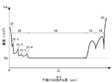
- the two or more low concentration peaks may be two or more concentration peaks arranged farthest from the lower surface of the semiconductor substrate among the concentration peaks.
- the active side gate wiring 131 is provided in the active portion 160. By providing the active side gate wiring 131 in the active portion 160, it is possible to reduce the variation in the wiring length from the gate pad 112 in each region of the semiconductor substrate 10.
- an N + type cathode region 82 is provided below the buffer region 20.
- the donor concentration in the cathode region 82 is higher than the donor concentration in the drift region 18.
- the donor of the cathode region 82 is, for example, hydrogen or phosphorus.
- the elements that serve as donors and acceptors in each region are not limited to the above-mentioned examples.
- the collector region 22 and the cathode region 82 are exposed on the lower surface 23 of the semiconductor substrate 10 and are connected to the collector electrode 24.
- the collector electrode 24 may come into contact with the entire lower surface 23 of the semiconductor substrate 10.
- the emitter electrode 52 and the collector electrode 24 are made of a metal material such as aluminum.
- a part of the buffer area 20 of this example is arranged on the upper surface 21 side of the semiconductor substrate 10.
- the plurality of concentration peaks 25 at least the deepest peak is arranged on the upper surface 21 side.
- the remaining concentration peak 25 is arranged on the lower surface 23 side of the semiconductor substrate 10 as in the example of FIG.
- the doping concentration at the center Zc in the depth direction of the semiconductor substrate 10 is defined as Dc.
- the central Zc is contained in the high concentration region 128.
- the doping concentration Dc is higher than the bulk doping concentration Db.
- the peak value of the doping concentration of the low concentration peak in this example may be 50 times or less, 20 times or less, 10 times or less, or 8 times or less of the doping concentration Dc. It may be 5 times or less, 3 times or less, or 2 times or less.
- the average value of the peak values of the doping concentrations of the concentration peaks 25-5 and the concentration peaks 25-4 may be 50 times or less, 20 times or less, and 10 times or less the doping concentration Dc. It may be 8 times or less, 5 times or less, 3 times or less, or 2 times or less.
Abstract
Provided is a semiconductor device comprising a first-electroconductivity-type drift region provided to a semiconductor substrate, and a first-electroconductivity-type buffer region provided between the drift region and the bottom surface of the semiconductor substrate, the buffer region having, in the depth direction of the semiconductor substrate, three or more density peaks for which the doping density is higher than the draft region, the three or more density peaks including: a shallowest peak that is nearest to the bottom surface of the semiconductor substrate; a high-density peak disposed in a position separated farther than the shallowest peak from the bottom surface of the semiconductor substrate; and a low-density peak disposed in a position farther separated than the high-density peak from the bottom surface of the semiconductor substrate, the doping density of the low-density peak being 1/5 or less the doping density of the high-density peak.
Description
本発明は、半導体装置に関する。
The present invention relates to a semiconductor device.
従来、IGBT(絶縁ゲート型バイポーラトランジスタ)等の半導体素子において、ドリフト領域の下方にN+型のバッファ領域を設ける構造が知られている(例えば特許文献1参照)。
特許文献1 WO2013/147275号 Conventionally, in a semiconductor element such as an IGBT (insulated gate type bipolar transistor), a structure in which an N + type buffer region is provided below the drift region is known (see, for example, Patent Document 1).
Patent Document 1 WO2013 / 147275
特許文献1 WO2013/147275号 Conventionally, in a semiconductor element such as an IGBT (insulated gate type bipolar transistor), a structure in which an N + type buffer region is provided below the drift region is known (see, for example, Patent Document 1).
バッファ領域における電界集中を緩和することが好ましい。
It is preferable to relax the electric field concentration in the buffer region.
上記課題を解決するために、本発明の一つの態様においては、半導体装置を提供する。半導体装置は、半導体基板に設けられた第1導電型のドリフト領域を備えてよい。半導体装置は、ドリフト領域と半導体基板の下面との間に設けられ、ドリフト領域よりもドーピング濃度が高い濃度ピークを、半導体基板の深さ方向に3つ以上有する第1導電型のバッファ領域を備えてよい。3つ以上の濃度ピークは、半導体基板の下面に最も近い最浅ピークを含んでよい。3つ以上の濃度ピークは、最浅ピークよりも半導体基板の下面から離れた位置に配置された高濃度ピークを含んでよい。3つ以上の濃度ピークは、高濃度ピークよりも半導体基板の下面から離れた位置に配置され、ドーピング濃度が高濃度ピークの1/5以下である1つ以上の低濃度ピークを含んでよい。
In order to solve the above problems, a semiconductor device is provided in one aspect of the present invention. The semiconductor device may include a first conductive type drift region provided on the semiconductor substrate. The semiconductor device is provided between the drift region and the lower surface of the semiconductor substrate, and includes a first conductive type buffer region having three or more concentration peaks having a doping concentration higher than that of the drift region in the depth direction of the semiconductor substrate. You can. The three or more concentration peaks may include the shallowest peak closest to the lower surface of the semiconductor substrate. The three or more concentration peaks may include a high concentration peak arranged at a position farther from the lower surface of the semiconductor substrate than the shallowest peak. The three or more concentration peaks may be arranged at a position farther from the lower surface of the semiconductor substrate than the high concentration peak, and may include one or more low concentration peaks having a doping concentration of 1/5 or less of the high concentration peak.
バッファ領域は、濃度ピークと対応する水素濃度ピークを有してよい。半導体装置は、バッファ領域と半導体基板の下面との間に設けられた、第2導電型のコレクタ領域を備えてよい。
The buffer region may have a hydrogen concentration peak corresponding to the concentration peak. The semiconductor device may include a second conductive collector region provided between the buffer region and the lower surface of the semiconductor substrate.
低濃度ピークは、濃度ピークのうち、半導体基板の下面から最も離れて配置された最深ピークであってよい。
The low concentration peak may be the deepest peak arranged farthest from the lower surface of the semiconductor substrate among the concentration peaks.
3つ以上の濃度ピークは、半導体基板の下面から最も離れて配置された最深ピークを含み、低濃度ピークは、高濃度ピークと、最深ピークとの間に配置されていてよい。
The three or more concentration peaks include the deepest peak arranged farthest from the lower surface of the semiconductor substrate, and the low concentration peak may be arranged between the high concentration peak and the deepest peak.
3つ以上の濃度ピークは、低濃度ピークを2つ以上含んでよい。
The concentration peak of 3 or more may include 2 or more low concentration peaks.
2つ以上の低濃度ピークは、濃度ピークのうち、半導体基板の下面から最も遠くに配置された2つ以上の濃度ピークであってよい。
The two or more low concentration peaks may be two or more concentration peaks arranged farthest from the lower surface of the semiconductor substrate among the concentration peaks.
低濃度ピークのドーピング濃度は、半導体基板のバルク・ドナー濃度の50倍以下であってよい。
The doping concentration of the low concentration peak may be 50 times or less of the bulk donor concentration of the semiconductor substrate.
低濃度ピークのドーピング濃度は、半導体基板の深さ方向の中央におけるドーピング濃度の50倍以下であってよい。
The doping concentration of the low concentration peak may be 50 times or less the doping concentration at the center in the depth direction of the semiconductor substrate.
3つ以上の濃度ピークは、半導体基板の下面から最も離れて配置された第1ピークと、深さ方向において第1ピークと隣り合う第2ピークとを含んでよい。第1ピークおよび第2ピークのドーピング濃度のピーク値の平均値は、高濃度ピークのドーピング濃度のピーク値の1/5以下であってよい。
The three or more concentration peaks may include a first peak arranged farthest from the lower surface of the semiconductor substrate and a second peak adjacent to the first peak in the depth direction. The average value of the peak values of the doping concentrations of the first peak and the second peak may be 1/5 or less of the peak value of the doping concentration of the high concentration peak.
第1ピークおよび第2ピークのドーピング濃度のピーク値の平均値は、半導体基板のバルク・ドナー濃度の50倍以下であってよい。
The average value of the peak values of the doping concentrations of the first peak and the second peak may be 50 times or less the bulk donor concentration of the semiconductor substrate.
第1ピークおよび第2ピークのドーピング濃度のピーク値の平均値は、半導体基板の深さ方向の中央におけるドーピング濃度の50倍以下であってよい。
The average value of the peak values of the doping concentrations of the first peak and the second peak may be 50 times or less of the doping concentration at the center in the depth direction of the semiconductor substrate.
バッファ領域は再結合中心を含んでよい。再結合中心の深さ方向における密度ピークが、最浅ピークと、高濃度ピークとの間に配置されていてよい。
The buffer area may include a recombination center. The density peak in the depth direction of the recombination center may be arranged between the shallowest peak and the high concentration peak.
密度ピークが、最浅ピークと高濃度ピークとの間において最浅ピークよりに配置されていてよい。
The density peak may be arranged more than the shallowest peak between the shallowest peak and the high concentration peak.
濃度ピークのうち、半導体基板の下面から最も離れて配置された最深ピークのドーピング濃度は、最深ピークと深さ方向において隣り合う濃度ピークのドーピング濃度の1.1倍以上、5倍以下であってよい。
Among the concentration peaks, the doping concentration of the deepest peak arranged farthest from the lower surface of the semiconductor substrate is 1.1 times or more and 5 times or less of the doping concentration of the concentration peaks adjacent to the deepest peak in the depth direction. Good.
濃度ピークのうち、半導体基板の下面から最も離れて配置された最深ピークのドーピング濃度は、1.0×10¹⁴atoms/cm3以上、5.0×1014atoms/cm3以下であってよい。
Among the concentration peaks, the doping concentration of the deepest peak arranged farthest from the lower surface of the semiconductor substrate may be 1.0 × 10 14 atoms / cm 3 or more and 5.0 × 10 14 atoms / cm 3 or less. ..
バッファ領域は、半導体基板の下面と、半導体基板の深さ方向の中央との間に配置されていてよい。
The buffer area may be arranged between the lower surface of the semiconductor substrate and the center in the depth direction of the semiconductor substrate.
濃度ピークのうち、半導体基板の下面から最も離れて配置された最深ピークは、半導体基板の上面と、半導体基板の深さ方向の中央との間に配置されていてよい。
Of the concentration peaks, the deepest peak arranged farthest from the lower surface of the semiconductor substrate may be arranged between the upper surface of the semiconductor substrate and the center in the depth direction of the semiconductor substrate.
なお、上記の発明の概要は、本発明の必要な特徴の全てを列挙したものではない。また、これらの特徴群のサブコンビネーションもまた、発明となりうる。
The outline of the above invention does not list all the necessary features of the present invention. Sub-combinations of these feature groups can also be inventions.
以下、発明の実施の形態を通じて本発明を説明するが、以下の実施形態は請求の範囲にかかる発明を限定するものではない。また、実施形態の中で説明されている特徴の組み合わせの全てが発明の解決手段に必須であるとは限らない。
Hereinafter, the present invention will be described through embodiments of the invention, but the following embodiments do not limit the inventions claimed. Also, not all combinations of features described in the embodiments are essential to the means of solving the invention.
本明細書においては半導体基板の深さ方向と平行な方向における一方の側を「上」、他方の側を「下」と称する。基板、層またはその他の部材の2つの主面のうち、一方の面を上面、他方の面を下面と称する。「上」、「下」の方向は、重力方向または半導体装置の実装時における方向に限定されない。
In this specification, one side in the direction parallel to the depth direction of the semiconductor substrate is referred to as "upper" and the other side is referred to as "lower". Of the two main surfaces of the substrate, layer or other member, one surface is referred to as the upper surface and the other surface is referred to as the lower surface. The "up" and "down" directions are not limited to the direction of gravity or the direction when the semiconductor device is mounted.
本明細書では、X軸、Y軸およびZ軸の直交座標軸を用いて技術的事項を説明する場合がある。直交座標軸は、構成要素の相対位置を特定するに過ぎず、特定の方向を限定するものではない。例えば、Z軸は地面に対する高さ方向を限定して示すものではない。なお、+Z軸方向と-Z軸方向とは互いに逆向きの方向である。正負を記載せず、Z軸方向と記載した場合、+Z軸および-Z軸に平行な方向を意味する。
In this specification, technical matters may be described using Cartesian coordinate axes of the X-axis, the Y-axis, and the Z-axis. The orthogonal coordinate axes only specify the relative positions of the components and do not limit the specific direction. For example, the Z axis does not limit the height direction with respect to the ground. The + Z-axis direction and the −Z-axis direction are opposite to each other. When the positive and negative directions are not described and the Z-axis direction is described, it means the direction parallel to the + Z-axis and the -Z-axis.
本明細書では、半導体基板の上面および下面に平行な直交軸をX軸およびY軸とする。また、半導体基板の上面および下面と垂直な軸をZ軸とする。本明細書では、Z軸の方向を深さ方向と称する場合がある。また、本明細書では、X軸およびY軸を含めて、半導体基板の上面および下面に平行な方向を、水平方向と称する場合がある。
In the present specification, the orthogonal axes parallel to the upper surface and the lower surface of the semiconductor substrate are defined as the X axis and the Y axis. Further, the axis perpendicular to the upper surface and the lower surface of the semiconductor substrate is defined as the Z axis. In the present specification, the direction of the Z axis may be referred to as a depth direction. Further, in the present specification, the direction parallel to the upper surface and the lower surface of the semiconductor substrate including the X-axis and the Y-axis may be referred to as a horizontal direction.
本明細書において「同一」または「等しい」のように称した場合、製造ばらつき等に起因する誤差を有する場合も含んでよい。当該誤差は、例えば10%以内である。
When referred to as "same" or "equal" in the present specification, it may include a case where there is an error due to manufacturing variation or the like. The error is, for example, within 10%.
本明細書においては、不純物がドーピングされたドーピング領域の導電型をP型またはN型として説明している。本明細書においては、不純物とは、特にN型のドナーまたはP型のアクセプタのいずれかを意味する場合があり、ドーパントと記載する場合がある。本明細書においては、ドーピングとは、半導体基板にドナーまたはアクセプタを導入し、N型の導電型を示す半導体またはP型の導電型を示す半導体とすることを意味する。
In this specification, the conductive type of the doping region in which impurities are doped is described as P type or N type. As used herein, an impurity may mean either an N-type donor or a P-type acceptor in particular, and may be referred to as a dopant. As used herein, doping means that a donor or acceptor is introduced into a semiconductor substrate to obtain a semiconductor exhibiting an N-type conductive type or a semiconductor exhibiting a P-type conductive type.
本明細書においては、ドーピング濃度とは、熱平衡状態におけるドナーの濃度またはアクセプタの濃度を意味する。本明細書においては、ネット・ドーピング濃度とは、ドナー濃度を正イオンの濃度とし、アクセプタ濃度を負イオンの濃度として、電荷の極性を含めて足し合わせた正味の濃度を意味する。一例として、ドナー濃度をND、アクセプタ濃度をNAとすると、任意の位置における正味のネット・ドーピング濃度はND-NAとなる。本明細書では、ネット・ドーピング濃度を単にドーピング濃度と記載する場合がある。
As used herein, the doping concentration means the concentration of a donor or the concentration of an acceptor in a thermal equilibrium state. As used herein, the net doping concentration means the net concentration of the donor concentration as the concentration of positive ions and the acceptor concentration as the concentration of negative ions, including the polarity of the charge. As an example, the donor concentration N D, the acceptor concentration and N A, the net doping concentration of the net at any position is N D -N A. In the present specification, the net doping concentration may be simply referred to as a doping concentration.
ドナーは、半導体に電子を供給する機能を有している。アクセプタは、半導体から電子を受け取る機能を有している。ドナーおよびアクセプタは、不純物自体には限定されない。例えば、半導体中に存在する空孔(V)、酸素(O)および水素(H)が結合したVOH欠陥は、電子を供給するドナーとして機能する。本明細書では、VOH欠陥を水素ドナーと称する場合がある。
The donor has the function of supplying electrons to the semiconductor. The acceptor has a function of receiving electrons from a semiconductor. Donors and acceptors are not limited to the impurities themselves. For example, a VOH defect in which pores (V), oxygen (O) and hydrogen (H) are bonded in a semiconductor functions as a donor that supplies electrons. VOH defects are sometimes referred to herein as hydrogen donors.
本明細書においてP+型またはN+型と記載した場合、P型またはN型よりもドーピング濃度が高いことを意味し、P-型またはN-型と記載した場合、P型またはN型よりもドーピング濃度が低いことを意味する。また、本明細書においてP++型またはN++型と記載した場合には、P+型またはN+型よりもドーピング濃度が高いことを意味する。
In the present specification, the description of P + type or N + type means that the doping concentration is higher than that of P type or N type, and the description of P-type or N-type means that the doping concentration is higher than that of P type or N type. It means that the concentration is low. Moreover, when it is described as P ++ type or N ++ type in this specification, it means that the doping concentration is higher than that of P + type or N + type.
本明細書において化学濃度とは、電気的な活性化の状態によらずに測定される不純物の濃度を指す。化学濃度は、例えば二次イオン質量分析法(SIMS)により計測できる。上述したネット・ドーピング濃度は、電圧-容量測定法(CV法)により測定できる。また、拡がり抵抗測定法(SR法)により計測されるキャリア濃度を、ネット・ドーピング濃度としてよい。CV法またはSR法により計測されるキャリア濃度は、熱平衡状態における値としてよい。また、N型の領域においては、ドナー濃度がアクセプタ濃度よりも十分大きいので、当該領域におけるキャリア濃度を、ドナー濃度としてもよい。同様に、P型の領域においては、当該領域におけるキャリア濃度を、アクセプタ濃度としてもよい。本明細書では、N型領域のドーピング濃度をドナー濃度と称する場合があり、P型領域のドーピング濃度をアクセプタ濃度と称する場合がある。
In the present specification, the chemical concentration refers to the concentration of impurities measured regardless of the state of electrical activation. The chemical concentration can be measured, for example, by secondary ion mass spectrometry (SIMS). The net doping concentration described above can be measured by a voltage-capacity measurement method (CV method). Further, the carrier concentration measured by the spread resistance measurement method (SR method) may be used as the net doping concentration. The carrier concentration measured by the CV method or the SR method may be a value in a thermal equilibrium state. Moreover, since the donor concentration is sufficiently higher than the acceptor concentration in the N-type region, the carrier concentration in the region may be used as the donor concentration. Similarly, in the P-type region, the carrier concentration in the region may be used as the acceptor concentration. In the present specification, the doping concentration in the N-type region may be referred to as the donor concentration, and the doping concentration in the P-type region may be referred to as the acceptor concentration.
また、ドナー、アクセプタまたはネット・ドーピングの濃度分布がピークを有する場合、当該ピーク値を当該領域におけるドナー、アクセプタまたはネット・ドーピングの濃度としてよい。ドナー、アクセプタまたはネット・ドーピングの濃度がほぼ均一な場合等においては、当該領域におけるドナー、アクセプタまたはネット・ドーピングの濃度の平均値をドナー、アクセプタまたはネット・ドーピングの濃度としてよい。
If the concentration distribution of donor, acceptor or net doping has a peak, the peak value may be used as the concentration of donor, acceptor or net doping in the region. When the concentration of donor, acceptor or net doping is substantially uniform, the average value of the concentration of donor, acceptor or net doping in the region may be used as the concentration of donor, acceptor or net doping.
SR法により計測されるキャリア濃度が、ドナーまたはアクセプタの濃度より低くてもよい。拡がり抵抗を測定する際に電流が流れる範囲において、半導体基板のキャリア移動度が結晶状態の値よりも低い場合がある。キャリア移動度の低下は、格子欠陥等による結晶構造の乱れ(ディスオーダー)により、キャリアが散乱されることで生じる。
The carrier concentration measured by the SR method may be lower than the concentration of the donor or acceptor. In the range in which a current flows when measuring the spread resistance, the carrier mobility of the semiconductor substrate may be lower than the value in the crystalline state. The decrease in carrier mobility occurs when carriers are scattered due to disorder (disorder) of the crystal structure due to lattice defects or the like.
CV法またはSR法により計測されるキャリア濃度から算出したドナーまたはアクセプタの濃度は、ドナーまたはアクセプタを示す元素の化学濃度よりも低くてよい。一例として、シリコンの半導体においてドナーとなるリンまたはヒ素のドナー濃度、あるいはアクセプタとなるボロン(ホウ素)のアクセプタ濃度は、これらの化学濃度の99%程度である。一方、シリコンの半導体においてドナーとなる水素のドナー濃度は、水素の化学濃度の0.1%から10%程度である。本明細書の単位系は、特に断りがなければSI単位系である。長さの単位をcm等で表示することがあるが、諸計算はメートル(m)に換算してから行ってよい。
The concentration of the donor or acceptor calculated from the carrier concentration measured by the CV method or the SR method may be lower than the chemical concentration of the element indicating the donor or acceptor. As an example, the donor concentration of phosphorus or arsenic as a donor in a silicon semiconductor, or the acceptor concentration of boron (boron) as an acceptor is about 99% of these chemical concentrations. On the other hand, the donor concentration of hydrogen as a donor in a silicon semiconductor is about 0.1% to 10% of the chemical concentration of hydrogen. Unless otherwise specified, the unit system of the present specification is the SI unit system. The unit of length may be displayed in cm or the like, but various calculations may be performed after converting to meters (m).
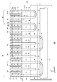
図1は、本発明の一つの実施形態に係る半導体装置100の一例を示す上面図である。図1においては、各部材を半導体基板10の上面に投影した位置を示している。図1においては、半導体装置100の一部の部材だけを示しており、一部の部材は省略している。
FIG. 1 is a top view showing an example of a semiconductor device 100 according to an embodiment of the present invention. FIG. 1 shows a position where each member is projected onto the upper surface of the semiconductor substrate 10. In FIG. 1, only a part of the members of the semiconductor device 100 is shown, and some members are omitted.
半導体装置100は、半導体基板10を備えている。半導体基板10は、上面視において端辺102を有する。本明細書で単に上面視と称した場合、半導体基板10の上面側から見ることを意味している。本例の半導体基板10は、上面視において互いに向かい合う2組の端辺102を有する。図1においては、X軸およびY軸は、いずれかの端辺102と平行である。またZ軸は、半導体基板10の上面と垂直である。
The semiconductor device 100 includes a semiconductor substrate 10. The semiconductor substrate 10 has an end side 102 when viewed from above. When simply referred to as a top view in the present specification, it means that the semiconductor substrate 10 is viewed from the top surface side. The semiconductor substrate 10 of this example has two sets of end sides 102 facing each other in a top view. In FIG. 1, the X-axis and the Y-axis are parallel to either end 102. The Z axis is perpendicular to the upper surface of the semiconductor substrate 10.
半導体基板10には活性部160が設けられている。活性部160は、半導体装置100が動作した場合に半導体基板10の上面と下面との間で、深さ方向に主電流が流れる領域である。活性部160の上方には、エミッタ電極が設けられているが図1では省略している。
The semiconductor substrate 10 is provided with an active portion 160. The active portion 160 is a region in which a main current flows in the depth direction between the upper surface and the lower surface of the semiconductor substrate 10 when the semiconductor device 100 operates. An emitter electrode is provided above the active portion 160, but is omitted in FIG.
活性部160には、IGBT等のトランジスタ素子を含むトランジスタ部70と、還流ダイオード(FWD)等のダイオード素子を含むダイオード部80の少なくとも一方が設けられている。図1の例では、トランジスタ部70およびダイオード部80は、半導体基板10の上面における所定の配列方向(本例ではX軸方向)に沿って、交互に配置されている。他の例では、活性部160には、トランジスタ部70およびダイオード部80の一方だけが設けられていてもよい。
The active unit 160 is provided with at least one of a transistor unit 70 including a transistor element such as an IGBT and a diode unit 80 including a diode element such as a freewheeling diode (FWD). In the example of FIG. 1, the transistor portion 70 and the diode portion 80 are alternately arranged along a predetermined arrangement direction (X-axis direction in this example) on the upper surface of the semiconductor substrate 10. In another example, the active portion 160 may be provided with only one of the transistor portion 70 and the diode portion 80.
図1においては、トランジスタ部70が配置される領域には記号「I」を付し、ダイオード部80が配置される領域には記号「F」を付している。本明細書では、上面視において配列方向と垂直な方向を延伸方向(図1ではY軸方向)と称する場合がある。トランジスタ部70およびダイオード部80は、それぞれ延伸方向に長手を有してよい。つまり、トランジスタ部70のY軸方向における長さは、X軸方向における幅よりも大きい。同様に、ダイオード部80のY軸方向における長さは、X軸方向における幅よりも大きい。トランジスタ部70およびダイオード部80の延伸方向と、後述する各トレンチ部の長手方向とは同一であってよい。
In FIG. 1, the symbol "I" is attached to the region where the transistor portion 70 is arranged, and the symbol "F" is attached to the region where the diode portion 80 is arranged. In the present specification, the direction perpendicular to the arrangement direction in the top view may be referred to as a stretching direction (Y-axis direction in FIG. 1). The transistor portion 70 and the diode portion 80 may each have a longitudinal length in the stretching direction. That is, the length of the transistor portion 70 in the Y-axis direction is larger than the width in the X-axis direction. Similarly, the length of the diode portion 80 in the Y-axis direction is larger than the width in the X-axis direction. The stretching direction of the transistor portion 70 and the diode portion 80 may be the same as the longitudinal direction of each trench portion described later.
ダイオード部80は、半導体基板10の下面と接する領域に、N+型のカソード領域を有する。本明細書では、カソード領域が設けられた領域を、ダイオード部80と称する。つまりダイオード部80は、上面視においてカソード領域と重なる領域である。半導体基板10の下面のカソード領域以外の領域には、P+型のコレクタ領域が設けられてよい。本明細書では、ダイオード部80を、後述するゲート配線までY軸方向に延長した延長領域81も、ダイオード部80に含める場合がある。延長領域81の下面には、コレクタ領域が設けられている。
The diode portion 80 has an N + type cathode region in a region in contact with the lower surface of the semiconductor substrate 10. In the present specification, the region provided with the cathode region is referred to as a diode portion 80. That is, the diode portion 80 is a region that overlaps with the cathode region in the top view. A P + type collector region may be provided in a region other than the cathode region on the lower surface of the semiconductor substrate 10. In the present specification, the diode portion 80 may also include an extension region 81 in which the diode portion 80 is extended in the Y-axis direction to the gate wiring described later. A collector region is provided on the lower surface of the extension region 81.
トランジスタ部70は、半導体基板10の下面と接する領域に、P+型のコレクタ領域を有する。また、トランジスタ部70は、半導体基板10の上面側にゲート構造が周期的に配置されている。ゲート構造は、N型のエミッタ領域、P型のベース領域、ゲート導電部およびゲート絶縁膜を有する。
The transistor portion 70 has a P + type collector region in a region in contact with the lower surface of the semiconductor substrate 10. Further, in the transistor portion 70, a gate structure is periodically arranged on the upper surface side of the semiconductor substrate 10. The gate structure has an N-type emitter region, a P-type base region, a gate conductive portion, and a gate insulating film.
半導体装置100は、半導体基板10の上方に1つ以上のパッドを有してよい。本例の半導体装置100は、ゲートパッド112を有している。半導体装置100は、アノードパッド、カソードパッドおよび電流検出パッド等のパッドを有してもよい。各パッドは、端辺102の近傍に配置されている。端辺102の近傍とは、上面視における端辺102と、エミッタ電極との間の領域を指す。半導体装置100の実装時において、各パッドは、ワイヤ等の配線を介して外部の回路に接続されてよい。
The semiconductor device 100 may have one or more pads above the semiconductor substrate 10. The semiconductor device 100 of this example has a gate pad 112. The semiconductor device 100 may have pads such as an anode pad, a cathode pad, and a current detection pad. Each pad is arranged in the vicinity of the end side 102. The vicinity of the end side 102 refers to a region between the end side 102 and the emitter electrode in top view. At the time of mounting the semiconductor device 100, each pad may be connected to an external circuit via wiring such as a wire.
ゲートパッド112には、ゲート電位が印加される。ゲートパッド112は、活性部160のゲートトレンチ部の導電部に電気的に接続される。半導体装置100は、ゲートパッド112とゲートトレンチ部とを接続するゲート配線を備える。図1においては、ゲート配線に斜線のハッチングを付している。
A gate potential is applied to the gate pad 112. The gate pad 112 is electrically connected to the conductive portion of the gate trench portion of the active portion 160. The semiconductor device 100 includes a gate wiring that connects the gate pad 112 and the gate trench portion. In FIG. 1, diagonal hatching is attached to the gate wiring.
本例のゲート配線は、外周ゲート配線130と、活性側ゲート配線131とを有している。外周ゲート配線130は、上面視において活性部160と半導体基板10の端辺102との間に配置されている。本例の外周ゲート配線130は、上面視において活性部160を囲んでいる。上面視において外周ゲート配線130に囲まれた領域を活性部160としてもよい。また、外周ゲート配線130は、ゲートパッド112と接続されている。外周ゲート配線130は、半導体基板10の上方に配置されている。外周ゲート配線130は、アルミニウム等を含む金属配線であってよい。
The gate wiring of this example has an outer peripheral gate wiring 130 and an active side gate wiring 131. The outer peripheral gate wiring 130 is arranged between the active portion 160 and the end side 102 of the semiconductor substrate 10 in a top view. The outer peripheral gate wiring 130 of this example surrounds the active portion 160 in a top view. The region surrounded by the outer peripheral gate wiring 130 in the top view may be the active portion 160. Further, the outer peripheral gate wiring 130 is connected to the gate pad 112. The outer peripheral gate wiring 130 is arranged above the semiconductor substrate 10. The outer peripheral gate wiring 130 may be a metal wiring containing aluminum or the like.
活性側ゲート配線131は、活性部160に設けられている。活性部160に活性側ゲート配線131を設けることで、半導体基板10の各領域について、ゲートパッド112からの配線長のバラツキを低減できる。
The active side gate wiring 131 is provided in the active portion 160. By providing the active side gate wiring 131 in the active portion 160, it is possible to reduce the variation in the wiring length from the gate pad 112 in each region of the semiconductor substrate 10.
活性側ゲート配線131は、活性部160のゲートトレンチ部と接続される。活性側ゲート配線131は、半導体基板10の上方に配置されている。活性側ゲート配線131は、不純物がドープされたポリシリコン等の半導体で形成された配線であってよい。
The active side gate wiring 131 is connected to the gate trench portion of the active portion 160. The active side gate wiring 131 is arranged above the semiconductor substrate 10. The active side gate wiring 131 may be wiring formed of a semiconductor such as polysilicon doped with impurities.
活性側ゲート配線131は、外周ゲート配線130と接続されてよい。本例の活性側ゲート配線131は、一方の外周ゲート配線130から他方の外周ゲート配線130まで、Y軸方向の略中央で活性部160を横切るように、X軸方向に延伸して設けられている。活性側ゲート配線131により活性部160が分割されている場合、それぞれの分割領域において、トランジスタ部70およびダイオード部80がX軸方向に交互に配置されてよい。
The active side gate wiring 131 may be connected to the outer peripheral gate wiring 130. The active side gate wiring 131 of this example is provided extending from one outer peripheral gate wiring 130 to the other outer peripheral gate wiring 130 in the X-axis direction so as to cross the active portion 160 at substantially the center in the Y-axis direction. There is. When the active portion 160 is divided by the active side gate wiring 131, the transistor portion 70 and the diode portion 80 may be alternately arranged in the X-axis direction in each divided region.
また、半導体装置100は、ポリシリコン等で形成されたPN接合ダイオードである不図示の温度センス部や、活性部160に設けられたトランジスタ部の動作を模擬する不図示の電流検出部を備えてもよい。
Further, the semiconductor device 100 includes a temperature sense unit (not shown) which is a PN junction diode made of polysilicon or the like, and a current detection unit (not shown) which simulates the operation of a transistor unit provided in the active unit 160. May be good.
本例の半導体装置100は、活性部160と端辺102との間に、エッジ終端構造部90を備える。本例のエッジ終端構造部90は、外周ゲート配線130と端辺102との間に配置されている。エッジ終端構造部90は、半導体基板10の上面側の電界集中を緩和する。エッジ終端構造部90は、活性部160を囲んで環状に設けられたガードリング、フィールドプレートおよびリサーフのうちの少なくとも一つを更に備えていてもよい。
The semiconductor device 100 of this example includes an edge termination structure portion 90 between the active portion 160 and the end side 102. The edge termination structure 90 of this example is arranged between the outer peripheral gate wiring 130 and the end side 102. The edge termination structure 90 relaxes the electric field concentration on the upper surface side of the semiconductor substrate 10. The edge termination structure 90 may further include at least one of a guard ring, a field plate and a resurf provided in an annular shape surrounding the active portion 160.
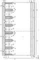
図2は、図1における領域Aの拡大図である。領域Aは、トランジスタ部70、ダイオード部80、および、活性側ゲート配線131を含む領域である。本例の半導体装置100は、半導体基板10の上面側の内部に設けられたゲートトレンチ部40、ダミートレンチ部30、ウェル領域11、エミッタ領域12、ベース領域14およびコンタクト領域15を備える。ゲートトレンチ部40およびダミートレンチ部30は、それぞれがトレンチ部の一例である。また、本例の半導体装置100は、半導体基板10の上面の上方に設けられたエミッタ電極52および活性側ゲート配線131を備える。エミッタ電極52および活性側ゲート配線131は互いに分離して設けられる。
FIG. 2 is an enlarged view of the area A in FIG. The region A is a region including the transistor portion 70, the diode portion 80, and the active side gate wiring 131. The semiconductor device 100 of this example includes a gate trench portion 40, a dummy trench portion 30, a well region 11, an emitter region 12, a base region 14, and a contact region 15 provided inside the upper surface side of the semiconductor substrate 10. The gate trench portion 40 and the dummy trench portion 30 are examples of trench portions, respectively. Further, the semiconductor device 100 of this example includes an emitter electrode 52 and an active side gate wiring 131 provided above the upper surface of the semiconductor substrate 10. The emitter electrode 52 and the active side gate wiring 131 are provided separately from each other.
エミッタ電極52および活性側ゲート配線131と、半導体基板10の上面との間には層間絶縁膜が設けられるが、図1では省略している。本例の層間絶縁膜には、コンタクトホール54が、当該層間絶縁膜を貫通して設けられる。図2においては、それぞれのコンタクトホール54に斜線のハッチングを付している。
An interlayer insulating film is provided between the emitter electrode 52 and the active side gate wiring 131 and the upper surface of the semiconductor substrate 10, but this is omitted in FIG. In the interlayer insulating film of this example, a contact hole 54 is provided so as to penetrate the interlayer insulating film. In FIG. 2, each contact hole 54 is hatched with diagonal lines.
エミッタ電極52は、ゲートトレンチ部40、ダミートレンチ部30、ウェル領域11、エミッタ領域12、ベース領域14およびコンタクト領域15の上方に設けられる。エミッタ電極52は、コンタクトホール54を通って、半導体基板10の上面におけるエミッタ領域12、コンタクト領域15およびベース領域14と接触する。また、エミッタ電極52は、層間絶縁膜に設けられたコンタクトホールを通って、ダミートレンチ部30内のダミー導電部と接続される。エミッタ電極52は、Y軸方向におけるダミートレンチ部30の先端において、ダミートレンチ部30のダミー導電部と接続されてよい。
The emitter electrode 52 is provided above the gate trench portion 40, the dummy trench portion 30, the well region 11, the emitter region 12, the base region 14, and the contact region 15. The emitter electrode 52 passes through the contact hole 54 and comes into contact with the emitter region 12, the contact region 15, and the base region 14 on the upper surface of the semiconductor substrate 10. Further, the emitter electrode 52 is connected to the dummy conductive portion in the dummy trench portion 30 through a contact hole provided in the interlayer insulating film. The emitter electrode 52 may be connected to the dummy conductive portion of the dummy trench portion 30 at the tip of the dummy trench portion 30 in the Y-axis direction.
活性側ゲート配線131は、層間絶縁膜に設けられたコンタクトホールを通って、ゲートトレンチ部40と接続する。活性側ゲート配線131は、Y軸方向におけるゲートトレンチ部40の先端部41において、ゲートトレンチ部40のゲート導電部と接続されてよい。活性側ゲート配線131は、ダミートレンチ部30内のダミー導電部とは接続されない。
The active side gate wiring 131 is connected to the gate trench portion 40 through a contact hole provided in the interlayer insulating film. The active side gate wiring 131 may be connected to the gate conductive portion of the gate trench portion 40 at the tip portion 41 of the gate trench portion 40 in the Y-axis direction. The active side gate wiring 131 is not connected to the dummy conductive portion in the dummy trench portion 30.
エミッタ電極52は、金属を含む材料で形成される。図2においては、エミッタ電極52が設けられる範囲を示している。例えば、エミッタ電極52の少なくとも一部の領域はアルミニウム等の金属、または、アルミニウム等を含む金属合金で形成される。金属合金は、例えばアルミニウム‐シリコン合金、アルミニウム-シリコン-銅合金である。エミッタ電極52は、アルミニウム等で形成された領域の下層に、チタンやチタン化合物等で形成されたバリアメタルを有してよい。さらにコンタクトホール内において、タングステン等を埋め込んで形成されたプラグを有してもよい。プラグは、バリアメタルとアルミニウム等に接するように設けられる。
The emitter electrode 52 is made of a material containing metal. FIG. 2 shows a range in which the emitter electrode 52 is provided. For example, at least a part of the emitter electrode 52 is formed of a metal such as aluminum or a metal alloy containing aluminum or the like. The metal alloy is, for example, an aluminum-silicon alloy or an aluminum-silicon-copper alloy. The emitter electrode 52 may have a barrier metal formed of titanium, a titanium compound, or the like in the lower layer of the region formed of aluminum or the like. Further, a plug formed by embedding tungsten or the like may be provided in the contact hole. The plug is provided so as to be in contact with the barrier metal and aluminum or the like.
ウェル領域11は、活性側ゲート配線131と重なって設けられている。ウェル領域11は、活性側ゲート配線131と重ならない範囲にも、所定の幅で延伸して設けられている。本例のウェル領域11は、コンタクトホール54のY軸方向の端から、活性側ゲート配線131側に離れて設けられている。ウェル領域11は、ベース領域14よりもドーピング濃度の高い第2導電型の領域である。本例のベース領域14はP-型であり、ウェル領域11はP+型である。
The well region 11 is provided so as to overlap the active side gate wiring 131. The well region 11 is also extended to a predetermined width so as not to overlap with the active side gate wiring 131. The well region 11 of this example is provided away from the end of the contact hole 54 in the Y-axis direction on the active side gate wiring 131 side. The well region 11 is a second conductive type region having a higher doping concentration than the base region 14. The base region 14 of this example is P-type, and the well region 11 is P + type.
トランジスタ部70およびダイオード部80のそれぞれは、配列方向に複数配列されたトレンチ部を有する。本例のトランジスタ部70には、配列方向に沿って1つ以上のゲートトレンチ部40と、1つ以上のダミートレンチ部30とが交互に設けられている。本例のダイオード部80には、複数のダミートレンチ部30が、配列方向に沿って設けられている。本例のダイオード部80には、ゲートトレンチ部40が設けられていない。
Each of the transistor portion 70 and the diode portion 80 has a plurality of trench portions arranged in the arrangement direction. The transistor portion 70 of this example is provided with one or more gate trench portions 40 and one or more dummy trench portions 30 alternately along the arrangement direction. The diode portion 80 of this example is provided with a plurality of dummy trench portions 30 along the arrangement direction. The diode portion 80 of this example is not provided with the gate trench portion 40.
本例のゲートトレンチ部40は、配列方向と垂直な延伸方向に沿って延伸する2つの直線部分39(延伸方向に沿って直線状であるトレンチの部分)と、2つの直線部分39を接続する先端部41を有してよい。図2における延伸方向はY軸方向である。
The gate trench portion 40 of this example connects two straight portions 39 (a portion of the trench that is linear along the stretching direction) and two straight portions 39 that extend along the stretching direction perpendicular to the arrangement direction. It may have a tip 41. The stretching direction in FIG. 2 is the Y-axis direction.
先端部41の少なくとも一部は、上面視において曲線状に設けられることが好ましい。2つの直線部分39のY軸方向における端部どうしを先端部41が接続することで、直線部分39の端部における電界集中を緩和できる。
It is preferable that at least a part of the tip portion 41 is provided in a curved shape in a top view. By connecting the ends of the two straight portions 39 in the Y-axis direction to each other by the tip portion 41, the electric field concentration at the ends of the straight portions 39 can be relaxed.
トランジスタ部70において、ダミートレンチ部30はゲートトレンチ部40のそれぞれの直線部分39の間に設けられる。それぞれの直線部分39の間には、1本のダミートレンチ部30が設けられてよく、複数本のダミートレンチ部30が設けられていてもよい。ダミートレンチ部30は、延伸方向に延伸する直線形状を有してよく、ゲートトレンチ部40と同様に、直線部分29と先端部31とを有していてもよい。図2に示した半導体装置100は、先端部31を有さない直線形状のダミートレンチ部30と、先端部31を有するダミートレンチ部30の両方を含んでいる。
In the transistor portion 70, the dummy trench portion 30 is provided between the straight portions 39 of the gate trench portion 40. One dummy trench portion 30 may be provided between the straight portions 39, and a plurality of dummy trench portions 30 may be provided. The dummy trench portion 30 may have a linear shape extending in the stretching direction, and may have a straight portion 29 and a tip portion 31 as in the gate trench portion 40. The semiconductor device 100 shown in FIG. 2 includes both a linear dummy trench portion 30 having no tip portion 31 and a dummy trench portion 30 having a tip portion 31.
ウェル領域11の拡散深さは、ゲートトレンチ部40およびダミートレンチ部30の深さよりも深くてよい。ゲートトレンチ部40およびダミートレンチ部30のY軸方向の端部は、上面視においてウェル領域11に設けられる。つまり、各トレンチ部のY軸方向の端部において、各トレンチ部の深さ方向の底部は、ウェル領域11に覆われている。これにより、各トレンチ部の当該底部における電界集中を緩和できる。
The diffusion depth of the well region 11 may be deeper than the depth of the gate trench portion 40 and the dummy trench portion 30. The ends of the gate trench portion 40 and the dummy trench portion 30 in the Y-axis direction are provided in the well region 11 in the top view. That is, at the end of each trench in the Y-axis direction, the bottom of each trench in the depth direction is covered with the well region 11. As a result, the electric field concentration at the bottom of each trench can be relaxed.
配列方向において各トレンチ部の間には、メサ部が設けられている。メサ部は、半導体基板10の内部において、トレンチ部に挟まれた領域を指す。一例としてメサ部の上端は半導体基板10の上面である。メサ部の下端の深さ位置は、トレンチ部の下端の深さ位置と同一である。本例のメサ部は、半導体基板10の上面において、トレンチ部に沿って延伸方向(Y軸方向)に延伸して設けられている。本例では、トランジスタ部70にはメサ部60が設けられ、ダイオード部80にはメサ部61が設けられている。本明細書において単にメサ部と称した場合、メサ部60およびメサ部61のそれぞれを指している。
A mesa part is provided between each trench part in the arrangement direction. The mesa portion refers to a region sandwiched between trench portions inside the semiconductor substrate 10. As an example, the upper end of the mesa portion is the upper surface of the semiconductor substrate 10. The depth position of the lower end of the mesa portion is the same as the depth position of the lower end of the trench portion. The mesa portion of this example is provided on the upper surface of the semiconductor substrate 10 by extending in the stretching direction (Y-axis direction) along the trench portion. In this example, the transistor portion 70 is provided with a mesa portion 60, and the diode portion 80 is provided with a mesa portion 61. When simply referred to as a mesa portion in the present specification, it refers to each of the mesa portion 60 and the mesa portion 61.
それぞれのメサ部には、ベース領域14が設けられる。メサ部において半導体基板10の上面に露出したベース領域14のうち、活性側ゲート配線131に最も近く配置された領域をベース領域14-eとする。図2においては、それぞれのメサ部の延伸方向における一方の端部に配置されたベース領域14-eを示しているが、それぞれのメサ部の他方の端部にもベース領域14-eが配置されている。それぞれのメサ部には、上面視においてベース領域14-eに挟まれた領域に、第1導電型のエミッタ領域12および第2導電型のコンタクト領域15の少なくとも一方が設けられてよい。本例のエミッタ領域12はN+型であり、コンタクト領域15はP+型である。エミッタ領域12およびコンタクト領域15は、深さ方向において、ベース領域14と半導体基板10の上面との間に設けられてよい。
A base region 14 is provided in each mesa section. Of the base region 14 exposed on the upper surface of the semiconductor substrate 10 in the mesa portion, the region closest to the active side gate wiring 131 is referred to as the base region 14-e. In FIG. 2, the base region 14-e arranged at one end in the extending direction of each mesa portion is shown, but the base region 14-e is also arranged at the other end of each mesa portion. Has been done. At least one of the first conductive type emitter region 12 and the second conductive type contact region 15 may be provided in each mesa portion in the region sandwiched between the base regions 14-e in the top view. The emitter region 12 of this example is N + type, and the contact region 15 is P + type. The emitter region 12 and the contact region 15 may be provided between the base region 14 and the upper surface of the semiconductor substrate 10 in the depth direction.
トランジスタ部70のメサ部60は、半導体基板10の上面に露出したエミッタ領域12を有する。エミッタ領域12は、ゲートトレンチ部40に接して設けられている。ゲートトレンチ部40に接するメサ部60は、半導体基板10の上面に露出したコンタクト領域15が設けられていてよい。
The mesa portion 60 of the transistor portion 70 has an emitter region 12 exposed on the upper surface of the semiconductor substrate 10. The emitter region 12 is provided in contact with the gate trench portion 40. The mesa portion 60 in contact with the gate trench portion 40 may be provided with an exposed contact region 15 on the upper surface of the semiconductor substrate 10.
メサ部60におけるコンタクト領域15およびエミッタ領域12のそれぞれは、X軸方向における一方のトレンチ部から、他方のトレンチ部まで設けられる。一例として、メサ部60のコンタクト領域15およびエミッタ領域12は、トレンチ部の延伸方向(Y軸方向)に沿って交互に配置されている。
Each of the contact region 15 and the emitter region 12 in the mesa portion 60 is provided from one trench portion in the X-axis direction to the other trench portion. As an example, the contact region 15 and the emitter region 12 of the mesa portion 60 are alternately arranged along the stretching direction (Y-axis direction) of the trench portion.
他の例においては、メサ部60のコンタクト領域15およびエミッタ領域12は、トレンチ部の延伸方向(Y軸方向)に沿ってストライプ状に設けられていてもよい。例えばトレンチ部に接する領域にエミッタ領域12が設けられ、エミッタ領域12に挟まれた領域にコンタクト領域15が設けられる。
In another example, the contact region 15 and the emitter region 12 of the mesa portion 60 may be provided in a stripe shape along the extending direction (Y-axis direction) of the trench portion. For example, an emitter region 12 is provided in a region in contact with the trench portion, and a contact region 15 is provided in a region sandwiched between the emitter regions 12.
ダイオード部80のメサ部61には、エミッタ領域12が設けられていない。メサ部61の上面には、ベース領域14およびコンタクト領域15が設けられてよい。メサ部61の上面においてベース領域14-eに挟まれた領域には、それぞれのベース領域14-eに接してコンタクト領域15が設けられてよい。メサ部61の上面においてコンタクト領域15に挟まれた領域には、ベース領域14が設けられてよい。ベース領域14は、コンタクト領域15に挟まれた領域全体に配置されてよい。
The emitter region 12 is not provided in the mesa portion 61 of the diode portion 80. A base region 14 and a contact region 15 may be provided on the upper surface of the mesa portion 61. A contact region 15 may be provided in contact with the respective base regions 14-e in the region sandwiched between the base regions 14-e on the upper surface of the mesa portion 61. A base region 14 may be provided in a region sandwiched between the contact regions 15 on the upper surface of the mesa portion 61. The base region 14 may be arranged over the entire region sandwiched between the contact regions 15.
それぞれのメサ部の上方には、コンタクトホール54が設けられている。コンタクトホール54は、ベース領域14-eに挟まれた領域に配置されている。本例のコンタクトホール54は、コンタクト領域15、ベース領域14およびエミッタ領域12の各領域の上方に設けられる。コンタクトホール54は、ベース領域14-eおよびウェル領域11に対応する領域には設けられない。コンタクトホール54は、配列方向(X軸方向)におけるメサ部60の中央に配置されてよい。
A contact hole 54 is provided above each mesa portion. The contact hole 54 is arranged in a region sandwiched between the base regions 14-e. The contact hole 54 of this example is provided above each region of the contact region 15, the base region 14, and the emitter region 12. The contact hole 54 is not provided in the region corresponding to the base region 14-e and the well region 11. The contact hole 54 may be arranged at the center of the mesa portion 60 in the arrangement direction (X-axis direction).
ダイオード部80において、半導体基板10の下面と隣接する領域には、N+型のカソード領域82が設けられる。半導体基板10の下面において、カソード領域82が設けられていない領域には、P+型のコレクタ領域22が設けられてよい。カソード領域82およびコレクタ領域22は、半導体基板10の下面23と、後述するバッファ領域20との間に設けられている。図2においては、カソード領域82およびコレクタ領域22の境界を点線で示している。
In the diode portion 80, an N + type cathode region 82 is provided in a region adjacent to the lower surface of the semiconductor substrate 10. A P + type collector region 22 may be provided on the lower surface of the semiconductor substrate 10 in a region where the cathode region 82 is not provided. The cathode region 82 and the collector region 22 are provided between the lower surface 23 of the semiconductor substrate 10 and the buffer region 20 described later. In FIG. 2, the boundary between the cathode region 82 and the collector region 22 is shown by a dotted line.
カソード領域82は、Y軸方向においてウェル領域11から離れて配置されている。これにより、比較的にドーピング濃度が高く、且つ、深い位置まで形成されているP型の領域(ウェル領域11)と、カソード領域82との距離を確保して、耐圧を向上できる。本例のカソード領域82のY軸方向における端部は、コンタクトホール54のY軸方向における端部よりも、ウェル領域11から離れて配置されている。他の例では、カソード領域82のY軸方向における端部は、ウェル領域11とコンタクトホール54との間に配置されていてもよい。
The cathode region 82 is arranged away from the well region 11 in the Y-axis direction. As a result, the pressure resistance can be improved by securing a distance between the P-shaped region (well region 11) formed to a deep position and having a relatively high doping concentration and the cathode region 82. The end portion of the cathode region 82 of this example in the Y-axis direction is arranged farther from the well region 11 than the end portion of the contact hole 54 in the Y-axis direction. In another example, the end of the cathode region 82 in the Y-axis direction may be located between the well region 11 and the contact hole 54.
図3は、図2におけるb-b断面の一例を示す図である。b-b断面は、エミッタ領域12およびカソード領域82を通過するXZ面である。本例の半導体装置100は、当該断面において、半導体基板10、層間絶縁膜38、エミッタ電極52およびコレクタ電極24を有する。層間絶縁膜38は、半導体基板10の上面21に設けられている。層間絶縁膜38は、ホウ素またはリン等の不純物が添加されたシリケートガラス等の絶縁膜、熱酸化膜、および、その他の絶縁膜の少なくとも一層を含む膜である。層間絶縁膜38には、図2において説明したコンタクトホール54が設けられている。
FIG. 3 is a diagram showing an example of a bb cross section in FIG. The bb cross section is an XZ plane passing through the emitter region 12 and the cathode region 82. The semiconductor device 100 of this example has a semiconductor substrate 10, an interlayer insulating film 38, an emitter electrode 52, and a collector electrode 24 in the cross section. The interlayer insulating film 38 is provided on the upper surface 21 of the semiconductor substrate 10. The interlayer insulating film 38 is a film containing at least one layer of an insulating film such as silicate glass to which impurities such as boron and phosphorus are added, a thermal oxide film, and other insulating films. The interlayer insulating film 38 is provided with the contact hole 54 described in FIG.
エミッタ電極52は、層間絶縁膜38の上方に設けられる。エミッタ電極52は、層間絶縁膜38のコンタクトホール54を通って、半導体基板10の上面21と接触している。コレクタ電極24は、半導体基板10の下面23に設けられる。エミッタ電極52およびコレクタ電極24は、アルミニウム等の金属材料で形成されている。本明細書において、エミッタ電極52とコレクタ電極24とを結ぶ方向(Z軸方向)を深さ方向と称する。
The emitter electrode 52 is provided above the interlayer insulating film 38. The emitter electrode 52 is in contact with the upper surface 21 of the semiconductor substrate 10 through the contact hole 54 of the interlayer insulating film 38. The collector electrode 24 is provided on the lower surface 23 of the semiconductor substrate 10. The emitter electrode 52 and the collector electrode 24 are made of a metal material such as aluminum. In the present specification, the direction (Z-axis direction) connecting the emitter electrode 52 and the collector electrode 24 is referred to as a depth direction.
半導体基板10は、N-型のドリフト領域18を有する。ドリフト領域18は、トランジスタ部70およびダイオード部80のそれぞれに設けられている。
The semiconductor substrate 10 has an N-type drift region 18. The drift region 18 is provided in each of the transistor portion 70 and the diode portion 80.
トランジスタ部70のメサ部60には、N+型のエミッタ領域12およびP-型のベース領域14が、半導体基板10の上面21側から順番に設けられている。ベース領域14の下方にはドリフト領域18が設けられている。メサ部60には、N+型の蓄積領域16が設けられてもよい。蓄積領域16は、ベース領域14とドリフト領域18との間に配置される。
The mesa portion 60 of the transistor portion 70 is provided with an N + type emitter region 12 and a P-type base region 14 in order from the upper surface 21 side of the semiconductor substrate 10. A drift region 18 is provided below the base region 14. The mesa portion 60 may be provided with an N + type storage region 16. The storage region 16 is arranged between the base region 14 and the drift region 18.
エミッタ領域12は半導体基板10の上面21に露出しており、且つ、ゲートトレンチ部40と接して設けられている。エミッタ領域12は、メサ部60の両側のトレンチ部と接していてよい。エミッタ領域12は、ドリフト領域18よりもドーピング濃度が高い。
The emitter region 12 is exposed on the upper surface 21 of the semiconductor substrate 10 and is provided in contact with the gate trench portion 40. The emitter region 12 may be in contact with the trench portions on both sides of the mesa portion 60. The emitter region 12 has a higher doping concentration than the drift region 18.
ベース領域14は、エミッタ領域12の下方に設けられている。本例のベース領域14は、エミッタ領域12と接して設けられている。ベース領域14は、メサ部60の両側のトレンチ部と接していてよい。
The base region 14 is provided below the emitter region 12. The base region 14 of this example is provided in contact with the emitter region 12. The base region 14 may be in contact with the trench portions on both sides of the mesa portion 60.
蓄積領域16は、ベース領域14の下方に設けられている。蓄積領域16は、ドリフト領域18よりもドーピング濃度が高いN+型の領域である。ドリフト領域18とベース領域14との間に高濃度の蓄積領域16を設けることで、キャリア注入促進効果(IE効果)を高めて、オン電圧を低減できる。蓄積領域16は、各メサ部60におけるベース領域14の下面全体を覆うように設けられてよい。
The storage area 16 is provided below the base area 14. The accumulation region 16 is an N + type region having a higher doping concentration than the drift region 18. By providing a high-concentration storage region 16 between the drift region 18 and the base region 14, the carrier injection promoting effect (IE effect) can be enhanced and the on-voltage can be reduced. The storage region 16 may be provided so as to cover the entire lower surface of the base region 14 in each mesa portion 60.
ダイオード部80のメサ部61には、半導体基板10の上面21に接して、P-型のベース領域14が設けられている。ベース領域14の下方には、ドリフト領域18が設けられている。メサ部61において、ベース領域14の下方に蓄積領域16が設けられていてもよい。
The mesa portion 61 of the diode portion 80 is provided with a P-shaped base region 14 in contact with the upper surface 21 of the semiconductor substrate 10. A drift region 18 is provided below the base region 14. In the mesa portion 61, the accumulation region 16 may be provided below the base region 14.
トランジスタ部70およびダイオード部80のそれぞれにおいて、ドリフト領域18の下にはN+型のバッファ領域20が設けられてよい。バッファ領域20のドーピング濃度は、ドリフト領域18のドーピング濃度よりも高い。バッファ領域20は、ドリフト領域18よりもドーピング濃度の高い濃度ピーク25を有する。濃度ピーク25のドーピング濃度とは、濃度ピーク25の頂点におけるドーピング濃度を指す。また、ドリフト領域18のドーピング濃度は、ドーピング濃度分布がほぼ平坦な領域におけるドーピング濃度の平均値を用いてよい。ドーピング濃度分布がほぼ平坦な領域とは、ドーピング濃度の変動が±10%以内の領域であってよい。本例のバッファ領域20は、半導体基板10の深さ方向(Z軸方向)において、3つ以上の濃度ピーク25を有する。バッファ領域20の濃度ピーク25は、例えば水素(プロトン)またはリンの濃度ピークと同一の深さ位置に設けられていてよい。バッファ領域20は、ベース領域14の下端から広がる空乏層が、P+型のコレクタ領域22およびN+型のカソード領域82に到達することを防ぐフィールドストップ層として機能してよい。
In each of the transistor portion 70 and the diode portion 80, an N + type buffer region 20 may be provided below the drift region 18. The doping concentration in the buffer region 20 is higher than the doping concentration in the drift region 18. The buffer region 20 has a concentration peak 25 having a higher doping concentration than the drift region 18. The doping concentration of the concentration peak 25 refers to the doping concentration at the apex of the concentration peak 25. Further, as the doping concentration in the drift region 18, the average value of the doping concentrations in the region where the doping concentration distribution is substantially flat may be used. The region in which the doping concentration distribution is substantially flat may be a region in which the fluctuation of the doping concentration is within ± 10%. The buffer region 20 of this example has three or more concentration peaks 25 in the depth direction (Z-axis direction) of the semiconductor substrate 10. The concentration peak 25 of the buffer region 20 may be provided at the same depth position as the concentration peak of hydrogen (proton) or phosphorus, for example. The buffer region 20 may function as a field stop layer that prevents the depletion layer extending from the lower end of the base region 14 from reaching the P + type collector region 22 and the N + type cathode region 82.
トランジスタ部70において、バッファ領域20の下には、P+型のコレクタ領域22が設けられる。コレクタ領域22のアクセプタ濃度は、ベース領域14のアクセプタ濃度より高い。コレクタ領域22は、ベース領域14と同一のアクセプタを含んでよく、異なるアクセプタを含んでもよい。コレクタ領域22のアクセプタは、例えばボロンである。
In the transistor section 70, a P + type collector region 22 is provided below the buffer region 20. The acceptor concentration in the collector region 22 is higher than the acceptor concentration in the base region 14. The collector region 22 may include the same acceptors as the base region 14, or may include different acceptors. The acceptor of the collector region 22 is, for example, boron.
ダイオード部80において、バッファ領域20の下には、N+型のカソード領域82が設けられる。カソード領域82のドナー濃度は、ドリフト領域18のドナー濃度より高い。カソード領域82のドナーは、例えば水素またはリンである。なお、各領域のドナーおよびアクセプタとなる元素は、上述した例に限定されない。コレクタ領域22およびカソード領域82は、半導体基板10の下面23に露出しており、コレクタ電極24と接続している。コレクタ電極24は、半導体基板10の下面23全体と接触してよい。エミッタ電極52およびコレクタ電極24は、アルミニウム等の金属材料で形成される。
In the diode section 80, an N + type cathode region 82 is provided below the buffer region 20. The donor concentration in the cathode region 82 is higher than the donor concentration in the drift region 18. The donor of the cathode region 82 is, for example, hydrogen or phosphorus. The elements that serve as donors and acceptors in each region are not limited to the above-mentioned examples. The collector region 22 and the cathode region 82 are exposed on the lower surface 23 of the semiconductor substrate 10 and are connected to the collector electrode 24. The collector electrode 24 may come into contact with the entire lower surface 23 of the semiconductor substrate 10. The emitter electrode 52 and the collector electrode 24 are made of a metal material such as aluminum.
半導体基板10の上面21側には、1つ以上のゲートトレンチ部40、および、1つ以上のダミートレンチ部30が設けられる。各トレンチ部は、半導体基板10の上面21から、ベース領域14を貫通して、ドリフト領域18に到達している。エミッタ領域12、コンタクト領域15および蓄積領域16の少なくともいずれかが設けられている領域においては、各トレンチ部はこれらのドーピング領域も貫通して、ドリフト領域18に到達している。トレンチ部がドーピング領域を貫通するとは、ドーピング領域を形成してからトレンチ部を形成する順序で製造したものに限定されない。トレンチ部を形成した後に、トレンチ部の間にドーピング領域を形成したものも、トレンチ部がドーピング領域を貫通しているものに含まれる。
One or more gate trench portions 40 and one or more dummy trench portions 30 are provided on the upper surface 21 side of the semiconductor substrate 10. Each trench portion penetrates the base region 14 from the upper surface 21 of the semiconductor substrate 10 and reaches the drift region 18. In the region where at least one of the emitter region 12, the contact region 15 and the storage region 16 is provided, each trench portion also penetrates these doping regions and reaches the drift region 18. The penetration of the trench portion through the doping region is not limited to those manufactured in the order of forming the doping region and then forming the trench portion. Those in which a doping region is formed between the trench portions after the trench portion is formed are also included in those in which the trench portion penetrates the doping region.
上述したように、トランジスタ部70には、ゲートトレンチ部40およびダミートレンチ部30が設けられている。ダイオード部80には、ダミートレンチ部30が設けられ、ゲートトレンチ部40が設けられていない。本例においてダイオード部80とトランジスタ部70のX軸方向における境界は、カソード領域82とコレクタ領域22の境界である。
As described above, the transistor portion 70 is provided with a gate trench portion 40 and a dummy trench portion 30. The diode portion 80 is provided with a dummy trench portion 30 and is not provided with a gate trench portion 40. In this example, the boundary between the diode portion 80 and the transistor portion 70 in the X-axis direction is the boundary between the cathode region 82 and the collector region 22.
ゲートトレンチ部40は、半導体基板10の上面21に設けられたゲートトレンチ、ゲート絶縁膜42およびゲート導電部44を有する。ゲート絶縁膜42は、ゲートトレンチの内壁を覆って設けられる。ゲート絶縁膜42は、ゲートトレンチの内壁の半導体を酸化または窒化して形成してよい。ゲート導電部44は、ゲートトレンチの内部においてゲート絶縁膜42よりも内側に設けられる。つまりゲート絶縁膜42は、ゲート導電部44と半導体基板10とを絶縁する。ゲート導電部44は、ポリシリコン等の導電材料で形成される。
The gate trench portion 40 has a gate trench, a gate insulating film 42, and a gate conductive portion 44 provided on the upper surface 21 of the semiconductor substrate 10. The gate insulating film 42 is provided so as to cover the inner wall of the gate trench. The gate insulating film 42 may be formed by oxidizing or nitriding the semiconductor on the inner wall of the gate trench. The gate conductive portion 44 is provided inside the gate trench and inside the gate insulating film 42. That is, the gate insulating film 42 insulates the gate conductive portion 44 and the semiconductor substrate 10. The gate conductive portion 44 is formed of a conductive material such as polysilicon.
ゲート導電部44は、深さ方向において、ベース領域14よりも長く設けられてよい。当該断面におけるゲートトレンチ部40は、半導体基板10の上面21において層間絶縁膜38により覆われる。ゲート導電部44は、ゲート配線に電気的に接続されている。ゲート導電部44に所定のゲート電圧が印加されると、ベース領域14のうちゲートトレンチ部40に接する界面の表層に電子の反転層によるチャネルが形成される。
The gate conductive portion 44 may be provided longer than the base region 14 in the depth direction. The gate trench portion 40 in the cross section is covered with an interlayer insulating film 38 on the upper surface 21 of the semiconductor substrate 10. The gate conductive portion 44 is electrically connected to the gate wiring. When a predetermined gate voltage is applied to the gate conductive portion 44, a channel due to an electron inversion layer is formed on the surface layer of the interface of the base region 14 in contact with the gate trench portion 40.
ダミートレンチ部30は、当該断面において、ゲートトレンチ部40と同一の構造を有してよい。ダミートレンチ部30は、半導体基板10の上面21に設けられたダミートレンチ、ダミー絶縁膜32およびダミー導電部34を有する。ダミー導電部34は、エミッタ電極52に電気的に接続されている。ダミー絶縁膜32は、ダミートレンチの内壁を覆って設けられる。ダミー導電部34は、ダミートレンチの内部に設けられ、且つ、ダミー絶縁膜32よりも内側に設けられる。ダミー絶縁膜32は、ダミー導電部34と半導体基板10とを絶縁する。ダミー導電部34は、ゲート導電部44と同一の材料で形成されてよい。例えばダミー導電部34は、ポリシリコン等の導電材料で形成される。ダミー導電部34は、深さ方向においてゲート導電部44と同一の長さを有してよい。
The dummy trench portion 30 may have the same structure as the gate trench portion 40 in the cross section. The dummy trench portion 30 has a dummy trench, a dummy insulating film 32, and a dummy conductive portion 34 provided on the upper surface 21 of the semiconductor substrate 10. The dummy conductive portion 34 is electrically connected to the emitter electrode 52. The dummy insulating film 32 is provided so as to cover the inner wall of the dummy trench. The dummy conductive portion 34 is provided inside the dummy trench and is provided inside the dummy insulating film 32. The dummy insulating film 32 insulates the dummy conductive portion 34 and the semiconductor substrate 10. The dummy conductive portion 34 may be formed of the same material as the gate conductive portion 44. For example, the dummy conductive portion 34 is formed of a conductive material such as polysilicon. The dummy conductive portion 34 may have the same length as the gate conductive portion 44 in the depth direction.
本例のゲートトレンチ部40およびダミートレンチ部30は、半導体基板10の上面21において層間絶縁膜38により覆われている。なお、ダミートレンチ部30およびゲートトレンチ部40の底部は、下側に凸の曲面状(断面においては曲線状)であってよい。
The gate trench portion 40 and the dummy trench portion 30 of this example are covered with an interlayer insulating film 38 on the upper surface 21 of the semiconductor substrate 10. The bottom of the dummy trench portion 30 and the gate trench portion 40 may be curved downward (curved in cross section).
図4は、図3のd-d線の位置における、深さ方向のドーピング濃度分布の一例を示す図である。上述したように、キャリア濃度分布を、ドーピング濃度分布として用いてよい。d-d線は、トランジスタ部70において、エミッタ領域12からコレクタ領域22まで通過する。図4の縦軸は、対数軸である。なお、図4以降においては、トランジスタ部70におけるバッファ領域20のドーピング濃度分布を説明するが、ダイオード部80におけるバッファ領域20も同様のドーピング濃度分布を有する。
FIG. 4 is a diagram showing an example of the doping concentration distribution in the depth direction at the position of the dd line in FIG. As described above, the carrier concentration distribution may be used as the doping concentration distribution. The dd line passes from the emitter region 12 to the collector region 22 in the transistor portion 70. The vertical axis of FIG. 4 is a logarithmic axis. Although the doping concentration distribution of the buffer region 20 in the transistor portion 70 will be described in FIGS. 4 and 4 and subsequent sections, the buffer region 20 in the diode portion 80 also has the same doping concentration distribution.
本例のドリフト領域18のドーピング濃度は、バルク・ドナー濃度Dbである。本例の半導体基板10は、第1導電型(N型)のバルク・ドナーが全体に分布している。バルク・ドナーは、半導体基板10の元となるインゴットの製造時に、インゴット内に略一様に含まれたドーパントによるドナーである。本例のバルク・ドナーは、水素以外の元素である。バルク・ドナーのドーパントは、例えばアンチモン、ヒ素、セレン、硫黄であるが、これに限定されない。本例のバルク・ドナーは、リンである。バルク・ドナーは、P型の領域にも含まれている。半導体基板10は、半導体のインゴットから切り出したウエハであってよく、ウエハを個片化したチップであってもよい。半導体のインゴットは、チョクラルスキー法(CZ法)、磁場印加型チョクラルスキー法(MCZ法)、フロートゾーン法(FZ法)のいずれかで製造されよい。本例におけるインゴットは、MCZ法で製造されている。バルク・ドナー濃度Dbは、半導体基板10の全体に分布しているドナーの化学濃度を用いてよく、当該化学濃度の90%から100%の間の値であってもよい。
The doping concentration of the drift region 18 of this example is the bulk donor concentration Db. In the semiconductor substrate 10 of this example, first conductive type (N type) bulk donors are distributed throughout. The bulk donor is a donor due to the dopant contained in the ingot substantially uniformly during the production of the ingot that is the source of the semiconductor substrate 10. The bulk donor in this example is an element other than hydrogen. Bulk donor dopants are, but are not limited to, for example, antimony, arsenic, selenium, sulfur. The bulk donor in this example is phosphorus. Bulk donors are also included in the P-type region. The semiconductor substrate 10 may be a wafer cut out from a semiconductor ingot, or may be a chip obtained by fragmenting the wafer. The semiconductor ingot may be manufactured by any one of a Czochralski method (CZ method), a magnetic field application type Czochralski method (MCZ method), and a float zone method (FZ method). The ingot in this example is manufactured by the MCZ method. The bulk donor concentration Db may use the chemical concentration of the donors distributed throughout the semiconductor substrate 10, and may be a value between 90% and 100% of the chemical concentration.
本例のバッファ領域20におけるドーピング濃度分布は、深さ方向において異なる位置に設けられた3つ以上の濃度ピーク25を有する。図4の例では4つの濃度ピーク25-1、25-2、25-3、25-4を示しているが、濃度ピーク25の数はこれに限定されない。本例において濃度ピーク25は、ドナー濃度のピークである。複数の濃度ピーク25は、水素またはリン等の不純物を、バッファ領域20の複数の深さ位置に注入することで形成できる。バッファ領域20は、濃度ピーク25と対応する位置に、水素またはリン等の不純物の濃度ピークを有していてよい。不純物の濃度ピークは、不純物の化学濃度分布におけるピークである。複数の濃度ピーク25を設けることで、空乏層がコレクタ領域22に達することを、より抑制できる。
The doping concentration distribution in the buffer region 20 of this example has three or more concentration peaks 25 provided at different positions in the depth direction. In the example of FIG. 4, four concentration peaks 25-1, 25-2, 25-3, and 25-4 are shown, but the number of concentration peaks 25 is not limited to this. In this example, the concentration peak 25 is the peak of the donor concentration. The plurality of concentration peaks 25 can be formed by injecting impurities such as hydrogen or phosphorus into a plurality of depth positions in the buffer region 20. The buffer region 20 may have a concentration peak of an impurity such as hydrogen or phosphorus at a position corresponding to the concentration peak 25. The impurity concentration peak is a peak in the chemical concentration distribution of impurities. By providing the plurality of concentration peaks 25, it is possible to further suppress the depletion layer from reaching the collector region 22.
本例のバッファ領域20は、全ての濃度ピーク25が、半導体基板10の下面23側に設けられている。下面23側とは、下面23と、半導体基板10の深さ方向における中央Zcとの間の領域を指す。他の例では、少なくとも一つの濃度ピーク25は、半導体基板10の上面21側に設けられていてもよい。上面21側とは、上面21と、半導体基板10の深さ方向における中央Zcとの間の領域を指す。
In the buffer region 20 of this example, all the concentration peaks 25 are provided on the lower surface 23 side of the semiconductor substrate 10. The lower surface 23 side refers to a region between the lower surface 23 and the center Zc in the depth direction of the semiconductor substrate 10. In another example, at least one concentration peak 25 may be provided on the upper surface 21 side of the semiconductor substrate 10. The upper surface 21 side refers to a region between the upper surface 21 and the center Zc in the depth direction of the semiconductor substrate 10.
図5は、バッファ領域20におけるドーピング濃度分布の拡大図である。図5においては、半導体装置100に係る実施例を実線で示しており、比較例を破線で示している。実施例に係るバッファ領域20は3つ以上の濃度ピーク25を有しており、比較例に係るバッファ領域20は3つ以上の濃度ピーク125を有している。
FIG. 5 is an enlarged view of the doping concentration distribution in the buffer region 20. In FIG. 5, an embodiment relating to the semiconductor device 100 is shown by a solid line, and a comparative example is shown by a broken line. The buffer region 20 according to the embodiment has three or more concentration peaks 25, and the buffer region 20 according to the comparative example has three or more concentration peaks 125.
複数の濃度ピーク25は、半導体基板10の下面23に最も近い最浅ピークを含む。本例では、濃度ピーク25-1が最浅ピークに相当する。本例の濃度ピーク25-1は、コレクタ領域22に最も近い濃度ピーク25である。ダイオード部80のバッファ領域20においては、濃度ピーク25-1は、カソード領域82に最も近い濃度ピーク25である。カソード領域82は、濃度ピーク25とは異なる不純物を注入することで形成されてよい。例えばカソード領域82はリン等の不純物濃度ピークを有し、バッファ領域20は水素等の不純物濃度ピークを有する。
The plurality of concentration peaks 25 include the shallowest peak closest to the lower surface 23 of the semiconductor substrate 10. In this example, the concentration peak 25-1 corresponds to the shallowest peak. The concentration peak 25-1 in this example is the concentration peak 25 closest to the collector region 22. In the buffer region 20 of the diode portion 80, the concentration peak 25-1 is the concentration peak 25 closest to the cathode region 82. The cathode region 82 may be formed by injecting an impurity different from the concentration peak 25. For example, the cathode region 82 has an impurity concentration peak such as phosphorus, and the buffer region 20 has an impurity concentration peak such as hydrogen.
複数の濃度ピーク25は、最浅ピーク(濃度ピーク25-1)よりも、下面23から離れた位置に配置された高濃度ピークを含む。高濃度ピークは、最浅ピークに最も近い濃度ピーク25-2であってよく、他の濃度ピーク25であってもよい。図5の例では、濃度ピーク25-1に最も近い濃度ピーク25-2が高濃度ピークに相当する。
The plurality of concentration peaks 25 include high concentration peaks arranged at positions farther from the lower surface 23 than the shallowest peak (concentration peak 25-1). The high concentration peak may be the concentration peak 25-2 closest to the shallowest peak, or may be another concentration peak 25. In the example of FIG. 5, the concentration peak 25-2 closest to the concentration peak 25-1 corresponds to the high concentration peak.
複数の濃度ピーク25は、高濃度ピークよりも下面23から離れた位置に配置され、ドーピング濃度のピーク値が高濃度ピークのピーク値の1/5以下である低濃度ピークを含む。低濃度ピークは、複数の濃度ピーク25のうち、下面23から最も離れて配置された最深ピーク(本例では濃度ピーク25-4)であってよい。低濃度ピークは、最深ピーク以外の濃度ピーク25であってもよい。つまり低濃度ピークは、高濃度ピークと最深ピークとの間の濃度ピーク25であってもよい。
The plurality of concentration peaks 25 are arranged at positions farther from the lower surface 23 than the high concentration peak, and include a low concentration peak in which the peak value of the doping concentration is 1/5 or less of the peak value of the high concentration peak. The low concentration peak may be the deepest peak (concentration peak 25-4 in this example) arranged farthest from the lower surface 23 among the plurality of concentration peaks 25. The low concentration peak may be a concentration peak 25 other than the deepest peak. That is, the low concentration peak may be the concentration peak 25 between the high concentration peak and the deepest peak.
また、低濃度ピークが2つ以上設けられていてもよい。低濃度ピークは、深さ方向に隣り合って配置されることが好ましい。複数の濃度ピーク25のうち、下面23から最も遠くに配置された2つ以上の濃度ピークが、低濃度ピークであってよい。図5の例では、最深ピークである濃度ピーク25-4と、最深ピークの次に下面23から離れた位置に設けられた濃度ピーク25-3とが、低濃度ピークである。図5の例においては、濃度ピーク25-3のドーピング濃度のピーク値D3と、濃度ピーク25-4のドーピング濃度のピーク値D4のいずれもが、濃度ピーク25-2のドーピング濃度のピーク値D2の1/5以下である。
Further, two or more low concentration peaks may be provided. The low concentration peaks are preferably arranged next to each other in the depth direction. Of the plurality of concentration peaks 25, two or more concentration peaks arranged farthest from the lower surface 23 may be low concentration peaks. In the example of FIG. 5, the concentration peak 25-4, which is the deepest peak, and the concentration peak 25-3 provided at a position away from the lower surface 23 next to the deepest peak are low concentration peaks. In the example of FIG. 5, both the peak value D3 of the doping concentration of the concentration peak 25-3 and the peak value D4 of the doping concentration of the concentration peak 25-4 are the peak value D2 of the doping concentration of the concentration peak 25-2. It is 1/5 or less of.
直列に接続された2つの半導体装置100が同時にオンする短絡状態等においては、半導体装置100のエミッタ/コレクタ間に高電圧が印加される場合がある。この場合、バッファ領域20における最深ピーク(本例では濃度ピーク25-4、濃度ピーク125-4)の近傍に、電界が集中しやすくなる。このため、濃度ピーク125-3および濃度ピーク125-4等のように、最深ピークの近傍におけるドーピング濃度を高くすると、電界の集中が促進されてしまう。電界が集中すると、半導体装置100のターンオフ時等においてゲート電圧が振動しやすくなる。
In a short-circuited state in which two semiconductor devices 100 connected in series are turned on at the same time, a high voltage may be applied between the emitter / collector of the semiconductor device 100. In this case, the electric field tends to concentrate in the vicinity of the deepest peak (concentration peak 25-4, concentration peak 125-4 in this example) in the buffer region 20. Therefore, if the doping concentration in the vicinity of the deepest peak is increased, such as the concentration peak 125-3 and the concentration peak 125-4, the concentration of the electric field is promoted. When the electric field is concentrated, the gate voltage tends to vibrate at the time of turn-off of the semiconductor device 100 or the like.
本例の濃度ピーク25は、高濃度ピーク(濃度ピーク25-2)よりも深い位置に、ドーピング濃度が十分小さい低濃度ピークを設けている。このため、バッファ領域20の深い位置における電界集中を緩和できる。上述したように、低濃度ピークは複数設けられていてもよい。これにより、比較的に低濃度のバッファ領域20を、ドリフト領域18側に長く形成できる。図5の例では、バッファ領域20は2つの低濃度ピークを有しているが、他の例では、バッファ領域20は3つ以上の低濃度ピークを有していてもよい。また、最深ピークは、半導体基板10の上面21側に設けられていてもよい。バッファ領域20のドリフト領域18側を低濃度領域としつつ、低濃度領域を深さ方向に長く形成することで、電界集中を緩和しつつ、フィールドストップ機能を維持しやすくなる。
The concentration peak 25 of this example is provided with a low concentration peak having a sufficiently small doping concentration at a position deeper than the high concentration peak (concentration peak 25-2). Therefore, the electric field concentration at the deep position of the buffer region 20 can be relaxed. As described above, a plurality of low concentration peaks may be provided. As a result, the buffer region 20 having a relatively low concentration can be formed long on the drift region 18 side. In the example of FIG. 5, the buffer region 20 has two low concentration peaks, but in other examples, the buffer region 20 may have three or more low concentration peaks. Further, the deepest peak may be provided on the upper surface 21 side of the semiconductor substrate 10. By forming the low concentration region longer in the depth direction while setting the drift region 18 side of the buffer region 20 as the low concentration region, it becomes easy to maintain the field stop function while relaxing the electric field concentration.
低濃度ピークのドーピング濃度のピーク値は、高濃度ピークのドーピング濃度のピーク値の1/5以下であってよく、1/10以下であってよく、1/20以下であってもよい。低濃度ピークのドーピング濃度を低くすることで、電界集中をより緩和できる。
The peak value of the doping concentration of the low concentration peak may be 1/5 or less, 1/10 or less, or 1/20 or less of the peak value of the doping concentration of the high concentration peak. By lowering the doping concentration of the low concentration peak, the electric field concentration can be further relaxed.
また、低濃度ピークのドーピング濃度のピーク値は、バルク・ドナー濃度Dbよりも高い。低濃度ピークのドーピング濃度のピーク値は、半導体基板10のバルク・ドナー濃度Dbの50倍以下であってもよい。ドリフト領域18のドーピング濃度を、バルク・ドナー濃度Dbとして用いてよい。低濃度ピークのドーピング濃度のピーク値は、バルク・ドナー濃度Dbの20倍以下であってよく、10倍以下であってよく、8倍以下であってよく、5倍以下であってよく、3倍以下であってよく、2倍以下であってもよい。
Also, the peak value of the doping concentration of the low concentration peak is higher than the bulk donor concentration Db. The peak value of the doping concentration of the low concentration peak may be 50 times or less the bulk donor concentration Db of the semiconductor substrate 10. The doping concentration in the drift region 18 may be used as the bulk donor concentration Db. The peak value of the doping concentration of the low concentration peak may be 20 times or less of the bulk donor concentration Db, 10 times or less, 8 times or less, 5 times or less, and 3 times. It may be double or less, and may be double or less.
濃度ピーク25-1、25-2、25-3、25-4の深さ方向における位置を、それぞれZ1、Z2、Z3、Z4とする。濃度ピーク25-4と、濃度ピーク25-2との深さ方向における距離はZ4-Z2である。また、濃度ピーク25-1と、濃度ピーク25-2との深さ方向における距離はZ2-Z1である。距離Z4-Z2は、距離Z2-Z1より大きくてよい。また、濃度ピーク25-3と、濃度ピーク25-4との距離はZ4-Z3である。濃度ピーク25-3と、濃度ピーク25-2との距離はZ3-Z2である。距離Z4-Z3は、距離Z3-Z2より大きくてよい。また、距離Z4-Z3は、距離Z2-Z1より大きくてよい。
The positions of the concentration peaks 25-1, 25-2, 25-3, and 25-4 in the depth direction are Z1, Z2, Z3, and Z4, respectively. The distance between the concentration peak 25-4 and the concentration peak 25-2 in the depth direction is Z4-Z2. The distance between the concentration peak 25-1 and the concentration peak 25-2 in the depth direction is Z2-Z1. The distance Z4-Z2 may be larger than the distance Z2-Z1. The distance between the concentration peak 25-3 and the concentration peak 25-4 is Z4-Z3. The distance between the concentration peak 25-3 and the concentration peak 25-2 is Z3-Z2. The distance Z4-Z3 may be larger than the distance Z3-Z2. Further, the distance Z4-Z3 may be larger than the distance Z2-Z1.
また、濃度ピーク25-4と、濃度ピーク25-3のドーピング濃度のピーク値の平均値が、高濃度ピークのドーピング濃度のピーク値の1/5以下であってよく、1/10以下であってよく、1/20以下であってもよい。ドーピング濃度のピーク値の平均値とは、相加平均(D3+D4)/2であってよく、相乗平均(D3×D4)1/2であってもよい。濃度ピーク25-4と、濃度ピーク25-3のドーピング濃度のピーク値の平均値は、バルク・ドナー濃度Dbよりも高い。濃度ピーク25-4と、濃度ピーク25-3のドーピング濃度のピーク値の平均値が、バルク・ドナー濃度Dbの50倍以下であってよく、20倍以下であってよく、10倍以下であってよく、8倍以下であってよく、5倍以下であってよく、3倍以下であってよく、2倍以下であってもよい。最も深い2つの濃度ピーク25のドーピング濃度の平均値を小さくすることで、ドリフト領域18の近傍のバッファ領域20における電界集中を緩和できる。
Further, the average value of the peak values of the doping concentrations of the concentration peak 25-4 and the concentration peak 25-3 may be 1/5 or less of the peak value of the doping concentration of the high concentration peak, and may be 1/10 or less. It may be 1/20 or less. The average value of the peak values of the doping concentration may be an arithmetic mean (D3 + D4) / 2 or a geometric mean (D3 × D4) 1/2 . The average value of the peak values of the doping concentrations of the concentration peak 25-4 and the concentration peak 25-3 is higher than the bulk donor concentration Db. The average value of the peak values of the doping concentration of the concentration peak 25-4 and the concentration peak 25-3 may be 50 times or less of the bulk donor concentration Db, 20 times or less, and 10 times or less. It may be 8 times or less, 5 times or less, 3 times or less, or 2 times or less. By reducing the average value of the doping concentrations of the two deepest concentration peaks 25, the electric field concentration in the buffer region 20 near the drift region 18 can be relaxed.
図6は、短絡状態の半導体装置100のターンオン時におけるゲート電圧波形の一例を示す図である。図6においては、比較例および実施例を示している。比較例および実施例は、それぞれ図5に示したドーピング濃度分布を有している。バッファ領域20のドーピング濃度分布以外の構造は、比較例および実施例で同一である。本例においてエミッタ電極52とコレクタ電極24の間には200Vが印加されている。
FIG. 6 is a diagram showing an example of a gate voltage waveform at the time of turn-on of the semiconductor device 100 in the short-circuited state. FIG. 6 shows a comparative example and an embodiment. Comparative Examples and Examples each have the doping concentration distribution shown in FIG. The structure of the buffer region 20 other than the doping concentration distribution is the same in Comparative Examples and Examples. In this example, 200 V is applied between the emitter electrode 52 and the collector electrode 24.
比較例においては、時刻t0でゲート電圧が立ち上がった直後に発振が生じている。これは、図5に示したように、濃度ピーク125-4および濃度ピーク125-3のドーピング濃度が高く、バッファ領域20のドリフト領域18側の部分に電界が集中したためと考えられる。これに対して実施例では、ゲート電圧における発振が抑制されていることがわかる。
In the comparative example, oscillation occurs immediately after the gate voltage rises at time t0. It is considered that this is because the doping concentration of the concentration peak 125-4 and the concentration peak 125-3 is high as shown in FIG. 5, and the electric field is concentrated on the portion of the buffer region 20 on the drift region 18 side. On the other hand, in the embodiment, it can be seen that the oscillation at the gate voltage is suppressed.
図7は、実施例に係る半導体基板10の深さ方向における電界分布の一例を示す図である。本例の半導体基板10には、エミッタ電極52と、コレクタ電極24との間に200Vが印加されている。また、図7においては、半導体装置100の短絡状態における電界分布と、静的動作時(例えばスイッチング後に電圧および電流が安定した状態)における電界分布を示している。
FIG. 7 is a diagram showing an example of the electric field distribution in the depth direction of the semiconductor substrate 10 according to the embodiment. In the semiconductor substrate 10 of this example, 200 V is applied between the emitter electrode 52 and the collector electrode 24. Further, FIG. 7 shows the electric field distribution in the short-circuited state of the semiconductor device 100 and the electric field distribution in the static operation (for example, in the state where the voltage and current are stable after switching).
静的状態での電界強度分布は、上面21側から、下面23側に向かって徐々に低下する。静的状態においては、バッファ領域20の最深ピークの位置Z4までは、空乏層が広がっていない。
The electric field strength distribution in the static state gradually decreases from the upper surface 21 side toward the lower surface 23 side. In the static state, the depletion layer does not extend to the position Z4 of the deepest peak of the buffer region 20.
一方、短絡状態での電界強度分布は、電子と正孔の濃度がほぼ等しいことから、上面21側から位置Z4に向かってわずかに上昇し、位置Z4の近傍で電界ピークを有する。短絡状態では、空乏層は位置Z2の近傍まで広がっている。
On the other hand, the electric field strength distribution in the short-circuited state slightly rises from the upper surface 21 side toward the position Z4 and has an electric field peak in the vicinity of the position Z4 because the concentrations of electrons and holes are almost equal. In the short-circuited state, the depletion layer extends to the vicinity of position Z2.
図8は、実施例および比較例における、短絡状態の電界強度分布の一例を示す図である。実施例の電界強度分布は、図7に示した例と同一である。比較例においては、図5に示したように、濃度ピーク125-4のドーピング濃度が比較的に高い。このため、比較例では、コレクタ領域22から注入される正孔濃度が電子濃度に比べて相対的に低くなり、位置Z4近傍における電界ピークが大きくなっている。また、上面21側の電界が小さくなっている。これにより、図6に示したように、比較例のゲート電圧波形には振動が生じてしまう。実施例においては、位置Z4近傍における電界ピークを緩和できている。また、上面21側から位置Z4にかけて、ほぼ均一な電界強度分布になっている。このため、図6に示したようにゲート電圧波形における振動を抑制できる。
FIG. 8 is a diagram showing an example of an electric field strength distribution in a short-circuited state in Examples and Comparative Examples. The electric field strength distribution of the examples is the same as that of the example shown in FIG. In the comparative example, as shown in FIG. 5, the doping concentration of the concentration peak 125-4 is relatively high. Therefore, in the comparative example, the hole concentration injected from the collector region 22 is relatively lower than the electron concentration, and the electric field peak in the vicinity of the position Z4 is large. Further, the electric field on the upper surface 21 side is small. As a result, as shown in FIG. 6, vibration occurs in the gate voltage waveform of the comparative example. In the embodiment, the electric field peak near the position Z4 can be relaxed. Further, the electric field strength distribution is almost uniform from the upper surface 21 side to the position Z4. Therefore, as shown in FIG. 6, vibration in the gate voltage waveform can be suppressed.
図9は、実施例に係る半導体装置100の電界分布を、エミッタ/コレクタ間に印加する電圧毎に示す図である。本例においては、エミッタコレクタ間電圧を、100Vから800Vまで、100Vずつ増加させている。いずれの例においても、位置Z4近傍の電界強度と、上面21側の電界強度との差が小さくなっている。これにより、ゲート電圧の発振を抑制できる。
FIG. 9 is a diagram showing the electric field distribution of the semiconductor device 100 according to the embodiment for each voltage applied between the emitter and the collector. In this example, the voltage between the emitter and collector is increased by 100V from 100V to 800V. In any of the examples, the difference between the electric field strength near the position Z4 and the electric field strength on the upper surface 21 side is small. As a result, the oscillation of the gate voltage can be suppressed.
図10は、バッファ領域20における水素の化学濃度分布の一例を示す図である。本例における各濃度ピーク25は、プロトン等の水素イオンを下面23側から注入して形成されている。この場合、バッファ領域20は、それぞれの濃度ピーク25と対応する深さ位置に、水素濃度ピーク126を有する。2つのピークの深さ位置が対応するとは、例えば一方のピークの半値全幅の範囲内に、他方のピークの頂点が配置されていることを指す。バッファ領域20における濃度ピーク25の個数と、水素濃度ピーク126の個数は同一であってよい。
FIG. 10 is a diagram showing an example of the chemical concentration distribution of hydrogen in the buffer region 20. Each concentration peak 25 in this example is formed by injecting hydrogen ions such as protons from the lower surface 23 side. In this case, the buffer region 20 has a hydrogen concentration peak 126 at a depth position corresponding to each concentration peak 25. Correspondence of the depth positions of the two peaks means that, for example, the vertices of the other peak are arranged within the full width at half maximum of one peak. The number of concentration peaks 25 in the buffer region 20 and the number of hydrogen concentration peaks 126 may be the same.
本例においては、半導体基板10の下面23側から水素イオンが注入されている。このため、水素濃度分布において、各水素濃度ピーク126の頂点から上面21側に延びる裾S1よりも、各水素濃度ピーク126の頂点から下面23側に延びる裾S2のほうが、なだらかになる。つまり、裾S2のほうが、裾S1よりも傾斜が小さい。
In this example, hydrogen ions are injected from the lower surface 23 side of the semiconductor substrate 10. Therefore, in the hydrogen concentration distribution, the hem S2 extending from the apex of each hydrogen concentration peak 126 to the lower surface 23 side is gentler than the hem S1 extending from the apex of each hydrogen concentration peak 126 to the upper surface 21 side. That is, the hem S2 has a smaller inclination than the hem S1.
下面23から注入された水素イオンが通過した領域には、単原子空孔(V)、複原子空孔(VV)等の、空孔を主体とする格子欠陥が形成されている。空孔に隣接する原子は、ダングリング・ボンドを有する。格子欠陥には格子間原子や転位等も含まれ、広義ではドナーやアクセプタも含まれ得るが、本明細書では空孔を主体とする格子欠陥を空孔型格子欠陥、空孔型欠陥、あるいは単に格子欠陥と称する場合がある。また、半導体基板10への水素イオン注入により、格子欠陥が多く形成されることで、半導体基板10の結晶性が強く乱れることがある。本明細書では、この結晶性の乱れをディスオーダーと称する場合がある。また、バッファ領域20に注入された水素(H)、空孔(V)および酸素(O)が結合し、VOH欠陥が形成される。さらに熱アニールによって水素が拡散することで、VOH欠陥の形成が促進される。VOH欠陥は、電子を供給するドナーとして機能する。
In the region where the hydrogen ions injected from the lower surface 23 have passed, lattice defects mainly composed of vacancies such as monatomic vacancies (V) and compound atom vacancies (VV) are formed. Atoms adjacent to vacancies have dangling bonds. Lattice defects include interstitial atoms, dislocations, etc., and may also include donors and acceptors in a broad sense. Sometimes referred to simply as a lattice defect. Further, the crystallinity of the semiconductor substrate 10 may be strongly disturbed due to the formation of many lattice defects by implanting hydrogen ions into the semiconductor substrate 10. In the present specification, this disorder of crystallinity may be referred to as disorder. Further, hydrogen (H), vacancies (V) and oxygen (O) injected into the buffer region 20 are combined to form a VOH defect. Further, the diffusion of hydrogen by thermal annealing promotes the formation of VOH defects. The VOH defect functions as a donor that supplies electrons.
VOH欠陥が形成されることで、2つの濃度ピーク25の間のドーピング濃度も上昇しやすくなる。このため、濃度ピーク25が低濃度ピークを含んでいても、濃度ピーク25の間の領域を、ドリフト領域18よりも高濃度の領域にすることが容易となる。本明細書では、VOH欠陥を単に水素ドナーと称する場合がある。本例のバッファ領域20には、水素ドナーが含まれている。水素ドナーは、2つの濃度ピーク25の間の領域にも含まれてよい。水素ドナーのドーピング濃度は、水素の化学濃度よりも低い。水素の化学濃度に対する水素ドナーのドーピング濃度の割合を活性化率とすると、活性化率は0.1%~30%の値であってよい。本例では、活性化率は1%~5%である。
The formation of VOH defects also tends to increase the doping concentration between the two concentration peaks 25. Therefore, even if the concentration peak 25 includes a low concentration peak, it becomes easy to make the region between the concentration peaks 25 a region having a higher concentration than the drift region 18. As used herein, VOH defects may be referred to simply as hydrogen donors. The buffer region 20 of this example contains a hydrogen donor. Hydrogen donors may also be included in the region between the two concentration peaks 25. The doping concentration of hydrogen donors is lower than the chemical concentration of hydrogen. Assuming that the ratio of the doping concentration of the hydrogen donor to the chemical concentration of hydrogen is the activation rate, the activation rate may be a value of 0.1% to 30%. In this example, the activation rate is 1% to 5%.
図11は、半導体装置100のb-b断面の他の例を示す図である。本例の半導体装置100は、バッファ領域20およびドリフト領域18の深さ方向における長さが、図3に示した例とは異なる。他の構造は図3の例と同一である。
FIG. 11 is a diagram showing another example of the bb cross section of the semiconductor device 100. In the semiconductor device 100 of this example, the lengths of the buffer region 20 and the drift region 18 in the depth direction are different from the example shown in FIG. Other structures are the same as in the example of FIG.
本例のバッファ領域20の一部は、半導体基板10の上面21側に配置されている。例えば複数の濃度ピーク25のうち、少なくとも最深ピークが上面21側に配置されている。残りの濃度ピーク25は、図3の例と同様に半導体基板10の下面23側に配置されている。
A part of the buffer area 20 of this example is arranged on the upper surface 21 side of the semiconductor substrate 10. For example, of the plurality of concentration peaks 25, at least the deepest peak is arranged on the upper surface 21 side. The remaining concentration peak 25 is arranged on the lower surface 23 side of the semiconductor substrate 10 as in the example of FIG.
図12は、図11のd-d線におけるドーピング濃度分布の一例を示す図である。本例のドーピング濃度分布は、バッファ領域20およびドリフト領域18の深さ方向における長さが、図4に示した例とは異なる。他の領域は図4の例と同一である。
FIG. 12 is a diagram showing an example of the doping concentration distribution on the dd line of FIG. The doping concentration distribution of this example is different from the example shown in FIG. 4 in that the lengths of the buffer region 20 and the drift region 18 in the depth direction are different. Other regions are the same as in the example of FIG.
本例のバッファ領域20は、最深ピークである濃度ピーク25-5が、半導体基板10の上面21側に配置されている。また、濃度ピーク25-4は、半導体基板10の下面23側に配置されてよい。濃度ピーク25-5と、濃度ピーク25-4との間には、ドリフト領域18よりもドーピング濃度の高い高濃度領域128が設けられている。高濃度領域128は、ドーピング濃度分布がほぼ平坦な領域であってよい。上述したように、水素イオンを注入して濃度ピーク25を形成することにより、2つの濃度ピーク25の間にVOH欠陥が形成される。このため、濃度ピーク25-5と、濃度ピーク25-4との間に、高濃度領域128を形成できる。
In the buffer region 20 of this example, the concentration peak 25-5, which is the deepest peak, is arranged on the upper surface 21 side of the semiconductor substrate 10. Further, the concentration peaks 25-4 may be arranged on the lower surface 23 side of the semiconductor substrate 10. A high concentration region 128 having a doping concentration higher than that of the drift region 18 is provided between the concentration peaks 25-5 and the concentration peaks 25-4. The high concentration region 128 may be a region in which the doping concentration distribution is substantially flat. As described above, by injecting hydrogen ions to form the concentration peak 25, a VOH defect is formed between the two concentration peaks 25. Therefore, a high concentration region 128 can be formed between the concentration peaks 25-5 and the concentration peaks 25-4.
本例においても、低濃度ピークのドーピング濃度は、図4および図5において説明した例と同様である。濃度ピーク25-5は、低濃度ピークであってよい。濃度ピーク25-4も低濃度ピークであってよい。
Also in this example, the doping concentration of the low concentration peak is the same as the example described in FIGS. 4 and 5. The concentration peaks 25-5 may be low concentration peaks. The concentration peaks 25-4 may also be low concentration peaks.
本例においては、半導体基板10の深さ方向における中央Zcにおけるドーピング濃度をDcとする。中央Zcは、高濃度領域128に含まれている。ドーピング濃度Dcは、バルク・ドーピング濃度Dbよりも高い。本例の低濃度ピークのドーピング濃度のピーク値は、ドーピング濃度Dcの50倍以下であってよく、20倍以下であってよく、10倍以下であってよく、8倍以下であってよく、5倍以下であってよく、3倍以下であってよく、2倍以下であってもよい。なお、濃度ピーク25-5と、濃度ピーク25-4のドーピング濃度のピーク値の平均値が、ドーピング濃度Dcの50倍以下であってよく、20倍以下であってよく、10倍以下であってよく、8倍以下であってよく、5倍以下であってよく、3倍以下であってよく、2倍以下であってもよい。
In this example, the doping concentration at the center Zc in the depth direction of the semiconductor substrate 10 is defined as Dc. The central Zc is contained in the high concentration region 128. The doping concentration Dc is higher than the bulk doping concentration Db. The peak value of the doping concentration of the low concentration peak in this example may be 50 times or less, 20 times or less, 10 times or less, or 8 times or less of the doping concentration Dc. It may be 5 times or less, 3 times or less, or 2 times or less. The average value of the peak values of the doping concentrations of the concentration peaks 25-5 and the concentration peaks 25-4 may be 50 times or less, 20 times or less, and 10 times or less the doping concentration Dc. It may be 8 times or less, 5 times or less, 3 times or less, or 2 times or less.
図13は、図11のd-d線におけるドーピング濃度分布の他の例を示す図である。本例のドーピング濃度分布は、濃度ピーク25-5の形状が、図12の例と異なる。他の分布は、図12の例と同一である。
FIG. 13 is a diagram showing another example of the doping concentration distribution on the dd line of FIG. In the doping concentration distribution of this example, the shape of the concentration peak 25-5 is different from that of the example of FIG. Other distributions are the same as in the example of FIG.
本例においては、濃度ピーク25-5が、明瞭な山形を有していない。例えば、高濃度領域128は、下面23側から上面21側に向かって、ほぼ一定またはわずかに増加するドーピング濃度分布を有してよい。ドーピング濃度分布は、半導体基板10の上面21側において、高濃度領域128のドーピング濃度から、ドリフト領域18のドーピング濃度まで低下する。本例においては、半導体基板10の上面21側におけるバッファ領域20のドーピング濃度の最大値を、濃度ピーク25-5のドーピング濃度D4としてよい。本例においても、濃度ピーク25-5は低濃度ピークであってよい。濃度ピーク25-4も低濃度ピークであってよい。
In this example, the concentration peak 25-5 does not have a clear chevron. For example, the high concentration region 128 may have a doping concentration distribution that increases substantially constant or slightly from the lower surface 23 side to the upper surface 21 side. The doping concentration distribution decreases from the doping concentration in the high concentration region 128 to the doping concentration in the drift region 18 on the upper surface 21 side of the semiconductor substrate 10. In this example, the maximum value of the doping concentration of the buffer region 20 on the upper surface 21 side of the semiconductor substrate 10 may be the doping concentration D4 of the concentration peak 25-5. Also in this example, the concentration peaks 25-5 may be low concentration peaks. The concentration peaks 25-4 may also be low concentration peaks.
図14は、バッファ領域20におけるドーピング濃度分布の他の例を示す図である。本例のバッファ領域20は、5個以上の濃度ピーク25を有する。濃度ピーク25のうち、最浅ピーク25-1に最も近い2つの濃度ピーク25-2および濃度ピーク25-3のドーピング濃度のピーク値の平均値をDa1とする。濃度ピーク25のうち、下面23から最も離れて配置された2つの濃度ピーク25-4および濃度ピーク25-5のドーピング濃度のピーク値の平均値をDa2とする。いずれの平均値も相加平均であってよく、相乗平均であってもよい。
FIG. 14 is a diagram showing another example of the doping concentration distribution in the buffer region 20. The buffer region 20 of this example has five or more concentration peaks 25. Of the concentration peaks 25, the average value of the peak values of the doping concentrations of the two concentration peaks 25-2 and the concentration peak 25-3 closest to the shallowest peak 25-1 is defined as Da1. Of the concentration peaks 25, the average value of the peak values of the doping concentrations of the two concentration peaks 25-4 and the concentration peaks 25-5 arranged farthest from the lower surface 23 is defined as Da2. Any average value may be an arithmetic mean or a geometric mean.
平均値Da2は、平均値Da1の1/5以下であってよく、1/10以下であってよく、1/20以下であってもよい。平均値Da2は、平均値Da1の50倍以下であってよく、20倍以下であってよく、10倍以下であってよく、8倍以下であってよく、5倍以下であってよく、3倍以下であってよく、2倍以下であってもよい。このような構造によっても、ドリフト領域18近傍のバッファ領域20における電界集中を緩和できる。
The average value Da2 may be 1/5 or less of the average value Da1, may be 1/10 or less, and may be 1/20 or less. The average value Da2 may be 50 times or less, 20 times or less, 10 times or less, 8 times or less, 5 times or less, 3 times or less of the average value Da1. It may be double or less, and may be double or less. Even with such a structure, the electric field concentration in the buffer region 20 near the drift region 18 can be relaxed.
図15は、半導体装置100のb-b断面の他の例を示す図である。本例の半導体装置100は、図1から図14において説明した半導体装置100に対して、ライフタイム制御領域92を更に備える。他の構造は、図1から図14において説明したいずれかの半導体装置100と同一である。
FIG. 15 is a diagram showing another example of the bb cross section of the semiconductor device 100. The semiconductor device 100 of this example further includes a lifetime control region 92 with respect to the semiconductor device 100 described with reference to FIGS. 1 to 14. Other structures are the same as any of the semiconductor devices 100 described with reference to FIGS. 1 to 14.
ライフタイム制御領域92は、キャリア(電子または正孔)の再結合中心が、周辺よりも高い濃度で設けられた領域である。図15においては、再結合中心を模式的にバツ印で示している。再結合中心は、空孔や複空孔などの空孔を主体とする格子欠陥であってよく、転位であってよく、格子間原子であってよく、遷移金属等であってよい。本例のライフタイム制御領域92は、バッファ領域20内に設けられている。ライフタイム制御領域92は、トランジスタ部70およびダイオード部80のいずれにも設けられてよい。
The lifetime control region 92 is a region in which the recombination center of carriers (electrons or holes) is provided at a higher concentration than the periphery. In FIG. 15, the recombination center is schematically indicated by a cross. The recombination center may be a lattice defect mainly composed of vacancies such as vacancies or double vacancies, may be a dislocation, may be an interstitial atom, may be a transition metal, or the like. The lifetime control area 92 of this example is provided in the buffer area 20. The lifetime control region 92 may be provided in either the transistor portion 70 or the diode portion 80.
ライフタイム制御領域92は、例えばヘリウム等の荷電粒子を、下面23からバッファ領域20に照射することで形成できる。ヘリウム等の荷電粒子の飛程近傍において、キャリアの再結合中心が高密度に形成される。
The lifetime control region 92 can be formed by irradiating the buffer region 20 with charged particles such as helium from the lower surface 23. Carrier recombination centers are formed at high density in the vicinity of the range of charged particles such as helium.
ライフタイム制御領域92における再結合中心とキャリアとが結合するので、ライフタイム制御領域92の近傍においてキャリアのライフタイムは低下する。これにより、半導体装置100のターンオフ等のスイッチング時間を低減して、スイッチング損失を低減できる。
Since the recombination center in the lifetime control region 92 and the carrier are coupled, the lifetime of the carrier decreases in the vicinity of the lifetime control region 92. As a result, the switching time such as turn-off of the semiconductor device 100 can be reduced, and the switching loss can be reduced.
図16は、図15に示したバッファ領域20におけるドーピング濃度分布の一例を示す図である。バッファ領域20におけるドーピング濃度分布は、図10に示した例と同様である。図16においては、水素およびヘリウムの化学濃度分布と、再結合中心の密度分布96とを模式的に示している。水素の化学濃度分布は、図10に示した例と同様に、複数の水素濃度ピーク126を有する。本明細書において、再結合中心は、空孔を主体とする格子欠陥であってよい。
FIG. 16 is a diagram showing an example of the doping concentration distribution in the buffer region 20 shown in FIG. The doping concentration distribution in the buffer region 20 is similar to the example shown in FIG. In FIG. 16, the chemical concentration distributions of hydrogen and helium and the density distribution 96 of the recombination center are schematically shown. The chemical concentration distribution of hydrogen has a plurality of hydrogen concentration peaks 126, similar to the example shown in FIG. In the present specification, the recombination center may be a lattice defect mainly composed of pores.
再結合中心の密度分布96は、密度ピーク94を有する。密度ピーク94の深さ位置をZvとする。再結合中心を形成した水素以外の粒子(例えばヘリウム)も、密度ピーク94と同一の深さ位置に濃度ピーク98を有してよい。水素濃度ピーク126に近い空孔では、ダングリング・ボンドが水素で終端される。そのため、再結合中心の密度分布96のZ軸方向における幅は、ヘリウム濃度分布のZ軸方向における幅よりも狭い。各分布の幅は、半値全幅(FWHM)を用いてよい。
The density distribution 96 of the recombination center has a density peak 94. Let Zv be the depth position of the density peak 94. Particles other than hydrogen (for example, helium) that have formed a recombination center may also have a concentration peak 98 at the same depth position as the density peak 94. At the pores near the hydrogen concentration peak 126, the dangling bond is terminated with hydrogen. Therefore, the width of the density distribution 96 of the recombination center in the Z-axis direction is narrower than the width of the helium concentration distribution in the Z-axis direction. As the width of each distribution, the full width at half maximum (FWHM) may be used.
本例の密度ピーク94は、最浅ピークである濃度ピーク25-1と、高濃度ピークである濃度ピーク25-2との間に配置されている。ヘリウム等の粒子が通過した領域には再結合中心が形成される。高濃度ピーク25-2と、低濃度ピーク25-3または25-4の間に密度ピーク94を設けると、空乏層が密度ピーク94に達して、リーク電流が増加することがある。
The density peak 94 of this example is arranged between the concentration peak 25-1 which is the shallowest peak and the concentration peak 25-2 which is the high concentration peak. A recombination center is formed in the region through which particles such as helium have passed. If the density peak 94 is provided between the high density peak 25-2 and the low density peak 25-3 or 25-4, the depletion layer may reach the density peak 94 and the leakage current may increase.
これに対して、高濃度ピークよりも下面23側にライフタイム制御領域92を設けることで、空乏層がライフタイム制御領域92に達することを防ぐことができ、あるいは達したとしても空乏層との重なりはわずかなため、リーク電流の増加を抑制することができる。
On the other hand, by providing the lifetime control region 92 on the lower surface 23 side of the high concentration peak, it is possible to prevent the depletion layer from reaching the lifetime control region 92, or even if it reaches the depletion layer. Since there is little overlap, an increase in leakage current can be suppressed.
なお、高濃度ピークおよび最浅ピークは、高濃度の水素イオンを注入して形成している。このため、高濃度ピークと最浅ピークとの間にヘリウム等の粒子を注入した場合であっても、当該領域のドーピング濃度は、水素濃度に大きく依存し、ヘリウム等の濃度の影響を受けにくい。本例では、高濃度ピーク(濃度ピーク25-2)に対する水素イオンのドーズ量は、ヘリウム等の粒子のドーズ量の10倍以上である。水素イオンのドーズ量は、ヘリウム等の粒子のドーズ量の20倍以上であってよく、50倍以上であってもよい。
The high-concentration peak and the shallowest peak are formed by injecting high-concentration hydrogen ions. Therefore, even when particles such as helium are injected between the high concentration peak and the shallowest peak, the doping concentration in the region largely depends on the hydrogen concentration and is not easily affected by the concentration of helium or the like. .. In this example, the dose amount of hydrogen ions with respect to the high concentration peak (concentration peak 25-2) is 10 times or more the dose amount of particles such as helium. The dose amount of hydrogen ions may be 20 times or more, or 50 times or more, the dose amount of particles such as helium.
なお、密度ピーク94における格子欠陥がVOH欠陥になることで、ドーピング濃度分布には、密度ピーク94に対応する位置に、微小な濃度ピークがあらわれることも考えられる。ただし、当該微小な濃度ピークと同一の深さ位置には、水素濃度ピーク126は設けられていない。
It is also possible that the lattice defects in the density peak 94 become VOH defects, so that a minute concentration peak appears at a position corresponding to the density peak 94 in the doping concentration distribution. However, the hydrogen concentration peak 126 is not provided at the same depth position as the minute concentration peak.
深さ方向における濃度ピーク25-1と、濃度ピーク25-2の中央位置をZmとする。密度ピーク94の位置Zvは、位置Z1と位置Zmとの間に配置されてよい。つまり、密度ピーク94が、最浅ピークと高濃度ピークとの間において、最浅ピークよりに配置されていてよい。これにより、ヘリウム照射による、高濃度ピークよりも上面21側におけるドーピング濃度の増加を更に抑制できる。
Let Zm be the center position of the concentration peak 25-1 and the concentration peak 25-2 in the depth direction. The position Zv of the density peak 94 may be arranged between the position Z1 and the position Zm. That is, the density peak 94 may be arranged between the shallowest peak and the high concentration peak more than the shallowest peak. As a result, it is possible to further suppress an increase in the doping concentration on the upper surface 21 side of the high concentration peak due to helium irradiation.
図1から図16において説明した各例において、濃度ピーク25のうちの最深ピーク(図16では濃度ピーク25-4)のドーピング濃度のピーク値は、最深ピークと深さ方向において隣り合う濃度ピーク25(図16では濃度ピーク25-3)のドーピング濃度のピーク値の1.1倍以上、5倍以下であってよい。つまり、最深ピークは、隣り合う濃度ピーク25よりもドーピング濃度がわずかに高い。これにより、最深ピークと、隣り合う濃度ピーク25との間には、格子欠陥が多く形成される。従って、当該領域のドーピング濃度を高くできる。これにより、ベース領域14の下端から広がる空乏層が、バッファ領域20の下面23側の領域まで到達することを抑制できる。これにより、スイッチング動作時におけるサージ等を抑制できる。
In each of the examples described with reference to FIGS. 1 to 16, the peak value of the doping concentration of the deepest peak (concentration peak 25-4 in FIG. 16) among the concentration peaks 25 is the concentration peak 25 adjacent to the deepest peak in the depth direction. It may be 1.1 times or more and 5 times or less of the peak value of the doping concentration of (concentration peak 25-3 in FIG. 16). That is, the deepest peak has a slightly higher doping concentration than the adjacent concentration peaks 25. As a result, many lattice defects are formed between the deepest peak and the adjacent concentration peaks 25. Therefore, the doping concentration in the region can be increased. As a result, it is possible to prevent the depletion layer extending from the lower end of the base region 14 from reaching the region on the lower surface 23 side of the buffer region 20. As a result, surges and the like during switching operation can be suppressed.
例えば最深ピークのドーピング濃度のピーク値は、1.0×10¹⁴atoms/cm3以上、5.0×1014atoms/cm3以下である。最深ピークのドーピング濃度のピーク値は、2.0×1014atoms/cm3以上であってもよい。また、最深ピークのドーピング濃度のピーク値は、4.0×1014atoms/cm3以下であってもよい。
For example, the peak value of the doping concentration at the deepest peak is 1.0 × 10 14 atoms / cm 3 or more and 5.0 × 10 14 atoms / cm 3 or less. The peak value of the doping concentration of the deepest peak may be 2.0 × 10 14 atoms / cm 3 or more. Further, the peak value of the doping concentration of the deepest peak may be 4.0 × 10 14 atoms / cm 3 or less.
以上、本発明を実施の形態を用いて説明したが、本発明の技術的範囲は上記実施の形態に記載の範囲には限定されない。上記実施の形態に、多様な変更または改良を加えることが可能であることが当業者に明らかである。その様な変更または改良を加えた形態も本発明の技術的範囲に含まれ得ることが、請求の範囲の記載から明らかである。
Although the present invention has been described above using the embodiments, the technical scope of the present invention is not limited to the scope described in the above embodiments. It will be apparent to those skilled in the art that various changes or improvements can be made to the above embodiments. It is clear from the claims that the form with such modifications or improvements may also be included in the technical scope of the invention.
10・・・半導体基板、11・・・ウェル領域、12・・・エミッタ領域、14・・・ベース領域、15・・・コンタクト領域、16・・・蓄積領域、18・・・ドリフト領域、20・・・バッファ領域、21・・・上面、22・・・コレクタ領域、23・・・下面、24・・・コレクタ電極、25・・・濃度ピーク、29・・・直線部分、30・・・ダミートレンチ部、31・・・先端部、32・・・ダミー絶縁膜、34・・・ダミー導電部、38・・・層間絶縁膜、39・・・直線部分、40・・・ゲートトレンチ部、41・・・先端部、42・・・ゲート絶縁膜、44・・・ゲート導電部、52・・・エミッタ電極、54・・・コンタクトホール、60、61・・・メサ部、70・・・トランジスタ部、80・・・ダイオード部、81・・・延長領域、82・・・カソード領域、90・・・エッジ終端構造部、92・・・ライフタイム制御領域、94・・・密度ピーク、96・・・密度分布、98・・・濃度ピーク、100・・・半導体装置、102・・・端辺、112・・・ゲートパッド、125・・・濃度ピーク、126・・・水素濃度ピーク、128・・・高濃度領域、130・・・外周ゲート配線、131・・・活性側ゲート配線、160・・・活性部
10 ... Semiconductor substrate, 11 ... Well region, 12 ... Emitter region, 14 ... Base region, 15 ... Contact region, 16 ... Storage region, 18 ... Drift region, 20 ... Buffer area, 21 ... Top surface, 22 ... Collector area, 23 ... Bottom surface, 24 ... Collector electrode, 25 ... Concentration peak, 29 ... Straight part, 30 ... Dummy trench part, 31 ... tip part, 32 ... dummy insulating film, 34 ... dummy conductive part, 38 ... interlayer insulating film, 39 ... straight part, 40 ... gate trench part, 41 ... Tip, 42 ... Gate insulating film, 44 ... Gate conductive part, 52 ... Emitter electrode, 54 ... Contact hole, 60, 61 ... Mesa part, 70 ... Transistor part, 80 ... diode part, 81 ... extension region, 82 ... cathode region, 90 ... edge termination structure part, 92 ... lifetime control region, 94 ... density peak, 96 ... Density distribution, 98 ... Concentration peak, 100 ... Semiconductor device, 102 ... Edge, 112 ... Gate pad, 125 ... Concentration peak, 126 ... Hydrogen concentration peak, 128 ... high concentration region, 130 ... outer peripheral gate wiring, 131 ... active side gate wiring, 160 ... active part
Claims (18)
- 半導体基板に設けられた第1導電型のドリフト領域と、
前記ドリフト領域と前記半導体基板の下面との間に設けられ、前記ドリフト領域よりもドーピング濃度が高い濃度ピークを、前記半導体基板の深さ方向に3つ以上有する第1導電型のバッファ領域と
を備え、
3つ以上の前記濃度ピークは、
前記半導体基板の前記下面に最も近い最浅ピークと、
前記最浅ピークよりも前記半導体基板の前記下面から離れた位置に配置された高濃度ピークと、
前記高濃度ピークよりも前記半導体基板の前記下面から離れた位置に配置され、前記ドーピング濃度が前記高濃度ピークの1/5以下である1つ以上の低濃度ピークと
を含む半導体装置。 The first conductive type drift region provided on the semiconductor substrate and
A first conductive type buffer region provided between the drift region and the lower surface of the semiconductor substrate and having three or more concentration peaks having a doping concentration higher than that of the drift region in the depth direction of the semiconductor substrate. Prepare,
The three or more concentration peaks are
The shallowest peak closest to the lower surface of the semiconductor substrate and
A high-concentration peak arranged at a position farther from the lower surface of the semiconductor substrate than the shallowest peak,
A semiconductor device that is arranged at a position away from the lower surface of the semiconductor substrate than the high concentration peak and includes one or more low concentration peaks having a doping concentration of 1/5 or less of the high concentration peak. - 前記バッファ領域は、前記濃度ピークと対応する水素濃度ピークを有する
請求項1に記載の半導体装置。 The semiconductor device according to claim 1, wherein the buffer region has a hydrogen concentration peak corresponding to the concentration peak. - 前記バッファ領域と前記半導体基板の前記下面との間に設けられた、第2導電型のコレクタ領域を更に備える
請求項1または2に記載の半導体装置。 The semiconductor device according to claim 1 or 2, further comprising a second conductive type collector region provided between the buffer region and the lower surface of the semiconductor substrate. - 前記低濃度ピークは、前記濃度ピークのうち、前記半導体基板の前記下面から最も離れて配置された最深ピークである
請求項1から3のいずれか一項に記載の半導体装置。 The semiconductor device according to any one of claims 1 to 3, wherein the low concentration peak is the deepest peak of the concentration peaks arranged farthest from the lower surface of the semiconductor substrate. - 前記3つ以上の前記濃度ピークは、前記半導体基板の前記下面から最も離れて配置された最深ピークを含み、
前記低濃度ピークは、前記高濃度ピークと、前記最深ピークとの間に配置されている
請求項1から3のいずれか一項に記載の半導体装置。 The three or more concentration peaks include the deepest peak arranged farthest from the lower surface of the semiconductor substrate.
The semiconductor device according to any one of claims 1 to 3, wherein the low concentration peak is arranged between the high concentration peak and the deepest peak. - 前記3つ以上の前記濃度ピークは、前記低濃度ピークを2つ以上含む
請求項1から5のいずれか一項に記載の半導体装置。 The semiconductor device according to any one of claims 1 to 5, wherein the three or more concentration peaks include two or more of the low concentration peaks. - 2つ以上の前記低濃度ピークは、前記濃度ピークのうち、前記半導体基板の前記下面から最も遠くに配置された2つ以上の前記濃度ピークである
請求項6に記載の半導体装置。 The semiconductor device according to claim 6, wherein the two or more low concentration peaks are two or more of the concentration peaks arranged farthest from the lower surface of the semiconductor substrate. - 前記低濃度ピークの前記ドーピング濃度は、前記半導体基板のバルク・ドナー濃度の50倍以下である
請求項1から7のいずれか一項に記載の半導体装置。 The semiconductor device according to any one of claims 1 to 7, wherein the doping concentration of the low concentration peak is 50 times or less the bulk donor concentration of the semiconductor substrate. - 前記低濃度ピークの前記ドーピング濃度は、前記半導体基板の前記深さ方向の中央における前記ドーピング濃度の50倍以下である
請求項1から7のいずれか一項に記載の半導体装置。 The semiconductor device according to any one of claims 1 to 7, wherein the doping concentration of the low concentration peak is 50 times or less the doping concentration at the center of the semiconductor substrate in the depth direction. - 前記3つ以上の前記濃度ピークは、前記半導体基板の前記下面から最も離れて配置された第1ピークと、前記深さ方向において前記第1ピークと隣り合う第2ピークとを含み、
前記第1ピークおよび前記第2ピークの前記ドーピング濃度のピーク値の平均値は、前記高濃度ピークの前記ドーピング濃度のピーク値の1/5以下である
請求項1から8のいずれか一項に記載の半導体装置。 The three or more concentration peaks include a first peak arranged farthest from the lower surface of the semiconductor substrate and a second peak adjacent to the first peak in the depth direction.
The average value of the peak values of the doping concentration of the first peak and the second peak is 1/5 or less of the peak value of the doping concentration of the high concentration peak, according to any one of claims 1 to 8. The semiconductor device described. - 前記第1ピークおよび前記第2ピークの前記ドーピング濃度のピーク値の平均値は、前記半導体基板のバルク・ドナー濃度の50倍以下である
請求項10に記載の半導体装置。 The semiconductor device according to claim 10, wherein the average value of the peak values of the doping concentration of the first peak and the second peak is 50 times or less the bulk donor concentration of the semiconductor substrate. - 前記第1ピークおよび前記第2ピークの前記ドーピング濃度のピーク値の平均値は、前記半導体基板の前記深さ方向の中央における前記ドーピング濃度の50倍以下である
請求項10に記載の半導体装置。 The semiconductor device according to claim 10, wherein the average value of the peak values of the doping concentration of the first peak and the second peak is 50 times or less the doping concentration at the center of the semiconductor substrate in the depth direction. - 前記バッファ領域は再結合中心を含み、
前記再結合中心の前記深さ方向における密度ピークが、前記最浅ピークと、前記高濃度ピークとの間に配置されている
請求項1から12のいずれか一項に記載の半導体装置。 The buffer area contains a recombination center
The semiconductor device according to any one of claims 1 to 12, wherein the density peak of the recombination center in the depth direction is arranged between the shallowest peak and the high concentration peak. - 前記密度ピークが、前記最浅ピークと前記高濃度ピークとの間において前記最浅ピークよりに配置されている
請求項13に記載の半導体装置。 The semiconductor device according to claim 13, wherein the density peak is arranged between the shallowest peak and the high concentration peak from the shallowest peak. - 前記濃度ピークのうち、前記半導体基板の前記下面から最も離れて配置された最深ピークの前記ドーピング濃度は、前記最深ピークと前記深さ方向において隣り合う前記濃度ピークの前記ドーピング濃度の1.1倍以上、5倍以下である
請求項1から14のいずれか一項に記載の半導体装置。 Among the concentration peaks, the doping concentration of the deepest peak arranged farthest from the lower surface of the semiconductor substrate is 1.1 times the doping concentration of the concentration peak adjacent to the deepest peak in the depth direction. The semiconductor device according to any one of claims 1 to 14, which is 5 times or less. - 前記濃度ピークのうち、前記半導体基板の前記下面から最も離れて配置された最深ピークの前記ドーピング濃度は、1.0×10¹⁴atoms/cm3以上、5.0×1014atoms/cm3以下である
請求項1から15のいずれか一項に記載の半導体装置。 Among the concentration peaks, the doping concentration of the deepest peak arranged farthest from the lower surface of the semiconductor substrate is 1.0 × 10 14 atoms / cm 3 or more and 5.0 × 10 14 atoms / cm 3 or less. The semiconductor device according to any one of claims 1 to 15. - 前記バッファ領域は、前記半導体基板の前記下面と、前記半導体基板の前記深さ方向の中央との間に配置されている
請求項1から16のいずれか一項に記載の半導体装置。 The semiconductor device according to any one of claims 1 to 16, wherein the buffer region is arranged between the lower surface of the semiconductor substrate and the center of the semiconductor substrate in the depth direction. - 前記濃度ピークのうち、前記半導体基板の前記下面から最も離れて配置された最深ピークは、前記半導体基板の上面と、前記半導体基板の前記深さ方向の中央との間に配置されている
請求項1から16のいずれか一項に記載の半導体装置。 Claim that the deepest peak of the concentration peaks arranged farthest from the lower surface of the semiconductor substrate is arranged between the upper surface of the semiconductor substrate and the center of the semiconductor substrate in the depth direction. The semiconductor device according to any one of 1 to 16.
Priority Applications (4)
| Application Number | Priority Date | Filing Date | Title |
|---|---|---|---|
| CN202080011718.4A CN113454789A (en) | 2019-08-09 | 2020-08-04 | Semiconductor device with a plurality of semiconductor chips |
| JP2021539227A JP7268743B2 (en) | 2019-08-09 | 2020-08-04 | semiconductor equipment |
| DE112020000333.7T DE112020000333T5 (en) | 2019-08-09 | 2020-08-04 | SEMI-CONDUCTOR DEVICE |
| US17/385,974 US20210359088A1 (en) | 2019-08-09 | 2021-07-27 | Semiconductor device |
Applications Claiming Priority (2)
| Application Number | Priority Date | Filing Date | Title |
|---|---|---|---|
| JP2019147450 | 2019-08-09 | ||
| JP2019-147450 | 2019-08-09 |
Related Child Applications (1)
| Application Number | Title | Priority Date | Filing Date |
|---|---|---|---|
| US17/385,974 Continuation US20210359088A1 (en) | 2019-08-09 | 2021-07-27 | Semiconductor device |
Publications (1)
| Publication Number | Publication Date |
|---|---|
| WO2021029285A1 true WO2021029285A1 (en) | 2021-02-18 |
Family
ID=74569591
Family Applications (1)
| Application Number | Title | Priority Date | Filing Date |
|---|---|---|---|
| PCT/JP2020/029879 WO2021029285A1 (en) | 2019-08-09 | 2020-08-04 | Semiconductor device |
Country Status (5)
| Country | Link |
|---|---|
| US (1) | US20210359088A1 (en) |
| JP (1) | JP7268743B2 (en) |
| CN (1) | CN113454789A (en) |
| DE (1) | DE112020000333T5 (en) |
| WO (1) | WO2021029285A1 (en) |
Cited By (3)
| Publication number | Priority date | Publication date | Assignee | Title |
|---|---|---|---|---|
| WO2022265061A1 (en) * | 2021-06-17 | 2022-12-22 | 富士電機株式会社 | Semiconductor device and method for producing semiconductor device |
| WO2023042886A1 (en) * | 2021-09-15 | 2023-03-23 | 富士電機株式会社 | Semiconductor device and method for manufacturing semiconductor device |
| WO2023176887A1 (en) * | 2022-03-16 | 2023-09-21 | 富士電機株式会社 | Semiconductor device and manufacturing method for semiconductor device |
Families Citing this family (2)
| Publication number | Priority date | Publication date | Assignee | Title |
|---|---|---|---|---|
| CN107004723B (en) * | 2015-06-17 | 2021-03-09 | 富士电机株式会社 | Semiconductor device and method for manufacturing semiconductor device |
| CN117374120A (en) * | 2023-09-28 | 2024-01-09 | 海信家电集团股份有限公司 | Semiconductor device with a semiconductor device having a plurality of semiconductor chips |
Citations (3)
| Publication number | Priority date | Publication date | Assignee | Title |
|---|---|---|---|---|
| US20080001257A1 (en) * | 2006-06-30 | 2008-01-03 | Infineon Technologies Austria Ag | Semiconductor device with a field stop zone |
| JP2018078314A (en) * | 2009-11-02 | 2018-05-17 | 富士電機株式会社 | Semiconductor device |
| WO2018135448A1 (en) * | 2017-01-17 | 2018-07-26 | 富士電機株式会社 | Semiconductor device |
Family Cites Families (5)
| Publication number | Priority date | Publication date | Assignee | Title |
|---|---|---|---|---|
| WO2013147275A1 (en) | 2012-03-30 | 2013-10-03 | 富士電機株式会社 | Method for manufacturing semiconductor device |
| WO2014065080A1 (en) * | 2012-10-23 | 2014-05-01 | 富士電機株式会社 | Semiconductor device and method for manufacturing same |
| CN105531825B (en) | 2013-12-16 | 2019-01-01 | 富士电机株式会社 | The manufacturing method of semiconductor device and semiconductor device |
| JP6508099B2 (en) | 2016-03-18 | 2019-05-08 | 三菱電機株式会社 | Semiconductor device |
| JP6733739B2 (en) | 2016-10-17 | 2020-08-05 | 富士電機株式会社 | Semiconductor device |
-
2020
- 2020-08-04 DE DE112020000333.7T patent/DE112020000333T5/en active Pending
- 2020-08-04 CN CN202080011718.4A patent/CN113454789A/en active Pending
- 2020-08-04 WO PCT/JP2020/029879 patent/WO2021029285A1/en active Application Filing
- 2020-08-04 JP JP2021539227A patent/JP7268743B2/en active Active
-
2021
- 2021-07-27 US US17/385,974 patent/US20210359088A1/en active Pending
Patent Citations (3)
| Publication number | Priority date | Publication date | Assignee | Title |
|---|---|---|---|---|
| US20080001257A1 (en) * | 2006-06-30 | 2008-01-03 | Infineon Technologies Austria Ag | Semiconductor device with a field stop zone |
| JP2018078314A (en) * | 2009-11-02 | 2018-05-17 | 富士電機株式会社 | Semiconductor device |
| WO2018135448A1 (en) * | 2017-01-17 | 2018-07-26 | 富士電機株式会社 | Semiconductor device |
Cited By (3)
| Publication number | Priority date | Publication date | Assignee | Title |
|---|---|---|---|---|
| WO2022265061A1 (en) * | 2021-06-17 | 2022-12-22 | 富士電機株式会社 | Semiconductor device and method for producing semiconductor device |
| WO2023042886A1 (en) * | 2021-09-15 | 2023-03-23 | 富士電機株式会社 | Semiconductor device and method for manufacturing semiconductor device |
| WO2023176887A1 (en) * | 2022-03-16 | 2023-09-21 | 富士電機株式会社 | Semiconductor device and manufacturing method for semiconductor device |
Also Published As
| Publication number | Publication date |
|---|---|
| CN113454789A (en) | 2021-09-28 |
| DE112020000333T5 (en) | 2021-09-16 |
| JPWO2021029285A1 (en) | 2021-12-02 |
| US20210359088A1 (en) | 2021-11-18 |
| JP7268743B2 (en) | 2023-05-08 |
Similar Documents
| Publication | Publication Date | Title |
|---|---|---|
| JP7024896B2 (en) | Semiconductor devices and methods for manufacturing semiconductor devices | |
| WO2021029285A1 (en) | Semiconductor device | |
| JP2021182614A (en) | Semiconductor device and manufacturing method of semiconductor device | |
| WO2021075330A1 (en) | Semiconductor device and method for manufacturing semiconductor device | |
| JP2022019921A (en) | Semiconductor device | |
| JP2024038425A (en) | semiconductor equipment | |
| WO2022158053A1 (en) | Semiconductor device | |
| WO2021166980A1 (en) | Semiconductor device | |
| WO2020217683A1 (en) | Semiconductor device and production method | |
| WO2022196768A1 (en) | Semiconductor device | |
| WO2023063411A1 (en) | Semiconductor device | |
| WO2022102711A1 (en) | Semiconductor apparatus and method for manufacturing semiconductor apparatus | |
| WO2023145805A1 (en) | Semiconductor device and manufacturing method | |
| WO2022014624A1 (en) | Semiconductor device | |
| JP7323049B2 (en) | Semiconductor device and power converter equipped with semiconductor device | |
| WO2023063412A1 (en) | Semiconductor device and manufacturing method for semiconductor device | |
| JP7473075B2 (en) | Semiconductor Device | |
| WO2023224059A1 (en) | Semiconductor device | |
| WO2021125147A1 (en) | Semiconductor device and method for manufacturing semiconductor device | |
| WO2021145397A1 (en) | Semiconductor device and method for manufacturing semiconductor device | |
| WO2022107368A1 (en) | Semiconductor device manufacturing method and semiconductor device | |
| WO2022265061A1 (en) | Semiconductor device and method for producing semiconductor device | |
| US20240128320A1 (en) | Semiconductor device and manufacturing method | |
| JP2024035557A (en) | semiconductor equipment | |
| JP2022161357A (en) | Semiconductor device and manufacturing method |
Legal Events
| Date | Code | Title | Description |
|---|---|---|---|
| 121 | Ep: the epo has been informed by wipo that ep was designated in this application |
Ref document number: 20852825 Country of ref document: EP Kind code of ref document: A1 |
|
| ENP | Entry into the national phase |
Ref document number: 2021539227 Country of ref document: JP Kind code of ref document: A |
|
| 122 | Ep: pct application non-entry in european phase |
Ref document number: 20852825 Country of ref document: EP Kind code of ref document: A1 |