WO2021029208A1 - Control circuit for power converting device, and power converting device - Google Patents
Control circuit for power converting device, and power converting device Download PDFInfo
- Publication number
- WO2021029208A1 WO2021029208A1 PCT/JP2020/028679 JP2020028679W WO2021029208A1 WO 2021029208 A1 WO2021029208 A1 WO 2021029208A1 JP 2020028679 W JP2020028679 W JP 2020028679W WO 2021029208 A1 WO2021029208 A1 WO 2021029208A1
- Authority
- WO
- WIPO (PCT)
- Prior art keywords
- voltage
- circuit
- current
- inductor
- outputs
- Prior art date
Links
- 238000001514 detection method Methods 0.000 claims abstract description 104
- 238000006243 chemical reaction Methods 0.000 claims abstract description 23
- 230000001681 protective effect Effects 0.000 claims 1
- 238000010586 diagram Methods 0.000 description 44
- 238000000034 method Methods 0.000 description 14
- 230000004048 modification Effects 0.000 description 14
- 238000012986 modification Methods 0.000 description 14
- 239000003990 capacitor Substances 0.000 description 9
- 230000007274 generation of a signal involved in cell-cell signaling Effects 0.000 description 6
- 238000009499 grossing Methods 0.000 description 6
- 230000003321 amplification Effects 0.000 description 4
- 238000003199 nucleic acid amplification method Methods 0.000 description 4
- 238000009795 derivation Methods 0.000 description 3
- 230000000694 effects Effects 0.000 description 3
- 230000007246 mechanism Effects 0.000 description 3
- 230000004044 response Effects 0.000 description 3
- 230000001360 synchronised effect Effects 0.000 description 3
- 239000000696 magnetic material Substances 0.000 description 2
- 101150026889 VAMP2 gene Proteins 0.000 description 1
- 102000003786 Vesicle-associated membrane protein 2 Human genes 0.000 description 1
- 230000008901 benefit Effects 0.000 description 1
- 238000004364 calculation method Methods 0.000 description 1
- 230000003111 delayed effect Effects 0.000 description 1
- 230000006866 deterioration Effects 0.000 description 1
- 229920005994 diacetyl cellulose Polymers 0.000 description 1
- 230000004069 differentiation Effects 0.000 description 1
- 230000002265 prevention Effects 0.000 description 1
- 230000008569 process Effects 0.000 description 1
- 238000004904 shortening Methods 0.000 description 1
Images


Classifications
-
- H—ELECTRICITY
- H02—GENERATION; CONVERSION OR DISTRIBUTION OF ELECTRIC POWER
- H02M—APPARATUS FOR CONVERSION BETWEEN AC AND AC, BETWEEN AC AND DC, OR BETWEEN DC AND DC, AND FOR USE WITH MAINS OR SIMILAR POWER SUPPLY SYSTEMS; CONVERSION OF DC OR AC INPUT POWER INTO SURGE OUTPUT POWER; CONTROL OR REGULATION THEREOF
- H02M1/00—Details of apparatus for conversion
- H02M1/42—Circuits or arrangements for compensating for or adjusting power factor in converters or inverters
- H02M1/4208—Arrangements for improving power factor of AC input
- H02M1/4225—Arrangements for improving power factor of AC input using a non-isolated boost converter
-
- H—ELECTRICITY
- H02—GENERATION; CONVERSION OR DISTRIBUTION OF ELECTRIC POWER
- H02M—APPARATUS FOR CONVERSION BETWEEN AC AND AC, BETWEEN AC AND DC, OR BETWEEN DC AND DC, AND FOR USE WITH MAINS OR SIMILAR POWER SUPPLY SYSTEMS; CONVERSION OF DC OR AC INPUT POWER INTO SURGE OUTPUT POWER; CONTROL OR REGULATION THEREOF
- H02M1/00—Details of apparatus for conversion
- H02M1/0003—Details of control, feedback or regulation circuits
- H02M1/0009—Devices or circuits for detecting current in a converter
-
- H—ELECTRICITY
- H02—GENERATION; CONVERSION OR DISTRIBUTION OF ELECTRIC POWER
- H02M—APPARATUS FOR CONVERSION BETWEEN AC AND AC, BETWEEN AC AND DC, OR BETWEEN DC AND DC, AND FOR USE WITH MAINS OR SIMILAR POWER SUPPLY SYSTEMS; CONVERSION OF DC OR AC INPUT POWER INTO SURGE OUTPUT POWER; CONTROL OR REGULATION THEREOF
- H02M1/00—Details of apparatus for conversion
- H02M1/0003—Details of control, feedback or regulation circuits
- H02M1/0025—Arrangements for modifying reference values, feedback values or error values in the control loop of a converter
-
- H—ELECTRICITY
- H02—GENERATION; CONVERSION OR DISTRIBUTION OF ELECTRIC POWER
- H02M—APPARATUS FOR CONVERSION BETWEEN AC AND AC, BETWEEN AC AND DC, OR BETWEEN DC AND DC, AND FOR USE WITH MAINS OR SIMILAR POWER SUPPLY SYSTEMS; CONVERSION OF DC OR AC INPUT POWER INTO SURGE OUTPUT POWER; CONTROL OR REGULATION THEREOF
- H02M1/00—Details of apparatus for conversion
- H02M1/0048—Circuits or arrangements for reducing losses
- H02M1/0054—Transistor switching losses
- H02M1/0058—Transistor switching losses by employing soft switching techniques, i.e. commutation of transistors when applied voltage is zero or when current flow is zero
-
- H—ELECTRICITY
- H02—GENERATION; CONVERSION OR DISTRIBUTION OF ELECTRIC POWER
- H02M—APPARATUS FOR CONVERSION BETWEEN AC AND AC, BETWEEN AC AND DC, OR BETWEEN DC AND DC, AND FOR USE WITH MAINS OR SIMILAR POWER SUPPLY SYSTEMS; CONVERSION OF DC OR AC INPUT POWER INTO SURGE OUTPUT POWER; CONTROL OR REGULATION THEREOF
- H02M1/00—Details of apparatus for conversion
- H02M1/08—Circuits specially adapted for the generation of control voltages for semiconductor devices incorporated in static converters
- H02M1/083—Circuits specially adapted for the generation of control voltages for semiconductor devices incorporated in static converters for the ignition at the zero crossing of the voltage or the current
-
- H—ELECTRICITY
- H02—GENERATION; CONVERSION OR DISTRIBUTION OF ELECTRIC POWER
- H02M—APPARATUS FOR CONVERSION BETWEEN AC AND AC, BETWEEN AC AND DC, OR BETWEEN DC AND DC, AND FOR USE WITH MAINS OR SIMILAR POWER SUPPLY SYSTEMS; CONVERSION OF DC OR AC INPUT POWER INTO SURGE OUTPUT POWER; CONTROL OR REGULATION THEREOF
- H02M1/00—Details of apparatus for conversion
- H02M1/32—Means for protecting converters other than automatic disconnection
-
- H—ELECTRICITY
- H02—GENERATION; CONVERSION OR DISTRIBUTION OF ELECTRIC POWER
- H02M—APPARATUS FOR CONVERSION BETWEEN AC AND AC, BETWEEN AC AND DC, OR BETWEEN DC AND DC, AND FOR USE WITH MAINS OR SIMILAR POWER SUPPLY SYSTEMS; CONVERSION OF DC OR AC INPUT POWER INTO SURGE OUTPUT POWER; CONTROL OR REGULATION THEREOF
- H02M1/00—Details of apparatus for conversion
- H02M1/42—Circuits or arrangements for compensating for or adjusting power factor in converters or inverters
- H02M1/4208—Arrangements for improving power factor of AC input
- H02M1/4233—Arrangements for improving power factor of AC input using a bridge converter comprising active switches
-
- H—ELECTRICITY
- H02—GENERATION; CONVERSION OR DISTRIBUTION OF ELECTRIC POWER
- H02M—APPARATUS FOR CONVERSION BETWEEN AC AND AC, BETWEEN AC AND DC, OR BETWEEN DC AND DC, AND FOR USE WITH MAINS OR SIMILAR POWER SUPPLY SYSTEMS; CONVERSION OF DC OR AC INPUT POWER INTO SURGE OUTPUT POWER; CONTROL OR REGULATION THEREOF
- H02M1/00—Details of apparatus for conversion
- H02M1/42—Circuits or arrangements for compensating for or adjusting power factor in converters or inverters
- H02M1/4208—Arrangements for improving power factor of AC input
- H02M1/425—Arrangements for improving power factor of AC input using a single converter stage both for correction of AC input power factor and generation of a high frequency AC output voltage
-
- H—ELECTRICITY
- H02—GENERATION; CONVERSION OR DISTRIBUTION OF ELECTRIC POWER
- H02M—APPARATUS FOR CONVERSION BETWEEN AC AND AC, BETWEEN AC AND DC, OR BETWEEN DC AND DC, AND FOR USE WITH MAINS OR SIMILAR POWER SUPPLY SYSTEMS; CONVERSION OF DC OR AC INPUT POWER INTO SURGE OUTPUT POWER; CONTROL OR REGULATION THEREOF
- H02M7/00—Conversion of ac power input into dc power output; Conversion of dc power input into ac power output
- H02M7/02—Conversion of ac power input into dc power output without possibility of reversal
- H02M7/04—Conversion of ac power input into dc power output without possibility of reversal by static converters
- H02M7/12—Conversion of ac power input into dc power output without possibility of reversal by static converters using discharge tubes with control electrode or semiconductor devices with control electrode
- H02M7/21—Conversion of ac power input into dc power output without possibility of reversal by static converters using discharge tubes with control electrode or semiconductor devices with control electrode using devices of a triode or transistor type requiring continuous application of a control signal
- H02M7/217—Conversion of ac power input into dc power output without possibility of reversal by static converters using discharge tubes with control electrode or semiconductor devices with control electrode using devices of a triode or transistor type requiring continuous application of a control signal using semiconductor devices only
- H02M7/219—Conversion of ac power input into dc power output without possibility of reversal by static converters using discharge tubes with control electrode or semiconductor devices with control electrode using devices of a triode or transistor type requiring continuous application of a control signal using semiconductor devices only in a bridge configuration
-
- Y—GENERAL TAGGING OF NEW TECHNOLOGICAL DEVELOPMENTS; GENERAL TAGGING OF CROSS-SECTIONAL TECHNOLOGIES SPANNING OVER SEVERAL SECTIONS OF THE IPC; TECHNICAL SUBJECTS COVERED BY FORMER USPC CROSS-REFERENCE ART COLLECTIONS [XRACs] AND DIGESTS
- Y02—TECHNOLOGIES OR APPLICATIONS FOR MITIGATION OR ADAPTATION AGAINST CLIMATE CHANGE
- Y02B—CLIMATE CHANGE MITIGATION TECHNOLOGIES RELATED TO BUILDINGS, e.g. HOUSING, HOUSE APPLIANCES OR RELATED END-USER APPLICATIONS
- Y02B70/00—Technologies for an efficient end-user side electric power management and consumption
- Y02B70/10—Technologies improving the efficiency by using switched-mode power supplies [SMPS], i.e. efficient power electronics conversion e.g. power factor correction or reduction of losses in power supplies or efficient standby modes
-
- Y—GENERAL TAGGING OF NEW TECHNOLOGICAL DEVELOPMENTS; GENERAL TAGGING OF CROSS-SECTIONAL TECHNOLOGIES SPANNING OVER SEVERAL SECTIONS OF THE IPC; TECHNICAL SUBJECTS COVERED BY FORMER USPC CROSS-REFERENCE ART COLLECTIONS [XRACs] AND DIGESTS
- Y02—TECHNOLOGIES OR APPLICATIONS FOR MITIGATION OR ADAPTATION AGAINST CLIMATE CHANGE
- Y02P—CLIMATE CHANGE MITIGATION TECHNOLOGIES IN THE PRODUCTION OR PROCESSING OF GOODS
- Y02P80/00—Climate change mitigation technologies for sector-wide applications
- Y02P80/10—Efficient use of energy, e.g. using compressed air or pressurized fluid as energy carrier
Definitions
- the present invention relates to a control circuit of a power conversion device such as a power factor improving circuit, and the power conversion device.
- a power factor improving circuit (hereinafter referred to as a PFC circuit) that operates in the current critical mode, it is necessary to turn on the switching element after the inductor current becomes 0. Therefore, it is necessary to accurately detect the zero point of the inductor current (see, for example, Non-Patent Document 1).
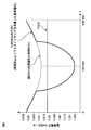
- FIG. 2 is a timing chart for explaining the delay of zero detection of the inductor current iL in the current detection circuit in the conventional example.
- Td in FIG. 2 shows the delay time of zero detection due to the delay by the operational amplifier and the noise filter. That is, due to the delay of the comparator IC and the time constant of the noise filter, the comparator starts up with a delay from the ideal current zero detection point, so that the negative current increases as shown in FIG.
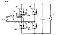
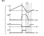
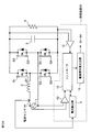
- FIG. 3A is a circuit diagram of a switching power supply device for explaining the mechanism by which the loss of the switching power supply device increases due to the delay of zero detection of the inductor current
- FIG. 3B is a timing chart showing the operation of the switching power supply device of FIG. 3A.
- the switching power supply device includes an AC power supply 1, an inductor 2, switching elements S1 to S4, a smoothing capacitor 3, and a load resistor 4.
- FIG. 3B shows an inductor current iL, a drain-source voltage Vds of the switching element S2, a drive signal G2 for the switching element S2, and a drive signal G1 for the switching element S1.
- T1 indicates a period during which soft switching is performed by the negative current of the inductor current iL.
- An object of the present invention is to solve the above problems, and in a PFC circuit operating in a current critical mode, a control circuit of a power converter capable of accurately detecting the zero point of the inductor current as compared with the prior art. And to provide the power conversion device.
- the control circuit of the power conversion device is A control circuit for a power converter that includes an inductor and includes a power factor improving circuit that operates in current critical mode.
- a first unit that detects the current of the inductor or the current corresponding to the current of the inductor or includes the current of the inductor, amplifies the voltage corresponding to the detected current with a predetermined gain, and then outputs the voltage as the detection voltage.
- a comparison circuit that compares the detected voltage with a predetermined reference voltage and outputs a comparison result signal
- a second detection circuit that detects the input voltage of the power converter, and It is provided with a third detection circuit that detects the output voltage of the power converter.
- the control circuit has the detected input voltage, the detected output voltage V, the preset delay time, the inductance value of the inductor, and the conversion coefficient when the current detected by the first detection circuit is converted into a voltage. Based on the power supply voltage and the gain of the gain, the reference voltage for detecting the zero value of the current of the inductor is calculated and output to the comparison circuit.
- the comparison circuit A first comparator that compares the detected voltage with a predetermined first reference voltage and outputs a first comparison result signal at a zero-cross detection point where the detected voltage changes from positive to negative.
- a second which compares the detected voltage with a predetermined second reference voltage lower than the first reference voltage, and outputs a second comparison result signal at a zero-cross detection point where the detected voltage changes from negative to positive.
- the first pulse generation circuit that detects the rise of the first comparison result signal and outputs the first pulse signal, and the first pulse generation circuit.
- a second pulse generation circuit that detects the rise of the second comparison result signal and outputs a second pulse signal, and A set reset type flip-flop having a set terminal, a reset terminal, and an output terminal, the first pulse signal is input to the set terminal, the second pulse signal is input to the reset terminal, and the comparison is performed from the output terminal. It is characterized by including a set reset type flip-flop that outputs a circuit comparison result signal.
- the present invention in the PFC circuit operating in the current critical mode, it is possible to prevent the detection delay of the inductor current and accurately detect the zero point of the inductor current as compared with the prior art. This reduces the loss of the power converter and leads to a higher density of the power supply device.
- FIG. 5 is a circuit diagram showing a configuration example of a switching power supply device including the control circuit 20 according to the first embodiment. It is a circuit diagram which shows the structural example of the current detection part 5 of FIG. 1A. It is a timing chart for demonstrating the delay of zero detection of an inductor current in a current detection circuit in a conventional example. It is a circuit diagram of the switching power supply device for demonstrating the mechanism that the loss of the switching power supply device increases due to the delay of zero detection of the inductor current. It is a timing chart which shows the operation of the switching power supply device of FIG. 3A. It is a circuit diagram of the switching power supply device for demonstrating the mechanism that the loss of the switching power supply device increases due to the delay of zero detection of the inductor current.
- FIG. 3C It is a timing chart which shows the operation of the switching power supply device of FIG. 3C. It is a circuit diagram which shows the structural example of the current detection part which concerns on the prior art example. It is a timing chart which shows the operation of the current detection part of FIG. 4A. It is a circuit diagram which shows the structural example of the current detection part 5 which concerns on embodiment. It is a timing chart which shows the operation of the current detection part 5 of FIG. 4C. It is a graph which shows the operation of the current detection part 5 which concerns on Embodiment 1.
- FIG. It is a block diagram which shows the structural example of the power conversion apparatus using the PFC circuit which concerns on Embodiment 1.
- FIG. It is a waveform diagram for demonstrating the derivation method of the reference voltage Vref used for the current detection part 5 which concerns on Embodiment 1.
- FIG. It is a waveform diagram for demonstrating soft switching of a PFC circuit by the current detection part 5 which concerns on Embodiment 1.
- FIG. It is a waveform diagram for demonstrating soft switching of a PFC circuit by the current detection part 5 which concerns on Embodiment 1.
- FIG. It is a waveform diagram for demonstrating the derivation method of the reference voltage Vref used for the current detection part 5 which concerns on a modification.
- FIG. It is a block diagram which shows the structural example of the switching power supply device which concerns on modification 2.
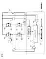
- FIG. 1A is a circuit diagram showing a configuration example of a switching power supply device including the control circuit 20 according to the first embodiment.
- the switching power supply device includes an AC power supply 1, a reactor 2 inductor, bridge-connected switching elements S1 to S4, a smoothing capacitor 3, a load resistor 4, and a shunt resistor. It includes Rs and a control circuit 20.
- the control circuit 20 includes a controller 10, a current detection unit 5, a drive signal generation circuit 11, an input voltage detection circuit 12, and an output voltage detection circuit 13.
- the input voltage Vin generated by the AC power supply 1 is input to the bridge connection circuit of the switching elements S1 to S4 via the shunt resistor Rs and the inductor 2.
- the switching elements S1 to S4 are turned on / off by the drive signals G1 to G4 from the drive signal generation circuit 11, and after the input voltage Vin is switched, the smoothed direct current is passed through the smoothing capacitor 3.
- the voltage is output to the load resistor 4 as the output voltage Vout.
- the shunt resistor Rs converts the inductor current iL into a voltage value and outputs it to the current detection unit 5.
- the input voltage detection circuit 12 detects the input voltage Vin and outputs it to the controller 10, and the output voltage detection circuit 13 detects the output voltage Vout and outputs it to the controller 10.
- the controller 10 controls the drive signal generation circuit 11 so as to generate the drive signals G1 to G4 in the current critical mode, for example, based on each input signal.
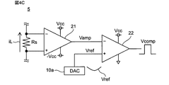
- the controller 10 includes a DA converter 10a that generates a reference voltage Vref determined in advance by a method described in detail later.
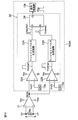
- FIG. 1B is a circuit diagram showing a configuration example of the current detection unit 5 of FIG. 1A.
- the current detection unit 5 includes an operational amplifier 21 and a comparator 22.
- Vcc is the power supply voltage.
- the operational amplifier 21 amplifies the voltage corresponding to the inductor current iL detected by the shunt resistor Rs, and outputs the amplified voltage Vamp to the comparator 22.
- the comparator 22 compares the input amplification voltage Vamp with the reference voltage Vref from the DA converter 10a in the controller 10, generates a comparison result voltage Vcomp, and outputs the comparison result voltage Vcomp to the controller 10.
- the controller 10 detects the zero current of the inductor current iL based on the comparison result voltage Vcomp, and based on this, for example, performs a switching operation in the current critical mode to generate drive signals G1 to G4.
- the drive signal generation circuit 11 is controlled so as to generate the current.
- the polarity of the reference voltage Vref is inverted according to the input voltage Vin (FIG. 1A) to the PFC circuit, that is, according to the direction of the inductor current iL.
- the detection delay can be prevented by changing the reference voltage Vref of the comparator 22 according to the delay time.
- Vref the reference voltage
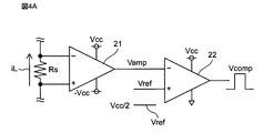
- FIG. 4A is a circuit diagram showing a configuration example of the current detection unit according to the conventional example
- FIG. 4B is a timing chart showing the operation of the current detection unit of FIG. 4A.
- the reference voltage Vref of the comparator 22 is a constant voltage such as Vcc / 2
- a delay time Tdelay occurs as shown in FIG. 4B.
- FIG. 4C is a circuit diagram showing a configuration example of the current detection unit 5 according to the first embodiment
- FIG. 4D is a timing chart showing the operation of the current detection unit 5 of FIG. 4C.
- the reference voltage Vref is raised from the DA converter 10a of the controller 10 according to the delay time. That is, in a PFC circuit in which the input voltage is alternating current, the delay time Tdelay can be reduced by changing the reference voltage Vref depending on the input voltage Vin, as shown in FIG. 4D, as compared with FIG. 4B. it can.
- Td_amp is the delay time due to the amplification operation of the operational amplifier 21.
- Td_comp is the delay time due to the comparison operation of the comparator 22.
- Tdead-time is the dead time of the switching elements S1 and S2.
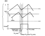
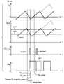
- FIG. 5 is a graph showing the operation of the current detection unit 5 according to the first embodiment.
- Vref half cycle of the input voltage Vin
- Vcc 3V
- Tdelay 50ns
- Vin (rms) 200V
- fLINE 50Hz.
- FIG. 6 is a block diagram showing a configuration example of a power conversion device using the PFC circuit according to the first embodiment.
- the power conversion device includes an AC power supply 1, a PFC circuit 100, a DC / DC converter 101, and a load 102. Since the control target is a PFC circuit, the input AC voltage and the output DC voltage are Vin (t) and Vout, respectively.
- the input voltage Vin is expressed by the following equation.
- the resistance value of the shunt resistor Rs is Rs
- the gain of the operational amplifier 21 is G
- the voltage applied to the operational amplifier 21 and the comparator 22 is Vcc.
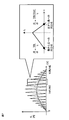
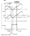
- FIG. 7 is a waveform diagram for explaining a method of deriving the reference voltage Vref used in the current detection unit 5 according to the first embodiment.
- the inductor current iL in the half cycle of the input voltage Vin is as shown in the graph of FIG. 7, and an enlarged view of one switching cycle is shown on the right side.
- the slope of the inductor current iL is obtained from win (t), Vout, and the inductance value L.
- the current fluctuation amount ⁇ idelay that changes during the delay time is expressed by the following equation.
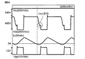
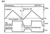
- FIG. 8A and 8B are waveform diagrams for explaining soft switching of the PFC circuit by the current detection unit 5 according to the first embodiment.
- FIG. 8A is a waveform diagram when Vin> Vout / 2
- FIG. 8B is a waveform diagram when additional on-time control is performed.
- the first embodiment is characterized in that TCM control is performed only by changing the reference voltage Vref of the comparator 22 by using a known TCM (Triangular Current Mode) control method.
- TCM Triangular Current Mode
- Vin Input voltage
- Vds Drain-source voltage of main switch element
- iL Inductor current
- Vgs Gate-source voltage of main switch element
- the controller 10 detects the detected input voltage Vin and output voltage Vout, the preset delay time, the inductance value of the inductor 2, and the resistance value of the shunt resistance Rs (in the modification described later, when the current is detected). It is a conversion coefficient when converting the inductor current iL into a voltage, and is generally the conversion coefficient.),
- the power supply voltage Vcc, and the gain of the inductor 21 are used to detect the zero value of the inductor current iL.
- the reference voltage Vref for making the delay at the time substantially zero is calculated and output to the comparator 22.
- the synchronous rectifier switch element is kept on for a predetermined additional time ⁇ [ns] from the current zero detection point to flow a negative current for extracting the electric charge.
- the soft switching method shown in FIGS. 8A and 8B allows a negative current required for soft switching to flow by continuously turning on + ⁇ [ns] and giving an additional on time.
- the negative current required for soft switching can be adjusted to flow by changing the reference voltage Vref.
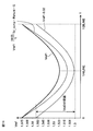
- FIG. 9 is a waveform diagram for explaining a method of deriving the reference voltage Vref used in the current detection unit 5 according to the modified example.
- the reference voltage Vref only for the delay prevention control of FIG. 5 is lowered for a predetermined time period, for example, in an elliptical shape.
- the negative current required for soft switching can be obtained from the input voltage Vin, the output voltage Vout, and the inductor tans L of the inductor 2, and can be realized by adding it to the reference voltage Vref in consideration of the delay time.
- FIG. 10A is a block diagram showing a configuration example of the switching power supply device according to the first modification.
- the inductor current iL flowing through the shunt resistor Rs is detected, but the present invention is not limited to this, and as shown in FIG. 10A, for example, a CT (Current Transformer), a Hall element, and a GMR (Giant).
- the inductor current iL may be detected by using a current sensor 14 such as a Magneto Resistive effect) element.
- FIG. 10B is a block diagram showing a configuration example of the switching power supply device according to the second modification.
- a shunt resistor Rs1 may be inserted between the ground side of the switching elements S2 and S4 and the load resistor 4, and the zero point of the inductor current iL may be detected.
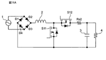
- FIG. 11A is a block diagram showing a configuration example of the switching power supply device according to the third modification.
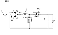
- FIG. 11A shows an example of a synchronous rectification type step-up PFC circuit.
- the switching power supply device includes an AC power supply 1, four bridge-connected diodes D1 to D4, a reactor inductor 2, switching elements S11 and S12, a shunt resistor Rs2, and a smoothing capacitor 3.
- a load resistor 4 is provided.
- a shunt resistor Rs2 for detecting the zero point of the inductor current iL is inserted between the switching element S12 and the smoothing capacitor 3. It is preferable to do so.
- FIG. 11B is a block diagram showing a configuration example of the switching power supply device according to the modified example 4.
- a shunt resistor Rs3 for detecting the zero point of the inductor current iL may be inserted between the diodes D1 and D4 and the inductor 2.
- the current corresponding to the inductor current iL or the current including the inductor current iL is detected.
- FIG. 12 is a circuit diagram showing a modified example of the current detection unit 5 of FIG. 1B.
- a controller 10A having a DA converter 10a, a comparator 22 and a signal processing unit 10b is provided.
- the signal processing unit 10b performs signal processing for changing the above-mentioned reference voltage Vref based on the comparison result signal Vcomp from the comparator 22.
- Some controllers such as DSPs (digital signal processors) have a built-in comparator function as well as AD converters and DA converters. By using the built-in comparator 22, there is an advantage that an external comparator IC becomes unnecessary.
- the delay in detecting the inductor current is prevented and the inductor current is accurately compared with the prior art.
- the zero point of the inductor current can be detected accurately. This reduces the loss of the power converter and leads to a higher density of the power supply device. In particular, since no magnetic material is used, the loss does not increase even when driven at high frequencies, and no additional parts are required. Further, by applying the method of changing the reference voltage Vref, a soft switching function using voltage resonance can be easily implemented.
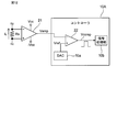
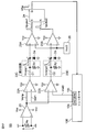
- FIG. 13 is a circuit diagram showing a configuration example of the current detection unit 5A according to the second embodiment.
- the current detection unit 5A according to the second embodiment has the following differences as compared with the current detection unit 5 in FIG. 1B.
- a comparison circuit 30 including comparators 22A and 22B, one-shot pulse generation circuits 23A and 23B, and a set reset type flip-flop 24 is provided.
- the controller 10 instead of the controller 10 having the DAC 10a, the controller 10B having the DACs 10a and 10b was provided. The above differences will be described in detail below.
- the operational amplifier 21 amplifies the voltage corresponding to the inductor current iL detected by the shunt resistor Rs, and outputs the amplified voltage Vamp to the comparators 22A and 22B.
- the controller 10B includes a DA converter 10a that generates a predetermined reference voltage Vref1 described later, and a DA converter 10c that generates a predetermined reference voltage Vref2 described later.
- the comparator 22A compares the input amplification voltage Vamp with the reference voltage Vref1 from the DA converter 10a in the controller 10B, generates a comparison result voltage Vcomp1, and outputs the comparison result voltage Vcomp1 to the one-shot pulse generation circuit 23A. Further, the comparator 22B compares the input amplification voltage Vamp2 with the reference voltage Vref2 from the DA converter 10c in the controller 10B, generates a comparison result voltage Vcomp2, and outputs the comparison result voltage Vcomp2 to the one-shot pulse generation circuit 23B.
- the voltage settings of the reference voltages Vref1 and Vref2 will be described later with reference to FIG.
- the one-shot pulse generation circuits 23A and 23B are composed of, for example, a multiplexer vibrator, and each of the one-shot pulse generation circuits 23A and 23B has one pulse in response to the rise of the comparison result voltage Vcomp1 and Vcomp2 of the input pulse signals, respectively. Is generated and output to the set terminal and the reset terminal of the set reset type flip-flop 24. In response to this, the set reset type flip-flop 24 outputs the zero cross detection pulse voltage Vflip to the controller 10B. Further, the controller 10B detects the zero current of the inductor current iL based on the zero cross detection pulse voltage Vflip, and based on this, for example, performs a switching operation in the current critical mode to generate drive signals G1 to G4. The drive signal generation circuit 11 (FIG. 1A) is controlled.
- FIG. 14 is a waveform diagram for explaining a method of deriving the reference voltages Vref1 and Vref2 used for the current detection unit 5A of FIG. 13, and FIG. 15A is a timing chart showing the operation of the current detection unit 5A of FIG.
- the reference voltage Vref1 is set to the same value as the reference voltage Vref in the first embodiment, and is set to Vcc / 2 ⁇ Vref1.
- the reference voltage Vref1 detects the timing (FIG. 7) of the zero-cross detection point (ZCD point) in which the inductor current iL changes from positive to negative, and compensates for the delay in the rise of the zero-cross detection point (ZCD point).
- the reference voltage Vref2 is set as Vref2 ⁇ Vref1 and detects the timing (FIG. 7) of the zero cross detection point (ZCD point) that changes positively from the negative of the inductor current iL, and the pulse of the zero cross detection pulse voltage Vflip. Contributes to shortening the width.
- the comparator 22A of FIG. 13 has Vref1> Vcc / 2 when the input voltage Vin (FIG. 1A) to the PFC circuit is positive, and the comparator 22A determines the timing at which the inductor current iL changes from positive to negative. It detects and outputs the comparison result voltage Vcomp1 indicating it. As a result, the rise delay of the zero-cross detection pulse voltage Vflip is eliminated. Further, the comparator 22B detects the timing at which Vref2 ⁇ Vref1 and the inductor current iL changes from negative to positive when the input voltage Vin (FIG. 1A) to the PFC circuit is positive, and the comparison result voltage indicating this is detected. Output Vcomp2.
- the fall delay of the zero-cross detection pulse voltage Vflip is eliminated.
- the case where the input voltage Vin (FIG. 1A) to the PFC circuit is positive is described, but when it is negative, the reference voltages Vref1 and Vref2 are also described in the same manner as the inversion of the reference voltage Vref described above. Inverted, the comparators 22A and 22B operate in the same manner except for the inversion of these polarities.
- FIG. 15B and 15C are diagrams for explaining the problem of the current detection unit 5 according to the first embodiment
- FIG. 15B is a waveform diagram showing an inductor current iL
- FIG. 15C is a portion of the waveform diagram of FIG. 15B. It is a timing chart of each signal and the like corresponding to 202.
- the reference voltage Vref near the zero cross point becomes relatively large.
- the slope of the inductor current iL becomes steep, and the on-time of the switching element (the time when di / dt is positive) becomes short.
- FIG. 15B inctor current iL portion 202
- FIG. 15C the fall of the comparison result voltage Vcomp is delayed, and the on state is continuously generated at the comparison result voltage Vcomp 1. There was a problem.
- the reference voltage Vref2 may be set so as to satisfy the above equation as shown in FIG.
- FIG. 16 is a circuit diagram showing a modified example of the current detection unit 5A of FIG.
- a controller 10BA having a DA converters 10a and 10b, a comparison circuit 30, and a signal processing unit 10b is provided.
- the signal processing unit 10b performs signal processing for changing the above-mentioned reference voltages Vref1 and Vref2 based on the zero-cross detection pulse voltage Vflip from the set reset type flip-flop 24.
- the current detection unit 5A of FIG. 13 according to the second embodiment may be applied to the switching power supply device according to the first to fourth modifications according to the first embodiment.
- the delay in detecting the inductor current is prevented and the inductor current is accurately compared with the prior art.
- the zero point of the inductor current can be detected accurately. This reduces the loss of the power converter and leads to a higher density of the power supply device. In particular, since no magnetic material is used, the loss does not increase even when driven at high frequencies, and no additional parts are required. Further, by applying the method of changing the reference voltage Vref, a soft switching function using voltage resonance can be easily implemented.
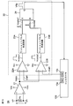
- FIG. 17 is a circuit diagram showing a configuration example of the current detection unit 5B according to the third embodiment.
- the current detection unit 5B according to the third embodiment has the following differences as compared with the current detection unit 5A according to the second embodiment.
- (1) instead of the one-shot pulse generation circuit 23A, a differentiating circuit 23C, a protection diode Da, and a comparator 25A are provided.
- (2) instead of the one-shot pulse generation circuit 23B, a differentiating circuit 23D, a protection diode Db, and a comparator 25B are provided. The differences will be described below.
- the differentiating circuit 23C includes a capacitor C1 and a resistor R1.
- the output terminal of the differentiating circuit 23C is provided with a protection diode Da that allows a negative current to flow to the ground and does not output a negative voltage.
- the differentiating voltage output from the differentiating circuit 23C is input to the comparator 25A to which the reference voltage Vcc / 2 from the reference voltage generator 26 is applied via the protection diode Da.
- the comparator 25A compares the input differential voltage with the reference voltage Vcc / 2, and outputs the comparison result voltage Vpulus 1 to the set reset type flip-flop 24.
- the differentiating circuit 23D is configured to include a capacitor C2 and a resistor R2.
- the output terminal of the differentiating circuit 23D is provided with a protection diode Db that allows a negative current to flow to the ground and does not output a negative voltage.
- the differentiating voltage output from the differentiating circuit 23D is input to the comparator 25B to which the reference voltage Vcc / 2 from the reference voltage generator 26 is applied via the protection diode Db.
- the comparator 25B compares the input differential voltage with the reference voltage Vcc / 2, and outputs the comparison result voltage Vpulus 2 to the set reset type flip-flop 24.
- the current detection unit 5B configured as described above operates in the same manner as the current detection unit 5B in FIG. 13, except for the difference in the above configuration.
- the current detection unit 5B of FIG. 17 according to the second embodiment may be applied to the switching power supply device according to the first to fourth modifications according to the first embodiment. Further, the current detection unit 5B may be configured like the controller 10BA in FIG.
- the third embodiment and the modified examples configured as described above also have the same effects as those of the first and second embodiments.
- the switching power supply device is described in the above embodiments or modifications, the present invention is not limited to this, and can be applied to various power conversion devices including the switching power supply device.
- the detection delay of the inductor current is prevented, and the zero point of the inductor current is accurately detected as compared with the prior art. can do. This reduces the loss of the power converter and leads to a higher density of the power supply device.
Landscapes
- Engineering & Computer Science (AREA)
- Power Engineering (AREA)
- Rectifiers (AREA)
- Dc-Dc Converters (AREA)
Abstract
The present invention detects the zero point of an inductor current accurately, in a power converting device that includes a PFC circuit which operates in a boundary current mode. A control circuit (20) is provided with: a current detecting unit (5, 5A) including a first detecting circuit which detects a current (iL) through an inductor, amplifies a voltage corresponding to the detected current by a prescribed gain, and then outputs the amplified voltage as a detection voltage, and a comparator circuit which compares the detection voltage with a prescribed reference voltage and outputs a comparison result signal; a second detecting circuit (12) which detects an input voltage (Vin); and a third detecting circuit (13) which detects an output voltage (Vout). The control circuit (20) calculates and outputs to the comparator circuit the reference voltage for setting to substantially zero a delay when detecting the zero value of the inductor current, on the basis of the detected input voltage, the detected output voltage, a predetermined delay time, the inductance value of the inductor, a conversion coefficient (Rs) for use when the current detected by the first detecting circuit is converted into a voltage, a power supply voltage, and the gain.
Description
本発明は、例えば力率改善回路などの電力変換装置の制御回路と、当該電力変換装置とに関する。
The present invention relates to a control circuit of a power conversion device such as a power factor improving circuit, and the power conversion device.
例えば電流臨界モードで動作する力率改善回路(以下、PFC回路という。)においては、インダクタ電流が0になってからスイッチング素子をオンする必要がある。従って、インダクタ電流のゼロ点を正確に検出する必要がある(例えば、非特許文献1参照)。
For example, in a power factor improving circuit (hereinafter referred to as a PFC circuit) that operates in the current critical mode, it is necessary to turn on the switching element after the inductor current becomes 0. Therefore, it is necessary to accurately detect the zero point of the inductor current (see, for example, Non-Patent Document 1).
従来、当該インダクタ電流の検出回路では、シャント抵抗とオペアンプ、コンパレータを用いて電流検出を行っていた(例えば、非特許文献1参照)。そのため、ICの遅延や、ノイズ除去用のフィルタでの遅延が発生して、正確にゼロ検出を行うことができないという課題があった。
Conventionally, in the inductor current detection circuit, current detection is performed using a shunt resistor, an operational amplifier, and a comparator (see, for example, Non-Patent Document 1). Therefore, there is a problem that the delay of the IC and the delay of the filter for noise removal occur, and the zero detection cannot be performed accurately.
図2は従来例における電流検出回路におけるインダクタ電流iLのゼロ検出の遅延を説明するためのタイミングチャートである。図2において、ゼロ検出用比較結果信号の理想値と現実値を図示している。図2のtdは、オペアンプ及びノイズフィルタによる遅延のためのゼロ検出の遅延時間を示す。すなわち、コンパレータICの遅延やノイズフィルタの時定数により、理想値の電流ゼロ検出点から遅れてコンパレータが立ち上がるため、図2に示すように負電流が増加する。
FIG. 2 is a timing chart for explaining the delay of zero detection of the inductor current iL in the current detection circuit in the conventional example. In FIG. 2, the ideal value and the actual value of the comparison result signal for zero detection are illustrated. Td in FIG. 2 shows the delay time of zero detection due to the delay by the operational amplifier and the noise filter. That is, due to the delay of the comparator IC and the time constant of the noise filter, the comparator starts up with a delay from the ideal current zero detection point, so that the negative current increases as shown in FIG.
図3Aは前記インダクタ電流のゼロ検出の遅延によるスイッチング電源装置の損失が増加するメカニズムを説明するためのスイッチング電源装置の回路図であり、図3Bは図3Aのスイッチング電源装置の動作を示すタイミングチャートである。図3Aにおいて、スイッチング電源装置は、交流電源1と、インダクタ2と、スイッチング素子S1~S4と、平滑用キャパシタ3と、負荷抵抗4とを備える。図3Bにおいて、インダクタ電流iLと、スイッチング素子S2のドレイン・ソース間電圧Vdsと、スイッチング素子S2に対する駆動信号G2と、スイッチング素子S1に対する駆動信号G1とを示す。ここで、T1は、インダクタ電流iLの負電流によりソフトスイッチングさせる期間を示す。
FIG. 3A is a circuit diagram of a switching power supply device for explaining the mechanism by which the loss of the switching power supply device increases due to the delay of zero detection of the inductor current, and FIG. 3B is a timing chart showing the operation of the switching power supply device of FIG. 3A. Is. In FIG. 3A, the switching power supply device includes an AC power supply 1, an inductor 2, switching elements S1 to S4, a smoothing capacitor 3, and a load resistor 4. FIG. 3B shows an inductor current iL, a drain-source voltage Vds of the switching element S2, a drive signal G2 for the switching element S2, and a drive signal G1 for the switching element S1. Here, T1 indicates a period during which soft switching is performed by the negative current of the inductor current iL.
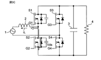
前記ソフトスイッチングによる遅延により、図3C及び図3Dに示すように、インダクタ電流iLの負電流はスイッチング素子S2のボディダイオードを流れる。この余分な負電流が流れることで、スイッチング電源装置の損失が増大する。
Due to the delay due to the soft switching, as shown in FIGS. 3C and 3D, the negative current of the inductor current iL flows through the body diode of the switching element S2. The flow of this extra negative current increases the loss of the switching power supply.
特に、小型大容量電源の開発過程においては、高周波でかつ大電流の検出を行う必要があり、それに対する解決手段が課題となっていた。
In particular, in the process of developing a small and large capacity power supply, it was necessary to detect a high frequency and a large current, and a solution to this was an issue.
本発明の目的は以上の問題点を解決し、電流臨界モードで動作するPFC回路において、従来技術に比較して正確にインダクタ電流のゼロ点を正確に検出することができる電力変換装置の制御回路及び、当該電力変換装置を提供することにある。
An object of the present invention is to solve the above problems, and in a PFC circuit operating in a current critical mode, a control circuit of a power converter capable of accurately detecting the zero point of the inductor current as compared with the prior art. And to provide the power conversion device.
本発明の一態様に係る電力変換装置の制御回路は、
インダクタを含み、電流臨界モードで動作する力率改善回路を含む電力変換装置の制御回路であって、
前記インダクタの電流、もしくは前記インダクタの電流に対応し又は前記インダクタの電流を含む電流を検出し、前記検出した電流に対応する電圧を所定の利得で増幅した後、検出電圧として出力する第1の検出回路と、
前記検出電圧を所定の基準電圧と比較して比較結果信号を出力する比較回路と、
前記電力変換装置の入力電圧を検出する第2の検出回路と、
前記電力変換装置の出力電圧を検出する第3の検出回路とを備え、
前記制御回路は、前記検出した入力電圧、前記検出した出力電圧V、予め設定された遅延時間、前記インダクタのインダクタンス値、前記第1の検出回路により検出した電流を電圧に変換するときの変換係数、電源電圧、及び前記利得の利得に基づいて、前記インダクタの電流のゼロ値を検出するときの遅延を実質的にゼロにするための基準電圧を計算して前記比較回路に出力し、
前記比較回路は、
前記検出電圧を所定の第1の基準電圧と比較し、前記検出電圧が正から負に変化するゼロクロス検出点で第1の比較結果信号を出力する第1の比較器と、
前記検出電圧を前記第1の基準電圧よりも低い所定の第2の基準電圧と比較し、前記検出電圧が負から正に変化するゼロクロス検出点で第2の比較結果信号を出力する第2の比較器と、
前記第1の比較結果信号の立ち上がりを検出して第1のパルス信号を出力する第1のパルス生成回路と、
前記第2の比較結果信号の立ち上がりを検出して第2のパルス信号を出力する第2のパルス生成回路と、
セット端子、リセット端子及び出力端子を有するセットリセット型フリップフロップであって、前記第1のパルス信号をセット端子に入力し、前記第2のパルス信号をリセット端子に入力し、出力端子から前記比較回路の比較結果信号を出力するセットリセット型フリップフロップとを備えることを特徴とする。 The control circuit of the power conversion device according to one aspect of the present invention is
A control circuit for a power converter that includes an inductor and includes a power factor improving circuit that operates in current critical mode.
A first unit that detects the current of the inductor or the current corresponding to the current of the inductor or includes the current of the inductor, amplifies the voltage corresponding to the detected current with a predetermined gain, and then outputs the voltage as the detection voltage. With the detection circuit
A comparison circuit that compares the detected voltage with a predetermined reference voltage and outputs a comparison result signal,
A second detection circuit that detects the input voltage of the power converter, and
It is provided with a third detection circuit that detects the output voltage of the power converter.
The control circuit has the detected input voltage, the detected output voltage V, the preset delay time, the inductance value of the inductor, and the conversion coefficient when the current detected by the first detection circuit is converted into a voltage. Based on the power supply voltage and the gain of the gain, the reference voltage for detecting the zero value of the current of the inductor is calculated and output to the comparison circuit.
The comparison circuit
A first comparator that compares the detected voltage with a predetermined first reference voltage and outputs a first comparison result signal at a zero-cross detection point where the detected voltage changes from positive to negative.
A second, which compares the detected voltage with a predetermined second reference voltage lower than the first reference voltage, and outputs a second comparison result signal at a zero-cross detection point where the detected voltage changes from negative to positive. With a comparator,
The first pulse generation circuit that detects the rise of the first comparison result signal and outputs the first pulse signal, and the first pulse generation circuit.
A second pulse generation circuit that detects the rise of the second comparison result signal and outputs a second pulse signal, and
A set reset type flip-flop having a set terminal, a reset terminal, and an output terminal, the first pulse signal is input to the set terminal, the second pulse signal is input to the reset terminal, and the comparison is performed from the output terminal. It is characterized by including a set reset type flip-flop that outputs a circuit comparison result signal.
従って、本発明によれば、電流臨界モードで動作するPFC回路において、インダクタ電流の検出遅延を防止して、従来技術に比較して正確にインダクタ電流のゼロ点を正確に検出することができる。これにより、電力変換装置の損失が低減され、電源装置の高密度化につながる。
Therefore, according to the present invention, in the PFC circuit operating in the current critical mode, it is possible to prevent the detection delay of the inductor current and accurately detect the zero point of the inductor current as compared with the prior art. This reduces the loss of the power converter and leads to a higher density of the power supply device.
以下、本発明に係る実施形態について図面を参照して説明する。なお、同一又は同様の構成要素については同一の符号を付している。
Hereinafter, embodiments according to the present invention will be described with reference to the drawings. The same or similar components are designated by the same reference numerals.
(実施形態1)
図1Aは実施形態1に係る制御回路20を備えたスイッチング電源装置の構成例を示す回路図である。 (Embodiment 1)
FIG. 1A is a circuit diagram showing a configuration example of a switching power supply device including the control circuit 20 according to the first embodiment.
図1Aは実施形態1に係る制御回路20を備えたスイッチング電源装置の構成例を示す回路図である。 (Embodiment 1)
FIG. 1A is a circuit diagram showing a configuration example of a switching power supply device including the control circuit 20 according to the first embodiment.
図1Aにおいて、本実施形態に係るスイッチング電源装置は、交流電源1と、リアクトルであるインダクタ2と、ブリッジ接続されたスイッチング素子S1~S4と、平滑用キャパシタ3と、負荷抵抗4と、シャント抵抗Rsと、制御回路20とを備える。ここで、制御回路20は、コントローラ10と、電流検出部5と、駆動信号発生回路11と、入力電圧検出回路12と、出力電圧検出回路13とを備える。
In FIG. 1A, the switching power supply device according to the present embodiment includes an AC power supply 1, a reactor 2 inductor, bridge-connected switching elements S1 to S4, a smoothing capacitor 3, a load resistor 4, and a shunt resistor. It includes Rs and a control circuit 20. Here, the control circuit 20 includes a controller 10, a current detection unit 5, a drive signal generation circuit 11, an input voltage detection circuit 12, and an output voltage detection circuit 13.
交流電源1により発生された入力電圧Vinは、シャント抵抗Rs及びインダクタ2を介して、スイッチング素子S1~S4のブリッジ接続回路に入力される。各スイッチング素子S1~S4は駆動信号発生回路11からの駆動信号G1~G4によりオン/オフ制御されることで、入力電圧Vinがスイッチングされた後、平滑用キャパシタ3を介して、平滑された直流電圧が出力電圧Voutとして負荷抵抗4に出力される。
The input voltage Vin generated by the AC power supply 1 is input to the bridge connection circuit of the switching elements S1 to S4 via the shunt resistor Rs and the inductor 2. The switching elements S1 to S4 are turned on / off by the drive signals G1 to G4 from the drive signal generation circuit 11, and after the input voltage Vin is switched, the smoothed direct current is passed through the smoothing capacitor 3. The voltage is output to the load resistor 4 as the output voltage Vout.
シャント抵抗Rsはインダクタ電流iLを電圧値に変換して電流検出部5に出力する。入力電圧検出回路12は入力電圧Vinを検出してコントローラ10に出力し、出力電圧検出回路13は出力電圧Voutを検出してコントローラ10に出力する。コントローラ10は、入力される各信号に基づいて、例えば電流臨界モードで駆動信号G1~G4を発生するように駆動信号発生回路11を制御する。なお、コントローラ10は、詳細後述する方法で予め決められる基準電圧Vrefを発生するDA変換器10aを備える。
The shunt resistor Rs converts the inductor current iL into a voltage value and outputs it to the current detection unit 5. The input voltage detection circuit 12 detects the input voltage Vin and outputs it to the controller 10, and the output voltage detection circuit 13 detects the output voltage Vout and outputs it to the controller 10. The controller 10 controls the drive signal generation circuit 11 so as to generate the drive signals G1 to G4 in the current critical mode, for example, based on each input signal. The controller 10 includes a DA converter 10a that generates a reference voltage Vref determined in advance by a method described in detail later.
図1Bは図1Aの電流検出部5の構成例を示す回路図である。図1Bにおいて、電流検出部5は、オペアンプ21と、コンパレータ22とを備えて構成される。なお、Vccは電源電圧である。
FIG. 1B is a circuit diagram showing a configuration example of the current detection unit 5 of FIG. 1A. In FIG. 1B, the current detection unit 5 includes an operational amplifier 21 and a comparator 22. Vcc is the power supply voltage.
オペアンプ21は、シャント抵抗Rsにより検出されたインダクタ電流iLに対応する電圧を増幅し、増幅電圧Vampをコンパレータ22に出力する。コンパレータ22は、入力される増幅電圧Vampを、コントローラ10内のDA変換器10aからの基準電圧Vrefと比較して、比較結果電圧Vcompを発生してコントローラ10に出力する。これに応答して、コントローラ10は、比較結果電圧Vcompに基づいて、インダクタ電流iLのゼロ電流を検出し、これに基づいて、例えば電流臨界モードでのスイッチング動作をさせて駆動信号G1~G4を発生するように駆動信号発生回路11を制御する。なお、基準電圧Vrefの極性は、PFC回路への入力電圧Vin(図1A)に応じて、すなわち、インダクタ電流iLの向きに応じて反転される。
The operational amplifier 21 amplifies the voltage corresponding to the inductor current iL detected by the shunt resistor Rs, and outputs the amplified voltage Vamp to the comparator 22. The comparator 22 compares the input amplification voltage Vamp with the reference voltage Vref from the DA converter 10a in the controller 10, generates a comparison result voltage Vcomp, and outputs the comparison result voltage Vcomp to the controller 10. In response to this, the controller 10 detects the zero current of the inductor current iL based on the comparison result voltage Vcomp, and based on this, for example, performs a switching operation in the current critical mode to generate drive signals G1 to G4. The drive signal generation circuit 11 is controlled so as to generate the current. The polarity of the reference voltage Vref is inverted according to the input voltage Vin (FIG. 1A) to the PFC circuit, that is, according to the direction of the inductor current iL.
以上のように構成された制御回路20を備えたスイッチング電源装置によれば、コンパレータ22の基準電圧Vrefを遅延時間に応じて変化させることで、検出遅延を防止することができる。これにより、臨界モードPFC回路におけるインダクタ電流iLのゼロ点検出遅延による効率悪化を防止することができる。以下、本実施形態の作用効果について詳述する。
According to the switching power supply device provided with the control circuit 20 configured as described above, the detection delay can be prevented by changing the reference voltage Vref of the comparator 22 according to the delay time. As a result, it is possible to prevent efficiency deterioration due to the zero point detection delay of the inductor current iL in the critical mode PFC circuit. Hereinafter, the effects of the present embodiment will be described in detail.
図4Aは従来例に係る電流検出部の構成例を示す回路図であり、図4Bは図4Aの電流検出部の動作を示すタイミングチャートである。図4Aに示すように、コンパレータ22の基準電圧Vrefが例えばVcc/2等の一定電圧では、図4Bに示すように、遅延時間Tdelayが発生する。
FIG. 4A is a circuit diagram showing a configuration example of the current detection unit according to the conventional example, and FIG. 4B is a timing chart showing the operation of the current detection unit of FIG. 4A. As shown in FIG. 4A, when the reference voltage Vref of the comparator 22 is a constant voltage such as Vcc / 2, a delay time Tdelay occurs as shown in FIG. 4B.
図4Cは実施形態1に係る電流検出部5の構成例を示す回路図であり、図4Dは図4Cの電流検出部5の動作を示すタイミングチャートである。図4Cに示すように、コントローラ10のDA変換器10aから、基準電圧Vrefを遅延時間に応じて上昇させる。すなわち、入力電圧が交流であるPFC回路において、入力電圧Vinに依存して基準電圧Vrefを変化させることで、図4Dに示すように、図4Bとの比較により、遅延時間Tdelayを減少させることができる。なお、図4Dにおいて、
(1)Td_ampはオペアンプ21の増幅動作による遅延時間であり、
(2)Td_compはコンパレータ22の比較動作による遅延時間であり、
(3)Tdead-timeはスイッチング素子S1,S2のデッドタイムである。 FIG. 4C is a circuit diagram showing a configuration example of thecurrent detection unit 5 according to the first embodiment, and FIG. 4D is a timing chart showing the operation of the current detection unit 5 of FIG. 4C. As shown in FIG. 4C, the reference voltage Vref is raised from the DA converter 10a of the controller 10 according to the delay time. That is, in a PFC circuit in which the input voltage is alternating current, the delay time Tdelay can be reduced by changing the reference voltage Vref depending on the input voltage Vin, as shown in FIG. 4D, as compared with FIG. 4B. it can. In addition, in FIG. 4D,
(1) Td_amp is the delay time due to the amplification operation of theoperational amplifier 21.
(2) Td_comp is the delay time due to the comparison operation of thecomparator 22.
(3) Tdead-time is the dead time of the switching elements S1 and S2.
(1)Td_ampはオペアンプ21の増幅動作による遅延時間であり、
(2)Td_compはコンパレータ22の比較動作による遅延時間であり、
(3)Tdead-timeはスイッチング素子S1,S2のデッドタイムである。 FIG. 4C is a circuit diagram showing a configuration example of the
(1) Td_amp is the delay time due to the amplification operation of the
(2) Td_comp is the delay time due to the comparison operation of the
(3) Tdead-time is the dead time of the switching elements S1 and S2.
図5は実施形態1に係る電流検出部5の動作を示すグラフである。図5において、例えば、Vcc=3V,Tdelay=50ns,Vin(rms)=200V,fLINE=50Hzのときの基準電圧Vref(入力電圧Vinの半周期)の一例を図示している。図1B及び図5Cの電流検出部5及び個年と10を用いることで、遅延時間Tdelayから導出された基準電圧Vrefを、電流検出部5のコンパレータ22に帰還して入力することで、遅延時間Tdelayを減少させることができる。
FIG. 5 is a graph showing the operation of the current detection unit 5 according to the first embodiment. FIG. 5 shows an example of a reference voltage Vref (half cycle of the input voltage Vin) when, for example, Vcc = 3V, Tdelay = 50ns, Vin (rms) = 200V, and fLINE = 50Hz. By using the current detection unit 5 and the year and 10 of FIGS. 1B and 5C, the reference voltage Vref derived from the delay time Tdeli is returned to the comparator 22 of the current detection unit 5 and input to the delay time. Tdelay can be reduced.
以下、基準電圧Vrefの導出方法の一例について以下に説明する。
Hereinafter, an example of a method for deriving the reference voltage Vref will be described below.
図6は実施形態1に係るPFC回路を用いた電力変換装置の構成例を示すブロック図である。図6において、電力変換装置は、交流電源1と、PFC回路100と、DC/DCコンバータ101と、負荷102とを備えて構成される。制御対象はPFC回路であるため、入力交流電圧及び出力直流電圧であり、それぞれVin(t)、Voutとする。入力電圧Vinは次式で表される。
FIG. 6 is a block diagram showing a configuration example of a power conversion device using the PFC circuit according to the first embodiment. In FIG. 6, the power conversion device includes an AC power supply 1, a PFC circuit 100, a DC / DC converter 101, and a load 102. Since the control target is a PFC circuit, the input AC voltage and the output DC voltage are Vin (t) and Vout, respectively. The input voltage Vin is expressed by the following equation.
ここで、入力電圧Vin(rms)及びライン周波数fLINEは国や地域によって異なり、それらの一例は以下の通りである。
Vin(rms)=100V,200V,230V
fLINE=50Hz、又は60Hz Here, the input voltage Vin (rms) and the line frequency fLINE differ depending on the country or region, and an example thereof is as follows.
Vin (rms) = 100V, 200V, 230V
fLINE = 50Hz or 60Hz
Vin(rms)=100V,200V,230V
fLINE=50Hz、又は60Hz Here, the input voltage Vin (rms) and the line frequency fLINE differ depending on the country or region, and an example thereof is as follows.
Vin (rms) = 100V, 200V, 230V
fLINE = 50Hz or 60Hz
図1B及び図4Cの電流検出部5を用いたとき、シャント抵抗Rsの抵抗値をRsとし、オペアンプ21の利得をGとし、オペアンプ21及びコンパレータ22に印加する電圧をVccとする。
When the current detection unit 5 of FIGS. 1B and 4C is used, the resistance value of the shunt resistor Rs is Rs, the gain of the operational amplifier 21 is G, and the voltage applied to the operational amplifier 21 and the comparator 22 is Vcc.
図7は実施形態1に係る電流検出部5に用いる基準電圧Vrefの導出方法を説明するための波形図である。
FIG. 7 is a waveform diagram for explaining a method of deriving the reference voltage Vref used in the current detection unit 5 according to the first embodiment.
入力電圧Vinの半周期におけるインダクタ電流iLは、図7のグラフのようになり、1スイッチンング周期分を抜き出した拡大図を右側に図示する。ここで、インダクタ電流iLの傾きはvin(t)、Vout、インダクタンス値Lにより求められる。電流ゼロの検出遅延時間Tdelayに基づいて、遅延時間中に変化する電流変動量Δidelayは次式で表される。
The inductor current iL in the half cycle of the input voltage Vin is as shown in the graph of FIG. 7, and an enlarged view of one switching cycle is shown on the right side. Here, the slope of the inductor current iL is obtained from win (t), Vout, and the inductance value L. Based on the detection delay time Tdelay of zero current, the current fluctuation amount Δidelay that changes during the delay time is expressed by the following equation.
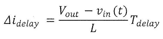
この電流変動量Δidelayだけ、早く電流ゼロを検出すればよい。当該電流変動量Δidelayに対してシャント抵抗の抵抗値Rs及びオペアンプ21の利得Gを乗算することで電圧に変換できるので、遅延時間を考慮した基準電圧Vrefは次式で表される。
It is sufficient to detect zero current as soon as this current fluctuation amount Δidelay. Since the voltage can be converted by multiplying the current fluctuation amount Δidelay by the resistance value Rs of the shunt resistor and the gain G of the operational amplifier 21, the reference voltage Vref considering the delay time is expressed by the following equation.

図8A及び図8Bは実施形態1に係る電流検出部5によるPFC回路のソフトスイッチングを説明するための波形図である。ここで、図8AはVin>Vout/2のときの波形図であり、図8Bは追加オン時間制御のときの波形図である。
8A and 8B are waveform diagrams for explaining soft switching of the PFC circuit by the current detection unit 5 according to the first embodiment. Here, FIG. 8A is a waveform diagram when Vin> Vout / 2, and FIG. 8B is a waveform diagram when additional on-time control is performed.
本実施形態1では、公知のTCM(Triangular Current Mode)制御方法を用いて、コンパレータ22の基準電圧Vrefを変化させるのみでTCM制御を行うことを特徴としている。図8A及び図8Bにおいて、各符号は以下の通りである。
Vin:入力電圧
Vds:メインスイッチ素子のドレイン・ソース間電圧
iL:インダクタ電流
Vgs:メインスイッチ素子のゲート・ソース間電圧 The first embodiment is characterized in that TCM control is performed only by changing the reference voltage Vref of thecomparator 22 by using a known TCM (Triangular Current Mode) control method. In FIGS. 8A and 8B, the reference numerals are as follows.
Vin: Input voltage Vds: Drain-source voltage of main switch element iL: Inductor current Vgs: Gate-source voltage of main switch element
Vin:入力電圧
Vds:メインスイッチ素子のドレイン・ソース間電圧
iL:インダクタ電流
Vgs:メインスイッチ素子のゲート・ソース間電圧 The first embodiment is characterized in that TCM control is performed only by changing the reference voltage Vref of the
Vin: Input voltage Vds: Drain-source voltage of main switch element iL: Inductor current Vgs: Gate-source voltage of main switch element
以上の実施形態1では、コントローラ10は、検出した入力電圧Vin及び出力電圧Vout、予め設定された遅延時間、インダクタ2のインダクタンス値、シャント抵抗Rsの抵抗値(後述する変形例では、電流検出時のインダクタ電流iLを電圧に変換するときの変換係数であり、一般的には、当該変換係数である。)、電源電圧Vcc、オペアンプ21の利得に基づいて、インダクタ電流iLのゼロ値を検出するときの遅延を実質的にゼロにするための基準電圧Vrefを計算してコンパレータ22に出力する。これにより、電流臨界モードで動作するPFC回路を備えた電力変換装置において、インダクタ電流の検出遅延を防止して、従来技術に比較して正確にインダクタ電流のゼロ点を正確に検出することができる。
In the first embodiment, the controller 10 detects the detected input voltage Vin and output voltage Vout, the preset delay time, the inductance value of the inductor 2, and the resistance value of the shunt resistance Rs (in the modification described later, when the current is detected). It is a conversion coefficient when converting the inductor current iL into a voltage, and is generally the conversion coefficient.), The power supply voltage Vcc, and the gain of the inductor 21 are used to detect the zero value of the inductor current iL. The reference voltage Vref for making the delay at the time substantially zero is calculated and output to the comparator 22. As a result, in a power converter equipped with a PFC circuit that operates in the current critical mode, it is possible to prevent a delay in detecting the inductor current and accurately detect the zero point of the inductor current as compared with the prior art. ..
図8AのVin>Vout/2の条件下では、スイッチング素子の電荷を引き抜くための負電流が足りずソフトスイッチングできない。従って、TCM制御方法を用いて、同期整流スイッチ素子を、電流ゼロ検出点から所定の追加時間α[ns]だけオンし続けることによって電荷を引き抜くための負電流を流す。
Under the condition of Vin> Vout / 2 in FIG. 8A, soft switching is not possible due to insufficient negative current for extracting the charge of the switching element. Therefore, using the TCM control method, the synchronous rectifier switch element is kept on for a predetermined additional time α [ns] from the current zero detection point to flow a negative current for extracting the electric charge.
図8A及び図8Bで図示したソフトスイッチング手法は+α[ns]オンし続けて追加オン時間を与えることでソフトスイッチングに必要な負電流を流す。しかしながら、図9を参照して以下に示すように、基準電圧Vrefを変化させることでソフトスイッチングに必要な負電流を流すように調整することもできる。
The soft switching method shown in FIGS. 8A and 8B allows a negative current required for soft switching to flow by continuously turning on + α [ns] and giving an additional on time. However, as shown below with reference to FIG. 9, the negative current required for soft switching can be adjusted to flow by changing the reference voltage Vref.
図9は変形例に係る電流検出部5に用いる基準電圧Vrefの導出方法を説明するための波形図である。図9に示すように、図5の遅延防止制御のみの基準電圧Vrefに対して、所定の時間期間のみ例えば楕円形状で低下させる。ここで、ソフトスイッチングに必要な負電流は入力電圧Vin、出力電圧Vout及びインダクタ2のインダクタタンスLより求めることができ、遅延時間を考慮した基準電圧Vrefに追加することで実現できる。
FIG. 9 is a waveform diagram for explaining a method of deriving the reference voltage Vref used in the current detection unit 5 according to the modified example. As shown in FIG. 9, the reference voltage Vref only for the delay prevention control of FIG. 5 is lowered for a predetermined time period, for example, in an elliptical shape. Here, the negative current required for soft switching can be obtained from the input voltage Vin, the output voltage Vout, and the inductor tans L of the inductor 2, and can be realized by adding it to the reference voltage Vref in consideration of the delay time.
図10Aは変形例1に係るスイッチング電源装置の構成例を示すブロック図である。図1Aの実施形態1では、シャント抵抗Rsに流れるインダクタ電流iLを検出しているが、本発明はこれに限らず、図10Aのように、例えばCT(Current Transformer)、ホール素子、GMR(Giant Magneto Resistive effect)素子等の電流センサ14を用いてインダクタ電流iLを検出してもよい。
FIG. 10A is a block diagram showing a configuration example of the switching power supply device according to the first modification. In the first embodiment of FIG. 1A, the inductor current iL flowing through the shunt resistor Rs is detected, but the present invention is not limited to this, and as shown in FIG. 10A, for example, a CT (Current Transformer), a Hall element, and a GMR (Giant). The inductor current iL may be detected by using a current sensor 14 such as a Magneto Resistive effect) element.
図10Bは変形例2に係るスイッチング電源装置の構成例を示すブロック図である。図10Bにおいて、スイッチング素子S2,S4の接地側と負荷抵抗4との間にシャント抵抗Rs1を挿入して、インダクタ電流iLがゼロ点を検出してもよい。
FIG. 10B is a block diagram showing a configuration example of the switching power supply device according to the second modification. In FIG. 10B, a shunt resistor Rs1 may be inserted between the ground side of the switching elements S2 and S4 and the load resistor 4, and the zero point of the inductor current iL may be detected.
図11Aは変形例3に係るスイッチング電源装置の構成例を示すブロック図である。図11Aは同期整流方式昇圧型PFC回路の一例を示している。図11Aにおいて、スイッチング電源装置は、交流電源1と、ブリッジ接続の4個のダイオードD1~D4と、リアクトルであるインダクタ2と、スイッチング素子S11,S12と、シャント抵抗Rs2と、平滑用キャパシタ3と、負荷抵抗4とを備えて構成される。図11Aにおいては、同期整流方式昇圧型PFC回路において、本実施形態を適用した場合は、スイッチング素子S12と平滑用キャパシタ3との間に、インダクタ電流iLのゼロ点を検出するシャント抵抗Rs2を挿入することが好ましい。
FIG. 11A is a block diagram showing a configuration example of the switching power supply device according to the third modification. FIG. 11A shows an example of a synchronous rectification type step-up PFC circuit. In FIG. 11A, the switching power supply device includes an AC power supply 1, four bridge-connected diodes D1 to D4, a reactor inductor 2, switching elements S11 and S12, a shunt resistor Rs2, and a smoothing capacitor 3. , A load resistor 4 is provided. In FIG. 11A, in the synchronous rectification type step-up PFC circuit, when this embodiment is applied, a shunt resistor Rs2 for detecting the zero point of the inductor current iL is inserted between the switching element S12 and the smoothing capacitor 3. It is preferable to do so.
図11Bは変形例4に係るスイッチング電源装置の構成例を示すブロック図である。図11Bの変形例4では、図11Aの変形例3に代えて、ダイオードD1,D4とインダクタ2との間に、インダクタ電流iLのゼロ点を検出するシャント抵抗Rs3を挿入してもよい。
FIG. 11B is a block diagram showing a configuration example of the switching power supply device according to the modified example 4. In the modified example 4 of FIG. 11B, instead of the modified example 3 of FIG. 11A, a shunt resistor Rs3 for detecting the zero point of the inductor current iL may be inserted between the diodes D1 and D4 and the inductor 2.
以上の変形例2~4においては、インダクタ電流iLに対応する電流又はインダクタ電流iLを含む電流を検出するように構成している。
In the above modified examples 2 to 4, the current corresponding to the inductor current iL or the current including the inductor current iL is detected.
図12は図1Bの電流検出部5の変形例を示す回路図である。図12において、コントローラ10に代えて、DA変換器10a、コンパレータ22及び信号処理部10bを有するコントローラ10Aを備えたことを特徴とする。ここで、信号処理部10bはコンパレータ22からの比較結果信号Vcompに基づいて、上述の基準電圧Vrefを変更する信号処理を行う。
FIG. 12 is a circuit diagram showing a modified example of the current detection unit 5 of FIG. 1B. In FIG. 12, instead of the controller 10, a controller 10A having a DA converter 10a, a comparator 22 and a signal processing unit 10b is provided. Here, the signal processing unit 10b performs signal processing for changing the above-mentioned reference voltage Vref based on the comparison result signal Vcomp from the comparator 22.
DSP(デジタル・シグナル・プロセッサ)などのコントローラには、AD変換器、DA変換器だけでなく、コンパレータの機能も内蔵しているものがある。内蔵のコンパレータ22を使用することで外付けのコンパレータICが不要になるという利点がある。
Some controllers such as DSPs (digital signal processors) have a built-in comparator function as well as AD converters and DA converters. By using the built-in comparator 22, there is an advantage that an external comparator IC becomes unnecessary.
以上説明したように、実施形態1及び変形例によれば、電流臨界モードで動作するPFC回路を備えた電力変換装置において、インダクタ電流の検出遅延を防止して、従来技術に比較して正確にインダクタ電流のゼロ点を正確に検出することができる。これにより、電力変換装置の損失が低減され、電源装置の高密度化につながる。特に、磁性体を使用しないので高周波駆動した際も損失が増加せず、追加部品が必要ない。また、基準電圧Vrefを変化させる手法を応用すれば、電圧共振を使用したソフトスイッチング機能を簡単に実装できる。
As described above, according to the first embodiment and the modified example, in the power conversion device provided with the PFC circuit operating in the current critical mode, the delay in detecting the inductor current is prevented and the inductor current is accurately compared with the prior art. The zero point of the inductor current can be detected accurately. This reduces the loss of the power converter and leads to a higher density of the power supply device. In particular, since no magnetic material is used, the loss does not increase even when driven at high frequencies, and no additional parts are required. Further, by applying the method of changing the reference voltage Vref, a soft switching function using voltage resonance can be easily implemented.
(実施形態2)
図13は実施形態2に係る電流検出部5Aの構成例を示す回路図である。図13において、実施形態2に係る電流検出部5Aは、図1Bの電流検出部5に比較して以下の相違点を有する。
(1)コンパレータ22に代えて、コンパレータ22A,22B、ワンショットパルス生成回路23A,23B、及びセットリセット型フリップフロップ24を備えた比較回路30を備えた。
(2)DAC10aを有するコントローラ10に代えて、DAC10a,10bを有するコントローラ10Bを備えた。
以下、上記の相違点について詳述する。 (Embodiment 2)
FIG. 13 is a circuit diagram showing a configuration example of thecurrent detection unit 5A according to the second embodiment. In FIG. 13, the current detection unit 5A according to the second embodiment has the following differences as compared with the current detection unit 5 in FIG. 1B.
(1) Instead of thecomparator 22, a comparison circuit 30 including comparators 22A and 22B, one-shot pulse generation circuits 23A and 23B, and a set reset type flip-flop 24 is provided.
(2) Instead of thecontroller 10 having the DAC 10a, the controller 10B having the DACs 10a and 10b was provided.
The above differences will be described in detail below.
図13は実施形態2に係る電流検出部5Aの構成例を示す回路図である。図13において、実施形態2に係る電流検出部5Aは、図1Bの電流検出部5に比較して以下の相違点を有する。
(1)コンパレータ22に代えて、コンパレータ22A,22B、ワンショットパルス生成回路23A,23B、及びセットリセット型フリップフロップ24を備えた比較回路30を備えた。
(2)DAC10aを有するコントローラ10に代えて、DAC10a,10bを有するコントローラ10Bを備えた。
以下、上記の相違点について詳述する。 (Embodiment 2)
FIG. 13 is a circuit diagram showing a configuration example of the
(1) Instead of the
(2) Instead of the
The above differences will be described in detail below.
図13において、オペアンプ21は、シャント抵抗Rsにより検出されたインダクタ電流iLに対応する電圧を増幅し、増幅電圧Vampをコンパレータ22A,22Bに出力する。コントローラ10Bは、後述する所定の基準電圧Vref1を発生するDA変換器10aと、後述する所定の基準電圧Vref2を発生するDA変換器10cとを備える。
In FIG. 13, the operational amplifier 21 amplifies the voltage corresponding to the inductor current iL detected by the shunt resistor Rs, and outputs the amplified voltage Vamp to the comparators 22A and 22B. The controller 10B includes a DA converter 10a that generates a predetermined reference voltage Vref1 described later, and a DA converter 10c that generates a predetermined reference voltage Vref2 described later.
コンパレータ22Aは、入力される増幅電圧Vampを、コントローラ10B内のDA変換器10aからの基準電圧Vref1と比較して、比較結果電圧Vcomp1を発生してワンショットパルス生成回路23Aに出力する。また、コンパレータ22Bは、入力される増幅電圧Vamp2を、コントローラ10B内のDA変換器10cからの基準電圧Vref2と比較して、比較結果電圧Vcomp2を発生してワンショットパルス生成回路23Bに出力する。ここで、基準電圧Vref1,Vref2の電圧設定は図14を参照して後述する。
The comparator 22A compares the input amplification voltage Vamp with the reference voltage Vref1 from the DA converter 10a in the controller 10B, generates a comparison result voltage Vcomp1, and outputs the comparison result voltage Vcomp1 to the one-shot pulse generation circuit 23A. Further, the comparator 22B compares the input amplification voltage Vamp2 with the reference voltage Vref2 from the DA converter 10c in the controller 10B, generates a comparison result voltage Vcomp2, and outputs the comparison result voltage Vcomp2 to the one-shot pulse generation circuit 23B. Here, the voltage settings of the reference voltages Vref1 and Vref2 will be described later with reference to FIG.
ワンショットパルス生成回路23A,23Bは例えばマルチプレクサバイブレータで構成され、各ワンショットパルス生成回路23A,23Bはそれぞれ、入力されるパルス信号の比較結果電圧Vcomp1,Vcomp2の立ち上がりに応答して1個のパルスを発生してセットリセット型フリップフロップ24のセット端子及びリセット端子に出力する。これに応答して、セットリセット型フリップフロップ24はゼロクロス検出パルス電圧Vflipをコントローラ10Bに出力する。さらに、コントローラ10Bは、ゼロクロス検出パルス電圧Vflipに基づいて、インダクタ電流iLのゼロ電流を検出し、これに基づいて、例えば電流臨界モードでのスイッチング動作をさせて駆動信号G1~G4を発生するように駆動信号発生回路11(図1A)を制御する。
The one-shot pulse generation circuits 23A and 23B are composed of, for example, a multiplexer vibrator, and each of the one-shot pulse generation circuits 23A and 23B has one pulse in response to the rise of the comparison result voltage Vcomp1 and Vcomp2 of the input pulse signals, respectively. Is generated and output to the set terminal and the reset terminal of the set reset type flip-flop 24. In response to this, the set reset type flip-flop 24 outputs the zero cross detection pulse voltage Vflip to the controller 10B. Further, the controller 10B detects the zero current of the inductor current iL based on the zero cross detection pulse voltage Vflip, and based on this, for example, performs a switching operation in the current critical mode to generate drive signals G1 to G4. The drive signal generation circuit 11 (FIG. 1A) is controlled.
図14は図13の電流検出部5Aに用いる基準電圧Vref1,Vref2の導出方法を説明するための波形図であり、図15Aは図13の電流検出部5Aの動作を示すタイミングチャートである。
FIG. 14 is a waveform diagram for explaining a method of deriving the reference voltages Vref1 and Vref2 used for the current detection unit 5A of FIG. 13, and FIG. 15A is a timing chart showing the operation of the current detection unit 5A of FIG.
図14に示すように、基準電圧Vref1は実施形態1における基準電圧Vrefと同一の値に設定され、Vcc/2<Vref1に設定される。ここで、基準電圧Vref1は、インダクタ電流iLの正から負に変化するゼロクロス検出点(ZCD点)のタイミング(図7)を検出して、ゼロクロス検出点(ZCD点)の立ち上がりの遅延を補償する。一方、基準電圧Vref2はVref2<Vref1のように設定され、インダクタ電流iLの負から正に変化するゼロクロス検出点(ZCD点)のタイミング(図7)を検出して、ゼロクロス検出パルス電圧Vflipのパルス幅を短くすることに貢献する。
As shown in FIG. 14, the reference voltage Vref1 is set to the same value as the reference voltage Vref in the first embodiment, and is set to Vcc / 2 <Vref1. Here, the reference voltage Vref1 detects the timing (FIG. 7) of the zero-cross detection point (ZCD point) in which the inductor current iL changes from positive to negative, and compensates for the delay in the rise of the zero-cross detection point (ZCD point). .. On the other hand, the reference voltage Vref2 is set as Vref2 <Vref1 and detects the timing (FIG. 7) of the zero cross detection point (ZCD point) that changes positively from the negative of the inductor current iL, and the pulse of the zero cross detection pulse voltage Vflip. Contributes to shortening the width.
すなわち、図13のコンパレータ22Aは、PFC回路への入力電圧Vin(図1A)が正極性のとき、Vref1>Vcc/2であり、コンパレータ22Aは、インダクタ電流iLの正から負に変化するタイミングを検出し、それを示す比較結果電圧Vcomp1を出力する。これにより、ゼロクロス検出パルス電圧Vflipの立ち上がり遅延を解消する。また、コンパレータ22Bは、PFC回路への入力電圧Vin(図1A)が正極性のとき、Vref2<Vref1であり、インダクタ電流iLの負から正に変化するタイミングを検出し、それを示す比較結果電圧Vcomp2を出力する。これにより、ゼロクロス検出パルス電圧Vflipの立ち下がり遅延を解消する。なお、ここで、PFC回路への入力電圧Vin(図1A)が正極性のときについて説明しているが、負極性のときは上述の基準電圧Vrefの反転と同様に、基準電圧Vref1,Vref2も反転され、コンパレータ22A,22Bは、これら極性の反転を除いて同様に動作する。
That is, the comparator 22A of FIG. 13 has Vref1> Vcc / 2 when the input voltage Vin (FIG. 1A) to the PFC circuit is positive, and the comparator 22A determines the timing at which the inductor current iL changes from positive to negative. It detects and outputs the comparison result voltage Vcomp1 indicating it. As a result, the rise delay of the zero-cross detection pulse voltage Vflip is eliminated. Further, the comparator 22B detects the timing at which Vref2 <Vref1 and the inductor current iL changes from negative to positive when the input voltage Vin (FIG. 1A) to the PFC circuit is positive, and the comparison result voltage indicating this is detected. Output Vcomp2. As a result, the fall delay of the zero-cross detection pulse voltage Vflip is eliminated. Here, the case where the input voltage Vin (FIG. 1A) to the PFC circuit is positive is described, but when it is negative, the reference voltages Vref1 and Vref2 are also described in the same manner as the inversion of the reference voltage Vref described above. Inverted, the comparators 22A and 22B operate in the same manner except for the inversion of these polarities.
基準電圧Vref1の場合、図7の「ゼロクロス検出点」を正確に検出する必要があるため正確な計算で導出した(実施形態1)が、基準電圧Vref2の役割はゼロクロス検出パルス電圧Vflipのパルス幅を短くする(図15Aの201)ことなので、正確に図7の「負から正に変化するゼロクロス検出点(ZCD点)に合わせる必要はない。
In the case of the reference voltage Vref1, since it is necessary to accurately detect the "zero cross detection point" in FIG. 7, it was derived by accurate calculation (Embodiment 1), but the role of the reference voltage Vref2 is the pulse width of the zero cross detection pulse voltage Vflip. Is shortened (201 in FIG. 15A), so it is not necessary to accurately match the “zero cross detection point (ZCD point) changing from negative to positive” in FIG. 7.
図15B及び図15Cは実施形態1に係る電流検出部5の課題を説明するための図であって、図15Bはインダクタ電流iLを示す波形図であり、図15Cは図15Bの波形図の部分202に対応する各信号等のタイミングチャートである。実施形態1に係る図5から明らかなように、ゼロクロス点付近の基準電圧Vrefは相対的に大きくなる。また、高周波駆動の場合は、インダクタンス値Lが比較的小さいため、インダクタ電流iLの傾きが急になり、スイッチング素子のオン時間(di/dtが正の時間)が短くなる。その結果、図15B(インダクタ電流iLの部分202)及び図15Cに示すように、比較結果電圧Vcompの立下がりが遅延して、比較結果電圧Vcompにおいて連続的にオン状態が発生するという実施形態1の課題があった。
15B and 15C are diagrams for explaining the problem of the current detection unit 5 according to the first embodiment, FIG. 15B is a waveform diagram showing an inductor current iL, and FIG. 15C is a portion of the waveform diagram of FIG. 15B. It is a timing chart of each signal and the like corresponding to 202. As is clear from FIG. 5 according to the first embodiment, the reference voltage Vref near the zero cross point becomes relatively large. Further, in the case of high frequency drive, since the inductance value L is relatively small, the slope of the inductor current iL becomes steep, and the on-time of the switching element (the time when di / dt is positive) becomes short. As a result, as shown in FIG. 15B (inductor current iL portion 202) and FIG. 15C, the fall of the comparison result voltage Vcomp is delayed, and the on state is continuously generated at the comparison result voltage Vcomp 1. There was a problem.
上述のように、正確に図7の「負から正に変化するゼロクロス検出点(ZCD点)に合わせる必要はないが、ただし、図15B及び図15Cに示すようコンパレータ22A,22Bの遅延時間Td_comp分だけは早める必要があるので、次式を満たすように設定すれば、図15Aに示すように2回のオン状態を防止できる。
As described above, it is not necessary to exactly match the “zero cross detection point (ZCD point) changing from negative to positive” in FIG. 7, but as shown in FIGS. 15B and 15C, the delay times Td_comp of the comparators 22A and 22B. Since it is necessary to accelerate the speed, it is possible to prevent the two ON states as shown in FIG. 15A by setting so as to satisfy the following equation.

上式とVref2<Vref1の関係を満たせば、基準電圧Vref2は例えば、
(1)Vref2=Vcc/2、もしくは
(2)Vref2=Vref1-(定数)
など、どの様な値に設定してもよい。また、電流臨界モード(CRM)で動作するPFC回路の場合、インダクタ電流iLは、入力されるAC電圧が正極性のとき、ほとんど負側に流れないので、基準電圧Vref2は以下の範囲に設定するのが妥当である If the relationship between the above equation and Vref2 <Vref1 is satisfied, the reference voltage Vref2 is, for example,
(1) Vref2 = Vcc / 2, or (2) Vref2 = Vref1- (constant)
Any value may be set. Further, in the case of a PFC circuit operating in the current critical mode (CRM), the inductor current iL hardly flows to the negative side when the input AC voltage is positive, so the reference voltage Vref2 is set in the following range. Is reasonable

以上説明したように、本実施形態において、基準電圧Vref2は、図14に示すように、上式を満たすように設定すればよい。
As described above, in the present embodiment, the reference voltage Vref2 may be set so as to satisfy the above equation as shown in FIG.
図16は図13の電流検出部5Aの変形例を示す回路図である。図16において、コントローラ10Bに代えて、DA変換器10a,10b、比較回路30、及び信号処理部10bを有するコントローラ10BAを備えたことを特徴とする。ここで、信号処理部10bはセットリセット型フリップフロップ24からのゼロクロス検出パルス電圧Vflipに基づいて、上述の基準電圧Vref1,Vref2を変更する信号処理を行う。
FIG. 16 is a circuit diagram showing a modified example of the current detection unit 5A of FIG. In FIG. 16, instead of the controller 10B, a controller 10BA having a DA converters 10a and 10b, a comparison circuit 30, and a signal processing unit 10b is provided. Here, the signal processing unit 10b performs signal processing for changing the above-mentioned reference voltages Vref1 and Vref2 based on the zero-cross detection pulse voltage Vflip from the set reset type flip-flop 24.
なお、実施形態1に係る変形例1~4に係るスイッチング電源装置において、実施形態2に係る図13の電流検出部5Aを適用してもよい。
The current detection unit 5A of FIG. 13 according to the second embodiment may be applied to the switching power supply device according to the first to fourth modifications according to the first embodiment.
以上説明したように、実施形態2及び変形例によれば、電流臨界モードで動作するPFC回路を備えた電力変換装置において、インダクタ電流の検出遅延を防止して、従来技術に比較して正確にインダクタ電流のゼロ点を正確に検出することができる。これにより、電力変換装置の損失が低減され、電源装置の高密度化につながる。特に、磁性体を使用しないので高周波駆動した際も損失が増加せず、追加部品が必要ない。また、基準電圧Vrefを変化させる手法を応用すれば、電圧共振を使用したソフトスイッチング機能を簡単に実装できる。
As described above, according to the second embodiment and the modified example, in the power conversion device provided with the PFC circuit operating in the current critical mode, the delay in detecting the inductor current is prevented and the inductor current is accurately compared with the prior art. The zero point of the inductor current can be detected accurately. This reduces the loss of the power converter and leads to a higher density of the power supply device. In particular, since no magnetic material is used, the loss does not increase even when driven at high frequencies, and no additional parts are required. Further, by applying the method of changing the reference voltage Vref, a soft switching function using voltage resonance can be easily implemented.
(実施形態3)
図17は実施形態3に係る電流検出部5Bの構成例を示す回路図である。図17において、実施形態3に係る電流検出部5Bは、実施形態2に係る電流検出部5Aに比較して以下の相違点がある。
(1)ワンショットパルス生成回路23Aに代えて、微分回路23C、保護ダイオードDa及びコンパレータ25Aの回路を備えた。
(2)ワンショットパルス生成回路23Bに代えて、微分回路23D、保護ダイオードDb及びコンパレータ25Bの回路を備えた。
以下、前記相違点について説明する。 (Embodiment 3)
FIG. 17 is a circuit diagram showing a configuration example of thecurrent detection unit 5B according to the third embodiment. In FIG. 17, the current detection unit 5B according to the third embodiment has the following differences as compared with the current detection unit 5A according to the second embodiment.
(1) Instead of the one-shotpulse generation circuit 23A, a differentiating circuit 23C, a protection diode Da, and a comparator 25A are provided.
(2) Instead of the one-shotpulse generation circuit 23B, a differentiating circuit 23D, a protection diode Db, and a comparator 25B are provided.
The differences will be described below.
図17は実施形態3に係る電流検出部5Bの構成例を示す回路図である。図17において、実施形態3に係る電流検出部5Bは、実施形態2に係る電流検出部5Aに比較して以下の相違点がある。
(1)ワンショットパルス生成回路23Aに代えて、微分回路23C、保護ダイオードDa及びコンパレータ25Aの回路を備えた。
(2)ワンショットパルス生成回路23Bに代えて、微分回路23D、保護ダイオードDb及びコンパレータ25Bの回路を備えた。
以下、前記相違点について説明する。 (Embodiment 3)
FIG. 17 is a circuit diagram showing a configuration example of the
(1) Instead of the one-shot
(2) Instead of the one-shot
The differences will be described below.
図17において、微分回路23CはキャパシタC1及び抵抗R1を備えて構成される。微分回路23Cの出力端子に、負電流を接地に流して負電圧を出力しない保護ダイオードDaを備える。微分回路23Cから出力される微分電圧は保護ダイオードDaを介して、基準電圧発生器26からの基準電圧Vcc/2が印加されたコンパレータ25Aに入力される。コンパレータ25Aは、入力される微分電圧を基準電圧Vcc/2と比較して、比較結果電圧Vpulse1をセットリセット型フリップフロップ24に出力する。
In FIG. 17, the differentiating circuit 23C includes a capacitor C1 and a resistor R1. The output terminal of the differentiating circuit 23C is provided with a protection diode Da that allows a negative current to flow to the ground and does not output a negative voltage. The differentiating voltage output from the differentiating circuit 23C is input to the comparator 25A to which the reference voltage Vcc / 2 from the reference voltage generator 26 is applied via the protection diode Da. The comparator 25A compares the input differential voltage with the reference voltage Vcc / 2, and outputs the comparison result voltage Vpulus 1 to the set reset type flip-flop 24.
微分回路23DはキャパシタC2及び抵抗R2を備えて構成される。微分回路23Dの出力端子に、負電流を接地に流して負電圧を出力しない保護ダイオードDbを備える。微分回路23Dから出力される微分電圧は保護ダイオードDbを介して、基準電圧発生器26からの基準電圧Vcc/2が印加されたコンパレータ25Bに入力される。コンパレータ25Bは、入力される微分電圧を基準電圧Vcc/2と比較して、比較結果電圧Vpulse2をセットリセット型フリップフロップ24に出力する。
The differentiating circuit 23D is configured to include a capacitor C2 and a resistor R2. The output terminal of the differentiating circuit 23D is provided with a protection diode Db that allows a negative current to flow to the ground and does not output a negative voltage. The differentiating voltage output from the differentiating circuit 23D is input to the comparator 25B to which the reference voltage Vcc / 2 from the reference voltage generator 26 is applied via the protection diode Db. The comparator 25B compares the input differential voltage with the reference voltage Vcc / 2, and outputs the comparison result voltage Vpulus 2 to the set reset type flip-flop 24.
以上のように構成された電流検出部5Bは、上記の構成の違いを除いて、図13の電流検出部5Bと同様に動作する。
The current detection unit 5B configured as described above operates in the same manner as the current detection unit 5B in FIG. 13, except for the difference in the above configuration.
なお、実施形態1に係る変形例1~4に係るスイッチング電源装置において、実施形態2に係る図17の電流検出部5Bを適用してもよい。また、電流検出部5Bを図16のコントローラ10BAのごとく構成してもよい。
The current detection unit 5B of FIG. 17 according to the second embodiment may be applied to the switching power supply device according to the first to fourth modifications according to the first embodiment. Further, the current detection unit 5B may be configured like the controller 10BA in FIG.
以上のように構成された実施形態3及び変形例においても、実施形態1及び2と同様の作用効果を有する。
The third embodiment and the modified examples configured as described above also have the same effects as those of the first and second embodiments.
(適用例)
以上の実施形態又は変形例においては、スイッチング電源装置について説明しているが、本発明はこれに限らず、スイッチング電源装置を含む種々の電力変換装置に適用することができる。 (Application example)
Although the switching power supply device is described in the above embodiments or modifications, the present invention is not limited to this, and can be applied to various power conversion devices including the switching power supply device.
以上詳述したように、本発明によれば、電流臨界モードで動作するPFC回路において、インダクタ電流の検出遅延を防止して、従来技術に比較して正確にインダクタ電流のゼロ点を正確に検出することができる。これにより、電力変換装置の損失が低減され、電源装置の高密度化につながる。
As described in detail above, according to the present invention, in the PFC circuit operating in the current critical mode, the detection delay of the inductor current is prevented, and the zero point of the inductor current is accurately detected as compared with the prior art. can do. This reduces the loss of the power converter and leads to a higher density of the power supply device.
1 交流電源
2 インダクタ
3 平滑用キャパシタ
4 負荷抵抗
5,5A,5B 電流検出部
10,10A,10B、10BA コントローラ
10a,10c DA変換器(DAC)
10b 信号処理部
11 駆動信号発生回路
12 入力電圧検出回路
13 出力電圧検出回路
14 電流センサ
20 制御回路
21 オペアンプ
22,22A,22B コンパレータ
23A,23B ワンショットパルス生成回路
23C,23D 微分回路
24 セットリセット型フリップフロップ
25S,25B コンパレータ
26 基準電圧発生器
30 比較回路
100 PFC回路
101 DC/DCコンバータ
102 負荷
C1,C2 キャパシタ
D1~D4 ダイオード
Da,Db 保護ダイオード
R1,R2 抵抗
Rs,Rs1,Rs2,Rs3 シャント抵抗
S1~S4,S11,S12 スイッチング素子 1AC power supply 2 Inductor 3 Smoothing capacitor 4 Load resistance 5, 5A, 5B Current detector 10, 10A, 10B, 10BA Controller 10a, 10c DA converter (DAC)
10bSignal processing unit 11 Drive signal generation circuit 12 Input voltage detection circuit 13 Output voltage detection circuit 14 Current sensor 20 Control circuit 21 Operational amplifier 22, 22A, 22B Comparitor 23A, 23B One-shot pulse generation circuit 23C, 23D Differentiation circuit 24 Set reset type Flip flop 25S, 25B Comparator 26 Reference voltage generator 30 Comparison circuit 100 PFC circuit 101 DC / DC converter 102 Load C1, C2 Capacitors D1 to D4 Diodes Da, Db Protection diodes R1, R2 Resistance Rs, Rs1, Rs2, Rs3 Shunt resistance S1 to S4, S11, S12 switching element
2 インダクタ
3 平滑用キャパシタ
4 負荷抵抗
5,5A,5B 電流検出部
10,10A,10B、10BA コントローラ
10a,10c DA変換器(DAC)
10b 信号処理部
11 駆動信号発生回路
12 入力電圧検出回路
13 出力電圧検出回路
14 電流センサ
20 制御回路
21 オペアンプ
22,22A,22B コンパレータ
23A,23B ワンショットパルス生成回路
23C,23D 微分回路
24 セットリセット型フリップフロップ
25S,25B コンパレータ
26 基準電圧発生器
30 比較回路
100 PFC回路
101 DC/DCコンバータ
102 負荷
C1,C2 キャパシタ
D1~D4 ダイオード
Da,Db 保護ダイオード
R1,R2 抵抗
Rs,Rs1,Rs2,Rs3 シャント抵抗
S1~S4,S11,S12 スイッチング素子 1
10b
Claims (6)
- インダクタを含み、電流臨界モードで動作する力率改善回路を含む電力変換装置の制御回路であって、
前記インダクタの電流、もしくは前記インダクタの電流に対応し又は前記インダクタの電流を含む電流を検出し、前記検出した電流に対応する電圧を所定の利得で増幅した後、検出電圧として出力する第1の検出回路と、
前記検出電圧を所定の基準電圧と比較して比較結果信号を出力する比較回路と、
前記電力変換装置の入力電圧を検出する第2の検出回路と、
前記電力変換装置の出力電圧を検出する第3の検出回路とを備え、
前記制御回路は、前記検出した入力電圧、前記検出した出力電圧V、予め設定された遅延時間、前記インダクタのインダクタンス値、前記第1の検出回路により検出した電流を電圧に変換するときの変換係数、電源電圧、及び前記利得の利得に基づいて、前記インダクタの電流のゼロ値を検出するときの遅延を実質的にゼロにするための基準電圧を計算して前記比較回路に出力し、
前記比較回路は、
前記検出電圧を所定の第1の基準電圧と比較し、前記検出電圧が正から負に変化するゼロクロス検出点で第1の比較結果信号を出力する第1の比較器と、
前記検出電圧を前記第1の基準電圧よりも低い所定の第2の基準電圧と比較し、前記検出電圧が負から正に変化するゼロクロス検出点で第2の比較結果信号を出力する第2の比較器と、
前記第1の比較結果信号の立ち上がりを検出して第1のパルス信号を出力する第1のパルス生成回路と、
前記第2の比較結果信号の立ち上がりを検出して第2のパルス信号を出力する第2のパルス生成回路と、
セット端子、リセット端子及び出力端子を有するセットリセット型フリップフロップであって、前記第1のパルス信号をセット端子に入力し、前記第2のパルス信号をリセット端子に入力し、出力端子から前記比較回路の比較結果信号を出力するセットリセット型フリップフロップとを備えることを特徴とする電力変換装置の制御回路。 A control circuit for a power converter that includes an inductor and includes a power factor improving circuit that operates in current critical mode.
A first unit that detects the current of the inductor or the current corresponding to the current of the inductor or includes the current of the inductor, amplifies the voltage corresponding to the detected current with a predetermined gain, and then outputs the voltage as the detection voltage. With the detection circuit
A comparison circuit that compares the detected voltage with a predetermined reference voltage and outputs a comparison result signal,
A second detection circuit that detects the input voltage of the power converter, and
It is provided with a third detection circuit that detects the output voltage of the power converter.
The control circuit has the detected input voltage, the detected output voltage V, the preset delay time, the inductance value of the inductor, and the conversion coefficient when the current detected by the first detection circuit is converted into a voltage. Based on the power supply voltage and the gain of the gain, the reference voltage for detecting the zero value of the current of the inductor is calculated and output to the comparison circuit.
The comparison circuit
A first comparator that compares the detected voltage with a predetermined first reference voltage and outputs a first comparison result signal at a zero-cross detection point where the detected voltage changes from positive to negative.
A second, which compares the detected voltage with a predetermined second reference voltage lower than the first reference voltage, and outputs a second comparison result signal at a zero-cross detection point where the detected voltage changes from negative to positive. With a comparator,
The first pulse generation circuit that detects the rise of the first comparison result signal and outputs the first pulse signal, and the first pulse generation circuit.
A second pulse generation circuit that detects the rise of the second comparison result signal and outputs a second pulse signal, and
A set reset type flip-flop having a set terminal, a reset terminal, and an output terminal, in which the first pulse signal is input to the set terminal, the second pulse signal is input to the reset terminal, and the comparison is performed from the output terminal. A control circuit of a power conversion device, which comprises a set reset type flip-flop that outputs a circuit comparison result signal. - 前記第1のパルス生成回路は、前記第1の比較結果信号を微分する第1の微分回路と、前記第1の微分回路に接続されかつ負電圧を出力しない第1の保護ダイオードとを備え、
前記第2のパルス生成回路は、前記第2の比較結果信号を微分する第2の微分回路と、前記第2の微分回路に接続されかつ負電圧を出力しない第2の保護ダイオードと、
前記第1の保護ダイオードから出力される電圧を、電源電圧の半分の電圧と比較して比較結果信号を前記第1のパルス信号として出力する第3の比較器と、
前記第2の保護ダイオードから出力される電圧を、前記電源電圧の半分の電圧と比較して比較結果信号を前記第2のパルス信号として出力する第4の比較器とを備えることを特徴とする請求項1記載の電力変換装置の制御回路。 The first pulse generation circuit includes a first differentiating circuit that differentiates the first comparison result signal and a first protection diode that is connected to the first differentiating circuit and does not output a negative voltage.
The second pulse generation circuit includes a second differentiating circuit that differentiates the second comparison result signal, a second protective diode that is connected to the second differentiating circuit and does not output a negative voltage, and the like.
A third comparator that compares the voltage output from the first protection diode with a voltage that is half the power supply voltage and outputs a comparison result signal as the first pulse signal.
It is characterized by including a fourth comparator that compares the voltage output from the second protection diode with a voltage that is half of the power supply voltage and outputs a comparison result signal as the second pulse signal. The control circuit of the power conversion device according to claim 1. - 前記制御回路は、前記電力変換装置のソフトスッチングに必要な負電流を考慮して前記基準電圧を計算する、
請求項1又は2記載の電力変換装置の制御回路。 The control circuit calculates the reference voltage in consideration of the negative current required for soft switching of the power converter.
The control circuit of the power conversion device according to claim 1 or 2. - 前記制御回路は、前記第1の検出回路により変換された電圧をDA変換するDA変換器を内蔵する、
請求項1~3のうちのいずれか1つに記載の電力変換装置の制御回路。 The control circuit includes a DA converter that DA-converts the voltage converted by the first detection circuit.
The control circuit of the power conversion device according to any one of claims 1 to 3. - 請求項1~4のうちのいずれか1つに記載の電力変換装置の制御回路を備える、
電力変換装置。 The control circuit of the power conversion device according to any one of claims 1 to 4 is provided.
Power converter. - 前記電力変換装置はスイッチング電源装置又はDC/DC変換装置である、
請求項5記載の電力変換装置。 The power conversion device is a switching power supply device or a DC / DC conversion device.
The power conversion device according to claim 5.
Priority Applications (3)
| Application Number | Priority Date | Filing Date | Title |
|---|---|---|---|
| CN202080052723.XA CN114144967A (en) | 2019-08-09 | 2020-07-27 | Control circuit for power conversion device and power conversion device |
| US17/629,259 US12068672B2 (en) | 2019-08-09 | 2020-07-27 | Control circuit for power converter apparatus provided with PFC circuit operating in current-critical mode |
| EP20852941.2A EP4012909A4 (en) | 2019-08-09 | 2020-07-27 | Control circuit for power converting device, and power converting device |
Applications Claiming Priority (2)
| Application Number | Priority Date | Filing Date | Title |
|---|---|---|---|
| JP2019147052A JP7293968B2 (en) | 2019-08-09 | 2019-08-09 | CONTROL CIRCUIT FOR POWER CONVERTER AND POWER CONVERTER |
| JP2019-147052 | 2019-08-09 |
Publications (1)
| Publication Number | Publication Date |
|---|---|
| WO2021029208A1 true WO2021029208A1 (en) | 2021-02-18 |
Family
ID=74569422
Family Applications (1)
| Application Number | Title | Priority Date | Filing Date |
|---|---|---|---|
| PCT/JP2020/028679 WO2021029208A1 (en) | 2019-08-09 | 2020-07-27 | Control circuit for power converting device, and power converting device |
Country Status (5)
| Country | Link |
|---|---|
| US (1) | US12068672B2 (en) |
| EP (1) | EP4012909A4 (en) |
| JP (1) | JP7293968B2 (en) |
| CN (1) | CN114144967A (en) |
| WO (1) | WO2021029208A1 (en) |
Families Citing this family (2)
| Publication number | Priority date | Publication date | Assignee | Title |
|---|---|---|---|---|
| CN115242076A (en) * | 2021-04-25 | 2022-10-25 | 华为数字能源技术有限公司 | Control system and method of totem-pole power factor correction circuit and power adapter |
| CN114089024B (en) * | 2022-01-20 | 2022-04-26 | 成都齐碳科技有限公司 | Current measuring circuit, measuring method and nanopore sequencing device |
Citations (3)
| Publication number | Priority date | Publication date | Assignee | Title |
|---|---|---|---|---|
| JP2011244583A (en) * | 2010-05-18 | 2011-12-01 | Cosel Co Ltd | Switching power supply device |
| JP2014018012A (en) * | 2012-07-11 | 2014-01-30 | Toyota Industries Corp | On-vehicle switching power supply device |
| JP2015035851A (en) * | 2013-08-07 | 2015-02-19 | 株式会社村田製作所 | Switching power supply device |
Family Cites Families (12)
| Publication number | Priority date | Publication date | Assignee | Title |
|---|---|---|---|---|
| US7902803B2 (en) * | 2005-03-04 | 2011-03-08 | The Regents Of The University Of Colorado | Digital current mode controller |
| CN102308462B (en) * | 2009-03-24 | 2014-07-02 | 株式会社村田制作所 | Switching power supply device |
| ITMI20120089A1 (en) * | 2012-01-26 | 2013-07-27 | Dora Spa | CONTROL DEVICE FOR A SWITCHING FEEDER. |
| US9287798B2 (en) * | 2012-12-06 | 2016-03-15 | Stmicroelectronics, Inc. | High power factor primary regulated offline LED driver |
| US9209689B2 (en) * | 2013-11-19 | 2015-12-08 | Terralux, Inc. | Output regulation with nonlinear digital control loop compensation |
| EP3200336B1 (en) * | 2014-09-26 | 2023-10-04 | Mitsubishi Electric Corporation | Power conversion device |
| JP6439484B2 (en) * | 2015-02-17 | 2018-12-19 | 富士電機株式会社 | Switching power supply circuit and power factor correction circuit |
| CN110048597B (en) * | 2018-01-15 | 2021-01-15 | 株式会社村田制作所 | Control method, controller and system of power factor correction circuit |
| JP6962259B2 (en) * | 2018-04-11 | 2021-11-05 | Tdk株式会社 | Switching power supply |
| JP7211018B2 (en) * | 2018-11-05 | 2023-01-24 | 富士電機株式会社 | power control unit |
| CN109713889B (en) * | 2019-01-30 | 2021-04-13 | 成都芯源系统有限公司 | Power factor correction circuit and control method thereof |
| CN112003454A (en) * | 2019-05-27 | 2020-11-27 | 恩智浦美国有限公司 | Bridgeless power factor correction converter with zero current detection circuit |
-
2019
- 2019-08-09 JP JP2019147052A patent/JP7293968B2/en active Active
-
2020
- 2020-07-27 US US17/629,259 patent/US12068672B2/en active Active
- 2020-07-27 CN CN202080052723.XA patent/CN114144967A/en active Pending
- 2020-07-27 EP EP20852941.2A patent/EP4012909A4/en active Pending
- 2020-07-27 WO PCT/JP2020/028679 patent/WO2021029208A1/en unknown
Patent Citations (3)
| Publication number | Priority date | Publication date | Assignee | Title |
|---|---|---|---|---|
| JP2011244583A (en) * | 2010-05-18 | 2011-12-01 | Cosel Co Ltd | Switching power supply device |
| JP2014018012A (en) * | 2012-07-11 | 2014-01-30 | Toyota Industries Corp | On-vehicle switching power supply device |
| JP2015035851A (en) * | 2013-08-07 | 2015-02-19 | 株式会社村田製作所 | Switching power supply device |
Non-Patent Citations (2)
| Title |
|---|
| QINGYUN HUANG ET AL.: "Predictive ZVS Control with Improved ZVS Time Margin and Limited Variable Frequency Range for A 99% Efficient, 130W/in3 MHz GaN Totem-Pole PFC Rectifier", IEEE TRANSACTIONS ON POWER ELECTRONICS, vol. 34, no. 7, 2018 |
| See also references of EP4012909A4 |
Also Published As
| Publication number | Publication date |
|---|---|
| US12068672B2 (en) | 2024-08-20 |
| CN114144967A (en) | 2022-03-04 |
| EP4012909A1 (en) | 2022-06-15 |
| JP7293968B2 (en) | 2023-06-20 |
| US20220255415A1 (en) | 2022-08-11 |
| JP2021027788A (en) | 2021-02-22 |
| EP4012909A4 (en) | 2023-08-02 |
Similar Documents
| Publication | Publication Date | Title |
|---|---|---|
| JP5182375B2 (en) | PFC converter | |
| EP2506413B1 (en) | Interleaved power converter and controller therefor | |
| US20100097828A1 (en) | Interleave control power supply device and control circuit and control method for the power supply device | |
| CN108233696B (en) | Apparatus and method for controlling pulse width modulation switching frequency | |
| KR20120020080A (en) | Method and apparatus for bridgeless power factor correction | |
| US20180006577A1 (en) | Switching power converters controlled with control signals having variable on-times | |
| WO2021029208A1 (en) | Control circuit for power converting device, and power converting device | |
| JP6607495B2 (en) | Power converter | |
| US20170366098A1 (en) | Current-sensing and gain-switching circuit and method for using wide range of current | |
| KR20170080518A (en) | Power factor correction circuit and driving method thereof | |
| US20170025969A1 (en) | Synchronous rectifier phase control to improve load efficiency | |
| JP2015171196A (en) | Power conversion device | |
| JP7226287B2 (en) | DC power supply and control method for DC power supply | |
| US9991817B2 (en) | Power converting device that uses a sine-wave-shaped current control range to output drive signal | |
| US11791718B2 (en) | Power converting device | |
| WO2021028972A1 (en) | Control circuit for power conversion device | |
| JP6395316B2 (en) | Switching power supply | |
| JP5933418B2 (en) | Power converter | |
| JP2021027788A5 (en) | ||
| EP3424140B1 (en) | Buck-boost controller achieving high power factor and valley switching | |
| CN110754032B (en) | AC-DC conversion | |
| KR20200078110A (en) | Bipolar pulse power supply circuit | |
| KR101905345B1 (en) | Power conversion device | |
| US20210184566A1 (en) | Power converter | |
| TWI667873B (en) | DC-DC converter circuit architecture with current estimation circuit |
Legal Events
| Date | Code | Title | Description |
|---|---|---|---|
| 121 | Ep: the epo has been informed by wipo that ep was designated in this application |
Ref document number: 20852941 Country of ref document: EP Kind code of ref document: A1 |
|
| NENP | Non-entry into the national phase |
Ref country code: DE |
|
| ENP | Entry into the national phase |
Ref document number: 2020852941 Country of ref document: EP Effective date: 20220309 |