JP7211018B2 - power control unit - Google Patents
power control unit Download PDFInfo
- Publication number
- JP7211018B2 JP7211018B2 JP2018208270A JP2018208270A JP7211018B2 JP 7211018 B2 JP7211018 B2 JP 7211018B2 JP 2018208270 A JP2018208270 A JP 2018208270A JP 2018208270 A JP2018208270 A JP 2018208270A JP 7211018 B2 JP7211018 B2 JP 7211018B2
- Authority
- JP
- Japan
- Prior art keywords
- voltage
- value
- switching element
- delay
- inductor
- Prior art date
- Legal status (The legal status is an assumption and is not a legal conclusion. Google has not performed a legal analysis and makes no representation as to the accuracy of the status listed.)
- Active
Links
Images


Classifications
-
- H—ELECTRICITY
- H02—GENERATION; CONVERSION OR DISTRIBUTION OF ELECTRIC POWER
- H02M—APPARATUS FOR CONVERSION BETWEEN AC AND AC, BETWEEN AC AND DC, OR BETWEEN DC AND DC, AND FOR USE WITH MAINS OR SIMILAR POWER SUPPLY SYSTEMS; CONVERSION OF DC OR AC INPUT POWER INTO SURGE OUTPUT POWER; CONTROL OR REGULATION THEREOF
- H02M3/00—Conversion of dc power input into dc power output
- H02M3/02—Conversion of dc power input into dc power output without intermediate conversion into ac
- H02M3/04—Conversion of dc power input into dc power output without intermediate conversion into ac by static converters
- H02M3/10—Conversion of dc power input into dc power output without intermediate conversion into ac by static converters using discharge tubes with control electrode or semiconductor devices with control electrode
- H02M3/145—Conversion of dc power input into dc power output without intermediate conversion into ac by static converters using discharge tubes with control electrode or semiconductor devices with control electrode using devices of a triode or transistor type requiring continuous application of a control signal
- H02M3/155—Conversion of dc power input into dc power output without intermediate conversion into ac by static converters using discharge tubes with control electrode or semiconductor devices with control electrode using devices of a triode or transistor type requiring continuous application of a control signal using semiconductor devices only
- H02M3/156—Conversion of dc power input into dc power output without intermediate conversion into ac by static converters using discharge tubes with control electrode or semiconductor devices with control electrode using devices of a triode or transistor type requiring continuous application of a control signal using semiconductor devices only with automatic control of output voltage or current, e.g. switching regulators
-
- H—ELECTRICITY
- H02—GENERATION; CONVERSION OR DISTRIBUTION OF ELECTRIC POWER
- H02M—APPARATUS FOR CONVERSION BETWEEN AC AND AC, BETWEEN AC AND DC, OR BETWEEN DC AND DC, AND FOR USE WITH MAINS OR SIMILAR POWER SUPPLY SYSTEMS; CONVERSION OF DC OR AC INPUT POWER INTO SURGE OUTPUT POWER; CONTROL OR REGULATION THEREOF
- H02M1/00—Details of apparatus for conversion
- H02M1/42—Circuits or arrangements for compensating for or adjusting power factor in converters or inverters
- H02M1/4208—Arrangements for improving power factor of AC input
- H02M1/4225—Arrangements for improving power factor of AC input using a non-isolated boost converter
-
- H—ELECTRICITY
- H02—GENERATION; CONVERSION OR DISTRIBUTION OF ELECTRIC POWER
- H02M—APPARATUS FOR CONVERSION BETWEEN AC AND AC, BETWEEN AC AND DC, OR BETWEEN DC AND DC, AND FOR USE WITH MAINS OR SIMILAR POWER SUPPLY SYSTEMS; CONVERSION OF DC OR AC INPUT POWER INTO SURGE OUTPUT POWER; CONTROL OR REGULATION THEREOF
- H02M1/00—Details of apparatus for conversion
- H02M1/08—Circuits specially adapted for the generation of control voltages for semiconductor devices incorporated in static converters
-
- H—ELECTRICITY
- H02—GENERATION; CONVERSION OR DISTRIBUTION OF ELECTRIC POWER
- H02M—APPARATUS FOR CONVERSION BETWEEN AC AND AC, BETWEEN AC AND DC, OR BETWEEN DC AND DC, AND FOR USE WITH MAINS OR SIMILAR POWER SUPPLY SYSTEMS; CONVERSION OF DC OR AC INPUT POWER INTO SURGE OUTPUT POWER; CONTROL OR REGULATION THEREOF
- H02M3/00—Conversion of dc power input into dc power output
- H02M3/22—Conversion of dc power input into dc power output with intermediate conversion into ac
- H02M3/24—Conversion of dc power input into dc power output with intermediate conversion into ac by static converters
- H02M3/28—Conversion of dc power input into dc power output with intermediate conversion into ac by static converters using discharge tubes with control electrode or semiconductor devices with control electrode to produce the intermediate ac
- H02M3/325—Conversion of dc power input into dc power output with intermediate conversion into ac by static converters using discharge tubes with control electrode or semiconductor devices with control electrode to produce the intermediate ac using devices of a triode or a transistor type requiring continuous application of a control signal
- H02M3/335—Conversion of dc power input into dc power output with intermediate conversion into ac by static converters using discharge tubes with control electrode or semiconductor devices with control electrode to produce the intermediate ac using devices of a triode or a transistor type requiring continuous application of a control signal using semiconductor devices only
- H02M3/33507—Conversion of dc power input into dc power output with intermediate conversion into ac by static converters using discharge tubes with control electrode or semiconductor devices with control electrode to produce the intermediate ac using devices of a triode or a transistor type requiring continuous application of a control signal using semiconductor devices only with automatic control of the output voltage or current, e.g. flyback converters
-
- H—ELECTRICITY
- H02—GENERATION; CONVERSION OR DISTRIBUTION OF ELECTRIC POWER
- H02M—APPARATUS FOR CONVERSION BETWEEN AC AND AC, BETWEEN AC AND DC, OR BETWEEN DC AND DC, AND FOR USE WITH MAINS OR SIMILAR POWER SUPPLY SYSTEMS; CONVERSION OF DC OR AC INPUT POWER INTO SURGE OUTPUT POWER; CONTROL OR REGULATION THEREOF
- H02M7/00—Conversion of ac power input into dc power output; Conversion of dc power input into ac power output
- H02M7/02—Conversion of ac power input into dc power output without possibility of reversal
- H02M7/04—Conversion of ac power input into dc power output without possibility of reversal by static converters
- H02M7/12—Conversion of ac power input into dc power output without possibility of reversal by static converters using discharge tubes with control electrode or semiconductor devices with control electrode
- H02M7/21—Conversion of ac power input into dc power output without possibility of reversal by static converters using discharge tubes with control electrode or semiconductor devices with control electrode using devices of a triode or transistor type requiring continuous application of a control signal
- H02M7/217—Conversion of ac power input into dc power output without possibility of reversal by static converters using discharge tubes with control electrode or semiconductor devices with control electrode using devices of a triode or transistor type requiring continuous application of a control signal using semiconductor devices only
- H02M7/219—Conversion of ac power input into dc power output without possibility of reversal by static converters using discharge tubes with control electrode or semiconductor devices with control electrode using devices of a triode or transistor type requiring continuous application of a control signal using semiconductor devices only in a bridge configuration
-
- H—ELECTRICITY
- H02—GENERATION; CONVERSION OR DISTRIBUTION OF ELECTRIC POWER
- H02M—APPARATUS FOR CONVERSION BETWEEN AC AND AC, BETWEEN AC AND DC, OR BETWEEN DC AND DC, AND FOR USE WITH MAINS OR SIMILAR POWER SUPPLY SYSTEMS; CONVERSION OF DC OR AC INPUT POWER INTO SURGE OUTPUT POWER; CONTROL OR REGULATION THEREOF
- H02M1/00—Details of apparatus for conversion
- H02M1/0003—Details of control, feedback or regulation circuits
- H02M1/0041—Control circuits in which a clock signal is selectively enabled or disabled
-
- H—ELECTRICITY
- H02—GENERATION; CONVERSION OR DISTRIBUTION OF ELECTRIC POWER
- H02M—APPARATUS FOR CONVERSION BETWEEN AC AND AC, BETWEEN AC AND DC, OR BETWEEN DC AND DC, AND FOR USE WITH MAINS OR SIMILAR POWER SUPPLY SYSTEMS; CONVERSION OF DC OR AC INPUT POWER INTO SURGE OUTPUT POWER; CONTROL OR REGULATION THEREOF
- H02M1/00—Details of apparatus for conversion
- H02M1/0048—Circuits or arrangements for reducing losses
- H02M1/0054—Transistor switching losses
- H02M1/0058—Transistor switching losses by employing soft switching techniques, i.e. commutation of transistors when applied voltage is zero or when current flow is zero
-
- H—ELECTRICITY
- H02—GENERATION; CONVERSION OR DISTRIBUTION OF ELECTRIC POWER
- H02M—APPARATUS FOR CONVERSION BETWEEN AC AND AC, BETWEEN AC AND DC, OR BETWEEN DC AND DC, AND FOR USE WITH MAINS OR SIMILAR POWER SUPPLY SYSTEMS; CONVERSION OF DC OR AC INPUT POWER INTO SURGE OUTPUT POWER; CONTROL OR REGULATION THEREOF
- H02M1/00—Details of apparatus for conversion
- H02M1/0064—Magnetic structures combining different functions, e.g. storage, filtering or transformation
-
- Y—GENERAL TAGGING OF NEW TECHNOLOGICAL DEVELOPMENTS; GENERAL TAGGING OF CROSS-SECTIONAL TECHNOLOGIES SPANNING OVER SEVERAL SECTIONS OF THE IPC; TECHNICAL SUBJECTS COVERED BY FORMER USPC CROSS-REFERENCE ART COLLECTIONS [XRACs] AND DIGESTS
- Y02—TECHNOLOGIES OR APPLICATIONS FOR MITIGATION OR ADAPTATION AGAINST CLIMATE CHANGE
- Y02B—CLIMATE CHANGE MITIGATION TECHNOLOGIES RELATED TO BUILDINGS, e.g. HOUSING, HOUSE APPLIANCES OR RELATED END-USER APPLICATIONS
- Y02B70/00—Technologies for an efficient end-user side electric power management and consumption
- Y02B70/10—Technologies improving the efficiency by using switched-mode power supplies [SMPS], i.e. efficient power electronics conversion e.g. power factor correction or reduction of losses in power supplies or efficient standby modes
Description
本発明は、電源制御装置に関する。 The present invention relates to a power control device.
従来、全波整流回路で整流された交流電圧を昇圧する昇圧チョッパでは、特定の基準タイミングからインダクタ電流がゼロになりスイッチング素子の素子電圧が極小になるタイミングまでの時間を予め遅延時間として設定しておき、基準タイミングから遅延時間後にスイッチング素子をターンオンすることでスイッチング損失を低減する(例えば、特許文献1,2参照)。
特許文献1 特開2014-82924号公報
特許文献2 特開2017-225260号公報
Conventionally, in a boost chopper that boosts the AC voltage rectified by a full-wave rectifier circuit, the time from a specific reference timing to the timing when the inductor current becomes zero and the element voltage of the switching element becomes minimum is set in advance as a delay time. The switching loss is reduced by turning on the switching element after a delay time from the reference timing (see, for example,
Patent Document 1: JP-A-2014-82924 Patent Document 2: JP-A-2017-225260
しかしながら、交流電源が切り替わるなどして入力電圧が変動すると、スイッチング素子の素子電圧が極小になるタイミングが変化する結果、スイッチング損失が増加してしまう。 However, when the input voltage fluctuates due to, for example, switching of the AC power supply, the timing at which the element voltage of the switching element becomes minimum changes, resulting in an increase in switching loss.
上記課題を解決するために、本発明の第1の態様においては、電源制御装置が提供される。電源制御装置は、昇圧チョッパのスイッチング素子のオンオフを制御するスイッチ制御部を備えてよい。電源制御装置は、昇圧チョッパのインダクタのインダクタ電圧に基づく第1の値が閾値未満となったことを検出する検出部を備えてよい。電源制御装置は、検出部によって第1の値が閾値未満となったことが検出されてから、スイッチ制御部がスイッチング素子をターンオンするまでの遅延時間を、インダクタ電圧に基づく第2の値に応じて調整する遅延調整部を備えてよい。 In order to solve the above problems, a first aspect of the present invention provides a power control device. The power supply control device may include a switch control section that controls on/off of the switching element of the boost chopper. The power supply control device may include a detection unit that detects that the first value based on the inductor voltage of the inductor of the boost chopper has become less than the threshold. The power supply control device adjusts the delay time from when the detection unit detects that the first value is less than the threshold to when the switch control unit turns on the switching element according to the second value based on the inductor voltage. A delay adjuster may be provided to adjust the delay.
遅延調整部は、スイッチング素子のオン期間中において第2の値が基準値以上となったか否かを判定してよい。遅延調整部は、第2の値が基準値以上となったと判定した場合に、第2の値が基準値以上とならなかった場合よりも遅延時間を小さくしてよい。 The delay adjustment section may determine whether or not the second value is greater than or equal to the reference value during the ON period of the switching element. When determining that the second value is equal to or greater than the reference value, the delay adjusting section may make the delay time shorter than when the second value is not equal to or greater than the reference value.
スイッチ制御部は、第1の値が閾値以上から閾値未満に変化した回数が予め定められた回数に達したことに応じて、スイッチング素子をターンオンしてよい。遅延調整部は、第1の値が閾値以上から閾値未満に変化した回数が予め定められた回数に達してから、スイッチ制御部がスイッチング素子をターンオンするまでの遅延時間を調整してよい。 The switch control unit may turn on the switching element in response to a predetermined number of times that the first value has changed from the threshold value or more to less than the threshold value. The delay adjustment unit may adjust the delay time from when the number of times the first value changes from the threshold value or more to less than the threshold value reaches a predetermined number until the switch control unit turns on the switching element.
スイッチ制御部は、予め定められたターンオンタイマ時間の後に、スイッチング素子をターンオンするターンオンタイマ部を有してよい。遅延調整部は、第2の値に基づいて、ターンオンタイマ時間を更に調整してよい。 The switch controller may have a turn-on timer that turns on the switching element after a predetermined turn-on timer period. The delay adjuster may further adjust the turn-on timer period based on the second value.
昇圧チョッパは、インダクタとして機能する主巻線および補助巻線を有する昇圧トランスを備えてよい。検出部は、補助巻線電圧を第1の値として用いてよい。 A step-up chopper may comprise a step-up transformer having a main winding and an auxiliary winding that function as inductors. The detector may use the auxiliary winding voltage as the first value.
昇圧チョッパは、インダクタとして機能する主巻線および補助巻線を有するトランスを備えてよい。遅延調整部は、補助巻線電圧に応じた電流を第2の値として用いてよい。 A boost chopper may comprise a transformer having a main winding and an auxiliary winding that act as inductors. The delay adjuster may use the current corresponding to the auxiliary winding voltage as the second value.
遅延調整部は、スイッチング素子のオン期間中における第2の値に基づいて、複数種類の定格電圧のそれぞれに応じた遅延時間設定値のうちいずれを遅延時間として用いるかを切り替えてよい。 The delay adjusting section may switch which of the delay time setting values corresponding to each of the plurality of rated voltages is to be used as the delay time, based on the second value during the ON period of the switching element.
遅延調整部は、昇圧チョッパに電力を供給する電源からの交流入力電圧の変動に伴って第2の値が変化したことに応じて、遅延時間を調整してよい。 The delay adjuster may adjust the delay time in response to a change in the second value due to a change in the AC input voltage from the power supply that supplies power to the boost chopper.
遅延調整部は、遅延時間を、スイッチング素子のオフ期間中におけるインダクタ電圧に基づく第2の値に応じて調整してもよい。 The delay adjuster may adjust the delay time according to a second value based on the inductor voltage during the OFF period of the switching element.
なお、上記の発明の概要は、本発明の必要な特徴の全てを列挙したものではない。また、これらの特徴群のサブコンビネーションもまた、発明となりうる。 It should be noted that the above summary of the invention does not list all the necessary features of the invention. Subcombinations of these feature groups can also be inventions.
以下、発明の実施の形態を通じて本発明を説明するが、以下の実施形態は特許請求の範囲にかかる発明を限定するものではない。また、実施形態の中で説明されている特徴の組み合わせの全てが発明の解決手段に必須であるとは限らない。 Hereinafter, the present invention will be described through embodiments of the invention, but the following embodiments do not limit the invention according to the claims. Also, not all combinations of features described in the embodiments are essential for the solution of the invention.
[1.電源装置の構成]
図1は、本実施形態に係る電源装置1を示す。なお、図中の破線矢印は電流を示す。
[1. Power Supply Configuration]
FIG. 1 shows a
電源装置1は、直流の出力電圧Vout(一例として400V)を出力するものであり、例えば250W程度の負荷に接続される。電源装置1は、交流電源2と、交流電源2からの交流入力電圧を全波整流する全波整流回路3と、全波整流回路3の直流出力電圧を昇圧する昇圧チョッパ4とを備える。
The
[1-1.昇圧チョッパ4]
昇圧チョッパ4は、全波整流回路3の正極出力側及び接地の間に接続されており、本実施形態では一例として、力率改善回路としても機能する。昇圧チョッパ4は、全波整流回路3に並列に接続された平滑用コンデンサC0と、全波整流回路3の正極出力側に直列に接続されたトランスTおよびダイオードD1と、昇圧用のスイッチング素子Q1と、ダイオードD1のカソード側と接地との間に接続された出力コンデンサC1と、出力電圧Voutを検出するべく出力コンデンサC1に対して並列に接続された分圧抵抗R1,R2と、検出抵抗R4と、電圧誤差検出補償回路5と、電源制御装置6とを備えている。
[1-1. Boost chopper 4]
The
平滑用コンデンサC0は、全波整流回路3の正極出力側に流れる電流を平滑化する。
トランスTは、全波整流回路3の正極出力側に設けられたインダクタL1として機能する主巻線と、補助巻線L2とを有する。インダクタL1は、全波整流回路3の正極出力側に流れる電流を平滑化するとともに昇圧チョッパ4の内部の動作に伴い誘導電圧を用いて全波整流回路3の直流出力電圧を昇圧する。一次側のインダクタL1に流れるインダクタ電流I L1 は一例として10kHz~1000kHzの高調波の脈流であってよい。補助巻線L2は、インダクタL1に対し逆極性に設定される。主巻線L1および補助巻線L2の巻き数をNp,Nsとすると、主巻線L1の両端に電圧が加わることに応じて補助巻線L2の両端には当該電圧にNs/Npを乗じた電圧が加わる。補助巻線L2は、一端が接地されており、他端が検出抵抗R4に接続される。本実施形態では、一例として、検出抵抗R4の両端に加わる電圧を補助巻線電圧VZCDとして用いる。なお、補助巻線電圧VZCDとしては、補助巻線の両端に加わる電圧を用いてもよいし、本実施形態のように、補助巻線に接続された検出抵抗の両端に加わる電圧、いわば間接的な電圧を用いてもよい。詳細については後述するが、スイッチング素子Q1がオンの場合に補助巻線L2の他端にはマイナスの電圧が印加されるので、検出抵抗R4に流れる電流、ひいては後述のゼロクロス検出端子ZCDに流れる電流IZCDは、低電位である補助巻線L2の他端に向かって流れる。
The smoothing capacitor C0 smoothes the current flowing through the positive output side of the full-
The transformer T has a main winding functioning as an inductor L1 provided on the positive output side of the full-
ダイオードD1は逆流防止ダイオードとして機能する。スイッチング素子Q1は、例えばNチャンネルMOSFETである。これに代えて、スイッチング素子Q1は、他のMOSFETまたはIGBT等であってもよい。スイッチング素子Q1は、インダクタL1およびダイオードD1のアノード側の接続点と、接地との間にドレイン-ソース間が電気的に接続され、電源制御装置6からの駆動信号によってゲートが駆動される。一例として、スイッチング素子Q1はPWMによって駆動される。出力コンデンサC1は、電源装置1から出力する電圧からスイッチング動作に起因する高周波成分を除去する。分圧抵抗R1,R2は互いに直列に接続されている。
Diode D1 functions as an anti-backflow diode. The switching element Q1 is, for example, an N-channel MOSFET. Alternatively, the switching element Q1 may be another MOSFET, IGBT, or the like. Switching element Q1 is electrically connected between the drain and the source between the connection point on the anode side of inductor L1 and diode D1 and the ground, and the gate is driven by a drive signal from power
[1-1-1.電圧誤差検出補償回路5]
電圧誤差検出補償回路5は、後述の誤差信号VCOMPのリップル成分を除去するものであり、電源制御装置6と接地との間に接続されている。電圧誤差検出補償回路5は、並列に接続されたコンデンサC51とRC位相補償回路50とを有する。RC位相補償回路50は、直列に接続された抵抗R50とコンデンサC50とを有する。コンデンサC51およびコンデンサC50は充電量に応じ、後述の発振器653から出力される発振波と比較される比較電圧としての誤差信号VCOMPを発生する。
[1-1-1. Voltage error detection compensation circuit 5]
A voltage error
[1-1-2.電源制御装置6]
電源制御装置6は、例えばICであってよく、フィードバック端子FBと、出力端子OUTと、電圧誤差検出補償用端子COMPと、ゼロクロス検出端子ZCDとを有する。なお、電源制御装置6は他の端子(一例として電源端子、接地端子など)をさらに有してもよい。フィードバック端子FBには、分圧抵抗R1,R2の接続点が接続され、電源装置1の出力電圧Voutを分圧したフィードバック電圧VFBが入力される。出力端子OUTは昇圧用スイッチング素子Q1のゲートに接続され、スイッチング素子Q1を駆動するべくパルス幅変調された駆動信号QQを出力する。電圧誤差検出補償用端子COMPには、電圧誤差検出補償回路5が接続されている。ゼロクロス検出端子ZCDには、検出抵抗R4の他端(補助巻線L2とは反対側の端部)が接続され、検出抵抗R4に補助巻線電流が流れることに応じた補助巻線電圧VZCDが入力される。
[1-1-2. Power control device 6]
The power
電源制御装置6は、昇圧チョッパ4に臨界制御方式の力率改善動作を行わせるものであり、理想的には昇圧チョッパ4に流れる電流がゼロになってスイッチング素子Q1のソースドレイン電圧Vdsが極小となるタイミングでスイッチング素子Q1をターンオンする。電源制御装置6は、比較電圧生成部61と、プラス電圧クランプ回路62と、検出部63と、遅延調整部64と、スイッチ制御部65とを有する。
The power
[1-1-2(1).比較電圧生成部61]
比較電圧生成部61は、昇圧チョッパ4が出力する直流出力電圧Voutに応じて比較用コンデンサC50,C51を充電または放電する。本実施形態では一例として、比較電圧生成部61は、直流出力電圧Voutとしてフィードバック電圧VFBを用いる。比較電圧生成部61はエラーアンプ61aを有する。エラーアンプ61aの反転入力側にはフィードバック電圧VFBが供給され、非反転入力側には目標出力電圧に応じた基準電圧V61が供給される。エラーアンプ61aはトランスコンダクタンスアンプであってよい。エラーアンプ61aは、フィードバック電圧VFBおよび基準電圧V61の差電圧に応じた電流を生成し、電圧誤差検出補償用端子COMPに接続された電圧誤差検出補償回路5のコンデンサC50,C51を充放電電流によって充電または放電することで誤差信号VCOMPを生成してよい。電圧誤差検出補償回路5を用いて誤差信号VCOMPを生成することでエラーアンプ61aの出力電流に含まれるリップル分が平滑化され、誤差信号VCOMPは定常状態で直流電圧となる。誤差信号VCOMPは、スイッチ制御部65などに供給される。
[1-1-2 (1). Comparison voltage generator 61]
The
[1-1-2(2).プラス電圧クランプ回路62]
プラス電圧クランプ回路62は、ゼロクロス検出端子ZCDに加わる電圧を予め定められた正のクランプ電圧以下にクランプする。例えば、プラス電圧クランプ回路62は、ゼロクロス検出端子ZCDと接地との間に接続されたツェナーダイオード62aを有してよい。ツェナーダイオード62aは、ゼロクロス検出端子ZCD側にカソードが向けられてよい。ツェナーダイオード62aは、補助巻線電圧VZCDがクランプ電圧未満の場合には電流を流さず、補助巻線電圧VZCDがクランプ電圧以上の場合には電流を流してゼロクロス検出端子ZCDに加わる電圧をクランプ電圧にクランプする。これにより、補助巻線電圧VZCDが高くなった場合に電源制御装置6の内部素子が破壊されてしまうのが防止される。
[1-1-2 (2). positive voltage clamp circuit 62]
Plus voltage clamp circuit 62 clamps the voltage applied to zero-cross detection terminal ZCD to a predetermined positive clamp voltage or less. For example, positive voltage clamp circuit 62 may include a
[1-1-2(3).検出部63]
検出部63は、インダクタ電圧に基づく第1の値が閾値未満となったことを検出する。具体的には、スイッチング素子Q1がターンオフされることに応じて、主巻線のインダクタ電圧が低下する。このため、トランスTにおいて同じコアを有する補助巻線の補助巻線電圧VZCDも低下する。検出部63は、補助巻線電圧VZCDを第1の値として用いてよい。すなわち、検出部63は、第1の値としての補助巻線電圧VZCDが閾値未満となったことを検出してよい。ここで、補助巻線電圧VZCDの閾値は、スイッチング素子Q1のターンオンタイミングを決定するための基準タイミングでの補助巻線電圧VZCD(ゼロクロス基準電圧Vth_zcdとも称する)であってよく、一例として1Vであってよい。検出部63は、補助巻線電圧VZCDがゼロクロス基準電圧Vth_zcd未満となったことを検出するコンパレータ(図示せず)を有してよい。なお、補助巻線電圧VZCDがゼロクロス基準電圧Vth_zcdになるタイミング(tVZCD=th)はインダクタ電流IL1がゼロになってスイッチング素子Q1のソースドレイン電圧Vdsが極小となるタイミング(tVds=min)よりも前であってよく、タイミング(tVZCD=th)からタイミング(tVds=min)までの間隔は入力電圧により変動してよい。
[1-1-2 (3). detection unit 63]
The
検出部63は、補助巻線電圧VZCDがゼロクロス基準電圧Vth_zcd未満となった回数をカウントするカウンタをさらに有してよく、カウント値が予め定められた基準回数(一例として2回)に達したことに応じてハイレベルとなる検出信号VZCD<thを出力してよい。なお、詳細は後述するが、検出信号VZCD<thがハイレベルになると、スイッチ制御部65によりスイッチング素子Q1がターンオンされる。これにより、補助巻線電圧VZCDがゼロクロス基準電圧Vth_zcd未満となった回数が基準回数に達したことに応じてスイッチング素子Q1がターンオンされる。そのため、補助巻線電圧VZCDがゼロクロス基準電圧Vth_zcd未満となる毎にスイッチング素子Q1がターンオンされる場合と異なり、スイッチング素子Q1のソースドレイン電圧Vdsがボトム値となる少なくとも1つのタイミングをスキップして基準回数のタイミング毎にスイッチング素子Q1がターンオンされる制御、いわゆるボトムスキップ制御が行われる。検出部63は、検出信号VZCD<thを遅延調整部64に供給してよい。
The
[1-1-2(4).遅延調整部64]
遅延調整部64は、インダクタ電圧に基づく第1の値(本実施形態では一例として補助巻線電圧VZCD)が閾値(本実施形態では一例としてゼロクロス基準電圧Vth_zcd)未満となったことが検出されてから、スイッチ制御部65がスイッチング素子Q1をターンオンするまでの遅延時間を調整する。補助巻線電圧VZCDは、スイッチング素子Q1のオフ期間中にゼロクロス基準電圧Vth_zcd未満となってよい。遅延調整部64は、インダクタ電圧に基づく第2の値に応じて遅延時間を調整してよく、一例として、スイッチング素子Q1のオン期間中における第2の値に応じて遅延時間を調整してよい。遅延調整部64は、補助巻線電圧VZCDに応じた電流を第2の値として用いてよく、本実施形態では一例として、ゼロクロス検出端子ZCDに流れる電流IZCDを第2の値として用いる。遅延調整部64は、検出信号VZCD<thがハイレベルとなるタイミング(tVZCD=th)から、インダクタ電流IL1がゼロになってソースドレイン電圧Vdsが極小となるタイミング(tVds=min)までの経過時間に遅延時間を一致させるよう調整を行ってよい。
[1-1-2 (4). Delay adjustment unit 64]
The
ここで、上述したように、本実施形態では検出部63において補助巻線電圧VZCDがゼロクロス基準電圧Vth_zcd未満となったことが検出される。また、補助巻線電圧VZCDがゼロクロス基準電圧Vth_zcd未満となった回数のカウント値がボトムスキップ制御の基準回数に達したことに応じて検出信号VZCD<thがハイレベルとなる。そのため、検出信号VZCD<thがハイレベルとなるタイミング(tVZCD=th)を起点とする遅延時間を調整することによって、補助巻線電圧VZCDがゼロクロス基準電圧Vth_zcd未満となった回数が基準回数に達したタイミングを起点とする遅延時間が調整される。遅延調整部64は、入力電圧識別部7と、遅延回路8とを有する。
Here, as described above, in the present embodiment, the
入力電圧識別部7は、ゼロクロス検出端子ZCDとスイッチ制御部65との間に接続される。入力電圧識別部7は、交流入力電圧が複数種類の定格電圧の何れであるかの識別を、ゼロクロス検出端子ZCDに流れる電流IZCDに応じて行う。入力電圧識別部7は、識別結果を示す電圧識別信号Vin_det_onを遅延回路8およびスイッチ制御部65に供給してよい。
The input
遅延回路8は、検出部63とスイッチ制御部65との間に接続される。遅延回路8は、検出部63からの検出信号VZCD<thがハイレベルとなってから、予め設定された遅延時間後にハイレベルとなる信号SDLYを出力する。遅延回路8は、電圧識別信号Vin_det_onに応じて遅延時間を調整してよい。遅延回路8は、出力信号をスイッチ制御部65に供給してよい。
The
[1-1-2(5).スイッチ制御部65]
スイッチ制御部65は、昇圧チョッパ4のスイッチング素子Q1のオンオフを制御する。スイッチ制御部65は、ターンオンタイマ部9と、オアゲート652と、発振器653と、パルス幅変調用コンパレータ654と、RS型フリップフロップ655とを有している。
[1-1-2 (5). Switch control unit 65]
The
ターンオンタイマ部9は、予め設定された時間内にスイッチング素子Q1がオフ状態からターンオンされない場合にハイレベルとなる信号Stimerを出力する。ターンオンタイマ部9は信号Stimerをオアゲート652に供給する。
The turn-on
オアゲート652は、遅延回路8からの信号SDLYと、ターンオンタイマ部9からのStimerとの論理和をとった信号をRS型フリップフロップ655に供給する。
The OR
発振器653は、発振波を発生する。本実施形態では一例として、発振器653は発振波として三角波状(一例として鋸波状)のランプ波Rampを発生する。発振器653は、ランプ波Rampをパルス幅変調用コンパレータ654に供給する。発振器653はトリガ信号が入力される場合(本実施形態では一例として、後述のRS型フリップフロップ655からハイレベルの出力信号QQが出力される場合)にランプ波Rampの生成を開始し、トリガ信号が入力されない場合にはランプ波Rampの生成を中止してリセットされてよい。
パルス幅変調用コンパレータ654は、スイッチング素子Q1の駆動信号のパルス幅を変調するためのパルス幅変調信号を出力する。パルス幅変調用コンパレータ654の非反転入力端子には発振器653からのランプ波Rampが入力され、反転入力端子には、エラーアンプ61aおよび電圧誤差検出補償回路5によって生成される誤差信号VCOMPが入力される。これにより、パルス幅変調用コンパレータ654の出力信号は、発振波の瞬時値が誤差信号VCOMP未満である場合はローレベルとなり、発振波の瞬時値が誤差信号VCOMP以上の場合にハイレベルとなる。パルス幅変調用コンパレータ654は、出力信号をRS型フリップフロップ655に出力する。
The pulse
RS型フリップフロップ655は、セット端子Sにオアゲート652の出力信号が入力され、リセット端子Rにパルス幅変調用コンパレータ654の出力信号が入力される。RS型フリップフロップ655は、セット状態ではハイレベルの出力信号QQを出力し、リセット状態ではローレベルの出力信号QQを出力する。RS型フリップフロップ655は、出力端子Qからの出力信号QQをターンオンタイマ部9およびスイッチング素子Q1に供給する。なお、RS型フリップフロップ655とスイッチング素子Q1との間には、図示しないドライバが介在してもよい。
An RS-type flip-
以上の電源制御装置6によれば、補助巻線電圧VZCDがゼロクロス基準電圧Vth_zcd未満となったことが検出されてからスイッチング素子Q1をターンオンするまでの遅延時間を電流IZCDに応じて調整する。従って、入力電圧が変化する場合であっても、インダクタ電流IL1がゼロになってスイッチング素子Q1のソースドレイン電圧Vdsが極小になるタイミング(tVds=min)でスイッチング素子Q1をターンオンすることができる。よって、入力電流の歪みを防止するとともに、スイッチング損失を低減してエネルギー効率を向上させることができる。
According to the power
また、補助巻線電圧VZCDがゼロクロス基準電圧Vth_zcd以上からゼロクロス基準電圧Vth_zcd未満に変化した回数のカウント値が基準回数に達してからスイッチング素子Q1をターンオンするので、いわゆるボトムスキップ制御が行われる。従って、スイッチング回数を減らしてスイッチング損失を低減し、エネルギー効率を高めることができる。また、カウント値が基準回数に達してからスイッチング素子Q1をターンオンするまでの遅延時間を調整するので、ボトムスキップ制御を行う場合に入力電圧が変化する場合であっても、インダクタ電流IL1がゼロになってスイッチング素子Q1のソースドレイン電圧Vdsが極小になるタイミング(tVds=min)でスイッチング素子Q1をターンオンすることができる。 In addition, the switching element Q1 is turned on after the count value of the number of times the auxiliary winding voltage VZCD changes from the zero cross reference voltage V th_zcd or more to less than the zero cross reference voltage V th_zcd reaches the reference number of times, so that so-called bottom skip control is performed. will be Therefore, the number of times of switching can be reduced, switching loss can be reduced, and energy efficiency can be improved. In addition, since the delay time from when the count value reaches the reference count to when the switching element Q1 is turned on is adjusted, the inductor current IL1 remains zero even if the input voltage changes when bottom skip control is performed. The switching element Q1 can be turned on at the timing (t Vds=min ) at which the source-drain voltage Vds of the switching element Q1 is minimized.
また、補助巻線L2に流れる補助巻線電流を検出抵抗R4によって検出した補助巻線電圧VZCDをインダクタ電圧に基づく第1の値として用いるので、電源制御装置6に入力電圧の検出端子を設ける場合と比較して、電源制御装置6を簡略化することができる。
Since the auxiliary winding voltage VZCD obtained by detecting the auxiliary winding current flowing in the auxiliary winding L2 by the detection resistor R4 is used as the first value based on the inductor voltage, the
[2.動作波形]
図2は、補助巻線電圧V ZCD および昇圧チョッパ4の出力電圧QQの波形を示す。なお、図中の「Vac」は交流入力電圧を示す。スイッチング素子Q1のスイッチングにより、補助巻線電圧V ZCD は図中の太線に示すように変化してよい。
[2. Operating waveform]
FIG. 2 shows waveforms of auxiliary winding voltage V ZCD and output voltage QQ of
図3は、インダクタ電流IL1、スイッチング素子Q1のソースドレイン電圧Vds、補助巻線電圧VZCD、および、スイッチング素子Q1の駆動信号であるRS型フリップフロップ655の出力信号QQを示す。なお、図3では、交流入力電圧が切り換えられない場合の波形を図示している。また、簡略化のため、ボトムスキップ制御が行われない場合の波形を図示している。
FIG. 3 shows inductor current I L1 , source-drain voltage Vds of switching element Q1, auxiliary winding voltage V ZCD , and output signal QQ of RS-type flip-
電源制御装置6は、補助巻線電圧VZCDがゼロクロス基準電圧Vth_zcd未満となったことを検出し、そのタイミング(tVZCD=th)から遅延時間後にスイッチング素子Q1をターンオンすることで、インダクタ電流IL1がゼロになってスイッチング素子Q1のソースドレイン電圧Vdsが極小になるタイミング(tVds=min)にターンオンタイミングを揃えている。
Power
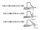
図4は、交流入力電圧が切り換えられた場合のスイッチング素子Q1のソースドレイン電圧Vdsを示す。ここで、図中の上側のグラフは、交流入力電圧が切り換えられていない場合(一例として100V系の定格電圧が入力されている場合)のソースドレイン電圧Vdsと遅延時間との関係を示す。図中の中央のグラフは、交流入力電圧が高くなった場合(一例として200V系の定格電圧に切り換えられた場合)のソースドレイン電圧Vdsと遅延時間との関係を示す。図中の下側のグラフは、交流入力電圧が低くなった場合のソースドレイン電圧Vdsと遅延時間との関係を示す。 FIG. 4 shows the source-drain voltage Vds of the switching element Q1 when the AC input voltage is switched. Here, the upper graph in the figure shows the relationship between the source-drain voltage Vds and the delay time when the AC input voltage is not switched (for example, when a rated voltage of 100 V system is input). The central graph in the figure shows the relationship between the source-drain voltage Vds and the delay time when the AC input voltage is increased (for example, when switched to the rated voltage of 200V system). The lower graph in the figure shows the relationship between the source-drain voltage Vds and the delay time when the AC input voltage becomes low.
図中に太線の破線で示されるように、交流入力電圧が切り換えられた場合には、遅延時間が調整されないと、スイッチング素子Q1のソースドレイン電圧Vdsが極小ではないタイミングがターンオンタイミングとなってしまい、スイッチング損失が大きくなってしまう。これに対し、本実施形態に係る電源制御装置6ではスイッチング素子Q1のオン期間中におけるインダクタ電圧に基づく補助巻線電圧VZCDに応じて遅延時間が調整される結果、スイッチング素子Q1のソースドレイン電圧Vdsが極小となるタイミングにターンオンタイミングが揃うため、スイッチング損失を低減することができる。
As indicated by the thick dashed line in the figure, when the AC input voltage is switched, unless the delay time is adjusted, the timing at which the source-drain voltage Vds of the switching element Q1 is not minimal becomes the turn-on timing. , the switching loss increases. On the other hand, in the power
[3.遅延調整部64]
図5は、遅延調整部64を示す。本実施形態において遅延調整部64は、スイッチング素子Q1のオン期間中においてインダクタ電圧に基づく電流IZCDが基準値以上となったと判定した場合に、電流IZCDが基準値以上とならなかった場合よりも遅延時間を小さくする。また、遅延調整部64は、スイッチング素子Q1のオン期間中における電流IZCDに基づいて、複数種類の定格電圧(本実施形態では一例として100V系および200V系の2種類)のそれぞれに応じた遅延時間設定値のうちいずれを遅延時間として用いるかを切り替える。遅延調整部64は、入力電圧識別部7および遅延回路8を有する。
[3. Delay adjustment unit 64]
FIG. 5 shows the
[3-1.入力電圧識別部7]
入力電圧識別部7は、電流IZCDに基づいて昇圧チョッパ4への入力電圧が複数種類の定格電圧の何れであるかを識別するものである。例えば入力電圧識別部7は、スイッチング素子Q1のオン期間中に電流IZCDが基準値以上になったか否かにより入力電圧が2種類の定格電圧の何れであるかを識別する。入力電圧識別部7は、カレントミラー回路70と、NPN型のバイポーラトランジスタ71と、抵抗72と、コンパレータ73と、ホールド回路74とを有する。
[3-1. Input voltage identification unit 7]
The input
カレントミラー回路70は、入力側のトランジスタ701の出力電流Icに応じた電流Iin_detを、出力側のトランジスタ702から出力する。ここで、電流Icと、電流Iin_detとの電流比はN:1であってよい。
The
NPN型のバイポーラトランジスタ71は、トランジスタ701とゼロクロス検出端子ZCDとの間に接続され、トランジスタ701の側にコレクタ端子、ゼロクロス検出端子ZCDの側にエミッタ端子が配置されている。バイポーラトランジスタ71のベース端子には固定値のベース電流Ibが入力されている。
The NPN-type
ここで、スイッチング素子Q1がオン状態の場合には、ゼロクロス検出端子ZCDから補助巻線L2の側に向かい、インダクタ電圧に応じた引き込み電流IZCDが流れる結果、バイポーラトランジスタ71からゼロクロス検出端子ZCDに向かって同量の電流が流れる。つまり、IZCD=Ic+Ibとなる。これにより、スイッチング素子Q1がオン状態の場合には、カレントミラー回路70の出力側の電流はIin_det=Ic/N=(IZCD-Ib)/Nとなる。
Here, when the switching element Q1 is in the ON state, a pull-in current IZCD corresponding to the inductor voltage flows from the zero-cross detection terminal ZCD toward the auxiliary winding L2. The same amount of current flows in both directions. That is, I ZCD =Ic+Ib. As a result, when the switching element Q1 is on, the current on the output side of the
抵抗72は、電流Iin_detに応じた電圧(検出電圧Vin_detとも称する)を検出するものであり、カレントミラー回路70のトランジスタ702と、接地との間に接続されている。
A
コンパレータ73は、昇圧チョッパ4への入力電圧が2種類の定格電圧の何れであるかを識別するものである。コンパレータ73の非反転入力端子にはトランジスタ702および抵抗72の接続点が接続されて検出電圧Vin_det(=Iin_det×R72)(但しR72は抵抗72の抵抗値)が入力され、反転入力端子には基準電圧Vthが入力される。基準電圧Vthは、入力電圧が100V系であるか、200V系であるかを識別するための電圧であり、例えば、入力電圧が100Vの場合の検出電圧Vin_detと、入力電圧が200Vの場合の検出電圧Vin_detとの間の電圧であってよい。
The
これにより、スイッチング素子Q1がオン状態の場合におけるコンパレータ73の出力信号は、入力電圧が100V系である場合にローレベルとなり、入力電圧が200V系である場合にハイレベルとなる。なお、スイッチング素子Q1がオフ状態の場合には電流IZCDや電流Ic、電流Iin_detなどが小さくなって検出電圧Vin_detが低下するため、コンパレータ73の出力信号はローレベルとなってよい。コンパレータ73は、出力信号をホールド回路74に供給する。
As a result, when the switching element Q1 is in the ON state, the output signal of the
ホールド回路74は、スイッチング素子Q1がオン状態のときのコンパレータ73の出力信号をホールドする。ホールド回路74には、図示しないクロック回路からクロック信号CLKが入力される。クロック信号CLKの周期は交流電源2の1周期や半周期に設定されてよく、一例として20ms,10msなどであってよい。なお、クロック回路は、スイッチング素子Q1がオン状態のときのコンパレータ73の出力信号をホールドするように、RS型フリップフロップ655からの出力信号QQの入力端子を有してよい。これにより、クロック回路は、スイッチング素子Q1がオン状態となるタイミング、すなわち、出力信号QQのオンタイミングに若干の遅延を持たせたタイミングでクロック信号CLKを所定周期で出力するように構成してよい。ホールド回路74は、遅延回路741と、RS型フリップフロップ742と、D型フリップフロップ743とを有する。
The
遅延回路741は、D型フリップフロップ743の取り込みタイミングよりも、RS型フリップフロップ742のリセットタイミングを遅らせる。遅延回路741は、クロック信号CLKを遅延させてRS型フリップフロップ742に供給してよい。
The
RS型フリップフロップ742は、セット端子にコンパレータ73の出力信号が入力され、リセット端子に遅延回路741を介して遅延されたクロック信号が入力される。RS型フリップフロップ742は出力端子からの出力信号をD型フリップフロップ743に供給する。
The RS-type flip-
D型フリップフロップ743は、入力端子にRS型フリップフロップ742の出力端子が接続される。D型フリップフロップ743は、クロック信号CLKのクロックタイミングに同期してRS型フリップフロップ742の出力信号の値を取り込んで保持し、保持する値に対応する出力信号Vin_det_onを出力する。D型フリップフロップ743は、出力信号Vin_det_onを遅延回路8およびターンオンタイマ部9に供給する。
The input terminal of the D-type flip-
以上のホールド回路74によれば、スイッチング素子Q1がオン状態のときに入力電圧が200V系になると、スイッチング素子Q1のオン期間にRS型フリップフロップ742がセットされてハイレベルの信号がD型フリップフロップ743により保持されて出力信号Vin_det_onとして出力される。一方、入力電圧が100V系のままであると、スイッチング素子Q1のオン期間にRS型フリップフロップ742がセットされずにローレベルの信号がD型フリップフロップ743により保持されて出力信号Vin_det_onとして出力される。D型フリップフロップ743の保持信号はクロック信号CLKの周期ごとに更新され、RS型フリップフロップ742は遅延回路741で遅延されたクロック信号CLKによりD型フリップフロップ743の更新後にリセットされる。
According to the
ここで、ホールド回路74の出力信号Vin_det_onはスイッチング素子Q1のオン期間における電流IZCDに基づくものであり、遅延回路8に供給されて、次にスイッチング素子Q1をターンオンするための遅延時間の調整に用いられる。これにより、次にスイッチング素子Q1をターンオンするための遅延時間の調整は、スイッチング素子Q1のスイッチング周期の直前のオン期間における電流IZCDに基づいて行ってもよい。この場合、クロック回路は、クロック信号CLKの周期を交流電源2の1周期や半周期ではなく、出力信号QQのオンタイミングに若干の遅延を持たせたタイミングとしてよい。
Here, the output signal V in_det_on of the
[3-2.遅延回路8]
遅延回路8は、検出部63からの検出信号VZCD<thがハイレベルとなってから、予め設定された遅延時間後にハイレベルとなる信号SDLYを出力するとともに、入力電圧識別部7による識別結果に応じて遅延時間を調整する。遅延回路8は、100V系,200V系の定格電圧に対応する2つの遅延時間設定値のうち、何れの遅延時間設定値を遅延時間として用いるかを電圧識別信号Vin_detに応じて切り替えてよい。遅延回路8は、ノットゲート80,81と、電流源82と、NチャネルMOSFET83と、コンデンサ部85と、コンパレータ86とを有する。
[3-2. delay circuit 8]
The
ノットゲート80は、検出部63と、NチャネルMOSFET83のゲート端子との間に接続され、検出部63からの検出信号VZCD<thを反転してNチャネルMOSFET83のゲート端子に供給する。ノットゲート81は、入力電圧識別部7と、コンデンサ部85との間に接続され、入力電圧識別部7からの出力信号Vin_det_onを反転してコンデンサ部85に供給する。
The not
電流源82は、コンデンサ部85と直列に接続され、定電流をコンデンサ部85に供給してコンデンサ部85を充電する。
The current source 82 is connected in series with the
NチャネルMOSFET83は、電流源82と接地との間で、コンデンサ部85と並列に接続される。NチャネルMOSFET83は、ノットゲート80から供給される検出信号VZCD<thの反転信号によりゲート駆動される。NチャネルMOSFET83は、オフ状態では電流源82からの電流をコンデンサ部85に流してコンデンサ部85を充電させ、オン状態では電流源82からの電流を流すとともにコンデンサ部85を放電する。
N-
コンデンサ部85は、NチャネルMOSFET83がオフ状態の場合に充電され、充電量に応じた充電電圧VDLY85を発生する。また、コンデンサ部85は、スイッチング素子Q1のオン期間中における電流IZCDに基づいて容量を切り替えることにより、2種類の遅延時間設定値のうちいずれを遅延時間として用いるかを切り替える。コンデンサ部85は、コンデンサ851と、コンデンサ851に対して並列に接続されたNチャネルMOSFET852およびコンデンサ853の直列回路とを有する。
コンデンサ851は、電流源82および接地の間に接続されており、電流源82からの電流により充電される。NチャネルMOSFET852は、コンデンサ853と接地との間に接続され、ノットゲート81から供給される出力信号Vin_det_onの反転信号によりゲート駆動される。つまり、NチャネルMOSFET852は、電流IZCDが基準値以上とならなかった場合(本実施形態では一例として検出電圧Vin_detが基準電圧Vth以上とならなかった場合)にオン状態とされ、電流IZCDが基準値以上となった場合にオフ状態とされる。コンデンサ853は、電流源82と接地との間でNチャネルMOSFET852と直列に接続されており、NチャネルMOSFET852がオン状態の場合に電流源82からの電流により充電され、NチャネルMOSFET852がオフ状態の場合には充電されない。
これにより、電流IZCDが基準値以上とならなかった場合にはコンデンサ部85の容量が大きくなり、電流IZCDが基準値以上となった場合にはコンデンサ部85の容量が小さくなる。なお、NチャネルMOSFET852はコンデンサ853に対して電流源82の側に接続されてもよい。
As a result, the capacitance of
コンパレータ86は、非反転入力端子に充電電圧VDLY85が入力され、反転入力端子に基準電圧Vref86が入力される。ここで、コンデンサ部85は検出部63からの検出信号VZCD<thがハイレベルとなることに応じて充電され始め、コンデンサ部85の充電が開始してから充電電圧VDLY85が基準電圧Vref86に達すると、出力信号SDLYがハイレベルとなりスイッチング素子Q1がターンオンされる。そのため、コンデンサ部85の充電開始から充電電圧VDLY85が基準電圧Vref86に達するまでの経過時間はスイッチング素子Q1をターンオンするための遅延時間となる。そして、上述したように電流IZCDが基準値以上とならなかった場合にはコンデンサ部85の容量が大きくなるため、充電電圧VDLY85の増加速度が小さくなって遅延時間は大きくなる。また、電流IZCDが基準値以上となった場合にはコンデンサ部85の容量が小さくなるため、充電電圧VDLY85の増加速度が大きくなって遅延時間は小さくなる。
The
なお、基準電圧Vref86は、入力電圧が100V系および200V系であるそれぞれの場合に、検出信号VZCD<thがハイレベルとなるタイミング(tVZCD=th)からインダクタ電流IL1がゼロになりソースドレイン電圧Vdsが極小になるタイミング(tVds=min)までの経過時間でコンデンサ部85に充電を行わせた場合の充電電圧VDLY85に設定されてよい。これにより、インダクタ電流IL1がゼロになりソースドレイン電圧Vdsが極小になるタイミング(tVds=min)でコンパレータ86の出力信号SDLYがハイレベルになり、スイッチング素子Q1がターンオンされる。
Note that the reference voltage V ref 86 is such that the inductor current I L1 becomes zero from the timing (t VZCD=th ) when the detection signal V ZCD<th becomes high level when the input voltage is of the 100 V system or the 200 V system. It may be set to the charging voltage V DLY85 when the
以上の遅延調整部64によれば、オン期間中の電流IZCDが基準値以上となった場合に、ならなかった場合よりも遅延時間を小さくするので、入力電圧が大きい場合に遅延時間が小さくなる。従って、インダクタL1とスイッチング素子Q1の入力容量(CISS)とを有する疑似共振回路の共振によってスイッチング素子Q1のソースドレイン電圧Vdsがターンオフ後に減少から増加に転じる前に、スイッチング素子Q1をターンオンすることができる。よって、ソースドレイン電圧Vdsが確実に極小になるタイミングでスイッチング素子Q1のターンオンを行い、ターンオンによるスイッチング損失を確実に低減することができる。
According to the
また、スイッチング素子Q1のオン期間中における電流IZCDに基づいて、複数種類の定格電圧のそれぞれに応じた遅延時間設定値のうちいずれを用いるかを切り替える。従って、交流電源2が切り換えられる場合であっても、インダクタ電流IL1がゼロになりソースドレイン電圧Vdsが極小になるタイミング(tVds=min)でスイッチング素子Q1をターンオンすることができる。 Further, based on the current IZCD during the ON period of the switching element Q1, it is switched which one of the delay time setting values to be used according to each of the plurality of types of rated voltages. Therefore, even when the AC power supply 2 is switched, the switching element Q1 can be turned on at the timing (t Vds=min ) when the inductor current IL1 becomes zero and the source-drain voltage Vds becomes minimum.
[4.ターンオンタイマ部9]
図6は、ターンオンタイマ部9を示す。ターンオンタイマ部9は、予め設定された時間内にスイッチング素子Q1がオフ状態からターンオンされない場合にハイレベルとなる信号Stimerを出力する。ターンオンタイマ部9は、スイッチング素子Q1のオフ期間の開始から予め定められたターンオンタイマ時間の後にスイッチング素子Q1をターンオンしてよい。これにより、例えば、スイッチング素子Q1のオフ期間中において補助巻線電圧VZCDがゼロクロス基準電圧Vth_zcd以上からゼロクロス基準電圧Vth_zcd未満に変化した回数がボトムスキップ制御の基準回数に達しない場合においても、スイッチング素子Q1がターンオンされる。なお、本実施形態では一例としてターンオンタイマ時間の開始タイミングをスイッチング素子Q1がターンオフされるタイミングとして説明するが、補助巻線電圧VZCDが最初にゼロクロス基準電圧Vth_zcd以上からゼロクロス基準電圧Vth_zcd未満に変化したタイミングであってもよい。ターンオンタイマ時間はスイッチング素子Q1のオン期間中における電流IZCDに基づいて遅延調整部64により調整されてよい。一例として、ターンオンタイマ部9は、100V系,200V系の定格電圧に対応する2つのターンオンタイマ時間の設定値のうち、何れの設定値をターンオンタイマ時間として用いるかを遅延調整部64からの電圧識別信号Vin_detに応じて切り替えてよい。ターンオンタイマ部9は、電流源92と、NチャネルMOSFET93と、ノットゲート94と、コンデンサ部95と、コンパレータ96とを有する。
[4. turn-on timer unit 9]
FIG. 6 shows the turn-on
電流源92は、コンデンサ部95と直列に接続され、定電流をコンデンサ部95に供給してコンデンサ部95を充電する。
The
NチャネルMOSFET93は、電流源92と接地との間で、コンデンサ部95と並列に接続される。NチャネルMOSFET93は、スイッチ制御部65のRS型フリップフロップ655からの出力信号QQによりゲート駆動される。これにより、出力信号QQがローレベルの状態、つまりスイッチング素子Q1がオフ状態の場合には、NチャネルMOSFET93もオフ状態となり、電流源92からの電流をコンデンサ部95に流してコンデンサ部95を充電させる。出力信号QQがハイレベルの状態、つまりスイッチング素子Q1がオン状態の場合には、NチャネルMOSFET93もオン状態となり、電流源92からの電流を流すとともにコンデンサ部95を放電する。
N-
ノットゲート94は、入力電圧識別部7と、コンデンサ部95との間に接続され、入力電圧識別部7からの出力信号Vin_det_onを反転してコンデンサ部95に供給する。
The not
コンデンサ部95は、NチャネルMOSFET93がオフ状態の場合に充電され、充電量に応じた充電電圧VDLY95を発生する。また、コンデンサ部95は、スイッチング素子Q1のオン期間中における電流IZCDに基づいて容量を切り替えることにより、2種類のターンオンタイマ時間の設定値のうちいずれをターンオンタイマ時間として用いるかを切り替える。コンデンサ部95は、コンデンサ951と、コンデンサ951に対して並列に接続されたNチャネルMOSFET952およびコンデンサ953の直列回路とを有する。
コンデンサ951は、電流源92および接地の間に接続されており、電流源92からの電流により充電される。NチャネルMOSFET952は、コンデンサ953と接地との間に接続され、ノットゲート94から供給される出力信号Vin_det_onの反転信号によりゲート駆動される。つまり、NチャネルMOSFET952は、電流IZCDが基準値以上とならなかった場合(本実施形態では一例として検出電圧Vin_detが基準電圧Vth以上とならなかった場合)にオン状態とされ、電流IZCDが基準値以上となった場合にオフ状態とされる。コンデンサ953は、電流源92と接地との間でNチャネルMOSFET952と直列に接続されており、NチャネルMOSFET952がオン状態の場合に電流源92からの電流により充電され、NチャネルMOSFET952がオフ状態の場合には充電されない。
これにより、電流IZCDが基準値以上とならなかった場合にはコンデンサ部95の容量が大きくなり、電流IZCDが基準値以上となった場合にはコンデンサ部95の容量が小さくなる。なお、NチャネルMOSFET952はコンデンサ953に対して電流源92の側に接続されてもよい。
As a result, the capacitance of
コンパレータ96は、非反転入力端子に充電電圧VDLY95が入力され、反転入力端子に基準電圧Vref96が入力される。ここで、コンデンサ部95の充電が開始してから充電電圧VDLY95が基準電圧Vref96に達すると、出力信号Stimerがハイレベルとなりスイッチング素子Q1がターンオンされる。そのため、コンデンサ部95の充電開始から充電電圧VDLY95が基準電圧Vref96に達するまでの経過時間はターンオンタイマ時間となる。そして、上述したように電流IZCDが基準値以上とならなかった場合にはコンデンサ部95の容量が大きくなるため、充電電圧VDLY95の増加速度が小さくなって遅延時間は大きくなる。また、電流IZCDが基準値以上となった場合にはコンデンサ部95の容量が小さくなるため、充電電圧VDLY95の増加速度が大きくなって遅延時間は小さくなる。
A
なお、基準電圧Vref96は、入力電圧が100V系および200V系であるそれぞれの場合に、スイッチング素子Q1がターンオフされてからインダクタ電流IL1がボトムスキップ制御における基準回数(本実施形態では2回)だけゼロになりスイッチング素子Q1のソースドレイン電圧Vdsが極小となるまでの経過時間でコンデンサ部95に充電を行わせた場合の充電電圧VDLY95に設定されてよい。これにより、補助巻線電圧VZCDがゼロクロス基準電圧Vth_zcd未満に変化した回数が2回に達せずに遅延回路8からハイレベルの信号SDLYが出力されない場合であっても、インダクタ電流IL1がゼロになりソースドレイン電圧Vdsが極小になるタイミング(tVds=min)でコンパレータ96の出力信号Stimerがハイレベルになり、スイッチング素子Q1がターンオンされる。
Note that the reference voltage V ref 96 is such that when the input voltage is of the 100 V system and the 200 V system, the inductor current I L1 is the reference number of times (twice in this embodiment) in the bottom skip control after the switching element Q1 is turned off. may be set to the charging voltage V DLY95 when the
以上のターンオンタイマ部9によれば、補助巻線電圧VZCDがゼロクロス基準電圧Vth_zcd以上からゼロクロス基準電圧Vth_zcd未満に変化した回数がボトムスキップ制御における基準回数に達しない場合においても、インダクタ電流IL1がゼロになりスイッチング素子Q1のソースドレイン電圧Vdsが極小になるタイミング(tVds=min)でスイッチング素子Q1を確実にターンオンすることができる。
According to the turn-on
[5.動作]
図7は、電源制御装置6の一部の動作を示す。電源制御装置6は、ステップS11~S15の処理を行うことにより、スイッチング損失を低減してエネルギー効率を向上させる。
[5. motion]
FIG. 7 shows the operation of part of the
ステップS11において、スイッチ制御部65は、昇圧チョッパ4のスイッチング素子Q1のオンオフを制御する。例えば、スイッチ制御部65は、遅延調整部64からの出力信号SDLYと、ターンオンタイマ部9からの出力信号Stimerとの少なくとも一方がハイレベルとなることに応じてスイッチング素子Q1をターンオンする。また、スイッチ制御部65は、ランプ波Rampが誤差信号VCOMPよりも大きくなる期間にスイッチング素子Q1がオフとなるようスイッチング素子Q1を制御する。
In step S<b>11 , the
ステップS13において、検出部63は、昇圧チョッパ4の補助巻線電圧VZCDがゼロクロス基準電圧Vth_zcd未満となったことを検出する。検出部63は、ボトムスキップ制御における基準回数だけ補助巻線電圧VZCDがゼロクロス基準電圧Vth_zcd未満となったことを検出し、検出信号VZCD<thをハイレベルとしてよい。
In step S13, the
ステップS15において、遅延調整部64は、スイッチング素子Q1のオフ期間中に補助巻線電圧VZCDがゼロクロス基準電圧Vth_zcd未満となったことが検出されてから、ステップS11の処理においてスイッチング素子Q1をターンオンするまでの遅延時間を、スイッチング素子Q1のオン期間中における電流IZCDに応じて調整する。本実施形態では、遅延調整部64は、検出信号VZCD<thがハイレベルとなってからスイッチング素子Q1をターンオンするまでの遅延時間を電流IZCDに基づき切り替えてよい。また、遅延調整部64は、電流IZCDに基づいて、100V系および200V系の定格電圧に応じた遅延時間設定値のうちいずれを遅延時間として用いるかを切り替えてよい。これにより、電流IZCDに応じて遅延時間が調整され、調整後の遅延時間に応じたタイミングで遅延調整部64からの出力信号SDLYがハイレベルとなる。
In step S15, the
また、遅延調整部64は、スイッチング素子Q1のオン期間中における電流IZCDに基づいて、ターンオンタイマ時間を更に調整する。これにより、電流IZCDに応じてターンオンタイマ時間が調整され、スイッチング素子Q1のオフ期間中において補助巻線電圧VZCDがゼロクロス基準電圧Vth_zcd以上からゼロクロス基準電圧Vth_zcd未満に変化した回数がボトムスキップ制御の基準回数に達しない場合においても、ターンオンタイマ部9からの出力信号Stimerがハイレベルとなる。
以降、電源制御装置6はステップS11~S15の処理を繰り返す。
Further, the
After that, the
[6.変形例]
図8は、変形例に係る入力電圧識別部7Aを示す。入力電圧識別部7Aは、抵抗75と、トランスコンダクタンスアンプ76とをさらに有する。抵抗75は、バイポーラトランジスタ71のベース端子に接続されベース電流Ibを電圧に変換する。トランスコンダクタンスアンプ76は、抵抗75の両端に非反転入力端子および反転入力端子が接続されており、抵抗75の両端に生じる電圧にトランスコンダクタンス(gm)を乗じた電流(=Ib×R75×gm)(但し、R75は抵抗75の抵抗値)をトランジスタ702および抵抗72の接続点に出力する。
[6. Modification]
FIG. 8 shows an input
以上の入力電圧識別部7Aによれば、抵抗72によって検出されてコンパレータ73の非反転入力端子に入力される検出電圧はVin_det=(Iin_det+Ib×R75×gm)×R72となる。従って、図4に示した入力電圧識別部7と異なり、ベース電流Ibも考慮に入れて入力電圧の識別を行うことができるため、入力電圧を正確に識別することができる。なお、抵抗75の抵抗値R75、トランスコンダクタンスアンプ76のトランスコンダクタンス(gm)、および、カレントミラー回路70の電流比Nは、R75×gm=1/Nを満たすように設定されてよい。この場合には、検出電圧Vin_det=IZCD×R72/Nとなる。
According to the input
図9は、他の変形例に係る入力電圧識別部7Bを示す。入力電圧識別部7Bは、カレントミラー回路77をさらに有する。カレントミラー回路77は、入力側のトランジスタ771がバイポーラトランジスタ71のベース端子に接続され、出力側のトランジスタ772がトランジスタ702および抵抗72の接続点に接続される。カレントミラー回路77における入力側および出力側の電流比はN:1であってよい。
FIG. 9 shows an input
以上の入力電圧識別部7Bによれば、抵抗72によって検出されてコンパレータ73の非反転入力端子に入力される検出電圧はVin_det=(Ic/N+Ib/N)×R72=IZCD×R72/Nとなる。従って、図4に示した入力電圧識別部7と異なり、ベース電流Ibも考慮に入れて入力電圧の識別を行うことができるため、入力電圧を正確に識別することができる。
According to the input
[7.その他の変形例]
上記の実施形態においては、インダクタL1に対し補助巻線L2が逆極性に巻線され、入力電圧識別部7は、スイッチング素子Q1のスイッチングオン期間に主巻線L1に現れる入力電圧にNs/Npを乗じた補助巻線電圧VZCDを電流IZCDから間接的に検出した。具体的には、電源制御装置6から流れ出る電流IZCDを電圧に変換し、交流入力電圧を識別した。しかし、スイッチング素子Q1のスイッチングオフ期間には、入出力電圧差に巻数比(Ns/Np)倍した電圧が補助巻線L2に現れるので、この電圧に基づき電源制御装置6に流れ込む電流を電圧に変換し、交流入力電圧を識別してもよい。すなわち、入力電圧識別部7は、スイッチング素子Q1のスイッチングオフ期間に電源制御装置6に流れ込む電流を電圧に変換して交流入力電圧を識別してよい。この場合、遅延調整部64は、遅延時間を、スイッチング素子Q1のオフ期間中におけるインダクタ電圧に基づく第2の値(電源制御装置6に流れ込む電流)に応じて調整してよいし、この第2の値に基づいてターンオンタイマ時間を更に調整してよい。
[7. Other Modifications]
In the above-described embodiment, the auxiliary winding L2 is wound with the polarity opposite to that of the inductor L1, and the input
また、交流電源2および全波整流回路3が電源装置1に具備されることとして説明したが、これらの少なくとも一方は電源装置1に具備されずに電源装置1に外部接続されてもよい。
Also, although the AC power supply 2 and the full-
また、電源制御装置6は比較電圧生成部61およびプラス電圧クランプ回路62を有することとして説明したが、これらの少なくとも1つを有しないこととしてもよい。
Also, although the power
また、電源制御装置6は交流入力電圧が複数種類の定格電圧の何れであるかを識別して遅延時間を調整することとして説明したが、交流入力電圧の変動に伴ってスイッチング素子Q1のオン期間中における電流IZCDが変化したことに応じて、遅延時間を調整してもよい。例えば、電源制御装置6は、一の定格電圧の範囲内での交流入力電圧の変動を電流IZCDの変化により検出して遅延時間を調整してよい。一例として、電源制御装置6は、交流電源2が100V系の定格電圧である場合に、交流入力電圧が100V未満、100V~105V、105V~110V、110V以上の何れであるかを検出して遅延時間を調整してよい。この場合には、交流入力電圧が許容範囲内で変動する場合に、インダクタ電流IL1がゼロになりスイッチング素子Q1のソースドレイン電圧Vdsが極小になるタイミングでスイッチング素子Q1をターンオンすることができる。
In addition, although the power
また、遅延回路8はコンデンサ部85内で充電可能なコンデンサの数を切り替えることで遅延時間を調整することとして説明したが、コンパレータ86の基準電圧Vref86を切り替えることで遅延時間を調整してもよい。同様に、ターンオンタイマ部9はコンデンサ部95内で充電可能なコンデンサの数を切り替えることでターンオンタイマ時間を調整することとして説明したが、コンパレータ96の基準電圧Vref96を切り替えることでターンオンタイマ時間を調整してもよい。
Further, the
また、電源制御装置6はボトムスキップ制御を行うこととして説明したが、行わなくてもよい。この場合には、検出部63は、補助巻線電圧VZCDがゼロクロス基準電圧Vth_zcd未満となったことに応じてハイレベルとなる検出信号VZCD<thを出力してよい。
Also, although the power
また、インダクタ電圧に基づく第1の値を補助巻線電圧VZCDとし、インダクタ電圧に基づく第2の値を電流IZCDとして説明したが、インダクタ電圧そのものとしてもよいし、インダクタ電圧に基づく他の値としてもよい。例えば、第1の値を電流IZCDとし、第2の値を補助巻線電圧VZCDとしてもよい。また、第1の値および第2の値は同じ値であってもよい。 Also, although the first value based on the inductor voltage is assumed to be the auxiliary winding voltage VZCD and the second value based on the inductor voltage is assumed to be the current IZCD , the inductor voltage itself may be used, or another value based on the inductor voltage may be used. value. For example, the first value may be the current I ZCD and the second value may be the auxiliary winding voltage V ZCD . Also, the first value and the second value may be the same value.
以上、本発明を実施の形態を用いて説明したが、本発明の技術的範囲は上記実施の形態に記載の範囲には限定されない。上記実施の形態に、多様な変更または改良を加えることが可能であることが当業者に明らかである。その様な変更または改良を加えた形態も本発明の技術的範囲に含まれ得ることが、特許請求の範囲の記載から明らかである。 Although the present invention has been described above using the embodiments, the technical scope of the present invention is not limited to the scope described in the above embodiments. It is obvious to those skilled in the art that various modifications and improvements can be made to the above embodiments. It is clear from the description of the scope of claims that forms with such modifications or improvements can also be included in the technical scope of the present invention.
特許請求の範囲、明細書、および図面中において示した装置、システム、プログラム、および方法における動作、手順、ステップ、および段階等の各処理の実行順序は、特段「より前に」、「先立って」等と明示しておらず、また、前の処理の出力を後の処理で用いるのでない限り、任意の順序で実現しうることに留意すべきである。特許請求の範囲、明細書、および図面中の動作フローに関して、便宜上「まず、」、「次に、」等を用いて説明したとしても、この順で実施することが必須であることを意味するものではない。 The execution order of each process such as actions, procedures, steps, and stages in the devices, systems, programs, and methods shown in the claims, the specification, and the drawings is particularly "before", "before etc., and it should be noted that they can be implemented in any order unless the output of the previous process is used in the subsequent process. Regarding the operation flow in the claims, the specification, and the drawings, even if the description is made using "first," "next," etc. for the sake of convenience, it means that it is essential to carry out in this order. not a thing
1 電源装置、2 交流電源、3 全波整流回路、4 昇圧チョッパ、5 電圧誤差検出補償回路、6 電源制御装置、7 入力電圧識別部、7A 入力電圧識別部、7B 入力電圧識別部、8 遅延回路、9 ターンオンタイマ部、50 RC位相補償回路、C50 コンデンサ、R50 抵抗、C51 コンデンサ、61 比較電圧生成部、61a エラーアンプ、62 プラス電圧クランプ回路、62a ツェナーダイオード、63 検出部、64 遅延調整部、65 スイッチ制御部、70 カレントミラー回路、71 バイポーラトランジスタ、72 抵抗、73 コンパレータ、74 ホールド回路、75 抵抗、76 トランスコンダクタンスアンプ、77 カレントミラー回路、80 ノットゲート、81 ノットゲート、82 電流源、83 NチャネルMOSFET、85 コンデンサ部、86 コンパレータ、92 電流源、93 NチャネルMOSFET、94 ノットゲート、95 コンデンサ部、96 コンパレータ、652 オアゲート、653 発振器、654 パルス幅変調用コンパレータ、655 RS型フリップフロップ、701 トランジスタ、702 トランジスタ、741 遅延回路、742 RS型フリップフロップ、743 D型フリップフロップ、771 トランジスタ、772 トランジスタ、851 コンデンサ、852 NチャネルMOSFET、853 コンデンサ、951 コンデンサ、952 NチャネルMOSFET、953 コンデンサ、C1 出力コンデンサ、D1 ダイオード、L1 インダクタ、L2 補助巻線、Q1 スイッチング素子、R1 分圧抵抗、R2 分圧抵抗、R4 検出抵抗、T トランス 1 power supply device 2 AC power supply 3 full-wave rectifier circuit 4 step-up chopper 5 voltage error detection compensation circuit 6 power control device 7 input voltage identification unit 7A input voltage identification unit 7B input voltage identification unit 8 delay Circuit, 9 turn-on timer section, 50 RC phase compensation circuit, C50 capacitor, R50 resistor, C51 capacitor, 61 comparison voltage generation section, 61a error amplifier, 62 plus voltage clamp circuit, 62a Zener diode, 63 detection section, 64 delay adjustment section , 65 switch control unit, 70 current mirror circuit, 71 bipolar transistor, 72 resistor, 73 comparator, 74 hold circuit, 75 resistor, 76 transconductance amplifier, 77 current mirror circuit, 80 not gate, 81 not gate, 82 current source, 83 N-channel MOSFET, 85 Capacitor section, 86 Comparator, 92 Current source, 93 N-channel MOSFET, 94 Not gate, 95 Capacitor section, 96 Comparator, 652 OR gate, 653 Oscillator, 654 Pulse width modulation comparator, 655 RS type flip-flop , 701 transistor, 702 transistor, 741 delay circuit, 742 RS-type flip-flop, 743 D-type flip-flop, 771 transistor, 772 transistor, 851 capacitor, 852 N-channel MOSFET, 853 capacitor, 951 capacitor, 952 N-channel MOSFET, 953 capacitor , C1 output capacitor, D1 diode, L1 inductor, L2 auxiliary winding, Q1 switching element, R1 voltage dividing resistor, R2 voltage dividing resistor, R4 detection resistor, T transformer
Claims (9)
前記昇圧チョッパのインダクタのインダクタ電圧に基づく第1の値が閾値未満となったことを検出する検出部と、
前記検出部によって前記第1の値が前記閾値未満となったことが検出されてから、前記スイッチ制御部が前記スイッチング素子をターンオンするまでの遅延時間を、前記スイッチング素子のオン期間中での前記インダクタ電圧に基づく第2の値に応じて調整する遅延調整部と
を備える電源制御装置。 a switch control unit that controls on/off of the switching element of the boost chopper;
a detection unit that detects that a first value based on the inductor voltage of the inductor of the boost chopper is less than a threshold;
The delay time from when the detection unit detects that the first value has become less than the threshold value to when the switch control unit turns on the switching element is set to the above- mentioned and a delay adjuster that adjusts according to a second value based on the inductor voltage.
前記昇圧チョッパのインダクタのインダクタ電圧に基づく第1の値が閾値未満となったことを検出する検出部と、
前記検出部によって前記第1の値が前記閾値未満となったことが検出されてから、前記スイッチ制御部が前記スイッチング素子をターンオンするまでの遅延時間を、前記インダクタ電圧に基づく第2の値に応じて調整する遅延調整部と
を備え、
前記遅延調整部は、
前記第2の値が基準値以上となったと判定した場合に、前記第2の値が前記基準値以上とならなかった場合よりも前記遅延時間を小さくする電源制御装置。 a switch control unit that controls on/off of the switching element of the boost chopper;
a detection unit that detects that a first value based on the inductor voltage of the inductor of the boost chopper is less than a threshold;
A delay time from when the detection unit detects that the first value has become less than the threshold value to when the switch control unit turns on the switching element is set to a second value based on the inductor voltage. and a delay adjustment unit that adjusts according to
The delay adjustment unit
A power supply control device that reduces the delay time when it is determined that the second value is equal to or greater than a reference value than when the second value is not equal to or greater than the reference value .
前記スイッチング素子のオン期間中において前記第2の値が基準値以上となったか否かを判定する
請求項1または2に記載の電源制御装置。 The delay adjustment unit
3. The power supply control device according to claim 1, wherein it is determined whether or not said second value is greater than or equal to a reference value during an ON period of said switching element.
前記昇圧チョッパのインダクタのインダクタ電圧に基づく第1の値が閾値未満となったことを検出する検出部と、
前記検出部によって前記第1の値が前記閾値未満となったことが検出されてから、前記スイッチ制御部が前記スイッチング素子をターンオンするまでの遅延時間を、前記インダクタ電圧に基づく第2の値に応じて調整する遅延調整部と、
前記昇圧チョッパは、前記インダクタとして機能する主巻線および補助巻線を有するトランスと、
を備え、
前記遅延調整部は、補助巻線電圧に応じた電流を前記第2の値として用いる電源制御装置。 a switch control unit that controls on/off of the switching element of the boost chopper;
a detection unit that detects that a first value based on the inductor voltage of the inductor of the boost chopper is less than a threshold;
A delay time from when the detection unit detects that the first value has become less than the threshold value to when the switch control unit turns on the switching element is set to a second value based on the inductor voltage. a delay adjustment unit that adjusts accordingly ;
The boost chopper includes a transformer having a main winding and an auxiliary winding that function as the inductor;
with
The power control device , wherein the delay adjusting unit uses a current corresponding to the auxiliary winding voltage as the second value .
前記昇圧チョッパのインダクタのインダクタ電圧に基づく第1の値が閾値未満となったことを検出する検出部と、
前記検出部によって前記第1の値が前記閾値未満となったことが検出されてから、前記スイッチ制御部が前記スイッチング素子をターンオンするまでの遅延時間を、前記インダクタ電圧に基づく第2の値に応じて調整する遅延調整部と
を備え、
前記遅延調整部は、前記スイッチング素子のオン期間中における前記第2の値に基づいて、複数種類の定格電圧のそれぞれに応じた遅延時間設定値のうちいずれを前記遅延時間として用いるかを切り替える電源制御装置。 a switch control unit that controls on/off of the switching element of the boost chopper;
a detection unit that detects that a first value based on the inductor voltage of the inductor of the boost chopper is less than a threshold;
A delay time from when the detection unit detects that the first value has become less than the threshold value to when the switch control unit turns on the switching element is set to a second value based on the inductor voltage. and a delay adjustment unit that adjusts according to
The delay adjustment unit switches which of delay time setting values corresponding to each of a plurality of types of rated voltages to be used as the delay time based on the second value during an ON period of the switching element. Control device.
前記遅延調整部は、前記第1の値が前記閾値以上から前記閾値未満に変化した回数が予め定められた回数に達してから、前記スイッチ制御部が前記スイッチング素子をターンオンするまでの遅延時間を調整する
請求項1から5のいずれか一項に記載の電源制御装置。 The switch control unit turns on the switching element in response to the number of times the first value changes from the threshold value or more to less than the threshold value reaches a predetermined number of times,
The delay adjustment unit provides a delay time from when the number of times the first value changes from the threshold value or more to less than the threshold value reaches a predetermined number of times until the switch control unit turns on the switching element. The power control device according to any one of claims 1 to 5, wherein the power control device is adjusted.
前記遅延調整部は、前記第2の値に基づいて、前記ターンオンタイマ時間を更に調整する
請求項6に記載の電源制御装置。 The switch control unit has a turn-on timer unit that turns on the switching element after a predetermined turn-on timer time,
7. The power control device according to claim 6 , wherein the delay adjusting section further adjusts the turn-on timer time based on the second value.
前記検出部は、補助巻線電圧を前記第1の値として用いる請求項1から7のいずれか一項に記載の電源制御装置。 The boost chopper comprises a transformer having a main winding and an auxiliary winding that function as the inductor,
The power control device according to any one of claims 1 to 7 , wherein the detection section uses an auxiliary winding voltage as the first value.
Priority Applications (3)
| Application Number | Priority Date | Filing Date | Title |
|---|---|---|---|
| JP2018208270A JP7211018B2 (en) | 2018-11-05 | 2018-11-05 | power control unit |
| CN201911009415.4A CN111146942A (en) | 2018-11-05 | 2019-10-23 | Power supply control device |
| US16/663,304 US10965209B2 (en) | 2018-11-05 | 2019-10-24 | Power supply controller with delay adjustment |
Applications Claiming Priority (1)
| Application Number | Priority Date | Filing Date | Title |
|---|---|---|---|
| JP2018208270A JP7211018B2 (en) | 2018-11-05 | 2018-11-05 | power control unit |
Publications (2)
| Publication Number | Publication Date |
|---|---|
| JP2020078114A JP2020078114A (en) | 2020-05-21 |
| JP7211018B2 true JP7211018B2 (en) | 2023-01-24 |
Family
ID=70457933
Family Applications (1)
| Application Number | Title | Priority Date | Filing Date |
|---|---|---|---|
| JP2018208270A Active JP7211018B2 (en) | 2018-11-05 | 2018-11-05 | power control unit |
Country Status (3)
| Country | Link |
|---|---|
| US (1) | US10965209B2 (en) |
| JP (1) | JP7211018B2 (en) |
| CN (1) | CN111146942A (en) |
Families Citing this family (2)
| Publication number | Priority date | Publication date | Assignee | Title |
|---|---|---|---|---|
| JP6880865B2 (en) * | 2017-03-16 | 2021-06-02 | 富士電機株式会社 | AC / DC converter control circuit |
| EP3806302B1 (en) * | 2019-10-09 | 2022-01-26 | Tridonic GmbH & Co. KG | Power factor correction circuit |
Citations (2)
| Publication number | Priority date | Publication date | Assignee | Title |
|---|---|---|---|---|
| JP2017077171A (en) | 2014-12-22 | 2017-04-20 | 三菱電機株式会社 | Light source lighting device and lighting fixture |
| JP2017225260A (en) | 2016-06-16 | 2017-12-21 | 富士電機株式会社 | Switching power supply device |
Family Cites Families (10)
| Publication number | Priority date | Publication date | Assignee | Title |
|---|---|---|---|---|
| JPH06165498A (en) * | 1992-11-20 | 1994-06-10 | Matsushita Electric Works Ltd | Power supply device |
| KR960016605B1 (en) * | 1992-11-20 | 1996-12-16 | 마쯔시다 덴꼬 가부시끼가이샤 | Power supply |
| US6977492B2 (en) * | 2002-07-10 | 2005-12-20 | Marvell World Trade Ltd. | Output regulator |
| KR101026248B1 (en) | 2004-09-21 | 2011-03-31 | 페어차일드코리아반도체 주식회사 | Power Factor Correction Circuit |
| JP5302755B2 (en) * | 2009-04-24 | 2013-10-02 | パナソニック株式会社 | Power supply |
| JP5966606B2 (en) * | 2012-05-17 | 2016-08-10 | 富士電機株式会社 | Switching power supply |
| CN103683918B (en) | 2012-09-25 | 2017-09-01 | 富士电机株式会社 | Switching power unit |
| JP6070189B2 (en) | 2012-12-30 | 2017-02-01 | 富士電機株式会社 | Switching power supply |
| JP6152736B2 (en) * | 2013-08-02 | 2017-06-28 | パナソニックIpマネジメント株式会社 | Lighting device and lighting apparatus |
| US20170266090A1 (en) * | 2016-03-17 | 2017-09-21 | Marvel Technologies Usa, Llc | Antimicrobial compositions that are dermatologically non-drying |
-
2018
- 2018-11-05 JP JP2018208270A patent/JP7211018B2/en active Active
-
2019
- 2019-10-23 CN CN201911009415.4A patent/CN111146942A/en active Pending
- 2019-10-24 US US16/663,304 patent/US10965209B2/en active Active
Patent Citations (2)
| Publication number | Priority date | Publication date | Assignee | Title |
|---|---|---|---|---|
| JP2017077171A (en) | 2014-12-22 | 2017-04-20 | 三菱電機株式会社 | Light source lighting device and lighting fixture |
| JP2017225260A (en) | 2016-06-16 | 2017-12-21 | 富士電機株式会社 | Switching power supply device |
Also Published As
| Publication number | Publication date |
|---|---|
| JP2020078114A (en) | 2020-05-21 |
| CN111146942A (en) | 2020-05-12 |
| US10965209B2 (en) | 2021-03-30 |
| US20200144906A1 (en) | 2020-05-07 |
Similar Documents
| Publication | Publication Date | Title |
|---|---|---|
| US11005361B2 (en) | Control circuit and method of a switching power supply | |
| US9812975B2 (en) | Resonant converter with capacitive mode control and associated control method | |
| US11165362B2 (en) | Accurate valley detection for secondary controlled flyback converter | |
| CN108604860B (en) | PFC converter, LED driver and related method | |
| US10241322B2 (en) | Device and method for quasi-resonant-mode voltage control of a switching converter | |
| US9455623B2 (en) | Power factor correction circuit and method | |
| US6788557B2 (en) | Single conversion power converter with hold-up time | |
| US9876432B2 (en) | Switching power supply device | |
| WO2019198360A1 (en) | Power factor improvement circuit and switching power supply device using same | |
| US11606036B2 (en) | Switching power converter and controller for a switching power converter | |
| KR101858059B1 (en) | Switch control circuit, power factor corrector comprising the same, and driving mehtod of the power factor corrector | |
| JP7211018B2 (en) | power control unit | |
| WO2017198512A1 (en) | A bifred converter and a method of driving an output load | |
| JP2004364433A (en) | Dc voltage conversion circuit | |
| JP5937597B2 (en) | Switching power supply | |
| US9748849B2 (en) | Power supply | |
| JP7102265B2 (en) | Switching power supply and switching power supply control circuit | |
| JP6810150B2 (en) | Switching power supply and semiconductor device | |
| JP5381027B2 (en) | DC-DC converter | |
| JP6935855B2 (en) | Power control device and power control method | |
| CN112602258A (en) | Integrated circuit and power supply circuit | |
| JP4702497B1 (en) | Multi-output switching power supply | |
| US11336201B2 (en) | Integrated circuit and power supply circuit | |
| JP5644089B2 (en) | Multi-output switching power supply | |
| US20220224218A1 (en) | Integrated circuit and power supply circuit |
Legal Events
| Date | Code | Title | Description |
|---|---|---|---|
| A621 | Written request for application examination |
Free format text: JAPANESE INTERMEDIATE CODE: A621 Effective date: 20211014 |
|
| A131 | Notification of reasons for refusal |
Free format text: JAPANESE INTERMEDIATE CODE: A131 Effective date: 20220830 |
|
| A977 | Report on retrieval |
Free format text: JAPANESE INTERMEDIATE CODE: A971007 Effective date: 20220831 |
|
| A521 | Request for written amendment filed |
Free format text: JAPANESE INTERMEDIATE CODE: A523 Effective date: 20221028 |
|
| TRDD | Decision of grant or rejection written | ||
| A01 | Written decision to grant a patent or to grant a registration (utility model) |
Free format text: JAPANESE INTERMEDIATE CODE: A01 Effective date: 20221213 |
|
| A61 | First payment of annual fees (during grant procedure) |
Free format text: JAPANESE INTERMEDIATE CODE: A61 Effective date: 20221226 |
|
| R150 | Certificate of patent or registration of utility model |
Ref document number: 7211018 Country of ref document: JP Free format text: JAPANESE INTERMEDIATE CODE: R150 |