WO2021005825A1 - Control program and method - Google Patents
Control program and method Download PDFInfo
- Publication number
- WO2021005825A1 WO2021005825A1 PCT/JP2020/007944 JP2020007944W WO2021005825A1 WO 2021005825 A1 WO2021005825 A1 WO 2021005825A1 JP 2020007944 W JP2020007944 W JP 2020007944W WO 2021005825 A1 WO2021005825 A1 WO 2021005825A1
- Authority
- WO
- WIPO (PCT)
- Prior art keywords
- information
- signal
- processing device
- unit
- signal processing
- Prior art date
Links
Images


Classifications
-
- H—ELECTRICITY
- H04—ELECTRIC COMMUNICATION TECHNIQUE
- H04L—TRANSMISSION OF DIGITAL INFORMATION, e.g. TELEGRAPHIC COMMUNICATION
- H04L25/00—Baseband systems
- H04L25/38—Synchronous or start-stop systems, e.g. for Baudot code
- H04L25/40—Transmitting circuits; Receiving circuits
- H04L25/49—Transmitting circuits; Receiving circuits using code conversion at the transmitter; using predistortion; using insertion of idle bits for obtaining a desired frequency spectrum; using three or more amplitude levels ; Baseband coding techniques specific to data transmission systems
- H04L25/4917—Transmitting circuits; Receiving circuits using code conversion at the transmitter; using predistortion; using insertion of idle bits for obtaining a desired frequency spectrum; using three or more amplitude levels ; Baseband coding techniques specific to data transmission systems using multilevel codes
-
- H—ELECTRICITY
- H04—ELECTRIC COMMUNICATION TECHNIQUE
- H04L—TRANSMISSION OF DIGITAL INFORMATION, e.g. TELEGRAPHIC COMMUNICATION
- H04L25/00—Baseband systems
- H04L25/02—Details ; arrangements for supplying electrical power along data transmission lines
- H04L25/0262—Arrangements for detecting the data rate of an incoming signal
-
- G—PHYSICS
- G05—CONTROLLING; REGULATING
- G05B—CONTROL OR REGULATING SYSTEMS IN GENERAL; FUNCTIONAL ELEMENTS OF SUCH SYSTEMS; MONITORING OR TESTING ARRANGEMENTS FOR SUCH SYSTEMS OR ELEMENTS
- G05B19/00—Programme-control systems
- G05B19/02—Programme-control systems electric
- G05B19/04—Programme control other than numerical control, i.e. in sequence controllers or logic controllers
- G05B19/042—Programme control other than numerical control, i.e. in sequence controllers or logic controllers using digital processors
- G05B19/0426—Programming the control sequence
-
- G—PHYSICS
- G06—COMPUTING; CALCULATING OR COUNTING
- G06F—ELECTRIC DIGITAL DATA PROCESSING
- G06F13/00—Interconnection of, or transfer of information or other signals between, memories, input/output devices or central processing units
- G06F13/38—Information transfer, e.g. on bus
- G06F13/382—Information transfer, e.g. on bus using universal interface adapter
- G06F13/385—Information transfer, e.g. on bus using universal interface adapter for adaptation of a particular data processing system to different peripheral devices
-
- H—ELECTRICITY
- H04—ELECTRIC COMMUNICATION TECHNIQUE
- H04B—TRANSMISSION
- H04B10/00—Transmission systems employing electromagnetic waves other than radio-waves, e.g. infrared, visible or ultraviolet light, or employing corpuscular radiation, e.g. quantum communication
- H04B10/07—Arrangements for monitoring or testing transmission systems; Arrangements for fault measurement of transmission systems
- H04B10/075—Arrangements for monitoring or testing transmission systems; Arrangements for fault measurement of transmission systems using an in-service signal
- H04B10/077—Arrangements for monitoring or testing transmission systems; Arrangements for fault measurement of transmission systems using an in-service signal using a supervisory or additional signal
-
- H—ELECTRICITY
- H04—ELECTRIC COMMUNICATION TECHNIQUE
- H04L—TRANSMISSION OF DIGITAL INFORMATION, e.g. TELEGRAPHIC COMMUNICATION
- H04L25/00—Baseband systems
- H04L25/38—Synchronous or start-stop systems, e.g. for Baudot code
- H04L25/40—Transmitting circuits; Receiving circuits
- H04L25/49—Transmitting circuits; Receiving circuits using code conversion at the transmitter; using predistortion; using insertion of idle bits for obtaining a desired frequency spectrum; using three or more amplitude levels ; Baseband coding techniques specific to data transmission systems
- H04L25/4902—Pulse width modulation; Pulse position modulation
-
- H—ELECTRICITY
- H04—ELECTRIC COMMUNICATION TECHNIQUE
- H04B—TRANSMISSION
- H04B2210/00—Indexing scheme relating to optical transmission systems
- H04B2210/07—Monitoring an optical transmission system using a supervisory signal
- H04B2210/072—Monitoring an optical transmission system using a supervisory signal using an overhead signal
-
- H—ELECTRICITY
- H04—ELECTRIC COMMUNICATION TECHNIQUE
- H04J—MULTIPLEX COMMUNICATION
- H04J7/00—Multiplex systems in which the amplitudes or durations of the signals in individual channels are characteristic of those channels
Definitions
- the present invention relates to a control program of a terminal device that can be connected to a signal processing device or the like that processes an electric signal, and a method of managing information of the signal processing device or the like.
- Non-Patent Document 1 is an IO-Link specification.
- Japanese Patent Publication Japanese Patent Laid-Open No. 2019-12906 (published on January 24, 2019)
- Non-Patent Document 1 has a problem that the number of wirings increases. Further, in the technique of Non-Patent Document 1, for example, the sensor converts the detection signal of the sensor into communication data and transmits it to the outside. Therefore, there is a problem that it takes a long time for the external device to recognize the detection signal due to the conversion process, or the circuit configuration of the sensor and the external device becomes complicated.
- One aspect of the present disclosure is to provide a control program, a method, or the like that enables a device or the like that does not support communication using a superposed signal to be used in a system using a superposed signal.
- the present invention adopts the following configuration as an example of the present disclosure in order to solve the above-mentioned problems.
- control program is a control program of a terminal device that can be connected to the signal processing device via a communication cable, and the signal processing device outputs an operation signal according to the state of the operating element.
- An operation signal to be transmitted to another device or to control an operation element is received from the other device, and a data signal indicating predetermined information is transmitted to the other device as a superposed signal superimposed on the operation signal.
- a superposed signal transmitting unit and an information storage unit for storing the predetermined information are provided, and the control program is used as the predetermined information from the signal processing device via the communication cable to the terminal device.
- the first identification information acquisition step for acquiring the first identification information for identifying the signal processing device By electrically connecting the first identification information acquisition step for acquiring the first identification information for identifying the signal processing device to the signal processing device and transmitting and receiving the operation signal between the signal processing device and the signal processing device.
- the linking is performed so that the linking information is received in the generation step of generating the linking information associated with the identification information and the information processing device that controls or monitors the plurality of the electric devices via the signal processing device. Execute the output step that outputs information.
- a method is a method of managing information on a signal processing device and an electric device by using a terminal device that can be connected to the signal processing device via a communication cable.
- the operation signal corresponding to the state of the operation element is transmitted to another device, or the operation signal for controlling the operation element is received from the other device, and the data signal indicating predetermined information is superimposed on the operation signal.
- a superposed signal transmitting unit that transmits the superposed signal to the other device and an information storage unit that stores the predetermined information are provided, and the electric device is electrically connected to the signal processing device.
- the operating element is operated by transmitting and receiving the operating signal to and from the signal processing device, and in the method, the terminal device receives the predetermined operating element from the signal processing device via the communication cable.
- the terminal device outputs the linking information so that the linking information is received in the information processing device that controls or monitors the plurality of the electrical devices via the signal processing device. Includes output steps and.
- control program, a method, or the like that enables a device or device or the like that does not support communication using a superposed signal to be used in a system using a superposed signal.
- FIG. 1 It is a flow which shows an example of the flow of the process executed by the input unit which concerns on one aspect of this disclosure. It is a figure which schematically exemplifies an example of the application situation of the signal processing apparatus and input terminal which concerns on one aspect of this disclosure.
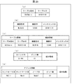
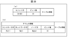
- (A) is a diagram for explaining an example of a network configuration constructed in the communication system according to one aspect of the present disclosure, and (b) is an example of a data structure of address information managed by the network of the communication system. It is a figure which shows. It is a block diagram which shows the structure of the signal processing apparatus, the information transfer apparatus, and the input terminal which concerns on one aspect of this disclosure.
- (A) is a diagram showing an example of a data structure of cable information
- (b) is a diagram showing an example of a data structure of device information
- (c) is a diagram showing an example of a data structure of associated information. It is a figure
- (d) is a figure which shows an example of the data structure of the 1st relay information
- (e) is a figure which shows an example of the data structure of the 2nd relay information.
- It is a flowchart which shows the process flow of each apparatus belonging to the communication system which concerns on one aspect of this disclosure.
- (A) is a diagram showing an example of a data structure of the first intermediate information
- (b) is a diagram showing an example of a data structure of the second intermediate information. It is a flowchart which shows the process flow of each apparatus belonging to the communication system which concerns on one aspect of this disclosure.
- FIG. 2 is a block diagram showing an example of a circuit configuration of an electric device corresponding to a superposed signal and an input unit which is a communication device.
- the electric device 6 limit switch
- the input unit 4 will be described as an example.
- the electrical device 6 and the input unit 4 are connected to each other by a pair of signal lines 21 and 22.
- the signal line 21 is connected to the first input terminal 31 of the input unit 4 and the first terminal 11 of the electric device 6.
- the signal line 22 is connected to the second input terminal 32 of the input unit 4 and the second terminal 12 of the electric device 6.
- a power supply 20 is provided in the path of the signal line 21.
- the power supply 20 is a DC power supply that generates a predetermined voltage (24V in this case).
- the electric device 6 includes a first terminal 11, a second terminal 12, an operating element 13, a potential difference generation circuit 14, and a transmission circuit 15.
- the transmission circuit 15 includes a step-down circuit 16, a data generation circuit 17, a superimposition circuit 18, and a diagnostic circuit 19.
- the operating element 13 is connected between the first terminal 11 and the second terminal 12.
- the potential difference generation circuit 14 is connected in series with the operating element 13 in the energization path between the first terminal 11 and the second terminal 12.
- the potential of the second terminal 12 changes according to the state of the operating element 13. That is, the second terminal 12 outputs an output signal (operating signal) according to the state of the operating element 13 to the outside (signal line 22).
- the transmission circuit 15 is connected between the first terminal 11 and the second terminal 12.
- the transmission circuit 15 operates using the voltage between the first terminal 11 and the second terminal 12 as a power source.
- the step-down circuit 16 steps down the voltage between the first terminal 11 and the second terminal 12 to a predetermined voltage, and outputs a predetermined voltage to the data generation circuit 17.
- the data generation circuit 17 operates by the voltage applied from the step-down circuit 16 to generate transmission data to be transmitted to the input unit 4.
- the transmission data includes, for example, an identifier (ID information) unique to the electric device 6.
- the data generation circuit 17 outputs transmission data to the superimposition circuit 18.
- the superimposition circuit 18 superimposes the received transmission data on the output signal as a data signal. As a result, the transmission circuit 15 outputs the superimposed signal obtained by superimposing the data signal on the output signal from the second terminal 12 to the signal line 22.
- the diagnostic circuit 19 operates by the voltage applied from the step-down circuit 16 and generates diagnostic data representing the diagnostic information of the electric device 6.
- the diagnostic circuit 19 includes a check circuit for an element of the electric device 6 (for example, an operating element 13), and generates diagnostic data indicating whether the electric device 6 is normal or not, depending on whether the output of the check circuit is normal or not. ..
- the diagnostic circuit 19 outputs diagnostic data (diagnostic information) to the data generation circuit 17.
- the data generation circuit 17 may include diagnostic data in the transmission data.
- the input unit 4 includes a first input terminal 31, a second input terminal 32, an input circuit 33, an extraction circuit 34, an error detection circuit 35, and a unit control circuit 36.
- the potential of the first input terminal 31 is maintained constant (for example, GND).
- a superposed signal is input to the second input terminal 32 from the signal line 22.
- the input circuit 33 extracts an output signal from the superimposed signal and outputs the output signal to the unit control circuit 36.
- the extraction circuit 34 extracts a data signal from the superimposed signal and outputs the data signal to the error detection circuit 35.
- the error detection circuit 35 performs error detection on a data signal by using an arbitrary data check method such as CRC check (cyclic redundancy check) or Manchester code check.
- the error detection circuit 35 outputs a data signal and an error detection result to the unit control circuit 36. When an error is detected in the data signal, the error detection circuit 35 does not have to output the data signal to the unit control circuit 36.
- the unit control circuit 36 outputs an output signal and a data signal to the controller 3.
- the error detection circuit 35 and the unit control circuit 36 may be composed of, for example, one integrated circuit or a plurality of integrated circuits.
- FIG. 3 is a block diagram showing a configuration of a communication system including an electric device 6 that supports superimposed signals.
- the communication system 1 includes a PC 2 (personal computer, information processing device), a controller 3, an input unit 4, an output unit 5, and electrical devices 6 to 10.
- the PC 2 is connected to the controller 3.
- the PC 2 receives information related to the electric devices 6 to 10 from the controller 3 and transmits a control command to the controller 3.
- the controller 3 is connected to the input unit 4 and the output unit 5.
- the controller 3 transmits a signal for operating or controlling the electric devices 6 to 10 to the input unit 4 and the output unit 5 according to the control command.
- the controller 3 transmits signals from the electric devices 6 to 10 received via the input unit 4 or the output unit 5 to the PC 2.
- the input unit 4 is a receiving device (communication device), is connected to a plurality of electric devices so as to be able to communicate with each other, and can receive superimposed signals from each electric device.
- electrical devices 6 and 7, respectively, are connected to the input unit 4. That is, the input unit 4 can receive the superimposed signal from the electric devices 6 and 7.
- the input unit 4 periodically receives data signals included in the superimposed signals from the electric devices 6 and 7. It should be noted that the reception of the data signal does not have to be periodic.
- the connection between the input unit and the electrical devices 6 and 7 is made, for example, by a pair of signal lines.
- the input unit 4 can extract a data signal from the received superimposed signal, determine the communication state between the electric device that is the source of the superimposed signal and itself, and output the result to the controller 3. ..
- the input unit 4 can form a communication system 1 as shown in FIG. 3 together with a plurality of devices including the electric devices 6 and 7 and the controller 3.
- the communication error is the value of the operation signal in the electric devices 6 and 7. It can be determined whether or not it can be regarded as occurring during the transition period of.
- Communication errors detected during periods other than the transition period include, for example, communication errors due to repeated momentary interruptions when the switch contacts are in an unstable state, communication errors due to disturbance noise, and wiring disconnection. is there.
- the electric devices 6 and 7 operate by the electric power supplied from the input unit 4, and transmit a signal to the input unit 4 according to the state of the operating elements included in the electric devices 6 and 7.
- the electric device 6 is a limit switch including a switch as an operating element.
- the electric device 7 is a sensor including a sensing element as an operating element.
- the operating element 13 can output an on / off signal as an output signal (operating signal).
- the case where the electric device 6 is a limit switch will be described, but similarly, the case where the electric device 7 is a sensor can also be applied.
- the output unit 5 (communication device) is connected to the electric devices 8 to 10. Each of the electric devices 8 to 10 is connected to the output unit 5 by a pair of signal lines.
- the output unit 5 operates the electric devices 8 to 10 and controls the electric devices 8 to 10 based on the instructions from the PC 2 and the controller 3. Further, the output unit 5 transmits the data signals received from the electric devices 8 to 10 to the controller 3.
- the output unit 5 can receive the superimposed signal from the electric devices 8 to 10 and extract the data signal from the received superimposed signal. Further, the output unit 5 can determine the communication state between the output unit 5 and the electric device. Then, the output unit 5 can output the determination result to the controller 3.
- the electric devices 8 to 10 operate by the electric power supplied from the output unit 5 and are controlled by the control signal received from the output unit 5.
- the electric device 8 is a relay device including a coil as an operating element.
- the electric device 9 is an electromagnetic valve including a coil as an operating element.
- the electric device 10 is an electric actuator including a coil as an operating element.
- FIG. 4 is a diagram schematically showing an example of a signal waveform.
- FIG. 4A shows a case where the cycle of the output signal (operating signal) is longer than the cycle of the data signal
- FIG. 4B shows a case where the cycle of the output signal is shorter than the cycle of the data signal.
- a superposed signal is a superposition of an output signal and a data signal.
- the waveform of the superimposed signal is a waveform obtained by superimposing the waveform of the output signal and the waveform of the data signal.
- the amplitude of the output signal is greater than the amplitude of the data signal. Therefore, the value of the original output signal and the value of the data signal can be known from the superimposed signal.
- the switch of the electric device 6 is ON, the output signal is H, and when the switch of the electric device 6 is OFF, the output signal is L.
- the value of the superimposed signal is divided into L1, L2, H1 and H2 from the lowest. If the superimposed signal is within the L range, the output signal is L. The L range includes L1 and L2. If the superimposed signal is in the H range higher than the L range, the output signal is H. The H range includes H1 and H2. When the superimposed signal is L1 or H1, the data signal is L. When the superimposed signal is L2 or H2, the data signal is H.
- the input unit 4 When the input unit 4 receives the superimposed signal from the electric device 6, it determines whether the output signal is H or L (whether the switch of the electric device 6 is ON or OFF) from the superimposed signal. .. Then, the input unit 4 can extract the data signal from the superimposed signal and output the information corresponding to the data signal to the outside.
- the input unit 4 can determine whether the switch of the electric device 6 is ON or OFF based on the superimposed signal, and further execute the process according to the data signal.
- the input unit 4 can output the identifier and the position information of the electric device 6 to the outside together with the information indicating the disconnection of the wiring.
- the PC 2 classifies the communication state between the input unit 4 and the electric device 6 into three categories, for example, normal, warning, and fault, according to the information received from the input unit 4 via the controller 3. Can be notified.
- the user can determine whether or not maintenance is required for the electric device 6 by acquiring information on the communication state between the input unit 4 and the electric device 6 using the PC 2.
- an input unit 4 that supports the superimposed signal is a device that does not support communication using the superimposed signal (hereinafter,).
- an electric device 6 which is a device that does not support superimposed signal communication When an electric device 6 which is a device that does not support superimposed signal communication) is connected, the electric device does not transmit a data signal to the input unit 4.
- the signal processing device since the input unit 4 cannot extract the data signal from the superimposed signal, only the same processing as the input unit 4 that does not support the superimposed signal can be executed. Therefore, the signal processing device according to one aspect of the present disclosure generates and inputs a superimposed signal superimposed on the operation signal of the electric device 6 by using the predetermined information about the electric device 6 stored in advance as a data signal. Send to unit 4.
- FIG. 1 is a block diagram showing a configuration of a signal processing device 100 and an information rewriting device 200 according to one aspect of the present disclosure.
- the input unit 4 supports communication using superimposed signals.
- the input unit 4 corresponding to the communication using the superimposed signal will be described as a unit electrically connected to the electric devices 6 and 7 via the signal processing device 100.
- the following description can be applied to the output unit 5 as a unit electrically connected to the electric devices 8, 9, and 10 via the signal processing device 100 by the same technical idea. .. That is, it is possible to electrically connect the output unit 5 corresponding to the communication using the superimposed signal and the electric devices 8, 9, and 10 via the signal processing device 100.
- each of the electric devices 6 to 10 may be a device that does not support superimposed signal communication.
- the signal processing device 100 can receive and store predetermined information about the electric device 6 from the information rewriting device 200.
- the signal processing device 100 can generate a superposed signal superimposed on the operation signal of the electric device 6 as a data signal and transmit it to the input unit 4.
- the signal processing device 100 may have a configuration that can be arranged between the electric device 6 and the input unit 4, and may have, for example, a communication cable-like outer shape.
- the signal processing device 100 includes an electric device side terminal 110, a communication device side terminal 120, a light receiving unit 130, an information storage unit 140, and a transmission control circuit 150.
- the transmission control circuit 150 includes a monitoring unit 151, an information rewriting unit 153, and a superposed signal transmission unit 155.
- the electric device side terminal 110 is a terminal for the signal processing device 100 to transmit or receive an output signal with the external electric device 6.
- the electric device side terminal 110 and the electric device 6 are connected by a communication cable or the like.
- the communication device side terminal 120 is a terminal for the signal processing device 100 to transmit or receive an output signal with the input unit 4.
- the communication device side terminal 120 is also a terminal for the signal processing device 100 to transmit a superimposed signal to the information rewriting device 200.
- the input unit 4 and the information rewriting device 200 are connected to one communication device side terminal 120, but they can be selectively connected to either of them.
- the light receiving unit 130 can receive an optical signal from the outside. Specifically, the light receiving unit 130 can receive predetermined information about the electric device 6 from the information rewriting device 200 as an optical signal.
- the light receiving unit 130 may be, for example, a phototransistor (PhotoTR in FIG. 5) that generates a current when receiving light, and the optical signal received by the light receiving unit 130 is transmitted to the information rewriting unit 153.
- the signal processing device 100 may be provided with a window portion that transmits light so that the light receiving unit 130 can efficiently receive an optical signal.
- the information storage unit 140 can store predetermined information about the electric device 6. Predetermined information is written in the information storage unit 140 by the information rewriting unit 153, and the predetermined information is read out by the superimposed signal transmission unit 155.
- the transmission control circuit 150 includes a part of the transmission circuit 15 of FIG. 2 in addition to the monitoring unit 151, the information rewriting unit 153, and the superimposed signal transmission unit 155. That is, the transmission control circuit 150 further includes a data generation circuit 17, a superimposition circuit 18, a diagnostic circuit 19, and the like, which are not shown in FIG.
- the data generation circuit 17, the diagnostic circuit 19, the monitoring unit 151, and the information rewriting unit 153 for example, use the information stored in the memory of the MPU (Micro Processing Unit) to issue program instructions that are software that realizes each unit. It may be realized by executing it.
- MPU Micro Processing Unit
- the monitoring unit 151 can monitor the reception of the optical signal in the light receiving unit 130.
- the monitoring unit 151 may perform monitoring only during a preset monitoring time, or may continue monitoring until the light receiving unit 130 receives an optical signal.
- the monitoring unit 151 can transmit the monitoring result to the superimposed signal transmission unit 155.
- the information rewriting unit 153 can rewrite the information stored in the information storage unit 140 based on an instruction input from the outside. That is, the information rewriting unit 153 can acquire predetermined information from the optical signal received by the light receiving unit 130 and store it in the information storage unit 140. The information rewriting unit 153 may overwrite the predetermined information in the information storage unit 140 according to the type of information, or may store the predetermined information in the information storage unit 140 as history information.
- the superimposition signal transmission unit 155 generates a superimposition signal obtained by superimposing the transmission data (data signal) generated by the data generation circuit 17 on the operation signal output from the operation element 13 of the electric device 6 by the superimposition circuit 18. It can be transmitted to the input unit 4. Specifically, the superimposition signal transmission unit 155 superimposes a data signal generated from predetermined information stored in the information storage unit 140 on the operation signal received from the electric device 6 through the electric device side terminal 110. It is possible to generate a superposed signal. The superimposed signal transmission unit 155 can transmit the generated superimposed signal to the input unit 4 via the communication device side terminal 120.
- the information rewriting device 200 can be communicably connected to the signal processing device 100 and the input terminal 300 described later.
- the information rewriting device 200 can acquire predetermined information about the electric device 6 from the input terminal 300.
- the information rewriting device 200 can project the acquired predetermined information to the signal processing device 100 as an optical signal.
- the information rewriting device 200 receives a superimposed signal from the signal processing device 100 through the communication device side terminal 120, and the predetermined information indicated by the data signal included in the superimposed signal is the same as the content projected by the own device as an optical signal. It is possible to verify whether or not it is done.
- the information rewriting device 200 may output the verification result to a display unit (not shown) or an external device including the input terminal 300.
- the information rewriting device 200 includes a light projecting unit 210 and a rewriting circuit 220, and the rewriting circuit 220 includes an information acquisition unit 221 and an information verification unit 223.
- the light projecting unit 210 can project the predetermined information input from the information acquisition unit 221 as an optical signal.
- the light projecting unit 210 may be, for example, an LED (Light Emitting Diode) (LED in FIG. 5), or may project an optical signal toward the light receiving unit 130 of the signal processing device 100 by an optical cable or the like.
- the optical signal may represent predetermined information, for example, by changing the light projection pattern. Specifically, the light projecting unit 210 may notify predetermined information by using a change in the color of light, a blinking pattern, and the intensity of light.
- the light projecting unit 210 may further project an optical signal indicating the start of rewriting and the end of rewriting before and after projecting an optical signal corresponding to the information to be rewritten.
- the rewriting circuit 220 can execute various functions for rewriting predetermined information about the electric device 6 stored in the information storage unit 140 of the signal processing device 100.
- the rewriting circuit 220 can receive the superimposed signal from the signal processing device 100 through the communication device side terminal 120 and verify the superimposed signal.
- the information acquisition unit 221 can acquire information to be rewritten from the input terminal 300.
- the information acquisition unit 221 inputs the acquired information to the light projection unit 210.
- the information verification unit 223 extracts a data signal from the superimposed signal received from the signal processing device 100, and the predetermined information about the electric device 6 indicated by the data signal is projected as an optical signal from the light projecting unit 210. It is possible to verify whether or not it is done. Specifically, the information verification unit 223 verifies whether or not the information storage unit 140 has been rewritten in the signal processing device 100, and whether or not the predetermined information after the rewriting matches the projected contents. Perform two of the verifications of.
- the input terminal 300 is communicably connected to the information rewriting device 200, and can input predetermined information about the electric device 6 to be stored in the information storage unit 140 of the signal processing device 100 to the information rewriting device 200. It can.
- the input terminal 300 may be, for example, a smartphone, and the user of the input terminal 300 may input predetermined information by a touch operation or the like.
- the information rewriting device 200 may be an adapter that can be connected to a smartphone and has a dedicated light source that operates as a light projecting unit 210.
- the information rewriting device 200 may be connected to a smartphone via USB (Universal Serial Bus).
- the input terminal 300 may be integrally configured with the information rewriting device 200.
- the smartphone may use an LED for display or lighting as the light projecting unit 210.
- the predetermined information regarding the electric device 6 may be input to the input terminal 300 by a method other than manual operation.
- the input terminal 300 reads and acquires the two-dimensional code by using a camera or the like. May be good.
- FIG. 5 is a circuit diagram showing the configuration of the signal processing device 100 and the information rewriting device 200 according to one aspect of the present disclosure. Although some blocks described with reference to FIGS. 1 and 2 are not shown in FIG. 5, they are signal processing devices as shown in FIGS. 1 and 2. It shall be provided in 100 or the information rewriting device 200.
- the electric device side terminal 110 and the communication device side terminal 120 each have two paths.
- the current supplied from the power supply 20 is input to the + terminal side of the communication device side terminal 120, and the current is input to the transmission control circuit 150 through the diode D1. That is, the signal processing device 100 drives the transmission control circuit 150 and the like by the current supplied from the power supply 20.
- the light receiving unit 130 shown as “PhotoTR” in the figure receives an optical signal from the light emitting unit 210 shown as “LED” in the information rewriting device 200 according to the path shown by the broken line, and converts the optical signal. An electric signal is input to the transmission control circuit 150.
- the transmission control circuit 150 transmits / receives currents and signals using the electrical device side terminal 110 and the communication device side terminal 120. Specifically, the transmission control circuit 150 receives an output signal from an electric device 6 (not shown) according to the state of the operating element 13 of the electric device 6 through the terminal 110 on the electric device side, and is stored in the information storage unit 140. Is superposed on the output signal to generate a superposed signal. Further, the transmission control circuit 150 transmits the generated superimposed signal to the rewriting circuit 220 of the information rewriting device 200 through the communication device side terminal 120.
- the transmission control circuit 150 rewrites the predetermined information stored in the information storage unit 140 to the contents input from the light emitting unit 210. be able to. Then, the transmission control circuit 150 can transmit to the rewriting circuit 220 a superposed signal in which various information stored in the information storage unit 140, including the rewritten contents, is superimposed on the output signal. As a result, the information rewriting device 200 can verify whether or not the predetermined information included in the superimposed signal received by the rewriting circuit 220 matches the content projected from the light projecting unit 210.
- FIG. 6 is a diagram showing a specific example of information rewriting and verification using the signal processing device 100 and the information rewriting device 200 on one aspect of the present disclosure. In the following description, it is assumed that the information to be rewritten by using the input terminal 300 has already been input to the information rewriting device 200.
- “DC” indicates the direct current supplied from the power source 20, and “DC-ON” indicates the timing at which the power source 20 is started.
- “(LED-ON)” and “(LED-OFF)” indicate the presence or absence of light projection in the light projecting unit 210.
- "Rewrite start”, “rewrite data”, and “rewrite end” are "a light projection pattern corresponding to a rewrite start instruction indicating the start of rewriting", "a light projection pattern according to the rewrite data to be rewritten”, and Corresponds to each of the "light projection patterns corresponding to the rewriting end instruction indicating the end of rewriting”.
- the "verification mode reception operation” is an operation mode for receiving the superimposed signal transmitted from the signal processing device 100, and the “verification” verifies the predetermined information indicated by the data signal included in the received superimposed signal. The operation mode.
- LED monitoring”, “rewriting mode”, and “normal operation mode transmission operation” indicate operation modes in the signal processing device 100, respectively.
- “LED monitoring” indicates that the monitoring unit 151 monitors the reception of the optical signal in the light receiving unit 130 in the signal processing device 100
- "rewriting mode” indicates that the information rewriting unit 153 in the signal processing device 100 monitors the information storage unit 140. Indicates that the contents of are rewritable.
- the "normal operation mode transmission operation” is a state in which the signal processing device 100 generates a superposed signal in which a data signal indicating predetermined information is superimposed on the output signal acquired from the electric device 6 and transmits the superposed signal to the information rewriting device 200. Shown.
- the information rewriting unit 153 stores the information in the information storage unit 140 based on the optical signal without transmitting the superimposed signal by the superimposed signal transmitting unit 155.
- the operation modes for rewriting are "LED monitoring" and "rewriting mode”. Then, the operation mode in which the superimposed signal transmitting unit 155 transmits the superimposed signal after the rewriting process by the information rewriting unit 153 is completed is the "normal operation mode transmission operation".
- the transmission control circuit 150 of the signal processing device 100 releases the reset state, and after performing the initial processing, the monitoring unit 151 starts monitoring the light reception of the light receiving unit 130 by "LED monitoring".
- the information rewriting device 200 changes the state from "(LED-OFF)" to "(LED-ON)" asynchronously with the state of the signal processing device 100.
- the information rewriting device 200 uses the light projecting unit 210 to project an optical signal in the order of "rewriting start", "rewriting data", and "rewriting end”. After the series of light projection is completed, the information rewriting device 200 shifts the operation mode to the "normal operation mode transmission operation" and starts receiving the superimposed signal.
- the operation mode is changed to the "rewriting mode".
- the information rewriting unit 153 rewrites the information storage unit 140. After that, when the optical signal of the light projection pattern corresponding to the "rewrite end" is received, the "rewrite mode” is ended and the operation mode is changed to the "normal operation mode transmission operation".
- the signal processing device 100 In the "normal operation mode transmission operation", the signal processing device 100 generates a data signal using the rewritten predetermined information stored in the information storage unit 140, and uses the superimposed signal transmission unit 155 to generate the data signal.
- the superposed signal including the superimposed signal is transmitted to the information rewriting device 200.
- the information rewriting device 200 When the information rewriting device 200 receives a superposed signal from the signal processing device 100 during operation in the "normal operation mode transmission operation", after shifting the operation mode to "verification", a predetermined data signal included in the superposed signal indicates. The information in the above is verified using the information verification unit 223.
- the predetermined information about the electric device 6 stored in the signal processing device 100 is rewritten by using the information rewriting device 200. Therefore, the user can rewrite the predetermined information even after the signal processing device 100 is manufactured or shipped. Therefore, the signal processing device 100 can transmit to the input unit 4 a superposed signal in which predetermined information after rewriting is superposed on the output signal received from the electric device 6. Therefore, for example, even when the electric device 6 does not support the superimposed signal transmission, it is possible to realize the superimposed signal transmission by using the signal processing device 100.
- the signal processing device 100 has transitioned the operation mode to the "rewrite mode” based on the optical signal including the rewrite start instruction, but the trigger for the transition to the "rewrite mode” is not limited to this.
- the signal processing device 100 may transition to the "rewrite mode” when the light receiving unit 130 receives some light after the device is started, or may transition based on an input from an external device. ..
- the signal processing device 100 is shown as a device separate from the electric device 6 in the description of FIG. 1, the signal processing device 100 may be integrally configured with the electric device 6.
- the configuration of the signal processing device 100 may be built in the electric device 6.
- FIG. 7 is a flow showing an example of the flow of processing executed by the signal processing device 100 and the information rewriting device 200 according to one aspect of the present disclosure.
- FIG. 7A shows the flow of the signal processing device 100
- FIG. 7B shows the flow of the information rewriting device 200.
- the signal processing device 100 and the information rewriting device 200 are connected to the power supply 20 as in FIG. 5, and information to be rewritten by using the input terminal 300 has already been input to the information rewriting device 200. It shall be.
- the flow of the signal processing device 100 will be described with reference to FIG. 7A.
- the power supply 20 is activated by a user operation or the like
- the supply of electric power to the signal processing device 100 is started (S1).
- the signal processing device 100 releases the reset state when the current supply is started (S2).
- the signal processing device 100 executes the initialization process, and after the initialization process is completed, the monitoring unit 151 starts monitoring the light reception of the light receiving unit 130 (S3).
- the monitoring unit 151 determines whether or not the light receiving unit 130 has detected the optical signal projected from the light emitting unit 210 (S4).
- the light receiving unit 130 receives the light signal.
- the monitoring unit 151 further determines whether or not the light receiving unit 130 has received the rewrite start instruction as an optical signal (S5). ..
- the monitoring unit 151 determines whether or not the preset monitoring time has elapsed (S6).
- the monitoring unit 151 determines whether or not the optical signal indicating the rewriting end instruction, which is projected from the light projecting unit 210 by the process of S16 described later, is received (S9). When it is determined that the reception has not been received (NO in S9), the monitoring unit 151 determines whether or not the preset monitoring time has elapsed (S10). If it is determined that the monitoring time has not elapsed (NO in S10), the process proceeds to S9, and the process of S9 is executed again. On the other hand, when it is determined that the monitoring time has elapsed (YES in S10), the signal processing device 100 ends the acceptance of the rewriting instruction regarding the predetermined information, and the process proceeds to S11.
- the signal processing device 100 starts transmitting the superimposed signal using the superimposed signal transmitting unit 155 (S11).
- the predetermined information indicated by the data signal included in the superimposed signal transmitted in S11 is the content before rewriting when it comes from S6 to S11, and after rewriting by S7 when it comes from S9 or S10 to S11. It becomes the contents of.
- the signal processing device 100 can transmit predetermined information to the communication device as a superposed signal superimposed on the operation signal. Further, it is possible to rewrite the predetermined information included in the content to be transmitted as the superimposed signal based on the optical signal. Therefore, the user can rewrite the predetermined information even after the signal processing device 100 is manufactured or shipped. Further, even if the external electric device 6 is a device that does not support the superimposition signal communication, the superimposition signal transmission can be realized by using the signal processing device 100.
- the flow of the information rewriting device 200 will be described with reference to FIG. 7B.
- the power supply 20 is started by a user operation or the like, the supply of electric power to the information rewriting device 200 is started (S12). If the power supply 20 has already been started by the process of S1 described above, the power supply 20 is not started in S12, and the power supply to the information rewriting device 200 has already started. After that, the information rewriting device 200 starts light projection using the light projecting unit 210 (S13).
- the information rewriting device 200 emits light from the light projecting unit 210 using the rewriting start instruction as an optical signal (S14). After that, the information rewriting device 200 is input from the input terminal 300, and the information acquired by the information acquisition unit 221 is projected as an optical signal from the light projecting unit 210 (S15). When the light projecting unit 210 finishes projecting predetermined information as an optical signal, the information rewriting device 200 uses the light projecting unit 210 to project an optical signal indicating a rewriting end instruction (S16), and then a series of light projections. Is finished (S17).
- the rewriting circuit 220 of the information rewriting device 200 determines whether or not the superimposed signal transmitted by the signal processing device 100 has been received by the process of S11 described above (S18).
- the information verification unit 223 indicates that the predetermined information indicated by the data signal extracted from the superimposed signal is projected by the light projecting unit 210 as an optical signal in S14. It is verified whether or not it matches with (S19).
- the information rewriting device 200 outputs the result verified in S19 to a display unit (not shown) or an external device (S20).
- the information rewriting device 200 can rewrite the information stored in the information storage unit 140 of the signal processing device 100 by an optical signal. Then, the information rewriting device 200 can verify whether or not the information is correctly rewritten from the superimposed signal received from the signal processing device 100.
- the signal processing device 100 is configured to start transmitting the superimposed signal after rewriting the information stored in the information storage unit 140.
- the signal processing device 100 may have a configuration in which information can be rewritten during transmission of, for example, a superposed signal.
- the signal processing device 100 and the information rewriting device 200 will be described with reference to FIG.
- the information rewriting device 200 is the same as the information rewriting device 200 in the configuration example.
- the basic configuration of the signal processing device 100 is the same as that of the configuration example, but some configurations are different.
- the superimposed signal transmitting unit 155 transmits the superimposed signal even while the monitoring unit 151 is monitoring the light received by the light receiving unit 130, and stops transmitting the superimposed signal when the light receiving unit 130 detects the optical signal. The point to do is different.
- FIG. 8 is a diagram showing a specific example of information rewriting and verification using the signal processing device 100 and the information rewriting device 200 during transmission of the superimposed signal.
- information to be rewritten by using the input terminal 300 has already been input to the information rewriting device 200, and the description of the item having the same name as that of FIG. 6 will be omitted. Further, since the operation of the information rewriting device 200 is the same as that in FIG. 6, the description thereof will be omitted.
- the transmission control circuit 150 of the signal processing device 100 releases the reset state, performs initial processing, and then operates in "LED monitoring (normal operation mode)".
- LED monitoring normal operation mode
- the "LED monitoring (normal operation mode)" is an operation mode in which the monitoring unit 151 monitors the light reception of the light receiving unit 130 and the superimposed signal transmitting unit 155 transmits the superimposed signal.
- the signal processing device 100 When the signal processing device 100 detects the reception of an optical signal during operation in the "LED monitoring (normal operation mode)", the signal processing device 100 stops transmitting the superimposed signal and then shifts the operation mode to the "rewrite mode". The signal processing device 100 rewrites information based on the optical signal received from the light projecting unit 210 of the information rewriting device 200 as described above using FIG. 6, and then terminates the "rewriting mode” and "rewrite mode” is completed. Transition the operation mode to "normal operation mode transmission operation". The operation of the signal processing device 100 in the "normal operation mode transmission operation" is the same as that described above with reference to FIG. In this way, the signal processing device 100 can rewrite the information by using the information rewriting device 200 even after the transmission of the superimposed signal is started.
- FIG. 9 is a flow showing an example of a processing flow executed by the signal processing device 100 according to one aspect of the present disclosure. In the following description, the same processing as in FIG. 7A will be omitted. Further, the flow of the information rewriting device 200 is completely the same as that of FIG. 7 (b).
- the signal processing device 100 After executing the processes of S1 and S2, the signal processing device 100 starts transmitting the superimposed signal by the superimposed signal transmitting unit 155 and monitoring the light receiving unit 130 by the monitoring unit 151 (S21). After S21, the signal processing device 100 executes the processes of S4 to S6 in the same manner as in the above operation example.
- the superimposition signal transmission unit 155 since the superimposition signal transmission unit 155 has already started transmitting the superimposition signal in S21, when the monitoring unit 151 determines in S6 that the preset monitoring time has elapsed (YES in S6), a series of series. The point at which the processing is terminated is different from that in FIG. 7A.
- the superimposition signal transmission unit 155 stops the transmission of the superimposition signal (S22). The process then proceeds to S7. On the other hand, when it is determined that the rewrite activation instruction has not been received (NO in S5), the process proceeds to S8, and it is determined whether or not the monitoring time for the rewrite activation instruction has elapsed (S8).
- the monitoring unit 151 determines in S8 that the preset monitoring time has elapsed (YES in S8), a series of series. The point at which the processing is terminated is different from that in FIG. 7A.
- the signal processing device 100 executes the processes of S9 and S10 in the same manner as in the above operation example. Then, when it is determined in S9 that the rewriting end instruction has been received (YES in S9), or when it is determined in S10 that the monitoring time has elapsed (YES in S10), the superimposed signal transmitting unit 155 transmits the superimposed signal. Is restarted (S23). After that, the signal processing device 100 ends a series of processes.
- the signal processing device 100 can rewrite the information based on the optical signal even after the transmission of the superposed signal is started, and can transmit the superposed signal generated by using the rewritten information.
- the information rewriting device 200 is configured to input the information to be rewritten to the signal processing device 100 by the light projection using the light projecting unit 210.
- the information rewriting device 200 may be configured so that, for example, the information to be rewritten can be transmitted to the signal processing device 100 through a path used for transmitting and receiving the superimposed signal.
- FIG. 10 is a block diagram showing a configuration of a signal processing device 100 and an information rewriting device 200 according to one aspect of the present disclosure.
- the basic configuration of the signal processing device 100 is the same as that of the configuration example, but some configurations are different.
- the signal processing device 100 includes a current detection unit 160 instead of the light receiving unit 130 and the monitoring unit 151.
- the current detection unit 160 is connected to the input unit 4 or the information rewriting device 200, and can detect the current value of the current signal supplied from the signal line used for transmitting and receiving the superimposed signal. Specifically, the current detection unit 160 can detect the current value of the current signal input to the communication device side terminal 120 and transmit the detection result to the transmission control circuit 150.
- the transmission control circuit 150 can rewrite the information by the information rewriting unit 153 based on the detection result of the current value by the current detection unit 160. Specifically, when the current detection unit 160 indicates that the fluctuation pattern of the current value of the current signal received by the signal processing device 100 from the input unit 4 or the information rewriting device 200 indicates an information rewriting instruction, the transmission control circuit 150 sets the current signal. Rewrite information based on. In the following description, the current signal indicated by the information rewritten by the fluctuation of the current value is referred to as a rewriting current signal.
- the information rewriting unit 153 is different from the above configuration example in that the information stored in the information storage unit 140 is rewritten based on the rewriting current signal.
- the current value of the rewriting current signal may be in the range of values that can be distinguished from other current signals. For example, if the output signal received from the electric device 6 is an on / off signal, the information rewriting unit 153 detects a current value higher than the current value in the on signal of the output signal by the current detection unit 160. Fluctuations in the current value may be recognized as a rewriting current signal.
- the basic configuration of the information rewriting device 200 is the same as that of the configuration example, but some configurations are different.
- the information rewriting device 200 includes a current control unit 230 instead of the light projecting unit 210.
- the current control unit 230 can generate a rewrite current signal according to predetermined information input from the information acquisition unit 221 and transmit the generated rewrite current signal to the signal processing device 100.
- the current control unit 230 may generate a rewriting current signal using, for example, a current value higher than the current value in the ON signal of the output signal of the electric device 6.
- FIG. 11 is a circuit diagram showing the configuration of the signal processing device 100 and the information rewriting device 200 according to one aspect of the present disclosure. In the following description, the description of the items already explained in FIG. 5 will be omitted.
- the signal processing device 100 includes a current detection unit 160 between the ⁇ side of the communication device side terminal 120 and the transmission control circuit 150.
- the current detection unit 160 is composed of, for example, a resistor or an operational amplifier, and outputs a signal indicating the current value of the current signal detected by the resistor to the transmission control circuit 150 after being amplified and output adjusted by the operational amplifier. be able to.
- the transmission control circuit 150 when the current value of the current signal from the current detection unit 160 is higher than the current value in the on signal of the output signal of the electric device 6, for example, the current signal is a rewriting current signal. Judge that there is.
- the transmission control circuit 150 determines that the current signal is a rewriting current signal
- the information rewriting unit 153 rewrites the information stored in the information storage unit 140 based on the rewriting current signal.
- the current control unit 230 can be realized by combining transistors and resistors as shown in the figure.
- the current control unit 230 is configured as shown in the figure, for example, the current control unit 230 is rewritten by switching ON / OFF of the transistor according to the information received from the input terminal 300 by the information acquisition unit 221 of the rewriting circuit 220. Can generate a current signal.
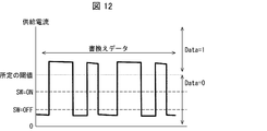
- FIG. 12 is a schematic diagram showing an outline of the rewriting current signal.
- the “supply current” on the vertical axis indicates the current value of the rewriting current signal supplied from the information rewriting device 200 to the signal processing device 100.
- the "predetermined threshold value” is a sufficiently large value as compared with the H range of the superimposed signal.
- the "predetermined threshold value” is shown as a sufficiently large value as compared with the H range of the superimposed signal, but the “predetermined threshold value” is not limited to this.
- the current detection unit 160 can recognize the H range and L range of the superimposed signal, that is, whether the switch of the electric device 6 is ON or OFF, it is “predetermined” according to the state of the switch of the electric device 6.
- the “threshold value of” may be different.
- the signal processing device 100 transmits or receives an output signal which is an off signal due to a reason such as the switch of the electric device 6 being OFF
- the signal processing device 100 corresponds to the L range as a superposed signal. Does not detect the current.
- the current control unit 230 may generate a rewriting current signal with a current value higher than the current value in the off signal of the output signal.
- the information rewriting unit 153 may recognize the fluctuation of the current value as a rewriting current signal.
- a value sufficiently larger than the L range but smaller than the H range is set as " It may be a predetermined threshold value.
- the current value of the rewriting current signal can be made lower than the current value while the switch is ON while the switch of the electric device 6 is OFF.
- FIG. 13 is a diagram showing a specific example of information rewriting and verification using the signal processing device 100 and the information rewriting device 200.
- information to be rewritten by using the input terminal 300 has already been input to the information rewriting device 200, and the description of the item having the same name as that of FIG. 6 will be omitted.
- the transmission control circuit 150 of the signal processing device 100 releases the reset state, performs initial processing, and then operates by "current detection".
- "current detection” is an operation mode in which the current detection unit 160 detects the power value of the current signal.
- the information rewriting device 200 uses the current control unit 230 to control the current value of the current signal supplied to the signal processing device 100 immediately after the power supply 20 is started. After that, the information rewriting device 200 uses the current control unit 230 to control the current value of the current signal supplied to the signal processing device 100 so as to be equal to or higher than a predetermined threshold value, and outputs a current signal corresponding to the rewriting start instruction to the signal processing device. Send to 100. After transmitting the current signal corresponding to the rewriting start instruction, the information rewriting device 200 transmits the information to be rewritten by the "rewriting data" as a rewriting current signal indicating the increase or decrease of the current value. After transmitting the rewriting current signal according to the information to be rewritten, the information rewriting device 200 transmits a current signal corresponding to the rewriting end instruction to the signal processing device 100 at "rewrite end".
- the signal processing device 100 transitions to the "rewrite mode”. Then, the information rewriting unit 153 rewrites the information of the information storage unit 140 based on the rewriting current signal received from the information rewriting device 200 during the operation in the "rewriting mode”. After that, when the rewriting end instruction is received, the information rewriting device 200 ends the "rewriting mode", performs a predetermined process in the "internal process”, and then shifts the operation mode to the "normal operation mode transmission operation".
- the operation of the signal processing device 100 in the "normal operation mode transmission operation” is the same as that described above with reference to FIG. In this way, the signal processing device 100 can rewrite the information based on the rewriting current signal.
- FIG. 14 is a flow showing an example of the flow of processing executed by the signal processing device 100 and the information rewriting device 200 according to one aspect of the present disclosure.
- FIG. 14A shows the flow of the signal processing device 100
- FIG. 14B shows the flow of the information rewriting device 200.
- the same processing as in FIGS. 7A and 7 will be omitted.
- the signal processing device 100 After executing the processes of S1 and S2, the signal processing device 100 starts detecting the current value of the current signal by the current detection unit 160, and determines whether or not a current of a predetermined threshold value or more is detected (S31). .. When the current value of the current signal supplied to the signal processing device 100 increases due to the processing of S41 described later, the current detection unit 160 detects a current equal to or greater than a predetermined threshold value (YES in S31).
- the current detection unit 160 After the current detection unit 160 detects a current equal to or greater than a predetermined threshold value in S31, information to be rewritten from the information rewriting device 200 by the process of S42 described later is transmitted as an increase or decrease in the current value.
- the information rewriting unit 153 of the transmission control circuit 150 rewrites the information of the information storage unit 140 based on the detection result of the current detection unit 160 with respect to the increase / decrease of the current value (S32). After that, the current detection unit 160 determines whether or not a current signal corresponding to the rewrite end instruction has been received from the information rewriting device 200 (S33). If it is determined that the detection has been detected, the transmission control circuit 150 finishes rewriting the information and starts transmitting the superimposed signal using the superimposed signal transmitting unit 155 (S11).
- the signal processing device 100 can receive information to be rewritten via the signal line connected to the input unit 4. Therefore, no special configuration is required to receive the information to be rewritten. Further, since the current signal having a current value higher than the current value in the on signal of the output signal of the electric device 6 is selectively used as the rewriting current signal, the output signal and the rewriting current signal can be clearly distinguished. it can.
- the information rewriting device 200 After executing the process of S12, the information rewriting device 200 increases the current supplied to the signal processing device 100 by using the current control unit 230 (S41). After that, the current control unit 230 generates and transmits a rewriting current signal having the information to be rewritten as an increase / decrease of the current value, which has been acquired by the information acquisition unit 221 (S42). When the transmission of the information to be rewritten is completed, the current control unit 230 generates a current signal indicating the rewrite end instruction in the rewrite end instruction and transmits it to the signal processing device 100 (S43). After S43, the information rewriting device 200 executes the processes of S18 to S20, and verifies the predetermined information indicated by the data signal included in the superimposed signal transmitted from the signal processing device 100 in the process of S11.
- the information rewriting device 200 can rewrite the information stored in the information storage unit 140 by the rewriting current signal transmitted via the signal line included in the signal processing device 100. Further, since the current signal having a current value higher than the current value in the on signal of the output signal of the electric device 6 is selectively used as the rewriting current signal, the output signal and the rewriting current signal are used in the signal processing device 100. It is possible to make a clear distinction.
- the communication between the signal processing device 100 and the information rewriting device 200 is performed by a communication cable connected to the communication device side terminal 120 and capable of transmitting and receiving superimposed signals. Since the input unit 4 can be connected to the signal processing device 100 by a communication cable, for example, the input unit 4 may be built in for various functions provided by the information rewriting device 200 in the modification 2.
- FIG. 15 is a block diagram showing a configuration of a signal processing device 100 and an input unit 4 according to one aspect of the present disclosure. Since the configuration of the signal processing device 100 is the same as the configuration shown in FIG. 10, the description thereof will be omitted.
- the input unit 4 further includes a series of configurations provided by the information rewriting device 200 in the modification 2 in addition to the configurations described in the configuration example. That is, the input unit 4 includes a rewriting circuit 220 and a current control unit 230, and the rewriting circuit 220 includes an information acquisition unit 221 and an information verification unit 223.
- the information acquisition unit 221 is different from the modification 2 in that it acquires predetermined information about the electric device 6 from the PC 2 connected to the input unit 4 via the controller 3.
- the input unit 4 includes an operation signal processing unit 41 and a data signal processing unit 42.
- the operation signal processing unit 41 can detect an output signal (operation signal) from the superimposed signal.
- the operation signal processing unit 41 corresponds to the input circuit 33 in FIG. 2 and transmits the detected output signal to a control circuit (corresponding to the unit control circuit 36 in FIG. 2) (not shown).
- the data signal processing unit 42 can extract a data signal from the superimposed signal.
- the data signal processing unit 42 corresponds to the extraction circuit 34 in FIG. 2, detects an error as necessary, and then transmits the extracted data signal to a control circuit (corresponding to the unit control circuit 36 in FIG. 2). ..
- FIG. 16 is a circuit diagram showing a configuration of a signal processing device 100 and an input unit 4 according to one aspect of the present disclosure.
- the circuit configuration of the signal processing device 100 is the same as that of FIG. 11, and the circuit configuration of the input unit 4 is the same as that of the information rewriting device 200 in FIG.
- the rewriting circuit 220 of the input unit 4 receives predetermined information input from the PC 2 via the controller 3.
- FIGS. 14A and 14B The processing executed by the signal processing device 100 and the input unit 4 according to one aspect of the present disclosure is shown in FIGS. 14A and 14B, except that the input unit 4 is used instead of the information rewriting device 200. Since it is the same as the content, the description thereof will be omitted.
- the communication device that detects the output signal and extracts the superimposed signal can also function as an information rewriting device.
- the superimposed signal has a wide range of current values such as H range and L range. Therefore, when the input unit 4 that does not support the superposed signal is connected to the signal processing device 100, the input unit 4 receives the superposed signal as an output signal, so that the H range and the L range cannot be properly determined, and false detection There is a risk of.
- the signal processing device 100 As a means for preventing erroneous detection, for example, in the signal processing device 100, it is determined whether or not the input unit 4 supports communication using the superimposed signal based on the current value of the current supplied from the input unit 4. Is possible. If it is possible to detect whether or not the input unit 4 supports communication using the superimposed signal, the signal processing device 100 operates by switching, for example, an operation mode for transmitting the superimposed signal and an operation mode for transmitting only the output signal. Can be done.
- the current signal is a rewriting current signal based on the current value, in order to achieve both of these, the current signal is "corresponding to communication using the superimposed signal". It is necessary to execute two processes of "determining whether or not the signal is present” and “converting the rewriting current signal into information to be rewritten”.
- FIG. 17 is a block diagram showing a configuration of a signal processing device 100 and an input unit 4 according to one aspect of the present disclosure.
- the configuration of the input unit 4 is the same as the configuration shown in FIG.
- the signal processing device 100 further includes an operation mode switching unit 157 in addition to the configuration described in the modification 3.
- the signal processing device 100 can operate by switching between a normal operation mode in which the superimposed signal transmission unit 155 transmits the superimposed signal and a low current consumption mode in which the superimposed signal is not transmitted.
- the operation mode switching unit 157 can switch the operation mode of the signal processing device 100 between the normal operation mode and the low current consumption mode based on the detection result in the current detection unit 160.
- the operation mode switching unit 157 changes the operation mode of the signal processing device 100 from the low current consumption mode when, for example, the magnitude or fluctuation pattern of the current value detected by the current detection unit 160 is an instruction to switch to the normal operation mode. You can switch to normal operation mode.
- the basic configuration of the input unit 4 is the same as that of the modification 3, but some configurations are different.
- the current control unit 230 transmits information to be rewritten as a rewriting current signal in the same manner as in the modification 3, and sets the operation mode of the signal processing device 100 between the normal operation mode and the low current consumption mode. It is possible to transmit a current signal corresponding to a switching instruction for switching. By transmitting the current signal corresponding to the switching instruction, the input unit 4 can notify the signal processing device 100 that it corresponds to the superimposed signal. Therefore, it is possible to switch the signal processing device 100 to the normal operation mode and operate it to receive the superimposed signal.
- FIG. 18 is a diagram showing a specific example of information rewriting and operation mode switching using the signal processing device 100 and the input unit 4.
- FIG. 18A shows the rewriting of information
- FIG. 18B shows the switching of the operation mode.
- FIG. 18C shows a specific example of the switching instruction and the rewriting data.
- FIG. 18A is basically the same as FIG. 13 except that the input unit 4 is used instead of the information rewriting device 200.
- the "verification mode reception / compare" is an operation mode for the input unit 4 to receive and verify the superimposed signal transmitted from the signal processing device 100, and the "low current consumption mode” is the low current consumption mode described above. Indicates that there is.
- the operation mode is changed to the "rewrite mode". .. Since the superimposed signal is not transmitted during the operation in the "rewrite mode", the "rewrite mode” is a kind of low current consumption mode.
- the signal processing device 100 rewrites the information storage unit 140 by the information rewriting unit 153 based on the rewriting current signal detected during operation in the "rewriting mode”, and then "rewrite mode” based on the rewriting end instruction. Is terminated, and the operation mode is changed to "normal operation mode transmission operation". That is, when the operation mode switching unit 157 detects the rewriting end instruction, the operation mode can be switched to the normal operation mode.
- the signal processing device 100 In the "normal operation mode transmission operation", the signal processing device 100 generates a data signal using the rewritten predetermined information stored in the information storage unit 140, and uses the superimposed signal transmission unit 155 to generate the data signal.
- the superposed signal including the superimposed signal is transmitted to the information rewriting device 200.
- the input unit 4 transmits the rewriting start instruction, the rewrite data, and the rewrite end instruction as current signals in the same manner as the information rewriting device 200 of FIG. 13, and then receives the superimposed signal in the "verification mode reception / compare". Receive and verify. If there is no problem with the verification result, the input unit 4 operates in the "normal operation mode reception operation" and continues communication using the superimposed signal.
- the instruction for switching from the low current consumption mode to the normal operation mode corresponds to supplying a large current for a certain period of time. .. That is, the input unit 4 supplies a large current for a certain period of time as a switching instruction while the signal processing device 100 is operating in the low current consumption mode.
- the signal processing device 100 determines whether or not the current signal corresponds to the switching instruction by "check", and as a result of determining that it corresponds to the switching instruction, the operation mode switching unit 157 switches the operation mode to the normal operation mode and superimposes the signal. Start transmitting the signal. After supplying a large current corresponding to the switching instruction, the input unit 4 operates in the "normal operation mode reception operation" and starts receiving the superimposed signal.
- FIG. 18C shows an instruction to switch from the low current consumption mode transmitted as a current signal by the input unit 4 to the normal operation mode, and rewriting received as rewrite data by the signal processing device 100 during operation in the “rewrite mode”.
- This is a specific example of a current signal.
- the switching instruction is evaluated, for example, by the duration of the current value. That is, when the current detection unit 160 detects that the pulse width at the beginning of the current signal is equal to or greater than a predetermined pulse width, the signal processing device 100 determines that the current signal is a switching instruction.
- the rewritten data is evaluated by a data string in which fluctuations in the current value are combined as binary values, as explained with reference to FIG.
- the information rewriting unit 153 sends the information storage unit 140 to the information storage unit 140. You may shift to the rewrite mode that rewrites the stored information.
- the information rewriting device 200 supplies a rewriting current signal, which is a predetermined data string, to the signal processing device 100 operating in the low current consumption mode, and then rewrites according to the information to be rewritten.
- a current signal may be supplied.
- FIG. 19 is a flow showing an example of a processing flow executed by the signal processing device 100 according to one aspect of the present disclosure. In the following description, the same processing as in FIG. 7A will be omitted.
- the operation mode switching unit 157 sets the operation mode of the signal processing device 100 to the low current consumption mode (S71).
- the current detection unit 160 starts detecting that a current having a current value equal to or higher than a predetermined threshold value is supplied from the input unit 4 (S72).
- the current detection unit 160 detects that a current having a current value equal to or higher than a predetermined threshold value is supplied from the input unit 4 (YES in S72), and the processing is performed. Proceed to S73.
- the signal processing device 100 determines whether or not the current detection unit 160 has detected the instruction to switch to the normal operation mode by checking whether or not the pulse width of the current signal is equal to or greater than the predetermined pulse width. (S73). If it is determined that the switching instruction has not been detected (NO in S73), the process proceeds to S74. On the other hand, when it is determined that the switching instruction is detected (YES in S73), the operation mode switching unit 157 sets the operation mode of the signal processing device 100 to the normal operation mode (S75), and the superimposed signal transmitting unit 155 sets the superimposed signal. Transmission is started (S78). After that, a series of processes is completed.
- the signal processing device 100 further determines whether or not the current detection unit 160 has received the rewrite start instruction (S74). When it is determined that the rewrite start instruction has not been received (NO in S74), the signal processing device 100 determines whether or not the preset monitoring time has elapsed (S76). If it is determined that the monitoring time has not elapsed (NO in S76), the process proceeds to S74, and the processes of S74 and S76 are executed again. On the other hand, when it is determined that the monitoring time has elapsed (YES in S76), the signal processing device 100 ends the acceptance of the rewriting instruction regarding the predetermined information, and the process proceeds to S11.
- the current detection unit 160 detects this, and the signal processing device 100 says that the current detection unit 160 has received the rewrite start instruction. Judgment (YES in S74). Then, the information rewriting unit 153 rewrites the information of the information storage unit 140 based on the rewriting current signal in which the information to be rewritten is indicated as the increase / decrease of the current value, which is transmitted from the input unit 4 by the process of S42 (S77). After that, the signal processing device 100 executes the processes of S9 to S11, and then ends a series of processes.
- the signal processing device 100 can switch to the normal operation mode when it detects a current of a predetermined threshold value or more with a predetermined pulse width or more while operating in the low current consumption mode.
- the input unit 4 connected to the signal processing device 100 is an input unit corresponding to the reception of the superimposed signal
- the input unit 4 supplies the signal processing device 100 with a current of a predetermined threshold value or more. It can be configured to be.
- the signal processing device 100 can operate in different operation modes depending on whether it is connected to an input unit communication device that supports superimposed signals and if it is connected to an input unit that does not support superimposed signals.
- FIG. 20 is a flow showing an example of a flow of processing executed by the input unit 4 according to one aspect of the present disclosure. In the following description, the same processing as in FIG. 14B will be omitted.
- the input unit 4 transmits a current pulse corresponding to the rewrite start instruction to the signal processing device 100 under the control of the current control unit 230 (S81). After that, the processes S42 to S43 and S18 to S20 are executed, and the series of processes is completed.
- the input unit 4 can rewrite the information stored in the information storage unit 140 by the rewriting current signal transmitted via the signal line included in the signal processing device 100.
- FIG. 21 is a flow showing an example of a flow of processing executed by the input unit 4 according to one aspect of the present disclosure. In the following description, the same processing as in FIG. 14B will be omitted.
- the input unit 4 transmits a current pulse corresponding to an instruction to switch to the normal operation mode to the signal processing device 100 under the control of the current control unit 230 (S91). After that, the input unit 4 controls the current control unit 230 to reduce the current supplied to the signal processing device 100 (S92), and then starts a reception operation for the superimposed signal transmitted from the signal processing device 100 (S93). ..
- the input unit 4 can notify the signal processing device 100 that it is an input unit that supports superimposed signals. Therefore, it is possible to operate the signal processing device 100 in the normal operation mode and receive the superimposed signal. Further, since the signal processing device 100 switches to the normal operation mode when it detects a current equal to or larger than a predetermined threshold value with a predetermined pulse width or more, the signal processing device 100 switches the current supply for switching the mode and the rewriting current signal. It becomes possible to distinguish between.
- FIG. 22 is a diagram schematically illustrating an example of an application situation of the signal processing device 100 according to the present embodiment.
- the communication system 1 includes a PC 2 (personal computer, information processing device), a controller 3, an input unit 4, an output unit 5, and electrical devices 6 to 10.
- the generic term of the input / output unit 52 is used as a conceptual inclusion of these.
- the input / output unit 52 like the input unit 4 and the output unit 5, supports superimposed signal communication. Therefore, the input / output unit 52 includes the respective parts shown in FIG. 2 that the input unit 4 and the output unit 5 are provided to support the superimposed signal communication.
- the electric devices 53 when it is not necessary to individually identify the electric devices 6 to 10, these are simply referred to as the electric devices 53.
- the electrical device 53 is assumed to be a device that does not support superimposed signal communication.
- the signal processing device 100 for processing the superimposed signal is provided between the communication cable 51 connecting the input / output unit 52 and the electric device 53. Therefore, the signal processing device 100 has a cable housing 50 (housing) having a communication cable-like outer shape that can be electrically connected to the communication cable 51.
- one end of the cable housing 50 can be attached to and detached from the communication cable 51 connected to the electric device 53 which is a device that does not support superimposed signal communication.
- the signal processing device 100 and the electric device 53 are electrically connected, and between the signal processing device 100 and the electric device 53.
- the operation signal can be transmitted and received.
- the cable housing 50 incorporating the signal processing device 100 and the electric device 53 are connected in a one-to-one relationship. In the present embodiment, since the electric device 53 is a device that does not support superimposed signal communication, the superimposed signal is not transmitted / received.
- the other end of the cable housing 50 can be connected to the input / output unit 52.
- the other end of the cable housing 50 is configured to be detachably attached to and from the communication cable 51 connected to the input / output unit 52. While the communication cable 51 on the input / output unit 52 side and the other end of the cable housing 50 are connected, the input / output unit 52 and the signal processing device 100 are electrically connected, and the input / output unit 52 and the signal processing device are connected.
- Superimposition signals can be transmitted and received to and from 100.
- the superimposed signal transmitted from the input / output unit 52 to the signal processing device 100 includes, for example, an operation signal for controlling an operation element of the electric device 53 connected to the signal processing device 100.
- the superimposed signal transmitted from the signal processing device 100 to the input / output unit 52 includes, for example, an operating signal according to the state of the operating element of the electric device 53 connected to the signal processing device 100, and the electric device 53 or the electric device 53 or the said.
- a data signal indicating predetermined information about the signal processing device 100 is included.
- information unique to the electric device 53, such as the serial number of the electric device 53, is included as a data signal.
- the electric device 53 is connected to the signal processing device 100 corresponding to the superimposed signal communication on a one-to-one basis, and is connected to the input / output unit 52 via the signal processing device 100. Therefore, even if the electric device 53 is a device that does not support superimposed signal communication, the input / output unit 52 superimposes a data signal unique to the electric device 53 on the operation signal and exchanges the data signal with the signal processing device 100. be able to. Therefore, a device that does not support superimposed signal communication can be used by incorporating it into a communication system that uses the superimposed signal, similarly to an electric device that supports superimposed signal communication. As a result, the degree of freedom in system construction is increased and convenience is improved.
- One input / output unit 52 has a plurality of communication ports, is connected to the signal processing devices 100 in the plurality of cable housings 50 through each communication port, and transmits / receives superposed signals to and from each of the signal processing devices 100. To do. As a result, the input / output unit 52 can monitor and control a plurality of electric devices 53. That is, the input / output unit 52 can form a master module for superimposed signal communication in which each signal processing device 100 is a slave.
- the signal processing device 100 (or the cable housing 50) and the electric device 53 are used. It is necessary that the correspondence with the above is grasped in various devices upstream from the input / output unit 52.
- the various upstream devices specifically refer to a controller 3, a PC2, a server that is communicably connected to a PC2 (not shown), and the like.
- the input terminal 300 (terminal device) is introduced into the communication system 1.
- the input terminal 300 generates associative information indicating the correspondence between the signal processing device 100 (or the cable housing 50) and the electric device 53, and provides the information to various upstream devices.
- the cable housing 50 is configured to be connectable to the input terminal 300 at the other end described above.
- the other end of the cable housing 50 is configured to be detachably attached to and from the information transfer device 200A (200B) externally or built in the input terminal 300.
- the other end of the cable housing 50 is not connected to the input / output unit 52, the other end can be connected to the input terminal 300, to be exact, the information transfer device 200A (200B).
- the input terminal 300 and the signal processing device 100 are electrically connected, and the input terminal 300 is connected. Can send and receive data to and from the signal processing device 100.
- the input terminal 300 can read at least predetermined information from the signal processing device 100.
- the predetermined information read from the signal processing device 100 by the input terminal 300 is, for example, information unique to the signal processing device 100 (or cable housing 50) (hereinafter, cable information).
- the input terminal 300 may be able to write predetermined information to the signal processing device 100, if necessary.
- the information transfer device 200A (200B) like the information rewriting device 200, connects the signal processing device 100 and the input terminal 300 so as to be communicable.
- the information transfer device 200A (200B) includes at least a mechanism for reading out predetermined information stored in the information storage unit 140 of the signal processing device 100.
- the information transfer device 200A (200B) includes a mechanism for writing predetermined information to the information storage unit 140 of the signal processing device 100, that is, each unit included in the information rewriting device 200 shown in FIG. May be good.
- associating information indicating the correspondence between the signal processing device 100 (or the cable housing 50) and the electric device 53 is generated in the input terminal 300 and provided to various upstream devices. Therefore, for example, the PC 2 can monitor and control all the electric devices 53 belonging to the communication system 1 regardless of whether or not they support superimposed signal communication.
- the following description is merely an example of the configuration of the communication system 1 including the input / output unit 52 according to the present disclosure, and is not intended to be limited to the input / output unit 52 connected to the network. ..
- the input / output unit 52 may be connected to the controller 3 without going through the network. That is, such an input / output unit 52 which is an input / output unit 52 connected to the system bus of the controller 3 and has a superimposed communication function also falls within the category of the present invention.
- FIG. 23A is a diagram illustrating an example of a network configuration constructed in the communication system 1 to which the signal processing device 100 is applied.
- FIG. 23B is a diagram showing an example of a data structure of address information managed by the network of communication system 1.
- the PC 2 is communicably connected to one or more controllers 3.
- the PC 2 identifies the controller 3 which is a communication partner based on the identification information (hereinafter, controller ID) unique to the controller 3.
- Controller 3 may be connected to one or more networks. Then, it is communicably connected to one or more input / output units 52 via one network.
- the controller 3 identifies each network based on the identification information (hereinafter, network ID) unique to each network. Further, when the controller 3 communicates with a plurality of input / output units 52 via one network, the identification information assigned to each input / output unit 52 managed as a node on the network (hereinafter referred to as , Node ID), the input / output unit 52 that is the communication partner is identified. Specifically, the controller 3 grasps the correspondence between the unit ID that identifies the input / output unit 52 and the node ID.
- the controller 3 identifies the node ID based on the unit ID of the input / output unit 52 which is the communication partner, and uses the node ID as a part of the address information on the network of the input / output unit 52 as an upstream device (for example,). , Can be passed to PC2).
- the input / output unit 52 is communicably connected to a plurality of electric devices 53 via a plurality of communication ports included in the own device and a plurality of cable housings 50.
- the input / output unit 52 is connected to the signal processing devices 100 (and a plurality of electric devices 53) in the plurality of cable housings 50, the input / output unit 52 is based on the bit values individually assigned to the communication ports.
- the signal processing device 100 which is the communication partner is identified.
- the input / output unit 52 grasps the correspondence between the cable information (first identification information), which is information unique to the cable housing 50 (signal processing device 100), and the bit value.
- the input / output unit 52 identifies a bit value based on the cable information of the cable housing 50 (signal processing device 100) which is a communication partner, and uses the bit value as a part of the address information on the network of the electric device 53. , Can be passed to an upstream device (eg, controller 3).
- an upstream device eg, controller 3
- the PC 2 communicates under the jurisdiction of the PC 2 based on the address information composed of the controller ID of the controller 3, the network ID, the node ID and the bit value passed from the downstream. It is possible to individually identify all the electrical devices 53 belonging to the system 1 and identify their location on the network.
- the information transfer device 200A connected to the input terminal 300 is a mechanism for writing information to the signal processing device 100 in addition to a mechanism for reading information from the signal processing device 100 in the cable housing 50. have.
- the association information generated by the input terminal 300 is output to the signal processing device 100, and is supplied from the signal processing device 100 to the input / output unit 52 and the PC 2 via the communication cable 51.
- FIG. 24 is a block diagram showing the configurations of the signal processing device 100, the information transfer device 200A, and the input terminal 300 according to one aspect of the present disclosure. It is assumed that the input / output unit 52 shown in the figure supports communication using superimposed signals, similarly to the input unit 4 and the output unit 5.
- the signal processing device 100 has the same configuration as the signal processing device 100 described in the first embodiment except that it is built in the cable housing 50.
- the information storage unit 140 can store predetermined information about the electric device 53, and also stores cable information which is information unique to the cable housing 50 (signal processing device 100). ing.
- the cable information is determined in advance at the time of manufacture or shipment of the cable housing 50 incorporating the signal processing device 100, and is stored in the information storage unit 140, for example.
- the area for storing predetermined information about the electric device 53 and the area for storing the cable information are configured by different IC memories. May be done.
- the former may be composed of a user programmable ROM such as EEPROM (registered trademark) (Electrically Erasable Programmable Read Only Memory) that can be written from the input terminal 300, and the latter may be different from the former.
- EEPROM may be an EEPROM in which writing is prohibited after being set at the time of shipment.
- the information transfer device 200A includes a mechanism for reading information stored in the signal processing device 100 in addition to a mechanism for writing information to the signal processing device 100 included in the information rewriting device 200 described in the first embodiment. I have.
- the information transfer device 200A includes a transfer circuit 220A instead of the rewrite circuit 220 of the information rewrite device 200.
- the transfer circuit 220A is typically composed of hardware such as an MPU (Micro Processing Unit) and an FPGA (Field-Programmable gate array).
- the transfer circuit 220A differs from the rewrite circuit 220 of the first embodiment in that it further has a second information acquisition unit 225.
- the information acquisition unit 221 of the first embodiment will be referred to as a first information acquisition unit 221 in order to easily distinguish it from the second information acquisition unit 225.
- the first information acquisition unit 221 refers to the same information acquisition unit 221 of the first embodiment.
- the first information acquisition unit 221 and the information verification unit 223 and the second information acquisition unit 225 of the transfer circuit 220A are, for example, software that realizes each unit by using information stored in a memory (not shown) by the MPU. It may be realized by executing an instruction.
- the second information acquisition unit 225 acquires cable information from the signal processing device 100 and transfers it to the input terminal 300 in accordance with an instruction from the input terminal 300. Specifically, the second information acquisition unit 225 receives the superimposed signal transmitted from the superimposed signal transmitting unit 155 of the signal processing device 100 via the second input terminal 32, controls the extraction circuit 34, and superimposes the signal. A data signal indicating cable information is extracted from the signal. The second information acquisition unit 225 controls the error detection circuit 35 to perform error detection on the extracted data signal. The second information acquisition unit 225 controls, for example, an FPGA or the like to transfer a data signal indicating cable information and an error detection result to a memory (not shown) that can be read by the input terminal 300.
- the input terminal 300 can read the cable information held by the signal processing device 100 in the cable housing 50 from the memory and process it.
- the input terminal 300 serves as a tool for managing the link information between the signal processing device 100 and the electric device 53 in the cable housing 50, and includes an execution unit (for example, an application) that manages the link information and a user. It provides the user interface required for operation.
- the input terminal 300 is typically composed of a smartphone, a tablet, a notebook computer, a dedicated terminal, or the like.
- the input terminal 300 includes a control unit 310, an input unit 311 and a display unit 312, and a peripheral device interface (not shown).
- the input terminal 300 may include a communication unit 313, if necessary.
- the control unit 310 controls each unit of the input terminal 300 in an integrated manner.
- the control unit 310 may be, for example, a processor that executes a program instruction.
- a processor for example, a CPU (Central Processing Unit), an MPU, or the like can be used.
- the control unit 310 according to the example shown in FIG. 24 has each block of the device information acquisition unit 301, the cable information acquisition unit 302, the information linking unit 303, and the linking information output unit 304.
- Each of the above-mentioned parts shown as a block may be realized by, for example, the CPU or MPU reading a program stored in a storage device such as a ROM (read only memory) into a RAM (random access memory) or the like and executing the program. Good.
- control unit 310 provides basic tools (telephone application, e-mail application, address book management application, camera application, 2) provided by a general mobile terminal when the input terminal 300 is a mobile terminal such as a smartphone. It may include a block (not shown) for realizing (such as a dimensional code reader application).
- the input unit 311 supports the user to input information to the input terminal 300.
- the input unit 311 for example, a touch panel, a camera (imaging unit), a microphone, or the like is assumed.
- the input unit 311 is configured as a touch panel, the touch panel is integrally formed with the display unit 312 described later.
- the input unit 311 as a touch panel receives the input operation of the user and outputs the information corresponding to the input operation to the control unit 310 of the input terminal 300.
- the display unit 312 presents the information processed by the control unit 310 so that the user can visually recognize it.
- the display unit 312 is composed of a liquid crystal display (LCD; Liquid Crystal Display), an organic EL (Electro-Luminescence) display, or the like.
- the communication unit 313 communicates with an external device such as a PC2.
- the communication unit 313 may communicate with the PC 2 by a wireless LAN (Local Area Network), a wired LAN, or an Internet communication realized via a mobile phone network. Further, the communication unit 313 may communicate with the PC 2 by Bluetooth (registered trademark), short-range wireless communication realized via infrared rays, or the like.
- the peripheral device interface connects the input terminal 300 and the external device so as to be communicable.
- the peripheral device interface may include, for example, an adapter for connecting to an external information transfer device 200A via USB (Universal Serial Bus), or an external device such as a USB memory or SD card.
- An adapter for writing data to the information storage medium and reading data from the information storage medium may be included.
- the input terminal 300 may be integrally configured with the information transfer device 200A.
- the device information acquisition unit 301 of the control unit 310 acquires device information (second identification information) unique to the electrical device 53.
- the method by which the device information acquisition unit 301 acquires the device information is not particularly limited.
- the input unit 311 acquires an image (two-dimensional code image) of the two-dimensional code (printing medium) attached to the electric device 53. It is supplied to the device information acquisition unit 301.
- the device information acquisition unit 301 extracts the device information included in the two-dimensional code by the image recognition process.
- the input unit 311 may acquire an image of a sticker (printing medium) on which information such as a model and a serial number attached to the electric device 53 is printed and supply the image to the device information acquisition unit 301.
- the device information acquisition unit 301 may read a character string appearing in an image by OCR (Optical Character Recognition) and generate device information based on the text data of the read character string.
- OCR Optical Character Recognition
- the device information acquisition unit 301 displays an input support graphical user interface (Graphical User Interface) (hereinafter referred to as GUI) for the user to input device information. To display.
- GUI graphical User Interface
- the device information acquisition unit 301 may generate device information based on the information input according to the touch operation on the input unit 311 via the input support GUI.
- the device information acquisition unit 301 converts the user's voice acquired by the input unit 311 into text data by voice recognition processing, and generates device information based on the text data. You may.
- the cable information acquisition unit 302 acquires cable information unique to the signal processing device 100 in the cable housing 50.
- the cable information acquisition unit 302 is the second information transfer device 200A so that the cable information is transferred from the information storage unit 140 of the signal processing device 100 to the memory readable by the input terminal 300. It controls the information acquisition unit 225.
- the information linking unit 303 links the device information acquired by the device information acquisition unit 301 with the cable information acquired by the cable information acquisition unit 302, and indicates the linking relationship between the device information and the cable information. Generate information.
- the linking information output unit 304 outputs the linking information so that the linking information generated by the information linking unit 303 is supplied to the PC2.
- the linking information output unit 304 instructs the information transfer device 200A to write the generated linking information to the signal processing device 100.
- FIG. 25A is a diagram showing an example of a data structure of cable information.
- the cable information is information including identification information unique to the signal processing device 100 in the cable housing 50.
- the cable information is composed of a cable type item and a cable ID item.
- the cable model item information indicating the model of the signal processing device 100 as a product is stored.
- the item of cable ID a serial number for uniquely identifying the signal processing device 100 of the type is stored.
- the signal processing device 100 is uniquely identified by the cable type and the cable ID.
- the illustrated cable information is stored in the information storage unit 140 of the signal processing device 100 in advance at the time of manufacturing, and is read out by the information transfer device 200A as needed.
- each upstream device can recognize that the cable housing 50 has been replaced based on the new cable information.
- FIG. 25B is a diagram showing an example of a data structure of device information.
- the device information is information including identification information unique to the electric device 53.
- the device information is composed of each item of device model, device ID, and maintenance date.
- the device model item information indicating the model of the electric device 53 as a product is stored.
- the item of the device ID a serial number for uniquely identifying the electric device 53 of the type is stored.
- the electric device 53 is uniquely identified by the device model and the device ID.
- the device information acquisition unit 301 may read the device model and the device ID from the two-dimensional code attached to the electric device 53 or the image on which the sticker is copied.
- the latest maintenance implementation date for the electrical device 53 is stored.
- the maintenance date of the electric device 53 may be input by the user, for example, via the input unit 311 as a touch panel.
- the device information acquisition unit 301 may generate device information by associating the device model and device ID read by the image recognition process with the maintenance date input by the user.
- FIG. 25 (c) is a diagram showing an example of the data structure of the association information.
- the linking information is information indicating the connection relationship between the cable housing 50 (signal processing device 100) and the electric device 53, and is generated by the information linking unit 303 in response to a user input operation.
- the associative information is composed of an item for storing cable information and an item for storing device information.
- the information linking unit 303 displays, for example, a GUI for supporting the linking of the cable housing 50 and the electric device 53 on the display unit 312, and receives from the user the cable information to be linked and the designation of the device information.
- the information linking unit 303 links the cable information specified by the user with the device information via the GUI to generate the illustrated linking information.
- the linking information generated by the information linking unit 303 is written to the information storage unit 140 of the signal processing device 100 via the information transfer device 200A.
- the linking information shown in FIG. 25 (c) is placed on the superimposed signal and the signal is transmitted via the communication cable 51. It is transmitted from the processing device 100 to the input / output unit 52.
- FIG. 25D is a diagram showing an example of the data structure of the first relay information.
- the first relay information is information generated when the input / output unit 52 that has received the association information from the signal processing device 100 transfers the association information to the controller 3.
- the first relay information has, for example, a configuration in which a unit ID and a bit value are added to the association information shown in (c) of the figure.
- the bit value assigned to the communication port that has received the association information and the unit ID of its own device are used as the association information.
- the first relay information is generated.
- the input / output unit 52 transfers the generated first relay information to the controller 3.
- FIG. 25 (e) is a diagram showing an example of the data structure of the second relay information.
- the second relay information is information generated when the controller 3 that has received the first relay information from the input / output unit 52 transfers the first relay information to the PC 2.
- the second relay information has, for example, a configuration in which the address information shown in FIG. 23 (b) is added to the association information shown in FIG. 25 (c).
- the controller 3 receives the first relay information from the input / output unit 52
- the controller 3 receives the network ID of the network to which the source input / output unit 52 belongs and the input / output based on the unit ID included in the first relay information.
- the node ID assigned to the unit 52 is specified.
- the controller 3 adds the controller ID of the own device, the specified network ID, the node ID, and the address information including the bit value included in the first relay information to the association information to generate the second relay information. To do.
- the controller 3 transfers the generated second relay information to the PC 2.
- FIG. 26 is a diagram showing an example of the data structure of the configuration table.
- the configuration table is a database of a plurality of second relay information transmitted from each controller 3, and is generated and managed by the PC 2 as an example.
- the configuration table is composed of, for example, an item for storing address information and an item for storing association information.
- the linking information is configured by linking an item for storing cable information and an item for storing device information.
- the PC 2 When the PC 2 receives the second relay information from the controller 3, the PC 2 registers the record corresponding to the received second relay information in the configuration table. For example, when the PC 2 receives the second relay information shown in FIG. 25 (e) from the controller 3, the PC 2 registers the second relay information in the configuration table as a shaded record in FIG. 26. By generating the configuration table, the PC 2 can grasp what kind of electric device 53 is connected to which place on the network.
- the PC 2 obtains associative information including device information of the electric device 53, which is a device that does not support superimposed signal communication, from the signal processing device 100 in all the cable housings 50 in the communication system 1, the input / output unit 52 and the controller 3. Can be obtained via.
- the communication system 1 that supports superimposed communication it is possible to manage information unique to the devices that do not support superimposed signal communication belonging to the communication system 1. For example, when the maintenance date is included in the device information, it is possible to manage the latest maintenance date of each electric device 53 belonging to the communication system 1.
- FIG. 27 is a flowchart showing a processing flow of each device belonging to the communication system 1.
- the work steps (HS1 to HS4) performed by the user are also shown for reference.
- the flowchart shown in FIG. 27 shows, as an example, a flow of a series of processes when a new electric device 53 is installed in the communication system 1.
- the processing procedure described below is only an example, and each processing may be changed as much as possible. Further, with respect to the processing procedure described below, steps can be omitted, replaced, and added as appropriate according to the embodiment.
- the user first installs a new electric device 53 at a predetermined location in the communication system 1. Then, the user connects one end of the cable housing 50 containing the signal processing device 100 to the electric device 53.
- the user connects the other end of the cable housing 50 to the input terminal 300.
- the input terminal 300 and the cable housing 50 are connected via the information transfer device 200A.
- the input terminal 300 provided with the mechanism of the information transfer device 200A may be directly connected to the cable housing 50.
- the control unit 310 of the input terminal 300 associates the cable information with the device information according to the input operation of the user or when the input terminal 300 is connected to the cable housing 50. (For example, an information management application) is started.
- Each unit of the device information acquisition unit 301, the cable information acquisition unit 302, the information linking unit 303, and the linking information output unit 304 included in the control unit 310 may be a part of the information management application.
- the cable information acquisition unit 302 controls the information transfer device 200A to acquire cable information from the signal processing device 100. Specifically, the cable information acquisition unit 302 instructs the information transfer device 200A to read the cable information.
- the second information acquisition unit 225 of the information transfer device 200A performs superimposed communication with the signal processing device 100 and requests cable information from the signal processing device 100.
- the superposed signal transmitting unit 155 of the signal processing device 100 puts the cable information stored in the information storage unit 140 on the superposed signal and sends it to the information transfer device 200A in accordance with the request.
- the second information acquisition unit 225 transfers the cable information extracted from the received superimposed signal to a memory accessible to the input terminal 300.
- the device information acquisition unit 301 reads the transferred cable information from the memory and acquires it.
- the device information acquisition unit 301 acquires the device information of the electrical device 53.
- the device information acquisition unit 301 may extract the device information from the image obtained by photographing the sticker on which the two-dimensional code or the manufacturing information attached to the electric device 53 is printed with a camera, or the user. May acquire the device information input via the GUI.
- the information linking unit 303 In S106 (generation step), the information linking unit 303 generates linking information by associating the cable information acquired in S102 with the device information acquired in S105. For example, the information linking unit 303 links the designated cable information and device information in response to receiving the designation of the cable information and the device information via the GUI.
- the linking information output unit 304 outputs the generated linking information so that the PC2 can receive it. Specifically, the association information output unit 304 instructs the information transfer device 200A to write the association information.
- the first information acquisition unit 221 reads the associated information instructed to be transferred from the memory accessible to the input terminal 300, and for example, as described in the first embodiment, the first information acquisition unit 221 reads the association information instructed to be transferred via the light projecting unit 210.
- the association information is transferred to the signal processing device 100.
- the information rewriting unit 153 writes the association information indicated by the optical signal received from the information transfer device 200A to the information storage unit 140.
- the information rewriting unit 153 determines that the writing is complete. When the writing is completed, the process proceeds from YES in S110 to S111.
- the superimposition signal transmission unit 155 returns the superimposition signal for verification of the written data to the information transfer device 200A.
- the information verification unit 223 verifies the success or failure of the writing as described in the first embodiment.
- the information verification unit 223 returns the verification result to the input terminal 300.
- the association information output unit 304 determines the success or failure of writing based on the verification result. If the writing has failed, the linking information output unit 304 may return from NO in S114 to S107 and instruct the information transfer device 200A to write the linking information again. If the writing is successful, the process proceeds from YES in S114 to S115.
- the linking information output unit 304 may notify the user that the linking information generated according to the user's instruction has been successfully written to the signal processing device 100 in the cable housing 50. For example, the message of writing success is displayed on the display unit 312 of the input terminal 300.
- the user confirms that the associated information has been successfully written in the signal processing device 100, and removes the information transfer device 200A from the cable housing 50.
- the user connects the other end of the removed cable housing 50 to the communication cable 51 connected to the input / output unit 52.
- the connection between the signal processing device 100 and the input terminal 300 is released, and the signal processing device 100 is electrically communicably connected to the input / output unit 52 via the other end of the cable housing 50. ..
- the user turns on the power of the controller 3 and the input / output unit 52.
- the input / output unit 52 acquires the association information (for example, (c) of FIG. 25) from the signal processing device 100. Specifically, the input / output unit 52 requests the association information from the signal processing device 100 in the newly connected cable housing 50.
- the superimposed signal transmission unit 155 puts the requested linking information on the superimposed signal and transmits it to the input / output unit 52 via the communication cable 51.
- the input / output unit 52 adds the bit value assigned to the communication port that received the association information and the unit ID of the own device to the acquired above-mentioned association information, and adds the first relay information (for example, the association information). (D) of FIG. 25 is generated.
- the input / output unit 52 transmits the generated first relay information to the controller 3.
- the controller 3 identifies the address on the network of the input / output unit 52, that is, the network ID and the node ID, based on the unit ID of the input / output unit 52 that is the source of the first relay information.
- the controller 3 associates the address information including the controller ID of the own device, the specified network ID and the node ID, and the bit value included in the first relay information with the above-mentioned association included in the first relay information.
- the second relay information (for example, (e) of FIG. 25) is generated.
- the controller 3 transmits the generated second relay information to the PC2.
- the PC 2 registers the second relay information received from each controller 3 as a record in the configuration table (for example, FIG. 26).
- the electric device 53 which is a device that does not support superimposed signal communication
- the PC 2 manages the information unique to the electric device 53, and the cable housing 50. It is possible to control the electric device 53 by superimposition communication.
- the communication system 1 can also cope with a situation in which an electric device 53 fails and the electric device 53 is replaced with a new one.
- the signal processing device 100 connected to the electric device 53 puts, for example, failure status information on the superimposed signal as predetermined information about the electric device 53, and the input / output unit 52. Send to.
- the failure status information is transmitted to the PC 2 via the input / output unit 52 and the controller 3.
- the address information is added in the same manner as when the association information is transferred, so that the PC 2 can locate the electrical device 53 in which the failure has occurred.
- the user can identify the electric device 53 in which the failure has occurred and start the replacement work of the electric device 53 based on the notification of the failure output by the PC2.
- the user first turns off the power of the controller 3 and the input / output unit 52, and disconnects the communication cable 51 on the input / output unit 52 side from the other end of the cable housing 50. Then, the user connects the other end of the cable housing 50 to the information transfer device 200A of the input terminal 300.
- the cable information acquisition unit 302 acquires the cable information from the signal processing device 100 in the same manner as in S102 to S104.
- the cable information acquisition unit 302 may display the acquired cable information on the display unit 312.
- the user collates the notification output by the PC 2 with the displayed cable information, and the electric device 53 connected to the removed cable housing 50 is undoubtedly a failed electric device to be replaced. It can be confirmed that it is 53.
- the user removes the communication cable 51 on the electric device 53 side from one end of the cable housing 50 to remove the failed electric device 53. Instead, the user connects and installs the new electrical device 53 and the cable housing 50 via the communication cable 51.
- the device information acquisition unit 301 acquires the device information of the newly installed electric device 53 as in S105.
- the device information acquisition unit 301 may acquire the device model and the device ID from the device information from the two-dimensional code.
- the device information acquisition unit 301 may acquire the date on which the exchange was performed from a storage unit (not shown) of the input terminal 300, or may acquire the date input by the user.
- the information linking unit 303 associates the previously acquired cable information with the device information of the new electric device 53 to link the information, as in S106. Is regenerated.
- the generated linking information is supplied to the PC2 and managed by the PC2 in the same manner as in S107 to S121.
- the communication system 1 can cope with a situation where the communication cable 51 connecting the input / output unit 52 and the cable housing 50 is disconnected and the communication cable 51 is replaced with a new one.
- the input / output unit 52 cannot communicate with the signal processing device 100 connected via the broken communication cable 51.
- the input / output unit 52 transmits the bit value specified based on the communication port where the communication is interrupted, the status information of the disconnection, and the unit ID of the own device to the controller 3.
- the disconnection status information is transmitted to the PC 2 via the controller 3.
- the address information is added in the same manner as when the association information is transferred, so that the PC2 has a communication cable 51 between the input / output unit 52 and which cable housing 50. Can be determined if the wire is broken.
- the user identifies which cable housing 50 between the input / output unit 52 and the cable housing 50 has a disconnection based on the notification regarding the disconnection output from the PC 2, and the input / output unit 52 and the cable housing 50 are connected to each other.
- the replacement work of the communication cable 51 between them can be started.
- the user first turns off the power of the controller 3 and the input / output unit 52, and disconnects the communication cable 51 on the input / output unit 52 side from the other end of the cable housing 50. Then, the user connects the other end of the cable housing 50 to the information transfer device 200A of the input terminal 300.
- the cable information acquisition unit 302 acquires the cable information from the signal processing device 100 in the same manner as in S102 to S104.
- the cable information acquisition unit 302 may display the acquired cable information on the display unit 312.
- the user can compare the notification output by the PC 2 with the displayed cable information, and the communication cable 51 connected to the removed cable housing 50 on the input / output unit 52 side is definitely the target of replacement. It can be confirmed that the communication cable 51 is broken.
- the user removes the broken communication cable 51 from the input / output unit 52 and replaces it with a new communication cable 51.
- the device information acquisition unit 301 updates the maintenance date in the device information.
- the device information acquisition unit 301 may acquire the date when the exchange was performed from a storage unit (not shown) of the input terminal 300, or may acquire the date input by the user.
- the maintenance date of the electric device 53 and the replacement date of the communication cable 51 may be treated as different items in the device information. In this case, the device information acquisition unit 301 may update the replacement date of the communication cable 51 with respect to the device information of the electric device 53.
- the information linking unit 303 associates the previously acquired cable information with the updated device information in the same manner as in S106, thereby linking the device information. Is regenerated.
- the generated linking information is supplied to the PC2 and managed by the PC2 in the same manner as in S107 to S121.
- the information transfer device 200B connected to the input terminal 300 has a mechanism for reading information from the signal processing device 100 in the cable housing 50, and outputs information to the signal processing device 100. It does not have to have a writing mechanism.
- the association information generated by the input terminal 300 is directly transmitted from the input terminal 300 to the PC 2.
- the information transfer device 200B according to this configuration example is different from the information transfer device 200A shown in FIG. 24 in that the information transfer device 200A does not have a writing mechanism for the signal processing device 100. That is, the information transfer device 200B includes a transfer circuit (hereinafter, referred to as a transfer circuit 220B for convenience) not shown in FIG. 24 instead of the transfer circuit 220A.
- the transfer circuit 220B has an information verification unit 223 and a second information acquisition unit 225, but does not have to include the first information acquisition unit 221. Further, the information transfer device 200B does not have to include the light projecting unit 210.
- the input terminal 300 includes a control unit 310, an input unit 311, a display unit 312, a communication unit 313, and a peripheral device interface (not shown).
- control unit 310 has each unit of the device information acquisition unit 301, the cable information acquisition unit 302, the information linking unit 303, and the linking information output unit 304 as the information management application. ..
- the association information output unit 304 allows the PC2 to receive the generated association information via various transmission means such as the communication unit 313 without writing the generated association information to the signal processing device 100. It is different from the association information output unit 304 of the configuration example (1) in that it outputs to the outside.
- the linked information output unit 304 may transmit linked information to the PC 2 via a wireless LAN, a wired LAN, or an Internet communication realized via a mobile phone network via a communication unit 313.
- the association information output unit 304 may transmit the association information to the PC 2 via Bluetooth (registered trademark), short-range wireless communication realized via infrared rays, or the like via the communication unit 313.
- the linking information output unit 304 may transmit the linking information to the PC 2 by USB or wired communication realized by Ethernet (registered trademark) or the like.
- the linking information output unit 304 may write the linking information to an external information storage medium such as a USB memory or an SD card connected to the input terminal 300.
- the information storage medium in which the association information is written can be connected to the PC 2 so that the PC 2 can read it, and in this way, the association information may be supplied to the PC 2 from the association information output unit 304.
- the cable information acquisition unit 302 acquires cable information from the signal processing device 100 in the cable housing 50 connected to the electric device 53.
- the data structure of the cable information is shown, for example, in FIG. 25 (a).
- the cable information is transmitted from the signal processing device 100 to the input / output unit 52 via the communication cable 51 by superimposition communication in response to the request from the input / output unit 52.
- the device information acquisition unit 301 acquires the device information of the above-mentioned electric device 53 in the same manner as in the configuration example (1).
- the data structure of the device information is shown, for example, in FIG. 25 (b).
- the information linking unit 303 generates the linking information by associating the acquired cable information with the device information, as in the configuration example (1).
- the data structure of the association information is shown in (c) of FIG. 25, for example.
- the generated association information is supplied to the PC 2 by the association information output unit 304.
- FIG. 28A is a diagram showing an example of a data structure of the first intermediate information.
- the first intermediate information is information generated when the input / output unit 52 that has received the cable information from the signal processing device 100 transfers the cable information to the controller 3.
- the first intermediate information has, for example, a configuration in which a unit ID and a bit value are added to the cable information.
- the bit value is a bit value assigned to the communication port that received the cable information.
- FIG. 28B is a diagram showing an example of the data structure of the second intermediate information.
- the second intermediate information is information generated when the controller 3 that has received the first intermediate information from the input / output unit 52 transfers the first intermediate information to the PC 2.
- the second intermediate information has, for example, a configuration in which the address information shown in FIG. 23 (b) is added to the cable information included in the first intermediate information.
- the address information includes the controller ID of the controller 3, the network ID and the node ID specified based on the input / output unit 52 that is the source of the first intermediate information, and the bit value included in the first intermediate information. Consists of.
- the PC 2 receives, for example, the association information shown in FIG. 25 (c) from the input terminal 300, and receives, for example, the second intermediate information shown in FIG. 28 (b) from the controller 3.
- the PC2 Based on the fact that the cable information in the association information and the cable information in the second intermediate information match, the PC2 has the cable information, the device information in the association information, and the address in the second intermediate information. Generate a record that combines information.
- the generated records are shown, for example, as shaded records in the configuration table shown in FIG. As shown in FIG. 26, the PC2 registers the generated record in the configuration table.
- the PC2 can grasp what kind of electric device 53 is connected to which place on the network by generating the configuration table.
- the input terminal 300 acquires the device information from all the electric devices 53 in the communication system 1, and supplies the PC 2 with the associative information indicating the correspondence relationship with the respective cable information. Therefore, the PC 2 can grasp the correspondence between all the electric devices 53 in the communication system 1 and the cable housing 50.
- the communication system 1 that supports superimposed communication, it becomes possible to manage information unique to the devices that do not support superimposed signal communication belonging to the communication system 1. For example, when the maintenance date is included in the device information, it is possible to manage the latest maintenance date of each electric device 53 belonging to the communication system 1.
- FIG. 29 is a flowchart showing a processing flow of each device belonging to the communication system 1.
- the work steps (HS1 to HS4) performed by the user are also shown for reference.
- the flowchart shown in FIG. 29 shows, as an example, a flow of a series of processes when a new electric device 53 is installed in the communication system 1.
- the processing procedure described below is only an example, and each processing may be changed as much as possible. Further, with respect to the processing procedure described below, steps can be omitted, replaced, and added as appropriate according to the embodiment.
- HS1 is implemented by the user in the same manner as in the configuration example (1).
- the HS2 is implemented by the user in the same manner as in the configuration example (1), except that the signal processing device 100 and the input terminal 300 are connected by using the information transfer device 200B instead of the information transfer device 200A.
- S201 to S206 are executed by the input terminal 300, the information transfer device 200B, or the signal processing device 100, respectively, as in the configuration example (1).
- the information linking unit 303 may notify the user that the linking information has been successfully generated when the linking information can be generated in S206 without any problem. For example, the generation success message is displayed on the display unit 312 of the input terminal 300.
- the association information output unit 304 outputs the association information generated in S206 so that the PC2 can receive it. Specifically, the association information output unit 304 transmits the association information to the PC 2 via the communication unit 313. The transmission of the association information in S208 may be executed at an arbitrary timing until the PC 2 executes S214.
- HS3 the user confirms that the associated information has been successfully generated in the signal processing device 100, and removes the information transfer device 200B from the cable housing 50.
- HS4 is implemented by the user as in the configuration example (1).
- the input / output unit 52 acquires cable information (for example, (a) in FIG. 25) from the signal processing device 100. Specifically, the input / output unit 52 requests cable information from the signal processing device 100 in the newly connected cable housing 50.
- the superimposition signal transmission unit 155 puts the requested cable information on the superimposition signal and transmits it to the input / output unit 52 via the communication cable 51.
- the input / output unit 52 adds the bit value assigned to the communication port that received the cable information and the unit ID of the own device to the acquired cable information, and adds the first intermediate information (for example, for example). (A) of FIG. 28 is generated. The input / output unit 52 transmits the generated first intermediate information to the controller 3.
- the controller 3 identifies the address on the network of the input / output unit 52, that is, the network ID and the node ID, based on the unit ID of the input / output unit 52 that is the source of the first intermediate information.
- the controller 3 includes the controller ID of its own device, the specified network ID and node ID, and the address information including the bit value included in the first intermediate information in the first intermediate information.
- the second intermediate information (for example, (b) of FIG. 28) is generated.
- the controller 3 transmits the generated second intermediate information to the PC2.
- the PC2 has the cable information and the linking information based on the fact that the cable information in the linking information transmitted in S208 and the cable information in the second intermediate information transmitted in S213 match.
- a record is generated by combining the device information in the device and the address information in the second intermediate information.
- the PC2 registers the generated record in the configuration table (for example, FIG. 26).
- the electric device 53 which is a device that does not support superimposed signal communication can be incorporated into the communication system 1, and the electric device 53 in the PC2.
- the electric device 53 By managing information unique to the system and passing through the cable housing 50, it is possible to control the electric device 53 by superimposition communication.
- the communication system 1 can also cope with a situation in which an electric device 53 fails and the electric device 53 is replaced with a new one.
- the signal processing device 100 connected to the electric device 53 puts, for example, failure status information on the superimposed signal as predetermined information about the electric device 53, and the input / output unit 52. Send to.
- the failure status information is transmitted to the PC 2 via the input / output unit 52 and the controller 3.
- the address information is added in the same manner as when the association information is transferred, so that the PC 2 can locate the electrical device 53 in which the failure has occurred.
- the user can identify the electric device 53 in which the failure has occurred and start the replacement work of the electric device 53 based on the notification of the failure output by the PC2.
- the user first turns off the power of the controller 3 and the input / output unit 52, and disconnects the communication cable 51 on the input / output unit 52 side from the other end of the cable housing 50. Then, the user connects the other end of the cable housing 50 to the information transfer device 200B of the input terminal 300.
- the cable information acquisition unit 302 acquires the cable information from the signal processing device 100 in the same manner as in S202 (first identification information acquisition step) to S204.
- the cable information acquisition unit 302 may display the acquired cable information on the display unit 312.
- the user removes the communication cable 51 on the electric device 53 side from one end of the cable housing 50 to remove the failed electric device 53. Instead, the user connects and installs the new electrical device 53 and the cable housing 50 via the communication cable 51.
- the device information acquisition unit 301 acquires the device information of the newly installed electric device 53 in the same manner as in S205 (second identification information acquisition step).
- the device information acquisition unit 301 may acquire the device model and the device ID from the device information from the two-dimensional code.
- the device information acquisition unit 301 may acquire the date on which the exchange was performed from a storage unit (not shown) of the input terminal 300, or may acquire the date input by the user.
- the information linking unit 303 associates the previously acquired cable information with the device information of the new electric device 53 to link the information, as in S206. Is regenerated.
- the generated associative information is supplied to the PC2 and managed by the PC2 in the same manner as in S207 to S215.
- the communication system 1 can cope with a situation where the communication cable 51 connecting the input / output unit 52 and the cable housing 50 is disconnected and the communication cable 51 is replaced with a new one.
- the input / output unit 52 cannot communicate with the signal processing device 100 connected via the broken communication cable 51.
- the input / output unit 52 transmits the bit value specified based on the communication port where the communication is interrupted, the status information of the disconnection, and the unit ID of the own device to the controller 3.
- the disconnection status information is transmitted to the PC 2 via the controller 3.
- the address information is added in the same manner as when the association information is transferred, so that the PC2 has a communication cable 51 between the input / output unit 52 and which cable housing 50. Can be determined if the wire is broken.
- the user identifies which cable housing 50 between the input / output unit 52 and the cable housing 50 has a disconnection based on the notification regarding the disconnection output from the PC 2, and the input / output unit 52 and the cable housing 50 are connected to each other.
- the replacement work of the communication cable 51 between them can be started.
- the user first turns off the power of the controller 3 and the input / output unit 52, and disconnects the communication cable 51 on the input / output unit 52 side from the other end of the cable housing 50. Then, the user connects the other end of the cable housing 50 to the information transfer device 200B of the input terminal 300.
- the cable information acquisition unit 302 acquires the cable information from the signal processing device 100 in the same manner as in S202 to S204.
- the cable information acquisition unit 302 may display the acquired cable information on the display unit 312.
- the user can compare the notification output by the PC 2 with the displayed cable information, and the communication cable 51 connected to the removed cable housing 50 on the input / output unit 52 side is definitely the target of replacement. It can be confirmed that the communication cable 51 is broken.
- the user removes the broken communication cable 51 from the input / output unit 52 and replaces it with a new communication cable 51.
- the device information acquisition unit 301 updates the maintenance date in the device information.
- the device information acquisition unit 301 may acquire the date when the exchange was performed from a storage unit (not shown) of the input terminal 300, or may acquire the date input by the user.
- the maintenance date of the electric device 53 and the replacement date of the communication cable 51 may be treated as different items in the device information. In this case, the device information acquisition unit 301 may update the replacement date of the communication cable 51 with respect to the device information of the electric device 53.
- the information linking unit 303 associates the previously acquired cable information with the updated device information in the same manner as in S206, thereby linking the device information. Is regenerated.
- the generated associative information is supplied to the PC2 and managed by the PC2 in the same manner as in S207 to S215.
- the writing means mounted on the information transfer device 200A is not limited to optical communication, and may be realized by the electrical means described in the first embodiment.
- the information transfer device 200A includes the current control unit 230 shown in FIG. 10 instead of the light projecting unit 210.
- the signal processing device 100 housed in the cable housing 50 includes the configuration of the signal processing device 100 shown in FIG. 10 instead of the configuration shown in FIG. 24.
- the signal processing device 100 may include a current detection unit 160 instead of the light receiving unit 130, and the transmission control circuit 150 may not include the monitoring unit 151.
- the first information acquisition unit 221 of the information transfer device 200A can control the current control unit 230 to electrically write the associated information to the signal processing device 100.
- the management of the cable information may be omitted in the upstream device of the input / output unit 52 or more.
- Various data such as device information read from the electric device 53, cable information read from the signal processing device 100, and association information written to the signal processing device 100 include information such as an ASCII (American Standard Code for Information Interchange) code.
- ASCII American Standard Code for Information Interchange
- a standard string code for exchange may be adopted.
- the cable information or the association information may be subjected to data compression processing.
- the data when writing the association information from the input terminal 300 to the signal processing device 100, the data may be encrypted. As a result, it is possible to prevent the production of a counterfeit product of the cable housing 50 accommodating the signal processing device 100.
- control blocks of the signal processing device 100, the information rewriting device 200, and the input unit 4 may be realized by a logic circuit (hardware) formed in an integrated circuit (IC chip) or the like, or may be realized by software. Good.
- the signal processing device 100, the information rewriting device 200, and the input unit 4 include a computer that executes a program instruction, which is software that realizes each function.
- the computer includes, for example, one or more processors and a computer-readable recording medium that stores the program. Then, in the computer, the processor reads the program from the recording medium and executes it, thereby achieving the object of the present invention.
- the processor for example, a CPU (Central Processing Unit) can be used.
- the recording medium in addition to a “non-temporary tangible medium” such as a ROM (Read Only Memory), a tape, a disk, a card, a semiconductor memory, a programmable logic circuit, or the like can be used.
- a RAM RandomAccessMemory
- the program may be supplied to the computer via an arbitrary transmission medium (communication network, broadcast wave, etc.) capable of transmitting the program.
- a transmission medium communication network, broadcast wave, etc.
- one aspect of the present invention can also be realized in the form of a data signal embedded in a carrier wave, in which the above program is embodied by electronic transmission.
- the present invention adopts the following configuration as an example of the present disclosure in order to solve the above-mentioned problems.
- control program is a control program of a terminal device that can be connected to the signal processing device via a communication cable, and the signal processing device outputs an operation signal according to the state of the operating element.
- An operation signal to be transmitted to another device or to control an operation element is received from the other device, and a data signal indicating predetermined information is transmitted to the other device as a superposed signal superimposed on the operation signal.
- a superposed signal transmitting unit and an information storage unit for storing the predetermined information are provided, and the control program is used as the predetermined information from the signal processing device via the communication cable to the terminal device.
- the first identification information acquisition step for acquiring the first identification information for identifying the signal processing device By electrically connecting the first identification information acquisition step for acquiring the first identification information for identifying the signal processing device to the signal processing device and transmitting and receiving the operation signal between the signal processing device and the signal processing device.
- the linking is performed so that the linking information is received in the generation step of generating the linking information associated with the identification information and the information processing device that controls or monitors the plurality of the electric devices via the signal processing device. Execute the output step that outputs information.
- the information processing device can acquire the associative information indicating the correspondence between the first identification information unique to the signal processing device and the second identification information unique to the electric device. It will be possible. As a result, it becomes possible to control or manage an electric device or the like that does not support communication using the superposed signal by the information processing device of the system using the superposed signal. As a result, it is possible to introduce an electric device that does not support communication using the superposed signal into a communication system using the superposed signal.
- the signal processing device further includes an information rewriting unit that rewrites information stored in the information storage unit based on an instruction input from another device, and in the output step, Writing the linked information to the information storage unit so that the superimposed signal containing the linked information as the predetermined information is transmitted to the information processing apparatus via the superimposed signal transmitting unit is described in the information rewriting unit. May be instructed to.
- the associative information indicating the correspondence relationship between the first identification information unique to the signal processing device and the second identification information unique to the electric device is provided via the signal processing device. It is possible to have the processing device acquire it. As a result, it is possible to introduce an electric device that does not support communication using the superposed signal into a communication system using the superposed signal.
- the association information is transmitted to the information processing apparatus, and the superimposed signal transmitting unit includes the superimposed signal including the first identification information as the predetermined information. It may be transmitted to an information processing device.
- the associative information indicating the correspondence relationship between the first identification information unique to the signal processing device and the second identification information unique to the electric device is processed via the terminal device. It is possible to have the device acquire it.
- the first identification information can be acquired by the information processing device via the signal processing device.
- the information processing device can identify the electric device corresponding to the signal processing device which is the communication partner of the superimposed signal communication based on the association information acquired from the terminal device, using the first identification information as a clue. ..
- the housing of the signal processing device has a communication cable-like outer shape that can be electrically connected to a communication cable that connects the information processing device and the electric device.
- One end of the housing can be electrically connected to the electrical device that does not support transmission / reception of the superimposed signal, and the other end of the housing can be electrically connected to the information processing device or the terminal device.
- the connection is possible, and in the first identification information acquisition step, the first identification information may be acquired when the other end of the housing is connected to the terminal device.
- the signal processing device can be easily arranged between the electric device and the information processing device, and the signal processing device and the terminal device can be easily attached to and detached from each other. .. Further, in the signal processing device, it is not necessary to separately provide the connection terminals for communication for the information processing device and the terminal device, so that the configuration of the signal processing device can be simplified.
- the second identification information acquisition step from the image of the print medium on which the information about the electric device captured by the image pickup unit as the input unit is printed, the second identification information of the electric device is printed. Identification information may be acquired.
- the print medium is a two-dimensional code including information on the electric device
- the second identification information acquisition step the second identification of the electric device is performed from the two-dimensional code image on which the two-dimensional code is copied.
- Information may be obtained.
- the print medium may include information about electrical equipment printed as characters or symbols.
- OCR Optical Character Recognition
- the second identification information may be acquired based on the text data of the read character string.
- a method is a method of managing information on a signal processing device and an electric device by using a terminal device that can be connected to the signal processing device via a communication cable.
- the operation signal corresponding to the state of the operation element is transmitted to another device, or the operation signal for controlling the operation element is received from the other device, and the data signal indicating predetermined information is superimposed on the operation signal.
- a superposed signal transmitting unit that transmits the superposed signal to the other device and an information storage unit that stores the predetermined information are provided, and the electric device is electrically connected to the signal processing device.
- the operating element is operated by transmitting and receiving the operating signal to and from the signal processing device, and in the method, the terminal device receives the predetermined operating element from the signal processing device via the communication cable.
- the terminal device outputs the linking information so that the linking information is received in the information processing device that controls or monitors the plurality of the electrical devices via the signal processing device. Includes output steps and.
- the information processing device can acquire the associative information indicating the correspondence between the first identification information unique to the signal processing device and the second identification information unique to the electric device. It will be possible. As a result, it becomes possible to control or manage an electric device or the like that does not support communication using the superposed signal by the information processing device of the system using the superposed signal. As a result, it is possible to introduce an electric device that does not support communication using the superposed signal into a communication system using the superposed signal.
- the signal processing device in the output step, is instructed to write the linking information as the predetermined information in the information storage unit, and the method is further described by the signal processing device.
- the associative information indicating the correspondence relationship between the first identification information unique to the signal processing device and the second identification information unique to the electric device is provided via the signal processing device. It is possible to have the processing device acquire it. As a result, it is possible to introduce an electric device that does not support communication using the superposed signal into a communication system using the superposed signal.
- the association information is transmitted to the information processing apparatus, and in the method, the signal processing apparatus further includes the first identification information as the predetermined information. It may include a transmission step of transmitting the superimposed signal to the information processing apparatus.
- the associative information indicating the correspondence between the first identification information unique to the signal processing device and the second identification information unique to the electrical device is processed via the terminal device. It is possible to have the device acquire it.
- the first identification information can be acquired by the information processing device via the signal processing device.
- the information processing device can identify the electric device corresponding to the signal processing device which is the communication partner of the superimposed signal communication based on the association information acquired from the terminal device, using the first identification information as a clue. ..
- Communication system 2 PC (information processing device) 3 Controller 4 Input unit 5 Output unit 41 Operation signal processing unit 42 Data signal processing unit 50 Cable housing 51 Communication cable 52 Input / output unit 53 Electrical equipment 100 Signal processing device 130 Light receiving unit 140 Information storage unit 150 Transmission control circuit 151 Monitoring unit 153 Information rewriting unit 155 Superimposed signal transmission unit 157 Operation mode switching unit 160 Current detection unit 200 Information rewriting device 200A, 200B Information transfer device 210 Floodlight unit 220 Rewriting circuit 220A, 220B Transfer circuit 221 Information acquisition unit, first information acquisition unit 223 Information verification unit 225 Second information acquisition unit 300 Input terminal (terminal device) 301 Equipment information acquisition unit 302 Cable information acquisition unit 303 Information linking unit 304 Linking information output unit 310 Control unit 311 Input unit (imaging unit) 312 Display unit 313 Communication unit
Landscapes
- Engineering & Computer Science (AREA)
- Physics & Mathematics (AREA)
- Computer Networks & Wireless Communication (AREA)
- Signal Processing (AREA)
- Spectroscopy & Molecular Physics (AREA)
- General Physics & Mathematics (AREA)
- Theoretical Computer Science (AREA)
- Power Engineering (AREA)
- Electromagnetism (AREA)
- Automation & Control Theory (AREA)
- General Engineering & Computer Science (AREA)
- Selective Calling Equipment (AREA)
- Dc Digital Transmission (AREA)
Abstract
The present invention enables an apparatus or the like, which does not respond to a communication using a superposed signal, to be used in a system using the superposed signal. This control program, which is for a terminal device (300) connectable to a signal processing device (100) through a communication cable (51), includes: first identification information acquisition steps (S102, S202) for acquiring, from the signal processing device, first identification information for identifying the signal processing device in the terminal device; second identification information acquisition steps (S105, S205) for acquiring, through an input unit (311) of the terminal device, second identification information for identifying an electric apparatus (53) that is electrically connected to the signal processing device and operates an operation element; generation steps (S106, S206) for generating association information for associating the first identification information with the second identification information; and output steps (S107, S208) for outputting the association information so that the association information is received by the information processing device (2).
Description
本発明は電気信号を処理する信号処理装置等に接続可能な端末装置の制御プログラムおよび信号処理装置等の情報を管理する方法に関する。
The present invention relates to a control program of a terminal device that can be connected to a signal processing device or the like that processes an electric signal, and a method of managing information of the signal processing device or the like.
従来、検出情報に加えて通信データの送受信を行う3線式の電気機器(センサ等)があった。このような電気機器は、電源の供給および信号の入出力のために、電源線2本と信号線1本とを少なくとも必要とした。3線式の通信方法の1つに、IO-Link(登録商標)がある。非特許文献1はIO-Linkの仕様書である。
Conventionally, there have been three-wire electric devices (sensors, etc.) that transmit and receive communication data in addition to detection information. Such electrical equipment requires at least two power lines and one signal line for power supply and signal input / output. IO-Link (registered trademark) is one of the three-wire communication methods. Non-Patent Document 1 is an IO-Link specification.
しかしながら、非特許文献1の技術では、配線数が多くなるという問題がある。また、非特許文献1の技術では、例えば、センサの検出信号をセンサが通信データに変換して外部に送信する。それゆえ、変換処理のために、外部機器が検出信号を認識するまでの時間が長くなる、または、センサおよび外部機器の回路構成が複雑になるという問題がある。
However, the technology of Non-Patent Document 1 has a problem that the number of wirings increases. Further, in the technique of Non-Patent Document 1, for example, the sensor converts the detection signal of the sensor into communication data and transmits it to the outside. Therefore, there is a problem that it takes a long time for the external device to recognize the detection signal due to the conversion process, or the circuit configuration of the sensor and the external device becomes complicated.
これに対し、配線数を削減するための技術の一例として、動作素子に関する信号をデータ信号に重畳させた重畳信号を通信に用いることにより、配線数を削減することが考えられる(例えば、特許文献1)。
On the other hand, as an example of a technique for reducing the number of wirings, it is conceivable to reduce the number of wirings by using a superposed signal in which a signal relating to an operating element is superimposed on a data signal for communication (for example, Patent Documents). 1).
ところで、重畳信号を用いた一連のシステムを導入するに際し、システム構築の自由度を高め、利便性を向上させるという観点から、重畳信号を用いた通信に対応していない機器または装置なども、上述の一連のシステムに組み込んで利用できるようにするために工夫する余地がある。
By the way, when introducing a series of systems using superimposed signals, from the viewpoint of increasing the degree of freedom in system construction and improving convenience, devices or devices that do not support communication using superimposed signals are also described above. There is room for ingenuity to incorporate it into a series of systems and make it available.
本開示の一態様は、重畳信号を用いた通信に対応していない機器等を、重畳信号を用いたシステムにおいて利用可能にする、制御プログラムおよび方法等を提供することを目的とする。
One aspect of the present disclosure is to provide a control program, a method, or the like that enables a device or the like that does not support communication using a superposed signal to be used in a system using a superposed signal.
本発明は、本開示の一例として、上述した課題を解決するために、以下の構成を採用する。
The present invention adopts the following configuration as an example of the present disclosure in order to solve the above-mentioned problems.
すなわち、本開示の一側面に係る制御プログラムは、信号処理装置と通信ケーブルを介して接続可能な端末装置の制御プログラムであって、前記信号処理装置は、動作素子の状態に応じた動作信号を他の装置に送信する、または、動作素子を制御する動作信号を前記他の装置から受信するとともに、所定の情報を示すデータ信号を前記動作信号に重畳させた重畳信号として前記他の装置に送信する重畳信号送信部と、前記所定の情報を記憶する情報記憶部と、を備え、前記制御プログラムは、前記端末装置に、前記通信ケーブルを介して、前記信号処理装置から、前記所定の情報として、該信号処理装置を識別する第1識別情報を取得する第1識別情報取得ステップと、前記信号処理装置と電気的に接続し、該信号処理装置との間で前記動作信号を送受信することにより前記動作素子を動作させる電気機器を識別する第2識別情報を、ユーザによって操作される前記端末装置の入力部を介して取得する第2識別情報取得ステップと、前記第1識別情報と前記第2識別情報とを紐付けた紐付情報を生成する生成ステップと、前記信号処理装置を介して複数の前記電気機器を制御または監視する情報処理装置において、前記紐付情報が受信されるように、該紐付情報を出力する出力ステップと、を実行させる。
That is, the control program according to one aspect of the present disclosure is a control program of a terminal device that can be connected to the signal processing device via a communication cable, and the signal processing device outputs an operation signal according to the state of the operating element. An operation signal to be transmitted to another device or to control an operation element is received from the other device, and a data signal indicating predetermined information is transmitted to the other device as a superposed signal superimposed on the operation signal. A superposed signal transmitting unit and an information storage unit for storing the predetermined information are provided, and the control program is used as the predetermined information from the signal processing device via the communication cable to the terminal device. By electrically connecting the first identification information acquisition step for acquiring the first identification information for identifying the signal processing device to the signal processing device and transmitting and receiving the operation signal between the signal processing device and the signal processing device. The second identification information acquisition step of acquiring the second identification information for identifying the electric device that operates the operating element via the input unit of the terminal device operated by the user, the first identification information, and the second identification information. The linking is performed so that the linking information is received in the generation step of generating the linking information associated with the identification information and the information processing device that controls or monitors the plurality of the electric devices via the signal processing device. Execute the output step that outputs information.
本開示の一側面に係る方法は、信号処理装置および電気機器の情報を、前記信号処理装置と通信ケーブルを介して接続可能な端末装置を用いて管理する方法であって、前記信号処理装置は、動作素子の状態に応じた動作信号を他の装置に送信する、または、動作素子を制御する動作信号を前記他の装置から受信するとともに、所定の情報を示すデータ信号を前記動作信号に重畳させた重畳信号として前記他の装置に送信する重畳信号送信部と、前記所定の情報を記憶する情報記憶部と、を備え、前記電気機器は、前記信号処理装置と電気的に接続し、該信号処理装置との間で前記動作信号を送受信することにより前記動作素子を動作させるものであり、前記方法は、前記端末装置が、前記通信ケーブルを介して、前記信号処理装置から、前記所定の情報として、該信号処理装置を識別する第1識別情報を取得する第1識別情報取得ステップと、前記端末装置が、前記信号処理装置と電気的に接続し、前記電気機器を識別する第2識別情報を、ユーザによって操作される前記端末装置の入力部を介して取得する第2識別情報取得ステップと、前記端末装置が、前記第1識別情報と前記第2識別情報とを紐付けた紐付情報を生成する生成ステップと、前記端末装置が、前記信号処理装置を介して複数の前記電気機器を制御または監視する情報処理装置において、前記紐付情報が受信されるように、該紐付情報を出力する出力ステップと、を含む。
A method according to one aspect of the present disclosure is a method of managing information on a signal processing device and an electric device by using a terminal device that can be connected to the signal processing device via a communication cable. , The operation signal corresponding to the state of the operation element is transmitted to another device, or the operation signal for controlling the operation element is received from the other device, and the data signal indicating predetermined information is superimposed on the operation signal. A superposed signal transmitting unit that transmits the superposed signal to the other device and an information storage unit that stores the predetermined information are provided, and the electric device is electrically connected to the signal processing device. The operating element is operated by transmitting and receiving the operating signal to and from the signal processing device, and in the method, the terminal device receives the predetermined operating element from the signal processing device via the communication cable. As information, a first identification information acquisition step of acquiring the first identification information for identifying the signal processing device, and a second identification in which the terminal device is electrically connected to the signal processing device to identify the electric device. The second identification information acquisition step of acquiring information via the input unit of the terminal device operated by the user, and the linking information in which the terminal device associates the first identification information with the second identification information. And the terminal device outputs the linking information so that the linking information is received in the information processing device that controls or monitors the plurality of the electrical devices via the signal processing device. Includes output steps and.
本開示の一側面によれば、重畳信号を用いた通信に対応していない機器または装置等を、重畳信号を用いたシステムにおいて利用可能にする、制御プログラムおよび方法等を提供することができる。
According to one aspect of the present disclosure, it is possible to provide a control program, a method, or the like that enables a device or device or the like that does not support communication using a superposed signal to be used in a system using a superposed signal.
〔実施形態1〕
§1 前提となる構成例
(重畳信号対応の電気機器および通信装置の構成)
本開示の一側面に係る電気機器等について説明する前に、まずは動作素子に関する信号をデータ信号に重畳させた重畳信号を用いた通信に対応する電気機器等の構成について図2を用いて説明する。図2は、重畳信号対応の電気機器と通信装置である入力ユニットの回路構成の一例を示すブロック図である。ここでは、電気機器6(リミットスイッチ)と入力ユニット4とを例に挙げて説明する。電気機器6と入力ユニット4とは、1対の信号線21、22によって互いに接続されている。信号線21は、入力ユニット4の第1入力端子31と、電気機器6の第1端子11とに接続される。信号線22は、入力ユニット4の第2入力端子32と、電気機器6の第2端子12とに接続される。信号線21の経路には、電源20が設けられている。電源20は、所定の電圧(ここでは24V)を発生させる直流電源である。 [Embodiment 1]
§1 Prerequisite configuration example (configuration of electrical equipment and communication equipment that supports superimposed signals)
Before explaining the electric device and the like according to one aspect of the present disclosure, first, the configuration of the electric device and the like corresponding to the communication using the superposed signal in which the signal related to the operating element is superposed on the data signal will be described with reference to FIG. .. FIG. 2 is a block diagram showing an example of a circuit configuration of an electric device corresponding to a superposed signal and an input unit which is a communication device. Here, the electric device 6 (limit switch) and theinput unit 4 will be described as an example. The electrical device 6 and the input unit 4 are connected to each other by a pair of signal lines 21 and 22. The signal line 21 is connected to the first input terminal 31 of the input unit 4 and the first terminal 11 of the electric device 6. The signal line 22 is connected to the second input terminal 32 of the input unit 4 and the second terminal 12 of the electric device 6. A power supply 20 is provided in the path of the signal line 21. The power supply 20 is a DC power supply that generates a predetermined voltage (24V in this case).
§1 前提となる構成例
(重畳信号対応の電気機器および通信装置の構成)
本開示の一側面に係る電気機器等について説明する前に、まずは動作素子に関する信号をデータ信号に重畳させた重畳信号を用いた通信に対応する電気機器等の構成について図2を用いて説明する。図2は、重畳信号対応の電気機器と通信装置である入力ユニットの回路構成の一例を示すブロック図である。ここでは、電気機器6(リミットスイッチ)と入力ユニット4とを例に挙げて説明する。電気機器6と入力ユニット4とは、1対の信号線21、22によって互いに接続されている。信号線21は、入力ユニット4の第1入力端子31と、電気機器6の第1端子11とに接続される。信号線22は、入力ユニット4の第2入力端子32と、電気機器6の第2端子12とに接続される。信号線21の経路には、電源20が設けられている。電源20は、所定の電圧(ここでは24V)を発生させる直流電源である。 [Embodiment 1]
§1 Prerequisite configuration example (configuration of electrical equipment and communication equipment that supports superimposed signals)
Before explaining the electric device and the like according to one aspect of the present disclosure, first, the configuration of the electric device and the like corresponding to the communication using the superposed signal in which the signal related to the operating element is superposed on the data signal will be described with reference to FIG. .. FIG. 2 is a block diagram showing an example of a circuit configuration of an electric device corresponding to a superposed signal and an input unit which is a communication device. Here, the electric device 6 (limit switch) and the
電気機器6は、第1端子11、第2端子12、動作素子13、電位差発生回路14、および送信回路15を備える。送信回路15は、降圧回路16、データ生成回路17、重畳回路18、および診断回路19を備える。動作素子13は、第1端子11と第2端子12との間に接続される。電位差発生回路14は、第1端子11と第2端子12との間の通電路において、動作素子13に対して直列に接続される。第2端子12の電位は、動作素子13の状態に応じて変化する。すなわち、第2端子12は、動作素子13の状態に応じた出力信号(動作信号)を外部(信号線22)に出力する。
The electric device 6 includes a first terminal 11, a second terminal 12, an operating element 13, a potential difference generation circuit 14, and a transmission circuit 15. The transmission circuit 15 includes a step-down circuit 16, a data generation circuit 17, a superimposition circuit 18, and a diagnostic circuit 19. The operating element 13 is connected between the first terminal 11 and the second terminal 12. The potential difference generation circuit 14 is connected in series with the operating element 13 in the energization path between the first terminal 11 and the second terminal 12. The potential of the second terminal 12 changes according to the state of the operating element 13. That is, the second terminal 12 outputs an output signal (operating signal) according to the state of the operating element 13 to the outside (signal line 22).
送信回路15は、第1端子11と第2端子12との間に接続される。送信回路15は、第1端子11と第2端子12との間の電圧を電源として動作する。降圧回路16は、第1端子11と第2端子12との間の電圧を所定の電圧に降圧して、データ生成回路17に所定の電圧を出力する。データ生成回路17は、降圧回路16から印加された電圧によって動作し、入力ユニット4に送信されるべき送信データを生成する。送信データは、例えば、電気機器6に固有の識別子(ID情報)を含む。データ生成回路17は、重畳回路18に送信データを出力する。重畳回路18は、受け取った送信データを、データ信号として前記出力信号に重畳させる。これにより、送信回路15は、データ信号を出力信号に重畳させた重畳信号を、第2端子12から信号線22に出力する。
The transmission circuit 15 is connected between the first terminal 11 and the second terminal 12. The transmission circuit 15 operates using the voltage between the first terminal 11 and the second terminal 12 as a power source. The step-down circuit 16 steps down the voltage between the first terminal 11 and the second terminal 12 to a predetermined voltage, and outputs a predetermined voltage to the data generation circuit 17. The data generation circuit 17 operates by the voltage applied from the step-down circuit 16 to generate transmission data to be transmitted to the input unit 4. The transmission data includes, for example, an identifier (ID information) unique to the electric device 6. The data generation circuit 17 outputs transmission data to the superimposition circuit 18. The superimposition circuit 18 superimposes the received transmission data on the output signal as a data signal. As a result, the transmission circuit 15 outputs the superimposed signal obtained by superimposing the data signal on the output signal from the second terminal 12 to the signal line 22.
診断回路19は、降圧回路16から印加された電圧によって動作し、電気機器6の診断情報を表す診断データを生成する。診断回路19は、電気機器6の素子(例えば動作素子13)に関するチェック回路を備え、チェック回路の出力が正常か否かに応じて、電気機器6が正常か否かを示す診断データを生成する。診断回路19は、診断データ(診断情報)をデータ生成回路17に出力する。データ生成回路17は、診断データを送信データに含めてもよい。
The diagnostic circuit 19 operates by the voltage applied from the step-down circuit 16 and generates diagnostic data representing the diagnostic information of the electric device 6. The diagnostic circuit 19 includes a check circuit for an element of the electric device 6 (for example, an operating element 13), and generates diagnostic data indicating whether the electric device 6 is normal or not, depending on whether the output of the check circuit is normal or not. .. The diagnostic circuit 19 outputs diagnostic data (diagnostic information) to the data generation circuit 17. The data generation circuit 17 may include diagnostic data in the transmission data.
入力ユニット4は、第1入力端子31、第2入力端子32、入力回路33、抽出回路34、誤り検出回路35、およびユニット制御回路36を備える。図2では、図3に示すコントローラ3への送信部分の構成の図示を省略している。第1入力端子31の電位は一定(例えばGND)に維持される。第2入力端子32には、信号線22から重畳信号が入力される。
The input unit 4 includes a first input terminal 31, a second input terminal 32, an input circuit 33, an extraction circuit 34, an error detection circuit 35, and a unit control circuit 36. In FIG. 2, the configuration of the transmission portion to the controller 3 shown in FIG. 3 is not shown. The potential of the first input terminal 31 is maintained constant (for example, GND). A superposed signal is input to the second input terminal 32 from the signal line 22.
入力回路33は、重畳信号から出力信号を抽出し、出力信号をユニット制御回路36に出力する。抽出回路34は、重畳信号からデータ信号を抽出し、データ信号を誤り検出回路35に出力する。誤り検出回路35は、CRCチェック(巡回冗長検査)またはマンチェスタ符号チェック等の任意のデータチェック方法を用いて、データ信号に対して誤り検出を行う。誤り検出回路35は、データ信号および誤り検出結果をユニット制御回路36に出力する。なお、誤り検出回路35は、データ信号から誤りが検出された場合、該データ信号をユニット制御回路36に出力しなくてもよい。ユニット制御回路36は、出力信号およびデータ信号を、コントローラ3に出力する。誤り検出回路35およびユニット制御回路36は、例えば、1つの集積回路または複数の集積回路によって構成され得る。
The input circuit 33 extracts an output signal from the superimposed signal and outputs the output signal to the unit control circuit 36. The extraction circuit 34 extracts a data signal from the superimposed signal and outputs the data signal to the error detection circuit 35. The error detection circuit 35 performs error detection on a data signal by using an arbitrary data check method such as CRC check (cyclic redundancy check) or Manchester code check. The error detection circuit 35 outputs a data signal and an error detection result to the unit control circuit 36. When an error is detected in the data signal, the error detection circuit 35 does not have to output the data signal to the unit control circuit 36. The unit control circuit 36 outputs an output signal and a data signal to the controller 3. The error detection circuit 35 and the unit control circuit 36 may be composed of, for example, one integrated circuit or a plurality of integrated circuits.
(通信システム1の構成)
図3は、重畳信号対応の電気機器6を備える通信システムの構成を示すブロック図である。通信システム1は、PC2(パーソナルコンピュータ、情報処理装置)、コントローラ3、入力ユニット4、出力ユニット5、および、電気機器6~10を備える。PC2は、コントローラ3に接続されている。PC2は、コントローラ3から電気機器6~10の関する情報を受信し、かつ、コントローラ3に制御命令を送信する。コントローラ3は、入力ユニット4および出力ユニット5に接続されている。コントローラ3は、制御命令に従って、電気機器6~10を動作させるまたは制御するための信号を入力ユニット4および出力ユニット5に送信する。コントローラ3は、入力ユニット4または出力ユニット5を介して受信した電気機器6~10からの信号を、PC2に送信する。 (Configuration of communication system 1)
FIG. 3 is a block diagram showing a configuration of a communication system including anelectric device 6 that supports superimposed signals. The communication system 1 includes a PC 2 (personal computer, information processing device), a controller 3, an input unit 4, an output unit 5, and electrical devices 6 to 10. The PC 2 is connected to the controller 3. The PC 2 receives information related to the electric devices 6 to 10 from the controller 3 and transmits a control command to the controller 3. The controller 3 is connected to the input unit 4 and the output unit 5. The controller 3 transmits a signal for operating or controlling the electric devices 6 to 10 to the input unit 4 and the output unit 5 according to the control command. The controller 3 transmits signals from the electric devices 6 to 10 received via the input unit 4 or the output unit 5 to the PC 2.
図3は、重畳信号対応の電気機器6を備える通信システムの構成を示すブロック図である。通信システム1は、PC2(パーソナルコンピュータ、情報処理装置)、コントローラ3、入力ユニット4、出力ユニット5、および、電気機器6~10を備える。PC2は、コントローラ3に接続されている。PC2は、コントローラ3から電気機器6~10の関する情報を受信し、かつ、コントローラ3に制御命令を送信する。コントローラ3は、入力ユニット4および出力ユニット5に接続されている。コントローラ3は、制御命令に従って、電気機器6~10を動作させるまたは制御するための信号を入力ユニット4および出力ユニット5に送信する。コントローラ3は、入力ユニット4または出力ユニット5を介して受信した電気機器6~10からの信号を、PC2に送信する。 (Configuration of communication system 1)
FIG. 3 is a block diagram showing a configuration of a communication system including an
入力ユニット4は受信機器(通信装置)であり、複数の電気機器と互いに通信可能に接続され、各電気機器から重畳信号を受信することができる。図示の例において、入力ユニット4には、電気機器6および7がそれぞれ接続されている。すなわち、入力ユニット4は、電気機器6および7から重畳信号を受信することができる。本構成例においては、入力ユニット4は、電気機器6および7から重畳信号に含まれるデータ信号を周期的に受信する。なお、データ信号の受信は周期的である必要はない。入力ユニットと電気機器6および7との間の接続は、例えば1対の信号線によってなされている。また、入力ユニット4は、受信した重畳信号からデータ信号を抽出し、重畳信号の送信元である電気機器と自身との間の通信状態を判定し、その結果をコントローラ3へ出力することができる。入力ユニット4は、電気機器6および7、およびコントローラ3を含む複数の機器とともに、図3に示すような通信システム1を構成することができる。
The input unit 4 is a receiving device (communication device), is connected to a plurality of electric devices so as to be able to communicate with each other, and can receive superimposed signals from each electric device. In the illustrated example, electrical devices 6 and 7, respectively, are connected to the input unit 4. That is, the input unit 4 can receive the superimposed signal from the electric devices 6 and 7. In this configuration example, the input unit 4 periodically receives data signals included in the superimposed signals from the electric devices 6 and 7. It should be noted that the reception of the data signal does not have to be periodic. The connection between the input unit and the electrical devices 6 and 7 is made, for example, by a pair of signal lines. Further, the input unit 4 can extract a data signal from the received superimposed signal, determine the communication state between the electric device that is the source of the superimposed signal and itself, and output the result to the controller 3. .. The input unit 4 can form a communication system 1 as shown in FIG. 3 together with a plurality of devices including the electric devices 6 and 7 and the controller 3.
入力ユニット4は、電気機器6および7との間の通信状態について、電気機器6および7と間の通信が通信エラーを検知したとき、当該通信エラーが、電気機器6および7における動作信号の値の遷移期間に生じたものとみなせるか否かを判定することができる。なお、遷移期間以外の期間に検知する通信エラーには、例えば、スイッチの接点が不安定な状態にあるときに瞬断を繰り返すことによる通信エラー、外乱ノイズによる通信エラー、および配線の断線などがある。
When the input unit 4 detects a communication error in the communication state between the electric devices 6 and 7 and the communication with the electric devices 6 and 7, the communication error is the value of the operation signal in the electric devices 6 and 7. It can be determined whether or not it can be regarded as occurring during the transition period of. Communication errors detected during periods other than the transition period include, for example, communication errors due to repeated momentary interruptions when the switch contacts are in an unstable state, communication errors due to disturbance noise, and wiring disconnection. is there.
電気機器6、7は、入力ユニット4から供給される電力によって動作し、かつ、電気機器6、7に含まれる動作素子の状態に応じた信号を入力ユニット4に送信する。ここでは、電気機器6は、動作素子としてスイッチを含むリミットスイッチである。電気機器7は、動作素子としてセンシング素子を含むセンサである。電気機器6がリミットスイッチであるとき、および、電気機器7がセンサであるとき、動作素子13はオン・オフ信号を出力信号(動作信号)として出力することができる。以下では、電気機器6がリミットスイッチである場合について説明するが、同様に、電気機器7がセンサである場合にも適用することが可能である。
The electric devices 6 and 7 operate by the electric power supplied from the input unit 4, and transmit a signal to the input unit 4 according to the state of the operating elements included in the electric devices 6 and 7. Here, the electric device 6 is a limit switch including a switch as an operating element. The electric device 7 is a sensor including a sensing element as an operating element. When the electric device 6 is a limit switch and when the electric device 7 is a sensor, the operating element 13 can output an on / off signal as an output signal (operating signal). Hereinafter, the case where the electric device 6 is a limit switch will be described, but similarly, the case where the electric device 7 is a sensor can also be applied.
出力ユニット5(通信装置)は、電気機器8~10に接続されている。電気機器8~10のそれぞれは、1対の信号線によって出力ユニット5に接続されている。出力ユニット5は、PC2およびコントローラ3からの指示に基づき、電気機器8~10を動作させ、かつ、電気機器8~10を制御する。また、出力ユニット5は、電気機器8~10から受信したデータ信号をコントローラ3に送信する。出力ユニット5は、電気機器8~10から重畳信号を受信し、受信した重畳信号からデータ信号を抽出することができる。さらに、出力ユニット5は、出力ユニット5と電気機器との間の通信状態を判定することができる。そして、出力ユニット5は、判定結果をコントローラ3へ出力することができる。
The output unit 5 (communication device) is connected to the electric devices 8 to 10. Each of the electric devices 8 to 10 is connected to the output unit 5 by a pair of signal lines. The output unit 5 operates the electric devices 8 to 10 and controls the electric devices 8 to 10 based on the instructions from the PC 2 and the controller 3. Further, the output unit 5 transmits the data signals received from the electric devices 8 to 10 to the controller 3. The output unit 5 can receive the superimposed signal from the electric devices 8 to 10 and extract the data signal from the received superimposed signal. Further, the output unit 5 can determine the communication state between the output unit 5 and the electric device. Then, the output unit 5 can output the determination result to the controller 3.
電気機器8~10は、出力ユニット5から供給される電力によって動作し、かつ、出力ユニット5から受信する制御信号によって制御される。ここでは、電気機器8は、動作素子としてコイルを含むリレー装置である。電気機器9は、動作素子としてコイルを含む電磁バルブである。電気機器10は、動作素子としてコイルを含む電動アクチュエータである。
The electric devices 8 to 10 operate by the electric power supplied from the output unit 5 and are controlled by the control signal received from the output unit 5. Here, the electric device 8 is a relay device including a coil as an operating element. The electric device 9 is an electromagnetic valve including a coil as an operating element. The electric device 10 is an electric actuator including a coil as an operating element.
(重畳信号を用いた通信における電気機器6および入力ユニット4の動作)
重畳信号を用いた通信における電気機器および通信装置の動作について、電気機器6および入力ユニット4の動作の一例を、図4を用いて説明する。なお、図4は、電気機器7および入力ユニット4の組み合わせ、および電気機器8~10のいずれかと出力ユニット5の組み合わせであっても同様に説明することができる。図4は、信号波形の一例を模式的に示す図である。図4における(a)は、出力信号(動作信号)の周期がデータ信号の周期より長い場合を示し、(b)は、出力信号の周期がデータ信号の周期より短い場合を示す。出力信号とデータ信号とが重畳されたものが重畳信号である。重畳信号の波形は、出力信号の波形と、データ信号の波形とを重畳したものになる。出力信号の振幅は、データ信号の振幅より大きい。そのため、重畳信号から、元の出力信号の値およびデータ信号の値を知ることができる。ここで、電気機器6のスイッチがONの場合、出力信号はHとなり、電気機器6のスイッチがOFFの場合、出力信号はLとなる。 (Operation ofelectrical equipment 6 and input unit 4 in communication using superimposed signals)
The operation of the electric device and the communication device in the communication using the superimposed signal will be described with reference to FIG. 4 as an example of the operation of theelectric device 6 and the input unit 4. Note that FIG. 4 can be similarly described even if the combination of the electric device 7 and the input unit 4 and the combination of any of the electric devices 8 to 10 and the output unit 5. FIG. 4 is a diagram schematically showing an example of a signal waveform. FIG. 4A shows a case where the cycle of the output signal (operating signal) is longer than the cycle of the data signal, and FIG. 4B shows a case where the cycle of the output signal is shorter than the cycle of the data signal. A superposed signal is a superposition of an output signal and a data signal. The waveform of the superimposed signal is a waveform obtained by superimposing the waveform of the output signal and the waveform of the data signal. The amplitude of the output signal is greater than the amplitude of the data signal. Therefore, the value of the original output signal and the value of the data signal can be known from the superimposed signal. Here, when the switch of the electric device 6 is ON, the output signal is H, and when the switch of the electric device 6 is OFF, the output signal is L.
重畳信号を用いた通信における電気機器および通信装置の動作について、電気機器6および入力ユニット4の動作の一例を、図4を用いて説明する。なお、図4は、電気機器7および入力ユニット4の組み合わせ、および電気機器8~10のいずれかと出力ユニット5の組み合わせであっても同様に説明することができる。図4は、信号波形の一例を模式的に示す図である。図4における(a)は、出力信号(動作信号)の周期がデータ信号の周期より長い場合を示し、(b)は、出力信号の周期がデータ信号の周期より短い場合を示す。出力信号とデータ信号とが重畳されたものが重畳信号である。重畳信号の波形は、出力信号の波形と、データ信号の波形とを重畳したものになる。出力信号の振幅は、データ信号の振幅より大きい。そのため、重畳信号から、元の出力信号の値およびデータ信号の値を知ることができる。ここで、電気機器6のスイッチがONの場合、出力信号はHとなり、電気機器6のスイッチがOFFの場合、出力信号はLとなる。 (Operation of
The operation of the electric device and the communication device in the communication using the superimposed signal will be described with reference to FIG. 4 as an example of the operation of the
重畳信号の値は、低い方からL1、L2、H1、H2に分けられる。重畳信号が、L範囲内であれば、出力信号はLである。L範囲は、L1およびL2を含む。重畳信号が、L範囲より高いH範囲内であれば、出力信号はHである。H範囲は、H1およびH2を含む。重畳信号がL1またはH1の場合、データ信号はLである。重畳信号がL2またはH2の場合、データ信号はHである。
The value of the superimposed signal is divided into L1, L2, H1 and H2 from the lowest. If the superimposed signal is within the L range, the output signal is L. The L range includes L1 and L2. If the superimposed signal is in the H range higher than the L range, the output signal is H. The H range includes H1 and H2. When the superimposed signal is L1 or H1, the data signal is L. When the superimposed signal is L2 or H2, the data signal is H.
入力ユニット4は、電気機器6からの重畳信号を受信すると、当該重畳信号から出力信号がHであるかLであるか(電気機器6のスイッチがONであるかOFFであるか)を判定する。そして、入力ユニット4は、重畳信号からデータ信号を抽出し、データ信号に応じた情報を外部へ出力することができる。
When the input unit 4 receives the superimposed signal from the electric device 6, it determines whether the output signal is H or L (whether the switch of the electric device 6 is ON or OFF) from the superimposed signal. .. Then, the input unit 4 can extract the data signal from the superimposed signal and output the information corresponding to the data signal to the outside.
このようにして、入力ユニット4は、重畳信号に基づいて、電気機器6のスイッチがONであるかOFFであるかを判定し、さらにデータ信号に応じた処理を実行することができる。
In this way, the input unit 4 can determine whether the switch of the electric device 6 is ON or OFF based on the superimposed signal, and further execute the process according to the data signal.
また、入力ユニット4は、電気機器6の識別子および位置情報を、配線の断線を示す情報などとともに外部へ出力することができる。PC2は、コントローラ3を介して入力ユニット4から受信した情報に応じて、ユーザに対して入力ユニット4と電気機器6との間の通信状態を、例えば正常、警告、および故障の3つの分類にて通知することができる。ユーザは、PC2を用いて入力ユニット4と電気機器6との間の通信状態に関する情報を取得することで、電気機器6に対するメンテナンス要否を判断することができる。
Further, the input unit 4 can output the identifier and the position information of the electric device 6 to the outside together with the information indicating the disconnection of the wiring. The PC 2 classifies the communication state between the input unit 4 and the electric device 6 into three categories, for example, normal, warning, and fault, according to the information received from the input unit 4 via the controller 3. Can be notified. The user can determine whether or not maintenance is required for the electric device 6 by acquiring information on the communication state between the input unit 4 and the electric device 6 using the PC 2.
§2 構成例
重畳信号を用いた通信では、出力信号にデータ信号が重畳して送信されるので、例えば重畳信号対応の入力ユニット4に、重畳信号を用いた通信に対応していない機器(以下、重畳信号通信非対応機器)である電気機器6を接続した場合、該電気機器はデータ信号を入力ユニット4に送信しない。この場合、入力ユニット4は重畳信号からデータ信号を抽出できないので、重畳信号非対応の入力ユニット4と同等の処理しか実行することができない。そこで、本開示の一側面に係る信号処理装置は、予め記憶しておいた電気機器6に関する所定の情報をデータ信号として、該電気機器6の動作信号に重畳させた重畳信号を生成して入力ユニット4に送信する。 §2 Configuration example In communication using a superimposed signal, a data signal is superimposed on the output signal and transmitted. Therefore, for example, aninput unit 4 that supports the superimposed signal is a device that does not support communication using the superimposed signal (hereinafter,). When an electric device 6 which is a device that does not support superimposed signal communication) is connected, the electric device does not transmit a data signal to the input unit 4. In this case, since the input unit 4 cannot extract the data signal from the superimposed signal, only the same processing as the input unit 4 that does not support the superimposed signal can be executed. Therefore, the signal processing device according to one aspect of the present disclosure generates and inputs a superimposed signal superimposed on the operation signal of the electric device 6 by using the predetermined information about the electric device 6 stored in advance as a data signal. Send to unit 4.
重畳信号を用いた通信では、出力信号にデータ信号が重畳して送信されるので、例えば重畳信号対応の入力ユニット4に、重畳信号を用いた通信に対応していない機器(以下、重畳信号通信非対応機器)である電気機器6を接続した場合、該電気機器はデータ信号を入力ユニット4に送信しない。この場合、入力ユニット4は重畳信号からデータ信号を抽出できないので、重畳信号非対応の入力ユニット4と同等の処理しか実行することができない。そこで、本開示の一側面に係る信号処理装置は、予め記憶しておいた電気機器6に関する所定の情報をデータ信号として、該電気機器6の動作信号に重畳させた重畳信号を生成して入力ユニット4に送信する。 §2 Configuration example In communication using a superimposed signal, a data signal is superimposed on the output signal and transmitted. Therefore, for example, an
(信号処理装置と情報書換装置の構成)
図1は、本開示の一側面に係る信号処理装置100および情報書換装置200の構成を示すブロック図である。なお、以下の説明において入力ユニット4は重畳信号を用いた通信に対応しているものとする。また、以下では、電気機器6、7と信号処理装置100を介して電気的に接続されるユニットとして、重畳信号を用いた通信に対応した入力ユニット4に関して説明している。しかし、以下でする説明は、同様の技術思想により、電気機器8、9、10と信号処理装置100を介して電気的に接続されるユニットとしての出力ユニット5にも適用することが可能である。すなわち、信号処理装置100を介して、重畳信号を用いた通信に対応した出力ユニット5と、電気機器8、9、10とを電気的に接続することが可能である。ここでは、各電気機器6~10は、重畳信号通信非対応機器であっても構わない。 (Configuration of signal processing device and information rewriting device)
FIG. 1 is a block diagram showing a configuration of asignal processing device 100 and an information rewriting device 200 according to one aspect of the present disclosure. In the following description, it is assumed that the input unit 4 supports communication using superimposed signals. Further, in the following, the input unit 4 corresponding to the communication using the superimposed signal will be described as a unit electrically connected to the electric devices 6 and 7 via the signal processing device 100. However, the following description can be applied to the output unit 5 as a unit electrically connected to the electric devices 8, 9, and 10 via the signal processing device 100 by the same technical idea. .. That is, it is possible to electrically connect the output unit 5 corresponding to the communication using the superimposed signal and the electric devices 8, 9, and 10 via the signal processing device 100. Here, each of the electric devices 6 to 10 may be a device that does not support superimposed signal communication.
図1は、本開示の一側面に係る信号処理装置100および情報書換装置200の構成を示すブロック図である。なお、以下の説明において入力ユニット4は重畳信号を用いた通信に対応しているものとする。また、以下では、電気機器6、7と信号処理装置100を介して電気的に接続されるユニットとして、重畳信号を用いた通信に対応した入力ユニット4に関して説明している。しかし、以下でする説明は、同様の技術思想により、電気機器8、9、10と信号処理装置100を介して電気的に接続されるユニットとしての出力ユニット5にも適用することが可能である。すなわち、信号処理装置100を介して、重畳信号を用いた通信に対応した出力ユニット5と、電気機器8、9、10とを電気的に接続することが可能である。ここでは、各電気機器6~10は、重畳信号通信非対応機器であっても構わない。 (Configuration of signal processing device and information rewriting device)
FIG. 1 is a block diagram showing a configuration of a
信号処理装置100は、電気機器6に関する所定の情報を情報書換装置200から受信し、記憶することができる。信号処理装置100は、所定の情報をデータ信号として、電気機器6の動作信号に重畳させた重畳信号を生成して入力ユニット4に送信することができる。信号処理装置100は、電気機器6と入力ユニット4との間に配置可能な構成であればよく、例えば通信ケーブル状の外形を備えてもよい。信号処理装置100は、電気機器側端子110、通信装置側端子120、受光部130、情報記憶部140、および送信制御回路150を備えている。送信制御回路150は、監視部151、情報書換部153、および重畳信号送信部155を備えている。
The signal processing device 100 can receive and store predetermined information about the electric device 6 from the information rewriting device 200. The signal processing device 100 can generate a superposed signal superimposed on the operation signal of the electric device 6 as a data signal and transmit it to the input unit 4. The signal processing device 100 may have a configuration that can be arranged between the electric device 6 and the input unit 4, and may have, for example, a communication cable-like outer shape. The signal processing device 100 includes an electric device side terminal 110, a communication device side terminal 120, a light receiving unit 130, an information storage unit 140, and a transmission control circuit 150. The transmission control circuit 150 includes a monitoring unit 151, an information rewriting unit 153, and a superposed signal transmission unit 155.
電気機器側端子110は、信号処理装置100が外部の電気機器6と、出力信号の送信または受信を行うための端子である。電気機器側端子110およびと電気機器6は、通信ケーブル等によって接続される。通信装置側端子120は、信号処理装置100が入力ユニット4と、出力信号の送信または受信を行うための端子である。通信装置側端子120は、信号処理装置100が情報書換装置200に対して重畳信号を送信するための端子でもある。図示の例では1つの通信装置側端子120に対して入力ユニット4および情報書換装置200の2つが接続されているが、どちらかと選択的に接続することができる。
The electric device side terminal 110 is a terminal for the signal processing device 100 to transmit or receive an output signal with the external electric device 6. The electric device side terminal 110 and the electric device 6 are connected by a communication cable or the like. The communication device side terminal 120 is a terminal for the signal processing device 100 to transmit or receive an output signal with the input unit 4. The communication device side terminal 120 is also a terminal for the signal processing device 100 to transmit a superimposed signal to the information rewriting device 200. In the illustrated example, the input unit 4 and the information rewriting device 200 are connected to one communication device side terminal 120, but they can be selectively connected to either of them.
受光部130は、外部からの光信号を受光することができる。具体的には、受光部130は情報書換装置200から電気機器6に関する所定の情報を光信号として受光することができる。受光部130は、例えば受光すると電流を生じるフォトトランジスタ(図5のPhotoTR)であってもよく、受光部130が受光した光信号は、情報書換部153に送信される。なお、受光部130が効率よく光信号を受光できるように、信号処理装置100には光を透過する窓部が設けられてもよい。
The light receiving unit 130 can receive an optical signal from the outside. Specifically, the light receiving unit 130 can receive predetermined information about the electric device 6 from the information rewriting device 200 as an optical signal. The light receiving unit 130 may be, for example, a phototransistor (PhotoTR in FIG. 5) that generates a current when receiving light, and the optical signal received by the light receiving unit 130 is transmitted to the information rewriting unit 153. The signal processing device 100 may be provided with a window portion that transmits light so that the light receiving unit 130 can efficiently receive an optical signal.
情報記憶部140は、電気機器6に関する所定の情報を記憶することができる。情報記憶部140には、情報書換部153によって所定の情報が書き込まれ、重畳信号送信部155によって該所定の情報が読み出される。
The information storage unit 140 can store predetermined information about the electric device 6. Predetermined information is written in the information storage unit 140 by the information rewriting unit 153, and the predetermined information is read out by the superimposed signal transmission unit 155.
送信制御回路150は、監視部151、情報書換部153、および重畳信号送信部155に加えて、図2の送信回路15の一部構成を備えている。すなわち、送信制御回路150は図1では示していないデータ生成回路17、重畳回路18、診断回路19等をさらに備えている。データ生成回路17、診断回路19、監視部151、および情報書換部153は、例えばMPU(Micro Processing Unit)がメモリに記憶されている情報を利用し、各部を実現するソフトウェアであるプログラムの命令を実行することによって実現してもよい。
The transmission control circuit 150 includes a part of the transmission circuit 15 of FIG. 2 in addition to the monitoring unit 151, the information rewriting unit 153, and the superimposed signal transmission unit 155. That is, the transmission control circuit 150 further includes a data generation circuit 17, a superimposition circuit 18, a diagnostic circuit 19, and the like, which are not shown in FIG. The data generation circuit 17, the diagnostic circuit 19, the monitoring unit 151, and the information rewriting unit 153, for example, use the information stored in the memory of the MPU (Micro Processing Unit) to issue program instructions that are software that realizes each unit. It may be realized by executing it.
監視部151は、受光部130における光信号の受光を監視することができる。監視部151は、予め設定された監視時間の間だけ監視を行ってもよいし、受光部130が光信号を受光するまで監視を継続してもよい。監視部151は、監視結果について重畳信号送信部155に送信することができる。
The monitoring unit 151 can monitor the reception of the optical signal in the light receiving unit 130. The monitoring unit 151 may perform monitoring only during a preset monitoring time, or may continue monitoring until the light receiving unit 130 receives an optical signal. The monitoring unit 151 can transmit the monitoring result to the superimposed signal transmission unit 155.
情報書換部153は、外部からの指示入力に基づき、情報記憶部140に記憶されている情報を書き換えることができる。すなわち、情報書換部153は受光部130が受光した光信号から所定の情報を取得し、情報記憶部140に記憶させることができる。情報書換部153は所定の情報について、情報の種類に応じて情報記憶部140に上書きしてもよいし、履歴情報として情報記憶部140に蓄積してもよい。
The information rewriting unit 153 can rewrite the information stored in the information storage unit 140 based on an instruction input from the outside. That is, the information rewriting unit 153 can acquire predetermined information from the optical signal received by the light receiving unit 130 and store it in the information storage unit 140. The information rewriting unit 153 may overwrite the predetermined information in the information storage unit 140 according to the type of information, or may store the predetermined information in the information storage unit 140 as history information.
重畳信号送信部155は、電気機器6の動作素子13から出力される動作信号に、データ生成回路17によって生成される送信データ(データ信号)を重畳回路18によって重畳させた重畳信号を生成して入力ユニット4に送信することができる。具体的には、重畳信号送信部155は、電気機器6から電気機器側端子110を通って受信した動作信号に、情報記憶部140に記憶されている所定の情報から生成されたデータ信号を重畳させて重畳信号を生成することができる。重畳信号送信部155は生成した重畳信号について、通信装置側端子120を介して入力ユニット4に送信することができる。
The superimposition signal transmission unit 155 generates a superimposition signal obtained by superimposing the transmission data (data signal) generated by the data generation circuit 17 on the operation signal output from the operation element 13 of the electric device 6 by the superimposition circuit 18. It can be transmitted to the input unit 4. Specifically, the superimposition signal transmission unit 155 superimposes a data signal generated from predetermined information stored in the information storage unit 140 on the operation signal received from the electric device 6 through the electric device side terminal 110. It is possible to generate a superposed signal. The superimposed signal transmission unit 155 can transmit the generated superimposed signal to the input unit 4 via the communication device side terminal 120.
情報書換装置200は、信号処理装置100および後述する入力端末300と通信可能に接続することができる。情報書換装置200は、入力端末300から電気機器6に関する所定の情報を取得することができる。情報書換装置200は、取得した所定の情報について、光信号として信号処理装置100へ投光することができる。情報書換装置200は、通信装置側端子120を通して信号処理装置100から重畳信号を受信し、該重畳信号に含まれるデータ信号が示す所定の情報が、自装置が光信号として投光した内容と一致しているか否かを検証することができる。なお、情報書換装置200は検証結果について、図示しない表示部に出力してもよいし、入力端末300を含む外部の機器に出力してもよい。情報書換装置200は、投光部210および書換回路220を備えており、書換回路220は、情報取得部221および情報検証部223を備えている。
The information rewriting device 200 can be communicably connected to the signal processing device 100 and the input terminal 300 described later. The information rewriting device 200 can acquire predetermined information about the electric device 6 from the input terminal 300. The information rewriting device 200 can project the acquired predetermined information to the signal processing device 100 as an optical signal. The information rewriting device 200 receives a superimposed signal from the signal processing device 100 through the communication device side terminal 120, and the predetermined information indicated by the data signal included in the superimposed signal is the same as the content projected by the own device as an optical signal. It is possible to verify whether or not it is done. The information rewriting device 200 may output the verification result to a display unit (not shown) or an external device including the input terminal 300. The information rewriting device 200 includes a light projecting unit 210 and a rewriting circuit 220, and the rewriting circuit 220 includes an information acquisition unit 221 and an information verification unit 223.
投光部210は、情報取得部221から入力された所定の情報について、光信号として投光することができる。投光部210は、例えばLED(Light Emitting Diode)(図5のLED)であってもよく、光ケーブル等によって信号処理装置100の受光部130に向けて光信号を投光してもよい。光信号は、例えば投光パターンを変化させることによって所定の情報を表してもよい。具体的には、投光部210は光の色の変化、点滅のパターン、および光の強弱を用いて所定の情報を通知してもよい。投光部210はさらに、書き換える情報に応じた光信号を投光する前後に、書き換えの開始や書換の終了を示す光信号を投光してもよい。
The light projecting unit 210 can project the predetermined information input from the information acquisition unit 221 as an optical signal. The light projecting unit 210 may be, for example, an LED (Light Emitting Diode) (LED in FIG. 5), or may project an optical signal toward the light receiving unit 130 of the signal processing device 100 by an optical cable or the like. The optical signal may represent predetermined information, for example, by changing the light projection pattern. Specifically, the light projecting unit 210 may notify predetermined information by using a change in the color of light, a blinking pattern, and the intensity of light. The light projecting unit 210 may further project an optical signal indicating the start of rewriting and the end of rewriting before and after projecting an optical signal corresponding to the information to be rewritten.
書換回路220は、信号処理装置100の情報記憶部140に記憶されている電気機器6に関する所定の情報を書き換えるための各種機能を実行することができる。書換回路220は、通信装置側端子120を通して信号処理装置100から重畳信号を受信し、該重畳信号について検証することができる。
The rewriting circuit 220 can execute various functions for rewriting predetermined information about the electric device 6 stored in the information storage unit 140 of the signal processing device 100. The rewriting circuit 220 can receive the superimposed signal from the signal processing device 100 through the communication device side terminal 120 and verify the superimposed signal.
情報取得部221は、入力端末300から書き換える情報を取得することができる。情報取得部221は、取得した情報を投光部210に入力する。
The information acquisition unit 221 can acquire information to be rewritten from the input terminal 300. The information acquisition unit 221 inputs the acquired information to the light projection unit 210.
情報検証部223は、信号処理装置100から受信した重畳信号からデータ信号を抽出し、該データ信号が示す、電気機器6に関する所定の情報が投光部210より光信号として投光した内容と一致しているか否かを検証することができる。具体的には、情報検証部223は、信号処理装置100において情報記憶部140に対する書き換えが行われたかどうかの検証と、書き換えられた後の所定の情報が投光した内容と一致しているかどうかの検証の2つを実行する。
The information verification unit 223 extracts a data signal from the superimposed signal received from the signal processing device 100, and the predetermined information about the electric device 6 indicated by the data signal is projected as an optical signal from the light projecting unit 210. It is possible to verify whether or not it is done. Specifically, the information verification unit 223 verifies whether or not the information storage unit 140 has been rewritten in the signal processing device 100, and whether or not the predetermined information after the rewriting matches the projected contents. Perform two of the verifications of.
入力端末300は、情報書換装置200と通信可能に接続され、信号処理装置100の情報記憶部140に記憶させる、電気機器6に関する所定の情報を、該情報書換装置200に対して入力することができる。入力端末300は、例えばスマートフォンであってもよく、入力端末300のユーザは、タッチ操作等によって所定の情報を入力してもよい。このとき、情報書換装置200は、投光部210として動作する専用の光源を備えた、スマートフォンに接続可能なアダプタであってもよい。例えば、情報書換装置200は、USB(Universal Serial Bus)を介して、スマートフォンに接続されてもよい。あるいは、入力端末300は情報書換装置200と一体に構成されてもよい。入力端末300がスマートフォンである場合、該スマートフォンはディスプレイまたは照明用のLEDを投光部210として用いてもよい。
The input terminal 300 is communicably connected to the information rewriting device 200, and can input predetermined information about the electric device 6 to be stored in the information storage unit 140 of the signal processing device 100 to the information rewriting device 200. it can. The input terminal 300 may be, for example, a smartphone, and the user of the input terminal 300 may input predetermined information by a touch operation or the like. At this time, the information rewriting device 200 may be an adapter that can be connected to a smartphone and has a dedicated light source that operates as a light projecting unit 210. For example, the information rewriting device 200 may be connected to a smartphone via USB (Universal Serial Bus). Alternatively, the input terminal 300 may be integrally configured with the information rewriting device 200. When the input terminal 300 is a smartphone, the smartphone may use an LED for display or lighting as the light projecting unit 210.
また、電気機器6に関する所定の情報は手動以外の方法で入力端末300に入力されてもよい。例えば、電気機器6のID情報等が2次元コードとして該電気機器6の筐体の一部に設けられている場合、入力端末300は該2次元コードをカメラ等を用いて読み取って取得してもよい。
Further, the predetermined information regarding the electric device 6 may be input to the input terminal 300 by a method other than manual operation. For example, when the ID information or the like of the electric device 6 is provided as a two-dimensional code in a part of the housing of the electric device 6, the input terminal 300 reads and acquires the two-dimensional code by using a camera or the like. May be good.
(信号処理装置と情報書換装置の回路構成)
図5は、本開示の一側面に係る信号処理装置100および情報書換装置200の構成を示す回路図である。なお、図1および図2を用いて説明済みである一部のブロックについて、図5において図示が省略されているが、これらは、図1および図2に示されているとおりに、信号処理装置100または情報書換装置200において備えられているものとする。 (Circuit configuration of signal processing device and information rewriting device)
FIG. 5 is a circuit diagram showing the configuration of thesignal processing device 100 and the information rewriting device 200 according to one aspect of the present disclosure. Although some blocks described with reference to FIGS. 1 and 2 are not shown in FIG. 5, they are signal processing devices as shown in FIGS. 1 and 2. It shall be provided in 100 or the information rewriting device 200.
図5は、本開示の一側面に係る信号処理装置100および情報書換装置200の構成を示す回路図である。なお、図1および図2を用いて説明済みである一部のブロックについて、図5において図示が省略されているが、これらは、図1および図2に示されているとおりに、信号処理装置100または情報書換装置200において備えられているものとする。 (Circuit configuration of signal processing device and information rewriting device)
FIG. 5 is a circuit diagram showing the configuration of the
信号処理装置100において、電気機器側端子110および通信装置側端子120はそれぞれ2つの経路を備えている。通信装置側端子120の+端子側には電源20から供給された電流が入力され、該電流はダイオードD1を通って送信制御回路150に入力される。すなわち、信号処理装置100は、電源20から供給された電流によって送信制御回路150等を駆動させる。
In the signal processing device 100, the electric device side terminal 110 and the communication device side terminal 120 each have two paths. The current supplied from the power supply 20 is input to the + terminal side of the communication device side terminal 120, and the current is input to the transmission control circuit 150 through the diode D1. That is, the signal processing device 100 drives the transmission control circuit 150 and the like by the current supplied from the power supply 20.
図中に「PhotoTR」として示した受光部130は、情報書換装置200において「LED」として示した投光部210から、破線で示した経路にしたがって光信号を受光し、該光信号を変換した電気信号を送信制御回路150に入力する。
The light receiving unit 130 shown as “PhotoTR” in the figure receives an optical signal from the light emitting unit 210 shown as “LED” in the information rewriting device 200 according to the path shown by the broken line, and converts the optical signal. An electric signal is input to the transmission control circuit 150.
送信制御回路150は電気機器側端子110および通信装置側端子120を用いて電流や信号の送受信を行う。具体的には、送信制御回路150は電気機器側端子110を通して図示しない電気機器6から該電気機器6の動作素子13の状態に応じた出力信号を受け付け、情報記憶部140に記憶されている所定の情報を該出力信号に重畳させて重畳信号を生成する。さらに、送信制御回路150は生成された重畳信号を通信装置側端子120を通して情報書換装置200の書換回路220に送信する。
The transmission control circuit 150 transmits / receives currents and signals using the electrical device side terminal 110 and the communication device side terminal 120. Specifically, the transmission control circuit 150 receives an output signal from an electric device 6 (not shown) according to the state of the operating element 13 of the electric device 6 through the terminal 110 on the electric device side, and is stored in the information storage unit 140. Is superposed on the output signal to generate a superposed signal. Further, the transmission control circuit 150 transmits the generated superimposed signal to the rewriting circuit 220 of the information rewriting device 200 through the communication device side terminal 120.
受光部130および投光部210を前述のような回路構成とすることにより、送信制御回路150は情報記憶部140に記憶されている所定の情報について、投光部210から入力された内容に書き換えることができる。そして、送信制御回路150は、書き換えた内容等を含め、情報記憶部140に記憶されている各種の情報を出力信号に重畳させた重畳信号を書換回路220に送信することができる。これにより、情報書換装置200では書換回路220が受信した重畳信号に含まれる所定の情報について、投光部210から投光した内容と一致するか否かを検証することができる。
By making the light receiving unit 130 and the light emitting unit 210 have the circuit configuration as described above, the transmission control circuit 150 rewrites the predetermined information stored in the information storage unit 140 to the contents input from the light emitting unit 210. be able to. Then, the transmission control circuit 150 can transmit to the rewriting circuit 220 a superposed signal in which various information stored in the information storage unit 140, including the rewritten contents, is superimposed on the output signal. As a result, the information rewriting device 200 can verify whether or not the predetermined information included in the superimposed signal received by the rewriting circuit 220 matches the content projected from the light projecting unit 210.
(情報の書換および検証の具体例)
図6は、本開示の一側面の信号処理装置100および情報書換装置200を用いた情報の書換および検証の具体例を示す図である。なお、以下の説明において情報書換装置200には、予め入力端末300を用いて書き換える情報が入力済みであるものとする。 (Specific examples of information rewriting and verification)
FIG. 6 is a diagram showing a specific example of information rewriting and verification using thesignal processing device 100 and the information rewriting device 200 on one aspect of the present disclosure. In the following description, it is assumed that the information to be rewritten by using the input terminal 300 has already been input to the information rewriting device 200.
図6は、本開示の一側面の信号処理装置100および情報書換装置200を用いた情報の書換および検証の具体例を示す図である。なお、以下の説明において情報書換装置200には、予め入力端末300を用いて書き換える情報が入力済みであるものとする。 (Specific examples of information rewriting and verification)
FIG. 6 is a diagram showing a specific example of information rewriting and verification using the
図示の例において、「DC」は電源20から供給された直流電流を示し、「DC-ON」は電源20が起動したタイミングを示す。「(LED-ON)」および「(LED-OFF)」は投光部210における投光の有無を示す。「書換起動」、「書換データ」、および「書換終了」は、「書き換えの開始を示す書換開始指示に相当する投光パターン」、「書き換える内容である書換データに応じた投光パターン」、および「書き換えの終了を示す書換終了指示に相当する投光パターン」にそれぞれ対応する。また、「検証モード 受信動作」は信号処理装置100から送信される重畳信号を受信するための動作モードであり、「検証」は受信した重畳信号に含まれるデータ信号が示す所定の情報を検証する動作モードである。
In the illustrated example, "DC" indicates the direct current supplied from the power source 20, and "DC-ON" indicates the timing at which the power source 20 is started. “(LED-ON)” and “(LED-OFF)” indicate the presence or absence of light projection in the light projecting unit 210. "Rewrite start", "rewrite data", and "rewrite end" are "a light projection pattern corresponding to a rewrite start instruction indicating the start of rewriting", "a light projection pattern according to the rewrite data to be rewritten", and Corresponds to each of the "light projection patterns corresponding to the rewriting end instruction indicating the end of rewriting". Further, the "verification mode reception operation" is an operation mode for receiving the superimposed signal transmitted from the signal processing device 100, and the "verification" verifies the predetermined information indicated by the data signal included in the received superimposed signal. The operation mode.
「LED監視」、「書換モード」、および「通常動作モード 送信動作」は、信号処理装置100における動作モードをそれぞれ示す。「LED監視」は信号処理装置100において監視部151が受光部130における光信号の受光を監視していることを示し、「書換モード」は信号処理装置100において情報書換部153が情報記憶部140の内容を書き換え可能な状態であることを示す。「通常動作モード 送信動作」は信号処理装置100が電気機器6から取得した出力信号に対して所定の情報を示すデータ信号を重畳させた重畳信号を生成して情報書換装置200に送信する状態を示す。換言すれば、監視部151によって光信号が検知された場合、重畳信号送信部155による重畳信号の送信が行われずに、情報書換部153が光信号に基づき情報記憶部140に記憶されている情報を書き換える動作モードが「LED監視」および「書換モード」である。そして、情報書換部153による書き換え処理が完了した後に、重畳信号送信部155が重畳信号の送信を行う動作モードが「通常動作モード 送信動作」である。
"LED monitoring", "rewriting mode", and "normal operation mode transmission operation" indicate operation modes in the signal processing device 100, respectively. "LED monitoring" indicates that the monitoring unit 151 monitors the reception of the optical signal in the light receiving unit 130 in the signal processing device 100, and "rewriting mode" indicates that the information rewriting unit 153 in the signal processing device 100 monitors the information storage unit 140. Indicates that the contents of are rewritable. The "normal operation mode transmission operation" is a state in which the signal processing device 100 generates a superposed signal in which a data signal indicating predetermined information is superimposed on the output signal acquired from the electric device 6 and transmits the superposed signal to the information rewriting device 200. Shown. In other words, when the monitoring unit 151 detects an optical signal, the information rewriting unit 153 stores the information in the information storage unit 140 based on the optical signal without transmitting the superimposed signal by the superimposed signal transmitting unit 155. The operation modes for rewriting are "LED monitoring" and "rewriting mode". Then, the operation mode in which the superimposed signal transmitting unit 155 transmits the superimposed signal after the rewriting process by the information rewriting unit 153 is completed is the "normal operation mode transmission operation".
まず、電源20が起動すると信号処理装置100の送信制御回路150はリセット状態を解除し、初期処理を行った後に「LED監視」にて監視部151による受光部130の受光の監視を開始する。
First, when the power supply 20 is activated, the transmission control circuit 150 of the signal processing device 100 releases the reset state, and after performing the initial processing, the monitoring unit 151 starts monitoring the light reception of the light receiving unit 130 by "LED monitoring".
一方、情報書換装置200は信号処理装置100の状態とは非同期で「(LED-OFF)」から「(LED-ON)」に状態を変化させる。情報書換装置200はその後、投光部210を用いて「書換起動」、「書換データ」、および「書換終了」の順番で光信号を投光する。一連の投光が完了した後、情報書換装置200は「通常動作モード 送信動作」に動作モードを遷移させ、重畳信号の受信を開始する。
On the other hand, the information rewriting device 200 changes the state from "(LED-OFF)" to "(LED-ON)" asynchronously with the state of the signal processing device 100. The information rewriting device 200 then uses the light projecting unit 210 to project an optical signal in the order of "rewriting start", "rewriting data", and "rewriting end". After the series of light projection is completed, the information rewriting device 200 shifts the operation mode to the "normal operation mode transmission operation" and starts receiving the superimposed signal.
信号処理装置100は、「LED監視」で動作中の投光された光信号の受光を検知すると、「書換モード」に動作モードを遷移させる。信号処理装置100は、「書換モード」で動作中に「書換起動」に応じた投光パターンの光信号を受光した後に受光した、「書換データ」に応じた投光パターンの光信号を書き換える情報として受け付け、情報書換部153による情報記憶部140の書き換えを行う。その後、「書換終了」に応じた投光パターンの光信号を受光すると、「書換モード」を終了し、「通常動作モード 送信動作」に動作モードを遷移させる。信号処理装置100は「通常動作モード 送信動作」において、情報記憶部140に記憶されている書き換え後の所定の情報を用いてデータ信号を生成し、重畳信号送信部155を用いて該データ信号を含む重畳信号を情報書換装置200に送信する。
When the signal processing device 100 detects the reception of the projected light signal during operation in the "LED monitoring", the operation mode is changed to the "rewriting mode". Information that the signal processing device 100 rewrites the optical signal of the light projection pattern according to the "rewrite data" received after receiving the light signal of the light projection pattern corresponding to the "rewrite start" while operating in the "rewrite mode". The information rewriting unit 153 rewrites the information storage unit 140. After that, when the optical signal of the light projection pattern corresponding to the "rewrite end" is received, the "rewrite mode" is ended and the operation mode is changed to the "normal operation mode transmission operation". In the "normal operation mode transmission operation", the signal processing device 100 generates a data signal using the rewritten predetermined information stored in the information storage unit 140, and uses the superimposed signal transmission unit 155 to generate the data signal. The superposed signal including the superimposed signal is transmitted to the information rewriting device 200.
情報書換装置200は「通常動作モード 送信動作」で動作中に信号処理装置100から重畳信号を受信すると、「検証」に動作モードを遷移させた後、該重畳信号に含まれるデータ信号が示す所定の情報について情報検証部223を用いた検証を行う。
When the information rewriting device 200 receives a superposed signal from the signal processing device 100 during operation in the "normal operation mode transmission operation", after shifting the operation mode to "verification", a predetermined data signal included in the superposed signal indicates. The information in the above is verified using the information verification unit 223.
このようにして、信号処理装置100が記憶する電気機器6に関する所定の情報は、情報書換装置200を用いて書き換えられる。よって、信号処理装置100の製造後や出荷後においても、ユーザが所定の情報を書き換えることが可能となる。ゆえに、信号処理装置100は電気機器6から受信した出力信号に、書き換え後の所定の情報を重畳させた重畳信号を入力ユニット4に送信することができる。したがって、例えば電気機器6が重畳信号送信に対応していない場合であっても、当該信号処理装置100を使うことによって、重畳信号送信を実現することが可能となる。
In this way, the predetermined information about the electric device 6 stored in the signal processing device 100 is rewritten by using the information rewriting device 200. Therefore, the user can rewrite the predetermined information even after the signal processing device 100 is manufactured or shipped. Therefore, the signal processing device 100 can transmit to the input unit 4 a superposed signal in which predetermined information after rewriting is superposed on the output signal received from the electric device 6. Therefore, for example, even when the electric device 6 does not support the superimposed signal transmission, it is possible to realize the superimposed signal transmission by using the signal processing device 100.
なお、図6の説明において信号処理装置100は書換起動指示を含む光信号に基づいて「書換モード」に動作モードを遷移していたが、「書換モード」へ遷移する契機はこれに限定されない。信号処理装置100は、例えば装置の起動後に受光部130が何らかの光を受光したことを契機として「書換モード」へ遷移してもよいし、外部の機器からの入力に基づいて遷移してもよい。
In the description of FIG. 6, the signal processing device 100 has transitioned the operation mode to the "rewrite mode" based on the optical signal including the rewrite start instruction, but the trigger for the transition to the "rewrite mode" is not limited to this. The signal processing device 100 may transition to the "rewrite mode" when the light receiving unit 130 receives some light after the device is started, or may transition based on an input from an external device. ..
また、図1の説明において信号処理装置100は電気機器6と別の装置として示したが、信号処理装置100は電気機器6と一体に構成されてもよい。例えば、信号処理装置100の構成が電気機器6に内蔵されてもよい。
Further, although the signal processing device 100 is shown as a device separate from the electric device 6 in the description of FIG. 1, the signal processing device 100 may be integrally configured with the electric device 6. For example, the configuration of the signal processing device 100 may be built in the electric device 6.
§3 動作例
(処理の流れ)
図7の各図は、本開示の一側面に係る信号処理装置100および情報書換装置200が実行する処理の流れの一例を示すフローである。図7の(a)は信号処理装置100のフローを示し、図7の(b)は情報書換装置200のフローを示す。なお、以下の説明において信号処理装置100および情報書換装置200は、図5と同様に電源20に接続されており、情報書換装置200には予め入力端末300を用いて書き換える情報が入力済みであるものとする。 §3 Operation example (processing flow)
Each figure of FIG. 7 is a flow showing an example of the flow of processing executed by thesignal processing device 100 and the information rewriting device 200 according to one aspect of the present disclosure. FIG. 7A shows the flow of the signal processing device 100, and FIG. 7B shows the flow of the information rewriting device 200. In the following description, the signal processing device 100 and the information rewriting device 200 are connected to the power supply 20 as in FIG. 5, and information to be rewritten by using the input terminal 300 has already been input to the information rewriting device 200. It shall be.
(処理の流れ)
図7の各図は、本開示の一側面に係る信号処理装置100および情報書換装置200が実行する処理の流れの一例を示すフローである。図7の(a)は信号処理装置100のフローを示し、図7の(b)は情報書換装置200のフローを示す。なお、以下の説明において信号処理装置100および情報書換装置200は、図5と同様に電源20に接続されており、情報書換装置200には予め入力端末300を用いて書き換える情報が入力済みであるものとする。 §3 Operation example (processing flow)
Each figure of FIG. 7 is a flow showing an example of the flow of processing executed by the
まず、図7の(a)を用いて信号処理装置100のフローについて説明する。はじめに、ユーザの操作などによって電源20が起動されると、信号処理装置100への電力の供給が開始される(S1)。S1の後、信号処理装置100は電流の供給が開始されるとリセット状態を解除する(S2)。そしてリセット状態の解除後、信号処理装置100は初期化処理を実行し、初期化処理の完了後、監視部151による受光部130の受光の監視を開始する(S3)。
First, the flow of the signal processing device 100 will be described with reference to FIG. 7A. First, when the power supply 20 is activated by a user operation or the like, the supply of electric power to the signal processing device 100 is started (S1). After S1, the signal processing device 100 releases the reset state when the current supply is started (S2). Then, after the reset state is released, the signal processing device 100 executes the initialization process, and after the initialization process is completed, the monitoring unit 151 starts monitoring the light reception of the light receiving unit 130 (S3).
S3の後、監視部151は受光部130が投光部210から投光された光信号を検知したか否かを判定する(S4)。後述するS12の処理によって投光部210から光信号が投光されると、受光部130は該光信号を受光する。監視部151が投光された光信号を検知したと判定した場合(S4でYES)、監視部151は書換起動指示を光信号として受光部130が受信したか否かをさらに判定する(S5)。一方、S4にて光信号を検知していないと判定した場合(S4でNO)、監視部151は予め設定された監視時間が経過したか否かを判定する(S6)。
After S3, the monitoring unit 151 determines whether or not the light receiving unit 130 has detected the optical signal projected from the light emitting unit 210 (S4). When an optical signal is projected from the light projecting unit 210 by the process of S12 described later, the light receiving unit 130 receives the light signal. When it is determined that the monitoring unit 151 has detected the projected optical signal (YES in S4), the monitoring unit 151 further determines whether or not the light receiving unit 130 has received the rewrite start instruction as an optical signal (S5). .. On the other hand, when it is determined in S4 that the optical signal is not detected (NO in S4), the monitoring unit 151 determines whether or not the preset monitoring time has elapsed (S6).
S5において、後述するS14の処理によって投光部210から投光された、書換起動指示を受信したと判定した場合(S5でYES)、処理はS7へ進む。S7では、後述するS15の処理によって投光部210から投光された光信号に基づいて、情報書換部153が情報記憶部140に記憶されている電気機器6に関する所定の情報を書き換える(S7)。一方、書換起動指示を受信していないと判定した場合、処理はS8へ進む。
In S5, when it is determined that the rewrite activation instruction projected from the light projecting unit 210 by the process of S14 described later has been received (YES in S5), the process proceeds to S7. In S7, the information rewriting unit 153 rewrites predetermined information about the electric device 6 stored in the information storage unit 140 based on the optical signal projected from the light projecting unit 210 by the process of S15 described later (S7). .. On the other hand, if it is determined that the rewrite start instruction has not been received, the process proceeds to S8.
S6において、監視時間が経過していないと判定した場合(S6でNO)、処理はS4へ進み、S4~S6の処理を再度実行する。一方、監視時間が経過したと判定した場合(S6でYES)、処理はS11へ進む。S6と同様に、S8において、監視時間が経過していないと判定した場合(S8でNO)、処理はS4へ進み、S4~S8の処理を再度実行する。一方、監視時間が経過したと判定した場合(S8でYES)、処理はS11へ進む。
If it is determined in S6 that the monitoring time has not elapsed (NO in S6), the process proceeds to S4, and the processes of S4 to S6 are executed again. On the other hand, when it is determined that the monitoring time has elapsed (YES in S6), the process proceeds to S11. Similar to S6, when it is determined in S8 that the monitoring time has not elapsed (NO in S8), the process proceeds to S4, and the processes of S4 to S8 are executed again. On the other hand, when it is determined that the monitoring time has elapsed (YES in S8), the process proceeds to S11.
S9において、監視部151は後述するS16の処理によって投光部210から投光された、書換終了指示を示す光信号を受信したか否かを判定する(S9)。受信しなかったと判定した場合(S9でNO)、監視部151は予め設定された監視時間が経過したか否かを判定する(S10)。監視時間が経過していないと判定した場合(S10でNO)、処理はS9へ進み、S9の処理を再度実行する。一方、監視時間が経過したと判定した場合(S10でYES)、信号処理装置100は所定の情報に関する書き換え指示の受け付けを終了し、処理はS11へ進む。
In S9, the monitoring unit 151 determines whether or not the optical signal indicating the rewriting end instruction, which is projected from the light projecting unit 210 by the process of S16 described later, is received (S9). When it is determined that the reception has not been received (NO in S9), the monitoring unit 151 determines whether or not the preset monitoring time has elapsed (S10). If it is determined that the monitoring time has not elapsed (NO in S10), the process proceeds to S9, and the process of S9 is executed again. On the other hand, when it is determined that the monitoring time has elapsed (YES in S10), the signal processing device 100 ends the acceptance of the rewriting instruction regarding the predetermined information, and the process proceeds to S11.
S11において、信号処理装置100は重畳信号送信部155を用いて重畳信号の送信を開始する(S11)。なお、S11で送信される重畳信号に含まれるデータ信号が示す所定の情報は、S6からS11に来た場合は書き換え前の内容であり、S9またはS10からS11に来た場合はS7による書き換え後の内容となる。
In S11, the signal processing device 100 starts transmitting the superimposed signal using the superimposed signal transmitting unit 155 (S11). The predetermined information indicated by the data signal included in the superimposed signal transmitted in S11 is the content before rewriting when it comes from S6 to S11, and after rewriting by S7 when it comes from S9 or S10 to S11. It becomes the contents of.
以上の処理によって、本開示の一側面に係る信号処理装置100は、所定の情報を動作信号に重畳させた重畳信号として通信装置に送信することができる。また、重畳信号として送信する内容に含まれる所定の情報を光信号に基づいて書き換えることが可能となる。よって、信号処理装置100の製造後や出荷後においても、ユーザが所定の情報を書き換えることが可能となる。さらに、外部の電気機器6が重畳信号送信に対応していない重畳信号通信非対応機器であっても、当該信号処理装置100を使うことによって、重畳信号送信を実現することが可能となる。
Through the above processing, the signal processing device 100 according to one aspect of the present disclosure can transmit predetermined information to the communication device as a superposed signal superimposed on the operation signal. Further, it is possible to rewrite the predetermined information included in the content to be transmitted as the superimposed signal based on the optical signal. Therefore, the user can rewrite the predetermined information even after the signal processing device 100 is manufactured or shipped. Further, even if the external electric device 6 is a device that does not support the superimposition signal communication, the superimposition signal transmission can be realized by using the signal processing device 100.
次に、図7の(b)を用いて情報書換装置200のフローについて説明する。はじめに、ユーザの操作などによって電源20が起動されると、情報書換装置200への電力の供給が開始される(S12)。なお、前述したS1の処理によって電源20が起動済みであれば、S12では電源20の起動は省略され、すでに、情報書換装置200への電力の供給が開始されている。その後、情報書換装置200は投光部210を用いて投光を開始する(S13)。
Next, the flow of the information rewriting device 200 will be described with reference to FIG. 7B. First, when the power supply 20 is started by a user operation or the like, the supply of electric power to the information rewriting device 200 is started (S12). If the power supply 20 has already been started by the process of S1 described above, the power supply 20 is not started in S12, and the power supply to the information rewriting device 200 has already started. After that, the information rewriting device 200 starts light projection using the light projecting unit 210 (S13).
S13の後、情報書換装置200は書換起動指示を光信号として、投光部210より投光する(S14)。その後、情報書換装置200は入力端末300から入力され、情報取得部221が取得済みである情報を光信号として投光部210より投光する(S15)。投光部210が所定の情報を光信号として投光し終わると、情報書換装置200は投光部210を用いて書換終了指示を示す光信号を投光した後(S16)、一連の投光を終了する(S17)。
After S13, the information rewriting device 200 emits light from the light projecting unit 210 using the rewriting start instruction as an optical signal (S14). After that, the information rewriting device 200 is input from the input terminal 300, and the information acquired by the information acquisition unit 221 is projected as an optical signal from the light projecting unit 210 (S15). When the light projecting unit 210 finishes projecting predetermined information as an optical signal, the information rewriting device 200 uses the light projecting unit 210 to project an optical signal indicating a rewriting end instruction (S16), and then a series of light projections. Is finished (S17).
S17の後、情報書換装置200の書換回路220は、前述したS11の処理によって信号処理装置100が送信した重畳信号を受信したか否かを判定する(S18)。重畳信号を受信したと判定した場合(S18でYES)、情報検証部223は、重畳信号から抽出されたデータ信号が示す所定の情報が、S14で投光部210が光信号として投光した内容と一致するか否かを検証する(S19)。情報書換装置200は、S19で検証した結果を図示しない表示部または外部の機器に出力する(S20)。
After S17, the rewriting circuit 220 of the information rewriting device 200 determines whether or not the superimposed signal transmitted by the signal processing device 100 has been received by the process of S11 described above (S18). When it is determined that the superimposed signal has been received (YES in S18), the information verification unit 223 indicates that the predetermined information indicated by the data signal extracted from the superimposed signal is projected by the light projecting unit 210 as an optical signal in S14. It is verified whether or not it matches with (S19). The information rewriting device 200 outputs the result verified in S19 to a display unit (not shown) or an external device (S20).
以上の処理によって、本開示の一側面に係る情報書換装置200は光信号によって信号処理装置100の情報記憶部140に記憶されている情報を書き換えることができる。そして、情報書換装置200は信号処理装置100から受信した重畳信号から、情報が正しく書き換えられているか検証することができる。
Through the above processing, the information rewriting device 200 according to one aspect of the present disclosure can rewrite the information stored in the information storage unit 140 of the signal processing device 100 by an optical signal. Then, the information rewriting device 200 can verify whether or not the information is correctly rewritten from the superimposed signal received from the signal processing device 100.
§4 変形例1
前記構成例において信号処理装置100は、情報記憶部140に記憶されている情報の書き換え後に重畳信号の送信を開始する構成であった。しかしながら信号処理装置100は、例えば重畳信号の送信中に情報の書き換えが可能な構成であってもよい。 §4Modification 1
In the configuration example, thesignal processing device 100 is configured to start transmitting the superimposed signal after rewriting the information stored in the information storage unit 140. However, the signal processing device 100 may have a configuration in which information can be rewritten during transmission of, for example, a superposed signal.
前記構成例において信号処理装置100は、情報記憶部140に記憶されている情報の書き換え後に重畳信号の送信を開始する構成であった。しかしながら信号処理装置100は、例えば重畳信号の送信中に情報の書き換えが可能な構成であってもよい。 §4
In the configuration example, the
(信号処理装置と情報書換装置の構成)
本開示の一側面に係る信号処理装置100および情報書換装置200について、図1を用いて説明する。なお、情報書換装置200は、前記構成例における情報書換装置200と同一である。 (Configuration of signal processing device and information rewriting device)
Thesignal processing device 100 and the information rewriting device 200 according to one aspect of the present disclosure will be described with reference to FIG. The information rewriting device 200 is the same as the information rewriting device 200 in the configuration example.
本開示の一側面に係る信号処理装置100および情報書換装置200について、図1を用いて説明する。なお、情報書換装置200は、前記構成例における情報書換装置200と同一である。 (Configuration of signal processing device and information rewriting device)
The
信号処理装置100は、基本的な構成は前記構成例と同一であるが、一部構成が異なっている。本変形例において、重畳信号送信部155は、監視部151が受光部130における受光を監視中にも重畳信号を送信し、受光部130にて光信号を検知した時点で重畳信号の送信を停止する点が異なっている。
The basic configuration of the signal processing device 100 is the same as that of the configuration example, but some configurations are different. In this modification, the superimposed signal transmitting unit 155 transmits the superimposed signal even while the monitoring unit 151 is monitoring the light received by the light receiving unit 130, and stops transmitting the superimposed signal when the light receiving unit 130 detects the optical signal. The point to do is different.
(情報の書換および検証の具体例)
図8は、重畳信号の送信中である信号処理装置100および情報書換装置200を用いた情報の書換および検証の具体例を示す図である。なお、以下の説明において情報書換装置200には、予め入力端末300を用いて書き換える情報が入力済みであるものとし、図6と同名の項目についてはその説明を省略する。また、情報書換装置200の動作は図6と同一であるため、その説明を省略する。 (Specific examples of information rewriting and verification)
FIG. 8 is a diagram showing a specific example of information rewriting and verification using thesignal processing device 100 and the information rewriting device 200 during transmission of the superimposed signal. In the following description, it is assumed that information to be rewritten by using the input terminal 300 has already been input to the information rewriting device 200, and the description of the item having the same name as that of FIG. 6 will be omitted. Further, since the operation of the information rewriting device 200 is the same as that in FIG. 6, the description thereof will be omitted.
図8は、重畳信号の送信中である信号処理装置100および情報書換装置200を用いた情報の書換および検証の具体例を示す図である。なお、以下の説明において情報書換装置200には、予め入力端末300を用いて書き換える情報が入力済みであるものとし、図6と同名の項目についてはその説明を省略する。また、情報書換装置200の動作は図6と同一であるため、その説明を省略する。 (Specific examples of information rewriting and verification)
FIG. 8 is a diagram showing a specific example of information rewriting and verification using the
まず、電源20が起動すると信号処理装置100の送信制御回路150はリセット状態を解除し、初期処理を行った後に「LED監視(通常動作モード)」にて動作する。ここで、「LED監視(通常動作モード)」は監視部151による受光部130の受光の監視と、重畳信号送信部155による重畳信号の送信をともに行う動作モードである。
First, when the power supply 20 is activated, the transmission control circuit 150 of the signal processing device 100 releases the reset state, performs initial processing, and then operates in "LED monitoring (normal operation mode)". Here, the "LED monitoring (normal operation mode)" is an operation mode in which the monitoring unit 151 monitors the light reception of the light receiving unit 130 and the superimposed signal transmitting unit 155 transmits the superimposed signal.
信号処理装置100は、「LED監視(通常動作モード)」で動作中に光信号の受光を検知すると、重畳信号の送信を停止した後、「書換モード」に動作モードを遷移させる。信号処理装置100は、図6を用いて前述したようにして情報書換装置200の投光部210から受光した光信号に基づいて情報の書き換えを行った後、「書換モード」を終了し、「通常動作モード 送信動作」に動作モードを遷移させる。「通常動作モード 送信動作」における信号処理装置100の動作は図6を用いて前述した内容と同一である。このようにして、信号処理装置100は重畳信号の送信を開始した後であっても情報書換装置200を用いて情報を書き換えることができる。
When the signal processing device 100 detects the reception of an optical signal during operation in the "LED monitoring (normal operation mode)", the signal processing device 100 stops transmitting the superimposed signal and then shifts the operation mode to the "rewrite mode". The signal processing device 100 rewrites information based on the optical signal received from the light projecting unit 210 of the information rewriting device 200 as described above using FIG. 6, and then terminates the "rewriting mode" and "rewrite mode" is completed. Transition the operation mode to "normal operation mode transmission operation". The operation of the signal processing device 100 in the "normal operation mode transmission operation" is the same as that described above with reference to FIG. In this way, the signal processing device 100 can rewrite the information by using the information rewriting device 200 even after the transmission of the superimposed signal is started.
(処理の流れ)
図9は、本開示の一側面に係る信号処理装置100が実行する処理の流れの一例を示すフローである。なお、以下の説明において図7の(a)と同一の処理についてはその説明を省略する。また、情報書換装置200のフローは図7の(b)と完全に同一である。 (Processing flow)
FIG. 9 is a flow showing an example of a processing flow executed by thesignal processing device 100 according to one aspect of the present disclosure. In the following description, the same processing as in FIG. 7A will be omitted. Further, the flow of the information rewriting device 200 is completely the same as that of FIG. 7 (b).
図9は、本開示の一側面に係る信号処理装置100が実行する処理の流れの一例を示すフローである。なお、以下の説明において図7の(a)と同一の処理についてはその説明を省略する。また、情報書換装置200のフローは図7の(b)と完全に同一である。 (Processing flow)
FIG. 9 is a flow showing an example of a processing flow executed by the
信号処理装置100は、S1およびS2の処理を実行した後、重畳信号送信部155による重畳信号の送信および監視部151による受光部130の監視を開始する(S21)。S21の後、信号処理装置100は前記動作例と同様にしてS4~S6の処理を実行する。ここで、重畳信号送信部155はS21にて重畳信号の送信を開始済みであるため、S6で監視部151が予め設定された監視時間が経過したと判定した場合(S6でYES)、一連の処理を終了する点が図7の(a)と異なっている。
After executing the processes of S1 and S2, the signal processing device 100 starts transmitting the superimposed signal by the superimposed signal transmitting unit 155 and monitoring the light receiving unit 130 by the monitoring unit 151 (S21). After S21, the signal processing device 100 executes the processes of S4 to S6 in the same manner as in the above operation example. Here, since the superimposition signal transmission unit 155 has already started transmitting the superimposition signal in S21, when the monitoring unit 151 determines in S6 that the preset monitoring time has elapsed (YES in S6), a series of series. The point at which the processing is terminated is different from that in FIG. 7A.
S5において書換起動指示を受信したと判定した場合(S5でYES)、重畳信号送信部155は重畳信号の送信を停止する(S22)。処理はその後、S7へ進む。一方、書換起動指示を受信しなかったと判定した場合(S5でNO)、処理はS8に進み、書換起動指示に対する監視時間が経過したか否かを判定する(S8)。ここで、重畳信号送信部155はS21にて重畳信号の送信を開始済みであるため、S8で監視部151が予め設定された監視時間が経過したと判定した場合(S8でYES)、一連の処理を終了する点が図7の(a)と異なっている。
When it is determined in S5 that the rewrite start instruction has been received (YES in S5), the superimposition signal transmission unit 155 stops the transmission of the superimposition signal (S22). The process then proceeds to S7. On the other hand, when it is determined that the rewrite activation instruction has not been received (NO in S5), the process proceeds to S8, and it is determined whether or not the monitoring time for the rewrite activation instruction has elapsed (S8). Here, since the superimposition signal transmission unit 155 has already started transmitting the superimposition signal in S21, when the monitoring unit 151 determines in S8 that the preset monitoring time has elapsed (YES in S8), a series of series. The point at which the processing is terminated is different from that in FIG. 7A.
S7の後、信号処理装置100は前記動作例と同様にしてS9およびS10の処理を実行する。そして、S9にて書換終了指示を受信したと判定した場合(S9でYES)、またはS10にて監視時間が経過したと判定した場合(S10でYES)、重畳信号送信部155は重畳信号の送信を再開する(S23)。その後、信号処理装置100は一連の処理を終了する。
After S7, the signal processing device 100 executes the processes of S9 and S10 in the same manner as in the above operation example. Then, when it is determined in S9 that the rewriting end instruction has been received (YES in S9), or when it is determined in S10 that the monitoring time has elapsed (YES in S10), the superimposed signal transmitting unit 155 transmits the superimposed signal. Is restarted (S23). After that, the signal processing device 100 ends a series of processes.
以上の処理によって、信号処理装置100は重畳信号の送信を開始後であっても光信号に基づいて情報を書き換え、書き換え後の情報を用いて生成した重畳信号を送信することができる。
By the above processing, the signal processing device 100 can rewrite the information based on the optical signal even after the transmission of the superposed signal is started, and can transmit the superposed signal generated by using the rewritten information.
§5 変形例2
前記構成例および変形例1において、情報書換装置200は書き換える情報を、投光部210を用いた投光によって信号処理装置100に入力する構成であった。しかしながら情報書換装置200は、例えば書き換える情報を重畳信号の送受信に用いる経路を通して信号処理装置100に送信可能な構成であってもよい。 §5Modification 2
In the configuration example and themodification 1, the information rewriting device 200 is configured to input the information to be rewritten to the signal processing device 100 by the light projection using the light projecting unit 210. However, the information rewriting device 200 may be configured so that, for example, the information to be rewritten can be transmitted to the signal processing device 100 through a path used for transmitting and receiving the superimposed signal.
前記構成例および変形例1において、情報書換装置200は書き換える情報を、投光部210を用いた投光によって信号処理装置100に入力する構成であった。しかしながら情報書換装置200は、例えば書き換える情報を重畳信号の送受信に用いる経路を通して信号処理装置100に送信可能な構成であってもよい。 §5
In the configuration example and the
(信号処理装置と情報書換装置の構成)
図10は、本開示の一側面に係る信号処理装置100および情報書換装置200の構成を示すブロック図である。 (Configuration of signal processing device and information rewriting device)
FIG. 10 is a block diagram showing a configuration of asignal processing device 100 and an information rewriting device 200 according to one aspect of the present disclosure.
図10は、本開示の一側面に係る信号処理装置100および情報書換装置200の構成を示すブロック図である。 (Configuration of signal processing device and information rewriting device)
FIG. 10 is a block diagram showing a configuration of a
信号処理装置100は、基本的な構成は前記構成例と同一であるが、一部構成が異なっている。信号処理装置100は、受光部130および監視部151の代わりに電流検知部160を備えている。
The basic configuration of the signal processing device 100 is the same as that of the configuration example, but some configurations are different. The signal processing device 100 includes a current detection unit 160 instead of the light receiving unit 130 and the monitoring unit 151.
電流検知部160は、入力ユニット4または情報書換装置200と接続され、重畳信号の送受信に用いる信号線から供給される電流信号の電流値を検知することができる。具体的には、電流検知部160は通信装置側端子120に入力された電流信号の電流値を検知し、検知結果を送信制御回路150に送信することができる。
The current detection unit 160 is connected to the input unit 4 or the information rewriting device 200, and can detect the current value of the current signal supplied from the signal line used for transmitting and receiving the superimposed signal. Specifically, the current detection unit 160 can detect the current value of the current signal input to the communication device side terminal 120 and transmit the detection result to the transmission control circuit 150.
送信制御回路150は、電流検知部160による電流値の検知結果に基づいて、情報書換部153による情報の書き換えを行うことができる。具体的には、電流検知部160が信号処理装置100が入力ユニット4または情報書換装置200から受信した電流信号の電流値の変動パターンが情報の書換指示を示す場合、送信制御回路150は電流信号に基づく情報の書き換えを実行する。以下の説明において、電流値の変動によって書き換える情報で示す電流信号を、書換用電流信号と呼称する。情報書換部153は、書換用電流信号に基づいて情報記憶部140に記憶されている情報を書き換える点が前記構成例と異なっている。
The transmission control circuit 150 can rewrite the information by the information rewriting unit 153 based on the detection result of the current value by the current detection unit 160. Specifically, when the current detection unit 160 indicates that the fluctuation pattern of the current value of the current signal received by the signal processing device 100 from the input unit 4 or the information rewriting device 200 indicates an information rewriting instruction, the transmission control circuit 150 sets the current signal. Rewrite information based on. In the following description, the current signal indicated by the information rewritten by the fluctuation of the current value is referred to as a rewriting current signal. The information rewriting unit 153 is different from the above configuration example in that the information stored in the information storage unit 140 is rewritten based on the rewriting current signal.
書換用電流信号の電流値は、他の電流信号と区別できる値の範囲であればよい。例えば、電気機器6から受信した出力信号がオン・オフ信号であれば、電流検知部160によって出力信号のオン信号における電流値よりも高い電流値が検知された場合に、情報書換部153は該電流値の変動を書換用電流信号として認識してもよい。
The current value of the rewriting current signal may be in the range of values that can be distinguished from other current signals. For example, if the output signal received from the electric device 6 is an on / off signal, the information rewriting unit 153 detects a current value higher than the current value in the on signal of the output signal by the current detection unit 160. Fluctuations in the current value may be recognized as a rewriting current signal.
情報書換装置200は、基本的な構成は前記構成例と同一であるが、一部構成が異なっている。情報書換装置200は、投光部210の代わりに電流制御部230を備えている。
The basic configuration of the information rewriting device 200 is the same as that of the configuration example, but some configurations are different. The information rewriting device 200 includes a current control unit 230 instead of the light projecting unit 210.
電流制御部230は、情報取得部221から入力された所定の情報に応じて書換用電流信号を生成し、生成した書換用電流信号を信号処理装置100へ送信することができる。電流制御部230は、例えば電気機器6の出力信号のオン信号における電流値よりも高い電流値を用いて書換用電流信号を生成してもよい。
The current control unit 230 can generate a rewrite current signal according to predetermined information input from the information acquisition unit 221 and transmit the generated rewrite current signal to the signal processing device 100. The current control unit 230 may generate a rewriting current signal using, for example, a current value higher than the current value in the ON signal of the output signal of the electric device 6.
(信号処理装置と情報書換装置の回路構成)
図11は、本開示の一側面に係る信号処理装置100および情報書換装置200の構成を示す回路図である。なお、以下の説明において、図5にて説明済みの項目については、その説明を省略する。 (Circuit configuration of signal processing device and information rewriting device)
FIG. 11 is a circuit diagram showing the configuration of thesignal processing device 100 and the information rewriting device 200 according to one aspect of the present disclosure. In the following description, the description of the items already explained in FIG. 5 will be omitted.
図11は、本開示の一側面に係る信号処理装置100および情報書換装置200の構成を示す回路図である。なお、以下の説明において、図5にて説明済みの項目については、その説明を省略する。 (Circuit configuration of signal processing device and information rewriting device)
FIG. 11 is a circuit diagram showing the configuration of the
信号処理装置100は、通信装置側端子120の-側と送信制御回路150との間に、電流検知部160を備えている。電流検知部160は、例えば抵抗やオペアンプ等によって構成され、抵抗を用いて検知した電流信号の電流値を示す信号をオペアンプによって増幅および出力調整を行った後、送信制御回路150に対して出力することができる。
The signal processing device 100 includes a current detection unit 160 between the − side of the communication device side terminal 120 and the transmission control circuit 150. The current detection unit 160 is composed of, for example, a resistor or an operational amplifier, and outputs a signal indicating the current value of the current signal detected by the resistor to the transmission control circuit 150 after being amplified and output adjusted by the operational amplifier. be able to.
送信制御回路150では、電流検知部160から電流信号の電流値が、例えば電気機器6の出力信号のオン信号における電流値よりも高い電流値であった場合は該電流信号が書換用電流信号であると判定する。情報書換部153は、送信制御回路150にて電流信号が書換用電流信号であると判定した場合、該書換用電流信号に基づいて情報記憶部140に記憶されている情報を書き換える。
In the transmission control circuit 150, when the current value of the current signal from the current detection unit 160 is higher than the current value in the on signal of the output signal of the electric device 6, for example, the current signal is a rewriting current signal. Judge that there is. When the transmission control circuit 150 determines that the current signal is a rewriting current signal, the information rewriting unit 153 rewrites the information stored in the information storage unit 140 based on the rewriting current signal.
情報書換装置200において、電流制御部230は図のようにトランジスタや抵抗を組み合わせることによって実現できる。図のように電流制御部230を構成した場合、例えば書換回路220の情報取得部221が入力端末300から受け付けた情報に応じてトランジスタのON/OFFを切り替えることにより、該電流制御部230は書換用電流信号を生成することができる。
In the information rewriting device 200, the current control unit 230 can be realized by combining transistors and resistors as shown in the figure. When the current control unit 230 is configured as shown in the figure, for example, the current control unit 230 is rewritten by switching ON / OFF of the transistor according to the information received from the input terminal 300 by the information acquisition unit 221 of the rewriting circuit 220. Can generate a current signal.
(書換用電流信号の概要)
図12は、書換用電流信号の概要を示す模式図である。図示の例において、縦軸の「供給電流」は、情報書換装置200から信号処理装置100に供給された書換用電流信号の電流値を示している。また、「SW=OFF」は図4における重畳信号のL範囲に相当し、「SW=ON」は図4における重畳信号のH範囲に相当する。「所定の閾値」は、重畳信号のH範囲と比較して十分大きな値である。 (Outline of current signal for rewriting)
FIG. 12 is a schematic diagram showing an outline of the rewriting current signal. In the illustrated example, the “supply current” on the vertical axis indicates the current value of the rewriting current signal supplied from theinformation rewriting device 200 to the signal processing device 100. Further, "SW = OFF" corresponds to the L range of the superimposed signal in FIG. 4, and "SW = ON" corresponds to the H range of the superimposed signal in FIG. The "predetermined threshold value" is a sufficiently large value as compared with the H range of the superimposed signal.
図12は、書換用電流信号の概要を示す模式図である。図示の例において、縦軸の「供給電流」は、情報書換装置200から信号処理装置100に供給された書換用電流信号の電流値を示している。また、「SW=OFF」は図4における重畳信号のL範囲に相当し、「SW=ON」は図4における重畳信号のH範囲に相当する。「所定の閾値」は、重畳信号のH範囲と比較して十分大きな値である。 (Outline of current signal for rewriting)
FIG. 12 is a schematic diagram showing an outline of the rewriting current signal. In the illustrated example, the “supply current” on the vertical axis indicates the current value of the rewriting current signal supplied from the
図において「Data=0」および「Data=1」は、電流検知部160が電流値に基づいて変換するバイナリ値の範囲を示している。すなわち、書換用電流信号の電流値が「0」から「所定の閾値」までの間であった場合、電流検知部160は該電流値をバイナリ値「0」に変換して送信制御回路150に送信する。一方、書換用電流信号の電流値が「所定の閾値」より大きかった場合、電流検知部160は該電流値をバイナリ値「1」に変換して送信制御回路150に送信する。このようにして、書換用電流信号の電流値を変換したバイナリ値を用いて、送信制御回路150の情報書換部153は情報記憶部140に記憶されている情報を書き換えることができる。
In the figure, "Data = 0" and "Data = 1" indicate a range of binary values converted by the current detection unit 160 based on the current value. That is, when the current value of the rewriting current signal is between "0" and "a predetermined threshold value", the current detection unit 160 converts the current value into a binary value "0" and sends it to the transmission control circuit 150. Send. On the other hand, when the current value of the rewriting current signal is larger than the "predetermined threshold value", the current detection unit 160 converts the current value into a binary value "1" and transmits it to the transmission control circuit 150. In this way, the information rewriting unit 153 of the transmission control circuit 150 can rewrite the information stored in the information storage unit 140 by using the binary value obtained by converting the current value of the rewriting current signal.
図12において「所定の閾値」は、重畳信号のH範囲と比較して十分大きな値として図示されているが、「所定の閾値」はこれに限定されない。例えば、電流検知部160が重畳信号のH範囲およびL範囲、すなわち電気機器6のスイッチがONであるかOFFであるかを認識できるのであれば、電気機器6のスイッチの状態に応じて「所定の閾値」を異ならせてもよい。
In FIG. 12, the "predetermined threshold value" is shown as a sufficiently large value as compared with the H range of the superimposed signal, but the "predetermined threshold value" is not limited to this. For example, if the current detection unit 160 can recognize the H range and L range of the superimposed signal, that is, whether the switch of the electric device 6 is ON or OFF, it is "predetermined" according to the state of the switch of the electric device 6. The "threshold value of" may be different.
具体的には電気機器6のスイッチがOFFである等の理由によって信号処理装置100がオフ信号である出力信号の送信または受信を行っている間、信号処理装置100は重畳信号としてL範囲に相当する電流を検知しない。このとき、電流制御部230は、出力信号のオフ信号における電流値よりも高い電流値によって書換用電流信号を生成してもよい。そして、情報書換部153は電流検知部160によって、出力信号のオフ信号における電流値よりも高い電流値が検知された場合に、該電流値の変動を書換用電流信号として認識してもよい。すなわち、例えば電気機器6のスイッチがOFFであり、重畳信号がL範囲であることを電流検知部160が認識している場合、L範囲より十分大きな値であるがH範囲よりは小さな値を「所定の閾値」としてもよい。この場合、電気機器6のスイッチがOFFの間は、書換用電流信号の電流値をスイッチがONの間の電流値よりも低くすることができる。
Specifically, while the signal processing device 100 transmits or receives an output signal which is an off signal due to a reason such as the switch of the electric device 6 being OFF, the signal processing device 100 corresponds to the L range as a superposed signal. Does not detect the current. At this time, the current control unit 230 may generate a rewriting current signal with a current value higher than the current value in the off signal of the output signal. Then, when the current detection unit 160 detects a current value higher than the current value in the off signal of the output signal, the information rewriting unit 153 may recognize the fluctuation of the current value as a rewriting current signal. That is, for example, when the switch of the electric device 6 is OFF and the current detection unit 160 recognizes that the superimposed signal is in the L range, a value sufficiently larger than the L range but smaller than the H range is set as " It may be a predetermined threshold value. In this case, the current value of the rewriting current signal can be made lower than the current value while the switch is ON while the switch of the electric device 6 is OFF.
(情報の書換および検証の具体例)
図13は、信号処理装置100および情報書換装置200を用いた情報の書換および検証の具体例を示す図である。なお、以下の説明において情報書換装置200には、予め入力端末300を用いて書き換える情報が入力済みであるものとし、図6と同名の項目についてはその説明を省略する。 (Specific examples of information rewriting and verification)
FIG. 13 is a diagram showing a specific example of information rewriting and verification using thesignal processing device 100 and the information rewriting device 200. In the following description, it is assumed that information to be rewritten by using the input terminal 300 has already been input to the information rewriting device 200, and the description of the item having the same name as that of FIG. 6 will be omitted.
図13は、信号処理装置100および情報書換装置200を用いた情報の書換および検証の具体例を示す図である。なお、以下の説明において情報書換装置200には、予め入力端末300を用いて書き換える情報が入力済みであるものとし、図6と同名の項目についてはその説明を省略する。 (Specific examples of information rewriting and verification)
FIG. 13 is a diagram showing a specific example of information rewriting and verification using the
まず、電源20が起動すると信号処理装置100の送信制御回路150はリセット状態を解除し、初期処理を行った後に「電流検知」にて動作する。ここで、「電流検知」は電流検知部160による電流信号の電力値を検知する動作モードである。
First, when the power supply 20 is activated, the transmission control circuit 150 of the signal processing device 100 releases the reset state, performs initial processing, and then operates by "current detection". Here, "current detection" is an operation mode in which the current detection unit 160 detects the power value of the current signal.
一方、情報書換装置200は、電源20の起動直後は信号処理装置100に供給する電流信号の電流値が小さくなるよう、電流制御部230を用いて制御を行う。その後、情報書換装置200は電流制御部230を用いて信号処理装置100に供給する電流信号の電流値が所定の閾値以上となるように制御し、書換起動指示に相当する電流信号を信号処理装置100に送信する。書換起動指示に相当する電流信号の送信後、情報書換装置200は「書換データ」にて書き換える情報を電流値の増減で示す書換用電流信号として送信する。書き換える情報に応じた書換用電流信号の送信後、情報書換装置200は「書換終了」にて書換終了指示に相当する電流信号を信号処理装置100に送信する。
On the other hand, the information rewriting device 200 uses the current control unit 230 to control the current value of the current signal supplied to the signal processing device 100 immediately after the power supply 20 is started. After that, the information rewriting device 200 uses the current control unit 230 to control the current value of the current signal supplied to the signal processing device 100 so as to be equal to or higher than a predetermined threshold value, and outputs a current signal corresponding to the rewriting start instruction to the signal processing device. Send to 100. After transmitting the current signal corresponding to the rewriting start instruction, the information rewriting device 200 transmits the information to be rewritten by the "rewriting data" as a rewriting current signal indicating the increase or decrease of the current value. After transmitting the rewriting current signal according to the information to be rewritten, the information rewriting device 200 transmits a current signal corresponding to the rewriting end instruction to the signal processing device 100 at "rewrite end".
信号処理装置100は、「電流検知」で動作中に電流検知部160が所定の閾値以上の電流値を検知すると、「書換モード」に遷移する。そして、「書換モード」で動作中に情報書換装置200から受信した書換用電流信号に基づいて、情報書換部153は情報記憶部140の情報を書き換える。その後、書換終了指示を受け付けると、情報書換装置200は「書換モード」を終了し、「内部処理」にて所定の処理を行った後、「通常動作モード 送信動作」に動作モードを遷移させる。「通常動作モード 送信動作」における信号処理装置100の動作は図6を用いて前述した内容と同一である。このようにして、信号処理装置100は書換用電流信号に基づいて情報を書き換えることができる。
When the current detection unit 160 detects a current value equal to or higher than a predetermined threshold value during operation in the "current detection", the signal processing device 100 transitions to the "rewrite mode". Then, the information rewriting unit 153 rewrites the information of the information storage unit 140 based on the rewriting current signal received from the information rewriting device 200 during the operation in the "rewriting mode". After that, when the rewriting end instruction is received, the information rewriting device 200 ends the "rewriting mode", performs a predetermined process in the "internal process", and then shifts the operation mode to the "normal operation mode transmission operation". The operation of the signal processing device 100 in the "normal operation mode transmission operation" is the same as that described above with reference to FIG. In this way, the signal processing device 100 can rewrite the information based on the rewriting current signal.
(処理の流れ)
図14の各図は、本開示の一側面に係る信号処理装置100および情報書換装置200が実行する処理の流れの一例を示すフローである。図14の(a)は信号処理装置100のフローを示し、図14の(b)は情報書換装置200のフローを示す。なお、以下の説明において図7の(a)および(b)と同一の処理についてはその説明を省略する。 (Processing flow)
Each figure of FIG. 14 is a flow showing an example of the flow of processing executed by thesignal processing device 100 and the information rewriting device 200 according to one aspect of the present disclosure. FIG. 14A shows the flow of the signal processing device 100, and FIG. 14B shows the flow of the information rewriting device 200. In the following description, the same processing as in FIGS. 7A and 7 will be omitted.
図14の各図は、本開示の一側面に係る信号処理装置100および情報書換装置200が実行する処理の流れの一例を示すフローである。図14の(a)は信号処理装置100のフローを示し、図14の(b)は情報書換装置200のフローを示す。なお、以下の説明において図7の(a)および(b)と同一の処理についてはその説明を省略する。 (Processing flow)
Each figure of FIG. 14 is a flow showing an example of the flow of processing executed by the
まず、図14の(a)を用いて信号処理装置100のフローについて説明する。信号処理装置100は、S1およびS2の処理を実行した後、電流検知部160による電流信号の電流値の検知を開始し、所定の閾値以上の電流を検知したか否かを判定する(S31)。後述するS41の処理によって信号処理装置100に供給される電流信号の電流値が増加すると、電流検知部160は、所定の閾値以上の電流を検知する(S31でYES)。
First, the flow of the signal processing device 100 will be described with reference to FIG. 14 (a). After executing the processes of S1 and S2, the signal processing device 100 starts detecting the current value of the current signal by the current detection unit 160, and determines whether or not a current of a predetermined threshold value or more is detected (S31). .. When the current value of the current signal supplied to the signal processing device 100 increases due to the processing of S41 described later, the current detection unit 160 detects a current equal to or greater than a predetermined threshold value (YES in S31).
S31にて電流検知部160が所定の閾値以上の電流を検知した後、後述するS42の処理によって情報書換装置200から書き換える情報が電流値の増減として送信される。送信制御回路150の情報書換部153は、電流値の増減に対する電流検知部160の検知結果に基づいて情報記憶部140の情報を書き換える(S32)。その後、電流検知部160は、情報書換装置200から書換終了指示に相当する電流信号を受信したか否かを判定する(S33)。検知したと判定した場合、送信制御回路150は情報の書き換えを終了し、重畳信号送信部155を用いて重畳信号の送信を開始する(S11)。
After the current detection unit 160 detects a current equal to or greater than a predetermined threshold value in S31, information to be rewritten from the information rewriting device 200 by the process of S42 described later is transmitted as an increase or decrease in the current value. The information rewriting unit 153 of the transmission control circuit 150 rewrites the information of the information storage unit 140 based on the detection result of the current detection unit 160 with respect to the increase / decrease of the current value (S32). After that, the current detection unit 160 determines whether or not a current signal corresponding to the rewrite end instruction has been received from the information rewriting device 200 (S33). If it is determined that the detection has been detected, the transmission control circuit 150 finishes rewriting the information and starts transmitting the superimposed signal using the superimposed signal transmitting unit 155 (S11).
以上の処理によって、信号処理装置100は入力ユニット4と接続される信号線を介して書き換える情報を受信することが可能となる。よって、書き換える情報を受信するための特別な構成を必要としない。また、電気機器6の出力信号のオン信号における電流値よりも高い電流値を有する電流信号を書換用電流信号として選択的に用いるので、出力信号と書換用電流信号とを明確に区別することができる。
Through the above processing, the signal processing device 100 can receive information to be rewritten via the signal line connected to the input unit 4. Therefore, no special configuration is required to receive the information to be rewritten. Further, since the current signal having a current value higher than the current value in the on signal of the output signal of the electric device 6 is selectively used as the rewriting current signal, the output signal and the rewriting current signal can be clearly distinguished. it can.
次に、図14の(b)を用いて情報書換装置200のフローについて説明する。情報書換装置200は、S12の処理を実行した後、電流制御部230を用いて信号処理装置100に供給する電流を増加させる(S41)。その後、電流制御部230は情報取得部221が取得済みである、書き換える情報を電流値の増減として有する書換用電流信号を生成し、送信する(S42)。書き換える情報の送信が完了すると、電流制御部230は書換終了指示に書換終了指示を示す電流信号を生成し、信号処理装置100へ送信する(S43)。S43の後、情報書換装置200はS18~S20の処理を実行し、S11の処理で信号処理装置100から送信された重畳信号に含まれるデータ信号が示す所定の情報について検証を行う。
Next, the flow of the information rewriting device 200 will be described with reference to FIG. 14 (b). After executing the process of S12, the information rewriting device 200 increases the current supplied to the signal processing device 100 by using the current control unit 230 (S41). After that, the current control unit 230 generates and transmits a rewriting current signal having the information to be rewritten as an increase / decrease of the current value, which has been acquired by the information acquisition unit 221 (S42). When the transmission of the information to be rewritten is completed, the current control unit 230 generates a current signal indicating the rewrite end instruction in the rewrite end instruction and transmits it to the signal processing device 100 (S43). After S43, the information rewriting device 200 executes the processes of S18 to S20, and verifies the predetermined information indicated by the data signal included in the superimposed signal transmitted from the signal processing device 100 in the process of S11.
以上の処理によって、情報書換装置200は信号処理装置100が備える信号線を介して送信した書換用電流信号によって情報記憶部140に記憶されている情報を書き換えることができる。また、電気機器6の出力信号のオン信号における電流値よりも高い電流値を有する電流信号を書換用電流信号として選択的に用いるので、信号処理装置100において、出力信号と書換用電流信号とを明確に区別することが可能となる。
Through the above processing, the information rewriting device 200 can rewrite the information stored in the information storage unit 140 by the rewriting current signal transmitted via the signal line included in the signal processing device 100. Further, since the current signal having a current value higher than the current value in the on signal of the output signal of the electric device 6 is selectively used as the rewriting current signal, the output signal and the rewriting current signal are used in the signal processing device 100. It is possible to make a clear distinction.
§6 変形例3
前記変形例2において、信号処理装置100と情報書換装置200との間の通信は、通信装置側端子120に接続される、重畳信号を送受信可能な通信ケーブルによって行われていた。入力ユニット4は通信ケーブルによって信号処理装置100と接続可能であるので、前記変形例2において情報書換装置200が備えていた各種機能について、例えば入力ユニット4が内蔵してもよい。 §6Modification 3
In the second modification, the communication between thesignal processing device 100 and the information rewriting device 200 is performed by a communication cable connected to the communication device side terminal 120 and capable of transmitting and receiving superimposed signals. Since the input unit 4 can be connected to the signal processing device 100 by a communication cable, for example, the input unit 4 may be built in for various functions provided by the information rewriting device 200 in the modification 2.
前記変形例2において、信号処理装置100と情報書換装置200との間の通信は、通信装置側端子120に接続される、重畳信号を送受信可能な通信ケーブルによって行われていた。入力ユニット4は通信ケーブルによって信号処理装置100と接続可能であるので、前記変形例2において情報書換装置200が備えていた各種機能について、例えば入力ユニット4が内蔵してもよい。 §6
In the second modification, the communication between the
(信号処理装置と入力ユニットの構成)
図15は、本開示の一側面に係る信号処理装置100および入力ユニット4の構成を示すブロック図である。なお、信号処理装置100の構成は図10に示した構成と同一であるため、その説明を省略する。 (Configuration of signal processing device and input unit)
FIG. 15 is a block diagram showing a configuration of asignal processing device 100 and an input unit 4 according to one aspect of the present disclosure. Since the configuration of the signal processing device 100 is the same as the configuration shown in FIG. 10, the description thereof will be omitted.
図15は、本開示の一側面に係る信号処理装置100および入力ユニット4の構成を示すブロック図である。なお、信号処理装置100の構成は図10に示した構成と同一であるため、その説明を省略する。 (Configuration of signal processing device and input unit)
FIG. 15 is a block diagram showing a configuration of a
入力ユニット4は、前記構成例にて説明した構成に加えて、前記変形例2において情報書換装置200が備えていた一連の構成をさらに備えている。すなわち、入力ユニット4は、書換回路220および電流制御部230を備えており、書換回路220は、情報取得部221および情報検証部223を備えている。情報取得部221は、コントローラ3を介して入力ユニット4に接続されたPC2から電気機器6に関する所定の情報を取得する点が、前記変形例2と異なっている。
The input unit 4 further includes a series of configurations provided by the information rewriting device 200 in the modification 2 in addition to the configurations described in the configuration example. That is, the input unit 4 includes a rewriting circuit 220 and a current control unit 230, and the rewriting circuit 220 includes an information acquisition unit 221 and an information verification unit 223. The information acquisition unit 221 is different from the modification 2 in that it acquires predetermined information about the electric device 6 from the PC 2 connected to the input unit 4 via the controller 3.
また、入力ユニット4は動作信号処理部41およびデータ信号処理部42を備えている。動作信号処理部41は、重畳信号から出力信号(動作信号)を検出することができる。動作信号処理部41は図2における入力回路33に相当し、検出した出力信号を図示しない制御回路(図2のユニット制御回路36に相当)へ送信する。
Further, the input unit 4 includes an operation signal processing unit 41 and a data signal processing unit 42. The operation signal processing unit 41 can detect an output signal (operation signal) from the superimposed signal. The operation signal processing unit 41 corresponds to the input circuit 33 in FIG. 2 and transmits the detected output signal to a control circuit (corresponding to the unit control circuit 36 in FIG. 2) (not shown).
データ信号処理部42は、重畳信号からデータ信号を抽出することができる。データ信号処理部42は図2における抽出回路34に相当し、抽出したデータ信号を必要に応じて誤り検出を行った後、図示しない制御回路(図2のユニット制御回路36に相当)へ送信する。
The data signal processing unit 42 can extract a data signal from the superimposed signal. The data signal processing unit 42 corresponds to the extraction circuit 34 in FIG. 2, detects an error as necessary, and then transmits the extracted data signal to a control circuit (corresponding to the unit control circuit 36 in FIG. 2). ..
(信号処理装置と入力ユニットの回路構成)
図16は、本開示の一側面に係る信号処理装置100および入力ユニット4の構成を示す回路図である。信号処理装置100の回路構成は図11と同一であり、入力ユニット4の回路構成は図11における情報書換装置200と同一である。入力ユニット4の書換回路220は、PC2から入力された所定の情報について、コントローラ3を介して受け付ける。 (Circuit configuration of signal processing device and input unit)
FIG. 16 is a circuit diagram showing a configuration of asignal processing device 100 and an input unit 4 according to one aspect of the present disclosure. The circuit configuration of the signal processing device 100 is the same as that of FIG. 11, and the circuit configuration of the input unit 4 is the same as that of the information rewriting device 200 in FIG. The rewriting circuit 220 of the input unit 4 receives predetermined information input from the PC 2 via the controller 3.
図16は、本開示の一側面に係る信号処理装置100および入力ユニット4の構成を示す回路図である。信号処理装置100の回路構成は図11と同一であり、入力ユニット4の回路構成は図11における情報書換装置200と同一である。入力ユニット4の書換回路220は、PC2から入力された所定の情報について、コントローラ3を介して受け付ける。 (Circuit configuration of signal processing device and input unit)
FIG. 16 is a circuit diagram showing a configuration of a
(処理の流れ)
本開示の一側面に係る信号処理装置100および入力ユニット4が実行する処理は、情報書換装置200の代わりに入力ユニット4を用いる点を除き、図14の(a)および(b)に示した内容と同一であるため、その説明を省略する。 (Processing flow)
The processing executed by thesignal processing device 100 and the input unit 4 according to one aspect of the present disclosure is shown in FIGS. 14A and 14B, except that the input unit 4 is used instead of the information rewriting device 200. Since it is the same as the content, the description thereof will be omitted.
本開示の一側面に係る信号処理装置100および入力ユニット4が実行する処理は、情報書換装置200の代わりに入力ユニット4を用いる点を除き、図14の(a)および(b)に示した内容と同一であるため、その説明を省略する。 (Processing flow)
The processing executed by the
このようにして、出力信号の検出および重畳信号の抽出を行う通信装置が情報書換装置としても機能することが可能となる。
In this way, the communication device that detects the output signal and extracts the superimposed signal can also function as an information rewriting device.
§7 変形例4
図4を用いて説明したように、重畳信号はH範囲およびL範囲といった広がりを持った電流値を備える。そのため、重畳信号非対応の入力ユニット4を信号処理装置100に接続した場合、該入力ユニット4は重畳信号を出力信号として受け付けるのでH範囲およびL範囲を適切に判断することができず、誤検知のおそれがある。 §7 Modification example 4
As described with reference to FIG. 4, the superimposed signal has a wide range of current values such as H range and L range. Therefore, when theinput unit 4 that does not support the superposed signal is connected to the signal processing device 100, the input unit 4 receives the superposed signal as an output signal, so that the H range and the L range cannot be properly determined, and false detection There is a risk of.
図4を用いて説明したように、重畳信号はH範囲およびL範囲といった広がりを持った電流値を備える。そのため、重畳信号非対応の入力ユニット4を信号処理装置100に接続した場合、該入力ユニット4は重畳信号を出力信号として受け付けるのでH範囲およびL範囲を適切に判断することができず、誤検知のおそれがある。 §7 Modification example 4
As described with reference to FIG. 4, the superimposed signal has a wide range of current values such as H range and L range. Therefore, when the
誤検知を防止する手段として、例えば信号処理装置100において入力ユニット4から供給された電流の電流値に基づいて、該入力ユニット4が重畳信号を用いた通信に対応しているか否かを判定することが考えられる。入力ユニット4が重畳信号を用いた通信に対応しているか否かを検知できれば、信号処理装置100は例えば重畳信号を送信する動作モードと、出力信号のみを送信する動作モードを切り替えて動作させることができる。
As a means for preventing erroneous detection, for example, in the signal processing device 100, it is determined whether or not the input unit 4 supports communication using the superimposed signal based on the current value of the current supplied from the input unit 4. Is possible. If it is possible to detect whether or not the input unit 4 supports communication using the superimposed signal, the signal processing device 100 operates by switching, for example, an operation mode for transmitting the superimposed signal and an operation mode for transmitting only the output signal. Can be done.
しかしながら、前記変形例3において電流値に基づいて書換用電流信号であるか否かを判定しているので、これらを両立させるためには電流信号について、「重畳信号を用いた通信に対応しているか否かを判定する」、および「書換用電流信号であれば書き換える情報へ変換する」の2つの処理を実行する必要がある。
However, since it is determined in the first modification 3 whether or not the current signal is a rewriting current signal based on the current value, in order to achieve both of these, the current signal is "corresponding to communication using the superimposed signal". It is necessary to execute two processes of "determining whether or not the signal is present" and "converting the rewriting current signal into information to be rewritten".
(信号処理装置と入力ユニットの構成)
図17は、本開示の一側面に係る信号処理装置100および入力ユニット4の構成を示すブロック図である。なお、入力ユニット4の構成は図15に示した構成と同一である。 (Configuration of signal processing device and input unit)
FIG. 17 is a block diagram showing a configuration of asignal processing device 100 and an input unit 4 according to one aspect of the present disclosure. The configuration of the input unit 4 is the same as the configuration shown in FIG.
図17は、本開示の一側面に係る信号処理装置100および入力ユニット4の構成を示すブロック図である。なお、入力ユニット4の構成は図15に示した構成と同一である。 (Configuration of signal processing device and input unit)
FIG. 17 is a block diagram showing a configuration of a
信号処理装置100は、前記変形例3にて説明した構成に加えて、動作モード切替部157をさらに備えている。信号処理装置100は、重畳信号送信部155による重畳信号の送信が行われる通常動作モードと、重畳信号の送信が行われない低消費電流モードとを切り替えて動作することができる。動作モード切替部157は、電流検知部160における検知結果に基づいて、信号処理装置100の動作モードを通常動作モードと低消費電流モードとの間で切り替えることができる。動作モード切替部157は、例えば電流検知部160が検知した電流値の大きさや変動のパターン等が通常動作モードへの切替指示であった場合、信号処理装置100の動作モードを低消費電流モードから通常動作モードに切り替えることができる。
The signal processing device 100 further includes an operation mode switching unit 157 in addition to the configuration described in the modification 3. The signal processing device 100 can operate by switching between a normal operation mode in which the superimposed signal transmission unit 155 transmits the superimposed signal and a low current consumption mode in which the superimposed signal is not transmitted. The operation mode switching unit 157 can switch the operation mode of the signal processing device 100 between the normal operation mode and the low current consumption mode based on the detection result in the current detection unit 160. The operation mode switching unit 157 changes the operation mode of the signal processing device 100 from the low current consumption mode when, for example, the magnitude or fluctuation pattern of the current value detected by the current detection unit 160 is an instruction to switch to the normal operation mode. You can switch to normal operation mode.
入力ユニット4は、基本的な構成は前記変形例3と同一であるが、一部構成が異なっている。入力ユニット4において電流制御部230は、前記変形例3と同様にして書き換える情報を書換用電流信号として送信するとともに、信号処理装置100の動作モードを通常動作モードと低消費電流モードとの間で切り替えさせるための切替指示に相当する電流信号を送信することができる。切替指示に相当する電流信号を送信することにより、入力ユニット4は自身が重畳信号に対応していることを信号処理装置100に通知することができる。よって、信号処理装置100を通常動作モードに切り替えて動作させて、重畳信号を受信することが可能となる。
The basic configuration of the input unit 4 is the same as that of the modification 3, but some configurations are different. In the input unit 4, the current control unit 230 transmits information to be rewritten as a rewriting current signal in the same manner as in the modification 3, and sets the operation mode of the signal processing device 100 between the normal operation mode and the low current consumption mode. It is possible to transmit a current signal corresponding to a switching instruction for switching. By transmitting the current signal corresponding to the switching instruction, the input unit 4 can notify the signal processing device 100 that it corresponds to the superimposed signal. Therefore, it is possible to switch the signal processing device 100 to the normal operation mode and operate it to receive the superimposed signal.
(書換指示と切替指示の具体例)
図18の各図は、信号処理装置100および入力ユニット4を用いた情報の書き換えおよび動作モードの切り替えの具体例を示す図である。図18の(a)は情報の書き換えを示し、図18の(b)は動作モードの切り替えを示す。図18の(c)は切替指示と書換データの具体例を示す。 (Specific examples of rewriting instructions and switching instructions)
Each figure of FIG. 18 is a diagram showing a specific example of information rewriting and operation mode switching using thesignal processing device 100 and the input unit 4. FIG. 18A shows the rewriting of information, and FIG. 18B shows the switching of the operation mode. FIG. 18C shows a specific example of the switching instruction and the rewriting data.
図18の各図は、信号処理装置100および入力ユニット4を用いた情報の書き換えおよび動作モードの切り替えの具体例を示す図である。図18の(a)は情報の書き換えを示し、図18の(b)は動作モードの切り替えを示す。図18の(c)は切替指示と書換データの具体例を示す。 (Specific examples of rewriting instructions and switching instructions)
Each figure of FIG. 18 is a diagram showing a specific example of information rewriting and operation mode switching using the
図18の(a)は、情報書換装置200の代わりに入力ユニット4を用いる点を除き、基本的には図13と同一である。なお、「検証モード 受信/コンペア」は入力ユニット4が信号処理装置100から送信される重畳信号を受信して検証するための動作モードであり、「低消費電流モード」前述した低消費電流モードであることを示す。
FIG. 18A is basically the same as FIG. 13 except that the input unit 4 is used instead of the information rewriting device 200. The "verification mode reception / compare" is an operation mode for the input unit 4 to receive and verify the superimposed signal transmitted from the signal processing device 100, and the "low current consumption mode" is the low current consumption mode described above. Indicates that there is.
信号処理装置100は初期処理を行った後に、「低消費電流モード」で動作中に書換起動指示に相当する電流信号を電流検知部160にて検知すると、「書換モード」に動作モードを遷移させる。なお、「書換モード」で動作中は重畳信号を送信しないので、「書換モード」は低消費電流モードの一種である。
After the signal processing device 100 performs the initial processing, when the current detection unit 160 detects a current signal corresponding to the rewrite start instruction during operation in the "low current consumption mode", the operation mode is changed to the "rewrite mode". .. Since the superimposed signal is not transmitted during the operation in the "rewrite mode", the "rewrite mode" is a kind of low current consumption mode.
信号処理装置100は、「書換モード」で動作中に検知した書換用電流信号に基づいて、情報書換部153による情報記憶部140の書き換えを行った後、書換終了指示に基づいて「書換モード」を終了し、「通常動作モード 送信動作」に動作モードを遷移させる。すなわち、動作モード切替部157は書換終了指示を検知すると、動作モードを通常動作モードに切り替えることができる。
The signal processing device 100 rewrites the information storage unit 140 by the information rewriting unit 153 based on the rewriting current signal detected during operation in the "rewriting mode", and then "rewrite mode" based on the rewriting end instruction. Is terminated, and the operation mode is changed to "normal operation mode transmission operation". That is, when the operation mode switching unit 157 detects the rewriting end instruction, the operation mode can be switched to the normal operation mode.
信号処理装置100は「通常動作モード 送信動作」において、情報記憶部140に記憶されている書き換え後の所定の情報を用いてデータ信号を生成し、重畳信号送信部155を用いて該データ信号を含む重畳信号を情報書換装置200に送信する。
In the "normal operation mode transmission operation", the signal processing device 100 generates a data signal using the rewritten predetermined information stored in the information storage unit 140, and uses the superimposed signal transmission unit 155 to generate the data signal. The superposed signal including the superimposed signal is transmitted to the information rewriting device 200.
一方、入力ユニット4は図13の情報書換装置200と同様にして、書換起動指示、書換データ、および書換終了指示を電流信号としてそれぞれ送信した後、「検証モード 受信/コンペア」にて重畳信号の受信および検証を行う。検証結果に問題がなければ、入力ユニット4は「通常動作モード 受信動作」にて動作し、重畳信号を用いた通信を継続する。
On the other hand, the input unit 4 transmits the rewriting start instruction, the rewrite data, and the rewrite end instruction as current signals in the same manner as the information rewriting device 200 of FIG. 13, and then receives the superimposed signal in the "verification mode reception / compare". Receive and verify. If there is no problem with the verification result, the input unit 4 operates in the "normal operation mode reception operation" and continues communication using the superimposed signal.
図18の(b)において、入力ユニット4が信号処理装置100に電流信号として送信する、低消費電流モードから通常動作モードへの切替指示は、大電流を一定時間の間供給することに相当する。すなわち、入力ユニット4は信号処理装置100が低消費電流モードで動作中に切替指示として、大電流を一定時間の間供給する。信号処理装置100は「チェック」にて電流信号が切替指示に相当するか否かを判定し、切替指示に相当すると判定した結果、動作モード切替部157によって動作モードを通常動作モードに切り替えて重畳信号の送信を開始する。入力ユニット4では切替指示に相当する大電流を供給した後は「通常動作モード 受信動作」にて動作し、重畳信号の受信を開始する。
In FIG. 18B, the instruction for switching from the low current consumption mode to the normal operation mode, which the input unit 4 transmits as a current signal to the signal processing device 100, corresponds to supplying a large current for a certain period of time. .. That is, the input unit 4 supplies a large current for a certain period of time as a switching instruction while the signal processing device 100 is operating in the low current consumption mode. The signal processing device 100 determines whether or not the current signal corresponds to the switching instruction by "check", and as a result of determining that it corresponds to the switching instruction, the operation mode switching unit 157 switches the operation mode to the normal operation mode and superimposes the signal. Start transmitting the signal. After supplying a large current corresponding to the switching instruction, the input unit 4 operates in the "normal operation mode reception operation" and starts receiving the superimposed signal.
図18の(c)は、入力ユニット4が電流信号として送信する低消費電流モードから通常動作モードへの切替指示、および信号処理装置100が「書換モード」で動作中に書換データとして受信する書換用電流信号の具体例である。図18の(b)を用いて説明したように、切替指示は例えば電流値の継続時間で評価される。すなわち、電流信号の先頭のパルス幅が所定のパルス幅以上であることを電流検知部160にて検知した場合、該電流信号が切替指示であると信号処理装置100は判定する。
FIG. 18C shows an instruction to switch from the low current consumption mode transmitted as a current signal by the input unit 4 to the normal operation mode, and rewriting received as rewrite data by the signal processing device 100 during operation in the “rewrite mode”. This is a specific example of a current signal. As described with reference to FIG. 18B, the switching instruction is evaluated, for example, by the duration of the current value. That is, when the current detection unit 160 detects that the pulse width at the beginning of the current signal is equal to or greater than a predetermined pulse width, the signal processing device 100 determines that the current signal is a switching instruction.
一方、書換データは図12を用いて説明したように、電流値の変動をバイナリ値として組み合わせたデータ列で評価される。具体的には、低消費電流モードで動作中に信号処理装置100は、電流検知部160が検知した書換用電流信号が所定のデータ列である場合に、情報書換部153は情報記憶部140に記憶されている情報を書き換える書換モードに移行してもよい。逆に言えば、情報書換装置200は、低消費電流モードで動作中の信号処理装置100に対して、所定のデータ列である書換用電流信号を供給し、その後、書き換える情報に応じた書換用電流信号を供給してもよい。
On the other hand, the rewritten data is evaluated by a data string in which fluctuations in the current value are combined as binary values, as explained with reference to FIG. Specifically, when the signal processing device 100 operates in the low current consumption mode and the rewriting current signal detected by the current detection unit 160 is a predetermined data string, the information rewriting unit 153 sends the information storage unit 140 to the information storage unit 140. You may shift to the rewrite mode that rewrites the stored information. Conversely, the information rewriting device 200 supplies a rewriting current signal, which is a predetermined data string, to the signal processing device 100 operating in the low current consumption mode, and then rewrites according to the information to be rewritten. A current signal may be supplied.
切替指示をこのように評価すれば、信号処理装置100において動作モードの切り替えのための電流供給と、書換用電流信号とを区別させることが可能となる。
If the switching instruction is evaluated in this way, it becomes possible to distinguish between the current supply for switching the operation mode and the rewriting current signal in the signal processing device 100.
(信号処理装置の処理の流れ)
図19は、本開示の一側面に係る信号処理装置100が実行する処理の流れの一例を示すフローである。なお、以下の説明において図7の(a)と同一の処理についてはその説明を省略する。 (Processing flow of signal processing device)
FIG. 19 is a flow showing an example of a processing flow executed by thesignal processing device 100 according to one aspect of the present disclosure. In the following description, the same processing as in FIG. 7A will be omitted.
図19は、本開示の一側面に係る信号処理装置100が実行する処理の流れの一例を示すフローである。なお、以下の説明において図7の(a)と同一の処理についてはその説明を省略する。 (Processing flow of signal processing device)
FIG. 19 is a flow showing an example of a processing flow executed by the
信号処理装置100においてS1およびS2の処理を実行した後、動作モード切替部157は、信号処理装置100の動作モードを低消費電流モードに設定する(S71)。S71の後、電流検知部160は入力ユニット4から所定の閾値以上の電流値を有する電流が供給されたことの検知を開始する(S72)。S41の処理によって入力ユニット4から供給される電流が増加すると、電流検知部160は入力ユニット4から所定の閾値以上の電流値を有する電流が供給されことを検知し(S72でYES)、処理はS73へ進む。
After executing the processes of S1 and S2 in the signal processing device 100, the operation mode switching unit 157 sets the operation mode of the signal processing device 100 to the low current consumption mode (S71). After S71, the current detection unit 160 starts detecting that a current having a current value equal to or higher than a predetermined threshold value is supplied from the input unit 4 (S72). When the current supplied from the input unit 4 increases due to the processing of S41, the current detection unit 160 detects that a current having a current value equal to or higher than a predetermined threshold value is supplied from the input unit 4 (YES in S72), and the processing is performed. Proceed to S73.
S73において、信号処理装置100は電流信号のパルス幅が所定のパルス幅以上であるか否かをチェックすることによって、電流検知部160が通常動作モードへの切替指示を検知したか否かを判定する(S73)。切替指示を検知しなかったと判定した場合(S73でNO)、処理はS74へ進む。一方、切替指示を検知したと判定した場合(S73でYES)、動作モード切替部157は信号処理装置100の動作モードを通常動作モードに設定し(S75)、重畳信号送信部155は重畳信号の送信を開始する(S78)。その後、一連の処理を終了する。
In S73, the signal processing device 100 determines whether or not the current detection unit 160 has detected the instruction to switch to the normal operation mode by checking whether or not the pulse width of the current signal is equal to or greater than the predetermined pulse width. (S73). If it is determined that the switching instruction has not been detected (NO in S73), the process proceeds to S74. On the other hand, when it is determined that the switching instruction is detected (YES in S73), the operation mode switching unit 157 sets the operation mode of the signal processing device 100 to the normal operation mode (S75), and the superimposed signal transmitting unit 155 sets the superimposed signal. Transmission is started (S78). After that, a series of processes is completed.
S74において、信号処理装置100は電流検知部160が書換起動指示を受信したか否かをさらに判定する(S74)。書換起動指示を受信しなかったと判定した場合(S74でNO)、信号処理装置100は予め設定された監視時間が経過したか否かを判定する(S76)。監視時間が経過していないと判定した場合(S76でNO)、処理はS74へ進み、S74およびS76の処理を再度実行する。一方、監視時間が経過したと判定した場合(S76でYES)、信号処理装置100は所定の情報に関する書き換え指示の受け付けを終了し、処理はS11へ進む。
In S74, the signal processing device 100 further determines whether or not the current detection unit 160 has received the rewrite start instruction (S74). When it is determined that the rewrite start instruction has not been received (NO in S74), the signal processing device 100 determines whether or not the preset monitoring time has elapsed (S76). If it is determined that the monitoring time has not elapsed (NO in S76), the process proceeds to S74, and the processes of S74 and S76 are executed again. On the other hand, when it is determined that the monitoring time has elapsed (YES in S76), the signal processing device 100 ends the acceptance of the rewriting instruction regarding the predetermined information, and the process proceeds to S11.
後述するS81の処理によって書換起動指示が電流パルスにて入力ユニット4から送信されると、電流検知部160はこれを検知し、信号処理装置100は電流検知部160が書換起動指示を受信したと判定する(S74でYES)。そして、S42の処理によって入力ユニット4から送信された、書き換える情報が電流値の増減として示された書換用電流信号に基づいて情報書換部153は情報記憶部140の情報を書き換える(S77)。その後、信号処理装置100はS9~S11の処理を実行した後、一連の処理を終了する。
When the rewrite start instruction is transmitted from the input unit 4 by the current pulse by the process of S81 described later, the current detection unit 160 detects this, and the signal processing device 100 says that the current detection unit 160 has received the rewrite start instruction. Judgment (YES in S74). Then, the information rewriting unit 153 rewrites the information of the information storage unit 140 based on the rewriting current signal in which the information to be rewritten is indicated as the increase / decrease of the current value, which is transmitted from the input unit 4 by the process of S42 (S77). After that, the signal processing device 100 executes the processes of S9 to S11, and then ends a series of processes.
以上の処理によって、信号処理装置100は低消費電流モードで動作中に所定の閾値以上の電流を所定のパルス幅以上で検知すると通常動作モードに切り替えることができる。ここで、当該信号処理装置100に接続される入力ユニット4が重畳信号の受信に対応する入力ユニットである場合に、該入力ユニット4が信号処理装置100に対して所定の閾値以上の電流を供給する構成とすることができる。この場合、信号処理装置100は、重畳信号対応の入力ユニット通信装置に接続された場合と、重畳信号非対応の入力ユニットに接続された場合とで別の動作モードで動作することができる。したがって、接続先の入力ユニットの種類に応じて動作モードを切り替えて動作する、利便性に優れた信号処理装置100を提供することができる。また、所定の閾値以上の電流を所定のパルス幅以上で検知すると通常動作モードに切り替えるので、書換用電流信号とを区別することが可能となる。
Through the above processing, the signal processing device 100 can switch to the normal operation mode when it detects a current of a predetermined threshold value or more with a predetermined pulse width or more while operating in the low current consumption mode. Here, when the input unit 4 connected to the signal processing device 100 is an input unit corresponding to the reception of the superimposed signal, the input unit 4 supplies the signal processing device 100 with a current of a predetermined threshold value or more. It can be configured to be. In this case, the signal processing device 100 can operate in different operation modes depending on whether it is connected to an input unit communication device that supports superimposed signals and if it is connected to an input unit that does not support superimposed signals. Therefore, it is possible to provide a highly convenient signal processing device 100 that operates by switching the operation mode according to the type of the input unit to be connected. Further, when a current equal to or greater than a predetermined threshold value is detected with a predetermined pulse width or more, the normal operation mode is switched to, so that it is possible to distinguish the current signal for rewriting.
(書換データを送信する入力ユニットの処理の流れ)
図20は、本開示の一側面に係る入力ユニット4が実行する処理の流れの一例を示すフローである。なお、以下の説明において図14の(b)と同一の処理についてはその説明を省略する。 (Processing flow of input unit that sends rewrite data)
FIG. 20 is a flow showing an example of a flow of processing executed by theinput unit 4 according to one aspect of the present disclosure. In the following description, the same processing as in FIG. 14B will be omitted.
図20は、本開示の一側面に係る入力ユニット4が実行する処理の流れの一例を示すフローである。なお、以下の説明において図14の(b)と同一の処理についてはその説明を省略する。 (Processing flow of input unit that sends rewrite data)
FIG. 20 is a flow showing an example of a flow of processing executed by the
入力ユニット4は、S12およびS41の処理の後、電流制御部230の制御によって信号処理装置100に、書換起動指示に相当する電流パルスを送信する(S81)。その後、S42~S43、およびS18~S20の処理を実行し、一連の処理を終了する。
After the processing of S12 and S41, the input unit 4 transmits a current pulse corresponding to the rewrite start instruction to the signal processing device 100 under the control of the current control unit 230 (S81). After that, the processes S42 to S43 and S18 to S20 are executed, and the series of processes is completed.
以上の処理によって、入力ユニット4は信号処理装置100が備える信号線を介して送信した書換用電流信号によって情報記憶部140に記憶されている情報を書き換えることができる。
Through the above processing, the input unit 4 can rewrite the information stored in the information storage unit 140 by the rewriting current signal transmitted via the signal line included in the signal processing device 100.
(切替指示を送信する入力ユニットの処理の流れ)
図21は、本開示の一側面に係る入力ユニット4が実行する処理の流れの一例を示すフローである。なお、以下の説明において図14の(b)と同一の処理についてはその説明を省略する。 (Processing flow of the input unit that sends the switching instruction)
FIG. 21 is a flow showing an example of a flow of processing executed by theinput unit 4 according to one aspect of the present disclosure. In the following description, the same processing as in FIG. 14B will be omitted.
図21は、本開示の一側面に係る入力ユニット4が実行する処理の流れの一例を示すフローである。なお、以下の説明において図14の(b)と同一の処理についてはその説明を省略する。 (Processing flow of the input unit that sends the switching instruction)
FIG. 21 is a flow showing an example of a flow of processing executed by the
入力ユニット4は、S12およびS41の処理の後、電流制御部230の制御によって信号処理装置100に、通常動作モードへの切替指示に相当する電流パルスを送信する(S91)。その後、入力ユニット4は電流制御部230を制御して信号処理装置100に供給する電流を減少させた後(S92)、信号処理装置100から送信される重畳信号に対する受信動作を開始する(S93)。
After the processing of S12 and S41, the input unit 4 transmits a current pulse corresponding to an instruction to switch to the normal operation mode to the signal processing device 100 under the control of the current control unit 230 (S91). After that, the input unit 4 controls the current control unit 230 to reduce the current supplied to the signal processing device 100 (S92), and then starts a reception operation for the superimposed signal transmitted from the signal processing device 100 (S93). ..
以上の処理によって、入力ユニット4は自身が重畳信号対応の入力ユニットであることを信号処理装置100に通知することができる。よって、信号処理装置100を通常動作モードで動作させて、重畳信号を受信することが可能となる。また、信号処理装置100は、所定の閾値以上の電流を所定のパルス幅以上で検知すると通常動作モードに切り替えるので、信号処理装置100において、モードの切り替えのための電流供給と、書換用電流信号とを区別させることが可能となる。
Through the above processing, the input unit 4 can notify the signal processing device 100 that it is an input unit that supports superimposed signals. Therefore, it is possible to operate the signal processing device 100 in the normal operation mode and receive the superimposed signal. Further, since the signal processing device 100 switches to the normal operation mode when it detects a current equal to or larger than a predetermined threshold value with a predetermined pulse width or more, the signal processing device 100 switches the current supply for switching the mode and the rewriting current signal. It becomes possible to distinguish between.
〔実施形態2〕
本開示の一側面に係る他の実施形態について、以下に説明する。なお、説明の便宜上、実施形態1にて説明した部材と同じ機能を有する部材については、同じ符号を付記し、その説明を繰り返さない。 [Embodiment 2]
Other embodiments relating to one aspect of the present disclosure will be described below. For convenience of explanation, the same reference numerals will be added to the members having the same functions as the members described in the first embodiment, and the description will not be repeated.
§1 適用例
図22は、本実施形態に係る信号処理装置100の適用場面の一例を模式的に例示する図である。通信システム1は、実施形態1と同様に、PC2(パーソナルコンピュータ、情報処理装置)、コントローラ3、入力ユニット4、出力ユニット5、および、電気機器6~10を備える。 §1 Application example FIG. 22 is a diagram schematically illustrating an example of an application situation of thesignal processing device 100 according to the present embodiment. Similar to the first embodiment, the communication system 1 includes a PC 2 (personal computer, information processing device), a controller 3, an input unit 4, an output unit 5, and electrical devices 6 to 10.
図22は、本実施形態に係る信号処理装置100の適用場面の一例を模式的に例示する図である。通信システム1は、実施形態1と同様に、PC2(パーソナルコンピュータ、情報処理装置)、コントローラ3、入力ユニット4、出力ユニット5、および、電気機器6~10を備える。 §1 Application example FIG. 22 is a diagram schematically illustrating an example of an application situation of the
なお、本実施形態では、入力ユニット4と出力ユニット5とを区別する必要がない場合に、これらを概念的に包括するものとして、入出力ユニット52との総称を用いる。入出力ユニット52は、入力ユニット4および出力ユニット5と同様に、重畳信号通信に対応している。したがって、入出力ユニット52は、入力ユニット4および出力ユニット5が重畳信号通信に対応するために備えている、図2に示された各部を備えている。
In the present embodiment, when it is not necessary to distinguish between the input unit 4 and the output unit 5, the generic term of the input / output unit 52 is used as a conceptual inclusion of these. The input / output unit 52, like the input unit 4 and the output unit 5, supports superimposed signal communication. Therefore, the input / output unit 52 includes the respective parts shown in FIG. 2 that the input unit 4 and the output unit 5 are provided to support the superimposed signal communication.
また、本実施形態では、電気機器6~10を個別に識別する必要がない場合に、これらを単に、電気機器53と称する。本実施形態では、電気機器53は、重畳信号通信非対応機器が想定されている。
Further, in the present embodiment, when it is not necessary to individually identify the electric devices 6 to 10, these are simply referred to as the electric devices 53. In the present embodiment, the electrical device 53 is assumed to be a device that does not support superimposed signal communication.
本実施形態では、重畳信号を処理するための信号処理装置100は、入出力ユニット52と電気機器53とを接続する通信ケーブル51の間に設けられる。そのために、信号処理装置100は、通信ケーブル51と電気的に接続可能な通信ケーブル状の外形を備えたケーブル筐体50(筐体)を有する。
In the present embodiment, the signal processing device 100 for processing the superimposed signal is provided between the communication cable 51 connecting the input / output unit 52 and the electric device 53. Therefore, the signal processing device 100 has a cable housing 50 (housing) having a communication cable-like outer shape that can be electrically connected to the communication cable 51.
例えば、ケーブル筐体50の一端は、重畳信号通信非対応機器である電気機器53に接続される通信ケーブル51との間で着脱可能である。電気機器53側の通信ケーブル51とケーブル筐体50の一端とが接続されることで、信号処理装置100と電気機器53とが電気的に接続され、信号処理装置100と電気機器53との間で動作信号の送受信が可能となる。信号処理装置100を内蔵するケーブル筐体50と、電気機器53とは、1対1の関係で接続される。なお、本実施形態では、電気機器53が重畳信号通信非対応機器であるため、重畳信号の送受信は行われないものとする。
For example, one end of the cable housing 50 can be attached to and detached from the communication cable 51 connected to the electric device 53 which is a device that does not support superimposed signal communication. By connecting the communication cable 51 on the electric device 53 side and one end of the cable housing 50, the signal processing device 100 and the electric device 53 are electrically connected, and between the signal processing device 100 and the electric device 53. The operation signal can be transmitted and received. The cable housing 50 incorporating the signal processing device 100 and the electric device 53 are connected in a one-to-one relationship. In the present embodiment, since the electric device 53 is a device that does not support superimposed signal communication, the superimposed signal is not transmitted / received.
また、ケーブル筐体50の他端は、入出力ユニット52と接続可能である。詳細には、ケーブル筐体50の他端は、入出力ユニット52に接続される通信ケーブル51との間で着脱可能に構成される。入出力ユニット52側の通信ケーブル51とケーブル筐体50の他端とが接続されている間、入出力ユニット52と信号処理装置100とが電気的に接続され、入出力ユニット52と信号処理装置100との間で重畳信号の送受信が可能となる。入出力ユニット52から信号処理装置100へ送信される重畳信号には、例えば、信号処理装置100と接続する電気機器53の動作素子を制御する動作信号が含まれる。また、信号処理装置100から入出力ユニット52へ送信される重畳信号には、例えば、信号処理装置100と接続する電気機器53の動作素子の状態に応じた動作信号と、該電気機器53または該信号処理装置100に関する所定の情報を示すデータ信号とが含まれる。例えば、電気機器53のシリアルナンバーなど、電気機器53固有の情報がデータ信号として含まれる。
Further, the other end of the cable housing 50 can be connected to the input / output unit 52. Specifically, the other end of the cable housing 50 is configured to be detachably attached to and from the communication cable 51 connected to the input / output unit 52. While the communication cable 51 on the input / output unit 52 side and the other end of the cable housing 50 are connected, the input / output unit 52 and the signal processing device 100 are electrically connected, and the input / output unit 52 and the signal processing device are connected. Superimposition signals can be transmitted and received to and from 100. The superimposed signal transmitted from the input / output unit 52 to the signal processing device 100 includes, for example, an operation signal for controlling an operation element of the electric device 53 connected to the signal processing device 100. Further, the superimposed signal transmitted from the signal processing device 100 to the input / output unit 52 includes, for example, an operating signal according to the state of the operating element of the electric device 53 connected to the signal processing device 100, and the electric device 53 or the electric device 53 or the said. A data signal indicating predetermined information about the signal processing device 100 is included. For example, information unique to the electric device 53, such as the serial number of the electric device 53, is included as a data signal.
上述の構成によれば、電気機器53は、重畳信号通信に対応する信号処理装置100と1対1で接続され、該信号処理装置100を介して入出力ユニット52と接続される。したがって、電気機器53が重畳信号通信非対応機器であっても、入出力ユニット52は、電気機器53に固有のデータ信号を、動作信号に重畳させて、信号処理装置100との間でやりとりすることができる。このため、重畳信号通信非対応機器を、重畳信号通信に対応する電気機器と同様に、重畳信号を用いた通信システムに組み込んで利用できるようになる。その結果、システム構築の自由度が高まり、利便性が向上する。
According to the above configuration, the electric device 53 is connected to the signal processing device 100 corresponding to the superimposed signal communication on a one-to-one basis, and is connected to the input / output unit 52 via the signal processing device 100. Therefore, even if the electric device 53 is a device that does not support superimposed signal communication, the input / output unit 52 superimposes a data signal unique to the electric device 53 on the operation signal and exchanges the data signal with the signal processing device 100. be able to. Therefore, a device that does not support superimposed signal communication can be used by incorporating it into a communication system that uses the superimposed signal, similarly to an electric device that supports superimposed signal communication. As a result, the degree of freedom in system construction is increased and convenience is improved.
なお、1つの入出力ユニット52は、複数の通信ポートを有し、各通信ポートを通じて、複数のケーブル筐体50内の信号処理装置100と接続され、信号処理装置100のそれぞれと重畳信号を送受信する。これにより、入出力ユニット52は、複数の電気機器53を監視し、制御することができる。すなわち、入出力ユニット52は、各信号処理装置100をスレーブとする、重畳信号通信のマスタモジュールを構成することができる。
One input / output unit 52 has a plurality of communication ports, is connected to the signal processing devices 100 in the plurality of cable housings 50 through each communication port, and transmits / receives superposed signals to and from each of the signal processing devices 100. To do. As a result, the input / output unit 52 can monitor and control a plurality of electric devices 53. That is, the input / output unit 52 can form a master module for superimposed signal communication in which each signal processing device 100 is a slave.
ここで、通信システム1において、複数の電気機器53を、重畳信号通信に対応する他の電気機器と同様に管理するためには、信号処理装置100(または、ケーブル筐体50)と電気機器53との対応関係が、入出力ユニット52より上流の各種装置において把握されている必要がある。上流の各種装置とは、具体的には、コントローラ3、PC2、および、図示されていないPC2と通信可能に接続されているサーバなどを指す。
Here, in the communication system 1, in order to manage the plurality of electric devices 53 in the same manner as other electric devices corresponding to the superimposed signal communication, the signal processing device 100 (or the cable housing 50) and the electric device 53 are used. It is necessary that the correspondence with the above is grasped in various devices upstream from the input / output unit 52. The various upstream devices specifically refer to a controller 3, a PC2, a server that is communicably connected to a PC2 (not shown), and the like.
そこで、本実施形態では、通信システム1に、入力端末300(端末装置)を導入する。入力端末300は、信号処理装置100(または、ケーブル筐体50)と電気機器53との対応関係を示す紐付情報を生成し、上流の各種装置に提供するものである。
Therefore, in the present embodiment, the input terminal 300 (terminal device) is introduced into the communication system 1. The input terminal 300 generates associative information indicating the correspondence between the signal processing device 100 (or the cable housing 50) and the electric device 53, and provides the information to various upstream devices.
一例として、ケーブル筐体50を、上述の他端において、入力端末300と接続可能に構成する。詳細には、ケーブル筐体50の他端は、入力端末300に外付けまたは内蔵される情報転送装置200A(200B)との間で着脱可能に構成される。ケーブル筐体50の他端が、入出力ユニット52と接続されていない場合に、該他端を入力端末300、正確には、情報転送装置200A(200B)に接続することができる。ケーブル筐体50の他端と、入力端末300とが、情報転送装置200A(200B)を介して接続されている間、入力端末300と信号処理装置100とが電気的に接続され、入力端末300は、信号処理装置100との間で、データの送受信が可能となる。具体的には、入力端末300は、少なくとも、所定の情報を信号処理装置100から読み出すことができる。入力端末300が信号処理装置100から読み出す所定の情報は、例えば、信号処理装置100(または、ケーブル筐体50)に固有の情報(以下、ケーブル情報)である。なお、入力端末300は、必要に応じて、所定の情報を信号処理装置100に書き込むことができてもよい。
As an example, the cable housing 50 is configured to be connectable to the input terminal 300 at the other end described above. Specifically, the other end of the cable housing 50 is configured to be detachably attached to and from the information transfer device 200A (200B) externally or built in the input terminal 300. When the other end of the cable housing 50 is not connected to the input / output unit 52, the other end can be connected to the input terminal 300, to be exact, the information transfer device 200A (200B). While the other end of the cable housing 50 and the input terminal 300 are connected via the information transfer device 200A (200B), the input terminal 300 and the signal processing device 100 are electrically connected, and the input terminal 300 is connected. Can send and receive data to and from the signal processing device 100. Specifically, the input terminal 300 can read at least predetermined information from the signal processing device 100. The predetermined information read from the signal processing device 100 by the input terminal 300 is, for example, information unique to the signal processing device 100 (or cable housing 50) (hereinafter, cable information). The input terminal 300 may be able to write predetermined information to the signal processing device 100, if necessary.
情報転送装置200A(200B)は、情報書換装置200と同様に、信号処理装置100および入力端末300を通信可能に接続するものである。情報転送装置200A(200B)は、後述するように、少なくとも、信号処理装置100の情報記憶部140に記憶されている所定の情報を読み出すための機構を備えている。情報転送装置200A(200B)は、必要に応じて、信号処理装置100の情報記憶部140に所定の情報を書き込むための機構、すなわち、図1に示す情報書換装置200が備える各部を備えていてもよい。
The information transfer device 200A (200B), like the information rewriting device 200, connects the signal processing device 100 and the input terminal 300 so as to be communicable. As will be described later, the information transfer device 200A (200B) includes at least a mechanism for reading out predetermined information stored in the information storage unit 140 of the signal processing device 100. The information transfer device 200A (200B) includes a mechanism for writing predetermined information to the information storage unit 140 of the signal processing device 100, that is, each unit included in the information rewriting device 200 shown in FIG. May be good.
このようにして、信号処理装置100(または、ケーブル筐体50)と電気機器53との対応関係を示した紐付情報が入力端末300において生成され、上流の各種装置に提供される。したがって、例えば、PC2は、通信システム1に属するすべての電気機器53を、重畳信号通信に対応しているか否かにかかわらず、監視し、制御することができる。
In this way, associating information indicating the correspondence between the signal processing device 100 (or the cable housing 50) and the electric device 53 is generated in the input terminal 300 and provided to various upstream devices. Therefore, for example, the PC 2 can monitor and control all the electric devices 53 belonging to the communication system 1 regardless of whether or not they support superimposed signal communication.
以下では、紐付情報をPC2に供給する構成として、2つの例を、構成例(1)、および、構成例(2)として、それぞれ説明する。各構成例を説明する前に、まず、図23を参照しながら、2つの構成例に共通の、通信システム1において前提となるネットワーク構成について説明する。
In the following, two examples will be described as a configuration example (1) and a configuration example (2) as a configuration for supplying the association information to the PC2. Before explaining each configuration example, first, a network configuration that is common to the two configuration examples and is a prerequisite for the communication system 1 will be described with reference to FIG. 23.
ただし、以下の説明は、本開示に係る入出力ユニット52を含む通信システム1の構成の一例を示しているにすぎず、入出力ユニット52がネットワークに接続されているものに限定する意図はない。他の例では、入出力ユニット52は、ネットワークを介さずにコントローラ3に接続されてもよい。すなわち、コントローラ3のシステムバスに接続される入出力ユニット52であって、重畳通信機能を有する、このような入出力ユニット52も、本発明の範疇に入る。
However, the following description is merely an example of the configuration of the communication system 1 including the input / output unit 52 according to the present disclosure, and is not intended to be limited to the input / output unit 52 connected to the network. .. In another example, the input / output unit 52 may be connected to the controller 3 without going through the network. That is, such an input / output unit 52 which is an input / output unit 52 connected to the system bus of the controller 3 and has a superimposed communication function also falls within the category of the present invention.
図23の(a)は、信号処理装置100が適用された通信システム1において構築されるネットワーク構成の一例を説明する図である。
FIG. 23A is a diagram illustrating an example of a network configuration constructed in the communication system 1 to which the signal processing device 100 is applied.
図23の(b)は、通信システム1のネットワークで管理されるアドレス情報のデータ構造の一例を示す図である。
FIG. 23B is a diagram showing an example of a data structure of address information managed by the network of communication system 1.
図23の(a)に示すとおり、通信システム1において、PC2は、1または複数のコントローラ3と通信可能に接続される。PC2は、複数のコントローラ3と通信する場合には、コントローラ3に固有の識別情報(以下、コントローラID)に基づいて、通信相手であるコントローラ3を識別する。
As shown in FIG. 23 (a), in the communication system 1, the PC 2 is communicably connected to one or more controllers 3. When communicating with a plurality of controllers 3, the PC 2 identifies the controller 3 which is a communication partner based on the identification information (hereinafter, controller ID) unique to the controller 3.
コントローラ3は、1または複数のネットワークに接続されてもよい。そして、1つのネットワークを介して、1または複数の入出力ユニット52と通信可能に接続される。コントローラ3は、複数のネットワークに接続される場合には、それぞれのネットワークに固有の識別情報(以下、ネットワークID)に基づいて、各ネットワークを識別する。また、コントローラ3は、1つのネットワークを介して、複数の入出力ユニット52と通信する場合には、ネットワーク上のノードとして管理されているそれぞれの入出力ユニット52に割り当てられている識別情報(以下、ノードID)に基づいて、通信相手である入出力ユニット52を識別する。具体的には、コントローラ3は、入出力ユニット52を識別するユニットIDと、ノードIDとの対応関係を把握している。コントローラ3は、通信相手である入出力ユニット52のユニットIDに基づいて、ノードIDを特定し、該ノードIDを、入出力ユニット52のネットワーク上のアドレス情報の一部として、上流の装置(例えば、PC2)に渡すことができる。
Controller 3 may be connected to one or more networks. Then, it is communicably connected to one or more input / output units 52 via one network. When the controller 3 is connected to a plurality of networks, the controller 3 identifies each network based on the identification information (hereinafter, network ID) unique to each network. Further, when the controller 3 communicates with a plurality of input / output units 52 via one network, the identification information assigned to each input / output unit 52 managed as a node on the network (hereinafter referred to as , Node ID), the input / output unit 52 that is the communication partner is identified. Specifically, the controller 3 grasps the correspondence between the unit ID that identifies the input / output unit 52 and the node ID. The controller 3 identifies the node ID based on the unit ID of the input / output unit 52 which is the communication partner, and uses the node ID as a part of the address information on the network of the input / output unit 52 as an upstream device (for example,). , Can be passed to PC2).
入出力ユニット52は、自装置が備える複数の通信ポートと、複数のケーブル筐体50とを介して、複数の電気機器53と通信可能に接続される。入出力ユニット52は、複数のケーブル筐体50内の信号処理装置100(延いては、複数の電気機器53)と接続される場合には、通信ポートに個別に割り当てられたビット値に基づいて、通信相手である信号処理装置100を識別する。具体的には、入出力ユニット52は、ケーブル筐体50(信号処理装置100)に固有の情報であるケーブル情報(第1識別情報)と、ビット値との対応関係を把握している。入出力ユニット52は、通信相手であるケーブル筐体50(信号処理装置100)のケーブル情報に基づいてビット値を特定し、該ビット値を、電気機器53のネットワーク上のアドレス情報の一部として、上流の装置(例えば、コントローラ3)に渡すことができる。
The input / output unit 52 is communicably connected to a plurality of electric devices 53 via a plurality of communication ports included in the own device and a plurality of cable housings 50. When the input / output unit 52 is connected to the signal processing devices 100 (and a plurality of electric devices 53) in the plurality of cable housings 50, the input / output unit 52 is based on the bit values individually assigned to the communication ports. , The signal processing device 100 which is the communication partner is identified. Specifically, the input / output unit 52 grasps the correspondence between the cable information (first identification information), which is information unique to the cable housing 50 (signal processing device 100), and the bit value. The input / output unit 52 identifies a bit value based on the cable information of the cable housing 50 (signal processing device 100) which is a communication partner, and uses the bit value as a part of the address information on the network of the electric device 53. , Can be passed to an upstream device (eg, controller 3).
図23の(b)に示すとおり、PC2は、コントローラ3のコントローラIDと、ネットワークIDと、下流から渡されたノードIDおよびビット値とで構成されるアドレス情報に基づいて、PC2が管轄する通信システム1に属するすべての電気機器53を、個々に識別し、そのネットワーク上の居場所を特定することが可能である。
As shown in FIG. 23 (b), the PC 2 communicates under the jurisdiction of the PC 2 based on the address information composed of the controller ID of the controller 3, the network ID, the node ID and the bit value passed from the downstream. It is possible to individually identify all the electrical devices 53 belonging to the system 1 and identify their location on the network.
§2 構成例(1)
構成例(1)では、入力端末300に接続される情報転送装置200Aは、ケーブル筐体50内の信号処理装置100から情報を読み出す機構に加えて、信号処理装置100に対して情報を書き込む機構を有している。入力端末300によって生成された紐付情報は、信号処理装置100に出力され、信号処理装置100から通信ケーブル51経由で、入出力ユニット52およびPC2に供給される。 §2 Configuration example (1)
In the configuration example (1), theinformation transfer device 200A connected to the input terminal 300 is a mechanism for writing information to the signal processing device 100 in addition to a mechanism for reading information from the signal processing device 100 in the cable housing 50. have. The association information generated by the input terminal 300 is output to the signal processing device 100, and is supplied from the signal processing device 100 to the input / output unit 52 and the PC 2 via the communication cable 51.
構成例(1)では、入力端末300に接続される情報転送装置200Aは、ケーブル筐体50内の信号処理装置100から情報を読み出す機構に加えて、信号処理装置100に対して情報を書き込む機構を有している。入力端末300によって生成された紐付情報は、信号処理装置100に出力され、信号処理装置100から通信ケーブル51経由で、入出力ユニット52およびPC2に供給される。 §2 Configuration example (1)
In the configuration example (1), the
[ハードウェア構成]
図24は、本開示の一側面に係る信号処理装置100、情報転送装置200A、および、入力端末300の構成を示すブロック図である。同図に示す、入出力ユニット52は、入力ユニット4および出力ユニット5と同様に、重畳信号を用いた通信に対応しているものとする。 [Hardware configuration]
FIG. 24 is a block diagram showing the configurations of thesignal processing device 100, the information transfer device 200A, and the input terminal 300 according to one aspect of the present disclosure. It is assumed that the input / output unit 52 shown in the figure supports communication using superimposed signals, similarly to the input unit 4 and the output unit 5.
図24は、本開示の一側面に係る信号処理装置100、情報転送装置200A、および、入力端末300の構成を示すブロック図である。同図に示す、入出力ユニット52は、入力ユニット4および出力ユニット5と同様に、重畳信号を用いた通信に対応しているものとする。 [Hardware configuration]
FIG. 24 is a block diagram showing the configurations of the
<信号処理装置100>
信号処理装置100は、ケーブル筐体50に内蔵されている点を除いて、実施形態1で説明した信号処理装置100と同様の構成を備えている。 <Signal processing device 100>
Thesignal processing device 100 has the same configuration as the signal processing device 100 described in the first embodiment except that it is built in the cable housing 50.
信号処理装置100は、ケーブル筐体50に内蔵されている点を除いて、実施形態1で説明した信号処理装置100と同様の構成を備えている。 <
The
本実施形態では、情報記憶部140は、電気機器53に関する所定の情報を記憶することができるのに加えて、ケーブル筐体50(信号処理装置100)に固有の情報であるケーブル情報を記憶している。
In the present embodiment, the information storage unit 140 can store predetermined information about the electric device 53, and also stores cable information which is information unique to the cable housing 50 (signal processing device 100). ing.
ケーブル情報は、例えば、信号処理装置100を内蔵するケーブル筐体50の製造時または出荷時において、予め定められており、情報記憶部140に記憶されているものである。
The cable information is determined in advance at the time of manufacture or shipment of the cable housing 50 incorporating the signal processing device 100, and is stored in the information storage unit 140, for example.
なお、一例として、本実施形態では、情報記憶部140において、電気機器53に関する所定の情報を記憶するための領域と、ケーブル情報を記憶しておくための領域とは、それぞれ異なるICメモリで構成されてもよい。典型的には、前者は、入力端末300から書き込みができるEEPROM(登録商標)(Electrically Erasable Programmable Read Only Memory)などのユーザプログラマブルROMで構成されていてもよいし、後者は、前者とは別のEEPROMであって、出荷時等に設定された後書き込みが禁止されているEEPROMで構成されていてもよい。
As an example, in the present embodiment, in the information storage unit 140, the area for storing predetermined information about the electric device 53 and the area for storing the cable information are configured by different IC memories. May be done. Typically, the former may be composed of a user programmable ROM such as EEPROM (registered trademark) (Electrically Erasable Programmable Read Only Memory) that can be written from the input terminal 300, and the latter may be different from the former. The EEPROM may be an EEPROM in which writing is prohibited after being set at the time of shipment.
<情報転送装置200A>
情報転送装置200Aは、実施形態1で説明した情報書換装置200が有する、信号処理装置100に情報を書き込むための機構に加えて、信号処理装置100に記憶されている情報を読み出すための機構を備えている。 <Information transfer device 200A>
Theinformation transfer device 200A includes a mechanism for reading information stored in the signal processing device 100 in addition to a mechanism for writing information to the signal processing device 100 included in the information rewriting device 200 described in the first embodiment. I have.
情報転送装置200Aは、実施形態1で説明した情報書換装置200が有する、信号処理装置100に情報を書き込むための機構に加えて、信号処理装置100に記憶されている情報を読み出すための機構を備えている。 <
The
情報転送装置200Aは、情報書換装置200の書換回路220に代えて、転送回路220Aを備えている。転送回路220Aは、典型的には、MPU(Micro Processing Unit)およびFPGA(Field-Programmable gate array)などのハードウェアで構成される。転送回路220Aが、実施形態1の書換回路220と異なる点は、第2情報取得部225をさらに有する点である。なお、以下では、実施形態1の情報取得部221を、第2情報取得部225と分かり易く区別するために、第1情報取得部221と称する。第1情報取得部221は、実施形態1の情報取得部221と同じものを指す。転送回路220Aの第1情報取得部221、情報検証部223および第2情報取得部225は、例えば、MPUが図示しないメモリに記憶されている情報を利用し、各部を実現するソフトウェアであるプログラムの命令を実行することによって実現されてもよい。
The information transfer device 200A includes a transfer circuit 220A instead of the rewrite circuit 220 of the information rewrite device 200. The transfer circuit 220A is typically composed of hardware such as an MPU (Micro Processing Unit) and an FPGA (Field-Programmable gate array). The transfer circuit 220A differs from the rewrite circuit 220 of the first embodiment in that it further has a second information acquisition unit 225. In the following, the information acquisition unit 221 of the first embodiment will be referred to as a first information acquisition unit 221 in order to easily distinguish it from the second information acquisition unit 225. The first information acquisition unit 221 refers to the same information acquisition unit 221 of the first embodiment. The first information acquisition unit 221 and the information verification unit 223 and the second information acquisition unit 225 of the transfer circuit 220A are, for example, software that realizes each unit by using information stored in a memory (not shown) by the MPU. It may be realized by executing an instruction.
第2情報取得部225は、入力端末300からの指示にしたがって、信号処理装置100からケーブル情報を取得し、入力端末300に転送するものである。具体的には、第2情報取得部225は、信号処理装置100の重畳信号送信部155から送信された重畳信号を第2入力端子32を介して受信し、抽出回路34を制御して、重畳信号から、ケーブル情報を示すデータ信号を抽出する。第2情報取得部225は、誤り検出回路35を制御して、抽出したデータ信号に対して誤り検出を行う。第2情報取得部225は、例えば、FPGAなどを制御して、ケーブル情報を示すデータ信号および誤り検出結果を、入力端末300が読み出し可能な図示しないメモリに転送する。
The second information acquisition unit 225 acquires cable information from the signal processing device 100 and transfers it to the input terminal 300 in accordance with an instruction from the input terminal 300. Specifically, the second information acquisition unit 225 receives the superimposed signal transmitted from the superimposed signal transmitting unit 155 of the signal processing device 100 via the second input terminal 32, controls the extraction circuit 34, and superimposes the signal. A data signal indicating cable information is extracted from the signal. The second information acquisition unit 225 controls the error detection circuit 35 to perform error detection on the extracted data signal. The second information acquisition unit 225 controls, for example, an FPGA or the like to transfer a data signal indicating cable information and an error detection result to a memory (not shown) that can be read by the input terminal 300.
これにより、入力端末300は、ケーブル筐体50内の信号処理装置100が保持するケーブル情報をメモリから読み出して処理することができる。
As a result, the input terminal 300 can read the cable information held by the signal processing device 100 in the cable housing 50 from the memory and process it.
<入力端末300>
入力端末300は、ケーブル筐体50内の信号処理装置100と電気機器53との紐付情報を管理するためツールとして、紐付情報の管理を実行する実行部(例えば、アプリケーション)およびユーザが実行部を操作するために必要なユーザインタフェースを提供するものである。入力端末300は、典型的には、スマートフォン、タブレット、ノートパソコン、専用端末などで構成される。 <Input terminal 300>
Theinput terminal 300 serves as a tool for managing the link information between the signal processing device 100 and the electric device 53 in the cable housing 50, and includes an execution unit (for example, an application) that manages the link information and a user. It provides the user interface required for operation. The input terminal 300 is typically composed of a smartphone, a tablet, a notebook computer, a dedicated terminal, or the like.
入力端末300は、ケーブル筐体50内の信号処理装置100と電気機器53との紐付情報を管理するためツールとして、紐付情報の管理を実行する実行部(例えば、アプリケーション)およびユーザが実行部を操作するために必要なユーザインタフェースを提供するものである。入力端末300は、典型的には、スマートフォン、タブレット、ノートパソコン、専用端末などで構成される。 <
The
入力端末300は、一例として、制御部310と、入力部311と、表示部312と、図示しない周辺機器インタフェースとを備えている。本構成例において、必要に応じて、入力端末300は、通信部313を備えていてもよい。
As an example, the input terminal 300 includes a control unit 310, an input unit 311 and a display unit 312, and a peripheral device interface (not shown). In this configuration example, the input terminal 300 may include a communication unit 313, if necessary.
制御部310は、入力端末300の各部を統括して制御するものである。制御部310は、例えば、プログラムの命令を実行するプロセッサであってもよい。プロセッサとしては、例えばCPU(Central Processing Unit)、MPUなどを用いることができる。図24に示す例に係る制御部310は、機器情報取得部301、ケーブル情報取得部302、情報紐付部303、および、紐付情報出力部304の各ブロックを有する。ブロックとして示される上述の各部は、例えば、CPUまたはMPUがROM(read only memory)などの記憶装置に記憶されているプログラムをRAM(random access memory)等に読み出して実行することによって実現されてもよい。さらに、制御部310は、入力端末300がスマートフォンなどの携帯端末である場合に、一般的な携帯端末が提供する基本的なツール(電話アプリケーション、電子メールアプリケーション、アドレス帳管理アプリケーション、カメラアプリケーション、2次元コードリーダアプリケーションなど)を実現するための不図示のブロックを含んでいてもよい。
The control unit 310 controls each unit of the input terminal 300 in an integrated manner. The control unit 310 may be, for example, a processor that executes a program instruction. As the processor, for example, a CPU (Central Processing Unit), an MPU, or the like can be used. The control unit 310 according to the example shown in FIG. 24 has each block of the device information acquisition unit 301, the cable information acquisition unit 302, the information linking unit 303, and the linking information output unit 304. Each of the above-mentioned parts shown as a block may be realized by, for example, the CPU or MPU reading a program stored in a storage device such as a ROM (read only memory) into a RAM (random access memory) or the like and executing the program. Good. Further, the control unit 310 provides basic tools (telephone application, e-mail application, address book management application, camera application, 2) provided by a general mobile terminal when the input terminal 300 is a mobile terminal such as a smartphone. It may include a block (not shown) for realizing (such as a dimensional code reader application).
入力部311は、ユーザが入力端末300に情報を入力することを支援するものである。入力部311としては、例えば、タッチパネル、カメラ(撮像部)、マイクなどが想定される。入力部311をタッチパネルとして構成する場合、タッチパネルは、後述する表示部312と一体に形成される。タッチパネルとしての入力部311は、ユーザの入力操作を受け付けて、該入力操作に対応する情報を入力端末300の制御部310に出力する。
The input unit 311 supports the user to input information to the input terminal 300. As the input unit 311, for example, a touch panel, a camera (imaging unit), a microphone, or the like is assumed. When the input unit 311 is configured as a touch panel, the touch panel is integrally formed with the display unit 312 described later. The input unit 311 as a touch panel receives the input operation of the user and outputs the information corresponding to the input operation to the control unit 310 of the input terminal 300.
表示部312は、制御部310によって処理された情報を、ユーザが視覚的に認知可能なように提示するものである。例えば、表示部312は、液晶表示装置(LCD;Liquid Crystal Display)または有機EL(Electro-Luminescence)ディスプレイなどによって構成される。
The display unit 312 presents the information processed by the control unit 310 so that the user can visually recognize it. For example, the display unit 312 is composed of a liquid crystal display (LCD; Liquid Crystal Display), an organic EL (Electro-Luminescence) display, or the like.
通信部313は、PC2などの外部装置との間で、通信を行うものである。通信部313は、無線LAN(Local Area Network)、有線LAN、または、携帯電話回線網を介して実現されるインターネット通信により、PC2と通信してもよい。さらに、通信部313は、Bluetooth(登録商標)、または、赤外線などを介して実現される近距離無線通信により、PC2と通信してもよい。
The communication unit 313 communicates with an external device such as a PC2. The communication unit 313 may communicate with the PC 2 by a wireless LAN (Local Area Network), a wired LAN, or an Internet communication realized via a mobile phone network. Further, the communication unit 313 may communicate with the PC 2 by Bluetooth (registered trademark), short-range wireless communication realized via infrared rays, or the like.
周辺機器インタフェースは、入力端末300と外部装置とを通信可能に接続するものである。周辺機器インタフェースには、例えば、USB(Universal Serial Bus)を介して、外付けの情報転送装置200Aと接続するためのアダプタなどが含まれていてもよいし、USBメモリ、SDカードなどの外付けの情報記憶媒体に対してデータを書き込んだり、該情報記憶媒体からデータを読み出したりするためのアダプタなどが含まれていてもよい。なお、入力端末300は情報転送装置200Aと一体に構成されてもよい。
The peripheral device interface connects the input terminal 300 and the external device so as to be communicable. The peripheral device interface may include, for example, an adapter for connecting to an external information transfer device 200A via USB (Universal Serial Bus), or an external device such as a USB memory or SD card. An adapter for writing data to the information storage medium and reading data from the information storage medium may be included. The input terminal 300 may be integrally configured with the information transfer device 200A.
[機能構成]
<入力端末300>
制御部310の機器情報取得部301は、電気機器53に固有の機器情報(第2識別情報)を取得する。機器情報取得部301が機器情報を取得する方法は特に限定されない。 [Functional configuration]
<Input terminal 300>
The deviceinformation acquisition unit 301 of the control unit 310 acquires device information (second identification information) unique to the electrical device 53. The method by which the device information acquisition unit 301 acquires the device information is not particularly limited.
<入力端末300>
制御部310の機器情報取得部301は、電気機器53に固有の機器情報(第2識別情報)を取得する。機器情報取得部301が機器情報を取得する方法は特に限定されない。 [Functional configuration]
<
The device
一例を示すと、入力部311がカメラとして構成される場合、入力部311によって、電気機器53に添付されている2次元コード(印刷媒体)を撮像した画像(2次元コード画像)が取得され、機器情報取得部301に供給される。機器情報取得部301は、画像認識処理によって2次元コードに含まれる機器情報を抽出する。あるいは、入力部311によって、電気機器53に添付されている型式およびシリアルナンバーなどの情報が印字されたステッカー(印刷媒体)の画像が取得され、機器情報取得部301に供給されてもよい。機器情報取得部301は、画像に写る文字列を、OCR(Optical Character Recognition)によって読み取り、読み取った文字列のテキストデータに基づいて機器情報を生成してもよい。
As an example, when the input unit 311 is configured as a camera, the input unit 311 acquires an image (two-dimensional code image) of the two-dimensional code (printing medium) attached to the electric device 53. It is supplied to the device information acquisition unit 301. The device information acquisition unit 301 extracts the device information included in the two-dimensional code by the image recognition process. Alternatively, the input unit 311 may acquire an image of a sticker (printing medium) on which information such as a model and a serial number attached to the electric device 53 is printed and supply the image to the device information acquisition unit 301. The device information acquisition unit 301 may read a character string appearing in an image by OCR (Optical Character Recognition) and generate device information based on the text data of the read character string.
入力部311および表示部312がタッチパネルとして構成される場合、機器情報取得部301は、ユーザが機器情報を入力するための入力支援グラフィカルユーザインタフェース(Graphical User Interface)(以下、GUI)を表示部312に表示させる。機器情報取得部301は、入力支援GUIを介して、入力部311に対するタッチ操作にしたがって入力された情報に基づいて、機器情報を生成してもよい。
When the input unit 311 and the display unit 312 are configured as a touch panel, the device information acquisition unit 301 displays an input support graphical user interface (Graphical User Interface) (hereinafter referred to as GUI) for the user to input device information. To display. The device information acquisition unit 301 may generate device information based on the information input according to the touch operation on the input unit 311 via the input support GUI.
入力部311がマイクとして構成される場合、機器情報取得部301は、入力部311によって取得されたユーザの音声を音声認識処理によってテキストデータに変換し、該テキストデータに基づいて機器情報を生成してもよい。
When the input unit 311 is configured as a microphone, the device information acquisition unit 301 converts the user's voice acquired by the input unit 311 into text data by voice recognition processing, and generates device information based on the text data. You may.
ケーブル情報取得部302は、ケーブル筐体50内の信号処理装置100に固有のケーブル情報を取得する。本実施形態では、一例として、ケーブル情報取得部302は、信号処理装置100の情報記憶部140から、入力端末300において読み出し可能なメモリにケーブル情報が転送されるよう、情報転送装置200Aの第2情報取得部225を制御する。
The cable information acquisition unit 302 acquires cable information unique to the signal processing device 100 in the cable housing 50. In the present embodiment, as an example, the cable information acquisition unit 302 is the second information transfer device 200A so that the cable information is transferred from the information storage unit 140 of the signal processing device 100 to the memory readable by the input terminal 300. It controls the information acquisition unit 225.
情報紐付部303は、機器情報取得部301によって取得された機器情報と、ケーブル情報取得部302によって取得されたケーブル情報とを紐付けて、該機器情報と該ケーブル情報との紐付関係を示す紐付情報を生成する。
The information linking unit 303 links the device information acquired by the device information acquisition unit 301 with the cable information acquired by the cable information acquisition unit 302, and indicates the linking relationship between the device information and the cable information. Generate information.
紐付情報出力部304は、情報紐付部303によって生成された紐付情報が、PC2に供給されるように、該紐付情報を出力する。構成例(1)では、紐付情報出力部304は、情報転送装置200Aに対して、生成された紐付情報を信号処理装置100に書き込むように指示する。
The linking information output unit 304 outputs the linking information so that the linking information generated by the information linking unit 303 is supplied to the PC2. In the configuration example (1), the linking information output unit 304 instructs the information transfer device 200A to write the generated linking information to the signal processing device 100.
[データ構造]
<ケーブル情報>
図25の(a)は、ケーブル情報のデータ構造の一例を示す図である。ケーブル情報は、ケーブル筐体50内の信号処理装置100に固有の識別情報を含む情報である。ケーブル情報は、一例として、ケーブル型式の項目と、ケーブルIDの項目とで構成される。ケーブル型式の項目には、信号処理装置100の製品としての型式を示す情報が格納される。ケーブルIDの項目には、該型式の信号処理装置100を一意に識別するためのシリアルナンバーが格納される。ケーブル型式とケーブルIDとによって、信号処理装置100は一意に特定される。図示のケーブル情報は、製造時に予め信号処理装置100の情報記憶部140に記憶されており、必要に応じて、情報転送装置200Aによって読み出される。 [data structure]
<Cable information>
FIG. 25A is a diagram showing an example of a data structure of cable information. The cable information is information including identification information unique to thesignal processing device 100 in the cable housing 50. As an example, the cable information is composed of a cable type item and a cable ID item. In the cable model item, information indicating the model of the signal processing device 100 as a product is stored. In the item of cable ID, a serial number for uniquely identifying the signal processing device 100 of the type is stored. The signal processing device 100 is uniquely identified by the cable type and the cable ID. The illustrated cable information is stored in the information storage unit 140 of the signal processing device 100 in advance at the time of manufacturing, and is read out by the information transfer device 200A as needed.
<ケーブル情報>
図25の(a)は、ケーブル情報のデータ構造の一例を示す図である。ケーブル情報は、ケーブル筐体50内の信号処理装置100に固有の識別情報を含む情報である。ケーブル情報は、一例として、ケーブル型式の項目と、ケーブルIDの項目とで構成される。ケーブル型式の項目には、信号処理装置100の製品としての型式を示す情報が格納される。ケーブルIDの項目には、該型式の信号処理装置100を一意に識別するためのシリアルナンバーが格納される。ケーブル型式とケーブルIDとによって、信号処理装置100は一意に特定される。図示のケーブル情報は、製造時に予め信号処理装置100の情報記憶部140に記憶されており、必要に応じて、情報転送装置200Aによって読み出される。 [data structure]
<Cable information>
FIG. 25A is a diagram showing an example of a data structure of cable information. The cable information is information including identification information unique to the
このように、ケーブル筐体50および信号処理装置100に、固有のケーブル情報を割り当てることにより、電気機器53にシリアルナンバーが付与されていない場合でも、ケーブル筐体50に接続された電気機器53を一意に識別することができるというメリットがある。
By assigning unique cable information to the cable housing 50 and the signal processing device 100 in this way, even if the electric device 53 is not given a serial number, the electric device 53 connected to the cable housing 50 can be used. There is an advantage that it can be uniquely identified.
また、ケーブル情報を用いることにより、ケーブル筐体50(信号処理装置100)自体の個体管理が可能となる。例えば、ケーブル筐体50が交換されるとケーブル情報が変更されるので、上流の各装置は、新規のケーブル情報に基づいて、ケーブル筐体50が交換されたことを認識することができる。
Further, by using the cable information, individual management of the cable housing 50 (signal processing device 100) itself becomes possible. For example, since the cable information is changed when the cable housing 50 is replaced, each upstream device can recognize that the cable housing 50 has been replaced based on the new cable information.
<機器情報>
図25の(b)は、機器情報のデータ構造の一例を示す図である。機器情報は、電気機器53に固有の識別情報を含む情報である。機器情報は、一例として、機器型式、機器ID、メンテナンス日の各項目で構成される。機器型式の項目には、電気機器53の製品としての型式を示す情報が格納される。機器IDの項目には、該型式の電気機器53を一意に識別するためのシリアルナンバーが格納される。機器型式と機器IDとによって、電気機器53は一意に特定される。例えば、機器情報取得部301は、電気機器53に添付されている2次元コード、または、ステッカーを写した画像から、機器型式および機器IDを読み取ってもよい。メンテナンス日の項目には、例えば、電気機器53に対する直近のメンテナンスの実施日が格納される。電気機器53のメンテナンス日は、例えば、タッチパネルとしての入力部311を介して、ユーザによって入力されてもよい。機器情報取得部301は、画像認識処理で読み取った機器型式および機器IDと、ユーザによって入力されたメンテナンス日とを関連付けて機器情報を生成してもよい。 <Device information>
FIG. 25B is a diagram showing an example of a data structure of device information. The device information is information including identification information unique to theelectric device 53. As an example, the device information is composed of each item of device model, device ID, and maintenance date. In the device model item, information indicating the model of the electric device 53 as a product is stored. In the item of the device ID, a serial number for uniquely identifying the electric device 53 of the type is stored. The electric device 53 is uniquely identified by the device model and the device ID. For example, the device information acquisition unit 301 may read the device model and the device ID from the two-dimensional code attached to the electric device 53 or the image on which the sticker is copied. In the maintenance date item, for example, the latest maintenance implementation date for the electrical device 53 is stored. The maintenance date of the electric device 53 may be input by the user, for example, via the input unit 311 as a touch panel. The device information acquisition unit 301 may generate device information by associating the device model and device ID read by the image recognition process with the maintenance date input by the user.
図25の(b)は、機器情報のデータ構造の一例を示す図である。機器情報は、電気機器53に固有の識別情報を含む情報である。機器情報は、一例として、機器型式、機器ID、メンテナンス日の各項目で構成される。機器型式の項目には、電気機器53の製品としての型式を示す情報が格納される。機器IDの項目には、該型式の電気機器53を一意に識別するためのシリアルナンバーが格納される。機器型式と機器IDとによって、電気機器53は一意に特定される。例えば、機器情報取得部301は、電気機器53に添付されている2次元コード、または、ステッカーを写した画像から、機器型式および機器IDを読み取ってもよい。メンテナンス日の項目には、例えば、電気機器53に対する直近のメンテナンスの実施日が格納される。電気機器53のメンテナンス日は、例えば、タッチパネルとしての入力部311を介して、ユーザによって入力されてもよい。機器情報取得部301は、画像認識処理で読み取った機器型式および機器IDと、ユーザによって入力されたメンテナンス日とを関連付けて機器情報を生成してもよい。 <Device information>
FIG. 25B is a diagram showing an example of a data structure of device information. The device information is information including identification information unique to the
<紐付情報>
図25の(c)は、紐付情報のデータ構造の一例を示す図である。紐付情報は、ケーブル筐体50(信号処理装置100)と電気機器53との接続関係を示す情報であり、ユーザの入力操作に応じて、情報紐付部303によって生成される。具体的には、紐付情報は、ケーブル情報を格納する項目と機器情報を格納する項目とで構成される。 <Linked information>
FIG. 25 (c) is a diagram showing an example of the data structure of the association information. The linking information is information indicating the connection relationship between the cable housing 50 (signal processing device 100) and theelectric device 53, and is generated by the information linking unit 303 in response to a user input operation. Specifically, the associative information is composed of an item for storing cable information and an item for storing device information.
図25の(c)は、紐付情報のデータ構造の一例を示す図である。紐付情報は、ケーブル筐体50(信号処理装置100)と電気機器53との接続関係を示す情報であり、ユーザの入力操作に応じて、情報紐付部303によって生成される。具体的には、紐付情報は、ケーブル情報を格納する項目と機器情報を格納する項目とで構成される。 <Linked information>
FIG. 25 (c) is a diagram showing an example of the data structure of the association information. The linking information is information indicating the connection relationship between the cable housing 50 (signal processing device 100) and the
情報紐付部303は、例えば、表示部312に、ケーブル筐体50と電気機器53との紐付を支援するためのGUIを表示させ、紐付けを行うケーブル情報および機器情報の指定をユーザから受け付ける。情報紐付部303は、GUIを介して、ユーザにより指定されたケーブル情報と機器情報とを紐付けて、図示の紐付情報を生成する。
The information linking unit 303 displays, for example, a GUI for supporting the linking of the cable housing 50 and the electric device 53 on the display unit 312, and receives from the user the cable information to be linked and the designation of the device information. The information linking unit 303 links the cable information specified by the user with the device information via the GUI to generate the illustrated linking information.
本構成例では、情報紐付部303が生成した紐付情報は、情報転送装置200Aを介して、信号処理装置100の情報記憶部140に書き込まれる。これにより、ケーブル筐体50と入出力ユニット52とが通信ケーブル51を介して接続されると、図25の(c)に示す紐付情報が重畳信号にのせて、通信ケーブル51を介して、信号処理装置100から入出力ユニット52に送信される。
In this configuration example, the linking information generated by the information linking unit 303 is written to the information storage unit 140 of the signal processing device 100 via the information transfer device 200A. As a result, when the cable housing 50 and the input / output unit 52 are connected via the communication cable 51, the linking information shown in FIG. 25 (c) is placed on the superimposed signal and the signal is transmitted via the communication cable 51. It is transmitted from the processing device 100 to the input / output unit 52.
<第1中継情報>
図25の(d)は、第1中継情報のデータ構造の一例を示す図である。第1中継情報は、信号処理装置100から紐付情報を受信した入出力ユニット52が、該紐付情報をコントローラ3に対して転送するときに生成する情報である。第1中継情報は、例えば、同図の(c)に示した紐付情報に対して、ユニットIDと、ビット値とが付加された構成を有する。入出力ユニット52は、通信ポートを介して、信号処理装置100から紐付情報を受け付けると、該紐付情報を受け付けた通信ポートに割り当てられたビット値と、自装置のユニットIDとを該紐付情報に付加して、第1中継情報を生成する。入出力ユニット52は、生成した第1中継情報をコントローラ3に転送する。 <1st relay information>
FIG. 25D is a diagram showing an example of the data structure of the first relay information. The first relay information is information generated when the input /output unit 52 that has received the association information from the signal processing device 100 transfers the association information to the controller 3. The first relay information has, for example, a configuration in which a unit ID and a bit value are added to the association information shown in (c) of the figure. When the input / output unit 52 receives the association information from the signal processing device 100 via the communication port, the bit value assigned to the communication port that has received the association information and the unit ID of its own device are used as the association information. In addition, the first relay information is generated. The input / output unit 52 transfers the generated first relay information to the controller 3.
図25の(d)は、第1中継情報のデータ構造の一例を示す図である。第1中継情報は、信号処理装置100から紐付情報を受信した入出力ユニット52が、該紐付情報をコントローラ3に対して転送するときに生成する情報である。第1中継情報は、例えば、同図の(c)に示した紐付情報に対して、ユニットIDと、ビット値とが付加された構成を有する。入出力ユニット52は、通信ポートを介して、信号処理装置100から紐付情報を受け付けると、該紐付情報を受け付けた通信ポートに割り当てられたビット値と、自装置のユニットIDとを該紐付情報に付加して、第1中継情報を生成する。入出力ユニット52は、生成した第1中継情報をコントローラ3に転送する。 <1st relay information>
FIG. 25D is a diagram showing an example of the data structure of the first relay information. The first relay information is information generated when the input /
<第2中継情報>
図25の(e)は、第2中継情報のデータ構造の一例を示す図である。第2中継情報は、入出力ユニット52から第1中継情報を受信したコントローラ3が、該第1中継情報をPC2に対して転送するときに生成する情報である。第2中継情報は、例えば、図25の(c)に示す紐付情報に対して、図23の(b)に示すアドレス情報が付加された構成を有する。コントローラ3は、入出力ユニット52から第1中継情報を受け付けると、第1中継情報に含まれるユニットIDに基づいて、送信元の入出力ユニット52が属しているネットワークのネットワークIDと、該入出力ユニット52に割り当てられているノードIDとを特定する。コントローラ3は、自装置のコントローラIDと、特定したネットワークIDと、ノードIDと、第1中継情報に含まれるビット値とを含むアドレス情報を、紐付情報に付加して、第2中継情報を生成する。コントローラ3は、生成した第2中継情報をPC2に転送する。 <Second relay information>
FIG. 25 (e) is a diagram showing an example of the data structure of the second relay information. The second relay information is information generated when thecontroller 3 that has received the first relay information from the input / output unit 52 transfers the first relay information to the PC 2. The second relay information has, for example, a configuration in which the address information shown in FIG. 23 (b) is added to the association information shown in FIG. 25 (c). When the controller 3 receives the first relay information from the input / output unit 52, the controller 3 receives the network ID of the network to which the source input / output unit 52 belongs and the input / output based on the unit ID included in the first relay information. The node ID assigned to the unit 52 is specified. The controller 3 adds the controller ID of the own device, the specified network ID, the node ID, and the address information including the bit value included in the first relay information to the association information to generate the second relay information. To do. The controller 3 transfers the generated second relay information to the PC 2.
図25の(e)は、第2中継情報のデータ構造の一例を示す図である。第2中継情報は、入出力ユニット52から第1中継情報を受信したコントローラ3が、該第1中継情報をPC2に対して転送するときに生成する情報である。第2中継情報は、例えば、図25の(c)に示す紐付情報に対して、図23の(b)に示すアドレス情報が付加された構成を有する。コントローラ3は、入出力ユニット52から第1中継情報を受け付けると、第1中継情報に含まれるユニットIDに基づいて、送信元の入出力ユニット52が属しているネットワークのネットワークIDと、該入出力ユニット52に割り当てられているノードIDとを特定する。コントローラ3は、自装置のコントローラIDと、特定したネットワークIDと、ノードIDと、第1中継情報に含まれるビット値とを含むアドレス情報を、紐付情報に付加して、第2中継情報を生成する。コントローラ3は、生成した第2中継情報をPC2に転送する。 <Second relay information>
FIG. 25 (e) is a diagram showing an example of the data structure of the second relay information. The second relay information is information generated when the
<構成テーブル>
図26は、構成テーブルのデータ構造の一例を示す図である。構成テーブルは、各コントローラ3から送信される複数の第2中継情報を集約してデータベース化したものであり、一例として、PC2によって生成され、管理される。 <Configuration table>
FIG. 26 is a diagram showing an example of the data structure of the configuration table. The configuration table is a database of a plurality of second relay information transmitted from eachcontroller 3, and is generated and managed by the PC 2 as an example.
図26は、構成テーブルのデータ構造の一例を示す図である。構成テーブルは、各コントローラ3から送信される複数の第2中継情報を集約してデータベース化したものであり、一例として、PC2によって生成され、管理される。 <Configuration table>
FIG. 26 is a diagram showing an example of the data structure of the configuration table. The configuration table is a database of a plurality of second relay information transmitted from each
構成テーブルは、例えば、アドレス情報を格納する項目と、紐付情報を格納する項目とで構成される。紐付情報は、上述のとおり、ケーブル情報を格納する項目と、機器情報を格納する項目とが紐付けられて構成されている。
The configuration table is composed of, for example, an item for storing address information and an item for storing association information. As described above, the linking information is configured by linking an item for storing cable information and an item for storing device information.
PC2は、第2中継情報をコントローラ3から受信すると、受信した第2中継情報に対応するレコードを、構成テーブルに登録する。例えば、PC2は、図25の(e)に示す第2中継情報をコントローラ3から受信すると、該第2中継情報を、図26において、網掛けが付されたレコードとして構成テーブルに登録する。PC2は、構成テーブルを生成することにより、ネットワーク上のどの場所に、どのような電気機器53が接続されているのかを、把握することができる。
When the PC 2 receives the second relay information from the controller 3, the PC 2 registers the record corresponding to the received second relay information in the configuration table. For example, when the PC 2 receives the second relay information shown in FIG. 25 (e) from the controller 3, the PC 2 registers the second relay information in the configuration table as a shaded record in FIG. 26. By generating the configuration table, the PC 2 can grasp what kind of electric device 53 is connected to which place on the network.
さらに、PC2は、通信システム1におけるすべてのケーブル筐体50内信号処理装置100から、重畳信号通信非対応機器である電気機器53の機器情報を含んだ紐付情報を、入出力ユニット52およびコントローラ3を介して取得することができる。結果として、重畳通信に対応した通信システム1において、通信システム1に属する重畳信号通信非対応機器に固有の情報を管理することが可能となる。例えば、機器情報として、メンテナンス日が含まれている場合には、通信システム1に属する各電気機器53の最新のメンテナンス実施日を管理することも可能である。
Further, the PC 2 obtains associative information including device information of the electric device 53, which is a device that does not support superimposed signal communication, from the signal processing device 100 in all the cable housings 50 in the communication system 1, the input / output unit 52 and the controller 3. Can be obtained via. As a result, in the communication system 1 that supports superimposed communication, it is possible to manage information unique to the devices that do not support superimposed signal communication belonging to the communication system 1. For example, when the maintenance date is included in the device information, it is possible to manage the latest maintenance date of each electric device 53 belonging to the communication system 1.
§3 構成例(1)の動作例
[機器設置時]
図27は、通信システム1に属する各装置の処理の流れを示すフローチャートである。図27には、各装置が実行する処理ステップ(S101~S121)に加えて、参考のため、ユーザが行う作業ステップ(HS1~HS4)も記載する。図27に示すフローチャートは、一例として、通信システム1に、新規に電気機器53を設置する場合の一連の処理の流れを示す。なお、以下で説明する処理手順は一例に過ぎず、各処理は可能な限り変更されてよい。また、以下で説明する処理手順について、実施の形態に応じて、適宜、ステップの省略、置換、及び追加が可能である。 §3 Operation example of configuration example (1) [When installing equipment]
FIG. 27 is a flowchart showing a processing flow of each device belonging to thecommunication system 1. In FIG. 27, in addition to the processing steps (S101 to S121) executed by each device, the work steps (HS1 to HS4) performed by the user are also shown for reference. The flowchart shown in FIG. 27 shows, as an example, a flow of a series of processes when a new electric device 53 is installed in the communication system 1. The processing procedure described below is only an example, and each processing may be changed as much as possible. Further, with respect to the processing procedure described below, steps can be omitted, replaced, and added as appropriate according to the embodiment.
[機器設置時]
図27は、通信システム1に属する各装置の処理の流れを示すフローチャートである。図27には、各装置が実行する処理ステップ(S101~S121)に加えて、参考のため、ユーザが行う作業ステップ(HS1~HS4)も記載する。図27に示すフローチャートは、一例として、通信システム1に、新規に電気機器53を設置する場合の一連の処理の流れを示す。なお、以下で説明する処理手順は一例に過ぎず、各処理は可能な限り変更されてよい。また、以下で説明する処理手順について、実施の形態に応じて、適宜、ステップの省略、置換、及び追加が可能である。 §3 Operation example of configuration example (1) [When installing equipment]
FIG. 27 is a flowchart showing a processing flow of each device belonging to the
HS1では、まず、ユーザは、新しい電気機器53を通信システム1の所定の場所に設置する。そして、ユーザは、信号処理装置100を内蔵するケーブル筐体50の一端を、電気機器53に接続する。
In HS1, the user first installs a new electric device 53 at a predetermined location in the communication system 1. Then, the user connects one end of the cable housing 50 containing the signal processing device 100 to the electric device 53.
HS2では、ユーザは、ケーブル筐体50の他端を、入力端末300に接続する。例えば、入力端末300に外付けされた情報転送装置200Aをケーブル筐体50の他端に接続することにより、情報転送装置200Aを介して、入力端末300とケーブル筐体50とが接続される。あるいは、情報転送装置200Aの機構を備える入力端末300を、直接ケーブル筐体50に接続してもよい。
In HS2, the user connects the other end of the cable housing 50 to the input terminal 300. For example, by connecting the information transfer device 200A externally attached to the input terminal 300 to the other end of the cable housing 50, the input terminal 300 and the cable housing 50 are connected via the information transfer device 200A. Alternatively, the input terminal 300 provided with the mechanism of the information transfer device 200A may be directly connected to the cable housing 50.
S101では、入力端末300の制御部310は、ユーザの入力操作に応じて、あるいは、入力端末300がケーブル筐体50に接続されたことに応じて、ケーブル情報と機器情報との紐付けを行うためのツール(例えば、情報管理アプリケーション)を起動する。制御部310が有する機器情報取得部301、ケーブル情報取得部302、情報紐付部303および紐付情報出力部304の各部は、情報管理アプリケーションの一部であってもよい。
In S101, the control unit 310 of the input terminal 300 associates the cable information with the device information according to the input operation of the user or when the input terminal 300 is connected to the cable housing 50. (For example, an information management application) is started. Each unit of the device information acquisition unit 301, the cable information acquisition unit 302, the information linking unit 303, and the linking information output unit 304 included in the control unit 310 may be a part of the information management application.
S102(第1識別情報取得ステップ)では、ケーブル情報取得部302は、情報転送装置200Aを制御して、信号処理装置100からケーブル情報を取得する。具体的には、ケーブル情報取得部302は、情報転送装置200Aにケーブル情報の読み出しを指示する。
In S102 (first identification information acquisition step), the cable information acquisition unit 302 controls the information transfer device 200A to acquire cable information from the signal processing device 100. Specifically, the cable information acquisition unit 302 instructs the information transfer device 200A to read the cable information.
S103では、情報転送装置200Aの第2情報取得部225は、信号処理装置100と重畳通信を行って、ケーブル情報を信号処理装置100に要求する。
In S103, the second information acquisition unit 225 of the information transfer device 200A performs superimposed communication with the signal processing device 100 and requests cable information from the signal processing device 100.
S104では、信号処理装置100の重畳信号送信部155は、要求にしたがって、情報記憶部140に格納されているケーブル情報を重畳信号にのせて情報転送装置200Aに送出する。
In S104, the superposed signal transmitting unit 155 of the signal processing device 100 puts the cable information stored in the information storage unit 140 on the superposed signal and sends it to the information transfer device 200A in accordance with the request.
第2情報取得部225は、受信した重畳信号から抽出したケーブル情報を、入力端末300がアクセス可能なメモリに転送する。機器情報取得部301は、転送されたケーブル情報を上記メモリから読み出し、取得する。
The second information acquisition unit 225 transfers the cable information extracted from the received superimposed signal to a memory accessible to the input terminal 300. The device information acquisition unit 301 reads the transferred cable information from the memory and acquires it.
S105(第2識別情報取得ステップ)では、機器情報取得部301は、電気機器53の機器情報を取得する。機器情報取得部301は、電気機器53に添付されている2次元コードまたは製造時の情報が印字されたステッカーをカメラで撮影して得られた画像から機器情報を抽出してもよいし、ユーザがGUIを介して入力した機器情報を取得してもよい。
In S105 (second identification information acquisition step), the device information acquisition unit 301 acquires the device information of the electrical device 53. The device information acquisition unit 301 may extract the device information from the image obtained by photographing the sticker on which the two-dimensional code or the manufacturing information attached to the electric device 53 is printed with a camera, or the user. May acquire the device information input via the GUI.
S106(生成ステップ)では、情報紐付部303は、S102で取得されたケーブル情報と、S105で取得された機器情報とを対応付けることにより、紐付情報を生成する。例えば、情報紐付部303は、ケーブル情報および機器情報の指定をGUIを介して受け付けたことに応答して、指定されたケーブル情報および機器情報を紐付ける。
In S106 (generation step), the information linking unit 303 generates linking information by associating the cable information acquired in S102 with the device information acquired in S105. For example, the information linking unit 303 links the designated cable information and device information in response to receiving the designation of the cable information and the device information via the GUI.
S107(出力ステップ)では、紐付情報出力部304は、生成された紐付情報を、PC2が受信可能に出力する。具体的には、紐付情報出力部304は、情報転送装置200Aに紐付情報の書き込みを指示する。
In S107 (output step), the linking information output unit 304 outputs the generated linking information so that the PC2 can receive it. Specifically, the association information output unit 304 instructs the information transfer device 200A to write the association information.
S108では、第1情報取得部221は、転送を指示された紐付情報を入力端末300がアクセス可能なメモリから読み出し、例えば、実施形態1で説明したように、投光部210を介して、該紐付情報を信号処理装置100に転送する。
In S108, the first information acquisition unit 221 reads the associated information instructed to be transferred from the memory accessible to the input terminal 300, and for example, as described in the first embodiment, the first information acquisition unit 221 reads the association information instructed to be transferred via the light projecting unit 210. The association information is transferred to the signal processing device 100.
S109(書込ステップ)では、情報書換部153が情報転送装置200Aから受光した光信号によって示された紐付情報を情報記憶部140に書き込む。
In S109 (writing step), the information rewriting unit 153 writes the association information indicated by the optical signal received from the information transfer device 200A to the information storage unit 140.
S110では、情報書換部153によって書き込み完了の判定がなされる。書き込みが完了すると、処理は、S110のYESからS111に進む。
In S110, the information rewriting unit 153 determines that the writing is complete. When the writing is completed, the process proceeds from YES in S110 to S111.
S111では、重畳信号送信部155は、書き込まれたデータの検証のための重畳信号を情報転送装置200Aに返送する。
In S111, the superimposition signal transmission unit 155 returns the superimposition signal for verification of the written data to the information transfer device 200A.
S112では、情報検証部223が、実施形態1で説明したように、書き込みの成否を検証する。
In S112, the information verification unit 223 verifies the success or failure of the writing as described in the first embodiment.
S113では、情報検証部223は、検証結果を入力端末300に返送する。
In S113, the information verification unit 223 returns the verification result to the input terminal 300.
S114では、紐付情報出力部304は、検証結果に基づいて書き込みの成否を判定する。書き込みが失敗していれば、紐付情報出力部304は、S114のNOからS107に戻り、再度、紐付情報の書き込みを情報転送装置200Aに対して指示してもよい。書き込みが成功していれば、処理は、S114のYESからS115に進む。
In S114, the association information output unit 304 determines the success or failure of writing based on the verification result. If the writing has failed, the linking information output unit 304 may return from NO in S114 to S107 and instruct the information transfer device 200A to write the linking information again. If the writing is successful, the process proceeds from YES in S114 to S115.
S115では、紐付情報出力部304は、ユーザの指示にしたがって生成された紐付情報がケーブル筐体50内の信号処理装置100に無事に書き込まれた旨を、ユーザに通知してもよい。例えば、書き込み成功のメッセージを、入力端末300の表示部312に表示させる。
In S115, the linking information output unit 304 may notify the user that the linking information generated according to the user's instruction has been successfully written to the signal processing device 100 in the cable housing 50. For example, the message of writing success is displayed on the display unit 312 of the input terminal 300.
HS3では、ユーザは、紐付情報が信号処理装置100に無事に書き込まれたことを確認し、情報転送装置200Aをケーブル筐体50から外す。
In HS3, the user confirms that the associated information has been successfully written in the signal processing device 100, and removes the information transfer device 200A from the cable housing 50.
HS4では、ユーザは、外されたケーブル筐体50の他端を、入出力ユニット52とつながっている通信ケーブル51に接続する。これにより、信号処理装置100と入力端末300との接続は、解除され、信号処理装置100は、ケーブル筐体50の他端を介して、入出力ユニット52に電気的に通信可能に接続される。ユーザは、ケーブル筐体50と入出力ユニット52とを接続すると、コントローラ3および入出力ユニット52の電源を入れる。
In HS4, the user connects the other end of the removed cable housing 50 to the communication cable 51 connected to the input / output unit 52. As a result, the connection between the signal processing device 100 and the input terminal 300 is released, and the signal processing device 100 is electrically communicably connected to the input / output unit 52 via the other end of the cable housing 50. .. When the user connects the cable housing 50 and the input / output unit 52, the user turns on the power of the controller 3 and the input / output unit 52.
S116では、入出力ユニット52は、信号処理装置100から紐付情報(例えば、図25の(c))を取得する。具体的には、入出力ユニット52は、新規に接続されたケーブル筐体50内の信号処理装置100に対して、紐付情報を要求する。
In S116, the input / output unit 52 acquires the association information (for example, (c) of FIG. 25) from the signal processing device 100. Specifically, the input / output unit 52 requests the association information from the signal processing device 100 in the newly connected cable housing 50.
S117(紐付情報の送信ステップ)では、重畳信号送信部155は、要求された紐付情報を重畳信号にのせて通信ケーブル51を介して入出力ユニット52に送信する。
In S117 (transmission step of linking information), the superimposed signal transmission unit 155 puts the requested linking information on the superimposed signal and transmits it to the input / output unit 52 via the communication cable 51.
S118では、入出力ユニット52は、紐付情報を受け付けた通信ポートに割り当てられたビット値と、自装置のユニットIDとを、取得した上述の紐付情報に付加して、第1中継情報(例えば、図25の(d))を生成する。入出力ユニット52は、生成した第1中継情報を、コントローラ3に送信する。
In S118, the input / output unit 52 adds the bit value assigned to the communication port that received the association information and the unit ID of the own device to the acquired above-mentioned association information, and adds the first relay information (for example, the association information). (D) of FIG. 25 is generated. The input / output unit 52 transmits the generated first relay information to the controller 3.
S119では、コントローラ3は、第1中継情報の送信元である入出力ユニット52のユニットIDに基づいて、入出力ユニット52のネットワーク上のアドレス、すなわち、ネットワークIDとノードIDとを特定する。コントローラ3は、自装置のコントローラIDと、特定したネットワークIDおよびノードIDと、第1中継情報に含まれているビット値とを含むアドレス情報を、第1中継情報に含まれている上述の紐付情報に付加して、第2中継情報(例えば、図25の(e))を生成する。
In S119, the controller 3 identifies the address on the network of the input / output unit 52, that is, the network ID and the node ID, based on the unit ID of the input / output unit 52 that is the source of the first relay information. The controller 3 associates the address information including the controller ID of the own device, the specified network ID and the node ID, and the bit value included in the first relay information with the above-mentioned association included in the first relay information. In addition to the information, the second relay information (for example, (e) of FIG. 25) is generated.
S120では、コントローラ3は、生成した第2中継情報をPC2に送信する。
In S120, the controller 3 transmits the generated second relay information to the PC2.
S121では、PC2は、それぞれのコントローラ3から受信する、第2中継情報をレコードとして、構成テーブル(例えば、図26)に登録する。
In S121, the PC 2 registers the second relay information received from each controller 3 as a record in the configuration table (for example, FIG. 26).
上述の方法によれば、重畳信号通信非対応機器である電気機器53であっても、通信システム1に組み込むことができ、PC2において、電気機器53に固有の情報を管理し、ケーブル筐体50を介することにより、重畳通信にて電気機器53を制御することが可能となる。
According to the above method, even the electric device 53, which is a device that does not support superimposed signal communication, can be incorporated into the communication system 1, and the PC 2 manages the information unique to the electric device 53, and the cable housing 50. It is possible to control the electric device 53 by superimposition communication.
[機器交換時]
本実施形態に係る通信システム1は、電気機器53に故障が生じ、電気機器53を新しいものに交換する状況にも対応することができる。 [When replacing equipment]
Thecommunication system 1 according to the present embodiment can also cope with a situation in which an electric device 53 fails and the electric device 53 is replaced with a new one.
本実施形態に係る通信システム1は、電気機器53に故障が生じ、電気機器53を新しいものに交換する状況にも対応することができる。 [When replacing equipment]
The
電気機器53の1つに故障が生じると、電気機器53と接続されている信号処理装置100が電気機器53に関する所定の情報として、例えば、故障のステータス情報を重畳信号にのせて入出力ユニット52に送出する。故障のステータス情報は、入出力ユニット52およびコントローラ3を経由してPC2に送信される。故障のステータス情報がPC2に受信されるときには、紐付情報が転送されるときと同様にアドレス情報が付加されるため、PC2は、故障が発生した電気機器53の場所を突き止めることができる。
When a failure occurs in one of the electric devices 53, the signal processing device 100 connected to the electric device 53 puts, for example, failure status information on the superimposed signal as predetermined information about the electric device 53, and the input / output unit 52. Send to. The failure status information is transmitted to the PC 2 via the input / output unit 52 and the controller 3. When the failure status information is received by the PC 2, the address information is added in the same manner as when the association information is transferred, so that the PC 2 can locate the electrical device 53 in which the failure has occurred.
ユーザは、PC2が出力する故障に係る通知に基づいて、故障が発生した電気機器53を特定し、該電気機器53の交換作業に着手することができる。
The user can identify the electric device 53 in which the failure has occurred and start the replacement work of the electric device 53 based on the notification of the failure output by the PC2.
ユーザは、まず、コントローラ3および入出力ユニット52の電源を切り、ケーブル筐体50の他端から、入出力ユニット52側の通信ケーブル51を外す。そして、ユーザは、ケーブル筐体50の他端を、入力端末300の情報転送装置200Aにつなげる。
The user first turns off the power of the controller 3 and the input / output unit 52, and disconnects the communication cable 51 on the input / output unit 52 side from the other end of the cable housing 50. Then, the user connects the other end of the cable housing 50 to the information transfer device 200A of the input terminal 300.
こうして入力端末300と信号処理装置100とが接続されると、ケーブル情報取得部302は、S102~S104と同様に、信号処理装置100からケーブル情報を取得する。ケーブル情報取得部302は、取得したケーブル情報を、表示部312に表示させてもよい。これにより、ユーザは、PC2が出力した通知と、表示されたケーブル情報とを突き合わせて、外したケーブル筐体50と接続される電気機器53は、間違いなく、交換の対象となる故障した電気機器53であることを確認することができる。
When the input terminal 300 and the signal processing device 100 are connected in this way, the cable information acquisition unit 302 acquires the cable information from the signal processing device 100 in the same manner as in S102 to S104. The cable information acquisition unit 302 may display the acquired cable information on the display unit 312. As a result, the user collates the notification output by the PC 2 with the displayed cable information, and the electric device 53 connected to the removed cable housing 50 is undoubtedly a failed electric device to be replaced. It can be confirmed that it is 53.
ユーザは、ケーブル筐体50の一端から電気機器53側の通信ケーブル51を外して、故障した電気機器53を取り除く。代わりに、ユーザは、新しい電気機器53とケーブル筐体50とを通信ケーブル51を介して接続し、設置する。
The user removes the communication cable 51 on the electric device 53 side from one end of the cable housing 50 to remove the failed electric device 53. Instead, the user connects and installs the new electrical device 53 and the cable housing 50 via the communication cable 51.
こうして新しい電気機器53が設置されると、機器情報取得部301は、S105と同様に、新しく設置された電気機器53の機器情報を取得する。例えば、機器情報取得部301は、機器情報のうち、機器型式および機器IDを、2次元コードから取得してもよい。機器情報取得部301は、メンテナンス日として、この交換が実施された日付を入力端末300の図示しない記憶部から取得してもよいし、ユーザによって入力された日付を取得してもよい。
When the new electric device 53 is installed in this way, the device information acquisition unit 301 acquires the device information of the newly installed electric device 53 as in S105. For example, the device information acquisition unit 301 may acquire the device model and the device ID from the device information from the two-dimensional code. As the maintenance date, the device information acquisition unit 301 may acquire the date on which the exchange was performed from a storage unit (not shown) of the input terminal 300, or may acquire the date input by the user.
こうして、新しい電気機器53についての機器情報が取得されると、情報紐付部303は、S106と同様に、先に取得したケーブル情報と、新しい電気機器53の機器情報とを対応付けることにより、紐付情報を生成しなおす。
In this way, when the device information about the new electric device 53 is acquired, the information linking unit 303 associates the previously acquired cable information with the device information of the new electric device 53 to link the information, as in S106. Is regenerated.
以降、生成された紐付情報は、S107~S121と同様にして、PC2に供給され、PC2にて管理される。
After that, the generated linking information is supplied to the PC2 and managed by the PC2 in the same manner as in S107 to S121.
[通信ケーブル交換時]
本実施形態に係る通信システム1は、入出力ユニット52とケーブル筐体50とを接続する通信ケーブル51に断線が生じ、通信ケーブル51を新しいものに交換する状況にも対応することができる。 [When replacing the communication cable]
Thecommunication system 1 according to the present embodiment can cope with a situation where the communication cable 51 connecting the input / output unit 52 and the cable housing 50 is disconnected and the communication cable 51 is replaced with a new one.
本実施形態に係る通信システム1は、入出力ユニット52とケーブル筐体50とを接続する通信ケーブル51に断線が生じ、通信ケーブル51を新しいものに交換する状況にも対応することができる。 [When replacing the communication cable]
The
通信ケーブル51の1つに断線が生じると、入出力ユニット52は、断線が生じた通信ケーブル51を介してつながっていた信号処理装置100との間で通信ができなくなる。入出力ユニット52は、通信が途絶えた通信ポートに基づいて特定したビット値と、断線のステータス情報と、自装置のユニットIDとをコントローラ3に送信する。断線のステータス情報は、コントローラ3を経由してPC2に送信される。断線のステータス情報がPC2に受信されるときには、紐付情報が転送されるときと同様にアドレス情報が付加されるため、PC2は、入出力ユニット52とどのケーブル筐体50との間の通信ケーブル51が断線したのかを突き止めることができる。
If one of the communication cables 51 is broken, the input / output unit 52 cannot communicate with the signal processing device 100 connected via the broken communication cable 51. The input / output unit 52 transmits the bit value specified based on the communication port where the communication is interrupted, the status information of the disconnection, and the unit ID of the own device to the controller 3. The disconnection status information is transmitted to the PC 2 via the controller 3. When the disconnection status information is received by the PC2, the address information is added in the same manner as when the association information is transferred, so that the PC2 has a communication cable 51 between the input / output unit 52 and which cable housing 50. Can be determined if the wire is broken.
ユーザは、PC2が出力する断線に係る通知に基づいて、入出力ユニット52とどのケーブル筐体50との間で断線が発生したのかを特定し、入出力ユニット52と該ケーブル筐体50との間の通信ケーブル51の交換作業に着手することができる。
The user identifies which cable housing 50 between the input / output unit 52 and the cable housing 50 has a disconnection based on the notification regarding the disconnection output from the PC 2, and the input / output unit 52 and the cable housing 50 are connected to each other. The replacement work of the communication cable 51 between them can be started.
ユーザは、まず、コントローラ3および入出力ユニット52の電源を切り、ケーブル筐体50の他端から、入出力ユニット52側の通信ケーブル51を外す。そして、ユーザは、ケーブル筐体50の他端を、入力端末300の情報転送装置200Aにつなげる。
The user first turns off the power of the controller 3 and the input / output unit 52, and disconnects the communication cable 51 on the input / output unit 52 side from the other end of the cable housing 50. Then, the user connects the other end of the cable housing 50 to the information transfer device 200A of the input terminal 300.
こうして入力端末300と信号処理装置100とが接続されると、ケーブル情報取得部302は、S102~S104と同様に、信号処理装置100からケーブル情報を取得する。ケーブル情報取得部302は、取得したケーブル情報を、表示部312に表示させてもよい。これにより、ユーザは、PC2が出力した通知と、表示されたケーブル情報とを突き合わせて、外したケーブル筐体50と入出力ユニット52側でつながっていた通信ケーブル51が、間違いなく、交換の対象となる断線した通信ケーブル51であるということを確認することができる。
When the input terminal 300 and the signal processing device 100 are connected in this way, the cable information acquisition unit 302 acquires the cable information from the signal processing device 100 in the same manner as in S102 to S104. The cable information acquisition unit 302 may display the acquired cable information on the display unit 312. As a result, the user can compare the notification output by the PC 2 with the displayed cable information, and the communication cable 51 connected to the removed cable housing 50 on the input / output unit 52 side is definitely the target of replacement. It can be confirmed that the communication cable 51 is broken.
ユーザは、断線した通信ケーブル51を入出力ユニット52から取り外して、新しい通信ケーブル51に交換する。
The user removes the broken communication cable 51 from the input / output unit 52 and replaces it with a new communication cable 51.
こうして通信ケーブル51の交換が完了すると、機器情報取得部301は、機器情報のうち、メンテナンス日を更新する。新しいメンテナンス日について、機器情報取得部301は、この交換が実施された日付を入力端末300の図示しない記憶部から取得してもよいし、ユーザによって入力された日付を取得してもよい。また、別の例では、機器情報において、電気機器53のメンテナンス日と、通信ケーブル51の交換日とを別の項目として取り扱ってもよい。この場合、機器情報取得部301は、電気機器53の機器情報について、通信ケーブル51の交換日を更新してもよい。
When the replacement of the communication cable 51 is completed in this way, the device information acquisition unit 301 updates the maintenance date in the device information. Regarding the new maintenance date, the device information acquisition unit 301 may acquire the date when the exchange was performed from a storage unit (not shown) of the input terminal 300, or may acquire the date input by the user. Further, in another example, the maintenance date of the electric device 53 and the replacement date of the communication cable 51 may be treated as different items in the device information. In this case, the device information acquisition unit 301 may update the replacement date of the communication cable 51 with respect to the device information of the electric device 53.
こうして、通信ケーブル51の交換に基づいて機器情報が更新されると、情報紐付部303は、S106と同様に、先に取得したケーブル情報と、更新された機器情報とを対応付けることにより、紐付情報を生成しなおす。
In this way, when the device information is updated based on the exchange of the communication cable 51, the information linking unit 303 associates the previously acquired cable information with the updated device information in the same manner as in S106, thereby linking the device information. Is regenerated.
以降、生成された紐付情報は、S107~S121と同様にして、PC2に供給され、PC2にて管理される。
After that, the generated linking information is supplied to the PC2 and managed by the PC2 in the same manner as in S107 to S121.
§4 構成例(2)
構成例(2)では、入力端末300に接続される情報転送装置200Bは、ケーブル筐体50内の信号処理装置100から情報を読み出す機構を有しており、信号処理装置100に対して情報を書き込む機構は有していなくてもよい。入力端末300によって生成された紐付情報は、入力端末300からPC2に直接送信される。 §4 Configuration example (2)
In the configuration example (2), the information transfer device 200B connected to theinput terminal 300 has a mechanism for reading information from the signal processing device 100 in the cable housing 50, and outputs information to the signal processing device 100. It does not have to have a writing mechanism. The association information generated by the input terminal 300 is directly transmitted from the input terminal 300 to the PC 2.
構成例(2)では、入力端末300に接続される情報転送装置200Bは、ケーブル筐体50内の信号処理装置100から情報を読み出す機構を有しており、信号処理装置100に対して情報を書き込む機構は有していなくてもよい。入力端末300によって生成された紐付情報は、入力端末300からPC2に直接送信される。 §4 Configuration example (2)
In the configuration example (2), the information transfer device 200B connected to the
[ハードウェア構成]
<情報転送装置200B>
本構成例に係る情報転送装置200Bは、図24に示す情報転送装置200Aと比較して、情報転送装置200Aが有する信号処理装置100への書き込み機構を有しない点で異なる。すなわち、情報転送装置200Bは、転送回路220Aに代えて、図24において不図示の転送回路(以下、便宜上、転送回路220Bと称する)を備える。転送回路220Bは、情報検証部223および第2情報取得部225を有するが、第1情報取得部221を備えていなくともよい。また、情報転送装置200Bは、投光部210を備えていなくともよい。 [Hardware configuration]
<Information transfer device 200B>
The information transfer device 200B according to this configuration example is different from theinformation transfer device 200A shown in FIG. 24 in that the information transfer device 200A does not have a writing mechanism for the signal processing device 100. That is, the information transfer device 200B includes a transfer circuit (hereinafter, referred to as a transfer circuit 220B for convenience) not shown in FIG. 24 instead of the transfer circuit 220A. The transfer circuit 220B has an information verification unit 223 and a second information acquisition unit 225, but does not have to include the first information acquisition unit 221. Further, the information transfer device 200B does not have to include the light projecting unit 210.
<情報転送装置200B>
本構成例に係る情報転送装置200Bは、図24に示す情報転送装置200Aと比較して、情報転送装置200Aが有する信号処理装置100への書き込み機構を有しない点で異なる。すなわち、情報転送装置200Bは、転送回路220Aに代えて、図24において不図示の転送回路(以下、便宜上、転送回路220Bと称する)を備える。転送回路220Bは、情報検証部223および第2情報取得部225を有するが、第1情報取得部221を備えていなくともよい。また、情報転送装置200Bは、投光部210を備えていなくともよい。 [Hardware configuration]
<Information transfer device 200B>
The information transfer device 200B according to this configuration example is different from the
[機能構成]
<入力端末300>
本構成例に係る入力端末300は、図24に示すとおり、制御部310と、入力部311と、表示部312と、通信部313と、図示しない周辺機器インタフェースとを備えている。 [Functional configuration]
<Input terminal 300>
As shown in FIG. 24, theinput terminal 300 according to this configuration example includes a control unit 310, an input unit 311, a display unit 312, a communication unit 313, and a peripheral device interface (not shown).
<入力端末300>
本構成例に係る入力端末300は、図24に示すとおり、制御部310と、入力部311と、表示部312と、通信部313と、図示しない周辺機器インタフェースとを備えている。 [Functional configuration]
<
As shown in FIG. 24, the
本構成例では、構成例(1)と同様に、制御部310は、情報管理アプリケーションとして、機器情報取得部301、ケーブル情報取得部302、情報紐付部303および紐付情報出力部304の各部を有する。
In this configuration example, as in the configuration example (1), the control unit 310 has each unit of the device information acquisition unit 301, the cable information acquisition unit 302, the information linking unit 303, and the linking information output unit 304 as the information management application. ..
本構成例において、紐付情報出力部304は、生成された紐付情報を、信号処理装置100に書き込むことはせずに、通信部313などの各種の伝送手段を介してPC2が受信可能なように外部に出力する点で、構成例(1)の紐付情報出力部304とは異なっている。
In this configuration example, the association information output unit 304 allows the PC2 to receive the generated association information via various transmission means such as the communication unit 313 without writing the generated association information to the signal processing device 100. It is different from the association information output unit 304 of the configuration example (1) in that it outputs to the outside.
例えば、紐付情報出力部304は、通信部313を介して、無線LAN、有線LAN、または、携帯電話回線網を介して実現されるインターネット通信により、PC2に紐付情報を送信してもよい。紐付情報出力部304は、通信部313を介して、Bluetooth(登録商標)、または、赤外線などを介して実現される近距離無線通信により、PC2に紐付情報を送信してもよい。紐付情報出力部304は、USB、または、Ethernet(登録商標)などにより実現される有線通信により、PC2に紐付情報を送信してもよい。あるいは、紐付情報出力部304は、入力端末300に接続されるUSBメモリまたはSDカードなどの外付けの情報記憶媒体に対して紐付情報を書き込んでもよい。紐付情報が書き込まれた情報記憶媒体は、PC2が読み出し可能なようにPC2に接続することができ、このようにして、紐付情報が紐付情報出力部304からPC2に供給されてもよい。
For example, the linked information output unit 304 may transmit linked information to the PC 2 via a wireless LAN, a wired LAN, or an Internet communication realized via a mobile phone network via a communication unit 313. The association information output unit 304 may transmit the association information to the PC 2 via Bluetooth (registered trademark), short-range wireless communication realized via infrared rays, or the like via the communication unit 313. The linking information output unit 304 may transmit the linking information to the PC 2 by USB or wired communication realized by Ethernet (registered trademark) or the like. Alternatively, the linking information output unit 304 may write the linking information to an external information storage medium such as a USB memory or an SD card connected to the input terminal 300. The information storage medium in which the association information is written can be connected to the PC 2 so that the PC 2 can read it, and in this way, the association information may be supplied to the PC 2 from the association information output unit 304.
[データ構造]
ケーブル情報取得部302は、構成例(1)と同様に、電気機器53に接続されるケーブル筐体50内の信号処理装置100からケーブル情報を取得する。ケーブル情報のデータ構造は、例えば、図25の(a)に示される。ケーブル情報は、入出力ユニット52からの要求に応じて、信号処理装置100から入出力ユニット52へ通信ケーブル51を介して重畳通信にて送信される。 [data structure]
Similar to the configuration example (1), the cableinformation acquisition unit 302 acquires cable information from the signal processing device 100 in the cable housing 50 connected to the electric device 53. The data structure of the cable information is shown, for example, in FIG. 25 (a). The cable information is transmitted from the signal processing device 100 to the input / output unit 52 via the communication cable 51 by superimposition communication in response to the request from the input / output unit 52.
ケーブル情報取得部302は、構成例(1)と同様に、電気機器53に接続されるケーブル筐体50内の信号処理装置100からケーブル情報を取得する。ケーブル情報のデータ構造は、例えば、図25の(a)に示される。ケーブル情報は、入出力ユニット52からの要求に応じて、信号処理装置100から入出力ユニット52へ通信ケーブル51を介して重畳通信にて送信される。 [data structure]
Similar to the configuration example (1), the cable
機器情報取得部301は、構成例(1)と同様に、上述の電気機器53の機器情報を取得する。機器情報のデータ構造は、例えば、図25の(b)に示される。
The device information acquisition unit 301 acquires the device information of the above-mentioned electric device 53 in the same manner as in the configuration example (1). The data structure of the device information is shown, for example, in FIG. 25 (b).
情報紐付部303は、構成例(1)と同様に、取得されたケーブル情報と機器情報とを関連付けて紐付情報を生成する。紐付情報のデータ構造は、例えば、図25の(c)に示される。生成された紐付情報は、紐付情報出力部304によってPC2に供給される。
The information linking unit 303 generates the linking information by associating the acquired cable information with the device information, as in the configuration example (1). The data structure of the association information is shown in (c) of FIG. 25, for example. The generated association information is supplied to the PC 2 by the association information output unit 304.
<第1中間情報>
図28の(a)は、第1中間情報のデータ構造の一例を示す図である。第1中間情報は、信号処理装置100からケーブル情報を受信した入出力ユニット52が、該ケーブル情報をコントローラ3に対して転送するときに生成する情報である。第1中間情報は、例えば、ケーブル情報に対して、ユニットIDと、ビット値とが付加された構成を有する。ビット値は、ケーブル情報を受け付けた通信ポートに割り当てられたビット値である。 <First intermediate information>
FIG. 28A is a diagram showing an example of a data structure of the first intermediate information. The first intermediate information is information generated when the input /output unit 52 that has received the cable information from the signal processing device 100 transfers the cable information to the controller 3. The first intermediate information has, for example, a configuration in which a unit ID and a bit value are added to the cable information. The bit value is a bit value assigned to the communication port that received the cable information.
図28の(a)は、第1中間情報のデータ構造の一例を示す図である。第1中間情報は、信号処理装置100からケーブル情報を受信した入出力ユニット52が、該ケーブル情報をコントローラ3に対して転送するときに生成する情報である。第1中間情報は、例えば、ケーブル情報に対して、ユニットIDと、ビット値とが付加された構成を有する。ビット値は、ケーブル情報を受け付けた通信ポートに割り当てられたビット値である。 <First intermediate information>
FIG. 28A is a diagram showing an example of a data structure of the first intermediate information. The first intermediate information is information generated when the input /
<第2中間情報>
図28の(b)は、第2中間情報のデータ構造の一例を示す図である。第2中間情報は、入出力ユニット52から第1中間情報を受信したコントローラ3が、該第1中間情報をPC2に対して転送するときに生成する情報である。第2中間情報は、例えば、第1中間情報に含まれているケーブル情報に対して、図23の(b)に示すアドレス情報が付加された構成を有する。例えば、アドレス情報は、コントローラ3のコントローラIDと、第1中間情報の送信元である入出力ユニット52に基づいて特定されたネットワークIDおよびノードIDと、第1中間情報に含まれているビット値とで構成される。 <Second intermediate information>
FIG. 28B is a diagram showing an example of the data structure of the second intermediate information. The second intermediate information is information generated when thecontroller 3 that has received the first intermediate information from the input / output unit 52 transfers the first intermediate information to the PC 2. The second intermediate information has, for example, a configuration in which the address information shown in FIG. 23 (b) is added to the cable information included in the first intermediate information. For example, the address information includes the controller ID of the controller 3, the network ID and the node ID specified based on the input / output unit 52 that is the source of the first intermediate information, and the bit value included in the first intermediate information. Consists of.
図28の(b)は、第2中間情報のデータ構造の一例を示す図である。第2中間情報は、入出力ユニット52から第1中間情報を受信したコントローラ3が、該第1中間情報をPC2に対して転送するときに生成する情報である。第2中間情報は、例えば、第1中間情報に含まれているケーブル情報に対して、図23の(b)に示すアドレス情報が付加された構成を有する。例えば、アドレス情報は、コントローラ3のコントローラIDと、第1中間情報の送信元である入出力ユニット52に基づいて特定されたネットワークIDおよびノードIDと、第1中間情報に含まれているビット値とで構成される。 <Second intermediate information>
FIG. 28B is a diagram showing an example of the data structure of the second intermediate information. The second intermediate information is information generated when the
PC2は、入力端末300から、例えば、図25の(c)に示される紐付情報を受信する一方で、コントローラ3から、例えば、図28の(b)に示される第2中間情報を受信する。
The PC 2 receives, for example, the association information shown in FIG. 25 (c) from the input terminal 300, and receives, for example, the second intermediate information shown in FIG. 28 (b) from the controller 3.
PC2は、紐付情報内のケーブル情報と、第2中間情報内のケーブル情報とが一致していることに基づいて、該ケーブル情報と、紐付情報内の機器情報と、第2中間情報内のアドレス情報とを結合したレコードを生成する。生成されたレコードは、例えば、図26に示す構成テーブルにおいて、網掛けが付されたレコードとして示されている。図26に示すとおり、PC2は、生成したレコードを構成テーブルに登録する。
Based on the fact that the cable information in the association information and the cable information in the second intermediate information match, the PC2 has the cable information, the device information in the association information, and the address in the second intermediate information. Generate a record that combines information. The generated records are shown, for example, as shaded records in the configuration table shown in FIG. As shown in FIG. 26, the PC2 registers the generated record in the configuration table.
上述の方法によれば、PC2は、構成テーブルを生成することにより、ネットワーク上のどの場所に、どのような電気機器53が接続されているのかを、把握することができる。
According to the above method, the PC2 can grasp what kind of electric device 53 is connected to which place on the network by generating the configuration table.
さらに、入力端末300が、通信システム1におけるすべての電気機器53から機器情報を取得して、それぞれのケーブル情報との対応関係を示す紐付情報をPC2に供給する。そのため、PC2は、通信システム1におけるすべての電気機器53と、ケーブル筐体50との対応関係を把握することができる。
Further, the input terminal 300 acquires the device information from all the electric devices 53 in the communication system 1, and supplies the PC 2 with the associative information indicating the correspondence relationship with the respective cable information. Therefore, the PC 2 can grasp the correspondence between all the electric devices 53 in the communication system 1 and the cable housing 50.
結果として、重畳通信に対応した通信システム1において、通信システム1に属する重畳信号通信非対応機器に固有の情報を管理することが可能となる。例えば、機器情報として、メンテナンス日が含まれている場合には、通信システム1に属する各電気機器53の最新のメンテナンス実施日を管理することも可能である。
As a result, in the communication system 1 that supports superimposed communication, it becomes possible to manage information unique to the devices that do not support superimposed signal communication belonging to the communication system 1. For example, when the maintenance date is included in the device information, it is possible to manage the latest maintenance date of each electric device 53 belonging to the communication system 1.
§5 構成例(2)の動作例
[機器設置時]
図29は、通信システム1に属する各装置の処理の流れを示すフローチャートである。図29には、各装置が実行する処理ステップ(S201~S215)に加えて、参考のため、ユーザが行う作業ステップ(HS1~HS4)も記載する。図29に示すフローチャートは、一例として、通信システム1に、新規に電気機器53を設置する場合の一連の処理の流れを示す。なお、以下で説明する処理手順は一例に過ぎず、各処理は可能な限り変更されてよい。また、以下で説明する処理手順について、実施の形態に応じて、適宜、ステップの省略、置換、及び追加が可能である。 §5 Operation example of configuration example (2) [When installing equipment]
FIG. 29 is a flowchart showing a processing flow of each device belonging to thecommunication system 1. In FIG. 29, in addition to the processing steps (S201 to S215) executed by each device, the work steps (HS1 to HS4) performed by the user are also shown for reference. The flowchart shown in FIG. 29 shows, as an example, a flow of a series of processes when a new electric device 53 is installed in the communication system 1. The processing procedure described below is only an example, and each processing may be changed as much as possible. Further, with respect to the processing procedure described below, steps can be omitted, replaced, and added as appropriate according to the embodiment.
[機器設置時]
図29は、通信システム1に属する各装置の処理の流れを示すフローチャートである。図29には、各装置が実行する処理ステップ(S201~S215)に加えて、参考のため、ユーザが行う作業ステップ(HS1~HS4)も記載する。図29に示すフローチャートは、一例として、通信システム1に、新規に電気機器53を設置する場合の一連の処理の流れを示す。なお、以下で説明する処理手順は一例に過ぎず、各処理は可能な限り変更されてよい。また、以下で説明する処理手順について、実施の形態に応じて、適宜、ステップの省略、置換、及び追加が可能である。 §5 Operation example of configuration example (2) [When installing equipment]
FIG. 29 is a flowchart showing a processing flow of each device belonging to the
HS1は、構成例(1)と同様に、ユーザによって実施される。HS2では、情報転送装置200Aに代えて情報転送装置200Bを用いて信号処理装置100と入力端末300とを接続する点を除いて、構成例(1)と同様に、ユーザによって実施される。
HS1 is implemented by the user in the same manner as in the configuration example (1). The HS2 is implemented by the user in the same manner as in the configuration example (1), except that the signal processing device 100 and the input terminal 300 are connected by using the information transfer device 200B instead of the information transfer device 200A.
S201~S206(生成ステップ)は、構成例(1)と同様に、それぞれ、入力端末300、情報転送装置200B、または、信号処理装置100によって実行される。
S201 to S206 (generation steps) are executed by the input terminal 300, the information transfer device 200B, or the signal processing device 100, respectively, as in the configuration example (1).
S207では、情報紐付部303は、S206で紐付情報を問題なく生成できた場合に、紐付情報を無事に生成した旨を、ユーザに通知してもよい。例えば、生成成功のメッセージを、入力端末300の表示部312に表示させる。
In S207, the information linking unit 303 may notify the user that the linking information has been successfully generated when the linking information can be generated in S206 without any problem. For example, the generation success message is displayed on the display unit 312 of the input terminal 300.
S208(出力ステップ)では、紐付情報出力部304は、S206で生成された紐付情報を、PC2が受信可能に出力する。具体的には、紐付情報出力部304は、紐付情報を、通信部313を介して、PC2に送信する。S208における紐付情報の送信は、PC2がS214を実行するまでの任意のタイミングで実行され得る。
In S208 (output step), the association information output unit 304 outputs the association information generated in S206 so that the PC2 can receive it. Specifically, the association information output unit 304 transmits the association information to the PC 2 via the communication unit 313. The transmission of the association information in S208 may be executed at an arbitrary timing until the PC 2 executes S214.
HS3では、ユーザは、紐付情報が信号処理装置100に無事に生成されたことを確認し、情報転送装置200Bをケーブル筐体50から外す。HS4は、構成例(1)と同様に、ユーザによって実施される。
In HS3, the user confirms that the associated information has been successfully generated in the signal processing device 100, and removes the information transfer device 200B from the cable housing 50. HS4 is implemented by the user as in the configuration example (1).
S209では、入出力ユニット52は、信号処理装置100からケーブル情報(例えば、図25の(a))を取得する。具体的には、入出力ユニット52は、新規に接続されたケーブル筐体50内の信号処理装置100に対して、ケーブル情報を要求する。
In S209, the input / output unit 52 acquires cable information (for example, (a) in FIG. 25) from the signal processing device 100. Specifically, the input / output unit 52 requests cable information from the signal processing device 100 in the newly connected cable housing 50.
S210(第1識別情報の送信ステップ)では、重畳信号送信部155は、要求されたケーブル情報を重畳信号にのせて通信ケーブル51を介して入出力ユニット52に送信する。
In S210 (first identification information transmission step), the superimposition signal transmission unit 155 puts the requested cable information on the superimposition signal and transmits it to the input / output unit 52 via the communication cable 51.
S211では、入出力ユニット52は、ケーブル情報を受け付けた通信ポートに割り当てられたビット値と、自装置のユニットIDとを、取得した上述のケーブル情報に付加して、第1中間情報(例えば、図28の(a))を生成する。入出力ユニット52は、生成した第1中間情報を、コントローラ3に送信する。
In S211 the input / output unit 52 adds the bit value assigned to the communication port that received the cable information and the unit ID of the own device to the acquired cable information, and adds the first intermediate information (for example, for example). (A) of FIG. 28 is generated. The input / output unit 52 transmits the generated first intermediate information to the controller 3.
S212では、コントローラ3は、第1中間情報の送信元である入出力ユニット52のユニットIDに基づいて、入出力ユニット52のネットワーク上のアドレス、すなわち、ネットワークIDとノードIDとを特定する。コントローラ3は、自装置のコントローラIDと、特定したネットワークIDおよびノードIDと、第1中間情報に含まれているビット値とを含むアドレス情報を、第1中間情報に含まれている上述のケーブル情報に付加して、第2中間情報(例えば、図28の(b))を生成する。
In S212, the controller 3 identifies the address on the network of the input / output unit 52, that is, the network ID and the node ID, based on the unit ID of the input / output unit 52 that is the source of the first intermediate information. The controller 3 includes the controller ID of its own device, the specified network ID and node ID, and the address information including the bit value included in the first intermediate information in the first intermediate information. In addition to the information, the second intermediate information (for example, (b) of FIG. 28) is generated.
S213では、コントローラ3は、生成した第2中間情報をPC2に送信する。
In S213, the controller 3 transmits the generated second intermediate information to the PC2.
S214では、PC2は、S208で送信された紐付情報内のケーブル情報と、S213で送信された第2中間情報内のケーブル情報とが一致していることに基づいて、該ケーブル情報と、紐付情報内の機器情報と、第2中間情報内のアドレス情報とを結合したレコードを生成する。
In S214, the PC2 has the cable information and the linking information based on the fact that the cable information in the linking information transmitted in S208 and the cable information in the second intermediate information transmitted in S213 match. A record is generated by combining the device information in the device and the address information in the second intermediate information.
S215では、PC2は、生成したレコードを構成テーブル(例えば、図26)に登録する。
In S215, the PC2 registers the generated record in the configuration table (for example, FIG. 26).
上述の方法によれば、構成例(1)の動作例と同様に、重畳信号通信非対応機器である電気機器53であっても、通信システム1に組み込むことができ、PC2において、電気機器53に固有の情報を管理し、ケーブル筐体50を介することにより、重畳通信にて電気機器53を制御することが可能となる。
According to the above method, as in the operation example of the configuration example (1), even the electric device 53 which is a device that does not support superimposed signal communication can be incorporated into the communication system 1, and the electric device 53 in the PC2. By managing information unique to the system and passing through the cable housing 50, it is possible to control the electric device 53 by superimposition communication.
[機器交換時]
本実施形態に係る通信システム1は、電気機器53に故障が生じ、電気機器53を新しいものに交換する状況にも対応することができる。 [When replacing equipment]
Thecommunication system 1 according to the present embodiment can also cope with a situation in which an electric device 53 fails and the electric device 53 is replaced with a new one.
本実施形態に係る通信システム1は、電気機器53に故障が生じ、電気機器53を新しいものに交換する状況にも対応することができる。 [When replacing equipment]
The
電気機器53の1つに故障が生じると、電気機器53と接続されている信号処理装置100が電気機器53に関する所定の情報として、例えば、故障のステータス情報を重畳信号にのせて入出力ユニット52に送出する。故障のステータス情報は、入出力ユニット52およびコントローラ3を経由してPC2に送信される。故障のステータス情報がPC2に受信されるときには、紐付情報が転送されるときと同様にアドレス情報が付加されるため、PC2は、故障が発生した電気機器53の場所を突き止めることができる。
When a failure occurs in one of the electric devices 53, the signal processing device 100 connected to the electric device 53 puts, for example, failure status information on the superimposed signal as predetermined information about the electric device 53, and the input / output unit 52. Send to. The failure status information is transmitted to the PC 2 via the input / output unit 52 and the controller 3. When the failure status information is received by the PC 2, the address information is added in the same manner as when the association information is transferred, so that the PC 2 can locate the electrical device 53 in which the failure has occurred.
ユーザは、PC2が出力する故障に係る通知に基づいて、故障が発生した電気機器53を特定し、該電気機器53の交換作業に着手することができる。
The user can identify the electric device 53 in which the failure has occurred and start the replacement work of the electric device 53 based on the notification of the failure output by the PC2.
ユーザは、まず、コントローラ3および入出力ユニット52の電源を切り、ケーブル筐体50の他端から、入出力ユニット52側の通信ケーブル51を外す。そして、ユーザは、ケーブル筐体50の他端を、入力端末300の情報転送装置200Bにつなげる。
The user first turns off the power of the controller 3 and the input / output unit 52, and disconnects the communication cable 51 on the input / output unit 52 side from the other end of the cable housing 50. Then, the user connects the other end of the cable housing 50 to the information transfer device 200B of the input terminal 300.
こうして入力端末300と信号処理装置100とが接続されると、ケーブル情報取得部302は、S202(第1識別情報取得ステップ)~S204と同様に、信号処理装置100からケーブル情報を取得する。ケーブル情報取得部302は、取得したケーブル情報を、表示部312に表示させてもよい。これにより、ユーザは、PC2が出力した通知と、表示されたケーブル情報とを突き合わせて、外したケーブル筐体50と接続されている電気機器53は、間違いなく、交換の対象となる故障した電気機器53であることを確認することができる。
When the input terminal 300 and the signal processing device 100 are connected in this way, the cable information acquisition unit 302 acquires the cable information from the signal processing device 100 in the same manner as in S202 (first identification information acquisition step) to S204. The cable information acquisition unit 302 may display the acquired cable information on the display unit 312. As a result, the user collates the notification output by the PC 2 with the displayed cable information, and the electric device 53 connected to the removed cable housing 50 is undoubtedly the failed electricity to be replaced. It can be confirmed that it is the device 53.
ユーザは、ケーブル筐体50の一端から電気機器53側の通信ケーブル51を外して、故障した電気機器53を取り除く。代わりに、ユーザは、新しい電気機器53とケーブル筐体50とを通信ケーブル51を介して接続し、設置する。
The user removes the communication cable 51 on the electric device 53 side from one end of the cable housing 50 to remove the failed electric device 53. Instead, the user connects and installs the new electrical device 53 and the cable housing 50 via the communication cable 51.
こうして新しい電気機器53が設置されると、機器情報取得部301は、S205(第2識別情報取得ステップ)と同様に、新しく設置された電気機器53の機器情報を取得する。例えば、機器情報取得部301は、機器情報のうち、機器型式および機器IDを、2次元コードから取得してもよい。機器情報取得部301は、メンテナンス日として、この交換が実施された日付を入力端末300の図示しない記憶部から取得してもよいし、ユーザによって入力された日付を取得してもよい。
When the new electric device 53 is installed in this way, the device information acquisition unit 301 acquires the device information of the newly installed electric device 53 in the same manner as in S205 (second identification information acquisition step). For example, the device information acquisition unit 301 may acquire the device model and the device ID from the device information from the two-dimensional code. As the maintenance date, the device information acquisition unit 301 may acquire the date on which the exchange was performed from a storage unit (not shown) of the input terminal 300, or may acquire the date input by the user.
こうして、新しい電気機器53についての機器情報が取得されると、情報紐付部303は、S206と同様に、先に取得したケーブル情報と、新しい電気機器53の機器情報とを対応付けることにより、紐付情報を生成しなおす。
In this way, when the device information about the new electric device 53 is acquired, the information linking unit 303 associates the previously acquired cable information with the device information of the new electric device 53 to link the information, as in S206. Is regenerated.
以降、生成された紐付情報は、S207~S215と同様にして、PC2に供給され、PC2にて管理される。
After that, the generated associative information is supplied to the PC2 and managed by the PC2 in the same manner as in S207 to S215.
[通信ケーブル交換時]
本実施形態に係る通信システム1は、入出力ユニット52とケーブル筐体50とを接続する通信ケーブル51に断線が生じ、通信ケーブル51を新しいものに交換する状況にも対応することができる。 [When replacing the communication cable]
Thecommunication system 1 according to the present embodiment can cope with a situation where the communication cable 51 connecting the input / output unit 52 and the cable housing 50 is disconnected and the communication cable 51 is replaced with a new one.
本実施形態に係る通信システム1は、入出力ユニット52とケーブル筐体50とを接続する通信ケーブル51に断線が生じ、通信ケーブル51を新しいものに交換する状況にも対応することができる。 [When replacing the communication cable]
The
通信ケーブル51の1つに断線が生じると、入出力ユニット52は、断線が生じた通信ケーブル51を介してつながっていた信号処理装置100との間で通信ができなくなる。入出力ユニット52は、通信が途絶えた通信ポートに基づいて特定したビット値と、断線のステータス情報と、自装置のユニットIDとをコントローラ3に送信する。断線のステータス情報は、コントローラ3を経由してPC2に送信される。断線のステータス情報がPC2に受信されるときには、紐付情報が転送されるときと同様にアドレス情報が付加されるため、PC2は、入出力ユニット52とどのケーブル筐体50との間の通信ケーブル51が断線したのかを突き止めることができる。
If one of the communication cables 51 is broken, the input / output unit 52 cannot communicate with the signal processing device 100 connected via the broken communication cable 51. The input / output unit 52 transmits the bit value specified based on the communication port where the communication is interrupted, the status information of the disconnection, and the unit ID of the own device to the controller 3. The disconnection status information is transmitted to the PC 2 via the controller 3. When the disconnection status information is received by the PC2, the address information is added in the same manner as when the association information is transferred, so that the PC2 has a communication cable 51 between the input / output unit 52 and which cable housing 50. Can be determined if the wire is broken.
ユーザは、PC2が出力する断線に係る通知に基づいて、入出力ユニット52とどのケーブル筐体50との間で断線が発生したのかを特定し、入出力ユニット52と該ケーブル筐体50との間の通信ケーブル51の交換作業に着手することができる。
The user identifies which cable housing 50 between the input / output unit 52 and the cable housing 50 has a disconnection based on the notification regarding the disconnection output from the PC 2, and the input / output unit 52 and the cable housing 50 are connected to each other. The replacement work of the communication cable 51 between them can be started.
ユーザは、まず、コントローラ3および入出力ユニット52の電源を切り、ケーブル筐体50の他端から、入出力ユニット52側の通信ケーブル51を外す。そして、ユーザは、ケーブル筐体50の他端を、入力端末300の情報転送装置200Bにつなげる。
The user first turns off the power of the controller 3 and the input / output unit 52, and disconnects the communication cable 51 on the input / output unit 52 side from the other end of the cable housing 50. Then, the user connects the other end of the cable housing 50 to the information transfer device 200B of the input terminal 300.
こうして入力端末300と信号処理装置100とが接続されると、ケーブル情報取得部302は、S202~S204と同様に、信号処理装置100からケーブル情報を取得する。ケーブル情報取得部302は、取得したケーブル情報を、表示部312に表示させてもよい。これにより、ユーザは、PC2が出力した通知と、表示されたケーブル情報とを突き合わせて、外したケーブル筐体50と入出力ユニット52側でつながっていた通信ケーブル51が、間違いなく、交換の対象となる断線した通信ケーブル51であるということを確認することができる。
When the input terminal 300 and the signal processing device 100 are connected in this way, the cable information acquisition unit 302 acquires the cable information from the signal processing device 100 in the same manner as in S202 to S204. The cable information acquisition unit 302 may display the acquired cable information on the display unit 312. As a result, the user can compare the notification output by the PC 2 with the displayed cable information, and the communication cable 51 connected to the removed cable housing 50 on the input / output unit 52 side is definitely the target of replacement. It can be confirmed that the communication cable 51 is broken.
ユーザは、断線した通信ケーブル51を入出力ユニット52から取り外して、新しい通信ケーブル51に交換する。
The user removes the broken communication cable 51 from the input / output unit 52 and replaces it with a new communication cable 51.
こうして通信ケーブル51の交換が完了すると、機器情報取得部301は、機器情報のうち、メンテナンス日を更新する。新しいメンテナンス日について、機器情報取得部301は、この交換が実施された日付を入力端末300の図示しない記憶部から取得してもよいし、ユーザによって入力された日付を取得してもよい。また、別の例では、機器情報において、電気機器53のメンテナンス日と、通信ケーブル51の交換日とを別の項目として取り扱ってもよい。この場合、機器情報取得部301は、電気機器53の機器情報について、通信ケーブル51の交換日を更新してもよい。
When the replacement of the communication cable 51 is completed in this way, the device information acquisition unit 301 updates the maintenance date in the device information. Regarding the new maintenance date, the device information acquisition unit 301 may acquire the date when the exchange was performed from a storage unit (not shown) of the input terminal 300, or may acquire the date input by the user. Further, in another example, the maintenance date of the electric device 53 and the replacement date of the communication cable 51 may be treated as different items in the device information. In this case, the device information acquisition unit 301 may update the replacement date of the communication cable 51 with respect to the device information of the electric device 53.
こうして、通信ケーブル51の交換に基づいて機器情報が更新されると、情報紐付部303は、S206と同様に、先に取得したケーブル情報と、更新された機器情報とを対応付けることにより、紐付情報を生成しなおす。
In this way, when the device information is updated based on the exchange of the communication cable 51, the information linking unit 303 associates the previously acquired cable information with the updated device information in the same manner as in S206, thereby linking the device information. Is regenerated.
以降、生成された紐付情報は、S207~S215と同様にして、PC2に供給され、PC2にて管理される。
After that, the generated associative information is supplied to the PC2 and managed by the PC2 in the same manner as in S207 to S215.
§6 変形例
構成例(1)において、情報転送装置200Aに搭載される書込み手段は、光通信に限らず、実施形態1に記載されている電気的手段により実現されてもよい。この場合、情報転送装置200Aは、投光部210に代えて、図10に示す電流制御部230を備える。この場合、ケーブル筐体50に収容される信号処理装置100は、図24に示す構成に代えて、図10に示す信号処理装置100の構成を備えている。具体的には、信号処理装置100は、受光部130に代えて、電流検知部160を備え、送信制御回路150は、監視部151を備えていなくてもよい。これにより、情報転送装置200Aの第1情報取得部221は、電流制御部230を制御して、紐付情報を信号処理装置100に対して電気的に書き込むことができる。 §6 Modification example In the configuration example (1), the writing means mounted on theinformation transfer device 200A is not limited to optical communication, and may be realized by the electrical means described in the first embodiment. In this case, the information transfer device 200A includes the current control unit 230 shown in FIG. 10 instead of the light projecting unit 210. In this case, the signal processing device 100 housed in the cable housing 50 includes the configuration of the signal processing device 100 shown in FIG. 10 instead of the configuration shown in FIG. 24. Specifically, the signal processing device 100 may include a current detection unit 160 instead of the light receiving unit 130, and the transmission control circuit 150 may not include the monitoring unit 151. As a result, the first information acquisition unit 221 of the information transfer device 200A can control the current control unit 230 to electrically write the associated information to the signal processing device 100.
構成例(1)において、情報転送装置200Aに搭載される書込み手段は、光通信に限らず、実施形態1に記載されている電気的手段により実現されてもよい。この場合、情報転送装置200Aは、投光部210に代えて、図10に示す電流制御部230を備える。この場合、ケーブル筐体50に収容される信号処理装置100は、図24に示す構成に代えて、図10に示す信号処理装置100の構成を備えている。具体的には、信号処理装置100は、受光部130に代えて、電流検知部160を備え、送信制御回路150は、監視部151を備えていなくてもよい。これにより、情報転送装置200Aの第1情報取得部221は、電流制御部230を制御して、紐付情報を信号処理装置100に対して電気的に書き込むことができる。 §6 Modification example In the configuration example (1), the writing means mounted on the
構成例(1)において、電気機器53にシリアルナンバーが付与されている場合には、入出力ユニット52以上の上流装置において、ケーブル情報の管理は省略されてもよい。
In the configuration example (1), when the electric device 53 is given a serial number, the management of the cable information may be omitted in the upstream device of the input / output unit 52 or more.
電気機器53から読み取られる機器情報、信号処理装置100から読み取られるケーブル情報、および、信号処理装置100に書き込まれる紐付情報などの各種データとしては、ASCII(American Standard Code for Information Interchange)コードなど、情報交換のための標準的な文字列コードが採用されてもよい。これにより、コントローラ3またはPC2などの上流の各種装置、および、入力端末300において、受信したデータを特別な変換を必要とすることなく取り扱うことができる。
Various data such as device information read from the electric device 53, cable information read from the signal processing device 100, and association information written to the signal processing device 100 include information such as an ASCII (American Standard Code for Information Interchange) code. A standard string code for exchange may be adopted. As a result, the received data can be handled by the various upstream devices such as the controller 3 or the PC 2 and the input terminal 300 without requiring any special conversion.
信号処理装置100の情報記憶部140におけるメモリ容量を小さくするために、ケーブル情報または紐付情報は、データの圧縮処理が施されてもよい。
In order to reduce the memory capacity in the information storage unit 140 of the signal processing device 100, the cable information or the association information may be subjected to data compression processing.
また、信号処理装置100に、入力端末300から紐付情報を書き込む際には、データを暗号化してもよい。これにより、信号処理装置100を収容するケーブル筐体50の模倣品が製造されることを抑止することができる。
Further, when writing the association information from the input terminal 300 to the signal processing device 100, the data may be encrypted. As a result, it is possible to prevent the production of a counterfeit product of the cable housing 50 accommodating the signal processing device 100.
〔ソフトウェアによる実現例〕
信号処理装置100、情報書換装置200、および入力ユニット4の制御ブロックは、集積回路(ICチップ)等に形成された論理回路(ハードウェア)によって実現してもよいし、ソフトウェアによって実現してもよい。 [Example of realization by software]
The control blocks of thesignal processing device 100, the information rewriting device 200, and the input unit 4 may be realized by a logic circuit (hardware) formed in an integrated circuit (IC chip) or the like, or may be realized by software. Good.
信号処理装置100、情報書換装置200、および入力ユニット4の制御ブロックは、集積回路(ICチップ)等に形成された論理回路(ハードウェア)によって実現してもよいし、ソフトウェアによって実現してもよい。 [Example of realization by software]
The control blocks of the
後者の場合、信号処理装置100、情報書換装置200、および入力ユニット4は、各機能を実現するソフトウェアであるプログラムの命令を実行するコンピュータを備えている。このコンピュータは、例えば1つ以上のプロセッサを備えていると共に、上記プログラムを記憶したコンピュータ読み取り可能な記録媒体を備えている。そして、上記コンピュータにおいて、上記プロセッサが上記プログラムを上記記録媒体から読み取って実行することにより、本発明の目的が達成される。上記プロセッサとしては、例えばCPU(Central Processing Unit)を用いることができる。上記記録媒体としては、「一時的でない有形の媒体」、例えば、ROM(Read Only Memory)等の他、テープ、ディスク、カード、半導体メモリ、プログラマブルな論理回路などを用いることができる。また、上記プログラムを展開するRAM(Random Access Memory)などをさらに備えていてもよい。また、上記プログラムは、該プログラムを伝送可能な任意の伝送媒体(通信ネットワークや放送波等)を介して上記コンピュータに供給されてもよい。なお、本発明の一態様は、上記プログラムが電子的な伝送によって具現化された、搬送波に埋め込まれたデータ信号の形態でも実現され得る。
In the latter case, the signal processing device 100, the information rewriting device 200, and the input unit 4 include a computer that executes a program instruction, which is software that realizes each function. The computer includes, for example, one or more processors and a computer-readable recording medium that stores the program. Then, in the computer, the processor reads the program from the recording medium and executes it, thereby achieving the object of the present invention. As the processor, for example, a CPU (Central Processing Unit) can be used. As the recording medium, in addition to a “non-temporary tangible medium” such as a ROM (Read Only Memory), a tape, a disk, a card, a semiconductor memory, a programmable logic circuit, or the like can be used. Further, a RAM (RandomAccessMemory) or the like for expanding the above program may be further provided. Further, the program may be supplied to the computer via an arbitrary transmission medium (communication network, broadcast wave, etc.) capable of transmitting the program. It should be noted that one aspect of the present invention can also be realized in the form of a data signal embedded in a carrier wave, in which the above program is embodied by electronic transmission.
本発明は、本開示の一例として、上述した課題を解決するために、以下の構成を採用する。
The present invention adopts the following configuration as an example of the present disclosure in order to solve the above-mentioned problems.
すなわち、本開示の一側面に係る制御プログラムは、信号処理装置と通信ケーブルを介して接続可能な端末装置の制御プログラムであって、前記信号処理装置は、動作素子の状態に応じた動作信号を他の装置に送信する、または、動作素子を制御する動作信号を前記他の装置から受信するとともに、所定の情報を示すデータ信号を前記動作信号に重畳させた重畳信号として前記他の装置に送信する重畳信号送信部と、前記所定の情報を記憶する情報記憶部と、を備え、前記制御プログラムは、前記端末装置に、前記通信ケーブルを介して、前記信号処理装置から、前記所定の情報として、該信号処理装置を識別する第1識別情報を取得する第1識別情報取得ステップと、前記信号処理装置と電気的に接続し、該信号処理装置との間で前記動作信号を送受信することにより前記動作素子を動作させる電気機器を識別する第2識別情報を、ユーザによって操作される前記端末装置の入力部を介して取得する第2識別情報取得ステップと、前記第1識別情報と前記第2識別情報とを紐付けた紐付情報を生成する生成ステップと、前記信号処理装置を介して複数の前記電気機器を制御または監視する情報処理装置において、前記紐付情報が受信されるように、該紐付情報を出力する出力ステップと、を実行させる。
That is, the control program according to one aspect of the present disclosure is a control program of a terminal device that can be connected to the signal processing device via a communication cable, and the signal processing device outputs an operation signal according to the state of the operating element. An operation signal to be transmitted to another device or to control an operation element is received from the other device, and a data signal indicating predetermined information is transmitted to the other device as a superposed signal superimposed on the operation signal. A superposed signal transmitting unit and an information storage unit for storing the predetermined information are provided, and the control program is used as the predetermined information from the signal processing device via the communication cable to the terminal device. By electrically connecting the first identification information acquisition step for acquiring the first identification information for identifying the signal processing device to the signal processing device and transmitting and receiving the operation signal between the signal processing device and the signal processing device. The second identification information acquisition step of acquiring the second identification information for identifying the electric device that operates the operating element via the input unit of the terminal device operated by the user, the first identification information, and the second identification information. The linking is performed so that the linking information is received in the generation step of generating the linking information associated with the identification information and the information processing device that controls or monitors the plurality of the electric devices via the signal processing device. Execute the output step that outputs information.
この構成によれば、信号処理装置に対して一意の前記第1識別情報と、電気機器に対して一意の前記第2識別情報との対応関係を示す紐付情報を情報処理装置が取得することが可能となる。これにより、重畳信号を用いた通信に対応していない電気機器等を、重畳信号を用いたシステムの情報処理装置によって、制御または管理することが可能となる。結果として、重畳信号を用いた通信に対応していない電気機器を、重畳信号を用いた通信システムに導入することが可能になるという効果を奏する。
According to this configuration, the information processing device can acquire the associative information indicating the correspondence between the first identification information unique to the signal processing device and the second identification information unique to the electric device. It will be possible. As a result, it becomes possible to control or manage an electric device or the like that does not support communication using the superposed signal by the information processing device of the system using the superposed signal. As a result, it is possible to introduce an electric device that does not support communication using the superposed signal into a communication system using the superposed signal.
前記一側面に係る制御プログラムにおいて、前記信号処理装置は、さらに、他の装置からの指示入力に基づき、前記情報記憶部に記憶されている情報を書き換える情報書換部を備え、前記出力ステップでは、前記紐付情報を前記所定の情報として含む前記重畳信号が前記重畳信号送信部を介して前記情報処理装置に送信されるように、該紐付情報を前記情報記憶部へ書き込むことを、前記情報書換部に指示してもよい。
In the control program according to the one aspect, the signal processing device further includes an information rewriting unit that rewrites information stored in the information storage unit based on an instruction input from another device, and in the output step, Writing the linked information to the information storage unit so that the superimposed signal containing the linked information as the predetermined information is transmitted to the information processing apparatus via the superimposed signal transmitting unit is described in the information rewriting unit. May be instructed to.
この構成によれば、信号処理装置に対して一意の前記第1識別情報と、電気機器に対して一意の前記第2識別情報との対応関係を示す紐付情報を、信号処理装置経由で、情報処理装置に取得させることが可能となる。結果として、重畳信号を用いた通信に対応していない電気機器を、重畳信号を用いた通信システムに導入することが可能になるという効果を奏する。
According to this configuration, the associative information indicating the correspondence relationship between the first identification information unique to the signal processing device and the second identification information unique to the electric device is provided via the signal processing device. It is possible to have the processing device acquire it. As a result, it is possible to introduce an electric device that does not support communication using the superposed signal into a communication system using the superposed signal.
前記一側面に係る制御プログラムにおいて、前記出力ステップでは、前記紐付情報を前記情報処理装置に送信し、前記重畳信号送信部は、前記第1識別情報を前記所定の情報として含む前記重畳信号を前記情報処理装置に送信してもよい。
In the control program according to the one aspect, in the output step, the association information is transmitted to the information processing apparatus, and the superimposed signal transmitting unit includes the superimposed signal including the first identification information as the predetermined information. It may be transmitted to an information processing device.
この構成によれば、信号処理装置に対して一意の前記第1識別情報と、電気機器に対して一意の前記第2識別情報との対応関係を示す紐付情報を、端末装置経由で、情報処理装置に取得させることが可能となる。その一方で、前記第1識別情報を、信号処理装置経由で、情報処理装置に取得させることが可能となる。これにより、情報処理装置は、第1識別情報を手掛かりにして、重畳信号通信の通信相手である信号処理装置と対応する電気機器を、端末装置から取得した紐付情報に基づいて特定することができる。結果として、重畳信号を用いた通信に対応していない電気機器等を、重畳信号を用いたシステムの情報処理装置によって、制御または管理することが可能となり、該電気機器等を、重畳信号を用いた通信システムに導入することが可能になるという効果を奏する。
According to this configuration, the associative information indicating the correspondence relationship between the first identification information unique to the signal processing device and the second identification information unique to the electric device is processed via the terminal device. It is possible to have the device acquire it. On the other hand, the first identification information can be acquired by the information processing device via the signal processing device. As a result, the information processing device can identify the electric device corresponding to the signal processing device which is the communication partner of the superimposed signal communication based on the association information acquired from the terminal device, using the first identification information as a clue. .. As a result, it becomes possible to control or manage an electric device or the like that does not support communication using the superposed signal by the information processing device of the system using the superposed signal, and the electric device or the like uses the superposed signal. It has the effect of being able to be introduced into the existing communication system.
前記一側面に係る制御プログラムにおいて、前記信号処理装置の筐体は、前記情報処理装置と前記電気機器との間を接続する通信ケーブルと電気的に接続可能な通信ケーブル状の外形を備えており、前記筐体の一端は、前記重畳信号の送受信に対応していない前記電気機器と電気的に接続可能であり、前記筐体の他端は、前記情報処理装置または前記端末装置と電気的に接続可能であり、前記第1識別情報取得ステップでは、前記筐体の前記他端が前記端末装置と接続されているときに、前記第1識別情報を取得してもよい。
In the control program according to the one aspect, the housing of the signal processing device has a communication cable-like outer shape that can be electrically connected to a communication cable that connects the information processing device and the electric device. One end of the housing can be electrically connected to the electrical device that does not support transmission / reception of the superimposed signal, and the other end of the housing can be electrically connected to the information processing device or the terminal device. The connection is possible, and in the first identification information acquisition step, the first identification information may be acquired when the other end of the housing is connected to the terminal device.
この構成によれば、電気機器と情報処理装置との間に、信号処理装置を容易に配置することができるとともに、信号処理装置と端末装置との間の着脱も容易に行うことが可能となる。また、信号処理装置において、通信のための接続端子を、情報処理装置用および端末装置用に別途設ける必要がないので、信号処理装置の構成を簡素することができる。
According to this configuration, the signal processing device can be easily arranged between the electric device and the information processing device, and the signal processing device and the terminal device can be easily attached to and detached from each other. .. Further, in the signal processing device, it is not necessary to separately provide the connection terminals for communication for the information processing device and the terminal device, so that the configuration of the signal processing device can be simplified.
前記一側面に係る制御プログラムにおいて、前記第2識別情報取得ステップでは、前記入力部としての撮像部が撮像した前記電気機器に関する情報が印刷された印刷媒体の画像から、該電気機器の前記第2識別情報を取得してもよい。
In the control program according to the one aspect, in the second identification information acquisition step, from the image of the print medium on which the information about the electric device captured by the image pickup unit as the input unit is printed, the second identification information of the electric device is printed. Identification information may be acquired.
この構成によれば、電気機器の前記第2識別情報を、ユーザの手入力を介さずに、確実に端末装置において取得することが可能となる。
According to this configuration, it is possible to surely acquire the second identification information of the electric device in the terminal device without manually inputting the user.
例えば、前記印刷媒体は、電気機器の情報を含む2次元コードであって、前記第2識別情報取得ステップでは、2次元コードが写された2次元コード画像から、該電気機器の前記第2識別情報を取得してもよい。あるいは、例えば、前記印刷媒体は、文字や記号として印字された電気機器の情報を含んでいてもよい。この場合、前記第2識別情報取得ステップでは、電気機器に添付されているステッカーなどの前記印刷媒体を撮像して得た画像から、そこに写る文字列を、OCR(Optical Character Recognition)によって読み取り、読み取った文字列のテキストデータに基づいて第2識別情報を取得してもよい。
For example, the print medium is a two-dimensional code including information on the electric device, and in the second identification information acquisition step, the second identification of the electric device is performed from the two-dimensional code image on which the two-dimensional code is copied. Information may be obtained. Alternatively, for example, the print medium may include information about electrical equipment printed as characters or symbols. In this case, in the second identification information acquisition step, the character string reflected in the image obtained by imaging the print medium such as a sticker attached to the electric device is read by OCR (Optical Character Recognition). The second identification information may be acquired based on the text data of the read character string.
本開示の一側面に係る方法は、信号処理装置および電気機器の情報を、前記信号処理装置と通信ケーブルを介して接続可能な端末装置を用いて管理する方法であって、前記信号処理装置は、動作素子の状態に応じた動作信号を他の装置に送信する、または、動作素子を制御する動作信号を前記他の装置から受信するとともに、所定の情報を示すデータ信号を前記動作信号に重畳させた重畳信号として前記他の装置に送信する重畳信号送信部と、前記所定の情報を記憶する情報記憶部と、を備え、前記電気機器は、前記信号処理装置と電気的に接続し、該信号処理装置との間で前記動作信号を送受信することにより前記動作素子を動作させるものであり、前記方法は、前記端末装置が、前記通信ケーブルを介して、前記信号処理装置から、前記所定の情報として、該信号処理装置を識別する第1識別情報を取得する第1識別情報取得ステップと、前記端末装置が、前記信号処理装置と電気的に接続し、前記電気機器を識別する第2識別情報を、ユーザによって操作される前記端末装置の入力部を介して取得する第2識別情報取得ステップと、前記端末装置が、前記第1識別情報と前記第2識別情報とを紐付けた紐付情報を生成する生成ステップと、前記端末装置が、前記信号処理装置を介して複数の前記電気機器を制御または監視する情報処理装置において、前記紐付情報が受信されるように、該紐付情報を出力する出力ステップと、を含む。
A method according to one aspect of the present disclosure is a method of managing information on a signal processing device and an electric device by using a terminal device that can be connected to the signal processing device via a communication cable. , The operation signal corresponding to the state of the operation element is transmitted to another device, or the operation signal for controlling the operation element is received from the other device, and the data signal indicating predetermined information is superimposed on the operation signal. A superposed signal transmitting unit that transmits the superposed signal to the other device and an information storage unit that stores the predetermined information are provided, and the electric device is electrically connected to the signal processing device. The operating element is operated by transmitting and receiving the operating signal to and from the signal processing device, and in the method, the terminal device receives the predetermined operating element from the signal processing device via the communication cable. As information, a first identification information acquisition step of acquiring the first identification information for identifying the signal processing device, and a second identification in which the terminal device is electrically connected to the signal processing device to identify the electric device. The second identification information acquisition step of acquiring information via the input unit of the terminal device operated by the user, and the linking information in which the terminal device associates the first identification information with the second identification information. And the terminal device outputs the linking information so that the linking information is received in the information processing device that controls or monitors the plurality of the electrical devices via the signal processing device. Includes output steps and.
この方法によれば、信号処理装置に対して一意の前記第1識別情報と、電気機器に対して一意の前記第2識別情報との対応関係を示す紐付情報を情報処理装置が取得することが可能となる。これにより、重畳信号を用いた通信に対応していない電気機器等を、重畳信号を用いたシステムの情報処理装置によって、制御または管理することが可能となる。結果として、重畳信号を用いた通信に対応していない電気機器を、重畳信号を用いた通信システムに導入することが可能になるという効果を奏する。
According to this method, the information processing device can acquire the associative information indicating the correspondence between the first identification information unique to the signal processing device and the second identification information unique to the electric device. It will be possible. As a result, it becomes possible to control or manage an electric device or the like that does not support communication using the superposed signal by the information processing device of the system using the superposed signal. As a result, it is possible to introduce an electric device that does not support communication using the superposed signal into a communication system using the superposed signal.
前記一側面に係る方法において、前記出力ステップでは、前記紐付情報を前記所定の情報として前記情報記憶部へ書き込むことを、前記信号処理装置に指示し、前記方法は、さらに、前記信号処理装置が、前記端末装置から出力された前記紐付情報を前記情報記憶部に書き込む書込ステップと、前記信号処理装置が、前記情報記憶部に書き込まれた前記紐付情報を含む前記重畳信号を前記情報処理装置に送信する送信ステップと、を含んでもよい。
In the method according to the one aspect, in the output step, the signal processing device is instructed to write the linking information as the predetermined information in the information storage unit, and the method is further described by the signal processing device. , The writing step of writing the linked information output from the terminal device to the information storage unit, and the signal processing device writing the superimposed signal including the linked information written to the information storage unit to the information processing device. It may include a transmission step to transmit to.
この方法によれば、信号処理装置に対して一意の前記第1識別情報と、電気機器に対して一意の前記第2識別情報との対応関係を示す紐付情報を、信号処理装置経由で、情報処理装置に取得させることが可能となる。結果として、重畳信号を用いた通信に対応していない電気機器を、重畳信号を用いた通信システムに導入することが可能になるという効果を奏する。
According to this method, the associative information indicating the correspondence relationship between the first identification information unique to the signal processing device and the second identification information unique to the electric device is provided via the signal processing device. It is possible to have the processing device acquire it. As a result, it is possible to introduce an electric device that does not support communication using the superposed signal into a communication system using the superposed signal.
前記一側面に係る方法において、前記出力ステップでは、前記紐付情報を前記情報処理装置に送信し、前記方法は、さらに、前記信号処理装置が、前記第1識別情報を前記所定の情報として含む前記重畳信号を前記情報処理装置に送信する送信ステップと、を含んでもよい。
In the method according to the one aspect, in the output step, the association information is transmitted to the information processing apparatus, and in the method, the signal processing apparatus further includes the first identification information as the predetermined information. It may include a transmission step of transmitting the superimposed signal to the information processing apparatus.
この方法によれば、信号処理装置に対して一意の前記第1識別情報と、電気機器に対して一意の前記第2識別情報との対応関係を示す紐付情報を、端末装置経由で、情報処理装置に取得させることが可能となる。その一方で、前記第1識別情報を、信号処理装置経由で、情報処理装置に取得させることが可能となる。これにより、情報処理装置は、第1識別情報を手掛かりにして、重畳信号通信の通信相手である信号処理装置と対応する電気機器を、端末装置から取得した紐付情報に基づいて特定することができる。結果として、重畳信号を用いた通信に対応していない電気機器等を、重畳信号を用いたシステムの情報処理装置によって、制御または管理することが可能となり、該電気機器等を、重畳信号を用いた通信システムに導入することが可能になるという効果を奏する。
According to this method, the associative information indicating the correspondence between the first identification information unique to the signal processing device and the second identification information unique to the electrical device is processed via the terminal device. It is possible to have the device acquire it. On the other hand, the first identification information can be acquired by the information processing device via the signal processing device. As a result, the information processing device can identify the electric device corresponding to the signal processing device which is the communication partner of the superimposed signal communication based on the association information acquired from the terminal device, using the first identification information as a clue. .. As a result, it becomes possible to control or manage an electric device or the like that does not support communication using the superposed signal by the information processing device of the system using the superposed signal, and the electric device or the like uses the superposed signal. It has the effect of being able to be introduced into the existing communication system.
本発明は上述した各実施形態に限定されるものではなく、請求項に示した範囲で種々の変更が可能であり、異なる実施形態にそれぞれ開示された技術的手段を適宜組み合わせて得られる実施形態についても本発明の技術的範囲に含まれる。
The present invention is not limited to the above-described embodiments, and various modifications can be made within the scope of the claims, and the embodiments obtained by appropriately combining the technical means disclosed in the different embodiments. Is also included in the technical scope of the present invention.
1 通信システム
2 PC(情報処理装置)
3 コントローラ
4 入力ユニット
5 出力ユニット
41 動作信号処理部
42 データ信号処理部
50 ケーブル筐体
51 通信ケーブル
52 入出力ユニット
53 電気機器
100 信号処理装置
130 受光部
140 情報記憶部
150 送信制御回路
151 監視部
153 情報書換部
155 重畳信号送信部
157 動作モード切替部
160 電流検知部
200 情報書換装置
200A、200B 情報転送装置
210 投光部
220 書換回路
220A、220B 転送回路
221 情報取得部、第1情報取得部
223 情報検証部
225 第2情報取得部
300 入力端末(端末装置)
301 機器情報取得部
302 ケーブル情報取得部
303 情報紐付部
304 紐付情報出力部
310 制御部
311 入力部(撮像部)
312 表示部
313 通信部 1Communication system 2 PC (information processing device)
3Controller 4 Input unit 5 Output unit 41 Operation signal processing unit 42 Data signal processing unit 50 Cable housing 51 Communication cable 52 Input / output unit 53 Electrical equipment 100 Signal processing device 130 Light receiving unit 140 Information storage unit 150 Transmission control circuit 151 Monitoring unit 153 Information rewriting unit 155 Superimposed signal transmission unit 157 Operation mode switching unit 160 Current detection unit 200 Information rewriting device 200A, 200B Information transfer device 210 Floodlight unit 220 Rewriting circuit 220A, 220B Transfer circuit 221 Information acquisition unit, first information acquisition unit 223 Information verification unit 225 Second information acquisition unit 300 Input terminal (terminal device)
301 Equipmentinformation acquisition unit 302 Cable information acquisition unit 303 Information linking unit 304 Linking information output unit 310 Control unit 311 Input unit (imaging unit)
312Display unit 313 Communication unit
2 PC(情報処理装置)
3 コントローラ
4 入力ユニット
5 出力ユニット
41 動作信号処理部
42 データ信号処理部
50 ケーブル筐体
51 通信ケーブル
52 入出力ユニット
53 電気機器
100 信号処理装置
130 受光部
140 情報記憶部
150 送信制御回路
151 監視部
153 情報書換部
155 重畳信号送信部
157 動作モード切替部
160 電流検知部
200 情報書換装置
200A、200B 情報転送装置
210 投光部
220 書換回路
220A、220B 転送回路
221 情報取得部、第1情報取得部
223 情報検証部
225 第2情報取得部
300 入力端末(端末装置)
301 機器情報取得部
302 ケーブル情報取得部
303 情報紐付部
304 紐付情報出力部
310 制御部
311 入力部(撮像部)
312 表示部
313 通信部 1
3
301 Equipment
312
Claims (8)
- 信号処理装置と通信ケーブルを介して接続可能な端末装置の制御プログラムであって、
前記信号処理装置は、
動作素子の状態に応じた動作信号を他の装置に送信する、または、動作素子を制御する動作信号を前記他の装置から受信するとともに、所定の情報を示すデータ信号を前記動作信号に重畳させた重畳信号として前記他の装置に送信する重畳信号送信部と、
前記所定の情報を記憶する情報記憶部と、を備え、
前記制御プログラムは、前記端末装置に、
前記通信ケーブルを介して、前記信号処理装置から、前記所定の情報として、該信号処理装置を識別する第1識別情報を取得する第1識別情報取得ステップと、
前記信号処理装置と電気的に接続し、該信号処理装置との間で前記動作信号を送受信することにより前記動作素子を動作させる電気機器を識別する第2識別情報を、ユーザによって操作される前記端末装置の入力部を介して取得する第2識別情報取得ステップと、
前記第1識別情報と前記第2識別情報とを紐付けた紐付情報を生成する生成ステップと、
前記信号処理装置を介して複数の前記電気機器を制御または監視する情報処理装置において、前記紐付情報が受信されるように、該紐付情報を出力する出力ステップと、を実行させる、制御プログラム。 A control program for a terminal device that can be connected to a signal processing device via a communication cable.
The signal processing device is
An operation signal according to the state of the operation element is transmitted to another device, or an operation signal for controlling the operation element is received from the other device, and a data signal indicating predetermined information is superimposed on the operation signal. A superposed signal transmitter that transmits the superposed signal to the other device,
An information storage unit for storing the predetermined information is provided.
The control program is applied to the terminal device.
The first identification information acquisition step of acquiring the first identification information for identifying the signal processing device as the predetermined information from the signal processing device via the communication cable.
The user operates the second identification information for identifying an electric device that operates the operating element by electrically connecting to the signal processing device and transmitting and receiving the operating signal to and from the signal processing device. The second identification information acquisition step acquired via the input unit of the terminal device, and
A generation step of generating associating information in which the first identification information and the second identification information are associated with each other,
A control program that executes an output step of outputting the linking information so that the linking information is received in an information processing device that controls or monitors a plurality of the electrical devices via the signal processing device. - 前記信号処理装置は、さらに、
他の装置からの指示入力に基づき、前記情報記憶部に記憶されている情報を書き換える情報書換部を備え、
前記出力ステップでは、前記紐付情報を前記所定の情報として含む前記重畳信号が前記重畳信号送信部を介して前記情報処理装置に送信されるように、該紐付情報を前記情報記憶部へ書き込むことを、前記情報書換部に指示する、請求項1に記載の制御プログラム。 The signal processing device further
It is equipped with an information rewriting unit that rewrites the information stored in the information storage unit based on the input of instructions from other devices.
In the output step, the linking information is written to the information storage unit so that the superimposed signal including the association information as the predetermined information is transmitted to the information processing device via the superimposed signal transmission unit. The control program according to claim 1, which is instructed to the information rewriting unit. - 前記出力ステップでは、前記紐付情報を前記情報処理装置に送信し、
前記重畳信号送信部は、前記第1識別情報を前記所定の情報として含む前記重畳信号を前記情報処理装置に送信する、請求項1に記載の制御プログラム。 In the output step, the association information is transmitted to the information processing device, and the information processing device is transmitted.
The control program according to claim 1, wherein the superimposed signal transmitting unit transmits the superimposed signal including the first identification information as the predetermined information to the information processing apparatus. - 前記信号処理装置の筐体は、前記情報処理装置と前記電気機器との間を接続する通信ケーブルと電気的に接続可能な通信ケーブル状の外形を備えており、前記筐体の一端は、前記重畳信号の送受信に対応していない前記電気機器と電気的に接続可能であり、前記筐体の他端は、前記情報処理装置または前記端末装置と電気的に接続可能であり、
前記第1識別情報取得ステップでは、前記筐体の前記他端が前記端末装置と接続されているときに、前記第1識別情報を取得する、請求項1から3のいずれか1項に記載の制御プログラム。 The housing of the signal processing device has a communication cable-like outer shape that can be electrically connected to a communication cable that connects the information processing device and the electric device, and one end of the housing has the outer shape. It is electrically connectable to the electrical device that does not support transmission and reception of superimposed signals, and the other end of the housing is electrically connectable to the information processing device or the terminal device.
The first identification information acquisition step according to any one of claims 1 to 3, wherein the first identification information is acquired when the other end of the housing is connected to the terminal device. Control program. - 前記第2識別情報取得ステップでは、前記入力部としての撮像部が撮像した前記電気機器に関する情報が印刷された印刷媒体の画像から、該電気機器の前記第2識別情報を取得する、請求項1から4のいずれか1項に記載の制御プログラム。 In the second identification information acquisition step, the second identification information of the electric device is acquired from an image of a print medium on which information about the electric device captured by the imaging unit as the input unit is printed. The control program according to any one of 4 to 4.
- 信号処理装置および電気機器の情報を、前記信号処理装置と通信ケーブルを介して接続可能な端末装置を用いて管理する方法であって、
前記信号処理装置は、
動作素子の状態に応じた動作信号を他の装置に送信する、または、動作素子を制御する動作信号を前記他の装置から受信するとともに、所定の情報を示すデータ信号を前記動作信号に重畳させた重畳信号として前記他の装置に送信する重畳信号送信部と、
前記所定の情報を記憶する情報記憶部と、を備え、
前記電気機器は、前記信号処理装置と電気的に接続し、該信号処理装置との間で前記動作信号を送受信することにより前記動作素子を動作させるものであり、
前記方法は、
前記端末装置が、前記通信ケーブルを介して、前記信号処理装置から、前記所定の情報として、該信号処理装置を識別する第1識別情報を取得する第1識別情報取得ステップと、
前記端末装置が、前記信号処理装置と電気的に接続し、前記電気機器を識別する第2識別情報を、ユーザによって操作される前記端末装置の入力部を介して取得する第2識別情報取得ステップと、
前記端末装置が、前記第1識別情報と前記第2識別情報とを紐付けた紐付情報を生成する生成ステップと、
前記端末装置が、前記信号処理装置を介して複数の前記電気機器を制御または監視する情報処理装置において、前記紐付情報が受信されるように、該紐付情報を出力する出力ステップと、を含む、方法。 A method of managing information on a signal processing device and an electric device by using a terminal device that can be connected to the signal processing device via a communication cable.
The signal processing device is
An operation signal according to the state of the operation element is transmitted to another device, or an operation signal for controlling the operation element is received from the other device, and a data signal indicating predetermined information is superimposed on the operation signal. A superposed signal transmitter that transmits the superposed signal to the other device,
An information storage unit for storing the predetermined information is provided.
The electric device operates the operating element by electrically connecting to the signal processing device and transmitting and receiving the operating signal to and from the signal processing device.
The method is
A first identification information acquisition step in which the terminal device acquires first identification information for identifying the signal processing device as the predetermined information from the signal processing device via the communication cable.
A second identification information acquisition step in which the terminal device is electrically connected to the signal processing device and acquires second identification information for identifying the electrical device via an input unit of the terminal device operated by the user. When,
A generation step in which the terminal device generates association information in which the first identification information and the second identification information are associated with each other.
The terminal device includes an output step of outputting the linking information so that the linking information is received in an information processing device that controls or monitors a plurality of the electrical devices via the signal processing device. Method. - 前記出力ステップでは、前記紐付情報を前記所定の情報として前記情報記憶部へ書き込むことを、前記信号処理装置に指示し、
前記方法は、さらに、
前記信号処理装置が、前記端末装置から出力された前記紐付情報を前記情報記憶部に書き込む書込ステップと、
前記信号処理装置が、前記情報記憶部に書き込まれた前記紐付情報を含む前記重畳信号を前記情報処理装置に送信する送信ステップと、を含む、請求項6に記載の方法。 In the output step, the signal processing device is instructed to write the association information as the predetermined information in the information storage unit.
The method further
A writing step in which the signal processing device writes the associated information output from the terminal device to the information storage unit, and
The method according to claim 6, wherein the signal processing device includes a transmission step of transmitting the superimposed signal including the associated information written in the information storage unit to the information processing device. - 前記出力ステップでは、前記紐付情報を前記情報処理装置に送信し、
前記方法は、さらに、
前記信号処理装置が、前記第1識別情報を前記所定の情報として含む前記重畳信号を前記情報処理装置に送信する送信ステップと、を含む、請求項6に記載の方法。 In the output step, the association information is transmitted to the information processing device, and the information processing device is transmitted.
The method further
The method according to claim 6, wherein the signal processing device includes a transmission step of transmitting the superimposed signal including the first identification information as the predetermined information to the information processing device.
Priority Applications (3)
| Application Number | Priority Date | Filing Date | Title |
|---|---|---|---|
| US17/618,877 US11646914B2 (en) | 2019-07-08 | 2020-02-27 | Recording medium and method |
| EP20836237.6A EP3998749A4 (en) | 2019-07-08 | 2020-02-27 | Control program and method |
| CN202080042178.6A CN114008984B (en) | 2019-07-08 | 2020-02-27 | Computer readable storage medium and management method |
Applications Claiming Priority (2)
| Application Number | Priority Date | Filing Date | Title |
|---|---|---|---|
| JP2019-127093 | 2019-07-08 | ||
| JP2019127093A JP7275940B2 (en) | 2019-07-08 | 2019-07-08 | Control program and method |
Publications (1)
| Publication Number | Publication Date |
|---|---|
| WO2021005825A1 true WO2021005825A1 (en) | 2021-01-14 |
Family
ID=74114623
Family Applications (1)
| Application Number | Title | Priority Date | Filing Date |
|---|---|---|---|
| PCT/JP2020/007944 WO2021005825A1 (en) | 2019-07-08 | 2020-02-27 | Control program and method |
Country Status (5)
| Country | Link |
|---|---|
| US (1) | US11646914B2 (en) |
| EP (1) | EP3998749A4 (en) |
| JP (1) | JP7275940B2 (en) |
| CN (1) | CN114008984B (en) |
| WO (1) | WO2021005825A1 (en) |
Families Citing this family (3)
| Publication number | Priority date | Publication date | Assignee | Title |
|---|---|---|---|---|
| JP7081443B2 (en) * | 2018-10-31 | 2022-06-07 | オムロン株式会社 | Signal processing equipment and information rewriting equipment |
| JP7275940B2 (en) * | 2019-07-08 | 2023-05-18 | オムロン株式会社 | Control program and method |
| JP7414704B2 (en) * | 2020-12-14 | 2024-01-16 | 株式会社東芝 | Abnormality detection device, abnormality detection method, and program |
Citations (5)
| Publication number | Priority date | Publication date | Assignee | Title |
|---|---|---|---|---|
| JPH05266392A (en) * | 1992-03-19 | 1993-10-15 | Tokico Ltd | Transmitter |
| JP2003185493A (en) * | 2001-10-08 | 2003-07-03 | Avl List Gmbh | Measuring apparatus |
| US20090013335A1 (en) * | 2007-07-06 | 2009-01-08 | Aten International Co., Ltd. | Sensor process management methods and systems |
| JP2018151915A (en) * | 2017-03-14 | 2018-09-27 | オムロン株式会社 | Electrical equipment and receiving equipment |
| JP2019012906A (en) | 2017-06-29 | 2019-01-24 | オムロン株式会社 | Electrical device |
Family Cites Families (44)
| Publication number | Priority date | Publication date | Assignee | Title |
|---|---|---|---|---|
| US4701938A (en) * | 1984-11-03 | 1987-10-20 | Keystone International, Inc. | Data system |
| US6548967B1 (en) * | 1997-08-26 | 2003-04-15 | Color Kinetics, Inc. | Universal lighting network methods and systems |
| CN1568599A (en) * | 2000-11-14 | 2005-01-19 | 讯宝科技公司 | Methods and apparatus for identifying asset location in communication networks |
| JP3587185B2 (en) * | 2001-09-28 | 2004-11-10 | オムロン株式会社 | Inductive wireless antenna and non-contact data communication device using the same |
| JP3818450B2 (en) * | 2003-01-14 | 2006-09-06 | オムロン株式会社 | Method for determining communication stability of network system and network system |
| JP2006020083A (en) * | 2004-07-01 | 2006-01-19 | Omron Corp | Antenna for tag communication, tag communication device, tag communication system, scan adjusting method of tag communication device, and scan adjustment program |
| JP2009049642A (en) * | 2007-08-17 | 2009-03-05 | Omron Corp | Transmission system |
| JP4877312B2 (en) * | 2008-11-05 | 2012-02-15 | ソニー株式会社 | Information processing apparatus and full-duplex transmission method |
| JP5408445B2 (en) * | 2010-03-15 | 2014-02-05 | オムロン株式会社 | Programmable controller and master communication circuit |
| JP5273208B2 (en) * | 2011-06-07 | 2013-08-28 | オムロン株式会社 | Image processing apparatus, image processing method, and control program |
| CN104126155B (en) * | 2012-03-15 | 2017-06-09 | 欧姆龙株式会社 | Control device, information processor, control method |
| JP6051547B2 (en) * | 2012-03-15 | 2016-12-27 | オムロン株式会社 | Control device |
| JP5891949B2 (en) * | 2012-05-25 | 2016-03-23 | ソニー株式会社 | Information processing apparatus, connection device, communication device, information processing method, and program |
| JP6263836B2 (en) * | 2013-01-15 | 2018-01-24 | オムロン株式会社 | Control apparatus and control method |
| US9369237B2 (en) * | 2013-08-08 | 2016-06-14 | Qualcomm Incorporated | Run-length detection and correction |
| US10409244B2 (en) * | 2013-10-15 | 2019-09-10 | Omron Corporation | Controller and control method |
| JP6343953B2 (en) * | 2014-02-13 | 2018-06-20 | オムロン株式会社 | Programmable display, portable terminal device, data processing method, and program |
| US10277417B2 (en) * | 2014-03-04 | 2019-04-30 | Omron Corporation | Control system, control apparatus and control method with input-only communication frame |
| EP3180659B1 (en) * | 2014-08-13 | 2019-05-22 | ABB Schweiz AG | Mobile device, engineering tool device, system and methods for cable configuration in a process control system |
| JP2016134007A (en) * | 2015-01-20 | 2016-07-25 | 株式会社リコー | Information processing system, information processing apparatus, device, information processing method, and program |
| US10315111B2 (en) * | 2015-06-30 | 2019-06-11 | Sony Corporation | Information processing device and information processing method |
| CN115791634A (en) * | 2015-11-05 | 2023-03-14 | 米朋克斯株式会社 | Substrate evaluation method |
| JP6432494B2 (en) * | 2015-11-30 | 2018-12-05 | オムロン株式会社 | Monitoring device, monitoring system, monitoring program, and recording medium |
| JP6818420B2 (en) * | 2016-03-24 | 2021-01-20 | Line株式会社 | Terminal device control methods, terminal devices and programs |
| DE112017003157T5 (en) * | 2016-06-22 | 2019-03-14 | Soraa, Inc. | Intelligent modules for intelligent networks |
| JP6436141B2 (en) * | 2016-09-20 | 2018-12-12 | オムロン株式会社 | X-ray inspection apparatus and control method thereof |
| JP6769284B2 (en) * | 2016-12-16 | 2020-10-14 | 横河電機株式会社 | Setting device, setting method, setting program, recording medium, and terminal device |
| JP2018120327A (en) * | 2017-01-24 | 2018-08-02 | オムロン株式会社 | Control apparatus, control program and control system |
| JP7024190B2 (en) * | 2017-03-03 | 2022-02-24 | オムロン株式会社 | Wireless sensor system and communication method |
| JP6939085B2 (en) * | 2017-05-23 | 2021-09-22 | オムロン株式会社 | Communication equipment and communication system |
| JP6981113B2 (en) * | 2017-09-05 | 2021-12-15 | オムロン株式会社 | Information processing equipment and information processing method |
| JP7097164B2 (en) * | 2017-09-29 | 2022-07-07 | オムロン株式会社 | RFID system and information processing method |
| JP6897491B2 (en) * | 2017-10-24 | 2021-06-30 | オムロン株式会社 | Servo driver and state change detection method |
| JP6936957B2 (en) * | 2017-11-07 | 2021-09-22 | オムロン株式会社 | Inspection device, data generation device, data generation method and data generation program |
| JP6622782B2 (en) * | 2017-11-24 | 2019-12-18 | ファナック株式会社 | Control device, electronic device, and control system |
| JP2019106101A (en) * | 2017-12-14 | 2019-06-27 | コニカミノルタ株式会社 | System, device, method and program |
| JP7028075B2 (en) * | 2018-06-12 | 2022-03-02 | オムロン株式会社 | Image processing equipment, image processing method, image sensor |
| JP2020011320A (en) * | 2018-07-17 | 2020-01-23 | オムロン株式会社 | Parameter identification device, method and program |
| JP7006565B2 (en) * | 2018-10-31 | 2022-01-24 | オムロン株式会社 | Electrical equipment, communication equipment, and communication systems |
| JP7081443B2 (en) * | 2018-10-31 | 2022-06-07 | オムロン株式会社 | Signal processing equipment and information rewriting equipment |
| JP7298329B2 (en) * | 2019-06-24 | 2023-06-27 | オムロン株式会社 | Control program for master module and device controller |
| JP7275940B2 (en) * | 2019-07-08 | 2023-05-18 | オムロン株式会社 | Control program and method |
| JP7238647B2 (en) * | 2019-07-08 | 2023-03-14 | オムロン株式会社 | signal processor |
| JP2021026601A (en) * | 2019-08-07 | 2021-02-22 | オムロン株式会社 | Display control device, control method, information processing program, and recording medium |
-
2019
- 2019-07-08 JP JP2019127093A patent/JP7275940B2/en active Active
-
2020
- 2020-02-27 WO PCT/JP2020/007944 patent/WO2021005825A1/en unknown
- 2020-02-27 CN CN202080042178.6A patent/CN114008984B/en active Active
- 2020-02-27 US US17/618,877 patent/US11646914B2/en active Active
- 2020-02-27 EP EP20836237.6A patent/EP3998749A4/en active Pending
Patent Citations (5)
| Publication number | Priority date | Publication date | Assignee | Title |
|---|---|---|---|---|
| JPH05266392A (en) * | 1992-03-19 | 1993-10-15 | Tokico Ltd | Transmitter |
| JP2003185493A (en) * | 2001-10-08 | 2003-07-03 | Avl List Gmbh | Measuring apparatus |
| US20090013335A1 (en) * | 2007-07-06 | 2009-01-08 | Aten International Co., Ltd. | Sensor process management methods and systems |
| JP2018151915A (en) * | 2017-03-14 | 2018-09-27 | オムロン株式会社 | Electrical equipment and receiving equipment |
| JP2019012906A (en) | 2017-06-29 | 2019-01-24 | オムロン株式会社 | Electrical device |
Non-Patent Citations (1)
| Title |
|---|
| See also references of EP3998749A4 |
Also Published As
| Publication number | Publication date |
|---|---|
| JP2021013120A (en) | 2021-02-04 |
| JP7275940B2 (en) | 2023-05-18 |
| EP3998749A4 (en) | 2023-07-26 |
| CN114008984A (en) | 2022-02-01 |
| US20220263689A1 (en) | 2022-08-18 |
| EP3998749A1 (en) | 2022-05-18 |
| CN114008984B (en) | 2024-04-05 |
| US11646914B2 (en) | 2023-05-09 |
Similar Documents
| Publication | Publication Date | Title |
|---|---|---|
| WO2021005825A1 (en) | Control program and method | |
| JP6465053B2 (en) | Slave device, slave device control method, information processing program, and recording medium | |
| US10365624B2 (en) | Slave device, method for controlling slave device, and non-transitory computer-readable recording medium | |
| JP2017163508A (en) | Master slave control system, method for controlling master slave control system, information processing program, and recording medium | |
| CN104468178B (en) | Method and apparatus for configuring control system in operating environment | |
| JP2001171927A (en) | Method to constitute elevator control means | |
| EP2718884A1 (en) | Method for starting up electric or electronic devices, start-up apparatus, server and system | |
| JP4290710B2 (en) | Unit-type programmable controller | |
| JP2019192244A (en) | Safety switch | |
| JP4758276B2 (en) | Power supply system and system power supply | |
| JP4376892B2 (en) | Programmable controller | |
| WO2021005824A1 (en) | Signal processor | |
| JP2016054367A (en) | Master-slave network device | |
| JP6042585B2 (en) | New slave station setting method for control / monitor signal transmission system | |
| WO2022190506A1 (en) | Management device, sensor, communication terminal, and method for controlling management device | |
| JP4841163B2 (en) | Security terminal | |
| WO2020090275A1 (en) | Information processing device and information rewrite device | |
| CN113545013A (en) | Network management device, management method, management program, and recording medium | |
| JP7159731B2 (en) | Field device information display system | |
| WO2021182147A1 (en) | Terminal monitoring device | |
| JP2006311339A (en) | Remote control system | |
| JP2024053927A (en) | Illumination control system | |
| JP2022147306A (en) | Monitoring system and input/output unit | |
| JP2023034589A (en) | fire alarm system | |
| JPH11346240A (en) | Hub device |
Legal Events
| Date | Code | Title | Description |
|---|---|---|---|
| 121 | Ep: the epo has been informed by wipo that ep was designated in this application |
Ref document number: 20836237 Country of ref document: EP Kind code of ref document: A1 |
|
| ENP | Entry into the national phase |
Ref document number: 2020836237 Country of ref document: EP Effective date: 20220208 |