WO2020255606A1 - 表示装置 - Google Patents
表示装置 Download PDFInfo
- Publication number
- WO2020255606A1 WO2020255606A1 PCT/JP2020/019756 JP2020019756W WO2020255606A1 WO 2020255606 A1 WO2020255606 A1 WO 2020255606A1 JP 2020019756 W JP2020019756 W JP 2020019756W WO 2020255606 A1 WO2020255606 A1 WO 2020255606A1
- Authority
- WO
- WIPO (PCT)
- Prior art keywords
- period
- line
- field
- subframe
- writing
- Prior art date
- Legal status (The legal status is an assumption and is not a legal conclusion. Google has not performed a legal analysis and makes no representation as to the accuracy of the status listed.)
- Ceased
Links
Images






Classifications
-
- G—PHYSICS
- G09—EDUCATION; CRYPTOGRAPHY; DISPLAY; ADVERTISING; SEALS
- G09G—ARRANGEMENTS OR CIRCUITS FOR CONTROL OF INDICATING DEVICES USING STATIC MEANS TO PRESENT VARIABLE INFORMATION
- G09G3/00—Control arrangements or circuits, of interest only in connection with visual indicators other than cathode-ray tubes
- G09G3/20—Control arrangements or circuits, of interest only in connection with visual indicators other than cathode-ray tubes for presentation of an assembly of a number of characters, e.g. a page, by composing the assembly by combination of individual elements arranged in a matrix no fixed position being assigned to or needed to be assigned to the individual characters or partial characters
- G09G3/34—Control arrangements or circuits, of interest only in connection with visual indicators other than cathode-ray tubes for presentation of an assembly of a number of characters, e.g. a page, by composing the assembly by combination of individual elements arranged in a matrix no fixed position being assigned to or needed to be assigned to the individual characters or partial characters by control of light from an independent source
- G09G3/36—Control arrangements or circuits, of interest only in connection with visual indicators other than cathode-ray tubes for presentation of an assembly of a number of characters, e.g. a page, by composing the assembly by combination of individual elements arranged in a matrix no fixed position being assigned to or needed to be assigned to the individual characters or partial characters by control of light from an independent source using liquid crystals
- G09G3/3611—Control of matrices with row and column drivers
- G09G3/3648—Control of matrices with row and column drivers using an active matrix
-
- G—PHYSICS
- G02—OPTICS
- G02F—OPTICAL DEVICES OR ARRANGEMENTS FOR THE CONTROL OF LIGHT BY MODIFICATION OF THE OPTICAL PROPERTIES OF THE MEDIA OF THE ELEMENTS INVOLVED THEREIN; NON-LINEAR OPTICS; FREQUENCY-CHANGING OF LIGHT; OPTICAL LOGIC ELEMENTS; OPTICAL ANALOGUE/DIGITAL CONVERTERS
- G02F1/00—Devices or arrangements for the control of the intensity, colour, phase, polarisation or direction of light arriving from an independent light source, e.g. switching, gating or modulating; Non-linear optics
- G02F1/01—Devices or arrangements for the control of the intensity, colour, phase, polarisation or direction of light arriving from an independent light source, e.g. switching, gating or modulating; Non-linear optics for the control of the intensity, phase, polarisation or colour
- G02F1/13—Devices or arrangements for the control of the intensity, colour, phase, polarisation or direction of light arriving from an independent light source, e.g. switching, gating or modulating; Non-linear optics for the control of the intensity, phase, polarisation or colour based on liquid crystals, e.g. single liquid crystal display cells
- G02F1/133—Constructional arrangements; Operation of liquid crystal cells; Circuit arrangements
-
- G—PHYSICS
- G09—EDUCATION; CRYPTOGRAPHY; DISPLAY; ADVERTISING; SEALS
- G09G—ARRANGEMENTS OR CIRCUITS FOR CONTROL OF INDICATING DEVICES USING STATIC MEANS TO PRESENT VARIABLE INFORMATION
- G09G3/00—Control arrangements or circuits, of interest only in connection with visual indicators other than cathode-ray tubes
- G09G3/20—Control arrangements or circuits, of interest only in connection with visual indicators other than cathode-ray tubes for presentation of an assembly of a number of characters, e.g. a page, by composing the assembly by combination of individual elements arranged in a matrix no fixed position being assigned to or needed to be assigned to the individual characters or partial characters
- G09G3/2003—Display of colours
-
- G—PHYSICS
- G09—EDUCATION; CRYPTOGRAPHY; DISPLAY; ADVERTISING; SEALS
- G09G—ARRANGEMENTS OR CIRCUITS FOR CONTROL OF INDICATING DEVICES USING STATIC MEANS TO PRESENT VARIABLE INFORMATION
- G09G3/00—Control arrangements or circuits, of interest only in connection with visual indicators other than cathode-ray tubes
- G09G3/20—Control arrangements or circuits, of interest only in connection with visual indicators other than cathode-ray tubes for presentation of an assembly of a number of characters, e.g. a page, by composing the assembly by combination of individual elements arranged in a matrix no fixed position being assigned to or needed to be assigned to the individual characters or partial characters
- G09G3/34—Control arrangements or circuits, of interest only in connection with visual indicators other than cathode-ray tubes for presentation of an assembly of a number of characters, e.g. a page, by composing the assembly by combination of individual elements arranged in a matrix no fixed position being assigned to or needed to be assigned to the individual characters or partial characters by control of light from an independent source
- G09G3/3406—Control of illumination source
- G09G3/3413—Details of control of colour illumination sources
-
- G—PHYSICS
- G02—OPTICS
- G02F—OPTICAL DEVICES OR ARRANGEMENTS FOR THE CONTROL OF LIGHT BY MODIFICATION OF THE OPTICAL PROPERTIES OF THE MEDIA OF THE ELEMENTS INVOLVED THEREIN; NON-LINEAR OPTICS; FREQUENCY-CHANGING OF LIGHT; OPTICAL LOGIC ELEMENTS; OPTICAL ANALOGUE/DIGITAL CONVERTERS
- G02F1/00—Devices or arrangements for the control of the intensity, colour, phase, polarisation or direction of light arriving from an independent light source, e.g. switching, gating or modulating; Non-linear optics
- G02F1/01—Devices or arrangements for the control of the intensity, colour, phase, polarisation or direction of light arriving from an independent light source, e.g. switching, gating or modulating; Non-linear optics for the control of the intensity, phase, polarisation or colour
- G02F1/13—Devices or arrangements for the control of the intensity, colour, phase, polarisation or direction of light arriving from an independent light source, e.g. switching, gating or modulating; Non-linear optics for the control of the intensity, phase, polarisation or colour based on liquid crystals, e.g. single liquid crystal display cells
- G02F1/133—Constructional arrangements; Operation of liquid crystal cells; Circuit arrangements
- G02F1/1333—Constructional arrangements; Manufacturing methods
- G02F1/1334—Constructional arrangements; Manufacturing methods based on polymer dispersed liquid crystals, e.g. microencapsulated liquid crystals
-
- G—PHYSICS
- G09—EDUCATION; CRYPTOGRAPHY; DISPLAY; ADVERTISING; SEALS
- G09G—ARRANGEMENTS OR CIRCUITS FOR CONTROL OF INDICATING DEVICES USING STATIC MEANS TO PRESENT VARIABLE INFORMATION
- G09G2310/00—Command of the display device
- G09G2310/02—Addressing, scanning or driving the display screen or processing steps related thereto
- G09G2310/0235—Field-sequential colour display
-
- G—PHYSICS
- G09—EDUCATION; CRYPTOGRAPHY; DISPLAY; ADVERTISING; SEALS
- G09G—ARRANGEMENTS OR CIRCUITS FOR CONTROL OF INDICATING DEVICES USING STATIC MEANS TO PRESENT VARIABLE INFORMATION
- G09G2310/00—Command of the display device
- G09G2310/08—Details of timing specific for flat panels, other than clock recovery
Definitions
- the present invention relates to a display device.
- a liquid crystal display device that controls pixels (field sequential) so as to transmit light of a plurality of colors from the same pixel at different timings is known (for example, Patent Document 1).
- a color break In a field sequential display device, if the frame rate is low relative to the human visual ability, an originally unintended color change called a color break may be visually recognized.
- the present invention has been made in view of the above problems, and an object of the present invention is to provide a display device capable of suppressing a color break.
- a liquid crystal is enclosed between two opposing substrates, and a display panel for displaying a frame image by arranging a plurality of line images in a scanning direction and irradiating the display panel with light.
- a light source is provided, and one frame period allocated to one said frame image includes a predetermined number of subframe periods which are two or more natural numbers, and the subframe period includes the writing period of the line image and the said.
- the line image is written in the predetermined number of line units during the writing period, including the display period in which the light from the light source is irradiated, and the line image written at one time in the predetermined number of line units is the same line image.
- the line image written in the writing period of the previous subframe period and the line image written in the writing period of the later subframe period are different.
- the start position of the writing period in the previous subframe period and the start position of the writing period in the subsequent subframe period are shifted by one line.
- a liquid crystal is enclosed between two opposing substrates, and a display panel for displaying a frame image by arranging a plurality of line images in a scanning direction and irradiating the display panel with light.
- a frame period that includes a light source and is assigned to one frame image includes a predetermined number of subframe periods that are two or more natural numbers, and the light source has a plurality of colors whose lighting periods can be individually controlled.
- the subframe period includes a plurality of field periods provided for each of the plurality of colors, and one field period is a display in which the line image is written and the light from the light source is irradiated.
- the line image is written in the predetermined number of line units in the writing period including the period, and the line image written at one time in the predetermined number of line units is the same line image, and is in a continuous two-field period. If the line image to be written in the writing period of the previous field period and the line image to be written in the writing period of the later field period are different, the start position of the writing period of the previous field period and the subsequent The start position of the writing period in the field period is deviated by one line, and the polarity of the electric field between the two substrates is reversed in the field period period.
- a liquid crystal is enclosed between two opposing substrates, and a display panel for displaying a frame image by arranging a plurality of line images in a scanning direction and irradiating the display panel with light.
- a frame period that includes a light source and is assigned to one frame image includes a predetermined number of subframe periods that are two or more natural numbers, and the light source has a plurality of colors whose lighting periods can be individually controlled.
- the subframe period includes a plurality of field periods provided for each of the plurality of colors, and one field period is a display in which the line image is written and the light from the light source is irradiated.
- the line image is written in the predetermined number of line units in the writing period including the period, and the line image written at one time in the predetermined number of line units is the same line image, and is in a continuous two-field period. If the line image to be written in the writing period of the previous field period and the line image to be written in the writing period of the later field period are different, the start position of the writing period of the previous field period and the subsequent The start position of the writing period in the field period is shifted by one line, and the polarity of the electric field between the two substrates is reversed in the two-field period period.
- FIG. 1 is a schematic circuit diagram showing a main configuration of a display system.
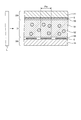
- FIG. 2 is a schematic cross-sectional view of the liquid crystal display panel.
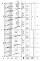
- FIG. 3 is a timing chart showing an example of the flow of field sequential control according to the first embodiment.
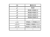
- FIG. 4 is a table diagram showing the components of the line image displayed and output in each pixel line during the frame period FL in the first embodiment.
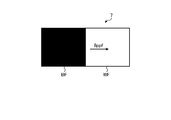
- FIG. 5 is an explanatory diagram of a test pattern relating to the occurrence of a color break.
- FIG. 6 is a chart showing an example of the relationship between the frame rate, the RGB light source lighting frequency, and the color break index.
- FIG. 7 is a table diagram showing the relationship between the luminance index for each mode and the lighting amount of the light source 11 in the first embodiment.
- FIG. 8 is a timing chart showing an example of the flow of field sequential control according to the second embodiment.
- FIG. 9 is a table diagram showing the relationship between the brightness index for each mode and the lighting amount of the light source 11 in the second embodiment.
- FIG. 10 is a timing chart showing an example of the flow of field sequential control according to the third embodiment.
- FIG. 11 is a timing chart showing an example of the flow of field sequential control according to the fourth embodiment.
- FIG. 12 is a timing chart showing an example of the flow of field sequential control according to the fourth embodiment.
- FIG. 13 is a table diagram showing the relationship between the brightness index for each mode and the lighting amount of the light source 11 in the fourth embodiment.
- FIG. 14 is a table diagram showing the relationship between the brightness index for each mode and the lighting amount of the light source 11 in the fourth embodiment.
- FIG. 15 is a timing chart showing an example of the flow of field sequential control including the three subframe periods.
- FIG. 1 is a schematic circuit diagram showing a main configuration of the display device 100.
- the display device 100 includes a liquid crystal display panel P and a light source device L.
- the liquid crystal display panel P includes a display unit 7, a signal output circuit 8, a scanning circuit 9, a VCOM drive circuit 10, a timing controller 13, and a power supply circuit 14.
- a display surface one side of the liquid crystal display panel P facing the display unit 7
- the other surface is referred to as a back surface.
- it is described as the side of the display device 100, it is located in a direction intersecting (for example, orthogonal to) the display surface and the back surface in the opposite direction with respect to the display device 100.
- a plurality of pixel Pix are arranged in a matrix on the display unit 7.
- the pixel Pix includes a switching element 1 and two electrodes.
- a pixel electrode 2 and a common electrode 6 are shown as two electrodes.
- FIG. 2 is a schematic cross-sectional view of the liquid crystal display panel P.
- the liquid crystal display panel P has two opposing substrates and a liquid crystal 3 enclosed between the two substrates.
- one of the two substrates will be referred to as a first substrate 30, and the other will be referred to as a second substrate 20.
- the first substrate 30 is an insulating glass substrate 35, a pixel electrode 2 laminated on the second substrate 20 side of the glass substrate 35, and an insulation laminated on the second substrate 20 side so as to cover the pixel electrode 2.
- the pixel electrode 2 is individually provided for each pixel Pix.
- the second substrate 20 includes a translucent glass substrate 21, a common electrode 6 laminated on the first substrate 30 side of the glass substrate 21, and an insulator laminated on the first substrate 30 side so as to cover the common electrode 6.
- the common electrode 6 has a plate-like or film-like shape shared by a plurality of pixels Pix.
- the liquid crystal 3 of the first embodiment is a polymer-dispersed liquid crystal. Specifically, the liquid crystal 3 contains a bulk 51 and fine particles 52. The orientation of the fine particles 52 changes in the bulk 51 according to the potential difference between the pixel electrode 2 and the common electrode 6. By individually controlling the potential of the pixel electrode 2 for each pixel Pix, at least one degree of light transmission or dispersion is controlled for each pixel Pix.
- the pixel electrode 2 and the common electrode 6 face each other so as to sandwich the liquid crystal 3, but the liquid crystal display panel P has the pixel electrode 2 and the common electrode 6 on one substrate.
- the orientation of the liquid crystal 3 may be controlled by the electric field generated by the pixel electrode 2 and the common electrode 6. Further, the liquid crystal 3 may be a liquid crystal other than the polymer dispersion type liquid crystal.
- the switching element 1 is a switching element using a semiconductor such as a thin film transistor (TFT).
- TFT thin film transistor
- One of the source and drain of the switching element 1 is connected to one of the two electrodes (pixel electrode 2).
- the other of the source or drain of the switching element 1 is connected to the signal line 4.
- the gate of the switching element 1 is connected to the scanning line 5.
- the scanning line 5 provides a potential for opening and closing between the source and drain of the switching element 1 under the control of the scanning circuit 9.
- the scanning circuit 9 controls the potential.
- the plurality of signal lines 4 are arranged along one of the arrangement directions of the pixels Pix (row direction).
- the signal line 4 extends along the other (column direction) of the arrangement directions of the pixels Pix.
- the signal line 4 is shared by the switching elements 1 of a plurality of pixels Pix arranged in the column direction.
- the plurality of scanning lines 5 are arranged along the column direction.
- the scanning line 5 extends along the row direction.
- the scanning line 5 is shared by the switching elements 1 of a plurality of pixels Pix arranged in the row direction.
- the common electrode 6 is connected to the VCOM drive circuit 10.
- the VCOM drive circuit 10 gives the common electrode 6 a potential that functions as a common potential.
- the signal output circuit 8 outputs a gradation signal described later to the signal line 4, so that the pixel electrode 2 and the common electrode 6 are used.
- the storage capacity formed between the two and the liquid crystal (fine particles 52), which is a capacitive load, is charged.
- the voltage of the pixel Pix becomes a voltage corresponding to the gradation signal.
- the liquid crystal (fine particles 52) which is the storage capacity and the capacitive load, retains the gradation signal.
- the orientation of the liquid crystal (fine particles 52) is controlled according to the electric field generated by the voltage of each pixel Pix and the voltage of the common electrode 6.
- a light source 11 is arranged on the side of the liquid crystal display panel P.
- the light source 11 includes a first light source 11R that emits red light, a second light source 11G that emits green light, and a third light source 11B that emits blue light.
- the first light source 11R, the second light source 11G, and the third light source 11B each emit light under the control of the light source drive circuit 12.
- the first light source 11R, the second light source 11G, and the third light source 11B of the first embodiment are light sources using a light emitting element such as a light emitting diode (LED: Light Emitting Diode), but are not limited thereto. Any light source may be used as long as the light emission timing can be controlled.
- the light source drive circuit 12 controls the light emission timings of the first light source 11R, the second light source 11G, and the third light source 11B under the control of the timing controller 13.
- the timing controller 13 controls the operation timing of the signal output circuit 8, the scanning circuit 9, the VCOM drive circuit 10, and the light source drive circuit 12. In the first embodiment, field sequential control is performed.
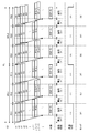
- FIG. 3 is a timing chart showing an example of the flow of field sequential control according to the first embodiment.
- FIG. 3 shows the relationship between the frame period FL, the subframe period (first subframe period SFL1, the second subframe period SFL2), and the field periods FI11, FI12, FI13, FI21, FI22, and FI23. Further, FIG. 3 shows the lighting timings, signal lines 4 and scanning lines of each of the light sources 11 (first light source 11R, second light source 11G and third light source 11B) of the field periods FI11, FI12, FI13, FI21, FI22 and FI23.
- a mode is shown in which the signal is controlled with respect to 5, the potential (common potential) given to the common electrode 6 by the VCOM drive circuit 10, and the potential difference (polarity) between the pixel electrode 2 and the common electrode 6 are determined.
- the one-frame period FL is shown as an example, but in reality, the same frame period FL is periodically repeated.
- the frame period FL is the period related to the display of the frame image.
- One frame image is displayed in one frame period FL.
- the one-frame period FL includes two subframe periods of the first subframe period SFL1 and the second subframe period SFL2.
- each subframe period includes a field period.
- FIG. 3 and the like three field periods FI11, FI12, and FI13 included in the first subframe period SFL1 and three field periods FI21, FI22, and FI23 included in the second subframe period SFL2 are illustrated.
- the number of field periods included in one subframe period corresponds to the number of colors of the light source 11.
- the number of colors of the light source 11 including the first light source 11R, the second light source 11G, and the third light source 11B is three. Therefore, the one subframe period of Embodiment 1 includes a three field period.
- the number of colors and the types of colors of the light source 11 and the number of field periods included in one subframe period in the first embodiment are merely examples and are not limited to these, and can be changed as appropriate.
- the display device 100 alternately generates a gradation signal writing period for a plurality of pixel Pix provided in the display unit 7 and a gradation signal holding period, and lights the light source 11 during the holding period. Display the image.
- a writing period it means a writing period of a gradation signal for a plurality of pixel Pix provided on the display unit 7.
- a retention period it refers to a writing period of gradation signals for a plurality of pixel Pix provided on the display unit 7.
- the TFT provided in the pixel Pix is turned on by the output of the drive signal to the scanning line 5 by the scanning circuit 9, and the gradation signal is output to the signal line 4 by the signal output circuit 8 to the pixel Pix.
- This is the period during which signal control for writing the tuning signal is performed.
- the holding period is a period in which all the TFTs are turned off and signal control for holding the voltage written in the writing period is performed.
- Each field period includes a write period and a retention period after the write period.
- the writing (R +) in FIG. 3 is the writing period of the field period FI11.
- Retention (R +) is the retention period of the field period FI11.
- the writing (G +) is the writing period of the field period FI12.
- Retention (G +) is the retention period of the field period FI12.
- the writing (B +) is the writing period of the field period FI13.
- Retention (B +) is the retention period of the field period FI13.
- the writing (R ⁇ ) is the writing period of the field period FI21.
- Retention (R-) is the retention period of the field period FI21.
- the writing (G ⁇ ) is the writing period of the field period FI22.
- Retention (G-) is the retention period of the field period FI22.
- Writing (B ⁇ ) is the writing period of the field period FI23.
- Retention (B-) is the retention period of the field period FI23.
- a time-division color display output method in which light sources of different colors (for example, the first light source 11R, the second light source 11G, and the third light source 11B) are turned on in each field period within one subframe period. : Field Sequential Color) is adopted.
- gradation signals corresponding to gradation values of different colors are written in each of the plurality of field periods included in one subframe period.
- a signal indicating the RGB gradation value assigned to one pixel Pix in one frame period a signal for each pixel Pix included in the input signal I (see FIG. 1) from the outside of the display device 100 is a pixel signal.
- (R, G, B) (r1, g1, b1) when the pixel signal is represented by RGB gradation values.
- r1 is a red (R) gradation value in the input signal including information indicating the RGB gradation value.
- g1 is a green (G) gradation value in the input signal including information indicating the RGB gradation value.
- b1 is a blue (B) gradation value in the input signal including information indicating the RGB gradation value.
- the gradation signal corresponding to the gradation value of "r1” is written in the writing period of the field period FI11. Further, a gradation signal corresponding to the gradation value of "g1" is written in the writing period of the field period FI12. Further, the gradation signal corresponding to the gradation value of "b1” is written in the writing period of the field period FI13.
- each field period the gradation signals corresponding to the gradation values of different colors written in the writing period in this way are retained.
- Writing and holding of the gradation signal in each of the field periods is performed individually for each of the plurality of pixel Pix.
- the FSC has been described above by taking the signal control during the first subframe period SFL1 as an example, the signal control of the field periods FI21, FI22, and FI23 during the second subframe period SFL2 is also described in the first subframe period SFL1. It is the same as the signal control of each of the field periods FI11, FI12, and FI13 in the middle.
- the light sources of a plurality of colors included in the light source 11 are controlled to be lit within the retention period of the corresponding field period.
- the first light source 11R is a red light source
- the second light source 11G is a green light source
- the third light source 11B is a blue light source.
- the lighting timing of the first light source 11R is indicated by “lighting (R)”.
- the lighting timing of the second light source 11G is indicated by “lighting (G)”.
- the lighting timing of the third light source 11B is indicated by “lighting (B)”. In this way, the image is displayed by turning on the light source 11 during the holding period. Therefore, the retention period functions as an image display period.
- an inversion drive is performed in which the relative potentials of one of the two electrodes and the other are inverted at a predetermined cycle.
- the relative height of the potential of the pixel electrode 2 due to the writing of the gradation signal performed during the writing period and the common potential, that is, the potential given to the common electrode 6 by the VCOM drive circuit 10 is added (+).
- a relatively high potential is a plus (+) and a relatively low potential is a minus ( ⁇ ).
- the common potential is minus (-).
- the writing period writing (R +), writing (G +), writing (B +)) and holding period (holding (R +), holding (G +)) of each field period in the first subframe period SFL1.
- Retention (B +)) is a plus (+) that is relatively high relative to the common potential of minus ( ⁇ ), which is indicated by the sign “+” in parentheses.
- the plus (+) and the minus ( ⁇ ) are reversed as compared with the first subframe period SFL1.
- the polarity of the electric field between the two substrates is reversed in the subframe period period.
- the first subframe period SFL1 is in the positive (P) mode and the second subframe period SFL2 is in the negative (N) mode, but the order may be reversed. Good. That is, the first subframe period SFL1 may be in the negative (N) mode and the second subframe period SFL2 may be in the positive (P) mode.
- the TFT provided in the pixel Pix is turned on by the output of the drive signal to the scanning line 5 by the scanning circuit 9, and the gradation signal to the signal line 4 by the signal output circuit 8 is turned on.
- Signal control is performed by the output to write a gradation signal to the pixel Pix. Therefore, the writing timings of the gradation signals for a plurality of Pix included in the pixel rows connected to the common scanning line 5 and simultaneously turned on in response to the driving signal for the scanning line 5 are simultaneous.
- the frame image is composed of a plurality of line images arranged along the alignment direction of the scanning lines 5.
- the plurality of pixel Pix connected to the common signal line 4 are connected to different scanning lines 5.
- the drive signal is connected to any of the plurality of scan lines 5 to which the drive signal is given at the same time, and is connected to the common signal line 4.
- the gradation signal given to the signal line 4 can be written to the plurality of pixels Pix at the same timing. Therefore, when a drive signal is given to a plurality of scanning lines 5 at the same timing and a line image is written in a plurality of pixel lines, each line image of the plurality of pixel lines written at one time is the same line. It becomes an image.
- the line image is an image displayed and output by a plurality of pixels Pix arranged along the extending direction of the scanning line 5 (the arranging direction of the signal lines 4).
- the display device 100 Based on the relationship between the signal line 4, the scanning line 5, and the pixel Pix described as described above, the display device 100 writes a line image in units of a predetermined number of lines during the writing period.
- the predetermined number of line images written at one time in units of a predetermined number of lines are the same line image. Further, the predetermined number is a natural number of 2 or more and corresponds to the number of subframes.
- a line image to be written in the writing period of the previous subframe period (first line image) and a line image to be written in the writing period of the later subframe period ( If it is different from the second line image)
- the start position of the writing period of the previous subframe period and the start position of the writing period of the subsequent subframe period are shifted by one line.
- the start position of writing a line image based on a different pixel signal is shifted by one line in each writing period of two consecutive subframe periods within one frame period.
- the relationship between the first line image and the second line image is, for example, a line image based on the same frame image but having different pixel row positions in the input signal I.
- the positional relationship of the pixel rows connected to the different scanning lines 5 is set to "y” and "numbers (1, 2, 3, 4, 5, ..., (L), (L), It is shown by a combination of "L + 1), (L + 2), ...)".
- the pixel line located on one end side of the scanning lines 5 in the alignment direction of the display unit 7 is defined as "y1". Therefore, it is assumed that the pixel rows are arranged in the order of y1, y2, y3, y4, y5, ..., Y (L), y (L + 1), y (L + 2) ....
- the scanning circuit 9 performs scanning by repeating the process of giving a driving signal to a part of a plurality of scanning lines 5 while switching the scanning line 5 to which the driving signal is given.
- the scanning circuit 9 of the first embodiment switches the scanning line 5 to which the drive signal is given from one end side to the other end side in the alignment direction of the scanning lines 5.
- gradation signals corresponding to gradation values of different colors are written in each of the plurality of field periods included in one subframe period.
- Y (L) a line image given to each pixel row of y1, y2, y3, y4, y5, ..., Y (L), y (L + 1), y (L + 2) ...
- the numbers corresponding to the positions of the plurality of line images constituting the input signal I are indicated by the numbers attached to the side (right side) of the code (R, G or B) indicating the color. ..
- the rectangle of "R1” is a line image in which the gradation value of red (R) among the line images given to the pixel line at the position of "y1" is reflected in the input signal I.
- the square of "G3” is a line image in which the gradation value of green (G) is reflected in the line image given to the pixel line at the position of "y3" in the input signal I. Shown.
- the square of "B (L)” reflects the gradation value of blue (B) in the line image given to the pixel line at the position of "y (L)" in the input signal I. Indicates that it is a line image.
- L of "number (1,2,3,4,5, ..., (L), (L + 1), (L + 2), ...)" is an odd number of 3 or more natural numbers.
- the line image is written in units of two lines during the writing period.
- the first line, the third line, ..., the (L) line, ... are given to the pixel lines.
- the line image is written in units of two adjacent lines.
- the second subframe period SFL2 among the plurality of line images included in the input signal I, the lines given to the pixel lines of the second line, the fourth line, ..., the (L + 1) line, ... Images are written in units of two adjacent lines.
- the start position of writing a line image based on a different pixel signal is shifted by one line in each writing period of the two subframe periods.
- the “line image based on different pixel signals” refers to line images having different positions in a plurality of line images included in the input signal I. That is, the relationship between the line image of the "first line” and the line image of the "second line” in the plurality of line images included in the input signal I is "a line image based on different pixel signals”.
- the "red (R), green (G), and blue (B) gradation values of the first line image correspond to the "red (R), green (G), and blue (B) gradation values of the first line image correspond to the "
- the line image reflecting "R1", “G1", and “B1” is the pixels of "y1" and "y2" during the writing period of the field periods FI11, FI12, and FI13 included in the first subframe period SFL1.
- "R3" and “G3” corresponding to the respective gradation values of red (R), green (G), and blue (B) of the line image of the third line.
- the writing position of the line image written in units of two lines in the writing period of the field periods FI21, FI22, and FI23 included in the second subframe period SFL2 is shifted by one line as compared with the first subframe period SFL1.
- the writing position of the line image that does not correspond to the "line image based on different pixel signals" is the same even in different subframe periods. Specifically, even during the writing period of the field periods FI21, FI22, and FI23 included in the second subframe period SFL2, the red (R), green (G), and blue (G) of the line image of the first line ( The line image reflecting "R1", “G1", and “B1" corresponding to each gradation value of B) is included in the second subframe period SFL2, and the writing period of the field periods FI21, FI22, and FI23. It is written in the pixel line of "y1".
- the components of the line image displayed and output in each pixel line are the component of the line image written in the first subframe period SFL1 and the line image written in the second subframe period SFL2. It is a combination of the components of.
- FIG. 4 is a table diagram showing the components of the line image displayed and output in each pixel line during the frame period FL in the first embodiment.
- the line images written at one time in a two-pixel line are the same line image.
- the pixel line of "y1" as described above, writing and display based on the line image based on the pixel signal at the position of "y1" common to both the first subframe period SFL1 and the second subframe period SFL2.
- Output is done. Therefore, the components of the line image displayed and output in the pixel line of "y1" are composed of "R1", “G1", and "B1" of each field period of the first subframe period SFL1 and the second subframe period SFL2. It is "RGB1".
- the line images written in the first subframe period SFL1 and the second subframe period SFL2 are different.
- writing and display output based on the line image based on the pixel signal at the position of "y1” are performed in the first subframe period SFL1.
- writing and display output based on the line image based on the pixel signal at the position of "y2” are performed in the second subframe period SFL2.
- the components of the line image displayed and output in the pixel line of "y2" are "RGB1" in which "R1", “G1", and “B1" of each field period of the first subframe period SFL1 are combined.
- Second subframe period The number of subframe periods (2 in the first embodiment) is the sum of the components obtained by adding "RGB2", which is a combination of “R2", “G2", and “B2" of each field period of SFL2. Divided "(RGB1 + RGB2) / 2".
- the components of the line image output by displaying the pixel lines other than the pixel lines of "y1" are the line images written in each field period of the first subframe period SFL1 by the same mechanism as the pixel lines of "y2" described above.
- the component obtained by adding the component of the above and the component of the line image written in each field period of the second subframe period SFL2 is divided by the number of subframe periods.
- the components of the line image displayed and output in the pixel line of "y (L)” are “R (L-1)” and “G (L-1)” of each field period of the first subframe period SFL1. , “RGB (L-1)” in which “B (L-1)” is synthesized, and “R (L)", “G (L)", “B” in each field period of the second subframe period SFL2.
- the components of the line image displayed and output in the pixel line of "y (L + 1)" are “R (L)", “G (L)", and “B (") of each field period of the first subframe period SFL1.
- "RGB (L)” in which "L)” was synthesized and “R (L + 1)", “G (L + 1)", and “B (L + 1)” in each field period of the second subframe period SFL2 were combined. It is " ⁇ RGB (L) + RGB (L + 1) ⁇ / 2" obtained by dividing the component obtained by adding "RGB (L + 1)” by the number of subframe periods (2 in the first embodiment).
- the components of the line image displayed and output in the pixel line of "y (L + 2)" are “R (L + 1)", “G (L + 1)", and “B (B)” of each field period of the first subframe period SFL1.
- "RGB (L + 1)” in which "L + 1)” was synthesized and "R (L + 2)", “G (L + 2)", and “B (L + 2)” in each field period of the second subframe period SFL2 were combined. It is " ⁇ RGB (L + 1) + RGB (L + 2) ⁇ / 2” obtained by dividing the component obtained by adding "RGB (L + 2)" by the number of subframe periods (2 in the first embodiment).
- the line image given to the pixel row of the (L) th row is the pixel row of the "y (L)" and has a 1/2 frame period.
- the display is output, and the pixel line of "y (L + 1)” is displayed and output for a 1/2 frame period, so that the display is output during one frame period.
- the line image given to the pixel line of the (L + 1) th line is the pixel line of "y (L + 1)" and is displayed and output for a 1/2 frame period.
- the pixel line of "y (L + 2)" is displayed and output for a half frame period, so that the display is output during one frame period.
- a predetermined number of line images written at one time in a predetermined number of line units are regarded as the same line image, and are based on different pixel signals in each writing period of two consecutive subframe periods within one frame period.
- FIG. 5 is an explanatory diagram of a test pattern relating to the occurrence of a color break.
- the display unit 7 performs a display output in which a region having the lowest light scattering degree (black region BF) and a region having the highest light scattering degree (white region WF) are adjacent to each other.
- the state of being is set as the start state. From this start state, control (8ppf: 8 pixel per frame) is applied to widen the black area BF toward the white area WF side by 8 pixels for each frame period FL and change the display output content so as to narrow the white area WF by that amount.
- control (8ppf: 8 pixel per frame) is applied to widen the black area BF toward the white area WF side by 8 pixels for each frame period FL and change the display output content so as to narrow the white area WF by that amount.
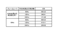
- FIG. 6 is a table diagram showing an example of the relationship between the frame rate, the RGB light source lighting frequency, and the color break index (CBI: Color Break Index).
- the frame rate is the number of frame period FLs per second.
- the RGB light source lighting frequency indicates the number of times that the lighting periods of the first light source 11R, the second light source 11G, and the third light source 11B included in the light source 11 make a round per second. Therefore, the number of lightings per second of each of the first light source 11R, the second light source 11G, and the third light source 11B included in the light source 11 is the same as the RGB light source lighting frequency.
- the value of the frequency at which the light source of any color included in the light source 11 is lit is the value obtained by multiplying the RGB light source lighting frequency by the number of colors (3).
- CBI is an index derived based on the calculation method for color break measurement proposed by SEMI (Semiconductor Equipment and Materials International). The smaller the CBI value, the more difficult it is to see the color break.
- the frame rate and the RGB light source lighting frequency are made the same as compared with the case where the RGB light source lighting frequency is further increased under the condition that the frame rate is fixed at 60 [Hz].
- the higher the RGB light source lighting frequency the better the CBI. Therefore, in the first embodiment, the frame rate and the RGB light source lighting frequency are the same, and the frame rate and the RGB light source lighting frequency are values exceeding 60 [Hz] (for example, 120 [Hz] or 240 [Hz]). It is said.
- the relationship between the frame rate and the RGB light source lighting frequency can be arbitrarily set by arbitrarily setting the frame rate and the RGB light source lighting frequency.
- the brightness of the display output content by the display unit 7 may differ.
- the reason why the brightness difference occurs between the positive (P) mode and the negative (N) mode is the potential given to the common electrode 6 by the VCOM drive circuit 10 in the positive (P) mode and the common electrode of the VCOM drive circuit 10 in the negative (N) mode. This is because it is technically difficult to set the intermediate potential with the potential given to 6 to 0 [V]. That is, the difference in brightness may occur due to the variation between the absolute value of the potential of each part in the positive (P) mode and the absolute value of the potential of each part in the negative (N) mode. Therefore, the lighting amount of the light source 11 in the positive (P) mode and the lighting amount of the light source 11 in the negative (N) mode may be different.
- FIG. 7 is a table diagram showing the relationship between the brightness index for each mode and the lighting amount of the light source 11 in the first embodiment.
- the brightness index is based on the brightness when a predetermined gradation value is given to all pixel Pix of the display unit 7 ( ⁇ 0), and the gradation value at which the brightness becomes the highest is given to all pixel Pix of the display unit 7. This is the brightness of the display unit 7 in the case.
- the display device 100 of the first embodiment is in the positive (P) mode in the first subframe period SFL1 and in the negative (N) mode in the second subframe period SFL2.
- the luminance index of the positive (P) mode of the display unit 7 is ⁇
- the luminance index of the negative (N) mode is ⁇ .
- the lighting amount ( ⁇ ) of the light source 11 in the positive (P) mode and the lighting amount ( ⁇ ) of the light source 11 in the negative (N) mode are different.
- ⁇ and ⁇ for example, when a gradation value that maximizes the brightness is given to all the pixels Pix of the display unit 7, the brightness of the display unit 7 is in the positive (P) mode and the negative (N) mode. Is set to be substantially the same.
- the display device 100 using the polymer-dispersed liquid crystal described with reference to FIGS. 1 and 2 tends to have ⁇ > ⁇ . Therefore, for example, when the potential given to the common electrode 6 by the VCOM drive circuit 10 in the positive (P) mode described above and the potential given to the common electrode 6 by the VCOM drive circuit 10 in the negative (N) mode are different from each other, and ⁇ > ⁇ . , ⁇ ⁇ , but the relationship between ⁇ and ⁇ and the relationship between ⁇ and ⁇ are not limited to this, and both may be reversed.
- the relationship between ⁇ and ⁇ according to the relationship between ⁇ and ⁇ , the difference in brightness between the positive (P) mode and the negative (N) mode can be suppressed.
- ⁇ ⁇
- the input circuit 15 controls the output of the line image written during the writing period.
- the input circuit 15 outputs a gradation signal indicating the gradation value of each of the red (R), green (G), and blue (B) colors of each pixel Pix to the signal output circuit 8 based on the input signal I. ..
- the input circuit 15 outputs a synchronization signal and other control signals synchronized with the input timing of the gradation signal to the signal output circuit 8 to the timing controller 13.
- the timing controller 13 controls the operations of the signal output circuit 8, the scanning circuit 9, the VCOM drive circuit 10, and the like based on the signal input from the input circuit 15.
- the input circuit 15 of the first embodiment is, for example, an FPGA (Field Programmable Gate Array) mounted on a flexible printed circuit board (not shown) connected to the liquid crystal display panel P or a circuit capable of realizing the same function.
- the input circuit 15 includes a memory 15a for holding frame image data.
- the input circuit 15 outputs a line image from the frame image stored in the memory 15a in the writing period of each field period in units of line images as described with reference to FIG. 3, for example.
- the memory 15a may have a storage capacity capable of outputting line images in the order as described with reference to FIG. 3, for example.
- the input circuit 15 outputs the previously input frame images of one frame in line image units and the line. It is possible to retain a frame image for one frame after being input in parallel during the image output period.
- the display device 100 includes a liquid crystal display panel P in which a liquid crystal 3 is enclosed between two opposing substrates and a plurality of line images are arranged in a scanning direction to display a frame image, and a liquid crystal.
- the display panel P is provided with a light source 11 for irradiating light.
- the one-frame period FL assigned to one frame image includes a predetermined number (for example, 2) of subframe periods.
- the subframe period includes a line image writing period and a display period in which light from the light source 11 is irradiated. During the writing period, line images are written in units of a predetermined number of lines.
- the predetermined number of line images written at one time in units of a predetermined number of lines are the same line image.
- the previous sub The start position of the writing period of the frame period and the start position of the writing period of the subframe period after that are shifted by one line.
- the number of times the scanning circuit 9 switches the scanning line 5 for outputting the drive signal in one writing period as compared with the case where different line images are sequentially written in the scanning direction for each pixel line in the writing period. Can be reduced. Therefore, the time allocated to one writing period can be shortened. Further, by providing a predetermined number of subframe periods in one frame period and making the start position of writing the line image different from the line image to be written in each subframe period, the display output of the frame image in one frame period unit is performed. It is possible to achieve both substantial maintenance of the content and an increase in the frame rate by providing a subframe period. That is, the frame rate can be further increased while substantially maintaining the display output content by the predetermined number of subframe periods and the shift of the line image. Therefore, according to the first embodiment, the frame rate can be further increased, so that the color break can be suppressed.
- the later subframe period (for example, the second subframe period SFL2) of the two consecutive subframe periods within the one frame period is in the scanning direction from the start position of writing the line image based on the different pixel signals.
- the line image located on the upstream side is the same line image as the line image written in the previous subframe period (for example, the first subframe period SFL1) of the two subframe periods.
- the light source 11 includes a light source of a plurality of colors whose lighting period can be individually controlled (for example, a first light source 11R, a second light source 11G, and a third light source 11B).
- the subframe period includes a plurality of field periods provided for each of the plurality of colors.
- the one-field period includes a writing period and a display period.
- the polarity of the electric field between the two substrates is reversed in a predetermined period (for example, a subframe period) cycle. As a result, deterioration of the liquid crystal 3 can be suppressed.
- the brightness of the image visually recognized can be made more uniform even when the brightness index is different due to the difference in the mode.
- FIG. 8 is a timing chart showing an example of the flow of field sequential control according to the second embodiment.
- the polarity of the electric field between the two substrates is reversed in the field period period. That is, in the second embodiment, the positive (P) mode and the negative (N) mode are switched in the field period cycle.
- the positive (P) mode and the negative (N) mode are switched between the field period FI11 and the field period FI12. Further, the negative (N) mode and the positive (P) mode are switched between the field period FI12 and the field period FI13. Further, the positive (P) mode and the negative (N) mode are switched between the field period FI13 and the field period FI21 that are continuous with the switching timing between the first subframe period SFL1 and the second subframe period SFL2 in between. Further, the negative (N) mode and the positive (P) mode are switched between the field period FI21 and the field period FI22.
- the positive (P) mode and the negative (N) mode are switched between the field period FI22 and the field period FI23.
- the two-field period that is continuous with the switching timing of the continuous two-frame period FL the two-field period that is continuous with the switching timing between the first subframe period SFL1 and the second subframe period SFL2 (for example). It is the same as the field period FI13 and the field period FI21).
- the first field period of the frame period FL starts from the positive (P) mode, but it may be reversed. That is, the first field period of the frame period FL may start from the negative (N) mode.
- FIG. 9 is a table diagram showing the relationship between the brightness index for each mode and the lighting amount of the light source 11 in the second embodiment.
- the relationship between the mode, the brightness index, and the lighting amount of the light source changes from the subframe period unit to the field period unit.
- the field period FI11, the field period FI13, and the field period FI22 are set to the positive (P) mode
- the field period FI12, the field period FI21, and the field period FI23 are set to the negative (N) mode.
- the relationship between the mode, the luminance index, and the lighting amount of the light source in the second embodiment is the same as that in the first embodiment, except for the difference between the period of the positive (P) mode and the period of the negative (N) mode.
- the second embodiment is the same as the first embodiment, except for the matters noted above.
- the polarity of the electric field between the two substrates (for example, the first substrate 30 and the second substrate 20) is reversed in the field period period.
- deterioration of the liquid crystal 3 can be suppressed.
- the amount of lighting of the light source 11 differs before and after the reversal of polarity. For example, when the degree of light scattering in one of the two consecutive field periods (for example, positive (P) mode) is stronger than that in the other, the lighting amount of one light source 11 is weaker than that in the other. As a result, the brightness of the image visually recognized can be made more uniform even when the brightness index differs depending on the mode.
- P positive
- FIG. 10 is a timing chart showing an example of the flow of field sequential control according to the third embodiment.
- the writing of the previous field period is described.
- the start position of the inclusion period and the start position of the writing period of the field period after that are shifted by one line. That is, the start position of writing a line image based on a different pixel signal is shifted by one line in each writing period of two consecutive field periods.
- the gradation value of red (R) of the line image of the first line is set.
- a line image reflecting the corresponding "R1” is written for the pixel lines of "y1" and "y2".
- a line image reflecting "R3" corresponding to the red (R) gradation value of the line image on the third line is written for the pixel lines of "y3" and "y4".
- the line image reflecting "R (L)” corresponding to the gradation value of red (R) of the line image on the (L) line by the same mechanism is "y (L)" and "y (L + 1)". ) ”Written to the pixel line.
- the third embodiment is the same as the first and second embodiments.
- a line image reflecting "G1" corresponding to the adjustment price is written for "y1".
- the line images reflecting "G2" corresponding to the gradation value of green (G) of the second line image are "y2" and "y3".
- a line image reflecting "G4" corresponding to the gradation value of green (G) of the line image on the fourth line is written for the pixel lines of "y4" and "y5".
- the line image reflecting "G (L + 1)" corresponding to the gradation value of green (G) of the line image on the (L + 1) line by the same mechanism is "y (L + 1)" and "y (L + 2)". ) ”Is written for the pixel line.
- the start position of writing the line image based on the different pixel signals is shifted by one line in each writing period of the two consecutive field periods (for example, the field period FI11 and the field period FI12).
- a line image reflecting "B1" corresponding to the adjustment price is written for the pixel lines of "y1" and "y2".
- a line image reflecting "B3" corresponding to the blue (B) gradation value of the line image on the third line is written for the pixel lines of "y3" and "y4".
- the line image reflecting "B (L)” corresponding to the gradation value of blue (B) of the line image on the (L) line by the same mechanism is "y (L)" and "y (L + 1)".
- the third embodiment is the same as the first and second embodiments as a result, but each writing of two consecutive field periods (for example, the field period FI12 and the field period FI13) is written.
- the start position of writing a line image based on different pixel signals in different periods is shifted by one line.
- a line image reflecting "R1" corresponding to the adjustment price is written for "y1".
- the line images reflecting "R2" corresponding to the red (R) gradation value of the second line image are "y2" and "y3".
- a line image reflecting "R4" corresponding to the red (R) gradation value of the line image on the fourth line is written for the pixel lines of "y4" and "y5".
- the line image reflecting "R (L + 1)" corresponding to the gradation value of red (R) of the line image on the (L + 1) line by the same mechanism is "y (L + 1)" and "y (L + 2)”.
- ) Written to the pixel line.
- the third embodiment is the same as that of the first and second embodiments as a result, but the two continuous field periods (for example, the field) with the switching timing of the two consecutive subframe periods in between. The start position of writing a line image based on a different pixel signal is shifted by one line in each writing period of the period FI13 and the field period FI21).
- a line image reflecting "G1" corresponding to the adjustment price is written for the pixel lines of "y1" and "y2".
- a line image reflecting "G3" corresponding to the gradation value of green (G) of the line image on the third line is written for the pixel lines of "y3" and "y4".
- the line image reflecting "G (L)” corresponding to the gradation value of green (G) of the line image on the (L) line by the same mechanism is "y (L)" and "y (L + 1)".
- the start position of writing the line image based on the different pixel signals is shifted by one line in each writing period of the two consecutive field periods (for example, the field period FI21 and the field period FI22).
- a line image reflecting "B1" corresponding to the adjustment price is written for "y1".
- the line images reflecting "B2" corresponding to the blue (B) gradation value of the second line image are "y2" and "y3".
- a line image reflecting "B4" corresponding to the blue (B) gradation value of the line image on the fourth line is written for the pixel lines of "y4" and "y5".
- the line image reflecting "B (L + 1)" corresponding to the gradation value of blue (B) of the line image on the (L + 1) line by the same mechanism is "y (L + 1)" and "y (L + 2)". ) ”Is written for the pixel line.
- the third embodiment is the same as the first and second embodiments as a result, but each writing of two consecutive field periods (for example, the field period FI22 and the field period FI23) is written. The start position of writing a line image based on different pixel signals in different periods is shifted by one line.
- the third embodiment is the same as the second embodiment except for the matters noted above.
- the previous line image is written.
- the start position of the writing period of the field period and the start position of the writing period of the field period after that are shifted by one line.
- the start position of writing a line image based on a different pixel signal is shifted by one line in each writing period of two consecutive field periods, and two substrates (for example, the first substrate 30 and the second substrate 30) are shifted in the field period period.
- the polarity of the electric field between the substrates 20) is reversed.
- the line image located at the odd-numbered position in the scanning direction and the line image located at the even-numbered position in the input signal I can be dispersed over a plurality of subframe periods. Therefore, even if a so-called stripe pattern in which the brightness difference between the odd-numbered line image and the even-numbered line image is remarkable is input, the brightness difference of the line image is reflected in the subframe period unit. Can be suppressed.
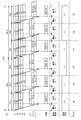
- FIGS. 11 and 12 are timing charts showing an example of the flow of field sequential control according to the fourth embodiment.
- FIGS. 11 and 12 are timing charts showing an example of the flow of field sequential control according to the fourth embodiment.
- FIGS. 11 and 12 are shown in FIGS. 11 and 12.
- FIG. 11 shows the first frame period FL1 of the two consecutive frame period FLs.
- FIG. 12 shows the second frame period FL2 after the continuous two frame period FL. After the second frame period FL2, the first frame period FL1 continues again.
- the polarity of the electric field between the two substrates is reversed in a two-field period period. That is, in the fourth embodiment, the positive (P) mode and the negative (N) mode are switched in a two-field period cycle.
- the positive (P) mode is continuous between the field period FI11 and the field period FI12 of the first frame period FL1 of the continuous two frame period FL, and the field period FI12
- the positive (P) mode and the negative (N) mode are switched between the field period FI13.
- the negative (N) mode is performed in two consecutive field periods (for example, field period FI13 and field period FI21) with a switching timing between the first subframe period SFL1 and the second subframe period SFL2 of the first frame period FL1. Is continuous, and the negative (N) mode and the positive (P) mode are switched between the field period FI21 and the field period FI22.
- the positive (P) mode is continuous in the field period FI22 and the field period FI23) of the first frame period FL1.
- the field period FI23 and the field period FI11 that are continuous with the switching timing of the continuous two-frame period FL are interposed.
- the positive (P) mode and the negative (N) mode are switched.
- the negative (N) mode is continuous between the field period FI11 and the field period FI12 of the second frame period FL2
- the negative (N) mode and the positive (N) mode and the positive (N) mode are formed between the field period FI12 and the field period FI13.
- P) The mode is switched.
- the positive (P) mode is performed in two consecutive field periods (for example, field period FI13 and field period FI21) with a switching timing between the first subframe period SFL1 and the second subframe period SFL2 of the second frame period FL2. Is continuous, and the positive (P) mode and the negative (N) mode are switched between the field period FI21 and the field period FI22. Further, the negative (N) mode is continuous in the field period FI22 and the field period FI23) of the first frame period FL1. After that, the negative (N) mode and the positive (P) are set in the continuous field period FI23 and the field period FI11 with the switching timing of the continuous two frame period FL (for example, the second frame period FL2 and the first frame period FL1) in between. The mode is switched.
- FIGS. 13 and 14 are charts showing the relationship between the brightness index for each mode and the lighting amount of the light source 11 in the fourth embodiment.
- the relationship between the mode, the luminance index, and the lighting amount of the light source is in units of two field periods.
- the field period FI11 of the first frame period FL1 the field period FI12, the field period FI22 and the field period FI23, and the field period FI13 and the field period FI21 of the second frame period FL2 are positive ( P) Mode is set.
- the field period FI13 and the field period FI21 of the first frame period FL1 and the field period FI11, the field period FI12, the field period FI22, and the field period FI23 of the second frame period FL2 are set to the negative (N) mode. Except for the difference between the period of the positive (P) mode and the period of the negative (N) mode, the relationship between the mode, the luminance index, and the lighting amount of the light source in the fourth embodiment is the same as that of the first embodiment.
- the fourth embodiment is the same as the third embodiment, except for the matters noted above.
- the start position of writing a line image based on a different pixel signal is shifted by one line in each writing period of two consecutive field periods, and two substrates (for example, two substrates in a two-field period period).
- the polarity of the electric field between the first substrate 30 and the second substrate 20) is reversed.
- the line image located at the odd-numbered position in the scanning direction and the line image located at the even-numbered position in the input signal I can be dispersed over a plurality of subframe periods. Therefore, even if a so-called stripe pattern in which the brightness difference between the odd-numbered line image and the even-numbered line image is remarkable is input, the brightness difference of the line image is reflected in the subframe period unit. Can be suppressed.
- the number of subframe periods is not limited to 2, and may be 3 or more. Good.
- FIG. 15 is a timing chart showing an example of the flow of field sequential control including a three-subframe period.
- the color distinction of the line image is omitted, and "D" and "number (1, 2, 3, 4, 5, ..., (L), (L + 1), (L + 2)" in the rectangle are omitted. , ...) ”is shown in combination.
- the number of colors of the light source 11 is 2 or more, that is, when a line image of a plurality of colors is written, a line is lined in each field period within each subfield period as in the case described with reference to FIG.
- the image is updated. For example, in the case of three colors of RGB, writing is performed in units of three lines of RGB for each subframe period.
- a line image is written in units of 3 lines during the writing period.
- the first subframe period SFL1 of the plurality of line images included in the input signal I, two lines in between, such as the first line, the fourth line, ..., the (L) line, ...
- the line image given to the pixel lines having a cycle of 3 lines is written in units of 3 lines.
- two lines between the plurality of line images included in the input signal I are skipped, such as the second line, the fifth line, ..., the (L + 1) line, ...
- a line image given to a pixel line having a three-line cycle is written in units of three lines.
- the third subframe period SFL3 two lines are skipped between the plurality of line images included in the input signal I, such as the third line, the sixth line, ..., the (L + 2) line, and so on.
- a line image given to a pixel line having a three-line cycle is written in units of three lines. In this way, the start position of writing a line image based on a different pixel signal in each writing period of the three subframe periods is shifted by one line before and after the continuous subframe period.
- the writing position of the line image that does not correspond to the "line image based on different pixel signals" is the same even in different subframe periods. Specifically, even during the writing period of the second subframe period SFL2 and the third subframe period SFL3, the line image reflecting "D1" in the first line is referred to as the first subframe period SFL1. The data will be similar. Further, even during the writing period of the third subframe period SFL3, the line image reflecting the “D2” in the second line has the same data as the second subframe period SFL2.
- the writing of "D2" on the first line during the inclusion period can be omitted.
- the number of colors of the light source 11 is 1, the number of field periods included in one subframe period is also 1. Therefore, it is not necessary to update the line image according to the color change within the subframe period, and it is not necessary to update the gradation signal for the pixel line in which the line image does not change across the continuous subframe period. Is.
- n is a natural number of 2 or more. Even in that case, the start position of writing the line image is shifted by one line before and after the two writing periods that occur with the continuous subframe period or the field period in between.
- the combination of light sources having a plurality of colors of the light source 11 is not limited to the combination of red (R), green (G), and blue (B).
- the light source 11 may have a light source corresponding to each of the three colors in combination with cyan, magenta, and yellow.
- the light source device L may illuminate the liquid crystal display panel P, and its specific arrangement can be changed as appropriate.
- the light source device L may be a front light.
- the liquid crystal display panel P is not limited to a liquid crystal display panel using a polymer-dispersed liquid crystal, and has other forms such as a transmissive type, transflective type or reflective type display panel to which FSC can be applied. It may be a display panel of. In the case of a transmissive display panel, the light source device L is provided on the back side of the display surface.
- Switching element 2 Pixel electrode 3 Liquid crystal 4 Signal line 5 Scan line 52 Fine particles 6 Common electrode 7
- Display unit 8 Signal output circuit 9
- VCOM drive circuit 11 Light source 11R 1st light source 11G 2nd light source 11B 3rd light source 12
- Light source drive Circuit 13 Timing controller 14 Power supply circuit 15
- Memory 100 Display device P Liquid crystal display panel L Light source device
Landscapes
- Physics & Mathematics (AREA)
- Engineering & Computer Science (AREA)
- General Physics & Mathematics (AREA)
- Theoretical Computer Science (AREA)
- Computer Hardware Design (AREA)
- Crystallography & Structural Chemistry (AREA)
- Chemical & Material Sciences (AREA)
- Nonlinear Science (AREA)
- Mathematical Physics (AREA)
- Optics & Photonics (AREA)
- Liquid Crystal Display Device Control (AREA)
- Control Of Indicators Other Than Cathode Ray Tubes (AREA)
- Liquid Crystal (AREA)
Abstract
表示装置は、対向する2枚の基板の間に液晶が封入され、複数のライン画像を走査方向に並べてフレーム画像を表示させる表示パネルと、表示パネルに光を照射する光源とを備え、1つのフレーム画像に対して割り当てられる1フレーム期間は、2以上の自然数である所定数のサブフレーム期間を含み、サブフレーム期間は、ライン画像の書込期間と光源からの光が照射される表示期間とを含み、書込期間に所定数ライン単位でライン画像が書き込まれ、所定数ライン単位で1度に書き込まれるライン画像は同一のライン画像であり、1フレーム期間内で連続する2サブフレーム期間において、前のサブフレーム期間の書込期間に書き込むライン画像と、後のサブフレーム期間の書込期間に書き込むライン画像とが異なる場合、当該前のサブフレーム期間の書込期間の開始位置と当該後のサブフレーム期間の書込期間の開始位置とが1ラインずれる。
Description
本発明は、表示装置に関する。
同一画素から複数色の光をそれぞれ異なるタイミングで透過させるように画素を制御する(フィールドシーケンシャル)液晶表示装置が知られている(例えば、特許文献1)。
フィールドシーケンシャルの表示装置において、ヒトの視認能力に対してフレームレートが低いと、カラーブレークと呼ばれる本来ならば意図しない色の変化が視認されることがある。
本発明は、上記の課題に鑑みてなされたもので、カラーブレークを抑制可能な表示装置を提供することを目的とする。
本発明の一態様による表示装置は、対向する2枚の基板の間に液晶が封入され、複数のライン画像を走査方向に並べてフレーム画像を表示させる表示パネルと、前記表示パネルに光を照射する光源とを備え、1つの前記フレーム画像に対して割り当てられる1フレーム期間は、2以上の自然数である所定数のサブフレーム期間を含み、前記サブフレーム期間は、前記ライン画像の書込期間と前記光源からの光が照射される表示期間とを含み、前記書込期間に前記所定数ライン単位で前記ライン画像が書き込まれ、前記所定数ライン単位で1度に書き込まれるライン画像は同一のライン画像であり、前記1フレーム期間内で連続する2サブフレーム期間において、前のサブフレーム期間の前記書込期間に書き込むライン画像と、後のサブフレーム期間の前記書込期間に書き込むライン画像とが異なる場合、当該前のサブフレーム期間の前記書込期間の開始位置と当該後のサブフレーム期間の前記書込期間の開始位置とが1ラインずれる。
本発明の一態様による表示装置は、対向する2枚の基板の間に液晶が封入され、複数のライン画像を走査方向に並べてフレーム画像を表示させる表示パネルと、前記表示パネルに光を照射する光源とを備え、1つの前記フレーム画像に対して割り当てられる1フレーム期間は、2以上の自然数である所定数のサブフレーム期間を含み、前記光源は、個別に点灯期間を制御可能な複数の色の光源を含み、前記サブフレーム期間は、前記複数の色毎に設けられた複数のフィールド期間を含み、1フィールド期間は、前記ライン画像の書込期間と前記光源からの光が照射される表示期間とを含み、前記書込期間に前記所定数ライン単位で前記ライン画像が書き込まれ、前記所定数ライン単位で1度に書き込まれるライン画像は同一のライン画像であり、連続する2フィールド期間において、前のフィールド期間の前記書込期間に書き込むライン画像と、後のフィールド期間の前記書込期間に書き込むライン画像とが異なる場合、当該前のフィールド期間の前記書込期間の開始位置と当該後のフィールド期間の前記書込期間の開始位置とが1ラインずれ、前記フィールド期間周期で前記2枚の基板間の電界の極性が反転する。
本発明の一態様による表示装置は、対向する2枚の基板の間に液晶が封入され、複数のライン画像を走査方向に並べてフレーム画像を表示させる表示パネルと、前記表示パネルに光を照射する光源とを備え、1つの前記フレーム画像に対して割り当てられる1フレーム期間は、2以上の自然数である所定数のサブフレーム期間を含み、前記光源は、個別に点灯期間を制御可能な複数の色の光源を含み、前記サブフレーム期間は、前記複数の色毎に設けられた複数のフィールド期間を含み、1フィールド期間は、前記ライン画像の書込期間と前記光源からの光が照射される表示期間とを含み、前記書込期間に前記所定数ライン単位で前記ライン画像が書き込まれ、前記所定数ライン単位で1度に書き込まれるライン画像は同一のライン画像であり、連続する2フィールド期間において、前のフィールド期間の前記書込期間に書き込むライン画像と、後のフィールド期間の前記書込期間に書き込むライン画像とが異なる場合、当該前のフィールド期間の前記書込期間の開始位置と当該後のフィールド期間の前記書込期間の開始位置とが1ラインずれ、2フィールド期間周期で前記2枚の基板間の電界の極性が反転する。
以下に、本発明の各実施の形態について、図面を参照しつつ説明する。なお、開示はあくまで一例にすぎず、当業者において、発明の主旨を保っての適宜変更について容易に想到し得るものについては、当然に本発明の範囲に含有されるものである。また、図面は説明をより明確にするため、実際の態様に比べ、各部の幅、厚さ、形状等について模式的に表される場合があるが、あくまで一例であって、本発明の解釈を限定するものではない。また、本明細書と各図において、既出の図に関して前述したものと同様の要素には、同一の符号を付して、詳細な説明を適宜省略することがある。
(実施形態1)
図1は、表示装置100の主要構成を示す模式的な回路図である。表示装置100は、液晶表示パネルPと、光源装置Lとを備える。液晶表示パネルPは、表示部7と、信号出力回路8と、走査回路9と、VCOM駆動回路10と、タイミングコントローラ13と、電源回路14とを備える。以下、表示部7が面する液晶表示パネルPの一面を表示面とし、他面を背面とする。また、表示装置100の側方と記載した場合、表示装置100を基準として表示面と背面との対向方向に交差(例えば、直交)する方向に位置する。
図1は、表示装置100の主要構成を示す模式的な回路図である。表示装置100は、液晶表示パネルPと、光源装置Lとを備える。液晶表示パネルPは、表示部7と、信号出力回路8と、走査回路9と、VCOM駆動回路10と、タイミングコントローラ13と、電源回路14とを備える。以下、表示部7が面する液晶表示パネルPの一面を表示面とし、他面を背面とする。また、表示装置100の側方と記載した場合、表示装置100を基準として表示面と背面との対向方向に交差(例えば、直交)する方向に位置する。
表示部7には、複数の画素Pixがマトリクス状に配置されている。画素Pixは、スイッチング素子1と、2つの電極とを含む。図1及び後述する図2では、2つの電極として、画素電極2と、共通電極6とを図示している。
図2は、液晶表示パネルPの概略断面図である。液晶表示パネルPは、対向する2枚の基板と、当該2枚の基板の間に封入された液晶3を有する。以下、当該2枚の基板の一方を第1基板30とし、他方を第2基板20とする。
第1基板30は、透光性のガラス基板35と、ガラス基板35の第2基板20側に積層された画素電極2と、画素電極2を覆うように第2基板20側に積層された絶縁層55とを含む。画素電極2は、画素Pix毎に個別に設けられる。第2基板20は、透光性のガラス基板21と、ガラス基板21の第1基板30側に積層された共通電極6と、共通電極6を覆うように第1基板30側に積層された絶縁層56とを含む。共通電極6は、複数の画素Pixで共有される板状又は膜状の形状を有する。
実施形態1の液晶3は、高分子分散型液晶である。具体的には、液晶3は、バルク51と、微粒子52とを含む。微粒子52は、バルク51内で画素電極2と共通電極6との電位差に応じて配向が変化する。画素Pix毎に画素電極2の電位が個別に制御されることで、画素Pix毎に少なくとも透光及び分散のいずれかの度合いが制御される。
図2を参照して説明した実施形態1では、画素電極2と共通電極6は、液晶3を挟むように対向するが、液晶表示パネルPは、1つの基板に画素電極2と共通電極6が設けられて画素電極2と共通電極6によって発生する電界によって液晶3の配向が制御される構成であってもよい。また、液晶3は高分子分散型液晶以外の液晶でもよい。
次に、画素電極2及び共通電極6の電位を制御する仕組みについて説明する。図1に示すようにスイッチング素子1は、例えば薄膜トランジスタ(TFT:Thin Film Transistor)等、半導体を用いたスイッチング素子である。スイッチング素子1のソース又はドレインの一方は、2つの電極の一方(画素電極2)と接続される。スイッチング素子1のソース又はドレインの他方が信号線4と接続される。スイッチング素子1のゲートは、走査線5と接続される。走査線5は、走査回路9の制御下で、スイッチング素子1のソース-ドレイン間を開閉するための電位を与える。当該電位の制御は、走査回路9が行う。
図1に示す例では、複数の信号線4は、画素Pixの並び方向のうち一方(行方向)に沿って並ぶ。信号線4は、画素Pixの並び方向のうち他方(列方向)に沿って延出する。信号線4は、列方向に並ぶ複数の画素Pixのスイッチング素子1で共有される。複数の走査線5は、列方向に沿って並ぶ。走査線5は、行方向に沿って延出する。走査線5は、行方向に並ぶ複数の画素Pixのスイッチング素子1で共有される。
共通電極6は、VCOM駆動回路10と接続される。VCOM駆動回路10は、共通電極6に共通電位として機能する電位を与える。走査回路9が走査線5に対して駆動信号として機能する電位を与えるタイミングで、信号出力回路8が信号線4に対して後述する階調信号を出力することで、画素電極2と共通電極6との間に形成された蓄積容量と容量性負荷である液晶(微粒子52)を充電する。これによって、画素Pixの電圧は階調信号に対応した電圧となる。駆動信号が与えられなくなった後、蓄積容量と容量性負荷である液晶(微粒子52)は階調信号を保持する。液晶(微粒子52)の配向は、各画素Pixの電圧と共通電極6の電圧によって生じる電界に応じて制御される。
図2に示すように、液晶表示パネルPの側方には、光源11が配置されている。光源11は、赤色の光を発する第1光源11Rと、緑色の光を発する第2光源11Gと、青色の光を発する第3光源11Bと、を有する。第1光源11R、第2光源11G、第3光源11Bはそれぞれ、光源駆動回路12の制御下で発光する。実施形態1の第1光源11R、第2光源11G及び第3光源11Bは、例えば発光ダイオード(LED:Light Emitting Diode)のような発光素子を用いた光源であるが、これに限られるものでなく、発光タイミングを制御可能な光源であればよい。光源駆動回路12は、タイミングコントローラ13の制御下で第1光源11R、第2光源11G、第3光源11Bの発光タイミングを制御する。
タイミングコントローラ13は、信号出力回路8、走査回路9、VCOM駆動回路10及び光源駆動回路12の動作タイミングを制御する。実施形態1では、フィールドシーケンシャル制御が行われる。
図3は、実施形態1のフィールドシーケンシャル制御の流れの一例を示すタイミングチャートである。図3は、フレーム期間FLとサブフレーム期間(第1サブフレーム期間SFL1、第2サブフレーム期間SFL2)とフィールド期間FI11,FI12,FI13,FI21,FI22,FI23との関係を示している。また、図3は、フィールド期間FI11,FI12,FI13,FI21,FI22,FI23の各々の光源11(第1光源11R、第2光源11G及び第3光源11B)の点灯タイミング、信号線4及び走査線5に対する信号制御、VCOM駆動回路10によって共通電極6に与えられる電位(共通電位)及び画素電極2と共通電極6との電位差(極性)に応じて決定するモードを示している。図3等のタイミングチャートでは、1フレーム期間FLを例示的に示しているが、実際には同様のフレーム期間FLが周期的に繰り返される。
フレーム期間FLは、フレーム画像の表示に係る期間である。1フレーム期間FLに、1つのフレーム画像が表示される。実施形態1では、1フレーム期間FLに、第1サブフレーム期間SFL1と第2サブフレーム期間SFL2の2サブフレーム期間が含まれる。
実施形態1では、各サブフレーム期間は、フィールド期間を含む。図3等では、第1サブフレーム期間SFL1に含まれる3つのフィールド期間FI11,FI12,FI13と、第2サブフレーム期間SFL2に含まれる3つのフィールド期間FI21,FI22,FI23とを例示している。
1サブフレーム期間に含まれるフィールド期間の数は、光源11の色数に対応する。実施形態1では、第1光源11R、第2光源11G及び第3光源11Bを含む光源11の色数が3である。従って、実施形態1の1サブフレーム期間は、3フィールド期間を含む。実施形態1における光源11の色数ならびに色の種類及び1サブフレーム期間に含まれるフィールド期間の数はあくまで一例であってこれに限られるものでなく、適宜変更可能である。
表示装置100は、表示部7に設けられた複数の画素Pixに対する階調信号の書込期間と、階調信号の保持期間とを交互に生じさせ、当該保持期間に光源11を点灯させることで画像を表示する。以下、単に書込期間と記載した場合、表示部7に設けられた複数の画素Pixに対する階調信号の書込期間をさす。また、単に保持期間と記載した場合、表示部7に設けられた複数の画素Pixに対する階調信号の書込期間をさす。
書込期間は、走査回路9による走査線5への駆動信号の出力によって画素Pixに設けられたTFTをオンさせるとともに信号出力回路8による信号線4への階調信号の出力によって画素Pixに階調信号を書き込む信号制御が行われる期間である。保持期間は、TFTが全てオフし、書込期間に書き込まれた電圧を保持する信号制御が行われる期間である。各フィールド期間は、書込期間と、書込期間後の保持期間とを含む。
図3における書込(R+)は、フィールド期間FI11の書込期間である。保持(R+)は、フィールド期間FI11の保持期間である。書込(G+)は、フィールド期間FI12の書込期間である。保持(G+)は、フィールド期間FI12の保持期間である。書込(B+)は、フィールド期間FI13の書込期間である。保持(B+)は、フィールド期間FI13の保持期間である。書込(R-)は、フィールド期間FI21の書込期間である。保持(R-)は、フィールド期間FI21の保持期間である。書込(G-)は、フィールド期間FI22の書込期間である。保持(G-)は、フィールド期間FI22の保持期間である。書込(B-)は、フィールド期間FI23の書込期間である。保持(B-)は、フィールド期間FI23の保持期間である。
実施形態1では、1サブフレーム期間内の各フィールド期間でそれぞれ異なる色の光源(例えば、第1光源11R、第2光源11G、第3光源11B)を点灯させる時分割のカラー表示出力方式(FSC:Field Sequential Color)が採用されている。
具体的には、実施形態1では、1サブフレーム期間に含まれる複数のフィールド期間の各々で、それぞれ異なる色の階調値に対応する階調信号が書き込まれる。例えば、1フレーム期間中にある1つの画素Pixに割り当てられるRGBの階調値を示す信号として表示装置100の外部からの入力信号I(図1参照)に含まれる各画素Pixに対する信号を画素信号とする。画素信号をRGBの階調値で表した場合に(R,G,B)=(r1,g1,b1)であるとする。r1は、RGBの階調値を示す情報を含む入力信号における赤色(R)の階調値である。g1は、RGBの階調値を示す情報を含む入力信号における緑色(G)の階調値である。b1は、RGBの階調値を示す情報を含む入力信号における青色(B)の階調値である。この場合、フィールド期間FI11の書込期間に「r1」の階調値に対応する階調信号が書き込まれる。また、フィールド期間FI12の書込期間に「g1」の階調値に対応する階調信号が書き込まれる。また、フィールド期間FI13の書込期間に「b1」の階調値に対応する階調信号が書き込まれる。各フィールド期間に含まれる保持期間では、このようにして書込期間に書き込まれたそれぞれ異なる色の階調値に対応する階調信号が保持される。このような各フィールド期間における階調信号の書き込み及び保持が、複数の画素Pixの各々で個別に行われる。以上、第1サブフレーム期間SFL1中の信号制御を例としてFSCについて説明したが、第2サブフレーム期間SFL2中のフィールド期間FI21,FI22,FI23の各々の信号制御についても、第1サブフレーム期間SFL1中のフィールド期間FI11,FI12,FI13の各々の信号制御と同様である。
光源11が有する複数の色の光源(例えば、第1光源11R、第2光源11G及び第3光源11B)は、対応するフィールド期間の保持期間内に点灯するよう制御される。実施形態1では、第1光源11Rは赤色の光源、第2光源11Gは緑色の光源、第3光源11Bは青色の光源である。図3等では、第1光源11Rの点灯タイミングを「点灯(R)」で示している。また、図3等では、第2光源11Gの点灯タイミングを「点灯(G)」で示している。また、図3等では、第3光源11Bの点灯タイミングを「点灯(B)」で示している。このように、保持期間に光源11が点灯することで画像が表示される。従って、保持期間は、画像の表示期間として機能する。
液晶を利用する液晶表示パネルPでは、2つの電極の一方の電位と他方の電位との相対的な電位の高低を所定周期で反転させる反転駆動が行われる。図3等では、書込期間に行われる階調信号の書き込みによる画素電極2の電位と、共通電位、すなわち、VCOM駆動回路10によって共通電極6に与えられる電位との相対的高低をプラス(+)とマイナス(-)で示している。図3等では、相対的に高い電位をプラス(+)とし、相対的に低い電位をマイナス(-)としている。
例えば、図3に示す第1サブフレーム期間SFL1では、共通電位がマイナス(-)である。これに対し、第1サブフレーム期間SFL1における各フィールド期間の書込期間(書込(R+)、書込(G+)、書込(B+))及び保持期間(保持(R+)、保持(G+)、保持(B+))は、マイナス(-)の共通電位に対して相対的に高いプラス(+)であることが、括弧内の「+」の符号で示されている。また、図3に示す第2サブフレーム期間SFL2では、第1サブフレーム期間SFL1に比してプラス(+)とマイナス(-)が逆転していることが示されている。このように、実施形態1では、サブフレーム期間周期で、2枚の基板間の電界の極性(画素電極2と共通電極6との間の電界の極性)が反転する。
図3等では、画素電極2と共通電極6との間の電界の極性の関係において、画素電極2がプラス(+)であって共通電極6がマイナス(-)である状態をポジ(P)とし、画素電極2がマイナス(-)であって共通電極6がプラス(+)である状態をネガ(N)として示している。以降の説明でポジ(P)モード又はネガ(N)モードと記載した場合、係る画素電極2と共通電極6との間の電界の極性の関係を示す記載である。
なお、図3に示す例では、第1サブフレーム期間SFL1がポジ(P)モードであり、第2サブフレーム期間SFL2がネガ(N)モードであるが、モードとの順は逆であってもよい。すなわち、第1サブフレーム期間SFL1がネガ(N)モードであり、第2サブフレーム期間SFL2がポジ(P)モードであってもよい。
上述のように、書込期間には、走査回路9による走査線5への駆動信号の出力によって画素Pixに設けられたTFTをオンさせるとともに信号出力回路8による信号線4への階調信号の出力によって画素Pixに階調信号を書き込む信号制御が行われる。従って、共通の走査線5に接続されて当該走査線5に対する駆動信号に応じて同時にオンされる画素行に含まれる複数のPixに対する階調信号の書き込みタイミングは同時になる。このように共通の走査線5に接続される画素行に書き込まれる画像をライン画像とすると、フレーム画像は、走査線5の並び方向に沿って並ぶ複数のライン画像により構成される。
また、共通の信号線4に接続される複数の画素Pixは、それぞれ異なる走査線5に接続されている。ここで、複数の走査線5に同一のタイミングで駆動信号を与えることで、同時に駆動信号が与えられた複数の走査線5のいずれかに接続され、かつ、共通の信号線4に接続される複数の画素Pixに対して、当該同一のタイミングで信号線4に与えられている階調信号を書き込むことができる。従って、同一タイミングに1度に複数の走査線5に駆動信号を与えて複数の画素行にライン画像を書き込んだ場合、1度に書き込まれる当該複数の画素行の各々のライン画像は同一のライン画像になる。ライン画像は、走査線5の延出方向(信号線4の並び方向)に沿って並ぶ複数の画素Pixによって表示出力される画像である。
上述のように説明した信号線4と走査線5と画素Pixとの関係に基づき、表示装置100では、書込期間に所定数ライン単位でライン画像が書き込まれる。ここで、所定数ライン単位で1度に書き込まれる所定数のライン画像は同一のライン画像である。また、所定数は、2以上の自然数であり、サブフレームの数に対応する。また、1フレーム期間内で連続する2サブフレーム期間において、前のサブフレーム期間の書込期間に書き込むライン画像(第1ライン画像)と、後のサブフレーム期間の書込期間に書き込むライン画像(第2ライン画像)とが異なる場合、当該前のサブフレーム期間の書込期間の開始位置と当該後のサブフレーム期間の書込期間の開始位置とが1ラインずれる。具体的には、1フレーム期間内で連続する2サブフレーム期間の各々の書込期間で異なる画素信号に基づいたライン画像の書き込みの開始位置が1ラインずれる。第1ライン画像と第2ライン画像の関係は、例えば同一のフレーム画像に基づいたライン画像であって、入力信号Iにおける画素行の位置が異なるライン画像である。
なお、図3等のタイミングチャートでは、それぞれ異なる走査線5に接続されている画素行の位置関係を「y」と「番号(1,2,3,4,5,…,(L),(L+1),(L+2),…)」の組み合わせで示している。また、表示部7において走査線5の並び方向の一端側に位置する画素行を「y1」としている。従って、画素行は、y1,y2,y3,y4,y5,…,y(L),y(L+1),y(L+2)…の順に並んでいるものとする。
走査回路9は、駆動信号を与える対象とする走査線5を切り替えながら複数の走査線5の一部に対して駆動信号を与える工程を繰り返す走査を行う。実施形態1の走査回路9は、走査線5の並び方向の一端側から他端側に向かって駆動信号を与える対象とする走査線5を切り替える。
また、上述のように、実施形態1では、1サブフレーム期間に含まれる複数のフィールド期間の各々で、それぞれ異なる色の階調値に対応する階調信号が書き込まれる。図3等のタイミングチャートでは、y1,y2,y3,y4,y5,…,y(L),y(L+1),y(L+2)…の各画素行に対して各フィールド期間に与えられるライン画像を矩形で示し、各ライン画像が対応する色を、色を示す符号(R,G又はB)で表している。さらに、図3等では、入力信号Iを構成する複数のライン画像の位置に対応する番号を、色を示す符号(R,G又はB)の横(右側)に付された番号で示している。例えば、「R1」の矩形は、入力信号Iにおいて、「y1」の位置の画素行に対して与えられたライン画像のうち赤色(R)の階調値が反映されたライン画像であることを示す。また、「G3」の矩形は、入力信号Iにおいて、「y3」の位置の画素行に対して与えられたライン画像のうち緑色(G)の階調値が反映されたライン画像であることを示す。また、「B(L)」の矩形は、入力信号Iにおいて、「y(L)」の位置の画素行に対して与えられたライン画像のうち青色(B)の階調値が反映されたライン画像であることを示す。他の矩形内における「色を示す符号(R,G又はB)」と「番号(1,2,3,4,5,…,(L),(L+1),(L+2),…)」との組み合わせも、同様のルールで記載されている。なお、「番号(1,2,3,4,5,…,(L),(L+1),(L+2),…)」のLは、3以上の自然数の奇数である。
実施形態1では、書込期間に2ライン単位でライン画像が書き込まれる。具体的には、第1サブフレーム期間SFL1において、入力信号Iに含まれる複数のライン画像のうち、1行目、3行目、…、(L)行目、…の画素行に対して与えられたライン画像が隣接する2ライン単位で書き込まれる。また、第2サブフレーム期間SFL2において、入力信号Iに含まれる複数のライン画像のうち、2行目、4行目、…、(L+1)行目、…の画素行に対して与えられたライン画像が隣接する2ライン単位で書き込まれる。ここで、2サブフレーム期間の各々の書込期間で異なる画素信号に基づいたライン画像の書き込みの開始位置が1ラインずれる。なお、「異なる画素信号に基づいたライン画像」とは、入力信号Iに含まれる複数のライン画像において、位置が異なるライン画像をさす。すなわち、入力信号Iに含まれる複数のライン画像における「1行目」のライン画像と「2行目」のライン画像との関係は、「異なる画素信号に基づいたライン画像」である。
図3に示すように、フレーム画像に含まれる複数のライン画像のうち、1行目のライン画像の赤色(R)、緑色(G)、青色(B)の各々の階調値に対応した「R1」、「G1」、「B1」が反映されたライン画像が、第1サブフレーム期間SFL1に含まれるフィールド期間FI11,FI12,FI13の書込期間中に、「y1」及び「y2」の画素行に対して書き込まれる。また、フレーム画像に含まれる複数のライン画像のうち、3行目のライン画像の赤色(R)、緑色(G)、青色(B)の各々の階調値に対応した「R3」、「G3」、「B3」が反映されたライン画像が、第1サブフレーム期間SFL1に含まれるフィールド期間FI11,FI12,FI13の書込期間中に、「y3」及び「y4」の画素行に対して書き込まれる。他の画素行に対しても同様の仕組みでライン画像が書き込まれる。従って、フレーム画像に含まれる複数のライン画像のうち、(L)行目のライン画像の赤色(R)、緑色(G)、青色(B)の各々の階調値に対応した「R(L)」、「G(L)」、「B(L)」が反映されたライン画像が、第1サブフレーム期間SFL1に含まれるフィールド期間FI11,FI12,FI13の書込期間中に、「y(L)」及び「y(L+1)」の画素行に対して書き込まれる。
また、フレーム画像に含まれる複数のライン画像のうち、2行目のライン画像の赤色(R)、緑色(G)、青色(B)の各々の階調値に対応した「R2」、「G2」、「B2」が反映されたライン画像が、第2サブフレーム期間SFL2に含まれるフィールド期間FI21,FI22,FI23の書込期間中に、「y2」及び「y3」の画素行に対して書き込まれる。このように、第1サブフレーム期間SFL1においてライン画像の書き込みの開始位置が「y1」だったことに対して、第2サブフレーム期間SFL2においてライン画像の書き込みの開始位置が「y2」になり、1ラインずれる。以降、第2サブフレーム期間SFL2に含まれるフィールド期間FI21,FI22,FI23の書込期間において2ライン単位で書き込まれるライン画像の書き込み位置は、第1サブフレーム期間SFL1に比して1ラインずれる。
具体的には、フレーム画像に含まれる複数のライン画像のうち、4行目のライン画像の赤色(R)、緑色(G)、青色(B)の各々の階調値に対応した「R4」、「G4」、「B4」が反映されたライン画像が、第2サブフレーム期間SFL2に含まれるフィールド期間FI21,FI22,FI23の書込期間中に、「y4」及び「y5」の画素行に対して書き込まれる。他の画素行に対しても同様の仕組みでライン画像が書き込まれる。従って、フレーム画像に含まれる複数のライン画像のうち、(L+1)行目のライン画像の赤色(R)、緑色(G)、青色(B)の各々の階調値に対応した「R(L+1)」、「G(L+1)」、「B(L+1)」が反映されたライン画像が、第2サブフレーム期間SFL2に含まれるフィールド期間FI21,FI22,FI23の書込期間中に、「y(L+1)」及び「y(L+2)」の画素行に対して書き込まれる。
なお、異なるサブフレーム期間であっても、「異なる画素信号に基づいたライン画像」に該当しないライン画像の書き込み位置は同じである。具体的には、第2サブフレーム期間SFL2に含まれるフィールド期間FI21,FI22,FI23の書込期間中であっても、1行目のライン画像の赤色(R)、緑色(G)、青色(B)の各々の階調値に対応した「R1」、「G1」、「B1」が反映されたライン画像が、第2サブフレーム期間SFL2に含まれるフィールド期間FI21,FI22,FI23の書込期間中に、「y1」の画素行に対して書き込まれる。すなわち、「y1」の画素行では、第1サブフレーム期間SFL1、第2サブフレーム期間SFL2の両方で共通する「y1」の位置の画素信号に基づいたライン画像に基づいた書き込み及び表示出力が行われる。
フレーム期間FL単位で見た場合、各画素行で表示出力されるライン画像の成分は、第1サブフレーム期間SFL1に書き込まれたライン画像の成分と第2サブフレーム期間SFL2に書き込まれたライン画像の成分とを合成したものになる。
図4は、実施形態1においてフレーム期間FL中に各画素行で表示出力されるライン画像の成分を示す表図である。図3を参照して説明したように、2画素行に1度に書き込まれるライン画像は同一のライン画像である。「y1」の画素行では、上述のように、第1サブフレーム期間SFL1、第2サブフレーム期間SFL2の両方で共通する「y1」の位置の画素信号に基づいたライン画像に基づいた書き込み及び表示出力が行われる。従って、「y1」の画素行で表示出力されるライン画像の成分は、第1サブフレーム期間SFL1及び第2サブフレーム期間SFL2の各フィールド期間の「R1」、「G1」、「B1」が合成された「RGB1」である。
一方、「y1」の画素行以外の画素行では、第1サブフレーム期間SFL1と第2サブフレーム期間SFL2で書き込まれるライン画像が異なる。例えば、「y2」の画素行では、第1サブフレーム期間SFL1に「y1」の位置の画素信号に基づいたライン画像に基づいた書き込み及び表示出力が行われる。また、「y2」の画素行では、第2サブフレーム期間SFL2に「y2」の位置の画素信号に基づいたライン画像に基づいた書き込み及び表示出力が行われる。従って、「y2」の画素行で表示出力されるライン画像の成分は、第1サブフレーム期間SFL1の各フィールド期間の「R1」、「G1」、「B1」が合成された「RGB1」と、第2サブフレーム期間SFL2の各フィールド期間の「R2」、「G2」、「B2」が合成された「RGB2」とを足し合わせた成分をサブフレーム期間の数(実施形態1では、2)で割った「(RGB1+RGB2)/2」である。
「y1」の画素行以外の画素行表示出力されるライン画像の成分は、上述の「y2」の画素行と同様の仕組みで、第1サブフレーム期間SFL1の各フィールド期間に書き込まれたライン画像の成分と第2サブフレーム期間SFL2の各フィールド期間に書き込まれたライン画像の成分とを足し合わせた成分をサブフレーム期間の数で割った成分になる。
例えば、「y(L)」の画素行で表示出力されるライン画像の成分は、第1サブフレーム期間SFL1の各フィールド期間の「R(L-1)」、「G(L-1)」、「B(L-1)」が合成された「RGB(L-1)」と、第2サブフレーム期間SFL2の各フィールド期間の「R(L)」、「G(L)」、「B(L)」が合成された「RGB(L)」とを足し合わせた成分をサブフレーム期間の数(実施形態1では、2)で割った「{RGB(L-1)+RGB(L)}/2」である。また、「y(L+1)」の画素行で表示出力されるライン画像の成分は、第1サブフレーム期間SFL1の各フィールド期間の「R(L)」、「G(L)」、「B(L)」が合成された「RGB(L)」と、第2サブフレーム期間SFL2の各フィールド期間の「R(L+1)」、「G(L+1)」、「B(L+1)」が合成された「RGB(L+1)」とを足し合わせた成分をサブフレーム期間の数(実施形態1では、2)で割った「{RGB(L)+RGB(L+1)}/2」である。また、「y(L+2)」の画素行で表示出力されるライン画像の成分は、第1サブフレーム期間SFL1の各フィールド期間の「R(L+1)」、「G(L+1)」、「B(L+1)」が合成された「RGB(L+1)」と、第2サブフレーム期間SFL2の各フィールド期間の「R(L+2)」、「G(L+2)」、「B(L+2)」が合成された「RGB(L+2)」とを足し合わせた成分をサブフレーム期間の数(実施形態1では、2)で割った「{RGB(L+1)+RGB(L+2)}/2」である。
このように、入力信号Iに含まれる複数のライン画像のうち、(L)行目の画素行に対して与えられたライン画像は、「y(L)」の画素行で1/2フレーム期間表示出力され、「y(L+1)」の画素行で1/2フレーム期間表示出力されることによって、1フレーム期間中に表示出力される。また、入力信号Iに含まれる複数のライン画像のうち、(L+1)行目の画素行に対して与えられたライン画像は、「y(L+1)」の画素行で1/2フレーム期間表示出力され、「y(L+2)」の画素行で1/2フレーム期間表示出力されることによって、1フレーム期間中に表示出力される。
上述のように、所定数ライン単位で1度に書き込まれる所定数のライン画像を同一のライン画像とし、1フレーム期間内で連続する2サブフレーム期間の各々の書込期間で異なる画素信号に基づいたライン画像の書き込みの開始位置を1ラインずらすことで、走査回路9の走査による駆動信号の出力対象(走査線5)の切り替え頻度の増加の抑制と、表示出力内容の切り替わり頻度の増加とを両立することができる。係る表示出力内容の切り替わり頻度の増加によって、カラーブレークの発生を抑制することができる。
図5は、カラーブレークの発生に関するテストパターンの説明図である。例えば、図5に示すように、光の散乱度が最低である領域(黒領域BF)と光の散乱度が最高である領域(白領域WF)が隣接する表示出力を表示部7が行っている状態を開始状態とする。この開始状態から、フレーム期間FL毎に黒領域BFを白領域WF側に8画素幅ずつ広げ、その分白領域WFを狭めるよう表示出力内容を変化させる制御(8ppf:8 pixel per frame)を適用した場合のカラーブレークの発生度合いを求めた例について、後述する図6を参照して説明する。
図6は、フレームレートとRGB光源点灯周波数とカラーブレーク指数(CBI:Color Break Index)との関係の一例を示す表図である。フレームレートは、1秒あたりのフレーム期間FLの数である。RGB光源点灯周波数は、1秒あたりで、光源11に含まれる第1光源11R、第2光源11G及び第3光源11Bの点灯期間が一巡する回数を示す。従って、光源11に含まれる第1光源11R、第2光源11G及び第3光源11Bの各々の1秒あたりの点灯回数がRGB光源点灯周波数と同一である。光源11に含まれるいずれかの色の光源が点灯する周波数の値は、RGB光源点灯周波数に色数(3)を乗じた値になる。CBIは、SEMI(Semiconductor Equipment and Materials International)が提案したカラーブレーク測定のための計算方法に基づいて導出された指数である。CBIの値が小さい程、カラーブレークの視認が困難であることを示す。
図6に示すように、フレームレートを60[Hz]に固定した条件下でRGB光源点灯周波数をより高める場合に比して、フレームレートとRGB光源点灯周波数とを同一にするようにフレームレート及びRGB光源点灯周波数をより高めた方が、CBIはより改善する。このため、実施形態1では、フレームレートとRGB光源点灯周波数とを同一にし、かつ、フレームレート及びRGB光源点灯周波数を60[Hz]を超える値(例えば、120[Hz]又は240[Hz])としている。なお、フレームレートとRGB光源点灯周波数との関係は、フレームレート及びRGB光源点灯周波数をそれぞれ任意に設定することで任意に設定可能である。
なお、ポジ(P)モードとネガ(N)モードでは、表示出力に関する他の条件が同一である場合、表示部7による表示出力内容の輝度に差が生じることがある。ポジ(P)モードとネガ(N)モードで輝度差が生じる理由として、ポジ(P)モードでVCOM駆動回路10が共通電極6に与える電位とネガ(N)モードでVCOM駆動回路10が共通電極6に与える電位との中間電位を0[V]にすることが技術的に困難であることによる。すなわち、ポジ(P)モードにおける各部の電位の絶対値とネガ(N)モードにおける各部の電位の絶対値とがばらつくことで、輝度差が生じることがある。そこで、ポジ(P)モードにおける光源11の点灯量とネガ(N)モードにおける光源11の点灯量とを異ならせるようにしてもよい。
図7は、実施形態1におけるモード毎の輝度指標と光源11の点灯量との関係を示す表図である。輝度指標は、表示部7の全画素Pixに所定の階調値を与えた場合の輝度を基準(±0)として、輝度が最高になる階調値を表示部7の全画素Pixに与えた場合の表示部7の輝度である。所定の階調値は、例えば、RGB各色8ビット階調値で(R,G,B)=(128,128,128)であり、輝度が最高になる階調値は、例えば、RGB各色8ビット階調値で(R,G,B)=(255,255,255)であるが、これに限られるものでない。
例えば、実施形態1の表示装置100は、第1サブフレーム期間SFL1にポジ(P)モードになり、第2サブフレーム期間SFL2にネガ(N)モードになる。図7に示す例では、表示部7のポジ(P)モードの輝度指標がαであり、ネガ(N)モードの輝度指標がβである。ここで、αとβが異なる場合、ポジ(P)モードにおける光源11の点灯量(κ)とネガ(N)モードにおける光源11の点灯量(λ)とを異ならせる。この場合のκとλの関係は、例えば、輝度が最高になる階調値を表示部7の全画素Pixに与えた場合の表示部7の輝度がポジ(P)モードとネガ(N)モードで実質的に同じになるように設定される。
図1及び図2を参照して説明した高分子分散型液晶を利用した表示装置100では、α>βになる傾向がある。従って、例えば上述したポジ(P)モードでVCOM駆動回路10が共通電極6に与える電位とネガ(N)モードでVCOM駆動回路10が共通電極6に与える電位とのずれによってα>βである場合、κ<λであるが、αとβの関係及びκとλの関係はこれに限られるものでなく、両方とも逆であってもよい。αとβの関係に応じてκとλの関係を適宜設定することで、ポジ(P)モードとネガ(N)モードの輝度差を抑制できる。無論、α=βであるならば、κ=λであってよく、この場合、光源11の点灯量に対する特段の制御は不要になる。
なお、書込期間に書き込まれるライン画像の出力制御は、例えば入力回路15が行う。入力回路15は、入力信号Iに基づいて各画素Pixの赤(R)、緑(G)、青(B)の各々の色の階調値を示す階調信号を信号出力回路8に出力する。また、入力回路15は、信号出力回路8に対する階調信号の入力タイミングに同期した同期信号その他の制御信号をタイミングコントローラ13に出力する。タイミングコントローラ13は、入力回路15から入力される信号に基づいて信号出力回路8、走査回路9、VCOM駆動回路10等の動作を制御する。
実施形態1の入力回路15は、例えば液晶表示パネルPと接続された図示しないフレキシブルプリント基板上に実装されるFPGA(Field Programmable Gate Array)又は同様の機能を実現可能な回路である。入力回路15は、フレーム画像のデータを保持するためのメモリ15aを備える。入力回路15は、メモリ15aに記憶されたフレーム画像から、例えば図3を参照して説明したようにライン画像単位で各フィールド期間の書込期間にライン画像を出力する。言い換えれば、メモリ15aは、例えば図3を参照して説明したような順序でライン画像を出力可能な記憶容量を保持していればよい。例えば、メモリ15aが2フレーム分のフレーム画像を記憶可能な容量を有していれば、入力回路15は、先に入力された1フレーム分のフレーム画像をライン画像単位で出力すると共に、当該ライン画像の出力期間中に並行して入力される後の1フレーム分のフレーム画像を保持できる。
以上、実施形態1によれば、表示装置100は、対向する2枚の基板の間に液晶3が封入され、複数のライン画像を走査方向に並べてフレーム画像を表示させる液晶表示パネルPと、液晶表示パネルPに光を照射する光源11とを備える。1つのフレーム画像に対して割り当てられる1フレーム期間FLは、所定数(例えば、2)のサブフレーム期間を含む。サブフレーム期間は、ライン画像の書込期間と、光源11からの光が照射される表示期間とを含む。書込期間には、所定数ライン単位でライン画像が書き込まれる。所定数ライン単位で1度に書き込まれる所定数のライン画像は同一のライン画像である。1フレーム期間内で連続する2サブフレーム期間において、前のサブフレーム期間の書込期間に書き込むライン画像と、後のサブフレーム期間の書込期間に書き込むライン画像とが異なる場合、当該前のサブフレーム期間の書込期間の開始位置と当該後のサブフレーム期間の書込期間の開始位置とが1ラインずれる。
これによって、書込期間において画素行毎に異なるライン画像を走査方向に順次書き込んでいく場合に比して、1回の書込期間において走査回路9が駆動信号を出力する走査線5を切り替える回数を低減することができる。このため、1回の書込期間に割り当てる時間をより短くすることができる。また、1フレーム期間に所定数のサブフレーム期間を設け、サブフレーム期間単位でライン画像の書き込みの開始位置と書き込まれるライン画像とを異ならせることで、1フレーム期間単位でのフレーム画像の表示出力内容の実質的な維持と、サブフレーム期間を設けることによるフレームレートの増加とを両立することができる。すなわち、所定数のサブフレーム期間とライン画像のずらしとによって、表示出力内容を実質的に維持しながらフレームレートをより高められる。従って、実施形態1によれば、フレームレートをより高めることができることから、カラーブレークを抑制できる。
また、1フレーム期間内で連続する2サブフレーム期間のうち後のサブフレーム期間(例えば、第2サブフレーム期間SFL2)は、異なる画素信号に基づいたライン画像の書き込みの開始位置よりも走査方向の上流側に位置するライン画像が、当該2サブフレーム期間のうち前のサブフレーム期間(例えば、第1サブフレーム期間SFL1)に書き込まれたライン画像と同一のライン画像である。これによって、サブフレーム期間単位で全てのライン画像を異ならせる場合に比してフレーム期間単位での表示出力内容を入力信号Iと同等に見せやすくなる。
また、光源11は、個別に点灯期間を制御可能な複数の色の光源(例えば、第1光源11R、第2光源11G、第3光源11B)を含む。サブフレーム期間は、複数の色毎に設けられた複数のフィールド期間を含む。1フィールド期間は、書込期間と表示期間とを含む。これによって、FSCを行う表示装置100においてフレームレートをより高めることができることから、カラーブレークを抑制できる。
また、所定期間(例えば、サブフレーム期間)周期で2枚の基板(例えば、第1基板30と第2基板20)間の電界の極性が反転する。これによって、液晶3の劣化を抑制できる。
また、電界の極性の反転前後で光源11の点灯量を異ならせることで、モードの相違によって輝度指標が異なる場合にも視認される画像の輝度をより均一化できる。
(実施形態2)
次に、実施形態2に係る表示装置について説明する。実施形態2の説明に係り、実施形態1と同様の構成については同じ符号を付して説明を省略する。
次に、実施形態2に係る表示装置について説明する。実施形態2の説明に係り、実施形態1と同様の構成については同じ符号を付して説明を省略する。
図8は、実施形態2のフィールドシーケンシャル制御の流れの一例を示すタイミングチャートである。実施形態2では、フィールド期間周期で2枚の基板間の電界の極性が反転する。すなわち、実施形態2では、フィールド期間周期でポジ(P)モードとネガ(N)モードとが切り替わる。
具体的には、図8に示すように、フィールド期間FI11とフィールド期間FI12とでポジ(P)モードとネガ(N)モードとが切り替わる。また、フィールド期間FI12とフィールド期間FI13とでネガ(N)モードとポジ(P)モードとが切り替わる。また、第1サブフレーム期間SFL1と第2サブフレーム期間SFL2との切り替わりタイミングを挟んで連続するフィールド期間FI13とフィールド期間FI21とでポジ(P)モードとネガ(N)モードとが切り替わる。また、フィールド期間FI21とフィールド期間FI22とでネガ(N)モードとポジ(P)モードとが切り替わる。また、フィールド期間FI22とフィールド期間FI23とでポジ(P)モードとネガ(N)モードとが切り替わる。以降、連続する2フレーム期間FLの切り替わりタイミングを挟んで連続する2フィールド期間についても、第1サブフレーム期間SFL1と第2サブフレーム期間SFL2との切り替わりタイミングを挟んで連続する2フィールド期間(例えば、フィールド期間FI13とフィールド期間FI21)と同様である。
なお、図8に示す例では、フレーム期間FLの最初のフィールド期間がポジ(P)モードから始まっているが、逆であってもよい。すなわち、フレーム期間FLの最初のフィールド期間がネガ(N)モードから始まってもよい。
図9は、実施形態2におけるモード毎の輝度指標と光源11の点灯量との関係を示す表図である。図9に示すように、実施形態2では、モードと輝度指標と光源の点灯量との関係がサブフレーム期間単位からフィールド期間単位になる。具体的には、実施形態2では、例えば、フィールド期間FI11、フィールド期間FI13、フィールド期間FI22にポジ(P)モードになり、フィールド期間FI12、フィールド期間FI21、フィールド期間FI23にネガ(N)モードになる。ポジ(P)モードになる期間及びネガ(N)モードになる期間の相違を除いて、実施形態2におけるモードと輝度指標と光源の点灯量との関係は、実施形態1と同様である。
以上、特筆した事項を除いて、実施形態2は、実施形態1と同様である。実施形態2によれば、フィールド期間周期で2枚の基板(例えば、第1基板30と第2基板20)間の電界の極性が反転する。これによって、液晶3の劣化を抑制できる。また、モードの相違によって輝度指標が異なる場合であっても、輝度指標をより均一化しやすくなる。
また、極性の反転前後で光源11の点灯量が異なる。例えば、連続する2フィールド期間のうち一方(例えば、ポジ(P)モード)の光の散乱度合いが他方よりも強い場合、一方の光源11の点灯量を他方よりも弱くする。これによって、モードの相違によって輝度指標が異なる場合にも視認される画像の輝度をより均一化できる。
(実施形態3)
次に、実施形態3に係る表示装置について説明する。実施形態3の説明に係り、実施形態2と同様の構成については同じ符号を付して説明を省略する。
次に、実施形態3に係る表示装置について説明する。実施形態3の説明に係り、実施形態2と同様の構成については同じ符号を付して説明を省略する。
図10は、実施形態3のフィールドシーケンシャル制御の流れの一例を示すタイミングチャートである。実施形態3では、連続する2フィールド期間において、前のフィールド期間の書込期間に書き込むライン画像と、後のフィールド期間の書込期間に書き込むライン画像とが異なる場合、当該前のフィールド期間の書込期間の開始位置と当該後のフィールド期間の書込期間の開始位置とが1ラインずれる。すなわち、連続する2フィールド期間の各々の書込期間で異なる画素信号に基づいたライン画像の書き込みの開始位置が1ラインずれる。
具体的には、図10に示すように、フィールド期間FI11の書込期間中に、フレーム画像に含まれる複数のライン画像のうち、1行目のライン画像の赤色(R)の階調値に対応した「R1」が反映されたライン画像が「y1」及び「y2」の画素行に対して書き込まれる。また、3行目のライン画像の赤色(R)の階調値に対応した「R3」が反映されたライン画像が「y3」及び「y4」の画素行に対して書き込まれる。以降、同様の仕組みで(L)行目のライン画像の赤色(R)の階調値に対応した「R(L)」が反映されたライン画像が「y(L)」及び「y(L+1)」の画素行に対して書き込まれる。このように、フィールド期間FI11については、実施形態3は、実施形態1,2と同様である。
一方、実施形態3では、実施形態1,2と異なり、フィールド期間FI12の書込期間中に、フレーム画像に含まれる複数のライン画像のうち、1行目のライン画像の緑色(G)の階調値に対応した「G1」が反映されたライン画像が「y1」に対して書き込まれる。また、フレーム画像に含まれる複数のライン画像のうち、2行目のライン画像の緑色(G)の階調値に対応した「G2」が反映されたライン画像が「y2」及び「y3」の画素行に対して書き込まれる。また、4行目のライン画像の緑色(G)の階調値に対応した「G4」が反映されたライン画像が「y4」及び「y5」の画素行に対して書き込まれる。以降、同様の仕組みで(L+1)行目のライン画像の緑色(G)の階調値に対応した「G(L+1)」が反映されたライン画像が「y(L+1)」及び「y(L+2)」の画素行に対して書き込まれる。このように、実施形態3では、連続する2フィールド期間(例えば、フィールド期間FI11とフィールド期間FI12)の各々の書込期間で異なる画素信号に基づいたライン画像の書き込みの開始位置が1ラインずれる。
なお、実施形態3では、実施形態1,2と同様、フィールド期間FI13の書込期間中に、フレーム画像に含まれる複数のライン画像のうち、1行目のライン画像の青色(B)の階調値に対応した「B1」が反映されたライン画像が「y1」及び「y2」の画素行に対して書き込まれる。また、3行目のライン画像の青色(B)の階調値に対応した「B3」が反映されたライン画像が「y3」及び「y4」の画素行に対して書き込まれる。以降、同様の仕組みで(L)行目のライン画像の青色(B)の階調値に対応した「B(L)」が反映されたライン画像が「y(L)」及び「y(L+1)」の画素行に対して書き込まれる。このように、フィールド期間FI13については、実施形態3は、結果的に実施形態1,2と同様であるが、連続する2フィールド期間(例えば、フィールド期間FI12とフィールド期間FI13)の各々の書込期間で異なる画素信号に基づいたライン画像の書き込みの開始位置が1ラインずれる。
また、実施形態3では、実施形態1,2と同様、フィールド期間FI21の書込期間中に、フレーム画像に含まれる複数のライン画像のうち、1行目のライン画像の赤色(R)の階調値に対応した「R1」が反映されたライン画像が「y1」に対して書き込まれる。また、フレーム画像に含まれる複数のライン画像のうち、2行目のライン画像の赤色(R)の階調値に対応した「R2」が反映されたライン画像が「y2」及び「y3」の画素行に対して書き込まれる。また、4行目のライン画像の赤色(R)の階調値に対応した「R4」が反映されたライン画像が「y4」及び「y5」の画素行に対して書き込まれる。以降、同様の仕組みで(L+1)行目のライン画像の赤色(R)の階調値に対応した「R(L+1)」が反映されたライン画像が「y(L+1)」及び「y(L+2)」の画素行に対して書き込まれる。このように、フィールド期間FI21については、実施形態3は、結果的に実施形態1,2と同様であるが、連続する2サブフレーム期間の切り替わりタイミングを挟んで連続する2フィールド期間(例えば、フィールド期間FI13とフィールド期間FI21)の各々の書込期間で異なる画素信号に基づいたライン画像の書き込みの開始位置が1ラインずれる。
また、実施形態3では、実施形態1,2と異なり、フィールド期間FI22の書込期間中に、フレーム画像に含まれる複数のライン画像のうち、1行目のライン画像の緑色(G)の階調値に対応した「G1」が反映されたライン画像が「y1」及び「y2」の画素行に対して書き込まれる。また、3行目のライン画像の緑色(G)の階調値に対応した「G3」が反映されたライン画像が「y3」及び「y4」の画素行に対して書き込まれる。以降、同様の仕組みで(L)行目のライン画像の緑色(G)の階調値に対応した「G(L)」が反映されたライン画像が「y(L)」及び「y(L+1)」の画素行に対して書き込まれる。このように、実施形態3では、連続する2フィールド期間(例えば、フィールド期間FI21とフィールド期間FI22)の各々の書込期間で異なる画素信号に基づいたライン画像の書き込みの開始位置が1ラインずれる。
また、実施形態3では、実施形態1,2と同様、フィールド期間FI23の書込期間中に、フレーム画像に含まれる複数のライン画像のうち、1行目のライン画像の青色(B)の階調値に対応した「B1」が反映されたライン画像が「y1」に対して書き込まれる。また、フレーム画像に含まれる複数のライン画像のうち、2行目のライン画像の青色(B)の階調値に対応した「B2」が反映されたライン画像が「y2」及び「y3」の画素行に対して書き込まれる。また、4行目のライン画像の青色(B)の階調値に対応した「B4」が反映されたライン画像が「y4」及び「y5」の画素行に対して書き込まれる。以降、同様の仕組みで(L+1)行目のライン画像の青色(B)の階調値に対応した「B(L+1)」が反映されたライン画像が「y(L+1)」及び「y(L+2)」の画素行に対して書き込まれる。このように、フィールド期間FI23については、実施形態3は、結果的に実施形態1,2と同様であるが、連続する2フィールド期間(例えば、フィールド期間FI22とフィールド期間FI23)の各々の書込期間で異なる画素信号に基づいたライン画像の書き込みの開始位置が1ラインずれる。
以上、特筆した事項を除いて、実施形態3は、実施形態2と同様である。以上、実施形態3によれば、連続する2フィールド期間において、前のフィールド期間の書込期間に書き込むライン画像と、後のフィールド期間の書込期間に書き込むライン画像とが異なる場合、当該前のフィールド期間の書込期間の開始位置と当該後のフィールド期間の書込期間の開始位置とが1ラインずれる。また、連続する2フィールド期間の各々の書込期間で異なる画素信号に基づいたライン画像の書き込みの開始位置が1ラインずれ、フィールド期間周期で2枚の基板(例えば、第1基板30と第2基板20)間の電界の極性が反転する。これによって、入力信号Iにおいて走査方向に奇数番目に位置するライン画像と偶数番目に位置するライン画像とを複数のサブフレーム期間に分散させることができる。従って、仮に奇数番目のライン画像と偶数番目のライン画像との輝度差が顕著な所謂ストライプパターンが入力される場合であっても、係るライン画像の輝度差がサブフレーム期間単位で反映されることを抑制できる。
(実施形態4)
次に、実施形態4に係る表示装置について説明する。実施形態4の説明に係り、実施形態3と同様の構成については同じ符号を付して説明を省略する。
次に、実施形態4に係る表示装置について説明する。実施形態4の説明に係り、実施形態3と同様の構成については同じ符号を付して説明を省略する。
図11及び図12は、実施形態4のフィールドシーケンシャル制御の流れの一例を示すタイミングチャートである。実施形態4において周期的に連続する2フレーム期間FLを図11と図12で示している。図11は、連続する2フレーム期間FLのうち先の第1フレーム期間FL1を示している。図12は、連続する2フレーム期間FLのうち後の第2フレーム期間FL2を示している。第2フレーム期間FL2のさらに後には、再度第1フレーム期間FL1が連続する。実施形態4では、2フィールド期間周期で2枚の基板間の電界の極性が反転する。すなわち、実施形態4では、2フィールド期間周期でポジ(P)モードとネガ(N)モードとが切り替わる。
具体的には、図11に示すように、連続する2フレーム期間FLのうち先の第1フレーム期間FL1のフィールド期間FI11とフィールド期間FI12とでポジ(P)モードが連続し、フィールド期間FI12とフィールド期間FI13とでポジ(P)モードとネガ(N)モードとが切り替わる。また、第1フレーム期間FL1の第1サブフレーム期間SFL1と第2サブフレーム期間SFL2との切り替わりタイミングを挟んで連続する2フィールド期間(例えば、フィールド期間FI13とフィールド期間FI21)でネガ(N)モードが連続し、フィールド期間FI21とフィールド期間FI22とでネガ(N)モードとポジ(P)モードとが切り替わる。また、第1フレーム期間FL1のフィールド期間FI22とフィールド期間FI23)でポジ(P)モードが連続する。
また、図11と図12で示すように、連続する2フレーム期間FL(例えば、第1フレーム期間FL1と第2フレーム期間FL2)の切り替わりタイミングを挟んで連続するフィールド期間FI23とフィールド期間FI11とでポジ(P)モードとネガ(N)モードとが切り替わる。また、図12で示すように、第2フレーム期間FL2のフィールド期間FI11とフィールド期間FI12とでネガ(N)モードが連続し、フィールド期間FI12とフィールド期間FI13とでネガ(N)モードとポジ(P)モードとが切り替わる。また、第2フレーム期間FL2の第1サブフレーム期間SFL1と第2サブフレーム期間SFL2との切り替わりタイミングを挟んで連続する2フィールド期間(例えば、フィールド期間FI13とフィールド期間FI21)でポジ(P)モードが連続し、フィールド期間FI21とフィールド期間FI22とでポジ(P)モードとネガ(N)モードとが切り替わる。また、第1フレーム期間FL1のフィールド期間FI22とフィールド期間FI23)でネガ(N)モードが連続する。その後、連続する2フレーム期間FL(例えば、第2フレーム期間FL2と第1フレーム期間FL1)の切り替わりタイミングを挟んで連続するフィールド期間FI23とフィールド期間FI11とでネガ(N)モードとポジ(P)モードとが切り替わる。
図13及び図14は、実施形態4におけるモード毎の輝度指標と光源11の点灯量との関係を示す表図である。図13及び図14に示すように、実施形態4では、モードと輝度指標と光源の点灯量との関係が2フィールド期間単位になる。具体的には、実施形態4では、例えば、第1フレーム期間FL1のフィールド期間FI11、フィールド期間FI12、フィールド期間FI22及びフィールド期間FI23ならびに第2フレーム期間FL2のフィールド期間FI13及びフィールド期間FI21にポジ(P)モードになる。また、第1フレーム期間FL1のフィールド期間FI13及びフィールド期間FI21ならびに第2フレーム期間FL2のフィールド期間FI11、フィールド期間FI12、フィールド期間FI22、フィールド期間FI23にネガ(N)モードになる。ポジ(P)モードになる期間及びネガ(N)モードになる期間の相違を除いて、実施形態4におけるモードと輝度指標と光源の点灯量との関係は、実施形態1と同様である。
以上、特筆した事項を除いて、実施形態4は、実施形態3と同様である。以上、実施形態4によれば、連続する2フィールド期間の各々の書込期間で異なる画素信号に基づいたライン画像の書き込みの開始位置が1ラインずれ、2フィールド期間周期で2枚の基板(例えば、第1基板30と第2基板20)間の電界の極性が反転する。これによって、入力信号Iにおいて走査方向に奇数番目に位置するライン画像と偶数番目に位置するライン画像とを複数のサブフレーム期間に分散させることができる。従って、仮に奇数番目のライン画像と偶数番目のライン画像との輝度差が顕著な所謂ストライプパターンが入力される場合であっても、係るライン画像の輝度差がサブフレーム期間単位で反映されることを抑制できる。
以上、図3から図14を参照して、1フレーム期間FLが2サブフレーム期間を含む場合について説明したが、サブフレーム期間の数は2に限定されるものでなく、3以上であってもよい。
図15は、3サブフレーム期間を含むフィールドシーケンシャル制御の流れの一例を示すタイミングチャートである。図15のタイミングチャートでは、ライン画像の色の区別を省略し、矩形内における「D」と「番号(1,2,3,4,5,…,(L),(L+1),(L+2),…)」との組み合わせで示している。なお、光源11の色数が2以上である場合、すなわち、複数色のライン画像が書き込まれる場合、図3等を参照して説明した場合と同様、各サブフィールド期間内のフィールド期間単位でライン画像が更新される。例えば、RGBの3色であれば、1サブフレーム期間毎にRGBの3ライン単位で書込が行われる。
図15に示す例では、書込期間に3ライン単位でライン画像が書き込まれる。具体的には、第1サブフレーム期間SFL1において、入力信号Iに含まれる複数のライン画像のうち、1行目、4行目、…、(L)行目、…のように、間2行を飛ばした3行周期の画素行に対して与えられたライン画像が3ライン単位で書き込まれる。また、第2サブフレーム期間SFL2において、入力信号Iに含まれる複数のライン画像のうち、2行目、5行目、…、(L+1)行目、…のように、間2行を飛ばした3行周期の画素行に対して与えられたライン画像が3ライン単位で書き込まれる。また、第3サブフレーム期間SFL3において、入力信号Iに含まれる複数のライン画像のうち、3行目、6行目、…、(L+2)行目、…のように、間2行を飛ばした3行周期の画素行に対して与えられたライン画像が3ライン単位で書き込まれる。このように、3サブフレーム期間の各々の書込期間で異なる画素信号に基づいたライン画像の書き込みの開始位置が、連続するサブフレーム期間の前後で1ラインずれる。
なお、異なるサブフレーム期間であっても、「異なる画素信号に基づいたライン画像」に該当しないライン画像の書き込み位置は同じである。具体的には、第2サブフレーム期間SFL2及び第3サブフレーム期間SFL3の書込期間中であっても、1行目の「D1」が反映されたライン画像は、第1サブフレーム期間SFL1と同様のデータになる。また、第3サブフレーム期間SFL3の書込期間中であっても、2行目の「D2」が反映されたライン画像は、第2サブフレーム期間SFL2と同様のデータになる。
ここで、光源11の色数が1である場合、第2サブフレーム期間SFL2及び第3サブフレーム期間SFL3の書込期間における1行目の「D1」の書き込み及び第2サブフレーム期間SFL2の書込期間における1行目の「D2」の書き込みは省略可能である。なぜならば、光源11の色数が1であるならば、1サブフレーム期間に含まれるフィールド期間の数も1である。従って、サブフレーム期間内における色の切り替わりに応じたライン画像の更新が不要になり、連続するサブフレーム期間を挟んでライン画像が変わらない画素行については、階調信号の更新が不要になるためである。
以上、サブフレーム期間の数が3である場合のライン画像の更新例について図15を参照して説明したが、フィールド期間単位での3ライン画像の書き込みについても同様に実施可能である。その場合、図15の第1サブフレーム期間SFL1、第2サブフレーム期間SFL2及び第3サブフレーム期間SFL3をフィールド期間FI1、フィールド期間FI2及びフィールド期間FI3と読み替える。また、2フィールド期間単位等、複数フィールド期間単位での3ライン画像の書き込みについても同様に実施可能である。また、図15を参照して説明したライン画像の書き込みと、実施形態1から実施形態4で説明したモード(ポジ(P)モード又はネガ(N)モード)の更新制御と輝度指標に応じた光源11の点灯量の制御とを組み合わせてもよい。
以上、3ライン画像単位での書き込みについて図15を参照して説明したが、サブフレーム期間がnである場合、nライン単位でライン画像が書き込まれる。ここで、nは、2以上の自然数である。その場合であっても、連続するサブフレーム期間又はフィールド期間を挟んで生じる2回の書込期間の前後でライン画像の書き込みの開始位置が1ラインずれる。
なお、光源11が有する複数の色の光源の組み合わせは、赤(R)、緑(G)及び青(B)の組み合わせに限られるものでない。例えば、光源11は、シアン、マゼンタ及びイエローの組み合わせによる3色の各々に対応する光源を有していてもよい。
光源装置Lは、液晶表示パネルPを照明可能であればよく、その具体的な配置については適宜変更可能である。例えば、光源装置Lは、フロントライトであってもよい。また、液晶表示パネルPは、高分子分散型液晶を利用した液晶表示パネルに限られるものでなく、例えば、FSCを適用可能な透過型、半透過型又は反射型の表示パネル等、他の形態の表示パネルであってもよい。透過型の表示パネルである場合、光源装置Lは、表示面の背面側に設けられる。
また、本実施形態において述べた態様によりもたらされる他の作用効果について本明細書記載から明らかなもの、又は当業者において適宜想到し得るものについては、当然に本発明によりもたらされるものと解される。
1 スイッチング素子
2 画素電極
3 液晶
4 信号線
5 走査線
52 微粒子
6 共通電極
7 表示部
8 信号出力回路
9 走査回路
10 VCOM駆動回路
11 光源
11R 第1光源
11G 第2光源
11B 第3光源
12 光源駆動回路
13 タイミングコントローラ
14 電源回路
15 入力回路
15a メモリ
100 表示装置
P 液晶表示パネル
L 光源装置
2 画素電極
3 液晶
4 信号線
5 走査線
52 微粒子
6 共通電極
7 表示部
8 信号出力回路
9 走査回路
10 VCOM駆動回路
11 光源
11R 第1光源
11G 第2光源
11B 第3光源
12 光源駆動回路
13 タイミングコントローラ
14 電源回路
15 入力回路
15a メモリ
100 表示装置
P 液晶表示パネル
L 光源装置
Claims (10)
- 対向する2枚の基板の間に液晶が封入され、複数のライン画像を走査方向に並べてフレーム画像を表示させる表示パネルと、
前記表示パネルに光を照射する光源とを備え、
1つの前記フレーム画像に対して割り当てられる1フレーム期間は、2以上の自然数である所定数のサブフレーム期間を含み、
前記サブフレーム期間は、前記ライン画像の書込期間と前記光源からの光が照射される表示期間とを含み、
前記書込期間に前記所定数ライン単位で前記ライン画像が書き込まれ、
前記所定数ライン単位で1度に書き込まれるライン画像は同一のライン画像であり、
前記1フレーム期間内で連続する2サブフレーム期間において、前のサブフレーム期間の前記書込期間に書き込むライン画像と、後のサブフレーム期間の前記書込期間に書き込むライン画像とが異なる場合、当該前のサブフレーム期間の前記書込期間の開始位置と当該後のサブフレーム期間の前記書込期間の開始位置とが1ラインずれる
表示装置。 - 前記1フレーム期間内で連続する2サブフレーム期間のうち後のサブフレーム期間は、開始位置よりも前記走査方向の上流側に位置する前記ライン画像が、当該2サブフレーム期間のうち前のサブフレーム期間に書き込まれた前記ライン画像と同一のライン画像である
請求項1に記載の表示装置。 - 前記光源は、個別に点灯期間を制御可能な複数の色の光源を含み、
前記サブフレーム期間は、前記複数の色毎に設けられた複数のフィールド期間を含み、
1フィールド期間は、前記書込期間と前記表示期間とを含む
請求項1又は2に記載の表示装置。 - 前記フィールド期間周期で前記2枚の基板間の電界の極性が反転する
請求項3に記載の表示装置。 - 前記極性の反転前後で前記光源の点灯量が異なる
請求項4に記載の表示装置。 - 連続する2フィールド期間のうち一方の前記液晶による光の散乱度合いが他方よりも強い場合、前記一方の前記光源の点灯量を前記他方よりも弱くする
請求項5に記載の表示装置。 - 所定期間周期で前記2枚の基板間の電界の極性が反転する
請求項1から3のいずれか一項に記載の表示装置。 - 前記所定期間は、前記サブフレーム期間である
請求項7に記載の表示装置。 - 対向する2枚の基板の間に液晶が封入され、複数のライン画像を走査方向に並べてフレーム画像を表示させる表示パネルと、
前記表示パネルに光を照射する光源とを備え、
1つの前記フレーム画像に対して割り当てられる1フレーム期間は、2以上の自然数である所定数のサブフレーム期間を含み、
前記光源は、個別に点灯期間を制御可能な複数の色の光源を含み、
前記サブフレーム期間は、前記複数の色毎に設けられた複数のフィールド期間を含み、
1フィールド期間は、前記ライン画像の書込期間と前記光源からの光が照射される表示期間とを含み、
前記書込期間に前記所定数ライン単位で前記ライン画像が書き込まれ、
前記所定数ライン単位で1度に書き込まれるライン画像は同一のライン画像であり、
連続する2フィールド期間において、前のフィールド期間の前記書込期間に書き込むライン画像と、後のフィールド期間の前記書込期間に書き込むライン画像とが異なる場合、当該前のフィールド期間の前記書込期間の開始位置と当該後のフィールド期間の前記書込期間の開始位置とが1ラインずれ、
前記フィールド期間周期で前記2枚の基板間の電界の極性が反転する
表示装置。 - 対向する2枚の基板の間に液晶が封入され、複数のライン画像を走査方向に並べてフレーム画像を表示させる表示パネルと、
前記表示パネルに光を照射する光源とを備え、
1つの前記フレーム画像に対して割り当てられる1フレーム期間は、2以上の自然数である所定数のサブフレーム期間を含み、
前記光源は、個別に点灯期間を制御可能な複数の色の光源を含み、
前記サブフレーム期間は、前記複数の色毎に設けられた複数のフィールド期間を含み、
1フィールド期間は、前記ライン画像の書込期間と前記光源からの光が照射される表示期間とを含み、
前記書込期間に前記所定数ライン単位で前記ライン画像が書き込まれ、
前記所定数ライン単位で1度に書き込まれるライン画像は同一のライン画像であり、
連続する2フィールド期間において、前のフィールド期間の前記書込期間に書き込むライン画像と、後のフィールド期間の前記書込期間に書き込むライン画像とが異なる場合、当該前のフィールド期間の前記書込期間の開始位置と当該後のフィールド期間の前記書込期間の開始位置とが1ラインずれ、
2フィールド期間周期で前記2枚の基板間の電界の極性が反転する
表示装置。
Priority Applications (1)
| Application Number | Priority Date | Filing Date | Title |
|---|---|---|---|
| US17/552,679 US11735132B2 (en) | 2019-06-17 | 2021-12-16 | Display device writes a same image to a predetermined number of lines |
Applications Claiming Priority (2)
| Application Number | Priority Date | Filing Date | Title |
|---|---|---|---|
| JP2019-111903 | 2019-06-17 | ||
| JP2019111903A JP7288352B2 (ja) | 2019-06-17 | 2019-06-17 | 表示装置 |
Related Child Applications (1)
| Application Number | Title | Priority Date | Filing Date |
|---|---|---|---|
| US17/552,679 Continuation US11735132B2 (en) | 2019-06-17 | 2021-12-16 | Display device writes a same image to a predetermined number of lines |
Publications (1)
| Publication Number | Publication Date |
|---|---|
| WO2020255606A1 true WO2020255606A1 (ja) | 2020-12-24 |
Family
ID=73837947
Family Applications (1)
| Application Number | Title | Priority Date | Filing Date |
|---|---|---|---|
| PCT/JP2020/019756 Ceased WO2020255606A1 (ja) | 2019-06-17 | 2020-05-19 | 表示装置 |
Country Status (3)
| Country | Link |
|---|---|
| US (1) | US11735132B2 (ja) |
| JP (1) | JP7288352B2 (ja) |
| WO (1) | WO2020255606A1 (ja) |
Families Citing this family (2)
| Publication number | Priority date | Publication date | Assignee | Title |
|---|---|---|---|---|
| CN115588397B (zh) * | 2022-10-26 | 2024-10-18 | 武汉天马微电子有限公司 | 显示面板及其驱动方法、显示装置 |
| JP2024106769A (ja) * | 2023-01-27 | 2024-08-08 | 株式会社ジャパンディスプレイ | 表示装置 |
Citations (4)
| Publication number | Priority date | Publication date | Assignee | Title |
|---|---|---|---|---|
| JP2003255915A (ja) * | 2002-03-07 | 2003-09-10 | Hitachi Ltd | 表示装置及びその駆動方法 |
| JP2007304385A (ja) * | 2006-05-12 | 2007-11-22 | Epson Imaging Devices Corp | 電気光学装置および電子機器 |
| JP2016110115A (ja) * | 2014-12-01 | 2016-06-20 | 三星ディスプレイ株式會社Samsung Display Co.,Ltd. | 表示装置およびその駆動方法 |
| JP2018120021A (ja) * | 2017-01-23 | 2018-08-02 | 株式会社ジャパンディスプレイ | 表示装置 |
Family Cites Families (3)
| Publication number | Priority date | Publication date | Assignee | Title |
|---|---|---|---|---|
| JP2004093717A (ja) * | 2002-08-30 | 2004-03-25 | Hitachi Ltd | 液晶表示装置 |
| JP4331192B2 (ja) * | 2006-09-26 | 2009-09-16 | 東芝モバイルディスプレイ株式会社 | 液晶表示装置およびその駆動方法 |
| JP5111327B2 (ja) | 2008-10-16 | 2013-01-09 | 株式会社ジャパンディスプレイウェスト | 表示撮像装置および電子機器 |
-
2019
- 2019-06-17 JP JP2019111903A patent/JP7288352B2/ja active Active
-
2020
- 2020-05-19 WO PCT/JP2020/019756 patent/WO2020255606A1/ja not_active Ceased
-
2021
- 2021-12-16 US US17/552,679 patent/US11735132B2/en active Active
Patent Citations (4)
| Publication number | Priority date | Publication date | Assignee | Title |
|---|---|---|---|---|
| JP2003255915A (ja) * | 2002-03-07 | 2003-09-10 | Hitachi Ltd | 表示装置及びその駆動方法 |
| JP2007304385A (ja) * | 2006-05-12 | 2007-11-22 | Epson Imaging Devices Corp | 電気光学装置および電子機器 |
| JP2016110115A (ja) * | 2014-12-01 | 2016-06-20 | 三星ディスプレイ株式會社Samsung Display Co.,Ltd. | 表示装置およびその駆動方法 |
| JP2018120021A (ja) * | 2017-01-23 | 2018-08-02 | 株式会社ジャパンディスプレイ | 表示装置 |
Also Published As
| Publication number | Publication date |
|---|---|
| JP2020204693A (ja) | 2020-12-24 |
| US11735132B2 (en) | 2023-08-22 |
| JP7288352B2 (ja) | 2023-06-07 |
| US20220108665A1 (en) | 2022-04-07 |
Similar Documents
| Publication | Publication Date | Title |
|---|---|---|
| KR100572553B1 (ko) | 액정 장치와 그 구동 방법 및 투사형 표시 장치 | |
| CN103561253B (zh) | 图像显示设备和图像显示系统 | |
| CN101414451B (zh) | 驱动具有三栅式排列的液晶显示面板的方法 | |
| WO2006070559A1 (ja) | 表示パネルの駆動装置、表示パネル及びそれを備えた表示装置並びに表示パネルの駆動方法 | |
| JP4349434B2 (ja) | 電気光学装置、その駆動回路、駆動方法および電子機器 | |
| JP5273391B2 (ja) | 液晶表示装置 | |
| US9928806B2 (en) | Projection display apparatus having an optical element projecting modulated light, method for controlling the same, and electronic device | |
| KR20090003122A (ko) | 전기 광학 장치, 그 구동 방법 및 전자 기기 | |
| US11804158B2 (en) | Projection-type display device, and control method for projection-type display device | |
| CN104616628A (zh) | 液晶显示装置、液晶显示装置的驱动方法以及电子设备 | |
| US20050057583A1 (en) | Display device, method of driving the same, and projection display device | |
| US11735132B2 (en) | Display device writes a same image to a predetermined number of lines | |
| US11289032B2 (en) | Display device | |
| JP7542407B2 (ja) | 表示装置 | |
| JP7222835B2 (ja) | 表示装置 | |
| JP7526070B2 (ja) | 表示装置 | |
| CN100405453C (zh) | 电光装置及其驱动方法以及电子设备 | |
| JP6102992B2 (ja) | 画像表示装置、その制御方法及び電子機器 | |
| JP2020160182A (ja) | 表示装置 | |
| JP2010181452A (ja) | 液晶表示装置の駆動方法 | |
| JP2010176059A (ja) | 液晶表示装置、その駆動方法および電子機器 | |
| JP3793215B2 (ja) | カラー液晶装置 | |
| JP2005010800A (ja) | 液晶表示装置 | |
| JP2025110530A (ja) | 表示装置 | |
| JPH04355791A (ja) | 階調表示方式と多階調表示装置 |
Legal Events
| Date | Code | Title | Description |
|---|---|---|---|
| 121 | Ep: the epo has been informed by wipo that ep was designated in this application |
Ref document number: 20826426 Country of ref document: EP Kind code of ref document: A1 |
|
| NENP | Non-entry into the national phase |
Ref country code: DE |
|
| 122 | Ep: pct application non-entry in european phase |
Ref document number: 20826426 Country of ref document: EP Kind code of ref document: A1 |