WO2020250757A1 - 発光モジュール - Google Patents
発光モジュール Download PDFInfo
- Publication number
- WO2020250757A1 WO2020250757A1 PCT/JP2020/021835 JP2020021835W WO2020250757A1 WO 2020250757 A1 WO2020250757 A1 WO 2020250757A1 JP 2020021835 W JP2020021835 W JP 2020021835W WO 2020250757 A1 WO2020250757 A1 WO 2020250757A1
- Authority
- WO
- WIPO (PCT)
- Prior art keywords
- light
- phosphor
- light emitting
- emitting module
- wavelength conversion
- Prior art date
- Legal status (The legal status is an assumption and is not a legal conclusion. Google has not performed a legal analysis and makes no representation as to the accuracy of the status listed.)
- Ceased
Links
Images



Classifications
-
- F—MECHANICAL ENGINEERING; LIGHTING; HEATING; WEAPONS; BLASTING
- F21—LIGHTING
- F21S—NON-PORTABLE LIGHTING DEVICES; SYSTEMS THEREOF; VEHICLE LIGHTING DEVICES SPECIALLY ADAPTED FOR VEHICLE EXTERIORS
- F21S41/00—Illuminating devices specially adapted for vehicle exteriors, e.g. headlamps
- F21S41/10—Illuminating devices specially adapted for vehicle exteriors, e.g. headlamps characterised by the light source
- F21S41/14—Illuminating devices specially adapted for vehicle exteriors, e.g. headlamps characterised by the light source characterised by the type of light source
- F21S41/16—Laser light sources
-
- F—MECHANICAL ENGINEERING; LIGHTING; HEATING; WEAPONS; BLASTING
- F21—LIGHTING
- F21S—NON-PORTABLE LIGHTING DEVICES; SYSTEMS THEREOF; VEHICLE LIGHTING DEVICES SPECIALLY ADAPTED FOR VEHICLE EXTERIORS
- F21S41/00—Illuminating devices specially adapted for vehicle exteriors, e.g. headlamps
- F21S41/10—Illuminating devices specially adapted for vehicle exteriors, e.g. headlamps characterised by the light source
- F21S41/14—Illuminating devices specially adapted for vehicle exteriors, e.g. headlamps characterised by the light source characterised by the type of light source
- F21S41/176—Light sources where the light is generated by photoluminescent material spaced from a primary light generating element
-
- F—MECHANICAL ENGINEERING; LIGHTING; HEATING; WEAPONS; BLASTING
- F21—LIGHTING
- F21S—NON-PORTABLE LIGHTING DEVICES; SYSTEMS THEREOF; VEHICLE LIGHTING DEVICES SPECIALLY ADAPTED FOR VEHICLE EXTERIORS
- F21S41/00—Illuminating devices specially adapted for vehicle exteriors, e.g. headlamps
- F21S41/30—Illuminating devices specially adapted for vehicle exteriors, e.g. headlamps characterised by reflectors
- F21S41/32—Optical layout thereof
-
- F—MECHANICAL ENGINEERING; LIGHTING; HEATING; WEAPONS; BLASTING
- F21—LIGHTING
- F21V—FUNCTIONAL FEATURES OR DETAILS OF LIGHTING DEVICES OR SYSTEMS THEREOF; STRUCTURAL COMBINATIONS OF LIGHTING DEVICES WITH OTHER ARTICLES, NOT OTHERWISE PROVIDED FOR
- F21V14/00—Controlling the distribution of the light emitted by adjustment of elements
-
- F—MECHANICAL ENGINEERING; LIGHTING; HEATING; WEAPONS; BLASTING
- F21—LIGHTING
- F21V—FUNCTIONAL FEATURES OR DETAILS OF LIGHTING DEVICES OR SYSTEMS THEREOF; STRUCTURAL COMBINATIONS OF LIGHTING DEVICES WITH OTHER ARTICLES, NOT OTHERWISE PROVIDED FOR
- F21V14/00—Controlling the distribution of the light emitted by adjustment of elements
- F21V14/003—Controlling the distribution of the light emitted by adjustment of elements by interposition of elements with electrically controlled variable light transmissivity, e.g. liquid crystal elements or electrochromic devices
-
- F—MECHANICAL ENGINEERING; LIGHTING; HEATING; WEAPONS; BLASTING
- F21—LIGHTING
- F21V—FUNCTIONAL FEATURES OR DETAILS OF LIGHTING DEVICES OR SYSTEMS THEREOF; STRUCTURAL COMBINATIONS OF LIGHTING DEVICES WITH OTHER ARTICLES, NOT OTHERWISE PROVIDED FOR
- F21V23/00—Arrangement of electric circuit elements in or on lighting devices
-
- F—MECHANICAL ENGINEERING; LIGHTING; HEATING; WEAPONS; BLASTING
- F21—LIGHTING
- F21V—FUNCTIONAL FEATURES OR DETAILS OF LIGHTING DEVICES OR SYSTEMS THEREOF; STRUCTURAL COMBINATIONS OF LIGHTING DEVICES WITH OTHER ARTICLES, NOT OTHERWISE PROVIDED FOR
- F21V23/00—Arrangement of electric circuit elements in or on lighting devices
- F21V23/06—Arrangement of electric circuit elements in or on lighting devices the elements being coupling devices, e.g. connectors
-
- F—MECHANICAL ENGINEERING; LIGHTING; HEATING; WEAPONS; BLASTING
- F21—LIGHTING
- F21V—FUNCTIONAL FEATURES OR DETAILS OF LIGHTING DEVICES OR SYSTEMS THEREOF; STRUCTURAL COMBINATIONS OF LIGHTING DEVICES WITH OTHER ARTICLES, NOT OTHERWISE PROVIDED FOR
- F21V7/00—Reflectors for light sources
- F21V7/04—Optical design
- F21V7/08—Optical design with elliptical curvature
-
- F—MECHANICAL ENGINEERING; LIGHTING; HEATING; WEAPONS; BLASTING
- F21—LIGHTING
- F21V—FUNCTIONAL FEATURES OR DETAILS OF LIGHTING DEVICES OR SYSTEMS THEREOF; STRUCTURAL COMBINATIONS OF LIGHTING DEVICES WITH OTHER ARTICLES, NOT OTHERWISE PROVIDED FOR
- F21V9/00—Elements for modifying spectral properties, polarisation or intensity of the light emitted, e.g. filters
- F21V9/30—Elements containing photoluminescent material distinct from or spaced from the light source
-
- F—MECHANICAL ENGINEERING; LIGHTING; HEATING; WEAPONS; BLASTING
- F21—LIGHTING
- F21V—FUNCTIONAL FEATURES OR DETAILS OF LIGHTING DEVICES OR SYSTEMS THEREOF; STRUCTURAL COMBINATIONS OF LIGHTING DEVICES WITH OTHER ARTICLES, NOT OTHERWISE PROVIDED FOR
- F21V9/00—Elements for modifying spectral properties, polarisation or intensity of the light emitted, e.g. filters
- F21V9/30—Elements containing photoluminescent material distinct from or spaced from the light source
- F21V9/32—Elements containing photoluminescent material distinct from or spaced from the light source characterised by the arrangement of the photoluminescent material
-
- H—ELECTRICITY
- H01—ELECTRIC ELEMENTS
- H01S—DEVICES USING THE PROCESS OF LIGHT AMPLIFICATION BY STIMULATED EMISSION OF RADIATION [LASER] TO AMPLIFY OR GENERATE LIGHT; DEVICES USING STIMULATED EMISSION OF ELECTROMAGNETIC RADIATION IN WAVE RANGES OTHER THAN OPTICAL
- H01S5/00—Semiconductor lasers
- H01S5/02—Structural details or components not essential to laser action
- H01S5/022—Mountings; Housings
-
- H—ELECTRICITY
- H01—ELECTRIC ELEMENTS
- H01S—DEVICES USING THE PROCESS OF LIGHT AMPLIFICATION BY STIMULATED EMISSION OF RADIATION [LASER] TO AMPLIFY OR GENERATE LIGHT; DEVICES USING STIMULATED EMISSION OF ELECTROMAGNETIC RADIATION IN WAVE RANGES OTHER THAN OPTICAL
- H01S5/00—Semiconductor lasers
- H01S5/06—Arrangements for controlling the laser output parameters, e.g. by operating on the active medium
- H01S5/068—Stabilisation of laser output parameters
- H01S5/0683—Stabilisation of laser output parameters by monitoring the optical output parameters
-
- F—MECHANICAL ENGINEERING; LIGHTING; HEATING; WEAPONS; BLASTING
- F21—LIGHTING
- F21W—INDEXING SCHEME ASSOCIATED WITH SUBCLASSES F21K, F21L, F21S and F21V, RELATING TO USES OR APPLICATIONS OF LIGHTING DEVICES OR SYSTEMS
- F21W2102/00—Exterior vehicle lighting devices for illuminating purposes
- F21W2102/10—Arrangement or contour of the emitted light
- F21W2102/13—Arrangement or contour of the emitted light for high-beam region or low-beam region
-
- F—MECHANICAL ENGINEERING; LIGHTING; HEATING; WEAPONS; BLASTING
- F21—LIGHTING
- F21Y—INDEXING SCHEME ASSOCIATED WITH SUBCLASSES F21K, F21L, F21S and F21V, RELATING TO THE FORM OR THE KIND OF THE LIGHT SOURCES OR OF THE COLOUR OF THE LIGHT EMITTED
- F21Y2115/00—Light-generating elements of semiconductor light sources
- F21Y2115/30—Semiconductor lasers
Definitions
- the present invention relates to a light emitting module using a light emitting element that emits light having a high energy density as a light source.
- the present invention has been made in view of these circumstances, and one of its exemplary purposes is to provide a new technique for reducing the possibility that laser light having a high energy density leaks to the outside without being scattered. To do.
- the light emitting module of a certain aspect of the present invention is fixed to a light emitting element that emits laser light, a wavelength conversion member that emits conversion light obtained by wavelength-converting the laser light, and a wavelength conversion member.
- a detection unit for detecting the amount of displacement of the wavelength conversion member is provided.
- the detection unit includes a piezoelectric material that outputs an electric signal that changes according to the displacement amount of the wavelength conversion member.
- the displacement amount of the wavelength conversion member can be detected with a simple configuration.
- the piezoelectric material may be a transparent thin film arranged so as to cover at least one of the exit surface of the wavelength conversion member from which the conversion light is emitted and the incident surface of the wavelength conversion member to which the laser light is incident.
- the piezoelectric material can be arranged in the region where the laser beam of the wavelength conversion member is transmitted, and cracks and the like on the entrance surface and the exit surface of the wavelength conversion member can be detected.
- the piezoelectric material may have a Curie point of 300 ° C. or higher, or may be a material having no Curie point. As a result, even if the light emitting module becomes hot, it can be estimated in advance whether or not the wavelength conversion member is likely to be destroyed.
- the wavelength conversion member may be a ceramic phosphor.
- the wavelength conversion member and the detection unit for example, piezoelectric material
- the wavelength conversion member and the detection unit can be integrally produced.
- FIG. 1 is a schematic view showing a schematic configuration of a vehicle headlight unit according to the present embodiment.
- the vehicle headlight unit 10 includes a light emitting module 12 and a reflector 14 having a reflecting surface 14a that reflects the light L1 emitted by the light emitting module 12 to the front of the vehicle.
- the reflecting surface 14a of the reflector 14 has a parabolic shape, and constitutes a parabola optical system that reflects light L1 incident from below as parallel light to the front of the vehicle.
- the light emitting module 12 is arranged so that the place where the light is emitted is near the focal point F.
- the vehicle headlight unit 10 may have an optical system in which the reflecting surface of the reflector has a composite ellipsoidal shape.
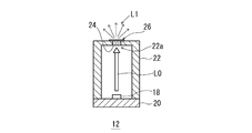
- FIG. 2 is a cross-sectional view showing a schematic configuration of a light emitting module according to the present embodiment.
- the light emitting module 12 includes a semiconductor light emitting element 18 that emits a blue laser beam, a substrate 20 on which the semiconductor light emitting element 18 is mounted, and a semiconductor light emitting element so that the laser light L0 emitted by the semiconductor light emitting element 18 does not emit in an unintended direction. It has a housing 22 for accommodating 18.
- the semiconductor light emitting device 18 preferably emits a laser beam having a peak wavelength of 380 to 480 nm, and for example, emits a blue-based (peak wavelength of about 450 nm) laser beam or a near-ultraviolet region (peak wavelength of about 405 nm). It is an element.
- the substrate 20 may also serve as a heat radiating member.
- the housing 22 is made of a material that does not transmit laser light, and an opening 22a is formed at the upper portion.
- a phosphor 24 as a wavelength conversion member that emits converted light obtained by converting the wavelength of laser light is fixed to the opening 22a.
- the phosphor 24 is, for example, a plate-shaped member made of yttrium aluminum garnet (YAG: Yttrium Aluminum Garnet) ceramics into which an activator such as cerium (Ce) has been introduced.
- the light emitting module 12 is white by mixing, for example, blue laser light emitted by the semiconductor light emitting element 18 and wavelength-converted, for example, yellow conversion light emitted by the phosphor 24 excited by the blue laser light.
- Light L1 is emitted.
- the white light L1 becomes high-intensity light having a certain degree of spread by mixing the blue laser light scattered by the phosphor 24 and the yellow wavelength-converted light having a lumbar cyan light distribution.
- the light emitting module 12 is fixed to the phosphor 24, and further includes a detection unit 26 for detecting the displacement amount of the phosphor 24.
- the detection unit 26 is configured to output an electric signal that changes according to the displacement amount of the phosphor 24.
- FIG. 3 is a cross-sectional view schematically showing the vicinity of the detection unit of the light emitting module according to the present embodiment.
- FIG. 4 is a top view schematically showing the vicinity of the detection unit of the light emitting module according to the present embodiment.
- the housing 22 has a holding portion 22b which is an insulating material surrounding the phosphor 24 fitted in the opening 22a.
- the holding portion 22b may be, for example, a ceramic material.
- the detection unit 26 is fixed to the exit surface 24a side of the phosphor 24.
- the detection unit 26 includes a wiring pattern 28 arranged on the surfaces of the holding unit 22b and the phosphor 24, an electric wire 30 connected to both ends of the wiring pattern 28, and a voltage detector 32 connected to the electric wire 30. , Have.
- the wiring pattern 28 generates a transparent conductive film 28a as an electrode formed on the emission surface 24a of the phosphor 24 and the surface 22c of the holding portion 22b, and a voltage when mechanical strain (stress) is generated.
- the piezoelectric material 28b and the piezoelectric material 28b are formed in layers.
- As the transparent conductive film 28a for example, conductive indium tin oxide (ITO: Indium Tin Oxide) is suitable. As a result, even if the wiring pattern 28 is formed on the emission surface 24a of the phosphor 24, the transmission of light is not hindered, so that the reduction in the light extraction efficiency of the light emitting module 12 as a whole is suppressed.
- ITO Indium Tin Oxide
- the piezoelectric material 28b is, for example, a thin film of zinc oxide (ZnO) having a thickness of about 3 ⁇ m.
- the piezoelectric material 28b preferably has a Curie point of 200 ° C. or higher (or 300 ° C. or higher), or a material such as ZnO that does not have a Curie point. This is because the piezoelectric material 28b may be heated by the heat generated when the phosphor 24 is excited by the laser beam L0, and if the Curie point is low, the piezoelectricity is not exhibited.
- a tensile load is applied to the YAG ceramics, it breaks at an elongation of about 4%. Therefore, in the case of the phosphor 24 of YAG ceramics having a thickness of 300 ⁇ m, it breaks when an elongation of about 12 ⁇ m occurs in the thickness direction due to a tensile load.
- the displacement amount due to thermal expansion of YAG ceramics for example, 0.36 ⁇ m
- the displacement amount caused by fracture due to the tensile load (12 ⁇ m) have a difference of 30 times or more, and the displacement amount of the phosphor is detected. Therefore, it can be estimated in advance whether or not the phosphor is likely to be destroyed.
- the piezoelectric material 28b according to the present embodiment is a ZnO thin film having a thickness of 3 ⁇ m, and has a coefficient of linear expansion of ZnO of 3.2 to 3.9 [ 10-6 / ° C.], so that the temperature change ⁇ T is 150.
- PZT lead zirconate titanate
- the coefficient of linear expansion of PZT is 2 to 4 [ 10-6 / ° C], so that the displacement when the temperature change ⁇ T is 150 ° C.
- the relationship between the displacement amount of the piezoelectric film made of PZT and the voltage is that the voltage generated by the displacement of about several ⁇ m to 10 ⁇ m is in the range of several tens V to several hundred V, and the general voltage detector 32 is used. It is sufficiently detectable. That is, when the voltage detector 32 detects a large voltage corresponding to a displacement larger than the thermal expansion of the phosphor 24 and smaller than the displacement at which breakage occurs (for example, a displacement of about 1 to 10 ⁇ m), the control unit 34 (see FIG. 3) determines that the phosphor 24 is likely to be destroyed, and stops driving the semiconductor light emitting element 18.
- the control unit 34 is, for example, an appropriate combination of an arithmetic unit, a drive circuit, and a storage circuit.
- the light emitting module 12 can estimate in advance whether or not the phosphor 24 is likely to be destroyed by detecting the displacement amount of the phosphor 24. Further, by adopting the piezoelectric material 28b as a part of the detection unit 26, the displacement amount of the phosphor 24 can be detected with a simple configuration. Further, by using a material having a Curie point of 200 ° C. or higher (or 300 ° C. or higher) or a material having no Curie point such as ZnO as the piezoelectric material 28b, even if the light emitting module 12 becomes high in temperature, the phosphor is used. It can be estimated in advance whether or not 24 is likely to be destroyed.
- the detection unit 26 can be integrally created with the phosphor 24 by laminating the transparent conductive film 28a and the piezoelectric material 28b on the phosphor 24 made of the same ceramic material.
- ZnO constituting the piezoelectric material 28b is a transparent thin film arranged so as to cover the exit surface 24a from which the light L1 converted by the phosphor 24 is emitted.
- the piezoelectric material 28b can be arranged in the region (emission surface 24a) through which the laser beam of the phosphor 24 is transmitted, and cracks and the like on the emission surface 24a of the phosphor 24 can be detected.
- the detection unit 26 similar to that of the present embodiment may be provided on the incident surface 24b side of the phosphor 24. As a result, cracks and the like on the incident surface 24b of the phosphor 24 can be detected.
- a part of the zigzag wiring pattern 28 exists on the boundary region R1 between the phosphor 24 and the holding unit 22b. Therefore, if the phosphor 24 falls off from the holding portion 22b, the displacement amount of the piezoelectric material 28b contained in a part of the wiring pattern 28 suddenly changes, and the voltage detector 32 before the wiring pattern 28 is cut. Detected as a large voltage change.
- FIG. 5 is a top view schematically showing the vicinity of the detection unit of the light emitting module according to the modified example of the present embodiment.
- the light emitting module 36 shown in FIG. 5 includes a detection unit 40 having a wiring pattern 38 formed only on the emission surface 24a of the phosphor 24.
- a detection unit 40 having a wiring pattern 38 formed only on the emission surface 24a of the phosphor 24.
- the detection unit 40 most of the wiring pattern 38 exists on the boundary region R2 between the exit surface 24a of the phosphor 24 and the holding unit 22b. Further, since the wiring pattern 38 can be shortened, the material cost for forming the detection unit can be reduced.
- FIG. 6 is a top view schematically showing the vicinity of the detection unit of the light emitting module according to another modification of the present embodiment.
- the light emitting module 42 shown in FIG. 6 does not have a wiring pattern 44 formed on the emission surface 24a of the phosphor 24. That is, most of the wiring pattern 44 is formed only on the surface 22c of the housing 22. Therefore, the light emitted from the exit surface 24a of the phosphor 24 is not obstructed.
- the holding portion 22b when the holding portion 22b is made of a ceramic material such as alumina (linear expansion coefficient 7.2 [ 10-6 / ° C]), it may be broken by thermal expansion like YAG ceramics. Even if the holding portion 22b is broken (cracked) and the phosphor 24 is dropped or broken, the voltage detector 32 detects it as a large voltage change before the wiring pattern 44 is cut. That is, by detecting the state of the holding portion 22b, it is possible to indirectly detect the falling off or breaking of the phosphor 24.
- a ceramic material such as alumina (linear expansion coefficient 7.2 [ 10-6 / ° C]
- the present invention has been described above with reference to the above-described embodiment, the present invention is not limited to the above-described embodiment, and the present invention is not limited to the above-described embodiment, and the configuration of the embodiment may be appropriately combined or replaced. It is included in the present invention. Further, it is also possible to appropriately rearrange the combination and the order of processing in the embodiment based on the knowledge of those skilled in the art, and to add modifications such as various design changes to the embodiment, and such modifications are added. Such embodiments may also be included in the scope of the present invention.
- the present invention can be used for a light emitting module using a light emitting element that emits light having a high energy density as a light source.
- Vehicle headlight unit 12 light emitting module, 18 semiconductor light emitting element, 22 housing, 22a opening, 22b holding part, 24 phosphor, 24a emitting surface, 24b incident surface, 26 detecting part, 28 wiring pattern, 28a Transparent conductive film, 28b piezoelectric material, 32 voltage detector, 34 control unit.
Landscapes
- Engineering & Computer Science (AREA)
- General Engineering & Computer Science (AREA)
- Physics & Mathematics (AREA)
- Spectroscopy & Molecular Physics (AREA)
- Optics & Photonics (AREA)
- Condensed Matter Physics & Semiconductors (AREA)
- General Physics & Mathematics (AREA)
- Electromagnetism (AREA)
- Crystallography & Structural Chemistry (AREA)
- Chemical & Material Sciences (AREA)
- Non-Portable Lighting Devices Or Systems Thereof (AREA)
- Semiconductor Lasers (AREA)
- Lighting Device Outwards From Vehicle And Optical Signal (AREA)
- Arrangement Of Elements, Cooling, Sealing, Or The Like Of Lighting Devices (AREA)
Abstract
発光モジュール(12)は、レーザ光(L0)を発する発光素子(18)と、レーザ光(L0)を波長変換した変換光(L1)を発する波長変換部材(24)と、波長変換部材(24)に固定されており、該波長変換部材(24)の変位量を検知する検知部(26)と、を備える。検知部(26)は、波長変換部材(24)の変位量に応じて変化する電気信号を出力する圧電材料(28b)を含む。
Description
本発明は、光源に高いエネルギー密度の光を発する発光素子を用いた発光モジュールに関する。
近年、より遠方を明るく照らすことが求められる様々な灯具において、レーザを光源に利用したものが考案されている。レーザが発する光はコヒーレントな光であり、非常に高いエネルギー密度を有しているため、レーザから出射されたエネルギー密度の高いレーザ光が灯具外に漏出しないような配慮が必要である。また、青色のレーザ光を発する光源と、青色のレーザ光を他の色(例えば黄色)の光に変換する蛍光体と組み合わせることで白色光を生成する発光モジュールも考案されている。
このような発光モジュールは、レーザ光が蛍光体を通過する際に散乱されるため、正常な状態ではレーザ出射時の高いエネルギー密度を有するレーザ光が灯具外に漏出することはない。しかしながら、蛍光体が割れたり所定の位置から脱落したりした場合、レーザ光が散乱されずに灯具外に漏出する可能性がある。そこで、蛍光体に電極を取り付け、蛍光体に亀裂や欠けが入った際の電極間の電気抵抗の変化から、蛍光体の亀裂等な異常を検知し、レーザをオフにする技術が考案されている(特許文献1参照)。
しかしながら、前述の技術では、実際に蛍光体に亀裂等が入らないと異常が検知できないため、蛍光体に亀裂等が入ってからレーザをオフするまでの間に漏出するレーザ光をゼロにできない。
本発明はこうした状況に鑑みてなされたものであり、その例示的な目的の一つは、高いエネルギー密度を有するレーザ光が散乱されずに外部へ漏出する可能性を低減する新たな技術を提供することにある。
上記課題を解決するために、本発明のある態様の発光モジュールは、レーザ光を発する発光素子と、レーザ光を波長変換した変換光を発する波長変換部材と、波長変換部材に固定されており、該波長変換部材の変位量を検知する検知部と、を備える。検知部は、波長変換部材の変位量に応じて変化する電気信号を出力する圧電材料を含む。
この態様によると、波長変換部材の変位量を圧電材料を用いて検知することで、波長変換部材が破壊しそうか否かを予め推測できる。また、簡易な構成で波長変換部材の変位量を検知できる。
圧電材料は、変換光が出射する波長変換部材の出射面およびレーザ光が入射する波長変換部材の入射面の少なくとも一方を覆うように配置された透明な薄膜であってもよい。これにより、波長変換部材のレーザ光が透過する領域に圧電材料を配置でき、波長変換部材の入射面や出射面における亀裂等を検知できる。
圧電材料は、キュリー点が300℃以上、または、キュリー点が存在しない材料であってもよい。これにより、仮に発光モジュールが高温になっても、波長変換部材が破壊しそうか否かを予め推測できる。
波長変換部材は、セラミックス蛍光体であってもよい。これにより、波長変換部材と検知部(例えば圧電材料)を一体に作成できる。
なお、以上の構成要素の任意の組合せ、本発明の表現を方法、装置、システム、などの間で変換したものもまた、本発明の態様として有効である。
本発明によれば、高いエネルギー密度を有するレーザ光が散乱されずに外部へ漏出する可能性を低減できる。
以下、本発明を実施の形態をもとに図面を参照しながら説明する。各図面に示される同一または同等の構成要素、部材、処理には、同一の符号を付するものとし、適宜重複した説明は省略する。また、実施の形態は、発明を限定するものではなく例示であって、実施の形態に記述される全ての特徴やその組合せは、必ずしも発明の本質的なものであるとは限らない。
(車両用灯具)
はじめに、本実施の形態に係る発光モジュールを用いた車両用灯具について説明する。車両用灯具は、例えば、高エネルギー密度の光を発する光源を用いて車両前方を遠方まで明るく照射可能な車両用前照灯ユニットである。図1は、本実施の形態に係る車両用前照灯ユニットの概略構成を示す模式図である。
はじめに、本実施の形態に係る発光モジュールを用いた車両用灯具について説明する。車両用灯具は、例えば、高エネルギー密度の光を発する光源を用いて車両前方を遠方まで明るく照射可能な車両用前照灯ユニットである。図1は、本実施の形態に係る車両用前照灯ユニットの概略構成を示す模式図である。
車両用前照灯ユニット10は、発光モジュール12と、発光モジュール12が発する光L1を車両前方へ反射する反射面14aを有するリフレクタ14と、を備える。
リフレクタ14の反射面14aは、放物面形状を有しており、下方から入射した光L1を車両前方へ平行光として反射するパラボラ光学系を構成する。発光モジュール12は、光が出射する場所が焦点F近傍となるように配置されている。なお、車両用前照灯ユニット10は、リフレクタの反射面が複合楕円面(polyellipsoid)形状である光学系を有していてもよい。
(発光モジュール)
図2は、本実施の形態に係る発光モジュールの概略構成を示す断面図である。発光モジュール12は、青色のレーザ光を発する半導体発光素子18と、半導体発光素子18が搭載される基板20と、半導体発光素子18が発するレーザ光L0が意図しない方向へ出射しないように半導体発光素子18を収容する筐体22と、を有する。
図2は、本実施の形態に係る発光モジュールの概略構成を示す断面図である。発光モジュール12は、青色のレーザ光を発する半導体発光素子18と、半導体発光素子18が搭載される基板20と、半導体発光素子18が発するレーザ光L0が意図しない方向へ出射しないように半導体発光素子18を収容する筐体22と、を有する。
半導体発光素子18は、ピーク波長が380~480nmのレーザ光を発するものがよく、例えば、青系(ピーク波長450nm程度)のレーザ光、あるいは近紫外域(ピーク波長405nm程度)のレーザ光を発する素子である。基板20は、放熱部材を兼ねていてもよい。
筐体22は、レーザ光が透過しない材質で構成されており、上部に開口部22aが形成されている。開口部22aには、レーザ光を波長変換した変換光を発する波長変換部材としての蛍光体24が固定されている。蛍光体24は、例えば、セリウム(Ce)等の付活剤が導入されたイットリウム・アルミニウム・ガーネット(YAG:Yttrium Aluminum Garnet)セラミックスからなる板状の部材である。
発光モジュール12は、半導体発光素子18が発する例えば青色のレーザ光と、青色のレーザ光によって励起された蛍光体24が発する波長変換された例えば黄色の変換光と、が混色することで、白色の光L1を出射する。白色の光L1は、蛍光体24で散乱された青色のレーザ光と、ランバーシアンな配光の黄色の波長変換光と、が混色することで、ある程度広がりのある高輝度な光となる。
本実施の形態に係る発光モジュール12は、蛍光体24に固定されており、蛍光体24の変位量を検知する検知部26を更に備える。検知部26は、蛍光体24の変位量に応じて変化する電気信号を出力するように構成されている。
図3は、本実施の形態に係る発光モジュールの検知部近傍を模式的に示した断面図である。図4は、本実施の形態に係る発光モジュールの検知部近傍を模式的に示した上面図である。
筐体22は、図3に示すように、開口部22aに嵌め込まれた蛍光体24を囲む絶縁材料である保持部22bを有する。保持部22bは、例えば、セラミック材料であってもよい。これにより、蛍光体24は、筐体22に保持、固定されている。蛍光体24の出射面24a側には、検知部26が固定されている。検知部26は、保持部22bおよび蛍光体24の表面に配置されている配線パターン28と、配線パターン28の両端に接続されている電線30と、電線30と接続されている電圧検出器32と、を有する。
配線パターン28は、蛍光体24の出射面24aおよび保持部22bの表面22cの上に形成されている電極としての透明導電膜28aと、機械的ひずみ(応力)が生じた場合に電圧を発生する圧電材料28bと、が層状に形成されている。透明導電膜28aは、例えば、導電酸化インジウムスズ(ITO:Indium Tin Oxide)が好適である。これにより、蛍光体24の出射面24aの上に配線パターン28が形成されていても、光の透過が妨げられないので、発光モジュール12全体としての光の取り出し効率の低下が抑制される。
圧電材料28bは、例えば、厚さ3μm程度の酸化亜鉛(ZnO)の薄膜である。なお、圧電材料28bは、キュリー点が200℃以上(または300℃以上)、あるいは、ZnOのようにキュリー点が存在しない材料が好ましい。蛍光体24がレーザ光L0により励起される際に発する熱によって圧電材料28bが加熱される可能性があり、キュリー点が低いと圧電性を示さなくなるからである。
蛍光体24がYAGセラミックスである場合、線膨張係数は8[10-6/℃]である。したがって、厚みが300μm程度の蛍光体24の場合、温度変化ΔTが150℃の時の変位量は、8[10-6/℃]×150℃×300μm=0.36μmとなる。一方、YAGセラミックスに対して引っ張り荷重が加わった場合、4%程度の伸びで破断する。したがって、300μmの厚みのYAGセラミックスの蛍光体24の場合、引っ張り荷重によって厚み方向に12μm程度の伸びが生じると破断する。
このように、YAGセラミックスの熱膨張による変位量(例えば0.36μm)と、引っ張り荷重によって破断が生じる変位量(12μm)とは、30倍以上の開きがあり、蛍光体の変位量を検知することで蛍光体が破壊しそうか否かを予め推測できる。
本実施の形態に係る圧電材料28bは、厚さ3μmのZnO薄膜であり、ZnOの線膨張係数が3.2~3.9[10-6/℃]であることから、温度変化ΔTが150℃の時の変位量は、3.2~3.9[10-6/℃]×150℃×3μm=0.00144~0.00176μmとなる。同様に、厚さ3μmのチタン酸ジルコン酸鉛(PZT)薄膜の場合、PZTの線膨張係数が2~4[10-6/℃]であることから、温度変化ΔTが150℃の時の変位量は、3.2~3.9[10-6/℃]×150℃×3μm=0.0009~0.0018μmとなる。
ここで、PZTからなる圧電膜の変位量と電圧との関係は、数μm~10μm程度の変位によって発生する電圧が数十Vから数百Vの範囲であり、一般的な電圧検出器32で十分検知可能である。つまり、電圧検出器32が、蛍光体24の熱膨張よりも大きな変位であって、破断が生じる変位より小さい変位(例えば1~10μm程度の変位)に対応する大きな電圧を検出した場合、制御部34(図3参照)は蛍光体24が破壊しそうな状況だと判断し、半導体発光素子18の駆動を停止する。制御部34は、例えば、演算装置や駆動回路、記憶回路を適宜組み合わせたものである。
このように、本実施の形態に係る発光モジュール12は、蛍光体24の変位量を検知することで、蛍光体24が破壊しそうか否かを予め推測できる。また、検知部26の一部に圧電材料28bを採用することで、簡易な構成で蛍光体24の変位量を検知できる。また、圧電材料28bとして、キュリー点が200℃以上(または300℃以上)、あるいは、ZnOのようにキュリー点が存在しない材料を用いることで、仮に発光モジュール12が高温になっても、蛍光体24が破壊しそうか否かを予め推測できる。
また、透明導電膜28aや圧電材料28bを、同質のセラミックス材料からなる蛍光体24の上に積層することで、検知部26を蛍光体24と一体に作成できる。
また、圧電材料28bを構成するZnOは、蛍光体24で変換された光L1が出射する出射面24aを覆うように配置された透明な薄膜である。これにより、蛍光体24のレーザ光が透過する領域(出射面24a)に圧電材料28bを配置でき、蛍光体24の出射面24aにおける亀裂等を検知できる。なお、本実施の形態と同様の検知部26を、蛍光体24の入射面24b側に設けてもよい。これにより、蛍光体24の入射面24bにおける亀裂等を検知できる。
更に本実施の形態に係る検知部26は、図4に示すように、ジグザグの配線パターン28の一部が、蛍光体24と保持部22bとの境界領域R1の上に存在する。そのため、仮に蛍光体24が保持部22bから脱落した場合、配線パターン28の一部に含まれている圧電材料28bの変位量が急変し、配線パターン28が切断する前に、電圧検出器32により大きな電圧変化として検出される。
(変形例)
図5は、本実施の形態の変形例に係る発光モジュールの検知部近傍を模式的に示した上面図である。
図5は、本実施の形態の変形例に係る発光モジュールの検知部近傍を模式的に示した上面図である。
図5に示す発光モジュール36は、図4に示す検知部26と異なり、蛍光体24の出射面24aの上にのみ形成された配線パターン38を有する検知部40を備えている。これにより、蛍光体24が変位する場合は、配線パターン38の多くも変位するため、電圧検出器32によって精度良く蛍光体24の変位量を検知できる。また、検知部40は、配線パターン38の大半が、蛍光体24の出射面24aと保持部22bとの境界領域R2の上に存在する。また、配線パターン38を短くできるので、検知部を形成する材料コストが低減できる。
また、検知部40は、図5に示すように、ジグザグの配線パターン38のほとんどが、蛍光体24と保持部22bとの境界領域R2の上に存在する。そのため、仮に蛍光体24が保持部22bから脱落した場合、配線パターン38のほとんどに含まれている圧電材料28bの変位量が急変し、配線パターン28が切断する前に、電圧検出器32により大きな電圧変化として検出される。
図6は、本実施の形態の他の変形例に係る発光モジュールの検知部近傍を模式的に示した上面図である。
図6に示す発光モジュール42は、前述の検知部26や検知部40と異なり、蛍光体24の出射面24aの上に配線パターン44が形成されていない。つまり、配線パターン44のほとんどが筐体22の表面22cにのみ形成されている。したがって、蛍光体24の出射面24aから出射する光を妨げることがない。
また、保持部22bがアルミナ(線膨張係数7.2[10-6/℃])のようなセラミック材料である場合、YAGセラミックスと同様に、熱膨張によって破断する可能性がある。仮に保持部22bに破断(クラック)が生じ、蛍光体24が脱落や破断するような場合であっても、配線パターン44が切断する前に、電圧検出器32により大きな電圧変化として検出される。つまり、保持部22bの状態を検出することで、間接的に蛍光体24の脱落や破断を検知できる。
以上、本発明を上述の実施の形態を参照して説明したが、本発明は上述の実施の形態に限定されるものではなく、実施の形態の構成を適宜組み合わせたものや置換したものについても本発明に含まれるものである。また、当業者の知識に基づいて実施の形態における組合せや処理の順番を適宜組み替えることや各種の設計変更等の変形を実施の形態に対して加えることも可能であり、そのような変形が加えられた実施の形態も本発明の範囲に含まれうる。
本発明は、光源に高いエネルギー密度の光を発する発光素子を用いた発光モジュールに利用可能である。
10 車両用前照灯ユニット、 12 発光モジュール、 18 半導体発光素子、 22 筐体、 22a 開口部、 22b 保持部、 24 蛍光体、 24a 出射面、 24b 入射面、 26 検知部、 28 配線パターン、 28a 透明導電膜、 28b 圧電材料、 32 電圧検出器、 34 制御部。
Claims (4)
- レーザ光を発する発光素子と、
前記レーザ光を波長変換した変換光を発する波長変換部材と、
前記波長変換部材に固定されており、該波長変換部材の変位量を検知する検知部と、を備え、
前記検知部は、前記波長変換部材の変位量に応じて変化する電気信号を出力する圧電材料を含むことを特徴とする発光モジュール。 - 前記圧電材料は、前記変換光が出射する前記波長変換部材の出射面および前記レーザ光が入射する前記波長変換部材の入射面の少なくとも一方を覆うように配置された透明な薄膜であることを特徴とする請求項1に記載の発光モジュール。
- 前記圧電材料は、キュリー点が300℃以上、または、キュリー点が存在しない材料であることを特徴とする請求項1または2に記載の発光モジュール。
- 前記波長変換部材は、セラミックス蛍光体であることを特徴とする請求項1乃至3のいずれか1項に記載の発光モジュール。
Priority Applications (1)
| Application Number | Priority Date | Filing Date | Title |
|---|---|---|---|
| JP2021526025A JPWO2020250757A1 (ja) | 2019-06-14 | 2020-06-02 |
Applications Claiming Priority (2)
| Application Number | Priority Date | Filing Date | Title |
|---|---|---|---|
| JP2019-111345 | 2019-06-14 | ||
| JP2019111345 | 2019-06-14 |
Publications (1)
| Publication Number | Publication Date |
|---|---|
| WO2020250757A1 true WO2020250757A1 (ja) | 2020-12-17 |
Family
ID=73736027
Family Applications (1)
| Application Number | Title | Priority Date | Filing Date |
|---|---|---|---|
| PCT/JP2020/021835 Ceased WO2020250757A1 (ja) | 2019-06-14 | 2020-06-02 | 発光モジュール |
Country Status (3)
| Country | Link |
|---|---|
| JP (1) | JPWO2020250757A1 (ja) |
| CN (2) | CN212481157U (ja) |
| WO (1) | WO2020250757A1 (ja) |
Cited By (1)
| Publication number | Priority date | Publication date | Assignee | Title |
|---|---|---|---|---|
| JP2020080400A (ja) * | 2018-11-13 | 2020-05-28 | 株式会社ダイセル | 光学部材、該光学部材を含むレーザーモジュール及びレーザーデバイス |
Families Citing this family (1)
| Publication number | Priority date | Publication date | Assignee | Title |
|---|---|---|---|---|
| WO2020250757A1 (ja) * | 2019-06-14 | 2020-12-17 | 株式会社小糸製作所 | 発光モジュール |
Citations (5)
| Publication number | Priority date | Publication date | Assignee | Title |
|---|---|---|---|---|
| JP2013168587A (ja) * | 2012-02-16 | 2013-08-29 | Sharp Corp | 発光装置、半導体レーザ素子、および照明装置 |
| JP2015060159A (ja) * | 2013-09-20 | 2015-03-30 | カシオ計算機株式会社 | 蛍光発光装置及びプロジェクタ |
| JP2016092288A (ja) * | 2014-11-07 | 2016-05-23 | スタンレー電気株式会社 | 光源装置及びこれを用いた照明装置 |
| US20160290856A1 (en) * | 2015-04-01 | 2016-10-06 | Osram Gmbh | Device and method for light conversion device monitoring |
| JP2018002912A (ja) * | 2016-07-04 | 2018-01-11 | 株式会社小糸製作所 | 焼結体および発光装置 |
Family Cites Families (6)
| Publication number | Priority date | Publication date | Assignee | Title |
|---|---|---|---|---|
| JP4975797B2 (ja) * | 2009-10-14 | 2012-07-11 | シャープ株式会社 | 照明装置、車両用灯具および車両 |
| GB2493135A (en) * | 2011-07-14 | 2013-01-30 | Barco Nv | Orbiting wavelength conversion element |
| JP6504886B2 (ja) * | 2015-04-03 | 2019-04-24 | 株式会社小糸製作所 | 車両用灯具 |
| KR20170018493A (ko) * | 2015-07-28 | 2017-02-20 | 에스엘 주식회사 | 차량용 램프 |
| CN107062128A (zh) * | 2017-06-09 | 2017-08-18 | 超视界激光科技(苏州)有限公司 | 一种自适应照明灯 |
| WO2020250757A1 (ja) * | 2019-06-14 | 2020-12-17 | 株式会社小糸製作所 | 発光モジュール |
-
2020
- 2020-06-02 WO PCT/JP2020/021835 patent/WO2020250757A1/ja not_active Ceased
- 2020-06-02 JP JP2021526025A patent/JPWO2020250757A1/ja active Pending
- 2020-06-04 CN CN202021004687.3U patent/CN212481157U/zh active Active
- 2020-06-04 CN CN202010500192.8A patent/CN112082132B/zh active Active
Patent Citations (5)
| Publication number | Priority date | Publication date | Assignee | Title |
|---|---|---|---|---|
| JP2013168587A (ja) * | 2012-02-16 | 2013-08-29 | Sharp Corp | 発光装置、半導体レーザ素子、および照明装置 |
| JP2015060159A (ja) * | 2013-09-20 | 2015-03-30 | カシオ計算機株式会社 | 蛍光発光装置及びプロジェクタ |
| JP2016092288A (ja) * | 2014-11-07 | 2016-05-23 | スタンレー電気株式会社 | 光源装置及びこれを用いた照明装置 |
| US20160290856A1 (en) * | 2015-04-01 | 2016-10-06 | Osram Gmbh | Device and method for light conversion device monitoring |
| JP2018002912A (ja) * | 2016-07-04 | 2018-01-11 | 株式会社小糸製作所 | 焼結体および発光装置 |
Cited By (1)
| Publication number | Priority date | Publication date | Assignee | Title |
|---|---|---|---|---|
| JP2020080400A (ja) * | 2018-11-13 | 2020-05-28 | 株式会社ダイセル | 光学部材、該光学部材を含むレーザーモジュール及びレーザーデバイス |
Also Published As
| Publication number | Publication date |
|---|---|
| JPWO2020250757A1 (ja) | 2020-12-17 |
| CN112082132B (zh) | 2023-05-16 |
| CN212481157U (zh) | 2021-02-05 |
| CN112082132A (zh) | 2020-12-15 |
Similar Documents
| Publication | Publication Date | Title |
|---|---|---|
| JP5841126B2 (ja) | 発光装置、照明装置、前照灯および車両 | |
| TW578315B (en) | Luminescence-diode | |
| CN101627326B (zh) | 带有半导体芯片和导光层的装置 | |
| JP6702349B2 (ja) | 発光装置 | |
| EP2458266B1 (en) | Light emitting diode (LED) lamp | |
| JP5220753B2 (ja) | 発光ダイオード照明装置 | |
| CN103486542A (zh) | 光源装置及照明装置 | |
| CN102714204B (zh) | 照明装置 | |
| TWI603033B (zh) | 包含熱導體之發光模組、燈及燈具 | |
| JP2011014535A (ja) | 照明装置 | |
| JP2016122715A (ja) | 半導体発光装置及びその駆動方法 | |
| JP5285688B2 (ja) | 発光装置、照明装置および車両用前照灯 | |
| JP6112782B2 (ja) | 照明装置 | |
| CN101128942B (zh) | Led阵列 | |
| WO2020250757A1 (ja) | 発光モジュール | |
| JP5491691B2 (ja) | 発光装置および照明器具 | |
| JP2010267851A (ja) | 発光モジュール、発光モジュールの製造方法、および灯具ユニット | |
| WO2010103840A1 (ja) | 発光モジュール、および灯具ユニット | |
| US10508791B2 (en) | Conversion of primary light into secondary light by means of a wavelength converter | |
| JP2016072263A (ja) | 発光モジュールおよび照明装置 | |
| JP4600668B2 (ja) | 面状照明装置 | |
| JP2024150736A (ja) | 発光装置、又は、光学部材 | |
| JP2014011461A (ja) | 発光ダイオードライトバー | |
| JP2017017176A (ja) | Ledモジュールおよび照明装置 | |
| JP2010504638A (ja) | 張力緩和を備える発光装置 |
Legal Events
| Date | Code | Title | Description |
|---|---|---|---|
| 121 | Ep: the epo has been informed by wipo that ep was designated in this application |
Ref document number: 20822669 Country of ref document: EP Kind code of ref document: A1 |
|
| ENP | Entry into the national phase |
Ref document number: 2021526025 Country of ref document: JP Kind code of ref document: A |
|
| NENP | Non-entry into the national phase |
Ref country code: DE |
|
| 122 | Ep: pct application non-entry in european phase |
Ref document number: 20822669 Country of ref document: EP Kind code of ref document: A1 |