WO2020245693A1 - 半導体装置 - Google Patents
半導体装置 Download PDFInfo
- Publication number
- WO2020245693A1 WO2020245693A1 PCT/IB2020/054867 IB2020054867W WO2020245693A1 WO 2020245693 A1 WO2020245693 A1 WO 2020245693A1 IB 2020054867 W IB2020054867 W IB 2020054867W WO 2020245693 A1 WO2020245693 A1 WO 2020245693A1
- Authority
- WO
- WIPO (PCT)
- Prior art keywords
- transistor
- insulator
- conductor
- oxide
- electrically connected
- Prior art date
- Legal status (The legal status is an assumption and is not a legal conclusion. Google has not performed a legal analysis and makes no representation as to the accuracy of the status listed.)
- Ceased
Links
Images















Classifications
-
- H—ELECTRICITY
- H03—ELECTRONIC CIRCUITRY
- H03F—AMPLIFIERS
- H03F3/00—Amplifiers with only discharge tubes or only semiconductor devices as amplifying elements
- H03F3/189—High-frequency amplifiers, e.g. radio frequency amplifiers
- H03F3/19—High-frequency amplifiers, e.g. radio frequency amplifiers with semiconductor devices only
- H03F3/195—High-frequency amplifiers, e.g. radio frequency amplifiers with semiconductor devices only in integrated circuits
-
- H—ELECTRICITY
- H03—ELECTRONIC CIRCUITRY
- H03F—AMPLIFIERS
- H03F3/00—Amplifiers with only discharge tubes or only semiconductor devices as amplifying elements
- H03F3/45—Differential amplifiers
- H03F3/45071—Differential amplifiers with semiconductor devices only
- H03F3/45076—Differential amplifiers with semiconductor devices only characterised by the way of implementation of the active amplifying circuit in the differential amplifier
- H03F3/45475—Differential amplifiers with semiconductor devices only characterised by the way of implementation of the active amplifying circuit in the differential amplifier using IC blocks as the active amplifying circuit
-
- H—ELECTRICITY
- H10—SEMICONDUCTOR DEVICES; ELECTRIC SOLID-STATE DEVICES NOT OTHERWISE PROVIDED FOR
- H10B—ELECTRONIC MEMORY DEVICES
- H10B12/00—Dynamic random access memory [DRAM] devices
-
- H—ELECTRICITY
- H10—SEMICONDUCTOR DEVICES; ELECTRIC SOLID-STATE DEVICES NOT OTHERWISE PROVIDED FOR
- H10D—INORGANIC ELECTRIC SEMICONDUCTOR DEVICES
- H10D30/00—Field-effect transistors [FET]
- H10D30/60—Insulated-gate field-effect transistors [IGFET]
- H10D30/67—Thin-film transistors [TFT]
-
- H—ELECTRICITY
- H10—SEMICONDUCTOR DEVICES; ELECTRIC SOLID-STATE DEVICES NOT OTHERWISE PROVIDED FOR
- H10D—INORGANIC ELECTRIC SEMICONDUCTOR DEVICES
- H10D30/00—Field-effect transistors [FET]
- H10D30/60—Insulated-gate field-effect transistors [IGFET]
- H10D30/67—Thin-film transistors [TFT]
- H10D30/6729—Thin-film transistors [TFT] characterised by the electrodes
- H10D30/673—Thin-film transistors [TFT] characterised by the electrodes characterised by the shapes, relative sizes or dispositions of the gate electrodes
- H10D30/6733—Multi-gate TFTs
- H10D30/6734—Multi-gate TFTs having gate electrodes arranged on both top and bottom sides of the channel, e.g. dual-gate TFTs
-
- H—ELECTRICITY
- H10—SEMICONDUCTOR DEVICES; ELECTRIC SOLID-STATE DEVICES NOT OTHERWISE PROVIDED FOR
- H10D—INORGANIC ELECTRIC SEMICONDUCTOR DEVICES
- H10D30/00—Field-effect transistors [FET]
- H10D30/60—Insulated-gate field-effect transistors [IGFET]
- H10D30/67—Thin-film transistors [TFT]
- H10D30/674—Thin-film transistors [TFT] characterised by the active materials
- H10D30/6755—Oxide semiconductors, e.g. zinc oxide, copper aluminium oxide or cadmium stannate
-
- H—ELECTRICITY
- H10—SEMICONDUCTOR DEVICES; ELECTRIC SOLID-STATE DEVICES NOT OTHERWISE PROVIDED FOR
- H10D—INORGANIC ELECTRIC SEMICONDUCTOR DEVICES
- H10D30/00—Field-effect transistors [FET]
- H10D30/60—Insulated-gate field-effect transistors [IGFET]
- H10D30/67—Thin-film transistors [TFT]
- H10D30/6757—Thin-film transistors [TFT] characterised by the structure of the channel, e.g. transverse or longitudinal shape or doping profile
-
- H—ELECTRICITY
- H10—SEMICONDUCTOR DEVICES; ELECTRIC SOLID-STATE DEVICES NOT OTHERWISE PROVIDED FOR
- H10D—INORGANIC ELECTRIC SEMICONDUCTOR DEVICES
- H10D62/00—Semiconductor bodies, or regions thereof, of devices having potential barriers
- H10D62/80—Semiconductor bodies, or regions thereof, of devices having potential barriers characterised by the materials
- H10D62/81—Semiconductor bodies, or regions thereof, of devices having potential barriers characterised by the materials of structures exhibiting quantum-confinement effects, e.g. single quantum wells; of structures having periodic or quasi-periodic potential variation
-
- H—ELECTRICITY
- H10—SEMICONDUCTOR DEVICES; ELECTRIC SOLID-STATE DEVICES NOT OTHERWISE PROVIDED FOR
- H10D—INORGANIC ELECTRIC SEMICONDUCTOR DEVICES
- H10D84/00—Integrated devices formed in or on semiconductor substrates that comprise only semiconducting layers, e.g. on Si wafers or on GaAs-on-Si wafers
- H10D84/01—Manufacture or treatment
- H10D84/0123—Integrating together multiple components covered by H10D12/00 or H10D30/00, e.g. integrating multiple IGBTs
- H10D84/0126—Integrating together multiple components covered by H10D12/00 or H10D30/00, e.g. integrating multiple IGBTs the components including insulated gates, e.g. IGFETs
- H10D84/0128—Manufacturing their channels
-
- H—ELECTRICITY
- H10—SEMICONDUCTOR DEVICES; ELECTRIC SOLID-STATE DEVICES NOT OTHERWISE PROVIDED FOR
- H10D—INORGANIC ELECTRIC SEMICONDUCTOR DEVICES
- H10D84/00—Integrated devices formed in or on semiconductor substrates that comprise only semiconducting layers, e.g. on Si wafers or on GaAs-on-Si wafers
- H10D84/01—Manufacture or treatment
- H10D84/02—Manufacture or treatment characterised by using material-based technologies
- H10D84/03—Manufacture or treatment characterised by using material-based technologies using Group IV technology, e.g. silicon technology or silicon-carbide [SiC] technology
- H10D84/038—Manufacture or treatment characterised by using material-based technologies using Group IV technology, e.g. silicon technology or silicon-carbide [SiC] technology using silicon technology, e.g. SiGe
-
- H—ELECTRICITY
- H10—SEMICONDUCTOR DEVICES; ELECTRIC SOLID-STATE DEVICES NOT OTHERWISE PROVIDED FOR
- H10D—INORGANIC ELECTRIC SEMICONDUCTOR DEVICES
- H10D84/00—Integrated devices formed in or on semiconductor substrates that comprise only semiconducting layers, e.g. on Si wafers or on GaAs-on-Si wafers
- H10D84/01—Manufacture or treatment
- H10D84/02—Manufacture or treatment characterised by using material-based technologies
- H10D84/08—Manufacture or treatment characterised by using material-based technologies using combinations of technologies, e.g. using both Si and SiC technologies or using both Si and Group III-V technologies
-
- H—ELECTRICITY
- H10—SEMICONDUCTOR DEVICES; ELECTRIC SOLID-STATE DEVICES NOT OTHERWISE PROVIDED FOR
- H10D—INORGANIC ELECTRIC SEMICONDUCTOR DEVICES
- H10D84/00—Integrated devices formed in or on semiconductor substrates that comprise only semiconducting layers, e.g. on Si wafers or on GaAs-on-Si wafers
- H10D84/80—Integrated devices formed in or on semiconductor substrates that comprise only semiconducting layers, e.g. on Si wafers or on GaAs-on-Si wafers characterised by the integration of at least one component covered by groups H10D12/00 or H10D30/00, e.g. integration of IGFETs
-
- H—ELECTRICITY
- H10—SEMICONDUCTOR DEVICES; ELECTRIC SOLID-STATE DEVICES NOT OTHERWISE PROVIDED FOR
- H10D—INORGANIC ELECTRIC SEMICONDUCTOR DEVICES
- H10D84/00—Integrated devices formed in or on semiconductor substrates that comprise only semiconducting layers, e.g. on Si wafers or on GaAs-on-Si wafers
- H10D84/80—Integrated devices formed in or on semiconductor substrates that comprise only semiconducting layers, e.g. on Si wafers or on GaAs-on-Si wafers characterised by the integration of at least one component covered by groups H10D12/00 or H10D30/00, e.g. integration of IGFETs
- H10D84/811—Combinations of field-effect devices and one or more diodes, capacitors or resistors
-
- H—ELECTRICITY
- H10—SEMICONDUCTOR DEVICES; ELECTRIC SOLID-STATE DEVICES NOT OTHERWISE PROVIDED FOR
- H10D—INORGANIC ELECTRIC SEMICONDUCTOR DEVICES
- H10D84/00—Integrated devices formed in or on semiconductor substrates that comprise only semiconducting layers, e.g. on Si wafers or on GaAs-on-Si wafers
- H10D84/80—Integrated devices formed in or on semiconductor substrates that comprise only semiconducting layers, e.g. on Si wafers or on GaAs-on-Si wafers characterised by the integration of at least one component covered by groups H10D12/00 or H10D30/00, e.g. integration of IGFETs
- H10D84/82—Integrated devices formed in or on semiconductor substrates that comprise only semiconducting layers, e.g. on Si wafers or on GaAs-on-Si wafers characterised by the integration of at least one component covered by groups H10D12/00 or H10D30/00, e.g. integration of IGFETs of only field-effect components
- H10D84/83—Integrated devices formed in or on semiconductor substrates that comprise only semiconducting layers, e.g. on Si wafers or on GaAs-on-Si wafers characterised by the integration of at least one component covered by groups H10D12/00 or H10D30/00, e.g. integration of IGFETs of only field-effect components of only insulated-gate FETs [IGFET]
-
- H—ELECTRICITY
- H10—SEMICONDUCTOR DEVICES; ELECTRIC SOLID-STATE DEVICES NOT OTHERWISE PROVIDED FOR
- H10D—INORGANIC ELECTRIC SEMICONDUCTOR DEVICES
- H10D86/00—Integrated devices formed in or on insulating or conducting substrates, e.g. formed in silicon-on-insulator [SOI] substrates or on stainless steel or glass substrates
- H10D86/40—Integrated devices formed in or on insulating or conducting substrates, e.g. formed in silicon-on-insulator [SOI] substrates or on stainless steel or glass substrates characterised by multiple TFTs
- H10D86/421—Integrated devices formed in or on insulating or conducting substrates, e.g. formed in silicon-on-insulator [SOI] substrates or on stainless steel or glass substrates characterised by multiple TFTs having a particular composition, shape or crystalline structure of the active layer
- H10D86/423—Integrated devices formed in or on insulating or conducting substrates, e.g. formed in silicon-on-insulator [SOI] substrates or on stainless steel or glass substrates characterised by multiple TFTs having a particular composition, shape or crystalline structure of the active layer comprising semiconductor materials not belonging to the Group IV, e.g. InGaZnO
-
- H—ELECTRICITY
- H10—SEMICONDUCTOR DEVICES; ELECTRIC SOLID-STATE DEVICES NOT OTHERWISE PROVIDED FOR
- H10D—INORGANIC ELECTRIC SEMICONDUCTOR DEVICES
- H10D86/00—Integrated devices formed in or on insulating or conducting substrates, e.g. formed in silicon-on-insulator [SOI] substrates or on stainless steel or glass substrates
- H10D86/40—Integrated devices formed in or on insulating or conducting substrates, e.g. formed in silicon-on-insulator [SOI] substrates or on stainless steel or glass substrates characterised by multiple TFTs
- H10D86/481—Integrated devices formed in or on insulating or conducting substrates, e.g. formed in silicon-on-insulator [SOI] substrates or on stainless steel or glass substrates characterised by multiple TFTs integrated with passive devices, e.g. auxiliary capacitors
-
- H—ELECTRICITY
- H10—SEMICONDUCTOR DEVICES; ELECTRIC SOLID-STATE DEVICES NOT OTHERWISE PROVIDED FOR
- H10D—INORGANIC ELECTRIC SEMICONDUCTOR DEVICES
- H10D86/00—Integrated devices formed in or on insulating or conducting substrates, e.g. formed in silicon-on-insulator [SOI] substrates or on stainless steel or glass substrates
- H10D86/40—Integrated devices formed in or on insulating or conducting substrates, e.g. formed in silicon-on-insulator [SOI] substrates or on stainless steel or glass substrates characterised by multiple TFTs
- H10D86/60—Integrated devices formed in or on insulating or conducting substrates, e.g. formed in silicon-on-insulator [SOI] substrates or on stainless steel or glass substrates characterised by multiple TFTs wherein the TFTs are in active matrices
-
- H—ELECTRICITY
- H10—SEMICONDUCTOR DEVICES; ELECTRIC SOLID-STATE DEVICES NOT OTHERWISE PROVIDED FOR
- H10D—INORGANIC ELECTRIC SEMICONDUCTOR DEVICES
- H10D88/00—Three-dimensional [3D] integrated devices
- H10D88/01—Manufacture or treatment
-
- H—ELECTRICITY
- H03—ELECTRONIC CIRCUITRY
- H03F—AMPLIFIERS
- H03F2200/00—Indexing scheme relating to amplifiers
- H03F2200/129—Indexing scheme relating to amplifiers there being a feedback over the complete amplifier
-
- H—ELECTRICITY
- H03—ELECTRONIC CIRCUITRY
- H03F—AMPLIFIERS
- H03F2203/00—Indexing scheme relating to amplifiers with only discharge tubes or only semiconductor devices as amplifying elements covered by H03F3/00
- H03F2203/20—Indexing scheme relating to power amplifiers, e.g. Class B amplifiers, Class C amplifiers
- H03F2203/21—Indexing scheme relating to power amplifiers, e.g. Class B amplifiers, Class C amplifiers with semiconductor devices only
- H03F2203/211—Indexing scheme relating to power amplifiers, e.g. Class B amplifiers, Class C amplifiers with semiconductor devices only using a combination of several amplifiers
- H03F2203/21112—A filter circuit being added at the input of a power amplifier stage
-
- H—ELECTRICITY
- H03—ELECTRONIC CIRCUITRY
- H03F—AMPLIFIERS
- H03F2203/00—Indexing scheme relating to amplifiers with only discharge tubes or only semiconductor devices as amplifying elements covered by H03F3/00
- H03F2203/45—Indexing scheme relating to differential amplifiers
- H03F2203/45528—Indexing scheme relating to differential amplifiers the FBC comprising one or more passive resistors and being coupled between the LC and the IC
-
- H—ELECTRICITY
- H03—ELECTRONIC CIRCUITRY
- H03F—AMPLIFIERS
- H03F2203/00—Indexing scheme relating to amplifiers with only discharge tubes or only semiconductor devices as amplifying elements covered by H03F3/00
- H03F2203/45—Indexing scheme relating to differential amplifiers
- H03F2203/45594—Indexing scheme relating to differential amplifiers the IC comprising one or more resistors, which are not biasing resistor
Definitions
- One aspect of the present invention relates to a semiconductor device.
- one aspect of the present invention is not limited to the above technical fields.
- the technical field of the invention disclosed in the present specification and the like relates to a product, a method, or a manufacturing method.
- one aspect of the invention relates to a process, machine, manufacture, or composition (composition of matter).
- the semiconductor device refers to all devices that can function by utilizing the semiconductor characteristics. Therefore, semiconductor elements such as transistors and diodes, and circuits including semiconductor elements are semiconductor devices.
- semiconductor elements such as transistors and diodes, and circuits including semiconductor elements are semiconductor devices.
- display devices, light emitting devices, lighting devices, electro-optical devices, communication devices, electronic devices, and the like may include semiconductor elements and semiconductor circuits. Therefore, display devices, light emitting devices, lighting devices, electro-optic devices, image pickup devices, communication devices, electronic devices, and the like may also be referred to as semiconductor devices.
- the 5th generation mobile communication system (5G) is being introduced, but communication delay is one of the major problems in providing a communication environment. Communication delays not only impair the merits of 5G, but also lead to difficulty in providing comfortable services in an environment with an eye on Internet of Things (IoT).
- Edge computing is being considered as a measure to eliminate communication delays. Edge computing is at least via a relay station between the central base and the user terminal. The relay bases are installed near the user terminals and more than the central bases. It is expected that such edge computing can reduce the communication delay that occurs between the central base and the user terminal.
- the relay base needs to be installed near the user terminal, but considering the installation location and installation cost, it is difficult to install a relay base with new construction. Therefore, it is conceivable to install the relay station in an existing building (office building, commercial building, etc.).
- Semiconductor devices compatible with 5G are manufactured using semiconductors that use one type of element such as Si as the main component and compound semiconductors that use multiple types of elements such as Ga and As as the main components. Furthermore, oxide semiconductors, which are a type of metal oxide, are attracting attention.
- Non-Patent Document 1 In oxide semiconductors, CAAC (c-axis aligned crystalline) structures and nc (nanocrystalline) structures that are neither single crystal nor amorphous have been found (see Non-Patent Document 1 and Non-Patent Document 2).
- Non-Patent Document 1 and Non-Patent Document 2 disclose a technique for manufacturing a transistor using an oxide semiconductor having a CAAC structure.
- an object of the present invention is to provide a communication device that has achieved miniaturization while having a function as a relay base.
- Such communication equipment can be referred to as a semiconductor device or an electronic device.
- the present invention has a transistor and the operational amplifier having an operational amplifier between the input terminal of the phase shifter and the output terminal of the phase shifter and electrically connected to the first input terminal of the operational amplifier.
- the transistor has a first resistance element electrically connected to the second input terminal of the operational amplifier and a second resistance element electrically connected to the second input terminal of the operational amplifier.
- the gate is electrically connected to the first terminal, one of the source or drain of the transistor is electrically connected to the input terminal of the phase shifter, and the other of the source or drain of the transistor is of the operational amplifier. It is electrically connected to the first input terminal, the first resistance element is electrically connected to the input terminal of the phase shifter, and the second resistance element is electrically connected to the output terminal of the phase shifter.
- the transistor connected to the operational amplifier and having at least the operational amplifier has a region overlapping with the transistor. At least the transistor included in the operational amplifier has a region overlapping with the transistor, so that a miniaturized phase shifter can be provided.
- the present invention has a transistor having an operational amplifier between the input terminal of the phase shifter and the output terminal of the phase shifter and electrically connected to the first input terminal of the operational amplifier, and the first.
- the storage element electrically connected to the gate of one transistor, the first resistance element electrically connected to the second input terminal of the operational amplifier, and the second input terminal of the operational amplifier and electricity. It has a second resistance element connected to the transistor, the gate of the transistor is electrically connected to the first terminal, and one of the source or drain of the transistor is connected to the input terminal of the phase shifter. Electrically connected, the other of the source or drain of the transistor is electrically connected to the first input terminal of the operational amplifier, and the first resistance element is electrically connected to the input terminal of the phase shifter.
- the second resistance element is electrically connected to the output terminal of the phase shifter, and at least the transistor included in the operational amplifier has a region overlapping with the transistor. Since at least the transistor included in the operational amplifier has a region overlapping with the first transistor, it is possible to provide a miniaturized phase shifter.
- the storage element has a first transistor and a first capacitive element
- the first transistor has an oxide semiconductor film
- at least the transistor of the operational amplifier is the first transistor. It may have a region overlapping with one transistor.
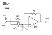
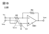
- FIG. 1A and 1B are views showing the semiconductor device of the present invention.
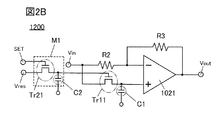
- 2A and 2B are diagrams showing the semiconductor device of the present invention.
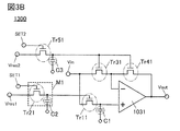
- 3A and 3B are diagrams showing the semiconductor device of the present invention.
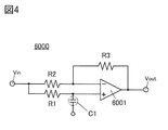
- FIG. 4 is a diagram showing a semiconductor device.
- FIG. 5 is a diagram showing a semiconductor device of the present invention.
- FIG. 6 is a diagram showing a semiconductor device of the present invention.
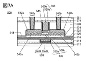
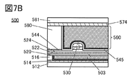
- 7A, 7B, and 7C are diagrams showing the semiconductor device of the present invention.
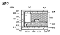
- 8A, 8B, and 8C are diagrams showing the semiconductor device of the present invention.
- 9A, 9B, and 9C are diagrams showing the semiconductor device of the present invention.
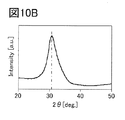
- 10A, 10B, and 10C are diagrams showing the oxide semiconductor of the present invention.
- FIGS. 11A and 11B are diagrams showing the semiconductor device of the present invention.
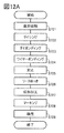
- 12A and 12B are diagrams showing the semiconductor device of the present invention.
- FIG. 13 is a diagram showing a usage pattern of the present invention.
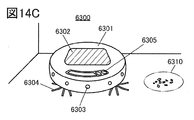
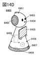
- 14A, 14B, 14C, 14D, 14E, and 14F are views showing a usage pattern of the present invention.
- FIG. 15 is a diagram showing a usage pattern of the present invention.
- FIG. 16 is a diagram showing a usage pattern of the present invention.
- the position, size, range, etc. of each configuration shown in the drawings, etc. may not represent the actual position, size, range, etc. in order to facilitate understanding of the invention. Therefore, the disclosed invention is not necessarily limited to the position, size, range, etc. disclosed in the drawings and the like.
- the resist mask or the like may be unintentionally reduced due to a process such as etching, but it may not be reflected in the drawing for easy understanding.
- electrode and “wiring” in the present specification and the like do not functionally limit these components.
- an “electrode” may be used as part of a “wiring” and vice versa.
- the terms “electrode” and “wiring” include the case where a plurality of “electrodes” and “wiring” are integrally formed.
- the "terminal" in the electric circuit means a part where current input or output, voltage input or output, or signal reception or transmission is performed. Therefore, a part of the wiring or the electrode may function as a terminal.
- the terms “upper” and “lower” in the present specification and the like do not limit the positional relationship of the components to be directly above or directly below and to be in direct contact with each other.
- electrode B on the insulating layer A it is not necessary that the electrode B is formed in direct contact with the insulating layer A, and another configuration is formed between the insulating layer A and the electrode B. Do not exclude those that contain elements.
- source and drain functions are interchanged depending on operating conditions, such as when transistors with different polarities are used or when the direction of current changes during circuit operation, so which one is the source or drain is limited. Is difficult. Therefore, in the present specification, the terms source and drain can be used interchangeably.
- electrically connected includes a case of being directly connected and a case of being connected via "something having some electrical action".
- the "thing having some kind of electrical action” is not particularly limited as long as it enables the exchange of electric signals between the connection targets. Therefore, even when it is expressed as “electrically connected", in an actual circuit, there is a case where there is no physical connection part and only the wiring is extended.
- parallel means, for example, a state in which two straight lines are arranged at an angle of -10 ° or more and 10 ° or less. Therefore, the case of ⁇ 5 ° or more and 5 ° or less is also included.
- vertical and orthogonal mean, for example, a state in which two straight lines are arranged at an angle of 80 ° or more and 100 ° or less. Therefore, the case of 85 ° or more and 95 ° or less is also included.
- the voltage often indicates the potential difference between a certain potential and a reference potential (for example, ground potential or source potential). Therefore, it is often possible to paraphrase voltage and potential. In the present specification and the like, voltage and potential can be paraphrased unless otherwise specified.
- semiconductor Even when the term "semiconductor” is used, for example, if the conductivity is sufficiently low, it has the characteristics of an "insulator". Therefore, it is possible to replace “semiconductor” with “insulator". In this case, the boundary between “semiconductor” and “insulator” is ambiguous, and it is difficult to make a strict distinction between the two. Therefore, the terms “semiconductor” and “insulator” described herein may be interchangeable.
- ordinal numbers such as “first" and “second” in the present specification and the like are added to avoid confusion of the components, and do not indicate any order or order such as process order or stacking order. ..
- terms that do not have ordinal numbers in the present specification and the like may have ordinal numbers within the scope of claims in order to avoid confusion of components.
- different ordinal numbers may be added within the scope of claims.
- the ordinal numbers may be omitted in the scope of claims.
- the "on state” of the transistor means a state in which the source and drain of the transistor can be regarded as being electrically short-circuited (also referred to as “conduction state”).
- the “off state” of the transistor means a state in which the source and drain of the transistor can be regarded as being electrically cut off (also referred to as “non-conducting state”).
- the "on current” may mean the current flowing between the source and the drain when the transistor is in the on state.
- the “off current” may mean a current flowing between the source and the drain when the transistor is in the off state.
- the high power supply potential VDD (hereinafter, also simply referred to as “VDD”, “H potential”, or “H”) refers to the low power supply potential VSS (hereinafter, simply “VSS”, “L potential”). , Or also referred to as “L”), indicating a power supply potential with a higher potential.
- VSS indicates a power supply potential having a potential lower than VDD.
- the ground potential (hereinafter, also simply referred to as “GND” or “GND potential”) can be used as VDD or VSS.
- VDD is the ground potential
- VSS is a potential lower than the ground potential
- VDD is a potential higher than the ground potential.
- the gate means a part or all of the gate electrode and the gate wiring.
- the gate wiring refers to wiring for electrically connecting the gate electrode of at least one transistor with another electrode or another wiring.
- the source means a part or all of a source area, a source electrode, and a source wiring.
- the source region refers to a region of the semiconductor layer having a resistivity of a certain value or less.
- the source electrode refers to a conductive layer in a portion connected to the source region.
- the source wiring is a wiring for electrically connecting the source electrode of at least one transistor to another electrode or another wiring.
- the drain means a part or all of the drain region, the drain electrode, and the drain wiring.
- the drain region refers to a region of the semiconductor layer having a resistivity of a certain value or less.
- the drain electrode refers to a conductive layer at a portion connected to the drain region.
- Drain wiring refers to wiring for electrically connecting the drain electrode of at least one transistor to another electrode or another wiring.
- H indicating the H potential
- L indicating the L potential
- “H” or “L” may be added with enclosing characters to the wiring and electrodes where the potential change has occurred.
- an “x” symbol may be added over the transistor.
- the 5G communication frequency band includes a frequency band up to 6 GHz and a frequency band from around 30 GHz to about 100 GHz.
- Japan there is a movement to make both of the above frequency bands available, and a specific frequency of the above frequency bands is assigned to each carrier. Therefore, it is expected that the frequency used will differ depending on the user terminal. Looking at other countries, the frequency band used varies depending on the circumstances of each country. Based on these, communication equipment must support a large number of frequencies.
- the phase shifter 6000 shown in FIG. 4 has an input terminal Vin and an output terminal Vout.
- the phase shifter 6000 includes an operational amplifier 6001, a resistance element R1 to a resistance element R3, and a capacitance element C1.
- the resistance element R1 is electrically connected between the input terminal Vin of the phase shifter 6000 and the non-inverting input terminal (+ side terminal, first input terminal) of the operational amplifier 6001. That is, the signal from the input terminal Vin is input to the operational amplifier 6001 via the resistance element R1.
- the resistance element R2 is electrically connected between the input terminal Vin of the phase shifter 6000 and the inverting input terminal (-side terminal, second input terminal) of the operational amplifier 6001. That is, the signal from the input terminal Vin is input to the operational amplifier 6001 via the resistance element R2.
- the resistance element R3 is electrically connected between the second input terminal of the operational amplifier 6001 and the output terminal Vout of the phase shifter 6000. That is, the resistance element R3 is arranged in the feedback circuit.
- the output terminal Vout of the phase shifter 6000 is equal to the output terminal of the operational amplifier 6001.
- the capacitance element C1 is electrically connected to the resistance element R1 and the first input terminal.
- phase shifter 6000 the phase of the output terminal Vout with respect to the input terminal Vin is as follows.
- ⁇ is the angular frequency.
- ⁇ is the amount of change in phase shift between the input waveform and the output waveform.
- C 1 is a capacitance value of the capacitance element C1 shown in FIG.
- R 1 is the resistance value of the resistance element R1 shown in FIG.
- R is the resistance value of the resistance element R2 shown in FIG. 4
- the resistance value of the resistance element R3 shown in FIG. 4 is equal to the resistance value of the resistance element R2.
- the phase shifter can function as a communication device, a semiconductor device, or an electronic device. That is, the phase shifter can be referred to as a communication device, a semiconductor device, or an electronic device. It can also be said that the communication device, the semiconductor device, or the electronic device arranged at the relay base has a phase shifter.
- the phase shifter 1100 shown in FIG. 1A has a transistor Tr1. That is, the phase shifter 1100 shown in FIG. 1A has an operational amplifier 1001, has a transistor Tr1 electrically connected to the first input terminal of the operational amplifier 1001, and is electrically connected to the second input terminal of the operational amplifier 1001. It has a resistance element R2 and a resistance element R3. The gate of the transistor Tr1 is electrically connected to the terminal Vres. One of the source or drain of the transistor Tr1 and the first input terminal of the operational amplifier 1001 are electrically connected to each other, and the capacitive element C1 is electrically connected to the one and the first input terminal.
- the other side of the source or drain of the transistor Tr1 is electrically connected to the input terminal Vin of the phase shifter 1100.
- the resistance element R2 is also electrically connected to the input terminal Vin.
- the resistance element R3 is electrically connected to the second output terminal of the operational amplifier 1001 and is also electrically connected to the output terminal of the operational amplifier 1001. That is, the resistance element R3 is arranged in the feedback circuit.
- the output terminal of the operational amplifier 1001 is equal to the output terminal Vout of the phase shifter 1100.
- the gate of the transistor Tr1 is electrically connected to the terminal Vres, and a signal for controlling the gate is supplied from the terminal Vres. Depending on the signal, the transistor Tr1 can be turned on or off.
- the resistance of the transistor Tr1 in the off state (off resistance) is higher than the resistance in the on state (on resistance).
- the on-resistance can take various resistance values depending on the linearity of vd-Id of the transistor Tr1. That is, the on-resistance of the transistor Tr1 can be controlled by a signal from the terminal Vres.
- the transistor Tr1 has four terminals. That is, the transistor Tr1 has a terminal for a back gate. By supplying a signal to the back gate terminal, it is possible to control the threshold value of the transistor Tr1 and the like.
- the transistor Tr1 in the phase shifter 1100 may have at least three terminals. Therefore, FIG. 1B shows a configuration example having a transistor Tr11 having three terminals corresponding to the transistor Tr1. In FIG. 1B, other configurations are the same as in FIG. 1A.
- the capacitance element C1 can be reduced. Further, the capacitive element C1 can be omitted. If the capacitive element C1 can be made smaller or omitted, the phase shifter 1100 can be further made smaller.
- the active layer of the above-mentioned transistor may be silicon or an oxide semiconductor. If silicon is used, the mobility is high, so it is expected that the phase shifter will operate at high speed. When the oxide semiconductor is adopted, the off-current can be lowered in the above-mentioned transistor, so that the capacitive element can be omitted as described above. It can contribute to reducing the area of the phase shifter. Further, instead of the capacitance element described above, the gate capacitance of the transistor described above can be adopted.
- the transistor having silicon in the active layer can have a three-terminal configuration as shown in FIG. 1B.
- phase shifter 1200 of FIGS. 2A and 2B has a configuration in which a transistor Tr2 and a capacitance element C2 are added to the phase shifter 1100 of FIGS. 1A and 1B.
- the resistance elements at the same locations as those in FIG. 4 are designated by the same reference numerals as those in FIG.
- the newly provided transistor Tr2 and the capacitive element C2 function as the storage element M1.
- the storage element M1 can hold an electric charge or the like in the capacitance element C2.
- the phase shifter 1200 shown in FIG. 2A has an operational amplifier 1021 and has a transistor Tr1 electrically connected to the first input terminal of the operational amplifier 1021 and is electrically connected to the second input terminal of the operational amplifier 1021. It also has a resistance element R2 and a resistance element R3.
- the gate of the transistor Tr1 is electrically connected to the storage element M1.
- the storage element M1 has a transistor Tr2 and a capacitance element C2.
- the gate of the transistor Tr1 is electrically connected to either the source or the drain of the transistor Tr2.
- the gate of the transistor Tr1 is electrically connected to the capacitive element C2.
- the gate of the transistor Tr2 is electrically connected to the terminal SET.
- the other of the source or drain of the transistor Tr2 is electrically connected to the terminal Vres.
- the gate of the transistor Tr1 is electrically connected to the storage element M1.
- the transistor Tr1 is controlled by the storage element M1.
- the storage element M1 can hold a potential that turns on the transistor Tr1. Since it is not necessary to supply a new signal to the terminal SET or the like during the holding, the power consumption of the phase shifter 1200 can be reduced.
- One of the source or drain of the transistor Tr1 is electrically connected to the first input terminal of the operational amplifier 1021, and the other is electrically connected to the input terminal Vin of the phase shifter 1200.
- the resistance element R2 is also electrically connected to the input terminal Vin.
- the resistance element R3 is electrically connected to the second output terminal of the operational amplifier 1021 and is also electrically connected to the output terminal of the operational amplifier 1021. That is, the resistance element R3 is arranged in the feedback circuit.
- the output terminal of the operational amplifier 1021 is equal to the output terminal Vout of the phase shifter 1100.
- FIG. 2A has a transistor Tr1 and a transistor Tr2 having four terminals.
- FIG. 2B shows a case where the transistor Tr11 and the transistor Tr21 having three terminals are provided. Other configurations are the same as in FIG. 2A.
- the capacitance element C1 can be reduced. Further, the capacitive element C1 can be omitted. If the capacitive element C1 can be made smaller or omitted, the phase shifter 1200 can be further made smaller.
- the storage element M1 shown in FIGS. 2A and 2B makes it possible to reduce the power consumption of the phase shifter 1200.
- FIGS. 2A and 2B Modification examples of the phase shifters shown in FIGS. 2A and 2B will be described with reference to FIGS. 3A and 3B, respectively.
- 3A and 3B are configuration examples in which a transistor is also used for the resistance element on the negative feedback side. That is, in the phase shifter 1300 of FIGS. 3A and 3B, the transistors Tr3 to Tr5 and the capacitance element C3 are added to each of FIGS. 2A and 2B.
- the phase shifter 1300 shown in FIG. 3A has an operational amplifier 1031, has a transistor Tr1 electrically connected to the first input terminal of the operational amplifier 1031, and is electrically connected to the second input terminal of the operational amplifier 1031. It also has a transistor Tr3 and a transistor Tr4.
- the transistor Tr1 and the storage element M1 are the same as those in FIG. 2A, but in FIG. 3A, the terminal Vres of FIG. 2A is referred to as the terminal Vres1, and the terminal SET of FIG. 2A is ordinalized as the terminal SET1. Both the gates of the transistor Tr3 and the transistor Tr4 are electrically connected to either the source or the drain of the transistor Tr5.
- One of the source and drain of the transistor Tr3 is electrically connected to the input terminal Vin of the phase shifter 1300.
- the other of the source or drain of the transistor Tr3 is electrically connected to one of the source or drain of the transistor Tr4 and is electrically connected to the second input terminal of the operational amplifier 1031.
- the other side of the source or drain of the transistor Tr4 is electrically connected to the output terminal of the phase shifter 1300.
- the gate of the transistor Tr5 is electrically connected to the terminal SET2.
- One of the source and drain of the transistor Tr5 is electrically connected to the capacitive element C3.
- the other of the source or drain of the transistor Tr5 is electrically connected to the terminal Vres2.
- FIG. 3A has transistors Tr1 to Tr5 having four terminals.
- FIG. 3B shows a case where the transistors Tr11, Tr21, Tr31, Tr41, and Tr51 having three terminals are provided. Other configurations are the same as in FIG. 3A.
- the capacitance element C1 can be reduced. Further, the capacitive element C1 can be omitted. If the capacitive element C1 can be made smaller or omitted, the phase shifter 1300 can be further made smaller.
- the capacitance element C3 can be reduced. Further, the capacitive element C3 can be omitted. If the capacitive element C3 can be made smaller or omitted, the phase shifter 1300 can be further made smaller.
- the phase shifter 1300 shown in FIGS. 3A and 3B can expand the applicable frequency band.
- FIG. 5 A part of the cross-sectional structure of the semiconductor device is shown in FIG.
- the semiconductor device shown in FIG. 5 is an example in which a transistor 550, a transistor 500, and a capacitance element 600 are laminated in order, and a semiconductor device such as a phase shifter is provided by such a laminated structure. It can be miniaturized.
- the transistor 500 has a conductor 592 that functions as a back gate terminal and a conductor 593 that functions as a gate terminal.
- the conductor 592 that functions as a back gate terminal can be omitted.
- the operational amplifier described above can have a transistor 550 having silicon in the active layer, and transistors Tr1 to Tr5 can have a transistor 500 having an oxide semiconductor in the active layer. At least the transistor 550 of the operational amplifier has a region overlapping with the transistor 500. Therefore, the phase shifter can be miniaturized. Further, the above-mentioned capacitance elements C1 to C3 can have a capacitance element 600. Further miniaturization of the phase shifter can be achieved by reducing the area of the capacitive element 600.
- the transistor 500 has an oxide semiconductor in the active layer and can be called an OS transistor.
- the transistor 500 has an extremely small off current. Therefore, the data voltage or electric charge written to the storage node via the transistor 500 can be held in the storage node for a long period of time.
- the phase shifter shown in FIGS. 2A and 2B by applying the effect of the OS transistor to the storage element M1 provided with the capacitance element C2, the data voltage or charge can be held in the capacitance element C2 for a long period of time. It will be possible. The power consumption of semiconductor devices such as phase shifters can be reduced.
- the transistor 550 is provided on the substrate 311 and has a semiconductor region 313, a low resistance region 314a, and a low resistance region 314b, which are composed of a conductor 316, an insulator 315, and a part of the substrate 311.
- the conductor 316 functions as a gate for the transistor 550.
- the insulator 315 functions as a gate insulating layer of the transistor 550.
- the semiconductor region 313 functions as a channel forming region.
- the low resistance region 314a and the low resistance region 314b function as one and the other of the source region or the drain region, respectively.
- the transistor 550 has silicon in the active layer and has higher mobility than the OS transistor, and can contribute to high-speed operation of the operational amplifier.
- FIG. 7A is a cross-sectional view of the transistor 500 in the channel length direction
- FIG. 7B is a cross-sectional view of the transistor 500 in the channel width direction.
- FIG. 7C is a cross-sectional view of the transistor 550 in the channel width direction.
- the upper part of the semiconductor region 313 of the transistor 550 is covered with the conductor 316 via the insulator 315. It is a so-called Fin type.
- Fin type By making the transistor 550 a Fin type in this way, the on-characteristics of the transistor 550 can be improved by increasing the effective channel width. Further, since the contribution of the electric field from the gate electrode can be increased, the off characteristic of the transistor 550 can be improved. Improvement of on characteristic or off characteristic can contribute to high-speed operation of the operational amplifier.
- the polarity of the transistor 550 may be either a p-channel type transistor or an n-channel type transistor.
- the semiconductor region 313 preferably contains single crystal silicon as a semiconductor material.
- it may be formed of a material having Ge (germanium), SiGe (silicon germanium), GaAs (gallium arsenide), GaAlAs (gallium aluminum arsenide), or the like.
- a configuration using silicon in which the effective mass is controlled by applying stress to the crystal lattice and changing the lattice spacing may be used.
- the transistor 550 may be a high electron mobility transistor (HEMT) by using GaAs, GaAlAs, or the like.
- HEMT high electron mobility transistor
- the low resistance region 314a and the low resistance region 314b provide elements such as arsenic and phosphorus that impart n-type conductivity, or p-type conductivity such as boron, to the semiconductor material applied to the above-mentioned semiconductor region 313. It can be obtained by adding the element to be imparted. By adding the above elements, the resistance can be reduced.
- the conductor 316 that functions as a gate electrode is a semiconductor material such as silicon, a metal material, or an alloy that contains an element that imparts n-type conductivity such as arsenic or phosphorus, or an element that imparts p-type conductivity such as boron.
- a material or a conductive material such as a metal oxide material can be used.
- the threshold voltage of the transistor 550 can be controlled by selecting the material of the conductor.
- a nitride conductor material such as titanium nitride or tantalum nitride as the conductor 316.
- a metal material such as tungsten or aluminum as a laminate on the conductor 316, and it is further preferable to use tungsten in terms of heat resistance.
- the transistor 550 may be formed by using an SOI (Silicon on Insulator) substrate or the like.
- the SOI substrate is formed by injecting oxygen ions into a mirror-polished wafer and then heating it at a high temperature to form an oxide layer at a certain depth from the surface and to eliminate defects generated in the surface layer.
- SIMOX Separatation by Implanted Oxygen
- a transistor formed using a single crystal substrate has a single crystal semiconductor in a channel forming region.
- transistor 550 shown in FIG. 7C is an example, and the transistor is not limited to the configuration, and an appropriate transistor may be used according to the circuit configuration and the driving method.
- the configuration of the transistor 550 is the same as that of the transistor 500. May be good.
- FIG. 6 shows an example in which a transistor 550 and a transistor 500 are both OS transistors to form a unipolar circuit. The details of the transistor 500 will be described later.
- the insulator 320, the insulator 322, the insulator 324, and the insulator 326 are laminated in this order so as to cover the transistor 550.
- Each insulator is arranged to maintain the insulating property between the conductors arranged above and below the insulator.
- the insulator 320, the insulator 322, the insulator 324, and the insulator 326 for example, silicon oxide, silicon oxide, silicon nitride, silicon nitride, aluminum oxide, aluminum oxide, aluminum nitride, aluminum nitride, etc. are used. Just do it.
- silicon oxide refers to a material whose composition has a higher oxygen content than nitrogen
- silicon nitride refers to a material whose composition has a higher nitrogen content than oxygen. Is shown.
- aluminum nitride refers to a material whose composition has a higher oxygen content than nitrogen
- aluminum nitride refers to a material whose composition has a higher nitrogen content than oxygen. Is shown.
- the insulator 322 may have a function as a flattening film for flattening a step generated by a transistor 550 or the like provided below the insulator 322.
- the upper surface of the insulator 322 may be flattened by a flattening treatment using a chemical mechanical polishing (CMP) method or the like in order to improve the flatness.
- CMP chemical mechanical polishing
- the insulator 324 has a material having a high barrier property so that hydrogen and impurities do not diffuse from the substrate 311 or the transistor 550 to the region where the transistor 500 and the transistor 500 are provided.
- a film having a barrier property against hydrogen for example, silicon nitride formed by the CVD method can be used.
- silicon nitride formed by the CVD method if hydrogen diffuses into a transistor having an oxide semiconductor such as a transistor 500, the element characteristics of the transistor may deteriorate. Therefore, it is preferable to use a film for suppressing hydrogen diffusion between the transistor 500 and the transistor 550, that is, a film having a high barrier property.
- the membrane that suppresses the diffusion of hydrogen may be considered as a membrane that desorbs a small amount of hydrogen.
- the amount of hydrogen desorbed can be analyzed using a heated desorption gas analysis method (TDS).
- TDS heated desorption gas analysis method
- the desorbed amount converted into hydrogen atoms is 10 ⁇ 10 15 atoms per area of the insulator 324. It may be / cm 2 or less, preferably 5 ⁇ 10 15 atoms / cm 2 or less. It can be seen that the film has a high barrier property.
- the surface temperature of the film of the insulator 324 is set in the range of 50 ° C. to 500 ° C.
- the insulator 326 has a lower dielectric constant than the insulator 324. This is because the parasitic capacitance generated between the wirings can be reduced by using a material having a low dielectric constant as an interlayer film.
- the relative permittivity of the insulator 326 is preferably 0.7 times or less, more preferably 0.6 times or less, the relative permittivity of the insulator 324.
- the relative permittivity of the insulator 326 is less than 4, preferably less than 3.
- the insulator 320, the insulator 322, the insulator 324, and the insulator 326 are embedded with the conductor 328, the conductor 330, and the like.
- the conductor 328 and the conductor 330 can be referred to as a plug.
- the transistor 550 and the transistor 500 can be electrically connected to each other, and the transistor 550 and the capacitance element 600 can be electrically connected to each other via the conductor 328 and the conductor 330. From the viewpoint of enabling electrical connection, it can be seen that the conductor 328 and the conductor 330 perform the wiring or a part of the function of the wiring.
- each plug and wiring As the material of each plug and wiring (conductor 328, conductor 330, etc.), a conductive material such as a metal material, an alloy material, a metal nitride material, or a metal oxide material is used as a single layer or laminated. be able to. Further, it is preferable to use a refractory material such as tungsten or molybdenum that has both heat resistance and conductivity. Alternatively, it is preferably formed of a low resistance conductive material such as aluminum or copper. Wiring resistance can be reduced by using a low resistance conductive material. It is preferable that each plug and wiring (conductor 328, conductor 330, etc.) have a laminated structure of a high melting point material and a low resistance conductive material.
- a wiring layer may be provided on the insulator 326 and the conductor 330.
- the insulator 350, the insulator 352, and the insulator 354 are laminated in this order.
- a conductor 356 is formed on the insulator 350, the insulator 352, and the insulator 354.
- the conductor 356 has a function as a plug or wiring for connecting to the transistor 550.
- the conductor 356 can be provided by using the same material as the conductor 328 and the conductor 330.
- the insulator 350 it is preferable to use an insulator having a barrier property against hydrogen, similarly to the insulator 324.
- the conductor 356 preferably contains a conductor having a barrier property against hydrogen.
- a conductor having a barrier property against hydrogen is formed in the opening of the insulator 350 having a barrier property against hydrogen.
- the conductor having a barrier property against hydrogen for example, tantalum nitride or the like may be used. Further, by laminating tantalum nitride and tungsten having high conductivity, it is possible to suppress the diffusion of hydrogen from the transistor 550 while maintaining the conductivity as wiring. In this case, it is preferable that the tantalum nitride layer having a barrier property against hydrogen is in contact with the insulator 350 having a barrier property against hydrogen. This is because the barrier property against hydrogen is enhanced.
- a wiring layer may be provided on the insulator 354 and the conductor 356.
- the insulator 360, the insulator 362, and the insulator 364 are laminated in this order.
- a conductor 366 is formed on the insulator 360, the insulator 362, and the insulator 364.
- the conductor 366 has a function as a plug or wiring.
- the conductor 366 can be provided by using the same material as the conductor 328 and the conductor 330.
- the insulator 360 it is preferable to use an insulator having a barrier property against hydrogen, like the insulator 324.
- the conductor 366 preferably contains a conductor having a barrier property against hydrogen.
- a conductor having a barrier property against hydrogen is formed in the opening of the insulator 360 having a barrier property against hydrogen.
- a wiring layer may be provided on the insulator 364 and the conductor 366.
- the insulator 370, the insulator 372, and the insulator 374 are laminated in this order.
- a conductor 376 is formed on the insulator 370, the insulator 372, and the insulator 374.
- the conductor 376 has a function as a plug or wiring.
- the conductor 376 can be provided by using the same material as the conductor 328 and the conductor 330.
- the insulator 370 it is preferable to use an insulator having a barrier property against hydrogen, similarly to the insulator 324.
- the conductor 376 preferably contains a conductor having a barrier property against hydrogen.
- a conductor having a barrier property against hydrogen is formed in the opening of the insulator 370 having a barrier property against hydrogen.
- a wiring layer may be provided on the insulator 374 and the conductor 376.
- the insulator 380, the insulator 382, and the insulator 384 are laminated in this order.
- a conductor 386 is formed on the insulator 380, the insulator 382, and the insulator 384.
- the conductor 386 has a function as a plug or wiring.
- the conductor 386 can be provided by using the same material as the conductor 328 and the conductor 330.
- Each layer constituting the plug may be arranged in any number of layers.
- the insulator 380 it is preferable to use an insulator having a barrier property against hydrogen, like the insulator 324.
- the conductor 386 preferably contains a conductor having a barrier property against hydrogen.
- a conductor having a barrier property against hydrogen is formed in the opening of the insulator 380 having a barrier property against hydrogen.
- the wiring layer including the conductor 356, the wiring layer including the conductor 366, the wiring layer including the conductor 376, and the wiring layer including the conductor 386 have been described, but the wiring layer containing the conductor 356 is 4 It can be considered to be the same structure as the layered structure. By forming four or more wiring layers similar to the wiring layer containing the conductor 356, the barrier property can be enhanced.
- the semiconductor device is not limited to the above-mentioned laminated structure and the like.
- the number of wiring layers similar to the wiring layer including the conductor 356 may be three or less. Cost reduction can be achieved by reducing the number of layers.
- the insulator 510, the insulator 512, the insulator 514, and the insulator 516 are laminated in this order.
- the insulator 510, the insulator 512, the insulator 514, and the insulator 516 it is preferable to use a substance having a barrier property against oxygen and hydrogen.
- the insulator 510 and the insulator 514 are provided with a film having a barrier property that suppresses the diffusion of hydrogen and impurities from the region where the substrate 311 or the transistor 550 is provided to the region where the transistor 500 is provided. It is preferable to use it. Therefore, the same material as the insulator 324 can be used.
- Silicon nitride formed by the CVD method can be used as an example of a film having a barrier property against hydrogen.
- hydrogen may diffuse into a semiconductor element having an oxide semiconductor such as a transistor 500, so that the characteristics of the semiconductor element may deteriorate. Therefore, it is preferable to use a film that suppresses the diffusion of hydrogen between the transistor 500 and the transistor 550.
- metal oxides such as aluminum oxide, hafnium oxide, and tantalum oxide for the insulator 510 and the insulator 514.
- aluminum oxide has a high blocking effect that does not allow the membrane to permeate both oxygen and impurities such as hydrogen and water, which are factors that change the electrical characteristics of transistors. Therefore, aluminum oxide can prevent impurities such as hydrogen and water from being mixed into the transistor 500 during and after the manufacturing process of the transistor. In addition, the release of oxygen from the oxides constituting the transistor 500 can be suppressed. Therefore, it is suitable for use as a protective film for the transistor 500.
- the same material as the insulator 320 can be used for the insulator 512 and the insulator 516. Further, by applying a material having a relatively low dielectric constant to these insulators, it is possible to reduce the parasitic capacitance generated between the wirings.
- a silicon oxide film, a silicon nitride film, or the like can be used as the insulator 512 and the insulator 516.
- a conductor 518 a conductor constituting the transistor 500 (for example, a conductor 503) and the like are embedded.
- the conductor 518 has a function as a plug or wiring for connecting to the capacitance element 600 or the transistor 550.
- the conductor 518 can be provided by using the same material as the conductor 328 and the conductor 330.
- the insulator 510 and the conductor 518 in the region in contact with the insulator 514 are preferably conductors having a barrier property against oxygen, hydrogen, and water.
- the transistor 550 and the transistor 500 can be separated by a layer having a barrier property against oxygen, hydrogen, and water, and the diffusion of hydrogen from the transistor 550 to the transistor 500 can be suppressed.
- a transistor 500 is provided above the insulator 516.
- the transistor 500 consists of a conductor 503 arranged so as to be embedded in the insulator 514 and the insulator 516, and an insulator 520 arranged on the insulator 516 and the insulator 503. And on the insulator 522 placed on the insulator 520, the insulator 524 placed on the insulator 522, the oxide 530a placed on the insulator 524, and the oxide 530a.
- the arranged oxide 530b, the conductors 542a and 542b arranged apart from each other on the oxide 530b, and the conductors 542a and 542b are arranged between the conductors 542a and 542b. It has an insulator 580 on which an opening is formed by superimposing, an insulator 545 arranged on the bottom surface and side surfaces of the opening, and a conductor 560 arranged on the forming surface of the insulator 545.
- the insulator 544 is arranged between the oxide 530a, the oxide 530b, the conductor 542a, and the conductor 542b, and the insulator 580.
- the conductor 560 includes a conductor 560a provided inside the insulator 545 and a conductor 560b provided so as to be embedded inside the conductor 560a. It is preferable to have.
- the insulator 574 is arranged on the insulator 580, the conductor 560, and the insulator 545.
- oxide 530a and oxide 530b may be collectively referred to as oxide 530.
- the transistor 500 shows a configuration in which two layers of oxide 530a and oxide 530b are laminated
- the present invention is not limited to this.
- a single layer of the oxide 530b or a laminated structure of three or more layers may be provided.
- the conductor 560 is shown as a two-layer laminated structure, but the present invention is not limited to this.
- the conductor 560 may have a single-layer structure or a laminated structure of three or more layers.
- the transistor 500 shown in FIGS. 5, 6 and 7A is an example, and the transistor 500 is not limited to the configuration, and an appropriate transistor may be used according to the circuit configuration, the driving method, and the like.
- the conductor 560 functions as a gate electrode of the transistor, and the conductor 542a and the conductor 542b function as a source electrode or a drain electrode, respectively.
- the conductor 560 is formed so as to be embedded in the opening of the insulator 580.
- the opening can be formed in a region sandwiched between the conductor 542a and the conductor 542b.
- the arrangement of the conductor 560, the conductor 542a and the conductor 542b can be selected in a self-aligned manner with respect to the opening of the insulator 580. That is, in the transistor 500, the gate electrode can be arranged in a self-aligned manner between the source electrode and the drain electrode. Therefore, since the conductor 560 can be formed without providing the alignment margin, the occupied area of the transistor 500 can be reduced. As a result, the semiconductor device can be miniaturized and highly integrated.
- the conductor 560 is formed in a region between the conductor 542a and the conductor 542b in a self-aligned manner, the conductor 560 does not have a region that overlaps with the conductor 542a or the conductor 542b. Thereby, the parasitic capacitance formed between the conductor 560 and the conductors 542a and 542b can be reduced. Therefore, the switching speed of the transistor 500 can be improved, and the phase shifter can have a high frequency characteristic.
- the conductor 560 may function as a first gate (also referred to as a top gate) electrode. Further, the conductor 503 may function as a second gate (also referred to as a bottom gate) electrode.
- the threshold voltage of the transistor 500 can be controlled by changing the potential applied to the conductor 503 independently of the potential applied to the conductor 560 without interlocking with it. In particular, by applying a negative potential to the conductor 503, the threshold voltage of the transistor 500 can be made larger and the off-current can be reduced. Therefore, when a negative potential is applied to the conductor 503, the drain current when the potential applied to the conductor 560 is 0 V can be made smaller than when it is not applied.
- the conductor 503 is arranged so as to overlap the oxide 530 and the conductor 560. As a result, when a potential is applied to the conductor 560 and the conductor 503, the electric field generated from the conductor 560 and the electric field generated from the conductor 503 are connected to cover the channel forming region formed in the oxide 530. Can be done.
- the configuration of the transistor that electrically surrounds the channel formation region by the electric field of the pair of gate electrodes is referred to as a surroundd channel (S-channel) configuration.
- S-channel configuration disclosed in the present specification and the like is different from the Fin type configuration and the planar type configuration.
- the conductor 503 has the same configuration as the conductor 518, and the conductor 503a is formed in contact with the inner wall of the opening of the insulator 514 and the insulator 516, and the conductor 503b is further formed inside.
- the transistor 500 shows a configuration in which the conductor 503a and the conductor 503b are laminated, but the present invention is not limited to this.
- the conductor 503 may be provided as a single layer or a laminated structure having three or more layers.
- a conductive material for the conductor 503a which has a function of suppressing the diffusion of impurities such as hydrogen atoms, hydrogen molecules, water molecules, and copper atoms, and a function of preventing the impurities from permeating.
- a conductive material having a function of suppressing the diffusion of oxygen for example, at least one of oxygen atoms, oxygen molecules, etc.
- the function of suppressing the diffusion of impurities or oxygen is a function of suppressing the diffusion of any one or all of the above impurities or the above oxygen.
- the conductor 503a since the conductor 503a has a function of suppressing the diffusion of oxygen, it is possible to prevent the conductor 503b from being oxidized and the conductivity from being lowered.
- the conductor 503 When the conductor 503 also functions as a wiring, it is preferable to use a highly conductive conductive material containing tungsten, copper, or aluminum as a main component for the conductor 503b.
- the conductor 503 is shown by laminating the conductor 503a and the conductor 503b, but the conductor 503 may have a single-layer structure.
- the insulator 520, the insulator 522, and the insulator 524 have a function as a second gate insulating film.
- the insulator 524 in contact with the oxide 530 it is preferable to use an insulator containing more oxygen than oxygen satisfying the stoichiometric composition.
- the oxygen is easily released from the membrane by heating.
- oxygen released by heating may be referred to as "excess oxygen”. That is, it is preferable that the insulator 524 is formed with a region containing excess oxygen (also referred to as “excess oxygen region”).
- the defective Functions as a donor, sometimes electrons serving as carriers are generated.
- a part of hydrogen may be combined with oxygen that is bonded to a metal atom to generate an electron as a carrier. Therefore, a transistor using an oxide semiconductor containing a large amount of hydrogen tends to have a normally-on characteristic. Further, since hydrogen in the oxide semiconductor easily moves due to stress such as heat and electric field, if the oxide semiconductor contains a large amount of hydrogen, the reliability of the transistor may deteriorate.
- the V O H to obtain a sufficiently reduced oxide semiconductor (referred to as “dewatering” or “dehydrogenation process” also.) Water in the oxide semiconductor, to remove impurities such as hydrogen It is important to supply oxygen to the oxide semiconductor to compensate for the oxygen deficiency (also referred to as “dehydrogenation treatment”).
- the V O H oxide semiconductor impurity is sufficiently reduced such by using a channel formation region of the transistor, it is possible to have stable electrical characteristics.
- the surface of the insulator 524 may be etched to facilitate oxygen release. When patterning an oxide semiconductor, the surface may be scraped, and it is sometimes referred to as the surface of the insulator 524 being overetched.
- the insulator having an excess oxygen region it is preferable to use an oxide material in which a part of oxygen is desorbed by heating.
- Oxides that desorb oxygen by heating are those in which the amount of oxygen desorbed in terms of oxygen atoms is 1.0 ⁇ 10 18 atoms / cm 3 or more, preferably 1
- the surface temperature of the film during the TDS analysis is in the range of 100 ° C. or higher and 700 ° C. or lower, or 100 ° C. or higher and 400 ° C. or lower.
- the insulator having the excess oxygen region and the oxide 530 may be brought into contact with each other to perform one or more of heat treatment, microwave treatment, or RF treatment.
- heat treatment microwave treatment, or RF treatment.
- water or hydrogen in the oxide 530 can be removed.
- reactions occur which bonds VoH is disconnected, when other words happening reaction of "V O H ⁇ Vo + H", it can be dehydrogenated.
- the hydrogen generated as oxygen combines with H 2 O, it may be removed from the oxide 530 or oxide 530 near the insulator.
- a part of hydrogen may be gettered on the conductor 542a and the conductor 542b.
- the microwave processing for example, it is preferable to use an apparatus having a power source for generating high-density plasma or an apparatus having a power source for applying RF to the substrate side.
- an apparatus having a power source for generating high-density plasma for example, by using a gas containing oxygen and using a high-density plasma, high-density oxygen radicals can be generated, and by applying RF to the substrate side, the oxygen radicals generated by the high-density plasma can be generated.
- the pressure may be 133 Pa or more, preferably 200 Pa or more, and more preferably 400 Pa or more.
- oxygen and argon are used as the gas to be introduced into the apparatus for performing microwave treatment, and the oxygen flow rate ratio (O 2 / (O 2 + Ar)) is 50% or less, preferably 10% or more and 30. It is recommended to use less than%.
- the heat treatment may be performed, for example, at 100 ° C. or higher and 450 ° C. or lower, more preferably 350 ° C. or higher and 400 ° C. or lower.
- the heat treatment is carried out in an atmosphere of nitrogen gas or an inert gas, or an atmosphere containing 10 ppm or more, 1% or more, or 10% or more of an oxidizing gas.
- the heat treatment is preferably performed in an oxygen atmosphere.
- oxygen can be supplied to the oxide 530 to reduce oxygen deficiency ( VO ).
- the heat treatment may be performed in a reduced pressure state.
- the heat treatment may be carried out in an atmosphere containing 10 ppm or more, 1% or more, or 10% or more of an oxidizing gas in order to supplement the desorbed oxygen after the heat treatment in an atmosphere of nitrogen gas or an inert gas.
- the heat treatment may be performed in an atmosphere containing 10 ppm or more, 1% or more, or 10% or more of the oxidizing gas, and then the heat treatment may be continuously performed in an atmosphere of nitrogen gas or an inert gas.
- the oxygen deficiency in the oxide 530 can be repaired by the supplied oxygen, in other words, the reaction "Vo + O ⁇ null" can be promoted. Further, since the oxygen supplied to the hydrogen remaining in the oxide 530 is reacted to remove the hydrogen as H 2 O (to dehydration) can. Thus, the hydrogen remained in the oxide 530 can be prevented from recombine V O H is formed by oxygen vacancies.
- the insulator 524 has an excess oxygen region, it is preferable that the insulator 522 has a function of suppressing the diffusion of oxygen (for example, oxygen atom, oxygen molecule, etc.) (the oxygen is difficult to permeate).
- oxygen for example, oxygen atom, oxygen molecule, etc.
- the insulator 522 has a function of suppressing the diffusion of oxygen and impurities, the oxygen contained in the oxide 530 does not diffuse to the insulator 520 side, which is preferable. Further, it is possible to suppress the conductor 503 from reacting with the oxygen contained in the insulator 524 and the oxide 530.
- the insulator 522 may be, for example, aluminum oxide, hafnium oxide, an oxide containing aluminum and hafnium (hafnium aluminate), tantalum oxide, zirconate oxide, lead zirconate titanate (PZT), strontium titanate (SrTIO 3 ), or It is preferable to use an insulator containing a so-called high-k material such as (Ba, Sr) TiO 3 (BST) in a single layer or in a laminated manner. As the miniaturization and high integration of transistors progress, problems such as leakage current may occur due to the thinning of the gate insulating film. By using a high-k material for the insulator that functions as a gate insulating film, it is possible to reduce the gate potential during transistor operation while maintaining the physical film thickness.
- a so-called high-k material such as (Ba, Sr) TiO 3 (BST)
- an insulator containing oxides of one or both of aluminum and hafnium which are insulating materials having a function of suppressing diffusion of impurities and oxygen (the above oxygen is difficult to permeate).
- the insulator containing one or both oxides of aluminum and hafnium it is preferable to use aluminum oxide, hafnium oxide, an oxide containing aluminum and hafnium (hafnium aluminate) and the like.
- the insulator 522 is formed by using such a material, the insulator 522 suppresses the release of oxygen from the oxide 530 and the mixing of impurities such as hydrogen from the peripheral portion of the transistor 500 into the oxide 530. Acts as a layer.
- aluminum oxide, bismuth oxide, germanium oxide, niobium oxide, silicon oxide, titanium oxide, tungsten oxide, yttrium oxide, and zirconium oxide may be added to these insulators.
- these insulators may be nitrided. Silicon oxide, silicon oxide or silicon nitride may be laminated on the above insulator.
- the insulator 520 is thermally stable.
- silicon oxide and silicon nitride nitride are suitable because they are thermally stable.
- by combining the insulator of the high-k material with silicon oxide or silicon oxide nitride it is possible to obtain an insulator 520 having a laminated structure that is thermally stable and has a high relative permittivity.
- the insulator 520, the insulator 522, and the insulator 524 are shown as the second gate insulating film having a three-layer laminated structure, but the second gate.
- the insulating film may have a single layer, two layers, or a laminated structure of four or more layers. In that case, the laminated structure is not limited to the same material, and may be a laminated structure made of different materials.
- the transistor 500 uses a metal oxide that functions as an oxide semiconductor for the oxide 530 including the channel forming region.
- oxide 530 In-M-Zn oxide (element M is aluminum, gallium, yttrium, copper, vanadium, beryllium, boron, titanium, iron, nickel, germanium, zirconium, molybdenum, lantern, cerium, neodymium).
- Hafnium, tantalum, tungsten, magnesium, etc. (one or more) and the like may be used.
- the metal oxide functioning as an oxide semiconductor may be formed by a sputtering method or an ALD (Atomic Layer Deposition) method.
- ALD Atomic Layer Deposition
- the oxide 530 can suppress the diffusion of impurities into the oxide 530b from the constituents formed below the oxide 530a.
- the oxide 530 has a laminated structure of a plurality of oxide layers having different atomic number ratios of each metal atom.
- the atomic number ratio of the element M in the constituent elements is larger than the atomic number ratio of the element M in the constituent elements in the metal oxide used in the oxide 530b.
- the atomic number ratio of the element M to In is preferably larger than the atomic number ratio of the element M to In in the metal oxide used for the oxide 530b.
- the atomic number ratio of In to the element M is preferably larger than the atomic number ratio of In to the element M in the metal oxide used for the oxide 530a.
- the energy at the lower end of the conduction band of the oxide 530a is higher than the energy at the lower end of the conduction band of the oxide 530b.
- the electron affinity of the oxide 530a is smaller than the electron affinity of the oxide 530b.
- the energy level at the lower end of the conduction band changes gently.
- the energy level at the lower end of the conduction band at the junction of the oxide 530a and the oxide 530b is continuously changed or continuously bonded. In order to do so, it is preferable to reduce the defect level density of the mixed layer formed at the interface between the oxide 530a and the oxide 530b.
- the oxide 530a and the oxide 530b have a common element (main component) other than oxygen, so that a mixed layer having a low defect level density can be formed.
- the oxide 530b is an In-Ga-Zn oxide
- the main path of the carrier is oxide 530b.
- the defect level density at the interface between the oxide 530a and the oxide 530b can be lowered. Therefore, the influence of interfacial scattering on carrier conduction is reduced, and the transistor 500 can obtain a high on-current.
- a conductor 542a and a conductor 542b that function as a source electrode and a drain electrode are provided on the oxide 530b.
- the conductors 542a and 542b include aluminum, chromium, copper, silver, gold, platinum, tantalum, nickel, titanium, molybdenum, tungsten, hafnium, vanadium, niobium, manganese, magnesium, zirconium, beryllium, indium, and ruthenium.
- Iridium, strontium, lanthanum, or an alloy containing the above-mentioned metal element as a component, or an alloy in which the above-mentioned metal element is combined is preferably used.
- tantalum nitride, titanium nitride, tungsten, nitrides containing titanium and aluminum, nitrides containing tantalum and aluminum, ruthenium oxide, ruthenium nitride, oxides containing strontium and ruthenium, oxides containing lanthanum and nickel, etc. are used. Is preferable.
- tantalum nitride, titanium nitride, nitrides containing titanium and aluminum, nitrides containing tantalum and aluminum, ruthenium oxide, ruthenium nitride, oxides containing strontium and ruthenium, and oxides containing lanthanum and nickel are difficult to oxidize.
- a metal nitride film such as tantalum nitride is preferable because it has a barrier property against hydrogen or oxygen.
- the conductor 542a and the conductor 542b are shown as a single-layer structure, but a laminated structure of two or more layers may be used.
- a tantalum nitride film and a tungsten film may be laminated.
- the titanium film and the aluminum film may be laminated.
- a two-layer structure in which an aluminum film is laminated on a tungsten film a two-layer structure in which a copper film is laminated on a copper-magnesium-aluminum alloy film, a two-layer structure in which a copper film is laminated on a titanium film, and a two-layer structure in which a copper film is laminated on a titanium film. It may have a two-layer structure in which copper films are laminated.
- a molybdenum nitride film and an aluminum film or a copper film are laminated on the molybdenum film or the molybdenum nitride film, and a molybdenum film or a molybdenum nitride film is further formed on the aluminum film or the copper film.
- a transparent conductive material containing indium oxide, tin oxide or zinc oxide may be used.
- a region 543a and a region 543b may be formed as a low resistance region at the interface of the oxide 530 with the conductor 542a (conductor 542b) and its vicinity.
- the region 543a functions as one of the source region or the drain region
- the region 543b functions as the other of the source region or the drain region.
- a channel forming region is formed in a region sandwiched between the region 543a and the region 543b.
- the oxygen concentration in the region 543a (region 543b) may be reduced. Further, in the region 543a (region 543b), a metal compound layer containing the metal contained in the conductor 542a (conductor 542b) and the component of the oxide 530 may be formed. In such a case, the carrier density of the region 543a (region 543b) increases, and the region 543a (region 543b) becomes a low resistance region.
- the insulator 544 is provided so as to cover the conductor 542a and the conductor 542b, and suppresses the oxidation of the conductor 542a and the conductor 542b. At this time, the insulator 544 may be provided so as to cover the side surface of the oxide 530 and come into contact with the insulator 524.
- insulator 544 a metal oxide containing one or more selected from hafnium, aluminum, gallium, yttrium, zirconium, tungsten, titanium, tantalum, nickel, germanium, neodymium, lantern, magnesium, etc. Can be used. Further, as the insulator 544, silicon nitride oxide, silicon nitride or the like can also be used.
- the insulator 544 it is preferable to use aluminum or an oxide containing one or both oxides of hafnium, such as aluminum oxide, hafnium oxide, aluminum, and an oxide containing hafnium (hafnium aluminate). ..
- hafnium aluminate has higher heat resistance than the hafnium oxide film. Therefore, it is preferable because it is difficult to crystallize in the heat treatment in the subsequent step.
- the conductors 542a and 542b are materials having oxidation resistance or materials whose conductivity does not significantly decrease even if oxygen is absorbed, the insulator 544 is not an essential configuration. It may be appropriately designed according to the desired transistor characteristics.
- the insulator 544 By having the insulator 544, it is possible to prevent impurities such as water and hydrogen contained in the insulator 580 from diffusing into the oxide 530b via the insulator 545. Further, it is possible to suppress the oxidation of the conductor 560 due to the excess oxygen contained in the insulator 580.
- the insulator 545 functions as a first gate insulating film.
- the insulator 545 is preferably formed by using an insulator that contains an excess of oxygen and releases oxygen by heating, similarly to the above-mentioned insulator 524.
- silicon oxide with excess oxygen silicon oxide, silicon nitride, silicon nitride, silicon oxide with fluorine added, silicon oxide with carbon added, carbon, and silicon oxide with nitrogen added, vacancies Silicon oxide having can be used.
- silicon oxide and silicon oxide nitride are preferable because they are stable against heat.
- the film thickness of the insulator 545 is preferably 1 nm or more and 20 nm or less.
- a metal oxide may be provided between the insulator 545 and the conductor 560.
- the metal oxide preferably suppresses oxygen diffusion from the insulator 545 to the conductor 560.
- the diffusion of excess oxygen from the insulator 545 to the conductor 560 is suppressed. That is, it is possible to suppress a decrease in the amount of excess oxygen supplied to the oxide 530.
- oxidation of the conductor 560 due to excess oxygen can be suppressed.
- a material that can be used for the insulator 544 may be used.
- the insulator 545 may have a laminated structure as in the case of the second gate insulating film.
- an insulator that functions as a gate insulating film is made of a high-k material and heat.
- the conductor 560 that functions as the first gate electrode is shown as a two-layer structure in FIGS. 7A and 7B, but may have a single-layer structure or a laminated structure of three or more layers.
- Conductor 560a is a hydrogen atom, a hydrogen molecule, a water molecule, a nitrogen atom, a nitrogen molecule, nitric oxide molecule (N 2 O, NO, etc. NO 2), conductive having a function of suppressing the diffusion of impurities such as copper atoms It is preferable to use a material. Alternatively, it is preferable to use a conductive material having a function of suppressing the diffusion of oxygen (for example, at least one oxygen atom, oxygen molecule, etc.). Since the conductor 560a has a function of suppressing the diffusion of oxygen, it is possible to prevent the conductor 560b from being oxidized by the oxygen contained in the insulator 545 and the conductivity from being lowered.
- the conductive material having a function of suppressing the diffusion of oxygen for example, tantalum, tantalum nitride, ruthenium, ruthenium oxide and the like are preferably used.
- an oxide semiconductor applicable to the oxide 530 can be used as the conductor 560a. In that case, by forming the conductor 560b into a film by a sputtering method, the electric resistance value of the conductor 560a can be lowered to form a conductor. This can be called an OC (Oxide Conductor) electrode.
- the conductor 560b it is preferable to use a conductive material containing tungsten, copper, or aluminum as a main component. Further, since the conductor 560b also functions as wiring, it is preferable to use a conductor having high conductivity. For example, a conductive material containing tungsten, copper, or aluminum as a main component can be used. Further, the conductor 560b may have a laminated structure, for example, a laminated structure of titanium or titanium nitride and the conductive material.
- the insulator 580 is provided on the conductor 542a and the conductor 542b via the insulator 544.
- the insulator 580 preferably has an excess oxygen region.
- silicon, resin, or the like silicon oxide and silicon oxide nitride are preferable because they are thermally stable.
- silicon oxide and silicon oxide having pores are preferable because an excess oxygen region can be easily formed in a later step.
- the insulator 580 preferably has an excess oxygen region. By providing the insulator 580 in which oxygen is released by heating, the oxygen in the insulator 580 can be efficiently supplied to the oxide 530. It is preferable that the concentration of impurities such as water and hydrogen in the insulator 580 is reduced.
- the opening of the insulator 580 is formed so as to overlap the region between the conductor 542a and the conductor 542b.
- the conductor 560 is formed so as to be embedded in the opening of the insulator 580 and the region sandwiched between the conductor 542a and the conductor 542b.
- the conductor 560 When miniaturizing a semiconductor device, it is required to shorten the gate length, but it is necessary to prevent the conductivity of the conductor 560 from decreasing. Therefore, if the film thickness of the conductor 560 is increased, the conductor 560 may have a shape having a high aspect ratio. In the present embodiment, since the conductor 560 is provided so as to be embedded in the opening of the insulator 580, even if the conductor 560 has a shape having a high aspect ratio, the conductor 560 is formed without collapsing during the process. Can be done.
- the insulator 574 is preferably provided in contact with the upper surface of the insulator 580, the upper surface of the conductor 560, and the upper surface of the insulator 545.
- an excess oxygen region can be provided in the insulator 545 and the insulator 580.
- oxygen can be supplied into the oxide 530 from the excess oxygen region.
- the insulator 574 use one or more metal oxides selected from hafnium, aluminum, gallium, yttrium, zirconium, tungsten, titanium, tantalum, nickel, germanium, magnesium and the like. Can be done.
- aluminum oxide has a high barrier property and can suppress the diffusion of hydrogen and nitrogen even in a thin film of 0.5 nm or more and 3.0 nm or less. Therefore, the aluminum oxide film formed by the sputtering method can have a function as a barrier film for impurities such as hydrogen as well as an oxygen supply source.
- the insulator 581 that functions as an interlayer film on the insulator 574.
- the insulator 581 preferably has a reduced concentration of impurities such as water or hydrogen in the film.
- the conductor 540a and the conductor 540b are arranged in the openings formed in the insulator 581, the insulator 574, the insulator 580, and the insulator 544.
- the conductor 540a and the conductor 540b are provided so as to face each other with the conductor 560 interposed therebetween.
- Each of the conductor 540a and the conductor 540b may be configured to include a material corresponding to the conductor 546 and the conductor 548, which will be described later.
- An insulator 582 is provided on the insulator 581.
- the insulator 582 it is preferable to use a substance having a barrier property against oxygen and hydrogen. Therefore, the same material as the insulator 514 can be used for the insulator 582.
- a metal oxide such as aluminum oxide, hafnium oxide, and tantalum oxide for the insulator 582.
- aluminum oxide has a high blocking effect that does not allow the membrane to permeate both oxygen and impurities such as hydrogen and water, which are factors that change the electrical characteristics of transistors. Therefore, aluminum oxide can prevent impurities such as hydrogen and water from being mixed into the transistor 500 during and after the manufacturing process of the transistor. In addition, the release of oxygen from the oxides constituting the transistor 500 can be suppressed. Therefore, it is suitable for use as a protective film for the transistor 500.
- an insulator 586 is provided on the insulator 582.
- the same material as the insulator 320 can be used. Further, by applying a material having a relatively low dielectric constant to these insulators, it is possible to reduce the parasitic capacitance generated between the wirings.
- a silicon oxide film, a silicon nitride film, or the like can be used as the insulator 586.
- the insulator 520, the insulator 522, the insulator 524, the insulator 544, the insulator 580, the insulator 574, the insulator 581, the insulator 582, and the insulator 586 include the conductor 546 and the conductor 548. Is embedded.
- the conductor 546 and the conductor 548 have a function as a plug or wiring for connecting to the capacitance element 600, the transistor 500, or the transistor 550.
- the conductor 546 and the conductor 548 can be provided by using the same materials as the conductor 328 and the conductor 330.
- an opening may be formed so as to surround the transistor 500, and an insulator having a high barrier property against hydrogen or water may be formed so as to cover the opening.
- an insulator having a high barrier property against hydrogen or water By wrapping the transistor 500 with the above-mentioned insulator having a high barrier property, it is possible to prevent water and hydrogen from entering from the outside.
- a plurality of transistors 500 may be put together and wrapped with an insulator having a high barrier property against hydrogen or water.
- the insulator having a high barrier property to hydrogen or water for example, the same material as the insulator 522 or the insulator 514 may be used.
- the capacitive element 600 has a conductor 610, a conductor 620, and an insulator 630.
- the conductor 612 may be provided on the conductor 546 and the conductor 548.
- the conductor 612 has a function as a plug or wiring for connecting to the transistor 500.
- the conductor 610 has a function as an electrode of the capacitive element 600.
- the conductor 612 and the conductor 610 can be formed at the same time.
- the conductor 612 and the conductor 610 include a metal film containing an element selected from molybdenum, titanium, tantalum, tungsten, aluminum, copper, chromium, neodymium, and scandium, or a metal nitride film containing the above-mentioned elements as components.
- a metal nitride film, titanium nitride film, molybdenum nitride film, tungsten nitride film and the like can be used.
- indium tin oxide, indium oxide containing tungsten oxide, indium zinc oxide containing tungsten oxide, indium oxide containing titanium oxide, indium tin oxide containing titanium oxide, indium zinc oxide, and silicon oxide are added. It is also possible to apply a conductive material such as indium tin oxide.
- the conductor 612 and the conductor 610 are shown in a single-layer configuration, but the configuration is not limited to this, and a laminated configuration of two or more layers may be used.
- a conductor having a barrier property and a conductor having a high adhesion to a conductor having a high conductivity may be formed between a conductor having a barrier property and a conductor having a high conductivity.
- the conductor 620 is provided so as to overlap with the conductor 610 via the insulator 630.
- a conductive material such as a metal material, an alloy material, or a metal oxide material can be used. It is preferable to use a refractory material such as tungsten or molybdenum that has both heat resistance and conductivity, and it is particularly preferable to use tungsten. When it is formed at the same time as other configurations such as a conductor, Cu (copper), Al (aluminum), or the like, which are low resistance metal materials, may be used.
- An insulator 640 is provided on the conductor 620 and the insulator 630.
- the insulator 640 can be provided by using the same material as the insulator 320. Further, the insulator 640 may function as a flattening film that covers the uneven shape below the insulator 640.
- the substrates that can be used in the semiconductor device of one aspect of the present invention include glass substrates, quartz substrates, sapphire substrates, ceramic substrates, and metal substrates (for example, stainless steel substrates, substrates with stainless still foil, and tungsten substrates. , Substrates having tungsten foil, etc.), semiconductor substrates (for example, monocrystalline semiconductor substrates, polycrystalline semiconductor substrates, compound semiconductor substrates, etc.) SOI (Silicon on Insulator) substrates, and the like can be used. Further, a plastic substrate having heat resistance that can withstand the processing temperature of the present embodiment may be used. Examples of glass substrates include barium borosilicate glass, aluminosilicate glass, aluminosilicate glass, and soda lime glass. In addition, crystallized glass or the like can be used.
- a flexible substrate a laminated film, paper containing a fibrous material, a base film, or the like
- flexible substrates, laminated films, base films, etc. include the following.
- plastics typified by polyethylene terephthalate (PET), polyethylene naphthalate (PEN), polyether sulfone (PES), and polytetrafluoroethylene (PTFE).
- PET polyethylene terephthalate
- PEN polyethylene naphthalate
- PES polyether sulfone
- PTFE polytetrafluoroethylene
- acrylic examples include polypropylene, polyester, polyvinyl fluoride, or polyvinyl chloride.
- examples include polyamide, polyimide, aramid resin, epoxy resin, inorganic vapor-deposited film, and papers.
- a transistor using a semiconductor substrate, a single crystal substrate, an SOI substrate, or the like, it is possible to manufacture a transistor having a high current capacity and a small size with little variation in characteristics, size, or shape. ..
- the circuit is composed of such transistors, the power consumption of the circuit can be reduced or the circuit can be highly integrated.
- a flexible substrate may be used as the substrate, and a transistor, a resistor, and / or a capacitance may be formed directly on the flexible substrate.
- a release layer may be provided between the substrate and the transistor, resistor, and / or capacitance. The release layer can be used to separate a part or all of the semiconductor device on the substrate, separate it from the substrate, and transfer it to another substrate. At that time, the transistor, resistor, and / or capacitance can be reprinted on a substrate having poor heat resistance or a flexible substrate.
- release layer for example, a laminated structure of an inorganic film of a tungsten film and a silicon oxide film, a structure in which an organic resin film such as polyimide is formed on a substrate, a silicon film containing hydrogen, or the like is used. Can be done.
- the semiconductor device may be formed on a certain substrate, and then the semiconductor device may be transposed on another substrate.
- a substrate on which a semiconductor device is transferred in addition to the substrate capable of forming a transistor described above, a paper substrate, a cellophane substrate, an aramid film substrate, a polyimide film substrate, a stone substrate, a wood substrate, and a cloth substrate (natural).
- fibers including silk, cotton, linen
- synthetic fibers nylon, polyurethane, polyester
- recycled fibers including acetate, cupra, rayon, recycled polyester
- leather substrates or rubber substrates.
- the transistor 500A shown in FIGS. 8A, 8B, and 8C is a modification of the transistor 500 having the configuration shown in FIGS. 7A and 7B.
- 8A is a top view of the transistor 500A
- FIG. 8B is a cross-sectional view of the transistor 500A in the channel length direction
- FIG. 8C is a cross-sectional view of the transistor 500A in the channel width direction.
- the description of some elements is omitted for the sake of clarity of the figure.
- the configurations shown in FIGS. 8A, 8B, and 8C can also be applied to other transistors included in the semiconductor device of one aspect of the present invention, such as the transistor 550.
- the transistor 500A having the configuration shown in FIGS. 8A, 8B, and 8C is different from the transistor 500 having the configuration shown in FIGS. 7A and 7B in that it has an insulator 552, an insulator 513, and an insulator 404. Further, it is different from the transistor 500 having the configuration shown in FIGS. 7A and 7B in that the insulator 552 is provided in contact with the side surface of the conductor 540a and the insulator 552 is provided in contact with the side surface of the conductor 540b. Further, it is different from the transistor 500 having the configuration shown in FIGS. 7A and 7B in that it does not have the insulator 520.
- the insulator 513 is provided on the insulator 512. Further, the insulator 404 is provided on the insulator 574 and the insulator 513.
- the insulator 514, the insulator 516, the insulator 522, the insulator 524, the insulator 544, the insulator 580, and the insulator 574 are patterned.
- Insulator 404 is configured to cover them. That is, the insulator 404 includes an upper surface of the insulator 574, a side surface of the insulator 574, a side surface of the insulator 580, a side surface of the insulator 544, a side surface of the insulator 524, a side surface of the insulator 522, a side surface of the insulator 516, and an insulator. It is in contact with the side surface of the body 514 and the upper surface of the insulator 513, respectively. As a result, the oxide 530 and the like are separated from the outside by the insulator 404 and the insulator 513.
- the insulator 513 and the insulator 404 have a high function of suppressing the diffusion of hydrogen (for example, at least one hydrogen atom, hydrogen molecule, etc.) or water molecule.
- hydrogen for example, at least one hydrogen atom, hydrogen molecule, etc.
- the insulator 513 and the insulator 404 it is preferable to use silicon nitride or silicon nitride oxide, which is a material having a high hydrogen barrier property. As a result, it is possible to suppress the diffusion of hydrogen or the like into the oxide 530, so that the deterioration of the characteristics of the transistor 500A can be suppressed. Therefore, the reliability of the semiconductor device according to one aspect of the present invention can be improved.
- the insulator 552 is provided in contact with the insulator 581, the insulator 404, the insulator 574, the insulator 580, and the insulator 544.
- the insulator 552 preferably has a function of suppressing the diffusion of hydrogen or water molecules.
- an insulator such as silicon nitride, aluminum oxide, or silicon nitride, which is a material having a high hydrogen barrier property.
- silicon nitride is a material having a high hydrogen barrier property, it is suitable to be used as an insulator 552.
- the insulator 552 By using a material having a high hydrogen barrier property as the insulator 552, it is possible to suppress the diffusion of impurities such as water or hydrogen from the insulator 580 or the like to the oxide 530 through the conductor 540a and the conductor 540b. Further, it is possible to prevent the oxygen contained in the insulator 580 from being absorbed by the conductor 540a and the conductor 540b. As described above, the reliability of the semiconductor device according to one aspect of the present invention can be enhanced.
- FIG. 9A is a top view of the transistor 500B.
- FIG. 9B is a cross-sectional view of the L1-L2 portion shown by the alternate long and short dash line in FIG. 9A.
- FIG. 9C is a cross-sectional view of the W1-W2 portion shown by the alternate long and short dash line in FIG. 9A.
- the description of some elements is omitted for the purpose of clarifying the figure.
- Transistor 500B is a modification of transistor 500, and is a transistor that can be replaced with transistor 500. Therefore, in order to prevent repetition of the description, the points different from the transistor 500 of the transistor 500B will be mainly described.
- the conductor 560 functioning as the first gate electrode has a conductor 560a and a conductor 560b on the conductor 560a.
- the conductor 560a it is preferable to use a conductive material having a function of suppressing the diffusion of impurities such as hydrogen atoms, hydrogen molecules, water molecules, and copper atoms.
- a conductive material having a function of suppressing the diffusion of oxygen for example, at least one oxygen atom, oxygen molecule, etc.).
- the conductor 560a has a function of suppressing the diffusion of oxygen, the material selectivity of the conductor 560b can be improved. That is, by having the conductor 560a, it is possible to suppress the oxidation of the conductor 560b and prevent the conductivity from being lowered.
- the insulator 544 it is preferable to provide the insulator 544 so as to cover the upper surface and the side surface of the conductor 560 and the side surface of the insulator 545.
- the insulator 544 it is preferable to use an insulating material having a function of suppressing the diffusion of impurities such as water and hydrogen and oxygen.
- impurities such as water and hydrogen and oxygen.
- metal oxides such as magnesium oxide, gallium oxide, germanium oxide, yttrium oxide, zirconium oxide, lanthanum oxide, neodymium oxide or tantalum oxide, silicon nitride or silicon nitride can be used.
- the insulator 544 By providing the insulator 544, the oxidation of the conductor 560 can be suppressed. Further, by having the insulator 544, it is possible to suppress the diffusion of impurities such as water and hydrogen contained in the insulator 580 to the transistor 500B.
- the conductor 560 overlaps a part of the conductor 542a and a part of the conductor 542b in the transistor 500B, the parasitic capacitance tends to be larger than that of the transistor 500. Therefore, the operating frequency tends to be lower than that of the transistor 500. However, since it is not necessary to provide an opening in the insulator 580 or the like to embed the conductor 560 or the insulator 545, the productivity is higher than that of the transistor 500.
- phase shifter arranged at the relay station has been described as an example, the phase shifter for which miniaturization has been achieved may be applied to the electronic equipment of the central base. Further, the phase shifter that has achieved miniaturization may be applied to a mobile terminal.
- the metal oxide preferably contains at least indium or zinc. In particular, it preferably contains indium and zinc. In addition to them, it is preferable that aluminum, gallium, yttrium, tin and the like are contained. Further, one or more kinds selected from boron, titanium, iron, nickel, germanium, zirconium, molybdenum, lantern, cerium, neodymium, hafnium, tantalum, tungsten, magnesium, cobalt and the like may be contained.
- FIG. 10A is a diagram illustrating classification of crystal structures of oxide semiconductors, typically IGZO (metal oxides containing In, Ga, and Zn).
- IGZO metal oxides containing In, Ga, and Zn
- oxide semiconductors are roughly classified into “Amorphous (amorphous)”, “Crystalline (crystallinity)", and “Crystal (crystal)”.
- Amorphous includes “completable amorphous”.
- the "Crystalline” includes CAAC (c-axis-aligned crystalline), nc (nanocrystalline), and CAC (cloud-aligned crystal) (extracting single crystal crystal).
- single crystal, poly crystal, and single crystal amorphous are excluded from the classification of "Crystalline”.
- “Crystal” includes single crystal and poly crystal.
- the structure in the thick frame shown in FIG. 10A is an intermediate state between "Amorphous” and “Crystal", and belongs to a new boundary region (New crystal line phase). .. That is, the structure can be rephrased as a structure completely different from the energetically unstable "Amorphous” and "Crystal".
- the crystal structure of the film or substrate can be evaluated using an X-ray diffraction (XRD: X-Ray Evaluation) spectrum.
- XRD X-ray diffraction
- FIG. 10B the XRD spectrum obtained by GIXD (Glazing-Incidence XRD) measurement of a CAAC-IGZO film classified as "Crystalline" is shown in FIG. 10B.
- the GIXD method is also referred to as a thin film method or a Seemann-Bohlin method.
- the XRD spectrum obtained by the GIXD measurement shown in FIG. 10B will be simply referred to as an XRD spectrum.
- the thickness of the CAAC-IGZO film shown in FIG. 10B is 500 nm.
- a peak showing clear crystallinity is detected in the XRD spectrum of the CAAC-IGZO film.
- the crystal structure of the film or the substrate can be evaluated by a diffraction pattern (also referred to as a microelectron diffraction pattern) observed by a micro electron diffraction method (NBED: Nano Beam Electron Diffraction).
- the diffraction pattern of the CAAC-IGZO film is shown in FIG. 10C.
- FIG. 10C is a diffraction pattern observed by the NBED in which the electron beam is incident parallel to the substrate.
- electron beam diffraction is performed with the probe diameter set to 1 nm.
- oxide semiconductors may be classified differently from FIG. 10A.
- oxide semiconductors are divided into single crystal oxide semiconductors and other non-single crystal oxide semiconductors.
- the non-single crystal oxide semiconductor include the above-mentioned CAAC-OS and nc-OS.
- the non-single crystal oxide semiconductor includes a polycrystalline oxide semiconductor, a pseudo-amorphous oxide semiconductor (a-like OS: amorphous-like oxide semiconductor), an amorphous oxide semiconductor, and the like.
- CAAC-OS CAAC-OS
- nc-OS nc-OS
- a-like OS the details of the above-mentioned CAAC-OS, nc-OS, and a-like OS will be described.
- CAAC-OS is an oxide semiconductor having a plurality of crystal regions, the plurality of crystal regions having the c-axis oriented in a specific direction.
- the specific direction is the thickness direction of the CAAC-OS film, the normal direction of the surface to be formed of the CAAC-OS film, or the normal direction of the surface of the CAAC-OS film.
- the crystal region is a region having periodicity in the atomic arrangement. When the atomic arrangement is regarded as a lattice arrangement, the crystal region is also a region in which the lattice arrangement is aligned. Further, the CAAC-OS has a region in which a plurality of crystal regions are connected in the ab plane direction, and the region may have distortion.
- the strain refers to a region in which a plurality of crystal regions are connected in which the orientation of the lattice arrangement changes between a region in which the lattice arrangement is aligned and a region in which another grid arrangement is aligned.
- CAAC-OS is an oxide semiconductor that is c-axis oriented and not clearly oriented in the ab plane direction.
- Each of the plurality of crystal regions is composed of one or a plurality of minute crystals (crystals having a maximum diameter of less than 10 nm).
- the maximum diameter of the crystal region is less than 10 nm.
- the size of the crystal region may be about several tens of nm.
- CAAC-OS has indium (In) and oxygen. It tends to have a layered crystal structure (also referred to as a layered structure) in which a layer (hereinafter, In layer) and a layer having elements M, zinc (Zn), and oxygen (hereinafter, (M, Zn) layer) are laminated. There is. Indium and element M can be replaced with each other. Therefore, the (M, Zn) layer may contain indium. In addition, the In layer may contain the element M. In addition, Zn may be contained in the In layer.
- the layered structure is observed as a lattice image in, for example, a high-resolution TEM image.
- the position of the peak indicating the c-axis orientation may vary depending on the type and composition of the metal elements constituting CAAC-OS.
- a plurality of bright spots are observed in the electron diffraction pattern of the CAAC-OS film. Note that a certain spot and another spot are observed at point-symmetrical positions with the spot of the incident electron beam passing through the sample (also referred to as a direct spot) as the center of symmetry.
- the lattice arrangement in the crystal region is based on a hexagonal lattice, but the unit lattice is not limited to a regular hexagon and may be a non-regular hexagon. Further, in the above strain, it may have a lattice arrangement such as a pentagon or a heptagon.
- a clear grain boundary cannot be confirmed even in the vicinity of strain. That is, it can be seen that the formation of grain boundaries is suppressed by the distortion of the lattice arrangement. This is because CAAC-OS can tolerate distortion because the arrangement of oxygen atoms is not dense in the ab plane direction and the bond distance between atoms changes due to substitution of metal atoms. It is thought that this is the reason.
- CAAC-OS for which no clear crystal grain boundary is confirmed, is one of the crystalline oxides having a crystal structure suitable for the semiconductor layer of the transistor.
- a configuration having Zn is preferable.
- In-Zn oxide and In-Ga-Zn oxide are more suitable than In oxide because they can suppress the generation of grain boundaries.
- CAAC-OS is an oxide semiconductor with high crystallinity and no clear grain boundaries can be confirmed. Therefore, it can be said that CAAC-OS is unlikely to cause a decrease in electron mobility due to grain boundaries. Further, since the crystallinity of the oxide semiconductor may be lowered due to the mixing of impurities or the generation of defects, CAAC-OS can be said to be an oxide semiconductor having few impurities and defects (oxygen deficiency, etc.). Therefore, the oxide semiconductor having CAAC-OS has stable physical properties. Therefore, the oxide semiconductor having CAAC-OS is resistant to heat and has high reliability. CAAC-OS is also stable against high temperatures in the manufacturing process (so-called thermal budget). Therefore, if CAAC-OS is used for the OS transistor, the degree of freedom in the manufacturing process can be expanded.
- nc-OS has periodicity in the atomic arrangement in a minute region (for example, a region of 1 nm or more and 10 nm or less, particularly a region of 1 nm or more and 3 nm or less).
- nc-OS has tiny crystals. Since the size of the minute crystal is, for example, 1 nm or more and 10 nm or less, particularly 1 nm or more and 3 nm or less, the minute crystal is also referred to as a nanocrystal.
- nc-OS does not show regularity in crystal orientation between different nanocrystals. Therefore, no orientation is observed in the entire film.
- the nc-OS may be indistinguishable from the a-like OS and the amorphous oxide semiconductor depending on the analysis method.
- a peak indicating crystallinity is not detected in the Out-of-plane XRD measurement using a ⁇ / 2 ⁇ scan.
- electron beam diffraction also referred to as limited field electron diffraction
- a diffraction pattern such as a halo pattern is performed. Is observed.
- electron diffraction also referred to as nanobeam electron diffraction
- an electron beam having a probe diameter for example, 1 nm or more and 30 nm or less
- An electron diffraction pattern in which a plurality of spots are observed in a ring-shaped region centered on a direct spot may be acquired.
- the a-like OS is an oxide semiconductor having a structure between nc-OS and an amorphous oxide semiconductor.
- the a-like OS has a void or low density region. That is, the a-like OS has lower crystallinity than the nc-OS and CAAC-OS.
- a-like OS has a higher hydrogen concentration in the membrane than nc-OS and CAAC-OS.
- CAC-OS relates to the material composition.
- CAC-OS is, for example, a composition of a material in which the elements constituting the metal oxide are unevenly distributed in a size of 0.5 nm or more and 10 nm or less, preferably 1 nm or more and 3 nm or less, or a size close thereto.
- the metal oxide one or more metal elements are unevenly distributed, and the region having the metal element has a size of 0.5 nm or more and 10 nm or less, preferably 1 nm or more and 3 nm or less, or a size close thereto.
- the mixed state is also called a mosaic shape or a patch shape.
- CAC-OS has a structure in which the material is separated into a first region and a second region to form a mosaic shape, and the first region is distributed in the membrane (hereinafter, also referred to as a cloud shape). It says.). That is, CAC-OS is a composite metal oxide having a structure in which the first region and the second region are mixed.
- the atomic number ratios of In, Ga, and Zn with respect to the metal elements constituting CAC-OS in the In-Ga-Zn oxide are expressed as [In], [Ga], and [Zn], respectively.
- the first region is a region in which [In] is larger than [In] in the composition of the CAC-OS film.
- the second region is a region in which [Ga] is larger than [Ga] in the composition of the CAC-OS film.
- the first region is a region in which [In] is larger than [In] in the second region and [Ga] is smaller than [Ga] in the second region.
- the second region is a region in which [Ga] is larger than [Ga] in the first region and [In] is smaller than [In] in the first region.
- the first region is a region in which indium oxide, indium zinc oxide, or the like is the main component.
- the second region is a region in which gallium oxide, gallium zinc oxide, or the like is the main component. That is, the first region can be rephrased as a region containing In as a main component. Further, the second region can be rephrased as a region containing Ga as a main component.
- a region containing In as a main component (No. 1) by EDX mapping acquired by using energy dispersive X-ray spectroscopy (EDX: Energy Dispersive X-ray spectroscopy). It can be confirmed that the region (1 region) and the region containing Ga as a main component (second region) have a structure in which they are unevenly distributed and mixed.
- EDX Energy Dispersive X-ray spectroscopy
- CAC-OS When CAC-OS is used for a transistor, the conductivity caused by the first region and the insulating property caused by the second region act in a complementary manner to switch the switching function (On / Off function). Can be added to CAC-OS. That is, the CAC-OS has a conductive function in a part of the material and an insulating function in a part of the material, and has a function as a semiconductor in the whole material. By separating the conductive function and the insulating function, both functions can be maximized. Therefore, by using CAC-OS for the transistor, high on-current ( Ion ), high field effect mobility ( ⁇ ), and good switching operation can be realized.
- Ion on-current
- ⁇ high field effect mobility
- Oxide semiconductors have various structures, and each has different characteristics.
- the oxide semiconductor according to one aspect of the present invention has two or more of amorphous oxide semiconductor, polycrystalline oxide semiconductor, a-like OS, CAC-OS, nc-OS, and CAAC-OS. You may.
- the oxide semiconductor as a transistor, a transistor with high field effect mobility can be realized. Moreover, a highly reliable transistor can be realized.
- the carrier concentration of the oxide semiconductor is 1 ⁇ 10 17 cm -3 or less, preferably 1 ⁇ 10 15 cm -3 or less, more preferably 1 ⁇ 10 13 cm -3 or less, and more preferably 1 ⁇ 10 11 cm ⁇ . It is 3 or less, more preferably less than 1 ⁇ 10 10 cm -3 , and more than 1 ⁇ 10 -9 cm -3 .
- the impurity concentration in the oxide semiconductor film may be lowered to lower the defect level density.
- a low impurity concentration and a low defect level density is referred to as high-purity intrinsic or substantially high-purity intrinsic.
- An oxide semiconductor having a low carrier concentration may be referred to as a high-purity intrinsic or substantially high-purity intrinsic oxide semiconductor.
- the trap level density may also be low.
- the charge captured at the trap level of the oxide semiconductor takes a long time to disappear, and may behave as if it were a fixed charge. Therefore, a transistor in which a channel forming region is formed in an oxide semiconductor having a high trap level density may have unstable electrical characteristics.
- Impurities include hydrogen, nitrogen, alkali metals, alkaline earth metals, iron, nickel, silicon and the like.
- the concentration of silicon and carbon in the oxide semiconductor and the concentration of silicon and carbon near the interface with the oxide semiconductor are set to 2. ⁇ 10 18 atoms / cm 3 or less, preferably 2 ⁇ 10 17 atoms / cm 3 or less.
- the oxide semiconductor contains an alkali metal or an alkaline earth metal
- a defect level may be formed and carriers may be generated. Therefore, a transistor using an oxide semiconductor containing an alkali metal or an alkaline earth metal tends to have a normally-on characteristic. Therefore, the concentration of the alkali metal or alkaline earth metal in the oxide semiconductor obtained by SIMS is set to 1 ⁇ 10 18 atoms / cm 3 or less, preferably 2 ⁇ 10 16 atoms / cm 3 or less.
- the nitrogen concentration in the oxide semiconductor obtained by SIMS is less than 5 ⁇ 10 19 atoms / cm 3 , preferably 5 ⁇ 10 18 atoms / cm 3 or less, and more preferably 1 ⁇ 10 18 atoms / cm 3 or less. , More preferably 5 ⁇ 10 17 atoms / cm 3 or less.
- hydrogen contained in an oxide semiconductor reacts with oxygen bonded to a metal atom to become water, which may form an oxygen deficiency.
- oxygen deficiency When hydrogen enters the oxygen deficiency, electrons that are carriers may be generated.
- a part of hydrogen may be combined with oxygen that is bonded to a metal atom to generate an electron as a carrier. Therefore, a transistor using an oxide semiconductor containing hydrogen tends to have a normally-on characteristic. Therefore, it is preferable that hydrogen in the oxide semiconductor is reduced as much as possible.
- the hydrogen concentration obtained by SIMS is less than 1 ⁇ 10 20 atoms / cm 3 , preferably less than 1 ⁇ 10 19 atoms / cm 3 , more preferably 5 ⁇ 10 18 atoms / cm. Less than 3 , more preferably less than 1 ⁇ 10 18 atoms / cm 3 .
- FIG. 11A shows a top view of the substrate 711 before the dicing process is performed.
- a semiconductor substrate also referred to as a “semiconductor wafer”
- a plurality of circuit regions 712 are provided on the substrate 711.
- a semiconductor device a CPU, an RF tag, an image sensor, or the like can be provided in the circuit area 712.
- Each of the plurality of circuit areas 712 is surrounded by a separation area 713.
- a separation line (also referred to as a “dicing line”) 714 is set at a position overlapping the separation region 713. By cutting the substrate 711 along the separation line 714, the chip 715 including the circuit area 712 can be cut out from the substrate 711.
- FIG. 11B shows an enlarged view of the chip 715.
- a conductive layer or a semiconductor layer may be provided in the separation region 713.
- ESD that may occur during the dicing step can be alleviated, and a decrease in the yield of the dicing step can be prevented.
- the dicing step is performed while flowing pure water in which carbon dioxide gas or the like is dissolved to reduce the specific resistance for the purpose of cooling the substrate, removing shavings, preventing antistatic, and the like.
- the amount of pure water used can be reduced. Therefore, the production cost of the semiconductor device can be reduced. Moreover, the productivity of the semiconductor device can be increased.
- the semiconductor layer provided in the separation region 713 it is preferable to use a material having a bandgap of 2.5 eV or more and 4.2 eV or less, and more preferably a material having a band gap of 2.7 eV or more and 3.5 eV or less.
- a material having a band gap of 2.5 eV or more and 4.2 eV or less and more preferably a material having a band gap of 2.7 eV or more and 3.5 eV or less.
- the electronic component is also referred to as a semiconductor package or an IC package.
- the electronic component is completed by combining the semiconductor device shown in the above embodiment and a component other than the semiconductor device.
- a "backside grinding step” for grinding the back surface (the surface on which the semiconductor device or the like is not formed) of the element substrate is performed (step S721). ).
- a "backside grinding step” for grinding the back surface (the surface on which the semiconductor device or the like is not formed) of the element substrate is performed (step S721). ).
- a "dicing step” for separating the element substrate into a plurality of chips (chip 715) is performed (step S722).
- a "die bonding step” is performed in which the separated chips are individually picked up and bonded onto the lead frame (step S723).
- a method suitable for the product is appropriately selected, such as bonding with resin or bonding with tape.
- the chip may be bonded on the interposer substrate instead of the lead frame.
- a "wire bonding step” is performed in which the leads of the lead frame and the electrodes on the chip are electrically connected by a thin metal wire (wire) (step S724).
- a silver wire or a gold wire can be used as the thin metal wire.
- ball bonding or wedge bonding can be used as the wire bonding.
- the wire-bonded chips are subjected to a "sealing step (molding step)" in which they are sealed with an epoxy resin or the like (step S725).
- a sealing step molding step
- an epoxy resin or the like step S725.
- a "lead plating step” for plating the leads of the lead frame is performed (step S726).
- the plating process prevents reeds from rusting, and soldering can be performed more reliably when mounting on a printed circuit board later.
- a "molding step” of cutting and molding the lead is performed (step S727).
- a "marking step” is performed in which a printing process (marking) is performed on the surface of the package (step S728). Then, the electronic component is completed through an “inspection step” (step S729) for checking whether the appearance shape is good or bad and whether or not there is a malfunction.
- FIG. 12B shows a schematic perspective view of the completed electronic component as an example of an electronic component.
- the electronic component 750 shown in FIG. 12B shows the lead 755 and the semiconductor device 753.
- the semiconductor device 753 the semiconductor device shown in the above embodiment can be used.
- the electronic component 750 shown in FIG. 12B is mounted on, for example, a printed circuit board 752.
- a plurality of such electronic components 750 are combined and electrically connected to each other on the printed circuit board 752 to complete a substrate (mounting substrate 754) on which the electronic components are mounted.
- the completed mounting board 754 is used for electronic devices and the like.
- a display device such as a television or a monitor, a lighting device, a desktop or notebook type personal computer, a word processor, a DVD (Digital Any Disc), or the like.
- Image playback device portable CD player, radio, tape recorder, headphone stereo, stereo, table clock, wall clock, cordless telephone handset, transceiver, mobile phone, car phone, portable type to play still images or videos stored in the medium
- Large game machines such as game machines, tablet terminals, pachinko machines, calculators, portable information terminals (also called “portable information terminals"), electronic notebooks, electronic book terminals, electronic translators, voice input devices, video cameras , Digital still camera, electric shaver, high frequency heating device such as refrigerator, electric rice cooker, electric washing machine, electric vacuum cleaner, water heater, fan, hair dryer, air conditioner, humidifier, dehumidifier, etc.
- Dishwashers dish dryers, clothes dryers, duvet dryers, electric refrigerators, electric freezers, electric refrigerators, freezers for storing DNA, flashlights, tools such as chainsaws, smoke detectors, medical equipment such as dialysis machines, etc. Can be mentioned. Further examples include industrial equipment such as guide lights, traffic lights, conveyor belts, elevators, escalators, industrial robots, power storage systems, and power storage devices for power leveling and smart grids.
- moving objects propelled by electric motors using electric power from power storage devices are also included in the category of electronic devices.
- the moving body include an electric vehicle (EV), a hybrid electric vehicle (HEV) having an internal combustion engine and an electric motor, a plug-in hybrid electric vehicle (PHEV), a tracked vehicle in which these tire wheels are changed to an infinite track, and an electric assist.
- EV electric vehicle
- HEV hybrid electric vehicle
- PHEV plug-in hybrid electric vehicle
- a tracked vehicle in which these tire wheels are changed to an infinite track and an electric assist.
- motorized bicycles including bicycles, motorcycles, electric wheelchairs, golf carts, small or large vessels, submarines, helicopters, aircraft, rockets, artificial satellites, space probes, planetary explorers, and spacecraft.
- the semiconductor device or electronic component according to one aspect of the present invention can be used for a communication device or the like built in these electronic devices.
- Electronic devices include sensors (force, displacement, position, velocity, acceleration, angular velocity, rotation speed, distance, light, liquid, magnetism, temperature, chemicals, voice, time, hardness, electric field, current, voltage, power, radiation, It may have a function of measuring flow rate, humidity, inclination, vibration, odor or infrared rays).
- Electronic devices can have various functions. For example, a function to display various information (still images, moving images, text images, etc.) on the display unit, a touch panel function, a function to display a calendar, date or time, a function to execute various software (programs), wireless communication. It can have a function, a function of reading a program or data recorded on a recording medium, and the like.
- the display device 8000 is an example of an electronic device using the semiconductor device 8004 according to one aspect of the present invention.
- the display device 8000 corresponds to a display device for receiving TV broadcasts, and includes a housing 8001, a display unit 8002, a speaker unit 8003, a semiconductor device 8004, a power storage device 8005, and the like.
- the semiconductor device 8004 according to one aspect of the present invention is provided inside the housing 8001.
- the semiconductor device 8004 can hold control information, control programs, and the like.
- the semiconductor device 8004 has a communication function, and the display device 8000 can function as an IoT device.
- the display device 8000 can be supplied with electric power from a commercial power source, or can use the electric power stored in the power storage device 8005.
- the display unit 8002 includes a liquid crystal display device, a light emitting display device having a light emitting element such as an organic EL element in each pixel, an electrophoresis display device, a DMD (Digital Micromirror Device), a PDP (Plasma Display Panel), and a FED (Field Emission).
- a display device such as a Display can be used.
- the display device includes all information display devices such as those for receiving TV broadcasts, those for personal computers, and those for displaying advertisements.
- the stationary lighting device 8100 is an example of an electronic device using the semiconductor device 8103 according to one aspect of the present invention.
- the lighting device 8100 includes a housing 8101, a light source 8102, a semiconductor device 8103, a power storage device 8105, and the like.
- FIG. 13 illustrates a case where the semiconductor device 8103 is provided inside the ceiling 8104 in which the housing 8101 and the light source 8102 are installed, but the semiconductor device 8103 is provided inside the housing 8101. You may.
- the semiconductor device 8103 can hold information such as the emission brightness of the light source 8102, a control program, and the like.
- the semiconductor device 8103 has a communication function, and the lighting device 8100 can function as an IoT device.
- the lighting device 8100 can be supplied with electric power from a commercial power source, or can use the electric power stored in the power storage device 8105.
- FIG. 13 illustrates the stationary lighting device 8100 provided on the ceiling 8104
- the semiconductor device according to one aspect of the present invention is provided on a side wall 8405, a floor 8406, a window 8407, etc. other than the ceiling 8104. It can be used for a stationary lighting device provided, or it can be used for a desktop lighting device or the like.
- the light source 8102 an artificial light source that artificially obtains light by using electric power can be used.
- incandescent lamps, discharge lamps such as fluorescent lamps, and light emitting elements such as LEDs and organic EL elements are examples of the artificial light sources.
- the air conditioner having the indoor unit 8200 and the outdoor unit 8204 is an example of an electronic device using the semiconductor device 8203 according to one aspect of the present invention.
- the indoor unit 8200 includes a housing 8201, an air outlet 8202, a semiconductor device 8203, a power storage device 8205, and the like.
- FIG. 13 illustrates the case where the semiconductor device 8203 is provided in the indoor unit 8200, the semiconductor device 8203 may be provided in the outdoor unit 8204. Alternatively, the semiconductor device 8203 may be provided in both the indoor unit 8200 and the outdoor unit 8204.
- the semiconductor device 8203 can hold control information of the air conditioner, a control program, and the like.
- the semiconductor device 8203 has a communication function, and the air conditioner can function as an IoT device. Further, the air conditioner can be supplied with electric power from a commercial power source, or can use the electric power stored in the power storage device 8205.
- FIG. 13 illustrates a separate type air conditioner composed of an indoor unit and an outdoor unit
- the integrated air conditioner having the functions of the indoor unit and the outdoor unit in one housing may be used.
- a semiconductor device according to one aspect of the present invention can also be used.
- the electric refrigerator / freezer 8300 is an example of an electronic device using the semiconductor device 8304 according to one aspect of the present invention.
- the electric refrigerator-freezer 8300 includes a housing 8301, a refrigerator door 8302, a freezer door 8303, a semiconductor device 8304, a power storage device 8305, and the like.
- the power storage device 8305 is provided inside the housing 8301.
- the semiconductor device 8304 can hold control information, a control program, and the like of the electric refrigerator / freezer 8300.
- the semiconductor device 8304 has a communication function, and the electric refrigerator / freezer 8300 can function as an IoT device.
- the electric refrigerator / freezer 8300 can be supplied with electric power from a commercial power source, or can use the electric power stored in the power storage device 8305.
- FIG. 14A shows an example of a wristwatch-type mobile information terminal.
- the mobile information terminal 6100 includes a housing 6101, a display unit 6102, a band 6103, an operation button 6105, and the like. Further, the portable information terminal 6100 includes a secondary battery and a semiconductor device or electronic component according to one aspect of the present invention. By using the semiconductor device or electronic component according to one aspect of the present invention for the mobile information terminal 6100, the mobile information terminal 6100 can function as an IoT device.
- FIG. 14B shows an example of a mobile phone.
- the personal digital assistant 6200 includes an operation button 6203, a speaker 6204, a microphone 6205, and the like, in addition to the display unit 6202 incorporated in the housing 6201.
- the mobile information terminal 6200 includes a fingerprint sensor 6209 in an area overlapping the display unit 6202.
- the fingerprint sensor 6209 may be an organic light sensor. Since the fingerprint differs depending on the individual, the fingerprint sensor 6209 can acquire the fingerprint pattern and perform personal authentication.
- the light emitted from the display unit 6202 can be used as a light source for acquiring the fingerprint pattern by the fingerprint sensor 6209.
- the portable information terminal 6200 includes a secondary battery and a semiconductor device or an electronic component according to one aspect of the present invention.
- the portable information terminal 6200 can function as an IoT device.
- FIG. 14C shows an example of a cleaning robot.
- the cleaning robot 6300 has a display unit 6302 arranged on the upper surface of the housing 6301, a plurality of cameras 6303 arranged on the side surface, a brush 6304, an operation button 6305, various sensors, and the like. Although not shown, the cleaning robot 6300 is provided with tires, suction ports, and the like. The cleaning robot 6300 is self-propelled, can detect dust 6310, and can suck dust from a suction port provided on the lower surface.
- the cleaning robot 6300 can analyze the image taken by the camera 6303 and determine the presence or absence of obstacles such as walls, furniture, and steps. Further, when an object that is likely to be entangled with the brush 6304 such as wiring is detected by image analysis, the rotation of the brush 6304 can be stopped.
- the cleaning robot 6300 includes a secondary battery and a semiconductor device or electronic component according to one aspect of the present invention. By using the semiconductor device or electronic component according to one aspect of the present invention for the cleaning robot 6300, the cleaning robot 6300 can function as an IoT device.
- FIG. 14D shows an example of a robot.
- the robot 6400 shown in FIG. 14D includes an arithmetic unit 6409, an illuminance sensor 6401, a microphone 6402, an upper camera 6403, a speaker 6404, a display unit 6405, a lower camera 6406, an obstacle sensor 6407, and a moving mechanism 6408.
- the microphone 6402 has a function of detecting the user's voice, environmental sound, and the like. Further, the speaker 6404 has a function of emitting sound. The robot 6400 can communicate with the user by using the microphone 6402 and the speaker 6404.
- the display unit 6405 has a function of displaying various information.
- the robot 6400 can display the information desired by the user on the display unit 6405.
- the display unit 6405 may be equipped with a touch panel. Further, the display unit 6405 may be a removable information terminal, and by installing the display unit 6405 at a fixed position of the robot 6400, charging and data transfer are possible.
- the upper camera 6403 and the lower camera 6406 have a function of photographing the surroundings of the robot 6400. Further, the obstacle sensor 6407 can detect the presence or absence of an obstacle in the traveling direction when the robot 6400 moves forward by using the moving mechanism 6408. The robot 6400 can recognize the surrounding environment and move safely by using the upper camera 6403, the lower camera 6406, and the obstacle sensor 6407.
- the robot 6400 includes a secondary battery and a semiconductor device or electronic component according to one aspect of the present invention inside the robot 6400.
- the robot 6400 can function as an IoT device.
- FIG. 14E shows an example of an air vehicle.
- the flying object 6500 shown in FIG. 14E has a propeller 6501, a camera 6502, a battery 6503, and the like, and has a function of autonomously flying.
- the image data taken by the camera 6502 is stored in the electronic component 6504.
- the electronic component 6504 can analyze the image data and detect the presence or absence of an obstacle when moving.
- the remaining battery level can be estimated from the change in the storage capacity of the battery 6503 by the electronic component 6504.
- the flying object 6500 includes a semiconductor device or an electronic component according to an aspect of the present invention inside the flying object 6500. By using the semiconductor device or electronic component according to one aspect of the present invention for the flying object 6500, the flying object 6500 can function as an IoT device.
- FIG. 14F shows an example of an automobile.
- the automobile 7160 has an engine, tires, brakes, a steering device, a camera, and the like.
- the automobile 7160 includes a semiconductor device or an electronic component according to one aspect of the present invention inside the automobile. By using the semiconductor device or the electronic component according to one aspect of the present invention in the automobile 7160, the automobile 7160 can function as an IoT device.
- a normally-off CPU (also referred to as "Noff-CPU") can be realized by using the OS transistor shown in the present specification and the like.
- the Nonf-CPU is an integrated circuit including a normally-off type transistor that is in a non-conducting state (also referred to as an off state) even when the gate voltage is 0V.
- the Noff-CPU can stop the power supply to the circuits that do not need to operate in the Noff-CPU and put the circuits in the standby state. No power is consumed in the circuit where the power supply is stopped and the circuit is in the standby state. Therefore, the Nonf-CPU can minimize the amount of power used. Further, the Nonf-CPU can retain information necessary for operation such as setting conditions for a long period of time even if the power supply is stopped. To return from the standby state, it is only necessary to restart the power supply to the circuit, and it is not necessary to rewrite the setting conditions and the like. That is, it is possible to return from the standby state at high speed. In this way, the Nonf-CPU can reduce the power consumption without significantly reducing the operating speed.
- the Noff-CPU can be suitably used for a small-scale system such as an IoT terminal device (also referred to as an "endpoint microcomputer") 803 in the field of IoT (Internet of Things).
- IoT terminal device also referred to as an "endpoint microcomputer” 803 in the field of IoT (Internet of Things).
- FIG. 15 shows the hierarchical structure of the IoT network and the tendency of the required specifications.
- power consumption 804 and processing performance 805 are shown as required specifications.
- the hierarchical structure of the IoT network is roughly divided into a cloud field 801 which is an upper layer and an embedded field 802 which is a lower layer.
- the cloud field 801 includes, for example, a server.
- the embedded field 802 includes, for example, machines, industrial robots, in-vehicle devices, home appliances, and the like.
- the semiconductor device according to one aspect of the present invention can be suitably used for a communication device of an IoT terminal device that requires low power consumption.
- endpoint indicates the terminal region of the embedded field 802.
- devices used for endpoints include microcomputers used in factories, home appliances, infrastructure, agriculture, and the like.
- FIG. 16 shows an image diagram of factory automation as an application example of an endpoint microcomputer.
- the factory 884 is connected to the cloud 883 via an internet line (Internet).
- the cloud 883 is also connected to the home 881 and the office 882 via an internet line.
- the Internet line may be a wired communication system or a wireless communication system.
- the semiconductor device according to one aspect of the present invention is used as the communication device in accordance with communication standards such as the 4th generation mobile communication system (4G) and the 5th generation mobile communication system (5G). Wireless communication should be performed.
- the factory 884 may be connected to the factory 885 and the factory 886 via an internet line.
- the Factory 884 has a master device (control device) 831.
- the master device 831 has a function of connecting to the cloud 883 and exchanging information. Further, the master device 831 is connected to a plurality of industrial robots 842 included in the IoT terminal device 841 via an M2M (Machine to Machine) interface 832.
- M2M interface 832 for example, industrial Ethernet (“Ethernet” is a registered trademark) which is a kind of wired communication method, local 5G which is a kind of wireless communication method, or the like may be used.
- the factory manager can connect to the factory 884 from the home 881 or the office 882 via the cloud 883 and know the operating status. In addition, it is possible to check for incorrect or missing items, indicate the location, and measure the tact time.
- C1 Capacitive element, C2: Capacitive element, C3: Capacitive element, M1: Storage element, R1: Resistance element, R2: Resistance element, R3: Resistance element, Vres: Terminal, Vin: Input terminal, Vout: Output terminal, SET : Terminal, SET1: terminal, SET2: terminal, Tr1: transistor, Tr2: transistor, Tr3: transistor, Tr4: transistor, Tr5: transistor, Tr11: transistor, Tr21: transistor, Tr31: transistor, Tr41: transistor, Tr51: transistor , Vres1: Terminal, Vres2: Terminal, 311: Substrate, 313: Semiconductor region, 314a: Low resistance region, 314b: Low resistance region, 315: Insulator, 316: Conductor, 320: Insulator, 322: Insulator, 324: Insulator, 326: Insulator, 328: Conductor, 330: Conductor, 350: Insulator, 352: Insulator, 354: Insulator, 356: Conductor, 360
Landscapes
- Engineering & Computer Science (AREA)
- Power Engineering (AREA)
- Microelectronics & Electronic Packaging (AREA)
- Thin Film Transistor (AREA)
- Metal-Oxide And Bipolar Metal-Oxide Semiconductor Integrated Circuits (AREA)
- Semiconductor Memories (AREA)
Abstract
Description
図2A、図2Bは、本発明の半導体装置を示す図である。
図3A、図3Bは、本発明の半導体装置を示す図である。
図4は、半導体装置を示す図である。
図5は、本発明の半導体装置を示す図である。
図6は、本発明の半導体装置を示す図である。
図7A、図7B、図7Cは、本発明の半導体装置を示す図である。
図8A、図8B、図8Cは、本発明の半導体装置を示す図である。
図9A、図9B、図9Cは、本発明の半導体装置を示す図である。
図10A、図10B、図10Cは、本発明の酸化物半導体を示す図である。
図11A、図11Bは、本発明の半導体装置を示す図である。
図12A、図12Bは、本発明の半導体装置を示す図である。
図13は、本発明の使用形態を示す図である。
図14A、図14B、図14C、図14D、図14E、図14Fは、本発明の使用形態を示す図である。
図15は、本発明の使用形態を示す図である。
図16は、本発明の使用形態を示す図である。
本実施の形態では、中継基地の通信機器が有するフェーズシフタ(移相器)について説明する。
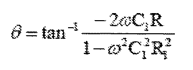
図1A、図1Bに記載されたフェーズシフタの変形例を、それぞれ図2A、図2Bを用いて説明する。図1A、図1Bのフェーズシフタ1100に対して、図2A、図2Bのフェーズシフタ1200は、トランジスタTr2及び容量素子C2が追加された構成である。なお図2A、図2Bにおいて、図4と同じ場所の抵抗素子には図4と同じ符号を付している。
図2A、図2Bに記載されたフェーズシフタの変形例を、それぞれ図3A、図3Bを用いて説明する。図3A、図3Bは負帰還側の抵抗素子にもトランジスタを用いた構成例である。すなわち、図3A、図3Bのフェーズシフタ1300は、図2A、図2Bそれぞれに対してトランジスタTr3乃至トランジスタTr5及び容量素子C3が追加されたものである。
半導体装置の断面構造の一部を図5に示す。図5に示す半導体装置は、トランジスタ550と、トランジスタ500と、容量素子600と、を有し、これらが順に積層している例であって、このような積層構造によってフェーズシフタ等の半導体装置を小型化することができる。トランジスタ500はバックゲート端子として機能する導電体592と、ゲート端子として機能する導電体593を有する。バックゲート端子として機能する導電体592は省略することが可能である。
図7A乃至図7Bには、上記トランジスタ500の変形例を示し、図7Cには、上記トランジスタ550の変形例を示す。図7Aはトランジスタ500のチャネル長方向の断面図であり、図7Bはトランジスタ500のチャネル幅方向の断面図である。
図8A、図8B、および図8Cに示すトランジスタ500Aは、図7A、図7Bに示す構成のトランジスタ500の変形例である。図8Aはトランジスタ500Aの上面図であり、図8Bはトランジスタ500Aのチャネル長方向の断面図であり、図8Cはトランジスタ500Aのチャネル幅方向の断面図である。なお、図8Aの上面図では、図の明瞭化のために一部の要素の記載を省略している。図8A、図8B、および図8Cに示す構成は、トランジスタ550等、本発明の一態様の半導体装置が有する他のトランジスタにも適用することができる。
図9A、図9Bおよび図9Cを用いて、トランジスタ500Bの構成例を説明する。図9Aはトランジスタ500Bの上面図である。図9Bは、図9Aに一点鎖線で示すL1−L2部位の断面図である。図9Cは、図9Aに一点鎖線で示すW1−W2部位の断面図である。なお、図9Aの上面図では、図の明瞭化のために一部の要素の記載を省略している。
本実施の形態では、金属酸化物の一種である酸化物半導体について説明する。
まず、酸化物半導体における、結晶構造の分類について、図10Aを用いて説明を行う。図10Aは、酸化物半導体、代表的にはIGZO(Inと、Gaと、Znと、を含む金属酸化物)の結晶構造の分類を説明する図である。
なお、酸化物半導体は、結晶構造に着目した場合、図10Aとは異なる分類となる場合がある。例えば、酸化物半導体は、単結晶酸化物半導体と、それ以外の非単結晶酸化物半導体と、に分けられる。非単結晶酸化物半導体としては、例えば、上述のCAAC−OS、及びnc−OSがある。また、非単結晶酸化物半導体には、多結晶酸化物半導体、擬似非晶質酸化物半導体(a−like OS:amorphous−like oxide semiconductor)、非晶質酸化物半導体、などが含まれる。
CAAC−OSは、複数の結晶領域を有し、当該複数の結晶領域はc軸が特定の方向に配向している酸化物半導体である。なお、特定の方向とは、CAAC−OS膜の厚さ方向、CAAC−OS膜の被形成面の法線方向、またはCAAC−OS膜の表面の法線方向である。また、結晶領域とは、原子配列に周期性を有する領域である。なお、原子配列を格子配列とみなすと、結晶領域とは、格子配列の揃った領域でもある。さらに、CAAC−OSは、a−b面方向において複数の結晶領域が連結する領域を有し、当該領域は歪みを有する場合がある。なお、歪みとは、複数の結晶領域が連結する領域において、格子配列の揃った領域と、別の格子配列の揃った領域と、の間で格子配列の向きが変化している箇所を指す。つまり、CAAC−OSは、c軸配向し、a−b面方向には明らかな配向をしていない酸化物半導体である。
nc−OSは、微小な領域(例えば、1nm以上10nm以下の領域、特に1nm以上3nm以下の領域)において原子配列に周期性を有する。別言すると、nc−OSは、微小な結晶を有する。なお、当該微小な結晶の大きさは、例えば、1nm以上10nm以下、特に1nm以上3nm以下であることから、当該微小な結晶をナノ結晶ともいう。また、nc−OSは、異なるナノ結晶間で結晶方位に規則性が見られない。そのため、膜全体で配向性が見られない。したがって、nc−OSは、分析方法によっては、a−like OSや非晶質酸化物半導体と区別が付かない場合がある。例えば、nc−OS膜に対し、XRD装置を用いて構造解析を行うと、θ/2θスキャンを用いたOut−of−plane XRD測定では、結晶性を示すピークが検出されない。また、nc−OS膜に対し、ナノ結晶よりも大きいプローブ径(例えば50nm以上)の電子線を用いる電子線回折(制限視野電子線回折ともいう。)を行うと、ハローパターンのような回折パターンが観測される。一方、nc−OS膜に対し、ナノ結晶の大きさと近いかナノ結晶より小さいプローブ径(例えば1nm以上30nm以下)の電子線を用いる電子線回折(ナノビーム電子線回折ともいう。)を行うと、ダイレクトスポットを中心とするリング状の領域内に複数のスポットが観測される電子線回折パターンが取得される場合がある。
a−like OSは、nc−OSと非晶質酸化物半導体との間の構造を有する酸化物半導体である。a−like OSは、鬆又は低密度領域を有する。即ち、a−like OSは、nc−OS及びCAAC−OSと比べて、結晶性が低い。また、a−like OSは、nc−OS及びCAAC−OSと比べて、膜中の水素濃度が高い。
次に、上述のCAC−OSの詳細について、説明を行う。なお、CAC−OSは材料構成に関する。
CAC−OSとは、例えば、金属酸化物を構成する元素が、0.5nm以上10nm以下、好ましくは、1nm以上3nm以下、またはその近傍のサイズで偏在した材料の一構成である。なお、以下では、金属酸化物において、一つまたは複数の金属元素が偏在し、該金属元素を有する領域が、0.5nm以上10nm以下、好ましくは、1nm以上3nm以下、またはその近傍のサイズで混合した状態をモザイク状、またはパッチ状ともいう。
続いて、上記酸化物半導体をトランジスタに用いる場合について説明する。
ここで、酸化物半導体中における各不純物の影響について説明する。
本実施の形態では上述した半導体装置の応用例について説明する。
図11Aは、ダイシング処理が行なわれる前の基板711の上面図を示している。基板711としては、例えば、半導体基板(「半導体ウエハ」ともいう。)を用いることができる。基板711上には、複数の回路領域712が設けられている。回路領域712には、本発明の一態様に係る半導体装置や、CPU、RFタグ、またはイメージセンサなどを設けることができる。
チップ715を電子部品に適用する例について、図12Aおよび図12Bを用いて説明する。なお、電子部品は、半導体パッケージ、またはIC用パッケージともいう。電子部品は、端子取り出し方向や、端子の形状に応じて、複数の規格や名称が存在する。
次に、本発明の一態様に係る半導体装置または上記電子部品を備えた電子機器の例について図13および図14A乃至図14Fを用いて説明を行う。
本明細書などに示したOSトランジスタを用いて、ノーマリーオフCPU(「Noff−CPU」ともいう。)を実現することができる。なお、Noff−CPUとは、ゲート電圧が0Vであっても非導通状態(オフ状態ともいう)であるノーマリーオフ型のトランジスタを含む集積回路である。
Claims (4)
- フェーズシフタの入力端子と、フェーズシフタの出力端子との間に、オペアンプを有し、
前記オペアンプの第1の入力端子と電気的に接続された、トランジスタと、
前記オペアンプの第2の入力端子と電気的に接続された、第1の抵抗素子と、
前記オペアンプの第2の入力端子と電気的に接続された、第2の抵抗素子と、を有し、
前記トランジスタのゲートは、第1の端子と電気的に接続され、
前記トランジスタのソースまたはドレインの一方は、前記フェーズシフタの入力端子と電気的に接続され、
前記トランジスタのソースまたはドレインの他方は、前記オペアンプの第1の入力端子と電気的に接続され、
前記第1の抵抗素子は、前記フェーズシフタの入力端子と電気的に接続され、
前記第2の抵抗素子は、前記フェーズシフタの出力端子と電気的に接続され、
少なくとも前記オペアンプが有するトランジスタは、前記トランジスタと重なる領域を有する、
半導体装置。 - フェーズシフタの入力端子と、フェーズシフタの出力端子との間に、オペアンプを有し、
前記オペアンプの第1の入力端子と電気的に接続された、トランジスタと、
前記トランジスタのソースまたはドレインの他方と電気的に接続された、容量素子と、
前記オペアンプの第2の入力端子と電気的に接続された、第1の抵抗素子と、
前記オペアンプの第2の入力端子と電気的に接続された、第2の抵抗素子と、を有し、
前記トランジスタのゲートは、第1の端子と電気的に接続され、
前記トランジスタのソースまたはドレインの一方は、前記フェーズシフタの入力端子と電気的に接続され、
前記トランジスタのソースまたはドレインの他方は、前記オペアンプの第1の入力端子と電気的に接続され、
前記第1の抵抗素子は、前記フェーズシフタの入力端子と電気的に接続され、
前記第2の抵抗素子は、前記フェーズシフタの出力端子と電気的に接続され、
少なくとも前記オペアンプが有するトランジスタは、前記トランジスタと重なる領域を有する、
半導体装置。 - フェーズシフタの入力端子と、フェーズシフタの出力端子との間に、オペアンプを有し、
前記オペアンプの第1の入力端子と電気的に接続された、トランジスタと、
前記トランジスタのゲートと電気的に接続された、記憶素子と、
前記オペアンプの第2の入力端子と電気的に接続された、第1の抵抗素子と、
前記オペアンプの第2の入力端子と電気的に接続された、第2の抵抗素子とを有し、
前記トランジスタのゲートは、第1の端子と電気的に接続され、
前記トランジスタのソースまたはドレインの一方は、前記フェーズシフタの入力端子と電気的に接続され、
前記トランジスタのソースまたはドレインの他方は、前記オペアンプの第1の入力端子と電気的に接続され、
前記第1の抵抗素子は、前記フェーズシフタの入力端子と電気的に接続され、
前記第2の抵抗素子は、前記フェーズシフタの出力端子と電気的に接続され、
少なくとも前記オペアンプが有するトランジスタは、前記トランジスタと重なる領域を有する、
半導体装置。 - 請求項3において、
前記記憶素子は、第1のトランジスタ及び第1の容量素子を有し、
前記第1のトランジスタは、酸化物半導体膜を有し、
少なくとも前記オペアンプが有するトランジスタは、前記第1のトランジスタと重なる領域を有する、
半導体装置。
Priority Applications (4)
| Application Number | Priority Date | Filing Date | Title |
|---|---|---|---|
| CN202080038462.6A CN113950740A (zh) | 2019-06-07 | 2020-05-22 | 半导体装置 |
| KR1020227000157A KR102849048B1 (ko) | 2019-06-07 | 2020-05-22 | 반도체 장치 |
| JP2021524489A JP7536759B2 (ja) | 2019-06-07 | 2020-05-22 | 半導体装置 |
| US17/614,690 US12101067B2 (en) | 2019-06-07 | 2020-05-22 | Semiconductor device |
Applications Claiming Priority (2)
| Application Number | Priority Date | Filing Date | Title |
|---|---|---|---|
| JP2019106670 | 2019-06-07 | ||
| JP2019-106670 | 2019-06-07 |
Publications (1)
| Publication Number | Publication Date |
|---|---|
| WO2020245693A1 true WO2020245693A1 (ja) | 2020-12-10 |
Family
ID=73652486
Family Applications (1)
| Application Number | Title | Priority Date | Filing Date |
|---|---|---|---|
| PCT/IB2020/054867 Ceased WO2020245693A1 (ja) | 2019-06-07 | 2020-05-22 | 半導体装置 |
Country Status (5)
| Country | Link |
|---|---|
| US (1) | US12101067B2 (ja) |
| JP (1) | JP7536759B2 (ja) |
| KR (1) | KR102849048B1 (ja) |
| CN (1) | CN113950740A (ja) |
| WO (1) | WO2020245693A1 (ja) |
Families Citing this family (1)
| Publication number | Priority date | Publication date | Assignee | Title |
|---|---|---|---|---|
| CN113875152A (zh) | 2019-05-24 | 2021-12-31 | 株式会社半导体能源研究所 | 半导体装置及电子设备 |
Citations (5)
| Publication number | Priority date | Publication date | Assignee | Title |
|---|---|---|---|---|
| JP2013235564A (ja) * | 2012-04-11 | 2013-11-21 | Semiconductor Energy Lab Co Ltd | 半導体装置 |
| JP2015043686A (ja) * | 2013-07-26 | 2015-03-05 | 株式会社半導体エネルギー研究所 | Dcdcコンバータ |
| JP2015079944A (ja) * | 2013-09-10 | 2015-04-23 | 株式会社半導体エネルギー研究所 | 半導体装置 |
| JP2015181081A (ja) * | 2014-03-07 | 2015-10-15 | 株式会社半導体エネルギー研究所 | 半導体装置および電子機器 |
| JP2017117508A (ja) * | 2015-12-22 | 2017-06-29 | 株式会社半導体エネルギー研究所 | 半導体装置、表示パネル、及び電子機器 |
Family Cites Families (10)
| Publication number | Priority date | Publication date | Assignee | Title |
|---|---|---|---|---|
| US4249128A (en) * | 1978-02-06 | 1981-02-03 | White's Electronics, Inc. | Wide pulse gated metal detector with improved noise rejection |
| KR960027857A (ko) * | 1994-12-07 | 1996-07-22 | 양승택 | 위상편이변조용 변조기 회로 |
| TW379479B (en) * | 1996-03-12 | 2000-01-11 | Tif Co Ltd | Tuned amplifier |
| US6646508B1 (en) * | 1996-12-30 | 2003-11-11 | Anthony T. Barbetta | Wide bandwidth, current sharing, MOSFET audio power amplifier with multiple feedback loops |
| KR100795934B1 (ko) * | 2005-04-29 | 2008-01-22 | 최대섭 | 태양광 인버터용 자동위상 변환 및 보호 회로 |
| US8451071B2 (en) * | 2008-11-24 | 2013-05-28 | Raytheon Company | Low noise oscillators |
| KR20150104518A (ko) | 2014-03-05 | 2015-09-15 | 가부시키가이샤 한도오따이 에네루기 켄큐쇼 | 레벨 시프터 회로 |
| JP6582640B2 (ja) * | 2015-07-07 | 2019-10-02 | 住友電気工業株式会社 | レーザ駆動回路 |
| JP6689712B2 (ja) | 2016-08-23 | 2020-04-28 | ルネサスエレクトロニクス株式会社 | レゾルバ補正装置及び半導体装置 |
| TWI687054B (zh) * | 2018-07-20 | 2020-03-01 | 茂達電子股份有限公司 | 多通道系統的相移控制電路 |
-
2020
- 2020-05-22 US US17/614,690 patent/US12101067B2/en active Active
- 2020-05-22 CN CN202080038462.6A patent/CN113950740A/zh active Pending
- 2020-05-22 WO PCT/IB2020/054867 patent/WO2020245693A1/ja not_active Ceased
- 2020-05-22 KR KR1020227000157A patent/KR102849048B1/ko active Active
- 2020-05-22 JP JP2021524489A patent/JP7536759B2/ja active Active
Patent Citations (5)
| Publication number | Priority date | Publication date | Assignee | Title |
|---|---|---|---|---|
| JP2013235564A (ja) * | 2012-04-11 | 2013-11-21 | Semiconductor Energy Lab Co Ltd | 半導体装置 |
| JP2015043686A (ja) * | 2013-07-26 | 2015-03-05 | 株式会社半導体エネルギー研究所 | Dcdcコンバータ |
| JP2015079944A (ja) * | 2013-09-10 | 2015-04-23 | 株式会社半導体エネルギー研究所 | 半導体装置 |
| JP2015181081A (ja) * | 2014-03-07 | 2015-10-15 | 株式会社半導体エネルギー研究所 | 半導体装置および電子機器 |
| JP2017117508A (ja) * | 2015-12-22 | 2017-06-29 | 株式会社半導体エネルギー研究所 | 半導体装置、表示パネル、及び電子機器 |
Also Published As
| Publication number | Publication date |
|---|---|
| JP7536759B2 (ja) | 2024-08-20 |
| US12101067B2 (en) | 2024-09-24 |
| US20220231644A1 (en) | 2022-07-21 |
| KR20220017998A (ko) | 2022-02-14 |
| CN113950740A (zh) | 2022-01-18 |
| JPWO2020245693A1 (ja) | 2020-12-10 |
| KR102849048B1 (ko) | 2025-08-22 |
Similar Documents
| Publication | Publication Date | Title |
|---|---|---|
| JP7769155B2 (ja) | 半導体装置 | |
| JP7615027B2 (ja) | 半導体装置、無線通信装置 | |
| JP7725364B2 (ja) | 半導体装置および電子機器 | |
| JP2025100582A (ja) | 通信装置 | |
| JP7585200B2 (ja) | 周波数電圧変換回路、または発振器 | |
| JP7745071B2 (ja) | 半導体装置 | |
| JP7646558B2 (ja) | 半導体装置 | |
| US11948945B2 (en) | Semiconductor device and wireless communication device with the semiconductor device | |
| JP7704677B2 (ja) | 通信装置 | |
| WO2021229385A1 (ja) | 半導体装置 | |
| JP2025019138A (ja) | 半導体装置 | |
| WO2020240340A1 (ja) | 半導体装置 | |
| JP7536759B2 (ja) | 半導体装置 | |
| WO2020261039A1 (ja) | 高周波増幅回路を有する半導体装置、電子部品、および電子機器 |
Legal Events
| Date | Code | Title | Description |
|---|---|---|---|
| 121 | Ep: the epo has been informed by wipo that ep was designated in this application |
Ref document number: 20819183 Country of ref document: EP Kind code of ref document: A1 |
|
| ENP | Entry into the national phase |
Ref document number: 2021524489 Country of ref document: JP Kind code of ref document: A |
|
| NENP | Non-entry into the national phase |
Ref country code: DE |
|
| ENP | Entry into the national phase |
Ref document number: 20227000157 Country of ref document: KR Kind code of ref document: A |
|
| 122 | Ep: pct application non-entry in european phase |
Ref document number: 20819183 Country of ref document: EP Kind code of ref document: A1 |