WO2020241528A1 - 液晶表示装置 - Google Patents
液晶表示装置 Download PDFInfo
- Publication number
- WO2020241528A1 WO2020241528A1 PCT/JP2020/020419 JP2020020419W WO2020241528A1 WO 2020241528 A1 WO2020241528 A1 WO 2020241528A1 JP 2020020419 W JP2020020419 W JP 2020020419W WO 2020241528 A1 WO2020241528 A1 WO 2020241528A1
- Authority
- WO
- WIPO (PCT)
- Prior art keywords
- region
- insulating layer
- substrate
- layer
- liquid crystal
- Prior art date
- Legal status (The legal status is an assumption and is not a legal conclusion. Google has not performed a legal analysis and makes no representation as to the accuracy of the status listed.)
- Ceased
Links
Images




Classifications
-
- G—PHYSICS
- G02—OPTICS
- G02F—OPTICAL DEVICES OR ARRANGEMENTS FOR THE CONTROL OF LIGHT BY MODIFICATION OF THE OPTICAL PROPERTIES OF THE MEDIA OF THE ELEMENTS INVOLVED THEREIN; NON-LINEAR OPTICS; FREQUENCY-CHANGING OF LIGHT; OPTICAL LOGIC ELEMENTS; OPTICAL ANALOGUE/DIGITAL CONVERTERS
- G02F1/00—Devices or arrangements for the control of the intensity, colour, phase, polarisation or direction of light arriving from an independent light source, e.g. switching, gating or modulating; Non-linear optics
- G02F1/01—Devices or arrangements for the control of the intensity, colour, phase, polarisation or direction of light arriving from an independent light source, e.g. switching, gating or modulating; Non-linear optics for the control of the intensity, phase, polarisation or colour
- G02F1/13—Devices or arrangements for the control of the intensity, colour, phase, polarisation or direction of light arriving from an independent light source, e.g. switching, gating or modulating; Non-linear optics for the control of the intensity, phase, polarisation or colour based on liquid crystals, e.g. single liquid crystal display cells
- G02F1/133—Constructional arrangements; Operation of liquid crystal cells; Circuit arrangements
- G02F1/1333—Constructional arrangements; Manufacturing methods
- G02F1/1339—Gaskets; Spacers; Sealing of cells
- G02F1/13394—Gaskets; Spacers; Sealing of cells spacers regularly patterned on the cell subtrate, e.g. walls, pillars
-
- G—PHYSICS
- G02—OPTICS
- G02F—OPTICAL DEVICES OR ARRANGEMENTS FOR THE CONTROL OF LIGHT BY MODIFICATION OF THE OPTICAL PROPERTIES OF THE MEDIA OF THE ELEMENTS INVOLVED THEREIN; NON-LINEAR OPTICS; FREQUENCY-CHANGING OF LIGHT; OPTICAL LOGIC ELEMENTS; OPTICAL ANALOGUE/DIGITAL CONVERTERS
- G02F1/00—Devices or arrangements for the control of the intensity, colour, phase, polarisation or direction of light arriving from an independent light source, e.g. switching, gating or modulating; Non-linear optics
- G02F1/01—Devices or arrangements for the control of the intensity, colour, phase, polarisation or direction of light arriving from an independent light source, e.g. switching, gating or modulating; Non-linear optics for the control of the intensity, phase, polarisation or colour
- G02F1/13—Devices or arrangements for the control of the intensity, colour, phase, polarisation or direction of light arriving from an independent light source, e.g. switching, gating or modulating; Non-linear optics for the control of the intensity, phase, polarisation or colour based on liquid crystals, e.g. single liquid crystal display cells
- G02F1/133—Constructional arrangements; Operation of liquid crystal cells; Circuit arrangements
- G02F1/1333—Constructional arrangements; Manufacturing methods
- G02F1/133345—Insulating layers
-
- G—PHYSICS
- G02—OPTICS
- G02F—OPTICAL DEVICES OR ARRANGEMENTS FOR THE CONTROL OF LIGHT BY MODIFICATION OF THE OPTICAL PROPERTIES OF THE MEDIA OF THE ELEMENTS INVOLVED THEREIN; NON-LINEAR OPTICS; FREQUENCY-CHANGING OF LIGHT; OPTICAL LOGIC ELEMENTS; OPTICAL ANALOGUE/DIGITAL CONVERTERS
- G02F1/00—Devices or arrangements for the control of the intensity, colour, phase, polarisation or direction of light arriving from an independent light source, e.g. switching, gating or modulating; Non-linear optics
- G02F1/01—Devices or arrangements for the control of the intensity, colour, phase, polarisation or direction of light arriving from an independent light source, e.g. switching, gating or modulating; Non-linear optics for the control of the intensity, phase, polarisation or colour
- G02F1/13—Devices or arrangements for the control of the intensity, colour, phase, polarisation or direction of light arriving from an independent light source, e.g. switching, gating or modulating; Non-linear optics for the control of the intensity, phase, polarisation or colour based on liquid crystals, e.g. single liquid crystal display cells
- G02F1/133—Constructional arrangements; Operation of liquid crystal cells; Circuit arrangements
- G02F1/1333—Constructional arrangements; Manufacturing methods
- G02F1/13338—Input devices, e.g. touch panels
-
- G—PHYSICS
- G02—OPTICS
- G02F—OPTICAL DEVICES OR ARRANGEMENTS FOR THE CONTROL OF LIGHT BY MODIFICATION OF THE OPTICAL PROPERTIES OF THE MEDIA OF THE ELEMENTS INVOLVED THEREIN; NON-LINEAR OPTICS; FREQUENCY-CHANGING OF LIGHT; OPTICAL LOGIC ELEMENTS; OPTICAL ANALOGUE/DIGITAL CONVERTERS
- G02F1/00—Devices or arrangements for the control of the intensity, colour, phase, polarisation or direction of light arriving from an independent light source, e.g. switching, gating or modulating; Non-linear optics
- G02F1/01—Devices or arrangements for the control of the intensity, colour, phase, polarisation or direction of light arriving from an independent light source, e.g. switching, gating or modulating; Non-linear optics for the control of the intensity, phase, polarisation or colour
- G02F1/13—Devices or arrangements for the control of the intensity, colour, phase, polarisation or direction of light arriving from an independent light source, e.g. switching, gating or modulating; Non-linear optics for the control of the intensity, phase, polarisation or colour based on liquid crystals, e.g. single liquid crystal display cells
- G02F1/133—Constructional arrangements; Operation of liquid crystal cells; Circuit arrangements
- G02F1/1333—Constructional arrangements; Manufacturing methods
- G02F1/133388—Constructional arrangements; Manufacturing methods with constructional differences between the display region and the peripheral region
-
- G—PHYSICS
- G02—OPTICS
- G02F—OPTICAL DEVICES OR ARRANGEMENTS FOR THE CONTROL OF LIGHT BY MODIFICATION OF THE OPTICAL PROPERTIES OF THE MEDIA OF THE ELEMENTS INVOLVED THEREIN; NON-LINEAR OPTICS; FREQUENCY-CHANGING OF LIGHT; OPTICAL LOGIC ELEMENTS; OPTICAL ANALOGUE/DIGITAL CONVERTERS
- G02F1/00—Devices or arrangements for the control of the intensity, colour, phase, polarisation or direction of light arriving from an independent light source, e.g. switching, gating or modulating; Non-linear optics
- G02F1/01—Devices or arrangements for the control of the intensity, colour, phase, polarisation or direction of light arriving from an independent light source, e.g. switching, gating or modulating; Non-linear optics for the control of the intensity, phase, polarisation or colour
- G02F1/13—Devices or arrangements for the control of the intensity, colour, phase, polarisation or direction of light arriving from an independent light source, e.g. switching, gating or modulating; Non-linear optics for the control of the intensity, phase, polarisation or colour based on liquid crystals, e.g. single liquid crystal display cells
- G02F1/133—Constructional arrangements; Operation of liquid crystal cells; Circuit arrangements
- G02F1/1333—Constructional arrangements; Manufacturing methods
- G02F1/1335—Structural association of cells with optical devices, e.g. polarisers or reflectors
- G02F1/133509—Filters, e.g. light shielding masks
- G02F1/133512—Light shielding layers, e.g. black matrix
-
- G—PHYSICS
- G02—OPTICS
- G02F—OPTICAL DEVICES OR ARRANGEMENTS FOR THE CONTROL OF LIGHT BY MODIFICATION OF THE OPTICAL PROPERTIES OF THE MEDIA OF THE ELEMENTS INVOLVED THEREIN; NON-LINEAR OPTICS; FREQUENCY-CHANGING OF LIGHT; OPTICAL LOGIC ELEMENTS; OPTICAL ANALOGUE/DIGITAL CONVERTERS
- G02F1/00—Devices or arrangements for the control of the intensity, colour, phase, polarisation or direction of light arriving from an independent light source, e.g. switching, gating or modulating; Non-linear optics
- G02F1/01—Devices or arrangements for the control of the intensity, colour, phase, polarisation or direction of light arriving from an independent light source, e.g. switching, gating or modulating; Non-linear optics for the control of the intensity, phase, polarisation or colour
- G02F1/13—Devices or arrangements for the control of the intensity, colour, phase, polarisation or direction of light arriving from an independent light source, e.g. switching, gating or modulating; Non-linear optics for the control of the intensity, phase, polarisation or colour based on liquid crystals, e.g. single liquid crystal display cells
- G02F1/133—Constructional arrangements; Operation of liquid crystal cells; Circuit arrangements
- G02F1/1333—Constructional arrangements; Manufacturing methods
- G02F1/1339—Gaskets; Spacers; Sealing of cells
- G02F1/13392—Gaskets; Spacers; Sealing of cells spacers dispersed on the cell substrate, e.g. spherical particles, microfibres
-
- G—PHYSICS
- G02—OPTICS
- G02F—OPTICAL DEVICES OR ARRANGEMENTS FOR THE CONTROL OF LIGHT BY MODIFICATION OF THE OPTICAL PROPERTIES OF THE MEDIA OF THE ELEMENTS INVOLVED THEREIN; NON-LINEAR OPTICS; FREQUENCY-CHANGING OF LIGHT; OPTICAL LOGIC ELEMENTS; OPTICAL ANALOGUE/DIGITAL CONVERTERS
- G02F1/00—Devices or arrangements for the control of the intensity, colour, phase, polarisation or direction of light arriving from an independent light source, e.g. switching, gating or modulating; Non-linear optics
- G02F1/01—Devices or arrangements for the control of the intensity, colour, phase, polarisation or direction of light arriving from an independent light source, e.g. switching, gating or modulating; Non-linear optics for the control of the intensity, phase, polarisation or colour
- G02F1/13—Devices or arrangements for the control of the intensity, colour, phase, polarisation or direction of light arriving from an independent light source, e.g. switching, gating or modulating; Non-linear optics for the control of the intensity, phase, polarisation or colour based on liquid crystals, e.g. single liquid crystal display cells
- G02F1/133—Constructional arrangements; Operation of liquid crystal cells; Circuit arrangements
- G02F1/1333—Constructional arrangements; Manufacturing methods
- G02F1/1339—Gaskets; Spacers; Sealing of cells
- G02F1/13396—Spacers having different sizes
-
- G—PHYSICS
- G02—OPTICS
- G02F—OPTICAL DEVICES OR ARRANGEMENTS FOR THE CONTROL OF LIGHT BY MODIFICATION OF THE OPTICAL PROPERTIES OF THE MEDIA OF THE ELEMENTS INVOLVED THEREIN; NON-LINEAR OPTICS; FREQUENCY-CHANGING OF LIGHT; OPTICAL LOGIC ELEMENTS; OPTICAL ANALOGUE/DIGITAL CONVERTERS
- G02F1/00—Devices or arrangements for the control of the intensity, colour, phase, polarisation or direction of light arriving from an independent light source, e.g. switching, gating or modulating; Non-linear optics
- G02F1/01—Devices or arrangements for the control of the intensity, colour, phase, polarisation or direction of light arriving from an independent light source, e.g. switching, gating or modulating; Non-linear optics for the control of the intensity, phase, polarisation or colour
- G02F1/13—Devices or arrangements for the control of the intensity, colour, phase, polarisation or direction of light arriving from an independent light source, e.g. switching, gating or modulating; Non-linear optics for the control of the intensity, phase, polarisation or colour based on liquid crystals, e.g. single liquid crystal display cells
- G02F1/133—Constructional arrangements; Operation of liquid crystal cells; Circuit arrangements
- G02F1/1333—Constructional arrangements; Manufacturing methods
- G02F1/1343—Electrodes
- G02F1/13439—Electrodes characterised by their electrical, optical, physical properties; materials therefor; method of making
-
- G—PHYSICS
- G09—EDUCATION; CRYPTOGRAPHY; DISPLAY; ADVERTISING; SEALS
- G09F—DISPLAYING; ADVERTISING; SIGNS; LABELS OR NAME-PLATES; SEALS
- G09F9/00—Indicating arrangements for variable information in which the information is built-up on a support by selection or combination of individual elements
- G09F9/30—Indicating arrangements for variable information in which the information is built-up on a support by selection or combination of individual elements in which the desired character or characters are formed by combining individual elements
Definitions
- An embodiment of the present invention relates to a liquid crystal display device.
- a liquid crystal display device having a light-shielding portion between the image display unit and the transparent display unit is disclosed.
- a liquid crystal display device having a display unit and a transparent unit overlapping the camera is disclosed.
- An object of the present embodiment is to provide a liquid crystal display device capable of improving the yield of products.
- the liquid crystal display device is A first substrate, a second substrate, a facing region where the first substrate and the second substrate face each other, a liquid crystal layer and a first spacer located between the first substrate and the second substrate, and the like.
- the facing region is located between a first region for displaying an image, a second region located inside the first region in a plan view, and the first region and the second region.
- the second substrate includes a frame-shaped frame region surrounding the second region, the second substrate includes a light-shielding layer formed in the frame region in a plan view, and the second region is more transparent than the first region. It is a high region, the liquid crystal layer is located in the second region, the frame region and the first region, the first spacer is located in the second region, and the first substrate or the second substrate is located. It is provided in.
- FIG. 1 is a cross-sectional view of the liquid crystal display device of one embodiment.
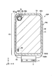
- FIG. 2 is a plan view of the liquid crystal display device shown in FIG.
- FIG. 3 is a diagram showing a basic structure and an equivalent circuit of the pixels shown in FIG.
- FIG. 4 is a cross-sectional view showing a configuration example of the liquid crystal display device shown in FIG.
- FIG. 5 is a plan view showing a configuration example of a touch sensor included in the liquid crystal display device shown in FIG.
- FIG. 6 is an enlarged plan view of the window area shown in FIG.
- FIG. 7 is a cross-sectional view of the liquid crystal display device along the line AB shown in FIG.
- FIG. 8 is a plan view of the liquid crystal display device, and is a diagram for explaining the positional relationship of each spacer.
- FIG. 9 is a cross-sectional view showing a modified example of the liquid crystal display device shown in FIG. 7.
- FIG. 1 is a cross-sectional view of the liquid crystal display device DSP of one embodiment.
- the first direction X, the second direction Y, and the third direction Z are orthogonal to each other, but may intersect at an angle other than 90 degrees.
- the position on the tip end side of the arrow indicating the third direction Z is referred to as an upper position, and the position opposite to the tip end of the arrow is referred to as a lower position.
- viewing from top to bottom toward the XY plane defined by the first direction X and the second direction Y is referred to as plan view.
- the liquid crystal display device DSP includes a transparent substrate CG, a display panel PNL, a lighting device IL, and an electronic component PA.
- the transparent substrate CG, the display panel PNL, and the electronic component PA are arranged in this order along the third direction Z.
- the display panel PNL includes a first substrate SUB1, a second substrate SUB2, an optical element OD1, and an optical element OD2.
- the second substrate SUB2 includes a light-shielding layer BMP.
- the light-shielding layer BMP is located between the first substrate SUB1 and the second substrate SUB2.
- the optical element OD1 including the polarizing plate PL1 is adhered to the first substrate SUB1.
- the optical element OD2 including the polarizing plate PL2 is adhered to the second substrate SUB2.
- the optical elements OD1 and OD2 each have a through hole at a position overlapping the electronic component PA in the third direction Z.
- the optical elements OD1 and OD2 may be provided with a retardation plate, a diffusion layer, an antireflection layer, and the like, if necessary.
- the transparent substrate CG is adhered to the display panel PNL by the transparent adhesive layer AD.
- the transparent substrate CG includes a light-shielding layer BMC.
- the light-shielding layer BMC is provided on the lower surface of the transparent substrate CG and overlaps the light-shielding layer BMP in the third direction Z.
- the transparent substrate CG is a glass substrate, a flexible resin substrate, or the like.
- the lighting device IL illuminates the display panel PNL.
- the illuminator IL has a through hole TH that overlaps the electronic component PA in the third direction Z.
- the electronic component PA is a light receiving element PA in this embodiment, and the light receiving element PA is a camera as an example.
- the light receiving element PA includes a device that detects visible light, a device that detects infrared rays, a proximity sensor that senses the proximity of a detection target object, a detection element that detects infrared rays reflected from the detection target object, and the like. It may be a combination of each.
- the light receiving element PA is inserted into the through hole TH of the lighting device IL.
- the light receiving element PA receives light in the third direction Z via the transparent substrate CG, the transparent adhesive layer AD, or the display panel PNL.
- FIG. 2 is a plan view of the liquid crystal display device DSP shown in FIG. As shown in FIG. 2, the liquid crystal display device DSP further includes a wiring board F1 and an IC chip 1.
- the display panel PNL has an opposite region FA and an extension region EA arranged along the second direction Y.
- the facing region FA is a region in which the first substrate SUB1 and the second substrate SUB2 face each other and overlap each other, and is two portions of the display panel PNL.
- the extension area EA can also be said to be one portion of the display panel PNL in which the first substrate SUB1 is exposed from the second substrate SUB2.
- the facing area FA includes a display area DA for displaying an image, a frame-shaped non-display area NDA surrounding the display area DA, a window area WA, and a frame area FRA.
- the window area WA is located inside the display area DA in a plan view.
- the window region WA is a perfect circle, but it may be another circle such as an ellipse or a polygon other than a circle.
- the frame area FRA is a frame-shaped area located between the display area DA and the window area WA and surrounding the window area WA.
- the display area DA may be referred to as a first area
- the window area WA may be referred to as a second area.
- a plurality of pixels PX arranged in a matrix (matrix) in the first direction (row direction) X and the second direction (column direction) Y are located.
- the pixel PX is not provided in the window area WA and the frame area FRA.
- the pixel PX here indicates a minimum unit that can be individually controlled according to a pixel signal, and may be referred to as a sub-pixel.
- the pixel PX is, for example, either a red pixel exhibiting red, a green pixel exhibiting green, a blue pixel exhibiting blue, or a white pixel exhibiting white.
- the light receiving element PA is located inside the window region WA in a plan view.
- the through hole TH shown in FIG. 1 overlaps the window region WA.
- the light-shielding layer BMP is provided over the entire frame region FRA.
- the light-shielding layer BMP has an inner surface BI and an outer surface BO.
- the inner surface BI corresponds to the boundary between the window area WA and the frame area FRA
- the outer surface BO corresponds to the boundary between the frame area FRA and the display area DA.
- the IC chip 1 and the wiring board F1 may read a signal from the display panel PNL, but mainly function as a signal source for supplying a signal to the display panel PNL.
- the IC chip 1 is mounted on the wiring board F1 and is electrically connected to the wiring board F1.
- the IC chip 1 may be mounted on the extension area EA and electrically connected to the extension area EA.
- the IC chip 1 has a built-in display driver DD that outputs a signal required for image display in an image display mode for displaying an image. Further, in the illustrated example, the IC chip 1 has a built-in touch controller TCN that controls a touch sensing mode for detecting the approach or contact of an object with the liquid crystal display device DSP. In the figure, the display driver DD and the touch controller TCN are shown by dotted lines.
- the wiring board F1 is a bendable flexible printed circuit board.
- the display panel PNL further includes a liquid crystal layer LC and a seal SE.
- the seal SE is located in the non-display area NDA and joins the first substrate SUB1 and the second substrate SUB2.
- the liquid crystal layer LC is held between the first substrate SUB1 and the second substrate SUB2, and is sealed by the seal SE.
- the liquid crystal layer LC is provided over each of the window area WA, the frame area FRA, and the display area DA. In FIG. 2, the liquid crystal layer LC and the seal SE are shown by different diagonal lines.
- the display panel PNL has a display mode using a lateral electric field along the main surface of the substrate and a vertical electric field along the normal of the main surface of the substrate. It corresponds to the display mode to be used, the display mode to use the gradient electric field inclined in the diagonal direction with respect to the main surface of the substrate, and the display mode to use the above-mentioned lateral electric field, longitudinal electric field, and gradient electric field in an appropriate combination. Any configuration may be provided.
- the substrate main surface here is a surface parallel to the XY plane defined by the first direction X and the second direction Y.
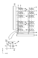
- FIG. 3 is a diagram showing a basic structure and an equivalent circuit of the pixels shown in FIG.
- the plurality of scanning lines G are connected to the scanning line driving circuit GD
- the plurality of signal lines S are connected to the signal line driving circuit SD.
- the scanning line G and the signal line S are metal materials such as aluminum (Al), titanium (Ti), silver (Ag), molybdenum (Mo), tungsten (W), copper (Cu), and chromium (Cr), respectively. , It is formed of an alloy that combines these metal materials.
- the scanning line G and the signal line S may have a single-layer structure or a multi-layer structure, respectively.
- the scanning line G and the signal line S do not necessarily have to extend linearly, and a part of them may be bent.
- the common electrode CE is arranged over a plurality of pixels PX.
- the common electrode CE is connected to the voltage supply unit CD and the touch controller TCN shown in FIG.
- the voltage supply unit CD supplies a common voltage (Vcom) to the common electrode CE.
- the touch controller TCN supplies a touch drive voltage different from the common voltage to the common electrode CE.
- Each pixel PX includes a switching element SW, a pixel electrode PE, a common electrode CE, a liquid crystal layer LC, and the like.
- the switching element SW is composed of, for example, a thin film transistor (TFT), and is electrically connected to the scanning line G and the signal line S.
- the scanning line G is electrically connected to the switching element SW in each of the pixels PX arranged in the first direction X.
- the signal line S is electrically connected to the switching element SW in each of the pixels PX arranged in the second direction Y.
- a control signal for controlling the switching element SW is supplied to the scanning line G.
- a video signal is supplied to the signal line S as a signal different from the control signal.
- the pixel electrode PE is electrically connected to the switching element SW.
- the liquid crystal layer LC is driven by an electric field generated between the pixel electrode PE and the common electrode CE.
- the capacitance CS is formed, for example, between an electrode having the same potential as the common electrode CE and an electrode having the same
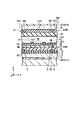
- FIG. 4 is a cross-sectional view showing a configuration example of the liquid crystal display device DSP shown in FIG.
- the illustrated example corresponds to an example in which the FFS (Fringe Field Switching) mode, which is one of the display modes using the lateral electric field, is applied.
- the first substrate SUB1 includes an insulating substrate 10, insulating layers 11 to 16, semiconductor layer SC, signal line S, metal wiring ML, common electrode CE, pixel electrode PE, alignment film AL1, and the like.
- the insulating substrate 10 is a transparent substrate such as a glass substrate or a flexible resin substrate.
- the insulating layer 11 is located on the insulating substrate 10.
- the semiconductor layer SC is located on the insulating layer 11 and is covered with the insulating layer 12.
- the semiconductor layer SC is formed of, for example, polycrystalline silicon, but may be formed of amorphous silicon or an oxide semiconductor.
- the insulating layer 12 is covered with the insulating layer 13.
- the scanning line G shown in FIG. 3 is located between the insulating layers 12 and 13.
- the signal line S is located on the insulating layer 13 and is covered with the insulating layer 14.
- the metal wiring ML is located on the insulating layer 14 and is covered by the insulating layer 15.
- the metal wiring ML includes, for example, metal materials such as aluminum (Al), titanium (Ti), silver (Ag), molybdenum (Mo), tungsten (W), copper (Cu), and chromium (Cr), and these metals. It is formed of an alloy that combines materials.
- the metal wiring ML may have a single-layer structure or a multi-layer structure. Each of the metal wiring MLs extends parallel to the signal line S and is located directly above the signal line S.
- the common electrode CE is located on the insulating layer 15 and is covered with the insulating layer 16.
- the pixel electrode PE is located on the insulating layer 16 and is covered with the alignment film AL1.
- Each of the pixel electrode PEs faces the common electrode CE via the insulating layer 16.
- the common electrode CE and the pixel electrode PE are formed of, for example, a transparent conductive material such as ITO or IZO.
- the pixel electrode PE is a linear electrode
- the common electrode CE is a flat plate-shaped electrode commonly provided over a plurality of pixel PXs.
- the pixel electrode PE may be a flat plate electrode, and a linear common electrode may be provided between the pixel electrode PE and the liquid crystal layer LC.
- the insulating layer 11, the insulating layer 12, and the insulating layers 13 and 16 are inorganic insulating layers formed of an inorganic insulating material such as silicon oxide (SiO), silicon nitride (SiN), and silicon oxynitride (SiON). ..
- the insulating layer 16 is formed of, for example, silicon nitride.
- the insulating layer 11, the insulating layer 12, and the insulating layers 13 and 16 may have a single-layer structure or a multi-layer structure.
- the insulating layers 14 and 15 are organic insulating layers formed of, for example, an organic insulating material such as an acrylic resin.
- the second substrate SUB2 includes an insulating substrate 20, a colored layer CF, a light-shielding layer BM, a transparent layer OC, and an alignment film AL2.
- the insulating substrate 20 is a transparent substrate such as a glass substrate or a flexible resin substrate.
- the colored layer CF, the light-shielding layer BM, and the transparent layer OC are located between the insulating substrate 20 and the liquid crystal layer LC.
- the alignment film AL2 is in contact with the liquid crystal layer LC.
- the alignment films AL1 and AL2 are formed of, for example, a material exhibiting horizontal orientation.
- the transparent layer OC covers the colored layer CF and the light-shielding layer BM.
- the transparent layer OC is, for example, a transparent organic insulating layer.
- the colored layer CF is provided on the second substrate SUB2, but it may be provided on the first substrate SUB1.
- the colored layer CF includes a red layer CFR, a green layer CFG, and a blue layer CFB.
- the green layer CFG faces the pixel electrode PE.
- the red layer CFR and the blue layer CFB also face each other pixel electrode PE (not shown).
- the liquid crystal layer LC is located between the first substrate SUB1 and the second substrate SUB2, and is held between the alignment film AL1 and the alignment film AL2.
- the liquid crystal layer LC includes a liquid crystal molecule LM.
- the liquid crystal layer LC is composed of a positive type (positive dielectric anisotropy) liquid crystal material or a negative type (negative dielectric anisotropy) liquid crystal material.
- the liquid crystal molecules LM are initially oriented in a predetermined direction between the alignment films AL1 and AL2 in an off state in which an electric field is not formed between the pixel electrode PE and the common electrode CE. ing. In such an off state, the illumination light emitted from the illumination device IL toward the display panel PNL is absorbed by the optical elements OD1 and OD2, resulting in dark display. On the other hand, in the on state where an electric field is formed between the pixel electrode PE and the common electrode CE, the liquid crystal molecule LM is oriented in a direction different from the initial orientation direction due to the electric field, and the orientation direction is controlled by the electric field. .. In such an on state, a part of the illumination light from the illumination device IL passes through the optical elements OD1 and OD2 and becomes a bright display.
- FIG. 5 is a plan view showing a configuration example of the touch sensor TS included in the liquid crystal display device DSP shown in FIG.
- the touch sensor TS may be a mutual capacity type touch sensor TS.
- the touch sensor TS includes a plurality of electrodes Rx (Rx1, Rx2 ...) And a plurality of sensor wirings L.
- the plurality of electrodes Rx are located in the display region DA and are arranged in a matrix in the first direction X and the second direction Y.
- the electrode Rx is not provided in the window region WA.
- the electrode Rx2 has a square shape, but the electrode Rx1 arranged around the window region WA has a shape along the window region WA.
- the plurality of sensor wirings L extend along the second direction Y and are lined up in the first direction X in the display area DA. Each of the sensor wirings L is provided at a position overlapping the signal line S described above. Further, each of the sensor wirings L is drawn out to the extension area EA and is electrically connected to the IC chip 1 via the wiring board F1. Each of the sensor wires L is electrically connected to one electrode Rx. In addition, one electrode Rx and a plurality of sensor wirings L may be electrically connected.
- the touch controller TCN applies a touch drive voltage to the sensor wiring L.
- a touch drive voltage is applied to the electrode Rx, and sensing is performed on the electrode Rx.
- the sensor signal corresponding to the sensing result at the electrode Rx is output to the touch controller TCN via the sensor wiring L.
- the electrode Rx functions as a common electrode CE to which a common voltage (Vcom) is applied.
- the common voltage is applied from the voltage supply unit included in the display driver DD, for example, via the sensor wiring L.
- the metal wiring ML shown in FIG. 4 functions as the sensor wiring L.
- FIG. 6 is an enlarged plan view of the window area WA shown in FIG.
- the liquid crystal display device DSP further includes a plurality of transparent conductive layer TCs.
- the transparent conductive layer TC is formed of the same material as the pixel electrode PE shown in FIG.
- the transparent conductive layer TC is provided over the frame region FRA and the window region WA.
- Each of the transparent conductive layer TCs is separated from each other and is connected to different electrodes Rx1 in the frame region FRA via a contact hole CH described later.
- the electrode Rx functions as a sensor electrode in the touch sensing mode, it is preferable that the areas of the electrodes Rx are the same.
- the area of the electrode Rx1 that overlaps the window region WA is smaller than the area of the electrode Rx2 that does not overlap the window region WA.
- the electrode Rx1 and the transparent conductive layer TC function as one sensor electrode.
- the total value of the area of the electrode Rx1 and the area of the transparent conductive layer TC connected to the electrode Rx1 is substantially the same as the area of the electrode Rx2. Therefore, it is possible to suppress a decrease in touch sensing accuracy in the vicinity of the window region WA.
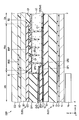
- FIG. 7 is a cross-sectional view of the liquid crystal display device DSP along the line AB shown in FIG.
- the transparent conductive layer TC is located on the insulating layer 16 and is covered with the alignment film AL1.
- the transparent conductive layer TC is connected to the common electrode CE via a contact hole CH penetrating the insulating layer 16.
- there is only one contact hole CH but a plurality of contact hole CHs may be formed as long as the transparent conductive layer TC and the common electrode CE overlap in the frame region FRA.
- the transparent conductive layer TC may be connected to the common electrode CE via a plurality of contact hole CHs.
- the transparent conductive layer TC is in contact with the insulating layer 16 and the alignment film AL1 in the frame region FRA, and is in contact with the insulating layer 16 and the spacer SP2 in the window region WA.
- the light-shielding layer BMP is provided on the lower surface of the insulating substrate 20.
- the outer surface BO of the light-shielding layer BMP is covered with the colored layer CF, and the inner surface BI is located below the light-shielding layer BMC.
- Each of the plurality of colored layer CFs is located between the light-shielding layer BMP and the transparent layer OC in the frame region FRA.
- the liquid crystal display device DSP further includes a plurality of spacers SP (SP1, SP2, ...) Located between the first substrate SUB1 and the second substrate SUB2.
- the spacer SP is formed of, for example, a member that transmits light.
- the spacers SP1 and SP3 are provided on the second substrate SUB2, and the spacer SP2 is provided on the first substrate SUB1.
- One spacer SP1 is located in the window area WA.
- the spacer SP1 is provided on the lower surface of the transparent layer OC and is covered with the alignment film AL2.
- the spacer SP1 has an outer peripheral surface OF1 located below the light-shielding layer BMC.
- One spacer SP2 is located in the window area WA and the frame area FRA.
- the spacer SP2 is in contact with the transparent conductive layer TC and is covered with the alignment film AL1.
- the spacer SP2 has an outer peripheral surface OF2 located below the light-shielding layer BMC.
- the spacer SP1 and the spacer SP2 face each other.
- Spacers SP1 and SP2 are provided substantially over the entire window area WA.
- the inner surface BI of the light-shielding layer BMP is located between the outer peripheral surface OF1 and the outer peripheral surface OF2.
- the liquid crystal layer LC extends between the spacer SP1 and the spacer SP2.
- the plurality of spacers SP3 are located in the frame region FRA. Each of the spacers SP3 faces the colored layer CF and is located between the transparent layer OC and the first substrate SUB1.
- the plurality of spacers SP3 are for maintaining a cell gap between the first substrate SUB1 and the second substrate SUB2 in the frame region FRA.
- the plurality of spacers SP3 include a main spacer that is in contact with the first substrate SUB1 and a subspacer that is not in contact with the first substrate SUB1 in a steady state in which no external stress is applied to the display panel PNL.
- the window region WA of the display panel PNL is not provided with a member such as a metal wiring ML or a colored layer CF that blocks light, but is provided with only a member that transmits light such as an insulating layer, a spacer SP, or a transparent layer OC. .. Further, the liquid crystal molecules of the liquid crystal layer LC located in the window region WA transmit light, for example, in a state where an electric field is not applied. As a result, the light receiving element PA located in the window region WA can receive light via the transparent substrate CG and the display panel PNL, respectively.
- the window area WA overlaps with the camera as the light receiving element PA, and the window area WA is required to have transparency that does not interfere with the image pickup of the camera.
- the window region WA is not provided with the switching element SW constituting the thin film transistor, the scanning line G, and the signal line S as members for blocking light, and the window region WA is displayed. It may be rephrased as a highly transparent region WA or a highly transparent region WA having a higher light transmittance (high transparency) than the region DA.
- the high light transmittance region WA may be a region having a higher light transmittance than the display region DA, and a light shielding member such as a metal wiring ML is provided as long as the function of the light receiving element PA including the camera is not impaired. May be good.
- the optical elements OD1 and OD2 shown in FIG. 1 do not have to form through holes in both of them in the high translucency region WA, and form through holes in only one of the optical element OD1 and the optical element OD2. There may be. Even in this case, the high light transmittance WA has a higher light transmittance than the display area DA. Needless to say, as shown in FIG. 1, it is more appropriate that the metal wiring and the polarizing plate composed of two optical elements, which can hinder light transmission, are not in the high light transmission region WA.
- the cell gap between the first substrate SUB1 and the second substrate SUB2 is maintained in the window region WA. can do. Therefore, when an external stress is applied to the window region WA of the display panel PNL, it is possible to prevent uneven cell gaps from occurring between the window region WA and other regions (frame region FRA and display region DA). .. Further, when a plurality of spacers SP1 and a plurality of spacers SP2 are provided in the window area WA, the light transmitted through the window area WA may be reflected by the plurality of spacers SP1 and the plurality of spacers SP2 and visually recognized, or in the window area WA.
- the light receiving element PA it is not necessary to provide a through hole in the window area WA as compared with the case where the window area WA of the display panel PNL is provided with a through hole, and to provide the through hole. Since it is not necessary to arrange a seal for sealing the liquid crystal layer LC around the through hole, the manufacturing process can be simplified and the frame region FRA can be narrowed.
- a transparent conductive layer TC is provided between the alignment film AL1 and the inorganic insulating layer 16. Since the adhesive strength between the alignment film AL1 and the transparent conductive layer TC is stronger than the adhesive strength between the alignment film AL1 and the inorganic insulating layer 16, peeling of the alignment film AL1 can be suppressed in the frame region FRA.
- the insulating layer 16 corresponds to the inorganic insulating layer
- the insulating layer 14 corresponds to the first organic insulating layer
- the insulating layer 15 corresponds to the second organic insulating layer
- the spacer SP1 corresponds to the first spacer
- the spacer SP2 corresponds to the second spacer
- the spacer SP3 corresponds to the third spacer.
- FIG. 8 is a plan view of the liquid crystal display device DSP, and is a diagram for explaining the positional relationship of each spacer SP. As shown in FIG. 8, the plurality of spacers SP3 are scattered in the frame region FRA, and the plurality of spacers SP4 are scattered in the display region DA.
- the plurality of spacers SP4 are located in the display area DA.
- the spacer SP4 is provided, for example, at a position where the scanning line G and the signal line S shown in FIG. 3 overlap.
- Each of the spacers SP4 is arranged with an interval DX4 in the first direction X and an interval DY4 in the second direction Y.
- Each of the spacers SP3 is arranged with an interval DX3 in the first direction X and an interval DY3 in the second direction Y.
- the interval DX3 and the interval DX4 are substantially equivalent, and the interval DY3 and the interval DY4 are substantially equivalent.
- the colored layer CFs are scattered in the frame region FRA and are circular in a plan view.
- FIG. 9 is a cross-sectional view showing a modified example of the liquid crystal display device DSP shown in FIG. 7. As shown in FIG. 9, this modification is different from the configuration example shown in FIG. 7 in that the spacer SP2 is not arranged.
- the alignment film AL1 is in contact with the transparent conductive layer TC in the window region WA and the frame region FRA.
- the spacer SP1 is provided on the second substrate SUB2, but the spacer SP1 may be provided on the first substrate SUB1.
- the same effect as described above can be obtained.
- the transparent conductive layer TC is in contact with the alignment film AL1. As a result, peeling of the alignment film AL1 can be suppressed in the window region WA.
Landscapes
- Physics & Mathematics (AREA)
- Nonlinear Science (AREA)
- General Physics & Mathematics (AREA)
- Mathematical Physics (AREA)
- Chemical & Material Sciences (AREA)
- Crystallography & Structural Chemistry (AREA)
- Optics & Photonics (AREA)
- Liquid Crystal (AREA)
- Engineering & Computer Science (AREA)
- Theoretical Computer Science (AREA)
- Devices For Indicating Variable Information By Combining Individual Elements (AREA)
Abstract
製品の歩留まりの改善が可能な液晶表示装置を提供する。 液晶表示装置は、第1基板と、第2基板と、前記第1基板と前記第2基板とが対向する対向領域と、前記第1基板と前記第2基板との間に位置する液晶層及び第1スペーサと、を備える。前記対向領域は、画像を表示する第1領域と、平面視で前記第1領域の内側に位置する第2領域と、前記第1領域と前記第2領域との間に位置し前記第2領域を囲む額縁状の額縁領域と、を含む。前記第2基板は、平面視で前記額縁領域に形成された遮光層を備える。前記第2領域は、前記第1領域に比べ透明度の高い領域である。前記液晶層は、前記第2領域、前記額縁領域及び前記第1領域に位置している。前記第1スペーサは、前記第2領域に位置し、前記第1基板もしくは前記第2基板に設けられている。
Description
本発明の実施形態は、液晶表示装置に関する。
近年、種々の形状の表示装置が提案されている。一例では、映像表示部と透明表示部との間に遮光部を有する液晶表示装置が開示されている。その他の例では、表示部と、カメラに重なる透明部と、を有する液晶表示装置が開示されている。
本実施形態の目的は、製品の歩留まりの改善が可能な液晶表示装置を提供することにある。
一実施形態に係る液晶表示装置は、
第1基板と、第2基板と、前記第1基板と前記第2基板とが対向する対向領域と、前記第1基板と前記第2基板との間に位置する液晶層及び第1スペーサと、を備え、前記対向領域は、画像を表示する第1領域と、平面視で前記第1領域の内側に位置する第2領域と、前記第1領域と前記第2領域との間に位置し前記第2領域を囲む額縁状の額縁領域と、を含み、前記第2基板は、平面視で前記額縁領域に形成された遮光層を備え、前記第2領域は、前記第1領域に比べ透明度の高い領域であり、前記液晶層は、前記第2領域、前記額縁領域及び前記第1領域に位置し、前記第1スペーサは、前記第2領域に位置し、前記第1基板もしくは前記第2基板に設けられている。
第1基板と、第2基板と、前記第1基板と前記第2基板とが対向する対向領域と、前記第1基板と前記第2基板との間に位置する液晶層及び第1スペーサと、を備え、前記対向領域は、画像を表示する第1領域と、平面視で前記第1領域の内側に位置する第2領域と、前記第1領域と前記第2領域との間に位置し前記第2領域を囲む額縁状の額縁領域と、を含み、前記第2基板は、平面視で前記額縁領域に形成された遮光層を備え、前記第2領域は、前記第1領域に比べ透明度の高い領域であり、前記液晶層は、前記第2領域、前記額縁領域及び前記第1領域に位置し、前記第1スペーサは、前記第2領域に位置し、前記第1基板もしくは前記第2基板に設けられている。
以下、本実施形態について、図面を参照しながら説明する。なお、開示はあくまで一例に過ぎず、当業者において、発明の主旨を保っての適宜変更について容易に想到し得るものについては、当然に本発明の範囲に含有されるものである。また、図面は、説明をより明確にするため、実際の態様に比べて、各部の幅、厚さ、形状等について模式的に表される場合があるが、あくまで一例であって、本発明の解釈を限定するものではない。また、本明細書と各図において、既出の図に関して前述したものと同一又は類似した機能を発揮する構成要素には同一の参照符号を付し、重複する詳細な説明を適宜省略することがある。
図1は、一実施形態の液晶表示装置DSPの断面図である。一例では、第1方向X、第2方向Y、及び、第3方向Zは、互いに直交しているが、90度以外の角度で交差していてもよい。本明細書において、第3方向Zを示す矢印の先端側の位置を上と称し、矢印の先端とは逆側の位置を下と称する。また、上から下に向かって、第1方向X及び第2方向Yで規定されるX-Y平面に向かって見ることを平面視という。
図1に示すように、液晶表示装置DSPは、透明基板CGと、表示パネルPNLと、照明装置ILと、電子部品PAと、を備えている。透明基板CG、表示パネルPNL、及び電子部品PAは、この順に第3方向Zに沿って並んでいる。
図1に示すように、液晶表示装置DSPは、透明基板CGと、表示パネルPNLと、照明装置ILと、電子部品PAと、を備えている。透明基板CG、表示パネルPNL、及び電子部品PAは、この順に第3方向Zに沿って並んでいる。
表示パネルPNLは、第1基板SUB1と、第2基板SUB2と、光学素子OD1と、光学素子OD2と、を備えている。
第2基板SUB2は、遮光層BMPを備えている。遮光層BMPは、第1基板SUB1と第2基板SUB2との間に位置している。偏光板PL1を含む光学素子OD1は、第1基板SUB1に接着されている。偏光板PL2を含む光学素子OD2は、第2基板SUB2に接着されている。光学素子OD1及びOD2は、それぞれ第3方向Zにおいて電子部品PAに重なる位置に貫通孔を有している。なお、光学素子OD1及びOD2は、必要に応じて位相差板、拡散層、反射防止層などを備えていてもよい。
第2基板SUB2は、遮光層BMPを備えている。遮光層BMPは、第1基板SUB1と第2基板SUB2との間に位置している。偏光板PL1を含む光学素子OD1は、第1基板SUB1に接着されている。偏光板PL2を含む光学素子OD2は、第2基板SUB2に接着されている。光学素子OD1及びOD2は、それぞれ第3方向Zにおいて電子部品PAに重なる位置に貫通孔を有している。なお、光学素子OD1及びOD2は、必要に応じて位相差板、拡散層、反射防止層などを備えていてもよい。
透明基板CGは、透明接着層ADによって表示パネルPNLに接着されている。透明基板CGは、遮光層BMCを備えている。図示した例では、遮光層BMCは、透明基板CGの下面に設けられ、第3方向Zにおいて遮光層BMPに重なっている。透明基板CGは、ガラス基板や可撓性の樹脂基板などである。
照明装置ILは、表示パネルPNLを照明するものである。図示した例では、照明装置ILは、第3方向Zにおいて電子部品PAに重なる貫通孔THを有している。
電子部品PAは本実施例においては受光素子PAであり、受光素子PAは一例としてカメラである。なお、受光素子PAは、一例として、可視光を検出するもの、赤外線を検出するもの、検出対象物の近接をセンシングする近接センサ、検出対象物から反射された赤外線を検出する検出素子などや、それぞれを組み合わせたものでもよい。受光素子PAは、照明装置ILの貫通孔THに挿入されている。受光素子PAは、第3方向Zにおいて、透明基板CG、透明接着層AD又は表示パネルPNLを介して受光する。
図2は、図1に示した液晶表示装置DSPの平面図である。
図2に示すように、液晶表示装置DSPは、さらに、配線基板F1とICチップ1とを備えている。
図2に示すように、液晶表示装置DSPは、さらに、配線基板F1とICチップ1とを備えている。
表示パネルPNLは、第2方向Yに沿って並んだ対向領域FA及び延出領域EAを有している。対向領域FAは、第1基板SUB1と第2基板SUB2とが対向し重なり合う領域であり、表示パネルPNLの2枚部分である。延出領域EAは、第1基板SUB1が第2基板SUB2から露出する表示パネルPNLの1枚部分ということもできる。
対向領域FAは、画像を表示する表示領域DAと、表示領域DAを囲む額縁状の非表示領域NDAと、窓領域WAと、額縁領域FRAと、を含んでいる。窓領域WAは、平面視で表示領域DAの内側に位置している。図示した例では、窓領域WAは真円であるが、楕円等の他の円形や円形以外の多角形であってもよい。額縁領域FRAは、表示領域DAと窓領域WAとの間に位置し、窓領域WAを囲む額縁状の領域である。また、表示領域DAを第1領域、窓領域WAを第2領域と言い換えてもよい。
表示領域DAには、第1方向(行方向)X及び第2方向(列方向)Yにマトリクス状(行列状)に配置された複数の画素PXが位置している。なお、画素PXは、窓領域WA及び額縁領域FRAには設けられていない。ここでの画素PXとは、画素信号に応じて個別に制御することができる最小単位を示し、副画素と称する場合がある。画素PXは、例えば、赤色を呈する赤画素、緑色を呈する緑画素、青色を呈する青画素、または、白色を呈する白画素のいずれかである。
受光素子PAは、平面視で窓領域WAの内側に位置している。図1に示した貫通孔THは、窓領域WAに重なっている。遮光層BMPは、額縁領域FRA全域に設けられている。遮光層BMPは、内面BIと外面BOとを有している。内面BIは窓領域WAと額縁領域FRAとの境界に相当し、外面BOは額縁領域FRAと表示領域DAとの境界に相当する。
受光素子PAは、平面視で窓領域WAの内側に位置している。図1に示した貫通孔THは、窓領域WAに重なっている。遮光層BMPは、額縁領域FRA全域に設けられている。遮光層BMPは、内面BIと外面BOとを有している。内面BIは窓領域WAと額縁領域FRAとの境界に相当し、外面BOは額縁領域FRAと表示領域DAとの境界に相当する。
ICチップ1及び配線基板F1は、表示パネルPNLからの信号を読み出す場合もあるが、主として表示パネルPNLに信号を供給する信号源として機能する。ICチップ1は、配線基板F1に実装され、配線基板F1に電気的に接続されている。なお、ICチップ1は、延出領域EAに実装され、延出領域EAに電気的に接続されていてもよい。ICチップ1は、画像を表示する画像表示モードにおいて画像表示に必要な信号を出力するディスプレイドライバDDを内蔵している。また、図示した例では、ICチップ1は、液晶表示装置DSPへの物体の接近又は接触を検出するタッチセンシングモードを制御するタッチコントローラTCNを内蔵している。図中において、ディスプレイドライバDD及びタッチコントローラTCNは点線で示している。配線基板F1は、折り曲げ可能なフレキシブルプリント基板である。
表示パネルPNLは、さらに液晶層LCと、シールSEと、を備えている。シールSEは非表示領域NDAに位置し、第1基板SUB1と第2基板SUB2とを接合している。液晶層LCは、第1基板SUB1と第2基板SUB2との間に保持され、シールSEによって封止されている。液晶層LCは、窓領域WA、額縁領域FRA及び表示領域DAのそれぞれにわたって設けられている。図2において、液晶層LC及びシールSEは、異なる斜線で示している。
また、表示パネルPNLの詳細な構成について、ここでは説明を省略するが、表示パネルPNLは、基板主面に沿った横電界を利用する表示モード、基板主面の法線に沿った縦電界を利用する表示モード、基板主面に対して斜め方向に傾斜した傾斜電界を利用する表示モード、さらには、上記の横電界、縦電界、及び、傾斜電界を適宜組み合わせて利用する表示モードに対応したいずれの構成を備えていてもよい。ここでの基板主面とは、第1方向X及び第2方向Yで規定されるX-Y平面と平行な面である。
図3は、図2に示した画素の基本構造及び等価回路を示す図である。
図3に示すように、複数本の走査線Gは走査線駆動回路GDに接続され、複数本の信号線Sは信号線駆動回路SDに接続されている。走査線G及び信号線Sは、それぞれ、アルミニウム(Al)、チタン(Ti)、銀(Ag)、モリブデン(Mo)、タングステン(W)、銅(Cu)、クロム(Cr)などの金属材料や、これらの金属材料を組み合わせた合金などによって形成されている。走査線G及び信号線Sは、それぞれ、単層構造であってもよいし、多層構造であってもよい。なお、走査線G及び信号線Sは、必ずしも直線的に延出していなくてもよく、それらの一部が屈曲していてもよい。
図3に示すように、複数本の走査線Gは走査線駆動回路GDに接続され、複数本の信号線Sは信号線駆動回路SDに接続されている。走査線G及び信号線Sは、それぞれ、アルミニウム(Al)、チタン(Ti)、銀(Ag)、モリブデン(Mo)、タングステン(W)、銅(Cu)、クロム(Cr)などの金属材料や、これらの金属材料を組み合わせた合金などによって形成されている。走査線G及び信号線Sは、それぞれ、単層構造であってもよいし、多層構造であってもよい。なお、走査線G及び信号線Sは、必ずしも直線的に延出していなくてもよく、それらの一部が屈曲していてもよい。
共通電極CEは、複数の画素PXにわたって配置されている。共通電極CEは、電圧供給部CD及び図2に示したタッチコントローラTCNに接続されている。画像表示モードにおいては、電圧供給部CDは、共通電極CEにコモン電圧(Vcom)を供給する。タッチセンシングモードにおいては、タッチコントローラTCNは、コモン電圧とは異なるタッチ駆動電圧を共通電極CEに供給する。
各画素PXは、スイッチング素子SW、画素電極PE、共通電極CE、液晶層LC等を備えている。スイッチング素子SWは、例えば薄膜トランジスタ(TFT)によって構成され、走査線G及び信号線Sと電気的に接続されている。走査線Gは、第1方向Xに並んだ画素PXの各々におけるスイッチング素子SWと電気的に接続されている。信号線Sは、第2方向Yに並んだ画素PXの各々におけるスイッチング素子SWと電気的に接続されている。走査線Gには、スイッチング素子SWを制御するための制御信号が供給される。信号線Sには、制御信号とは異なる信号として、映像信号が供給される。画素電極PEは、スイッチング素子SWと電気的に接続されている。液晶層LCは、画素電極PEと共通電極CEとの間に生じる電界によって駆動されている。容量CSは、例えば、共通電極CEと同電位の電極、及び、画素電極PEと同電位の電極の間に形成される。
図4は、図1に示した液晶表示装置DSPの一構成例を示す断面図である。図示した例は、横電界を利用する表示モードの一つであるFFS(Fringe Field Switching)モードが適用された例に相当する。
図4に示すように、第1基板SUB1は、絶縁基板10、絶縁層11乃至16、半導体層SC、信号線S、金属配線ML、共通電極CE、画素電極PE、配向膜AL1などを備えている。絶縁基板10は、ガラス基板や可撓性の樹脂基板などの透明基板である。絶縁層11は、絶縁基板10の上に位置している。半導体層SCは、絶縁層11の上に位置し、絶縁層12によって覆われている。半導体層SCは、例えば、多結晶シリコンによって形成されているが、アモルファスシリコンや酸化物半導体によって形成されていてもよい。絶縁層12は、絶縁層13によって覆われている。図3に示した走査線Gは、絶縁層12及び13の間に位置している。信号線Sは、絶縁層13の上に位置し、絶縁層14によって覆われている。金属配線MLは、絶縁層14の上に位置し、絶縁層15によって覆われている。金属配線MLは、例えば、アルミニウム(Al)、チタン(Ti)、銀(Ag)、モリブデン(Mo)、タングステン(W)、銅(Cu)、クロム(Cr)などの金属材料や、これらの金属材料を組み合わせた合金などによって形成されている。金属配線MLは、単層構造であってもよいし、多層構造であってもよい。金属配線MLは、それぞれ信号線Sと平行に延出し、信号線Sの直上に位置している。
図4に示すように、第1基板SUB1は、絶縁基板10、絶縁層11乃至16、半導体層SC、信号線S、金属配線ML、共通電極CE、画素電極PE、配向膜AL1などを備えている。絶縁基板10は、ガラス基板や可撓性の樹脂基板などの透明基板である。絶縁層11は、絶縁基板10の上に位置している。半導体層SCは、絶縁層11の上に位置し、絶縁層12によって覆われている。半導体層SCは、例えば、多結晶シリコンによって形成されているが、アモルファスシリコンや酸化物半導体によって形成されていてもよい。絶縁層12は、絶縁層13によって覆われている。図3に示した走査線Gは、絶縁層12及び13の間に位置している。信号線Sは、絶縁層13の上に位置し、絶縁層14によって覆われている。金属配線MLは、絶縁層14の上に位置し、絶縁層15によって覆われている。金属配線MLは、例えば、アルミニウム(Al)、チタン(Ti)、銀(Ag)、モリブデン(Mo)、タングステン(W)、銅(Cu)、クロム(Cr)などの金属材料や、これらの金属材料を組み合わせた合金などによって形成されている。金属配線MLは、単層構造であってもよいし、多層構造であってもよい。金属配線MLは、それぞれ信号線Sと平行に延出し、信号線Sの直上に位置している。
共通電極CEは、絶縁層15の上に位置し、絶縁層16によって覆われている。画素電極PEは、絶縁層16の上に位置し、配向膜AL1によって覆われている。画素電極PEの各々は、絶縁層16を介して、共通電極CEと対向している。共通電極CE及び画素電極PEは、例えば、ITOやIZOなどの透明な導電材料によって形成されている。画素電極PEは、線状電極であり、共通電極CEは、複数の画素PXにわたって共通に設けられた平板状の電極である。なお、画素電極PEを平板状の電極とし、画素電極PEと液晶層LCとの間に線状の共通電極を設ける構造であってもよい。
絶縁層11、絶縁層12、絶縁層13及び16は、シリコン酸化物(SiO)、シリコン窒化物(SiN)、シリコン酸窒化物(SiON)などの無機絶縁材料によって形成された無機絶縁層である。絶縁層16は、例えば、シリコン窒化物によって形成されている。絶縁層11、絶縁層12、絶縁層13及び16は、単層構造であってもよいし、多層構造であってもよい。絶縁層14及び15は、例えば、アクリル樹脂などの有機絶縁材料によって形成された有機絶縁層である。
第2基板SUB2は、絶縁基板20と、着色層CFと、遮光層BMと、透明層OCと、配向膜AL2とを備えている。絶縁基板20は、ガラス基板や可撓性の樹脂基板などの透明基板である。着色層CF、遮光層BM、及び、透明層OCは、絶縁基板20と液晶層LCとの間に位置している。配向膜AL2は、液晶層LCに接している。配向膜AL1及びAL2は、例えば、水平配向性を呈する材料によって形成されている。透明層OCは、着色層CF及び遮光層BMを覆っている。透明層OCは、例えば、透明な有機絶縁層である。なお、図示した例では、着色層CFは、第2基板SUB2に設けられたが、第1基板SUB1に設けられてもよい。着色層CFは、赤色層CFR、緑色層CFG、及び、青色層CFBを含んでいる。緑色層CFGは、画素電極PEと対向している。赤色層CFR及び青色層CFBも、それぞれ図示しない他の画素電極PEと対向している。
液晶層LCは、第1基板SUB1及び第2基板SUB2の間に位置し、配向膜AL1と配向膜AL2との間に保持されている。液晶層LCは、液晶分子LMを備えている。液晶層LCは、ポジ型(誘電率異方性が正)の液晶材料、あるいは、ネガ型(誘電率異方性が負)の液晶材料によって構成されている。
このような表示パネルPNLにおいては、画素電極PEと共通電極CEとの間に電界が形成されていないオフ状態において、液晶分子LMは、配向膜AL1及びAL2の間で所定の方向に初期配向している。このようなオフ状態では、照明装置ILから表示パネルPNLに向けて照射された照明光は、光学素子OD1及びOD2によって吸収され、暗表示となる。一方、画素電極PEと共通電極CEとの間に電界が形成されたオン状態においては、液晶分子LMは、電界により初期配向方向とは異なる方向に配向し、その配向方向は電界によって制御される。このようなオン状態では、照明装置ILからの照明光の一部は、光学素子OD1及びOD2を透過し、明表示となる。
図5は、図2に示した液晶表示装置DSPが有するタッチセンサTSの一構成例を示す平面図である。ここでは、自己容量方式のタッチセンサTSについて説明するが、タッチセンサTSは相互容量方式のタッチセンサTSであってもよい。
図5に示すように、タッチセンサTSは、複数の電極Rx(Rx1、Rx2…)と、複数のセンサ配線Lと、を備えている。複数の電極Rxは、表示領域DAに位置し、第1方向X及び第2方向Yにマトリクス状に配置されている。なお、電極Rxは窓領域WAには設けられていない。図示した例では、電極Rx2は正方形状であるが、窓領域WA周辺に配置された電極Rx1は窓領域WAに沿った形状を有している。複数のセンサ配線Lは、表示領域DAにおいて、それぞれ第2方向Yに沿って延出し、第1方向Xに並んでいる。センサ配線Lの各々は、上記した信号線Sと重なる位置に設けられている。また、センサ配線Lの各々は、延出領域EAに引き出され、配線基板F1を介してICチップ1に電気的に接続されている。センサ配線Lの各々は、1つの電極Rxと電気的に接続されている。なお、1つの電極Rxと複数のセンサ配線Lとが電気的に接続されてもよい。
図5に示すように、タッチセンサTSは、複数の電極Rx(Rx1、Rx2…)と、複数のセンサ配線Lと、を備えている。複数の電極Rxは、表示領域DAに位置し、第1方向X及び第2方向Yにマトリクス状に配置されている。なお、電極Rxは窓領域WAには設けられていない。図示した例では、電極Rx2は正方形状であるが、窓領域WA周辺に配置された電極Rx1は窓領域WAに沿った形状を有している。複数のセンサ配線Lは、表示領域DAにおいて、それぞれ第2方向Yに沿って延出し、第1方向Xに並んでいる。センサ配線Lの各々は、上記した信号線Sと重なる位置に設けられている。また、センサ配線Lの各々は、延出領域EAに引き出され、配線基板F1を介してICチップ1に電気的に接続されている。センサ配線Lの各々は、1つの電極Rxと電気的に接続されている。なお、1つの電極Rxと複数のセンサ配線Lとが電気的に接続されてもよい。
タッチセンシングモードにおいては、タッチコントローラTCNは、センサ配線Lにタッチ駆動電圧を印加する。これにより、電極Rxにはタッチ駆動電圧が印加され、電極Rxでのセンシングが行われる。電極Rxでのセンシング結果に対応したセンサ信号は、センサ配線Lを介してタッチコントローラTCNに出力される。
なお、表示モードにおいては、電極Rxは、コモン電圧(Vcom)が印加された共通電極CEとして機能する。コモン電圧は、例えばディスプレイドライバDDに含まれる電圧供給部からセンサ配線Lを介して印加される。図4に示した金属配線MLはセンサ配線Lとして機能する。
図6は、図5に示した窓領域WAを拡大した平面図である。
図6に示すように、液晶表示装置DSPは、さらに、複数の透明導電層TCを備えている。透明導電層TCは、図4に示した画素電極PEと同一材料によって形成されている。透明導電層TCは、額縁領域FRA及び窓領域WAにわたって設けられている。透明導電層TCの各々は、互いに離れていて、それぞれ額縁領域FRAにおいて異なる電極Rx1に後述するコンタクトホールCHを介して接続されている。
タッチセンシングモードにおいて電極Rxをセンサ電極として機能させる場合、電極Rxの各々の面積が同等であることが好ましい。窓領域WAに重なる電極Rx1の面積は、窓領域WAに重ならない電極Rx2の面積より小さい。しかし、電極Rx1と透明導電層TCとが電気的に接続することにより、電極Rx1と透明導電層TCとは一つのセンサ電極として機能する。電極Rx1の面積及び電極Rx1に接続される透明導電層TCの面積の合計値は、電極Rx2の面積と実質的に同等となる。このため、窓領域WAの近傍におけるタッチセンシング精度の低下を抑制することができる。
図6に示すように、液晶表示装置DSPは、さらに、複数の透明導電層TCを備えている。透明導電層TCは、図4に示した画素電極PEと同一材料によって形成されている。透明導電層TCは、額縁領域FRA及び窓領域WAにわたって設けられている。透明導電層TCの各々は、互いに離れていて、それぞれ額縁領域FRAにおいて異なる電極Rx1に後述するコンタクトホールCHを介して接続されている。
タッチセンシングモードにおいて電極Rxをセンサ電極として機能させる場合、電極Rxの各々の面積が同等であることが好ましい。窓領域WAに重なる電極Rx1の面積は、窓領域WAに重ならない電極Rx2の面積より小さい。しかし、電極Rx1と透明導電層TCとが電気的に接続することにより、電極Rx1と透明導電層TCとは一つのセンサ電極として機能する。電極Rx1の面積及び電極Rx1に接続される透明導電層TCの面積の合計値は、電極Rx2の面積と実質的に同等となる。このため、窓領域WAの近傍におけるタッチセンシング精度の低下を抑制することができる。
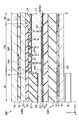
図7は、図6に示したA-B線に沿った液晶表示装置DSPの断面図である。
図7に示すように、透明導電層TCは、絶縁層16の上に位置し、配向膜AL1に覆われている。透明導電層TCは、絶縁層16を貫通するコンタクトホールCHを介して共通電極CEに接続している。図示した例では、コンタクトホールCHは1つであるが、額縁領域FRAにおいて透明導電層TCと共通電極CEとが重なる領域であれば複数のコンタクトホールCHを形成してもよい。透明導電層TCは複数のコンタクトホールCHを介して共通電極CEに接続してもよい。図示した例では、透明導電層TCは、額縁領域FRAにおいて絶縁層16及び配向膜AL1に接し、窓領域WAにおいては絶縁層16及びスペーサSP2に接している。
図7に示すように、透明導電層TCは、絶縁層16の上に位置し、配向膜AL1に覆われている。透明導電層TCは、絶縁層16を貫通するコンタクトホールCHを介して共通電極CEに接続している。図示した例では、コンタクトホールCHは1つであるが、額縁領域FRAにおいて透明導電層TCと共通電極CEとが重なる領域であれば複数のコンタクトホールCHを形成してもよい。透明導電層TCは複数のコンタクトホールCHを介して共通電極CEに接続してもよい。図示した例では、透明導電層TCは、額縁領域FRAにおいて絶縁層16及び配向膜AL1に接し、窓領域WAにおいては絶縁層16及びスペーサSP2に接している。
遮光層BMPは絶縁基板20の下面に設けられている。図示した例では、遮光層BMPの外面BOは着色層CFに覆われ、内面BIは遮光層BMCの下方に位置している。複数の着色層CFは、それぞれ額縁領域FRAにおいて遮光層BMPと透明層OCとの間に位置している。
液晶表示装置DSPは、さらに、第1基板SUB1と第2基板SUB2との間に位置する複数のスペーサSP(SP1、SP2、…)を備えている。スペーサSPは、例えば光を透過する部材で形成されている。スペーサSP1及びSP3は第2基板SUB2に設けられ、スペーサSP2は第1基板SUB1に設けられている。
1つのスペーサSP1は、窓領域WAに位置している。スペーサSP1は、透明層OCの下面に設けられ、配向膜AL2に覆われている。スペーサSP1は、遮光層BMCの下方に位置する外周面OF1を有している。
1つのスペーサSP2は、窓領域WA及び額縁領域FRAに位置している。スペーサSP2は、透明導電層TCに接し、配向膜AL1に覆われている。スペーサSP2は、遮光層BMCの下方に位置する外周面OF2を有している。
スペーサSP1とスペーサSP2とは対向している。スペーサSP1及びSP2は、実質的に窓領域WAの全域に設けられている。遮光層BMPの内面BIは、外周面OF1と外周面OF2との間に位置している。液晶層LCは、スペーサSP1とスペーサSP2との間に延出している。
複数のスペーサSP3は、額縁領域FRAに位置している。スペーサSP3の各々は、着色層CFに対向し、透明層OCと第1基板SUB1との間に位置している。複数のスペーサSP3は額縁領域FRAにおいて第1基板SUB1と第2基板SUB2とのセルギャップを維持するためのものである。複数のスペーサSP3は、第1基板SUB1に接しているメインスペーサと、表示パネルPNLに対して外部応力が加わっていない定常状態で第1基板SUB1に接触していないサブスペーサが含まれている。
1つのスペーサSP1は、窓領域WAに位置している。スペーサSP1は、透明層OCの下面に設けられ、配向膜AL2に覆われている。スペーサSP1は、遮光層BMCの下方に位置する外周面OF1を有している。
1つのスペーサSP2は、窓領域WA及び額縁領域FRAに位置している。スペーサSP2は、透明導電層TCに接し、配向膜AL1に覆われている。スペーサSP2は、遮光層BMCの下方に位置する外周面OF2を有している。
スペーサSP1とスペーサSP2とは対向している。スペーサSP1及びSP2は、実質的に窓領域WAの全域に設けられている。遮光層BMPの内面BIは、外周面OF1と外周面OF2との間に位置している。液晶層LCは、スペーサSP1とスペーサSP2との間に延出している。
複数のスペーサSP3は、額縁領域FRAに位置している。スペーサSP3の各々は、着色層CFに対向し、透明層OCと第1基板SUB1との間に位置している。複数のスペーサSP3は額縁領域FRAにおいて第1基板SUB1と第2基板SUB2とのセルギャップを維持するためのものである。複数のスペーサSP3は、第1基板SUB1に接しているメインスペーサと、表示パネルPNLに対して外部応力が加わっていない定常状態で第1基板SUB1に接触していないサブスペーサが含まれている。
表示パネルPNLの窓領域WAには、金属配線MLや着色層CFなどの光を遮光する部材が設けられず、絶縁層やスペーサSPや透明層OCなどの光を透過する部材のみ設けられている。また、窓領域WAに位置する液晶層LCの液晶分子は、例えば電界が印加されない状態で光を透過する。これにより、窓領域WAに位置する受光素子PAは、透明基板CG及び表示パネルPNLのそれぞれを介して受光することができる。
上述のように、窓領域WAは受光素子PAとしてのカメラと重なることになり、窓領域WAにはカメラの撮像を阻害しない透明性が求められる。窓領域WAには金属配線MLや着色層CF以外にも、薄膜トランジスタを構成するスイッチング素子SWや、走査線G及び信号線Sも光を遮光する部材として設けられておらず、窓領域WAは表示領域DAに比べ高い光透過率(高い透明性)を有する高透光領域WAもしくは高透明領域WAと言い換えてもよい。
高透光領域WAは表示領域DAに比べ高い光透過率を有する領域であればよく、カメラを含む受光素子PAの機能を阻害しない範囲であれば金属配線ML等の遮光部材が設けられていてもよい。さらに図1に示す光学素子OD1及びOD2も高透光領域WAにおいて両方に貫通孔を形成するものでなくともよく、光学素子OD1もしくは光学素子OD2のどちらか一方のみに貫通孔を形成するものであってもよい。この場合であっても高透光領域WAは表示領域DAに比べ高い光透過率を有することにはなる。当然、図1に示すように光透過の阻害要因となりえる金属の配線や2枚の光学素子からなる偏光板などは高透光領域WAにない方が、より適切であることは言うまでもない。
本実施形態によれば、1つのスペーサSP1及び1つのスペーサSP2は実質的に窓領域WA全域に設けられているため、窓領域WAにおいて第1基板SUB1と第2基板SUB2とのセルギャップを維持することができる。このため、表示パネルPNLの窓領域WAに外部応力が加わった際に、窓領域WAと他の領域(額縁領域FRA及び表示領域DA)とでセルギャップのムラが生じることを抑制することができる。さらに、複数のスペーサSP1及び複数のスペーサSP2が窓領域WAに設けられた場合、窓領域WAを透過する光が複数のスペーサSP1及び複数のスペーサSP2で反射され視認されるおそれや窓領域WAにおける光の透過率の低下するおそれがある。本実施形態では、1つのスペーサSP1及び1つのスペーサSP2のみ窓領域WAに設けられているため、上記の不具合を抑制することができ、液晶表示装置DSPの製品の歩留まりの改善が可能である。
また、受光素子PAが光を受光するために、表示パネルPNLの窓領域WAに貫通孔を設ける場合と比較して、窓領域WAに貫通孔を設ける必要がなく、また貫通孔を設けるために貫通孔周辺に液晶層LCを封止するためのシールを配置する必要がないため、製造工程の簡素化および額縁領域FRAの狭額縁化ができる。
また、額縁領域FRAにおいて配向膜AL1と無機絶縁層16との間に透明導電層TCが設けられている。配向膜AL1と透明導電層TCとの接着強度は配向膜AL1と無機絶縁層16との接着強度より強いため、額縁領域FRAにおいて配向膜AL1の剥離を抑制することができる。
上記した構成例において、絶縁層16は無機絶縁層に相当し、絶縁層14は第1有機絶縁層に相当し、絶縁層15は第2有機絶縁層に相当し、スペーサSP1は第1スペーサに相当し、スペーサSP2は第2スペーサに相当し、スペーサSP3は第3スペーサに相当している。
図8は、液晶表示装置DSPの平面図であり、各スペーサSPの位置関係を説明するための図である。
図8に示すように、複数のスペーサSP3は額縁領域FRAにおいて点在し、複数のスペーサSP4は表示領域DAにおいて点在している。
図8に示すように、複数のスペーサSP3は額縁領域FRAにおいて点在し、複数のスペーサSP4は表示領域DAにおいて点在している。
複数のスペーサSP4は表示領域DAに位置している。スペーサSP4は、例えば図3に示した走査線Gと信号線Sとが重なる位置に設けられている。スペーサSP4の各々は、第1方向Xにおいて間隔DX4をおいて並べられ、第2方向Yにおいて間隔DY4をおいて並べられている。
スペーサSP3の各々は、第1方向Xにおいて間隔DX3をおいて並べられ、第2方向Yにおいて間隔DY3をおいて並べられている。間隔DX3と間隔DX4とは実質的に同等であり、間隔DY3と間隔DY4とは実質的に同等である。
図示した例では、着色層CFは額縁領域FRAにおいて点在し、平面視で円形である。
スペーサSP3の各々は、第1方向Xにおいて間隔DX3をおいて並べられ、第2方向Yにおいて間隔DY3をおいて並べられている。間隔DX3と間隔DX4とは実質的に同等であり、間隔DY3と間隔DY4とは実質的に同等である。
図示した例では、着色層CFは額縁領域FRAにおいて点在し、平面視で円形である。
図9は、図7に示した液晶表示装置DSPの変形例を示す断面図である。
図9に示すように、本変形例は図7に示した構成例と比較して、スペーサSP2が配置されていない点で相違している。配向膜AL1は、窓領域WA及び額縁領域FRAにおいて、透明導電層TCに接している。図示した例では、スペーサSP1は第2基板SUB2に設けられているが、スペーサSP1は第1基板SUB1に設けられてもよい。
このような本変形例においても、上記したのと同様の効果が得られる。加えて、窓領域WAにおいて、透明導電層TCは配向膜AL1に接している。これにより、窓領域WAにおいて配向膜AL1の剥離を抑制することができる。
図9に示すように、本変形例は図7に示した構成例と比較して、スペーサSP2が配置されていない点で相違している。配向膜AL1は、窓領域WA及び額縁領域FRAにおいて、透明導電層TCに接している。図示した例では、スペーサSP1は第2基板SUB2に設けられているが、スペーサSP1は第1基板SUB1に設けられてもよい。
このような本変形例においても、上記したのと同様の効果が得られる。加えて、窓領域WAにおいて、透明導電層TCは配向膜AL1に接している。これにより、窓領域WAにおいて配向膜AL1の剥離を抑制することができる。
以上説明したように、本実施形態によれば、製品の歩留まりの改善が可能な液晶表示装置を提供することができる。
なお、本発明の実施形態を説明したが、この実施形態は、例として提示したものであり、発明の範囲を限定することは意図していない。この新規な実施形態は、その他の様々な形態で実施されることが可能であり、発明の要旨を逸脱しない範囲で、種々の省略、置き換え、変更を行うことができる。この実施形態やその変形は、発明の範囲や要旨に含まれるとともに、特許請求の範囲に記載された発明とその均等の範囲に含まれる。
Claims (14)
- 第1基板と、
第2基板と、
前記第1基板と前記第2基板とが対向する対向領域と、
前記第1基板と前記第2基板との間に位置する液晶層及び第1スペーサと、を備え、
前記対向領域は、画像を表示する第1領域と、平面視で前記第1領域の内側に位置する第2領域と、前記第1領域と前記第2領域との間に位置し前記第2領域を囲む額縁状の額縁領域と、を含み、
前記第2基板は、平面視で前記額縁領域に形成された遮光層を備え、
前記第2領域は、前記第1領域に比べ透明度の高い領域であり、
前記液晶層は、前記第2領域、前記額縁領域及び前記第1領域に位置し、
前記第1スペーサは、前記第2領域に位置し、前記第1基板もしくは前記第2基板に設けられている液晶表示装置。 - さらに、照明装置を備え、
前記照明装置は、前記第2領域に重なる位置に貫通孔を有する、
請求項1に記載の液晶表示装置。 - さらに、前記第2領域において、前記第1基板と前記第2基板との間に位置し前記第1スペーサに対向する第2スペーサを備え、
前記第1スペーサは前記第2基板に設けられ、
前記第2スペーサは前記第1基板に設けられている請求項2に記載の液晶表示装置。 - さらに、前記額縁領域において、前記第2基板に設けられた複数の第3スペーサを備え、
前記第2基板は、さらに、前記額縁領域において、前記液晶層に対向する透明層と、前記透明層と前記遮光層との間に位置する着色層と、を備え、
前記複数の第3スペーサは、それぞれ前記着色層に対向し、前記透明層と前記第1基板との間に位置している請求項3に記載の液晶表示装置。 - 前記第1基板は、さらに、前記第1領域及び前記額縁領域に位置する共通電極と、前記共通電極を覆う無機絶縁層と、前記第2領域及び前記額縁領域において前記無機絶縁層の上方に形成された透明導電層と、前記透明導電層の上方に形成された配向膜と、を備え、
前記透明導電層は前記無機絶縁層及び前記配向膜のそれぞれに接している請求項4に記載の液晶表示装置。 - 前記第1基板は、さらに、第1有機絶縁層と、前記第1有機絶縁層の上方に形成された金属配線と、前記第1有機絶縁層及び金属配線の上方に形成された第2有機絶縁層と、を備え、
前記無機絶縁層は、前記額縁領域において貫通したコンタクトホールを有し、
前記共通電極は、前記第2有機絶縁層の上方に位置し前記金属配線と電気的に接続し、
前記透明導電層は、前記コンタクトホールを介して前記共通電極と接続している請求項5に記載の液晶表示装置。 - 前記第1基板は、さらに、前記第1領域及び前記額縁領域に位置する共通電極と、前記共通電極を覆う無機絶縁層と、前記第2領域及び前記額縁領域において前記無機絶縁層の上方に形成された透明導電層と、前記透明導電層の上方に形成された配向膜と、を備え、
前記透明導電層は前記無機絶縁層及び前記配向膜のそれぞれに接している請求項3に記載の液晶表示装置。 - 前記第1基板は、さらに、第1有機絶縁層と、前記第1有機絶縁層の上方に形成された金属配線と、前記第1有機絶縁層及び金属配線の上方に形成された第2有機絶縁層と、を備え、
前記無機絶縁層は、前記額縁領域において貫通したコンタクトホールを有し、
前記共通電極は、前記第2有機絶縁層の上方に位置し前記金属配線と電気的に接続し、
前記透明導電層は、前記コンタクトホールを介して前記共通電極と接続している請求項7に記載の液晶表示装置。 - さらに、前記額縁領域において、前記第2基板に設けられた複数の第3スペーサを備え、
前記第2基板は、さらに、前記額縁領域において、前記液晶層に対向する透明層と、前記透明層と前記遮光層との間に位置する着色層と、を備え、
前記複数の第3スペーサは、それぞれ前記着色層に対向し、前記透明層と前記第1基板との間に位置している請求項2に記載の液晶表示装置。 - 前記第1基板は、さらに、前記第1領域及び前記額縁領域に位置する共通電極と、前記共通電極を覆う無機絶縁層と、前記第2領域及び前記額縁領域において前記無機絶縁層の上方に形成された透明導電層と、前記透明導電層の上方に形成された配向膜と、を備え、
前記透明導電層は前記無機絶縁層及び前記配向膜のそれぞれに接している請求項9に記載の液晶表示装置。 - 前記第1基板は、さらに、第1有機絶縁層と、前記第1有機絶縁層の上方に形成された金属配線と、前記第1有機絶縁層及び金属配線の上方に形成された第2有機絶縁層と、を備え、
前記無機絶縁層は、前記額縁領域において貫通したコンタクトホールを有し、
前記共通電極は、前記第2有機絶縁層の上方に位置し前記金属配線と電気的に接続し、
前記透明導電層は、前記コンタクトホールを介して前記共通電極と接続している請求項10に記載の液晶表示装置。 - 前記第1基板は、さらに、前記第1領域及び前記額縁領域に位置する共通電極と、前記共通電極を覆う無機絶縁層と、前記第2領域及び前記額縁領域において前記無機絶縁層の上方に形成された透明導電層と、前記透明導電層の上方に形成された配向膜と、を備え、
前記透明導電層は前記無機絶縁層及び前記配向膜のそれぞれに接している請求項2に記載の液晶表示装置。 - 前記第1基板は、さらに、第1有機絶縁層と、前記第1有機絶縁層の上方に形成された金属配線と、前記第1有機絶縁層及び金属配線の上方に形成された第2有機絶縁層と、を備え、
前記無機絶縁層は、前記額縁領域において貫通したコンタクトホールを有し、
前記共通電極は、前記第2有機絶縁層の上方に位置し前記金属配線と電気的に接続し、
前記透明導電層は、前記コンタクトホールを介して前記共通電極と接続している請求項12に記載の液晶表示装置。 - さらに、前記第2領域に位置する受光素子を備え、
前記受光素子は、前記照明装置の前記貫通孔に挿入されている請求項2に記載の液晶表示装置。
Priority Applications (2)
| Application Number | Priority Date | Filing Date | Title |
|---|---|---|---|
| CN202080036877.XA CN113841086B (zh) | 2019-05-24 | 2020-05-22 | 液晶显示装置 |
| US17/455,685 US11953789B2 (en) | 2019-05-24 | 2021-11-19 | Liquid crystal display device including a first spacer in a higher transparency area |
Applications Claiming Priority (2)
| Application Number | Priority Date | Filing Date | Title |
|---|---|---|---|
| JP2019-097561 | 2019-05-24 | ||
| JP2019097561A JP7214566B2 (ja) | 2019-05-24 | 2019-05-24 | 液晶表示装置 |
Related Child Applications (1)
| Application Number | Title | Priority Date | Filing Date |
|---|---|---|---|
| US17/455,685 Continuation US11953789B2 (en) | 2019-05-24 | 2021-11-19 | Liquid crystal display device including a first spacer in a higher transparency area |
Publications (1)
| Publication Number | Publication Date |
|---|---|
| WO2020241528A1 true WO2020241528A1 (ja) | 2020-12-03 |
Family
ID=73548244
Family Applications (1)
| Application Number | Title | Priority Date | Filing Date |
|---|---|---|---|
| PCT/JP2020/020419 Ceased WO2020241528A1 (ja) | 2019-05-24 | 2020-05-22 | 液晶表示装置 |
Country Status (4)
| Country | Link |
|---|---|
| US (1) | US11953789B2 (ja) |
| JP (1) | JP7214566B2 (ja) |
| CN (1) | CN113841086B (ja) |
| WO (1) | WO2020241528A1 (ja) |
Citations (3)
| Publication number | Priority date | Publication date | Assignee | Title |
|---|---|---|---|---|
| JP2008209563A (ja) * | 2007-02-26 | 2008-09-11 | Seiko Epson Corp | 液晶装置及び電子機器 |
| US20170075174A1 (en) * | 2015-09-11 | 2017-03-16 | Samsung Display Co., Ltd. | Display panel including image input device and liquid crystal display having the same |
| WO2018216545A1 (ja) * | 2017-05-22 | 2018-11-29 | シャープ株式会社 | 表示デバイス |
Family Cites Families (6)
| Publication number | Priority date | Publication date | Assignee | Title |
|---|---|---|---|---|
| JP2006343728A (ja) | 2005-05-13 | 2006-12-21 | Toshiba Matsushita Display Technology Co Ltd | 液晶表示装置 |
| KR101406129B1 (ko) * | 2012-03-28 | 2014-06-13 | 엘지디스플레이 주식회사 | 디스플레이 장치 |
| US9864400B2 (en) | 2015-10-30 | 2018-01-09 | Essential Products, Inc. | Camera integrated into a display |
| CN108681131B (zh) * | 2018-07-27 | 2021-07-30 | 厦门天马微电子有限公司 | 显示装置 |
| CN110618549B (zh) * | 2018-12-03 | 2024-10-29 | 鸿富锦精密工业(深圳)有限公司 | 显示装置 |
| US10928684B2 (en) * | 2019-03-27 | 2021-02-23 | Sharp Kabushiki Kaisha | Display device |
-
2019
- 2019-05-24 JP JP2019097561A patent/JP7214566B2/ja active Active
-
2020
- 2020-05-22 CN CN202080036877.XA patent/CN113841086B/zh active Active
- 2020-05-22 WO PCT/JP2020/020419 patent/WO2020241528A1/ja not_active Ceased
-
2021
- 2021-11-19 US US17/455,685 patent/US11953789B2/en active Active
Patent Citations (3)
| Publication number | Priority date | Publication date | Assignee | Title |
|---|---|---|---|---|
| JP2008209563A (ja) * | 2007-02-26 | 2008-09-11 | Seiko Epson Corp | 液晶装置及び電子機器 |
| US20170075174A1 (en) * | 2015-09-11 | 2017-03-16 | Samsung Display Co., Ltd. | Display panel including image input device and liquid crystal display having the same |
| WO2018216545A1 (ja) * | 2017-05-22 | 2018-11-29 | シャープ株式会社 | 表示デバイス |
Also Published As
| Publication number | Publication date |
|---|---|
| US11953789B2 (en) | 2024-04-09 |
| CN113841086A (zh) | 2021-12-24 |
| US20220075224A1 (en) | 2022-03-10 |
| JP2020193993A (ja) | 2020-12-03 |
| JP7214566B2 (ja) | 2023-01-30 |
| CN113841086B (zh) | 2025-08-15 |
Similar Documents
| Publication | Publication Date | Title |
|---|---|---|
| JP7062490B2 (ja) | 表示装置 | |
| JP7263120B2 (ja) | 表示装置及び表示パネル | |
| US12085825B2 (en) | Display device and touch sensor having plurality of common electrodes | |
| US11754891B2 (en) | Display device | |
| WO2019187566A1 (ja) | 表示装置 | |
| JP7043297B2 (ja) | 表示装置 | |
| CN113874931B (zh) | 显示装置 | |
| JP7214566B2 (ja) | 液晶表示装置 | |
| JP7391736B2 (ja) | 表示装置及び半導体基板 | |
| JP7150523B2 (ja) | 表示装置 | |
| JP7242340B2 (ja) | 表示装置 | |
| US11640090B2 (en) | Display device | |
| JP7030578B2 (ja) | 表示装置 | |
| CN210109500U (zh) | 显示装置 |
Legal Events
| Date | Code | Title | Description |
|---|---|---|---|
| 121 | Ep: the epo has been informed by wipo that ep was designated in this application |
Ref document number: 20815061 Country of ref document: EP Kind code of ref document: A1 |
|
| NENP | Non-entry into the national phase |
Ref country code: DE |
|
| 122 | Ep: pct application non-entry in european phase |
Ref document number: 20815061 Country of ref document: EP Kind code of ref document: A1 |
|
| WWG | Wipo information: grant in national office |
Ref document number: 202080036877.X Country of ref document: CN |