WO2020240348A1 - ミキサ、及び半導体装置 - Google Patents
ミキサ、及び半導体装置 Download PDFInfo
- Publication number
- WO2020240348A1 WO2020240348A1 PCT/IB2020/054751 IB2020054751W WO2020240348A1 WO 2020240348 A1 WO2020240348 A1 WO 2020240348A1 IB 2020054751 W IB2020054751 W IB 2020054751W WO 2020240348 A1 WO2020240348 A1 WO 2020240348A1
- Authority
- WO
- WIPO (PCT)
- Prior art keywords
- terminal
- transistor
- signal
- oxide
- insulator
- Prior art date
- Legal status (The legal status is an assumption and is not a legal conclusion. Google has not performed a legal analysis and makes no representation as to the accuracy of the status listed.)
- Ceased
Links
Images
























Classifications
-
- H—ELECTRICITY
- H04—ELECTRIC COMMUNICATION TECHNIQUE
- H04B—TRANSMISSION
- H04B1/00—Details of transmission systems, not covered by a single one of groups H04B3/00 - H04B13/00; Details of transmission systems not characterised by the medium used for transmission
- H04B1/06—Receivers
- H04B1/16—Circuits
-
- H—ELECTRICITY
- H03—ELECTRONIC CIRCUITRY
- H03D—DEMODULATION OR TRANSFERENCE OF MODULATION FROM ONE CARRIER TO ANOTHER
- H03D7/00—Transference of modulation from one carrier to another, e.g. frequency-changing
- H03D7/14—Balanced arrangements
- H03D7/1425—Balanced arrangements with transistors
-
- H—ELECTRICITY
- H10—SEMICONDUCTOR DEVICES; ELECTRIC SOLID-STATE DEVICES NOT OTHERWISE PROVIDED FOR
- H10D—INORGANIC ELECTRIC SEMICONDUCTOR DEVICES
- H10D84/00—Integrated devices formed in or on semiconductor substrates that comprise only semiconducting layers, e.g. on Si wafers or on GaAs-on-Si wafers
-
- H—ELECTRICITY
- H03—ELECTRONIC CIRCUITRY
- H03D—DEMODULATION OR TRANSFERENCE OF MODULATION FROM ONE CARRIER TO ANOTHER
- H03D7/00—Transference of modulation from one carrier to another, e.g. frequency-changing
- H03D7/12—Transference of modulation from one carrier to another, e.g. frequency-changing by means of semiconductor devices having more than two electrodes
-
- H—ELECTRICITY
- H03—ELECTRONIC CIRCUITRY
- H03D—DEMODULATION OR TRANSFERENCE OF MODULATION FROM ONE CARRIER TO ANOTHER
- H03D7/00—Transference of modulation from one carrier to another, e.g. frequency-changing
- H03D7/14—Balanced arrangements
- H03D7/1425—Balanced arrangements with transistors
- H03D7/1441—Balanced arrangements with transistors using field-effect transistors
-
- H—ELECTRICITY
- H03—ELECTRONIC CIRCUITRY
- H03D—DEMODULATION OR TRANSFERENCE OF MODULATION FROM ONE CARRIER TO ANOTHER
- H03D7/00—Transference of modulation from one carrier to another, e.g. frequency-changing
- H03D7/14—Balanced arrangements
- H03D7/1425—Balanced arrangements with transistors
- H03D7/1458—Double balanced arrangements, i.e. where both input signals are differential
-
- H—ELECTRICITY
- H03—ELECTRONIC CIRCUITRY
- H03F—AMPLIFIERS
- H03F3/00—Amplifiers with only discharge tubes or only semiconductor devices as amplifying elements
- H03F3/189—High-frequency amplifiers, e.g. radio frequency amplifiers
- H03F3/19—High-frequency amplifiers, e.g. radio frequency amplifiers with semiconductor devices only
- H03F3/195—High-frequency amplifiers, e.g. radio frequency amplifiers with semiconductor devices only in integrated circuits
-
- H—ELECTRICITY
- H03—ELECTRONIC CIRCUITRY
- H03F—AMPLIFIERS
- H03F3/00—Amplifiers with only discharge tubes or only semiconductor devices as amplifying elements
- H03F3/20—Power amplifiers, e.g. Class B amplifiers, Class C amplifiers
- H03F3/24—Power amplifiers, e.g. Class B amplifiers, Class C amplifiers of transmitter output stages
- H03F3/245—Power amplifiers, e.g. Class B amplifiers, Class C amplifiers of transmitter output stages with semiconductor devices only
-
- H—ELECTRICITY
- H03—ELECTRONIC CIRCUITRY
- H03F—AMPLIFIERS
- H03F3/00—Amplifiers with only discharge tubes or only semiconductor devices as amplifying elements
- H03F3/60—Amplifiers in which coupling networks have distributed constants, e.g. with waveguide resonators
- H03F3/601—Amplifiers in which coupling networks have distributed constants, e.g. with waveguide resonators using FET's, e.g. GaAs FET's
-
- H—ELECTRICITY
- H10—SEMICONDUCTOR DEVICES; ELECTRIC SOLID-STATE DEVICES NOT OTHERWISE PROVIDED FOR
- H10D—INORGANIC ELECTRIC SEMICONDUCTOR DEVICES
- H10D30/00—Field-effect transistors [FET]
- H10D30/60—Insulated-gate field-effect transistors [IGFET]
- H10D30/67—Thin-film transistors [TFT]
-
- H—ELECTRICITY
- H10—SEMICONDUCTOR DEVICES; ELECTRIC SOLID-STATE DEVICES NOT OTHERWISE PROVIDED FOR
- H10D—INORGANIC ELECTRIC SEMICONDUCTOR DEVICES
- H10D30/00—Field-effect transistors [FET]
- H10D30/60—Insulated-gate field-effect transistors [IGFET]
- H10D30/67—Thin-film transistors [TFT]
- H10D30/674—Thin-film transistors [TFT] characterised by the active materials
- H10D30/6755—Oxide semiconductors, e.g. zinc oxide, copper aluminium oxide or cadmium stannate
-
- H—ELECTRICITY
- H10—SEMICONDUCTOR DEVICES; ELECTRIC SOLID-STATE DEVICES NOT OTHERWISE PROVIDED FOR
- H10D—INORGANIC ELECTRIC SEMICONDUCTOR DEVICES
- H10D84/00—Integrated devices formed in or on semiconductor substrates that comprise only semiconducting layers, e.g. on Si wafers or on GaAs-on-Si wafers
- H10D84/01—Manufacture or treatment
- H10D84/0123—Integrating together multiple components covered by H10D12/00 or H10D30/00, e.g. integrating multiple IGBTs
- H10D84/0126—Integrating together multiple components covered by H10D12/00 or H10D30/00, e.g. integrating multiple IGBTs the components including insulated gates, e.g. IGFETs
-
- H—ELECTRICITY
- H10—SEMICONDUCTOR DEVICES; ELECTRIC SOLID-STATE DEVICES NOT OTHERWISE PROVIDED FOR
- H10D—INORGANIC ELECTRIC SEMICONDUCTOR DEVICES
- H10D84/00—Integrated devices formed in or on semiconductor substrates that comprise only semiconducting layers, e.g. on Si wafers or on GaAs-on-Si wafers
- H10D84/01—Manufacture or treatment
- H10D84/02—Manufacture or treatment characterised by using material-based technologies
- H10D84/03—Manufacture or treatment characterised by using material-based technologies using Group IV technology, e.g. silicon technology or silicon-carbide [SiC] technology
- H10D84/038—Manufacture or treatment characterised by using material-based technologies using Group IV technology, e.g. silicon technology or silicon-carbide [SiC] technology using silicon technology, e.g. SiGe
-
- H—ELECTRICITY
- H10—SEMICONDUCTOR DEVICES; ELECTRIC SOLID-STATE DEVICES NOT OTHERWISE PROVIDED FOR
- H10D—INORGANIC ELECTRIC SEMICONDUCTOR DEVICES
- H10D84/00—Integrated devices formed in or on semiconductor substrates that comprise only semiconducting layers, e.g. on Si wafers or on GaAs-on-Si wafers
- H10D84/80—Integrated devices formed in or on semiconductor substrates that comprise only semiconducting layers, e.g. on Si wafers or on GaAs-on-Si wafers characterised by the integration of at least one component covered by groups H10D12/00 or H10D30/00, e.g. integration of IGFETs
- H10D84/82—Integrated devices formed in or on semiconductor substrates that comprise only semiconducting layers, e.g. on Si wafers or on GaAs-on-Si wafers characterised by the integration of at least one component covered by groups H10D12/00 or H10D30/00, e.g. integration of IGFETs of only field-effect components
- H10D84/83—Integrated devices formed in or on semiconductor substrates that comprise only semiconducting layers, e.g. on Si wafers or on GaAs-on-Si wafers characterised by the integration of at least one component covered by groups H10D12/00 or H10D30/00, e.g. integration of IGFETs of only field-effect components of only insulated-gate FETs [IGFET]
-
- H—ELECTRICITY
- H10—SEMICONDUCTOR DEVICES; ELECTRIC SOLID-STATE DEVICES NOT OTHERWISE PROVIDED FOR
- H10D—INORGANIC ELECTRIC SEMICONDUCTOR DEVICES
- H10D88/00—Three-dimensional [3D] integrated devices
-
- H—ELECTRICITY
- H03—ELECTRONIC CIRCUITRY
- H03D—DEMODULATION OR TRANSFERENCE OF MODULATION FROM ONE CARRIER TO ANOTHER
- H03D2200/00—Indexing scheme relating to details of demodulation or transference of modulation from one carrier to another covered by H03D
- H03D2200/0001—Circuit elements of demodulators
- H03D2200/0019—Gilbert multipliers
-
- H—ELECTRICITY
- H03—ELECTRONIC CIRCUITRY
- H03D—DEMODULATION OR TRANSFERENCE OF MODULATION FROM ONE CARRIER TO ANOTHER
- H03D2200/00—Indexing scheme relating to details of demodulation or transference of modulation from one carrier to another covered by H03D
- H03D2200/0041—Functional aspects of demodulators
- H03D2200/0094—Measures to address temperature induced variations of demodulation
-
- H—ELECTRICITY
- H03—ELECTRONIC CIRCUITRY
- H03F—AMPLIFIERS
- H03F2200/00—Indexing scheme relating to amplifiers
- H03F2200/294—Indexing scheme relating to amplifiers the amplifier being a low noise amplifier [LNA]
-
- H—ELECTRICITY
- H03—ELECTRONIC CIRCUITRY
- H03F—AMPLIFIERS
- H03F3/00—Amplifiers with only discharge tubes or only semiconductor devices as amplifying elements
- H03F3/189—High-frequency amplifiers, e.g. radio frequency amplifiers
- H03F3/19—High-frequency amplifiers, e.g. radio frequency amplifiers with semiconductor devices only
-
- H—ELECTRICITY
- H10—SEMICONDUCTOR DEVICES; ELECTRIC SOLID-STATE DEVICES NOT OTHERWISE PROVIDED FOR
- H10D—INORGANIC ELECTRIC SEMICONDUCTOR DEVICES
- H10D84/00—Integrated devices formed in or on semiconductor substrates that comprise only semiconducting layers, e.g. on Si wafers or on GaAs-on-Si wafers
- H10D84/01—Manufacture or treatment
- H10D84/02—Manufacture or treatment characterised by using material-based technologies
- H10D84/08—Manufacture or treatment characterised by using material-based technologies using combinations of technologies, e.g. using both Si and SiC technologies or using both Si and Group III-V technologies
-
- H—ELECTRICITY
- H10—SEMICONDUCTOR DEVICES; ELECTRIC SOLID-STATE DEVICES NOT OTHERWISE PROVIDED FOR
- H10D—INORGANIC ELECTRIC SEMICONDUCTOR DEVICES
- H10D87/00—Integrated devices comprising both bulk components and either SOI or SOS components on the same substrate
Definitions
- One aspect of the present invention relates to a mixer and a semiconductor device.
- one aspect of the present invention is not limited to the above technical fields.
- the technical field of the invention disclosed in the present specification and the like relates to a product, an operation method, or a manufacturing method.
- one aspect of the invention relates to a process, machine, manufacture, or composition (composition of matter). Therefore, more specifically, the technical fields of one aspect of the present invention disclosed in the present specification include semiconductor devices, display devices, liquid crystal display devices, light emitting devices, power storage devices, image pickup devices, storage devices, signal processing devices, and processors.
- Electronic devices, systems, their driving methods, their manufacturing methods, or their inspection methods can be mentioned as examples.
- various communication standards have been established with the spread of information terminals.
- the operation of the LTE-Advanced standard called the 4th generation (4G) has started.
- 5th generation (5G) communication standards that realize faster communication speeds than 4G, many simultaneous connections, and short delay times are being studied.
- 5G for example, communication frequencies such as 3.7 GHz band, 4.5 GHz band, and 28 GHz band are used.
- Semiconductor devices compatible with 5G are manufactured using semiconductors that use one type of element such as Si as the main component and compound semiconductors that use multiple types of elements such as Ga and As as the main components. Furthermore, oxide semiconductors, which are a type of metal oxide, are attracting attention.
- Non-Patent Document 1 CAAC (c-axis aligned crystalline) structure and nc (nanocrystalline) structure, which are neither single crystal nor amorphous, have been found (see Non-Patent Document 1 and Non-Patent Document 2).
- Non-Patent Document 1 and Non-Patent Document 2 disclose a technique for manufacturing a transistor using an oxide semiconductor having a CAAC structure.
- the circuit area of the semiconductor device included in the electronic device is required to reduce the circuit area of the semiconductor device included in the electronic device.
- an integrated circuit using a Si transistor or the like may be applied to the electronic device.
- the integrated circuit generates heat due to power consumption, and the temperature of the integrated circuit itself may rise.
- the field effect mobility of the Si transistor decreases as the temperature rises, so that the operating ability of the integrated circuit may decrease.
- One aspect of the present invention is to provide a semiconductor device with reduced power consumption. Alternatively, one aspect of the present invention is to provide a semiconductor device that suppresses a decrease in operating ability due to heat. Alternatively, one aspect of the present invention is to provide a semiconductor device having a reduced circuit area. Alternatively, one aspect of the present invention is to provide a new semiconductor device. Alternatively, one aspect of the present invention is to provide an electronic device having a new semiconductor device.
- the problem of one aspect of the present invention is not limited to the problems listed above.
- the issues listed above do not preclude the existence of other issues.
- Other issues are issues not mentioned in this item, which are described below. Issues not mentioned in this item can be derived from descriptions in the description, drawings, etc. by those skilled in the art, and can be appropriately extracted from these descriptions.
- one aspect of the present invention solves at least one of the above-listed problems and other problems. It should be noted that one aspect of the present invention does not need to solve all of the problems listed above and other problems.
- One aspect of the present invention includes a differential unit, a current source, a first load, an input terminal, and a first output terminal
- the differential unit includes a first transistor, a second transistor, and the like.
- Each of the first transistor and the second transistor has a metal oxide in the channel forming region, and the first terminal of the first transistor is the first terminal of the second transistor and the input terminal.
- Electrically connected to the first terminal of the current source, the second terminal of the first transistor is electrically connected to the first terminal of the first load and the first output terminal, and the first load.
- the first signal is input to the gate of the first transistor, and the second signal having a phase difference of 180 degrees from the first signal is input to the gate of the second transistor and is input.
- the differential unit When the third signal is input to the terminal, the differential unit generates the first output signal of the voltage waveform corresponding to the voltage waveform of the first signal and the voltage waveform of the third signal, and the first output signal. Is a mixer that outputs the current to the first output terminal.
- one aspect of the present invention includes a differential unit, a current source, a first load, a third transistor, an input terminal, and a first output terminal, and the differential unit is the first transistor.
- each of the first transistor and the second transistor has a metal oxide in the channel forming region, and the first terminal of the first transistor is the second of the second transistor.
- the first terminal and the first terminal of the third transistor are electrically connected, the second terminal of the third transistor is electrically connected to the first terminal of the current source, and the gate of the third transistor is an input. It is electrically connected to the terminal, the second terminal of the first transistor is electrically connected to the first terminal of the first load and the first output terminal, and the first load has the first voltage of the first voltage.
- the second terminal of the load By being given to the second terminal of the load, it has a function of passing a current between the first terminal and the second terminal of the first load, and the current source has a function of passing a constant current through the first terminal of the current source.
- the first signal is input to the gate of the first transistor
- the second signal having a phase difference of 180 degrees from the first signal is input to the gate of the second transistor
- the third signal is input to the input terminal.
- the differential unit generates a first output signal having a voltage waveform corresponding to the voltage waveform of the first signal and the voltage waveform of the third signal, and outputs the first output signal to the first output terminal.
- Mixer By being given to the second terminal of the load, it has a function of passing a current between the first terminal and the second terminal of the first load, and the current source has a function of passing a constant current through the first terminal of the current source.
- one aspect of the present invention has a second load and a second output terminal in the configuration of (1) or (2) above, and the second terminal of the second transistor is of the second load. It is electrically connected to the first terminal and the second output terminal, and the second load is the first terminal of the second load-the second by applying the first voltage to the second terminal of the second load. It has a function of passing a current between terminals, and when the first signal is input to the gate of the first transistor, the second signal is input to the gate of the second transistor, and the third signal is input to the input terminal.
- the differential unit has a function of generating a second output signal having a voltage waveform corresponding to the voltage waveform of the second signal and the voltage waveform of the third signal and outputting the second output signal to the second output terminal. It is a mixer having.
- the current source has a transistor in which silicon is contained in the channel forming region, and the differential portion is a current.
- one aspect of the present invention includes a differential unit, a first current source, a second current source, a first load, a second load, a first input terminal, a second input terminal, and a first. It has an output terminal, and the differential unit has a first transistor, a second transistor, a fourth transistor, and a fifth transistor, and has a first transistor, a second transistor, and a fourth transistor. And the fifth transistor each have a metal oxide in the channel forming region, and the first terminal of the first transistor is the first terminal of the second transistor, the first input terminal, and the first current source. The first terminal of the fourth transistor is electrically connected to the first terminal of the fifth transistor, the second input terminal, and the first terminal of the second current source.
- the second terminal of the first transistor is electrically connected to the second terminal of the fifth transistor and the first terminal of the first load, and the second terminal of the second transistor is the fourth transistor.
- the first current source has a function of passing a first constant current through the first terminal of the first current source
- the second current source is a second current source.
- the first signal is input to each of the gate of the first transistor and the gate of the fourth transistor, and the gate of the second transistor and the gate of the fifth transistor are respectively.
- the differential unit Is a fifth signal having a voltage waveform corresponding to the voltage waveform of the first signal and a voltage waveform of the fourth signal, and a sixth signal having a voltage waveform corresponding to the voltage waveform of the second signal and the voltage waveform of the third signal.
- one aspect of the present invention is a differential unit, a first current source, a second current source, a first load, a second load, a third transistor, a sixth transistor, and a first input terminal. And a second input terminal and a first output terminal, and the differential unit has a first transistor, a second transistor, a fourth transistor, and a fifth transistor, and the first transistor.
- Each of the second transistor, the fourth transistor, and the fifth transistor has a metal oxide in the channel forming region, and the first terminal of the first transistor is the first terminal of the second transistor. It is electrically connected to the first terminal of the third transistor, the second terminal of the third transistor is electrically connected to the first terminal of the first current source, and the gate of the third transistor is the first input.
- the first terminal of the fourth transistor is electrically connected to the first terminal of the fifth transistor and the first terminal of the sixth transistor, and the second terminal of the sixth transistor is ,
- the gate of the 6th transistor is electrically connected to the 1st terminal of the 2nd current source, the 2nd terminal of the 1st transistor is electrically connected to the 2nd terminal of the 5th transistor.
- the first terminal of the first load, the second terminal of the second transistor is the second terminal of the fourth transistor, the first terminal of the second load, and the first output terminal.
- the first load is electrically connected to, and has a function of passing a current between the first terminal and the second terminal of the first load by applying the first voltage to the second terminal of the first load.
- the second load has a function of passing a current between the first terminal and the second terminal of the second load by applying the first voltage to the second terminal of the second load
- the first current source is
- the second current source has a function of passing a first constant current through the first terminal of the first current source
- the second current source has a function of passing a second constant current through the first terminal of the second current source.
- the first signal is input to each of the gate and the gate of the fourth transistor
- the second signal having a phase difference of 180 degrees from the first signal is input to each of the gate of the second transistor and the gate of the fifth transistor.
- the differential unit When the third signal is input to the first input terminal and the fourth signal is input to the second input terminal, the differential unit has a voltage waveform corresponding to the voltage waveform of the first signal and the voltage waveform of the fourth signal.
- This is a mixer that outputs the fifth signal of the above and the sixth signal of the voltage waveform corresponding to the voltage waveform of the second signal and the voltage waveform of the third signal as the first output signal from the first output terminal.
- one aspect of the present invention has a second output terminal in the configuration of (4) or (5) above, and the second output terminal is the second terminal of the first transistor and the fifth of the fifth transistor. It is electrically connected to the 2nd terminal and the 1st terminal of the 1st load, the 1st signal is input to each of the gate of the 1st transistor and the gate of the 4th transistor, and the gate of the 2nd transistor and the 5th transistor.
- the differential unit receives the voltage waveform of the first signal.
- the seventh signal of the voltage waveform corresponding to the voltage waveform of the third signal, and the eighth signal of the voltage waveform corresponding to the voltage waveform of the second signal and the voltage waveform of the fourth signal are used as the second output signal.
- a mixer that has the function of outputting from an output terminal.
- each of the first current source and the second current source is a transistor in which silicon is contained in the channel forming region.
- the differential unit is a mixer located above the first current source and the second current source.
- one aspect of the present invention comprises a mixer and a local oscillator, the mixer has a transistor, the transistor has a metal oxide in the channel forming region, and the first terminal of the mixer is local. Electrically connected to the oscillator, the local oscillator has the function of supplying the ninth signal to the gate of the transistor via the first terminal of the mixer, and the mixer has the voltage waveform of the ninth signal and the third of the mixer. A voltage waveform of the tenth signal input to the first terminal of the transistor via the two terminals and an eleventh signal having a voltage waveform corresponding to the voltage waveform are generated, and the eleventh signal is transmitted from the second terminal of the transistor to the second terminal of the mixer. It is a semiconductor device having a function of outputting to three terminals.
- the first terminal of the mixer is electrically connected to the gate of the transistor, and the second terminal of the mixer is electrically connected to the first terminal of the transistor.
- the third terminal of the mixer is a semiconductor device that is electrically connected to the second terminal of the transistor.
- one aspect of the present invention includes an antenna and a low noise amplifier in the above (9) or (10), and the antenna is electrically connected to the input terminal of the low noise amplifier and is an output terminal of the low noise amplifier.
- the antenna is electrically connected to the input terminal of the low noise amplifier and is an output terminal of the low noise amplifier.
- the semiconductor device is a device that utilizes semiconductor characteristics, and means a circuit including a semiconductor element (transistor, diode, photodiode, etc.), a device having the same circuit, and the like. It also refers to all devices that can function by utilizing semiconductor characteristics. For example, an integrated circuit, a chip having an integrated circuit, and an electronic component in which the chip is housed in a package are examples of semiconductor devices. Further, the storage device, the display device, the light emitting device, the lighting device, the electronic device, and the like are themselves semiconductor devices, and may have the semiconductor device.
- an element for example, a switch, a transistor, a capacitance element, an inductor, a resistance element, a diode, a display
- One or more devices, light emitting devices, loads, etc. can be connected between X and Y.
- the switch has a function of controlling on / off. That is, the switch is in a conductive state (on state) or a non-conducting state (off state), and has a function of controlling whether or not a current flows.
- a circuit that enables functional connection between X and Y for example, a logic circuit (inverter, NAND circuit, NOR circuit, etc.), signal conversion, etc.) Circuits (digital-to-analog conversion circuit, analog-digital conversion circuit, gamma correction circuit, etc.), potential level conversion circuit (power supply circuit (boost circuit, step-down circuit, etc.), level shifter circuit that changes the signal potential level, etc.), voltage source, current source , Switching circuit, amplification circuit (circuit that can increase signal amplitude or current amount, operational amplifier, differential amplification circuit, source follower circuit, buffer circuit, etc.), signal generation circuit, storage circuit, control circuit, etc.) It is possible to connect one or more to and from. As an example, even if another circuit is sandwiched between X and Y, if the signal output from X is transmitted to Y, it is assumed that X and Y are functionally connected. To do.
- X and Y are electrically connected, it means that X and Y are electrically connected (that is, another element between X and Y). Or when they are connected with another circuit in between) and when X and Y are directly connected (that is, they are connected without sandwiching another element or another circuit between X and Y). If there is) and.
- X and Y, the source (or the first terminal, etc.) and the drain (or the second terminal, etc.) of the transistor are electrically connected to each other, and the X, the source (or the second terminal, etc.) of the transistor are connected. (1 terminal, etc.), the drain of the transistor (or the 2nd terminal, etc.), and Y are electrically connected in this order.
- the source of the transistor (or the first terminal, etc.) is electrically connected to X
- the drain of the transistor (or the second terminal, etc.) is electrically connected to Y
- the X, the source of the transistor (such as the second terminal).
- first terminal, etc.), the drain of the transistor (or the second terminal, etc.), and Y are electrically connected in this order.
- X is electrically connected to Y via the source (or first terminal, etc.) and drain (or second terminal, etc.) of the transistor, and X, the source (or first terminal, etc.) of the transistor.
- the terminals, etc.), the drain of the transistor (or the second terminal, etc.), and Y are provided in this connection order.
- the source (or first terminal, etc.) and drain (or second terminal, etc.) of the transistor can be separated. Separately, the technical scope can be determined. It should be noted that these expression methods are examples and are not limited to these expression methods.
- X and Y are assumed to be objects (for example, devices, elements, circuits, wirings, electrodes, terminals, conductive films, layers, etc.).
- the circuit diagram shows that the independent components are electrically connected to each other, one component has the functions of a plurality of components.
- one component has the functions of a plurality of components.
- the electrical connection in the present specification also includes the case where one conductive film has the functions of a plurality of components in combination.
- the “resistance element” can be, for example, a circuit element, wiring, or the like having a resistance value higher than 0 ⁇ . Therefore, in the present specification and the like, the “resistive element” includes wiring having a resistance value, a transistor in which a current flows between a source and a drain, a diode, a coil, and the like. Therefore, the term “resistor element” can be paraphrased into terms such as “resistance”, “load”, and “region having a resistance value”, and conversely, “resistance”, “load”, and “region having a resistance value”. Can be rephrased as a term such as “resistive element”.
- the resistance value can be, for example, preferably 1 m ⁇ or more and 10 ⁇ or less, more preferably 5 m ⁇ or more and 5 ⁇ or less, and further preferably 10 m ⁇ or more and 1 ⁇ or less. Further, for example, it may be 1 ⁇ or more and 1 ⁇ 10 9 ⁇ or less.
- the “capacitance element” means, for example, a circuit element having a capacitance value higher than 0F, a wiring region having a capacitance value, a parasitic capacitance, a transistor gate capacitance, and the like. Can be. Therefore, in the present specification and the like, the “capacitive element” is not only a circuit element containing a pair of electrodes and a dielectric contained between the electrodes, but also a parasitic element appearing between the wirings. It shall include the capacitance, the gate capacitance that appears between the gate and one of the source or drain of the transistor, and the like.
- capacitor element means “capacitive element” and “parasitic”. It can be paraphrased into terms such as “capacity” and “gate capacitance”.
- the term “pair of electrodes” in “capacity” can be rephrased as “pair of conductors", “pair of conductive regions”, “pair of regions” and the like.
- the value of the capacitance can be, for example, 0.05 fF or more and 10 pF or less. Further, for example, it may be 1 pF or more and 10 ⁇ F or less.
- the transistor has three terminals called a gate, a source, and a drain.
- the gate is a control terminal that controls the conduction state of the transistor.
- the two terminals that function as sources or drains are the input and output terminals of the transistor.
- One of the two input / output terminals becomes a source and the other becomes a drain depending on the high and low potentials given to the conductive type (n-channel type, p-channel type) of the transistor and the three terminals of the transistor. Therefore, in the present specification and the like, the terms source and drain can be paraphrased.
- transistors when explaining the connection relationship of transistors, "one of the source or drain” (or the first electrode or the first terminal), “the other of the source or drain” (or the second electrode, or The notation (second terminal) is used.
- it may have a back gate in addition to the above-mentioned three terminals.
- one of the transistor gate or the back gate may be referred to as a first gate
- the other of the transistor gate or the back gate may be referred to as a second gate.
- the terms “gate” and “backgate” may be interchangeable.
- the respective gates When the transistor has three or more gates, the respective gates may be referred to as a first gate, a second gate, a third gate, and the like in the present specification and the like.
- a node can be paraphrased as a terminal, a wiring, an electrode, a conductive layer, a conductor, an impurity region, etc., depending on a circuit configuration, a device structure, and the like.
- terminals, wiring, etc. can be paraphrased as nodes.
- ground potential ground potential
- the potentials are relative, and when the reference potential changes, the potential given to the wiring, the potential applied to the circuit or the like, the potential output from the circuit or the like also changes.
- the terms “high level potential” and “low level potential” do not mean a specific potential.
- both of the two wires “function as a wire that supplies a high level potential”
- the high level potentials provided by both wires do not have to be equal to each other.
- both of the two wires are described as “functioning as a wire that supplies a low level potential”
- the low level potentials given by both wires do not have to be equal to each other. ..
- the "current” is a charge transfer phenomenon (electrical conduction).
- the description “electrical conduction of a positively charged body is occurring” means “electrical conduction of a negatively charged body in the opposite direction”. Is happening. " Therefore, in the present specification and the like, “current” refers to a charge transfer phenomenon (electrical conduction) accompanying the movement of carriers, unless otherwise specified.
- the carriers referred to here include electrons, holes, anions, cations, complex ions, etc., and the carriers differ depending on the system in which the current flows (for example, semiconductor, metal, electrolytic solution, vacuum, etc.).
- the "current direction” in the wiring or the like is the direction in which the carrier that becomes a positive charge moves, and is described as a positive current amount.
- the direction in which the carriers that become negative charges move is opposite to the direction of the current, and is expressed by the amount of negative current. Therefore, in the present specification and the like, if there is no notice about the positive or negative of the current (or the direction of the current), the description such as “current flows from element A to element B” means “current flows from element B to element A”. It can be paraphrased as. Further, the description such as “a current is input to the element A” can be rephrased as "a current is output from the element A” or the like.
- the ordinal numbers “first”, “second”, and “third” are added to avoid confusion of the components. Therefore, the number of components is not limited. Moreover, the order of the components is not limited. For example, the component referred to in “first” in one of the embodiments of the present specification and the like may be the component referred to in “second” in another embodiment or in the claims. There can also be. Further, for example, the component referred to in “first” in one of the embodiments of the present specification and the like may be omitted in another embodiment or in the claims.
- the terms “above” and “below” do not limit the positional relationship of the components directly above or below and in direct contact with each other.
- the electrode B does not have to be formed in direct contact with the insulating layer A, and another configuration is formed between the insulating layer A and the electrode B. Do not exclude those that contain elements.
- membrane and layer can be interchanged with each other depending on the situation.
- the terms “insulating layer” and “insulating film” may be changed to the term "insulator”.
- Electrode may be used as part of a “wiring” and vice versa.
- the terms “electrode” and “wiring” include the case where a plurality of “electrodes” and “wiring” are integrally formed.
- a “terminal” may be used as part of a “wiring” or “electrode” and vice versa.
- the term “terminal” includes a case where a plurality of "electrodes", “wiring”, “terminals” and the like are integrally formed.
- the "electrode” can be a part of the “wiring” or the “terminal”, and for example, the “terminal” can be a part of the “wiring” or the “electrode”.
- terms such as “electrode”, “wiring”, and “terminal” may be replaced with terms such as "area” in some cases.
- terms such as “wiring”, “signal line”, and “power line” can be interchanged with each other in some cases or depending on the situation.
- the reverse is also true, and it may be possible to change terms such as “signal line” and “power line” to the term “wiring”.
- a term such as “power line” may be changed to a term such as "signal line”.
- terms such as “signal line” may be changed to terms such as "power line”.
- the term “potential” applied to the wiring may be changed to a term such as “signal” in some cases or depending on the situation.
- the reverse is also true, and terms such as “signal” may be changed to the term “potential”.
- semiconductor impurities refer to, for example, other than the main components constituting the semiconductor layer.
- an element having a concentration of less than 0.1 atomic% is an impurity.
- the inclusion of impurities may cause, for example, the semiconductor to have a high defect level density, a decrease in carrier mobility, a decrease in crystallinity, and the like.
- the impurities that change the characteristics of the semiconductor include, for example, group 1 elements, group 2 elements, group 13 elements, group 14 elements, group 15 elements, and components other than the main components.
- the impurities that change the characteristics of the semiconductor include, for example, Group 1 elements, Group 2 elements, Group 13 elements, and Group 15 elements (however, oxygen and hydrogen). Does not include) and so on.
- the switch means a switch that is in a conductive state (on state) or a non-conducting state (off state) and has a function of controlling whether or not a current flows.
- the switch has a function of selecting and switching the path through which the current flows.
- an electric switch, a mechanical switch, or the like can be used. That is, the switch is not limited to a specific switch as long as it can control the current.
- Examples of electrical switches include transistors (for example, bipolar transistors, MOS transistors, etc.), diodes (for example, PN diodes, PIN diodes, Schottky diodes, MIM (Metal Insulator Metal) diodes, and MIS (Metal Insulator Semiconductor) diodes. , Diode-connected transistors, etc.), or logic circuits that combine these.
- transistors for example, bipolar transistors, MOS transistors, etc.
- diodes for example, PN diodes, PIN diodes, Schottky diodes, MIM (Metal Insulator Metal) diodes, and MIS (Metal Insulator Semiconductor) diodes. , Diode-connected transistors, etc.
- the "conducting state" of the transistor means a state in which the source electrode and the drain electrode of the transistor can be regarded as being electrically short-circuited.
- the "non-conducting state" of the transistor means a state in which the source electrode and the drain electrode of the transistor can be regarded as being electrically cut off.
- the polarity (conductive type) of the transistor is not particularly limited.
- An example of a mechanical switch is a switch that uses MEMS (Micro Electro Mechanical System) technology.
- the switch has an electrode that can be moved mechanically, and by moving the electrode, it operates by controlling conduction and non-conduction.
- parallel means a state in which two straight lines are arranged at an angle of -10 ° or more and 10 ° or less. Therefore, the case of ⁇ 5 ° or more and 5 ° or less is also included.
- substantially parallel or approximately parallel means a state in which two straight lines are arranged at an angle of ⁇ 30 ° or more and 30 ° or less.
- vertical means a state in which two straight lines are arranged at an angle of 80 ° or more and 100 ° or less. Therefore, the case of 85 ° or more and 95 ° or less is also included.
- substantially vertical or “approximately vertical” means a state in which two straight lines are arranged at an angle of 60 ° or more and 120 ° or less.
- one aspect of the present invention it is possible to provide a semiconductor device with reduced power consumption. Alternatively, according to one aspect of the present invention, it is possible to provide a semiconductor device in which a decrease in operating ability due to heat is suppressed. Alternatively, one aspect of the present invention can provide a semiconductor device having a reduced circuit area. Alternatively, a novel semiconductor device can be provided by one aspect of the present invention. Alternatively, one aspect of the present invention can provide an electronic device having a novel semiconductor device.
- the effect of one aspect of the present invention is not limited to the effects listed above.
- the effects listed above do not preclude the existence of other effects.
- the other effects are the effects not mentioned in this item, which are described below. Effects not mentioned in this item can be derived from those described in the description, drawings, etc. by those skilled in the art, and can be appropriately extracted from these descriptions.
- one aspect of the present invention has at least one of the above-listed effects and other effects. Therefore, one aspect of the present invention may not have the effects listed above in some cases.
- FIG. 1 is a block diagram illustrating a configuration example of a semiconductor device.
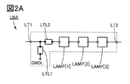
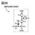
- 2A and 2B are block diagrams illustrating a configuration example of a circuit included in the semiconductor device.
- 3A to 3C are block diagrams illustrating a configuration example of a circuit included in the semiconductor device.
- FIG. 4 is a block diagram illustrating a configuration example of the semiconductor device.
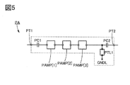
- FIG. 5 is a block diagram illustrating a configuration example of a circuit included in the semiconductor device.
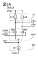
- 6A and 6B are block diagrams illustrating a configuration example of a circuit included in the semiconductor device, and
- FIG. 6C is a circuit diagram showing an example of a current source.
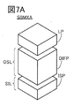
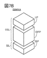
- 7A to 7D are perspective views illustrating a laminated structure of circuits included in a semiconductor device.
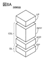
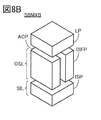
- FIG. 8A to 8C are perspective views illustrating a laminated structure of circuits included in a semiconductor device.
- 9A and 9B are block diagrams illustrating a configuration example of a circuit included in the semiconductor device.
- FIG. 10 is a schematic cross-sectional view illustrating a configuration example of the semiconductor device.
- FIG. 11 is a schematic cross-sectional view illustrating a configuration example of the semiconductor device.
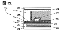
- 12A to 12C are schematic cross-sectional views illustrating a configuration example of the transistor.
- 13A and 13A are schematic cross-sectional views illustrating a configuration example of a transistor.
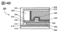
- 14A and 14B are schematic cross-sectional views illustrating a configuration example of a transistor.
- FIG. 15 is a schematic cross-sectional view illustrating a configuration example of the semiconductor device.
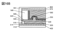
- FIG. 16A and 16B are schematic cross-sectional views illustrating a configuration example of a transistor.
- FIG. 17 is a schematic cross-sectional view illustrating a configuration example of the semiconductor device.
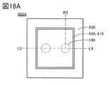
- FIG. 18A is a top view showing a configuration example of the capacitance
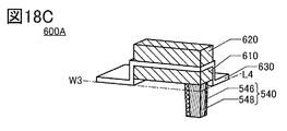
- FIGS. 18B and 18C are cross-sectional perspective views showing a configuration example of the capacitance.
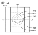
- 19A is a top view showing a configuration example of the capacitance
- FIG. 19B is a cross-sectional view showing a configuration example of the capacitance
- FIG. 19C is a sectional perspective view showing a configuration example of the capacitance.
- 20A is a diagram for explaining the classification of the crystal structure of IGZO, FIG.
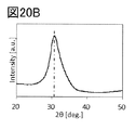
- FIG. 20B is a diagram for explaining the XRD spectrum of crystalline IGZO
- FIG. 20C is a microelectron diffraction pattern of crystalline IGZO. It is a figure explaining.
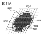
- 21A is a perspective view showing an example of a semiconductor wafer
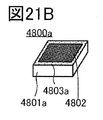
- FIG. 21B is a perspective view showing an example of a chip
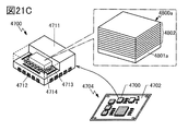
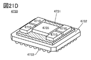
- FIGS. 21C and 21D are perspective views showing an example of an electronic component.
- FIG. 22 is a diagram showing the hierarchical structure of the IoT network and the tendency of the required specifications.
- FIG. 23 is an image diagram of factory automation.
- FIG. 24 is a perspective view showing an example of an electronic device.
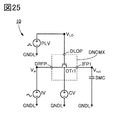
- FIG. 25 is a circuit diagram illustrating the conditions for circuit calculation.
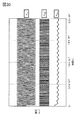
- FIG. 26 is a diagram illustrating the result of circuit calculation.
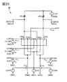
- FIG. 27 is a circuit diagram illustrating the conditions for circuit calculation.
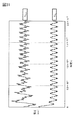
- FIG. 28 is a diagram illustrating the result of circuit calculation.
- FIG. 29 is a circuit diagram illustrating the conditions for circuit calculation.
- FIG. 30 is a diagram illustrating the result of circuit calculation.
- FIG. 31 is a diagram illustrating the result of circuit calculation.
- a metal oxide is a metal oxide in a broad sense. Metal oxides are classified into oxide insulators, oxide conductors (including transparent oxide conductors), oxide semiconductors (also referred to as Oxide Semiconductor or simply OS) and the like. For example, when a metal oxide is contained in the channel forming region of a transistor, the metal oxide may be referred to as an oxide semiconductor. That is, when a metal oxide can form a channel forming region of a transistor having at least one of an amplification action, a rectifying action, and a switching action, the metal oxide is referred to as a metal oxide semiconductor. Can be done. Further, when describing as an OS transistor, it can be paraphrased as a transistor having a metal oxide or an oxide semiconductor.
- a metal oxide having nitrogen may also be collectively referred to as a metal oxide. Further, a metal oxide having nitrogen may be referred to as a metal oxynitride.
- the configuration shown in each embodiment can be appropriately combined with the configuration shown in other embodiments to form one aspect of the present invention. Further, when a plurality of configuration examples are shown in one embodiment, the configuration examples can be appropriately combined with each other.
- the content (may be a part of the content) described in one embodiment is the other content (may be a part of the content) described in the embodiment and one or more other implementations. It is possible to apply, combine, or replace at least one content with the content described in the form of (may be a part of the content).
- the figure (which may be a part) described in one embodiment is different from another part of the figure, another figure (which may be a part) described in the embodiment, and one or more other figures.
- the figure (which may be a part) described in the embodiment is different from another part of the figure, another figure (which may be a part) described in the embodiment, and one or more other figures.
- FIG. 1 shows a configuration example of the high frequency receiver 100.
- the high frequency receiver 100 has, for example, an antenna ANT, a low noise amplifier LNA, a local oscillator LO, a down conversion mixer DNCMX, a bandpass filter BPF, an IF amplifier IFA, and an analog-to-digital conversion circuit ADC.
- the low noise amplifier LNA has a terminal LT1 that functions as an input terminal and a terminal LT2 that functions as an output terminal. Further, the down conversion mixer DNCMX has a terminal DRFP, a terminal DLOP, and a terminal IFP1.
- the antenna ANT is electrically connected to the terminal LT1 of the low noise amplifier LNA, and the terminal LT2 of the low noise amplifier LNA is electrically connected to the terminal DRFP of the down conversion mixer DNCMX.
- the terminal DLOP of the down conversion mixer DNCMX is electrically connected to the local oscillator LO, and the terminal IFP1 of the down conversion mixer DNCMX is electrically connected to the input terminal of the bandpass filter BPF.
- the input terminal of the IF amplifier IFA is electrically connected to the output terminal of the bandpass filter BPF, and the output terminal of the IF amplifier IFA is electrically connected to the input terminal of the analog-to-digital conversion circuit ADC.
- the output terminal of the analog-to-digital conversion circuit ADC is electrically connected to a logic circuit or the like provided in a semiconductor device (not shown).
- the antenna ANT has, for example, a function of converting the radio wave into an RF (Radio Frequency) signal when the antenna ANT receives a radio wave of a frequency used for a carrier wave of wireless communication from the outside.
- RF Radio Frequency
- the low noise amplifier LNA has a function of amplifying the voltage amplitude of the RF signal generated by the antenna ANT receiving radio waves from the outside, for example. Further, the low noise amplifier LNA has a function of reducing the noise of the amplified RF signal. The low noise amplifier LNA preferably has a filter function for removing noise in addition to the function for reducing noise.
- the low noise amplifier LNA can have the circuit configuration shown in FIG. 2A as an example.
- the low noise amplifier LNA shown in FIG. 2A has a configuration of a three-stage power amplifier.
- the low noise amplifier LNA of FIG. 2A has an amplifier LAMP [1] to an amplifier LAMP [3], a transmission line LTL1, and a transmission line LTL2.
- each of the amplifier LAMP [1] and the amplifier LAMP [3] has an input terminal and an output terminal.
- the terminal LT1 is electrically connected to the wiring GNDL via the transmission line LTL1. Further, the terminal LT1 is electrically connected to the input terminal of the amplifier LAMP [1] via the transmission line LTL2.
- the output terminal of the amplifier LAMP [1] is electrically connected to the input terminal of the amplifier LAMP [2], and the output terminal of the amplifier LAMP [2] is electrically connected to the input terminal of the amplifier LAMP [3].
- the output terminal of the amplifier LAMP [3] is electrically connected to the terminal LT2.
- Each of the transmission line LTL1 and the transmission line LTL2 is a wiring for transmitting an electric signal such as an RF signal, and has a parasitic resistance and a parasitic capacitance. Therefore, each of the transmission line LTL1 and the transmission line LTL2 has an input impedance, a characteristic impedance, and the like.
- each of the amplifier LAMP [1] and the amplifier LAMP [3] can have, for example, the circuit configuration shown in FIG. 2B.
- the amplifier AMP of FIG. 2B has a capacitance C1, a resistor R1, a transistor Str1, and a transmission line TL1 to a transmission line TL3.
- the input terminal of the amplifier AMP is electrically connected to the first terminal of the capacitance C1, and the second terminal of the capacitance C1 is electrically connected to the first terminal of the resistor R1 and the gate of the transistor Str1. ..
- the second terminal of the resistor R1 is electrically connected to the wiring VAL.
- the first terminal of the transistor Str1 is electrically connected to the wiring VDDL via the transmission line TL1 and the transmission line TL3, and the second terminal of the transistor Str1 is electrically connected to the wiring GNDL.
- the wiring VAL functions as a wiring that gives a constant voltage as an example.
- the constant voltage can be, for example, a high level potential (VDD), a potential higher than VDD, a potential lower than VDD, or the like.
- the wiring VDDL functions as a wiring for applying a constant voltage as an example.
- the constant voltage can be, for example, a high level potential (VDD).
- the wiring GNDL functions as a wiring for applying a constant voltage as an example.
- the constant voltage can be, for example, a low level potential, a ground potential (GND), or the like.
- the output terminal of the amplifier AMP is electrically connected to the connection portion between the transmission line TL1 and the transmission line TL3 via the transmission line TL2.
- the transmission line TL1 to the transmission line TL3 are wirings for transmitting an electric signal, similarly to the transmission line LTL1 and the transmission line LTL2. Therefore, the transmission line PTL1 has an input impedance, a characteristic impedance, and the like.
- the amplifier AMP has a function of amplifying the voltage amplitude of the electric signal input to the input terminal and outputting it to the output terminal. Further, the amplifier AMP has a function as an impedance matching circuit.
- the transistor Str1 for example, a transistor having silicon in the channel forming region (hereinafter, referred to as a Si transistor) is used.
- the silicon for example, amorphous silicon (sometimes called hydride amorphous silicon), single crystal silicon, microcrystalline silicon, polycrystalline silicon and the like can be used.
- the transistor Str1 includes, for example, a transistor in which Ge is included in the channel forming region, and a compound semiconductor such as ZnSe, CdS, GaAs, InP, GaN, and SiGe in the channel forming region. It can be a transistor, a transistor in which carbon nanotubes are contained in the channel forming region, a transistor in which an organic semiconductor is contained in the channel forming region, or the like.
- a low noise amplifier LNA can be configured by using the amplifier AMP shown in FIG. 2B.
- the local oscillator LO has a function of generating a signal for converting a voltage waveform.
- the conversion is performed by the town conversion mixer DNCMX described later.
- the down conversion mixer DNCMX mixes the RF signal input to the terminal DRFP with the signal transmitted from the local oscillator LO to the terminal DLOP to generate an electric signal lower than the frequency of the RF signal input to the terminal DRFP.
- Has the function of The generated electric signal is output to the terminal IFP1 as a signal having an intermediate frequency (Intermediate Frequency) (hereinafter referred to as an IF signal).
- the bandpass filter BPF has a function of outputting an AC voltage of a specific frequency band among the frequencies of the IF signal input to the input terminal of the bandpass filter BPF to the output terminal of the bandpass filter BPF. Further, the bandpass filter BPF has a function of attenuating an AC voltage other than the specific frequency band.
- the bandpass filter BPF can select one or more channels from an IF signal having a plurality of channels by determining a specific frequency band output to the output terminal.
- the IF amplifier IFA has a function of amplifying the voltage amplitude of the IF signal of the channel selected by the bandpass filter BPF.
- the analog-to-digital conversion circuit ADC has a function of converting the IF signal amplified by the IF amplifier IFA into a digital signal.
- the digital signal output from the analog-to-digital conversion circuit ADC is transmitted to, for example, a processing unit (not shown) electrically connected to the high frequency receiver 100.
- the processing unit may be configured to include, for example, a logic circuit that processes the digital signal.
- the radio wave received by the antenna ANT specifically, the radio wave of the frequency used for the carrier wave of wireless communication
- the processing unit can read out the information contained in the digital signal and perform processing based on the information.
- the low noise amplifier LNA applicable to the high frequency receiver 100 has a configuration in which the amplifier LAMP has three stages, but it may be two stages or four or more stages.
- the low noise amplifier LNA since the RF signal converted from the radio wave by the antenna ANT is weak, the low noise amplifier LNA reaches a level where the RF signal can be handled by the processing unit (for example, logic circuit) at the output destination of the analog-digital conversion circuit ADC. It is preferable to amplify the amplitude of the voltage.
- the low noise amplifier LNA has a configuration having a plurality of stages of amplifier LAMP.
- the circuit area of the low noise amplifier LNA increases, so that the occupied area of the high frequency receiver 100 may increase.
- the amplifier LAMP included in the low noise amplifier LNA increases, heat due to the current is generated by that amount, and the temperature of the high frequency receiver 100 may rise.
- the amplifier LAMP contains a Si transistor, the field effect mobility of the Si transistor decreases as the temperature rises, so that it becomes difficult for the amplifier LAMP to amplify the electric signal to a desired voltage amplitude.
- FIG. 3A shows an example of the circuit configuration of the down conversion mixer DNCMX1 that can be applied to the down conversion mixer DNCMX of FIG. Note that FIG. 3A shows not only the down-conversion mixer DNCMX but also a low-noise amplifier LNA and a local oscillator LO in order to explain the electrical connection with the circuits around the down-conversion mixer DNCMX.
- the down conversion mixer DNCMX1 shown in FIG. 3A has a transistor OTr1 which is an OS transistor.
- the transistor OTr1 functions as a pass transistor in the down conversion mixer DNCMX1.
- the first terminal of the transistor OTr1 is electrically connected to the terminal DRFP, the second terminal of the transistor OTr1 is electrically connected to the terminal IFP1, and the gate of the transistor OTr1 is electrically connected to the terminal DLOP. ..
- the OS transistor can be formed on a glass substrate, for example. Therefore, unlike the Si transistor, the OS transistor can have a configuration that does not have a bulk capacitance. As a result, the OS transistor is less susceptible to the decrease in operating frequency due to the bulk capacitance.
- the OS transistor can be arranged above the substrate on which the Si transistor is formed, as shown in FIG. 10 described in the third embodiment. That is, since the semiconductor device can be configured to have both an OS transistor and a Si transistor, the circuit of the semiconductor device can be configured so as to be suitable for the respective characteristics of the OS transistor and the Si transistor. it can. For example, in the same circuit of a semiconductor device, a Si transistor is applied as a transistor that allows a high on-current to flow, and an OS transistor is applied as a transistor whose electrical characteristics are unlikely to change due to temperature changes. It can be applied in the circuit.
- the OS transistor includes, for example, an SOI substrate, a quartz substrate, a plastic substrate, a sapphire glass substrate, a metal substrate, a stainless steel substrate, a substrate having a stainless steel still foil, a tungsten substrate, and a tungsten foil. It can be formed on a substrate having a substrate, a flexible substrate, a laminated film, a paper containing a fibrous material, a substrate film, or the like. Further, as an example of the glass substrate, there are barium borosilicate glass, aluminoborosilicate glass, soda lime glass and the like. Examples of flexible substrates, laminated films, base films, etc. include the following.
- plastics typified by polyethylene terephthalate (PET), polyethylene naphthalate (PEN), polyether sulfone (PES), and polytetrafluoroethylene (PTFE).
- PET polyethylene terephthalate
- PEN polyethylene naphthalate
- PES polyether sulfone
- PTFE polytetrafluoroethylene
- acrylic examples include polypropylene, polyester, polyvinyl fluoride, polyvinyl chloride, and the like.
- examples include polyamides, polyimides, aramids, epoxies, inorganic vapor-deposited films, and papers.
- the transistor OTr1 included in the down conversion mixer DNCMX1 may be a transistor having a back gate.
- the down conversion mixer DNCMX2 shown in FIG. 3B has a configuration in which a back gate is provided in the transistor OTr1 of the down conversion mixer DNCMX1, and the down conversion mixer DNCMX2 is the same as the down conversion mixer DNCMX1 in FIG. Can be applied to.
- the electrical connection destination of the back gate of the transistor OTr1 is not shown in FIG. 3B, the electrical connection destination of the back gate of the transistor OTr1 may be freely determined at the design stage of the high frequency receiver 100. ..
- the drive frequency of the transistor OTr1 can be increased and the current flowing when the transistor OTr1 is on can be increased.
- the back gate of the transistor OTr1 is provided with a wiring for electrically connecting to an external circuit, so that the external circuit gives a potential to the back gate of the transistor OTr1.
- the threshold voltage can be varied.
- the transistor described in other parts of the specification or the transistor shown in other drawings may also have a back gate. Further, in that case, the electrical connection of the back gate of the transistor may be freely determined as in the case of the transistor OTr1 as described above.
- some element or circuit for example, a passive element (for example, a passive element (for example, for example)) is formed between the terminal DRFP and the first terminal of the transistor OTr1. Resistors, capacitances, coils, transformers, etc.) and active elements (eg, transistors, etc.) may be connected. Similarly, for example, some element or circuit may be connected between the terminal IFP1 and the second terminal of the transistor OTr1. Further, for example, some element or circuit may be connected between the terminal DLOP and the gate of the transistor OTr1.
- a passive element for example, a passive element (for example, for example)
- active elements eg, transistors, etc.
- the down conversion mixer DNCMX3 shown in FIG. 3C as a circuit applicable to the down conversion mixer DNCMX in FIG. 1, there is a circuit between the terminal DRFP and the first terminal of the transistor OTr1 with respect to the down conversion mixer DNCMX1 in FIG. 3A.
- the circuit ANC1, the circuit ANC2, and the circuit ANC3 may be connected between the terminal IFP1 and the second terminal of the transistor OTr1 and between the terminal DLOP and the gate of the transistor OTr1.
- Each of the circuit ANC1 and the circuit ANC3 can be some kind of element or circuit.
- the high frequency receiver 100 has been described as an example of a semiconductor device including any one of the down conversion mixer DNCMX1 to the down conversion mixer DNCMX3 of FIGS. 3A to 3C.
- one aspect of the present invention includes this. Not limited.
- any one of the down conversion mixer DNCMX1 to the down conversion mixer DNCMX3 can be applied to a high frequency transmitter / receiver.
- FIG. 4 shows a configuration example of the high-frequency transmitter / receiver 200, which corresponds to the front end of an example radio of the FDD (Frequency Division Duplex) system, and the down-conversion mixer DNCMX included in the high-frequency transmitter / receiver 200 is ,
- the configurations of FIGS. 3A to 3C can be applied.
- the high frequency transmitter / receiver 200 will be described below. Regarding the high frequency transmitter / receiver 200, the description of the portion overlapping with the contents of the high frequency receiver 100 may be omitted.
- the high-frequency transmitter / receiver 200 has, for example, an antenna ANT, a duplexer DPXR, a low-noise amplifier LNA, a power amplifier PA, a local oscillator LO, a down-conversion mixer DNCMX, and an up-conversion mixer UPCMX.
- the duplexer DPXR has a terminal DT1, a terminal DT2, and a terminal DT3.
- the low noise amplifier LNA has a terminal LT1 that functions as an input terminal and a terminal LT2 that functions as an output terminal.
- the power amplifier PA has a terminal PT1 that functions as an input terminal and a PT2 that functions as an output terminal.
- the down conversion mixer DNCMX has a terminal DRFP, a terminal DLOP, and a terminal IFP1.
- the up-conversion mixer UPCMX has a terminal URFP, a terminal ULOP, and a terminal IFP2.
- the antenna ANT is electrically connected to the terminal DT1 of the duplexer DPXR.
- the terminal LT1 of the low noise amplifier LNA is electrically connected to the terminal DT2 of the duplexer DPXR, and the terminal LT2 of the low noise amplifier LNA is electrically connected to the terminal DRFP of the down conversion mixer DNCMX.
- the terminal PT1 of the power amplifier PA is electrically connected to the terminal URFP of the up-conversion mixer UPCMX, and the terminal PT1 of the power amplifier PA is electrically connected to the terminal DT3 of the duplexer DPXR.
- the local oscillator LO is electrically connected to the terminal DLOP of the down conversion mixer DNCMX and the terminal ULOP of the up conversion mixer UPCMX.
- the terminal IFP1 of the down conversion mixer DNCMX is electrically connected to a logic circuit or the like provided in a semiconductor device via a bandpass filter, an amplifier, an analog-digital conversion circuit, or the like (not shown).
- the terminal IFP2 of the up-conversion mixer UPCMX is electrically connected (not shown) to a logic circuit or the like provided in the semiconductor device as an example.
- the antenna ANT of the high-frequency transmitter / receiver 200 has a function of converting the radio wave into an RF signal when receiving a radio wave of a frequency used for a carrier wave of wireless communication, for example. Have. Further, the antenna ANT of the high frequency transmitter / receiver 200 has a function of converting the RF signal into radio waves having a frequency used for a carrier wave of wireless communication and transmitting the RF signal to the outside when the RF signal is input.
- the duplexer DPXR is a circuit used in an FDD type radio or the like, and has a function of electrically separating a signal path for transmission and a signal path for reception. Specifically, the duplexer DPXR makes the antenna ANT and the terminal LT1 of the low noise amplifier LNA conductive when the antenna ANT receives a radio signal from the outside, and connects the antenna ANT and the terminal PT2 of the power amplifier PA. It has a function to make the space non-conducting.
- the duplexer ANT makes a non-conducting state between the antenna ANT and the terminal LT1 of the low noise amplifier LNA, and the duplexer ANT and the terminal PT2 of the power amplifier PA are connected to each other. It has a function to make it conductive.
- the antenna ANT can be made into one antenna that shares the transmitting antenna and the receiving antenna.
- the power amplifier PA has a function of amplifying the voltage amplitude of the RF signal input to the input terminal and outputting the amplified electric signal to the output terminal.
- the antenna ANT can receive the RF signal amplified by the power amplifier PA and convert the RF signal into, for example, a radio wave.
- the power amplifier PA can have the circuit configuration shown in FIG. 5 as an example.
- the power amplifier PA shown in FIG. 5 has a configuration of a three-stage power amplifier.
- the power amplifier PA of FIG. 5 has an amplifier PAMP [1] to an amplifier PAMP [3], a capacitance PC1, a capacitance PC2, and a transmission line PTL1.
- the terminal PT1 is electrically connected to the first terminal of the capacitance PC1, and the second terminal of the capacitance PC2 is electrically connected to the input terminal of the amplifier PAMP [1]. Further, the output terminal of the amplifier PAMP [1] is electrically connected to the input terminal of the amplifier PAMP [2]. The output terminal of the amplifier PAMP [2] is electrically connected to the input terminal of the amplifier PAMP [3]. The output terminal of the amplifier PAMP [3] is electrically connected to the wiring GNDL via the transmission line PTL1. Further, the output terminal of the amplifier PAMP [3] is electrically connected to the first terminal of the capacitance PC2, and the second terminal of the capacitance PC2 is electrically connected to the terminal PT2.
- the transmission line PTL1 is a wiring for transmitting an electric signal, similarly to the transmission line LTL1 and the transmission line LTL2. Therefore, the transmission line PTL1 has an input impedance, a characteristic impedance, and the like.
- each configuration of the amplifier PAMP [1] to the amplifier PAMP [3] can be, for example, the amplifier AMP shown in FIG. 2B, similarly to the amplifier LAMP [1] to the amplifier LAMP [3]. That is, the power amplifier PA can be configured by using the amplifier AMP shown in FIG. 2B.
- the power amplifier PA has a configuration in which the amplifier PAMP has three stages, but it may have two stages or four or more stages.
- the local oscillator LO of the high frequency transmitter / receiver 200 has a function of generating a signal for converting a voltage waveform, similarly to the local oscillator LO of the high frequency receiver 100.
- the conversion is performed not only by the down conversion mixer DNCMX but also by the up conversion mixer UPCMX described later.
- the up-conversion mixer UPCMX mixes the IF signal input to the terminal IFP2 with the signal transmitted from the local oscillator LO to the terminal ULOP, and generates an electric signal higher than the frequency of the electric signal input to the terminal IFP2. Has the function of The generated electric signal is output to the terminal URFP as an RF signal.
- the electrical connection destination of the terminal IFP1 of the down conversion mixer DNCMX is not shown, but the IF signal output from the terminal IFP1 of the down conversion mixer DNCMX is a bandpass filter, an amplifier, and an analog-digital conversion circuit. For example, it is transmitted to the processing unit via the above.
- the radio wave received from the antenna ANT of the high frequency transmitter / receiver 200 (specifically, the radio wave having a frequency used for the carrier wave of wireless communication) is converted into a digital signal as a result.
- the processing unit can read out the information contained in the digital signal and perform processing based on the information.
- the terminal IFP2 of the up-conversion mixer UPCMX can be electrically connected to the processing unit via, for example, an amplifier, a digital-to-analog conversion circuit, or the like.
- the processing unit generates, for example, a digital signal including information to be transmitted from the antenna ANT, and converts the digital signal into an analog voltage by a digital-to-analog conversion circuit. Further, the analog voltage is converted into a voltage waveform by the up-conversion mixer UPCMX. Then, the converted analog voltage is transmitted to the antenna ANT via the power amplifier PA and the duplexer DPXR, and the antenna ANT converts the analog voltage into a radio wave having a frequency used as a carrier wave for wireless communication. As a result, the high frequency transmitter / receiver 200 can transmit information from the processing unit or the like to the outside as radio waves.
- a single balance domixer and a double balance domixer may be collectively referred to as a mixer.
- the term mixer can be rephrased as, for example, a mixer circuit, a mixing circuit, a mixer, a frequency mixing circuit, a frequency converter, a frequency conversion circuit, an analog multiplier, and the like.
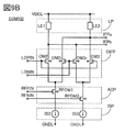
- FIG. 6A shows an example of a single-balanced mixer that can be applied to a down-conversion mixer DNCMX, an up-conversion mixer UPCMX, and the like.
- the single-balanced mixer SBMXA functions as a down-conversion mixer, for example, it has a function of mixing an RF signal of a single-phase signal and a differential signal from a local oscillator LO to generate an IF signal of the differential signal.
- the single-balanced mixer SBMXA has a function of mixing an IF signal and a differential signal from the local oscillator LO to generate an RF signal of the differential signal, for example, when functioning as an up-conversion mixer. ..
- the single-balanced mixer SBMXA of FIG. 6A has, for example, a transistor OM1, a transistor OM1r, a load LE1, a load LE2, and a current source IS1.
- the load LE1 and the load LE2 can be, for example, a resistor, an inductor, a diode, a transistor, or the like. Further, the load LE1 and the load LE2 may be, for example, a transistor driven in a linear region or a saturation region, a resistance changing element, an MTJ (magnetic tunnel junction) element, or the like. Further, the current mirror circuit may be configured by the load LE1 and the load LE2.
- the single-balanced mixer SBMXA does not provide either the load LE1 or the load LE2.
- the single-balanced mixer SBMXA does not provide the load LE2, and the wiring VDDL and the transistor.
- the configuration may be such that the first terminal of the OM1r is electrically connected.
- the transistor OM1 and the transistor OM1r are included in the differential section DIFP as an example, and the current source IS1 is included in the current source section ISP as an example.
- the LE1 and the load LE2 show the configuration included in the load unit LP as an example.
- the configuration of the single-balanced mixer SBMXA is not limited to the configuration shown in FIG. 6A.
- the single-balanced mixer SBMXA may have a configuration in which the load LE1 and the load LE2 are included in the differential section DIFP.
- the single-balanced mixer SBMXA may have a configuration in which the load LE1 and the load LE2 are included in the current source unit ISP.
- the first terminal of the load LE1 is electrically connected to the wiring VDDL, and the second terminal of the load LE1 is electrically connected to the first terminal of the transistor OM1 and the terminal IFPa. Further, the first terminal of the load LE2 is electrically connected to the wiring VDDL, and the second terminal of the load LE2 is electrically connected to the first terminal of the transistor OM1r and the terminal IFPb.
- the input terminal of the current source IS1 is electrically connected to the second terminal of the transistor OM1, the second terminal of the transistor OM1r, and the terminal RFP. Further, the output terminal of the current source IS1 is electrically connected to the wiring GNDL.
- the gate of the transistor OM1 is electrically connected to the terminal LOPIN. Further, the gate of the transistor OM1r is electrically connected to the terminal LONIN.
- the terminal LOPIN and the terminal LONIN correspond to the terminal DLOP of the down conversion mixer DNCMX in FIG.
- a signal from the local oscillator LO can be input to the terminal LOPIN.
- the voltage waveform of the signal can be, for example, a pulse voltage.
- a signal (a signal whose logic is inverted) having a phase difference of 180 degrees from the signal is input to the terminal LONIN.
- the terminal RFP corresponds to the terminal DRFP of the down conversion mixer DNCMX in FIG.
- the RF signal output from the output terminal of the low noise amplifier LNA can be input to the terminal RFPIN.
- the terminal IFPa and the terminal IFPb correspond to the terminal IFP1 of the down conversion mixer DNCMX in FIG. Therefore, the terminal IFPa and the terminal IFPb output the differential signal generated by the single-balanced mixer SBMXA as an IF signal.
- the single-balanced mixer SBMXA is configured to output an IF signal of a differential signal, the differential signal may be converted into a single-phase signal. Therefore, the single-balanced mixer SBMXA may have a configuration in which a differential single-phase conversion circuit (sometimes called a balanced unbalanced circuit or a high-frequency transformer) is electrically connected to the terminal IFPa and the terminal IFPb (not shown). .. With this configuration, the single-balanced mixer SBMXA can output a single-phase signal obtained by converting an IF signal which is a differential signal output from the terminal IFPa and the terminal IFPb.
- a differential single-phase conversion circuit sometimes called a balanced unbalanced circuit or a high-frequency transformer
- the load unit LP causes a current to flow from the second terminal of the load LE1 to the first terminal of the transistor OM1 by the voltage supplied from the wiring VDDL, and also from the second terminal of the load LE2 to the first terminal of the transistor OM1r. Has a function of passing an electric current through.
- the current source IS1 has a function of passing a constant current from an input terminal to an output terminal.
- the current source IS1 for example, the current source IS shown in FIG. 6C can be applied.
- the current source IS has a transistor Itr, a terminal VI, a terminal VO, and a terminal VB.
- the first terminal of the transistor Itr is electrically connected to the terminal VI
- the second terminal of the transistor Itr is electrically connected to the terminal VO
- the gate of the transistor Itr is electrically connected to the terminal VB. ..
- the terminal VI is electrically connected to, for example, the differential portion DIFP of the single-balanced mixer SBMXA and the terminal RFP
- the terminal VO is electrically connected to, for example, the wiring GNDL.
- the constant voltage can be, for example, a high level potential, a potential higher than the ground potential (GND), or the like.
- the differential unit DIFF generates a signal having a voltage waveform corresponding to the voltage waveform of the RF signal input from the terminal RFP and the voltage waveform of the signal input from the terminal LOPIN, and generates the signal. It has a function to output to the terminal IFPa. Further, as an example, the differential unit DIFF generates a signal having a voltage waveform corresponding to the voltage waveform of the RF signal input from the terminal RFP and the voltage waveform of the signal input from the terminal LONIN. It has a function to output a signal to the terminal IFPb.
- the transistor OM1 generates a signal having a frequency corresponding to the product, sum, difference, etc. of the frequency of the RF signal input from the terminal RFP and the frequency of the signal input from the terminal LOPIN.
- the signal is output to the terminal IFPa.
- the transistor OM1r generates a signal having a frequency corresponding to the product, sum, difference, etc. of the frequency of the RF signal input from the terminal RFP and the frequency of the signal input from the terminal LONIN, and outputs the signal to the terminal.
- Output to IFPb The differential signal output from the terminal IFPa and the terminal IFPb becomes the IF signal output by the single-balanced mixer SBMXA.
- the single-balanced mixer since the single-balanced mixer has a plurality of circuit elements such as transistors in the load unit, the current source unit, and the differential unit, the single-balanced mixer may become large. Therefore, in the single-balanced mixer SBMXA, for example, as shown in FIG. 7A, consider a configuration in which the differential section DIFF is provided above the current source section ISP and the load section LP is provided above the differential section DIFF. .. In particular, it is assumed that the layer SIL includes the current source unit ISP and the layer OSL includes the differential unit DIFF. The area occupied by the single-balanced mixer SBMXA can be reduced by forming the single-balanced mixer SBMXA in which the current source unit ISP, the differential unit DIFF, and the load unit LP are laminated.
- the transistor contained in the layer OSL is, for example, an OS transistor
- the transistor contained in the layer SIL is, for example, a Si transistor. That is, it is preferable to apply an OS transistor as the transistor OM1 and the transistor OM1r, and to apply a Si transistor as the transistor (for example, the transistor Itr) included in the current source ISP.
- an OS transistor as the transistor OM1 and the transistor OM1r
- a Si transistor as the transistor (for example, the transistor Itr) included in the current source ISP.
- the single-balanced mixer shown in the schematic diagram shown in FIG. 7A can be configured. The stacking of the OS transistor formed above the Si transistor will be described in detail in the third embodiment.
- the single-balanced mixer SBMXA of FIG. 6A is not limited to the laminated structure shown in FIG. 7A.
- the load unit LP may be included in the layer OSL as shown in FIG. 7B.
- the load unit LP may be included in the layer SIL as shown in FIG. 7C.
- the load unit LP is provided above the differential unit DIFF, but the load unit LP is provided above the current source unit ISP, and the differential unit DIFF is provided above the load unit LP. May be provided (not shown). Further, for example, in FIG.
- the current source unit ISP is provided above the load unit LP, but the load unit LP is provided above the current source unit ISP, and the differential unit DIFF is provided above the load unit LP. May be provided (not shown).
- the layer SIL may be configured so that the current source portion ISP and the load portion LP are not stacked on each other.
- the layer OSL may be configured so that the differential portion DIFP and the load portion LP are not stacked on each other (not shown).
- the single balance domixer SBMXB will be described below. The description of the portion of the single-balanced mixer SBMXB that overlaps with that of the single-balanced mixer SBMXA will be omitted.
- the single-balanced mixer SBMXB has a configuration of an active single-balanced mixer, and has a configuration in which a circuit unit ACP is provided on the single-balanced mixer SBMXA.
- the circuit unit ACP has a transistor RFOM, and the first terminal of the transistor RFOM is electrically connected to the second terminal of the transistor OM1 and the second terminal of the transistor OM1r.
- the second terminal of the RFOM is electrically connected to the input terminal of the current source IS1, and the gate of the transistor RFOM is electrically connected to the terminal RFP.
- the configuration of the single-balanced mixer SBMXB is not limited to the configuration shown in FIG. 6B.
- the single-balanced mixer SBMXB may have, for example, a configuration in which the transistor RFOM is included in the differential section DIFP, or may be a configuration in which the transistor RFOM is included in the current source section ISP, for example.
- the single-balanced mixer SBMXB is made into a single structure in which the current source unit ISP, the circuit unit ACP, the differential unit DIFF, and the load unit LP are laminated.
- the circuit area of the balanced mixer SBMXB can be reduced.
- the single-balanced mixer SBMXB is provided with a circuit section ACP above the current source section ISP, and a differential section DIFF is provided above the circuit section ACP.
- the load unit LP may be provided above the unit DIFF.
- the transistor contained in the layer SIL is applied to the Si transistor, and the layer OSL is formed. It is preferable to apply the included transistor to the OS transistor. That is, it is preferable to apply an OS transistor as the transistor OM1, the transistor OM1r, and the transistor RFOM, and to apply the Si transistor as the transistor (for example, the transistor Itr) included in the current source ISP.
- the single-balanced mixer SBMXB of FIG. 6B is not limited to the laminated structure shown in FIG. 8A.
- the circuit unit ACP is included in the layer OSL.
- the circuit unit ACP is provided above the current source unit ISP, and the circuit unit ACP and the current source unit ISP are included in the layer SIL. It may be configured (not shown). That is, an OS transistor may be applied as the transistor OM1 and the transistor OM1r, and a Si transistor may be applied as the transistor and the transistor RFOM included in the current source ISP.
- the layer OSL may be configured so that the circuit unit ACP and the differential unit DIFP are not stacked on each other.
- the layer SIL may be configured so that the circuit unit ACP and the current source unit ISP are not stacked on each other.
- FIG. 9A shows an example of a double-balanced mixer that can be applied to the down-conversion mixer DNCMX and the up-conversion mixer UPCMX.
- the double-balanced mixer DBMXA functions as a down-conversion mixer, for example, it has a function of mixing an RF signal of a differential signal and a differential signal from a local oscillator LO to generate an IF signal of the differential signal.
- the double-balanced mixer DBMXA has a function of mixing an IF signal and a differential signal from the local oscillator LO to generate an RF signal of the differential signal when functioning as an up-conversion mixer, for example. ..
- the double-balanced mixer DBMXA has a transistor OM2, a transistor OM2r, a transistor OM3, a transistor OM3r, a load LE1, a load LE2, a current source IS2, and a current source IS3.
- load LE1 and load LE2 For load LE1 and load LE2, the description of load LE1 and load LE2 possessed by the single-balanced mixer SBMXA is taken into consideration.
- the double-balanced mixer DBMXA does not provide either the load LE1 or the load LE2.
- the double-balanced mixer DBMXA does not provide the load LE2, and the wiring VDDL and the transistor.
- the configuration may be such that the first terminal of the OM2r and the first terminal of the transistor OM3 are electrically connected.
- the transistor OM2, the transistor OM2r, the transistor OM3, and the transistor OM3r are included in the differential unit DIFP as an example, and the current source IS2 and the current source IS3 are included.
- the load LE1 and the load LE2 are included in the load unit LP as an example.
- the double-balanced mixer DBMXB may have a configuration in which the load LE1 and / or the load LE2 are included in the differential section DIFP, may be included in the current source section ISP, or may be differential. The configuration may not be included in both the part DIFF and the current source part ISP.
- the first terminal of the load LE1 is electrically connected to the wiring VDDL, and the second terminal of the load LE1 is electrically connected to the first terminal of the transistor OM2, the first terminal of the transistor OM3r, and the terminal IFPb. Has been done.
- the first terminal of the load LE2 is electrically connected to the wiring VDDL, and the second terminal of the load LE2 is electrically connected to the first terminal of the transistor OM3, the first terminal of the transistor OM2r, and the terminal IFPa. Has been done.
- the input terminal of the current source IS2 is electrically connected to the second terminal of the transistor OM2, the second terminal of the transistor OM2r, and the terminal RFPIN. Further, the output terminal of the current source IS2 is electrically connected to the wiring GNDL.
- the input terminal of the current source IS3 is electrically connected to the second terminal of the transistor OM3, the second terminal of the transistor OM3r, and the terminal RFNIN. Further, the output terminal of the current source IS3 is electrically connected to the wiring GNDL.
- the gate of the transistor OM2 and the gate of the transistor OM3 are electrically connected to the terminal LOPIN. Further, the gate of the transistor OM2r and the gate of the transistor OM3r are electrically connected to the terminal LONIN.
- the terminal RFPIN and the terminal RFNIN correspond to the terminal DRFP of the down conversion mixer DNCMX in FIG.
- an RF signal of a differential signal is input to the terminal RFPIN and the terminal RFNIN.
- the signal input to the terminal RFNIN can be a signal whose phase of the signal input to the terminal RFPIN is advanced (or delayed) by half a wavelength.
- This differential signal can be generated by, for example, an RF signal of a single-phase signal generated by a low-noise amplifier LNA by a single-phase differential conversion circuit (balanced unbalanced circuit, sometimes called a high-frequency transformer).
- the double-balanced mixer DBMXA may have a configuration in which a single-phase differential conversion circuit is electrically connected to the terminal RFPIN and the terminal RFNIN (not shown).
- the RF signal of the single-phase signal generated by the low noise amplifier LNA can be converted into a differential signal, and the differential signal can be input to the terminal RFPIN and the terminal RFNIN.
- a single-phase RF signal output from the output terminal of the low noise amplifier LNA is input to the terminal RFPIN, and a ground potential is input to the terminal RFNIN. It may be configured to be used.
- terminal LOPIN terminal LONIN, terminal IFPa, and terminal IFPb
- terminal LOPIN terminal LONIN, terminal IFPa, and terminal IFPb
- terminal LOPIN terminal LONIN, terminal IFPa, and terminal IFPb of the single-balanced mixer SBMXA.
- the load unit LP causes a current to flow from the second terminal of the load LE1 to the first terminal of the transistor OM2 and the first terminal of the transistor OM3r by the voltage supplied from the wiring VDDL, and also causes the second terminal of the load LE2. It has a function of passing a current through the first terminal of the transistor OM2r and the first terminal of the transistor OM3.
- the current source IS2 and the current source IS3 have a function of passing a constant current from the input terminal to the output terminal.
- the current source IS2 and the current source IS3 for example, the current source IS shown in FIG. 6C can be applied.
- the transistor OM2 has a signal having a voltage waveform corresponding to the voltage waveform of the signal input from the terminal RFPIN and the voltage waveform of the signal input from the terminal LOPIN (here, the first signal). It has a function of generating (called a signal). Further, as an example, the transistor OM2r is a signal having a voltage waveform corresponding to the voltage waveform of the signal input from the terminal RFPIN and the voltage waveform of the signal input from the terminal LONIN (here, referred to as a second signal). ) Has a function to generate.
- the transistor OM3 is, for example, a signal having a voltage waveform corresponding to the voltage waveform of the signal input from the terminal RFNIN and the voltage waveform of the signal input from the terminal LOPIN (here, referred to as a third signal). ) Has a function to generate. Further, as an example, the transistor OM3r has a voltage waveform corresponding to the voltage waveform of the signal input from the terminal RFNIN and the voltage waveform of the signal input from the terminal LONIN (here, referred to as a fourth signal). ) Has a function to generate.
- the first signal is, for example, a signal having a frequency corresponding to the product, sum, difference, etc. of the frequency of the signal input from the terminal RFPIN and the frequency of the signal input from the terminal LOPIN. be able to.
- the second signal may be, for example, a signal having a frequency corresponding to the product, sum, difference, etc. of the frequency of the signal input from the terminal RFPIN and the frequency of the signal input from the terminal LONIN.
- the third signal can be, for example, a signal having a frequency corresponding to the product, sum, difference, etc. of the frequency of the signal input from the terminal RFNIN and the frequency of the signal input from the terminal LOPIN.
- the fourth signal can be, for example, a signal having a frequency corresponding to the product, sum, difference, etc. of the frequency of the signal input from the terminal RFNIN and the frequency of the signal input from the terminal LONIN.
- the frequency conversion can be determined according to, for example, the configuration of the load unit LP.
- the differential unit DIFF outputs the second signal and the third signal to the terminal IFPa as the first output signal, and outputs the first signal and the fourth signal to the terminal IFPb as the second output signal.
- the first output signal and the second output signal correspond to the IF signal of the differential signal output from the terminal IFP1 of the down conversion mixer DNCMX of FIG.
- the double-balanced mixer DBMXA is configured to output an IF signal of a differential signal, the differential signal may be converted into a single-phase signal. Therefore, the double-balanced mixer DBMXA may have a configuration in which a differential single-phase conversion circuit is electrically connected to the terminal IFPa and the terminal IFPb (not shown). With this configuration, the double-balanced mixer DBMXA can output a single-phase signal obtained by converting an IF signal which is a differential signal output from the terminal IFPa and the terminal IFPb.
- the double-balanced mixer DBMXA can have a configuration in which a differential section DIFF and a current source section ISP are laminated in order to reduce the circuit area.
- the laminated structure of the tabular balance domixer DBMXA has a configuration in which the differential transistor DIFP is included in the layer OSL and the current source transistor ISP is included in the layer SIL as shown in FIG. 7A
- the differential transistor An OS transistor is applied as the transistor OM2, the transistor OM2r, the transistor OM3, and the transistor OM3r included in the DIFP
- the Si transistor is used as the transistor (for example, the transistor Itr) included in the current source IS2 and the current source IS3. Can be applied.
- Double-balanced mixer DBMXA of FIG. 9A As the double-balanced mixer applicable to the down-conversion mixer DNCMX, for example, the double-balanced mixer DBMXB shown in FIG. 9B may be used. Further, as the double-balanced mixer that can be applied to the up-conversion mixer UPCMX, for example, the double-balanced mixer DBMXB shown in FIG. 9B may be used.
- the table balance domixer DBMXB will be described below. The description of the portion of the double-balanced mixer DBMXB that overlaps with that of the double-balanced mixer DBMXA will be omitted.
- the double-balanced mixer DBMXB has a configuration of an active double-balanced mixer, and has a configuration in which a circuit unit ACP is provided on the double-balanced mixer DBMXA.
- the circuit unit ACP has a transistor RFOM1 and a transistor RFOM2.
- the first terminal of the transistor RFOM1 is electrically connected to the second terminal of the transistor OM2 and the second terminal of the transistor OM2r, and the second terminal of the transistor RFOM1 is electrically connected to the input terminal of the current source IS2.
- the gate of the transistor RFOM1 is electrically connected to the terminal RFPIN.
- the first terminal of the transistor RFOM2 is electrically connected to the second terminal of the transistor OM3 and the second terminal of the transistor OM3r, and the second terminal of the transistor RFOM2 is electrically connected to the input terminal of the current source IS3.
- the gate of the transistor RFOM2 is electrically connected to the terminal RFNIN.
- the configuration of the double-balanced mixer DBMXB is not limited to the configuration shown in FIG. 9B.
- the double-balanced mixer DBMXB may have, for example, a configuration in which the transistor RFOM1 and / or the transistor RFOM2 is included in the differential section DIFP, and for example, the transistor RFOM1 and / or the transistor RFOM2 is included in the current source section ISP.
- the configuration may be.
- the double-balanced mixer DBMXB is doubled by having the current source unit ISP, the circuit unit ACP, the differential unit DIFF, and the load unit LP laminated.
- the circuit area of the balanced mixer DBMXB can be reduced.
- the layer SIL includes the current source unit ISP and the layer OSL includes the circuit unit ACP and the differential unit DIFF, as shown in FIG. 8A
- the layer It is preferable to apply the transistor contained in the SIL to the Si transistor and the transistor contained in the layer OSL to the OS transistor. That is, an OS transistor is applied as the transistor OM2, the transistor OM2r, the transistor OM3, the transistor OM3r, the transistor RFOM1, and the transistor RFOM2, and the Si transistor is applied as the transistor (for example, the transistor Itr) included in the current source ISP. It is preferable to do so.
- the layer SIL includes the circuit unit ACP and the current source unit ISP
- the layer OSL includes the differential unit DIFF
- the semiconductor device shown in FIG. 10 includes a transistor 300, a transistor 500, and a capacitive element 600.
- 12A is a cross-sectional view of the transistor 500 in the channel length direction
- FIG. 12B is a cross-sectional view of the transistor 500 in the channel width direction
- FIG. 12C is a cross-sectional view of the transistor 300 in the channel width direction.
- Transistor 500 is an OS transistor.
- the transistor 500 has a characteristic that the off-current is small and the field effect mobility does not easily change even at a high temperature.
- a transistor 500 as a transistor included in a semiconductor device, for example, a high-frequency receiver 100 or a down-conversion mixer DNCMX of a high-frequency transmitter / receiver 200, it is possible to realize a semiconductor device whose operating ability is not significantly reduced even at high temperatures.
- the semiconductor device described in this embodiment includes a transistor 300, a transistor 500, and a capacitive element 600 as shown in FIG.
- the transistor 500 is provided above the transistor 300, for example, and the capacitive element 600 is provided above the transistor 300 and the transistor 500, for example.
- the capacitance element 600 can be the capacitance included in the high-frequency receiver 100 or the high-frequency transmitter / receiver 200 described in the above embodiment. Depending on the configuration of the high-frequency receiver 100 or the high-frequency transmitter / receiver 200, the capacitive element 600 shown in FIG. 10 may not necessarily be provided.
- the transistor 300 is provided on the substrate 311 and has a semiconductor region 313 composed of a conductor 316, an insulator 315, and a part of the substrate 311, a low resistance region 314a functioning as a source region or a drain region, and a low resistance region 314b. ..
- the transistor 300 can be applied to, for example, a transistor included in the high frequency receiver 100 or the high frequency transmitter / receiver 200 described in the above embodiment. Specifically, for example, it may be a transistor included in a bandpass filter BPF, an IF amplifier IFA, an analog-digital conversion circuit ADC, a local oscillator LO, or the like. Note that FIG.
- FIG. 10 shows a configuration in which the gate of the transistor 300 is electrically connected to one of the source and drain of the transistor 500 via one of the pair of electrodes of the capacitive element 600, but high frequency reception Depending on the configuration of the machine 100 or the high frequency transmitter / receiver 200, one of the source or drain of the transistor 300 is electrically connected to one of the source or drain of the transistor 500 via one of the pair of electrodes of the capacitive element 600. In addition, one of the source and drain of the transistor 300 may be electrically connected to the gate of the transistor 500 via one of the pair of electrodes of the capacitive element 600.
- a semiconductor substrate for example, a single crystal substrate or a silicon substrate
- the substrate 311 it is preferable to use a semiconductor substrate (for example, a single crystal substrate or a silicon substrate) as the substrate 311.
- the transistor 300 has the upper surface of the semiconductor region 313 and the side surface in the channel width direction covered with the conductor 316 via the insulator 315.
- the on-characteristics of the transistor 300 can be improved by increasing the effective channel width. Further, since the contribution of the electric field of the gate electrode can be increased, the off characteristic of the transistor 300 can be improved.
- the transistor 300 may be either a p-channel type or an n-channel type.
- a semiconductor such as a silicon-based semiconductor in a region in which a channel of the semiconductor region 313 is formed, a region in the vicinity thereof, a low resistance region 314a serving as a source region or a drain region, a low resistance region 314b, and the like.
- It preferably contains crystalline silicon.
- it may be formed of a material having Ge (germanium), SiGe (silicon germanium), GaAs (gallium arsenide), GaAlAs (gallium aluminum arsenide), or the like.
- a configuration using silicon in which the effective mass is controlled by applying stress to the crystal lattice and changing the lattice spacing may be used.
- the transistor 300 may be a HEMT (High Electron Mobility Transistor) by using GaAs and GaAlAs or the like.
- an element that imparts n-type conductivity such as arsenic and phosphorus, or a p-type conductivity such as boron is imparted.
- the conductor 316 that functions as a gate electrode is a semiconductor material such as silicon, a metal material, or an alloy that contains an element that imparts n-type conductivity such as arsenic or phosphorus, or an element that imparts p-type conductivity such as boron.
- a material or a conductive material such as a metal oxide material can be used.
- the threshold voltage of the transistor can be adjusted by selecting the material of the conductor. Specifically, it is preferable to use a material such as titanium nitride or tantalum nitride for the conductor. Further, in order to achieve both conductivity and embedding property, it is preferable to use a metal material such as tungsten or aluminum as a laminate for the conductor, and it is particularly preferable to use tungsten in terms of heat resistance.
- the transistor 300 shown in FIG. 10 is an example, and the transistor 300 is not limited to its structure, and an appropriate transistor may be used according to the circuit configuration and the driving method.
- the transistor 300 may be configured in the same manner as the transistor 500 using an oxide semiconductor, as shown in FIG. The details of the transistor 500 will be described later.
- An insulator 320, an insulator 322, an insulator 324, and an insulator 326 are laminated in this order so as to cover the transistor 300.
- the insulator 320, the insulator 322, the insulator 324, and the insulator 326 for example, silicon oxide, silicon oxide nitride, silicon nitride oxide, silicon nitride, aluminum oxide, aluminum oxide nitride, aluminum nitride, aluminum nitride and the like can be used. Just do it.
- silicon oxide refers to a material whose composition has a higher oxygen content than nitrogen
- silicon nitride refers to a material whose composition has a higher nitrogen content than oxygen. Is shown.
- aluminum nitride refers to a material whose composition has a higher oxygen content than nitrogen
- aluminum nitride refers to a material whose composition has a higher nitrogen content than oxygen. Is shown.
- the insulator 322 may have a function as a flattening film for flattening a step generated by a transistor 300 or the like provided below the insulator 322.
- the upper surface of the insulator 322 may be flattened by a flattening treatment using a chemical mechanical polishing (CMP) method or the like in order to improve the flatness.
- CMP chemical mechanical polishing
- the insulator 324 it is preferable to use a film having a barrier property so that hydrogen and impurities do not diffuse in the region where the transistor 500 is provided from the substrate 311 or the transistor 300.
- a film having a barrier property against hydrogen for example, silicon nitride formed by the CVC method can be used.
- hydrogen may diffuse into a semiconductor element having an oxide semiconductor such as a transistor 500, so that the characteristics of the semiconductor element may deteriorate. Therefore, it is preferable to use a film that suppresses the diffusion of hydrogen between the transistor 500 and the transistor 300.
- the membrane that suppresses the diffusion of hydrogen is a membrane that desorbs a small amount of hydrogen.
- the amount of hydrogen desorbed can be analyzed using, for example, a heated desorption gas analysis method (TDS).
- TDS heated desorption gas analysis method
- the amount of hydrogen desorbed from the insulator 324 is the amount desorbed in terms of hydrogen atoms when the surface temperature of the film is in the range of 50 ° C. to 500 ° C. It may be 10 ⁇ 10 15 atoms / cm 2 or less, preferably 5 ⁇ 10 15 atoms / cm 2 or less.
- the insulator 326 has a lower dielectric constant than the insulator 324.
- the relative permittivity of the insulator 326 is preferably less than 4, more preferably less than 3.
- the relative permittivity of the insulator 326 is preferably 0.7 times or less, more preferably 0.6 times or less, the relative permittivity of the insulator 324.
- the capacitance element 600, the conductor 328 connected to the transistor 500, the conductor 330, and the like are embedded.
- the conductor 328 and the conductor 330 have a function as a plug or wiring.
- a conductor having a function as a plug or wiring may collectively give a plurality of structures the same reference numerals.
- the wiring and the plug connected to the wiring may be integrated. That is, a part of the conductor may function as a wiring, and a part of the conductor may function as a plug.
- each plug and wiring As the material of each plug and wiring (conductor 328, conductor 330, etc.), a conductive material such as a metal material, an alloy material, a metal nitride material, or a metal oxide material is used as a single layer or laminated. be able to. It is preferable to use a refractory material such as tungsten or molybdenum that has both heat resistance and conductivity, and it is preferable to use tungsten. Alternatively, it is preferably formed of a low resistance conductive material such as aluminum or copper. Wiring resistance can be reduced by using a low resistance conductive material.
- a wiring layer may be provided on the insulator 326 and the conductor 330.
- the insulator 350, the insulator 352, and the insulator 354 are laminated in this order.
- a conductor 356 is formed on the insulator 350, the insulator 352, and the insulator 354.
- the conductor 356 has a function as a plug or wiring for connecting to the transistor 300.
- the conductor 356 can be provided by using the same material as the conductor 328 and the conductor 330.
- the insulator 350 it is preferable to use an insulator having a barrier property against hydrogen, like the insulator 324.
- the conductor 356 preferably contains a conductor having a barrier property against hydrogen.
- a conductor having a barrier property against hydrogen is formed in the opening of the insulator 350 having a barrier property against hydrogen.
- the conductor having a barrier property against hydrogen for example, tantalum nitride or the like may be used. Further, by laminating tantalum nitride and tungsten having high conductivity, it is possible to suppress the diffusion of hydrogen from the transistor 300 while maintaining the conductivity as wiring. In this case, it is preferable that the tantalum nitride layer having a barrier property against hydrogen has a structure in contact with the insulator 350 having a barrier property against hydrogen.
- a wiring layer may be provided on the insulator 354 and the conductor 356.
- the insulator 360, the insulator 362, and the insulator 364 are laminated in this order.
- a conductor 366 is formed on the insulator 360, the insulator 362, and the insulator 364.
- the conductor 366 has a function as a plug or wiring.
- the conductor 366 can be provided by using the same material as the conductor 328 and the conductor 330.
- the insulator 360 it is preferable to use an insulator having a barrier property against hydrogen, like the insulator 324.
- the conductor 366 preferably contains a conductor having a barrier property against hydrogen.
- a conductor having a barrier property against hydrogen is formed in the opening of the insulator 360 having a barrier property against hydrogen.
- a wiring layer may be provided on the insulator 364 and the conductor 366.
- the insulator 370, the insulator 372, and the insulator 374 are laminated in this order.
- a conductor 376 is formed on the insulator 370, the insulator 372, and the insulator 374.
- the conductor 376 has a function as a plug or wiring.
- the conductor 376 can be provided by using the same material as the conductor 328 and the conductor 330.
- the insulator 370 it is preferable to use an insulator having a barrier property against hydrogen, similarly to the insulator 324.
- the conductor 376 preferably contains a conductor having a barrier property against hydrogen.
- a conductor having a barrier property against hydrogen is formed in the opening of the insulator 370 having a barrier property against hydrogen.
- a wiring layer may be provided on the insulator 374 and the conductor 376.
- the insulator 380, the insulator 382, and the insulator 384 are laminated in this order.
- a conductor 386 is formed on the insulator 380, the insulator 382, and the insulator 384.
- the conductor 386 has a function as a plug or wiring.
- the conductor 386 can be provided by using the same material as the conductor 328 and the conductor 330.
- the insulator 380 it is preferable to use an insulator having a barrier property against hydrogen, like the insulator 324.
- the conductor 386 preferably contains a conductor having a barrier property against hydrogen.
- a conductor having a barrier property against hydrogen is formed in the opening of the insulator 380 having a barrier property against hydrogen.
- the semiconductor device according to the present embodiment has been described. It is not limited to this.
- the number of wiring layers similar to the wiring layer containing the conductor 356 may be three or less, or the number of wiring layers similar to the wiring layer including the conductor 356 may be five or more.
- Insulator 510, insulator 512, insulator 514, and insulator 516 are laminated in this order on the insulator 384.
- any of the insulator 510, the insulator 512, the insulator 514, and the insulator 516 it is preferable to use a substance having a barrier property against oxygen and hydrogen.
- a film having a barrier property so that hydrogen and impurities do not diffuse from the area where the substrate 311 or the transistor 300 is provided to the area where the transistor 500 is provided is used. Is preferable. Therefore, the same material as the insulator 324 can be used.
- Silicon nitride formed by the CVD method can be used as an example of a film having a barrier property against hydrogen.
- hydrogen may diffuse into a semiconductor element having an oxide semiconductor such as a transistor 500, so that the characteristics of the semiconductor element may deteriorate. Therefore, it is preferable to use a film that suppresses the diffusion of hydrogen between the transistor 500 and the transistor 300.
- the membrane that suppresses the diffusion of hydrogen is a membrane that desorbs a small amount of hydrogen.
- metal oxides such as aluminum oxide, hafnium oxide, and tantalum oxide for the insulator 510 and the insulator 514.
- aluminum oxide has a high blocking effect that does not allow the membrane to permeate both oxygen and impurities such as hydrogen and water, which are factors that change the electrical characteristics of transistors. Therefore, aluminum oxide can prevent impurities such as hydrogen and water from being mixed into the transistor 500 during and after the manufacturing process of the transistor. In addition, the release of oxygen from the oxides constituting the transistor 500 can be suppressed. Therefore, it is suitable for use as a protective film for the transistor 500.
- the same material as the insulator 320 can be used for the insulator 512 and the insulator 516. Further, by applying a material having a relatively low dielectric constant to these insulators, it is possible to reduce the parasitic capacitance generated between the wirings.
- a silicon oxide film, a silicon nitride film, or the like can be used as the insulator 512 and the insulator 516.
- a conductor 518 a conductor constituting the transistor 500 (for example, a conductor 503) and the like are embedded.
- the conductor 518 has a function as a plug or wiring for connecting to the capacitance element 600 or the transistor 300.
- the conductor 518 can be provided by using the same material as the conductor 328 and the conductor 330.
- the conductor 510 and the conductor 518 in the region in contact with the insulator 514 are preferably conductors having a barrier property against oxygen, hydrogen, and water.
- the transistor 300 and the transistor 500 can be separated by a layer having a barrier property against oxygen, hydrogen, and water, and the diffusion of hydrogen from the transistor 300 to the transistor 500 can be suppressed.
- a transistor 500 is provided above the insulator 512.
- the transistor 500 includes a conductor 503 arranged so as to be embedded in the insulator 514 and the insulator 516, and an insulator arranged on the insulator 516 and the insulator 503.
- 520 insulator 522 placed on insulator 520
- insulator 524 placed on insulator 522
- oxide 530a placed on insulator 524
- oxide 530a oxide 530b
- the oxide 530b arranged on the oxide 530b, the conductor 542a and the conductor 542b arranged apart from each other on the oxide 530b, and the conductor 542a and the conductor 542b arranged on the conductor 542a and the conductor 542b.
- the oxide 530c arranged on the bottom surface and the side surface of the opening, the insulator 550 arranged on the forming surface of the oxide 530c, and the forming surface of the insulator 550. It has an arranged conductor 560 and.
- the insulator 544 is arranged between the oxide 530a, the oxide 530b, the conductor 542a, and the conductor 542b, and the insulator 580.
- the conductor 560 includes a conductor 560a provided inside the insulator 550 and a conductor 560b provided so as to be embedded inside the conductor 560a. It is preferable to have.
- the insulator 574 is arranged on the insulator 580, the conductor 560, and the insulator 550.
- oxide 530a, oxide 530b, and oxide 530c may be collectively referred to as oxide 530.
- the transistor 500 shows a configuration in which three layers of oxide 530a, oxide 530b, and oxide 530c are laminated in a region where a channel is formed and in the vicinity thereof.
- One aspect of the present invention is this. It is not limited to.
- a single layer of oxide 530b, a two-layer structure of oxide 530b and oxide 530a, a two-layer structure of oxide 530b and oxide 530c, or a laminated structure of four or more layers may be provided.
- the conductor 560 is shown as a two-layer laminated structure, but one aspect of the present invention is not limited to this.
- the conductor 560 may have a single-layer structure or a laminated structure of three or more layers.
- the transistor 500 shown in FIGS. 10, 12A, and 12B is an example, and the transistor 500 is not limited to the structure thereof, and an appropriate transistor may be used according to the circuit configuration and the driving method.
- the conductor 560 functions as a gate electrode of the transistor, and the conductor 542a and the conductor 542b function as a source electrode or a drain electrode, respectively.
- the conductor 560 is formed so as to be embedded in the opening of the insulator 580 and the region sandwiched between the conductor 542a and the conductor 542b.
- the arrangement of the conductor 560, the conductor 542a and the conductor 542b is self-aligned with respect to the opening of the insulator 580. That is, in the transistor 500, the gate electrode can be arranged in a self-aligned manner between the source electrode and the drain electrode. Therefore, since the conductor 560 can be formed without providing the alignment margin, the occupied area of the transistor 500 can be reduced. As a result, the semiconductor device can be miniaturized and highly integrated.
- the conductor 560 is formed in a region between the conductor 542a and the conductor 542b in a self-aligned manner, the conductor 560 does not have a region that overlaps with the conductor 542a or the conductor 542b. Thereby, the parasitic capacitance formed between the conductor 560 and the conductors 542a and 542b can be reduced. Therefore, the switching speed of the transistor 500 can be improved and a high frequency characteristic can be provided.
- the conductor 560 may function as a first gate (also referred to as a top gate) electrode. Further, the conductor 503 may function as a second gate (also referred to as a bottom gate) electrode.
- the threshold voltage of the transistor 500 can be controlled by changing the potential applied to the conductor 503 independently of the potential applied to the conductor 560 without interlocking with it. In particular, by applying a negative potential to the conductor 503, the threshold voltage of the transistor 500 can be made larger than 0 V, and the off-current can be reduced. Therefore, when a negative potential is applied to the conductor 503, the drain current when the potential applied to the conductor 560 is 0 V can be made smaller than when it is not applied.
- the conductor 503 is arranged so as to overlap the oxide 530 and the conductor 560. As a result, when a potential is applied to the conductor 560 and the conductor 503, the electric field generated from the conductor 560 and the electric field generated from the conductor 503 are connected to cover the channel forming region formed in the oxide 530. Can be done.
- the structure of the transistor that electrically surrounds the channel formation region by the electric fields of the first gate electrode and the second gate electrode is referred to as a surroundd channel (S-channel) structure.
- the conductor 503 has the same configuration as the conductor 518, and the conductor 503a is formed in contact with the inner wall of the opening of the insulator 514 and the insulator 516, and the conductor 503b is further formed inside.
- the transistor 500 shows a configuration in which the conductor 503a and the conductor 503b are laminated, one aspect of the present invention is not limited to this.
- the conductor 503 may be provided as a single layer or a laminated structure having three or more layers.
- a conductive material for the conductor 503a which has a function of suppressing the diffusion of impurities such as hydrogen atoms, hydrogen molecules, water molecules, and copper atoms (the above impurities are difficult to permeate).
- a conductive material having a function of suppressing the diffusion of oxygen for example, at least one oxygen atom, oxygen molecule, etc.
- the function of suppressing the diffusion of impurities or oxygen is a function of suppressing the diffusion of any one or all of the above impurities or the above oxygen.
- the conductor 503a since the conductor 503a has a function of suppressing the diffusion of oxygen, it is possible to prevent the conductor 503b from being oxidized and the conductivity from being lowered.
- the conductor 503 also functions as a wiring, it is preferable to use a highly conductive conductive material containing tungsten, copper, or aluminum as a main component for the conductor 503b.
- the conductor 503b is shown as a single layer, it may have a laminated structure, for example, titanium or titanium nitride may be laminated with the conductive material.
- the insulator 520, the insulator 522, and the insulator 524 have a function as a second gate insulating film.
- the insulator 524 in contact with the oxide 530 it is preferable to use an insulator containing more oxygen than oxygen satisfying the stoichiometric composition. That is, it is preferable that the insulator 524 is formed with an excess oxygen region. By providing such an insulator containing excess oxygen in contact with the oxide 530, oxygen deficiency in the oxide 530 can be reduced and the reliability of the transistor 500 can be improved.
- the insulator having an excess oxygen region it is preferable to use an oxide material in which a part of oxygen is desorbed by heating.
- Oxides that desorb oxygen by heating are those in which the amount of oxygen desorbed in terms of oxygen atoms is 1.0 ⁇ 10 18 atoms / cm 3 or more, preferably 1 in TDS (Thermal Desolation Spectroscopy) analysis.
- the surface temperature of the film during the TDS analysis is preferably in the range of 100 ° C. or higher and 700 ° C. or lower, or 100 ° C. or higher and 400 ° C. or lower.
- the insulator having the excess oxygen region and the oxide 530 may be brought into contact with each other to perform one or more of heat treatment, microwave treatment, or RF treatment.
- heat treatment microwave treatment, or RF treatment.
- water or hydrogen in the oxide 530 can be removed.
- reactions occur which bonds VoH is disconnected, when other words happening reaction of "V O H ⁇ V O + H", can be dehydrogenated.
- the hydrogen generated as oxygen combines with H 2 O, it may be removed from the oxide 530 or oxide 530 near the insulator.
- a part of hydrogen may be diffused or captured (also referred to as gettering) in the conductor 542a and the conductor 542b.
- the microwave processing for example, it is preferable to use an apparatus having a power source for generating high-density plasma or an apparatus having a power source for applying RF to the substrate side.
- an apparatus having a power source for generating high-density plasma for example, by using a gas containing oxygen and using a high-density plasma, high-density oxygen radicals can be generated, and by applying RF to the substrate side, the oxygen radicals generated by the high-density plasma can be generated.
- the pressure may be 133 Pa or more, preferably 200 Pa or more, and more preferably 400 Pa or more.
- oxygen and argon are used as the gas to be introduced into the apparatus for performing microwave treatment, and the oxygen flow rate ratio (O 2 / (O 2 + Ar)) is 50% or less, preferably 10% or more and 30. It is recommended to use less than%.
- the heat treatment may be performed, for example, at 100 ° C. or higher and 450 ° C. or lower, more preferably 350 ° C. or higher and 400 ° C. or lower.
- the heat treatment is performed in an atmosphere of nitrogen gas or an inert gas, or an atmosphere containing 10 ppm or more, 1% or more, or 10% or more of an oxidizing gas.
- the heat treatment is preferably performed in an oxygen atmosphere.
- oxygen can be supplied to the oxide 530 to reduce oxygen deficiency ( VO ).
- the heat treatment may be performed in a reduced pressure state.
- the heat treatment may be carried out in an atmosphere containing 10 ppm or more, 1% or more, or 10% or more of an oxidizing gas in order to supplement the desorbed oxygen after the heat treatment in an atmosphere of nitrogen gas or an inert gas.
- the heat treatment may be performed in an atmosphere containing 10 ppm or more, 1% or more, or 10% or more of the oxidizing gas, and then the heat treatment may be continuously performed in an atmosphere of nitrogen gas or an inert gas.
- the insulator 524 has an excess oxygen region, it is preferable that the insulator 522 has a function of suppressing the diffusion of oxygen (for example, oxygen atom, oxygen molecule, etc.) (the oxygen is difficult to permeate).
- oxygen for example, oxygen atom, oxygen molecule, etc.
- the insulator 522 has a function of suppressing the diffusion of oxygen and impurities, the oxygen contained in the oxide 530 does not diffuse to the insulator 520 side, which is preferable. Further, it is possible to suppress the conductor 503 from reacting with the oxygen contained in the insulator 524 and the oxide 530.
- the insulator 522 is, for example, aluminum oxide, hafnium oxide, an oxide containing aluminum and hafnium (hafnium aluminate), tantalum oxide, zirconium oxide, lead zircate titanate (PZT), strontium titanate (SrTIO 3 ), or It is preferable to use an insulator containing a so-called high-k material such as (Ba, Sr) TiO 3 (BST) in a single layer or in a laminated state.
- a so-called high-k material such as (Ba, Sr) TiO 3 (BST)
- an insulator containing oxides of one or both of aluminum and hafnium which are insulating materials having a function of suppressing diffusion of impurities and oxygen (the above oxygen is difficult to permeate).
- the insulator containing one or both oxides of aluminum and hafnium it is preferable to use aluminum oxide, hafnium oxide, an oxide containing aluminum and hafnium (hafnium aluminate) and the like.
- the insulator 522 is formed by using such a material, the insulator 522 suppresses the release of oxygen from the oxide 530 and the mixing of impurities such as hydrogen from the peripheral portion of the transistor 500 into the oxide 530. Acts as a layer.
- aluminum oxide, bismuth oxide, germanium oxide, niobium oxide, silicon oxide, titanium oxide, tungsten oxide, yttrium oxide, and zirconium oxide may be added to these insulators.
- these insulators may be nitrided. Silicon oxide, silicon oxide or silicon nitride may be laminated on the above insulator.
- the insulator 520 is thermally stable.
- silicon oxide and silicon oxynitride are suitable because they are thermally stable.
- an insulator made of high-k material and silicon oxide or silicon oxide nitride an insulator 520 having a laminated structure that is thermally stable and has a high relative permittivity can be obtained.
- the insulator 520, the insulator 522, and the insulator 524 are shown as the second gate insulating film having a three-layer laminated structure, but the second one.
- the gate insulating film may have a single layer, two layers, or a laminated structure of four or more layers.
- the laminated structure is not limited to the same material, and may be a laminated structure made of different materials.
- oxide 530 a metal oxide that functions as an oxide semiconductor for the oxide 530 including the channel forming region.
- oxide 530 In-M-Zn oxide (element M is aluminum, gallium, yttrium, copper, vanadium, beryllium, boron, titanium, iron, nickel, germanium, zirconium, molybdenum, lantern, cerium, neodymium).
- Hafnium, tantalum, tungsten, magnesium, etc. (one or more) and the like may be used.
- the In-M-Zn oxide that can be applied as the oxide 530 is preferably CAAC-OS (C-Axis Aligned Crystalline Oxide Semiconductor) and CAC-OS (Cloud-Aligned Composite Oxide Semiconductor). Further, as the oxide 530, In—Ga oxide, In—Zn oxide, In oxide and the like may be used.
- a metal oxide having a low carrier concentration for the transistor 500 it is preferable to use a metal oxide having a low carrier concentration for the transistor 500.
- the impurity concentration in the metal oxide may be lowered to lower the defect level density.
- a low impurity concentration and a low defect level density is referred to as high-purity intrinsic or substantially high-purity intrinsic.
- impurities in the metal oxide include hydrogen, nitrogen, alkali metal, alkaline earth metal, iron, nickel, silicon and the like.
- hydrogen contained in a metal oxide reacts with oxygen bonded to a metal atom to become water, which may form an oxygen deficiency in the metal oxide.
- oxygen vacancies and hydrogen combine to form a V O H.
- V O H acts as a donor, sometimes electrons serving as carriers are generated.
- a part of hydrogen may be combined with oxygen that is bonded to a metal atom to generate an electron as a carrier. Therefore, a transistor using a metal oxide containing a large amount of hydrogen tends to have a normally-on characteristic.
- the metal oxide since hydrogen in the metal oxide is easily moved by stress such as heat and electric field, if the metal oxide contains a large amount of hydrogen, the reliability of the transistor may be deteriorated.
- the highly purified intrinsic or substantially highly purified intrinsic it is preferable that the highly purified intrinsic or substantially highly purified intrinsic.
- the impurities such as hydrogen (dehydration, may be described as dehydrogenation.) It is important to supply oxygen to the metal oxide to compensate for the oxygen deficiency (sometimes referred to as dehydrogenation treatment).
- the metal oxide impurities is sufficiently reduced such V O H By using the channel formation region of the transistor, it is possible to have stable electrical characteristics.
- a defect containing hydrogen in an oxygen deficiency can function as a donor of a metal oxide.
- the carrier concentration may be evaluated instead of the donor concentration. Therefore, in the present specification and the like, as a parameter of the metal oxide, a carrier concentration assuming a state in which an electric field is not applied may be used instead of the donor concentration. That is, the "carrier concentration" described in the present specification and the like may be paraphrased as the "donor concentration".
- the hydrogen concentration obtained by secondary ion mass spectrometry is less than 1 ⁇ 10 20 atoms / cm 3 , preferably 1 ⁇ 10 19 atoms / cm. It is less than 3 , more preferably less than 5 ⁇ 10 18 atoms / cm 3 , and even more preferably less than 1 ⁇ 10 18 atoms / cm 3 .
- the metal oxide is a semiconductor having a high band gap and is intrinsic (also referred to as type I) or substantially intrinsic, and has a channel forming region.
- the carrier concentration of the metal oxide is preferably less than 1 ⁇ 10 18 cm -3 , more preferably less than 1 ⁇ 10 17 cm -3 , and further preferably less than 1 ⁇ 10 16 cm -3. It is preferably less than 1 ⁇ 10 13 cm -3 , even more preferably less than 1 ⁇ 10 12 cm -3 .
- the lower limit of the carrier concentration of the metal oxide in the channel formation region is not particularly limited, but may be, for example, 1 ⁇ 10 -9 cm -3 .
- the oxygen in the oxide 530 diffuses to the conductor 542a and the conductor 542b due to the contact between the conductor 542a and the conductor 542b and the oxide 530, and the conductor The 542a and the conductor 542b may be oxidized. It is highly probable that the conductivity of the conductor 542a and the conductor 542b will decrease due to the oxidation of the conductor 542a and the conductor 542b.
- the diffusion of oxygen in the oxide 530 to the conductors 542a and 542b can be rephrased as the conductors 542a and 542b absorbing the oxygen in the oxide 530.
- the oxide 530 diffuses into the conductor 542a and the conductor 542b, so that a different layer is formed between the conductor 542a and the oxide 530b and between the conductor 542b and the oxide 530b. May be done. Since the different layer contains more oxygen than the conductor 542a and the conductor 542b, it is presumed that the different layer has an insulating property.
- the three-layer structure of the conductor 542a or the conductor 542b, the different layer, and the oxide 530b can be regarded as a three-layer structure composed of a metal-insulator-semiconductor, and MIS (Metal-Insulator-). It may be called a Semiconductor) structure, or it may be called a diode junction structure mainly composed of a MIS structure.
- the different layer is not limited to being formed between the conductor 542a and the conductor 542b and the oxide 530b.
- the different layer is formed between the conductor 542a and the conductor 542b and the oxide 530c. It may be formed between the conductor 542a and the conductor 542b and the oxide 530b, or between the conductor 542a and the conductor 542b and the oxide 530c.
- the metal oxide that functions as a channel forming region in the oxide 530 it is preferable to use a metal oxide having a band gap of 2 eV or more, preferably 2.5 eV or more. As described above, by using a metal oxide having a large bandgap, the off-current of the transistor can be reduced.
- the oxide 530 can suppress the diffusion of impurities from the structure formed below the oxide 530a to the oxide 530b. Further, by having the oxide 530c on the oxide 530b, it is possible to suppress the diffusion of impurities into the oxide 530b from the structure formed above the oxide 530c.
- the oxide 530 has a laminated structure of a plurality of oxide layers having different atomic number ratios of each metal atom.
- the atomic number ratio of the element M in the constituent elements is larger than the atomic number ratio of the element M in the constituent elements in the metal oxide used in the oxide 530b.
- the atomic number ratio of the element M to In is preferably larger than the atomic number ratio of the element M to In in the metal oxide used for the oxide 530b.
- the atomic number ratio of In to the element M is preferably larger than the atomic number ratio of In to the element M in the metal oxide used for the oxide 530a.
- the oxide 530c a metal oxide that can be used for the oxide 530a or the oxide 530b can be used.
- the atomic number ratio of In to the element M in the metal oxide used for the oxide 530a is smaller than the atomic number ratio of In to the element M in the metal oxide used for the oxide 530b
- a metal oxide having a composition in the vicinity of any one can be used.
- oxides 530a, oxides 530b, and oxides 530c so as to satisfy the above-mentioned atomic number ratio relationship.
- the above composition indicates the atomic number ratio in the oxide formed on the substrate or the atomic number ratio in the sputtering target.
- the composition of the oxide 530b it is preferable to increase the ratio of In because the on-current of the transistor, the mobility of the field effect, and the like can be increased.
- the energy at the lower end of the conduction band of the oxide 530a and the oxide 530c is higher than the energy at the lower end of the conduction band of the oxide 530b.
- the electron affinity of the oxide 530a and the oxide 530c is smaller than the electron affinity of the oxide 530b.
- the energy level at the lower end of the conduction band changes gently.
- the energy level at the lower end of the conduction band at the junction of the oxide 530a, the oxide 530b, and the oxide 530c is continuously changed or continuously bonded.
- the oxide 530a and the oxide 530b, and the oxide 530b and the oxide 530c have a common element (main component) other than oxygen, so that a mixed layer having a low defect level density is formed.
- a common element (main component) other than oxygen so that a mixed layer having a low defect level density is formed.
- the oxide 530b is an In-Ga-Zn oxide, In-Ga-Zn oxide, Ga-Zn oxide, gallium oxide or the like may be used as the oxide 530a and the oxide 530c.
- the main path of the carrier is oxide 530b.
- the defect level density at the interface between the oxide 530a and the oxide 530b and the interface between the oxide 530b and the oxide 530c can be lowered. Therefore, the influence of interfacial scattering on carrier conduction is reduced, and the transistor 500 can obtain a high on-current.
- a conductor 542a and a conductor 542b that function as a source electrode and a drain electrode are provided on the oxide 530b.
- Examples of the conductor 542a and the conductor 542b include aluminum, chromium, copper, silver, gold, platinum, tantalum, nickel, titanium, molybdenum, tungsten, hafnium, vanadium, niobium, manganese, magnesium, zirconium, beryllium, indium, and ruthenium. , Iridium, strontium, lanthanum, or an alloy containing the above-mentioned metal element as a component, or an alloy in which the above-mentioned metal element is combined is preferably used.
- tantalum nitride, titanium nitride, tungsten, nitrides containing titanium and aluminum, nitrides containing tantalum and aluminum, ruthenium oxide, ruthenium nitride, oxides containing strontium and ruthenium, oxides containing lanthanum and nickel, etc. are used. Is preferable.
- tantalum nitride, titanium nitride, nitrides containing titanium and aluminum, nitrides containing tantalum and aluminum, ruthenium oxide, ruthenium nitride, oxides containing strontium and ruthenium, and oxides containing lanthanum and nickel are difficult to oxidize.
- a metal nitride film such as tantalum nitride is preferable because it has a barrier property against hydrogen or oxygen.
- the conductor 542a and the conductor 542b are shown as a single-layer structure, but a laminated structure of two or more layers may be used.
- a tantalum nitride film and a tungsten film may be laminated.
- the titanium film and the aluminum film may be laminated.
- a two-layer structure in which an aluminum film is laminated on a tungsten film a two-layer structure in which a copper film is laminated on a copper-magnesium-aluminum alloy film, a two-layer structure in which a copper film is laminated on a titanium film, and a tungsten film. It may have a two-layer structure in which copper films are laminated.
- a three-layer structure, a molybdenum film or a molybdenum film or a titanium film or a titanium nitride film is superposed on the titanium film or the titanium nitride film and an aluminum film or a copper film is laminated, and a titanium film or a titanium nitride film is further formed on the aluminum film or the copper film.
- a molybdenum nitride film and an aluminum film or a copper film are laminated on the molybdenum film or the molybdenum nitride film, and a molybdenum film or a molybdenum nitride film is further formed on the aluminum film or the copper film.
- a transparent conductive material containing indium oxide, tin oxide or zinc oxide may be used.
- a region 543a and a region 543b may be formed as a low resistance region at the interface of the oxide 530 with the conductor 542a (conductor 542b) and its vicinity.
- the region 543a functions as one of the source region or the drain region
- the region 543b functions as the other of the source region or the drain region.
- a channel forming region is formed in a region sandwiched between the region 543a and the region 543b.
- the oxygen concentration in the region 543a (region 543b) may be reduced. Further, in the region 543a (region 543b), a metal compound layer containing the metal contained in the conductor 542a (conductor 542b) and the component of the oxide 530 may be formed. In such a case, the carrier concentration in the region 543a (region 543b) increases, and the region 543a (region 543b) becomes a low resistance region.
- the insulator 544 is provided so as to cover the conductor 542a and the conductor 542b, and suppresses the oxidation of the conductor 542a and the conductor 542b. At this time, the insulator 544 may be provided so as to cover the side surface of the oxide 530 and come into contact with the insulator 524.
- insulator 544 a metal oxide containing one or more selected from hafnium, aluminum, gallium, yttrium, zirconium, tungsten, titanium, tantalum, nickel, germanium, neodymium, lantern, magnesium, etc. Can be used. Further, as the insulator 544, silicon nitride oxide, silicon nitride or the like can also be used.
- the insulator 544 it is preferable to use aluminum or an oxide containing one or both oxides of hafnium, such as aluminum oxide, hafnium oxide, aluminum, and an oxide containing hafnium (hafnium aluminate). ..
- hafnium aluminate has higher heat resistance than the hafnium oxide film. Therefore, it is preferable because it is difficult to crystallize in the heat treatment in the subsequent step.
- the conductors 542a and 542b are made of a material having oxidation resistance, or if the conductivity does not significantly decrease even if oxygen is absorbed, the insulator 544 is not an essential configuration. It may be appropriately designed according to the desired transistor characteristics.
- the insulator 544 By having the insulator 544, it is possible to prevent impurities such as water and hydrogen contained in the insulator 580 from diffusing into the oxide 530b via the oxide 530c and the insulator 550. Further, it is possible to suppress the oxidation of the conductor 560 due to the excess oxygen contained in the insulator 580.
- the insulator 550 functions as a first gate insulating film.
- the insulator 550 is preferably arranged in contact with the inside (upper surface and side surface) of the oxide 530c.
- the insulator 550 is preferably formed by using an insulator that contains excess oxygen and releases oxygen by heating, similarly to the above-mentioned insulator 524.
- silicon oxide having excess oxygen silicon oxide, silicon nitride, silicon nitride, silicon oxide to which fluorine is added, silicon oxide to which carbon is added, carbon, silicon oxide to which nitrogen is added, and vacancies are used.
- Silicon oxide having can be used.
- silicon oxide and silicon nitride nitride are preferable because they are stable against heat.
- oxygen can be effectively applied from the insulator 550 through the oxide 530c to the channel forming region of the oxide 530b. Can be supplied. Further, similarly to the insulator 524, it is preferable that the concentration of impurities such as water or hydrogen in the insulator 550 is reduced.
- the film thickness of the insulator 550 is preferably 1 nm or more and 20 nm or less.
- a metal oxide may be provided between the insulator 550 and the conductor 560.
- the metal oxide preferably suppresses oxygen diffusion from the insulator 550 to the conductor 560.
- the diffusion of excess oxygen from the insulator 550 to the conductor 560 is suppressed. That is, it is possible to suppress a decrease in the amount of excess oxygen supplied to the oxide 530.
- oxidation of the conductor 560 due to excess oxygen can be suppressed.
- a material that can be used for the insulator 544 may be used.
- the insulator 550 may have a laminated structure as in the case of the second gate insulating film.
- an insulator that functions as a gate insulating film is made of a high-k material and heat.
- the conductor 560 that functions as the first gate electrode is shown as a two-layer structure in FIGS. 12A and 12B, but may have a single-layer structure or a laminated structure of three or more layers.
- Conductor 560a is a hydrogen atom, a hydrogen molecule, a water molecule, a nitrogen atom, a nitrogen molecule, nitric oxide molecule (N 2 O, NO, etc. NO 2), conductive having a function of suppressing the diffusion of impurities such as copper atoms It is preferable to use a material. Alternatively, it is preferable to use a conductive material having a function of suppressing the diffusion of oxygen (for example, at least one oxygen atom, oxygen molecule, etc.). Since the conductor 560a has a function of suppressing the diffusion of oxygen, it is possible to prevent the conductor 560b from being oxidized by the oxygen contained in the insulator 550 to reduce the conductivity.
- the conductive material having a function of suppressing the diffusion of oxygen for example, tantalum, tantalum nitride, ruthenium, ruthenium oxide and the like are preferably used.
- an oxide semiconductor applicable to the oxide 530 can be used as the conductor 560a. In that case, by forming the conductor 560b into a film by a sputtering method, the electric resistance value of the conductor 560a can be lowered to form a conductor. This can be called an OC (Oxide Conductor) electrode.
- the conductor 560b it is preferable to use a conductive material containing tungsten, copper, or aluminum as a main component. Further, since the conductor 560b also functions as wiring, it is preferable to use a conductor having high conductivity. For example, a conductive material containing tungsten, copper, or aluminum as a main component can be used. Further, the conductor 560b may have a laminated structure, for example, a laminated structure of titanium or titanium nitride and the conductive material.
- the insulator 580 is provided on the conductor 542a and the conductor 542b via the insulator 544.
- the insulator 580 preferably has an excess oxygen region.
- silicon, resin, or the like silicon oxide and silicon oxide nitride are preferable because they are thermally stable.
- silicon oxide and silicon oxide having pores are preferable because an excess oxygen region can be easily formed in a later step.
- the insulator 580 preferably has an excess oxygen region. By providing the insulator 580 from which oxygen is released by heating in contact with the oxide 530c, the oxygen in the insulator 580 can be efficiently supplied to the oxide 530 through the oxide 530c. It is preferable that the concentration of impurities such as water and hydrogen in the insulator 580 is reduced.
- the opening of the insulator 580 is formed so as to overlap the region between the conductor 542a and the conductor 542b.
- the conductor 560 is formed so as to be embedded in the opening of the insulator 580 and the region sandwiched between the conductor 542a and the conductor 542b.
- the conductor 560 When miniaturizing a semiconductor device, it is required to shorten the gate length, but it is necessary to prevent the conductivity of the conductor 560 from decreasing. Therefore, if the film thickness of the conductor 560 is increased, the conductor 560 may have a shape having a high aspect ratio. In the present embodiment, since the conductor 560 is provided so as to be embedded in the opening of the insulator 580, even if the conductor 560 has a shape having a high aspect ratio, the conductor 560 is formed without collapsing during the process. Can be done.
- the insulator 574 is preferably provided in contact with the upper surface of the insulator 580, the upper surface of the conductor 560, and the upper surface of the insulator 550.
- an excess oxygen region can be provided in the insulator 550 and the insulator 580.
- oxygen can be supplied into the oxide 530 from the excess oxygen region.
- the insulator 574 use one or more metal oxides selected from hafnium, aluminum, gallium, yttrium, zirconium, tungsten, titanium, tantalum, nickel, germanium, magnesium and the like. Can be done.
- the aluminum oxide film formed by the sputtering method can have a function as a barrier film for impurities such as hydrogen as well as an oxygen supply source.
- the insulator 581 that functions as an interlayer film on the insulator 574.
- the insulator 581 preferably has a reduced concentration of impurities such as water or hydrogen in the film.
- the conductor 540a and the conductor 540b are arranged in the openings formed in the insulator 581, the insulator 574, the insulator 580, and the insulator 544.
- the conductor 540a and the conductor 540b are provided so as to face each other with the conductor 560 interposed therebetween.
- the conductor 540a and the conductor 540b have the same configuration as the conductor 546 and the conductor 548 described later.
- An insulator 582 is provided on the insulator 581.
- the insulator 582 it is preferable to use a substance having a barrier property against oxygen and hydrogen. Therefore, the same material as the insulator 514 can be used for the insulator 582.
- a metal oxide such as aluminum oxide, hafnium oxide, and tantalum oxide for the insulator 582.
- aluminum oxide has a high blocking effect that does not allow the membrane to permeate both oxygen and impurities such as hydrogen and water, which are factors that change the electrical characteristics of transistors. Therefore, aluminum oxide can prevent impurities such as hydrogen and water from being mixed into the transistor 500 during and after the manufacturing process of the transistor. In addition, the release of oxygen from the oxides constituting the transistor 500 can be suppressed. Therefore, it is suitable for use as a protective film for the transistor 500.
- an insulator 586 is provided on the insulator 582.
- the same material as the insulator 320 can be used. Further, by applying a material having a relatively low dielectric constant to these insulators, it is possible to reduce the parasitic capacitance generated between the wirings.
- a silicon oxide film, a silicon nitride film, or the like can be used as the insulator 586.
- the insulator 520, the insulator 522, the insulator 524, the insulator 544, the insulator 580, the insulator 574, the insulator 581, the insulator 582, and the insulator 586 include the conductor 546 and the conductor 548. Is embedded.
- the conductor 546 and the conductor 548 have a function as a plug or wiring for connecting to the capacitance element 600, the transistor 500, or the transistor 300.
- the conductor 546 and the conductor 548 can be provided by using the same material as the conductor 328 and the conductor 330.
- an opening may be formed so as to surround the transistor 500, and an insulator having a high barrier property to hydrogen or water may be formed so as to cover the opening.
- an insulator having a high barrier property to hydrogen or water By wrapping the transistor 500 with the above-mentioned insulator having a high barrier property, it is possible to prevent water and hydrogen from entering from the outside.
- a plurality of transistors 500 may be put together and wrapped with an insulator having a high barrier property against hydrogen or water.
- an opening is formed so as to surround the transistor 500, for example, an opening reaching the insulator 514 or the insulator 522 is formed, and the above-mentioned insulator having a high barrier property is provided so as to be in contact with the insulator 514 or the insulator 522.
- the insulator having a high barrier property to hydrogen or water for example, the same material as the insulator 522 may be used.
- the capacitive element 600 has a conductor 610, a conductor 620, and an insulator 630.
- the conductor 612 may be provided on the conductor 546 and the conductor 548.
- the conductor 612 has a function as a plug or wiring for connecting to the transistor 500.
- the conductor 610 has a function as an electrode of the capacitive element 600.
- the conductor 612 and the conductor 610 can be formed at the same time.
- the conductor 612 and the conductor 610 include a metal film containing an element selected from molybdenum, titanium, tantalum, tungsten, aluminum, copper, chromium, neodymium, and scandium, or a metal nitride film containing the above-mentioned elements as components.
- a metal nitride film, titanium nitride film, molybdenum nitride film, tungsten nitride film and the like can be used.
- indium tin oxide, indium oxide containing tungsten oxide, indium zinc oxide containing tungsten oxide, indium oxide containing titanium oxide, indium tin oxide containing titanium oxide, indium zinc oxide, and silicon oxide are added. It is also possible to apply a conductive material such as indium tin oxide.
- the conductor 612 and the conductor 610 have a single-layer structure, but the structure is not limited to this, and a laminated structure of two or more layers may be used.
- a conductor having a barrier property and a conductor having a high adhesion to a conductor having a high conductivity may be formed between a conductor having a barrier property and a conductor having a high conductivity.
- the conductor 620 is provided so as to overlap with the conductor 610 via the insulator 630.
- a conductive material such as a metal material, an alloy material, or a metal oxide material can be used. It is preferable to use a refractory material such as tungsten or molybdenum that has both heat resistance and conductivity, and it is particularly preferable to use tungsten.
- tungsten When it is formed at the same time as another structure such as a conductor, Cu (copper), Al (aluminum), or the like, which are low resistance metal materials, may be used.
- An insulator 650 is provided on the conductor 620 and the insulator 630.
- the insulator 650 can be provided by using the same material as the insulator 320. Further, the insulator 650 may function as a flattening film that covers the uneven shape below the insulator 650.
- FIGS. 13A and 13B are modifications of the transistor 500 shown in FIGS. 12A and 12B.
- FIG. 13A is a cross-sectional view of the transistor 500 in the channel length direction
- FIG. 13B is a channel width direction of the transistor 500. It is a cross-sectional view of.
- the configurations shown in FIGS. 13A and 13B can also be applied to other transistors included in the semiconductor device of one aspect of the present invention, such as the transistor 300.
- the transistor 500 having the configuration shown in FIGS. 13A and 13B differs from the transistor 500 having the configuration shown in FIGS. 12A and 12B in that it does not have the oxide 530c. Therefore, the insulator 550 is arranged on the bottom surface and the side surface of the opening formed between the conductor 542a and the conductor 542b of the insulator 580, and the conductor 560 is formed on the forming surface of the insulator 550. Is placed.
- the transistor 500 having the configuration shown in FIGS. 13A and 13B does not have the oxide 530c, the parasitic capacitance between the oxide 530c and the conductor 560 can be eliminated via the insulator 550. As a result, the operating frequency of the transistor 500 can be increased.
- the circuit can handle an AC voltage having a high frequency.
- FIGS. 14A and 14B are modifications of the transistor 500 shown in FIGS. 12A and 12B, which are different from FIGS. 13A and 13B, and FIG. 14A is a cross-sectional view of the transistor 500 in the channel length direction. 14B is a cross-sectional view of the transistor 500 in the channel width direction.
- the configuration shown in FIGS. 14A and 14B can also be applied to other transistors included in the semiconductor device of one aspect of the present invention, such as the transistor 300.
- the transistor 500 having the configuration shown in FIGS. 14A and 14B is different from the transistor 500 having the configuration shown in FIGS. 12A and 12B in that it has an insulator 402 and an insulator 404. Further, it is different from the transistor 500 having the configuration shown in FIGS. 12A and 12B in that the insulator 552 is provided in contact with the side surface of the conductor 540a and the insulator 552 is provided in contact with the side surface of the conductor 540b. Further, it is different from the transistor 500 having the configuration shown in FIGS. 12A and 12B in that it does not have the insulator 520.
- an insulator 402 is provided on the insulator 512. Further, the insulator 404 is provided on the insulator 574 and on the insulator 402.
- an insulator 514, an insulator 516, an insulator 522, an insulator 524, an insulator 544, an insulator 580, and an insulator 574 are provided, and the insulator is provided.
- the structure is such that 404 covers them. That is, the insulator 404 includes an upper surface of the insulator 574, a side surface of the insulator 574, a side surface of the insulator 580, a side surface of the insulator 544, a side surface of the insulator 524, a side surface of the insulator 522, a side surface of the insulator 516, and an insulator. It is in contact with the side surface of the body 514 and the upper surface of the insulator 402, respectively. As a result, the oxide 530 and the like are separated from the outside by the insulator 404 and the insulator 402.
- the insulator 402 and the insulator 404 have a high function of suppressing the diffusion of hydrogen (for example, at least one hydrogen atom, hydrogen molecule, etc.) or water molecule.
- hydrogen for example, at least one hydrogen atom, hydrogen molecule, etc.
- the insulator 402 and the insulator 404 it is preferable to use silicon nitride or silicon nitride oxide, which is a material having a high hydrogen barrier property.
- silicon nitride or silicon nitride oxide which is a material having a high hydrogen barrier property.
- the insulator 552 is provided in contact with the insulator 581, the insulator 404, the insulator 574, the insulator 580, and the insulator 544.
- the insulator 552 preferably has a function of suppressing the diffusion of hydrogen or water molecules.
- an insulator such as silicon nitride, aluminum oxide, or silicon nitride, which is a material having a high hydrogen barrier property.
- silicon nitride is a material having a high hydrogen barrier property, it is suitable to be used as an insulator 552.
- the insulator 552 By using a material having a high hydrogen barrier property as the insulator 552, it is possible to prevent impurities such as water or hydrogen from diffusing from the insulator 580 or the like to the oxide 530 through the conductor 540a and the conductor 540b. Further, it is possible to suppress the oxygen contained in the insulator 580 from being absorbed by the conductor 540a and the conductor 540b. As described above, the reliability of the semiconductor device according to one aspect of the present invention can be enhanced.
- FIG. 15 is a cross-sectional view showing a configuration example of a semiconductor device when the transistor 500 and the transistor 300 have the configurations shown in FIGS. 14A and 14B.
- An insulator 552 is provided on the side surface of the conductor 546.
- the transistor 500 shown in FIGS. 14A and 14B may have its transistor configuration changed depending on the situation.
- the transistor 500 of FIGS. 14A and 14B can be the transistor shown in FIGS. 16A and 16B as a modification.
- 16A is a cross-sectional view of the transistor in the channel length direction
- FIG. 16B is a cross-sectional view of the transistor in the channel width direction.
- the transistors shown in FIGS. 16A and 16B differ from the transistors shown in FIGS. 14A and 14B in that the oxide 530c has a two-layer structure of an oxide 530c1 and an oxide 530c2.
- the oxide 530c1 is in contact with the upper surface of the insulator 524, the side surface of the oxide 530a, the upper surface and the side surface of the oxide 530b, the side surface of the conductor 542a and the conductor 542b, the side surface of the insulator 544, and the side surface of the insulator 580.
- the oxide 530c2 is in contact with the insulator 550.
- In-Zn oxide can be used as the oxide 530c1.
- the same material as the material that can be used for the oxide 530c when the oxide 530c has a one-layer structure can be used.
- n: Ga: Zn 1: 3: 4 [atomic number ratio]
- Ga: Zn 2: 1 [atomic number ratio]
- Ga: Zn 2: 5 [atomic number ratio].
- Metal oxides can be used.
- the oxide 530c By having the oxide 530c have a two-layer structure of the oxide 530c1 and the oxide 530c2, the on-current of the transistor can be increased as compared with the case where the oxide 530c has a one-layer structure. Therefore, the transistor can be applied as, for example, a power MOS transistor.
- the oxide 530c contained in the transistors having the configurations shown in FIGS. 12A and 12B can also have a two-layer structure of oxide 530c1 and oxide 530c2.
- the transistors having the configurations shown in FIGS. 16A and 16B can be applied to, for example, the transistors 300 shown in FIGS. 10 and 11. Further, for example, the transistor 300 can be applied to the transistor included in the high frequency receiver 100 and the high frequency transmitter / receiver 200 described in the above embodiment as described above. The transistors shown in FIGS. 16A and 16B can also be applied to transistors other than the transistor 300 and the transistor 500 included in the semiconductor device of one aspect of the present invention.
- FIG. 17 is a cross-sectional view showing a configuration example of a semiconductor device when the transistor 500 has the transistor configuration shown in FIG. 12A and the transistor 300 has the transistor configuration shown in FIG. 16A.
- the insulator 552 is provided on the side surface of the conductor 546.
- the transistor 300 and the transistor 500 can both be OS transistors, and the transistor 300 and the transistor 500 can have different configurations.
- FIG. 18A to 18C show the capacitance element 600A as an example of the capacitance element 600 applicable to the semiconductor device shown in FIGS. 10, 11, 15, and 17.
- FIG. 18A is a top view of the capacitive element 600A
- FIG. 18B is a perspective view showing a cross section of the capacitive element 600A at the alternate long and short dash line L3-L4
- FIG. 18C shows a cross section of the capacitive element 600A at the alternate long and short dash line W3-L4. It is a perspective view.
- the conductor 610 functions as one of the pair of electrodes of the capacitance element 600A, and the conductor 620 functions as the other of the pair of electrodes of the capacitance element 600A. Further, the insulator 630 functions as a dielectric material sandwiched between the pair of electrodes.
- Examples of the insulator 630 include silicon oxide, silicon nitride, silicon nitride, silicon nitride, aluminum oxide, aluminum nitride, aluminum nitride, hafnium oxide, hafnium oxide, hafnium nitride, and hafnium nitride. Zirconium oxide or the like may be used, and it can be provided in a laminated or single layer.
- hafnium oxide refers to a material having a higher oxygen content than nitrogen as its composition, and hafnium nitride as its composition has a higher nitrogen content than oxygen. Is shown.
- the capacitive element 600A can secure a sufficient capacitance by having an insulator having a high dielectric constant (high-k), and by having an insulator having a large dielectric strength, the dielectric strength is improved and the capacitance is improved.
- the electrostatic breakdown of the element 600A can be suppressed.
- the insulator of the high dielectric constant (high-k) material material having a high relative permittivity
- the insulator 630 may be, for example, aluminum oxide, hafnium oxide, tantalum oxide, zirconate oxide, lead zirconate titanate (PZT), strontium titanate (SrTiO 3 ) or (Ba, Sr) TiO 3 (BST).
- Insulators containing high-k material may be used in single layers or in layers. For example, when the insulator 630 is laminated, a three-layer laminate in which zirconium oxide, aluminum oxide, and zirconium oxide are formed in this order, or zirconium oxide, aluminum oxide, zirconium oxide, and aluminum oxide are formed. A four-layer laminate or the like formed in order may be used.
- the insulator 630 a compound containing hafnium and zirconium may be used.
- problems such as leakage currents in transistors and capacitive elements may occur due to the thinning of the gate insulator and the dielectric used in the capacitive element.
- a high-k material for the gate insulator and the insulator that functions as a dielectric used for the capacitive element it is possible to reduce the gate potential during transistor operation and secure the capacitance of the capacitive element while maintaining the physical film thickness. It will be possible.
- the capacitance element 600 is electrically connected to the conductor 546 and the conductor 548 at the lower part of the conductor 610.
- the conductor 546 and the conductor 548 function as plugs or wirings for connecting to another circuit element. Further, in FIGS. 18A to 18C, the conductor 546 and the conductor 548 are collectively referred to as the conductor 540.
- FIGS. 18A to 18C in order to clearly show the figure, an insulator 586 in which the conductor 546 and the conductor 548 are embedded, and an insulator 650 covering the conductor 620 and the insulator 630 are shown. Is omitted.
- the capacitive element 600 shown in FIGS. 10, 11, 15, 17, 18A to 18C is a planar type, but the shape of the capacitive element is not limited to this.
- the capacitance element 600 may be the cylinder type capacitance element 600B shown in FIGS. 19A to 19C.
- FIG. 19A is a top view of the capacitive element 600B
- FIG. 19B is a cross-sectional view taken along the alternate long and short dash line L3-L4 of the capacitive element 600B
- FIG. 19C is a perspective view showing a sectional view taken along the alternate long and short dash line W3-L4 of the capacitive element 600B. is there.
- the capacitive element 600B includes an insulator 651 having an opening, a conductor 610 that functions as one of a pair of electrodes, a conductor 620 that functions as the other of the pair of electrodes, and an insulator 651 and conductivity. It has an insulator 630 located on the body 610.
- the insulator 586, the insulator 650, and the insulator 651 are omitted in order to clearly show the figure.
- the same material as the insulator 586 can be used.
- the conductor 611 is embedded so as to be electrically connected to the conductor 540.
- the conductor 611 for example, the same material as the conductor 330 and the conductor 518 can be used.
- the same material as the insulator 586 can be used.
- the insulator 651 has an opening, and the opening is superimposed on the conductor 611.
- the conductor 610 is formed on the bottom and side surfaces of the opening. That is, the conductor 610 is superposed on the conductor 611 and is electrically connected to the conductor 611.
- an opening is formed in the insulator 651 by an etching method or the like, and then the conductor 610 is formed by a sputtering method, an ALD method or the like. After that, the conductor 610 formed on the insulator 651 may be removed by leaving the conductor 610 formed in the opening by a CMP (Chemical Mechanical Polishing) method or the like.
- CMP Chemical Mechanical Polishing
- the insulator 630 is located on the insulator 651 and on the forming surface of the conductor 610.
- the insulator 630 functions as a dielectric sandwiched between a pair of electrodes in the capacitive element.
- the conductor 620 is formed on the insulator 630 so as to fill the opening of the insulator 651.
- the insulator 650 is formed so as to cover the insulator 630 and the conductor 620.
- the cylinder-type capacitive element 600B shown in FIGS. 19A to 19C can have a higher capacitance value than the planar type capacitive element 600A.
- the metal oxide preferably contains at least indium or zinc. In particular, it preferably contains indium and zinc. In addition to them, it is preferable that aluminum, gallium, yttrium, tin and the like are contained. It may also contain one or more selected from boron, silicon, titanium, iron, nickel, germanium, zirconium, molybdenum, lanthanum, cerium, neodymium, hafnium, tantalum, tungsten, magnesium, cobalt and the like. ..
- FIG. 20A is a diagram illustrating classification of crystal structures of oxide semiconductors, typically IGZO (metal oxides containing In, Ga, and Zn).
- IGZO metal oxides containing In, Ga, and Zn
- oxide semiconductors are roughly classified into “Amorphous (amorphous)”, “Crystalline (crystallinity)", and “Crystal crystal”.
- Amorphous includes “completable amorphous”.
- Crystalline includes CAAC (c-axis-aligned crystalline), nc (nanocrystalline), and CAC (cloud-aligned crystal) (extracting single crystal and crystal).
- single crystal, poly crystal, and single crystal amorphous are excluded from the classification of "Crystalline”.
- “Crystal” includes single crystal and poly crystal.
- the structure in the thick frame shown in FIG. 20A is an intermediate state between "Amorphous” and “Crystal", and belongs to a new boundary region (New crystal line phase). .. That is, the structure can be rephrased as a structure completely different from the energetically unstable "Amorphous” and "Crystal".
- the crystal structure of the film or substrate can be evaluated using an X-ray diffraction (XRD: X-Ray Evaluation) spectrum.
- XRD X-ray diffraction
- the GIXD method is also referred to as a thin film method or a Seemann-Bohlin method.
- the XRD spectrum obtained by the GIXD measurement shown in FIG. 20B will be simply referred to as an XRD spectrum.
- the thickness of the CAAC-IGZO film shown in FIG. 20B is 500 nm.
- a peak showing clear crystallinity is detected in the XRD spectrum of the CAAC-IGZO film.
- the crystal structure of the film or the substrate can be evaluated by a diffraction pattern (also referred to as a microelectron diffraction pattern) observed by a micro electron diffraction method (NBED: Nano Beam Electron Diffraction).
- the diffraction pattern of the CAAC-IGZO film is shown in FIG. 20C.
- FIG. 20C is a diffraction pattern observed by the NBED in which the electron beam is incident parallel to the substrate.
- electron beam diffraction is performed with the probe diameter set to 1 nm.
- oxide semiconductors may be classified differently from FIG. 20A.
- oxide semiconductors are divided into single crystal oxide semiconductors and other non-single crystal oxide semiconductors.
- the non-single crystal oxide semiconductor include the above-mentioned CAAC-OS and nc-OS.
- the non-single crystal oxide semiconductor includes a polycrystalline oxide semiconductor, a pseudo-amorphous oxide semiconductor (a-likeOS: amorphous-like oxide semiconductor), an amorphous oxide semiconductor and the like.
- CAAC-OS CAAC-OS
- nc-OS nc-OS
- a-like OS the details of the above-mentioned CAAC-OS, nc-OS, and a-like OS will be described.
- CAAC-OS is an oxide semiconductor having a plurality of crystal regions, the plurality of crystal regions having the c-axis oriented in a specific direction.
- the specific direction is the thickness direction of the CAAC-OS film, the normal direction of the surface to be formed of the CAAC-OS film, or the normal direction of the surface of the CAAC-OS film.
- the crystal region is a region having periodicity in the atomic arrangement. When the atomic arrangement is regarded as a lattice arrangement, the crystal region is also a region in which the lattice arrangement is aligned. Further, the CAAC-OS has a region in which a plurality of crystal regions are connected in the ab plane direction, and the region may have distortion.
- the strain refers to a region in which a plurality of crystal regions are connected in which the orientation of the lattice arrangement changes between a region in which the lattice arrangement is aligned and a region in which another grid arrangement is aligned. That is, CAAC-OS is an oxide semiconductor that is c-axis oriented and not clearly oriented in the ab plane direction.
- Each of the plurality of crystal regions is composed of one or a plurality of minute crystals (crystals having a maximum diameter of less than 10 nm).
- the maximum diameter of the crystal region is less than 10 nm.
- the size of the crystal region may be about several tens of nm.
- CAAC-OS has indium (In) and oxygen. It tends to have a layered crystal structure (also referred to as a layered structure) in which a layer (hereinafter, In layer) and a layer having elements M, zinc (Zn), and oxygen (hereinafter, (M, Zn) layer) are laminated. There is. Indium and element M can be replaced with each other. Therefore, the (M, Zn) layer may contain indium. In addition, the In layer may contain the element M. In addition, Zn may be contained in the In layer.
- the layered structure is observed as a lattice image in, for example, a high-resolution TEM image.
- the position of the peak indicating the c-axis orientation may vary depending on the type and composition of the metal elements constituting CAAC-OS.
- a plurality of bright spots are observed in the electron diffraction pattern of the CAAC-OS film. Note that a certain spot and another spot are observed at point-symmetrical positions with the spot of the incident electron beam passing through the sample (also referred to as a direct spot) as the center of symmetry.
- the lattice arrangement in the crystal region is based on a hexagonal lattice, but the unit lattice is not limited to a regular hexagon and may be a non-regular hexagon. Further, in the above strain, it may have a lattice arrangement such as a pentagon or a heptagon.
- a clear grain boundary cannot be confirmed even in the vicinity of strain. That is, it can be seen that the formation of grain boundaries is suppressed by the distortion of the lattice arrangement. This is because CAAC-OS can tolerate distortion because the arrangement of oxygen atoms is not dense in the ab plane direction and the bond distance between atoms changes due to substitution of metal atoms. It is thought that this is the reason.
- CAAC-OS for which no clear crystal grain boundary is confirmed, is one of the crystalline oxides having a crystal structure suitable for the semiconductor layer of the transistor.
- a configuration having Zn is preferable.
- In-Zn oxide and In-Ga-Zn oxide are more suitable than In oxide because they can suppress the generation of grain boundaries.
- CAAC-OS is an oxide semiconductor with high crystallinity and no clear grain boundaries can be confirmed. Therefore, it can be said that CAAC-OS is unlikely to cause a decrease in electron mobility due to grain boundaries. Further, since the crystallinity of the oxide semiconductor may be lowered due to the mixing of impurities or the generation of defects, CAAC-OS can be said to be an oxide semiconductor having few impurities and defects (oxygen deficiency, etc.). Therefore, the oxide semiconductor having CAAC-OS has stable physical properties. Therefore, the oxide semiconductor having CAAC-OS is resistant to heat and has high reliability. CAAC-OS is also stable against high temperatures in the manufacturing process (so-called thermal budget). Therefore, if CAAC-OS is used for the OS transistor, the degree of freedom in the manufacturing process can be expanded.
- nc-OS has periodicity in the atomic arrangement in a minute region (for example, a region of 1 nm or more and 10 nm or less, particularly a region of 1 nm or more and 3 nm or less).
- nc-OS has tiny crystals. Since the size of the minute crystal is, for example, 1 nm or more and 10 nm or less, particularly 1 nm or more and 3 nm or less, the minute crystal is also referred to as a nanocrystal.
- nc-OS does not show regularity in crystal orientation between different nanocrystals. Therefore, no orientation is observed in the entire film.
- the nc-OS may be indistinguishable from the a-like OS and the amorphous oxide semiconductor depending on the analysis method.
- a peak indicating crystallinity is not detected in the Out-of-plane XRD measurement using a ⁇ / 2 ⁇ scan.
- electron beam diffraction also referred to as limited field electron diffraction
- a diffraction pattern such as a halo pattern is performed. Is observed.
- electron beam diffraction also referred to as nanobeam electron diffraction
- an electron beam having a probe diameter for example, 1 nm or more and 30 nm or less
- An electron diffraction pattern in which a plurality of spots are observed in a ring-shaped region centered on a direct spot may be acquired.
- the a-like OS is an oxide semiconductor having a structure between nc-OS and an amorphous oxide semiconductor.
- the a-like OS has a void or low density region. That is, the a-like OS has lower crystallinity than the nc-OS and CAAC-OS.
- a-like OS has a higher hydrogen concentration in the membrane than nc-OS and CAAC-OS.
- CAC-OS relates to the material composition.
- CAC-OS is, for example, a composition of a material in which the elements constituting the metal oxide are unevenly distributed in a size of 0.5 nm or more and 10 nm or less, preferably 1 nm or more and 3 nm or less, or a size close thereto.
- the metal oxide one or more metal elements are unevenly distributed, and the region having the metal element has a size of 0.5 nm or more and 10 nm or less, preferably 1 nm or more and 3 nm or less, or a size close thereto.
- the mixed state is also called a mosaic shape or a patch shape.
- CAC-OS has a structure in which the material is separated into a first region and a second region to form a mosaic shape, and the first region is distributed in the membrane (hereinafter, also referred to as a cloud shape). It says.). That is, CAC-OS is a composite metal oxide having a structure in which the first region and the second region are mixed.
- the atomic number ratios of In, Ga, and Zn to the metal elements constituting CAC-OS in the In-Ga-Zn oxide are expressed as [In], [Ga], and [Zn], respectively.
- the first region is a region in which [In] is larger than [In] in the composition of the CAC-OS film.
- the second region is a region in which [Ga] is larger than [Ga] in the composition of the CAC-OS film.
- the first region is a region in which [In] is larger than [In] in the second region and [Ga] is smaller than [Ga] in the second region.
- the second region is a region in which [Ga] is larger than [Ga] in the first region and [In] is smaller than [In] in the first region.
- the first region is a region in which indium oxide, indium zinc oxide, or the like is the main component.
- the second region is a region in which gallium oxide, gallium zinc oxide, or the like is the main component. That is, the first region can be rephrased as a region containing In as a main component. Further, the second region can be rephrased as a region containing Ga as a main component.
- a region containing In as a main component (No. 1) by EDX mapping obtained by using energy dispersive X-ray spectroscopy (EDX: Energy Dispersive X-ray spectroscopy). It can be confirmed that the region (1 region) and the region containing Ga as a main component (second region) have a structure in which they are unevenly distributed and mixed.
- CAC-OS When CAC-OS is used for a transistor, the conductivity caused by the first region and the insulating property caused by the second region act in a complementary manner to switch the switching function (On / Off function). Can be added to CAC-OS. That is, the CAC-OS has a conductive function in a part of the material and an insulating function in a part of the material, and has a function as a semiconductor in the whole material. By separating the conductive function and the insulating function, both functions can be maximized. Therefore, by using CAC-OS for the transistor, high on-current ( Ion ), high field effect mobility ( ⁇ ), and good switching operation can be realized.
- Ion on-current
- ⁇ high field effect mobility
- Oxide semiconductors have various structures, and each has different characteristics.
- the oxide semiconductor according to one aspect of the present invention has two or more of amorphous oxide semiconductor, polycrystalline oxide semiconductor, a-like OS, CAC-OS, nc-OS, and CAAC-OS. You may.
- the oxide semiconductor as a transistor, a transistor with high field effect mobility can be realized. Moreover, a highly reliable transistor can be realized.
- the carrier concentration of the oxide semiconductor is 1 ⁇ 10 17 cm -3 or less, preferably 1 ⁇ 10 15 cm -3 or less, more preferably 1 ⁇ 10 13 cm -3 or less, and more preferably 1 ⁇ 10 11 cm ⁇ . It is 3 or less, more preferably less than 1 ⁇ 10 10 cm -3 , and more than 1 ⁇ 10 -9 cm -3 .
- the impurity concentration in the oxide semiconductor film may be lowered to lower the defect level density.
- a low impurity concentration and a low defect level density is referred to as high-purity intrinsic or substantially high-purity intrinsic.
- An oxide semiconductor having a low carrier concentration may be referred to as a high-purity intrinsic or substantially high-purity intrinsic oxide semiconductor.
- the trap level density may also be low.
- the charge captured at the trap level of the oxide semiconductor takes a long time to disappear, and may behave as if it were a fixed charge. Therefore, a transistor in which a channel forming region is formed in an oxide semiconductor having a high trap level density may have unstable electrical characteristics.
- Impurities include hydrogen, nitrogen, alkali metals, alkaline earth metals, iron, nickel, silicon and the like.
- the concentration of silicon and carbon in the oxide semiconductor and the concentration of silicon and carbon near the interface with the oxide semiconductor are set to 2. ⁇ 10 18 atoms / cm 3 or less, preferably 2 ⁇ 10 17 atoms / cm 3 or less.
- the oxide semiconductor contains an alkali metal or an alkaline earth metal
- defect levels may be formed and carriers may be generated. Therefore, a transistor using an oxide semiconductor containing an alkali metal or an alkaline earth metal tends to have a normally-on characteristic. Therefore, the concentration of the alkali metal or alkaline earth metal in the oxide semiconductor obtained by SIMS is set to 1 ⁇ 10 18 atoms / cm 3 or less, preferably 2 ⁇ 10 16 atoms / cm 3 or less.
- the nitrogen concentration in the oxide semiconductor obtained by SIMS is less than 5 ⁇ 10 19 atoms / cm 3 , preferably 5 ⁇ 10 18 atoms / cm 3 or less, and more preferably 1 ⁇ 10 18 atoms / cm 3 or less. , More preferably 5 ⁇ 10 17 atoms / cm 3 or less.
- hydrogen contained in an oxide semiconductor reacts with oxygen bonded to a metal atom to become water, which may form an oxygen deficiency.
- oxygen deficiency When hydrogen enters the oxygen deficiency, electrons that are carriers may be generated.
- a part of hydrogen may be combined with oxygen that is bonded to a metal atom to generate an electron as a carrier. Therefore, a transistor using an oxide semiconductor containing hydrogen tends to have a normally-on characteristic. Therefore, it is preferable that hydrogen in the oxide semiconductor is reduced as much as possible.
- the hydrogen concentration obtained by SIMS is less than 1 ⁇ 10 20 atoms / cm 3 , preferably less than 1 ⁇ 10 19 atoms / cm 3 , more preferably 5 ⁇ 10 18 atoms / cm. Less than 3 , more preferably less than 1 ⁇ 10 18 atoms / cm 3 .
- the present embodiment shows an example of a semiconductor wafer on which the semiconductor device shown in the above embodiment is formed, and an electronic component in which the semiconductor device is incorporated.
- the semiconductor wafer 4800 shown in FIG. 21A has a wafer 4801 and a plurality of circuit units 4802 provided on the upper surface of the wafer 4801.
- the portion without the circuit portion 4802 is the spacing 4803, which is a dicing region.
- the semiconductor wafer 4800 can be manufactured by forming a plurality of circuit portions 4802 on the surface of the wafer 4801 by the previous process. Further, after that, the surface of the wafer 4801 on the opposite side where the plurality of circuit portions 4802 are formed may be ground to reduce the thickness of the wafer 4801. By this step, the warp of the wafer 4801 can be reduced and the size of the wafer can be reduced.
- a dicing process is performed. Dicing is performed along the scribing line SCL1 and the scribing line SCL2 (sometimes referred to as a dicing line or a cutting line) indicated by an alternate long and short dash line.
- the spacing 4803 is provided so that a plurality of scribe lines SCL1 are parallel to each other and a plurality of scribe lines SCL2 are parallel to each other in order to facilitate the dicing process.
- the scribe lines SCL1 and the scribe line SCL2 are provided. It is preferable to provide them so as to be vertical.
- the chip 4800a as shown in FIG. 21B can be cut out from the semiconductor wafer 4800.
- the chip 4800a has a wafer 4801a, a circuit unit 4802, and a spacing 4803a.
- the spacing 4803a is preferably made as small as possible. In this case, the width of the spacing 4803 between the adjacent circuit units 4802 may be substantially the same as the cutting margin of the scribe line SCL1 or the cutting margin of the scribe line SCL2.
- the shape of the element substrate of one aspect of the present invention is not limited to the shape of the semiconductor wafer 4800 shown in FIG. 21A.
- the shape of the element substrate can be appropriately changed depending on the element manufacturing process and the device for manufacturing the device.
- FIG. 21C shows a perspective view of a substrate (mounting substrate 4704) on which the electronic component 4700 and the electronic component 4700 are mounted.
- the electronic component 4700 shown in FIG. 21C has a chip 4800a in the mold 4711. As shown in FIG. 21C, the chip 4800a may have a configuration in which circuit units 4802 are laminated. In FIG. 21C, a part is omitted in order to show the inside of the electronic component 4700.
- the electronic component 4700 has a land 4712 on the outside of the mold 4711. The land 4712 is electrically connected to the electrode pad 4713, and the electrode pad 4713 is electrically connected to the chip 4800a by a wire 4714.
- the electronic component 4700 is mounted on, for example, a printed circuit board 4702. A plurality of such electronic components are combined and electrically connected to each other on the printed circuit board 4702 to complete the mounting board 4704.
- FIG. 21D shows a perspective view of the electronic component 4730.
- the electronic component 4730 is an example of SiP (System in package) or MCM (Multi Chip Module).
- an interposer 4731 is provided on a package substrate 4732 (printed circuit board), and a semiconductor device 4735 and a plurality of semiconductor devices 4710 are provided on the interposer 4731.
- the electronic component 4730 has a semiconductor device 4710.
- the semiconductor device 4710 can be, for example, the semiconductor device described in the above embodiment, a wideband memory (HBM: High Bandwidth Memory), or the like.
- HBM High Bandwidth Memory
- an integrated circuit semiconductor device such as a CPU, GPU, FPGA, or storage device can be used.
- the package substrate 4732 a ceramic substrate, a plastic substrate, a glass epoxy substrate, or the like can be used.
- the interposer 4731 a silicon interposer, a resin interposer, or the like can be used.
- the interposer 4731 has a plurality of wirings and has a function of electrically connecting a plurality of integrated circuits having different terminal pitches.
- the plurality of wirings are provided in a single layer or multiple layers.
- the interposer 4731 has a function of electrically connecting the integrated circuit provided on the interposer 4731 to the electrode provided on the package substrate 4732.
- the interposer may be referred to as a "rewiring board” or an "intermediate board”.
- a through electrode may be provided on the interposer 4731, and the integrated circuit and the package substrate 4732 may be electrically connected using the through electrode.
- TSV Three Silicon Via
- interposer 4731 It is preferable to use a silicon interposer as the interposer 4731. Since it is not necessary to provide an active element in the silicon interposer, it can be manufactured at a lower cost than an integrated circuit. On the other hand, since the wiring of the silicon interposer can be formed by a semiconductor process, it is easy to form fine wiring, which is difficult with a resin interposer.
- the interposer on which the HBM is mounted is required to form fine and high-density wiring. Therefore, it is preferable to use a silicon interposer as the interposer on which the HBM is mounted.
- the reliability is unlikely to decrease due to the difference in the expansion coefficient between the integrated circuit and the interposer. Further, since the surface of the silicon interposer is high, poor connection between the integrated circuit provided on the silicon interposer and the silicon interposer is unlikely to occur. In particular, in a 2.5D package (2.5-dimensional mounting) in which a plurality of integrated circuits are arranged side by side on an interposer, it is preferable to use a silicon interposer.
- a heat sink heat dissipation plate
- the heights of the integrated circuits provided on the interposer 4731 are the same.
- the heights of the semiconductor device 4710 and the semiconductor device 4735 are the same.
- an electrode 4733 may be provided on the bottom of the package substrate 4732.
- FIG. 21D shows an example in which the electrode 4733 is formed of solder balls.
- BGA Ball Grid Array
- the electrode 4733 may be formed of a conductive pin.
- PGA Peripheral Component Interconnect
- the electronic component 4730 can be mounted on another substrate by using various mounting methods, not limited to BGA and PGA.
- BGA Band-GPU
- PGA Stimble Pin Grid Array
- LGA Land-GPU
- QFP Quad Flat Package
- QFJ Quad Flat J-leaded package
- QFN QuadFN
- the high-frequency receiver 100, high-frequency transmitter / receiver 200, and the like described in the above embodiment can be suitably used for a small-scale system such as an IoT terminal device (also referred to as an "endpoint microcomputer") 803 in the IoT field. ..
- FIG. 22 shows the hierarchical structure of the IoT network and the tendency of the required specifications.
- FIG. 22 shows power consumption 804 and processing performance 805 as required specifications.
- the hierarchical structure of the IoT network is roughly divided into a cloud field 801 which is an upper layer and an embedded field 802 which is a lower layer.
- the cloud field 801 includes, for example, a server.
- the embedded field 802 includes, for example, machines, industrial robots, in-vehicle devices, home appliances, and the like.
- endpoint indicates the terminal region of the embedded field 802.
- devices used for endpoints include microcomputers used in factories, home appliances, infrastructure, agriculture, and the like.
- FIG. 23 shows an image diagram of factory automation as an application example of an endpoint microcomputer.
- the factory 884 is connected to the cloud 883 via an internet line (Internet).
- the cloud 883 is also connected to the home 881 and the office 882 via an internet line.
- the Internet line may be a wired communication system or a wireless communication system.
- 4G 4th generation mobile communication system
- 5G 5th generation mobile communication system
- the factory 884 may be connected to the factory 885 and the factory 886 via an internet line.
- the Factory 884 has a master device (control device) 831.
- the master device 831 has a function of connecting to the cloud 883 and exchanging information. Further, the master device 831 is connected to a plurality of industrial robots 842 included in the IoT terminal device 841 via an M2M (Machine to Machine) interface 832.
- M2M interface 832 for example, industrial Ethernet (“Ethernet” is a registered trademark) which is a kind of wired communication method, local 5G which is a kind of wireless communication method, or the like may be used.
- the factory manager can connect to the factory 884 from the home 881 or the office 882 via the cloud 883 and know the operating status. In addition, it is possible to check for incorrect or missing items, indicate the location, and measure the tact time.
- FIG. 24 is an example of an electronic device that can be provided with the semiconductor device, electronic components, and the like described in the above embodiment.
- the electronic device described in the present embodiment may have a function as the IoT terminal device 803 described in the sixth embodiment. Therefore, FIG. 24 illustrates, as an example, how the electronic device is connected to the cloud 883.
- the information terminal 5500 shown in FIG. 24 is a mobile phone (smartphone) which is a kind of information terminal.
- the information terminal 5500 has a housing 5510 and a display unit 5511, and as an input interface, a touch panel is provided in the display unit 5511 and buttons are provided in the housing 5510.
- a desktop type information terminal 5300 is illustrated as an example of the information terminal.
- the desktop type information terminal 5300 includes a main body 5301 of the information terminal, a display 5302, and a keyboard 5303.
- FIG. 24 shows an information terminal 5900 which is an example of a wearable terminal.
- the information terminal 5900 shown in FIG. 24 is a wrist-worn type information terminal, and includes a housing 5901, a display unit 5902, an operation button 5903, an operator 5904, a band 5905, and the like.
- smartphones, desktop information terminals, and wearable terminals are taken as examples of electronic devices, respectively, which are shown in FIG. 24, but information terminals other than smartphones, desktop information terminals, and wearable terminals can be applied. .. Examples of information terminals other than smartphones, desktop information terminals, and wearable terminals include PDAs (Personal Digital Assistants), notebook-type information terminals, workstations, and the like.
- FIG. 24 shows an electric refrigerator-freezer 5800 as an example of an electric appliance.
- the electric refrigerator-freezer 5800 has a housing 5801, a refrigerator door 5802, a freezer door 5803, and the like.
- an electric refrigerator / freezer has been described as an electric appliance, but other electric appliances include, for example, a vacuum cleaner, a microwave oven, an oven, a rice cooker, a water heater, an IH cooker, a water server, and an air conditioner. Examples include appliances, washing machines, dryers, audiovisual equipment, etc.
- FIG. 24 shows a portable game machine 5200, which is an example of a game machine.
- the portable game machine 5200 has a housing 5201, a display unit 5202, a button 5203, and the like.
- FIG. 24 shows a stationary game machine 7500, which is an example of a game machine.
- the stationary game machine 7500 has a main body 7520 and a controller 7522.
- the controller 7522 can be connected to the main body 7520 wirelessly or by wire. In particular, when connecting wirelessly, the semiconductor device described in the above embodiment can be applied to the stationary game machine 7500.
- the controller 7522 can be provided with a display unit for displaying a game image, a touch panel or stick serving as an input interface other than buttons, a rotary knob, a slide knob, and the like.
- the controller 7522 is not limited to the shape shown in FIG. 24, and the shape of the controller 7522 may be variously changed according to the genre of the game.
- a controller shaped like a gun can be used with a trigger as a button.
- a controller having a shape imitating a musical instrument, a music device, or the like can be used.
- the stationary game machine may be provided with a camera, a depth sensor, a microphone and the like instead of using a controller, and may be operated by a game player's gesture and / or voice.
- the video of the game machine described above can be output by a display device such as a television device, a personal computer display, a game display, or a head mount display. Further, the video of the game machine may be transmitted wirelessly from the stationary game machine 7500 to the display device by using the semiconductor device described in the above embodiment.
- FIG. 24 illustrates a portable game machine as an example of a game machine, but the electronic device of one aspect of the present invention is not limited to this.
- Examples of the electronic device of one aspect of the present invention include a stationary game machine for home use, an arcade game machine installed in an entertainment facility (game center, amusement park, etc.), and a pitch for batting practice installed in a sports facility. Machines and the like.
- the semiconductor device described in the above embodiment can be applied to an automobile which is a moving body and around the driver's seat of the automobile.
- FIG. 24 shows an automobile 5700 as an example of a moving body.
- the semiconductor device described in the above embodiment can be applied to, for example, a navigation system for transmitting and receiving information regarding the current position.
- the automobile is described as an example of the moving body, but the moving body is not limited to the automobile.
- moving objects include trains, monorails, ships, and flying objects (helicopters, airplanes, rockets).
- the moving body can also be a moving object (model car, motor boat, unmanned aerial vehicle (drone), etc.) that is operated by radio control.
- the semiconductor device described in the above embodiment may be applied as a transmitter / receiver used for radio control.
- FIG. 24 shows a digital camera 6240, which is an example of an imaging device.
- the digital camera 6240 has a housing 6241, a display unit 6242, an operation button 6243, a shutter button 6244, and the like, and a removable lens 6246 is attached to the digital camera 6240.
- the digital camera 6240 has a configuration in which the lens 6246 can be removed from the housing 6241 and replaced here, the lens 6246 and the housing 6241 may be integrated. Further, the digital camera 6240 may be configured so that a strobe device, a viewfinder, or the like can be separately attached.
- the captured image can be transmitted to a storage server of the cloud 883, an SNS (Social Networking Service) server, or the like.
- the image editing software can be read from the cloud 883 and the image taken by the digital camera 6240 can be edited.
- Video camera The semiconductor device described in the above embodiment can be applied to a video camera.
- FIG. 24 shows a video camera 6300, which is an example of an imaging device.
- the video camera 6300 includes a first housing 6301, a second housing 6302, a display unit 6303, an operation key 6304, a lens 6305, a connection unit 6306, and the like.
- the operation key 6304 and the lens 6305 are provided in the first housing 6301, and the display unit 6303 is provided in the second housing 6302.
- the first housing 6301 and the second housing 6302 are connected by a connecting portion 6306, and the angle between the first housing 6301 and the second housing 6302 can be changed by the connecting portion 6306. is there.
- the image on the display unit 6303 may be switched according to the angle between the first housing 6301 and the second housing 6302 on the connecting unit 6306.
- the captured moving image can be transmitted to a storage server, an SNS server, or the like of the cloud 883, similarly to the digital camera 6240. Further, for example, it is possible to read the moving image editing software from the cloud 883 and edit the moving image taken by the video camera 6300.
- FIG. 25 shows a circuit configuration input to the circuit simulator based on the down conversion mixer DNCMX2 of FIG. 3B.
- the circuit 10 has an input voltage source IV, a constant voltage source CV, a pulse voltage source PLV, and a capacitance SMC.
- the + side terminal of the input voltage source IV is electrically connected to the terminal DRFP, and the-side terminal of the input voltage source IV is electrically connected to the wiring GNDL.
- the first terminal of the capacitive SMC is electrically connected to the terminal IFP1, and the second terminal of the capacitive SMC is electrically connected to the wiring GNDL.
- the + side terminal of the pulse voltage source PLV is electrically connected to the terminal DLOP, and the minus side terminal of the pulse voltage source PLV is electrically connected to the wiring GNDL.
- the + side terminal of the constant voltage source CV is electrically connected to the back gate of the transistor OTr1, and the minus side terminal of the constant voltage source CV is electrically connected to the wiring GNDL.
- the wiring GNDL is a wiring that gives a ground potential (GND).
- the transistor OTr1 of the circuit 10 is, for example, an OS transistor having an In-Ga-Zn oxide in the channel forming region. Further, in the transistor OTr1 of the circuit 10, the channel length is 60 nm and the channel width is 60 nm.
- Input voltage source IV as an example, and a voltage source for outputting the maximum voltage 3.3V, the AC voltage V in the minimum voltage -3.3 V.
- the frequency of the AC voltage is 4 MHz.
- V in supplied from the input voltage source IV to the terminal DRFP corresponds to the voltage output from the low noise amplifier LNA in the circuit of Figure 3B.
- the constant voltage source CV sets the voltage between the + side terminal and the-side terminal to 0V.
- the pulse voltage source PLV is a voltage source that outputs a pulse voltage V LO having a maximum voltage of 3.3 V and a minimum voltage of 0 V.
- the frequency of the pulse voltage is 5 MHz.
- the V LO supplied from the pulse voltage source PLV to the terminal DLOP corresponds to the voltage output from the local oscillator LO in the circuit of FIG. 3B.
- Capacitance The value of the capacitance of SMC is 10 pF.
- the capacitance SMC is added to the circuit 10 as a load capacitance (termination impedance).
- the voltage of the first terminal of the capacitance SMC, that is, the voltage output from the terminal IFP1 is defined as V out .
- Figure 26 is obtained by inputting the configuration of the circuit 10 of FIG. 25 in the circuit simulator, is a graph showing the AC voltage V in, the pulse voltage V LO, the output voltage V out, the respective waveforms ..
- the horizontal axis is time (s) and the vertical axis is voltage (arbitrary unit (au)).
- the frequency of the output voltage from the mixer is the frequency of the input voltage and the voltage from the local oscillator. It becomes the value of the difference of. From FIG. 26, for example, in 4.0 ⁇ 10 -6 s later, the AC voltage V in of 4MHz is input to the terminal DRFP, by the pulse voltage V LO of 5MHz is input to the terminal DLOP, V from the terminal IFP1 It can be confirmed that the output voltage V out of 1 MHz, which is the difference in frequency between in and V LO , is output.
- the down conversion mixer DNCMX of the high frequency receiver 100 of FIG. 1 the down conversion mixer DNCMX2 including the OS transistor of FIG. 3B can be applied.
- the OS transistor since the OS transistor has a low temperature dependence of the field effect mobility, the change in the field effect mobility with respect to the temperature change is small.
- the temperature of the Si transistor increases, the mobility of the electric field effect decreases, so that the operating capability of the amplifier including the Si transistor provided in the high frequency receiver 100 decreases. Therefore, in the low noise amplifier LNA or the like, in order to compensate for the decrease in the operating ability of the amplifier, the amplifier may be configured in multiple stages.
- the down conversion mixer DNCMX1 to the down conversion mixer DNCMX3 including the OS transistor of FIGS. 3A to 3C as the down conversion mixer DNCMX of the high frequency receiver 100, the down conversion mixer DNCMX is subjected to high temperature.
- the number of multi-stage amplifiers included in the low noise amplifier LNA can be reduced, so that the power consumption of the high frequency receiver 100 can be reduced. Moreover, the area of the high frequency receiver 100 can be reduced.
- FIG. 27 shows a circuit configuration input to the circuit simulator based on the single-balanced mixer SBMXA of FIG. 6A.
- the circuit 20 includes a constant voltage source CV1, a constant voltage source CV2, a constant voltage source CV3, an input voltage source IV1, a pulse voltage source PLVP, a pulse voltage source PLVN, an inductor XL1, a capacitance SMC1, and a capacitance SMC2. And a transistor Itr, a transistor OM1, and a transistor OM1r.
- the inductor XL1 included in the circuit 20 corresponds to the load LE1 of the single-balanced mixer SBMXA of FIG. 6A. Further, it is assumed that there is no circuit element corresponding to the load LE2 of the single-balanced mixer SBMXA of FIG. 6A in the circuit 20.
- the transistor Itr1 included in the circuit 20 corresponds to the transistor included in the current source IS1.
- the + side terminal of the input voltage source IV1 is electrically connected to the terminal RFP, and the-side terminal of the input voltage source IV1 is electrically connected to the wiring GNDL.
- the first terminal of the capacitance SMC1 is electrically connected to the terminal IFP, the first terminal of the inductor XL1, and the first terminal of the transistor OM1, and the second terminal of the capacitance SMC1 is electrically connected to the wiring GNDL.
- the first terminal of the capacitance SMC2 is electrically connected to the first terminal of the transistor OM1r, and the second terminal of the capacitance SMC2 is electrically connected to the wiring GNDL.
- the wiring GNDL is a wiring that gives a ground potential (GND).
- the + side terminal of the constant voltage source CV1 is electrically connected to the second terminal of the inductor XL1, the first terminal of the capacitance SMC2, and the first terminal of the transistor OM1r.
- the negative terminal of the constant voltage source CV1 is electrically connected to the wiring GNDL.
- the + side terminal of the constant voltage source CV2 is electrically connected to the back gate of the transistor OM1, the back gate of the transistor OM1r, and the back gate of the transistor Itr1.
- the negative terminal of the constant voltage source CV2 is electrically connected to the wiring GNDL.
- the + side terminal of the constant voltage source CV3 is electrically connected to the gate of the transistor Itr1, and the minus side terminal of the constant voltage source CV3 is electrically connected to the wiring GNDL.
- the + side terminal of the pulse voltage source PLVP is electrically connected to the terminal LOPIN, and the-side terminal of the pulse voltage source PLVP is electrically connected to the wiring GNDL.
- the + side terminal of the pulse voltage source PLVN is electrically connected to the terminal LONIN, and the minus side terminal of the pulse voltage source PLVN is electrically connected to the wiring GNDL.
- the transistor OM1, the transistor OM1r, and the transistor Itr1 of the circuit 20 are, for example, an OS transistor having an In-Ga-Zn oxide in the channel forming region. Further, each of the transistor OM1, the transistor OM1r, and the transistor Itr1 of the circuit 20 has a channel length of 60 nm and a channel width of 60 nm.
- Input voltage source IV1 as an example, and a voltage source for outputting the maximum voltage 3.3V, the AC voltage V in the minimum voltage -3.3 V.
- the frequency of the AC voltage is 4 MHz.
- V in supplied from the input voltage source IV1 in terminal RFP corresponds to the voltage output from the low noise amplifier LNA in the circuit of Figure 3B.
- the voltage between the + side terminal and the-side terminal of the constant voltage source CV1 is 3.3V. Further, the voltage between the + side terminal and the ⁇ side terminal in the constant voltage source CV2 is set to 0V. Further, the voltage between the + side terminal and the ⁇ side terminal in the constant voltage source CV3 is set to 3.3V.
- the pulse voltage source PLVP is a voltage source that outputs a pulse voltage V LOP having a maximum voltage of 3.3 V and a minimum voltage of 0 V.
- the frequency of the pulse voltage is 5 MHz.
- the pulse voltage source PLVN the phase of the pulse voltage V LOP of the pulse voltage source PLVP is a voltage source for outputting a half wavelength advanced pulse voltage V LON. That is, the voltage waveform having a phase difference of 180 degrees from the pulse voltage V LOP corresponds to the pulse voltage V LON .
- the V LOP and V LON supplied from the pulse voltage source PLVP and the pulse voltage source PLVN to the terminal LOPIN and the terminal LONIN correspond to the voltages output from the local oscillator LO in the circuit of FIG. 3B.
- the value of the capacitance of the capacitance SMC1 and the capacitance SMC2 is 10 pF.
- the capacitance SMC1 and the capacitance SMC2 are added to the circuit 20 as a decoupling capacitance for separating the signal voltage and the power supply voltage (GND). Note that the first voltage terminal of the capacitor SMCl, i.e., the voltage output from the terminal IFP and V Sout.
- Figure 28 is obtained by inputting the configuration of the circuit 20 of FIG. 27 in the circuit simulator, is a graph showing the AC voltage V in, the pulse voltage V LOP, the output voltage V Sout, respectively waveform .
- the horizontal axis is time (s) and the vertical axis is voltage (arbitrary unit (au)).
- the pulse voltage V RON is omitted.
- the frequency of the output voltage from the mixer is the frequency of the input voltage and the voltage from the local oscillator. From the result of FIG. 28, it was confirmed that the circuit 20 shown in FIG. 27 operates as a mixer.
- FIG. 29 is a circuit configuration input to the circuit simulator based on the double-balanced mixer DBMXA of FIG. 9A.
- the circuit 30 includes a constant voltage source CV4, a constant voltage source CV5, a constant voltage source CV6P, a constant voltage source CV6N, an input voltage source IV2P, an input voltage source IV2N, a pulse voltage source PLV2P, and a pulse voltage source PLV2N.
- It has a resistor XR1, a resistor XR2, a capacitance SMC3, a capacitance SMC4, a transistor Itr2, a transistor Itr3, a transistor OM2, a transistor OM2r, a transistor OM3, and a transistor OM3r.
- the resistor XR1 of the circuit 30 corresponds to the load LE1 of the double-balanced mixer DBMXA of FIG. 9A. Further, the resistor XR2 included in the circuit 30 corresponds to the load LE2 of the double-balanced mixer DBMXA shown in FIG. 9A.
- the transistor Itr2 included in the circuit 30 corresponds to the transistor included in the current source IS2. Further, the transistor Itr3 included in the circuit 30 corresponds to the transistor included in the current source IS3.
- the + side terminal of the input voltage source IV2P is electrically connected to the terminal RFPIN, and the-side terminal of the input voltage source IV2P is electrically connected to the wiring GNDL.
- the + side terminal of the input voltage source IV2N is electrically connected to the terminal RFNIN, and the minus side terminal of the input voltage source IV2N is electrically connected to the wiring GNDL.
- the first terminal of the capacitance SMC3 is electrically connected to the first terminal of the resistor XR1, the first terminal of the transistor OM2, and the first terminal of the transistor OM3r, and the second terminal of the capacitance SMC3 is connected to the wiring GNDL. It is electrically connected.
- the first terminal of the capacitance SMC4 is electrically connected to the first terminal of the resistor XR2, the first terminal of the transistor OM2r, the first terminal of the transistor OM3, and the terminal IFP, and the second terminal of the capacitance SMC4 is , Wiring GNDL is electrically connected.
- the + side terminal of the constant voltage source CV4 is electrically connected to the second terminal of the resistor XR1 and the second terminal of the resistor XR2.
- the negative terminal of the constant voltage source CV4 is electrically connected to the wiring GNDL.
- the + side terminals of the constant voltage source CV5 are the back gate of the transistor OM2, the back gate of the transistor OM2r, the back gate of the transistor OM3, the back gate of the transistor OM3r, the back gate of the transistor Itr2, and the back gate of the transistor Itr3. And are electrically connected to.
- the negative terminal of the constant voltage source CV5 is electrically connected to the wiring GNDL.
- the + side terminal of the constant voltage source CV6P is electrically connected to the gate of the transistor Itr2, and the minus side terminal of the constant voltage source CV6P is electrically connected to the wiring GNDL.
- the + side terminal of the constant voltage source CV6N is electrically connected to the gate of the transistor Itr3, and the minus side terminal of the constant voltage source CV6N is electrically connected to the wiring GNDL.
- the wiring GNDL is a wiring that gives a ground potential (GND).
- the + side terminal of the pulse voltage source PLV2P is electrically connected to the terminal LOPIN, and the-side terminal of the pulse voltage source PLV2P is electrically connected to the wiring GNDL.
- the + side terminal of the pulse voltage source PLV2N is electrically connected to the terminal LONIN, and the-side terminal of the pulse voltage source PLV2N is electrically connected to the wiring GNDL.
- the transistor OM2, the transistor OM2r, the transistor OM3, the transistor OM3r, the transistor Itr2, and the transistor Itr3 of the circuit 30 are OS transistors having an In-Ga-Zn oxide in the channel formation region as an example. Further, each of the transistor OM2, the transistor OM2r, the transistor OM3, the transistor OM3r, the transistor Itr2, and the transistor Itr3 of the circuit 30 has a channel length of 60 nm and a channel width of 60 nm.
- Input voltage source IV2P as an example, the maximum voltage 3.3V, a voltage source that outputs an AC voltage V inp lowest voltage -3.3V and the frequency of the AC voltage is set to 4 MHz.
- the input voltage source IV2N as an example, the phase of the AC voltage V inp output from the input voltage source IV2P is a voltage source that outputs an AC voltage V inn advanced half wavelength.
- V inp, V inn supplied from the input voltage source IV2P and the input voltage source IV2N terminal RFPIN and terminal RFNIN correspond to the voltage outputted from the low noise amplifier LNA in the circuit of Figure 3B.
- the voltage between the + side terminal and the-side terminal of the constant voltage source CV4 is 3.3V. Further, the voltage between the + side terminal and the ⁇ side terminal in the constant voltage source CV5 is set to 0V. Further, the voltage between the + side terminal and the-side terminal of the constant voltage source CV6P is set to 3.3V, and the voltage between the + side terminal and the-side terminal of the constant voltage source CV6N is 3.3V. It is supposed to be.
- the same voltage sources as the pulse voltage source PLVP and the pulse voltage source PLVN shown in FIG. 27 are used. Therefore, for each of the pulse voltage source PLV2P and the pulse voltage source PLV2N shown in FIG. 29, the description of the pulse voltage source PLVP and the pulse voltage source PLVN shown in FIG. 27 will be referred to.
- the value of the capacitance of the capacitance SMC3 and the capacitance SMC4 is 10 pF.
- the capacitance SMC3 and the capacitance SMC4 are added to the circuit 30 as a decoupling capacitance in the same manner as the capacitance SMC1 and the capacitance SMC2.
- the voltage of the first terminal of the capacitance SMC4, that is, the voltage output from the terminal IFP is V Dout .
- FIG. 30 is a graph showing the waveforms of the AC voltage Vinn , the pulse voltage V RON, and the output voltage V D out obtained by inputting the configuration of the circuit 20 of FIG. 27 into the circuit simulator. ..
- the horizontal axis is time (s) and the vertical axis is voltage (arbitrary unit (au)).
- the AC voltage V imp and the pulse voltage V LOP are omitted.
- the input voltage V inn of 4MHz is input to the terminal RFNIN, by the pulse voltage V LON of 5MHz is input to the terminal LONIN, V from the terminal IFP It can be confirmed that the output voltage V Dout of 1 MHz, which is the difference in frequency between the inn (V imp ) and the V LOP (V LON ), is output.
- the frequency of the output voltage from the mixer is the value of the frequency difference between the input voltage and the voltage from the local oscillator. Therefore, from the result of FIG. 30, it was confirmed that the circuit 30 shown in FIG. 29 operates as a mixer in the same manner as the circuit 20.
- FIG. 31 shows the voltage waveforms of V Sout of FIG. 28, which is the output result of the circuit 20, and V Dout of FIG. 30 which is the output result of the circuit 30.
- the horizontal axis is time (s) and the vertical axis is voltage (arbitrary unit (au)). From FIG. 31, it can be confirmed that the output voltage V Dout of the circuit 30 which is a double-balanced mixer has a lower secondary distortion than the output voltage V Sout of the circuit 20 which is a single-balanced mixer.
- ANT Antenna
- DPXR Duplexer
- LNA Low Noise Amplifier
- PA Power Amplifier
- LO Local Oscillator
- DNCMX Down Conversion Mixer
- DNCMX1 Down Conversion Mixer
- DNCMX2 Down Conversion Mixer
- DNCMX3 Down Conversion Mixer
- UPCMX Up Conversion mixer
- BPF Band path filter
- IFA IF amplifier
- ADC Analog digital conversion circuit
- AMP Amplifier
- LAMP [1] Amplifier, LAMP [2]: Amplifier, LAMP [3]: Amplifier
- PAMP [1] Amplifier, PAMP [2]: Amplifier, PAMP [3]: Amplifier, TL1: Transmission line, TL2: Transmission line, TL3: Transmission line, LTL1: Transmission line, LTL2: Transmission line, PTL1: Transmission line, ANC1: Circuit , ANC2: Circuit,
Landscapes
- Engineering & Computer Science (AREA)
- Power Engineering (AREA)
- Computer Networks & Wireless Communication (AREA)
- Signal Processing (AREA)
- Microelectronics & Electronic Packaging (AREA)
- Thin Film Transistor (AREA)
- Metal-Oxide And Bipolar Metal-Oxide Semiconductor Integrated Circuits (AREA)
- Semiconductor Integrated Circuits (AREA)
Abstract
Description
本発明の一態様は、差動部と、電流源と、第1負荷と、入力端子と、第1出力端子と、を有し、差動部は、第1トランジスタと、第2トランジスタと、を有し、第1トランジスタと、第2トランジスタと、のそれぞれは、チャネル形成領域に金属酸化物を有し、第1トランジスタの第1端子は、第2トランジスタの第1端子と、入力端子と、電流源の第1端子と、に電気的に接続され、第1トランジスタの第2端子は、第1負荷の第1端子と、第1出力端子と、に電気的に接続され、第1負荷は、第1電圧が第1負荷の第2端子に与えられることによって、第1負荷の第1端子−第2端子間に電流を流す機能を有し、電流源は、電流源の第1端子に定電流を流す機能を有し、第1トランジスタのゲートに第1信号が入力され、第2トランジスタのゲートに第1信号との位相差が180度である第2信号が入力され、かつ入力端子に第3信号が入力されたとき、差動部は、第1信号の電圧波形と第3信号の電圧波形と、に応じた電圧波形の第1出力信号を生成して、第1出力信号を第1出力端子に出力する、ミキサである。
又は、本発明の一態様は、差動部と、電流源と、第1負荷と、第3トランジスタと、入力端子と、第1出力端子と、を有し、差動部は、第1トランジスタと、第2トランジスタと、を有し、第1トランジスタと、第2トランジスタと、のそれぞれは、チャネル形成領域に金属酸化物を有し、第1トランジスタの第1端子は、第2トランジスタの第1端子と、第3トランジスタの第1端子と、に電気的に接続され、第3トランジスタの第2端子は、電流源の第1端子に電気的に接続され、第3トランジスタのゲートは、入力端子に電気的に接続され、第1トランジスタの第2端子は、第1負荷の第1端子と、第1出力端子と、に電気的に接続され、第1負荷は、第1電圧が第1負荷の第2端子に与えられることによって、第1負荷の第1端子−第2端子間に電流を流す機能を有し、電流源は、電流源の第1端子に定電流を流す機能を有し、第1トランジスタのゲートに第1信号が入力され、第2トランジスタのゲートに第1信号との位相差が180度である第2信号が入力され、かつ入力端子に第3信号が入力されたとき、差動部は、第1信号の電圧波形と第3信号の電圧波形と、に応じた電圧波形の第1出力信号を生成して、第1出力信号を第1出力端子に出力する、ミキサである。
又は、本発明の一態様は、上記(1)、又は(2)の構成において、第2負荷と、第2出力端子と、を有し、第2トランジスタの第2端子は、第2負荷の第1端子と、第2出力端子と、に電気的に接続され、第2負荷は、第1電圧が第2負荷の第2端子に与えられることによって、第2負荷の第1端子−第2端子間に電流を流す機能を有し、第1トランジスタのゲートに第1信号が入力され、第2トランジスタのゲートに第2信号が入力され、かつ入力端子に第3信号が入力されたとき、差動部は、第2信号の電圧波形と第3信号の電圧波形と、に応じた電圧波形の第2出力信号を生成して、第2出力信号を第2出力端子に出力する機能と、を有する、ミキサである。
又は、本発明の一態様は、上記(1)乃至(3)のいずれか一の構成において、電流源は、チャネル形成領域にシリコンが含まれているトランジスタを有し、差動部は、電流源の上方に位置する、ミキサである。
又は、本発明の一態様は、差動部と、第1電流源と、第2電流源と、第1負荷と、第2負荷と、第1入力端子と、第2入力端子と、第1出力端子と、を有し、差動部は、第1トランジスタと、第2トランジスタと、第4トランジスタと、第5トランジスタと、を有し、第1トランジスタと、第2トランジスタと、第4トランジスタと、第5トランジスタと、のそれぞれは、チャネル形成領域に金属酸化物を有し、第1トランジスタの第1端子は、第2トランジスタの第1端子と、第1入力端子と、第1電流源の第1端子と、に電気的に接続され、第4トランジスタの第1端子は、第5トランジスタの第1端子と、第2入力端子と、第2電流源の第1端子と、に電気的に接続され、第1トランジスタの第2端子は、第5トランジスタの第2端子と、第1負荷の第1端子と、に電気的に接続され、第2トランジスタの第2端子は、第4トランジスタの第2端子と、第2負荷の第1端子と、第1出力端子と、に電気的に接続され、第1負荷は、第1電圧が第1負荷の第2端子に与えられることによって、第1負荷の第1端子−第2端子間に電流を流す機能を有し、第2負荷は、第1電圧が第2負荷の第2端子に与えられることによって、第2負荷の第1端子−第2端子間に電流を流す機能を有し、第1電流源は、第1電流源の第1端子に第1定電流を流す機能を有し、第2電流源は、第2電流源の第1端子に第2定電流を流す機能を有し、第1トランジスタのゲート及び第4トランジスタのゲートのそれぞれに第1信号が入力され、第2トランジスタのゲート及び第5トランジスタのゲートのそれぞれに第1信号との位相差が180度である第2信号が入力され、第1入力端子に第3信号が入力され、かつ第2入力端子に第4信号が入力されたとき、差動部は、第1信号の電圧波形及び第4信号の電圧波形に応じた電圧波形の第5信号と、第2信号の電圧波形及び第3信号の電圧波形に応じた電圧波形の第6信号と、を第1出力信号として第1出力端子から出力する、ミキサである。
又は、本発明の一態様は、差動部と、第1電流源と、第2電流源と、第1負荷と、第2負荷と、第3トランジスタと、第6トランジスタと、第1入力端子と、第2入力端子と、第1出力端子と、を有し、差動部は、第1トランジスタと、第2トランジスタと、第4トランジスタと、第5トランジスタと、を有し、第1トランジスタと、第2トランジスタと、第4トランジスタと、第5トランジスタと、のそれぞれは、チャネル形成領域に金属酸化物を有し、第1トランジスタの第1端子は、第2トランジスタの第1端子と、第3トランジスタの第1端子と、に電気的に接続され、第3トランジスタの第2端子は、第1電流源の第1端子に電気的に接続され、第3トランジスタのゲートは、第1入力端子に電気的に接続され、第4トランジスタの第1端子は、第5トランジスタの第1端子と、第6トランジスタの第1端子と、に電気的に接続され、第6トランジスタの第2端子は、第2電流源の第1端子に電気的に接続され、第6トランジスタのゲートは、第2入力端子に電気的に接続され、第1トランジスタの第2端子は、第5トランジスタの第2端子と、第1負荷の第1端子と、に電気的に接続され、第2トランジスタの第2端子は、第4トランジスタの第2端子と、第2負荷の第1端子と、第1出力端子と、に電気的に接続され、第1負荷は、第1電圧が第1負荷の第2端子に与えられることによって、第1負荷の第1端子−第2端子間に電流を流す機能を有し、第2負荷は、第1電圧が第2負荷の第2端子に与えられることによって、第2負荷の第1端子−第2端子間に電流を流す機能を有し、第1電流源は、第1電流源の第1端子に第1定電流を流す機能を有し、第2電流源は、第2電流源の第1端子に第2定電流を流す機能を有し、第1トランジスタのゲート及び第4トランジスタのゲートのそれぞれに第1信号が入力され、第2トランジスタのゲート及び第5トランジスタのゲートのそれぞれに第1信号との位相差が180度である第2信号が入力され、第1入力端子に第3信号が入力され、かつ第2入力端子に第4信号が入力されたとき、差動部は、第1信号の電圧波形及び第4信号の電圧波形に応じた電圧波形の第5信号と、第2信号の電圧波形及び第3信号の電圧波形に応じた電圧波形の第6信号と、を第1出力信号として第1出力端子から出力する、ミキサである。
又は、本発明の一態様は、上記(4)、又は(5)の構成において、第2出力端子を有し、第2出力端子は、第1トランジスタの第2端子と、第5トランジスタの第2端子と、第1負荷の第1端子と、に電気的に接続され、第1トランジスタのゲート及び第4トランジスタのゲートのそれぞれに第1信号が入力され、第2トランジスタのゲート及び第5トランジスタのゲートのそれぞれに第2信号が入力され、第1入力端子に第3信号が入力され、かつ第2入力端子に第4信号が入力されたとき、差動部は、第1信号の電圧波形及び第3信号の電圧波形に応じた電圧波形の第7信号と、第2信号の電圧波形及び第4信号の電圧波形に応じた電圧波形の第8信号と、を第2出力信号として第2出力端子から出力する機能を有する、ミキサである。
又は、本発明の一態様は、上記(5)乃至(7)のいずれか一の構成において、第1電流源、及び第2電流源のそれぞれは、チャネル形成領域にシリコンが含まれているトランジスタを有し、差動部は、第1電流源、及び第2電流源の上方に位置する、ミキサである。
又は、本発明の一態様は、ミキサと、ローカルオシレータと、を有し、ミキサは、トランジスタを有し、トランジスタは、チャネル形成領域に金属酸化物を有し、ミキサの第1端子は、ローカルオシレータに電気的に接続され、ローカルオシレータは、ミキサの第1端子を介して、トランジスタのゲートに第9信号を供給する機能を有し、ミキサは、第9信号の電圧波形と、ミキサの第2端子を介してトランジスタの第1端子に入力された第10信号の電圧波形と、に応じた電圧波形を有する第11信号を生成して、第11信号をトランジスタの第2端子からミキサの第3端子に出力する機能を有する、半導体装置である。
又は、本発明の一態様は、上記(9)において、ミキサの第1端子は、トランジスタのゲートに電気的に接続され、ミキサの第2端子は、トランジスタの第1端子に電気的に接続され、ミキサの第3端子は、トランジスタの第2端子に電気的に接続されている、半導体装置である。
又は、本発明の一態様は、上記(9)又は(10)において、アンテナと、ローノイズアンプと、を有し、アンテナは、ローノイズアンプの入力端子に電気的に接続され、ローノイズアンプの出力端子は、ミキサの第2端子に電気的に接続されている、半導体装置である。
図2A、及び図2Bは、半導体装置に含まれている回路の構成例を説明するブロック図である。
図3A乃至図3Cは、半導体装置に含まれている回路の構成例を説明するブロック図である。
図4は、半導体装置の構成例を説明するブロック図である。
図5は、半導体装置に含まれている回路の構成例を説明するブロック図である。
図6A及び図6Bは、半導体装置に含まれている回路の構成例を説明するブロック図であり、図6Cは電流源の一例を示す回路図である。
図7A乃至図7Dは、半導体装置に含まれている回路の積層構造を説明する斜視図である。
図8A乃至図8Cは、半導体装置に含まれている回路の積層構造を説明する斜視図である。
図9A、及び図9Bは、半導体装置に含まれている回路の構成例を説明するブロック図である。
図10は、半導体装置の構成例を説明する断面模式図である。
図11は、半導体装置の構成例を説明する断面模式図である。
図12A乃至図12Cは、トランジスタの構成例を説明する断面模式図である。
図13A、及び図13Aは、トランジスタの構成例を説明する断面模式図である。
図14A、及び図14Bは、トランジスタの構成例を説明する断面模式図である。
図15は、半導体装置の構成例を説明する断面模式図である。
図16A、及び図16Bは、トランジスタの構成例を説明する断面模式図である。
図17は、半導体装置の構成例を説明する断面模式図である。
図18Aは容量の構成例を示す上面図であり、図18B、及び図18Cは容量の構成例を示す断面斜視図である。
図19Aは容量の構成例を示す上面図であり、図19Bは容量の構成例を示す断面図であり、図19Cは容量の構成例を示す断面斜視図である。
図20AはIGZOの結晶構造の分類を説明する図であり、図20(B)は結晶性IGZOのXRDスペクトルを説明する図であり、図20(C)は結晶性IGZOの極微電子線回折パターンを説明する図である。
図21Aは半導体ウェハの一例を示す斜視図であり、図21Bはチップの一例を示す斜視図であり、図21C及び図21Dは電子部品の一例を示す斜視図である。
図22は、IoTネットワークの階層構造と要求仕様の傾向を示す図である。
図23は、ファクトリーオートメーションのイメージ図である。
図24は、電子機器の一例を示す斜視図である。
図25は、回路計算の条件を説明する回路図である。
図26は、回路計算の結果を説明する図である。
図27は、回路計算の条件を説明する回路図である。
図28は、回路計算の結果を説明する図である。
図29は、回路計算の条件を説明する回路図である。
図30は、回路計算の結果を説明する図である。
図31は、回路計算の結果を説明する図である。
本実施の形態では、本発明の一態様の半導体装置である、高周波受信機の構成例について説明する。
本実施の形態では、実施の形態1で説明した高周波受信機100、及び高周波送受信機200に含まれている、ダウンコンバージョンミキサDNCMXやアップコンバージョンミキサUPCMXなどに適用できるシングルバランスドミキサ、及びダブルバランスドミキサの構成例について説明する。
図6Aは、ダウンコンバージョンミキサDNCMXやアップコンバージョンミキサUPCMXなどに適用できるシングルバランスドミキサの一例を示している。シングルバランスドミキサSBMXAは、例えば、ダウンコンバージョンミキサとして機能する場合、単相信号のRF信号と、ローカルオシレータLOからの差動信号と、を混合して、差動信号のIF信号を生成する機能を有する。また、シングルバランスドミキサSBMXAは、例えば、アップコンバージョンミキサとして機能する場合、IF信号と、ローカルオシレータLOからの差動信号と、を混合して、差動信号のRF信号を生成する機能を有する。
次に、図6AのシングルバランスドミキサSBMXAとは異なる、別のシングルバランスドミキサについて説明する。ダウンコンバージョンミキサDNCMXに適用できるシングルバランスドミキサとしては、例えば、図6Bに示すシングルバランスドミキサSBMXBとしてもよい。
次に、シングルバランスドミキサよりも2次歪みの影響を抑えることができるダブルバランスドミキサについて説明する。
次に、図9AのダブルバランスドミキサDBMXAとは異なる、別のダブルバランスドミキサについて説明する。ダウンコンバージョンミキサDNCMXに適用できるダブルバランスドミキサとしては、例えば、図9Bに示すダブルバランスドミキサDBMXBとしてもよい。また、アップコンバージョンミキサUPCMXに適用できるダブルバランスドミキサとしては、例えば、図9Bに示すダブルバランスドミキサDBMXBとしてもよい。
本実施の形態では、上記実施の形態で説明した半導体装置の構成例、及び半導体装置に適用できるトランジスタの構成例について説明する。
図10に示す半導体装置は、トランジスタ300と、トランジスタ500と、容量素子600と、を有している。図12Aはトランジスタ500のチャネル長方向の断面図であり、図12Bはトランジスタ500のチャネル幅方向の断面図であり、図12Cはトランジスタ300のチャネル幅方向の断面図である。
本実施の形態では、上記の実施の形態で説明したOSトランジスタに用いることができる金属酸化物(以下、酸化物半導体ともいう。)について説明する。
まず、酸化物半導体における、結晶構造の分類について、図20Aを用いて説明を行う。図20Aは、酸化物半導体、代表的にはIGZO(Inと、Gaと、Znと、を含む金属酸化物)の結晶構造の分類を説明する図である。
なお、酸化物半導体は、結晶構造に着目した場合、図20Aとは異なる分類となる場合がある。例えば、酸化物半導体は、単結晶酸化物半導体と、それ以外の非単結晶酸化物半導体と、に分けられる。非単結晶酸化物半導体としては、例えば、上述のCAAC−OS、及びnc−OSがある。また、非単結晶酸化物半導体には、多結晶酸化物半導体、擬似非晶質酸化物半導体(a−likeOS:amorphous−like oxide semiconductor)、非晶質酸化物半導体などが含まれる。
CAAC−OSは、複数の結晶領域を有し、当該複数の結晶領域はc軸が特定の方向に配向している酸化物半導体である。なお、特定の方向とは、CAAC−OS膜の厚さ方向、CAAC−OS膜の被形成面の法線方向、またはCAAC−OS膜の表面の法線方向である。また、結晶領域とは、原子配列に周期性を有する領域である。なお、原子配列を格子配列とみなすと、結晶領域とは、格子配列の揃った領域でもある。さらに、CAAC−OSは、a−b面方向において複数の結晶領域が連結する領域を有し、当該領域は歪みを有する場合がある。なお、歪みとは、複数の結晶領域が連結する領域において、格子配列の揃った領域と、別の格子配列の揃った領域と、の間で格子配列の向きが変化している箇所を指す。つまり、CAAC−OSは、c軸配向し、a−b面方向には明らかな配向をしていない酸化物半導体である。
nc−OSは、微小な領域(例えば、1nm以上10nm以下の領域、特に1nm以上3nm以下の領域)において原子配列に周期性を有する。別言すると、nc−OSは、微小な結晶を有する。なお、当該微小な結晶の大きさは、例えば、1nm以上10nm以下、特に1nm以上3nm以下であることから、当該微小な結晶をナノ結晶ともいう。また、nc−OSは、異なるナノ結晶間で結晶方位に規則性が見られない。そのため、膜全体で配向性が見られない。したがって、nc−OSは、分析方法によっては、a−like OSや非晶質酸化物半導体と区別が付かない場合がある。例えば、nc−OS膜に対し、XRD装置を用いて構造解析を行うと、θ/2θスキャンを用いたOut−of−plane XRD測定では、結晶性を示すピークが検出されない。また、nc−OS膜に対し、ナノ結晶よりも大きいプローブ径(例えば50nm以上)の電子線を用いる電子線回折(制限視野電子線回折ともいう。)を行うと、ハローパターンのような回折パターンが観測される。一方、nc−OS膜に対し、ナノ結晶の大きさと近いかナノ結晶より小さいプローブ径(例えば1nm以上30nm以下)の電子線を用いる電子線回折(ナノビーム電子線回折ともいう。)を行うと、ダイレクトスポットを中心とするリング状の領域内に複数のスポットが観測される電子線回折パターンが取得される場合がある。
a−like OSは、nc−OSと非晶質酸化物半導体との間の構造を有する酸化物半導体である。a−like OSは、鬆又は低密度領域を有する。即ち、a−like OSは、nc−OS及びCAAC−OSと比べて、結晶性が低い。また、a−like OSは、nc−OS及びCAAC−OSと比べて、膜中の水素濃度が高い。
次に、上述のCAC−OSの詳細について、説明を行う。なお、CAC−OSは材料構成に関する。
CAC−OSとは、例えば、金属酸化物を構成する元素が、0.5nm以上10nm以下、好ましくは、1nm以上3nm以下、またはその近傍のサイズで偏在した材料の一構成である。なお、以下では、金属酸化物において、一つまたは複数の金属元素が偏在し、該金属元素を有する領域が、0.5nm以上10nm以下、好ましくは、1nm以上3nm以下、またはその近傍のサイズで混合した状態をモザイク状、またはパッチ状ともいう。
続いて、上記酸化物半導体をトランジスタに用いる場合について説明する。
ここで、酸化物半導体中における各不純物の影響について説明する。
本実施の形態は、上記実施の形態に示す半導体装置などが形成された半導体ウェハ、及び当該半導体装置が組み込まれた電子部品の一例を示す。
初めに、半導体装置などが形成された半導体ウェハの例を、図21Aを用いて説明する。
図21Cに電子部品4700および電子部品4700が実装された基板(実装基板4704)の斜視図を示す。図21Cに示す電子部品4700は、モールド4711内にチップ4800aを有している。なお、図21Cに示すとおり、チップ4800aは、回路部4802が積層された構成としてもよい。図21Cは、電子部品4700の内部を示すために、一部を省略している。電子部品4700は、モールド4711の外側にランド4712を有する。ランド4712は電極パッド4713と電気的に接続され、電極パッド4713はチップ4800aとワイヤ4714によって電気的に接続されている。電子部品4700は、例えばプリント基板4702に実装される。このような電子部品が複数組み合わされて、それぞれがプリント基板4702上で電気的に接続されることで実装基板4704が完成する。
本実施の形態では、本明細書等に示した半導体装置、電子部品などを用いたシステムについて説明する。
本実施の形態では、本明細書等に示した半導体装置などを用いた、電子機器について説明する。
図24に示す情報端末5500は、情報端末の一種である携帯電話(スマートフォン)である。情報端末5500は、筐体5510と、表示部5511と、を有しており、入力用インターフェイスとして、タッチパネルが表示部5511に備えられ、ボタンが筐体5510に備えられている。
また、図24には、電化製品の一例として電気冷凍冷蔵庫5800が図示されている。電気冷凍冷蔵庫5800は、筐体5801、冷蔵室用扉5802、冷凍室用扉5803等を有する。
また、図24には、ゲーム機の一例である携帯ゲーム機5200が図示されている。携帯ゲーム機5200は、筐体5201、表示部5202、ボタン5203等を有する。
上記実施の形態で説明した半導体装置は、移動体である自動車、及び自動車の運転席周辺に適用することができる。
上記実施の形態で説明した半導体装置は、カメラに適用することができる。
上記実施の形態で説明した半導体装置は、ビデオカメラに適用することができる。
初めに、シングルバランスドミキサの回路構成における当該計算について説明する。図27は、図6AのシングルバランスドミキサSBMXAを基として、回路シミュレータに入力した回路構成である。回路20は、定電圧源CV1と、定電圧源CV2と、定電圧源CV3と、入力電圧源IV1と、パルス電圧源PLVPと、パルス電圧源PLVNと、インダクタXL1と、容量SMC1と、容量SMC2と、トランジスタITrと、トランジスタOM1と、トランジスタOM1rと、を有する。
次に、ダブルバランスドミキサの回路構成における、回路シミュレータを用いた計算について説明する。図29は、図9AのダブルバランスドミキサDBMXAを基として、回路シミュレータに入力した回路構成である。回路30は、定電圧源CV4と、定電圧源CV5と、定電圧源CV6Pと、定電圧源CV6Nと、入力電圧源IV2Pと、入力電圧源IV2Nと、パルス電圧源PLV2Pと、パルス電圧源PLV2Nと、抵抗XR1と、抵抗XR2と、容量SMC3と、容量SMC4と、トランジスタITr2と、トランジスタITr3と、トランジスタOM2と、トランジスタOM2rと、トランジスタOM3と、トランジスタOM3rと、を有する。
Claims (11)
- 差動部と、電流源と、第1負荷と、入力端子と、第1出力端子と、を有し、
前記差動部は、第1トランジスタと、第2トランジスタと、を有し、
前記第1トランジスタと、前記第2トランジスタと、のそれぞれは、チャネル形成領域に金属酸化物を有し、
前記第1トランジスタの第1端子は、前記第2トランジスタの第1端子と、前記入力端子と、前記電流源の第1端子と、に電気的に接続され、
前記第1トランジスタの第2端子は、前記第1負荷の第1端子と、前記第1出力端子と、に電気的に接続され、
前記第1負荷は、第1電圧が前記第1負荷の第2端子に与えられることによって、前記第1負荷の第1端子−第2端子間に電流を流す機能を有し、
前記電流源は、前記電流源の第1端子に定電流を流す機能を有し、
前記第1トランジスタのゲートに第1信号が入力され、前記第2トランジスタのゲートに前記第1信号との位相差が180度である第2信号が入力され、かつ前記入力端子に第3信号が入力されたとき、前記差動部は、前記第1信号の電圧波形と前記第3信号の電圧波形と、に応じた電圧波形の第1出力信号を生成して、前記第1出力信号を前記第1出力端子に出力する、
ミキサ。 - 差動部と、電流源と、第1負荷と、第3トランジスタと、入力端子と、第1出力端子と、を有し、
前記差動部は、第1トランジスタと、第2トランジスタと、を有し、
前記第1トランジスタと、前記第2トランジスタと、のそれぞれは、チャネル形成領域に金属酸化物を有し、
前記第1トランジスタの第1端子は、前記第2トランジスタの第1端子と、前記第3トランジスタの第1端子と、に電気的に接続され、
前記第3トランジスタの第2端子は、前記電流源の第1端子に電気的に接続され、
前記第3トランジスタのゲートは、前記入力端子に電気的に接続され、
前記第1トランジスタの第2端子は、前記第1負荷の第1端子と、前記第1出力端子と、に電気的に接続され、
前記第1負荷は、第1電圧が前記第1負荷の第2端子に与えられることによって、前記第1負荷の第1端子−第2端子間に電流を流す機能を有し、
前記電流源は、前記電流源の第1端子に定電流を流す機能を有し、
前記第1トランジスタのゲートに第1信号が入力され、前記第2トランジスタのゲートに前記第1信号との位相差が180度である第2信号が入力され、かつ前記入力端子に第3信号が入力されたとき、前記差動部は、前記第1信号の電圧波形と前記第3信号の電圧波形と、に応じた電圧波形の第1出力信号を生成して、前記第1出力信号を前記第1出力端子に出力する、
ミキサ。 - 請求項1、又は請求項2において、
第2負荷と、第2出力端子と、を有し、
前記第2トランジスタの第2端子は、前記第2負荷の第1端子と、前記第2出力端子と、に電気的に接続され、
前記第2負荷は、前記第1電圧が前記第2負荷の第2端子に与えられることによって、前記第2負荷の第1端子−第2端子間に電流を流す機能を有し、
前記第1トランジスタのゲートに前記第1信号が入力され、前記第2トランジスタのゲートに前記第2信号が入力され、かつ前記入力端子に前記第3信号が入力されたとき、前記差動部は、前記第2信号の電圧波形と前記第3信号の電圧波形と、に応じた電圧波形の第2出力信号を生成して、前記第2出力信号を前記第2出力端子に出力する機能と、を有する、
ミキサ。 - 請求項1乃至請求項3のいずれか一において、
前記電流源は、チャネル形成領域にシリコンが含まれているトランジスタを有し、
前記差動部は、前記電流源の上方に位置する、
ミキサ。 - 差動部と、第1電流源と、第2電流源と、第1負荷と、第2負荷と、第1入力端子と、第2入力端子と、第1出力端子と、を有し、
前記差動部は、第1トランジスタと、第2トランジスタと、第4トランジスタと、第5トランジスタと、を有し、
前記第1トランジスタと、前記第2トランジスタと、前記第4トランジスタと、前記第5トランジスタと、のそれぞれは、チャネル形成領域に金属酸化物を有し、
前記第1トランジスタの第1端子は、前記第2トランジスタの第1端子と、前記第1入力端子と、前記第1電流源の第1端子と、に電気的に接続され、
前記第4トランジスタの第1端子は、前記第5トランジスタの第1端子と、前記第2入力端子と、前記第2電流源の第1端子と、に電気的に接続され、
前記第1トランジスタの第2端子は、前記第5トランジスタの第2端子と、前記第1負荷の第1端子と、に電気的に接続され、
前記第2トランジスタの第2端子は、前記第4トランジスタの第2端子と、前記第2負荷の第1端子と、前記第1出力端子と、に電気的に接続され、
前記第1負荷は、第1電圧が前記第1負荷の第2端子に与えられることによって、前記第1負荷の第1端子−第2端子間に電流を流す機能を有し、
前記第2負荷は、前記第1電圧が前記第2負荷の第2端子に与えられることによって、前記第2負荷の第1端子−第2端子間に電流を流す機能を有し、
前記第1電流源は、前記第1電流源の第1端子に第1定電流を流す機能を有し、
前記第2電流源は、前記第2電流源の第1端子に第2定電流を流す機能を有し、
前記第1トランジスタのゲート及び前記第4トランジスタのゲートのそれぞれに第1信号が入力され、前記第2トランジスタのゲート及び前記第5トランジスタのゲートのそれぞれに前記第1信号との位相差が180度である第2信号が入力され、前記第1入力端子に第3信号が入力され、かつ前記第2入力端子に第4信号が入力されたとき、前記差動部は、前記第1信号の電圧波形及び前記第4信号の電圧波形に応じた電圧波形の第5信号と、前記第2信号の電圧波形及び前記第3信号の電圧波形に応じた電圧波形の第6信号と、を第1出力信号として前記第1出力端子から出力する、
ミキサ。 - 差動部と、第1電流源と、第2電流源と、第1負荷と、第2負荷と、第3トランジスタと、第6トランジスタと、第1入力端子と、第2入力端子と、第1出力端子と、を有し、
前記差動部は、第1トランジスタと、第2トランジスタと、第4トランジスタと、第5トランジスタと、を有し、
前記第1トランジスタと、前記第2トランジスタと、第4トランジスタと、第5トランジスタと、のそれぞれは、チャネル形成領域に金属酸化物を有し、
前記第1トランジスタの第1端子は、前記第2トランジスタの第1端子と、前記第3トランジスタの第1端子と、に電気的に接続され、
前記第3トランジスタの第2端子は、前記第1電流源の第1端子に電気的に接続され、
前記第3トランジスタのゲートは、前記第1入力端子に電気的に接続され、
前記第4トランジスタの第1端子は、前記第5トランジスタの第1端子と、前記第6トランジスタの第1端子と、に電気的に接続され、
前記第6トランジスタの第2端子は、前記第2電流源の第1端子に電気的に接続され、
前記第6トランジスタのゲートは、前記第2入力端子に電気的に接続され、
前記第1トランジスタの第2端子は、前記第5トランジスタの第2端子と、前記第1負荷の第1端子と、に電気的に接続され、
前記第2トランジスタの第2端子は、前記第4トランジスタの第2端子と、前記第2負荷の第1端子と、前記第1出力端子と、に電気的に接続され、
前記第1負荷は、第1電圧が前記第1負荷の第2端子に与えられることによって、前記第1負荷の第1端子−第2端子間に電流を流す機能を有し、
前記第2負荷は、前記第1電圧が前記第2負荷の第2端子に与えられることによって、前記第2負荷の第1端子−第2端子間に電流を流す機能を有し、
前記第1電流源は、前記第1電流源の第1端子に第1定電流を流す機能を有し、
前記第2電流源は、前記第2電流源の第1端子に第2定電流を流す機能を有し、
前記第1トランジスタのゲート及び前記第4トランジスタのゲートのそれぞれに第1信号が入力され、前記第2トランジスタのゲート及び前記第5トランジスタのゲートのそれぞれに前記第1信号との位相差が180度である第2信号が入力され、前記第1入力端子に第3信号が入力され、かつ前記第2入力端子に第4信号が入力されたとき、前記差動部は、前記第1信号の電圧波形及び前記第4信号の電圧波形に応じた電圧波形の第5信号と、前記第2信号の電圧波形及び前記第3信号の電圧波形に応じた電圧波形の第6信号と、を第1出力信号として前記第1出力端子から出力する、
ミキサ。 - 請求項5、又は請求項6において、
第2出力端子を有し、
前記第2出力端子は、前記第1トランジスタの第2端子と、前記第5トランジスタの第2端子と、前記第1負荷の第1端子と、に電気的に接続され、
前記第1トランジスタのゲート及び前記第4トランジスタのゲートのそれぞれに前記第1信号が入力され、前記第2トランジスタのゲート及び前記第5トランジスタのゲートのそれぞれに前記第2信号が入力され、前記第1入力端子に前記第3信号が入力され、かつ前記第2入力端子に前記第4信号が入力されたとき、前記差動部は、前記第1信号の電圧波形及び前記第3信号の電圧波形に応じた電圧波形の第7信号と、前記第2信号の電圧波形及び前記第4信号の電圧波形に応じた電圧波形の第8信号と、を第2出力信号として前記第2出力端子から出力する機能を有する、
ミキサ。 - 請求項5乃至請求項7のいずれか一において、
前記第1電流源、及び前記第2電流源のそれぞれは、チャネル形成領域にシリコンが含まれているトランジスタを有し、
前記差動部は、前記第1電流源、及び前記第2電流源の上方に位置する、
ミキサ。 - ミキサと、ローカルオシレータと、を有し、
前記ミキサは、トランジスタを有し、
前記トランジスタは、チャネル形成領域に金属酸化物を有し、
前記ミキサの第1端子は、前記ローカルオシレータに電気的に接続され、
前記ローカルオシレータは、前記ミキサの第1端子を介して、前記トランジスタのゲートに第9信号を供給する機能を有し、
前記ミキサは、前記第9信号の電圧波形と、前記ミキサの第2端子を介して前記トランジスタの第1端子に入力された第10信号の電圧波形と、に応じた電圧波形を有する第11信号を生成して、前記第11信号を前記トランジスタの第2端子から前記ミキサの第3端子に出力する機能を有する、
半導体装置。 - 請求項9において、
前記ミキサの第1端子は、前記トランジスタのゲートに電気的に接続され、
前記ミキサの第2端子は、前記トランジスタの第1端子に電気的に接続され、
前記ミキサの第3端子は、前記トランジスタの第2端子に電気的に接続されている、
半導体装置。 - 請求項9又は請求項10において、
アンテナと、ローノイズアンプと、を有し、
前記アンテナは、前記ローノイズアンプの入力端子に電気的に接続され、
前記ローノイズアンプの出力端子は、前記ミキサの第2端子に電気的に接続されている、
半導体装置。
Priority Applications (5)
| Application Number | Priority Date | Filing Date | Title |
|---|---|---|---|
| KR1020217039039A KR102946478B1 (ko) | 2019-05-31 | 2020-05-20 | 믹서 및 반도체 장치 |
| US17/606,825 US12261570B2 (en) | 2019-05-31 | 2020-05-20 | Mixer and semiconductor device |
| CN202080038069.7A CN113875149A (zh) | 2019-05-31 | 2020-05-20 | 混频器及半导体装置 |
| JP2021523132A JP7514227B2 (ja) | 2019-05-31 | 2020-05-20 | ミキサ、及び半導体装置 |
| JP2024104989A JP2024129094A (ja) | 2019-05-31 | 2024-06-28 | ミキサ |
Applications Claiming Priority (4)
| Application Number | Priority Date | Filing Date | Title |
|---|---|---|---|
| JP2019102341 | 2019-05-31 | ||
| JP2019-102341 | 2019-05-31 | ||
| JP2019106983 | 2019-06-07 | ||
| JP2019-106983 | 2019-06-07 |
Publications (1)
| Publication Number | Publication Date |
|---|---|
| WO2020240348A1 true WO2020240348A1 (ja) | 2020-12-03 |
Family
ID=73552538
Family Applications (1)
| Application Number | Title | Priority Date | Filing Date |
|---|---|---|---|
| PCT/IB2020/054751 Ceased WO2020240348A1 (ja) | 2019-05-31 | 2020-05-20 | ミキサ、及び半導体装置 |
Country Status (5)
| Country | Link |
|---|---|
| US (1) | US12261570B2 (ja) |
| JP (2) | JP7514227B2 (ja) |
| KR (1) | KR102946478B1 (ja) |
| CN (1) | CN113875149A (ja) |
| WO (1) | WO2020240348A1 (ja) |
Cited By (3)
| Publication number | Priority date | Publication date | Assignee | Title |
|---|---|---|---|---|
| JPWO2021214583A1 (ja) * | 2020-04-23 | 2021-10-28 | ||
| JP2023005606A (ja) * | 2021-06-29 | 2023-01-18 | 住友電気工業株式会社 | 増幅回路 |
| US12206370B2 (en) | 2019-06-28 | 2025-01-21 | Semiconductor Energy Laboratory Co., Ltd. | Semiconductor device including high frequency amplifier circuit, electronic component, and electronic device |
Families Citing this family (3)
| Publication number | Priority date | Publication date | Assignee | Title |
|---|---|---|---|---|
| CN115053344A (zh) | 2020-03-13 | 2022-09-13 | 株式会社半导体能源研究所 | 半导体装置及电子设备 |
| KR20230011276A (ko) * | 2020-05-15 | 2023-01-20 | 가부시키가이샤 한도오따이 에네루기 켄큐쇼 | 반도체 장치 |
| CN117134722B (zh) * | 2023-08-25 | 2024-06-25 | 北京领创医谷科技发展有限责任公司 | 一种延时模块及带有延时模块的能控器 |
Citations (3)
| Publication number | Priority date | Publication date | Assignee | Title |
|---|---|---|---|---|
| JP2005057629A (ja) * | 2003-08-07 | 2005-03-03 | Sharp Corp | ミキサ回路 |
| JP2009182860A (ja) * | 2008-01-31 | 2009-08-13 | Kyocera Corp | 乗算回路及び通信装置 |
| JP2017192124A (ja) * | 2016-02-10 | 2017-10-19 | 株式会社半導体エネルギー研究所 | 半導体装置、電子部品、および電子機器 |
Family Cites Families (5)
| Publication number | Priority date | Publication date | Assignee | Title |
|---|---|---|---|---|
| KR100374929B1 (ko) * | 2000-06-02 | 2003-03-06 | 학교법인 한국정보통신학원 | 주파수 변환 회로 |
| EP1875600B1 (en) * | 2005-04-14 | 2011-03-02 | Nxp B.V. | Mixer circuit |
| WO2016063175A1 (ja) * | 2014-10-24 | 2016-04-28 | 株式会社半導体エネルギー研究所 | 電極およびその作製方法、負極およびその作製方法、蓄電装置並びに電子機器 |
| JP6961457B2 (ja) * | 2016-11-02 | 2021-11-05 | 株式会社半導体エネルギー研究所 | 半導体装置 |
| US10693417B2 (en) * | 2017-03-20 | 2020-06-23 | Blue Danube Systems, Inc. | Precision high frequency phase adders |
-
2020
- 2020-05-20 JP JP2021523132A patent/JP7514227B2/ja active Active
- 2020-05-20 WO PCT/IB2020/054751 patent/WO2020240348A1/ja not_active Ceased
- 2020-05-20 US US17/606,825 patent/US12261570B2/en active Active
- 2020-05-20 KR KR1020217039039A patent/KR102946478B1/ko active Active
- 2020-05-20 CN CN202080038069.7A patent/CN113875149A/zh active Pending
-
2024
- 2024-06-28 JP JP2024104989A patent/JP2024129094A/ja not_active Withdrawn
Patent Citations (3)
| Publication number | Priority date | Publication date | Assignee | Title |
|---|---|---|---|---|
| JP2005057629A (ja) * | 2003-08-07 | 2005-03-03 | Sharp Corp | ミキサ回路 |
| JP2009182860A (ja) * | 2008-01-31 | 2009-08-13 | Kyocera Corp | 乗算回路及び通信装置 |
| JP2017192124A (ja) * | 2016-02-10 | 2017-10-19 | 株式会社半導体エネルギー研究所 | 半導体装置、電子部品、および電子機器 |
Cited By (9)
| Publication number | Priority date | Publication date | Assignee | Title |
|---|---|---|---|---|
| US12206370B2 (en) | 2019-06-28 | 2025-01-21 | Semiconductor Energy Laboratory Co., Ltd. | Semiconductor device including high frequency amplifier circuit, electronic component, and electronic device |
| JPWO2021214583A1 (ja) * | 2020-04-23 | 2021-10-28 | ||
| WO2021214583A1 (ja) * | 2020-04-23 | 2021-10-28 | 株式会社半導体エネルギー研究所 | 半導体装置 |
| JP7611240B2 (ja) | 2020-04-23 | 2025-01-09 | 株式会社半導体エネルギー研究所 | 半導体装置 |
| JP2025060768A (ja) * | 2020-04-23 | 2025-04-10 | 株式会社半導体エネルギー研究所 | 半導体装置 |
| JP7745071B2 (ja) | 2020-04-23 | 2025-09-26 | 株式会社半導体エネルギー研究所 | 半導体装置 |
| US12581744B2 (en) | 2020-04-23 | 2026-03-17 | Semiconductor Energy Laboratory Co., Ltd. | Semiconductor device |
| JP2023005606A (ja) * | 2021-06-29 | 2023-01-18 | 住友電気工業株式会社 | 増幅回路 |
| JP7718120B2 (ja) | 2021-06-29 | 2025-08-05 | 住友電気工業株式会社 | 増幅回路 |
Also Published As
| Publication number | Publication date |
|---|---|
| KR102946478B1 (ko) | 2026-03-31 |
| CN113875149A (zh) | 2021-12-31 |
| US12261570B2 (en) | 2025-03-25 |
| JPWO2020240348A1 (ja) | 2020-12-03 |
| JP7514227B2 (ja) | 2024-07-10 |
| US20220216830A1 (en) | 2022-07-07 |
| KR20220015398A (ko) | 2022-02-08 |
| JP2024129094A (ja) | 2024-09-26 |
Similar Documents
| Publication | Publication Date | Title |
|---|---|---|
| JP7514227B2 (ja) | ミキサ、及び半導体装置 | |
| JP7693562B2 (ja) | 半導体装置、及び撮像装置 | |
| JP2026004414A (ja) | 半導体装置 | |
| JP2025100582A (ja) | 通信装置 | |
| JP2023010639A (ja) | 半導体装置 | |
| JP7585200B2 (ja) | 周波数電圧変換回路、または発振器 | |
| JP7745071B2 (ja) | 半導体装置 | |
| KR20210107000A (ko) | 반도체 장치, 그리고 전자 기기 및 인공위성 | |
| JP7646558B2 (ja) | 半導体装置 | |
| US11948945B2 (en) | Semiconductor device and wireless communication device with the semiconductor device | |
| WO2021229385A1 (ja) | 半導体装置 | |
| JP7536759B2 (ja) | 半導体装置 | |
| TWI918635B (zh) | 半導體裝置及電子裝置 | |
| KR102959950B1 (ko) | 반도체 장치 및 촬상 장치 | |
| JP7546561B2 (ja) | 整合回路、半導体装置 | |
| KR20260061474A (ko) | 반도체 장치 및 촬상 장치 |
Legal Events
| Date | Code | Title | Description |
|---|---|---|---|
| 121 | Ep: the epo has been informed by wipo that ep was designated in this application |
Ref document number: 20814828 Country of ref document: EP Kind code of ref document: A1 |
|
| ENP | Entry into the national phase |
Ref document number: 2021523132 Country of ref document: JP Kind code of ref document: A |
|
| NENP | Non-entry into the national phase |
Ref country code: DE |
|
| 122 | Ep: pct application non-entry in european phase |
Ref document number: 20814828 Country of ref document: EP Kind code of ref document: A1 |
|
| WWG | Wipo information: grant in national office |
Ref document number: 17606825 Country of ref document: US |