WO2020230850A1 - 固体撮像装置及び電子機器 - Google Patents
固体撮像装置及び電子機器 Download PDFInfo
- Publication number
- WO2020230850A1 WO2020230850A1 PCT/JP2020/019272 JP2020019272W WO2020230850A1 WO 2020230850 A1 WO2020230850 A1 WO 2020230850A1 JP 2020019272 W JP2020019272 W JP 2020019272W WO 2020230850 A1 WO2020230850 A1 WO 2020230850A1
- Authority
- WO
- WIPO (PCT)
- Prior art keywords
- pixel
- signal
- unit
- logarithmic
- data
- Prior art date
- Legal status (The legal status is an assumption and is not a legal conclusion. Google has not performed a legal analysis and makes no representation as to the accuracy of the status listed.)
- Ceased
Links
Images







Classifications
-
- G—PHYSICS
- G06—COMPUTING OR CALCULATING; COUNTING
- G06V—IMAGE OR VIDEO RECOGNITION OR UNDERSTANDING
- G06V10/00—Arrangements for image or video recognition or understanding
- G06V10/70—Arrangements for image or video recognition or understanding using pattern recognition or machine learning
- G06V10/82—Arrangements for image or video recognition or understanding using pattern recognition or machine learning using neural networks
-
- G—PHYSICS
- G06—COMPUTING OR CALCULATING; COUNTING
- G06N—COMPUTING ARRANGEMENTS BASED ON SPECIFIC COMPUTATIONAL MODELS
- G06N3/00—Computing arrangements based on biological models
- G06N3/02—Neural networks
- G06N3/06—Physical realisation, i.e. hardware implementation of neural networks, neurons or parts of neurons
- G06N3/063—Physical realisation, i.e. hardware implementation of neural networks, neurons or parts of neurons using electronic means
-
- G—PHYSICS
- G06—COMPUTING OR CALCULATING; COUNTING
- G06V—IMAGE OR VIDEO RECOGNITION OR UNDERSTANDING
- G06V10/00—Arrangements for image or video recognition or understanding
- G06V10/10—Image acquisition
-
- G—PHYSICS
- G06—COMPUTING OR CALCULATING; COUNTING
- G06V—IMAGE OR VIDEO RECOGNITION OR UNDERSTANDING
- G06V10/00—Arrangements for image or video recognition or understanding
- G06V10/10—Image acquisition
- G06V10/12—Details of acquisition arrangements; Constructional details thereof
-
- G—PHYSICS
- G06—COMPUTING OR CALCULATING; COUNTING
- G06V—IMAGE OR VIDEO RECOGNITION OR UNDERSTANDING
- G06V10/00—Arrangements for image or video recognition or understanding
- G06V10/20—Image preprocessing
- G06V10/255—Detecting or recognising potential candidate objects based on visual cues, e.g. shapes
-
- G—PHYSICS
- G06—COMPUTING OR CALCULATING; COUNTING
- G06V—IMAGE OR VIDEO RECOGNITION OR UNDERSTANDING
- G06V10/00—Arrangements for image or video recognition or understanding
- G06V10/94—Hardware or software architectures specially adapted for image or video understanding
- G06V10/955—Hardware or software architectures specially adapted for image or video understanding using specific electronic processors
-
- H—ELECTRICITY
- H04—ELECTRIC COMMUNICATION TECHNIQUE
- H04N—PICTORIAL COMMUNICATION, e.g. TELEVISION
- H04N23/00—Cameras or camera modules comprising electronic image sensors; Control thereof
- H04N23/60—Control of cameras or camera modules
-
- H—ELECTRICITY
- H04—ELECTRIC COMMUNICATION TECHNIQUE
- H04N—PICTORIAL COMMUNICATION, e.g. TELEVISION
- H04N23/00—Cameras or camera modules comprising electronic image sensors; Control thereof
- H04N23/80—Camera processing pipelines; Components thereof
-
- H—ELECTRICITY
- H04—ELECTRIC COMMUNICATION TECHNIQUE
- H04N—PICTORIAL COMMUNICATION, e.g. TELEVISION
- H04N25/00—Circuitry of solid-state image sensors [SSIS]; Control thereof
-
- H—ELECTRICITY
- H04—ELECTRIC COMMUNICATION TECHNIQUE
- H04N—PICTORIAL COMMUNICATION, e.g. TELEVISION
- H04N25/00—Circuitry of solid-state image sensors [SSIS]; Control thereof
- H04N25/50—Control of the SSIS exposure
- H04N25/57—Control of the dynamic range
- H04N25/571—Control of the dynamic range involving a non-linear response
-
- H—ELECTRICITY
- H04—ELECTRIC COMMUNICATION TECHNIQUE
- H04N—PICTORIAL COMMUNICATION, e.g. TELEVISION
- H04N25/00—Circuitry of solid-state image sensors [SSIS]; Control thereof
- H04N25/70—SSIS architectures; Circuits associated therewith
- H04N25/703—SSIS architectures incorporating pixels for producing signals other than image signals
- H04N25/707—Pixels for event detection
-
- H—ELECTRICITY
- H04—ELECTRIC COMMUNICATION TECHNIQUE
- H04N—PICTORIAL COMMUNICATION, e.g. TELEVISION
- H04N25/00—Circuitry of solid-state image sensors [SSIS]; Control thereof
- H04N25/70—SSIS architectures; Circuits associated therewith
- H04N25/76—Addressed sensors, e.g. MOS or CMOS sensors
- H04N25/77—Pixel circuitry, e.g. memories, A/D converters, pixel amplifiers, shared circuits or shared components
-
- G—PHYSICS
- G06—COMPUTING OR CALCULATING; COUNTING
- G06V—IMAGE OR VIDEO RECOGNITION OR UNDERSTANDING
- G06V40/00—Recognition of biometric, human-related or animal-related patterns in image or video data
- G06V40/10—Human or animal bodies, e.g. vehicle occupants or pedestrians; Body parts, e.g. hands
- G06V40/16—Human faces, e.g. facial parts, sketches or expressions
- G06V40/161—Detection; Localisation; Normalisation
- G06V40/166—Detection; Localisation; Normalisation using acquisition arrangements
Definitions
- the present disclosure relates to a solid-state image sensor and an electronic device.
- Neural networks are used in various fields, and are also used for image recognition of image data captured by an imaging device such as a camera.
- a neural network When a neural network is used for image recognition, data to be image recognition is given to the node (input node) of the input layer.
- the calculation is performed based on the data input from each input node and the weighting coefficient representing the strength of the connection with each input node. That is, the total weighting of the input data and the weighting coefficient is calculated. Since the product-sum operation is performed in this calculation, the amount of calculation is large. Further, if a multiplication circuit is used for the product-sum calculation, there is a problem that the circuit scale becomes large. This also applies to the nodes of each layer after the intermediate layer.
- the present disclosure provides a solid-state image sensor and an electronic device in which the scale of a circuit for performing an operation of a neural network is suppressed.
- the solid-state image sensor on one side of the present disclosure includes a pixel array unit and a processing unit.
- the pixel array unit has a plurality of first pixels that generate an electric signal having a logarithmic characteristic with respect to the amount of light as a first pixel signal.
- the processing unit is a logarithm of a plurality of first input data based on the plurality of first pixel signals read from the pixel array unit and a logarithm of the strength of coupling between the plurality of first nodes.
- the arithmetic processing of the first neural network is performed based on the weighting coefficient.
- the first pixel signal represents a voltage value, and the voltage value is proportional to the logarithm of the current value having a predetermined value as the base, and the processing unit adds the predetermined value to the value of the first pixel signal.
- the first input data may be generated by multiplying the logarithm including the antilogarithm.
- the predetermined value may be the number of Napiers.
- the base of the logarithm including the predetermined value in the antilogarithm may be 2.
- the solid-state imaging device includes a control unit, the pixel array unit has a plurality of second pixels of a type different from the plurality of first pixels, and the control unit includes the plurality of first pixels to the first pixel.
- a first read process for reading a pixel signal and a second read process for reading a plurality of second pixel signals from the plurality of second pixels are selectively executed, and the processing unit executes the first read process.
- the arithmetic processing of the first neural network is performed, and when the second reading processing is executed, the processing unit receives a plurality of second input data based on the plurality of the second pixel signals and a plurality of second input data.
- the arithmetic processing of the second neural network is performed based on the weighting coefficient representing the strength of the connection between the plurality of second nodes.
- the control unit may select either the first read process or the second read process according to the instruction data instructing either the first read process or the second read process.
- the second pixel may be a pixel that generates an electric signal having linear characteristics with respect to the amount of light as the second pixel signal.
- the second pixel may be a pixel that generates a count value of the number of incident photons as the second pixel signal.
- the second pixel may be a pixel that generates a charge amount representing the phase difference between the reflected light of the irradiated light and the light as the second pixel signal.
- the solid-state imaging device includes a control unit, and the first pixel is from a photoelectric conversion unit, a first reading unit that reads an electric signal having logarithmic characteristics from the photoelectric conversion unit as the first pixel signal, and a photoelectric conversion unit.
- the control unit includes a second read unit that reads out an electric signal having linear characteristics as a second pixel signal, and the control unit has a first read process for reading the first pixel signal using the first read unit, and the second read.
- the second read process for reading the second pixel signal is selectively executed by using the unit, and the processing unit performs the arithmetic processing of the first neural network when the first read process is executed.
- the processing unit When the second read process is executed, the processing unit performs the weights representing the strength of the coupling between the plurality of second input data based on the plurality of the second pixel signals and the plurality of second nodes.
- the arithmetic processing of the second neural network may be performed based on the coefficient.
- the processing unit may perform image recognition of an image represented by a plurality of the first pixel signals by the arithmetic processing of the first neural network.
- the electronic device on one aspect of the present disclosure includes an image pickup element including a pixel array unit having a plurality of first pixels that generate an electric signal having logarithmic characteristics with respect to the amount of light as a first pixel signal, and reading from the pixel array unit. Based on the plurality of first input data based on the plurality of the first pixel signals and the plurality of logarithmic weight coefficients representing the strength of the coupling between the plurality of first nodes in a logarithmic manner, the first neural network It is provided with a processing circuit that performs arithmetic processing.
- the figure which shows the modification of the circuit structure of a hybrid pixel The figure which shows the modification of the circuit structure of a hybrid pixel.
- the flowchart of the modification of the operation of the solid-state image sensor which concerns on 3rd Embodiment The flowchart of another modification of the operation of the solid-state image sensor which concerns on 3rd Embodiment.
- the block diagram which shows an example of the structure of the electronic device which concerns on this disclosure.
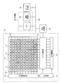
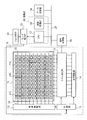
- FIG. 1 is a block diagram showing a configuration example of a solid-state image sensor according to the first embodiment of the present disclosure.
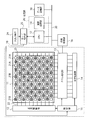
- the solid-state image sensor of FIG. 1 includes an image sensor 10, a signal processing unit 16, a CPU (Central Processing Unit) 17, a data storage unit 18, an arithmetic processing unit 19, and a bus 20.
- the image pickup device 10 includes a pixel array unit 11 having a plurality of pixels 21, a vertical drive unit 12, a column processing unit 13, a horizontal drive unit 14, and a control unit 15.
- the processing unit 26 is composed of the CPU 17 and the arithmetic processing unit 19.
- the solid-state image sensor shown in FIG. 1 is, for example, a CMOS (Complementary Metal Oxide Semiconductor) type solid-state image sensor, and can be used in various electronic devices.
- electronic devices include mobile devices having an imaging function such as smartphones, tablets or mobile phones, imaging devices such as digital still cameras and video cameras, surveillance cameras or in-vehicle cameras.
- the pixel array unit 11 and the logic circuit are arranged on the same support substrate and irradiated from the back surface of the substrate. It may be a back-illuminated type.
- the structure of the image pickup element 10 may be a laminated type in which the pixel array unit 11 and the logic circuit are separately manufactured and laminated. In this case, the laminated layers are electrically connected via a connecting portion such as a via. In addition to vias, it can also be connected by Cu-Cu bonding or bumps.
- the structure of the image sensor is as follows: pixel array unit 11, vertical drive unit 12, column processing unit 13, horizontal drive unit 14, control unit 15, signal processing unit 16, CPU 17, data storage unit 18, arithmetic processing unit 19, and bus.
- a laminated type including 20 may be used.
- the pixel array unit 11 includes a plurality of pixels 21 arranged in a two-dimensional shape (matrix shape). The area where the plurality of pixels 21 are arranged corresponds to the pixel area.
- the pixel 21 includes a photoelectric conversion unit including a photodiode (PD: Photodiode) and a plurality of pixel transistors.
- PD Photodiode
- a photodiode is an element that converts incident light into an electric signal (signal charge) by photoelectric conversion.
- the plurality of pixel transistors are, for example, MOS (Metal Oxide Semiconductor) transistors.
- the photoelectric conversion unit of the pixel 21 receives light through an optical lens (not shown) and generates an electric signal that changes logarithmically with respect to the amount of incident light as a pixel signal.
- the generated electric signal (pixel signal) is a voltage signal representing the output voltage of the pixel 21. Since the current flows exponentially with respect to the voltage generated by the photodiode in the pixel 21, the voltage and the current have a logarithmic relationship, and a logarithmic voltage signal is output.
- the pixel 21 that generates a voltage signal having a logarithmic characteristic as a pixel signal with respect to the amount of incident light is called a logarithmic pixel.
- the pixel 21 may be referred to as a logarithmic pixel 21.
- the logarithmic pixel 21 corresponds to an example of the first pixel, and the pixel signal read from the logarithmic pixel 21 corresponds to the first pixel signal read from the first pixel.
- a logarithmic pixel has a characteristic that it has a wide dynamic range, although it has more noise than a pixel having a linear characteristic (called a linear pixel) in which an output signal increases linearly with respect to the amount of light.
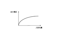
- FIG. 2 shows a graph schematically showing the relationship between the amount of incident light on a logarithmic pixel and the output voltage.
- the output voltage increases logarithmically as the amount of incident light increases.
- the relationship between i and v can be approximated by the following natural logarithm equation as an example.
- A is a predetermined coefficient.
- a is called the base and b is called the antilogarithm.
- a constant term may be included on the right side of the equation (1).
- FIG. 3 shows an example of the circuit configuration of the logarithmic pixel 21.
- the configuration of one logarithmic pixel 21 is shown, but the other logarithmic pixel 21 also has the same configuration.
- the logarithmic pixel 21 includes a photodiode 31 corresponding to a photoelectric conversion unit and a plurality of pixel transistors.
- the plurality of pixel transistors are an output transistor 32, an amplification transistor 33, a bias transistor 34, an amplification transistor 35, and a selection transistor 36.
- the output transistor 32, the amplification transistor 33, the amplification transistor 35, and the selection transistor 36 are composed of an N-type transistor as an example.
- the bias transistor 34 is composed of a P-type transistor as an example.
- the conductive type of these pixel transistors may be opposite to those illustrated here. In this case, it is necessary to change the logic of the control signal of these pixel transistors and the voltage of the power supply line.
- the drain terminal of the output transistor 32 is connected to the power supply voltage, and the source terminal is connected to the cathode terminal of the photodiode 31.
- the anode terminal of the photodiode 31 is connected to a reference voltage.
- the reference voltage is, for example, the ground voltage.
- the cathode terminal of the photodiode 31 is connected to the gate terminal of the amplification transistor 33.
- the connection node N1 of the photodiode 31 and the amplification transistor 33 is connected to the source terminal of the output transistor 32.
- the bias transistor 34 and the amplification transistor 33 are connected in series between the power supply voltage and the reference voltage. Further, the connection node N2 of the bias transistor 34 and the amplification transistor 33 is connected to the gate terminal of the output transistor 32 and the gate terminal of the amplification transistor 35. The output transistor 32 and the amplification transistor 33 are connected in a loop via the connection node N2 and the connection node N1.
- a bias voltage Vbias1 is applied to the gate terminal of the bias transistor 34.
- the drain terminal of the amplification transistor 35 is connected to the power supply voltage, and the source terminal is connected to the drain terminal of the selection transistor 36.
- the source terminal of the selection transistor 36 is connected to the vertical signal line 23.
- the gate terminal of the selection transistor 36 is connected to the pixel drive line 22, and the selection transistor 36 is controlled by the selection signal SEL supplied by the vertical drive unit 12.
- the photodiode 31 outputs a current i that changes linearly with respect to the amount of incident light.
- a voltage corresponding to this current i is applied to the gate terminal of the amplification transistor 33.
- the output transistor 32 and the amplification transistor 33 each operate as a source follower in the subthreshold region.
- the output transistor 32 and the amplification transistor 33 connected in a loop feed back the voltage of the connection node N1 to the gate terminal of the output transistor 32 via the amplification transistor 33.
- a voltage signal logarithmic of the current i is generated in the connection node N2, and the generated voltage signal is given to the amplification transistor 35 via the buffer circuit 40.
- This voltage signal is amplified by the amplification transistor 35.
- the amplified voltage signal is output to the vertical signal line 23 via the selection transistor 36. In this way, the voltage signal that changes logarithmically with respect to the amount of incident light is output as a pixel signal.
- the logarithmic pixel configuration shown in FIG. 3 is an example, and the logarithmic pixel configuration is not limited to the configuration shown in FIG. Any configuration may be used as long as it can detect a voltage signal that changes according to the logarithm of the photocurrent. Further, a circuit having a specific function may be added to the configuration of FIG. For example, a sensor circuit that detects a change in brightness may be connected to the connection node N2 in parallel with the amplification transistor 35.
- the vertical drive unit 12 of FIG. 1 sequentially selects the pixel drive lines 22 of the pixel array unit 11 in the vertical direction, and drives a plurality of pixels 21 commonly connected to the selected pixel drive lines 22.
- (Drive signal) is supplied.
- the vertical drive unit 12 sequentially selects the pixels 21 of the pixel array unit 11 in the vertical direction in line units, and supplies a drive signal such as a selection signal SEL or a reset signal RST described later to the pixel drive line 22 of the selected line. To do.
- the pixel signal generated in each pixel 21 is supplied to the column processing unit 13 via the vertical signal line 23.
- the vertical drive unit 12 is composed of a circuit such as a shift register.
- the column processing unit 13 performs signal processing of the signal output from the pixel 21 for one row for each pixel string.
- the column processing unit 13 includes a unit circuit corresponding to each pixel string.
- the unit circuit corresponding to each pixel sequence receives a signal output from the corresponding pixel of the pixels 21 of one row, and performs signal processing of the signal. Examples of signal processing include AD (Analog to Digital) conversion, and may further include noise removal and signal amplification before AD conversion.
- AD Analog to Digital
- the horizontal drive unit 14 sequentially outputs the horizontal scanning pulses to sequentially select the unit circuits in the column processing unit 13. As a result, pixel signals are sequentially output to the signal processing unit 16 from each of the unit circuits in the column processing unit 13.
- the horizontal drive unit 14 is composed of a circuit such as a shift register.
- the control unit 15 is a circuit that controls the operation of each part of the solid-state image sensor.
- the control unit 15 may use various signals such as a clock signal as a reference for the operation of the vertical drive unit 12, the column processing unit 13, the horizontal drive unit 14, etc. Generate a control signal.
- the control unit 15 outputs the generated signal to the vertical drive unit 12, the column processing unit 13, the horizontal drive unit 14, and the like.
- the signal processing unit 16 performs various signal processing on the pixel signal supplied from the column processing unit 13.
- the signal processing may only buffer the pixel signal.
- Other examples of signal processing include black level adjustment, column variation correction, or various digital signal processing.
- the signal processing unit 16 is composed of circuits such as a DSP (Digital Signal Processor), an ASIC (Application Specific Integrated Circuit), an FPGA (Field Programmable Gate Array), and a CPU.
- the signal processing unit 16 is connected to the bus 20.
- the CPU 17 is connected to the bus 20 and controls the signal processing unit 16, the data storage unit 18, and the arithmetic processing unit 19.
- the CPU 17 controls to write the pixel signal data processed by the signal processing unit 16 into the data storage unit 18 as pixel data.
- the data storage unit 18 internally stores the pixel data processed by the signal processing unit 16. By storing the pixel data corresponding to each pixel 21 in the data storage unit 18, the image data for one frame is stored in the data storage unit 18.
- the pixel data is a digital value having a predetermined bit length, and the bit length is determined according to the set resolution of AD conversion.
- image data is acquired at a fixed cycle and stored in the data storage unit 18.
- the data storage unit 18 is composed of an arbitrary volatile or non-volatile memory device such as a SRAM (Static Random Access Memory), a DRAM (Dynamic Random Access Memory), a NAND flash memory, or a magnetic resistance memory, as an example.
- the data storage unit 18 may be configured by a storage medium other than the memory device, such as a register or a digital circuit.
- the data storage unit 18 is connected to the bus 20.
- the arithmetic processing unit 19 receives the image data for one frame stored in the data storage unit 18 as input and performs the arithmetic processing of the neural network to perform image recognition of the image data. That is, the arithmetic processing unit 19 performs image recognition of an image based on the image signal read from each pixel 21.
- image recognition there is whether or not a predetermined object appears in the image data. For example, there is whether or not a person's face is shown.
- the type of object shown in the image data may be predicted from a plurality of candidates. For example, it may predict whether an object is a human, a non-human animal, or an object.
- the number of candidates is 3 in this example, but it may be 2 or 4 or more. Examples of image recognition may be other than these as long as they can be performed based on image data.
- the arithmetic processing unit 19 stores data representing the result of image recognition in the data storage unit 18.
- the data storage unit 18 stores data representing the result of image recognition calculated by the arithmetic processing unit 19.
- the arithmetic processing unit 19 is composed of circuits such as a DSP (Digital Signal Processor), an ASIC (Application Specific Integrated Circuit), an FPGA (Field Programmable Gate Array), or a CPU as an example.
- the arithmetic processing unit 19 may include an internal buffer for storing data.
- the internal buffer consists of any circuit such as a register, memory or digital circuit.
- the memory may be a volatile memory or a non-volatile memory.
- the CPU 17 may execute a part of the processing performed by the arithmetic processing unit 19.
- the data storage unit 18 stores the parameters of the neural network used by the arithmetic processing unit 19 for the arithmetic processing of the neural network.
- the parameter is a value obtained by converting the weighting coefficient representing the strength of the connection (link) between the nodes of the trained neural network into a logarithm having a base of 2.
- the converted weighting factor sometimes referred to as logarithmic weighting factor, or log 2 weighting factor.
- the logarithmic weighting factor is a logarithmic representation of the strength of the bond between a plurality of nodes.
- the logarithmic weighting coefficient is used instead of the learned weighting coefficient in the arithmetic processing of the neural network.
- the data storage unit 18 stores information in which an identifier representing a link between each node of the neural network and a logarithmic weighting coefficient are associated with each other as a form of storing the logarithmic weighting coefficient.
- This information may be, for example, a table or a function that returns a logarithmic weighting factor depending on a given identifier.
- All or part of the data described as being stored in the data storage unit 18 may be stored in the internal buffer of the arithmetic processing unit 19.
- the above parameters may be stored in the internal buffer of the arithmetic processing unit 19.
- the data storage unit 18 may store the learned weighting coefficient.
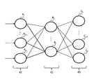
- FIG. 4 is a diagram schematically showing an example of a typical structure of a neural network.
- an example of a fully connected hierarchical neural network in which all nodes are interconnected between layers is shown as a neural network, but other types of neural networks such as a convolutional neural network or an interconnected neural network are shown. May be used.
- the neural network includes an input layer 41, an intermediate layer (hidden layer) 42, and an output layer 43.
- an intermediate layer 42 is shown here, a plurality of intermediate layers may exist.
- they are called the first intermediate layer, the second intermediate layer, ..., The final intermediate layer in order from the side closest to the input layer 41.
- the larger the number of intermediate layers the better the identification accuracy.
- the input layer 41 has a plurality of (q) input units A 1 to A q .
- the intermediate layer 42 has a plurality of (j) arithmetic units B 1 to B j .
- the output layer 43 has a plurality of (n) arithmetic units C 1 to C n .
- the input units A 1 to A q are referred to as input nodes A 1 to A q
- the arithmetic units B 1 to B j in the intermediate layer are referred to as intermediate nodes B 1 to B j
- the arithmetic units in the output layer are referred to.
- Each intermediate node of the intermediate layer 42 is bonded on all the links of the plurality of input nodes A 1 ⁇ A q of the input layer 41.
- a learned weighting factor is set for each link.
- Each output node of the output layer 43 is linked to all of the plurality of intermediate nodes B 1 to B j of the intermediate layer 42.
- a learned weighting factor is set for each link.
- Input data is given to the input nodes A 1 to A q . It is assumed that the input data is each pixel data of the image data. As an example, the number of input nodes is the same as the number of pixels for inputting image data, and the pixel data of each pixel is given to the input node.
- the product-sum operation (weighting total) of the input data and the weighting coefficient is performed.
- the result of the product-sum operation is used as the input variable of the activation function, and the activation function is calculated.
- Each intermediate node outputs the output value of the activation function to the output nodes C 1 to C n .
- the weighting coefficients between the intermediate nodes B 1 and the input nodes A 1 to A q are set to w 1 to w q , and the data input from the input nodes A 1 to A q to the intermediate nodes B 1 is d 1 Let it be ⁇ d q .
- the product-sum operation value (X B1 ) at the intermediate node B 1 and the output value (Y B1 ) of the activation function are expressed by the following equations.
- the function f represents an activation function.
- ⁇ represents a product-sum operation (weighted total) of the weighting coefficients w 1 to w q and the input data d 1 to d q .
- ⁇ represents a product-sum operation (weighted total) of the weighting coefficients w 1 to w q and the input data d 1 to d q .
- an operation example of the intermediate node B 1 is shown, but the same operation is performed on the intermediate nodes B 2 to B j .
- the output values of the intermediate nodes B 1 to B j are the data input to the output nodes C 1 to C m .
- any non-linear function such as a ReLU function or a step function is used.
- the use of linear functions is not excluded.
- the ReLU function is a function that outputs 0 if the input variable is 0 or less, and outputs the value of the input variable as it is if it exceeds 0. Assuming that the ReLU function is ReLu (x) and the input variable is x, ReLu (x) is defined as follows.
- the step function is a function that outputs 0 if the input variable is 0 or less, and outputs 1 if the input variable exceeds 0. Assuming that the step function is Step (x) and the input variable is x, Step (x) is defined as follows.
- each output node is the same as the operation of the intermediate node. More particularly, each output node to the input data from the intermediate node B 1 ⁇ B j, multiplied by the weighting factor for the intermediate nodes B 1 ⁇ B j, summing the multiplication results. That is, the product-sum operation (weighting total) of the input data and the weighting coefficient is performed. The result of the product-sum operation is used as the input variable of the activation function, and the activation function is calculated. The output value of the activation function in each output node becomes the output of each output node.
- the activation function of each output node in the output layer is the same, but the activation function may differ depending on the output node. Further, the activation function of the output layer may be different from or the same as the activation function of the intermediate layer.
- the arithmetic processing unit 19 performs determination processing based on the output value of each output node, and outputs the result of the determination processing as the result of image recognition.
- a class is assigned to each output node, and the class of the output node that outputs the largest output value is used as the identification result. For example, suppose that there are two output nodes, and the first class assigned to one output node (first output node) is a class indicating that a human face is shown in the image. Then, it is assumed that the second class assigned to the other output node (second output node) is a class indicating that a human face is not shown in the image. In this case, if the output value of the first output node is larger than the output value of the second output node, a signal indicating the first class is output. That is, it is determined that a human face is reflected in the image data given as input to the neural network. If the output value of the second output node is larger than the output value of the first output node, a signal indicating the second class is output. That is, it is determined that the human face is not shown in the image data given as the input to the neural network.
- the judgment process based on the output value of each output node described above is an example, and other judgment processes are also possible.
- the output value of each output node is compared with the threshold value, and when the ratio of the number of output nodes for which an output value equal to or higher than the threshold value is obtained is equal to or more than a certain value, the first identification result is determined (for example, a person in the image). Judged that the face is visible). If the ratio is less than a certain value, a second identification result is determined (for example, it is determined that the image does not show a human face).
- the largest output value among the output values of the output node is specified, and if the specified output value is equal to or more than a certain value, the first identification result is determined, and if it is less than a certain value, the second identification result is determined. You may decide.
- the threshold value is stored in advance in the internal buffer of the data storage unit 18 or the arithmetic processing unit 19.
- the determination method based on the output value of each output node can be arbitrarily defined according to the configuration of the neural network, the learning method, and the like.
- each intermediate node of the first stage of the intermediate layer is bonded at all the links of the input nodes A 1 ⁇ A q, the weighting factor is set for each link.
- each intermediate node of the intermediate layer in the subsequent stage is connected to all the intermediate nodes in the intermediate layer in the previous stage by a link, and a weighting coefficient is set for each link.
- Each output node of the output layer 43 is linked to all the intermediate nodes of the intermediate layer of the final stage, and a weighting coefficient is set for each link.
- the output values of all the intermediate nodes of the intermediate layer of the previous stage are input data.
- the calculation of each intermediate node of the intermediate layer after the second stage is the same as that of the intermediate layer 42 described above.
- a plurality of image data whose identification results (correct answers) are known in advance are prepared as learning data, and when the image data is input to the input layer, the identification results (correct identification results) can be obtained. This is done by adjusting the weighting coefficient between the nodes.
- the identification result known in advance is called a teacher signal.
- Such adjustment of the weighting coefficient may be performed by using a method such as a back propagation method (backpropagation method).
- the backpropagation method is a method of adjusting the weighting coefficient in order from the output layer side so that the deviation between the output of the neural network and the teacher signal becomes small.
- FIG. 4 is used in the description of a general neural network, the structure of the neural network is universally shown, and the description of the neural network according to the present embodiment is also based on FIG.
- the neural network according to the present embodiment corresponds to the first neural network as an example, and each node in the first neural network corresponds to the first node as an example.
- the arithmetic processing unit 19 converts the pixel data into data and uses this as the input data (first input data). More specifically, the data (log 2 i) obtained by converting the current value i related to the above equation (1) into the logarithm of the base 2 with respect to the value (voltage value) indicated by the pixel data of each pixel 21. Use.
- the converted data is called logarithmic pixel data.
- the logarithmic pixel data (log 2 i) is obtained by converting the above equation (1) as in equation (5-1) using the logarithms change formula, and then as in equation (5-2). ) Can be derived.
- log 2 i can be calculated by multiplying the pixel data value (v) by A'. Since A'is a fixed value, this operation is simple and can be realized with a small amount of calculation or a small circuit. That is, the circuit for converting (log 2 transform) pixel data in the bottom 2 of the logarithm (log 2 conversion circuit) is not required.
- log 2 e is an example of a logarithm including a predetermined value (here, the number of Napiers) as an antilogarithm.
- the logarithm weight coefficient obtained by converting the learned weight coefficient into the logarithm of the base 2 is used as the weight coefficient between each node. Between each node is between an input node and an intermediate node, and between an intermediate node and an output node. When there are a plurality of intermediate layers, the intermediate nodes between different intermediate layers are also included. As described above, the arithmetic processing of the neural network according to the present embodiment is performed based on the logarithmic pixel data given to each input node and the logarithmic weighting coefficient set between each node.
- log 2 of the total value of the true numbers of the addition results (logarithms) for each input node is calculated.
- Calculation of log 2 which is the sum of the true numbers of a plurality of logarithms is called "log 2 addition”. Also called a value calculated by log 2 addition and log 2 added value.
- log 2 addition For example, if the addition result for each input node is log 2 (i 1 * w 1 ), ..., log 2 (i q-1 * w q-1 ), log 2 (i q * w q ), these The log 2 addition value of log 2 is log 2 (i 1 * w 1 +, ..., + I q-1 * w q-1 + i q * w q ). Log 2 addition can be realized with a small amount of calculation or a small circuit.
- the output value of the activation function is calculated using the calculated log 2 addition value as the input variable of the activation function.
- an example intermediate node B 1 in FIG. 4 a specific example.
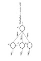
- Figure 5 is a diagram for explaining an example of calculation processing of the intermediate nodes B 1.
- the logarithmic weighting coefficient set between the intermediate node B 1 and the input nodes A 1 to A q be log 2 w 1 to log 2 w q .
- the arithmetic value at intermediate nodes B 1 (X 'B1), the output value of the activation function (Y' B1) is expressed by the following equation.
- the ReLU function is used as the activation function.
- the calculated value (log 2 addition value) of the node in the neural network according to the present embodiment is the node in the general neural network.
- the calculated value (product-sum calculated value) of the above is the node in the general neural network.
- the arithmetic processing of the output nodes C 1 to C n is the same as that of the intermediate node except that the data input from the previous layer is the output value of each intermediate node. Since the output value of the intermediate node is the logarithm of the base 2, the output node can also perform the log 2 addition operation in the same manner as the intermediate node.
- the output node can perform the same operation as the intermediate node.
- Arithmetic processing unit 19 performs a determination process based on the output value of the output nodes C 1 ⁇ C n (bottom 2 logarithm), the result of the determination processing, and outputs the result of the image recognition.
- the details of the determination process are the same as the determination process of the general neural network described above.
- a class is assigned to each output node, and the class of the output node that outputs the largest output value is used as the result of image recognition.
- a method of comparing the output value of each output node described above with the threshold value is also possible.
- a value obtained by converting the threshold value into the logarithm of the base 2 (logarithmic threshold value) may be used. This makes it possible to compare logarithms with each other.
- the logarithmic threshold is stored in advance in the internal buffer of the data storage unit 18 or the arithmetic processing unit 19.
- the multiplication circuit becomes unnecessary and the circuit scale is also reduced. Moreover, since the amount of calculation is reduced, the power consumption is also reduced.
- log 2 addition circuit for efficiently performing the log 2 addition calculation.
- log 2 addition of the log 2 (i 1 * w 1) and log 2 (i 2 * w 2 ) can be approximated by the following equation (see Non-Patent Document 1).
- the first term of equation (7) means the maximum value of log 2 (i 1 * w 1 ) and log 2 (i 2 * w 2 ).
- the second term is a power of 2 by the minus of the absolute value of the difference between log 2 (i 1 * w 1 ) and log 2 (i 2 * w 2 ).
- the second term is equivalent to bit-shifting 1 to the right (in the direction of the smaller digit) by the absolute value of the difference. That is, the bit string in which the decimal number 1 is represented by bits is bit-shifted to the right by
- the bit shift is done to the right because the exponent of power 2 is a negative value. For example, when 1 is expressed as 00001000 and the absolute value of the above difference is 3, it becomes 00000001 by performing a 3-bit shift. Note that the bit notation rules may be set arbitrarily, and this example is only an example.
- FIG. 6 is a block diagram of an example of the log 2 addition circuit.
- the log 2 addition circuit is included in the arithmetic processing unit 19.
- the plurality of input nodes A 1 ⁇ A q log are respectively calculated by summing the logarithmic pixel data and logarithmic weight to 2 (i n * w n) (n is an integer of 1 ⁇ q), cumulative addition
- An example of the circuit configuration is shown.
- the circuit of FIG. 6 includes a selector 51, an adder 52, a subtractor 53, an absolute value calculator 54, a power calculator 55, and a flip-flop circuit 56.
- the selector 51 has a first input terminal and a second input terminal.
- the first input terminal newly calculated subject to log 2 (i n * w n ) is input, representative of this data P n.
- the value log 2 (i 1 * w 1 + ... + in -1 * w n-1 ) accumulated up to the previous time is input to the second input terminal, and this is represented as data S n-1 .
- the data P n and the data S n-1 are also input to the subtractor 53.
- Subtractor 53 subtracts the S n-1 from P n.
- the output of the subtractor 53 is connected to the control terminal of the selector 51.
- the subtractor 53 outputs a signal indicating the sign of the subtraction result to the control terminal of the selector 51, and outputs a signal indicating the subtraction result to the absolute value calculator 54.
- the selector 51 outputs data P n when the subtraction result indicates positive, and outputs data S n-1 when the subtraction result indicates negative. That is, the larger of the data P n and Sn-1 is output.
- the subtractor 53 may be configured to subtract P n from Sn -1 . In this case, the selector 51 outputs data Sn-1 when the subtraction result is positive, and data when the subtraction result is negative. P n may be output.
- the absolute value calculator 54 is connected to the output of the subtractor 53, and calculates the absolute value
- the power calculator 55 is connected to the output of the absolute value calculator 54 and calculates the power of 2 ⁇
- the adder 52 is connected to the output of the selector 51 and the output of the exponentiation calculator 55, and adds the value selected by the selector 51 and the value after being bit-shifted by the exponentiation calculator 55.
- the flip-flop circuit 56 is connected to the output of the adder 52, and stores the addition result (approximate value of log 2 (i 1 * w 1 + i 2 * w 2 )) of the adder 52 internally.
- Flip-flop circuit 56 is connected to the second input terminal of the selector 51, and feeds back this value as data S 2 to the second input terminal and a subtracter 53.
- Log 2 (i 3 * w 3 ) to be calculated next is input as data P 3 to the first input terminal of the selector 51.
- log 2 (i n * w n) are cumulatively log 2 addition, and finally, log 2 (i 1 * w 1 + ⁇ + i q * w q ) Is output from the flip-flop circuit 56 that operates on the clock CLK.
- the output value of the flip-flop circuit 56 becomes an input variable of the activation function.
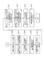
- FIG. 7 is a flowchart of an example of the operation of the solid-state image sensor according to the present embodiment.
- the predetermined event may be any event that occurs or is detected by the device equipped with this device.
- a user who operates a device equipped with this device may have performed a predetermined operation, a predetermined time has come, or a vibration exceeding a certain value has been detected, but the present invention is not limited to these.
- this trigger one frame is imaged by the pixel array unit 11 under the control of the control unit 15.
- a pixel signal (voltage signal) that changes logarithmically with respect to the amount of incident light is generated by photoelectric conversion in each pixel 21, and the generated pixel signal is read out and sent to the signal processing unit 16 (S101).
- These pixel signals are AD-converted by the column processing unit 13 (S102), and a set of pixel data of each pixel obtained by the AD conversion is stored in the data storage unit 18 as image data (S103).
- the arithmetic processing unit 19 reads the image data from the data storage unit 18 and performs data conversion on each pixel data included in the image data (S104).
- the data conversion operation is, for example, multiplying log 2 e / A (see equations (5-1) and (5-2)). That is, the logarithm including the Napier number (predetermined value) in the antilogarithm is multiplied by the value of the pixel data.
- the data (log 2 i) obtained by converting the value of the pixel data into the logarithm of the base 2 is calculated as the logarithm pixel data (S104).
- the arithmetic processing unit 19 reads from the data storage unit 18 a logarithmic weighting coefficient (log 2 weighting coefficient), which is the logarithm of the weighting coefficient set between each node in the neural network (S105). Between each node is between an input node and an intermediate node, and between an intermediate node and an output node. When there are a plurality of intermediate layers, the intermediate nodes between different intermediate layers are also included.
- the logarithmic weighting coefficient may be stored in advance in the internal buffer of the arithmetic processing unit 19 instead of the data storage unit 18.
- a neural network having one intermediate layer see FIG. 4 is assumed, but a plurality of neural networks is also possible. In this case, in the intermediate layer of the second and subsequent stages, the input data is changed not from the input node but from the intermediate node of the intermediate layer of the previous stage, and the processing content is the same as that of the intermediate layer of the first stage. ..
- the arithmetic processing unit 19 allocates the logarithmic pixel data of each pixel 21 as input data to each input node of the neural network (S106). Which pixel 21 is associated with which input node is determined in advance at the time of learning.
- the one-to-one correspondence between the pixel 21 and the input node is only an example, and the input data to be assigned to each input node may be generated by another method.
- a pixel group is composed of a predetermined number of pixels 21, and each pixel group is associated with each input node.
- the representative value of logarithmic pixel data is determined by the pixel group, and the representative value is assigned to the input node as input data.
- the representative value may be any statistical value such as an average value, a maximum value or a minimum value. It is also possible to assign the pixel data of the difference between the logarithmic pixel data read this time and the logarithmic pixel data read last time to the input node as input data.
- the arithmetic processing unit 19 performs arithmetic on each intermediate node based on the input data assigned to each input node and the logarithmic weighting coefficient set between each intermediate node and each input node (S107). That is, the logarithmic weighting coefficient and the input data are added to each input node, and all the addition results are added by log 2 .
- the arithmetic processing unit 19 calculates the activation function using the log 2 addition value as an input variable (S107). Let the output value of the activation function be the output value of each intermediate node. The output value of each intermediate node is the data input to the output layer of the next stage.
- each output node is performed based on the output value of each intermediate node and the logarithmic weighting coefficient set between each intermediate node and each output node (S108). That is, for each intermediate node, the logarithmic weighting coefficient and the input data are added, and all the addition results are log 2 added.
- the arithmetic processing unit 19 calculates the activation function using the log 2 addition value as an input variable (S108). The output value of the activation function becomes the output value of the output node.
- the arithmetic processing unit 19 performs determination processing based on the output value of each output node (S109). As an example, the output node for which the largest output value is calculated is specified, and the class assigned to the specified output node is acquired as the result of image recognition. As described above, various algorithms such as processing using a threshold value can be used for judgment recognition. Any algorithm may be used.
- the arithmetic processing unit 19 stores data indicating the result of image recognition in the data storage unit 18.
- the CPU 17 reads data indicating the result of image recognition from the data storage unit 18 and outputs it to the outside (S110). For example, it outputs to an application program running on the device on which this device is installed. In this case, the application program performs processing according to the result indicated by the data. Further, data indicating the result of image recognition may be displayed on the screen of the display device included in the device on which the present device is mounted.
- step order is an example, and the order of some steps may be changed.
- step S104 and step S105 may be reversed.
- the logarithmic input data of the base 2 is generated by data conversion of the data of the pixel signal (voltage signal) read from the logarithmic pixel. Therefore, since a circuit that converts the base 2 to the logarithm (log 2 conversion circuit) is not required, the circuit scale can be reduced and the power consumption can be reduced.
- the data of the pixel signal read from the logarithmic pixel since the data of the pixel signal read from the logarithmic pixel is used, image recognition that makes the best use of the characteristics of the high dynamic range of the logarithmic pixel becomes possible.
- the data of the pixel signal read from the linear pixel is converted into the logarithm of the base 2 by the log 2 conversion circuit, but in this case, the dynamic range of the converted data is rate-determined by the dynamic range of the linear pixel. Therefore, the effect of high dynamic range cannot be obtained.
- the present embodiment since reading from logarithmic pixels is performed, the effect of a high dynamic range can be obtained.
- the logarithmic pixel data obtained by converting the pixel data (the logarithm of the base 2) and the logarithm weighting coefficient (the logarithm of the base 2) are used, the calculation at each node can be performed by addition. .. Therefore, multiplication (multiplication of the weighting coefficient and the input data) at each node becomes unnecessary. Therefore, the amount of calculation can be reduced and the power consumption can be reduced. Moreover, since the multiplication circuit is not required, the circuit scale can be reduced.
- the logarithm of the base 2 is used, but the base of the logarithm does not necessarily have to be 2. Even if the base is not 2, it can be expected that the amount of calculation can be reduced by performing the addition operation in the logarithmic region at each node.
- Modification 2 The configuration of the logarithmic pixel shown in the first embodiment (FIG. 3) is an example, and various modifications are possible. A modified example of the logarithmic pixel will be described with reference to FIG.
- FIG. 8 is a circuit diagram showing a modified example of logarithmic pixels.
- a reset transistor 37, a buffer transistor 38, and a bias transistor 39 are added to the logarithmic pixels of FIG. 3 as pixel transistors.
- the buffer transistor 38 and the bias transistor 39 form a buffer circuit 40.
- the reset transistor 37 is composed of an N-type transistor as an example.
- the buffer transistor 38 and the bias transistor 39 are composed of a P-type transistor as an example.
- connection node N2 is connected to the gate terminal of the output transistor 32 and the gate terminal of the buffer transistor 38.
- the voltage signal generated in the connection node N2 is given to the amplification transistor 35 via the buffer circuit 40. This voltage signal is amplified by the amplification transistor 35.
- a bias transistor 39 and a buffer transistor 38 are connected in series between the power supply voltage and the reference voltage.
- a bias voltage Vbias2 is applied to the gate terminal of the bias transistor 39.
- the connection node between the bias transistor 39 and the buffer transistor 38, that is, the output terminal of the buffer circuit 40 is connected to the source terminal of the reset transistor 37 and the gate terminal of the amplification transistor 35.
- the drain terminal of the reset transistor 37 is connected to the power supply voltage.
- the gate terminal of the reset transistor 37 is connected to the pixel drive line 22.
- the reset transistor 37 is controlled by the reset signal RST supplied by the vertical drive unit 12.
- the signal processing unit 16 or the column processing unit 13 performs CDS (Correlated Double Sampling) processing in which the reset transistor 37 is turned on, a signal that does not include a pixel signal is detected, and the detected signal is removed (subtracted) from the pixel signal. Do. As a result, fixed pattern noise caused by variations in pixel transistors and the like is removed.
- the pixel signal may be read before or after the signal that does not include the pixel signal is read.
- the signal obtained by the CDS processing can be used as a pixel signal read from logarithmic pixels.
- the buffer circuit 40 functions to reduce the influence of the potential of logarithmic pixels (potential of node N2) at the time of reset. As a result, the potential of the logarithmic pixel can be made an output that always depends on the amount of light. It is also possible not to perform the CDS processing while using the circuit configuration of FIG.
- the fixed pattern noise included in the pixel signal can be removed by performing the CDS processing.
- FIG. 9 is a circuit diagram showing another modification of the logarithmic pixel.
- the event detection unit 80 is added to the circuit configuration of FIG.
- the pixel circuit to which the event detection unit 80 is added may be called a DVS (Dynamic Vision Sensor) circuit.
- the configuration of the buffer circuit 40 is schematically shown by symbols here.
- the event detection unit 80 detects the presence or absence of an event depending on whether or not the amount of change in the photocurrent from the photodiode 31 exceeds a predetermined threshold value. Examples of events include on-events where the amount of change exceeds the upper threshold, events where the amount of change falls below the lower threshold, or both.
- Detection of on-event or off-event corresponds, for example, to detecting a change in contrast (for example, detecting an object).
- the event detection unit 80 outputs a detection signal or a non-detection signal to the control unit 15 depending on whether or not an event is detected.
- the event detection unit 80 includes a subtractor 81 and a quantizer 82.
- a subtractor 81 is connected to the output terminal of the buffer circuit 40.
- a quantizer 82 is connected to the output terminal of the subtractor 81. It is also possible to add the event detection unit 80 to the circuit configuration shown in FIG.
- the subtractor 81 lowers the level of the voltage signal from the buffer circuit 40 according to the drive signal from the vertical drive unit 12.
- the subtractor 81 supplies the lowered voltage signal to the quantizer 82.
- the quantizer 82 quantizes the voltage signal from the subtractor 81 into a digital signal.
- the quantizer 82 compares the quantized signal with the threshold voltage Vth, and generates a signal (detection signal or non-detection signal) indicating the comparison result. As an example, if the threshold voltage Vth is the upper limit threshold value and the quantized signal is larger than the upper limit threshold value, a detection signal is generated. If the quantized signal is below the upper threshold, a non-detection signal is generated.
- the quantizer 82 outputs the generated detection signal or non-detection signal to the control unit 15. Similarly, when the threshold voltage Vth is the lower limit threshold value, a detection signal or a non-detection signal can be generated.
- the control unit 15 determines to read the pixel signal from the logarithmic pixel 21, and controls the vertical drive unit 12 to read the pixel signal from the logarithmic pixel 21.
- the control unit 15 determines not to read the pixel signal from the logarithmic pixel 21.
- the quantizer 82 can be configured to omit the output of the non-detection signal to the control unit 15 when the event is not detected.
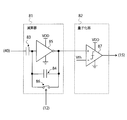
- FIG. 10 is a circuit diagram showing a configuration example of the subtractor 81 and the quantizer 82.
- the subtractor 81 includes a capacitor 83, a capacitor 84, an inverter 85, and a switch 86.
- the quantizer 82 includes a comparator 87.
- One end of the capacitor 83 is connected to the output terminal of the buffer circuit 40, and the other end is connected to the input terminal of the inverter 85.
- the capacitor 84 is connected in parallel with the inverter 85.
- the switch 86 connects both ends of the capacitor 84. The switch 86 opens and closes according to a drive signal from the vertical drive unit 12.
- the inverter 85 inverts the voltage signal input via the capacitor 83.
- the inverter 85 outputs the inverted signal to the non-inverting input terminal (+) of the comparator 87.
- the charge Q2 stored in the capacitor 84 is expressed by the following equation, where the output voltage is Vout.
- Q2 -C2 x Vout ... (8-3)
- Equation (8-5) represents the subtraction operation of the voltage signal, and the gain of the subtraction result is C1 / C2. Since it is usually desired to maximize the gain, it is preferable to design C1 to be large and C2 to be small. On the other hand, if C2 is too small, kTC noise may increase and noise characteristics may deteriorate. Therefore, the capacity reduction of C2 is limited to a range in which noise can be tolerated.
- the comparator 87 compares the voltage signal from the subtractor 81 with the threshold voltage Vth applied to the inverting input terminal ( ⁇ ). The comparator 87 outputs a detection signal or a non-detection signal depending on the comparison result.
- a logarithmic pixel and a linear pixel are used as the pixels to be arranged in the pixel array unit 11. Then, the pixel for reading the pixel signal is selected between the logarithmic pixel and the linear pixel according to the instruction data given from the outside.
- the subsequent processing is the same as that of the first embodiment.
- the subsequent processing is the same as the arithmetic processing of a general neural network.
- each node (intermediate node and output node) performs a product-sum operation based on the pixel data of each pixel and a weighting coefficient, and calculates an activation function using the result of the product-sum operation as an input variable.
- the present embodiment will be described in detail.
- FIG. 11 is a block diagram showing a configuration example of the solid-state image sensor according to the second embodiment of the present disclosure.
- An input / output terminal 24 and a mode indicator 25 are added to the solid-state image sensor of FIG.
- Elements having the same names as those in FIG. 1 are designated by the same reference numerals, and detailed description thereof will be omitted as appropriate except for extended or modified processing.
- the pixel array unit 11 includes two types of pixels, a logarithmic pixel 21A and a linear pixel 21B.
- the linear pixel 21B corresponds to an example of a second pixel which is a different type of pixel from the logarithmic pixel 21A.
- the pixel signal read from the linear pixel 21B corresponds to the second pixel signal read from the second pixel.
- the logarithmic pixels 21A and the linear pixels 21B are alternately arranged in the horizontal and vertical directions (arranged in a staggered pattern).
- the method of arrangement is not limited to this, and any method may be used.
- three pixels in the pixel block may be logarithmic pixels, and the remaining one may be a linear pixel.
- the pixel type may be the same for each column, and different types of pixel columns may be arranged alternately in the row direction (horizontal direction).
- the linear pixel generates an electric signal that changes linearly with respect to the incident light as a pixel signal. That is, the linear pixel produces an output signal that increases linearly with respect to the amount of light.
- Linear pixels have a narrow dynamic range as compared with logarithmic pixels, but have low noise characteristics.
- FIG. 12 shows a graph schematically showing the relationship between the amount of light incident on a linear pixel and the output voltage.
- the output voltage increases linearly (for example, proportionally) as the amount of incident light increases.
- FIG. 13 shows an example of the circuit configuration of the linear pixel 21B.
- the configuration of one linear pixel 21B is shown, but the other linear pixels 21B also have the same configuration.
- the linear pixel 21B includes a photodiode 61 corresponding to a photoelectric conversion unit and a plurality of pixel transistors.
- the plurality of pixel transistors are a transfer transistor 62, an amplification transistor 63, a selection transistor 64, and a reset transistor 65.
- These pixel transistors are MOS (Metal Oxide Semiconductor) transistors, and are composed of N-type transistors as an example. However, these transistors may be composed of P-type transistors. In this case, it is necessary to change the logic of the control signal of these pixel transistors and the voltage of the power supply line.
- the photodiode 61 is an element that converts incident light into an electric signal (signal charge) proportional to the amount of light by photoelectric conversion and stores it.
- the anode terminal of the photodiode 61 is connected to the reference voltage, and the cathode terminal is connected to the source terminal of the transfer transistor 62.
- the transfer transistor 62 is connected between the cathode terminal of the photodiode 61 and the FD node 66.
- the gate terminal of the transfer transistor 62 is connected to the vertical drive unit 12.
- the transfer transistor 62 is controlled by the transfer signal TRG from the vertical drive unit 12. When the transfer transistor 62 is turned on, the signal charge stored in the photodiode 61 is transferred to the FD node 66.
- the FD node 66 is a floating diffusion region connected between the drain terminal of the transfer transistor 62 and the gate terminal of the amplification transistor 63. As a result, the FD node 66 can accumulate the signal charge transferred from the photodiode 61.
- the FD node 66 is also connected to the source terminal of the reset transistor 65.
- the amplification transistor 63 is connected between the power supply voltage and the selection transistor 64.
- the gate terminal of the amplification transistor 63 is connected to the FD node 66.
- the amplification transistor 63 is in a conductive state according to the signal charge accumulated in the FD node 66.
- the selection transistor 64 is connected between the amplification transistor 63 and the vertical signal line 23.
- the gate terminal of the selection transistor 64 is connected to the vertical drive unit 12.
- the selection transistor 64 is controlled by the selection signal SEL from the vertical drive unit 12.
- the selection transistor 64 connects or disconnects the linear pixel 21B to or disconnects the vertical signal line 23.
- the vertical signal line 23 is set to a voltage corresponding to the signal level of the gate voltage of the amplification transistor 63.
- the reset transistor 65 is connected between the power supply voltage and the FD node 66.
- the gate terminal of the reset transistor 65 is connected to the vertical drive unit 12.
- the reset transistor 65 is controlled by the reset signal RST from the vertical drive unit 12. When the reset transistor 65 is turned on, the signal charge accumulated in the FD node 66 is discharged to the power supply voltage. As a result, the FD node 66 of the linear pixel 21B is reset.
- a voltage signal proportional to the amount of incident light is output as a pixel signal.
- the configuration of the linear pixel shown in FIG. 13 is an example, and the configuration of the linear pixel is not limited to the configuration of FIG. Any configuration may be used as long as a voltage signal proportional to the amount of light (charge) can be detected.
- the input / output terminal 24 is a terminal for transmitting / receiving a signal to / from an external device.
- the input / output terminal 24 transmits / receives signals to / from an external device by an arbitrary communication method such as serial communication.
- the external device may be a device in which the internal setting of the device equipped with the solid-state image sensor is performed from the outside of the device, or an operating means (for example, a button or the like) for the user to perform various settings.
- the mode instruction unit 25 receives the mode data instructing the mode of the pixel reading process via the input / output terminal 24.
- the pixel read mode includes a logarithmic read mode and a linear read mode.
- the logarithmic read mode performs a first read process for reading from logarithmic pixels.
- the linear read mode performs a second read process for reading from linear pixels.
- the mode data indicates one of these modes.
- the mode indicator 25 is configured by a storage element such as a register as an example. It is also possible to configure the CPU 17 to provide the mode data to the mode indicator 25.
- the control unit 15 reads the mode data from the mode indicator unit 25, and when the mode data indicates the logarithmic read mode, controls each unit so as to read the pixel signal from each logarithmic pixel 21A in the pixel array unit 11.
- the control unit 15 controls each unit so as to read the pixel signal from each linear pixel 21B in the pixel array unit 11. That is, the control unit 15 selectively executes the process of reading the pixel signal from each logarithmic pixel 21A and the process of reading the pixel signal from each linear pixel 21B.
- the column processing unit 13 performs signal processing of the signal output from the pixels 21 for one row for each pixel string.
- Examples of signal processing include AD conversion and may further include at least one of signal noise removal and signal amplification before AD conversion.
- the data storage unit 18 stores the parameters of the neural network used by the arithmetic processing unit 19 in the arithmetic processing of the neural network for each of the logarithmic read mode and the linear read mode.
- the neural networks in the logarithmic read mode and the linear read mode are different from each other, and learning is also performed separately.
- the data storage unit 18 converts the weighting coefficient representing the strength of the connection between the nodes into a logarithm having a base of 2, as in the first embodiment. (Logarithmic weight coefficient) is stored.
- the logarithmic weighting coefficient may be stored in the internal buffer of the arithmetic processing unit 19 instead of the data storage unit 18.
- the neural network for the logarithmic read mode corresponds to the first neural network as an example, and each node in the first neural network corresponds to the first node as an example.
- the data storage unit 18 stores a weighting coefficient representing the strength of the connection between each node as a parameter of the neural network for the linear read mode.
- the weighting coefficient may be stored in the internal buffer of the arithmetic processing unit 19 instead of the data storage unit 18.
- the neural network for the linear read mode corresponds to the second neural network as an example, and each node in the second neural network corresponds to the first node as an example.
- the CPU 17 reads the mode data from the mode indicating unit 25, and when the mode data indicates the logarithmic reading mode, controls the arithmetic processing unit 19 as in the first embodiment. That is, the arithmetic processing unit 19 converts the pixel data of each pixel into logarithmic pixel data (see equation (5-2)), and uses the logarithmic pixel data and the logarithmic weight coefficient between each node to form a neural network. Perform arithmetic processing. In each intermediate node and each output node, as described in the description of the first embodiment, the data input from the previous layer and the logarithmic weighting coefficient are added, and the addition result is added by log2 (formula (formula (formula)). See 6-1)). The output value of the activation function is calculated using the result of log2 addition as the input variable of the activation function (see equation (6-2)).
- the CPU 17 controls the arithmetic processing unit 19 so as to perform the same arithmetic as the general neural network described in the description of the first embodiment. That is, the arithmetic processing unit 19 uses the pixel data of each pixel as the input data (second input data) of the neural network, and performs arithmetic processing of the neural network using the input data and the weighting coefficient between each node. ..
- the data input from the previous layer is multiplied by the weighting coefficient (see equation (2-1)), and the multiplication results are added. That is, the product-sum calculation of the input data and the weighting coefficient is performed.
- the output value of the activation function is calculated using the result of the product-sum operation as the input variable of the activation function (see equation (2-2)).
- the arithmetic processing unit 19 includes both a circuit that performs the arithmetic processing of the neural network for the logarithmic read mode and a circuit that performs the arithmetic processing of the neural network for the linear read mode.
- the neural networks of both modes were learned separately, but it is not limited to this.
- a neural network learned in common may be used.
- the logarithmic pixel data and the logarithmic weighting coefficient are used in the logarithmic reading mode, and the pixel data and the weighting coefficient are used in the linear reading mode.
- the operations at each intermediate node and each output node are also different in each mode as described above.
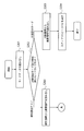
- FIG. 14 is a flowchart of an example of the operation of the solid-state image sensor according to the present embodiment.
- the control unit 15 reads the mode data from the mode indicator unit 25 (S201). It is confirmed whether the mode data indicates the logarithmic read mode or the linear read mode (S202). When the logarithmic read mode is instructed, the control unit 15 controls each unit so as to read a pixel signal from each logarithmic pixel 21A of the pixel array unit 11 (S203). The subsequent processing is the same as in steps S102 to S110 of FIG. 7 (S204).
- control unit 15 controls each unit so as to read a pixel signal from each linear pixel 21B of the pixel array unit 11 (S205). Subsequent processing is shown in FIG.
- FIG. 15 is a flowchart of an example of the operation following step S205 of FIG. The description of the step processing similar to the flowchart of FIG. 7 will be omitted as appropriate.
- the pixel signal read from each linear pixel 21B is AD-converted by the column processing unit 13 (S206), and the set of pixel data of each pixel obtained by the AD conversion is stored in the data storage unit 18 as image data ( S207).
- the arithmetic processing unit 19 reads the image data from the data storage unit 18 (S208), and reads the weighting coefficient between each node in the neural network for the linear read mode from the data storage unit 18 (S209).
- the arithmetic processing unit 19 allocates the pixel data of each pixel 21 as input data to each input node of the neural network (S210). Which pixel 21 is associated with which input node is determined in advance at the time of learning.
- the one-to-one correspondence between the pixel 21 and the input node is only an example, and the input data to be assigned to each input node may be generated by another method.
- the arithmetic processing unit 19 performs arithmetic of each intermediate node based on the input data assigned to each input node and the weighting coefficient between each intermediate node and each input node (S211). That is, the weighting coefficient for each input node is multiplied by the input data, and the sum of the multiplication results is calculated. That is, the product-sum operation of the weighting coefficient and the input data is performed.
- the arithmetic processing unit 19 calculates the activation function using the result of the product-sum operation as an input variable (S211). Let the output value of the activation function be the output value of each intermediate node. The output value of each intermediate node is the data input to the output layer of the next stage.
- Calculation of each output node is performed based on the output value of each intermediate node and the weighting coefficient between each intermediate node and each output node (S212). That is, the weighting coefficient for each intermediate node is multiplied by the input data to calculate the total sum of the multiplication results. That is, the product-sum operation of the weighting coefficient and the input data is performed.
- the arithmetic processing unit 19 calculates the activation function using the result of the product-sum operation as an input variable (S212). Let the output value of the activation function be the output value of each output node.
- the arithmetic processing unit 19 performs determination processing based on the output value of each output node (S213). As an example, the output node for which the largest output value is calculated is specified, and the class assigned to the specified output node is acquired as the result of image recognition. The arithmetic processing unit 19 stores data indicating the result of image recognition in the data storage unit 18.
- the CPU 17 reads data indicating the result of image recognition from the data storage unit 18 and outputs it to an external device (S214).
- the external device is, for example, a device such as a processor that executes an application program executed by the device on which the device is mounted.
- the external device may decide to switch the read mode according to the result of image recognition. For example, the logarithmic read mode is switched to the linear read mode.
- the external device writes the mode data in which the mode of the switching destination is specified to the mode indicator 25 via the input / output terminal 24 or the CPU 17. The mode switching will be described in detail below.
- the logarithmic pixel has a characteristic that the dynamic range is wide although it has more noise than the linear pixel, and the linear pixel has a characteristic that the dynamic range is narrower than that of the logarithmic pixel, but has a low noise characteristic. have.
- image recognition can be performed according to the purpose.
- the logarithmic read mode is used for the purpose of performing sensing with low power consumption
- the linear read mode is used for identifying the object detected by the sensing with high accuracy.
- whether or not a person's face is shown is detected using the logarithmic read mode, and when it is detected that the person's face is shown, the mode is switched to the linear read mode to identify the person (for example, in advance). Do you fall under any of the multiple people registered in?).
- the mode is switched to the linear read mode to identify the license plate number.
- the set resolution (number of bits) of the AD conversion may be changed according to the logarithmic read mode or the linear read mode.
- the number of bits in the linear read mode may be larger than the number of bits in the logarithmic read mode.
- the number of bits of the linear pixel is 10 to 12 bits, and the number of bits of the logarithmic read mode is 8 bits.
- the number of bits of the linear pixel is 10 to 12 bits, and the number of bits of the logarithmic read mode is 8 bits.
- the number of bits of any value may be used for each.
- the number of AD conversion bits may be the same in both modes.
- Modification 2 In the second embodiment, an example in which a logarithmic pixel and a linear pixel are used as the two types of pixels is shown, but other types of pixels may be used instead of the linear pixel.
- a photo count type pixel (digital pixel) that counts the number of incident photons and outputs it as a pixel signal may be used.
- SPAD Single Photon Avalanche Diode
- a pixel signal is generated by counting the pulses output from the SPAD on which photons are incident.
- a distance measuring pixel for measuring the distance to the subject may be used.
- the distance measuring pixel there is a pixel using ITOF (Indirect Time Of Flight) technology.
- ITOF Indirect Time Of Flight
- the phase difference when the pulsed light modulated by the photodiode is reflected is detected as the amount of electric charge, and this is used as the pixel signal.
- the pixels illustrated here correspond to an example of a second pixel, which is a type of pixel different from the logarithmic pixel (first pixel).
- the processing of the read pixel signal is the same as in the case of linear pixels. That is, when the pixels illustrated here are used, the portion described for the linear read mode in the description of the second embodiment may be read as for the read mode of the pixel.
- the neural network for the linear read mode may be read as the neural network for the read mode of the pixel.
- the logarithmic pixel and the linear pixel existed independently as separate pixels, but in the third embodiment, the pixel having both the functions of the logarithmic pixel and the linear pixel (hereinafter, referred to as a hybrid pixel). ) Is used.
- FIG. 16 is a block diagram showing a configuration example of the solid-state image sensor according to the third embodiment.
- the logarithmic pixel 21A and the linear pixel 21B in the pixel array unit 11 of FIG. 11 are replaced with the hybrid pixel 21C.
- the hybrid pixel 21C corresponds to an example of a second pixel, which is a different type of pixel from the logarithmic pixel 21A.
- FIG. 17 shows an example of the circuit configuration of the hybrid pixel 21C.
- the configuration of the hybrid pixel 21C is basically a configuration of a logarithmic pixel shown in FIG. 3 and a configuration of a linear pixel shown in FIG. 13 incorporated in one pixel.
- the same elements as those in FIGS. 3 and 13 are designated by the same reference numerals.
- the SEL in FIG. 3 has been changed to SEL1
- the SEL and TRG in FIG. 13 have been changed to SEL2 and TRG2.
- the differences from the configurations of FIGS. 3 and 13 will be mainly described.
- the hybrid pixel 21C includes a photodiode 71, a logarithmic pixel reading unit (first reading unit) 75, and a linear pixel reading unit (second reading unit) 76.
- the logarithmic pixel reading unit 75 corresponds to the logarithmic pixel configuration (excluding the photodiode 71) of FIG. 3
- the linear pixel reading unit 76 corresponds to the linear pixel configuration (excluding the photodiode 71) of FIG.
- the logarithmic pixel reading unit 75 newly includes the transfer transistor 72.
- the transfer transistor 72 is arranged between the photodiode 71 and the connection node N1.
- the photodiode 71 is commonly connected to the logarithmic pixel reading unit 75 and the linear pixel reading unit 76.
- the photodiode 71 is commonly used in both the logarithmic read mode and the linear read mode.
- the logarithmic pixel read unit 75 is used for reading (first read process)
- the linear pixel read unit 76 is used for read (second read process).
- the cathode terminal of the photodiode 71 is connected to the source terminal of the transfer transistor 62 and the source terminal of the transfer transistor 72.
- the drain terminal of the transfer transistor 72 is connected to the connection node N1.
- the gate terminal of the transfer transistor 72 is connected to the vertical drive unit 12.
- the transfer transistor 72 is controlled by the transfer signal TRG1 from the vertical drive unit 12. When executing the logarithmic read mode, the transfer transistor 72 is turned on.
- the control unit 15 When executing the logarithmic read mode, the control unit 15 keeps the transfer transistor 72 in the on state and keeps the transfer transistor 62 in the off state. In this state, the logarithmic pixel reading unit 75 is used to read the pixel signal. This operation is the same as the reading of the logarithmic pixel described in the description of the first embodiment.
- control unit 15 keeps turning off the transfer transistor 72 when executing the linear read mode.
- the linear pixel reading unit 76 reads out the pixel signal. This operation is the same as the reading of the linear pixel described in the description of the second embodiment.
- the pixel area can be effectively utilized by using the hybrid pixel, more pixels can be arranged in the same area.
- Modification example 1 The configuration of the hybrid pixel 21C shown in FIG. 17 is an example, and various modifications are possible.
- the buffer circuit 40 and the reset transistor 37 of FIG. 8 can be added to the logarithmic pixel reading unit 75 of FIG.
- FIG. 18 shows an example of a circuit configuration in which a buffer circuit 40 and a reset transistor 37 are added to the logarithmic pixel reading unit 75 of FIG.
- the configuration and operation of the buffer circuit 40 and the reset transistor 37 are the same as those described with reference to FIG. Further, the CDS processing performed by using the buffer circuit 40 and the reset transistor 37 is the same as the description performed using FIG.
- FIG. 19 shows an example of a circuit configuration in which an event detection unit 80 is added to the logarithmic pixel reading unit 75 of FIG.
- the configuration and operation of the event detection unit 80 are the same as those described with reference to FIGS. 9 and 10. It is also possible to add the event detection unit 80 to the logarithmic pixel reading unit 75 of FIG.
- FIG. 20 is a flowchart showing an operation example of the solid-state image sensor of FIG.
- the configuration of the hybrid pixel 21C it is assumed that a circuit configuration including the event detection unit 80 of FIG. 19 is used.
- the control unit 15 controls the event detection unit 80 of each hybrid pixel 21C to determine whether or not an event has been detected (S301).
- the detection of an event corresponds, for example, to detecting a change in contrast (for example, detecting an object).
- a detection signal is received from each hybrid pixel 21C, it is determined whether or not an event is detected in each hybrid pixel 21C, and when a non-detection signal is received or a detection signal is not received, an event is detected in each hybrid pixel 21C. Judge none.
- this step is repeated again after a certain period of time.
- the mode data is read from the mode indicator 25 (S302). Check the value of the mode data (S303).
- the logarithmic read mode process is executed for the hybrid pixel 21C determined to have detected the event (S304). This process is the same as in steps S203 and S204 of FIG.
- the CDS processing may be performed using the reset transistor 37, or the pixel signal may be read out without performing the CDS processing.
- the same pixel data as the previous time data of the pixel signal read from the logarithmic pixel reading unit 75
- the process of the linear read mode is executed for the hybrid pixel 21C determined to have detected the event (S305).
- This process is the same as in steps S205 of FIG. 14 and S206 to S214 of FIG.
- the CDS processing can also be performed in the reading from the linear pixel reading unit 76 in the same manner as in the logarithmic pixel reading unit 75 (this also applies to the second embodiment).
- the same pixel data as the previous time may be used for the hybrid pixel in which no event is detected.
- pixel data is stored in the internal buffer of the data storage unit 18 or the arithmetic processing unit 19 for each of the linear read mode and the logarithmic read mode. The processing of this slow chart may be repeated at regular intervals.
- FIG. 21 is a flowchart showing another modification of the operation of the solid-state image sensor of FIG. Steps S306 and S307 are added after step S304 in the flowchart of FIG.
- step S306 it is determined whether the result of image recognition in the logarithmic reading mode of step S304 satisfies the mode switching condition.
- the mode switching condition is, for example, to detect a predetermined object, but the mode switching condition is not limited to this, and may be anything. If the mode switching condition is not satisfied (NO), the processing of this flowchart ends.
- the mode switching condition is satisfied, the value of the mode data of the mode indicator 25 is changed so as to indicate the linear read mode.
- the subject that changes the value of the mode data may be the CPU 17, an external device, or another device.
- the linear read mode process (S305) is executed from the next time onward.
- low power consumption image recognition is performed in the logarithmic read mode until the mode switching condition is satisfied, and after the mode switching condition is satisfied, the linear read mode is switched to perform high-precision image recognition. It will be possible.
- the same processing as the flowcharts of FIGS. 20 and 21 can also be performed by the solid-state image sensor (see FIG. 11) according to the second embodiment.
- the logarithmic pixel 21A and the linear pixel 21B are associated with each other in advance, and the association information is stored in the internal buffer of the control unit 15 or in a storage unit accessible to the control unit 15.
- the control unit 15 determines the event detection by using the event detection unit 80 of each logarithmic pixel 21A. If an event is detected, check the value of the mode data. If the value of the mode data indicates a logarithmic read mode, read from the logarithmic pixel 21A. If the value of the mode data indicates a linear read mode, reading is performed from the linear pixel 21B associated with the logarithmic pixel 21A. Other operations are the same as those described in the third modification.
- the first to third solid-state imaging devices include various electronic devices such as mobile devices having an imaging function such as smartphones, tablets or mobile phones, imaging devices such as digital still cameras and video cameras, surveillance cameras or in-vehicle cameras. Can be used for.
- FIG. 22 is a block diagram showing an example of the configuration of an electronic device according to the present technology.
- the electronic device 100 of FIG. 22 includes an optical system including a lens group 101 and the like, an image sensor 102, a DSP 103, a CPU 104, a display unit 105, a DSP 106, an operation unit 107, a power supply unit 108, a memory 110, and the like.
- the processing circuit 111 is configured by the CPU 104 and the DSP 106.
- the DSP 103, the CPU 104, the display unit 105, the DSP 106, the operation unit 107, the power supply unit 108, and the memory 110 are connected to each other via the bus 109.
- the image sensor 102 corresponds to the image sensor 10 according to the first to third embodiments
- the DSP 103 corresponds to the signal processing unit 16
- the DSP 106 corresponds to the arithmetic processing unit 19
- the memory 110 corresponds to the data storage unit 18.
- the processing circuit 111 corresponds to the processing unit 26 according to the first to third embodiments as an example.
- the lens group 101 captures the incident light from the subject and forms an image on the image pickup surface of the image pickup device 102.
- the image sensor 102 converts the amount of incident light imaged on the image pickup surface by the lens group 101 into an electric signal in pixel units and outputs it as a pixel signal.
- the display unit 105 is a panel-type display device such as a liquid crystal display device or an organic EL (electroluminescence) display device. A moving image or a still image captured by the image sensor 102 is displayed. Further, the display unit 105 displays the result of image recognition by the solid-state image sensor according to the first to third embodiments.
- the operation unit 107 issues operation commands for various functions of the electronic device 100 under the operation of the user.
- the power supply unit 108 appropriately supplies various power sources that serve as operating power sources for the DSP 103, the memory 110, the display unit 105, the DSP 106, and the operation unit 107 to these supply targets.
- Mode data may be provided from the operation unit 107, the CPU 104, or the like to the mode indicator unit 25 via the input / output terminal 24 of the image sensor 102.
- the present disclosure may also have the following structure.
- a pixel array unit having a plurality of first pixels that generate an electric signal having logarithmic characteristics with respect to the amount of light as a first pixel signal.
- the processing unit that performs the arithmetic processing of the first neural network, A solid-state image sensor equipped with.
- the first pixel signal represents a voltage value, and the voltage value is proportional to the logarithm of the current value having a predetermined value as the base.
- the predetermined value is the number of Napiers.
- Equipped with a control unit The pixel array unit has a plurality of second pixels of a type different from the plurality of first pixels.
- the control unit selectively executes a first read process for reading the first pixel signal from the plurality of first pixels and a second read process for reading a plurality of second pixel signals from the plurality of second pixels. And When the first read process is executed, the processing unit performs the arithmetic process of the first neural network. When the second read process is executed, the processing unit includes a plurality of second input data based on the plurality of the second pixel signals and a weighting coefficient representing the strength of coupling between the plurality of second nodes.
- the solid-state image sensor according to any one of [1] to [4], which performs arithmetic processing of the second neural network based on the above.
- the control unit selects either the first read process or the second read process according to the instruction data instructing either the first read process or the second read process [5].
- the solid-state image sensor according to [5], wherein the second pixel is a pixel that generates a charge amount representing a phase difference between the reflected light of the irradiated light and the light as the second pixel signal.
- the first pixel includes a photoelectric conversion unit, a first reading unit that reads an electric signal having logarithmic characteristics from the photoelectric conversion unit as the pixel signal, and a second pixel that reads an electric signal having linear characteristics from the photoelectric conversion unit. Including a second reading unit that reads as a signal The control unit selectively selects a first read process for reading the first pixel signal using the first read unit and a second read process for reading the second pixel signal using the second read unit.
- the processing unit When the first read process is executed, the processing unit performs the arithmetic process of the first neural network.
- the processing unit includes a plurality of second input data based on the plurality of the second pixel signals and a weighting coefficient representing the strength of coupling between the plurality of second nodes.
- the solid-state image sensor according to any one of [1] to [9], which performs arithmetic processing of the second neural network based on the above. [11]
- the solid-state image sensor according to any one of [1] to [10] which performs image recognition of an image represented by a plurality of the first pixel signals by the arithmetic processing of the first neural network.
- An image sensor including a pixel array unit having a plurality of first pixels that generate an electric signal having logarithmic characteristics with respect to the amount of light as a first pixel signal. Based on a plurality of first input data based on the plurality of first pixel signals read from the pixel array unit, and a plurality of logarithmic weighting coefficients representing the strength of coupling between the plurality of first nodes in a logarithm. And the processing circuit that performs the arithmetic processing of the first neural network, Electronic equipment equipped with.
Landscapes
- Engineering & Computer Science (AREA)
- Multimedia (AREA)
- Theoretical Computer Science (AREA)
- Physics & Mathematics (AREA)
- General Physics & Mathematics (AREA)
- Signal Processing (AREA)
- Evolutionary Computation (AREA)
- Health & Medical Sciences (AREA)
- Software Systems (AREA)
- Artificial Intelligence (AREA)
- Computing Systems (AREA)
- General Health & Medical Sciences (AREA)
- Databases & Information Systems (AREA)
- Computer Vision & Pattern Recognition (AREA)
- Medical Informatics (AREA)
- Biophysics (AREA)
- Life Sciences & Earth Sciences (AREA)
- Biomedical Technology (AREA)
- Neurology (AREA)
- Nonlinear Science (AREA)
- Computational Linguistics (AREA)
- Data Mining & Analysis (AREA)
- Molecular Biology (AREA)
- General Engineering & Computer Science (AREA)
- Mathematical Physics (AREA)
- Image Analysis (AREA)
- Transforming Light Signals Into Electric Signals (AREA)
Abstract
[課題]ニューラルネットワークの演算を行うための回路の規模を抑制した固体撮像装置及び電子機器を提供する。 [解決手段]本開示の一側面の固体撮像装置は、画素アレイ部と、処理部とを備える。画素アレイ部は、光量に対して対数特性の電気信号を第1画素信号として生成する複数の第1画素を有する。前記処理部は、前記画素アレイ部から読み出された複数の前記第1画素信号に基づく複数の第1入力データと、複数の第1ノード間の結合の強さを対数で表した複数の対数重み係数とに基づいて、第1ニューラルネットワークの演算処理を行う。
Description
本開示は、固体撮像装置及び電子機器に関する。
近年、機械学習の一種としてニューラルネットワークを用いたデータ学習法が広く用いられている。ニューラルネットワークは様々な分野で用いられており、カメラ等の撮像装置で撮像された画像データの画像認識の用途にも用いられている。
ニューラルネットワークを画像認識に用いる場合、入力層のノード(入力ノード)には、画像認識の対象となるデータを与える。入力層の次段の中間層のノード(中間ノード)では、各入力ノードから入力されたデータと、各入力ノードとの結合の強さを表す重み係数とに基づき、演算を行う。すなわち、入力データと重み係数との重み付け合計を計算する。この計算では積和演算が行われるため、演算量が多くなる。また積和演算のために乗算回路を用いると、回路規模が大きくなる問題もある。このことは、当該中間層より後段の各層のノードでも同様である。
Daisuke Miyashita, Edward H. Lee, and Boris Murmann, "Convolutional neural networks using logarithmic data representation," CoRR, vol. abs/1603.01025,2016
D.Kim, "An Enhanced Dynamic-Range CMOS Image Sensor Using a Digital Logarithmic Single-Slope ADC" IEEE Transactions on circuit and systems 2012
Alex Omid-Zohoor"Toward Always-On Mobile Object Detection:Energy Versus Performance Tradeoffs for Embedded HOG Feature Extraction" IEEE Transactions on circuit and systems for video technology 2018
そこで、入力ノードに与えるデータ、及び各ノード間の重み係数を、底を2とする対数に変換(log2変換)する手法がある(非特許文献1参照)。この手法によれば、各ノードでの演算を対数領域の加算で行うことができるため、各ノードでの乗算演算を不要にできる。すなわち、乗算回路が不要となる。しかしながら、入力ノードに与えるデータをlog2変換するための回路が新たに必要になる。これは回路規模の増大又は消費電力の増加につながる。
本開示は、ニューラルネットワークの演算を行うための回路の規模を抑制した固体撮像装置及び電子機器を提供する。
本開示の一側面の固体撮像装置は、画素アレイ部と、処理部とを備える。画素アレイ部は、光量に対して対数特性の電気信号を第1画素信号として生成する複数の第1画素を有する。前記処理部は、前記画素アレイ部から読み出された複数の前記第1画素信号に基づく複数の第1入力データと、複数の第1ノード間の結合の強さを対数で表した複数の対数重み係数とに基づいて、第1ニューラルネットワークの演算処理を行う。
前記第1画素信号は電圧値を表し、前記電圧値は、所定値を底とする電流値の対数に比例する関係にあり、前記処理部は、前記第1画素信号の値に、前記所定値を真数に含む対数を乗じることにより、前記第1入力データを生成してもよい。
前記所定値はネイピア数でもよい。
前記所定値を真数に含む前記対数の底は2でもよい。
前記固体撮像装置は制御部を備え、前記画素アレイ部は、前記複数の第1画素と異なる種類の複数の第2画素を有し、前記制御部は、前記複数の第1画素から前記第1画素信号を読み出す第1読出処理と、前記複数の第2画素から複数の第2画素信号を読み出す第2読出処理とを選択的に実行し、前記処理部は、前記第1読出処理が実行された場合に、前記第1ニューラルネットワークの前記演算処理を行い、前記処理部は、前記第2読出処理が実行された場合に、複数の前記第2画素信号に基づく複数の第2入力データと、複数の第2ノード間の結合の強さを表す重み係数とに基づいて、第2ニューラルネットワークの演算処理を行う。
前記制御部は、前記第1読出処理及び前記第2読出処理のいずれかを指示する指示データに従って、前記第1読出処理及び前記第2読出処理のいずれかを選択してもよい。
前記第2画素は、光量に対して線形特性の電気信号を前記第2画素信号として生成する画素でもよい。
前記第2画素は、入射されるフォトン数のカウント値を前記第2画素信号として生成する画素でもよい。
前記第2画素は、照射した光の反射光の前記光との位相差を表す電荷量を前記第2画素信号として生成する画素でもよい。
前記固体撮像装置は制御部を備え、前記第1画素は、光電変換部と、前記光電変換部から対数特性の電気信号を前記第1画素信号として読み出す第1読出部と、前記光電変換部から線形特性の電気信号を第2画素信号として読み出す第2読出部とを含み、前記制御部は、前記第1読出部を用いて前記第1画素信号を読み出す第1読出処理と、前記第2読出部を用いて前記第2画素信号を読み出す第2読出処理とを選択的に実行し、前記処理部は、前記第1読出処理が実行された場合に、前記第1ニューラルネットワークの前記演算処理を行い、前記処理部は、前記第2読出処理が実行された場合に、複数の前記第2画素信号に基づく複数の第2入力データと、複数の第2ノード間の結合の強さを表す重み係数とに基づいて、第2ニューラルネットワークの演算処理を行ってもよい。
前記処理部は、前記第1ニューラルネットワークの前記演算処理により、複数の前記第1画素信号が表す画像の画像認識を行ってもよい。
本開示の一側面の電子機器は、光量に対して対数特性の電気信号を第1画素信号として生成する複数の第1画素を有する画素アレイ部を含む撮像素子と、前記画素アレイ部から読み出された複数の前記第1画素信号に基づく複数の第1入力データと、複数の第1ノード間の結合の強さを対数で表した複数の対数重み係数とに基づいて、第1ニューラルネットワークの演算処理を行う処理回路とを備える。
以下、図面を参照して、本開示の実施形態について説明する。本開示において示される1以上の実施形態において、各実施形態が含む要素を互いに組み合わせることができ、かつ、当該組み合わせられた結果物も本開示が示す実施形態の一部をなす。
図1は、本開示の第1の実施形態に係る固体撮像装置の構成例を示すブロック図である。図1の固体撮像装置は、撮像素子10、信号処理部16、CPU(Central Processing Unit)17、データ記憶部18、演算処理部19及びバス20を備えている。撮像素子10は、複数の画素21を有する画素アレイ部11と、垂直駆動部12と、カラム処理部13と、水平駆動部14と、制御部15とを備えている。CPU17と演算処理部19とにより処理部26が構成される。
図1の固体撮像装置は、例えばCMOS(Complementary Metal Oxide Semiconductor)型の固体撮像装置であり、様々な電子機器に用いることができる。電子機器の例は、スマートフォン、タブレット又は携帯電話などの撮像機能を有する移動体装置、デジタルスチルカメラやビデオカメラ等の撮像機器、監視カメラ又は車載カメラなどを含む。
撮像素子10の構造は、画素アレイ部11と論理回路(垂直駆動部12、カラム処理部13、水平駆動部14及び制御部15)とを同一の支持基板上に配置し、基板の裏面から照射する裏面照射型でもよい。または、撮像素子10の構造は、画素アレイ部11と論理回路とを別々に製造して、積層する積層型でもよい。この場合、積層された各層は、ビアなどの接続部を介して電気的に接続される。ビアの他、Cu-Cu接合やバンプにより接続することもできる。また、撮像素子の構造は、画素アレイ部11、垂直駆動部12、カラム処理部13、水平駆動部14、制御部15、信号処理部16、CPU17、データ記憶部18、演算処理部19及びバス20を備える積層型でもよい。
画素アレイ部11は、2次元状(行列状)に配置された複数の画素21を含む。複数の画素21が配置された領域は、画素領域に対応する。画素21は、フォトダイオード(PD:Photodiode)を含む光電変換部と、複数の画素トランジスタとを含む。フォトダイオードは、入射光を光電変換により電気信号(信号電荷)に変換する素子である。複数の画素トランジスタは、一例としてMOS(Metal Oxide Semiconductor)トランジスタである。
画素21の光電変換部は、光学レンズ(図示せず)を介して光を受光し、入射光の光量に対して対数的に変化する電気信号を画素信号として生成する。生成された電気信号(画素信号)は、画素21の出力電圧を表す電圧信号である。画素21では、フォトダイオードで発生する電圧に対して電流が指数的に流れるため、電圧と電流とが対数関係となって、対数の電圧信号が出力される。このように、入射光の光量に対して対数特性の電圧信号を画素信号として生成する画素21を対数画素と呼ぶ。以下では画素21のことを、対数画素21と呼ぶ場合がある。対数画素21は、第1画素の一例に対応し、対数画素21から読み出される画素信号は、第1画素から読み出される第1画素信号に対応する。対数画素は、光量に対して出力信号が線形に増大する線形特性の画素(線形画素と呼ぶ)に比べてノイズが多いものの、ダイナミックレンジが広いという特性を有している。
図2に、対数画素への入射光の光量と、出力電圧との関係を模式的に表したグラフを示す。入射光の光量が増大するに応じて、出力電圧が、対数的に増加している。
対数画素の電流をi、電圧をvとすると、iとvの関係は、一例として、以下の自然対数の式で近似できる。Aは予め決められた係数である。対数をlogabと表したとき、aを底、bを真数と呼ぶ。式(1)の右辺に、定数項が含まれてもよい。ここでは自然対数で近似しているが、ネイピア数(e)以外の所定値を底とする対数で近似してもよい。

図3は、対数画素21の回路構成の一例を示す。ここでは例示として、1つの対数画素21の構成を示すが、他の対数画素21も同様の構成を有する。
対数画素21は、光電変換部に対応するフォトダイオード31と、複数の画素トランジスタとを含む。複数の画素トランジスタは、出力トランジスタ32、増幅トランジスタ33、バイアストランジスタ34、増幅トランジスタ35、及び選択トランジスタ36である。出力トランジスタ32、増幅トランジスタ33、増幅トランジスタ35及び選択トランジスタ36は、一例としてN型トランジスタにより構成される。バイアストランジスタ34は、一例としてP型トランジスタにより構成される。但し、これらの画素トランジスタの導電型が、ここで例示したものと反対であってもよい。この場合、これらの画素トランジスタの制御信号の論理及び電源線の電圧を変更する必要がある。
出力トランジスタ32のドレイン端子は電源電圧に接続され、ソース端子はフォトダイオード31のカソード端子に接続されている。フォトダイオード31のアノード端子は基準電圧に接続されている。基準電圧は、例えばグランド電圧である。またフォトダイオード31のカソード端子は、増幅トランジスタ33のゲート端子に接続されている。フォトダイオード31と増幅トランジスタ33の接続ノードN1は、出力トランジスタ32のソース端子に接続されている。
バイアストランジスタ34と増幅トランジスタ33は、電源電圧と基準電圧との間において、直列に接続されている。また、バイアストランジスタ34と増幅トランジスタ33の接続ノードN2は、出力トランジスタ32のゲート端子と、増幅トランジスタ35のゲート端子とに接続されている。出力トランジスタ32と増幅トランジスタ33は、接続ノードN2及び接続ノードN1を介して、ループ状に接続されている。
バイアストランジスタ34のゲート端子にはバイアス電圧Vbias1が印加されている。
増幅トランジスタ35のドレイン端子は電源電圧に接続されており、ソース端子は選択トランジスタ36のドレイン端子に接続されている。選択トランジスタ36のソース端子は垂直信号線23に接続されている。選択トランジスタ36のゲート端子は画素駆動線22に接続されており、選択トランジスタ36は、垂直駆動部12が供給する選択信号SELにより制御される。
フォトダイオード31は、入射光の光量に対して線形に変化する電流iを出力する。この電流iに応じた電圧が増幅トランジスタ33のゲート端子に印加される。出力トランジスタ32及び増幅トランジスタ33はそれぞれソースフォロワとしてサブスレッショルド領域で動作する。ループ状に接続された出力トランジスタ32及び増幅トランジスタ33により、接続ノードN1の電圧が、増幅トランジスタ33を介して、出力トランジスタ32のゲート端子にフィードバックされる。これにより、電流iの対数の電圧信号が接続ノードN2に生成され、生成された電圧信号がバッファ回路40を介して増幅トランジスタ35に与えられる。この電圧信号が増幅トランジスタ35により増幅される。増幅された電圧信号は、選択トランジスタ36を介して、垂直信号線23に出力される。このように、入射光の光量に対して対数的に変化する電圧信号が、画素信号として出力される。
図3に示した対数画素の構成は一例であり、対数画素の構成は図3の構成に限定されない。光電流の対数に応じて変化する電圧信号を検出可能である限り、どのような構成でもかまわない。また、図3の構成に特定の機能を有する回路を追加してもよい。例えば輝度変化を検出するセンサ回路を、接続ノードN2に、増幅トランジスタ35と並列に接続してもよい。
図1の垂直駆動部12は、画素アレイ部11の画素駆動線22を垂直方向に順次選択し、選択された画素駆動線22に共通に接続されている複数の画素21を駆動するためのパルス(駆動信号)を供給する。例えば、垂直駆動部12は、画素アレイ部11の画素21を行単位で順次垂直方向に選択し、選択した行の画素駆動線22に選択信号SELや後述するリセット信号RSTなどの駆動信号を供給する。これにより、各画素21において生成された画素信号が、垂直信号線23を介して、カラム処理部13に供給される。垂直駆動部12は、例えばシフトレジスタなどの回路により構成される。
カラム処理部13は、1行分の画素21から出力される信号の信号処理を、画素列ごとに行う。カラム処理部13は、各画素列に対応する単位回路を備える。各画素列に対応する単位回路が、1行分の画素21のうち対応する画素から出力される信号を受け取り、信号の信号処理を行う。信号処理の例は、AD(Analog to Digital)変換を含み、さらにAD変換前のノイズ除去及び信号増幅を含んでもよい。
水平駆動部14は、水平走査パルスを順次出力することによって、カラム処理部13における単位回路を順番に選択する。これによりカラム処理部13における単位回路の各々から画素信号が順番に信号処理部16に出力される。水平駆動部14は、例えばシフトレジスタなどの回路により構成される。
制御部15は、固体撮像装置の各部の動作を制御する回路である。例えば制御部15は、垂直同期信号、水平同期信号、及びマスタクロックに基づいて、垂直駆動部12、カラム処理部13、水平駆動部14等の動作の基準となる種々の信号、例えばクロック信号や制御信号を生成する。制御部15は、生成した信号を、垂直駆動部12、カラム処理部13、及び水平駆動部14等に出力する。
信号処理部16は、カラム処理部13から供給される画素信号に対して種々の信号処理を行う。信号処理は、画素信号をバッファリングするだけの場合もある。その他、信号処理の例は、黒レベル調整、列ばらつき補正、又は各種デジタル信号処理を含む。信号処理部16は、一例としてDSP(Digital Signal Processor)、ASIC(Application Specific Integrated Circuit)、FPGA(Field Programmable Gate Array)、又はCPUなどの回路で構成される。信号処理部16は、バス20に接続されている。
CPU17はバス20に接続されており、信号処理部16、データ記憶部18及び演算処理部19を制御する。CPU17は、信号処理部16で処理された画素信号のデータを画素データとして、データ記憶部18に書き込む制御を行う。
データ記憶部18は、信号処理部16で処理された画素データを内部に記憶する。各画素21に対応する画素データがデータ記憶部18に格納されることで、1フレーム分の画像データがデータ記憶部18に格納される。画素データは、所定のビット長のデジタル値であり、ビット長はAD変換の設定分解能に応じて決まる。固体撮像装置で一定の周期で撮像が行われる場合、一定の周期で画像データが取得され、データ記憶部18に格納される。
データ記憶部18は、一例として、SRAM(Static Random Access Memory)、DRAM(Dynamic Random Access Memory)、NAND型フラッシュメモリ又は磁気抵抗メモリなど、任意の揮発性又は不揮発性のメモリデバイスで構成される。あるいは、データ記憶部18は、レジスタやデジタル回路など、メモリデバイス以外の記憶媒体で構成されてもよい。データ記憶部18はバス20に接続されている。
演算処理部19は、CPU17の制御の下、データ記憶部18に格納されている1フレーム分の画像データを入力として、ニューラルネットワークの演算処理を行うことで、画像データの画像認識を行う。すなわち、演算処理部19は、各画素21から読み出された画像信号に基づく画像の画像認識を行う。画像認識の例として、画像データ内に所定のオブジェクトが写っているか否かがある。例えば、人の顔が写っているか否かがある。また、画像データ内に写っているオブジェクトの種類を、複数の候補の中から予測することがある。例えば、オブジェクトが、人間か、人間以外の動物か、物かを予測することがある。候補の数はこの例では3だが、2でも、4以上でもよい。画像認識の例は、画像データに基づいて行うことができる限り、これら以外のものでもよい。演算処理部19は、画像認識の結果を表すデータを、データ記憶部18に格納する。データ記憶部18は、演算処理部19により算出された画像認識の結果を表すデータを記憶する。
演算処理部19は、一例としてDSP(Digital Signal Processor)、ASIC(Application Specific Integrated Circuit)、FPGA(Field Programmable Gate Array)、又はCPUなどの回路により構成される。演算処理部19は、データを格納するための内部バッファを備えていてもよい。内部バッファはレジスタ、メモリ又はデジタル回路など、任意の回路で構成される。メモリは、揮発性メモリでも、不揮発性メモリでもよい。
演算処理部19が行う処理の一部をCPU17が実行してもよい。
データ記憶部18は、演算処理部19がニューラルネットワークの演算処理に用いるニューラルネットワークのパラメータを記憶している。パラメータは、学習済みのニューラルネットワークのノード間の結合(リンク)の強さを表す重み係数を、底を2とする対数に変換した値である。以下、変換した重み係数を、対数重み係数、又はlog2重み係数と呼ぶことがある。対数重み係数は、複数のノード間の結合の強さを対数で表したものである。本実施形態ではニューラルネットワークの演算処理において、学習された重み係数の代わりに、対数重み係数を用いる。データ記憶部18は、対数重み係数を記憶する形態として、ニューラルネットワークの各ノード間のリンクを表す識別子と、対数重み係数とを対応づけた情報を記憶している。この情報は、例えばテーブルでもよいし、与えられた識別子に応じて対数重み係数を返す関数でもよい。
データ記憶部18に記憶されているとして説明したデータの全部又は一部を、演算処理部19の内部バッファに格納してもよい。例えば、上述のパラメータを演算処理部19の内部バッファに格納してもよい。なお、データ記憶部18は、学習された重み係数を記憶していてもよい。
図4は、ニューラルネットワークの典型的な構造の例を模式的に示す図である。本実施形態ではニューラルネットワークとして各層間で全てのノードが相互結合された全結合型の階層型ニューラルネットワークの例を示すが、畳み込み型ニューラルネットワーク又は相互結合型ニューラルネットワークなど、他の型のニューラルネットワークを用いてもよい。
以下では図4に基づき、まず、一般的なニューラルネットワークについて説明する。ニューラルネットワークは、入力層41、中間層(隠れ層)42、及び出力層43を備えている。ここでは中間層42が1つの例を示しているが、中間層が複数存在してもよい。複数の中間層が存在する場合、入力層41に近い側から順に、1段目の中間層、2段目の中間層、・・・、最終段の中間層と呼ぶ。一般に、中間層の個数が多いほど、識別の精度が向上する。
入力層41は、複数(q個)の入力ユニットA1~Aqを有する。中間層42は、複数(j個)の演算ユニットB1~Bjを有する。出力層43は、複数(n個)の演算ユニットC1~Cnを有する。以下、入力ユニットA1~Aqのことを入力ノードA1~Aqと呼び、中間層の演算ユニットB1~Bjのことを中間ノードB1~Bjと呼び、出力層の演算ユニットのことを出力ノードC1~Cnと呼ぶ。
中間層42の各中間ノードは、入力層41の複数の入力ノードA1~Aqの全てとリンクで結合されている。一般的なニューラルネットワークでは、各リンクには、学習された重み係数が設定される。出力層43の各出力ノードは、中間層42の複数の中間ノードB1~Bjの全てとリンクで結合されている。各リンクには、学習された重み係数が設定される。
一般的なニューラルネットワークの演算処理を説明する。入力ノードA1~Aqには入力データが与えられる。入力データは、画像データの各画素データであるとする。一例として入力ノードの個数は、画像データの入力の画素数と同数であり、各画素の画素データが入力ノードに与えられる。各入力ノードは、与えられた入力データを、中間ノードB1~Bjに出力する。各中間ノードは、入力ノードA1~Aqから入力されたデータに、入力ノードA1~Aqに対する重み係数を乗算し、乗算結果を総和する。すなわち、入力されたデータと重み係数との積和演算(重み付け合計)を行う。積和演算の結果を活性化関数の入力変数とし、活性化関数を計算する。各中間ノードは、活性化関数の出力値を、出力ノードC1~Cnに出力する。
例えば、中間ノードB1と、入力ノードA1~Aqとの間の重み係数を、w1~wqとし、入力ノードA1~Aqから中間ノードB1に入力されるデータをd1~dqとする。このとき、中間ノードB1における積和演算値(XB1)、及び活性化関数の出力値(YB1)は、以下の式で表される。
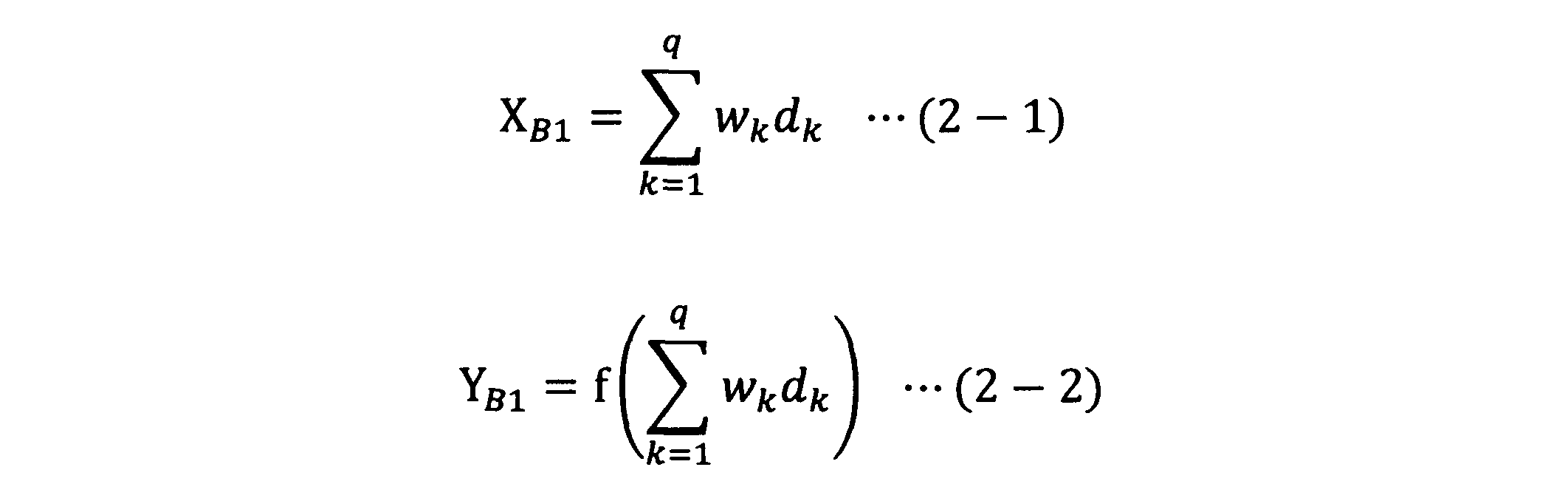
関数fは、活性化関数を表している。Σは、重み係数w1~wqと、入力データd1~dqとの積和演算(重み付け合計)を表している。ここでは中間ノードB1の演算例を示したが、中間ノードB2~Bjでも同様の演算が行われる。中間ノードB1~Bjの出力値は、出力ノードC1~Cmに入力されるデータとなる。
活性化関数は、例えば、ReLU関数又はステップ関数など、任意の非線形関数が用いられる。但し、線形関数を用いることも排除されない。
ReLU関数は、入力変数が0以下であれば0を出力し、0を超えていれば入力変数の値をそのまま出力する関数である。ReLU関数をReLu(x)、入力変数をxとすると、ReLu(x)は、以下のように定義される。

ステップ関数は、入力変数が0以下であれば0を出力し、0を超えていれば1を出力する関数である。ステップ関数をStep(x)、入力変数をxとすると、Step(x)は、以下のように定義される。

中間層における各中間ノードの活性化関数は同じであるとするが、中間ノードによって活性化関数が異なっていてもよい。
各出力ノードの演算は、中間ノードの演算と同様である。より詳細には、各出力ノードは、中間ノードB1~Bjから入力されたデータに、中間ノードB1~Bjに対する重み係数を乗算し、乗算結果を総和する。すなわち、入力されたデータと重み係数との積和演算(重み付け合計)を行う。積和演算の結果を活性化関数の入力変数とし、活性化関数を計算する。各出力ノードにおける活性化関数の出力値が、各出力ノードの出力となる。
出力層の各出力ノードの活性化関数は同じであるとするが、出力ノードによって活性化関数が異なってもよい。また出力層の活性化関数は、中間層の活性化関数と異なっていても、同じであってもよい。
演算処理部19は、各出力ノードの出力値に基づき、判定処理を行い、判定処理の結果を、画像認識の結果として出力する。
一例として、各出力ノードにクラスが割り当てられており、最も大きい出力値を出力した出力ノードのクラスを識別結果とする。例えば2つの出力ノードが存在し、一方の出力ノード(第1出力ノード)に割り当てられた第1クラスが画像に人の顔が写っていることを表すクラスであるとする。そして、他方の出力ノード(第2出力ノード)に割り当てられた第2クラスが画像に人の顔が写っていないことを表すクラスであるとする。この場合、第1出力ノードの出力値が第2出力ノードの出力値より大きければ、第1クラスを示す信号を出力する。すなわち、ニューラルネットワークに入力として与えられた画像データに人の顔が写っていると判定する。第2出力ノードの出力値が第1出力ノードの出力値より大きければ、第2クラスを示す信号を出力する。すなわち、ニューラルネットワークに入力として与えられた画像データに人の顔は写っていないと判定する。
上述の各出力ノードの出力値に基づく判定処理は一例であり、他の判定処理も可能である。例えば各出力ノードの出力値を閾値と比較し、閾値以上の出力値が得られた出力ノードの個数の割合が一定値以上の場合は、第1の識別結果を決定する(例えば画像に人の顔が写っていると判定)。当該割合が一定値未満の場合は、第2の識別結果を決定する(例えば画像に人の顔が写っていないと判定)。あるいは、出力ノードの出力値のうち最も大きな出力値を特定し、特定した出力値が一定値以上の場合、第1の識別結果を決定し、一定値未満の場合は、第2の識別結果を決定してもよい。閾値は予めデータ記憶部18又は演算処理部19の内部バッファに格納しておく。各出力ノードの出力値に基づく判定方法は、ニューラルネットワークの構成や学習方法等に応じて任意に定義することができる。
中間層が複数存在する場合は、初段の中間層の各中間ノードが、入力ノードA1~Aqの全てとリンクで結合され、各リンクには重み係数が設定される。また、隣接する中間層同士間で、後段の中間層の各中間ノードが、前段の中間層の全ての中間ノードとリンクで結合され、各リンクには重み係数が設定される。出力層43の各出力ノードが、最終段の中間層の全ての中間ノードとリンクで結合され、各リンクには重み係数が設定される。2段目以降の中間層の各中間ノードでは、前段の中間層の全ての中間ノードの出力値が、入力されるデータとなる。2段目以降の中間層の各中間ノードの演算は、前述した中間層42と同様である。
このようなニューラルネットワークの学習は、予め識別結果(正解)が分かっている複数の画像データを学習データとして用意し、画像データを入力層に入力したら、当該識別結果(正しい識別結果)が得られるよう、ノード間の重み係数を調整することで行う。予め分かっている識別結果は教師信号と呼ばれる。このような重み係数の調整は、バックプロパゲーション法(誤差逆伝播法:Back Propagation Method)などの方法を用いて行えばよい。バックプロパゲーション法は、ニューラルネットワークの出力と教師信号のずれが小さくなるよう、出力層側から順番に、重み係数を調整する方法である。
以上は、一般的なニューラルネットワークの説明であるが、以下、図4~図6を用いて、本実施形態に係るニューラルネットワークについて説明する。図4は一般的なニューラルネットワークの説明で用いたものであるが、ニューラルネットワークの構造を普遍的に示したもので、本実施形態に係るニューラルネットワークの説明も図4をベースに行う。本実施形態に係るニューラルネットワークは、一例として第1ニューラルネットワークに対応し、第1ニューラルネットワークにおける各ノードは一例として第1ノードに対応する。
本実施形態ではニューラルネットワークの各入力ノードに与えるデータとして、演算処理部19が、画素データをデータ変換し、これを入力データ(第1入力データ)として用いる。より詳細には、各画素21の画素データが示す値(電圧値)に対して、上述の式(1)の関係にある電流値iを底2の対数に変換したデータ(log2i)を用いる。変換したデータを、対数画素データと呼ぶ。上述の式(1)を、底の変換公式を用いて、式(5-1)のように変換し、さらに式(5-2)のように変換することで、対数画素データ(log2i)を導出できる。

A及びlog2eのいずれも固定値であるから、A’も固定値である。よって、画素データの値(v)にA’を乗じることで、log2iを算出できる。A’は固定値であるから、この演算は簡単であり、小規模の演算量又は小規模の回路で実現できる。すなわち、画素データを底が2の対数に変換(log2変換)するための回路(log2変換回路)は不要である。log2eは、所定値(ここではネイピア数)を真数に含む対数の一例である。
また、本実施形態に係るニューラルネットワークの演算処理では、各ノード間の重み係数として、学習された重み係数を底2の対数に変換した対数重み係数を用いる。各ノード間とは、入力ノード及び中間ノード間、並びに、中間ノード及び出力ノード間のことである。中間層が複数存在する場合は、異なる中間層間での中間ノード間も含む。このように、本実施形態に係るニューラルネットワークの演算処理は、各入力ノードに与えられる対数画素データと、各ノード間に設定される対数重み係数とに基づき行われる。
以下、中間ノードの演算処理の内容を説明する。まず、中間ノードに接続されている各入力ノードから入力される対数画素データと、各入力ノードに対する対数重み係数とをそれぞれ加算する。加算の対象がいずれも対数であるから、加算結果も対数である。log2i+log2w=log2(i*w)が成立するから、対数画素データ(log2i)と対数重み係数(log2w)を加算した値は、電流データiと重み係数wとの乗算値(i*w)を、底2の対数に変換した値に等しい。i*wを直接計算することなく、入力された対数同士を加算するのみでlog2(i*w)を算出できる。よって、一般的なニューラルネットワークの演算処理における乗算演算を、加算演算に置き換えることができる。
次に、各入力ノードに対する加算結果(対数値)の真数の総和値のlog2を算出する。複数の対数値の真数を総和した値のlog2を算出することを、“log2加算”と呼ぶ。また、log2加算により算出された値をlog2加算値と呼ぶ。
例えば、各入力ノードに対する加算結果をlog2(i1*w1),・・・,log2(iq-1*wq-1),log2(iq*wq)とすると、これらのlog2加算値は、log2(i1*w1+,・・・,+iq-1*wq-1+iq*wq)である。log2加算は、小規模の演算量又は小規模の回路で実現できる。
算出したlog2加算値を活性化関数の入力変数として、活性化関数の出力値を計算する。以下、図4の中間ノードB1を例に、具体例を説明する。
図5は、中間ノードB1の演算処理の例を説明するための図である。中間ノードB1と、入力ノードA1~Aqとの間に設定された対数重み係数をlog2w1~log2wqとする。入力ノードA1~Aqから中間ノードB1に入力されるデータをlog2i1~log2iqとする。このとき、中間ノードB1における演算値(X’B1)、活性化関数の出力値(Y’B1)は、以下の式で表される。図5の例では活性化関数としてReLU関数を用いている。
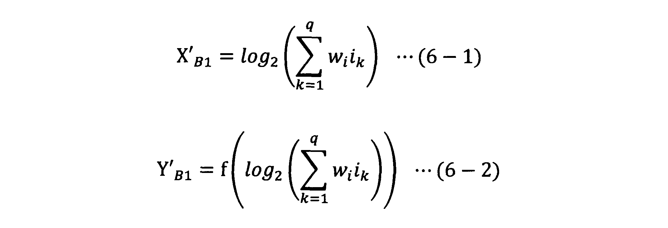
中間ノードB2~Bjでも、中間ノードB1と同様の演算が行われる。
式(6-1)と式(2-1)とを比較して理解できるように、本実施形態に係るニューラルネットワークにおけるノードの演算値(log2加算値)は、一般的なニューラルネットワークにおけるノードの演算値(積和演算値)をlog2に変換した値に相当する。
出力ノードC1~Cnの演算処理も、前段の層から入力されるデータが、各中間ノードの出力値である以外は、中間ノードと同様である。中間ノードの出力値は底2の対数であるから、出力ノードでも、中間ノードと同様にlog2加算の演算を行うことができる。
例えば、中間ノードにおける活性化関数がReLUの場合、演算値が0より大きい場合は、当該値がそのまま出力されるため、ReLUの出力値は底2の対数である。演算値が0以下の場合、0が出力されるが、0=log21であるから、この場合も出力値は底2の対数で表される。よって、出力ノードでも、中間ノードと同様の演算を行うことができる。
演算処理部19は、出力ノードC1~Cnの出力値(底が2の対数)に基づき判定処理を行い、判定処理の結果を、画像認識の結果として出力する。判定処理の詳細は、前述した一般的なニューラルネットワークの判定処理と同様である。例えば、各出力ノードにクラスが割り当てられており、最も大きい出力値を出力した出力ノードのクラスを画像認識の結果とする。その他、前述した各出力ノードの出力値を閾値と比較する方法も可能である。閾値と比較する場合、閾値を底2の対数に変換した値(対数閾値)を用いればよい。これにより、対数同士で比較が可能となる。対数閾値は予めデータ記憶部18又は演算処理部19の内部バッファに格納しておく。
このように本実施形態に係るニューラルネットワークでは、中間ノード及び出力ノードで乗算演算は不要であるため、乗算回路が不要となり、回路規模も低減される。また、演算量が低減されるため、消費電力も低減される。
ここでlog2加算の演算を効率的に行うための回路(log2加算回路)の構成例について説明する。ここで、log2(i1*w1)とlog2(i2*w2)とのlog2加算は、以下の式で近似できる(非特許文献1参照)。

式(7)の最初の項は、log2(i1*w1)とlog2(i2*w2)のうちの最大値を意味する。2番目の項は、log2(i1*w1)とlog2(i2*w2)の差分の絶対値のマイナスだけ2を累乗している。2番目の項は1を、当該差分の絶対値だけ右側(桁の小さい方向)にビットシフトすることに等しい。つまり、10進数の1をビットで表記したビット列を、|log2(i1*w2)-log2(i1*w1)|だけ右側にビットシフトする。ビットシフトを右側に行うのは、2のべき乗の指数が負の値であるためである。例えば、1が00001000と表される場合に、上述の差分の絶対値が3であれば、3ビットシフトを行うことにより、00000001となる。なおビット表記の規則は任意に定めればよく、本例は一例に過ぎない。
このように、最大値の選択と、差分の絶対値の計算と、ビットシフトによりlog2加算ができるため、演算が簡単である。なお、|log2(i1*w2)-log2(i1*w1)|の値が整数にならない場合は、丸め処理(切り上げ又は切り捨て)、天井関数又は床関数などにより整数に近似すればよい。あるいは、log2(i1*w2)及びlog2(i1*w1)をそれぞれ整数に近似してから、|log2(i1*w2)-log2(i1*w1)|を計算してもよい。
図6は、log2加算回路の一例のブロック図である。log2加算回路は演算処理部19に含まれている。ここでは複数の入力ノードA1~Aqに対してそれぞれ対数画素データと対数重みとの加算により計算されたlog2(in*wn)(nは1~qの整数)を、累積加算する場合の回路構成の例を示している。図6の回路は、セレクタ51と、加算器52と、減算器53と、絶対値演算器54と、べき乗演算器55と、フリップフロップ回路56とを備えている。
セレクタ51は第1入力端子と第2入力端子とを有する。第1入力端子には新たに演算対象となるlog2(in*wn)が入力され、これをデータPnと表す。第2入力端子には前回まで累積加算された値log2(i1*w1+・・・+in-1*wn-1)が入力され、これをデータSn-1と表す。初回は、第1入力端子にlog2(i2*w2)(=P2)が入力され、第2入力端子にlog2(i1*w1)(=S1)が入力される。
データPnとデータSn-1は減算器53にも入力される。減算器53は、PnからSn-1を減算する。減算器53の出力は、セレクタ51の制御端子に接続されている。減算器53は、減算結果の符号を示す信号をセレクタ51の制御端子に出力し、減算結果を表す信号を絶対値演算器54に出力する。セレクタ51は、減算結果が正を示す場合はデータPnを出力し、負を示す場合は、データSn-1を出力する。すなわち、データPnとSn-1のうち大きい方を出力する。減算器53は、Sn-1からPnを減算する構成でもよく、この場合、セレクタ51は、減算結果が正を示す場合はデータSn-1を出力し、負を示す場合は、データPnを出力すればよい。
絶対値演算器54は、減算器53の出力に接続されており、減算器53の減算結果の絶対値|Pn-Sn-1|を計算する。
べき乗演算器55は、絶対値演算器54の出力に接続されており、2の-|Pn-Sn-1|乗を計算する。この計算は上述したように、1を|Pn-Sn-1|だけ、右側にビットシフトすることにより実現できる。
加算器52は、セレクタ51の出力とべき乗演算器55の出力に接続されており、セレクタ51で選択された値と、べき乗演算器55でビットシフトされた後の値とを加算する。
フリップフロップ回路56は、加算器52の出力に接続されており、加算器52の加算結果(log2(i1*w1+i2*w2)の近似値)を内部に記憶する。フリップフロップ回路56は、セレクタ51の第2入力端子に接続されており、この値をデータS2として第2入力端子及び減算器53にフィードバックする。セレクタ51の第1入力端子には次に演算対象となるlog2(i3*w3)がデータP3として入力される。以降、同様にして処理を繰り返すことで、log2(in*wn)が累積的にlog2加算され、最終的に、log2(i1*w1+・・・+iq*wq)の近似値が、クロックCLKで動作するフリップフロップ回路56から出力される。フリップフロップ回路56の出力値は、活性化関数の入力変数となる。
図7は、本実施形態に係る固体撮像装置の動作の一例のフローチャートである。本装置を搭載したデバイスで予め定めたイベントが成立したことにより、本処理の実行のトリガーが発生する。予め定めたイベントは、本装置を搭載したデバイスで発生又は検知するイベントであれば何でもよい。例えば、本装置を搭載したデバイスを操作するユーザが所定の操作を行ったこと、所定の時刻になったこと、一定値以上の振動を検知したことなどがあるが、これらに限定されない。このトリガーにより、制御部15の制御の元、画素アレイ部11で1フレームの撮像が行われる。すなわち、各画素21で光電変換により、入射光の光量に対して対数的に変化する画素信号(電圧信号)が生成され、生成された画素信号を読み出して信号処理部16に送る(S101)。これらの画素信号をカラム処理部13でAD変換し(S102)、AD変換により得られた各画素の画素データの集合を、画像データとしてデータ記憶部18に格納する(S103)。
演算処理部19は、データ記憶部18から画像データを読み出し、画像データに含まれる各画素データに対してデータ変換を行う(S104)。データ変換操作は、一例としてlog2e/Aを乗じることである(式(5-1)と式(5-2)参照)。すなわちネイピア数(所定値)を真数に含む対数を、画素データの値に乗じる。これにより、画素データの値を底2の対数に変換したデータ(log2i)を、対数画素データとして算出する(同S104)。
演算処理部19は、データ記憶部18から、ニューラルネットワークにおける各ノード間に設定された重み係数の対数である対数重み係数(log2重み係数)を読み出す(S105)。各ノード間とは、入力ノード及び中間ノード間、並びに、中間ノード及び出力ノード間のことである。中間層が複数存在する場合は、異なる中間層間での中間ノード間も含む。対数重み係数は、データ記憶部18でなく、演算処理部19の内部バッファに予め記憶させておいてもよい。以下の説明では、中間層が1つのニューラルネットワーク(図4参照)を想定するが、複数の場合も可能である。この場合、2段目以降の中間層では、入力されるデータが入力ノードからではなく、前段の中間層の中間ノードからに変更されるのみで、処理の内容は初段の中間層と同様である。
演算処理部19は、各画素21の対数画素データを入力データとしてニューラルネットワークの各入力ノードに割り当てる(S106)。どの入力ノードにどの画素21が対応付けられるかは学習時に予め定めておく。画素21と入力ノードとを1対1で対応づけることは一例に過ぎず、他の手法で、各入力ノードに割り当てる入力データを生成してもよい。
例えば、所定個数の画素21により画素グループを構成し、各画素グループを各入力ノードに対応づける。画素グループで対数画素データの代表値を決定し、代表値を入力データとして入力ノードに割り当てる。代表値は、平均値、最大値又は最小値など任意の統計値でよい。また、今回読み出した対数画素データと、前回読み出した対数画素データとの差分の画素データを入力データとして入力ノードに割り当てることも可能である。
演算処理部19は、各入力ノードに割り当てた入力データと、各中間ノード及び各入力ノード間に設定された対数重み係数とに基づき、各中間ノードの演算を行う(S107)。すなわち、各入力ノードに対して対数重み係数と入力データとを加算し、加算結果を全てlog2加算する。演算処理部19は、log2加算値を入力変数として、活性化関数を計算する(同S107)。活性化関数の出力値を、各中間ノードの出力値とする。各中間ノードの出力値は、次段の出力層に入力されるデータとなる。
次に、各中間ノードの出力値と、各中間ノード及び各出力ノード間に設定された対数重み係数とに基づき、各出力ノードの演算を行う(S108)。すなわち、各中間ノードに対して、対数重み係数と入力されるデータとを加算し、加算結果を全てlog2加算する。演算処理部19は、log2加算値を入力変数として、活性化関数を計算する(同S108)。活性化関数の出力値が、出力ノードの出力値となる。
演算処理部19は、各出力ノードの出力値に基づき、判定処理を行う(S109)。一例として、最も大きい出力値を算出した出力ノードを特定し、特定した出力ノードに割り当てられているクラスを画像認識の結果として取得する。判定認識は、前述したように、閾値を用いた処理など、その他にも様々なアルゴリズムが可能である。どのようなアルゴリズムを用いてもかまわない。演算処理部19は、画像認識の結果を示すデータをデータ記憶部18に格納する。
CPU17は、画像認識の結果を示すデータをデータ記憶部18から読み出して、外部に出力する(S110)。例えば、本装置が搭載されたデバイスで実行されているアプリケーションプログラムに出力する。この場合、アプリケーションプログラムは、当該データが示す結果に応じた処理を行う。また、画像認識の結果を示すデータを、本装置が搭載されたデバイスが備える表示装置の画面に表示してもよい。
上述のステップの順序は一例であり、一部のステップの順序が入れ替わってもよい。例えばステップS104とステップS105の順序が逆でもよい。
以上、本実施形態によれば、対数画素から読み出した画素信号(電圧信号)のデータをデータ変換することにより、底2の対数の入力データを生成する。よって、底2の対数への変換を行う回路(log2変換回路)は必要がないため、回路規模を低減できるとともに、消費電力を低減できる。
本実施形態では対数画素から読み出した画素信号のデータを用いるため、対数画素がもつ高ダイナミックレンジの特性を生かした画像認識が可能となる。関連技術では線形画素から読み出した画素信号のデータをlog2変換回路で底2の対数に変換するが、この場合、変換後のデータのダイナミックレンジは線形画素のダイナミックレンジに律速される。このため、高ダイナミックレンジの効果は得られない。これに対して、本実施形態では対数画素からの読み出しを行うため、高ダイナミックレンジの効果を得ることができる。
また本実施形態によれば、画素データを変換した対数画素データ(底2の対数)と、対数重み係数(底2の対数)とを用いるため、各ノードでの演算を加算で行うことができる。よって、各ノードでの乗算(重み係数と入力データとの乗算)が不要となる。よって、演算量が低減し、消費電力を低減できる。また、乗算回路が不要となるため、回路規模を低減できる。
(変形例1)
第1の実施形態では、底2の対数を用いたが、対数の底は必ずしも2である必要はない。底が2でない場合も、各ノードで対数領域での加算演算を行うことで、演算量を低減することが期待できる。
第1の実施形態では、底2の対数を用いたが、対数の底は必ずしも2である必要はない。底が2でない場合も、各ノードで対数領域での加算演算を行うことで、演算量を低減することが期待できる。
(変形例2)
第1の実施形態で示した対数画素の構成(図3)は一例であり、様々な変形が可能である。図8を用いて、対数画素の変形例を説明する。
第1の実施形態で示した対数画素の構成(図3)は一例であり、様々な変形が可能である。図8を用いて、対数画素の変形例を説明する。
図8は、対数画素の変形例を示す回路図である。図3の対数画素に画素トランジスタとして、リセットトランジスタ37、バッファトランジスタ38及びバイアストランジスタ39が追加されている。バッファトランジスタ38及びバイアストランジスタ39はバッファ回路40を構成する。リセットトランジスタ37は、一例としてN型トランジスタにより構成される。バッファトランジスタ38及びバイアストランジスタ39は、一例としてP型トランジスタにより構成される。
接続ノードN2は、出力トランジスタ32のゲート端子と、バッファトランジスタ38のゲート端子とに接続されている。接続ノードN2に生成される電圧信号は、バッファ回路40を介して増幅トランジスタ35に与えられる。この電圧信号が増幅トランジスタ35により増幅される。
電源電圧と基準電圧との間に、バイアストランジスタ39とバッファトランジスタ38が直列に接続されている。バイアストランジスタ39のゲート端子にはバイアス電圧Vbias2が印加されている。バイアストランジスタ39とバッファトランジスタ38の接続ノード、すなわちバッファ回路40の出力端子は、リセットトランジスタ37のソース端子と、増幅トランジスタ35のゲート端子とに接続されている。リセットトランジスタ37のドレイン端子は電源電圧に接続されている。リセットトランジスタ37のゲート端子は画素駆動線22に接続されている。
リセットトランジスタ37は、垂直駆動部12が供給するリセット信号RSTにより制御される。リセットトランジスタ37をオン状態にして、画素信号を含まない信号を検出し、検出した信号を画素信号から除去(減算)するCDS(Correlated Double Sampling)処理を、信号処理部16又はカラム処理部13で行う。これにより、画素トランジスタ等のばらつきにより生じる固定パターンノイズを除去する。なお画素信号の読み出しは、画素信号を含まない信号を読み出す前又は後に行えばよい。CDS処理により得られた信号を、対数画素から読み出した画素信号として用いることができる。なお、バッファ回路40は、リセット時に対数画素の電位(ノードN2の電位)が影響を受けることを低減するよう機能する。これにより対数画素の電位を、常時光量に依存した出力にすることができる。なお、図8の回路構成を用いつつも、CDS処理を行わないことも可能である。
本変形例によれば、CDS処理を行うことにより、画素信号に含まれる固定パターンノイズを除去することができる。
(変形例3)
図9は、対数画素の他の変形例を示す回路図である。図8の回路構成に対してイベント検出部80が追加されている。イベント検出部80が追加された画素回路をDVS(Dynamic Vision Sensor)回路と呼ぶ場合もある。なおバッファ回路40の構成を、ここでは記号により模式的に示している。イベント検出部80は、フォトダイオード31からの光電流の変化量が所定の閾値を超えたか否かにより、イベントの有無を検出する。イベントの例として、変化量が上限の閾値を超えたオンイベント、変化量が下限の閾値を下回るイベント、又はこれらの両方がある。オンイベント又はオフイベントの検出は、一例として、コントラストの変化を検出(例えば物体を検出)することに相当する。イベント検出部80は、イベントの検出有無に応じて検出信号又は非検出信号を制御部15に出力する。
図9は、対数画素の他の変形例を示す回路図である。図8の回路構成に対してイベント検出部80が追加されている。イベント検出部80が追加された画素回路をDVS(Dynamic Vision Sensor)回路と呼ぶ場合もある。なおバッファ回路40の構成を、ここでは記号により模式的に示している。イベント検出部80は、フォトダイオード31からの光電流の変化量が所定の閾値を超えたか否かにより、イベントの有無を検出する。イベントの例として、変化量が上限の閾値を超えたオンイベント、変化量が下限の閾値を下回るイベント、又はこれらの両方がある。オンイベント又はオフイベントの検出は、一例として、コントラストの変化を検出(例えば物体を検出)することに相当する。イベント検出部80は、イベントの検出有無に応じて検出信号又は非検出信号を制御部15に出力する。
イベント検出部80は、減算器81と量子化器82とを含む。バッファ回路40の出力端子に減算器81が接続されている。減算器81の出力端子に量子化器82が接続されている。なお、イベント検出部80を図3の回路構成に追加することも可能である。
減算器81は、垂直駆動部12からの駆動信号に従ってバッファ回路40からの電圧信号のレベルを低下させる。この減算器81は、低下後の電圧信号を量子化器82に供給する。
量子化器82は、減算器81からの電圧信号をデジタル信号に量子化する。量子化器82は、量子化後の信号を閾値電圧Vthと比較し、比較結果を示す信号(検出信号又は非検出信号)を生成する。一例として、閾値電圧Vthが上限の閾値であれば、量子化後の信号が上限の閾値より大きい場合は、検出信号を生成する。量子化後の信号が上限の閾値以下であれば、非検出信号を生成する。量子化器82は、生成した検出信号又は非検出信号を、制御部15に出力する。閾値電圧Vthが下限の閾値の場合も同様にして、検出信号又は非検出信号を生成することができる。
制御部15は、検出信号が入力された場合は、対数画素21からの画素信号の読み出しを行うことを決定し、対数画素21から画素信号の読み出しを行うよう垂直駆動部12を制御する。一方、制御部15は、非検出信号が入力された場合は、対数画素21からの画素信号の読み出しを行わないことを決定する。なお、量子化器82はイベントが検出されなかった場合に、制御部15への非検出信号の出力を省略する構成も可能である。
図10は、減算器81および量子化器82の一構成例を示す回路図である。減算器81は、コンデンサ83と、コンデンサ84と、インバータ85と、スイッチ86とを備える。量子化器82は、コンパレータ87を備える。
コンデンサ83の一端は、バッファ回路40の出力端子に接続され、他端は、インバータ85の入力端子に接続される。コンデンサ84は、インバータ85に並列に接続される。スイッチ86は、コンデンサ84の両端を接続する。スイッチ86は、垂直駆動部12からの駆動信号に従って開閉する。
インバータ85は、コンデンサ83を介して入力された電圧信号を反転する。インバータ85は、反転した信号をコンパレータ87の非反転入力端子(+)に出力する。
スイッチ86がオンされると、コンデンサ83のバッファ回路40側に電圧信号Vinitが入力され、その逆側は仮想接地端子となる。この仮想接地端子の電位を便宜上、ゼロとする。このとき、コンデンサ83の容量をC1とすると、コンデンサ83に蓄積されている電荷Qinitは、次の式により表される。一方、コンデンサ84の両端は、短絡されているため、その蓄積電荷はゼロとなる。
Qinit=C1×Vinit ・・・(8-1)
Qinit=C1×Vinit ・・・(8-1)
次に、スイッチ86がオフされて、コンデンサ83のバッファ回路40側の電圧が変化してVafterになる。このときコンデンサ83に蓄積される電荷Qafterは、次の式により表される。
Qafter=C1×Vafter ・・・(8-2)
Qafter=C1×Vafter ・・・(8-2)
一方、コンデンサ84に蓄積される電荷Q2は、出力電圧をVoutとすると、次の式により表される。
Q2=-C2×Vout ・・・(8-3)
Q2=-C2×Vout ・・・(8-3)
コンデンサ83およびコンデンサ84の総電荷量は変化しないため、次の式が成立する。
Qinit=Qafter+Q2 ・・・(8-4)
Qinit=Qafter+Q2 ・・・(8-4)
式(8-4)に、式(8-1)~式(8-3)を代入して変形すると、次の式が得られる。
Vout=-(C1/C2)×(Vafter-Vinit) ・・・(8-5)
Vout=-(C1/C2)×(Vafter-Vinit) ・・・(8-5)
式(8-5)は、電圧信号の減算動作を表し、減算結果の利得はC1/C2となる。通常、利得を最大化することが望まれるため、C1を大きく、C2を小さく設計することが好ましい。一方、C2が小さすぎると、kTCノイズが増大し、ノイズ特性が悪化するおそれがあるため、C2の容量削減は、ノイズを許容することができる範囲に制限される。
コンパレータ87は、減算器81からの電圧信号と、反転入力端子(-)に印加された閾値電圧Vthとを比較する。コンパレータ87は、比較結果に応じて検出信号又は非検出信号を出力する。
本変形例によれば、イベント検出部80によりイベントを検出したときに画素信号の読み出しを行うため、高速な画素データの生成が可能となる。
(第2の実施形態)
本実施形態では、画素アレイ部11に配置する画素として、対数画素と線形画素との2種類を用いる。そして、外部から与えられる指示データに従って、画素信号を読み出す画素を、対数画素及び線形画素間で選択する。対数画素から画素信号を読み出す場合は、その後の処理は第1の実施形態と同様である。線形画素から画素信号を読み出す場合は、その後の処理は、一般的なニューラルネットワークの演算処理と同様である。すなわち、各ノード(中間ノード及び出力ノード)で、各画素の画素データと、重み係数とに基づき積和演算を行い、積和演算の結果を入力変数として活性化関数を計算する。以下、本実施形態について詳細に説明する。
本実施形態では、画素アレイ部11に配置する画素として、対数画素と線形画素との2種類を用いる。そして、外部から与えられる指示データに従って、画素信号を読み出す画素を、対数画素及び線形画素間で選択する。対数画素から画素信号を読み出す場合は、その後の処理は第1の実施形態と同様である。線形画素から画素信号を読み出す場合は、その後の処理は、一般的なニューラルネットワークの演算処理と同様である。すなわち、各ノード(中間ノード及び出力ノード)で、各画素の画素データと、重み係数とに基づき積和演算を行い、積和演算の結果を入力変数として活性化関数を計算する。以下、本実施形態について詳細に説明する。
図11は、本開示の第2の実施形態に係る固体撮像装置の構成例を示すブロック図である。図1の固体撮像装置に対して、入出力端子24とモード指示部25が追加されている。図1と同一名称の要素には同一の符号を付して、拡張又は変更された処理を除き、詳細な説明は適宜省略する。
画素アレイ部11は、対数画素21Aと線形画素21Bとの2種類の画素を含む。線形画素21Bは、対数画素21Aと異なる種類の画素である第2画素の一例に対応する。また、線形画素21Bから読み出される画素信号は、第2画素から読み出される第2画素信号に対応する。
対数画素21Aと線形画素21Bは、横及び縦のそれぞれの方向に交互に配置(千鳥格子状に配置)されている。但し、配置の方法はこれに限定されず、どのような方法でもよい。例えば、縦2つ及び横2つの画素からなる正方形状の画素ブロックごとに、画素ブロック内の3つの画素が対数画素であり、残りの1つが線形画素であってもよい。また列ごとに画素の種類を同じとして、行方向(横方向)に交互に異なる種類の画素列が配置されてもよい。
第1の実施形態の説明で記載したように、線形画素は、入射光に対して線形に変化する電気信号を画素信号として生成する。すなわち、線形画素は、光量に対して線形に増大する出力信号を生成する。線形画素は、対数画素に比べて、ダイナミックレンジが狭いものの、低ノイズ特性を有している。
図12に、線形画素への入射光の光量と、出力電圧との関係を模式的に表したグラフを示す。入射光の光量が増大するに応じて、出力電圧が、線形に増加(例えば比例)している。
図13は、線形画素21Bの回路構成の一例を示す。ここでは例示として、1つの線形画素21Bの構成を示すが、他の線形画素21Bも同様の構成を有する。
線形画素21Bは、光電変換部に対応するフォトダイオード61と、複数の画素トランジスタとを含む。複数の画素トランジスタは、転送トランジスタ62、増幅トランジスタ63、選択トランジスタ64、及びリセットトランジスタ65である。これらの画素トランジスタは、MOS(Metal Oxide Semiconductor)トランジスタであり、一例としてN型トランジスタで構成されている。但し、これらのトランジスタがP型トランジスタで構成されてもよい。この場合、これらの画素トランジスタの制御信号の論理及び電源線の電圧を変更する必要がある。
フォトダイオード61は、入射光を光電変換によりその光量に比例した電気信号(信号電荷)に変換して蓄積する素子である。フォトダイオード61のアノード端子が基準電圧に接続されており、カソード端子が転送トランジスタ62のソース端子に接続されている。
転送トランジスタ62は、フォトダイオード61のカソード端子とFDノード66との間に接続されている。転送トランジスタ62のゲート端子は、垂直駆動部12に接続されている。転送トランジスタ62は、垂直駆動部12からの転送信号TRGによって制御される。転送トランジスタ62がオン状態になると、フォトダイオード61に蓄積されている信号電荷がFDノード66に転送される。
FDノード66は、転送トランジスタ62のドレイン端子と増幅トランジスタ63のゲート端子との間に接続された浮遊拡散領域である。これにより、FDノード66は、フォトダイオード61から転送される信号電荷を蓄積することがきる。また、FDノード66は、リセットトランジスタ65のソース端子にも接続されている。
増幅トランジスタ63は、電源電圧と選択トランジスタ64との間に接続されている。増幅トランジスタ63のゲート端子は、FDノード66に接続されている。増幅トランジスタ63は、FDノード66に蓄積された信号電荷に応じた導通状態となる。
選択トランジスタ64は、増幅トランジスタ63と垂直信号線23との間に接続されている。選択トランジスタ64のゲート端子は、垂直駆動部12に接続されている。選択トランジスタ64は、垂直駆動部12からの選択信号SELによって制御される。選択トランジスタ64は、線形画素21Bを垂直信号線23に接続しあるいは切断する。選択トランジスタ64がオン状態になると、増幅トランジスタ63に電流を流すことが可能となり、増幅トランジスタ63の導通状態に応じた電流が、電源電圧から流れる。垂直信号線23は、増幅トランジスタ63のゲート電圧の信号レベルに応じた電圧にされる。
リセットトランジスタ65は、電源電圧とFDノード66との間に接続されている。リセットトランジスタ65のゲート端子は、垂直駆動部12に接続されている。リセットトランジスタ65は、垂直駆動部12からのリセット信号RSTによって制御される。リセットトランジスタ65がオン状態になると、FDノード66に蓄積されていた信号電荷は電源電圧に排出される。これにより、線形画素21BのFDノード66がリセット状態となる。
このように線形画素では、入射光の光量に比例する電圧信号が、画素信号として出力される。図13に示した線形画素の構成は一例であり、線形画素の構成は図13の構成に限定されない。光量(電荷)に比例する電圧信号を検出可能である限り、どのような構成でもかまわない。
入出力端子24は、外部の装置との信号の送受信を行うための端子である。入出力端子24は、例えばシリアル通信などの任意の通信方式により、外部の装置と信号を送受信する。外部の装置は、一例として、固体撮像装置を搭載したデバイスの内部設定をデバイスの外部から行う装置でもよいし、ユーザが各種設定を行うための操作手段(例えばボタンなど)でもよい。
モード指示部25は、入出力端子24を介して、画素の読み出し処理のモードを指示したモードデータを受信する。画素読み出しモードには、対数読出モードと、線形読出モードがある。対数読出モードは、対数画素からの読み出しを行う第1読出処理を行う。線形読出モードは、線形画素からの読み出しを行う第2読出処理を行う。モードデータはこれらのいずれかのモードを指示している。モード指示部25は、一例としてレジスタなどの記憶素子により構成される。モード指示部25へのモードデータの提供をCPU17が行う構成も可能である。
制御部15は、モード指示部25からモードデータを読み出し、モードデータが対数読出モードを示す場合は、画素アレイ部11における各対数画素21Aから画素信号の読み出しを行うよう各部を制御する。制御部15は、モードデータが線形読出モードを示す場合は、画素アレイ部11における各線形画素21Bから画素信号の読み出しを行うよう各部を制御する。すなわち、制御部15は、各対数画素21Aから画素信号を読み出す処理と、各線形画素21Bから画素信号を読み出す処理とを選択的に実行する。
カラム処理部13は、第1の実施形態と同様、1行分の画素21から出力される信号の信号処理を、画素列ごとに行う。信号処理の例は、AD変換を含み、さらにAD変換前の信号のノイズ除去及び信号増幅の少なくとも一方を含んでもよい。
データ記憶部18は、演算処理部19がニューラルネットワークの演算処理で用いるニューラルネットワークのパラメータを、対数読出モード及び線形読出モードのそれぞれ用に記憶している。対数読出モード及び線形読出モードのニューラルネットワークはそれぞれ異なり、学習もそれぞれ別に行われる。
データ記憶部18は、対数読出モード用のニューラルネットワークのパラメータとして、第1の実施形態と同様に、各ノード間の結合の強さを表す重み係数を、底を2とする対数に変換した値(対数重み係数)を記憶している。対数重み係数をデータ記憶部18ではなく、演算処理部19の内部バッファに記憶してもよい。対数読出モード用のニューラルネットワークは、一例として第1ニューラルネットワークに対応し、第1ニューラルネットワークにおける各ノードは一例として第1ノードに対応する。
データ記憶部18は、線形読出モード用のニューラルネットワークのパラメータとして、各ノード間の結合の強さを表す重み係数を記憶している。重み係数をデータ記憶部18ではなく、演算処理部19の内部バッファに記憶してもよい。線形読出モード用のニューラルネットワークは、一例として第2ニューラルネットワークに対応し、第2ニューラルネットワークにおける各ノードは一例として第1ノードに対応する。
CPU17は、モード指示部25からモードデータを読み出し、モードデータが対数読出モードを示す場合は、第1の実施形態と同様に、演算処理部19の制御を行う。すなわち、演算処理部19は、各画素の画素データを対数画素データに変換し(式(5-2)参照)、対数画素データと、各ノード間の対数重み係数とを用いて、ニューラルネットワークの演算処理を行う。各中間ノード及び各出力ノードでは、第1の実施形態の説明で記載したように、前段の層から入力されるデータと対数重み係数とを加算し、これらの加算結果をlog2加算する(式(6-1)参照)。log2加算の結果を活性化関数の入力変数として、活性化関数の出力値を計算する(式(6-2)参照)。
CPU17は、モードデータが線形読出モードを示す場合は、第1の実施形態の説明で記載した一般的なニューラルネットワークと同様の演算を行うように、演算処理部19を制御する。すなわち、演算処理部19は、各画素の画素データをニューラルネットワークの入力データ(第2入力データ)とし、当該入力データと、各ノード間の重み係数とを用いて、ニューラルネットワークの演算処理を行う。各中間ノード及び出力ノードでは、前段の層から入力されるデータと重み係数とを乗算し(式(2-1)参照)、これらの乗算結果を加算する。すなわち、当該入力されるデータと重み係数との積和演算を行う。積和演算の結果を活性化関数の入力変数として、活性化関数の出力値を計算する(式(2-2)参照)。
このように演算処理部19は、対数読出モード用のニューラルネットワークの演算処理を行う回路と、線形読出モード用のニューラルネットワークの演算処理を行う回路との両方を備えている。
ここでは両モードのニューラルネットワークが別々に学習されたものであったが、これに限定されるものではない。例えば、両モードで行う画像認識の内容が同じ場合には、共通に学習されたニューラルネットワークを用いてもよい。但し、この場合も、対数読出モードでは、対数画素データと対数重み係数を用い、線形読出モードでは、画素データと重み係数とを用いる。各中間ノード及び各出力ノードでの演算も、上述のように各モードで異なる。
図14は、本実施形態に係る固体撮像装置の動作の一例のフローチャートである。制御部15がモード指示部25からモードデータを読み出す(S201)。モードデータが対数読出モード及び線形読出モードのいずれを指示しているかを確認する(S202)。対数読出モードが指示されている場合は、制御部15は画素アレイ部11の各対数画素21Aから画素信号を読み出すように各部を制御する(S203)。この後の処理は、図7のステップS102~S110と同様である(S204)。
線形読出モードが指示されている場合は、制御部15は画素アレイ部11の各線形画素21Bから画素信号を読み出すように各部を制御する(S205)。この後の処理は図15に示される。
図15は、図14のステップS205に続く動作の一例のフローチャートである。図7のフローチャートと同様のステップの処理については適宜説明を省略する。
各線形画素21Bから読み出された画素信号をカラム処理部13でAD変換し(S206)、AD変換により得られた各画素の画素データの集合を、画像データとしてデータ記憶部18に格納する(S207)。
演算処理部19は、データ記憶部18から画像データを読み出し(S208)、データ記憶部18から、線形読出モード用のニューラルネットワークにおける各ノード間の重み係数を読み出す(S209)。
演算処理部19は、各画素21の画素データを入力データとしてニューラルネットワークの各入力ノードに割り当てる(S210)。どの入力ノードにどの画素21が対応付けられるかは学習時に予め定めておく。画素21と入力ノードとを1対1で対応づけることは一例に過ぎず、他の手法で、各入力ノードに割り当てる入力データを生成してもよい。
演算処理部19は、各入力ノードに割り当てた入力データと、各中間ノード及び各入力ノード間の重み係数とに基づき、各中間ノードの演算を行う(S211)。すなわち、各入力ノードに対する重み係数と入力データとを乗算し、乗算結果の総和を計算する。つまり、重み係数と入力データとの積和演算を行う。演算処理部19は、積和演算の結果を入力変数として、活性化関数を計算する(同S211)。活性化関数の出力値を、各中間ノードの出力値とする。各中間ノードの出力値は、次段の出力層に入力されるデータとなる。
各中間ノードの出力値と、各中間ノード及び各出力ノード間の重み係数とに基づき、各出力ノードの演算を行う(S212)。すなわち、各中間ノードに対する重み係数と入力されるデータとを乗算し、乗算結果の総和を計算する。つまり、重み係数と入力されるデータとの積和演算を行う。演算処理部19は、積和演算の結果を入力変数として、活性化関数を計算する(同S212)。活性化関数の出力値を、各出力ノードの出力値とする。
演算処理部19は、各出力ノードの出力値に基づき、判定処理を行う(S213)。一例として、最も大きい出力値を算出した出力ノードを特定し、特定した出力ノードに割り当てられているクラスを画像認識の結果として取得する。演算処理部19は、画像認識の結果を示すデータをデータ記憶部18に格納する。
CPU17は、画像認識の結果を示すデータをデータ記憶部18から読み出して、外部の装置に出力する(S214)。外部の装置は、一例として、本装置が搭載されたデバイスで実行されているアプリケーションプログラムを実行するプロセッサ等の装置である。外部の装置では、画像認識の結果に応じて、読出モードを切り替えることを決定してもよい。例えば対数読出モードから線形読出モードに切り替える。外部の装置は、切り替え先のモードを指定したモードデータを、入出力端子24又はCPU17を介してモード指示部25に書き込む。以下、モードの切り替えについて詳細に説明する。
上述したように、対数画素は、線形画素に比べてノイズが多いものの、ダイナミックレンジが広いという特性を有しており、線形画素は、対数画素に比べて、ダイナミックレンジが狭いものの、低ノイズ特性を有している。このような特性の違いを利用して、対数読出モードと線形読出モードを切り替えることで、目的に応じた画像認識を行うことができる。例えば、センシングを低消費電力で行う目的で対数読出モードを利用し、センシングで検出されたオブジェクトを高精度に識別するために線形読出モードを利用する。
具体例として、人の顔が写っているか否かの検出を対数読出モードを用いて行い、人の顔が写っていることが検出されたら、線形読出モードに切り替え、当該人の識別(例えば事前に登録された複数の人のいずれかに該当するかなど)を行う。別の例として、自動車のナンバープレートが写っているか否かの検出を対数読出モードで行い、ナンバープレートが写っていることが検出されたら、線形読出モードに切り替え、ナンバープレートの番号を識別する。
(変形例1)
対数読出モードか線形読出モードかに応じて、AD変換の設定分解能(ビット数)を変更してもよい。一例として、線形読出モードのビット数を、対数読出モードのビット数より大きくしてもよい。具体例として、線形画素のビット数が10~12ビット、対数読出モードのビット数が8ビットである。ビット数を少なくすることで、演算量が低減するため、対数読出モードでの消費電力をより一層低減できる。これらの数値の例は一例であり、それぞれどのような値のビット数でもよい。両モードでAD変換のビット数が同じでもよい。
対数読出モードか線形読出モードかに応じて、AD変換の設定分解能(ビット数)を変更してもよい。一例として、線形読出モードのビット数を、対数読出モードのビット数より大きくしてもよい。具体例として、線形画素のビット数が10~12ビット、対数読出モードのビット数が8ビットである。ビット数を少なくすることで、演算量が低減するため、対数読出モードでの消費電力をより一層低減できる。これらの数値の例は一例であり、それぞれどのような値のビット数でもよい。両モードでAD変換のビット数が同じでもよい。
(変形例2)
第2の実施形態では2種類の画素として対数画素と線形画素を用いる例を示したが、線形画素の代わりに、他の種類の画素を用いてもよい。
第2の実施形態では2種類の画素として対数画素と線形画素を用いる例を示したが、線形画素の代わりに、他の種類の画素を用いてもよい。
例えば、入射されるフォトン数をカウントし、画素信号として出力するフォトカウント型画素(デジタル画素)を用いてもよい。フォトカウント型画素では、単一のフォトンの入射を検出できるSPAD(Single Photon Avalanche Diode)を用いる。フォトンが入射されたSPADから出力されるパルスをカウントすることで画素信号を生成する。
また、他の画素例として、被写体との距離を測定する測距画素を用いてもよい。測距画素の具体例として、ITOF(Indirect Time Of Flight)技術を用いた画素がある。この画素では、フォトダイオードを用いて変調したパルス光が反射してくるときの位相差を電荷量として検出し、これを画素信号とする。
ここに例示した画素は、対数画素(第1画素)と異なる種類の画素である第2画素の一例に対応する。これらの画素を用いた場合、読み出した画素信号の処理は、線形画素の場合と同様である。すなわち、ここに例示した画素を用いる場合、第2の実施形態の説明において線形読出モード用として記載した箇所を、当該画素の読出モード用として読み替えればよい。例えば線形読出モード用のニューラルネットワークは、当該画素の読出モード用のニューラルネットワークと読み替えればよい。
(第3の実施形態)
上述した第2の実施形態では対数画素と線形画素が別々の画素として独立に存在したが、第3の実施形態では対数画素と線形画素との両方の機能を有する画素(以下、ハイブリッド画素と呼ぶ)を用いる。
上述した第2の実施形態では対数画素と線形画素が別々の画素として独立に存在したが、第3の実施形態では対数画素と線形画素との両方の機能を有する画素(以下、ハイブリッド画素と呼ぶ)を用いる。
図16は、第3の実施形態に係る固体撮像装置の構成例を示すブロック図である。図11の画素アレイ部11における対数画素21A及び線形画素21Bが、ハイブリッド画素21Cに置換されている。ハイブリッド画素21Cは、対数画素21Aと異なる種類の画素である第2画素の一例に対応する。
図17は、ハイブリッド画素21Cの回路構成の一例を示す。ハイブリッド画素21Cの構成は、基本的には図3に示した対数画素の構成と、図13に示した線形画素の構成とを1つ画素内に組み込んだものである。図17において、図3及び図13と同一の要素には同一の符号を付してある。但し、図3のSELはSEL1に変更され、図13のSEL、TRGはSEL2、TRG2に変更されている。以下、図3及び図13の構成との差分を中心に説明する。
ハイブリッド画素21Cは、フォトダイオード71と、対数画素読出部(第1読出部)75と、線形画素読出部(第2読出部)76とを備えている。対数画素読出部75は、図3の対数画素の構成(フォトダイオード71を除く)に対応し、線形画素読出部76は、図13の線形画素の構成(フォトダイオード71を除く)に対応する。但し、対数画素読出部75は転送トランジスタ72を新たに含む。転送トランジスタ72はフォトダイオード71と接続ノードN1との間に配置されている。
ハイブリッド画素21Cにおいて、フォトダイオード71は、対数画素読出部75と線形画素読出部76とに共通に接続されている。フォトダイオード71は、対数読出モードと線形読出モードとの両方で共通に用いられる。本実施形態の対数読出モードでは対数画素読出部75を用いて読み出しを行い(第1読出処理)、線形読出モードでは線形画素読出部76を用いて読み出しを行う(第2読出処理)。フォトダイオード71のカソード端子は、転送トランジスタ62のソース端子と、転送トランジスタ72のソース端子とに接続されている。転送トランジスタ72のドレイン端子は接続ノードN1に接続されている。転送トランジスタ72のゲート端子は、垂直駆動部12に接続されている。転送トランジスタ72は、垂直駆動部12からの転送信号TRG1によって制御される。対数読出モードを実行する場合は、転送トランジスタ72はオン状態にされる。
制御部15は、対数読出モードを実行する場合は、転送トランジスタ72をオン状態にし続け、転送トランジスタ62をオフ状態にし続ける。この状態で、対数画素読出部75を用いて画素信号の読み出しを行う。この動作は、第1の実施形態の説明で記載した対数画素の読み出しと同様である。
一方、制御部15は、線形読出モードを実行する場合は、転送トランジスタ72をオフにし続ける。この状態で、線形画素読出部76を用いて画素信号の読み出しを行う。この動作は、第2の実施形態の説明で記載した線形画素の読み出しと同様である。
以上、本実施形態によれば、ハイブリッド画素を用いたことにより画素領域を有効に活用できるため、同じ面積内により多くの画素を配置することができる。
(変形例1)
図17に示したハイブリッド画素21Cの構成は一例であり、様々な変形が可能である。
例えば、図17の対数画素読出部75に、図8のバッファ回路40とリセットトランジスタ37を追加することも可能である。
図17に示したハイブリッド画素21Cの構成は一例であり、様々な変形が可能である。
例えば、図17の対数画素読出部75に、図8のバッファ回路40とリセットトランジスタ37を追加することも可能である。
図18に、図17の対数画素読出部75に、バッファ回路40とリセットトランジスタ37を追加した回路構成の例を示す。バッファ回路40とリセットトランジスタ37の構成及び動作は図8を用いて行った説明と同様である。また、バッファ回路40とリセットトランジスタ37を用いて行うCDS処理も、図8を用いて行った説明と同様である。
(変形例2)
図17の対数画素読出部75に、図9のイベント検出部80を追加することも可能である。
図17の対数画素読出部75に、図9のイベント検出部80を追加することも可能である。
図19に、図18の対数画素読出部75にイベント検出部80を追加した回路構成の例を示す。イベント検出部80の構成及び動作は図9及び図10を用いて行った説明と同様である。イベント検出部80を図17の対数画素読出部75に追加することも可能である。
(変形例3)
図20は、図16の固体撮像装置の動作例を示すフローチャートである。ここではハイブリッド画素21Cの構成として、図19のイベント検出部80を備えた回路構成を用いる場合を想定する。
図20は、図16の固体撮像装置の動作例を示すフローチャートである。ここではハイブリッド画素21Cの構成として、図19のイベント検出部80を備えた回路構成を用いる場合を想定する。
制御部15は、各ハイブリッド画素21Cのイベント検出部80を制御してイベントの検出有無を判定する(S301)。イベントの検出は、一例として、コントラストの変化を検出(例えば物体を検出)することに相当する。各ハイブリッド画素21Cから検出信号を受信した場合は、各ハイブリッド画素21Cにおいてイベントの検出有りを判定し、非検出信号を受信した場合あるいは検出信号を受信しない場合は、各ハイブリッド画素21Cにおいてイベントの検出無しを判定する。
全てのハイブリッド画素21Cでイベントの検出無しと判定された場合(NO)、一定時間後に本ステップを再度繰り返す。イベントの検出有りと判定と判定されたハイブリッド画素21Cが存在する場合(YES)、モード指示部25からモードデータを読み出し(S302)。モードデータの値を確認する(S303)。
モードデータの値が対数読出モードを示す場合は、イベントの検出有りと判定と判定されたハイブリッド画素21Cについて、対数読出モードの処理を実行する(S304)。この処理は図14のステップS203、S204と同様である。この際、リセットトランジスタ37を用いてCDS処理を行ってもよいし、CDS処理を行わずに、画素信号の読み出しを行う構成も可能である。また、ニューラルネットワークの各入力ノードに画素データを割り当てる際、イベントが検出されなかったハイブリッド画素については、前回と同じ画素データ(対数画素読出部75から読み出した画素信号のデータ)を用いればよい。
一方、モードデータの値が線形読出モードを示す場合は、イベントの検出有りと判定と判定されたハイブリッド画素21Cについて、線形読出モードの処理を実行する(S305)。この処理は図14のステップS205及び図15のS206~S214と同様である。なお、線形画素読出部76からの読み出しにおいても、対数画素読出部75と同様にCDS処理を行うことも可能である(このことは第2の実施形態でも同様である)。また、ニューラルネットワークの各入力ノードに画素データを割り当てる際、イベントが検出されなかったハイブリッド画素については、前回と同じ画素データ(線形画素読出部76から読み出した画素信号のデータ)を用いればよい。なお、データ記憶部18又は演算処理部19の内部バッファには、線形読出モード及び対数読出モード別に、画素データを保存するものとする。本スローチャートの処理を一定時間毎に繰り返してもよい。
図21は、図16の固体撮像装置の動作の他の変形例を示すフローチャートである。図20のフローチャートのステップS304の後に、ステップS306、S307が追加されている。ステップS306では、ステップS304の対数読出モードによる画像認識の結果がモード切替条件を満たしたかを判断する。モード切替条件は、一例として所定のオブジェクトを検出することであるが、これに限られず、何でもよい。モード切替条件を満たしていない場合(NO)、本フローチャートの処理を終了する。モード切替条件を満たしている場合は、モード指示部25のモードデータの値を線形読出モードを示すように変更する。モードデータの値を変更する主体は、CPU17でもよいし、外部の装置でもよいし、それ以外の装置でもよい。これにより次回以降は、線形読出しモードの処理(S305)が実行される。これにより、モード切替条件が満たされるまでは対数読出モードで低消費電力の画像認識を行い、モード切替条件が満たされた後は、線形読出モードに切り替えて高精度の画像認識を行うといったことが可能になる。
図20及び図21のフローチャートと同様の処理は、第2の実施形態に係る固体撮像装置(図11参照)でも実施可能である。例えば、予め対数画素21Aと線形画素21Bとの対応づけを行っておき、対応付けの情報を、制御部15の内部バッファ、又は制御部15がアクセス可能な記憶部に格納しておく。制御部15は、各対数画素21Aのイベント検出部80を用いてイベント検出の判定を行う。イベントが検出された場合、モードデータの値を確認する。モードデータの値が対数読出モードを示すならば、対数画素21Aから読み出しを行う。モードデータの値が線形読出モードを示すならば、対数画素21Aに対応付けられた線形画素21Bから読み出しを行う。それ以外の動作は本変形例3の説明と同様である。
(電子機器の構成)
第1~第3の固体撮像装置は、例えばスマートフォン、タブレット又は携帯電話などの撮像機能を有する移動体装置、デジタルスチルカメラやビデオカメラ等の撮像機器、監視カメラ又は車載カメラなど、様々な電子機器に用いることができる。
第1~第3の固体撮像装置は、例えばスマートフォン、タブレット又は携帯電話などの撮像機能を有する移動体装置、デジタルスチルカメラやビデオカメラ等の撮像機器、監視カメラ又は車載カメラなど、様々な電子機器に用いることができる。
図22は、本技術に係る電子機器の構成の一例を示すブロック図である。図22の電子機器100は、レンズ群101等を含む光学系、撮像素子102、DSP103、CPU104、表示部105、DSP106、操作部107、電源部108及びメモリ110等を有する。CPU104及びDSP106により処理回路111が構成される。DSP103、CPU104、表示部105、DSP106、操作部107、電源部108及びメモリ110がバス109を介して相互に接続されている。撮像素子102は一例として第1~第3の実施形態に係る撮像素子10に対応し、DSP103は信号処理部16に対応し、DSP106は演算処理部19に対応し、メモリ110はデータ記憶部18に対応する。また、処理回路111は、一例として第1~第3の実施形態に係る処理部26に対応する。
レンズ群101は、被写体からの入射光を取り込んで撮像素子102の撮像面上に結像する。撮像素子102は、レンズ群101によって撮像面上に結像された入射光の光量を画素単位で電気信号に変換して画素信号として出力する。
表示部105は、液晶表示装置、有機EL(electro luminescence)表示装置等のパネル型表示装置である。撮像素子102で撮像された動画又は静止画を表示する。また表示部105は、第1~第3の実施形態に係る固体撮像装置による画像認識の結果を表示する。
操作部107は、ユーザによる操作の下に、電子機器100が持つ様々な機能について操作指令を発する。電源部108は、DSP103、メモリ110、表示部105、DSP106、及び操作部107の動作電源となる各種の電源を、これら供給対象に対して適宜供給する。操作部107又はCPU104等から撮像素子102の入出力端子24を介してモード指示部25にモードデータを提供するように構成されてもよい。
なお、上述の実施形態は本開示を具現化するための一例を示したものであり、その他の様々な形態で本開示を実施することが可能である。例えば、本開示の要旨を逸脱しない範囲で、種々の変形、置換、省略又はこれらの組み合わせが可能である。そのような変形、置換、省略等を行った形態も、本開示の範囲に含まれると同様に、特許請求の範囲に記載された発明とその均等の範囲に含まれるものである。
また、本明細書に記載された本開示の効果は例示に過ぎず、その他の効果があってもよい。
なお、本開示は以下のような構成を取ることもできる。
[1]光量に対して対数特性の電気信号を第1画素信号として生成する複数の第1画素を有する画素アレイ部と、
前記画素アレイ部から読み出された複数の前記第1画素信号に基づく複数の第1入力データと、複数の第1ノード間の結合の強さを対数で表した複数の対数重み係数とに基づいて、第1ニューラルネットワークの演算処理を行う処理部と、
を備えた固体撮像装置。
[2]前記第1画素信号は電圧値を表し、前記電圧値は、所定値を底とする電流値の対数に比例する関係にあり、
前記処理部は、前記第1画素信号の値に、前記所定値を真数に含む対数を乗じることにより、前記第1入力データを生成する
[1]に記載の固体撮像装置。
[3]前記所定値はネイピア数である
[2]に記載の固体撮像装置。
[4]前記所定値を真数に含む前記対数の底は2である
[2]又は[3]に記載の固体撮像装置。
[5]制御部を備え、
前記画素アレイ部は、前記複数の第1画素と異なる種類の複数の第2画素を有し、
前記制御部は、前記複数の第1画素から前記第1画素信号を読み出す第1読出処理と、前記複数の第2画素から複数の第2画素信号を読み出す第2読出処理とを選択的に実行し、
前記処理部は、前記第1読出処理が実行された場合に、前記第1ニューラルネットワークの前記演算処理を行い、
前記処理部は、前記第2読出処理が実行された場合に、複数の前記第2画素信号に基づく複数の第2入力データと、複数の第2ノード間の結合の強さを表す重み係数とに基づいて、第2ニューラルネットワークの演算処理を行う
[1]~[4]のいずれか一項に記載の固体撮像装置。
[6]前記制御部は、前記第1読出処理及び前記第2読出処理のいずれかを指示する指示データに従って、前記第1読出処理及び前記第2読出処理のいずれかを選択する
[5]に記載の固体撮像装置。
[7]前記第2画素は、光量に対して線形特性の電気信号を前記第2画素信号として生成する画素である
[5]に記載の固体撮像装置。
[8]前記第2画素は、入射されるフォトン数のカウント値を前記第2画素信号として生成する画素である
[5]に記載の固体撮像装置。
[9]前記第2画素は、照射した光の反射光の前記光との位相差を表す電荷量を前記第2画素信号として生成する画素である
[5]に記載の固体撮像装置。
[10]前記第1画素は、光電変換部と、前記光電変換部から対数特性の電気信号を前記画素信号として読み出す第1読出部と、前記光電変換部から線形特性の電気信号を第2画素信号として読み出す第2読出部とを含み、
前記制御部は、前記第1読出部を用いて前記第1画素信号を読み出す第1読出処理と、前記第2読出部を用いて前記第2画素信号を読み出す第2読出処理とを選択的に実行し、 前記処理部は、前記第1読出処理が実行された場合に、前記第1ニューラルネットワークの前記演算処理を行い、
前記処理部は、前記第2読出処理が実行された場合に、複数の前記第2画素信号に基づく複数の第2入力データと、複数の第2ノード間の結合の強さを表す重み係数とに基づいて、第2ニューラルネットワークの演算処理を行う
[1]~[9]のいずれか一項に記載の固体撮像装置。
[11]前記第1ニューラルネットワークの前記演算処理により、複数の前記第1画素信号が表す画像の画像認識を行う
[1]~[10]のいずれか一項に記載の固体撮像装置。
[12]
光量に対して対数特性の電気信号を第1画素信号として生成する複数の第1画素を有する画素アレイ部を含む撮像素子と、
前記画素アレイ部から読み出された複数の前記第1画素信号に基づく複数の第1入力データと、複数の第1ノード間の結合の強さを対数で表した複数の対数重み係数とに基づいて、第1ニューラルネットワークの演算処理を行う処理回路と、
を備えた電子機器。
[1]光量に対して対数特性の電気信号を第1画素信号として生成する複数の第1画素を有する画素アレイ部と、
前記画素アレイ部から読み出された複数の前記第1画素信号に基づく複数の第1入力データと、複数の第1ノード間の結合の強さを対数で表した複数の対数重み係数とに基づいて、第1ニューラルネットワークの演算処理を行う処理部と、
を備えた固体撮像装置。
[2]前記第1画素信号は電圧値を表し、前記電圧値は、所定値を底とする電流値の対数に比例する関係にあり、
前記処理部は、前記第1画素信号の値に、前記所定値を真数に含む対数を乗じることにより、前記第1入力データを生成する
[1]に記載の固体撮像装置。
[3]前記所定値はネイピア数である
[2]に記載の固体撮像装置。
[4]前記所定値を真数に含む前記対数の底は2である
[2]又は[3]に記載の固体撮像装置。
[5]制御部を備え、
前記画素アレイ部は、前記複数の第1画素と異なる種類の複数の第2画素を有し、
前記制御部は、前記複数の第1画素から前記第1画素信号を読み出す第1読出処理と、前記複数の第2画素から複数の第2画素信号を読み出す第2読出処理とを選択的に実行し、
前記処理部は、前記第1読出処理が実行された場合に、前記第1ニューラルネットワークの前記演算処理を行い、
前記処理部は、前記第2読出処理が実行された場合に、複数の前記第2画素信号に基づく複数の第2入力データと、複数の第2ノード間の結合の強さを表す重み係数とに基づいて、第2ニューラルネットワークの演算処理を行う
[1]~[4]のいずれか一項に記載の固体撮像装置。
[6]前記制御部は、前記第1読出処理及び前記第2読出処理のいずれかを指示する指示データに従って、前記第1読出処理及び前記第2読出処理のいずれかを選択する
[5]に記載の固体撮像装置。
[7]前記第2画素は、光量に対して線形特性の電気信号を前記第2画素信号として生成する画素である
[5]に記載の固体撮像装置。
[8]前記第2画素は、入射されるフォトン数のカウント値を前記第2画素信号として生成する画素である
[5]に記載の固体撮像装置。
[9]前記第2画素は、照射した光の反射光の前記光との位相差を表す電荷量を前記第2画素信号として生成する画素である
[5]に記載の固体撮像装置。
[10]前記第1画素は、光電変換部と、前記光電変換部から対数特性の電気信号を前記画素信号として読み出す第1読出部と、前記光電変換部から線形特性の電気信号を第2画素信号として読み出す第2読出部とを含み、
前記制御部は、前記第1読出部を用いて前記第1画素信号を読み出す第1読出処理と、前記第2読出部を用いて前記第2画素信号を読み出す第2読出処理とを選択的に実行し、 前記処理部は、前記第1読出処理が実行された場合に、前記第1ニューラルネットワークの前記演算処理を行い、
前記処理部は、前記第2読出処理が実行された場合に、複数の前記第2画素信号に基づく複数の第2入力データと、複数の第2ノード間の結合の強さを表す重み係数とに基づいて、第2ニューラルネットワークの演算処理を行う
[1]~[9]のいずれか一項に記載の固体撮像装置。
[11]前記第1ニューラルネットワークの前記演算処理により、複数の前記第1画素信号が表す画像の画像認識を行う
[1]~[10]のいずれか一項に記載の固体撮像装置。
[12]
光量に対して対数特性の電気信号を第1画素信号として生成する複数の第1画素を有する画素アレイ部を含む撮像素子と、
前記画素アレイ部から読み出された複数の前記第1画素信号に基づく複数の第1入力データと、複数の第1ノード間の結合の強さを対数で表した複数の対数重み係数とに基づいて、第1ニューラルネットワークの演算処理を行う処理回路と、
を備えた電子機器。
10:撮像素子、11:画素アレイ部、12:垂直駆動部、13:カラム処理部、14:水平駆動部、15:制御部、16:信号処理部、17:CPU、18:データ記憶部、19:演算処理部、21:対数画素、21A:対数画素、21B:線形画素、21C:ハイブリッド画素、22:画素駆動線、23:垂直信号線、24:入出力端子、25:モード指示部、26:処理部、31、61、71:フォトダイオード、32、33、34、35、36、37、38、39、62、63、64、65、72:MOSトランジスタ、N1、N2:接続ノード、N3:リセットノード、40:バッファ回路、66:FDノード、41:入力層、42:中間層、43:出力層、51:セレクタ、52:加算器、53:減算器、54:絶対値演算器、55:べき乗演算器、56:フリップフロップ回路、80:イベント検出部、81:減算器、82:量子化器、83、84:コンデンサ、85:インバータ、86:スイッチ、87:コンパレータ、100:電子機器、101:レンズ群、102:撮像素子、103、106:DSP、104:CPU、105:表示部、107:操作部、108:電源部、109:バス、110:メモリ、A1~Aq:入力ノード(入力ユニット)、B1~Bj:中間ノード(演算ユニット)、C1~Cn:出力ノード(演算ユニット)
Claims (12)
- 光量に対して対数特性の電気信号を第1画素信号として生成する複数の第1画素を有する画素アレイ部と、
前記画素アレイ部から読み出された複数の前記第1画素信号に基づく複数の第1入力データと、複数の第1ノード間の結合の強さを対数で表した複数の対数重み係数とに基づいて、第1ニューラルネットワークの演算処理を行う処理部と、
を備えた固体撮像装置。 - 前記第1画素信号は電圧値を表し、前記電圧値は、所定値を底とする電流値の対数に比例する関係にあり、
前記処理部は、前記第1画素信号の値に、前記所定値を真数に含む対数を乗じることにより、前記第1入力データを生成する
請求項1に記載の固体撮像装置。 - 前記所定値はネイピア数である
請求項2に記載の固体撮像装置。 - 前記所定値を真数に含む前記対数の底は2である
請求項2に記載の固体撮像装置。 - 制御部を備え、
前記画素アレイ部は、前記複数の第1画素と異なる種類の複数の第2画素を有し、
前記制御部は、前記複数の第1画素から前記第1画素信号を読み出す第1読出処理と、前記複数の第2画素から複数の第2画素信号を読み出す第2読出処理とを選択的に実行し、
前記処理部は、前記第1読出処理が実行された場合に、前記第1ニューラルネットワークの前記演算処理を行い、
前記処理部は、前記第2読出処理が実行された場合に、複数の前記第2画素信号に基づく複数の第2入力データと、複数の第2ノード間の結合の強さを表す重み係数とに基づいて、第2ニューラルネットワークの演算処理を行う
請求項1に記載の固体撮像装置。 - 前記制御部は、前記第1読出処理及び前記第2読出処理のいずれかを指示する指示データに従って、前記第1読出処理及び前記第2読出処理のいずれかを選択する
請求項5に記載の固体撮像装置。 - 前記第2画素は、光量に対して線形特性の電気信号を前記第2画素信号として生成する画素である
請求項5に記載の固体撮像装置。 - 前記第2画素は、入射されるフォトン数のカウント値を前記第2画素信号として生成する画素である
請求項5に記載の固体撮像装置。 - 前記第2画素は、照射した光の反射光の前記光との位相差を表す電荷量を前記第2画素信号として生成する画素である
請求項5に記載の固体撮像装置。 - 制御部を備え、
前記第1画素は、光電変換部と、前記光電変換部から対数特性の電気信号を前記第1画素信号として読み出す第1読出部と、前記光電変換部から線形特性の電気信号を第2画素信号として読み出す第2読出部とを含み、
前記制御部は、前記第1読出部を用いて前記第1画素信号を読み出す第1読出処理と、前記第2読出部を用いて前記第2画素信号を読み出す第2読出処理とを選択的に実行し、 前記処理部は、前記第1読出処理が実行された場合に、前記第1ニューラルネットワークの前記演算処理を行い、
前記処理部は、前記第2読出処理が実行された場合に、複数の前記第2画素信号に基づく複数の第2入力データと、複数の第2ノード間の結合の強さを表す重み係数とに基づいて、第2ニューラルネットワークの演算処理を行う
請求項1に記載の固体撮像装置。 - 前記処理部は、前記第1ニューラルネットワークの前記演算処理により、複数の前記第1画素信号が表す画像の画像認識を行う
請求項1に記載の固体撮像装置。 - 光量に対して対数特性の電気信号を第1画素信号として生成する複数の第1画素を有する画素アレイ部を含む撮像素子と、
前記画素アレイ部から読み出された複数の前記第1画素信号に基づく複数の第1入力データと、複数の第1ノード間の結合の強さを対数で表した複数の対数重み係数とに基づいて、第1ニューラルネットワークの演算処理を行う処理回路と、
を備えた電子機器。
Priority Applications (2)
| Application Number | Priority Date | Filing Date | Title |
|---|---|---|---|
| CN202080034257.2A CN113812141B (zh) | 2019-05-15 | 2020-05-14 | 固态成像装置与电子器件 |
| US17/608,764 US12010434B2 (en) | 2019-05-15 | 2020-05-14 | Solid-state imaging apparatus and electronic device to perform arithmetic operation of neural network |
Applications Claiming Priority (2)
| Application Number | Priority Date | Filing Date | Title |
|---|---|---|---|
| JP2019092323A JP2020188386A (ja) | 2019-05-15 | 2019-05-15 | 固体撮像装置及び電子機器 |
| JP2019-092323 | 2019-05-15 |
Publications (1)
| Publication Number | Publication Date |
|---|---|
| WO2020230850A1 true WO2020230850A1 (ja) | 2020-11-19 |
Family
ID=73222097
Family Applications (1)
| Application Number | Title | Priority Date | Filing Date |
|---|---|---|---|
| PCT/JP2020/019272 Ceased WO2020230850A1 (ja) | 2019-05-15 | 2020-05-14 | 固体撮像装置及び電子機器 |
Country Status (4)
| Country | Link |
|---|---|
| US (1) | US12010434B2 (ja) |
| JP (1) | JP2020188386A (ja) |
| CN (1) | CN113812141B (ja) |
| WO (1) | WO2020230850A1 (ja) |
Families Citing this family (7)
| Publication number | Priority date | Publication date | Assignee | Title |
|---|---|---|---|---|
| JP7332904B2 (ja) * | 2020-11-12 | 2023-08-24 | サミー株式会社 | ぱちんこ遊技機 |
| JP7332898B2 (ja) * | 2020-11-12 | 2023-08-24 | サミー株式会社 | ぱちんこ遊技機 |
| JP7332902B2 (ja) * | 2020-11-12 | 2023-08-24 | サミー株式会社 | ぱちんこ遊技機 |
| US20220254179A1 (en) * | 2020-12-07 | 2022-08-11 | Skyworks Solutions, Inc. | Systems, devices and methods related to character recognition in fabrication of packaged modules |
| JP2022119376A (ja) | 2021-02-04 | 2022-08-17 | キヤノン株式会社 | 光電変換装置、光電変換システム、移動体、半導体基板 |
| JP7649168B2 (ja) * | 2021-03-10 | 2025-03-19 | キヤノン株式会社 | 情報処理装置、情報処理方法ならびにプログラム |
| JP7712246B2 (ja) * | 2022-06-28 | 2025-07-23 | Kddi株式会社 | 光ニューラルネットワーク装置 |
Citations (7)
| Publication number | Priority date | Publication date | Assignee | Title |
|---|---|---|---|---|
| JPH07210534A (ja) * | 1994-01-03 | 1995-08-11 | Motorola Inc | ニューラルネットワーク |
| JPH10293851A (ja) * | 1998-05-01 | 1998-11-04 | Mitsubishi Electric Corp | 画像感知および処理のための装置 |
| JP2000502224A (ja) * | 1995-12-01 | 2000-02-22 | イギリス国 | イメージングシステム |
| JP2015035172A (ja) * | 2013-08-09 | 2015-02-19 | 日本放送協会 | 表情解析装置及び表情解析プログラム |
| JP2017107132A (ja) * | 2015-12-11 | 2017-06-15 | 株式会社ニコン | 電子機器 |
| JP2017108457A (ja) * | 2012-02-27 | 2017-06-15 | ソニーセミコンダクタソリューションズ株式会社 | 撮像素子および電子機器 |
| JP2018501708A (ja) * | 2014-12-11 | 2018-01-18 | ソニーセミコンダクタソリューションズ株式会社 | 撮像装置、駆動方法、電子機器 |
Family Cites Families (6)
| Publication number | Priority date | Publication date | Assignee | Title |
|---|---|---|---|---|
| US20120211642A1 (en) * | 2009-10-27 | 2012-08-23 | Konica Minolta Opto, Inc. | Solid-State Imaging Device |
| US8705857B2 (en) * | 2011-08-10 | 2014-04-22 | The United States Of America, As Represented By The Secretary Of The Navy | System and method of image processing perceptual visibility of imagery |
| KR101958910B1 (ko) * | 2012-10-26 | 2019-03-15 | 에스케이 텔레콤주식회사 | 영상보정의 가속화를 위한 영상보정 장치 및 그 방법 |
| JP2019004358A (ja) * | 2017-06-16 | 2019-01-10 | 株式会社半導体エネルギー研究所 | 撮像装置および撮像システム |
| US11379996B2 (en) * | 2017-11-14 | 2022-07-05 | Apple Inc. | Deformable object tracking |
| US20210232899A1 (en) * | 2018-02-06 | 2021-07-29 | Tokyo Institute Of Technology | Neural electronic circuit |
-
2019
- 2019-05-15 JP JP2019092323A patent/JP2020188386A/ja active Pending
-
2020
- 2020-05-14 US US17/608,764 patent/US12010434B2/en active Active
- 2020-05-14 CN CN202080034257.2A patent/CN113812141B/zh active Active
- 2020-05-14 WO PCT/JP2020/019272 patent/WO2020230850A1/ja not_active Ceased
Patent Citations (7)
| Publication number | Priority date | Publication date | Assignee | Title |
|---|---|---|---|---|
| JPH07210534A (ja) * | 1994-01-03 | 1995-08-11 | Motorola Inc | ニューラルネットワーク |
| JP2000502224A (ja) * | 1995-12-01 | 2000-02-22 | イギリス国 | イメージングシステム |
| JPH10293851A (ja) * | 1998-05-01 | 1998-11-04 | Mitsubishi Electric Corp | 画像感知および処理のための装置 |
| JP2017108457A (ja) * | 2012-02-27 | 2017-06-15 | ソニーセミコンダクタソリューションズ株式会社 | 撮像素子および電子機器 |
| JP2015035172A (ja) * | 2013-08-09 | 2015-02-19 | 日本放送協会 | 表情解析装置及び表情解析プログラム |
| JP2018501708A (ja) * | 2014-12-11 | 2018-01-18 | ソニーセミコンダクタソリューションズ株式会社 | 撮像装置、駆動方法、電子機器 |
| JP2017107132A (ja) * | 2015-12-11 | 2017-06-15 | 株式会社ニコン | 電子機器 |
Non-Patent Citations (1)
| Title |
|---|
| DAISUKE MIYASHITA , EDWARD H. LEE , BORIS MURMANN: "Convolutional Neural Networks using Logarithmic Data Representation", ARXIV.ORG, 3 March 2016 (2016-03-03), pages 1 - 10, XP080686928 * |
Also Published As
| Publication number | Publication date |
|---|---|
| US20220264003A1 (en) | 2022-08-18 |
| CN113812141A (zh) | 2021-12-17 |
| US12010434B2 (en) | 2024-06-11 |
| CN113812141B (zh) | 2025-03-07 |
| JP2020188386A (ja) | 2020-11-19 |
Similar Documents
| Publication | Publication Date | Title |
|---|---|---|
| WO2020230850A1 (ja) | 固体撮像装置及び電子機器 | |
| US10868989B2 (en) | Imaging device and electronic apparatus with upper and lower substrates | |
| US9986178B2 (en) | Solid-state image pickup apparatus, signal processing method for a solid-state image pickup apparatus, and electronic apparatus | |
| US9860467B2 (en) | Image sensor having different substrate bias voltages | |
| JP2012151847A (ja) | 高ダイナミックレンジイメージセンサ | |
| KR20140024707A (ko) | 이미지 센서 및 이를 포함하는 전자 기기 | |
| KR102883424B1 (ko) | 이미지 신호 프로세서, 및 상기 이미지 신호 프로세서를 포함하는 이미지 센서 | |
| US20110309232A1 (en) | High dynamic range imaging systems | |
| CN104365084B (zh) | 像素处理电路 | |
| US10362279B2 (en) | Image capturing device | |
| CN113228623B (zh) | 超高动态范围cmos传感器 | |
| CN119012033A (zh) | 具有高帧速率边缘检测的成像电路 | |
| CN100501355C (zh) | 光检测装置 | |
| WO2004059748A1 (ja) | 光検出装置 | |
| KR20130134657A (ko) | 시모스 이미지 센서 | |
| US11284031B1 (en) | Systems and methods for low-power image digitization | |
| WO2022061761A1 (zh) | 图像传感器及其控制方法、搭载图像传感器的成像装置 | |
| JP2023046660A (ja) | 光電変換装置、撮像装置、制御方法、及びコンピュータプログラム | |
| CN109218634B (zh) | 包括图像信号处理器的电子设备 | |
| Li et al. | A Computational CMOS Image Sensor Architecture Using In-Pixel PWM-SCI-Based MAC with Reconfigurable Kernel Size | |
| US20240290893A1 (en) | Photoelectric conversion device, control method for photoelectric conversion device, and storage medium | |
| JP2013038661A (ja) | A/d変換器、固体撮像装置および電子情報機器 | |
| CN114666521B (zh) | 具有用于影像取样的可调整参数的影像感测装置 | |
| JP7397727B2 (ja) | イメージセンサ | |
| Elmezayen et al. | Image Quality and Complexity Metric for Smart CMOS Image Sensors |
Legal Events
| Date | Code | Title | Description |
|---|---|---|---|
| 121 | Ep: the epo has been informed by wipo that ep was designated in this application |
Ref document number: 20805341 Country of ref document: EP Kind code of ref document: A1 |
|
| NENP | Non-entry into the national phase |
Ref country code: DE |
|
| 122 | Ep: pct application non-entry in european phase |
Ref document number: 20805341 Country of ref document: EP Kind code of ref document: A1 |
|
| WWG | Wipo information: grant in national office |
Ref document number: 202080034257.2 Country of ref document: CN |