WO2020217645A1 - Optical device, optical detection system and manufacturing method therefor - Google Patents
Optical device, optical detection system and manufacturing method therefor Download PDFInfo
- Publication number
- WO2020217645A1 WO2020217645A1 PCT/JP2020/004775 JP2020004775W WO2020217645A1 WO 2020217645 A1 WO2020217645 A1 WO 2020217645A1 JP 2020004775 W JP2020004775 W JP 2020004775W WO 2020217645 A1 WO2020217645 A1 WO 2020217645A1
- Authority
- WO
- WIPO (PCT)
- Prior art keywords
- substrate
- optical
- light
- optical device
- waveguide
- Prior art date
Links
Images


Classifications
-
- G—PHYSICS
- G02—OPTICS
- G02F—OPTICAL DEVICES OR ARRANGEMENTS FOR THE CONTROL OF LIGHT BY MODIFICATION OF THE OPTICAL PROPERTIES OF THE MEDIA OF THE ELEMENTS INVOLVED THEREIN; NON-LINEAR OPTICS; FREQUENCY-CHANGING OF LIGHT; OPTICAL LOGIC ELEMENTS; OPTICAL ANALOGUE/DIGITAL CONVERTERS
- G02F1/00—Devices or arrangements for the control of the intensity, colour, phase, polarisation or direction of light arriving from an independent light source, e.g. switching, gating or modulating; Non-linear optics
- G02F1/29—Devices or arrangements for the control of the intensity, colour, phase, polarisation or direction of light arriving from an independent light source, e.g. switching, gating or modulating; Non-linear optics for the control of the position or the direction of light beams, i.e. deflection
- G02F1/295—Analog deflection from or in an optical waveguide structure]
- G02F1/2955—Analog deflection from or in an optical waveguide structure] by controlled diffraction or phased-array beam steering
-
- G—PHYSICS
- G01—MEASURING; TESTING
- G01S—RADIO DIRECTION-FINDING; RADIO NAVIGATION; DETERMINING DISTANCE OR VELOCITY BY USE OF RADIO WAVES; LOCATING OR PRESENCE-DETECTING BY USE OF THE REFLECTION OR RERADIATION OF RADIO WAVES; ANALOGOUS ARRANGEMENTS USING OTHER WAVES
- G01S7/00—Details of systems according to groups G01S13/00, G01S15/00, G01S17/00
- G01S7/48—Details of systems according to groups G01S13/00, G01S15/00, G01S17/00 of systems according to group G01S17/00
- G01S7/481—Constructional features, e.g. arrangements of optical elements
- G01S7/4817—Constructional features, e.g. arrangements of optical elements relating to scanning
-
- G—PHYSICS
- G01—MEASURING; TESTING
- G01S—RADIO DIRECTION-FINDING; RADIO NAVIGATION; DETERMINING DISTANCE OR VELOCITY BY USE OF RADIO WAVES; LOCATING OR PRESENCE-DETECTING BY USE OF THE REFLECTION OR RERADIATION OF RADIO WAVES; ANALOGOUS ARRANGEMENTS USING OTHER WAVES
- G01S7/00—Details of systems according to groups G01S13/00, G01S15/00, G01S17/00
- G01S7/48—Details of systems according to groups G01S13/00, G01S15/00, G01S17/00 of systems according to group G01S17/00
- G01S7/483—Details of pulse systems
- G01S7/486—Receivers
- G01S7/4861—Circuits for detection, sampling, integration or read-out
- G01S7/4863—Detector arrays, e.g. charge-transfer gates
-
- G—PHYSICS
- G02—OPTICS
- G02B—OPTICAL ELEMENTS, SYSTEMS OR APPARATUS
- G02B27/00—Optical systems or apparatus not provided for by any of the groups G02B1/00 - G02B26/00, G02B30/00
- G02B27/0087—Phased arrays
-
- G—PHYSICS
- G02—OPTICS
- G02B—OPTICAL ELEMENTS, SYSTEMS OR APPARATUS
- G02B6/00—Light guides; Structural details of arrangements comprising light guides and other optical elements, e.g. couplings
- G02B6/10—Light guides; Structural details of arrangements comprising light guides and other optical elements, e.g. couplings of the optical waveguide type
- G02B6/12—Light guides; Structural details of arrangements comprising light guides and other optical elements, e.g. couplings of the optical waveguide type of the integrated circuit kind
- G02B6/122—Basic optical elements, e.g. light-guiding paths
-
- G—PHYSICS
- G02—OPTICS
- G02F—OPTICAL DEVICES OR ARRANGEMENTS FOR THE CONTROL OF LIGHT BY MODIFICATION OF THE OPTICAL PROPERTIES OF THE MEDIA OF THE ELEMENTS INVOLVED THEREIN; NON-LINEAR OPTICS; FREQUENCY-CHANGING OF LIGHT; OPTICAL LOGIC ELEMENTS; OPTICAL ANALOGUE/DIGITAL CONVERTERS
- G02F1/00—Devices or arrangements for the control of the intensity, colour, phase, polarisation or direction of light arriving from an independent light source, e.g. switching, gating or modulating; Non-linear optics
- G02F1/01—Devices or arrangements for the control of the intensity, colour, phase, polarisation or direction of light arriving from an independent light source, e.g. switching, gating or modulating; Non-linear optics for the control of the intensity, phase, polarisation or colour
- G02F1/03—Devices or arrangements for the control of the intensity, colour, phase, polarisation or direction of light arriving from an independent light source, e.g. switching, gating or modulating; Non-linear optics for the control of the intensity, phase, polarisation or colour based on ceramics or electro-optical crystals, e.g. exhibiting Pockels effect or Kerr effect
- G02F1/035—Devices or arrangements for the control of the intensity, colour, phase, polarisation or direction of light arriving from an independent light source, e.g. switching, gating or modulating; Non-linear optics for the control of the intensity, phase, polarisation or colour based on ceramics or electro-optical crystals, e.g. exhibiting Pockels effect or Kerr effect in an optical waveguide structure
-
- G—PHYSICS
- G02—OPTICS
- G02F—OPTICAL DEVICES OR ARRANGEMENTS FOR THE CONTROL OF LIGHT BY MODIFICATION OF THE OPTICAL PROPERTIES OF THE MEDIA OF THE ELEMENTS INVOLVED THEREIN; NON-LINEAR OPTICS; FREQUENCY-CHANGING OF LIGHT; OPTICAL LOGIC ELEMENTS; OPTICAL ANALOGUE/DIGITAL CONVERTERS
- G02F1/00—Devices or arrangements for the control of the intensity, colour, phase, polarisation or direction of light arriving from an independent light source, e.g. switching, gating or modulating; Non-linear optics
- G02F1/01—Devices or arrangements for the control of the intensity, colour, phase, polarisation or direction of light arriving from an independent light source, e.g. switching, gating or modulating; Non-linear optics for the control of the intensity, phase, polarisation or colour
- G02F1/13—Devices or arrangements for the control of the intensity, colour, phase, polarisation or direction of light arriving from an independent light source, e.g. switching, gating or modulating; Non-linear optics for the control of the intensity, phase, polarisation or colour based on liquid crystals, e.g. single liquid crystal display cells
- G02F1/1326—Liquid crystal optical waveguides or liquid crystal cells specially adapted for gating or modulating between optical waveguides
-
- G—PHYSICS
- G02—OPTICS
- G02F—OPTICAL DEVICES OR ARRANGEMENTS FOR THE CONTROL OF LIGHT BY MODIFICATION OF THE OPTICAL PROPERTIES OF THE MEDIA OF THE ELEMENTS INVOLVED THEREIN; NON-LINEAR OPTICS; FREQUENCY-CHANGING OF LIGHT; OPTICAL LOGIC ELEMENTS; OPTICAL ANALOGUE/DIGITAL CONVERTERS
- G02F1/00—Devices or arrangements for the control of the intensity, colour, phase, polarisation or direction of light arriving from an independent light source, e.g. switching, gating or modulating; Non-linear optics
- G02F1/01—Devices or arrangements for the control of the intensity, colour, phase, polarisation or direction of light arriving from an independent light source, e.g. switching, gating or modulating; Non-linear optics for the control of the intensity, phase, polarisation or colour
- G02F1/13—Devices or arrangements for the control of the intensity, colour, phase, polarisation or direction of light arriving from an independent light source, e.g. switching, gating or modulating; Non-linear optics for the control of the intensity, phase, polarisation or colour based on liquid crystals, e.g. single liquid crystal display cells
- G02F1/133—Constructional arrangements; Operation of liquid crystal cells; Circuit arrangements
- G02F1/1333—Constructional arrangements; Manufacturing methods
- G02F1/1339—Gaskets; Spacers; Sealing of cells
- G02F1/13394—Gaskets; Spacers; Sealing of cells spacers regularly patterned on the cell subtrate, e.g. walls, pillars
-
- G—PHYSICS
- G02—OPTICS
- G02F—OPTICAL DEVICES OR ARRANGEMENTS FOR THE CONTROL OF LIGHT BY MODIFICATION OF THE OPTICAL PROPERTIES OF THE MEDIA OF THE ELEMENTS INVOLVED THEREIN; NON-LINEAR OPTICS; FREQUENCY-CHANGING OF LIGHT; OPTICAL LOGIC ELEMENTS; OPTICAL ANALOGUE/DIGITAL CONVERTERS
- G02F1/00—Devices or arrangements for the control of the intensity, colour, phase, polarisation or direction of light arriving from an independent light source, e.g. switching, gating or modulating; Non-linear optics
- G02F1/01—Devices or arrangements for the control of the intensity, colour, phase, polarisation or direction of light arriving from an independent light source, e.g. switching, gating or modulating; Non-linear optics for the control of the intensity, phase, polarisation or colour
- G02F1/13—Devices or arrangements for the control of the intensity, colour, phase, polarisation or direction of light arriving from an independent light source, e.g. switching, gating or modulating; Non-linear optics for the control of the intensity, phase, polarisation or colour based on liquid crystals, e.g. single liquid crystal display cells
- G02F1/137—Devices or arrangements for the control of the intensity, colour, phase, polarisation or direction of light arriving from an independent light source, e.g. switching, gating or modulating; Non-linear optics for the control of the intensity, phase, polarisation or colour based on liquid crystals, e.g. single liquid crystal display cells characterised by the electro-optical or magneto-optical effect, e.g. field-induced phase transition, orientation effect, guest-host interaction or dynamic scattering
-
- G—PHYSICS
- G02—OPTICS
- G02F—OPTICAL DEVICES OR ARRANGEMENTS FOR THE CONTROL OF LIGHT BY MODIFICATION OF THE OPTICAL PROPERTIES OF THE MEDIA OF THE ELEMENTS INVOLVED THEREIN; NON-LINEAR OPTICS; FREQUENCY-CHANGING OF LIGHT; OPTICAL LOGIC ELEMENTS; OPTICAL ANALOGUE/DIGITAL CONVERTERS
- G02F1/00—Devices or arrangements for the control of the intensity, colour, phase, polarisation or direction of light arriving from an independent light source, e.g. switching, gating or modulating; Non-linear optics
- G02F1/29—Devices or arrangements for the control of the intensity, colour, phase, polarisation or direction of light arriving from an independent light source, e.g. switching, gating or modulating; Non-linear optics for the control of the position or the direction of light beams, i.e. deflection
- G02F1/292—Devices or arrangements for the control of the intensity, colour, phase, polarisation or direction of light arriving from an independent light source, e.g. switching, gating or modulating; Non-linear optics for the control of the position or the direction of light beams, i.e. deflection by controlled diffraction or phased-array beam steering
-
- G—PHYSICS
- G02—OPTICS
- G02F—OPTICAL DEVICES OR ARRANGEMENTS FOR THE CONTROL OF LIGHT BY MODIFICATION OF THE OPTICAL PROPERTIES OF THE MEDIA OF THE ELEMENTS INVOLVED THEREIN; NON-LINEAR OPTICS; FREQUENCY-CHANGING OF LIGHT; OPTICAL LOGIC ELEMENTS; OPTICAL ANALOGUE/DIGITAL CONVERTERS
- G02F1/00—Devices or arrangements for the control of the intensity, colour, phase, polarisation or direction of light arriving from an independent light source, e.g. switching, gating or modulating; Non-linear optics
- G02F1/29—Devices or arrangements for the control of the intensity, colour, phase, polarisation or direction of light arriving from an independent light source, e.g. switching, gating or modulating; Non-linear optics for the control of the position or the direction of light beams, i.e. deflection
- G02F1/295—Analog deflection from or in an optical waveguide structure]
-
- G—PHYSICS
- G01—MEASURING; TESTING
- G01S—RADIO DIRECTION-FINDING; RADIO NAVIGATION; DETERMINING DISTANCE OR VELOCITY BY USE OF RADIO WAVES; LOCATING OR PRESENCE-DETECTING BY USE OF THE REFLECTION OR RERADIATION OF RADIO WAVES; ANALOGOUS ARRANGEMENTS USING OTHER WAVES
- G01S17/00—Systems using the reflection or reradiation of electromagnetic waves other than radio waves, e.g. lidar systems
- G01S17/02—Systems using the reflection of electromagnetic waves other than radio waves
- G01S17/06—Systems determining position data of a target
- G01S17/08—Systems determining position data of a target for measuring distance only
-
- G—PHYSICS
- G01—MEASURING; TESTING
- G01S—RADIO DIRECTION-FINDING; RADIO NAVIGATION; DETERMINING DISTANCE OR VELOCITY BY USE OF RADIO WAVES; LOCATING OR PRESENCE-DETECTING BY USE OF THE REFLECTION OR RERADIATION OF RADIO WAVES; ANALOGOUS ARRANGEMENTS USING OTHER WAVES
- G01S7/00—Details of systems according to groups G01S13/00, G01S15/00, G01S17/00
- G01S7/48—Details of systems according to groups G01S13/00, G01S15/00, G01S17/00 of systems according to group G01S17/00
- G01S7/481—Constructional features, e.g. arrangements of optical elements
-
- G—PHYSICS
- G02—OPTICS
- G02B—OPTICAL ELEMENTS, SYSTEMS OR APPARATUS
- G02B6/00—Light guides; Structural details of arrangements comprising light guides and other optical elements, e.g. couplings
- G02B6/10—Light guides; Structural details of arrangements comprising light guides and other optical elements, e.g. couplings of the optical waveguide type
- G02B6/12—Light guides; Structural details of arrangements comprising light guides and other optical elements, e.g. couplings of the optical waveguide type of the integrated circuit kind
- G02B2006/12083—Constructional arrangements
- G02B2006/121—Channel; buried or the like
-
- G—PHYSICS
- G02—OPTICS
- G02B—OPTICAL ELEMENTS, SYSTEMS OR APPARATUS
- G02B6/00—Light guides; Structural details of arrangements comprising light guides and other optical elements, e.g. couplings
- G02B6/10—Light guides; Structural details of arrangements comprising light guides and other optical elements, e.g. couplings of the optical waveguide type
- G02B6/12—Light guides; Structural details of arrangements comprising light guides and other optical elements, e.g. couplings of the optical waveguide type of the integrated circuit kind
- G02B2006/12083—Constructional arrangements
- G02B2006/12104—Mirror; Reflectors or the like
-
- G—PHYSICS
- G02—OPTICS
- G02B—OPTICAL ELEMENTS, SYSTEMS OR APPARATUS
- G02B6/00—Light guides; Structural details of arrangements comprising light guides and other optical elements, e.g. couplings
- G02B6/10—Light guides; Structural details of arrangements comprising light guides and other optical elements, e.g. couplings of the optical waveguide type
- G02B6/12—Light guides; Structural details of arrangements comprising light guides and other optical elements, e.g. couplings of the optical waveguide type of the integrated circuit kind
- G02B2006/12083—Constructional arrangements
- G02B2006/12107—Grating
-
- G—PHYSICS
- G02—OPTICS
- G02B—OPTICAL ELEMENTS, SYSTEMS OR APPARATUS
- G02B6/00—Light guides; Structural details of arrangements comprising light guides and other optical elements, e.g. couplings
- G02B6/10—Light guides; Structural details of arrangements comprising light guides and other optical elements, e.g. couplings of the optical waveguide type
- G02B6/12—Light guides; Structural details of arrangements comprising light guides and other optical elements, e.g. couplings of the optical waveguide type of the integrated circuit kind
- G02B2006/12133—Functions
- G02B2006/12138—Sensor
-
- G—PHYSICS
- G02—OPTICS
- G02B—OPTICAL ELEMENTS, SYSTEMS OR APPARATUS
- G02B6/00—Light guides; Structural details of arrangements comprising light guides and other optical elements, e.g. couplings
- G02B6/10—Light guides; Structural details of arrangements comprising light guides and other optical elements, e.g. couplings of the optical waveguide type
- G02B6/12—Light guides; Structural details of arrangements comprising light guides and other optical elements, e.g. couplings of the optical waveguide type of the integrated circuit kind
- G02B6/12004—Combinations of two or more optical elements
-
- G—PHYSICS
- G02—OPTICS
- G02B—OPTICAL ELEMENTS, SYSTEMS OR APPARATUS
- G02B6/00—Light guides; Structural details of arrangements comprising light guides and other optical elements, e.g. couplings
- G02B6/10—Light guides; Structural details of arrangements comprising light guides and other optical elements, e.g. couplings of the optical waveguide type
- G02B6/12—Light guides; Structural details of arrangements comprising light guides and other optical elements, e.g. couplings of the optical waveguide type of the integrated circuit kind
- G02B6/122—Basic optical elements, e.g. light-guiding paths
- G02B6/124—Geodesic lenses or integrated gratings
-
- G—PHYSICS
- G02—OPTICS
- G02B—OPTICAL ELEMENTS, SYSTEMS OR APPARATUS
- G02B6/00—Light guides; Structural details of arrangements comprising light guides and other optical elements, e.g. couplings
- G02B6/10—Light guides; Structural details of arrangements comprising light guides and other optical elements, e.g. couplings of the optical waveguide type
- G02B6/12—Light guides; Structural details of arrangements comprising light guides and other optical elements, e.g. couplings of the optical waveguide type of the integrated circuit kind
- G02B6/122—Basic optical elements, e.g. light-guiding paths
- G02B6/125—Bends, branchings or intersections
-
- G—PHYSICS
- G02—OPTICS
- G02B—OPTICAL ELEMENTS, SYSTEMS OR APPARATUS
- G02B6/00—Light guides; Structural details of arrangements comprising light guides and other optical elements, e.g. couplings
- G02B6/24—Coupling light guides
- G02B6/42—Coupling light guides with opto-electronic elements
- G02B6/4201—Packages, e.g. shape, construction, internal or external details
- G02B6/4219—Mechanical fixtures for holding or positioning the elements relative to each other in the couplings; Alignment methods for the elements, e.g. measuring or observing methods especially used therefor
- G02B6/4236—Fixing or mounting methods of the aligned elements
- G02B6/424—Mounting of the optical light guide
-
- G—PHYSICS
- G02—OPTICS
- G02F—OPTICAL DEVICES OR ARRANGEMENTS FOR THE CONTROL OF LIGHT BY MODIFICATION OF THE OPTICAL PROPERTIES OF THE MEDIA OF THE ELEMENTS INVOLVED THEREIN; NON-LINEAR OPTICS; FREQUENCY-CHANGING OF LIGHT; OPTICAL LOGIC ELEMENTS; OPTICAL ANALOGUE/DIGITAL CONVERTERS
- G02F2201/00—Constructional arrangements not provided for in groups G02F1/00 - G02F7/00
- G02F2201/06—Constructional arrangements not provided for in groups G02F1/00 - G02F7/00 integrated waveguide
- G02F2201/066—Constructional arrangements not provided for in groups G02F1/00 - G02F7/00 integrated waveguide channel; buried
-
- G—PHYSICS
- G02—OPTICS
- G02F—OPTICAL DEVICES OR ARRANGEMENTS FOR THE CONTROL OF LIGHT BY MODIFICATION OF THE OPTICAL PROPERTIES OF THE MEDIA OF THE ELEMENTS INVOLVED THEREIN; NON-LINEAR OPTICS; FREQUENCY-CHANGING OF LIGHT; OPTICAL LOGIC ELEMENTS; OPTICAL ANALOGUE/DIGITAL CONVERTERS
- G02F2201/00—Constructional arrangements not provided for in groups G02F1/00 - G02F7/00
- G02F2201/30—Constructional arrangements not provided for in groups G02F1/00 - G02F7/00 grating
- G02F2201/302—Constructional arrangements not provided for in groups G02F1/00 - G02F7/00 grating grating coupler
Definitions
- This disclosure relates to an optical device, a photodetector system, and a method for manufacturing the same.
- Patent Document 1 discloses a configuration in which scanning by light can be performed by using a driving device that rotates a mirror.
- Patent Document 2 discloses an optical phased array having a plurality of nanophotonic antenna elements arranged two-dimensionally. Each antenna element is optically coupled to a variable light delay line (ie, phase shifter). In this optical phased array, a coherent optical beam is guided to each antenna element by a waveguide, and the phase shifter shifts the phase of the optical beam. As a result, the amplitude distribution of the far-field radiation pattern can be changed.
- a variable light delay line ie, phase shifter
- Patent Document 3 describes a waveguide provided with an optical waveguide layer in which light is waveguideed inside and first-distributed Bragg reflectors formed on the upper and lower surfaces of the optical waveguide layer, and a waveguide for causing light to enter the waveguide.
- a light deflecting element including a light incident port and a light emitting port formed on the surface of the waveguide for emitting light incident from the light incident port and waveguide in the waveguide is disclosed.
- One aspect of the present disclosure provides a novel optical device comprising an optical waveguide with high dimensional accuracy.
- An optical device comprises a first substrate having a first surface extending along a first direction and a second direction intersecting the first direction, and the first surface.
- a second substrate having at least partially opposed second surfaces, and at least one optical waveguide extending along the first direction between the first substrate and the second substrate.
- a plurality of elastic spacers arranged on at least one of the first surface and the second surface and including a first portion and a second portion are provided.
- the second surface has a different area than the first surface.
- the first portion of the plurality of elastic spacers is between the first substrate and the second substrate, and the first substrate and the first substrate when viewed from a direction perpendicular to the first surface.
- the second portion of the plurality of elastic spacers is at least one elastic spacer located in a region where the first substrate and the second substrate do not overlap when viewed from a direction perpendicular to the first surface. is there.
- an optical device including an optical waveguide with high dimensional accuracy.
- FIG. 1 is a perspective view schematically showing the configuration of an optical scanning device.
- FIG. 2 is a diagram schematically showing an example of a cross-sectional structure of one waveguide element and propagating light.
- FIG. 3A is a diagram showing a cross section of a waveguide array that emits light in a direction perpendicular to the exit surface of the waveguide array.
- FIG. 3B is a diagram showing a cross section of a waveguide array that emits light in a direction different from the direction perpendicular to the exit surface of the waveguide array.
- FIG. 4 is a perspective view schematically showing a waveguide array in a three-dimensional space.
- FIG. 5 is a schematic view of the waveguide array and the phase shifter array as viewed from the normal direction (Z direction) of the light emitting surface.
- FIG. 6 is a diagram schematically showing an example of a substructure of an optical device when viewed from the Z direction.
- FIG. 7A is a diagram showing a cross section taken along line AA shown in FIG.
- FIG. 7B is a diagram showing a cross section taken along line BB shown in FIG.
- FIG. 7C is a diagram showing a cross section taken along line CC shown in FIG.
- FIG. 8A is a diagram schematically showing an example of an optical device when the lower structure and the upper structure shown in FIG. 7A are bonded together.
- FIG. 7A is a diagram showing a cross section taken along line AA shown in FIG.
- FIG. 7B is a diagram showing a cross section taken along line BB shown in FIG.
- FIG. 7C is a diagram showing a cross section taken along line CC shown in FIG.
- FIG. 8B is a diagram schematically showing an example of an optical device when the lower structure and the upper structure shown in FIG. 7B are bonded together.
- FIG. 8C is a diagram schematically showing an example of an optical device when the lower structure and the upper structure shown in FIG. 7C are bonded together.
- FIG. 9 is a diagram schematically showing an example of a substructure of an optical device according to the present embodiment when viewed from the Z direction.
- FIG. 10A is a diagram showing a cross section taken along line AA shown in FIG.
- FIG. 10B is a diagram showing a cross section taken along line BB shown in FIG.
- FIG. 10C is a diagram showing a cross section taken along line CC shown in FIG. FIG.
- FIG. 11A is a diagram schematically showing an example of an optical device when the lower structure and the upper structure shown in FIG. 10A are bonded together.
- FIG. 11B is a diagram schematically showing an example of an optical device when the lower structure and the upper structure shown in FIG. 10B are bonded together.
- FIG. 11C is a diagram schematically showing an example of an optical device when the lower structure and the upper structure shown in FIG. 10C are bonded together.
- FIG. 12A is a diagram schematically showing an example of an optical device when an unnecessary portion is cut after the lower structure and the upper structure shown in FIG. 11A are bonded together.
- FIG. 12B is a diagram schematically showing an example of an optical device when an unnecessary portion is cut after the lower structure and the upper structure shown in FIG. 11B are bonded together.
- FIG. 12A is a diagram schematically showing an example of an optical device when an unnecessary portion is cut after the lower structure and the upper structure shown in FIG. 11A are bonded together.
- FIG. 12B is a diagram
- FIG. 13 is a diagram showing a configuration of an optical scanning device in a modified example.
- FIG. 14 is a diagram schematically showing the emission of light from an optical device.
- FIG. 15 is a flowchart showing a manufacturing process of an optical device.
- FIG. 16 is a diagram showing a configuration example of an optical scanning device in which elements such as an optical turnout, a waveguide array, a phase shifter array, and a light source are integrated on a circuit board.
- FIG. 17 is a schematic view showing a state in which a two-dimensional scan is performed by irradiating a light beam such as a laser at a distance from the light scanning device.
- FIG. 18 is a block diagram showing a configuration example of a LiDAR system capable of generating a ranging image.
- the refractive index, the thickness, and the wavelength is selected from the group consisting of the refractive index of the optical waveguide layer, the thickness of the optical waveguide layer, and the wavelength input to the optical waveguide layer. Means at least one to be done. Any one of the refractive index, the thickness, and the wavelength may be controlled independently in order to change the emission direction of the light. Alternatively, any two or all of these three may be controlled to change the light emission direction. In each of the following embodiments, instead of or in addition to controlling the refractive index or thickness, the wavelength of light input to the optical waveguide layer may be controlled.
- the above basic principle can be applied not only to applications that emit light but also to applications that receive optical signals.
- the direction of the light that can be received can be changed one-dimensionally.
- the phase difference of light is changed by a plurality of phase shifters connected to a plurality of waveguide elements arranged in one direction, the direction of receivable light can be changed two-dimensionally.
- the optical scanning device and the optical receiving device can be used as an antenna in an optical detection system such as a LiDAR (Light Detection and Ringing) system. Since the LiDAR system uses short wavelength electromagnetic waves (visible light, infrared rays, or ultraviolet rays) as compared with a radar system using radio waves such as millimeter waves, it is possible to detect the distance distribution of an object with high resolution.
- a LiDAR system can be mounted on a moving body such as an automobile, a UAV (Unmanned Aerial Vehicle, so-called drone), or an AGV (Automated Guided Vehicle), and can be used as one of collision avoidance technologies.
- the optical scanning device and the optical receiving device may be collectively referred to as "optical device”.
- a device used for an optical scanning device or an optical receiving device may also be referred to as an "optical device”.
- light refers to electromagnetic waves including not only visible light (wavelength of about 400 nm to about 700 nm) but also ultraviolet rays (wavelength of about 10 nm to about 400 nm) and infrared rays (wavelength of about 700 nm to about 1 mm). means.
- ultraviolet rays may be referred to as “ultraviolet light” and infrared rays may be referred to as “infrared light”.
- scanning by light means changing the direction of light.
- One-dimensional scanning means changing the direction of light linearly along a direction that intersects that direction.
- Tele-dimensional scanning means changing the direction of light two-dimensionally along a plane that intersects the direction.
- FIG. 1 is a perspective view schematically showing the configuration of the optical scanning device 100.
- the optical scanning device 100 includes a waveguide array including a plurality of waveguide elements 10.
- Each of the plurality of waveguide elements 10 has a shape extending in the first direction (X direction in FIG. 1).
- the plurality of waveguide elements 10 are regularly arranged in a second direction (Y direction in FIG. 1) intersecting the first direction.
- the plurality of waveguide elements 10 propagate the light in the first direction and emit the light in the third direction D3 which intersects the virtual plane parallel to the first and second directions.
- the first direction (X direction) and the second direction (Y direction) are orthogonal to each other, but they do not have to be orthogonal to each other.
- a plurality of waveguide elements 10 are arranged at equal intervals in the Y direction, they do not necessarily have to be arranged at equal intervals.
- Each of the plurality of waveguide elements 10 is located between the first mirror 30 and the second mirror 40 (hereinafter, each of which may be simply referred to as a "mirror") facing each other and the mirror 30 and the mirror 40. It has an optical waveguide layer 20 to be used. Each of the mirror 30 and the mirror 40 has a reflective surface intersecting the third direction D3 at the interface with the optical waveguide layer 20. The mirror 30, the mirror 40, and the optical waveguide layer 20 have a shape extending in the first direction (X direction).
- the plurality of first mirrors 30 of the plurality of waveguide elements 10 may be a plurality of parts of the mirror integrally configured.
- the plurality of second mirrors 40 of the plurality of waveguide elements 10 may be a plurality of parts of the mirror integrally configured.
- the plurality of optical waveguide layers 20 of the plurality of waveguide elements 10 may be a plurality of portions of the integrally configured optical waveguide layer. At least (1) each first mirror 30 is configured separately from the other first mirror 30, or (2) each second mirror 40 is configured separately from the other second mirror 40. (3)
- a plurality of waveguides can be formed by forming each optical waveguide layer 20 separately from other optical waveguide layers 20. "Structured as a separate body" includes not only physically providing a space but also sandwiching and separating materials having different refractive indexes between them.
- the reflecting surface of the first mirror 30 and the reflecting surface of the second mirror 40 face each other substantially in parallel.
- the first mirror 30 has a property of transmitting a part of the light propagating in the optical waveguide layer 20.
- the first mirror 30 has a higher light transmittance than the second mirror 40 for the light. Therefore, a part of the light propagating in the optical waveguide layer 20 is emitted to the outside from the first mirror 30.
- Such mirrors 30 and 40 can be, for example, multilayer mirrors formed by a multilayer film made of a dielectric (sometimes referred to as a "multilayer reflective film").
- the phase of the light input to each waveguide element 10 is controlled, and the refractive index or thickness of the optical waveguide layer 20 in these waveguide elements 10 or the wavelength of the light input to the optical waveguide layer 20 is synchronized. By changing at the same time, a two-dimensional scan using light can be realized.
- the present inventor analyzed the operating principle of the waveguide element 10 in order to realize such a two-dimensional scan. Based on the result, we succeeded in realizing a two-dimensional scan by light by driving a plurality of waveguide elements 10 in synchronization.
- each waveguide element 10 when light is input to each waveguide element 10, light is emitted from the emission surface of each waveguide element 10.
- the exit surface is located on the opposite side of the reflection surface of the first mirror 30.
- the direction D3 of the emitted light depends on the refractive index, the thickness, and the wavelength of the light of the optical waveguide layer. At least one of the refractive index, thickness, and wavelength of each optical waveguide layer is controlled synchronously so that the light emitted from each waveguide element 10 is in substantially the same direction.
- the X-direction component of the wave number vector of the light emitted from the plurality of waveguide elements 10 can be changed.
- the direction D3 of the emitted light can be changed along the direction 101 shown in FIG.
- the emitted light interferes with each other.
- the direction in which the light intensifies due to interference can be changed. For example, when a plurality of waveguide elements 10 having the same size are arranged at equal intervals in the Y direction, light having a different phase is input to the plurality of waveguide elements 10 by a fixed amount. By changing the phase difference, the component in the Y direction of the wave number vector of the emitted light can be changed.
- the direction D3 in which the emitted light is strengthened by interference can be changed along the direction 102 shown in FIG. ..
- a two-dimensional scan using light can be realized.
- optical scanning device 100 The operating principle of the optical scanning device 100 will be described below.
- FIG. 2 is a diagram schematically showing an example of a cross-sectional structure of one waveguide element 10 and propagating light.
- the X direction and the direction perpendicular to the Y direction shown in FIG. 1 are defined as the Z direction, and a cross section parallel to the XZ plane of the waveguide element 10 is schematically shown.
- a pair of mirrors 30 and mirrors 40 are arranged so as to sandwich the optical waveguide layer 20.
- the light 22 introduced from one end of the optical waveguide layer 20 in the X direction is a first mirror 30 and a lower surface (lower surface in FIG. 2) provided on the upper surface (upper surface in FIG. 2) of the optical waveguide layer 20. ),
- the second mirror 40 propagates in the optical waveguide layer 20 while repeating reflection.
- the light transmittance of the first mirror 30 is higher than the light transmittance of the second mirror 40. Therefore, a part of the light can be mainly output from the first mirror 30.
- the light propagation angle means the angle of incidence on the interface between the mirror 30 or the mirror 40 and the optical waveguide layer 20.
- Light that is incident at an angle closer to perpendicular to the mirror 30 or 40 can also propagate. That is, light incident on the interface can be propagated at an angle smaller than the critical angle of total reflection. Therefore, the group velocity of light in the propagation direction of light is significantly lower than the speed of light in free space.
- the waveguide element 10 has the property that the light propagation conditions change significantly with respect to changes in the wavelength of light, the thickness of the optical waveguide layer 20, and the refractive index of the optical waveguide layer 20.
- a waveguide is referred to as a "reflective waveguide” or a “slow light waveguide”.
- the emission angle ⁇ of the light emitted from the waveguide element 10 into the air is expressed by the following equation (1).
- the light emission direction is changed by changing any of the wavelength ⁇ of the light in the air, the refractive index n w of the optical waveguide layer 20, and the thickness d of the optical waveguide layer 20. Can be done.
- the optical scanning device 100 controls at least one of the wavelength ⁇ of the light input to the optical waveguide layer 20, the refractive index n w of the optical waveguide layer 20, and the thickness d of the optical waveguide layer 20. Controls the light emission direction.
- the wavelength ⁇ of light may remain constant during operation without change. In that case, light scanning can be realized with a simpler configuration.
- the wavelength ⁇ is not particularly limited.
- the wavelength ⁇ is in the wavelength range of 400 nm to 1100 nm (visible light to near infrared light), which provides high detection sensitivity with a photodetector or image sensor that detects light by absorbing light with general silicon (Si). Can be included in.
- the wavelength ⁇ can be included in the near infrared light wavelength range of 1260 nm to 1625 nm, which has a relatively low transmission loss in an optical fiber or Si waveguide.
- These wavelength ranges are examples.
- the wavelength range of the light used is not limited to the wavelength range of visible light or infrared light, and may be, for example, the wavelength range of ultraviolet light.
- the optical scanning device 100 may include a first adjusting element that changes at least one of the refractive index, thickness, and wavelength of the optical waveguide layer 20 in each waveguide element 10.
- the light emission direction can be significantly changed by changing at least one of the refractive index n w , the thickness d, and the wavelength ⁇ of the optical waveguide layer 20. ..
- the emission angle of the light emitted from the mirror 30 can be changed in the direction along the waveguide element 10.
- Such a one-dimensional scan can be realized by using at least one waveguide element 10.
- the optical waveguide layer 20 may include a liquid crystal material or an electro-optical material.
- the optical waveguide layer 20 may be sandwiched by a pair of electrodes. By applying a voltage to the pair of electrodes, the refractive index of the optical waveguide layer 20 can be changed.
- At least one actuator may be connected to at least one of the first mirror 30 and the second mirror 40.
- the thickness of the optical waveguide layer 20 can be changed by changing the distance between the first mirror 30 and the second mirror 40 by at least one actuator. If the optical waveguide layer 20 is formed of a liquid, the thickness of the optical waveguide layer 20 can easily change.
- FIG. 3A is a diagram showing a cross section of a waveguide array that emits light in a direction perpendicular to the exit surface of the waveguide array.
- FIG. 3A also shows the amount of phase shift of the light propagating through each waveguide element 10.
- the phase shift amount is a value based on the phase of the light propagating through the waveguide element 10 at the left end.
- the waveguide array includes a plurality of waveguide elements 10 arranged at equal intervals.
- the broken line arc indicates the wave plane of the light emitted from each waveguide element 10.
- the straight line shows the wave surface formed by the interference of light.
- the arrows indicate the direction of the light emitted from the waveguide array (ie, the direction of the wave vector).
- FIG. 3A is a diagram showing a cross section of a waveguide array that emits light in a direction perpendicular to the exit surface of the waveguide array.
- FIG. 3A also shows the amount of phase shift of the light propagating through each waveguide
- the phases of the light propagating in the optical waveguide layer 20 in each waveguide element 10 are the same.
- the light is emitted in a direction (Z direction) perpendicular to both the arrangement direction (Y direction) of the waveguide element 10 and the direction (X direction) in which the optical waveguide layer 20 extends.
- FIG. 3B is a diagram showing a cross section of a waveguide array that emits light in a direction different from the direction perpendicular to the exit surface of the waveguide array.
- the phases of the light propagating in the optical waveguide layer 20 in the plurality of waveguide elements 10 are different by a fixed amount ( ⁇ ) in the arrangement direction.
- the light is emitted in a direction different from the Z direction.
- ⁇ the component in the Y direction of the wave number vector of light can be changed.
- the light emission angle ⁇ 0 is expressed by the following equation (2).
- the direction of the light emitted from the optical scanning device 100 is not parallel to the XZ plane or the YZ plane. That is, ⁇ ⁇ 0 ° and ⁇ 0 ⁇ 0 °.
- FIG. 4 is a perspective view schematically showing a waveguide array in a three-dimensional space.
- the thick arrow shown in FIG. 4 indicates the direction of the light emitted from the optical scanning device 100.
- ⁇ is the angle formed by the light emission direction and the YZ plane.
- ⁇ satisfies equation (1).
- ⁇ 0 is the angle formed by the light emission direction and the XZ plane.
- ⁇ 0 satisfies equation (2).
- phase shifter for changing the phase of the light may be provided before introducing the light into the waveguide element 10.
- the optical scan device 100 includes a plurality of phase shifters connected to each of the plurality of waveguide elements 10 and a second adjusting element for adjusting the phase of light propagating through each phase shifter.
- Each phase shifter includes a waveguide that is directly connected to the optical waveguide layer 20 in one of the plurality of waveguide elements 10 or via another waveguide.
- the second adjusting element changes the phase difference of the light propagating from the plurality of phase shifters to the plurality of waveguide elements 10, so that the direction of the light emitted from the plurality of waveguide elements 10 (that is, the third).
- the direction D3) of is changed.
- a plurality of arranged phase shifters may be referred to as a "phase shifter array" as in the waveguide array.
- FIG. 5 is a schematic view of the waveguide array 10A and the phase shifter array 80A as viewed from the normal direction (Z direction) of the light emitting surface.
- all phase shifters 80 have the same propagation characteristics, and all waveguide elements 10 have the same propagation characteristics.
- Each phase shifter 80 and each waveguide element 10 may have the same length or may have different lengths.
- the respective phase shift amounts can be adjusted by the drive voltage. Further, by adopting a structure in which the length of each phase shifter 80 is changed in equal steps, it is possible to give the phase shift in equal steps with the same drive voltage.
- the optical scan device 100 drives an optical turnout 90 that branches and supplies light to a plurality of phase shifters 80, a first drive circuit 110 that drives each waveguide element 10, and each phase shifter 80.
- a second drive circuit 210 is further provided.
- the straight arrow in FIG. 5 indicates the input of light.
- Two-dimensional scanning can be realized by independently controlling the first drive circuit 110 and the second drive circuit 210, which are provided separately.
- the first drive circuit 110 functions as one element of the first adjustment element
- the second drive circuit 210 functions as one element of the second adjustment element.
- the first drive circuit 110 changes the angle of light emitted from the optical waveguide layer 20 by changing at least one of the refractive index and the thickness of the optical waveguide layer 20 in each waveguide element 10.
- the second drive circuit 210 changes the phase of the light propagating inside the waveguide 20a by changing the refractive index of the waveguide 20a in each phase shifter 80.
- the optical turnout 90 may be configured by a waveguide in which light is propagated by total internal reflection, or may be configured by a reflection type waveguide similar to the waveguide element 10.
- each light may be introduced into the phase shifter 80.
- a passive phase control structure by adjusting the length of the waveguide up to the phase shifter 80 can be used.
- a phase shifter that has the same function as the phase shifter 80 and can be controlled by an electric signal may be used.
- the phase may be adjusted before being introduced into the phase shifter 80 so that the light having the same phase is supplied to all the phase shifters 80.
- the control of each phase shifter 80 by the second drive circuit 210 can be simplified.
- An optical device having the same configuration as the above-mentioned optical scanning device 100 can also be used as an optical receiving device. Details such as the operating principle and operating method of the optical device are disclosed in US Patent Application Publication No. 2018/0224709. The entire disclosure of this document is incorporated herein by reference.
- the optical device 100 can be made, for example, by laminating an upper structure having a first mirror and a lower structure having a second mirror.
- a sealing member such as an ultraviolet curable resin or a thermosetting resin can be used.
- the optical waveguide layer 20 may include, for example, a liquid crystal material.
- vacuum encapsulation can be used to inject the liquid crystal material into the optical device 100. If the liquid crystal material is injected into the space surrounded by the sealing member, vacuum leakage can be prevented when the liquid crystal material is injected.
- FIG. 6 is a diagram schematically showing an example of the substructure 100a of the optical device 100 when viewed from the Z direction.
- 7A to 7C are views showing a cross section taken along line AA, a cross section taken along line BB, and a cross section taken along line CC shown in FIG. 6, respectively.
- 7A to 7C schematically show examples of the lower structure 100a and the upper structure 100b of the optical device 100.
- the downward arrows shown in FIGS. 7A to 7C indicate the bonding direction.
- the lower structure 100a includes a substrate 50a, electrodes 62a, a mirror 40, a dielectric layer 51, a plurality of optical waveguides 11, a plurality of partition walls 73, and a sealing member 79.
- the superstructure 100b includes a substrate 50b, electrodes 62b, and a mirror 30. Details of these will be described later.
- FIGS. 8A to 8C are diagrams schematically showing an example of an optical device 100 when the lower structure 100a and the upper structure 100b shown in FIGS. 7A to 7C are bonded together.
- the substrate 50a and the substrate 50b may not actually be parallel to each other. This is because, when the upper structure 100b is attached to the lower structure 100a, the point where the upper structure 100b and the lower structure 100a first come into contact with each other becomes a fulcrum.
- a point where the seal member 79 and the electrode 62b come into contact with each other, or a place where one of the plurality of partition walls 73 comes into contact with the mirror 30 can be a fulcrum.
- the distance between the substrate 50a and the substrate 50b may differ between the portion near the fulcrum and the portion far from the fulcrum.
- the distance between the substrate 50a and the substrate 50b may be larger than at a location near the fulcrum. Therefore, the substrate 50a and the substrate 50b may not be parallel to each other. In that case, the intensity of the light emitted from the optical device 100 and the emission angle of the light may deviate from the design values.
- the optical device includes a first substrate having a first surface extending along a first direction and a second direction intersecting the first direction, and at least on the first surface.
- a second substrate having a second surface that is partially opposed to each other, and at least one optical waveguide extending along the first direction between the first substrate and the second substrate.
- a plurality of elastic spacers arranged on at least one of the first surface and the second surface and including the first portion and the second portion are provided.
- the second surface has a different area than the first surface.
- the first portion of the plurality of elastic spacers is between the first substrate and the second substrate, and the first substrate and the first substrate when viewed from a direction perpendicular to the first surface.
- At least one elastic spacer located in a region where the second substrate overlaps.
- the second portion of the plurality of elastic spacers is at least one elastic spacer located in a region where the first substrate and the second substrate do not overlap when viewed from a direction perpendicular to the first surface. is there.
- the distance between the first substrate and the second substrate can be made uniform by the first portion of the plurality of elastic spacers.
- the intensity of the emitted light and the accuracy of the emission angle can be significantly improved.
- the second portion of the plurality of elastic spacers can protect the components provided in the region where the first substrate and the second substrate do not overlap from external contact.
- the optical device according to the second item further includes a plurality of partition walls, each of which extends along the first direction, in the optical device according to the first item.
- the plurality of partition walls are arranged in the second direction between the first substrate and the second substrate.
- the elastic modulus of each of the plurality of elastic spacers is smaller than the elastic modulus of each of the plurality of partition walls.
- the distance between the first substrate and the second substrate becomes uniform as a whole due to the elastic spacer that acts like a spring and compresses.
- the plurality of partition walls are directly or indirectly sandwiched between the first substrate and the second substrate.
- the deformation rate of each of the plurality of elastic spacers in the direction perpendicular to the first surface due to being sandwiched between the first substrate and the second substrate is the deformation rate of the plurality of partition walls in the vertical direction. Greater than each deformation rate of.
- the distance between the first substrate and the second substrate becomes uniform as a whole due to the deformation rate of each spacer that is larger than the deformation rate of each partition wall.
- the optical device according to the fourth item is the optical device according to any one of the first to third items, and each of the plurality of elastic spacers has a columnar shape.
- the optical device according to the fifth item is the optical device according to any one of the first to fourth items, wherein each of the at least one optical waveguide is between the first substrate and the second substrate.
- the optical device according to the sixth item is the optical device according to the fifth item, and the at least one optical waveguide is a plurality of optical waveguides. At least a portion of the second portion of the plurality of elastic spacers is located around the second portion of each of the plurality of optical waveguides.
- At least a part of the second part of the plurality of elastic spacers can protect the second part of the plurality of optical waveguides from external contact.
- the optical device according to the seventh item is the optical device according to the fifth or sixth item, wherein each of the at least one optical waveguide includes a portion located between two adjacent partition walls, and in the portion. It has a first grating.
- the light propagating in the optical waveguide can be combined with high efficiency via the first grating.
- the optical device according to the eighth item is the optical device according to any one of the fifth to seventh items, and each of the at least one optical waveguide includes a second grating in the second part.
- the optical device further includes a sealing member for fixing the distance between the first substrate and the second substrate in the optical device according to any one of the first to eighth items.
- the at least one optical waveguide has a structure in which one or more first optical waveguides and one or more second optical waveguides are connected to each other.
- the sealing member surrounds the one or more first optical waveguides when viewed from a direction perpendicular to the first surface.
- one or more first optical waveguides can be sealed by a first substrate, a second substrate, and a sealing member.
- the optical device according to the tenth item is the optical device according to the ninth item, wherein the one or more first optical waveguides form one or more dielectric members extending along the first direction. Including. The region between the first substrate and the second substrate and surrounded by the sealing member is filled with the same members as the one or more dielectric members.
- one or more first substrates are easily provided by filling the space sealed by the first substrate, the second substrate, and the sealing member with the same members as the one or more dielectric members.
- An optical waveguide can be made.
- the optical device according to the eleventh item is the optical device according to any one of the first to tenth items, wherein the one or more first optical waveguides extend along the first direction. Includes each of the dielectric members of.
- the optical device has two mirrors located between the first substrate and the one or more dielectric members and between the second substrate and the one or more dielectric members. Further prepare.
- each of the first optical waveguides functions as a reflective waveguide by two mirrors. As a result, the light propagating through each of the first optical waveguides can be emitted to the outside.
- the optical device according to the twelfth item is the optical device according to the eleventh item, in which at least a part of the first portion of the plurality of elastic spacers is located outside the region sandwiched by the two mirrors. To do.
- the distance between the first substrate and the second substrate in the direction perpendicular to the first surface in the region is large. Therefore, the distance between the first substrate and the second substrate after bonding can be made uniform.
- the optical device according to the thirteenth item is the optical device according to any one of the tenth to twelfth items, wherein the one or more first optical waveguides have a refractive index of the one or more dielectric members. It has a structure that can be adjusted. By adjusting the refractive index of the one or more dielectric members, the direction of light emitted from the one or more first optical waveguides through the first substrate or the second substrate, or the direction of the light. The incident direction of light taken into the one or more first optical waveguides via the first substrate or the second substrate changes.
- optical device it is possible to realize an optical scanning device capable of changing the light emitting direction or an optical receiving device capable of changing the light receiving direction.
- the optical device according to the fourteenth item further includes a pair of electrodes sandwiching the one or more dielectric members in the optical device according to the thirteenth item.
- the one or more dielectric members include a liquid crystal material or an electro-optical material. By applying a voltage to the pair of electrodes, the refractive index of the one or more dielectric members is adjusted.
- the optical device according to the thirteenth item can be realized by applying a voltage.
- the optical device according to the fifteenth item is one or more phases connected to the one or more first optical waveguides, respectively, directly or via another waveguide in the optical device according to the fourteenth item. Further equipped with a shifter.
- the light emitted from the one or more first optical waveguides via the first substrate or the second substrate by changing the phase difference of the light passing through the one or more phase shifters. Or the incident direction of the light taken into the one or more first optical waveguides via the first substrate or the second substrate.
- an optical scanning device that can independently change the light emitting direction in two directions by one or more phase shifters, or an optical scanning device that can independently change the light receiving direction in two directions. It is possible to realize an optical receiving device that can be realized.
- the optical detection system includes an optical device according to any one of the first to fifteenth items, a photodetector that detects light emitted from the optical device and reflected from an object, and the above. It includes a signal processing circuit that generates distance distribution data based on the output of the photodetector.
- the distance distribution data of the object can be obtained by measuring the time when the light reflected from the object returns.
- the method for manufacturing an optical device includes a step of preparing a first substrate having a first surface and a second substrate having a second surface, and the first of the first substrates.
- the step of fixing the first substrate and the second substrate by facing the surfaces of the two, and the plurality of elastic spacers of the first substrate or the second substrate are not provided.
- a step of cutting and removing a part of the substrate to expose a part of the plurality of elastic spacers is included.
- the optical device according to the first item can be manufactured.
- the method for manufacturing an optical device according to the eighteenth item further includes a step of forming a plurality of partition walls in the method for manufacturing an optical device according to the seventeenth item.
- the step of forming the at least one optical waveguide includes a step of providing one or more dielectric members between the plurality of partition walls after the step of forming the plurality of partition walls.
- the method for manufacturing an optical device according to the 19th item further includes a step of forming a plurality of partition walls in the method for manufacturing an optical device according to the 17th item.
- the step of forming the at least one optical waveguide is after the step of fixing the first substrate and the second substrate, and then one or more dielectrics including a liquid crystal material between the plurality of partition walls. It further includes the step of injecting the member.
- one or more optical waveguides each having one or more dielectric members including a liquid crystal material can be formed between a plurality of partition walls.
- optical device in the exemplary embodiment of the present disclosure will be described below.
- FIG. 9 is a plan view schematically showing an example of the lower structure 100a of the optical device 100 in the present embodiment.
- 10A to 10C are views showing a cross section taken along line AA, a cross section taken along line BB, and a cross section taken along line CC shown in FIG. 9, respectively.
- the optical device 100 includes a first substrate 50a, a second substrate 50b, a plurality of partition walls 73, a plurality of first optical waveguides 10, a plurality of elastic spacers 77, a sealing member 79, and a plurality of first substrates.
- the optical waveguide 11 of 2 is provided.
- the number of the first optical waveguides 10 is not limited, and may be one. The same applies to the second optical waveguide 11 and the elastic spacer 77.
- the "first substrate 50a" and the "second substrate 50b" are referred to as the “substrate 50a” and the “substrate 50b", respectively, and the "first optical waveguide 10" and the “second optical waveguide 10" are referred to.
- "11” are referred to as "optical waveguide 10" and "optical waveguide 11", respectively.
- the optical device 100 in this embodiment includes a lower structure 100a and an upper structure 100b.
- the lower structure 100a includes a substrate 50a, electrodes 62a, a mirror 40, a dielectric layer 51, a plurality of partition walls 73, a plurality of elastic spacers 77, a sealing member 79, and an optical waveguide 11.
- the substrate 50a has a first surface 50as that extends along the X and Y directions.
- An electrode 62a is provided on the substrate 50a.
- a mirror 40 is provided on the electrode 62a.
- a dielectric layer 51 is provided on the mirror 40.
- a partition wall 73, an elastic spacer 77, a sealing member 79, and an optical waveguide 11 are provided on the dielectric layer 51.
- the upper structure 100b includes a substrate 50b having a second surface 50bs, an electrode 62b, and a mirror 40.
- the second surface 50bs faces the first surface 50as of the substrate 50a.
- the second surface 50bs has substantially the same area as the first surface 50as.
- An electrode 62b is provided on the substrate 50b.
- a mirror 30 is provided on the electrode 62b.
- the substrate on which light is emitted has translucency. Both the substrate 50a and the substrate 50b may have translucency.
- the electrode on which light is emitted has translucency. Both the electrode 62a and the electrode 62b may have translucency. At least one of the electrode 62a and the electrode 62b can be formed from, for example, a transparent electrode. In the examples shown in FIGS. 9 and 10A to 10C, light is emitted from the optical waveguide 10 via the electrodes 62b and the substrate 50b of the superstructure 100b.
- the plurality of partition walls 73 are located between the substrate 50a and the substrate 50b and are arranged in the Y direction. Each partition 73 extends along the X direction.
- the plurality of optical waveguides 10 are defined between the plurality of partition walls 73.
- Each optical waveguide 10 includes a dielectric member 21 extending along the X direction.
- FIGS. 10A to 10C show the state before the material constituting the dielectric member 21 is injected.
- the dielectric member 21 includes, for example, a liquid crystal material or an electro-optical material.
- the optical waveguide 10 includes a mirror 30, a mirror 40, and a dielectric member 21.
- the dielectric member 21 is provided in a region surrounded by mirrors 30, 40 and two adjacent partition walls 73.
- the optical waveguide 10 functions as the slow light waveguide described above.
- the mirror 40 is located between the substrate 50a and the dielectric member 21.
- the mirror 30 is located between the substrate 50b and the dielectric member 21.
- the dielectric member 21 constitutes the optical waveguide layer 20 shown in FIG.
- a part of the dielectric layer 51 in the optical waveguide layer 20 is removed, and a part of the mirror 40 is exposed.
- the optical waveguide layer 20 is formed in a region sandwiched between the mirror 30 and the mirror 40.
- the refractive index of the dielectric member 21 is higher than the refractive index of the partition wall 73 and the dielectric layer 51. As a result, the light propagating in the optical waveguide layer 20 does not leak to the partition wall 73 and the dielectric layer 51 immediately below the partition wall 73. The light propagating in the optical waveguide layer 20 is totally reflected at the interface between the optical waveguide layer 20 and each partition wall 73 and at the interface between the optical waveguide layer 20 and the dielectric layer 51.
- the pair of electrodes 62a and 62b directly or indirectly sandwich the dielectric member 21.
- Directly sandwiching means sandwiching without interposing other members.
- Indirectly sandwiching means sandwiching through another member.
- the optical waveguide 10 does not have to be a slow light waveguide.
- the optical waveguide 10 may be, for example, a waveguide that propagates light by total internal reflection. In the waveguide, light is emitted to the outside not through the substrate 50a or the substrate 50b but from the end of the optical waveguide 10.
- the plurality of elastic spacers 77 are located around the plurality of optical waveguides 10.
- a plurality of columnar elastic spacers 77 are two-dimensionally arranged. This arrangement may be regular, periodic, or irregular.
- the diameter of the elastic spacer 77 in the XY plane can be, for example, 10 ⁇ m or more and 100 ⁇ m or less.
- the elastic spacer 77 is located both inside and outside the area surrounded by the sealing member 79.
- the elastic spacer 77 may be provided only on one of the inner side and the outer side of the region. As described above, the elastic spacer 77 is located at least one of the inside and the outside of the region.
- a part of the elastic spacer 77 may be provided in the optical waveguide layer 20.
- the elastic spacer 77 may have one connected shape inside and / or outside the area surrounded by the sealing member 79.
- the shape can be, for example, a linear, curved, wavy, or zigzag linear shape when viewed from the Z direction.
- the size of the elastic spacer 77 in the Z direction is larger than the total size of the partition wall 73 and the mirror 30 in the Z direction. Further, in that state, the size of the elastic spacer 77 in the Z direction is larger than the size of the seal member 79 in the Z direction. Therefore, when the lower structure 100a and the upper structure 100b are attached, the electrode 62b of the upper structure 100b first contacts the elastic spacer 77 of the lower structure 100a. Therefore, the point where the seal member 79 and the electrode 62b come into contact with each other or the part where the partition wall 73 and the mirror 30 come into contact with each other does not serve as a fulcrum.
- Elastic deformation occurs in the elastic spacer 77.
- the elastic modulus is defined by dividing the applied force by the generated strain.
- the elastic modulus of the elastic spacer 77 is smaller than the elastic modulus of the partition wall 73 and the mirror 30. That is, the elastic spacer 77 is more easily deformed than the partition wall 73 and the mirror 30.
- the elastic spacer 77 acts like a spring and compresses. As a result, the upper surface of the partition wall 73 and the reflective surface of the mirror 30 come into uniform contact with each other, and the distance between the substrate 50a and the substrate 50b becomes uniform as a whole.
- the substrate 50a and the substrate 50b become substantially parallel.
- the deformation rate of each elastic spacer in the Z direction due to being sandwiched between the substrate 50a and the substrate 50b is larger than the deformation rate of each partition wall in the Z direction.
- the seal member 79 fixes the distance between the substrate 50a and the substrate 50b. As shown in FIG. 9, the seal member 79 surrounds the plurality of optical waveguides 10 and the plurality of partition walls 73 when viewed from the Z direction. The seal member 79 is provided so as to straddle the optical waveguide 11 in the Y direction. The upper surface of the seal member 79 is parallel to the XY plane. The dimensions of the sealing member 79 in the Z direction on the dielectric layer 51 are the same as or larger than the sum of the dimensions of the partition wall 73 and the mirror 30 in the Z direction.
- the seal member 79 can be formed from, for example, an ultraviolet curable resin or a thermosetting resin. The material of the sealing member 79 does not need to be an ultraviolet curable resin or a thermosetting resin as long as the distance between the substrate 50a and the substrate 50b can be maintained for a long period of time.
- the optical waveguide 11 is connected to the optical waveguide 10. Light is supplied from the optical waveguide 11 to the optical waveguide 10.
- the optical waveguide 11 is located on the dielectric layer 51.
- the dielectric layer 51 is located between the substrate 50a and the optical waveguide 11.
- the dimensions of the dielectric layer 51 in the Z direction can be adjusted, for example, so that the optical waveguide 11 is located near the center of the optical waveguide 11 in the Z direction.
- the optical waveguide 11 is a waveguide that propagates light by total reflection. Therefore, the refractive index of the optical waveguide 11 is higher than that of the dielectric layer 51.
- the optical waveguide 11 may be a slow light waveguide.
- Each of the plurality of optical waveguides 11 includes a portion of the plurality of partition walls 73 located between two adjacent partition walls. As shown in FIGS. 9 to 10C, each of the plurality of optical waveguides 11 may include a grating 15 at the portion.
- the propagation constant of the optical waveguide 11 is different from the propagation constant of the optical waveguide 10. Due to the grating 15, the propagation constant of the optical waveguide 11 is shifted by the reciprocal lattice. When the propagation constant of the optical waveguide 11 shifted by the reciprocal lattice matches the propagation constant of the optical waveguide 10, the light propagating through the optical waveguide 11 is coupled to the optical waveguide 10 with high efficiency.
- FIGS. 11A to 11C are diagrams schematically showing an example of an optical device 100 in a state where the lower structure 100a and the upper structure 100b shown in FIGS. 10A to 10C are bonded together.
- FIGS. 11A to 11C when the substrate 50a and the substrate 50b are bonded together, a force is uniformly applied to the first surface 50as and the second surface 50bs facing each other via the elastic spacer 77. As a result, the substrate 50a and the substrate 50b become substantially parallel.
- the elastic spacer 77 is directly or indirectly sandwiched between the substrate 50a and the substrate 50b. In the example shown in FIGS.
- the elastic spacer 77 is directly sandwiched between the dielectric layer 51 of the lower structure 100a and the electrode 62b of the upper structure 100b.
- the size of the elastic spacer 77 in the Z direction is larger than the size of the partition wall 73 in the Z direction.
- the optical waveguide 11 includes a portion that overlaps with the substrate 50a but does not overlap with the substrate 50b when viewed from the Z direction.
- the optical waveguide 11 may include a grating 13 at the non-overlapping portion. For the same reason as described above, when light is input via the grating 13, the input light can be coupled to the optical waveguide 11 with higher efficiency.
- the optical waveguide 11 may include a portion that overlaps with the substrate 50b and does not overlap with the substrate 50a, or may include a portion that does not overlap with both the substrate 50a and the substrate 50b. As described above, the optical waveguide 11 may include a portion that does not overlap with at least one of the substrate 50a and the substrate 50b when viewed from a direction perpendicular to the surface of each substrate. In that case, a part of the elastic spacer 77 remains on the dielectric layer 51 without being sandwiched between the substrates 50a and the substrate 50b. The dimensions of some of the elastic spacers 77 in the Z direction are larger than the dimensions of the remaining elastic spacers 77 in the Z direction. The remaining elastic spacer 77 can protect the electrode 62a or the electrode 62b, the grating 13, and the optical waveguide 11 from external contact.
- the roles of the elastic spacer 77 can be summarized as follows.
- the elastic spacer 77 serves to make the substrate 50a and the substrate 50b parallel to each other during the manufacture of the optical device 100.
- the elastic spacer 77 serves to protect some components from external contact when using the optical device 100.
- the liquid crystal material is injected from the sealing port 79o after the lower structure 100a and the upper structure 100b are bonded together. After cutting at least one part of these bonded structures, the liquid crystal material may be injected from the sealing port 79o. After injection of the liquid crystal material, the sealing port 79o is closed by the same member as the sealing member 79. The area sealed in this way is entirely filled with the liquid crystal material. The region is located between the substrate 50a and the substrate 50b and is surrounded by the sealing member 79. The region is filled with the same members as the dielectric member 21.
- the dimension in the Z direction may be referred to as "thickness”.
- the substrate 50a can be formed from, for example, two SiO layers.
- the dimensions of the substrate 50a in the X and Y directions can be, for example, both 15 mm.
- the thickness of the substrate 50a can be, for example, 0.7 mm.
- the electrode 62a can be formed from, for example, an ITO sputtered layer.
- the thickness of the electrode 62a can be, for example, 50 nm.
- the mirror 40 can be a multilayer reflective film.
- the multilayer reflective film can be formed, for example, by alternately depositing and laminating Nb 2 O 5 layers and SiO 2 layers.
- the thickness of the Nb 2 O 5 layer can be, for example, about 100 nm.
- the thickness of the SiO 2 layer can be, for example, about 200 nm.
- the mirror 40 has, for example, 31 layers of Nb 2 O 5 layers and 30 layers of SiO 2 layers for a total of 61 layers.
- the thickness of the mirror 40 can be, for example, 9.1 ⁇ m.
- the dielectric layer 51 can be formed from, for example, a SiO 2 vapor deposition layer.
- the thickness of the SiO 2 thin-film deposition layer can be, for example, about 1.0 ⁇ m.
- the optical waveguide 11 can be formed from, for example, an Nb 2 O 5 vapor deposition layer.
- the thickness of the Nb 2 O 5 thin-film deposition layer can be, for example, about 300 nm.
- a grating 15 and a grating 13 may be formed on the optical waveguide 11.
- the grating 15 has, for example, a duty ratio of 1: 1 and a pitch of 640 nm.
- the grating 13 has, for example, a duty ratio of 1: 1 and a pitch of 680 nm.
- the grating 15 and the grating 13 can be formed by patterning by a photolithography method.
- the size of the optical waveguide 11 in the Y direction can be, for example, 10 ⁇ m.
- the partition wall 73 may be formed from a SiO 2 vapor deposition layer.
- the thickness of the SiO 2 thin-film deposition layer can be, for example, 1.0 ⁇ m.
- the size of the partition wall 73 in the Y direction can be, for example, 50 ⁇ m.
- a part of the dielectric layer 51 can be removed by patterning by, for example, a photolithography method.
- the thickness of the optical waveguide layer 20 can be, for example, 2.0 ⁇ m.
- the size of the optical waveguide layer 20 in the Y direction can be, for example, 10 ⁇ m.
- the substrate 50b can be formed from, for example, two SiO layers.
- the dimensions of the substrate 50a in the X and Y directions can be, for example, 8 mm and 20 mm, respectively, and the thickness of the substrate 50a can be, for example, 0.7 mm.
- the electrode 62b can be formed from, for example, an ITO sputtered layer.
- the thickness of the electrode 62b can be, for example, 50 nm.
- the mirror 30 can be a multilayer reflective film.
- the multilayer reflective film can be formed by alternately depositing and laminating Nb 2 O 5 layers and SiO 2 layers.
- the thickness of the Nb 2 O 5 layer can be, for example, about 100 nm.
- the thickness of the SiO 2 layer can be, for example, about 200 nm.
- the mirror 30 has, for example, 7 layers of Nb 2 O 5 layers and 6 layers of SiO 2 layers for a total of 13 layers.
- the thickness of the mirror 30 can be, for example, 1.9 ⁇ m.
- the elastic spacer 77 for example, Micropearl EX-003 manufactured by Sekisui Chemical can be used.
- the size of the elastic spacer 77 in the Z direction is, for example, 3.0 ⁇ m.
- the dimension of the elastic spacer 77 is larger than the sum of the thickness of the partition wall 73 and the thickness of the mirror 30.
- the thickness of the partition wall 73 may be, for example, 1 ⁇ m, and the thickness of the mirror 30 may be, for example, 1.9 ⁇ m.
- a 5CB liquid crystal can be used.
- UV curable adhesive 3026E manufactured by ThreeBond can be used.
- the lower structure 100a and the upper structure 100b can be bonded together by curing the seal member 79 by irradiation with ultraviolet rays having a wavelength of 365 nm and an energy density of 100 mJ / cm 2 .
- the optical device 100 according to the present embodiment is obtained.
- the substrate 50a and the substrate 50b do not have to be formed of SiO 2 .
- the substrate 50a and the substrate 50b may be, for example, an inorganic substrate such as glass or sapphire, or a resin substrate such as acrylic or polycarbonate. These inorganic substrates and resin substrates have translucency.
- the transmittance of the mirror 30 from which light is emitted is, for example, 99.9%, and the transmittance of the mirror 40 from which light is not emitted is, for example, 99.99%.
- This condition can be realized by adjusting the number of layers of the multilayer reflective film.
- one layer has a refractive index of 2 or more and the other layer has a refractive index of less than 2. If the difference between the two refractive indexes is large, a high reflectance can be obtained.
- the layer having a refractive index of 2 or more can be formed from at least one selected from the group consisting of, for example, SiN x , AlN x , TiO x , ZrO x , NbO x , and TaO x .
- the layer having a refractive index of less than 2 can be formed from, for example, at least one selected from the group consisting of SiO x or AlO x .
- the refractive index of the dielectric layer 51 is, for example, less than 2, and the refractive index of the optical waveguide 11 is, for example, 2 or more. If the difference between the two refractive indexes is large, the evanescent light exuding from the optical waveguide 11 to the dielectric layer 51 can be reduced.
- the interval was determined by retardation measurements. In this measurement, 75 optical waveguides 10 were used.
- the locations a, b, and c, or the locations g, h, and i are three of the partition walls 73 at the ends.
- the locations d, e, and f are three locations of the central partition wall among the plurality of partition walls 73.
- the points ⁇ to ⁇ are the four corners of the region surrounded by the seal member 79.
- the distance between a and i is the distance between the partition wall 73 and the mirror 30 in the Z direction, and the theoretical value of the distance is 0 nm.
- the distance between ⁇ and ⁇ is the distance between the dielectric layer 51 and the electrode 62b in the Z direction, and the theoretical value of the distance is 2.9 ⁇ m.
- Table 1 shows the intervals between a to i and ⁇ to ⁇ when the elastic spacer 77 is not present.
- the average spacing between a and i is 0.146 nm and its standard deviation is 0.128 nm.
- the average of the intervals from ⁇ to ⁇ is 3.10 ⁇ m, and the standard deviation is 0.154 ⁇ m. Therefore, the average of the intervals deviates relatively greatly from the above-mentioned theoretical value, the variation of the intervals is large, and the intervals are not uniform.
- Table 2 shows the intervals between a to i and ⁇ to ⁇ when the elastic spacer 77 is present.
- the average spacing between a and i is 0.006 nm and its standard deviation is 0.002 nm.
- the average interval between ⁇ and ⁇ is 2.94 ⁇ m, and its standard deviation is 0.000 ⁇ m. Therefore, it can be said that the average of the intervals is close to the above-mentioned theoretical value, the variation of the intervals is sufficiently small, and the intervals are uniform. That is, in the optical device 100 of the present embodiment, the elastic spacer 77 can significantly improve the uniformity of the distance between the substrate 50a and the substrate 50b.
- FIGS. 12A and 12B a part of the superstructure 100b is cut and removed.
- the size of the upper structure 100b in the XY direction is smaller than the size of the lower structure 100a in the XY direction.
- the lower structure 100a and the upper structure 100b shown in FIGS. 12A and 12B are elastically provided with the elastic spacer 77 provided only in and around the region surrounded by the seal member 79 shown in FIG.
- An optical device can also be manufactured by laminating via a spacer 77.
- the average of the intervals from a to i was 0.01 nm, and the standard deviation was 0.004 nm.
- the average of the intervals from ⁇ to ⁇ was 2.94 ⁇ m, and the standard deviation was 0.007 ⁇ m.
- the uniformity of the distance between the substrate 50a and the substrate 50b can be significantly improved.
- the average of the intervals at the points a to i is 0.006 nm, and the standard deviation thereof is 0.002 nm.
- the average interval between ⁇ and ⁇ is 2.94 ⁇ m, and its standard deviation is 0.000 ⁇ m. Therefore, by using the technique of the present disclosure, the uniformity of the distance between the substrate 50a and the substrate 50b can be further improved.
- the mirror 30 of the superstructure 100b is not formed in the region where the elastic spacer 77 is formed.
- a wide space in the Z direction can be provided in the region where the elastic spacer 77 and the seal member 79 are formed.
- the seal member 79 which is liquid before curing, does not spread more than necessary.
- the interval after bonding may become uneven. Even in this case, in the present embodiment, since the spacing in the Z direction is particularly large in the peripheral portion where particles are likely to be mixed, the spacing after bonding can be made uniform.
- At least one of the mirror 30 and the mirror 40 may not be formed in the region where the elastic spacer 77 is formed.
- the mirror 30 is not formed.
- the mirror 40 may not be formed.
- both the mirror 30 and the mirror 40 may not be formed.
- FIG. 13 is a cross-sectional view schematically showing the configuration of the optical device 100M in the modified example.
- the cross section of the optical device 100M shown in FIG. 13 corresponds to the cross section taken along the line CC shown in FIG.
- the upper figure of FIG. 13 shows a state before the lower structure 101a and the upper structure 101b are bonded together.
- the lower figure of FIG. 13 shows a state after the lower structure 101a and the upper structure 101b are bonded together.
- the mirror 30 is not formed in the region where the elastic spacer 77 is formed in the superstructure 100b.
- the mirror 31 is also formed in the region where the elastic spacer 77 is formed. In this modification, interference between adjacent waveguides 10, that is, crosstalk can be significantly reduced.
- FIG. 14 is a diagram schematically showing the emission of light from the optical device 100.
- a laser beam of 589 nm was input to each optical waveguide 11 via the grating 13. It was found that when the elastic spacer 77 was present, the measured light intensity was about 100 to about 1000 times higher than when the elastic spacer 77 was not present. That is, in the optical device 100 of the present embodiment, the elastic spacer 77 can significantly improve the intensity of the emitted light and the accuracy of the emission angle.
- FIG. 15 is a flowchart showing an example of the manufacturing process of the optical device 100.
- the method for manufacturing the optical device 100 in this example includes the following steps S101 to S106.
- step S101 a substrate 50a having a first surface 50as and a substrate 50b having a second surface 50bs are prepared.
- step S102 a plurality of partition walls 73 are formed on the first surface 50as.
- step S103 the elastic spacer 77 is formed on the first surface 50as or the second surface 50bs at a portion located around the plurality of partition walls 73 in the completed state.
- step S104 the sealing member 79 is applied to a portion of the first surface 50as or the second surface 50bs that surrounds the plurality of partition walls 73 and does not have the elastic spacer 77 in the completed state.
- step S105 the substrate 50a and the substrate 50b are adhered by curing the sealing member 79 in a state where the sealing member 79 is in close contact with the first surface 50as and the second surface 50bs.
- step S106 a part of the substrate 50a or the substrate 50b that is not provided with the elastic spacer 77 is cut and removed to expose a part of the elastic spacer 77.
- a step of providing a plurality of dielectric members 21 between the plurality of partition walls 73 may be included.
- a step of injecting the plurality of dielectric members 21 between the plurality of partition walls 73 may be included after the step S105.
- the optical device 100 can be manufactured by the above method.
- FIG. 16 is a diagram showing a configuration example of an optical scan device 100 in which elements such as an optical turnout 90, a waveguide array 10A, a phase shifter array 80A, and a light source 130 are integrated on a circuit board (for example, a chip).
- the light source 130 can be, for example, a light emitting element such as a semiconductor laser.
- the light source 130 in this example emits light of a single wavelength having a wavelength of ⁇ in free space.
- the optical turnout 90 branches the light from the light source 130 and introduces it into a waveguide in a plurality of phase shifters.
- an electrode 62A and a plurality of electrodes 62B are provided on the chip.
- a control signal is supplied to the waveguide array 10A from the electrode 62A.
- Control signals are sent from the plurality of electrodes 62B to the plurality of phase shifters 80 in the phase shifter array 80A.
- the electrode 62A and the plurality of electrodes 62B may be connected to a control circuit (not shown) that generates the above control signal.
- the control circuit may be provided on the chip shown in FIG. 11 or may be provided on another chip in the optical scanning device 100.
- all the components shown in FIG. 11 can be integrated on a chip of about 2 mm ⁇ 1 mm.
- FIG. 17 is a schematic view showing a state in which a light beam such as a laser is irradiated far from the optical scanning device 100 to perform a two-dimensional scan.
- the two-dimensional scan is performed by moving the beam spot 310 horizontally and vertically.
- a two-dimensional distance measurement image can be acquired by combining with a known TOF (Time Of Flight) method.
- the TOF method is a method of calculating the flight time of light and obtaining the distance by irradiating a laser and observing the reflected light from an object.
- FIG. 18 is a block diagram showing a configuration example of a LiDAR system 300, which is an example of an optical detection system capable of generating such a ranging image.
- the LiDAR system 300 includes an optical scanning device 100, a photodetector 400, a signal processing circuit 600, and a control circuit 500.
- the photodetector 400 detects the light emitted from the optical scanning device 100 and reflected from the object.
- the photodetector 400 can be, for example, an image sensor sensitive to the wavelength ⁇ of light emitted from the optical scanning device 100, or a photodetector including a light receiving element such as a photodiode.
- the photodetector 400 outputs an electric signal according to the amount of received light.
- the signal processing circuit 600 calculates the distance to the object based on the electric signal output from the photodetector 400, and generates the distance distribution data.
- the distance distribution data is data showing a two-dimensional distribution of distance (that is, a distance measurement image).
- the control circuit 500 is a processor that controls the optical scanning device 100, the photodetector 400, and the signal processing circuit 600.
- the control circuit 500 controls the timing of irradiation of the light beam from the optical scanning device 100 and the timing of exposure and signal readout of the photodetector 400, and instructs the signal processing circuit 600 to generate a distance measurement image.
- the frame rate for acquiring a distance measurement image can be selected from, for example, 60 fps, 50 fps, 30 fps, 25 fps, 24 fps, etc., which are commonly used in moving images. Further, considering the application to an in-vehicle system, the larger the frame rate, the higher the frequency of acquiring distance measurement images, and the more accurately the obstacle can be detected. For example, when traveling at 60 km / h, an image can be acquired every time the vehicle moves about 28 cm at a frame rate of 60 fps. At a frame rate of 120 fps, an image can be acquired every time the car moves about 14 cm. At a frame rate of 180 fps, an image can be acquired every time the car moves about 9.3 cm.
- the time required to acquire one ranging image depends on the speed of the beam scan. For example, in order to acquire an image having a resolution of 100 ⁇ 100 at 60 fps, it is necessary to perform a beam scan at 1.67 ⁇ s or less for each point.
- the control circuit 500 controls the emission of the light beam by the optical scanning device 100 and the signal storage / reading by the photodetector 400 at an operating speed of 600 kHz.
- the optical scanning device in each of the above-described embodiments of the present disclosure has substantially the same configuration and can also be used as an optical receiving device.
- the optical receiving device includes the same waveguide array 10A as the optical scanning device, and a first adjusting element that adjusts the direction of receivable light.
- Each first mirror 30 of the waveguide array 10A transmits light incident on the opposite side of the first reflecting surface from the third direction.
- Each optical waveguide layer 20 of the waveguide array 10A propagates the light transmitted through the first mirror 30 in the second direction.
- the direction of receivable light can be changed by the first adjusting element changing the refractive index and thickness of the optical waveguide layer 20 in each waveguide element 10 and at least one of the wavelengths of light.
- the second adjusting element for changing the phase difference between the two is provided, the direction of the receivable light can be changed two-dimensionally.
- an optical receiving device in which the light source 130 in the optical scanning device 100 shown in FIG. 16 is replaced with a receiving circuit can be configured.
- the light is sent to the optical turnout 90 through the phase shifter array 80A, finally collected at one place, and sent to the receiving circuit.
- the sensitivity of the optical receiver device can be adjusted by the adjusting elements separately incorporated in the waveguide array and the phase shifter array 80A.
- the directions of the wave vector are opposite.
- the incident light has an optical component in the direction in which the waveguide element 10 extends (X direction in the figure) and an optical component in the arrangement direction of the waveguide elements 10 (Y direction in the figure).
- the sensitivity of the light component in the X direction can be adjusted by an adjusting element incorporated in the waveguide array 10A.
- the sensitivity of the optical component in the arrangement direction of the waveguide element 10 can be adjusted by the adjusting element incorporated in the phase shifter array 80A. From the phase difference ⁇ of the light when the sensitivity of the optical receiving device is maximized, the refractive index n w and the thickness d of the optical waveguide layer 20, ⁇ and ⁇ 0 shown in FIG. 4 can be found. Thereby, the incident direction of the light can be specified.
- the configuration and operation of the optical device 100 in the present embodiment as an optical scanning device or an optical receiving device can be summarized as follows with reference to the examples shown in FIGS. 12A and 12B.
- the plurality of dielectric members 21 include a liquid crystal material or an electro-optical material.
- the plurality of dielectric members 21 are sandwiched by a pair of electrodes 62a and 62b in order to apply a voltage. That is, the plurality of optical waveguides 10 have a structure capable of adjusting the refractive indexes of the plurality of dielectric members 21.
- the direction of light emitted from the plurality of optical waveguides 10 via the substrate 50a or the substrate 50b can be determined by adjusting the refractive indexes of the plurality of dielectric members 21. Change. More specifically, the component in the X direction of the wave number vector of the light changes.
- the optical device 100 in the present embodiment may further include a plurality of phase shifters 80 connected to the plurality of optical waveguides 10 directly or via other waveguides, respectively.
- the number of phase shifters 80 is also one.
- the optical device 100 in the present embodiment is used as an optical scanning device, it is emitted from the plurality of optical waveguides 10 via the substrate 50a or the substrate 50b by changing the phase difference of the light passing through the plurality of phase shifters 80.
- the direction of light changes. More specifically, the component in the Y direction of the wave number vector of the light changes.
- the optical device 100 in the present embodiment is used as an optical receiving device, it is incorporated into a plurality of optical waveguides 10 via the substrate 50a or the substrate 50b by changing the phase difference of the light passing through the plurality of phase shifters 80.
- the direction of incidence changes. More specifically, the component in the Y direction of the wave number vector of the light changes.
- the optical scanning device and the optical receiving device according to the embodiment of the present disclosure can be used for applications such as a rider system mounted on a vehicle such as an automobile, a UAV, or an AGV.
Abstract
This optical device comprises: a first substrate that has a first surface; a second substrate that has a second surface at least partially facing the first surface; at least one optical waveguide that extends along a first direction between the first and second substrates; and a plurality of elastic spacers that are arranged on the first surface and/or the second surface and that include a first section and a second section. The first portion of the plurality of elastic spacers is at least one elastic spacer that is located in a region between the first and second substrates in which the first and second substrates overlap one another as seen from a direction perpendicular to the first surface. The second portion of the plurality of elastic spacers is at least one elastic spacer that is located in a region in which the first and second substrates do not overlap one another as seen from a direction perpendicular to the first surface.
Description
本開示は、光デバイス、光検出システムおよびその製造方法に関する。
This disclosure relates to an optical device, a photodetector system, and a method for manufacturing the same.
従来、光で空間を走査(スキャン)できる種々のデバイスが提案されている。
Conventionally, various devices capable of scanning a space with light have been proposed.
特許文献1は、ミラーを回転させる駆動装置を用いて、光によるスキャンを行うことができる構成を開示している。
Patent Document 1 discloses a configuration in which scanning by light can be performed by using a driving device that rotates a mirror.
特許文献2は、2次元的に配列された複数のナノフォトニックアンテナ素子を有する光フェーズドアレイを開示している。それぞれのアンテナ素子は可変光遅延線(すなわち、位相シフタ)に光学的に結合される。この光フェーズドアレイでは、コヒーレント光ビームが導波路によってそれぞれのアンテナ素子に誘導され、位相シフタによって光ビームの位相がシフトされる。これにより、遠視野放射パターンの振幅分布を変化させることができる。
Patent Document 2 discloses an optical phased array having a plurality of nanophotonic antenna elements arranged two-dimensionally. Each antenna element is optically coupled to a variable light delay line (ie, phase shifter). In this optical phased array, a coherent optical beam is guided to each antenna element by a waveguide, and the phase shifter shifts the phase of the optical beam. As a result, the amplitude distribution of the far-field radiation pattern can be changed.
特許文献3は、内部を光が導波する光導波層、および光導波層の上面および下面に形成された第1分布ブラッグ反射鏡を備える導波路と、導波路内に光を入射させるための光入射口と、光入射口から入射して導波路内を導波する光を出射させるために導波路の表面に形成された光出射口とを備える光偏向素子を開示している。
Patent Document 3 describes a waveguide provided with an optical waveguide layer in which light is waveguideed inside and first-distributed Bragg reflectors formed on the upper and lower surfaces of the optical waveguide layer, and a waveguide for causing light to enter the waveguide. A light deflecting element including a light incident port and a light emitting port formed on the surface of the waveguide for emitting light incident from the light incident port and waveguide in the waveguide is disclosed.
本開示の一態様は、寸法の精度の高い光導波路を備える新規な光デバイスを提供する。
One aspect of the present disclosure provides a novel optical device comprising an optical waveguide with high dimensional accuracy.
本開示の一態様に係る光デバイスは、第1の方向および前記第1の方向に交差する第2の方向に沿って拡がる第1の表面を有する第1の基板と、前記第1の表面に少なくとも部分的に対向する第2の表面を有する第2の基板と、前記第1の基板と前記第2の基板との間において、前記第1の方向に沿って延びる少なくとも1つの光導波路と、前記第1の表面および前記第2の表面の少なくとも一方に配置され、第1の部分および第2の部分を含む複数の弾性スペーサと、を備える。前記第2の表面は前記第1の表面とは異なる面積を有する。前記複数の弾性スペーサの前記第1の部分は、前記第1の基板と前記第2の基板との間であって、前記第1の表面に垂直な方向から見て前記第1の基板と前記第2の基板とが重なる領域に位置する少なくとも1つの弾性スペーサである。前記複数の弾性スペーサの前記第2の部分は、前記第1の表面に垂直な方向から見て前記第1の基板と前記第2の基板とが重ならない領域に位置する少なくとも1つの弾性スペーサである。
An optical device according to one aspect of the present disclosure comprises a first substrate having a first surface extending along a first direction and a second direction intersecting the first direction, and the first surface. A second substrate having at least partially opposed second surfaces, and at least one optical waveguide extending along the first direction between the first substrate and the second substrate. A plurality of elastic spacers arranged on at least one of the first surface and the second surface and including a first portion and a second portion are provided. The second surface has a different area than the first surface. The first portion of the plurality of elastic spacers is between the first substrate and the second substrate, and the first substrate and the first substrate when viewed from a direction perpendicular to the first surface. At least one elastic spacer located in a region where the second substrate overlaps. The second portion of the plurality of elastic spacers is at least one elastic spacer located in a region where the first substrate and the second substrate do not overlap when viewed from a direction perpendicular to the first surface. is there.
本開示の包括的または具体的な態様は、デバイス、システム、方法、またはこれらの任意の組み合わせによって実現されてもよい。
Comprehensive or specific aspects of the present disclosure may be implemented by devices, systems, methods, or any combination thereof.
本開示の一態様によれば、寸法の精度の高い光導波路を備える光デバイスを実現することができる。
According to one aspect of the present disclosure, it is possible to realize an optical device including an optical waveguide with high dimensional accuracy.
本明細書において、「屈折率、厚さ、および波長の少なくとも1つ」とは、光導波層の屈折率、光導波層の厚さ、および光導波層に入力される波長からなる群から選択される少なくとも1つを意味する。光の出射方向を変化させるために、屈折率、厚さ、および波長のいずれか1つを単独で制御してもよい。あるいは、これらの3つのうちの任意の2つまたは全てを制御して光の出射方向を変化させてもよい。以下の各実施形態において、屈折率または厚さの制御に代えて、または加えて、光導波層に入力される光の波長を制御してもよい。
In the present specification, "at least one of the refractive index, the thickness, and the wavelength" is selected from the group consisting of the refractive index of the optical waveguide layer, the thickness of the optical waveguide layer, and the wavelength input to the optical waveguide layer. Means at least one to be done. Any one of the refractive index, the thickness, and the wavelength may be controlled independently in order to change the emission direction of the light. Alternatively, any two or all of these three may be controlled to change the light emission direction. In each of the following embodiments, instead of or in addition to controlling the refractive index or thickness, the wavelength of light input to the optical waveguide layer may be controlled.
以上の基本原理は、光を出射する用途だけでなく、光信号を受信する用途にも同様に適用できる。屈折率、厚さ、および波長の少なくとも1つを変化させることにより、受信できる光の方向を1次元的に変化させることができる。さらに、一方向に配列された複数の導波路素子にそれぞれ接続された複数の位相シフタによって光の位相差を変化させれば、受信できる光の方向を2次元的に変化させることができる。
The above basic principle can be applied not only to applications that emit light but also to applications that receive optical signals. By changing at least one of the refractive index, the thickness, and the wavelength, the direction of the light that can be received can be changed one-dimensionally. Further, if the phase difference of light is changed by a plurality of phase shifters connected to a plurality of waveguide elements arranged in one direction, the direction of receivable light can be changed two-dimensionally.
本開示の実施形態による光スキャンデバイスおよび光受信デバイスは、例えば、LiDAR(Light Detection and Ranging)システムなどの光検出システムにおけるアンテナとして用いられ得る。LiDARシステムは、ミリ波などの電波を用いたレーダシステムと比較して、短波長の電磁波(可視光、赤外線、または紫外線)を用いるため、高い分解能で物体の距離分布を検出することができる。そのようなLiDARシステムは、例えば自動車、UAV(Unmanned Aerial Vehicle、所謂ドローン)、AGV(Automated Guided Vehicle)などの移動体に搭載され、衝突回避技術の1つとして使用され得る。本明細書において、光スキャンデバイスと光受信デバイスを「光デバイス」と総称することがある。また、光スキャンデバイスまたは光受信デバイスに使用されるデバイスについても「光デバイス」と称することがある。
The optical scanning device and the optical receiving device according to the embodiment of the present disclosure can be used as an antenna in an optical detection system such as a LiDAR (Light Detection and Ringing) system. Since the LiDAR system uses short wavelength electromagnetic waves (visible light, infrared rays, or ultraviolet rays) as compared with a radar system using radio waves such as millimeter waves, it is possible to detect the distance distribution of an object with high resolution. Such a LiDAR system can be mounted on a moving body such as an automobile, a UAV (Unmanned Aerial Vehicle, so-called drone), or an AGV (Automated Guided Vehicle), and can be used as one of collision avoidance technologies. In the present specification, the optical scanning device and the optical receiving device may be collectively referred to as "optical device". In addition, a device used for an optical scanning device or an optical receiving device may also be referred to as an "optical device".
<光スキャンデバイスの構成例>
以下、一例として、2次元スキャンを行う光スキャンデバイスの構成を説明する。ただし、必要以上に詳細な説明は省略する場合がある。例えば、既によく知られた事項の詳細説明および実質的に同一の構成に対する重複する説明を省略することがある。これは、以下の説明が不必要に冗長になることを避け、当業者の理解を容易にするためである。なお、発明者らは、当業者が本開示を十分に理解するために添付図面および以下の説明を提供するのであって、これらによって特許請求の範囲に記載の主題を限定することを意図するものではない。以下の説明において、同一または類似する構成要素については、同じ参照符号を付している。 <Configuration example of optical scanning device>
Hereinafter, as an example, the configuration of an optical scanning device that performs two-dimensional scanning will be described. However, more detailed explanation than necessary may be omitted. For example, detailed descriptions of already well-known matters and duplicate explanations for substantially the same configuration may be omitted. This is to avoid unnecessary redundancy of the following description and to facilitate the understanding of those skilled in the art. It should be noted that the inventors provide the accompanying drawings and the following description in order for those skilled in the art to fully understand the present disclosure, which are intended to limit the subject matter described in the claims. is not. In the following description, the same or similar components are designated by the same reference numerals.
本開示において、「光」とは、可視光(波長が約400nm~約700nm)だけでなく、紫外線(波長が約10nm~約400nm)および赤外線(波長が約700nm~約1mm)を含む電磁波を意味する。本明細書において、紫外線を「紫外光」と称し、赤外線を「赤外光」と称することがある。
In the present disclosure, "light" refers to electromagnetic waves including not only visible light (wavelength of about 400 nm to about 700 nm) but also ultraviolet rays (wavelength of about 10 nm to about 400 nm) and infrared rays (wavelength of about 700 nm to about 1 mm). means. In the present specification, ultraviolet rays may be referred to as "ultraviolet light" and infrared rays may be referred to as "infrared light".
本開示において、光による「スキャン」とは、光の方向を変化させることを意味する。「1次元スキャン」とは、光の方向を、当該方向に交差する方向に沿って直線的に変化させることを意味する。「2次元スキャン」とは、光の方向を、当該方向に交差する平面に沿って2次元的に変化させることを意味する。
In the present disclosure, "scanning" by light means changing the direction of light. "One-dimensional scanning" means changing the direction of light linearly along a direction that intersects that direction. "Two-dimensional scanning" means changing the direction of light two-dimensionally along a plane that intersects the direction.
図1は、光スキャンデバイス100の構成を模式的に示す斜視図である。光スキャンデバイス100は、複数の導波路素子10を含む導波路アレイを備える。複数の導波路素子10の各々は、第1の方向(図1におけるX方向)に延びた形状を有する。複数の導波路素子10は、第1の方向に交差する第2の方向(図1におけるY方向)に規則的に配列されている。複数の導波路素子10は、第1の方向に光を伝搬させながら、第1および第2の方向に平行な仮想的な平面に交差する第3の方向D3に光を出射させる。第1の方向(X方向)と第2の方向(Y方向)とが直交しているが、両者が直交していなくてもよい。複数の導波路素子10がY方向に等間隔で並んでいるが、必ずしも等間隔に並んでいる必要はない。
FIG. 1 is a perspective view schematically showing the configuration of the optical scanning device 100. The optical scanning device 100 includes a waveguide array including a plurality of waveguide elements 10. Each of the plurality of waveguide elements 10 has a shape extending in the first direction (X direction in FIG. 1). The plurality of waveguide elements 10 are regularly arranged in a second direction (Y direction in FIG. 1) intersecting the first direction. The plurality of waveguide elements 10 propagate the light in the first direction and emit the light in the third direction D3 which intersects the virtual plane parallel to the first and second directions. The first direction (X direction) and the second direction (Y direction) are orthogonal to each other, but they do not have to be orthogonal to each other. Although a plurality of waveguide elements 10 are arranged at equal intervals in the Y direction, they do not necessarily have to be arranged at equal intervals.
なお、本願の図面に示される構造物の向きは、説明のわかりやすさを考慮して設定されており、現実の実施における構造物の向きをなんら制限するものではない。また、図面に示されている構造物の全体または一部分の形状および大きさも、現実の形状および大きさを制限するものではない。
Note that the orientation of the structure shown in the drawings of the present application is set in consideration of easy-to-understand explanation, and does not limit the orientation of the structure in actual implementation. Also, the shape and size of all or part of the structure shown in the drawings does not limit the actual shape and size.
複数の導波路素子10のそれぞれは、互いに対向する第1のミラー30および第2のミラー40(以下、それぞれを単に「ミラー」と称する場合がある)と、ミラー30とミラー40の間に位置する光導波層20とを有する。ミラー30およびミラー40の各々は、第3の方向D3に交差する反射面を、光導波層20との界面に有する。ミラー30およびミラー40、ならびに光導波層20は、第1の方向(X方向)に延びた形状を有している。
Each of the plurality of waveguide elements 10 is located between the first mirror 30 and the second mirror 40 (hereinafter, each of which may be simply referred to as a "mirror") facing each other and the mirror 30 and the mirror 40. It has an optical waveguide layer 20 to be used. Each of the mirror 30 and the mirror 40 has a reflective surface intersecting the third direction D3 at the interface with the optical waveguide layer 20. The mirror 30, the mirror 40, and the optical waveguide layer 20 have a shape extending in the first direction (X direction).
なお、後述するように、複数の導波路素子10の複数の第1のミラー30は、一体に構成されたミラーの複数の部分であってもよい。また、複数の導波路素子10の複数の第2のミラー40は、一体に構成されたミラーの複数の部分であってもよい。さらに、複数の導波路素子10の複数の光導波層20は、一体に構成された光導波層の複数の部分であってもよい。少なくとも、(1)各第1のミラー30が他の第1のミラー30と別体に構成されているか、(2)各第2のミラー40が他の第2のミラー40と別体に構成されているか、(3)各光導波層20が他の光導波層20と別体に構成されていることにより、複数の導波路を形成することができる。「別体に構成されている」とは、物理的に空間を設けることのみならず、間に屈折率が異なる材料を挟み、分離することも含む。
As will be described later, the plurality of first mirrors 30 of the plurality of waveguide elements 10 may be a plurality of parts of the mirror integrally configured. Further, the plurality of second mirrors 40 of the plurality of waveguide elements 10 may be a plurality of parts of the mirror integrally configured. Further, the plurality of optical waveguide layers 20 of the plurality of waveguide elements 10 may be a plurality of portions of the integrally configured optical waveguide layer. At least (1) each first mirror 30 is configured separately from the other first mirror 30, or (2) each second mirror 40 is configured separately from the other second mirror 40. (3) A plurality of waveguides can be formed by forming each optical waveguide layer 20 separately from other optical waveguide layers 20. "Structured as a separate body" includes not only physically providing a space but also sandwiching and separating materials having different refractive indexes between them.
第1のミラー30の反射面と第2のミラー40の反射面とは略平行に対向している。2つのミラー30およびミラー40のうち、少なくとも第1のミラー30は、光導波層20を伝搬する光の一部を透過させる特性を有する。言い換えれば、第1のミラー30は、当該光について、第2のミラー40よりも高い光透過率を有する。このため、光導波層20を伝搬する光の一部は、第1のミラー30から外部に出射される。このようなミラー30および40は、例えば誘電体による多層膜(「多層反射膜」と称することもある。)によって形成される多層膜ミラーであり得る。
The reflecting surface of the first mirror 30 and the reflecting surface of the second mirror 40 face each other substantially in parallel. Of the two mirrors 30 and the mirror 40, at least the first mirror 30 has a property of transmitting a part of the light propagating in the optical waveguide layer 20. In other words, the first mirror 30 has a higher light transmittance than the second mirror 40 for the light. Therefore, a part of the light propagating in the optical waveguide layer 20 is emitted to the outside from the first mirror 30. Such mirrors 30 and 40 can be, for example, multilayer mirrors formed by a multilayer film made of a dielectric (sometimes referred to as a "multilayer reflective film").
それぞれの導波路素子10に入力する光の位相を制御し、さらに、これらの導波路素子10における光導波層20の屈折率もしくは厚さ、または光導波層20に入力される光の波長を同期して同時に変化させることで、光による2次元スキャンを実現することができる。
The phase of the light input to each waveguide element 10 is controlled, and the refractive index or thickness of the optical waveguide layer 20 in these waveguide elements 10 or the wavelength of the light input to the optical waveguide layer 20 is synchronized. By changing at the same time, a two-dimensional scan using light can be realized.
本発明者は、そのような2次元スキャンを実現するために、導波路素子10の動作原理について分析を行った。その結果に基づき、複数の導波路素子10を同期して駆動することで、光による2次元スキャンを実現することに成功した。
The present inventor analyzed the operating principle of the waveguide element 10 in order to realize such a two-dimensional scan. Based on the result, we succeeded in realizing a two-dimensional scan by light by driving a plurality of waveguide elements 10 in synchronization.
図1に示すように、各導波路素子10に光を入力すると、各導波路素子10の出射面から光が出射される。出射面は、第1のミラー30の反射面の反対側に位置する。その出射光の方向D3は、光導波層の屈折率、厚さ、および光の波長に依存する。各導波路素子10から出射される光が概ね同じ方向になるように、各光導波層の屈折率、厚さ、および波長の少なくとも1つが同期して制御される。これにより、複数の導波路素子10から出射される光の波数ベクトルのX方向の成分を変化させることができる。言い換えれば、出射光の方向D3を、図1に示される方向101に沿って変化させることができる。
As shown in FIG. 1, when light is input to each waveguide element 10, light is emitted from the emission surface of each waveguide element 10. The exit surface is located on the opposite side of the reflection surface of the first mirror 30. The direction D3 of the emitted light depends on the refractive index, the thickness, and the wavelength of the light of the optical waveguide layer. At least one of the refractive index, thickness, and wavelength of each optical waveguide layer is controlled synchronously so that the light emitted from each waveguide element 10 is in substantially the same direction. As a result, the X-direction component of the wave number vector of the light emitted from the plurality of waveguide elements 10 can be changed. In other words, the direction D3 of the emitted light can be changed along the direction 101 shown in FIG.
さらに、複数の導波路素子10から出射される光は同じ方向を向いているので、出射光は互いに干渉する。それぞれの導波路素子10から出射される光の位相を制御することにより、干渉によって光が強め合う方向を変化させることができる。例えば、同じサイズの複数の導波路素子10がY方向に等間隔で並んでいる場合、複数の導波路素子10には、一定量ずつ位相の異なる光が入力される。その位相差を変化させることにより、出射光の波数ベクトルの、Y方向の成分を変化させることができる。言い換えれば、複数の導波路素子10に導入される光の位相差をそれぞれ変化させることにより、干渉によって出射光が強め合う方向D3を、図1に示される方向102に沿って変化させることができる。これにより、光による2次元スキャンを実現することができる。
Furthermore, since the light emitted from the plurality of waveguide elements 10 is directed in the same direction, the emitted light interferes with each other. By controlling the phase of the light emitted from each waveguide element 10, the direction in which the light intensifies due to interference can be changed. For example, when a plurality of waveguide elements 10 having the same size are arranged at equal intervals in the Y direction, light having a different phase is input to the plurality of waveguide elements 10 by a fixed amount. By changing the phase difference, the component in the Y direction of the wave number vector of the emitted light can be changed. In other words, by changing the phase difference of the light introduced into the plurality of waveguide elements 10, the direction D3 in which the emitted light is strengthened by interference can be changed along the direction 102 shown in FIG. .. As a result, a two-dimensional scan using light can be realized.
以下、光スキャンデバイス100の動作原理を説明する。
The operating principle of the optical scanning device 100 will be described below.
<導波路素子の動作原理>
図2は、1つの導波路素子10の断面の構造および伝搬する光の例を模式的に示す図である。図2では、図1に示すX方向およびY方向に垂直な方向をZ方向とし、導波路素子10のXZ面に平行な断面が模式的に示されている。導波路素子10において、一対のミラー30とミラー40が光導波層20を挟むように配置されている。光導波層20のX方向における一端から導入された光22は、光導波層20の上面(図2における上側の表面)に設けられた第1のミラー30および下面(図2における下側の表面)に設けられた第2のミラー40によって反射を繰り返しながら光導波層20内を伝搬する。第1のミラー30の光透過率は第2のミラー40の光透過率よりも高い。このため、主に第1のミラー30から光の一部を出力することができる。 <Operating principle of waveguide element>
FIG. 2 is a diagram schematically showing an example of a cross-sectional structure of onewaveguide element 10 and propagating light. In FIG. 2, the X direction and the direction perpendicular to the Y direction shown in FIG. 1 are defined as the Z direction, and a cross section parallel to the XZ plane of the waveguide element 10 is schematically shown. In the waveguide element 10, a pair of mirrors 30 and mirrors 40 are arranged so as to sandwich the optical waveguide layer 20. The light 22 introduced from one end of the optical waveguide layer 20 in the X direction is a first mirror 30 and a lower surface (lower surface in FIG. 2) provided on the upper surface (upper surface in FIG. 2) of the optical waveguide layer 20. ), The second mirror 40 propagates in the optical waveguide layer 20 while repeating reflection. The light transmittance of the first mirror 30 is higher than the light transmittance of the second mirror 40. Therefore, a part of the light can be mainly output from the first mirror 30.
図2は、1つの導波路素子10の断面の構造および伝搬する光の例を模式的に示す図である。図2では、図1に示すX方向およびY方向に垂直な方向をZ方向とし、導波路素子10のXZ面に平行な断面が模式的に示されている。導波路素子10において、一対のミラー30とミラー40が光導波層20を挟むように配置されている。光導波層20のX方向における一端から導入された光22は、光導波層20の上面(図2における上側の表面)に設けられた第1のミラー30および下面(図2における下側の表面)に設けられた第2のミラー40によって反射を繰り返しながら光導波層20内を伝搬する。第1のミラー30の光透過率は第2のミラー40の光透過率よりも高い。このため、主に第1のミラー30から光の一部を出力することができる。 <Operating principle of waveguide element>
FIG. 2 is a diagram schematically showing an example of a cross-sectional structure of one
通常の光ファイバーなどの導波路では、全反射を繰り返しながら光が導波路に沿って伝搬する。これに対して、導波路素子10では、光は光導波層20の上下に配置されたミラー30および40によって反射を繰り返しながら伝搬する。このため、光の伝搬角度に制約がない。ここで光の伝搬角度とは、ミラー30またはミラー40と光導波層20との界面への入射角度を意味する。ミラー30またはミラー40に対して、より垂直に近い角度で入射する光も伝搬できる。すなわち、全反射の臨界角よりも小さい角度で界面に入射する光も伝搬できる。このため、光の伝搬方向における光の群速度は自由空間における光速に比べて大きく低下する。これにより、導波路素子10は、光の波長、光導波層20の厚さ、および光導波層20の屈折率の変化に対して光の伝搬条件が大きく変化するという性質を持つ。このような導波路を、「反射型導波路」または「スローライト導波路」と称する。
In a waveguide such as an ordinary optical fiber, light propagates along the waveguide while repeating total reflection. On the other hand, in the waveguide element 10, light is propagated while being repeatedly reflected by mirrors 30 and 40 arranged above and below the optical waveguide layer 20. Therefore, there are no restrictions on the light propagation angle. Here, the light propagation angle means the angle of incidence on the interface between the mirror 30 or the mirror 40 and the optical waveguide layer 20. Light that is incident at an angle closer to perpendicular to the mirror 30 or 40 can also propagate. That is, light incident on the interface can be propagated at an angle smaller than the critical angle of total reflection. Therefore, the group velocity of light in the propagation direction of light is significantly lower than the speed of light in free space. As a result, the waveguide element 10 has the property that the light propagation conditions change significantly with respect to changes in the wavelength of light, the thickness of the optical waveguide layer 20, and the refractive index of the optical waveguide layer 20. Such a waveguide is referred to as a "reflective waveguide" or a "slow light waveguide".
導波路素子10から空気中に出射される光の出射角度θは、以下の式(1)によって表される。
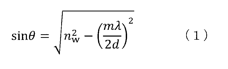
The emission angle θ of the light emitted from the waveguide element 10 into the air is expressed by the following equation (1).
式(1)からわかるように、空気中での光の波長λ、光導波層20の屈折率nwおよび光導波層20の厚さdのいずれかを変えることで光の出射方向を変えることができる。
As can be seen from the equation (1), the light emission direction is changed by changing any of the wavelength λ of the light in the air, the refractive index n w of the optical waveguide layer 20, and the thickness d of the optical waveguide layer 20. Can be done.
例えば、nw=2、d=387nm、λ=1550nm、m=1の場合、出射角度は0°である。この状態から、屈折率をnw=2.2に変化させると、出射角度は約66°に変化する。一方、屈折率を変えずに厚さをd=420nmに変化させると、出射角度は約51°に変化する。屈折率も厚さも変化させずに波長をλ=1500nmに変化させると、出射角度は約30°に変化する。このように、光の波長λ、光導波層20の屈折率nw、および光導波層20の厚さdのいずれかを変えることにより、光の出射方向を大きく変えることができる。
For example, when n w = 2, d = 387 nm, λ = 1550 nm, and m = 1, the emission angle is 0 °. From this state, when the refractive index is changed to n w = 2.2, the emission angle changes to about 66 °. On the other hand, if the thickness is changed to d = 420 nm without changing the refractive index, the emission angle changes to about 51 °. When the wavelength is changed to λ = 1500 nm without changing the refractive index and the thickness, the emission angle changes to about 30 °. In this way, by changing any of the wavelength λ of the light, the refractive index n w of the optical waveguide layer 20, and the thickness d of the optical waveguide layer 20, the light emission direction can be significantly changed.
そこで、光スキャンデバイス100は、光導波層20に入力される光の波長λ、光導波層20の屈折率nw、および光導波層20の厚さdの少なくとも1つを制御することで、光の出射方向を制御する。光の波長λは、動作中に変化させず、一定に維持されてもよい。その場合、よりシンプルな構成で光のスキャンを実現できる。波長λは、特に限定されない。例えば、波長λは、一般的なシリコン(Si)により光を吸収することで光を検出するフォトディテクタまたはイメージセンサで高い検出感度が得られる400nmから1100nm(可視光から近赤外光)の波長域に含まれ得る。他の例では、波長λは、光ファイバーまたはSi導波路において伝送損失の比較的小さい1260nmから1625nmの近赤外光の波長域に含まれ得る。なお、これらの波長範囲は一例である。使用される光の波長域は、可視光または赤外光の波長域に限定されず、例えば紫外光の波長域であってもよい。
Therefore, the optical scanning device 100 controls at least one of the wavelength λ of the light input to the optical waveguide layer 20, the refractive index n w of the optical waveguide layer 20, and the thickness d of the optical waveguide layer 20. Controls the light emission direction. The wavelength λ of light may remain constant during operation without change. In that case, light scanning can be realized with a simpler configuration. The wavelength λ is not particularly limited. For example, the wavelength λ is in the wavelength range of 400 nm to 1100 nm (visible light to near infrared light), which provides high detection sensitivity with a photodetector or image sensor that detects light by absorbing light with general silicon (Si). Can be included in. In another example, the wavelength λ can be included in the near infrared light wavelength range of 1260 nm to 1625 nm, which has a relatively low transmission loss in an optical fiber or Si waveguide. These wavelength ranges are examples. The wavelength range of the light used is not limited to the wavelength range of visible light or infrared light, and may be, for example, the wavelength range of ultraviolet light.
出射光の方向を変化させるために、光スキャンデバイス100は、各導波路素子10における光導波層20の屈折率、厚さ、および波長の少なくとも1つを変化させる第1調整素子を備え得る。
In order to change the direction of the emitted light, the optical scanning device 100 may include a first adjusting element that changes at least one of the refractive index, thickness, and wavelength of the optical waveguide layer 20 in each waveguide element 10.
以上のように、導波路素子10を用いれば、光導波層20の屈折率nw、厚さd、および波長λの少なくとも1つを変化させることで、光の出射方向を大きく変えることができる。これにより、ミラー30から出射される光の出射角度を、導波路素子10に沿った方向に変化させることができる。少なくとも1つの導波路素子10を用いることにより、このような1次元のスキャンを実現することができる。
As described above, when the waveguide element 10 is used, the light emission direction can be significantly changed by changing at least one of the refractive index n w , the thickness d, and the wavelength λ of the optical waveguide layer 20. .. As a result, the emission angle of the light emitted from the mirror 30 can be changed in the direction along the waveguide element 10. Such a one-dimensional scan can be realized by using at least one waveguide element 10.
光導波層20の少なくとも一部の屈折率を調整するために、光導波層20は、液晶材料または電気光学材料を含んでいてもよい。光導波層20は、一対の電極によって挟まれ得る。一対の電極に電圧を印加することにより、光導波層20の屈折率を変化させることができる。
In order to adjust the refractive index of at least a part of the optical waveguide layer 20, the optical waveguide layer 20 may include a liquid crystal material or an electro-optical material. The optical waveguide layer 20 may be sandwiched by a pair of electrodes. By applying a voltage to the pair of electrodes, the refractive index of the optical waveguide layer 20 can be changed.
光導波層20の厚さを調整するために、例えば、第1のミラー30および第2のミラー40の少なくとも一方に少なくとも1つのアクチュエータが接続されてもよい。少なくとも1つのアクチュエータによって第1のミラー30と第2のミラー40との距離を変化させることにより、光導波層20の厚さを変化させることができる。光導波層20が液体から形成されていれば、光導波層20の厚さは容易に変化し得る。
In order to adjust the thickness of the optical waveguide layer 20, for example, at least one actuator may be connected to at least one of the first mirror 30 and the second mirror 40. The thickness of the optical waveguide layer 20 can be changed by changing the distance between the first mirror 30 and the second mirror 40 by at least one actuator. If the optical waveguide layer 20 is formed of a liquid, the thickness of the optical waveguide layer 20 can easily change.
<2次元スキャンの動作原理>
複数の導波路素子10が一方向に配列された導波路アレイにおいて、それぞれの導波路素子10から出射される光の干渉により、光の出射方向は変化する。各導波路素子10に供給する光の位相を調整することにより、光の出射方向を変化させることができる。以下、その原理を説明する。 <Operating principle of 2D scanning>
In a waveguide array in which a plurality ofwaveguide elements 10 are arranged in one direction, the light emission direction changes due to the interference of light emitted from each waveguide element 10. By adjusting the phase of the light supplied to each waveguide element 10, the light emission direction can be changed. The principle will be described below.
複数の導波路素子10が一方向に配列された導波路アレイにおいて、それぞれの導波路素子10から出射される光の干渉により、光の出射方向は変化する。各導波路素子10に供給する光の位相を調整することにより、光の出射方向を変化させることができる。以下、その原理を説明する。 <Operating principle of 2D scanning>
In a waveguide array in which a plurality of
図3Aは、導波路アレイの出射面に垂直な方向に光を出射する導波路アレイの断面を示す図である。図3Aには、各導波路素子10を伝搬する光の位相シフト量も記載されている。ここで、位相シフト量は、左端の導波路素子10を伝搬する光の位相を基準にした値である。導波路アレイは、等間隔に配列された複数の導波路素子10を含んでいる。図3Aにおいて、破線の円弧は、各導波路素子10から出射される光の波面を示している。直線は、光の干渉によって形成される波面を示している。矢印は、導波路アレイから出射される光の方向(すなわち、波数ベクトルの方向)を示している。図3Aの例では、各導波路素子10における光導波層20を伝搬する光の位相はいずれも同じである。この場合、光は導波路素子10の配列方向(Y方向)および光導波層20が延びる方向(X方向)の両方に垂直な方向(Z方向)に出射される。
FIG. 3A is a diagram showing a cross section of a waveguide array that emits light in a direction perpendicular to the exit surface of the waveguide array. FIG. 3A also shows the amount of phase shift of the light propagating through each waveguide element 10. Here, the phase shift amount is a value based on the phase of the light propagating through the waveguide element 10 at the left end. The waveguide array includes a plurality of waveguide elements 10 arranged at equal intervals. In FIG. 3A, the broken line arc indicates the wave plane of the light emitted from each waveguide element 10. The straight line shows the wave surface formed by the interference of light. The arrows indicate the direction of the light emitted from the waveguide array (ie, the direction of the wave vector). In the example of FIG. 3A, the phases of the light propagating in the optical waveguide layer 20 in each waveguide element 10 are the same. In this case, the light is emitted in a direction (Z direction) perpendicular to both the arrangement direction (Y direction) of the waveguide element 10 and the direction (X direction) in which the optical waveguide layer 20 extends.
図3Bは、導波路アレイの出射面に垂直な方向とは異なる方向に光を出射する導波路アレイの断面を示す図である。図3Bに示す例では、複数の導波路素子10における光導波層20を伝搬する光の位相が、配列方向に一定量(Δφ)ずつ異なっている。この場合、光は、Z方向とは異なる方向に出射される。このΔφを変化させることにより、光の波数ベクトルのY方向の成分を変化させることができる。隣接する2つの導波路素子10の間の中心間距離をpとすると、光の出射角度α0は、以下の式(2)によって表される。
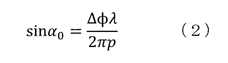
FIG. 3B is a diagram showing a cross section of a waveguide array that emits light in a direction different from the direction perpendicular to the exit surface of the waveguide array. In the example shown in FIG. 3B, the phases of the light propagating in the optical waveguide layer 20 in the plurality of waveguide elements 10 are different by a fixed amount (Δφ) in the arrangement direction. In this case, the light is emitted in a direction different from the Z direction. By changing this Δφ, the component in the Y direction of the wave number vector of light can be changed. Assuming that the distance between the centers between two adjacent waveguide elements 10 is p, the light emission angle α0 is expressed by the following equation (2).
図2に示す例では、光の出射方向は、XZ平面に平行である。すなわち、α0=0°である。図3Aおよび図3Bに示す例では、光スキャンデバイス100から出射される光の方向は、YZ平面に平行である。すなわち、θ=0°である。しかし、一般には、光スキャンデバイス100から出射される光の方向は、XZ平面にも、YZ平面にも平行ではない。すなわち、θ≠0°およびα0≠0°である。
In the example shown in FIG. 2, the light emission direction is parallel to the XZ plane. That is, α 0 = 0 °. In the examples shown in FIGS. 3A and 3B, the direction of the light emitted from the optical scanning device 100 is parallel to the YZ plane. That is, θ = 0 °. However, in general, the direction of the light emitted from the optical scanning device 100 is not parallel to the XZ plane or the YZ plane. That is, θ ≠ 0 ° and α 0 ≠ 0 °.
図4は、3次元空間における導波路アレイを模式的に示す斜視図である。図4に示す太い矢印は、光スキャンデバイス100から出射される光の方向を表す。θは、光の出射方向とYZ平面とがなす角度である。θは式(1)を満たす。α0は、光の出射方向とXZ平面とがなす角度である。α0は式(2)を満たす。
FIG. 4 is a perspective view schematically showing a waveguide array in a three-dimensional space. The thick arrow shown in FIG. 4 indicates the direction of the light emitted from the optical scanning device 100. θ is the angle formed by the light emission direction and the YZ plane. θ satisfies equation (1). α 0 is the angle formed by the light emission direction and the XZ plane. α 0 satisfies equation (2).
<導波路アレイに導入する光の位相制御>
それぞれの導波路素子10から出射される光の位相を制御するために、例えば、導波路素子10に光を導入する前段に、光の位相を変化させる位相シフタが設けられ得る。光スキャンデバイス100は、複数の導波路素子10のそれぞれに接続された複数の位相シフタと、各位相シフタを伝搬する光の位相を調整する第2調整素子とを備える。各位相シフタは、複数の導波路素子10の対応する1つにおける光導波層20に直接的にまたは他の導波路を介して繋がる導波路を含む。第2調整素子は、複数の位相シフタから複数の導波路素子10へ伝搬する光の位相の差をそれぞれ変化させることにより、複数の導波路素子10から出射される光の方向(すなわち、第3の方向D3)を変化させる。以下の説明では、導波路アレイと同様に、配列された複数の位相シフタを「位相シフタアレイ」と称することがある。 <Phase control of light introduced into waveguide array>
In order to control the phase of the light emitted from eachwaveguide element 10, for example, a phase shifter for changing the phase of the light may be provided before introducing the light into the waveguide element 10. The optical scan device 100 includes a plurality of phase shifters connected to each of the plurality of waveguide elements 10 and a second adjusting element for adjusting the phase of light propagating through each phase shifter. Each phase shifter includes a waveguide that is directly connected to the optical waveguide layer 20 in one of the plurality of waveguide elements 10 or via another waveguide. The second adjusting element changes the phase difference of the light propagating from the plurality of phase shifters to the plurality of waveguide elements 10, so that the direction of the light emitted from the plurality of waveguide elements 10 (that is, the third). The direction D3) of is changed. In the following description, a plurality of arranged phase shifters may be referred to as a "phase shifter array" as in the waveguide array.
それぞれの導波路素子10から出射される光の位相を制御するために、例えば、導波路素子10に光を導入する前段に、光の位相を変化させる位相シフタが設けられ得る。光スキャンデバイス100は、複数の導波路素子10のそれぞれに接続された複数の位相シフタと、各位相シフタを伝搬する光の位相を調整する第2調整素子とを備える。各位相シフタは、複数の導波路素子10の対応する1つにおける光導波層20に直接的にまたは他の導波路を介して繋がる導波路を含む。第2調整素子は、複数の位相シフタから複数の導波路素子10へ伝搬する光の位相の差をそれぞれ変化させることにより、複数の導波路素子10から出射される光の方向(すなわち、第3の方向D3)を変化させる。以下の説明では、導波路アレイと同様に、配列された複数の位相シフタを「位相シフタアレイ」と称することがある。 <Phase control of light introduced into waveguide array>
In order to control the phase of the light emitted from each
図5は、導波路アレイ10Aおよび位相シフタアレイ80Aを、光出射面の法線方向(Z方向)から見た模式図である。図5に示される例では、全ての位相シフタ80が同じ伝搬特性を有し、全ての導波路素子10が同じ伝搬特性を有する。それぞれの位相シフタ80およびそれぞれの導波路素子10は同じ長さであってもよいし、長さが異なっていてもよい。それぞれの位相シフタ80の長さが等しい場合は、例えば、駆動電圧によってそれぞれの位相シフト量を調整することができる。また、それぞれの位相シフタ80の長さを等ステップで変化させた構造にすることで、同じ駆動電圧で等ステップの位相シフトを与えることもできる。さらに、この光スキャンデバイス100は、複数の位相シフタ80に光を分岐して供給する光分岐器90と、各導波路素子10を駆動する第1駆動回路110と、各位相シフタ80を駆動する第2駆動回路210とをさらに備える。図5における直線の矢印は光の入力を示している。別々に設けられた第1駆動回路110と第2駆動回路210とをそれぞれ独立に制御することにより、2次元スキャンを実現できる。この例では、第1駆動回路110は、第1調整素子の1つの要素として機能し、第2駆動回路210は、第2調整素子の1つの要素として機能する。
FIG. 5 is a schematic view of the waveguide array 10A and the phase shifter array 80A as viewed from the normal direction (Z direction) of the light emitting surface. In the example shown in FIG. 5, all phase shifters 80 have the same propagation characteristics, and all waveguide elements 10 have the same propagation characteristics. Each phase shifter 80 and each waveguide element 10 may have the same length or may have different lengths. When the lengths of the respective phase shifters 80 are equal, for example, the respective phase shift amounts can be adjusted by the drive voltage. Further, by adopting a structure in which the length of each phase shifter 80 is changed in equal steps, it is possible to give the phase shift in equal steps with the same drive voltage. Further, the optical scan device 100 drives an optical turnout 90 that branches and supplies light to a plurality of phase shifters 80, a first drive circuit 110 that drives each waveguide element 10, and each phase shifter 80. A second drive circuit 210 is further provided. The straight arrow in FIG. 5 indicates the input of light. Two-dimensional scanning can be realized by independently controlling the first drive circuit 110 and the second drive circuit 210, which are provided separately. In this example, the first drive circuit 110 functions as one element of the first adjustment element, and the second drive circuit 210 functions as one element of the second adjustment element.
第1駆動回路110は、各導波路素子10における光導波層20の屈折率および厚さの少なくとも一方を変化させることにより、光導波層20から出射する光の角度を変化させる。第2駆動回路210は、各位相シフタ80における導波路20aの屈折率を変化させることにより、導波路20aの内部を伝搬する光の位相を変化させる。光分岐器90は、全反射によって光が伝搬する導波路で構成してもよいし、導波路素子10と同様の反射型導波路で構成してもよい。
The first drive circuit 110 changes the angle of light emitted from the optical waveguide layer 20 by changing at least one of the refractive index and the thickness of the optical waveguide layer 20 in each waveguide element 10. The second drive circuit 210 changes the phase of the light propagating inside the waveguide 20a by changing the refractive index of the waveguide 20a in each phase shifter 80. The optical turnout 90 may be configured by a waveguide in which light is propagated by total internal reflection, or may be configured by a reflection type waveguide similar to the waveguide element 10.
なお、光分岐器90で分岐したそれぞれの光に対して位相を制御した後に、それぞれの光を位相シフタ80に導入してもよい。この位相制御には、例えば、位相シフタ80に至るまでの導波路の長さを調整することによるパッシブな位相制御構造を用いることができる。あるいは、位相シフタ80と同様の機能を有する電気信号で制御可能な位相シフタを用いても良い。このような方法により、例えば、全ての位相シフタ80に等位相の光が供給されるように、位相シフタ80に導入される前に位相を調整してもよい。そのような調整により、第2駆動回路210による各位相シフタ80の制御をシンプルにすることができる。
After controlling the phase of each light branched by the optical turnout 90, each light may be introduced into the phase shifter 80. For this phase control, for example, a passive phase control structure by adjusting the length of the waveguide up to the phase shifter 80 can be used. Alternatively, a phase shifter that has the same function as the phase shifter 80 and can be controlled by an electric signal may be used. By such a method, for example, the phase may be adjusted before being introduced into the phase shifter 80 so that the light having the same phase is supplied to all the phase shifters 80. By such adjustment, the control of each phase shifter 80 by the second drive circuit 210 can be simplified.
上記の光スキャンデバイス100と同様の構成を有する光デバイスは、光受信デバイスとしても利用できる。光デバイスの動作原理、および動作方法などの詳細は、米国特許出願公開第2018/0224709号に開示されている。この文献の開示内容全体を本明細書に援用する。
An optical device having the same configuration as the above-mentioned optical scanning device 100 can also be used as an optical receiving device. Details such as the operating principle and operating method of the optical device are disclosed in US Patent Application Publication No. 2018/0224709. The entire disclosure of this document is incorporated herein by reference.
<貼り合わせによる光デバイスの作製>
光デバイス100は、例えば、第1のミラーを備える上部構造体および第2のミラーを備える下部構造体を貼り合わせることによって作製され得る。貼り合わせには、例えば、紫外線硬化樹脂または熱硬化樹脂などのシール部材が用いられ得る。電圧印加による光スキャンのために、光導波層20は、例えば液晶材料を含み得る。液晶材料を光デバイス100に注入するために、例えば真空封入が利用され得る。上記のシール部材によって囲まれた空間に液晶材料を注入すれば、液晶材料の注入の際に真空漏れを防ぐことができる。 <Manufacturing of optical devices by bonding>
Theoptical device 100 can be made, for example, by laminating an upper structure having a first mirror and a lower structure having a second mirror. For bonding, for example, a sealing member such as an ultraviolet curable resin or a thermosetting resin can be used. For optical scanning by applying a voltage, the optical waveguide layer 20 may include, for example, a liquid crystal material. For example, vacuum encapsulation can be used to inject the liquid crystal material into the optical device 100. If the liquid crystal material is injected into the space surrounded by the sealing member, vacuum leakage can be prevented when the liquid crystal material is injected.
光デバイス100は、例えば、第1のミラーを備える上部構造体および第2のミラーを備える下部構造体を貼り合わせることによって作製され得る。貼り合わせには、例えば、紫外線硬化樹脂または熱硬化樹脂などのシール部材が用いられ得る。電圧印加による光スキャンのために、光導波層20は、例えば液晶材料を含み得る。液晶材料を光デバイス100に注入するために、例えば真空封入が利用され得る。上記のシール部材によって囲まれた空間に液晶材料を注入すれば、液晶材料の注入の際に真空漏れを防ぐことができる。 <Manufacturing of optical devices by bonding>
The
図6は、Z方向から見たときの、光デバイス100の下部構造体100aの例を模式的に示す図である。図7Aから図7Cは、それぞれ、図6に示すA-A線断面、B-B線断面、およびC-C線断面を示す図である。図7Aから図7Cは、光デバイス100の下部構造体100aおよび上部構造体100bの例を模式的に示している。図7Aから図7Cに示す下向きの矢印は、貼り合わせの方向を表している。
FIG. 6 is a diagram schematically showing an example of the substructure 100a of the optical device 100 when viewed from the Z direction. 7A to 7C are views showing a cross section taken along line AA, a cross section taken along line BB, and a cross section taken along line CC shown in FIG. 6, respectively. 7A to 7C schematically show examples of the lower structure 100a and the upper structure 100b of the optical device 100. The downward arrows shown in FIGS. 7A to 7C indicate the bonding direction.
下部構造体100aおよび上部構造体100bを貼り合わせた後、図6に示す封入口79oから液晶材料が注入される。その後、封入口79oはシール部材79と同じ部材によって閉じられる。下部構造体100aは、基板50a、電極62a、ミラー40、誘電体層51、複数の光導波路11、複数の隔壁73、およびシール部材79を備える。上部構造体100bは、基板50b、電極62b、およびミラー30を備える。これらの詳細については、後述する。
After the lower structure 100a and the upper structure 100b are bonded together, the liquid crystal material is injected from the sealing port 79o shown in FIG. After that, the sealing port 79o is closed by the same member as the sealing member 79. The lower structure 100a includes a substrate 50a, electrodes 62a, a mirror 40, a dielectric layer 51, a plurality of optical waveguides 11, a plurality of partition walls 73, and a sealing member 79. The superstructure 100b includes a substrate 50b, electrodes 62b, and a mirror 30. Details of these will be described later.
図8Aから図8Cは、それぞれ、図7Aから図7Cに示す下部構造体100aおよび上部構造体100bを貼り合わせたときの光デバイス100の例を模式的に示す図である。図8Aから図8Cに示すように、下部構造体100aと上部構造体100bとが平行になるように貼り合わせようとしても、実際には、基板50aと基板50bとが平行にならないことがある。これは、上部構造体100bを下部構造体100aに貼り合わせる際に、上部構造体100bと下部構造体100aとが最初に接触する箇所が支点になることに起因する。例えば、シール部材79と電極62bとが接触する箇所、または、複数の隔壁73のうちの1つの隔壁とミラー30とが接触する箇所が支点になり得る。貼り合わせる際に上部構造体100bに加わる力が不均一であると、支点に近い箇所と、支点に遠い箇所とでは、基板50aと基板50bとの間隔が異なり得る。例えば、支点に遠い箇所では、支点に近い箇所よりも、基板50aと基板50bとの間隔が大きくなり得る。このため、基板50aと基板50bとが平行にならないことがある。その場合、光デバイス100から出射される光の強度、および光の出射角度が設計値からずれる可能性がある。
8A to 8C are diagrams schematically showing an example of an optical device 100 when the lower structure 100a and the upper structure 100b shown in FIGS. 7A to 7C are bonded together. As shown in FIGS. 8A to 8C, even if the lower structure 100a and the upper structure 100b are bonded so as to be parallel to each other, the substrate 50a and the substrate 50b may not actually be parallel to each other. This is because, when the upper structure 100b is attached to the lower structure 100a, the point where the upper structure 100b and the lower structure 100a first come into contact with each other becomes a fulcrum. For example, a point where the seal member 79 and the electrode 62b come into contact with each other, or a place where one of the plurality of partition walls 73 comes into contact with the mirror 30 can be a fulcrum. If the force applied to the superstructure 100b at the time of bonding is non-uniform, the distance between the substrate 50a and the substrate 50b may differ between the portion near the fulcrum and the portion far from the fulcrum. For example, at a location far from the fulcrum, the distance between the substrate 50a and the substrate 50b may be larger than at a location near the fulcrum. Therefore, the substrate 50a and the substrate 50b may not be parallel to each other. In that case, the intensity of the light emitted from the optical device 100 and the emission angle of the light may deviate from the design values.
本発明者は、以上の検討に基づき、以下の項目に記載の光デバイスに想到した。
Based on the above studies, the present inventor has come up with the optical device described in the following items.
第1の項目に係る光デバイスは、第1の方向および前記第1の方向に交差する第2の方向に沿って拡がる第1の表面を有する第1の基板と、前記第1の表面に少なくとも部分的に対向する第2の表面を有する第2の基板と、前記第1の基板と前記第2の基板との間において、前記第1の方向に沿って延びる少なくとも1つの光導波路と、前記第1の表面および前記第2の表面の少なくとも一方に配置され、第1の部分および第2の部分を含む複数の弾性スペーサと、を備える。前記第2の表面は前記第1の表面とは異なる面積を有する。前記複数の弾性スペーサの前記第1の部分は、前記第1の基板と前記第2の基板との間であって、前記第1の表面に垂直な方向から見て前記第1の基板と前記第2の基板とが重なる領域に位置する少なくとも1つの弾性スペーサである。前記複数の弾性スペーサの前記第2の部分は、前記第1の表面に垂直な方向から見て前記第1の基板と前記第2の基板とが重ならない領域に位置する少なくとも1つの弾性スペーサである。
The optical device according to the first item includes a first substrate having a first surface extending along a first direction and a second direction intersecting the first direction, and at least on the first surface. A second substrate having a second surface that is partially opposed to each other, and at least one optical waveguide extending along the first direction between the first substrate and the second substrate. A plurality of elastic spacers arranged on at least one of the first surface and the second surface and including the first portion and the second portion are provided. The second surface has a different area than the first surface. The first portion of the plurality of elastic spacers is between the first substrate and the second substrate, and the first substrate and the first substrate when viewed from a direction perpendicular to the first surface. At least one elastic spacer located in a region where the second substrate overlaps. The second portion of the plurality of elastic spacers is at least one elastic spacer located in a region where the first substrate and the second substrate do not overlap when viewed from a direction perpendicular to the first surface. is there.
この光デバイスでは、複数の弾性スペーサの第1の部分により、第1の基板と第2の基板との間隔を均一にすることができる。その結果、出射される光の強度、および出射角度の精度を大幅に改善することができる。さらに、複数の弾性スペーサの第2の部分により、第1の基板と第2の基板とが重ならない領域に設けられる構成要素を、外部の接触から保護することができる。
In this optical device, the distance between the first substrate and the second substrate can be made uniform by the first portion of the plurality of elastic spacers. As a result, the intensity of the emitted light and the accuracy of the emission angle can be significantly improved. Further, the second portion of the plurality of elastic spacers can protect the components provided in the region where the first substrate and the second substrate do not overlap from external contact.
第2の項目に係る光デバイスは、第1の項目に係る光デバイスにおいて、各々が前記第1の方向に沿って延びる複数の隔壁を更に備える。複数の隔壁は、前記第1の基板と前記第2の基板との間において前記第2の方向に並ぶ。前記複数の弾性スペーサの各々の弾性率は、前記複数の隔壁の各々の弾性率よりも小さい。
The optical device according to the second item further includes a plurality of partition walls, each of which extends along the first direction, in the optical device according to the first item. The plurality of partition walls are arranged in the second direction between the first substrate and the second substrate. The elastic modulus of each of the plurality of elastic spacers is smaller than the elastic modulus of each of the plurality of partition walls.
この光デバイスでは、バネのように作用して圧縮する弾性スペーサにより、第1の基板と第2の基板との間隔は、全体として均一になる。
In this optical device, the distance between the first substrate and the second substrate becomes uniform as a whole due to the elastic spacer that acts like a spring and compresses.
第3の項目に係る光デバイスは、第2の項目に係る光デバイスにおいて、前記複数の隔壁が、前記第1の基板と前記第2の基板とに直接的または間接的に挟持されている。前記第1の基板と前記第2の基板とによって挟持されることによる、前記第1の表面に垂直な方向における前記複数の弾性スペーサの各々の変形率は、前記垂直な方向における前記複数の隔壁の各々の変形率よりも大きい。
In the optical device according to the third item, in the optical device according to the second item, the plurality of partition walls are directly or indirectly sandwiched between the first substrate and the second substrate. The deformation rate of each of the plurality of elastic spacers in the direction perpendicular to the first surface due to being sandwiched between the first substrate and the second substrate is the deformation rate of the plurality of partition walls in the vertical direction. Greater than each deformation rate of.
この光デバイスでは、各隔壁の変形率よりも大きい各スペーサの変形率により、第1の基板と第2の基板との間隔は、全体として均一になる。
In this optical device, the distance between the first substrate and the second substrate becomes uniform as a whole due to the deformation rate of each spacer that is larger than the deformation rate of each partition wall.
第4の項目に係る光デバイスは、第1から第3の項目のいずれかに係る光デバイスにおいて、前記複数の弾性スペーサは、各々が柱状の形状を有する。
The optical device according to the fourth item is the optical device according to any one of the first to third items, and each of the plurality of elastic spacers has a columnar shape.
この光デバイスでは、第1から第3の項目に係る光デバイスと同じ効果を得ることができる。
With this optical device, the same effect as that of the optical device according to the first to third items can be obtained.
第5の項目に係る光デバイスは、第1から第4の項目のいずれかに係る光デバイスにおいて、前記少なくとも1つの光導波路の各々は、前記第1の基板と前記第2の基板との間であって、前記第1の基板と前記第2の基板とが重なる領域に配置される第1の部分と、前記第1の基板と前記第2の基板とが重ならない領域に配置される第2の部分とを備える。
The optical device according to the fifth item is the optical device according to any one of the first to fourth items, wherein each of the at least one optical waveguide is between the first substrate and the second substrate. The first portion arranged in the region where the first substrate and the second substrate overlap, and the second portion arranged in the region where the first substrate and the second substrate do not overlap. It has 2 parts.
この光デバイスでは、第2の部分から第1の部分に光を入力させることができる。
With this optical device, light can be input from the second part to the first part.
第6の項目に係る光デバイスは、第5の項目に係る光デバイスにおいて、前記少なくとも一つの光導波路は、複数の光導波路である。前記複数の弾性スペーサの前記第2の部分の少なくとも一部は、前記複数の光導波路の各々の前記第2の部分の周囲に位置している。
The optical device according to the sixth item is the optical device according to the fifth item, and the at least one optical waveguide is a plurality of optical waveguides. At least a portion of the second portion of the plurality of elastic spacers is located around the second portion of each of the plurality of optical waveguides.
この光デバイスでは、複数の弾性スペーサの第2の部分の少なくとも一部により、複数の光導波路の第2の部分を、外部の接触から保護することができる。
In this optical device, at least a part of the second part of the plurality of elastic spacers can protect the second part of the plurality of optical waveguides from external contact.
第7の項目に係る光デバイスは、第5または第6の項目に係る光デバイスにおいて、前記少なくとも一つの光導波路の各々は、隣り合う2つの隔壁の間に位置する部分を含み、前記部分において第1のグレーティングを備える。
The optical device according to the seventh item is the optical device according to the fifth or sixth item, wherein each of the at least one optical waveguide includes a portion located between two adjacent partition walls, and in the portion. It has a first grating.
この光デバイスでは、光導波路を伝搬する光は、第1のグレーティングを介して、高い効率で結合することができる。
In this optical device, the light propagating in the optical waveguide can be combined with high efficiency via the first grating.
第8の項目に係る光デバイスは、第5から第7の項目のいずれかに係る光デバイスにおいて、前記少なくとも一つの光導波路の各々は、前記第2の部分において第2のグレーティングを備える。
The optical device according to the eighth item is the optical device according to any one of the fifth to seventh items, and each of the at least one optical waveguide includes a second grating in the second part.
この光デバイスでは、第2のグレーティングを介して、外部から光導波路に光を高い効率で入力することができる。
With this optical device, light can be input to the optical waveguide from the outside with high efficiency via the second grating.
第9の項目に係る光デバイスは、第1から第8の項目のいずれかに係る光デバイスにおいて、前記第1の基板と前記第2の基板との間隔を固定するシール部材をさらに備える。前記少なくとも1つの光導波路は、1つ以上の第1の光導波路と1つ以上の第2の光導波路とがそれぞれ接続された構造を有する。前記シール部材は、前記第1の表面に垂直な方向から見たときに、前記1つ以上の第1の光導波路を囲む。
The optical device according to the ninth item further includes a sealing member for fixing the distance between the first substrate and the second substrate in the optical device according to any one of the first to eighth items. The at least one optical waveguide has a structure in which one or more first optical waveguides and one or more second optical waveguides are connected to each other. The sealing member surrounds the one or more first optical waveguides when viewed from a direction perpendicular to the first surface.
この光デバイスでは、1つ以上の第1の光導波路を、第1の基板と、第2の基板と、シール部材とによって密閉することができる。
In this optical device, one or more first optical waveguides can be sealed by a first substrate, a second substrate, and a sealing member.
第10の項目に係る光デバイスは、第9の項目に係る光デバイスにおいて、前記1つ以上の第1の光導波路が、前記第1の方向に沿って延びる1つ以上の誘電体部材をそれぞれ含む。前記第1の基板と前記第2の基板との間で且つ前記シール部材によって囲まれた領域は、前記1つ以上の誘電体部材と同じ部材によって満たされる。
The optical device according to the tenth item is the optical device according to the ninth item, wherein the one or more first optical waveguides form one or more dielectric members extending along the first direction. Including. The region between the first substrate and the second substrate and surrounded by the sealing member is filled with the same members as the one or more dielectric members.
この光デバイスでは、第1の基板と、第2の基板と、シール部材とによって密閉された空間を1つ以上の誘電体部材と同じ部材で満たすことにより、容易に1つ以上の第1の光導波路を作製することができる。
In this optical device, one or more first substrates are easily provided by filling the space sealed by the first substrate, the second substrate, and the sealing member with the same members as the one or more dielectric members. An optical waveguide can be made.
第11の項目に係る光デバイスは、第1から第10の項目のいずれかに係る光デバイスにおいて、前記1つ以上の第1の光導波路が、前記第1の方向に沿って延びる1つ以上の誘電体部材をそれぞれ含む。前記光デバイスは、前記第1の基板と前記1つ以上の誘電体部材との間、および、前記第2の基板と前記1つ以上の誘電体部材との間にそれぞれ位置する2つのミラーをさらに備える。
The optical device according to the eleventh item is the optical device according to any one of the first to tenth items, wherein the one or more first optical waveguides extend along the first direction. Includes each of the dielectric members of. The optical device has two mirrors located between the first substrate and the one or more dielectric members and between the second substrate and the one or more dielectric members. Further prepare.
この光デバイスでは、2つのミラーにより、各第1の光導波路は、反射型導波路として機能する。これにより、各第1の光導波路を伝搬する光を外部に出射させることができる。
In this optical device, each of the first optical waveguides functions as a reflective waveguide by two mirrors. As a result, the light propagating through each of the first optical waveguides can be emitted to the outside.
第12の項目に係る光デバイスは、第11の項目に係る光デバイスにおいて、前記複数の弾性スペーサの前記第1の部分の少なくとも一部が、前記2つのミラーによって挟まれた領域の外側に位置する。
The optical device according to the twelfth item is the optical device according to the eleventh item, in which at least a part of the first portion of the plurality of elastic spacers is located outside the region sandwiched by the two mirrors. To do.
この光デバイスでは、2つのミラーによって挟まれた領域の外側にパーティクルが混入しても、当該領域での第1の表面に垂直な方向における第1の基板と第2の基板との間隔が大きいことから、貼り合わせ後の第1の基板と第2の基板との間隔を均一にすることができる。
In this optical device, even if particles are mixed in the outside of the region sandwiched by the two mirrors, the distance between the first substrate and the second substrate in the direction perpendicular to the first surface in the region is large. Therefore, the distance between the first substrate and the second substrate after bonding can be made uniform.
第13の項目に係る光デバイスは、第10から第12の項目のいずれかに係る光デバイスにおいて、前記1つ以上の第1の光導波路が、前記1つ以上の誘電体部材の屈折率を調整することが可能な構造を備える。前記1つ以上の誘電体部材の屈折率を調整することにより、前記1つ以上の第1の光導波路から前記第1の基板もしくは前記第2の基板を介して出射する光の方向、または前記第1の基板もしくは前記第2の基板を介して前記1つ以上の第1の光導波路内に取り込まれる光の入射方向が変化する。
The optical device according to the thirteenth item is the optical device according to any one of the tenth to twelfth items, wherein the one or more first optical waveguides have a refractive index of the one or more dielectric members. It has a structure that can be adjusted. By adjusting the refractive index of the one or more dielectric members, the direction of light emitted from the one or more first optical waveguides through the first substrate or the second substrate, or the direction of the light. The incident direction of light taken into the one or more first optical waveguides via the first substrate or the second substrate changes.
この光デバイスでは、光の出射方向を変化させることができる光スキャンデバイス、または、光の受信方向を変化させることができる光受信デバイスを実現することができる。
With this optical device, it is possible to realize an optical scanning device capable of changing the light emitting direction or an optical receiving device capable of changing the light receiving direction.
第14の項目に係る光デバイスは、第13の項目に係る光デバイスにおいて、前記1つ以上の誘電体部材を挟む一対の電極をさらに備える。前記1つ以上の誘電体部材は、液晶材料または電気光学材料を含む。前記一対の電極に電圧を印加することにより、前記1つ以上の誘電体部材の前記屈折率が調整される。
The optical device according to the fourteenth item further includes a pair of electrodes sandwiching the one or more dielectric members in the optical device according to the thirteenth item. The one or more dielectric members include a liquid crystal material or an electro-optical material. By applying a voltage to the pair of electrodes, the refractive index of the one or more dielectric members is adjusted.
この光デバイスでは、電圧印加により、第13の項目に係る光デバイスを実現することができる。
In this optical device, the optical device according to the thirteenth item can be realized by applying a voltage.
第15の項目に係る光デバイスは、第14の項目に係る光デバイスにおいて、前記1つ以上の第1の光導波路に、それぞれ直接的にまたは他の導波路を介して繋がる1つ以上の位相シフタをさらに備える。前記1つ以上の位相シフタを通過する光の位相の差を変化させることにより、前記1つ以上の第1の光導波路から前記第1の基板もしくは前記第2の基板を介して出射する前記光の方向、または、前記第1の基板もしくは前記第2の基板を介して前記1つ以上の第1の光導波路に取り込まれる前記光の入射方向が変化する。
The optical device according to the fifteenth item is one or more phases connected to the one or more first optical waveguides, respectively, directly or via another waveguide in the optical device according to the fourteenth item. Further equipped with a shifter. The light emitted from the one or more first optical waveguides via the first substrate or the second substrate by changing the phase difference of the light passing through the one or more phase shifters. Or the incident direction of the light taken into the one or more first optical waveguides via the first substrate or the second substrate.
この光デバイスでは、1つ以上の位相シフタにより、光の出射方向を2つの方向に独立して変化させることができる光スキャンデバイス、または、光の受信方向を2つの方向に独立して変化させることができる光受信デバイスを実現することができる。
In this optical device, an optical scanning device that can independently change the light emitting direction in two directions by one or more phase shifters, or an optical scanning device that can independently change the light receiving direction in two directions. It is possible to realize an optical receiving device that can be realized.
第16の項目に係る光検出システムは、第1から第15の項目のいずれかに係る光デバイスと、前記光デバイスから出射され、対象物から反射された光を検出する光検出器と、前記光検出器の出力に基づいて、距離分布データを生成する信号処理回路と、を備える。
The optical detection system according to the sixteenth item includes an optical device according to any one of the first to fifteenth items, a photodetector that detects light emitted from the optical device and reflected from an object, and the above. It includes a signal processing circuit that generates distance distribution data based on the output of the photodetector.
この光検出システムでは、対象物から反射された光が戻ってくる時間を計測することにより、対象物の距離分布データを得ることができる。
In this light detection system, the distance distribution data of the object can be obtained by measuring the time when the light reflected from the object returns.
第17の項目に係る光デバイスの製造方法は、第1の表面を有する第1の基板と、第2の表面を有する第2の基板とを用意する工程と、前記第1の基板の前記第1の表面上に、一方向に沿って延びる少なくとも1つの光導波路を形成する工程と、前記第1の基板の前記第1の表面上、または前記第2の基板の前記第2の表面上に、複数の弾性スペーサを形成する工程と、前記複数の弾性スペーサが前記少なくとも1つの光導波路の周囲に位置するように前記第1の基板の前記第1の表面と前記第2の基板の前記第2の表面とを対向させ、前記第1の基板と前記第2の基板とを固定する工程と、前記第1の基板または前記第2の基板のうち、前記複数の弾性スペーサが設けられていない基板の一部を切断して取り除き、前記複数の弾性スペーサの一部を露出させる工程と、を含む。
The method for manufacturing an optical device according to the seventeenth item includes a step of preparing a first substrate having a first surface and a second substrate having a second surface, and the first of the first substrates. A step of forming at least one optical waveguide extending along one direction on the surface of one and on the first surface of the first substrate or on the second surface of the second substrate. A step of forming the plurality of elastic spacers, and the first surface of the first substrate and the first surface of the second substrate so that the plurality of elastic spacers are located around the at least one optical waveguide. The step of fixing the first substrate and the second substrate by facing the surfaces of the two, and the plurality of elastic spacers of the first substrate or the second substrate are not provided. A step of cutting and removing a part of the substrate to expose a part of the plurality of elastic spacers is included.
この光デバイスの製造方法では、第1の項目に係る光デバイスを製造することができる。
In this method of manufacturing an optical device, the optical device according to the first item can be manufactured.
第18の項目に係る光デバイスの製造方法は、第17の項目に係る光デバイスの製造方法において、複数の隔壁を形成する工程を更に含む。前記少なくとも1つの光導波路を形成する工程は、前記複数の隔壁を形成する工程よりも後に、前記複数の隔壁の間に1つ以上の誘電体部材を設ける工程を含む。
The method for manufacturing an optical device according to the eighteenth item further includes a step of forming a plurality of partition walls in the method for manufacturing an optical device according to the seventeenth item. The step of forming the at least one optical waveguide includes a step of providing one or more dielectric members between the plurality of partition walls after the step of forming the plurality of partition walls.
この光デバイスの製造方法では、複数の隔壁の間に1つ以上の誘電体部材をそれぞれ有する1つ以上の光導波路を形成することができる。
In this method of manufacturing an optical device, it is possible to form one or more optical waveguides each having one or more dielectric members between a plurality of partition walls.
第19の項目に係る光デバイスの製造方法は、第17の項目に係る光デバイスの製造方法において、複数の隔壁を形成する工程を更に含む。前記少なくとも1つの光導波路を形成する工程は、前記第1の基板と前記第2の基板とを固定する工程よりも後に、前記複数の隔壁の間に、液晶材料を含む1つ以上の誘電体部材を注入する工程をさらに含む。
The method for manufacturing an optical device according to the 19th item further includes a step of forming a plurality of partition walls in the method for manufacturing an optical device according to the 17th item. The step of forming the at least one optical waveguide is after the step of fixing the first substrate and the second substrate, and then one or more dielectrics including a liquid crystal material between the plurality of partition walls. It further includes the step of injecting the member.
この光デバイスの製造方法では、複数の隔壁の間に、液晶材料を含む1つ以上の誘電体部材をそれぞれ有する1つ以上の光導波路を形成することができる。
In this method of manufacturing an optical device, one or more optical waveguides each having one or more dielectric members including a liquid crystal material can be formed between a plurality of partition walls.
以下に、本開示の例示的な実施形態における光デバイスを説明する。
The optical device in the exemplary embodiment of the present disclosure will be described below.
(実施形態)
図9は、本実施形態における光デバイス100の下部構造体100aの例を模式的に示す平面図である。図10Aから図10Cは、それぞれ、図9に示すA-A線断面、B-B線断面、およびC-C線断面を示す図である。 (Embodiment)
FIG. 9 is a plan view schematically showing an example of thelower structure 100a of the optical device 100 in the present embodiment. 10A to 10C are views showing a cross section taken along line AA, a cross section taken along line BB, and a cross section taken along line CC shown in FIG. 9, respectively.
図9は、本実施形態における光デバイス100の下部構造体100aの例を模式的に示す平面図である。図10Aから図10Cは、それぞれ、図9に示すA-A線断面、B-B線断面、およびC-C線断面を示す図である。 (Embodiment)
FIG. 9 is a plan view schematically showing an example of the
光デバイス100は、第1の基板50aと、第2の基板50bと、複数の隔壁73と、複数の第1の光導波路10と、複数の弾性スペーサ77と、シール部材79と、複数の第2の光導波路11とを備える。第1の光導波路10の個数に限定はなく、1つでもよい。第2の光導波路11および弾性スペーサ77についても同様である。以下の説明では、「第1の基板50a」および「第2の基板50b」を、それぞれ「基板50a」および「基板50b」と称し、「第1の光導波路10」および「第2の光導波路11」を、それぞれ「光導波路10」および「光導波路11」と称する。
The optical device 100 includes a first substrate 50a, a second substrate 50b, a plurality of partition walls 73, a plurality of first optical waveguides 10, a plurality of elastic spacers 77, a sealing member 79, and a plurality of first substrates. The optical waveguide 11 of 2 is provided. The number of the first optical waveguides 10 is not limited, and may be one. The same applies to the second optical waveguide 11 and the elastic spacer 77. In the following description, the "first substrate 50a" and the "second substrate 50b" are referred to as the "substrate 50a" and the "substrate 50b", respectively, and the "first optical waveguide 10" and the "second optical waveguide 10" are referred to. "11" are referred to as "optical waveguide 10" and "optical waveguide 11", respectively.
本実施形態における光デバイス100は、下部構造体100aと、上部構造体100bとを備える。
The optical device 100 in this embodiment includes a lower structure 100a and an upper structure 100b.
下部構造体100aは、基板50aと、電極62aと、ミラー40と、誘電体層51と、複数の隔壁73と、複数の弾性スペーサ77と、シール部材79と、光導波路11とを備える。図10Aに示すように、基板50aは、X方向およびY方向に沿って拡がる第1の表面50asを有する。基板50a上には、電極62aが設けられている。電極62a上には、ミラー40が設けられている。ミラー40上には、誘電体層51が設けられている。誘電体層51上には、隔壁73と、弾性スペーサ77と、シール部材79と、光導波路11とが設けられている。
The lower structure 100a includes a substrate 50a, electrodes 62a, a mirror 40, a dielectric layer 51, a plurality of partition walls 73, a plurality of elastic spacers 77, a sealing member 79, and an optical waveguide 11. As shown in FIG. 10A, the substrate 50a has a first surface 50as that extends along the X and Y directions. An electrode 62a is provided on the substrate 50a. A mirror 40 is provided on the electrode 62a. A dielectric layer 51 is provided on the mirror 40. A partition wall 73, an elastic spacer 77, a sealing member 79, and an optical waveguide 11 are provided on the dielectric layer 51.
上部構造体100bは、第2の表面50bsを有する基板50bと、電極62bと、ミラー40とを備える。第2の表面50bsは、基板50aの第1の表面50asに対向する。第2の表面50bsは、第1の表面50asと略同じ面積を有する。基板50b上には、電極62bが設けられている。電極62b上には、ミラー30が設けられている。
The upper structure 100b includes a substrate 50b having a second surface 50bs, an electrode 62b, and a mirror 40. The second surface 50bs faces the first surface 50as of the substrate 50a. The second surface 50bs has substantially the same area as the first surface 50as. An electrode 62b is provided on the substrate 50b. A mirror 30 is provided on the electrode 62b.
基板50aおよび基板50bのうち、光が出射される側の基板は、透光性を有する。基板50aおよび基板50bの両方が、透光性を有していてもよい。同様に、電極62aおよび電極62bのうち、光が出射される側の電極は、透光性を有する。電極62aおよび電極62bの両方が、透光性を有していてもよい。電極62aおよび電極62bの少なくとも一方は、例えば、透明電極から形成され得る。図9、および図10Aから図10Cに示す例では、上部構造体100bの電極62bおよび基板50bを介して、光導波路10から光が出射される。
Of the substrate 50a and the substrate 50b, the substrate on which light is emitted has translucency. Both the substrate 50a and the substrate 50b may have translucency. Similarly, of the electrodes 62a and 62b, the electrode on which light is emitted has translucency. Both the electrode 62a and the electrode 62b may have translucency. At least one of the electrode 62a and the electrode 62b can be formed from, for example, a transparent electrode. In the examples shown in FIGS. 9 and 10A to 10C, light is emitted from the optical waveguide 10 via the electrodes 62b and the substrate 50b of the superstructure 100b.
図9に示すように、複数の隔壁73は、基板50aと基板50bとの間に位置し、Y方向に並んでいる。各隔壁73は、X方向に沿って延びる。
As shown in FIG. 9, the plurality of partition walls 73 are located between the substrate 50a and the substrate 50b and are arranged in the Y direction. Each partition 73 extends along the X direction.
複数の光導波路10は、複数の隔壁73の間に規定される。各光導波路10は、X方向に沿って延びる誘電体部材21を含む。なお、図10Aから10Cは、誘電体部材21を構成する材料が注入される前の状態を示している。誘電体部材21は、例えば、液晶材料または電気光学材料を含む。光導波路10は、ミラー30と、ミラー40と、誘電体部材21とを備える。誘電体部材21は、ミラー30、40、および隣接する2つの隔壁73によって囲まれた領域に設けられる。光導波路10は、前述のスローライト導波路として機能する。ミラー40は、基板50aと誘電体部材21との間に位置する。ミラー30は、基板50bと誘電体部材21との間に位置する。誘電体部材21は、図2に示す光導波層20を構成する。図9、および図10Aから図10Cに示す例では、光導波層20内の誘電体層51の一部が除去され、ミラー40の一部が露出している。光導波層20は、ミラー30とミラー40とによって挟まれた領域に形成される。
The plurality of optical waveguides 10 are defined between the plurality of partition walls 73. Each optical waveguide 10 includes a dielectric member 21 extending along the X direction. In addition, FIGS. 10A to 10C show the state before the material constituting the dielectric member 21 is injected. The dielectric member 21 includes, for example, a liquid crystal material or an electro-optical material. The optical waveguide 10 includes a mirror 30, a mirror 40, and a dielectric member 21. The dielectric member 21 is provided in a region surrounded by mirrors 30, 40 and two adjacent partition walls 73. The optical waveguide 10 functions as the slow light waveguide described above. The mirror 40 is located between the substrate 50a and the dielectric member 21. The mirror 30 is located between the substrate 50b and the dielectric member 21. The dielectric member 21 constitutes the optical waveguide layer 20 shown in FIG. In the examples shown in FIGS. 9 and 10A to 10C, a part of the dielectric layer 51 in the optical waveguide layer 20 is removed, and a part of the mirror 40 is exposed. The optical waveguide layer 20 is formed in a region sandwiched between the mirror 30 and the mirror 40.
誘電体部材21の屈折率は、隔壁73および誘電体層51の屈折率よりも高い。これにより、光導波層20内を伝搬する光は、隔壁73およびその直下の誘電体層51に漏れることはない。光導波層20内を伝搬する光は、光導波層20と各隔壁73との界面、および、光導波層20と誘電体層51との界面では全反射される。
The refractive index of the dielectric member 21 is higher than the refractive index of the partition wall 73 and the dielectric layer 51. As a result, the light propagating in the optical waveguide layer 20 does not leak to the partition wall 73 and the dielectric layer 51 immediately below the partition wall 73. The light propagating in the optical waveguide layer 20 is totally reflected at the interface between the optical waveguide layer 20 and each partition wall 73 and at the interface between the optical waveguide layer 20 and the dielectric layer 51.
一対の電極62aおよび電極62bは、誘電体部材21を直接的または間接的に挟む。「直接的に挟む」とは、他の部材を介することなく挟むことを意味する。「間接的に挟む」とは、他の部材を介して挟むことを意味する。一対の電極62aおよび電極62bに電圧を印加することにより、誘電体部材21の屈折率が調整される。その結果、光導波路10から外部に出射される光の出射角度が変化する。
The pair of electrodes 62a and 62b directly or indirectly sandwich the dielectric member 21. "Directly sandwiching" means sandwiching without interposing other members. "Indirectly sandwiching" means sandwiching through another member. By applying a voltage to the pair of electrodes 62a and 62b, the refractive index of the dielectric member 21 is adjusted. As a result, the emission angle of the light emitted to the outside from the optical waveguide 10 changes.
なお、光導波路10は、スローライト導波路である必要はない。光導波路10は、例えば、全反射によって光を伝搬させる導波路であってもよい。当該導波路では、基板50aまたは基板50bを介してではなく、光導波路10の端部から、光が外部に出射される。
The optical waveguide 10 does not have to be a slow light waveguide. The optical waveguide 10 may be, for example, a waveguide that propagates light by total internal reflection. In the waveguide, light is emitted to the outside not through the substrate 50a or the substrate 50b but from the end of the optical waveguide 10.
複数の弾性スペーサ77は、複数の光導波路10の周囲に位置する。図9に示す例では、複数の柱状の弾性スペーサ77が2次元的に配置されている。この配置は、規則的または周期的であってもよいし、不規則的であってもよい。XY平面内の弾性スペーサ77の直径は、例えば、10μm以上100μm以下であり得る。図9に示す例では、弾性スペーサ77は、シール部材79によって囲まれた領域の内側および外側の両方に位置する。弾性スペーサ77は、当該領域の内側および外側の一方にのみ設けられていてもよい。このように、弾性スペーサ77は、当該領域の内側および外側の少なくとも一方に位置する。一部の弾性スペーサ77が、光導波層20内に設けられてもよい。弾性スペーサ77は、シール部材79によって囲まれた領域の内側および/または外側において、1つの繋がった形状を有していてもよい。当該形状は、例えば、Z方向から見た場合に、直線状、曲線状、波線状、またはジグザグ線状の形状であり得る。
The plurality of elastic spacers 77 are located around the plurality of optical waveguides 10. In the example shown in FIG. 9, a plurality of columnar elastic spacers 77 are two-dimensionally arranged. This arrangement may be regular, periodic, or irregular. The diameter of the elastic spacer 77 in the XY plane can be, for example, 10 μm or more and 100 μm or less. In the example shown in FIG. 9, the elastic spacer 77 is located both inside and outside the area surrounded by the sealing member 79. The elastic spacer 77 may be provided only on one of the inner side and the outer side of the region. As described above, the elastic spacer 77 is located at least one of the inside and the outside of the region. A part of the elastic spacer 77 may be provided in the optical waveguide layer 20. The elastic spacer 77 may have one connected shape inside and / or outside the area surrounded by the sealing member 79. The shape can be, for example, a linear, curved, wavy, or zigzag linear shape when viewed from the Z direction.
下部構造体100aおよび上部構造体100bを貼り合わせる前の状態では、Z方向における弾性スペーサ77の寸法は、Z方向における隔壁73およびミラー30の寸法の合計よりも大きい。また、その状態では、Z方向における弾性スペーサ77の寸法は、Z方向におけるシール部材79の寸法よりも大きい。したがって、下部構造体100aおよび上部構造体100bを貼り付ける際、上部構造体100bの電極62bは、下部構造体100aの弾性スペーサ77に最初に接触する。このため、シール部材79と電極62bとが接触する箇所、または、隔壁73とミラー30とが接触する箇所が支点になることはない。
In the state before the lower structure 100a and the upper structure 100b are bonded together, the size of the elastic spacer 77 in the Z direction is larger than the total size of the partition wall 73 and the mirror 30 in the Z direction. Further, in that state, the size of the elastic spacer 77 in the Z direction is larger than the size of the seal member 79 in the Z direction. Therefore, when the lower structure 100a and the upper structure 100b are attached, the electrode 62b of the upper structure 100b first contacts the elastic spacer 77 of the lower structure 100a. Therefore, the point where the seal member 79 and the electrode 62b come into contact with each other or the part where the partition wall 73 and the mirror 30 come into contact with each other does not serve as a fulcrum.
弾性スペーサ77では、弾性変形が生じる。弾性体に力を加えてひずみが生じた場合、弾性率は、加えた力を生じたひずみで割ることによって定義される。弾性スペーサ77の弾性率は、隔壁73およびミラー30の弾性率よりも小さい。すなわち、弾性スペーサ77は、隔壁73およびミラー30よりも変形しやすい。下部構造体100aおよび上部構造体100bを貼り合わせたときに、弾性スペーサ77はバネのように作用して圧縮する。これにより、隔壁73の上面とミラー30の反射面とが均一に接触して、基板50aと基板50bとの間隔が全体として均一になる。その結果、基板50aと基板50bとがほぼ平行になる。このとき、基板50aと基板50bとによって挟持されることによる、Z方向における各弾性スペーサの変形率は、Z方向における各隔壁の変形率よりも大きい。
Elastic deformation occurs in the elastic spacer 77. When a force is applied to an elastic body to cause strain, the elastic modulus is defined by dividing the applied force by the generated strain. The elastic modulus of the elastic spacer 77 is smaller than the elastic modulus of the partition wall 73 and the mirror 30. That is, the elastic spacer 77 is more easily deformed than the partition wall 73 and the mirror 30. When the lower structure 100a and the upper structure 100b are bonded together, the elastic spacer 77 acts like a spring and compresses. As a result, the upper surface of the partition wall 73 and the reflective surface of the mirror 30 come into uniform contact with each other, and the distance between the substrate 50a and the substrate 50b becomes uniform as a whole. As a result, the substrate 50a and the substrate 50b become substantially parallel. At this time, the deformation rate of each elastic spacer in the Z direction due to being sandwiched between the substrate 50a and the substrate 50b is larger than the deformation rate of each partition wall in the Z direction.
シール部材79は、基板50aと基板50bとの間隔を固定する。図9に示すように、シール部材79は、Z方向から見たときに、複数の光導波路10および複数の隔壁73を囲む。シール部材79は、Y方向において、光導波路11を跨ぐように設けられている。シール部材79の上面は、XY平面に平行である。誘電体層51上でのZ方向におけるシール部材79の寸法は、Z方向における隔壁73の寸法およびミラー30の寸法の合計と同じか、当該合計よりも大きい。シール部材79は、例えば、紫外線硬化樹脂または熱硬化樹脂から形成され得る。基板50aと基板50bとの間隔を長期間維持できる部材であれば、シール部材79の材料は、紫外線硬化樹脂または熱硬化樹脂である必要はない。
The seal member 79 fixes the distance between the substrate 50a and the substrate 50b. As shown in FIG. 9, the seal member 79 surrounds the plurality of optical waveguides 10 and the plurality of partition walls 73 when viewed from the Z direction. The seal member 79 is provided so as to straddle the optical waveguide 11 in the Y direction. The upper surface of the seal member 79 is parallel to the XY plane. The dimensions of the sealing member 79 in the Z direction on the dielectric layer 51 are the same as or larger than the sum of the dimensions of the partition wall 73 and the mirror 30 in the Z direction. The seal member 79 can be formed from, for example, an ultraviolet curable resin or a thermosetting resin. The material of the sealing member 79 does not need to be an ultraviolet curable resin or a thermosetting resin as long as the distance between the substrate 50a and the substrate 50b can be maintained for a long period of time.
光導波路11は、光導波路10に接続されている。光導波路11から光導波路10に光が供給される。図9、および図10Aから図10Cに示す例では、光導波路11は、誘電体層51上に位置する。誘電体層51は、基板50aと光導波路11との間に位置する。Z方向における誘電体層51の寸法を調整することにより、光導波路11を伝搬する光を、高い効率で光導波路10に結合させることができる。Z方向における誘電体層51の寸法は、例えば、光導波路11がZ方向における光導波層20の中央付近に位置するように調整され得る。光導波路11は、全反射によって光を伝搬させる導波路である。そのため、光導波路11の屈折率は、誘電体層51の屈折率よりも高い。なお、光導波路11は、スローライト導波路であってもよい。
The optical waveguide 11 is connected to the optical waveguide 10. Light is supplied from the optical waveguide 11 to the optical waveguide 10. In the examples shown in FIGS. 9 and 10A to 10C, the optical waveguide 11 is located on the dielectric layer 51. The dielectric layer 51 is located between the substrate 50a and the optical waveguide 11. By adjusting the dimensions of the dielectric layer 51 in the Z direction, the light propagating in the optical waveguide 11 can be coupled to the optical waveguide 10 with high efficiency. The dimensions of the dielectric layer 51 in the Z direction can be adjusted, for example, so that the optical waveguide 11 is located near the center of the optical waveguide 11 in the Z direction. The optical waveguide 11 is a waveguide that propagates light by total reflection. Therefore, the refractive index of the optical waveguide 11 is higher than that of the dielectric layer 51. The optical waveguide 11 may be a slow light waveguide.
複数の光導波路11の各々は、複数の隔壁73のうち隣り合う2つの隔壁の間に位置する部分を備える。図9から図10Cに示されるように、複数の光導波路11の各々は、当該部分においてグレーティング15を備えていてもよい。光導波路11の伝搬定数は、光導波路10の伝搬定数とは異なる。グレーティング15により、光導波路11の伝搬定数は、逆格子分だけシフトする。逆格子分だけシフトした光導波路11の伝搬定数が、光導波路10の伝搬定数と一致するとき、光導波路11を伝搬する光は、高効率で光導波路10に結合する。
Each of the plurality of optical waveguides 11 includes a portion of the plurality of partition walls 73 located between two adjacent partition walls. As shown in FIGS. 9 to 10C, each of the plurality of optical waveguides 11 may include a grating 15 at the portion. The propagation constant of the optical waveguide 11 is different from the propagation constant of the optical waveguide 10. Due to the grating 15, the propagation constant of the optical waveguide 11 is shifted by the reciprocal lattice. When the propagation constant of the optical waveguide 11 shifted by the reciprocal lattice matches the propagation constant of the optical waveguide 10, the light propagating through the optical waveguide 11 is coupled to the optical waveguide 10 with high efficiency.
図11Aから図11Cは、それぞれ、図10Aから図10Cに示す下部構造体100aおよび上部構造体100bを貼り合わせた状態における光デバイス100の例を模式的に示す図である。図11Aから図11Cに示すように、基板50aと基板50bとを貼り合わせると、弾性スペーサ77を介して、対向する第1の表面50asおよび第2の表面50bsに均一に力が加わる。これにより、基板50aと基板50bとが実質的に平行になる。弾性スペーサ77は、基板50aと基板50bとによって直接的または間接的に挟持される。図11Aから図11Cに示す例では、弾性スペーサ77は、下部構造体100aの誘電体層51と、上部構造体100bの電極62bとによって直接的に挟持される。Z方向における弾性スペーサ77の寸法は、Z方向における隔壁73の寸法よりも大きい。
11A to 11C are diagrams schematically showing an example of an optical device 100 in a state where the lower structure 100a and the upper structure 100b shown in FIGS. 10A to 10C are bonded together. As shown in FIGS. 11A to 11C, when the substrate 50a and the substrate 50b are bonded together, a force is uniformly applied to the first surface 50as and the second surface 50bs facing each other via the elastic spacer 77. As a result, the substrate 50a and the substrate 50b become substantially parallel. The elastic spacer 77 is directly or indirectly sandwiched between the substrate 50a and the substrate 50b. In the example shown in FIGS. 11A to 11C, the elastic spacer 77 is directly sandwiched between the dielectric layer 51 of the lower structure 100a and the electrode 62b of the upper structure 100b. The size of the elastic spacer 77 in the Z direction is larger than the size of the partition wall 73 in the Z direction.
図12Aおよび図12Bは、それぞれ、図11Aおよび図11Bに示す基板50bおよび電極62bの一部が切断された例を模式的に示す図である。切断により、シール部材79によって囲まれた領域の周辺の一部が取り除かれる。その結果、第2の表面50bsは、第1の表面50asとは異なる面積を有する。図12Aおよび図12Bに示すように、光導波路11は、Z方向から見たとき、基板50aとは重なるが、基板50bとは重ならない部分を含む。光導波路11は、当該重ならない部分において、グレーティング13を備えていてもよい。上記の理由と同様の理由から、グレーティング13を介して光を入力した場合、入力された光は、より高い効率で光導波路11に結合させることができる。光導波路11は、基板50bとは重なり、基板50aとは重ならない部分を含んでいてもよいし、基板50aおよび基板50bの両方と重ならない部分を含んでいてもよい。このように、光導波路11は、各基板の表面に垂直な方向から見た場合に、基板50aおよび基板50bの少なくとも一方と重ならない部分を備え得る。その場合、一部の弾性スペーサ77は、基板50aおよび基板50bに狭持されずに、誘電体層51上に残る。当該一部の弾性スペーサ77のZ方向における寸法は、残りの弾性スペーサ77のZ方向における寸法よりも大きい。当該一部の弾性スペーサ77が残存することにより、電極62aまたは電極62b、グレーティング13、および、光導波路11を外部の接触から保護することができる。
12A and 12B are diagrams schematically showing an example in which a part of the substrate 50b and the electrode 62b shown in FIGS. 11A and 11B are cut off, respectively. By cutting, a part around the area surrounded by the sealing member 79 is removed. As a result, the second surface 50bs has an area different from that of the first surface 50as. As shown in FIGS. 12A and 12B, the optical waveguide 11 includes a portion that overlaps with the substrate 50a but does not overlap with the substrate 50b when viewed from the Z direction. The optical waveguide 11 may include a grating 13 at the non-overlapping portion. For the same reason as described above, when light is input via the grating 13, the input light can be coupled to the optical waveguide 11 with higher efficiency. The optical waveguide 11 may include a portion that overlaps with the substrate 50b and does not overlap with the substrate 50a, or may include a portion that does not overlap with both the substrate 50a and the substrate 50b. As described above, the optical waveguide 11 may include a portion that does not overlap with at least one of the substrate 50a and the substrate 50b when viewed from a direction perpendicular to the surface of each substrate. In that case, a part of the elastic spacer 77 remains on the dielectric layer 51 without being sandwiched between the substrates 50a and the substrate 50b. The dimensions of some of the elastic spacers 77 in the Z direction are larger than the dimensions of the remaining elastic spacers 77 in the Z direction. The remaining elastic spacer 77 can protect the electrode 62a or the electrode 62b, the grating 13, and the optical waveguide 11 from external contact.
弾性スペーサ77の役割をまとめると以下のようになる。弾性スペーサ77は、光デバイス100の製造時には、基板50aおよび基板50bを平行にする役割を果たす。弾性スペーサ77は、光デバイス100の使用時には、一部の構成要素を外部の接触から保護する役割を果たす。
The roles of the elastic spacer 77 can be summarized as follows. The elastic spacer 77 serves to make the substrate 50a and the substrate 50b parallel to each other during the manufacture of the optical device 100. The elastic spacer 77 serves to protect some components from external contact when using the optical device 100.
誘電体部材21が液晶材料によって構成される場合、下部構造体100aおよび上部構造体100bを貼り合わせた後、封入口79oから、液晶材料が注入される。これらの貼り合わせた構造体の少なくとも一方の一部を切断した後、封入口79oから、液晶材料を注入してもよい。液晶材料の注入後、封入口79oは、シール部材79と同じ部材によって閉じられる。このようにして密閉された領域は、全体的に液晶材料によって満たされる。当該領域は、基板50aと基板50bとの間に位置し、シール部材79によって囲まれた領域である。当該領域は、誘電体部材21と同じ部材によって満たされる。
When the dielectric member 21 is made of a liquid crystal material, the liquid crystal material is injected from the sealing port 79o after the lower structure 100a and the upper structure 100b are bonded together. After cutting at least one part of these bonded structures, the liquid crystal material may be injected from the sealing port 79o. After injection of the liquid crystal material, the sealing port 79o is closed by the same member as the sealing member 79. The area sealed in this way is entirely filled with the liquid crystal material. The region is located between the substrate 50a and the substrate 50b and is surrounded by the sealing member 79. The region is filled with the same members as the dielectric member 21.
以下に、光デバイス100の作製に用いられる構成要素の材料および寸法の詳細な例を説明する。以下、Z方向における寸法を「厚さ」と称することがある。
A detailed example of the materials and dimensions of the components used in the fabrication of the optical device 100 will be described below. Hereinafter, the dimension in the Z direction may be referred to as "thickness".
まず、下部構造体100aの構成要素の材料および寸法の例を説明する。
First, an example of the material and dimensions of the constituent elements of the lower structure 100a will be described.
基板50aは、例えばSiO2層から形成され得る。X方向およびY方向における基板50aの寸法は、例えば両方とも15mmであり得る。基板50aの厚さは、例えば0.7mmであり得る。
The substrate 50a can be formed from, for example, two SiO layers. The dimensions of the substrate 50a in the X and Y directions can be, for example, both 15 mm. The thickness of the substrate 50a can be, for example, 0.7 mm.
電極62aは、例えばITOスパッタ層から形成され得る。電極62aの厚さは、例えば50nmであり得る。
The electrode 62a can be formed from, for example, an ITO sputtered layer. The thickness of the electrode 62a can be, for example, 50 nm.
ミラー40は、多層反射膜であり得る。多層反射膜は、例えばNb2O5層とSiO2層とを交互に蒸着して積層することによって形成され得る。Nb2O5層は、屈折率n=2.282を有する。Nb2O5層の厚さは、例えば100nm程度であり得る。SiO2層は、屈折率n=1.468を有する。SiO2層の厚さは、例えば200nm程度であり得る。ミラー40は、例えば31層のNb2O5層、および30層のSiO2層の合計61層を有する。ミラー40の厚さは、例えば9.1μmであり得る。
The mirror 40 can be a multilayer reflective film. The multilayer reflective film can be formed, for example, by alternately depositing and laminating Nb 2 O 5 layers and SiO 2 layers. The Nb 2 O 5 layer has a refractive index n = 2.282. The thickness of the Nb 2 O 5 layer can be, for example, about 100 nm. The SiO 2 layer has a refractive index n = 1.468. The thickness of the SiO 2 layer can be, for example, about 200 nm. The mirror 40 has, for example, 31 layers of Nb 2 O 5 layers and 30 layers of SiO 2 layers for a total of 61 layers. The thickness of the mirror 40 can be, for example, 9.1 μm.
誘電体層51は、例えばSiO2蒸着層から形成され得る。SiO2蒸着層は、屈折率n=1.468を有する。SiO2蒸着層の厚さは、例えば1.0μm程度であり得る。
The dielectric layer 51 can be formed from, for example, a SiO 2 vapor deposition layer. The SiO 2 thin-film deposition layer has a refractive index of n = 1.468. The thickness of the SiO 2 thin-film deposition layer can be, for example, about 1.0 μm.
光導波路11は、例えばNb2O5蒸着層から形成され得る。Nb2O5蒸着層は、屈折率n=2.282を有する。Nb2O5蒸着層の厚さは、例えば300nm程度であり得る。光導波路11には、グレーティング15およびグレーティング13が形成され得る。グレーティング15は、例えばデューティ比1:1、およびピッチ640nmを有する。グレーティング13は、例えばデューティ比1:1、およびピッチ680nmを有する。グレーティング15およびグレーティング13は、フォトリソグラフィ法によるパターニングによって形成され得る。Y方向における光導波路11の寸法は、例えば10μmであり得る。
The optical waveguide 11 can be formed from, for example, an Nb 2 O 5 vapor deposition layer. The Nb 2 O 5 thin-film deposition layer has a refractive index of n = 2.282. The thickness of the Nb 2 O 5 thin-film deposition layer can be, for example, about 300 nm. A grating 15 and a grating 13 may be formed on the optical waveguide 11. The grating 15 has, for example, a duty ratio of 1: 1 and a pitch of 640 nm. The grating 13 has, for example, a duty ratio of 1: 1 and a pitch of 680 nm. The grating 15 and the grating 13 can be formed by patterning by a photolithography method. The size of the optical waveguide 11 in the Y direction can be, for example, 10 μm.
隔壁73は、SiO2蒸着層から形成され得る。SiO2蒸着層は、屈折率n=1.468を有する。SiO2蒸着層の厚さは、例えば1.0μmであり得る。Y方向における隔壁73の寸法は、例えば50μmであり得る。
The partition wall 73 may be formed from a SiO 2 vapor deposition layer. The SiO 2 thin-film deposition layer has a refractive index of n = 1.468. The thickness of the SiO 2 thin-film deposition layer can be, for example, 1.0 μm. The size of the partition wall 73 in the Y direction can be, for example, 50 μm.
光導波層20内において、誘電体層51の一部は、例えばフォトリソグラフィ法によるパターニングによって除去され得る。光導波層20の厚さは、例えば2.0μmであり得る。Y方向における光導波層20の寸法は、例えば10μmであり得る。
In the optical waveguide layer 20, a part of the dielectric layer 51 can be removed by patterning by, for example, a photolithography method. The thickness of the optical waveguide layer 20 can be, for example, 2.0 μm. The size of the optical waveguide layer 20 in the Y direction can be, for example, 10 μm.
次に、上部構造体100bの構成要素の材料および寸法の詳細を説明する。
Next, the details of the materials and dimensions of the components of the superstructure 100b will be described.
基板50bは、例えばSiO2層から形成され得る。X方向およびY方向における基板50aの寸法は、例えばそれぞれ8mmおよび20mmであり、基板50aの厚さは、例えば0.7mmであり得る。
The substrate 50b can be formed from, for example, two SiO layers. The dimensions of the substrate 50a in the X and Y directions can be, for example, 8 mm and 20 mm, respectively, and the thickness of the substrate 50a can be, for example, 0.7 mm.
電極62bは、例えばITOスパッタ層から形成され得る。電極62bの厚さは、例えば50nmであり得る。
The electrode 62b can be formed from, for example, an ITO sputtered layer. The thickness of the electrode 62b can be, for example, 50 nm.
ミラー30は、多層反射膜であり得る。多層反射膜は、Nb2O5層とSiO2層とを交互に蒸着して積層することによって形成され得る。Nb2O5層は、屈折率n=2.282を有する。Nb2O5層の厚さは、例えば100nm程度であり得る。SiO2層は、屈折率n=1.468を有する。SiO2層の厚さは、例えば200nm程度であり得る。ミラー30は、例えば7層のNb2O5層、および6層のSiO2層の合計13層を有する。ミラー30の厚さは、例えば1.9μmであり得る。
The mirror 30 can be a multilayer reflective film. The multilayer reflective film can be formed by alternately depositing and laminating Nb 2 O 5 layers and SiO 2 layers. The Nb 2 O 5 layer has a refractive index n = 2.282. The thickness of the Nb 2 O 5 layer can be, for example, about 100 nm. The SiO 2 layer has a refractive index n = 1.468. The thickness of the SiO 2 layer can be, for example, about 200 nm. The mirror 30 has, for example, 7 layers of Nb 2 O 5 layers and 6 layers of SiO 2 layers for a total of 13 layers. The thickness of the mirror 30 can be, for example, 1.9 μm.
次に、弾性スペーサ77およびシール部材79の材料および寸法の詳細な例を説明する。
Next, detailed examples of the materials and dimensions of the elastic spacer 77 and the sealing member 79 will be described.
弾性スペーサ77には、例えば積水化学製のミクロパールEX-003が用いられ得る。下部構造体100aおよび上部構造体100bを貼り合わせる前の状態において、Z方向における弾性スペーサ77の寸法は、例えば3.0μmである。弾性スペーサ77の当該寸法は、隔壁73の厚さおよびミラー30の厚さの合計よりも大きい。隔壁73の厚さは、例えば1μm、ミラー30の厚さは、例えば1.9μmであり得る。
For the elastic spacer 77, for example, Micropearl EX-003 manufactured by Sekisui Chemical can be used. In the state before the lower structure 100a and the upper structure 100b are bonded together, the size of the elastic spacer 77 in the Z direction is, for example, 3.0 μm. The dimension of the elastic spacer 77 is larger than the sum of the thickness of the partition wall 73 and the thickness of the mirror 30. The thickness of the partition wall 73 may be, for example, 1 μm, and the thickness of the mirror 30 may be, for example, 1.9 μm.
誘電体部材21には、例えば5CB液晶が用いられ得る。
For the dielectric member 21, for example, a 5CB liquid crystal can be used.
シール部材79には、例えばスリーボンド製の紫外線硬化接着剤3026Eが用いられ得る。例えば、波長365nmおよびエネルギー密度100mJ/cm2の紫外線照射によってシール部材79を硬化することにより、下部構造体100aおよび上部構造体100bを貼り合わせることができる。これにより、本実施形態における光デバイス100が得られる。
For the sealing member 79, for example, UV curable adhesive 3026E manufactured by ThreeBond can be used. For example, the lower structure 100a and the upper structure 100b can be bonded together by curing the seal member 79 by irradiation with ultraviolet rays having a wavelength of 365 nm and an energy density of 100 mJ / cm 2 . As a result, the optical device 100 according to the present embodiment is obtained.
なお、基板50aおよび基板50bは、SiO2から形成されなくてもよい。基板50aおよび基板50bは、例えば、ガラスもしくはサファイアなどの無機基板、または、アクリルもしくはポリカーボネートなどの樹脂基板であってもよい。これらの無機基板および樹脂基板は、透光性を有する。
The substrate 50a and the substrate 50b do not have to be formed of SiO 2 . The substrate 50a and the substrate 50b may be, for example, an inorganic substrate such as glass or sapphire, or a resin substrate such as acrylic or polycarbonate. These inorganic substrates and resin substrates have translucency.
光が出射されるミラー30の透過率は、例えば99.9%であり、光が出射されないミラー40の透過率は、例えば99.99%である。この条件は、多層反射膜の層数の調整によって実現することができる。多層反射膜内の2つの層の組み合わせとして、例えば、一方の層の屈折率は2以上であり、他方の層の屈折率は2未満である。2つの屈折率の差が大きければ、高い反射率を得ることできる。屈折率が2以上の層は、例えば、SiNx、AlNx、TiOx、ZrOx、NbOx、およびTaOxからなる群から選択される少なくとも1つから形成され得る。屈折率が2未満の層は、例えば、SiOxまたはAlOxからなる群から選択される少なくとも1つから形成され得る。
The transmittance of the mirror 30 from which light is emitted is, for example, 99.9%, and the transmittance of the mirror 40 from which light is not emitted is, for example, 99.99%. This condition can be realized by adjusting the number of layers of the multilayer reflective film. As a combination of the two layers in the multilayer reflective film, for example, one layer has a refractive index of 2 or more and the other layer has a refractive index of less than 2. If the difference between the two refractive indexes is large, a high reflectance can be obtained. The layer having a refractive index of 2 or more can be formed from at least one selected from the group consisting of, for example, SiN x , AlN x , TiO x , ZrO x , NbO x , and TaO x . The layer having a refractive index of less than 2 can be formed from, for example, at least one selected from the group consisting of SiO x or AlO x .
誘電体層51の屈折率は、例えば2未満であり、光導波路11の屈折率は例えば2以上である。2つの屈折率の差が大きければ、光導波路11から誘電体層51に染み出すエバネッセント光を減らすことができる。
The refractive index of the dielectric layer 51 is, for example, less than 2, and the refractive index of the optical waveguide 11 is, for example, 2 or more. If the difference between the two refractive indexes is large, the evanescent light exuding from the optical waveguide 11 to the dielectric layer 51 can be reduced.
次に、図9に示すaからiの箇所、およびαからδの箇所での間隔を測定した結果を説明する。当該間隔は、リタデーション測定によって調べられた。当該測定では、75個の光導波路10が用いられた。a、b、およびcの箇所、またはg、h、およびiの箇所は、複数の隔壁73のうち端の隔壁の3つの箇所である。d、e、およびfの箇所は、複数の隔壁73のうち中央の隔壁の3つの箇所である。αからδの箇所は、シール部材79に囲まれた領域の4つのコーナーの箇所である。
Next, the results of measuring the intervals at the points a to i and the points α to δ shown in FIG. 9 will be described. The interval was determined by retardation measurements. In this measurement, 75 optical waveguides 10 were used. The locations a, b, and c, or the locations g, h, and i are three of the partition walls 73 at the ends. The locations d, e, and f are three locations of the central partition wall among the plurality of partition walls 73. The points α to δ are the four corners of the region surrounded by the seal member 79.
aからiの箇所での間隔は、Z方向における隔壁73とミラー30との間隔であり、当該間隔の理論値は0nmである。αからδの箇所での間隔は、Z方向における誘電体層51と電極62bのとの間隔であり、当該間隔の理論値は2.9μmである。
The distance between a and i is the distance between the partition wall 73 and the mirror 30 in the Z direction, and the theoretical value of the distance is 0 nm. The distance between α and δ is the distance between the dielectric layer 51 and the electrode 62b in the Z direction, and the theoretical value of the distance is 2.9 μm.
表1は、弾性スペーサ77が存在しない場合の、aからiの箇所、およびαからδの箇所での間隔を表す。
Table 1 shows the intervals between a to i and α to δ when the elastic spacer 77 is not present.
弾性スペーサ77が存在しない場合、aからiの箇所での間隔の平均は、0.146nmであり、その標準偏差は、0.128nmである。αからδの箇所での間隔の平均は、3.10μmであり、その標準偏差は、0.154μmである。したがって、間隔の平均は前述の理論値から比較的大きくずれ、間隔のばらつきも大きく、間隔は均一ではない。
In the absence of the elastic spacer 77, the average spacing between a and i is 0.146 nm and its standard deviation is 0.128 nm. The average of the intervals from α to δ is 3.10 μm, and the standard deviation is 0.154 μm. Therefore, the average of the intervals deviates relatively greatly from the above-mentioned theoretical value, the variation of the intervals is large, and the intervals are not uniform.
表2は、弾性スペーサ77が存在する場合の、aからiの箇所、およびαからδの箇所での間隔を表す。弾性スペーサ77が存在する場合、aからiの箇所での間隔の平均は、0.006nmであり、その標準偏差は、0.002nmである。αからδの箇所での間隔の平均は、2.94μmであり、その標準偏差は、0.000μmである。したがって、間隔の平均は前述の理論値に近く、間隔のばらつきは十分小さく、間隔は均一であるということができる。すなわち、本実施形態における光デバイス100では、弾性スペーサ77により、基板50aと基板50bとの間隔の均一性を大幅に改善することができる。
Table 2 shows the intervals between a to i and α to δ when the elastic spacer 77 is present. When the elastic spacer 77 is present, the average spacing between a and i is 0.006 nm and its standard deviation is 0.002 nm. The average interval between α and δ is 2.94 μm, and its standard deviation is 0.000 μm. Therefore, it can be said that the average of the intervals is close to the above-mentioned theoretical value, the variation of the intervals is sufficiently small, and the intervals are uniform. That is, in the optical device 100 of the present embodiment, the elastic spacer 77 can significantly improve the uniformity of the distance between the substrate 50a and the substrate 50b.
本実施形態では、図12Aおよび図12Bに示すように、上部構造体100bの一部が、切断して取り除かれる。図12Aおよび図12Bに示す例では、上部構造体100bのXY方向におけるサイズは、下部構造体100aのXY方向におけるサイズよりも小さい。この場合、図9に示すシール部材79によって囲まれた領域内と、その周辺にのみ弾性スペーサ77を設けた上で、図12Aおよび図12Bに示す下部構造体100aおよび上部構造体100bを、弾性スペーサ77を介して貼り合わせることによっても光デバイスを作製することができる。本発明者が調べた結果、この場合、aからiの箇所での間隔の平均は、0.01nmであり、その標準偏差は、0.004nmであった。αからδの箇所での間隔の平均は、2.94μmであり、その標準偏差は、0.007μmであった。確かに、この場合でも、基板50aと基板50bとの間隔の均一性を大幅に改善することができる。これに対し、本実施形態における光デバイス100では、前述したように、aからiの箇所での間隔の平均は、0.006nmであり、その標準偏差は、0.002nmである。αからδの箇所での間隔の平均は、2.94μmであり、その標準偏差は、0.000μmである。したがって、本開示の技術を用いることにより、基板50aと基板50bとの間隔の均一性をさらに向上させることができる。
In the present embodiment, as shown in FIGS. 12A and 12B, a part of the superstructure 100b is cut and removed. In the examples shown in FIGS. 12A and 12B, the size of the upper structure 100b in the XY direction is smaller than the size of the lower structure 100a in the XY direction. In this case, the lower structure 100a and the upper structure 100b shown in FIGS. 12A and 12B are elastically provided with the elastic spacer 77 provided only in and around the region surrounded by the seal member 79 shown in FIG. An optical device can also be manufactured by laminating via a spacer 77. As a result of investigation by the present inventor, in this case, the average of the intervals from a to i was 0.01 nm, and the standard deviation was 0.004 nm. The average of the intervals from α to δ was 2.94 μm, and the standard deviation was 0.007 μm. Certainly, even in this case, the uniformity of the distance between the substrate 50a and the substrate 50b can be significantly improved. On the other hand, in the optical device 100 of the present embodiment, as described above, the average of the intervals at the points a to i is 0.006 nm, and the standard deviation thereof is 0.002 nm. The average interval between α and δ is 2.94 μm, and its standard deviation is 0.000 μm. Therefore, by using the technique of the present disclosure, the uniformity of the distance between the substrate 50a and the substrate 50b can be further improved.
また、本実施形態の光デバイス100では、弾性スペーサ77が形成される領域には上部構造体100bのミラー30は形成されていない。このような構成により、弾性スペーサ77およびシール部材79が形成される領域において、Z方向の間隔を広く取ることができる。これにより、硬化前の液状であるシール部材79は、必要以上に広がらない。また、下部構造体100aおよび上部構造体100bの貼り合わせ時に、下部構造体100aと上部構造体100bとが大きいパーティクを挟むと、貼り合わせ後の間隔が不均一になる可能性がある。この場合でも、本実施形態では、特にパーティクルが混入しやすい周囲部でのZ方向の間隔が大きいことから、貼り合わせ後の間隔を均一にすることができる。
Further, in the optical device 100 of the present embodiment, the mirror 30 of the superstructure 100b is not formed in the region where the elastic spacer 77 is formed. With such a configuration, a wide space in the Z direction can be provided in the region where the elastic spacer 77 and the seal member 79 are formed. As a result, the seal member 79, which is liquid before curing, does not spread more than necessary. Further, when the lower structure 100a and the upper structure 100b are bonded together, if a large party is sandwiched between the lower structure 100a and the upper structure 100b, the interval after bonding may become uneven. Even in this case, in the present embodiment, since the spacing in the Z direction is particularly large in the peripheral portion where particles are likely to be mixed, the spacing after bonding can be made uniform.
弾性スペーサ77が形成される領域において、ミラー30およびミラー40の少なくとも一方は形成されなくてもよい。前述した例では、ミラー30が形成されていない。逆に、ミラー40が形成されていなくてもよい。あるいは、ミラー30およびミラー40の両方が形成されていなくてもよい。
At least one of the mirror 30 and the mirror 40 may not be formed in the region where the elastic spacer 77 is formed. In the above example, the mirror 30 is not formed. On the contrary, the mirror 40 may not be formed. Alternatively, both the mirror 30 and the mirror 40 may not be formed.
次に、光デバイス100の変形例を説明する。図13は、変形例における光デバイス100Mの構成を模式的に示す断面図である。図13に示す光デバイス100Mにおける断面は、図9に示すC-C線断面に対応する。図13の上の図は、下部構造体101aおよび上部構造体101bを貼り合わせる前の状態を表している。図13の下の図は、下部構造体101aおよび上部構造体101bを貼り合わせた後の状態を表している。前述の実施形態では、上部構造体100bのうち、弾性スペーサ77が形成される領域において、ミラー30は形成されていなかった。これに対し、本変形例では、弾性スペーサ77が形成される領域においてもミラー31が形成されている。本変形例では、隣接する導波路10同士の干渉、すなわちクロストークを大幅に低減することができる。
Next, a modified example of the optical device 100 will be described. FIG. 13 is a cross-sectional view schematically showing the configuration of the optical device 100M in the modified example. The cross section of the optical device 100M shown in FIG. 13 corresponds to the cross section taken along the line CC shown in FIG. The upper figure of FIG. 13 shows a state before the lower structure 101a and the upper structure 101b are bonded together. The lower figure of FIG. 13 shows a state after the lower structure 101a and the upper structure 101b are bonded together. In the above-described embodiment, the mirror 30 is not formed in the region where the elastic spacer 77 is formed in the superstructure 100b. On the other hand, in this modification, the mirror 31 is also formed in the region where the elastic spacer 77 is formed. In this modification, interference between adjacent waveguides 10, that is, crosstalk can be significantly reduced.
次に、本実施形態における光デバイス100から出射された光を測定した結果を説明する。
Next, the result of measuring the light emitted from the optical device 100 in the present embodiment will be described.
図14は、光デバイス100からの光の出射を模式的に示す図である。図14に示す例において、光デバイス100から出射された光は、出射角度θ=60°の方向に固定された不図示の光検出器によって測定された。当該測定では、589nmのレーザー光が、グレーティング13を介して各光導波路11に入力された。弾性スペーサ77が存在する場合、弾性スペーサ77が存在しない場合と比較して、測定された光の強度は、約100倍から約1000倍ほど高いことがわかった。すなわち、本実施形態における光デバイス100では、弾性スペーサ77により、出射される光の強度、および出射角度の精度を大幅に改善することができる。
FIG. 14 is a diagram schematically showing the emission of light from the optical device 100. In the example shown in FIG. 14, the light emitted from the optical device 100 was measured by a photodetector (not shown) fixed in the direction of the emission angle θ = 60 °. In this measurement, a laser beam of 589 nm was input to each optical waveguide 11 via the grating 13. It was found that when the elastic spacer 77 was present, the measured light intensity was about 100 to about 1000 times higher than when the elastic spacer 77 was not present. That is, in the optical device 100 of the present embodiment, the elastic spacer 77 can significantly improve the intensity of the emitted light and the accuracy of the emission angle.
<製造方法>
以下に、前述した光デバイス100の製造方法の一例を説明する。 <Manufacturing method>
An example of the method for manufacturing the above-mentionedoptical device 100 will be described below.
以下に、前述した光デバイス100の製造方法の一例を説明する。 <Manufacturing method>
An example of the method for manufacturing the above-mentioned
図15は、光デバイス100の製造工程の一例を示すフローチャートである。この例における光デバイス100の製造方法は、以下のステップS101からステップS106を含む。
FIG. 15 is a flowchart showing an example of the manufacturing process of the optical device 100. The method for manufacturing the optical device 100 in this example includes the following steps S101 to S106.
ステップS101において、第1の表面50asを有する基板50aと、第2の表面50bsを有する基板50bとが用意される。ステップS102において、第1の表面50as上に、複数の隔壁73が形成される。ステップS103において、第1の表面50asまたは第2の表面50bs上であって、完成状態において複数の隔壁73の周囲に位置する部位に、弾性スペーサ77が形成される。ステップS104において、第1の表面50asまたは第2の表面50bsであって、完成状態において複数の隔壁73を囲み且つ弾性スペーサ77が存在しない部位に、シール部材79が塗布される。ステップS105において、シール部材79が第1の表面50asおよび第2の表面50bsに密着した状態で、シール部材79を硬化させることにより、基板50aと基板50bとを接着させる。ステップS106において、基板50aまたは基板50bのうち、弾性スペーサ77が設けられていない基板の一部を切断して取り除き、弾性スペーサ77の一部が露出される。
In step S101, a substrate 50a having a first surface 50as and a substrate 50b having a second surface 50bs are prepared. In step S102, a plurality of partition walls 73 are formed on the first surface 50as. In step S103, the elastic spacer 77 is formed on the first surface 50as or the second surface 50bs at a portion located around the plurality of partition walls 73 in the completed state. In step S104, the sealing member 79 is applied to a portion of the first surface 50as or the second surface 50bs that surrounds the plurality of partition walls 73 and does not have the elastic spacer 77 in the completed state. In step S105, the substrate 50a and the substrate 50b are adhered by curing the sealing member 79 in a state where the sealing member 79 is in close contact with the first surface 50as and the second surface 50bs. In step S106, a part of the substrate 50a or the substrate 50b that is not provided with the elastic spacer 77 is cut and removed to expose a part of the elastic spacer 77.
ステップS102よりも後に、複数の隔壁73の間に、複数の誘電体部材21を設けるステップを含んでもよい。誘電体部材21が液晶材料を含む場合、ステップS105よりも後に、複数の隔壁73の間に、複数の誘電体部材21を注入するステップを含んでもよい。
After step S102, a step of providing a plurality of dielectric members 21 between the plurality of partition walls 73 may be included. When the dielectric member 21 contains a liquid crystal material, a step of injecting the plurality of dielectric members 21 between the plurality of partition walls 73 may be included after the step S105.
以上の方法により、光デバイス100を作製することができる。
The optical device 100 can be manufactured by the above method.
<応用例>
図16は、回路基板(たとえば、チップ)上に光分岐器90、導波路アレイ10A、位相シフタアレイ80A、および光源130などの素子を集積した光スキャンデバイス100の構成例を示す図である。光源130は、例えば、半導体レーザーなどの発光素子であり得る。この例における光源130は、自由空間における波長がλである単一波長の光を出射する。光分岐器90は、光源130からの光を分岐して複数の位相シフタにおける導波路に導入する。図11に示す例において、チップ上には電極62Aと、複数の電極62Bとが設けられている。導波路アレイ10Aには、電極62Aから制御信号が供給される。位相シフタアレイ80Aにおける複数の位相シフタ80には、複数の電極62Bから制御信号がそれぞれ送られる。電極62A、および複数の電極62Bは、上記の制御信号を生成する不図示の制御回路に接続され得る。制御回路は、図11に示すチップ上に設けられていてもよいし、光スキャンデバイス100における他のチップに設けられていてもよい。 <Application example>
FIG. 16 is a diagram showing a configuration example of anoptical scan device 100 in which elements such as an optical turnout 90, a waveguide array 10A, a phase shifter array 80A, and a light source 130 are integrated on a circuit board (for example, a chip). The light source 130 can be, for example, a light emitting element such as a semiconductor laser. The light source 130 in this example emits light of a single wavelength having a wavelength of λ in free space. The optical turnout 90 branches the light from the light source 130 and introduces it into a waveguide in a plurality of phase shifters. In the example shown in FIG. 11, an electrode 62A and a plurality of electrodes 62B are provided on the chip. A control signal is supplied to the waveguide array 10A from the electrode 62A. Control signals are sent from the plurality of electrodes 62B to the plurality of phase shifters 80 in the phase shifter array 80A. The electrode 62A and the plurality of electrodes 62B may be connected to a control circuit (not shown) that generates the above control signal. The control circuit may be provided on the chip shown in FIG. 11 or may be provided on another chip in the optical scanning device 100.
図16は、回路基板(たとえば、チップ)上に光分岐器90、導波路アレイ10A、位相シフタアレイ80A、および光源130などの素子を集積した光スキャンデバイス100の構成例を示す図である。光源130は、例えば、半導体レーザーなどの発光素子であり得る。この例における光源130は、自由空間における波長がλである単一波長の光を出射する。光分岐器90は、光源130からの光を分岐して複数の位相シフタにおける導波路に導入する。図11に示す例において、チップ上には電極62Aと、複数の電極62Bとが設けられている。導波路アレイ10Aには、電極62Aから制御信号が供給される。位相シフタアレイ80Aにおける複数の位相シフタ80には、複数の電極62Bから制御信号がそれぞれ送られる。電極62A、および複数の電極62Bは、上記の制御信号を生成する不図示の制御回路に接続され得る。制御回路は、図11に示すチップ上に設けられていてもよいし、光スキャンデバイス100における他のチップに設けられていてもよい。 <Application example>
FIG. 16 is a diagram showing a configuration example of an
図16に示すように、全てのコンポーネントをチップ上に集積することで、小型のデバイスで広範囲の光スキャンが実現できる。例えば2mm×1mm程度のチップに、図11に示される全てのコンポーネントを集積することができる。
As shown in FIG. 16, by integrating all the components on the chip, a wide range of optical scans can be realized with a small device. For example, all the components shown in FIG. 11 can be integrated on a chip of about 2 mm × 1 mm.
図17は、光スキャンデバイス100から遠方にレーザーなどの光ビームを照射して2次元スキャンを実行している様子を示す模式図である。2次元スキャンは、ビームスポット310を水平および垂直方向に移動させることによって実行される。例えば、公知のTOF(Time Of Flight)法と組み合わせることで、2次元の測距画像を取得することができる。TOF法は、レーザーを照射して対象物からの反射光を観測することで、光の飛行時間を算出し、距離を求める方法である。
FIG. 17 is a schematic view showing a state in which a light beam such as a laser is irradiated far from the optical scanning device 100 to perform a two-dimensional scan. The two-dimensional scan is performed by moving the beam spot 310 horizontally and vertically. For example, a two-dimensional distance measurement image can be acquired by combining with a known TOF (Time Of Flight) method. The TOF method is a method of calculating the flight time of light and obtaining the distance by irradiating a laser and observing the reflected light from an object.
図18は、そのような測距画像を生成することが可能な光検出システムの一例であるLiDARシステム300の構成例を示すブロック図である。LiDARシステム300は、光スキャンデバイス100と、光検出器400と、信号処理回路600と、制御回路500とを備える。光検出器400は、光スキャンデバイス100から出射され、対象物から反射された光を検出する。光検出器400は、例えば光スキャンデバイス100から出射される光の波長λに感度を有するイメージセンサ、またはフォトダイオードなどの受光素子を含むフォトディテクタであり得る。光検出器400は、受光した光の量に応じた電気信号を出力する。信号処理回路600は、光検出器400から出力された電気信号に基づいて、対象物までの距離を計算し、距離分布データを生成する。距離分布データは、距離の2次元分布を示すデータ(すなわち、測距画像)である。制御回路500は、光スキャンデバイス100、光検出器400、および信号処理回路600を制御するプロセッサである。制御回路500は、光スキャンデバイス100からの光ビームの照射のタイミングおよび光検出器400の露光および信号読出しのタイミングを制御し、信号処理回路600に、測距画像の生成を指示する。
FIG. 18 is a block diagram showing a configuration example of a LiDAR system 300, which is an example of an optical detection system capable of generating such a ranging image. The LiDAR system 300 includes an optical scanning device 100, a photodetector 400, a signal processing circuit 600, and a control circuit 500. The photodetector 400 detects the light emitted from the optical scanning device 100 and reflected from the object. The photodetector 400 can be, for example, an image sensor sensitive to the wavelength λ of light emitted from the optical scanning device 100, or a photodetector including a light receiving element such as a photodiode. The photodetector 400 outputs an electric signal according to the amount of received light. The signal processing circuit 600 calculates the distance to the object based on the electric signal output from the photodetector 400, and generates the distance distribution data. The distance distribution data is data showing a two-dimensional distribution of distance (that is, a distance measurement image). The control circuit 500 is a processor that controls the optical scanning device 100, the photodetector 400, and the signal processing circuit 600. The control circuit 500 controls the timing of irradiation of the light beam from the optical scanning device 100 and the timing of exposure and signal readout of the photodetector 400, and instructs the signal processing circuit 600 to generate a distance measurement image.
2次元スキャンにおいて、測距画像を取得するフレームレートとして、例えば一般的に動画でよく使われる60fps、50fps、30fps、25fps、24fpsなどから選択することができる。また、車載システムへの応用を考慮すると、フレームレートが大きいほど測距画像を取得する頻度が上がり、精度よく障害物を検知できる。例えば、60km/hでの走行時において、60fpsのフレームレートでは車が約28cm移動するごとに画像を取得することができる。120fpsのフレームレートでは、車が約14cm移動するごとに画像を取得することができる。180fpsのフレームレートでは車が、約9.3cm移動するごとに、画像を取得することができる。
In a two-dimensional scan, the frame rate for acquiring a distance measurement image can be selected from, for example, 60 fps, 50 fps, 30 fps, 25 fps, 24 fps, etc., which are commonly used in moving images. Further, considering the application to an in-vehicle system, the larger the frame rate, the higher the frequency of acquiring distance measurement images, and the more accurately the obstacle can be detected. For example, when traveling at 60 km / h, an image can be acquired every time the vehicle moves about 28 cm at a frame rate of 60 fps. At a frame rate of 120 fps, an image can be acquired every time the car moves about 14 cm. At a frame rate of 180 fps, an image can be acquired every time the car moves about 9.3 cm.
1つの測距画像を取得するために必要な時間は、ビームスキャンの速度に依存する。例えば、解像点数が100×100のイメージを60fpsで取得するためには1点につき1.67μs以下でビームスキャンをする必要がある。この場合、制御回路500は、600kHzの動作速度で、光スキャンデバイス100による光ビームの出射、および光検出器400による信号蓄積・読出しを制御する。
The time required to acquire one ranging image depends on the speed of the beam scan. For example, in order to acquire an image having a resolution of 100 × 100 at 60 fps, it is necessary to perform a beam scan at 1.67 μs or less for each point. In this case, the control circuit 500 controls the emission of the light beam by the optical scanning device 100 and the signal storage / reading by the photodetector 400 at an operating speed of 600 kHz.
<光受信デバイスへの応用例>
本開示の前述の各実施形態における光スキャンデバイスは、ほぼ同一の構成で、光受信デバイスとしても用いることができる。光受信デバイスは、光スキャンデバイスと同一の導波路アレイ10Aと、受信可能な光の方向を調整する第1調整素子とを備える。導波路アレイ10Aの各第1のミラー30は、第3の方向から第1の反射面の反対側に入射する光を透過させる。導波路アレイ10Aの各光導波層20は、第2の方向に第1のミラー30を透過した光を伝搬させる。第1調整素子が各導波路素子10における前記光導波層20の屈折率および厚さ、ならびに光の波長の少なくとも1つを変化させることにより、受信可能な光の方向を変化させることができる。さらに、光受信デバイスが、光スキャンデバイスと同一の複数の位相シフタ80、または80aおよび80bと、複数の導波路素子10から複数の位相シフタ80、または80aおよび80bを通過して出力される光の位相の差をそれぞれ変化させる第2調整素子を備える場合には、受信可能な光の方向を2次元的に変化させることができる。 <Example of application to optical receiving device>
The optical scanning device in each of the above-described embodiments of the present disclosure has substantially the same configuration and can also be used as an optical receiving device. The optical receiving device includes thesame waveguide array 10A as the optical scanning device, and a first adjusting element that adjusts the direction of receivable light. Each first mirror 30 of the waveguide array 10A transmits light incident on the opposite side of the first reflecting surface from the third direction. Each optical waveguide layer 20 of the waveguide array 10A propagates the light transmitted through the first mirror 30 in the second direction. The direction of receivable light can be changed by the first adjusting element changing the refractive index and thickness of the optical waveguide layer 20 in each waveguide element 10 and at least one of the wavelengths of light. Further, the light output from the optical receiving device through the same plurality of phase shifters 80, 80a and 80b as the optical scanning device and the plurality of phase shifters 80, 80a and 80b from the plurality of waveguide elements 10. When the second adjusting element for changing the phase difference between the two is provided, the direction of the receivable light can be changed two-dimensionally.
本開示の前述の各実施形態における光スキャンデバイスは、ほぼ同一の構成で、光受信デバイスとしても用いることができる。光受信デバイスは、光スキャンデバイスと同一の導波路アレイ10Aと、受信可能な光の方向を調整する第1調整素子とを備える。導波路アレイ10Aの各第1のミラー30は、第3の方向から第1の反射面の反対側に入射する光を透過させる。導波路アレイ10Aの各光導波層20は、第2の方向に第1のミラー30を透過した光を伝搬させる。第1調整素子が各導波路素子10における前記光導波層20の屈折率および厚さ、ならびに光の波長の少なくとも1つを変化させることにより、受信可能な光の方向を変化させることができる。さらに、光受信デバイスが、光スキャンデバイスと同一の複数の位相シフタ80、または80aおよび80bと、複数の導波路素子10から複数の位相シフタ80、または80aおよび80bを通過して出力される光の位相の差をそれぞれ変化させる第2調整素子を備える場合には、受信可能な光の方向を2次元的に変化させることができる。 <Example of application to optical receiving device>
The optical scanning device in each of the above-described embodiments of the present disclosure has substantially the same configuration and can also be used as an optical receiving device. The optical receiving device includes the
例えば図16に示す光スキャンデバイス100における光源130を受信回路に置換した光受信デバイスを構成することができる。導波路アレイ10Aに波長λの光が入射すると、その光は位相シフタアレイ80Aを通じて光分岐器90へ送られ、最終的に一箇所に集められ、受信回路に送られる。その一箇所に集められた光の強度は、光受信デバイスの感度を表すといえる。光受信デバイスの感度は、導波路アレイおよび位相シフタアレイ80Aに別々に組み込まれた調整素子によって調整することができる。光受信デバイスでは、例えば図4において、波数ベクトル(図中の太い矢印)の方向が反対になる。入射光は、導波路素子10が延びる方向(図中のX方向)の光成分と、導波路素子10の配列方向(図中のY方向)の光成分とを有している。X方向の光成分の感度は、導波路アレイ10Aに組み込まれた調整素子によって調整できる。一方、導波路素子10の配列方向の光成分の感度は、位相シフタアレイ80Aに組み込まれた調整素子によって調整できる。光受信デバイスの感度が最大になるときの光の位相差Δφ、光導波層20の屈折率nwおよび厚さdから、図4に示すθおよびα0がわかる。これにより、光の入射方向を特定することができる。
For example, an optical receiving device in which the light source 130 in the optical scanning device 100 shown in FIG. 16 is replaced with a receiving circuit can be configured. When light of wavelength λ is incident on the waveguide array 10A, the light is sent to the optical turnout 90 through the phase shifter array 80A, finally collected at one place, and sent to the receiving circuit. It can be said that the intensity of the light collected at that one location represents the sensitivity of the optical receiving device. The sensitivity of the optical receiver device can be adjusted by the adjusting elements separately incorporated in the waveguide array and the phase shifter array 80A. In the optical receiving device, for example, in FIG. 4, the directions of the wave vector (thick arrow in the figure) are opposite. The incident light has an optical component in the direction in which the waveguide element 10 extends (X direction in the figure) and an optical component in the arrangement direction of the waveguide elements 10 (Y direction in the figure). The sensitivity of the light component in the X direction can be adjusted by an adjusting element incorporated in the waveguide array 10A. On the other hand, the sensitivity of the optical component in the arrangement direction of the waveguide element 10 can be adjusted by the adjusting element incorporated in the phase shifter array 80A. From the phase difference Δφ of the light when the sensitivity of the optical receiving device is maximized, the refractive index n w and the thickness d of the optical waveguide layer 20, θ and α0 shown in FIG. 4 can be found. Thereby, the incident direction of the light can be specified.
以上から、図12Aおよび図12Bに示す例を参照して、本実施形態における光デバイス100の、光スキャンデバイスまたは光受信デバイスとしての構成および動作をまとめると、以下のようになる。
From the above, the configuration and operation of the optical device 100 in the present embodiment as an optical scanning device or an optical receiving device can be summarized as follows with reference to the examples shown in FIGS. 12A and 12B.
本実施形態における光デバイス100では、複数の誘電体部材21は、液晶材料または電気光学材料を含む。複数の誘電体部材21は、電圧を印加するために一対の電極62aおよび電極62bによって挟まれる。すなわち、複数の光導波路10は、複数の誘電体部材21の屈折率を調整することが可能な構造を備える。
In the optical device 100 of the present embodiment, the plurality of dielectric members 21 include a liquid crystal material or an electro-optical material. The plurality of dielectric members 21 are sandwiched by a pair of electrodes 62a and 62b in order to apply a voltage. That is, the plurality of optical waveguides 10 have a structure capable of adjusting the refractive indexes of the plurality of dielectric members 21.
本実施形態における光デバイス100を光スキャンデバイスとして用いる場合、複数の誘電体部材21の屈折率を調整することにより、複数の光導波路10から基板50aまたは基板50bを介して出射する光の方向が変化する。より具体的には、当該光の波数ベクトルのX方向の成分が変化する。
When the optical device 100 in the present embodiment is used as an optical scanning device, the direction of light emitted from the plurality of optical waveguides 10 via the substrate 50a or the substrate 50b can be determined by adjusting the refractive indexes of the plurality of dielectric members 21. Change. More specifically, the component in the X direction of the wave number vector of the light changes.
本実施形態における光デバイス100を光受信デバイスとして用いる場合、複数の誘電体部材21の屈折率を調整することにより、基板50aまたは基板50bを介して複数の光導波路10に取り込まれる光の入射方向が変化する。より具体的には、当該光の波数ベクトルのX方向の成分が変化する。
When the optical device 100 in the present embodiment is used as an optical receiving device, the incident direction of light taken into the plurality of optical waveguides 10 via the substrate 50a or the substrate 50b by adjusting the refractive indexes of the plurality of dielectric members 21. Changes. More specifically, the component in the X direction of the wave number vector of the light changes.
本実施形態における光デバイス100は、複数の光導波路10に、それぞれ直接的にまたは他の導波路を介して繋がる複数の位相シフタ80をさらに備えてもよい。光導波路10の個数が1つのときは、位相シフタ80の個数も1つである。
The optical device 100 in the present embodiment may further include a plurality of phase shifters 80 connected to the plurality of optical waveguides 10 directly or via other waveguides, respectively. When the number of optical waveguides 10 is one, the number of phase shifters 80 is also one.
本実施形態における光デバイス100を光スキャンデバイスとして用いる場合、複数の位相シフタ80を通過する光の位相の差を変化させることにより、複数の光導波路10から基板50aまたは基板50bを介して出射する光の方向が変化する。より具体的には、当該光の波数ベクトルのY方向の成分が変化する。
When the optical device 100 in the present embodiment is used as an optical scanning device, it is emitted from the plurality of optical waveguides 10 via the substrate 50a or the substrate 50b by changing the phase difference of the light passing through the plurality of phase shifters 80. The direction of light changes. More specifically, the component in the Y direction of the wave number vector of the light changes.
本実施形態における光デバイス100を光受信デバイスとして用いる場合、複数の位相シフタ80を通過する光の位相の差を変化させることにより、基板50aまたは基板50bを介して複数の光導波路10に取り込まれる入射方向が変化する。より具体的には、当該光の波数ベクトルのY方向の成分が変化する。
When the optical device 100 in the present embodiment is used as an optical receiving device, it is incorporated into a plurality of optical waveguides 10 via the substrate 50a or the substrate 50b by changing the phase difference of the light passing through the plurality of phase shifters 80. The direction of incidence changes. More specifically, the component in the Y direction of the wave number vector of the light changes.
前述した実施形態は、適宜、組み合わせることができる。
The above-described embodiments can be combined as appropriate.
本開示の実施形態における光スキャンデバイスおよび光受信デバイスは、例えば自動車、UAV、AGVなどの車両に搭載されるライダーシステムなどの用途に利用できる。
The optical scanning device and the optical receiving device according to the embodiment of the present disclosure can be used for applications such as a rider system mounted on a vehicle such as an automobile, a UAV, or an AGV.
10 導波路素子、光導波路
11 光導波路
10A 導波路アレイ
13 グレーティング
15 グレーティング
20 光導波層
21 誘電体部材
30 第1のミラー
40 第2のミラー
50a、50b 基板
51 誘電体層
62a、62b、62A、62B 電極
73 複数の隔壁
80 位相シフタ
80A 位相シフタアレイ
90 光分岐器
100、100A 光スキャンデバイス
110 導波路アレイの駆動回路
130 光源
210 位相シフタアレイの駆動回路
310 ビームスポット
400 光検出器
500 制御回路
600 信号処理回路 10 waveguide element,optical waveguide 11 optical waveguide 10A grating array 13 grating 15 grating 20 optical waveguide layer 21 dielectric member 30 first mirror 40 second mirror 50a, 50b substrate 51 dielectric layer 62a, 62b, 62A, 62B Electrode 73 Multiple partition walls 80 Phase shifter 80A Phase shifter array 90 Photobranch 100, 100A Optical scanning device 110 Wavewire array drive circuit 130 Light source 210 Phase shifter array drive circuit 310 Beam spot 400 Photodetector 500 Control circuit 600 Signal processing circuit
11 光導波路
10A 導波路アレイ
13 グレーティング
15 グレーティング
20 光導波層
21 誘電体部材
30 第1のミラー
40 第2のミラー
50a、50b 基板
51 誘電体層
62a、62b、62A、62B 電極
73 複数の隔壁
80 位相シフタ
80A 位相シフタアレイ
90 光分岐器
100、100A 光スキャンデバイス
110 導波路アレイの駆動回路
130 光源
210 位相シフタアレイの駆動回路
310 ビームスポット
400 光検出器
500 制御回路
600 信号処理回路 10 waveguide element,
Claims (19)
- 第1の方向および前記第1の方向に交差する第2の方向に沿って拡がる第1の表面を有する第1の基板と、
前記第1の表面に少なくとも部分的に対向する第2の表面を有する第2の基板であって、前記第2の表面は前記第1の表面とは異なる面積を有する第2の基板と、
前記第1の基板と前記第2の基板との間において、前記第1の方向に沿って延びる少なくとも1つの光導波路と、
前記第1の表面および前記第2の表面の少なくとも一方に配置され、第1の部分および第2の部分を含む複数の弾性スペーサと、を備え、
前記複数の弾性スペーサの前記第1の部分は、前記第1の基板と前記第2の基板との間であって、前記第1の表面に垂直な方向から見て前記第1の基板と前記第2の基板とが重なる領域に位置する少なくとも1つの弾性スペーサであり、
前記複数の弾性スペーサの前記第2の部分は、前記第1の表面に垂直な方向から見て前記第1の基板と前記第2の基板とが重ならない領域に位置する少なくとも1つの弾性スペーサである、光デバイス。 A first substrate having a first surface extending along a first direction and a second direction intersecting the first direction.
A second substrate having a second surface that at least partially faces the first surface, wherein the second surface has an area different from that of the first surface.
An at least one optical waveguide extending along the first direction between the first substrate and the second substrate.
A plurality of elastic spacers arranged on at least one of the first surface and the second surface and including a first portion and a second portion.
The first portion of the plurality of elastic spacers is between the first substrate and the second substrate, and the first substrate and the first substrate when viewed from a direction perpendicular to the first surface. At least one elastic spacer located in a region where the second substrate overlaps.
The second portion of the plurality of elastic spacers is at least one elastic spacer located in a region where the first substrate and the second substrate do not overlap when viewed from a direction perpendicular to the first surface. There is an optical device. - 前記第1の基板と前記第2の基板との間において前記第2の方向に並ぶ複数の隔壁であって、各々が前記第1の方向に沿って延びる複数の隔壁を更に備え、
前記複数の弾性スペーサの各々の弾性率は、前記複数の隔壁の各々の弾性率よりも小さい、請求項1に記載の光デバイス。 A plurality of partition walls arranged in the second direction between the first substrate and the second substrate, each further comprising a plurality of partition walls extending along the first direction.
The optical device according to claim 1, wherein the elastic modulus of each of the plurality of elastic spacers is smaller than the elastic modulus of each of the plurality of partition walls. - 前記複数の隔壁は、前記第1の基板と前記第2の基板とに直接的または間接的に挟持され、
前記第1の基板と前記第2の基板とによって挟持されることによる、前記第1の表面に垂直な方向における前記複数の弾性スペーサの各々の変形率は、前記垂直な方向における前記複数の隔壁の各々の変形率よりも大きい、請求項2に記載の光デバイス。 The plurality of partition walls are directly or indirectly sandwiched between the first substrate and the second substrate.
The deformation rate of each of the plurality of elastic spacers in the direction perpendicular to the first surface due to being sandwiched between the first substrate and the second substrate is the deformation rate of the plurality of partition walls in the vertical direction. The optical device according to claim 2, which is larger than each deformation rate of the above. - 前記複数の弾性スペーサは、各々が柱状の形状を有する、請求項1から3のいずれかに記載の光デバイス。 The optical device according to any one of claims 1 to 3, wherein each of the plurality of elastic spacers has a columnar shape.
- 前記少なくとも1つの光導波路の各々は、前記第1の基板と前記第2の基板との間であって、前記第1の基板と前記第2の基板とが重なる領域に配置される第1の部分と、前記第1の基板と前記第2の基板とが重ならない領域に配置される第2の部分とを備える、請求項1から4のいずれかに記載の光デバイス。 Each of the at least one optical waveguide is arranged between the first substrate and the second substrate in a region where the first substrate and the second substrate overlap. The optical device according to any one of claims 1 to 4, further comprising a portion and a second portion arranged in a region where the first substrate and the second substrate do not overlap.
- 前記少なくとも一つの光導波路は、複数の光導波路であり、
前記複数の弾性スペーサの前記第2の部分の少なくとも一部は、前記複数の光導波路の各々の前記第2の部分の周囲に位置している、請求項5に記載の光デバイス。 The at least one optical waveguide is a plurality of optical waveguides.
The optical device of claim 5, wherein at least a portion of the second portion of the plurality of elastic spacers is located around the second portion of each of the plurality of optical waveguides. - 前記少なくとも一つの光導波路の各々は、隣り合う2つの隔壁の間に位置する部分を含み、前記部分において第1のグレーティングを備える、請求項5または6に記載の光デバイス。 The optical device according to claim 5 or 6, wherein each of the at least one optical waveguide includes a portion located between two adjacent partition walls and includes a first grating in the portion.
- 前記少なくとも一つの光導波路の各々は、前記第2の部分において第2のグレーティングを備える、請求項5から7のいずれかに記載の光デバイス。 The optical device according to any one of claims 5 to 7, wherein each of the at least one optical waveguide includes a second grating in the second portion.
- 前記第1の基板と前記第2の基板との間隔を固定するシール部材をさらに備え、
前記少なくとも1つの光導波路は、1つ以上の第1の光導波路と1つ以上の第2の光導波路とがそれぞれ接続された構造を有し、
前記シール部材は、前記第1の表面に垂直な方向から見たときに、前記1つ以上の第1の光導波路を囲む、請求項1から8のいずれかに記載の光デバイス。 A sealing member for fixing the distance between the first substrate and the second substrate is further provided.
The at least one optical waveguide has a structure in which one or more first optical waveguides and one or more second optical waveguides are connected to each other.
The optical device according to any one of claims 1 to 8, wherein the sealing member surrounds the one or more first optical waveguides when viewed from a direction perpendicular to the first surface. - 前記1つ以上の第1の光導波路は、前記第1の方向に沿って延びる1つ以上の誘電体部材をそれぞれ含み、
前記第1の基板と前記第2の基板との間で且つ前記シール部材によって囲まれた領域は、前記1つ以上の誘電体部材と同じ部材によって満たされる、請求項9に記載の光デバイス。 The one or more first optical waveguides each include one or more dielectric members extending along the first direction.
The optical device according to claim 9, wherein the region between the first substrate and the second substrate and surrounded by the sealing member is filled with the same member as the one or more dielectric members. - 前記1つ以上の第1の光導波路は、前記第1の方向に沿って延びる1つ以上の誘電体部材をそれぞれ含み、
前記第1の基板と前記1つ以上の誘電体部材との間、および、前記第2の基板と前記1つ以上の誘電体部材との間にそれぞれ位置する2つのミラーをさらに備える、請求項1から10のいずれかに記載の光デバイス。 The one or more first optical waveguides each include one or more dielectric members extending along the first direction.
A claim further comprising two mirrors located between the first substrate and the one or more dielectric members and between the second substrate and the one or more dielectric members. The optical device according to any one of 1 to 10. - 前記複数の弾性スペーサの前記第1の部分の少なくとも一部は、前記2つのミラーによって挟まれた領域の外側に位置する、請求項11に記載の光デバイス。 The optical device according to claim 11, wherein at least a part of the first portion of the plurality of elastic spacers is located outside the region sandwiched by the two mirrors.
- 前記1つ以上の第1の光導波路は、前記1つ以上の誘電体部材の屈折率を調整することが可能な構造を備え、
前記1つ以上の誘電体部材の屈折率を調整することにより、前記1つ以上の第1の光導波路から前記第1の基板もしくは前記第2の基板を介して出射する光の方向、または前記第1の基板もしくは前記第2の基板を介して前記1つ以上の第1の光導波路内に取り込まれる光の入射方向が変化する、請求項10から12のいずれかに記載の光デバイス。 The one or more first optical waveguides have a structure capable of adjusting the refractive index of the one or more dielectric members.
By adjusting the refractive index of the one or more dielectric members, the direction of light emitted from the one or more first optical waveguides through the first substrate or the second substrate, or the direction of the light. The optical device according to any one of claims 10 to 12, wherein the incident direction of the light taken into the one or more first optical waveguides changes through the first substrate or the second substrate. - 前記1つ以上の誘電体部材を挟む一対の電極をさらに備え、
前記1つ以上の誘電体部材は、液晶材料または電気光学材料を含み、
前記一対の電極に電圧を印加することにより、前記1つ以上の誘電体部材の前記屈折率が調整される、請求項13に記載の光デバイス。 A pair of electrodes sandwiching the one or more dielectric members is further provided.
The one or more dielectric members include a liquid crystal material or an electro-optical material.
The optical device according to claim 13, wherein the refractive index of the one or more dielectric members is adjusted by applying a voltage to the pair of electrodes. - 前記1つ以上の第1の光導波路に、それぞれ直接的にまたは他の導波路を介して繋がる1つ以上の位相シフタをさらに備え、
前記1つ以上の位相シフタを通過する光の位相の差を変化させることにより、前記1つ以上の第1の光導波路から前記第1の基板もしくは前記第2の基板を介して出射する前記光の方向、または、前記第1の基板もしくは前記第2の基板を介して前記1つ以上の第1の光導波路に取り込まれる前記光の入射方向が変化する、請求項14に記載の光デバイス。 The one or more first optical waveguides are further provided with one or more phase shifters, each of which is connected directly or via another waveguide.
The light emitted from the one or more first optical waveguides via the first substrate or the second substrate by changing the phase difference of the light passing through the one or more phase shifters. 14. The optical device according to claim 14, wherein the incident direction of the light taken into the one or more first optical waveguides changes through the first substrate or the second substrate. - 請求項1から15のいずれかに記載の光デバイスと、
前記光デバイスから出射され、対象物から反射された光を検出する光検出器と、
前記光検出器の出力に基づいて、距離分布データを生成する信号処理回路と、を備える、光検出システム。 The optical device according to any one of claims 1 to 15.
A photodetector that detects the light emitted from the optical device and reflected from the object,
A photodetector system comprising a signal processing circuit that generates distance distribution data based on the output of the photodetector. - 第1の表面を有する第1の基板と、第2の表面を有する第2の基板とを用意する工程と、
前記第1の基板の前記第1の表面上に、一方向に沿って延びる少なくとも1つの光導波路を形成する工程と、
前記第1の基板の前記第1の表面上、または前記第2の基板の前記第2の表面上に、複数の弾性スペーサを形成する工程と、
前記複数の弾性スペーサが前記少なくとも1つの光導波路の周囲に位置するように前記第1の基板の前記第1の表面と前記第2の基板の前記第2の表面とを対向させ、前記第1の基板と前記第2の基板とを固定する工程と、
前記第1の基板または前記第2の基板のうち、前記複数の弾性スペーサが設けられていない基板の一部を切断して取り除き、前記複数の弾性スペーサの一部を露出させる工程と、を含む、光デバイスの製造方法。 A step of preparing a first substrate having a first surface and a second substrate having a second surface, and
A step of forming at least one optical waveguide extending in one direction on the first surface of the first substrate.
A step of forming a plurality of elastic spacers on the first surface of the first substrate or on the second surface of the second substrate.
The first surface of the first substrate and the second surface of the second substrate are opposed to each other so that the plurality of elastic spacers are located around the at least one optical waveguide. The process of fixing the substrate and the second substrate
A step of cutting and removing a part of the substrate on which the plurality of elastic spacers are not provided among the first substrate or the second substrate to expose a part of the plurality of elastic spacers is included. , How to manufacture optical devices. - 複数の隔壁を形成する工程を更に含み、
前記少なくとも1つの光導波路を形成する工程は、前記複数の隔壁を形成する工程よりも後に、前記複数の隔壁の間に1つ以上の誘電体部材を設ける工程を含む、請求項17に記載の光デバイスの製造方法。 Further including the step of forming a plurality of partition walls,
17. The step of forming the at least one optical waveguide includes a step of providing one or more dielectric members between the plurality of partition walls after the step of forming the plurality of partition walls, according to claim 17. Manufacturing method of optical device. - 複数の隔壁を形成する工程を更に含み、
前記少なくとも1つの光導波路を形成する工程は、前記第1の基板と前記第2の基板とを固定する工程よりも後に、前記複数の隔壁の間に、液晶材料を含む1つ以上の誘電体部材を注入する工程をさらに含む、請求項17に記載の光デバイスの製造方法。 Further including the step of forming a plurality of partition walls,
The step of forming the at least one optical waveguide is after the step of fixing the first substrate and the second substrate, and then one or more dielectrics including a liquid crystal material between the plurality of partition walls. The method for manufacturing an optical device according to claim 17, further comprising a step of injecting a member.
Priority Applications (4)
| Application Number | Priority Date | Filing Date | Title |
|---|---|---|---|
| EP20794084.2A EP3961260A4 (en) | 2019-04-25 | 2020-02-07 | Optical device, optical detection system and manufacturing method therefor |
| JP2021515808A JPWO2020217645A1 (en) | 2019-04-25 | 2020-02-07 | |
| CN202080023408.4A CN113614571A (en) | 2019-04-25 | 2020-02-07 | Optical device, optical detection system and manufacturing method thereof |
| US17/483,643 US20220011404A1 (en) | 2019-04-25 | 2021-09-23 | Optical device, photodetection system, and method for manufacturing the same |
Applications Claiming Priority (2)
| Application Number | Priority Date | Filing Date | Title |
|---|---|---|---|
| JP2019084558 | 2019-04-25 | ||
| JP2019-084558 | 2019-04-25 |
Related Child Applications (1)
| Application Number | Title | Priority Date | Filing Date |
|---|---|---|---|
| US17/483,643 Continuation US20220011404A1 (en) | 2019-04-25 | 2021-09-23 | Optical device, photodetection system, and method for manufacturing the same |
Publications (1)
| Publication Number | Publication Date |
|---|---|
| WO2020217645A1 true WO2020217645A1 (en) | 2020-10-29 |
Family
ID=72942479
Family Applications (1)
| Application Number | Title | Priority Date | Filing Date |
|---|---|---|---|
| PCT/JP2020/004775 WO2020217645A1 (en) | 2019-04-25 | 2020-02-07 | Optical device, optical detection system and manufacturing method therefor |
Country Status (5)
| Country | Link |
|---|---|
| US (1) | US20220011404A1 (en) |
| EP (1) | EP3961260A4 (en) |
| JP (1) | JPWO2020217645A1 (en) |
| CN (1) | CN113614571A (en) |
| WO (1) | WO2020217645A1 (en) |
Families Citing this family (2)
| Publication number | Priority date | Publication date | Assignee | Title |
|---|---|---|---|---|
| CN112219161A (en) * | 2018-09-19 | 2021-01-12 | 松下知识产权经营株式会社 | Optical device and optical detection system |
| US11940659B2 (en) * | 2021-08-30 | 2024-03-26 | Taiwan Semiconductor Manufacturing Company Limited | Optical integrated circuit structure including edge coupling protective features and methods of forming same |
Citations (8)
| Publication number | Priority date | Publication date | Assignee | Title |
|---|---|---|---|---|
| JPH1164859A (en) * | 1997-08-21 | 1999-03-05 | Citizen Watch Co Ltd | Liquid crystal display device and its manufacture |
| JP2008225082A (en) * | 2007-03-13 | 2008-09-25 | Dainippon Printing Co Ltd | Substrate for color filter, and manufacturing method thereof |
| JP2008233242A (en) * | 2007-03-16 | 2008-10-02 | Toshiba Matsushita Display Technology Co Ltd | Liquid crystal display and method for manufacturing the same |
| JP2013016591A (en) | 2011-07-01 | 2013-01-24 | Denso Corp | Optical deflection element and optical deflection module |
| WO2013168266A1 (en) | 2012-05-10 | 2013-11-14 | パイオニア株式会社 | Drive device |
| US20160026019A1 (en) * | 2014-07-25 | 2016-01-28 | Samsung Display Co., Ltd. | Mother substrate for display device, display device, and manufacturing method thereof |
| US20180224709A1 (en) | 2017-02-09 | 2018-08-09 | Panasonic Intellectual Property Management Co., Ltd. | Optical scanning device including waveguide array |
| JP2019028438A (en) * | 2017-07-28 | 2019-02-21 | パナソニックIpマネジメント株式会社 | Optical scan device, light reception device, and optical detection system |
Family Cites Families (9)
| Publication number | Priority date | Publication date | Assignee | Title |
|---|---|---|---|---|
| DE4232608C2 (en) * | 1992-09-29 | 1994-10-06 | Bosch Gmbh Robert | Method for manufacturing a cover for an integrated optical circuit |
| JP4697698B2 (en) * | 2003-11-07 | 2011-06-08 | セイコーインスツル株式会社 | Optical device and manufacturing method thereof |
| JP2012500999A (en) * | 2008-08-22 | 2012-01-12 | ランバス・インターナショナル・リミテッド | Vertical emission pixel architecture for attenuated total internal reflection display |
| JP7108933B2 (en) * | 2016-09-29 | 2022-07-29 | パナソニックIpマネジメント株式会社 | Optical scanning device, optical receiving device, and optical detection system |
| KR102501469B1 (en) * | 2018-02-02 | 2023-02-20 | 삼성전자주식회사 | System including beam steering device |
| WO2020056307A1 (en) * | 2018-09-14 | 2020-03-19 | The Trustees Of Columbia University In The City Of New York | Beam steering and receiving method based on an optical switch array |
| CN112219161A (en) * | 2018-09-19 | 2021-01-12 | 松下知识产权经营株式会社 | Optical device and optical detection system |
| CN110275364B (en) * | 2019-08-07 | 2020-04-10 | 华中科技大学 | Heterogeneous integrated two-dimensional optical phased array |
| TWI726694B (en) * | 2020-04-21 | 2021-05-01 | 國立臺灣科技大學 | Phase controlled optical waveguide antenna array |
-
2020
- 2020-02-07 EP EP20794084.2A patent/EP3961260A4/en active Pending
- 2020-02-07 WO PCT/JP2020/004775 patent/WO2020217645A1/en unknown
- 2020-02-07 JP JP2021515808A patent/JPWO2020217645A1/ja active Pending
- 2020-02-07 CN CN202080023408.4A patent/CN113614571A/en active Pending
-
2021
- 2021-09-23 US US17/483,643 patent/US20220011404A1/en active Pending
Patent Citations (8)
| Publication number | Priority date | Publication date | Assignee | Title |
|---|---|---|---|---|
| JPH1164859A (en) * | 1997-08-21 | 1999-03-05 | Citizen Watch Co Ltd | Liquid crystal display device and its manufacture |
| JP2008225082A (en) * | 2007-03-13 | 2008-09-25 | Dainippon Printing Co Ltd | Substrate for color filter, and manufacturing method thereof |
| JP2008233242A (en) * | 2007-03-16 | 2008-10-02 | Toshiba Matsushita Display Technology Co Ltd | Liquid crystal display and method for manufacturing the same |
| JP2013016591A (en) | 2011-07-01 | 2013-01-24 | Denso Corp | Optical deflection element and optical deflection module |
| WO2013168266A1 (en) | 2012-05-10 | 2013-11-14 | パイオニア株式会社 | Drive device |
| US20160026019A1 (en) * | 2014-07-25 | 2016-01-28 | Samsung Display Co., Ltd. | Mother substrate for display device, display device, and manufacturing method thereof |
| US20180224709A1 (en) | 2017-02-09 | 2018-08-09 | Panasonic Intellectual Property Management Co., Ltd. | Optical scanning device including waveguide array |
| JP2019028438A (en) * | 2017-07-28 | 2019-02-21 | パナソニックIpマネジメント株式会社 | Optical scan device, light reception device, and optical detection system |
Non-Patent Citations (1)
| Title |
|---|
| See also references of EP3961260A4 |
Also Published As
| Publication number | Publication date |
|---|---|
| JPWO2020217645A1 (en) | 2020-10-29 |
| US20220011404A1 (en) | 2022-01-13 |
| EP3961260A4 (en) | 2022-05-25 |
| EP3961260A1 (en) | 2022-03-02 |
| CN113614571A (en) | 2021-11-05 |
Similar Documents
| Publication | Publication Date | Title |
|---|---|---|
| JP7429928B2 (en) | Optical devices and optical detection systems | |
| US11835840B2 (en) | Optical scanning device that includes waveguides | |
| CN108351571B (en) | Optical scanning apparatus, optical receiving apparatus, and optical detection system | |
| CN109307968B (en) | Optical scanning device, optical receiving device, and optical detection system | |
| CN110446972B (en) | Optical scanning device, optical receiving device, and optical detection system | |
| CN110366699B (en) | Optical scanning device, optical receiving device, and optical detection system | |
| CN110431481B (en) | Optical device | |
| JP2019032513A (en) | Optical scan device, optical receiving device, and rider system | |
| US11953726B2 (en) | Optical device | |
| US20220011404A1 (en) | Optical device, photodetection system, and method for manufacturing the same | |
| US20220113482A1 (en) | Light emitting device | |
| JP2019028438A (en) | Optical scan device, light reception device, and optical detection system | |
| WO2018061515A1 (en) | Optical scan device, light receiving device, and optical detection system | |
| WO2020226031A1 (en) | Optical device and optical detection system | |
| WO2022107397A1 (en) | Optical device and optical detection system | |
| WO2023218703A1 (en) | Optical device and optical detection system | |
| US20210356565A1 (en) | Optical device | |
| JP2018156059A (en) | Optical scan system | |
| WO2022113427A1 (en) | Optical device and optical detection system | |
| WO2021149437A1 (en) | Optical device and optical detection system | |
| WO2021153103A1 (en) | Optical device, optical detection system, and optical fiber | |
| JPWO2020084869A1 (en) | Optical device and optical detection system |
Legal Events
| Date | Code | Title | Description |
|---|---|---|---|
| 121 | Ep: the epo has been informed by wipo that ep was designated in this application |
Ref document number: 20794084 Country of ref document: EP Kind code of ref document: A1 |
|
| ENP | Entry into the national phase |
Ref document number: 2021515808 Country of ref document: JP Kind code of ref document: A |
|
| NENP | Non-entry into the national phase |
Ref country code: DE |
|
| ENP | Entry into the national phase |
Ref document number: 2020794084 Country of ref document: EP Effective date: 20211125 |