WO2020204371A2 - Inverter control device - Google Patents
Inverter control device Download PDFInfo
- Publication number
- WO2020204371A2 WO2020204371A2 PCT/KR2020/003106 KR2020003106W WO2020204371A2 WO 2020204371 A2 WO2020204371 A2 WO 2020204371A2 KR 2020003106 W KR2020003106 W KR 2020003106W WO 2020204371 A2 WO2020204371 A2 WO 2020204371A2
- Authority
- WO
- WIPO (PCT)
- Prior art keywords
- output
- switching frequency
- voltage
- frequency
- inverter
- Prior art date
Links
Images


Classifications
-
- H—ELECTRICITY
- H02—GENERATION; CONVERSION OR DISTRIBUTION OF ELECTRIC POWER
- H02M—APPARATUS FOR CONVERSION BETWEEN AC AND AC, BETWEEN AC AND DC, OR BETWEEN DC AND DC, AND FOR USE WITH MAINS OR SIMILAR POWER SUPPLY SYSTEMS; CONVERSION OF DC OR AC INPUT POWER INTO SURGE OUTPUT POWER; CONTROL OR REGULATION THEREOF
- H02M7/00—Conversion of ac power input into dc power output; Conversion of dc power input into ac power output
- H02M7/42—Conversion of dc power input into ac power output without possibility of reversal
- H02M7/44—Conversion of dc power input into ac power output without possibility of reversal by static converters
- H02M7/48—Conversion of dc power input into ac power output without possibility of reversal by static converters using discharge tubes with control electrode or semiconductor devices with control electrode
- H02M7/53—Conversion of dc power input into ac power output without possibility of reversal by static converters using discharge tubes with control electrode or semiconductor devices with control electrode using devices of a triode or transistor type requiring continuous application of a control signal
- H02M7/537—Conversion of dc power input into ac power output without possibility of reversal by static converters using discharge tubes with control electrode or semiconductor devices with control electrode using devices of a triode or transistor type requiring continuous application of a control signal using semiconductor devices only, e.g. single switched pulse inverters
- H02M7/5387—Conversion of dc power input into ac power output without possibility of reversal by static converters using discharge tubes with control electrode or semiconductor devices with control electrode using devices of a triode or transistor type requiring continuous application of a control signal using semiconductor devices only, e.g. single switched pulse inverters in a bridge configuration
Definitions
- the present invention relates to an inverter control device.
- an inverter is an inverse conversion device that converts direct current (DC) into alternating current (AC) electrically.
- Inverters used in the industry receive power supplied from a commercial power source and change their voltage and frequency to supply the motor to the motor. It is defined as a series of devices that control the speed to use with high efficiency.
- This inverter is controlled by a variable voltage variable frequency (VVVF) method, and can vary a voltage and a frequency input to the motor according to a pulse width modulation (PWM) output.
- VVVF variable voltage variable frequency
- 1 is a configuration diagram of a general inverter.
- the inverter 100 receives 3-phase AC power from the grid, the rectifier 110 rectifies it, and the smoothing unit 120 smoothes and stores the DC voltage rectified by the rectifier 110.
- the inverter unit 130 is a DC voltage stored in the DC link capacitor which is the smoothing unit 120 Outputs an AC voltage having a predetermined voltage and frequency according to the PWM control signal, and provides it to the motor.
- the inverter unit 130 is composed of three-phase legs, and two switching elements are connected in series to each leg.
- the switching device of the inverter unit 130 is a power device, for example, an insulated gate bipolar transistor (IGBT) is usually used. Such a power device has a large switching loss in proportion to the switching frequency. In addition, when the switching frequency is the same and the AC current of the same maximum value flows, the maximum value of the junction temperature of the IGBT becomes higher when the frequency of the output current is low.
- IGBT insulated gate bipolar transistor
- the technical problem to be solved by the present invention is to provide an inverter control device that prevents thermal damage to the inverter switching device.
- an inverter control apparatus includes: a first determination unit configured to determine an output frequency using an output current of the inverter; A second determination unit determining an output voltage from the voltage-frequency relationship of the inverter; And determining a first compensation voltage from a voltage-frequency compensation relationship line, determining a second compensation voltage suppressing the compensation voltage according to an output current, and determining a final output voltage reflecting the second compensation voltage in the output voltage. It may include a third decision unit.
- the third determining unit determines a first reference current for voltage compensation and a second reference current smaller than the first reference current by using the output frequency, and the first reference current and The final output voltage may be determined according to the magnitude of the current output current with respect to the second reference current.
- the third determining unit may determine the first and second reference currents based on the rated current of the inverter according to the output frequency.
- the third determining unit may increase a suppression ratio when the output current exceeds the first reference current, and determine the final output voltage according to the suppression ratio.
- the third determining unit may determine the final output voltage according to the suppression ratio by decreasing a suppression ratio when the output current is less than the second reference current.
- the third determining unit may determine the final output voltage by the following equation.
- V out V freq -V boostSupp
- V out is the final output voltage
- V freq is the output voltage
- V boostSupp V boost ⁇ ⁇ supp
- V boost is the first compensation voltage
- V boostSupp is the second compensation voltage
- the inverter control apparatus includes: a first determination unit for determining an output frequency using the output current of the inverter; And determining the maximum switching frequency for the switching device of the inverter according to the output frequency and the magnitude of the DC voltage and output current of the inverter, and a final switching frequency according to the magnitude of a preset switching frequency for the maximum switching frequency. It may include a second determination unit to determine the.
- the second determining unit determines a junction temperature of the switching device from the DC voltage, output frequency, and output current, and the junction temperature of the switching device does not exceed the rated temperature of the inverter.
- the switching frequency in the case where is the maximum may be determined as the maximum switching frequency.
- the second determining unit may output the set switching frequency as the final switching frequency when the set switching frequency is less than or equal to the maximum switching frequency.
- the second determining unit may output the maximum switching frequency as the final switching frequency when the set switching frequency is greater than the maximum switching frequency.
- the second determining unit when the set switching frequency is greater than the maximum switching frequency and the current switching frequency is less than the maximum switching frequency, increases the switching frequency to reduce the maximum switching frequency to the final It can be output as a switching frequency.
- the second determining unit when the set switching frequency is greater than the maximum switching frequency, and the current switching frequency is greater than the maximum switching frequency, decreases the switching frequency to reduce the maximum switching frequency to the final It can be output as a switching frequency.
- the inverter control apparatus includes: a first determination unit for determining an output frequency using the output current of the inverter; A second determination unit determining an output voltage from the voltage-frequency relationship of the inverter; Determining a first compensation voltage from a voltage-frequency compensation relationship line, determining a second compensation voltage suppressing the compensation voltage according to an output current, and determining a final output voltage reflecting the second compensation voltage in the output voltage A third decision unit; And determining the maximum switching frequency for the switching device of the inverter according to the output frequency and the magnitude of the DC voltage and output current of the inverter, and a final switching frequency according to the magnitude of a preset switching frequency for the maximum switching frequency. It may include a fourth determination unit to determine the.
- the present invention as described above, by providing a compensation amount for the output voltage according to the inverter output frequency, by limiting the output current to within a certain range, the inverter due to instantaneous heat generation of the switching element when an overcurrent is applied in a situation where the output frequency is low. It is possible to prevent burnout of the inverter and optimize the rating of the switching device relative to the rated current of the inverter, thus optimizing the inverter product size.
- the present invention by limiting the switching frequency according to the DC voltage, output frequency and output current of the inverter, it is possible to reduce the switching loss of the switching device to prevent burnout of the inverter due to instantaneous heat generation of the switching device. Since it is possible to operate at an optimal switching frequency that is not possible, there is an effect of reducing motor noise.
- 1 is a configuration diagram of a general inverter.
- FIG. 2 is a block diagram of a conventional inverter system.
- 3 is an exemplary diagram for explaining a conventional output voltage compensation.
- FIG. 4 is an exemplary diagram for explaining conventional output voltage compensation.
- FIG. 5 is a configuration diagram illustrating an inverter control apparatus according to an embodiment of the present invention.
- FIG. 6 is an exemplary diagram for explaining a voltage-frequency relationship.
- FIG. 7 is a flowchart illustrating a process of determining an output voltage by an inverter controller according to an embodiment of the present invention.
- FIG. 8 is a flowchart illustrating a process of determining a switching frequency by an inverter controller according to an embodiment of the present invention.
- FIG. 2 is a block diagram of a conventional inverter system.
- the inverter 100 receives three-phase power from the power source 200 and outputs a voltage of a predetermined frequency and size to the electric motor 300, It is composed of a rectifying unit 110, a DC voltage detection unit 120, an inverter unit 130, and an output current detection unit 140.
- the inverter system of FIG. 1 includes a control unit 400 that controls the inverter 100, and the control unit 400 includes an output frequency control unit 410, a switching frequency control unit 420, an output voltage control unit 430, It is composed of an output voltage compensation unit 440 and a pulse width modulation (PWM) output unit 450.
- PWM pulse width modulation
- the rectifier 110 of the inverter 100 rectifies and converts the three-phase power into DC, and the inverter 130 converts the DC voltage into a voltage of a predetermined frequency and size under the control of the controller 400 and outputs the converted voltage.
- the output frequency controller 410 controls the output current to be output at a predetermined frequency
- the switching frequency controller 420 controls the switching frequency of the inverter unit 130 so that the PWM control can be operated.
- the output voltage control unit 430 determines the output voltage corresponding to the output frequency determined by the output frequency control unit 410, and the output voltage compensation unit 440 is used to secure the starting torque of the motor 300 at a low speed.
- the output voltage determined by the control unit 430 is compensated by a certain amount.
- the PWM output unit 450 is the current angle determined by the output frequency control unit 410, the output voltage determined by the output voltage control unit 430 and the output voltage compensation unit 440, and the three-phase on-off state and output ratio (duty). ) Is determined and printed.
- FIG 3 is a flow chart of a conventional inverter control method, showing the flow of the operation of the inverter control unit 400.
- the output frequency controller 410 determines an output frequency (S310), determines an output voltage corresponding thereto (S320), and compensates the output voltage (S330).
- FIG. 4 is an exemplary diagram for explaining conventional output voltage compensation.
- a certain amount of voltage is compensated and output at a frequency less than the base frequency. That is, when the output voltage corresponding to the output frequency is determined by the output voltage control unit 430 (4A), the output voltage compensation unit 440 compensates for it and outputs a compensation voltage equal to 4B. For example, when the output voltage controller 430 determines the output voltage 4C corresponding to 4E, the output voltage compensation unit 440 compensates for the output voltage 4C to output a 4D output voltage.
- the output voltage of the base frequency is the same as the case where the output voltage compensation is not applied.
- the controller of the inverter 100 In general, in order to prevent an arm-short of the inverter unit 130, the controller of the inverter 100 always applies a gate signal to the upper-arm and the lower-arm. Outputs complementarily. However, when burnout occurs in the IGBT, the controller outputs the gate signals of the upper arm and the lower arm complementarily, but the actual gate voltage may be differently applied due to the burnout and above the turn-on level. In this case, an arm-short occurs, and an instantaneous overcurrent flows, thereby causing an arm-short fault in the inverter.
- the present invention is to solve the above problems, even when a high output current is generated due to a low output frequency or a high switching frequency, even when the instantaneous maximum temperature is exceeded at the junction of the switching device of the inverter unit 130 It is to prevent damage and control the inverter stably.
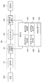
- FIG. 5 is a configuration diagram illustrating an inverter control apparatus according to an embodiment of the present invention.
- the inverter control device 1 is for controlling the inverter 100 in the inverter system as shown in FIG. 2, the output frequency control unit 10, the switching frequency control unit 20 ), an output voltage control unit 30, an output voltage compensation unit 40, and a pulse width modulation (PWM) output unit 50.
- PWM pulse width modulation
- the output frequency control unit 10 may determine an output frequency using the output current of the inverter 100.
- the method of determining the output frequency using the output current is as widely known in the art to which the present invention pertains, and a detailed description thereof will be omitted.
- the output voltage controller 30 may determine the output voltage from the voltage/frequency relationship.
- 6 is an exemplary diagram for explaining a voltage-frequency relationship.
- the output voltage controller 30 may determine the output voltage as 6B from the voltage-frequency relationship line 4A.
- the output voltage compensation unit 40 determines the voltage compensation suppression reference current and the voltage compensation recovery reference current based on the current output frequency, and when the current output current exceeds the suppression reference current, the suppression ratio is increased to reduce the compensation amount. If the current output current is less than the recovery reference current, the amount of compensation can be gradually increased by decreasing the suppression ratio. This will be described with reference to the drawings.
- FIG. 7 is a flowchart illustrating a process of determining an output voltage by an inverter controller according to an embodiment of the present invention.
- the output voltage compensation unit 40 when the output voltage control unit 30 determines the output voltage 6B corresponding to the output frequency 6A, the output voltage compensation unit 40 is voltage-
- the compensation voltage 6C may be determined from the frequency compensation relationship line 4B (S11).
- the output voltage compensation unit 40 may determine a suppression reference current and a recovery reference current for voltage compensation (S12).
- the suppression reference current and the recovery reference current are determined according to the output frequency, and may be determined based on the rated current of the inverter 100.
- Table 1 below is an example of suppression reference current and recovery reference current for voltage compensation.
- the suppression reference current may be determined as 150% of the inverter rated current
- the recovery reference current may be determined as 120% of the inverter rated current.
- suppression/recovery reference current may be determined by temperature simulation data of the junction of the switching device obtained offline and stored in advance in the storage unit (not shown) of the inverter control unit 1, or the output voltage compensation unit (40) may be determined by calculating the amount of heat generated by the switching/conduction loss of the switching device.
- the output voltage compensation unit 40 increases the suppression ratio when the output current of the inverter exceeds the suppression reference current (S15), and determines the final output voltage according to the suppression ratio (S17), and outputs the PWM. It can be provided to the part 50.
- the suppression ratio may be reduced (S16), and a final output voltage may be determined according to the suppression ratio (S17) and provided to the PWM output unit 50.
- the compensation voltage determined in S11 may be determined as the final output voltage and provided to the PWM output unit 50.
- the final output voltage determined by the output voltage compensation unit 40 may be determined by the following equation.
- V boostSupp V boost ⁇ ⁇ supp
- V out V freq -V boostSupp
- V freq is an output voltage determined by the current output frequency, and corresponds to 6B in the example of FIG. 6.
- V boostSupp is the voltage compensation amount reflecting the suppression according to the output current
- V out is the output voltage.
- V boost is a compensation amount before suppressing voltage compensation, which corresponds to 6C determined by the voltage-frequency compensation relationship line 4B.
- ⁇ supp is the suppression ratio determined according to the current output current.
- the output voltage controller 30 outputs 6A as the output voltage V freq by the voltage-frequency relationship line 4A, and the output voltage compensator 40 compensates for 6C.
- V boostSupp is determined by multiplying the voltage V boost by the suppression ratio ⁇ supp . From this, the output voltage V out can be determined as 6D for output.
- the suppression ratio ⁇ supp may be determined and stored in advance in the design stage of the inverter, and this may be determined based on various parameters such as capacity and rated current of the inverter.
- the suppression ratio determined as described above may be stored in a storage unit (not shown) of the inverter.
- the calculation of the compensation voltage of the output voltage compensation unit 40 may be performed periodically. That is, the output current of the inverter 100 is measured for each period, and the compensation voltage may be calculated based on this.
- the switching frequency control unit 20 may determine a maximum switching frequency at which the switching element of the inverter unit 130 is not burned according to the output frequency and the magnitude of the output current.
- the switching frequency may be determined offline using simulation data of the switching device, or may be determined in real time using DC voltage, output current, output frequency, and thermal resistance of the switching device.
- the junction temperature of the switching device can be checked, which can be checked through a known formula. Therefore, the switching frequency when the junction temperature is the maximum without exceeding the rated temperature can be determined as the'maximum switching frequency'.
- the switching frequency control unit 20 provides the switching frequency set by the user to the PWM output unit 50 when the switching frequency set by the user is less than the maximum switching frequency determined above, and when the switching frequency is greater than the maximum switching frequency, the maximum switching frequency is PWM It can be provided to the output unit 50.
- FIG. 8 is a flowchart illustrating a process of determining a switching frequency by an inverter controller according to an embodiment of the present invention.
- the switching frequency controller 20 may determine the maximum switching frequency determined according to the junction temperature of the switching device from the DC voltage, the output frequency and the output current (S21). ).
- the switching frequency control unit 20 may provide the switching frequency as the set switching frequency to the PWM output unit 50 when the set switching frequency for which the user desires the inverter operation is not greater than the maximum switching frequency (S22). (S23).
- the set switching frequency may be input through an interface such as a human-machine interface (HMI) provided to the inverter 100.
- HMI human-machine interface
- the switching frequency control unit 20 may check whether the current switching frequency is less than the maximum switching frequency (S24).
- the switching frequency when the current switching frequency is less than the maximum switching frequency, the switching frequency may be increased (S25) to provide the maximum switching frequency to the PWM output unit 50, and when the current switching frequency is greater than the maximum switching frequency, By reducing the switching frequency (S26), the maximum switching frequency may be provided to the PWM output unit 50.
- the switching frequency control unit 20 of an embodiment of the present invention provides the set switching frequency to the PWM output unit 50 as a final output when the set switching frequency is less than the maximum switching frequency, and the set switching frequency is the maximum switching frequency.
- the maximum switching frequency may be provided to the PWM output unit 50 as a final output.
- the maximum switching frequency may increase in proportion to the output frequency, and when the output frequency decreases, the maximum switching frequency may be lowered. Accordingly, when the inverter accelerates from a stop state, the switching frequency may increase to a set switching frequency set by the user, and when decelerating in a constant speed state, it may decrease from a preset switching frequency to the maximum switching frequency.
- the PMW output unit 50 uses the current angle corresponding to the frequency determined by the output frequency control unit 10 and the output voltage output from the output voltage compensation unit 40 to determine the switching state of the switching device of the inverter unit 130 and The output ratio may be determined and output to the inverter unit 130.
- the output voltage compensation unit provides a compensation amount for the output voltage according to the output frequency, thereby limiting the output current within a certain range. In this way, when overcurrent is applied in a situation where the output frequency is low, it is possible to prevent burnout of the inverter due to instantaneous heat generation of the switching device, and because the rating of the switching device can be optimized relative to the inverter rated current, the product size of the inverter can be optimized. have.
- the present invention relates to an inverter control device, and relates to an inverter control device that prevents thermal damage to an inverter switching device, and thus has industrial applicability.
Landscapes
- Engineering & Computer Science (AREA)
- Power Engineering (AREA)
- Inverter Devices (AREA)
Abstract
Disclosed is an inverter control device. The device of the present invention: determines an output frequency by using an output current of an inverter; determines an output voltage from a voltage-frequency relationship of the inverter; determines a first compensation voltage from a voltage-frequency compensation relationship line; and determines a second compensation voltage suppressing the compensation voltage according to the output current; and determines a final output voltage reflecting the second compensation voltage to the output voltage.
Description
본 발명은 인버터 제어장치에 대한 것이다.The present invention relates to an inverter control device.
일반적으로 인버터는 전기적으로 직류(DC)를 교류(AC)로 변환하는 역변환 장치로써, 산업계에서 사용되는 인버터는 상용전원으로부터 공급된 전력을 입력받아 자체적으로 전압과 주파수를 가변하여 전동기에 공급함으로써 전동기 속도를 고효율로 이용하게 제어하는 일련의 장치로 정의된다. 이러한 인버터는, 가변전압 가변주파수(variable voltage variable frequency, VVVF) 방식에 의해 제어되며, 펄스폭변조(pulse width modulation, PWM) 출력 따라 전동기에 입력되는 전압과 주파수를 가변할 수 있다.In general, an inverter is an inverse conversion device that converts direct current (DC) into alternating current (AC) electrically. Inverters used in the industry receive power supplied from a commercial power source and change their voltage and frequency to supply the motor to the motor. It is defined as a series of devices that control the speed to use with high efficiency. This inverter is controlled by a variable voltage variable frequency (VVVF) method, and can vary a voltage and a frequency input to the motor according to a pulse width modulation (PWM) output.
도 1은 일반적인 인버터의 구성도이다. 1 is a configuration diagram of a general inverter.
일반적으로, 인버터(100)는 계통으로부터 3상의 교류전원을 인가받아, 정류부(110)가 이를 정류하고, 평활부(120)는 정류부(110)가 정류한 직류전압을 평활하여 저장한다. 인버터부(130)는 평활부(120)인 직류링크 커패시터에 저장된 직류전압  를 PWM 제어신호에 따라 소정 전압 및 주파수를 가지는 교류전압을 출력하여, 이를 전동기에 제공한다. 인버터부(130)는 3상의 레그로 구성되며, 각 레그에는 2개의 스위칭 소자가 직렬로 연결되어 구성된다. In general, the
 inverter 100 receives 3-phase AC power from the grid, the rectifier 110 rectifies it, and the smoothing unit 120 smoothes and stores the DC voltage rectified by the rectifier 110. The inverter unit 130 is a DC voltage stored in the DC link capacitor which is the smoothing unit 120 Outputs an AC voltage having a predetermined voltage and frequency according to the PWM control signal, and provides it to the motor. The inverter unit 130 is composed of three-phase legs, and two switching elements are connected in series to each leg.
이러한 인버터부(130)의 스위칭소자는 전력소자로서, 예를 들어 절연 게이트 양극성 트랜지스터(insulated gate bipolar transistor, IGBT)가 보통 이용된다. 이러한 전력소자는 스위칭 주파수에 비례하여 스위칭 손실이 커진다. 또한 스위칭 주파수가 동일하고 최대값이 같은 크기의 교류전류가 흐를 때 IGBT의 접합부 온도의 최대값은 출력전류의 주파수가 낮을 때 더욱 높아진다.The switching device of the inverter unit 130 is a power device, for example, an insulated gate bipolar transistor (IGBT) is usually used. Such a power device has a large switching loss in proportion to the switching frequency. In addition, when the switching frequency is the same and the AC current of the same maximum value flows, the maximum value of the junction temperature of the IGBT becomes higher when the frequency of the output current is low.
따라서, 인버터의 최대 정격출력보다 수배 이상 큰 정격전류를 가지는 IGBT를 사용하게 되면 동일 출력전류 대비 접합부의 온도상승이 적기 때문에 열에 의한 소손이 발생하지 않는다. 그러나 제품의 크기 및 원가를 줄이기 위하여 인버터의 정격전류에 최적화된 IGBT를 선택하게 되고, 이러한 경우 출력주파수, 출력전류 및 스위칭 주파수 조건에 따라 IGBT의 열적 소손이 발생할 수 있으며, 이는 인버터(100)의 전체 시스템 효율저하의 큰 원인이 되는 문제점이 있다.Therefore, when an IGBT having a rated current that is several times larger than the maximum rated output of the inverter is used, the temperature rise of the junction is small compared to the same output current, so that heat damage does not occur. However, in order to reduce the size and cost of the product, an IGBT optimized for the rated current of the inverter is selected. In this case, thermal burnout of the IGBT may occur depending on the output frequency, output current, and switching frequency conditions. There is a problem that is a major cause of lowering the overall system efficiency.
본 발명이 해결하고자 하는 기술적 과제는, 인버터 스위칭소자의 열적손상을 방지하는, 인버터 제어장치를 제공하는 것이다.The technical problem to be solved by the present invention is to provide an inverter control device that prevents thermal damage to the inverter switching device.
상기와 같은 기술적 과제를 해결하기 위해, 본 발명의 일실시예의 인버터 제어장치는, 인버터의 출력전류를 이용하여 출력주파수를 결정하는 제1결정부; 상기 인버터의 전압-주파수 관계로부터 출력전압을 결정하는 제2결정부; 및 전압-주파수 보상관계선으로부터 제1보상전압을 결정하고, 출력전류에 따라 상기 보상전압을 억제한 제2보상전압을 결정하여, 상기 출력전압에 상기 제2보상전압을 반영한 최종 출력전압을 결정하는 제3결정부를 포함할 수 있다.In order to solve the above technical problem, an inverter control apparatus according to an embodiment of the present invention includes: a first determination unit configured to determine an output frequency using an output current of the inverter; A second determination unit determining an output voltage from the voltage-frequency relationship of the inverter; And determining a first compensation voltage from a voltage-frequency compensation relationship line, determining a second compensation voltage suppressing the compensation voltage according to an output current, and determining a final output voltage reflecting the second compensation voltage in the output voltage. It may include a third decision unit.
본 발명의 일실시예에서, 상기 제3결정부는, 상기 출력주파수를 이용하여 전압보상을 위한 제1기준전류와 상기 제1기준전류보다 작은 제2기준전류를 결정하고, 상기 제1기준전류 및 제2기준전류에 대한 현재 출력전류의 크기에 따라 상기 최종 출력전압을 결정할 수 있다.In an embodiment of the present invention, the third determining unit determines a first reference current for voltage compensation and a second reference current smaller than the first reference current by using the output frequency, and the first reference current and The final output voltage may be determined according to the magnitude of the current output current with respect to the second reference current.
본 발명의 일실시예에서, 상기 제3결정부는, 상기 출력주파수에 따라 상기 인버터의 정격전류를 기준으로 상기 제1 및 제2기준전류를 결정할 수 있다.In one embodiment of the present invention, the third determining unit may determine the first and second reference currents based on the rated current of the inverter according to the output frequency.
본 발명의 일실시예에서, 상기 제3결정부는, 출력전류가 상기 제1기준전류를 초과하는 경우 억제비율을 증가하여, 상기 억제비율에 따라 상기 최종 출력전압을 결정할 수 있다.In one embodiment of the present invention, the third determining unit may increase a suppression ratio when the output current exceeds the first reference current, and determine the final output voltage according to the suppression ratio.
본 발명의 일실시예에서, 상기 제3결정부는, 출력전류가 상기 제2기준전류 미만인 경우 억제비율을 감소하여, 상기 억제비율에 따라 상기 최종 출력전압을 결정할 수 있다.In one embodiment of the present invention, the third determining unit may determine the final output voltage according to the suppression ratio by decreasing a suppression ratio when the output current is less than the second reference current.
본 발명의 일실시예에서, 상기 제3결정부는, 아래 수학식에 의해 상기 최종 출력전압을 결정할 수 있다.In one embodiment of the present invention, the third determining unit may determine the final output voltage by the following equation.
Vout = Vfreq - VboostSupp
V out = V freq -V boostSupp
이때 Vout은 상기 최종 출력전압이고, Vfreq은 상기 출력전압이고, VboostSupp=Vboost×αsupp이고, Vboost은 상기 제1보상전압이고, VboostSupp는 상기 제2보상전압이고, αsupp는 상기 억제비율이다.At this time, V out is the final output voltage, V freq is the output voltage, V boostSupp = V boost × α supp , V boost is the first compensation voltage, V boostSupp is the second compensation voltage, α supp Is the inhibition ratio.
또한, 상기와 같은 기술적 과제를 해결하기 위해, 본 발명의 일실시예의 인버터 제어장치는, 인버터의 출력전류를 이용하여 출력주파수를 결정하는 제1결정부; 및 상기 출력주파수 및 상기 인버터의 직류전압 및 출력전류의 크기에 따라, 상기 인버터의 스위칭소자에 대한 최대 스위칭 주파수를 결정하고, 상기 최대 스위칭 주파수에 대한 미리 설정된 설정 스위칭 주파수의 크기에 따라 최종 스위칭 주파수를 결정하는 제2결정부를 포함할 수 있다. In addition, in order to solve the technical problem as described above, the inverter control apparatus according to an embodiment of the present invention includes: a first determination unit for determining an output frequency using the output current of the inverter; And determining the maximum switching frequency for the switching device of the inverter according to the output frequency and the magnitude of the DC voltage and output current of the inverter, and a final switching frequency according to the magnitude of a preset switching frequency for the maximum switching frequency. It may include a second determination unit to determine the.
본 발명의 일실시예에서, 상기 제2결정부는, 상기 직류전압, 출력주파수 및 출력전류로부터 상기 스위칭소자의 접합부 온도를 결정하고, 상기 인버터의 정격온도를 초과하지 않으면서 상기 스위칭소자의 접합부 온도가 최대인 경우의 스위칭 주파수를 상기 최대 스위칭 주파수로 결정할 수 있다.In one embodiment of the present invention, the second determining unit determines a junction temperature of the switching device from the DC voltage, output frequency, and output current, and the junction temperature of the switching device does not exceed the rated temperature of the inverter. The switching frequency in the case where is the maximum may be determined as the maximum switching frequency.
본 발명의 일실시예에서, 상기 제2결정부는, 상기 설정 스위칭 주파수가 상기 최대 스위칭 주파수보다 작거나 같은 경우에는, 상기 설정 스위칭 주파수를 상기 최종 스위칭 주파수로써 출력할 수 있다.In an embodiment of the present invention, the second determining unit may output the set switching frequency as the final switching frequency when the set switching frequency is less than or equal to the maximum switching frequency.
본 발명의 일실시예에서, 상기 제2결정부는, 상기 설정 스위칭 주파수가 상기 최대 스위칭 주파수보다 큰 경우에는, 상기 최대 스위칭 주파수를 상기 최종 스위칭 주파수로써 출력할 수 있다.In an embodiment of the present invention, the second determining unit may output the maximum switching frequency as the final switching frequency when the set switching frequency is greater than the maximum switching frequency.
본 발명의 일실시예에서, 상기 제2결정부는, 상기 설정 스위칭 주파수가 상기 최대 스위칭 주파수보다 크고, 현재 스위칭 주파수가 상기 최대 스위칭 주파수보다 작은 경우, 스위칭 주파수를 증가하여 상기 최대 스위칭 주파수를 상기 최종 스위칭 주파수로써 출력할 수 있다.In an embodiment of the present invention, the second determining unit, when the set switching frequency is greater than the maximum switching frequency and the current switching frequency is less than the maximum switching frequency, increases the switching frequency to reduce the maximum switching frequency to the final It can be output as a switching frequency.
본 발명의 일실시예에서, 상기 제2결정부는, 상기 설정 스위칭 주파수가 상기 최대 스위칭 주파수보다 크고, 현재 스위칭 주파수가 상기 최대 스위칭 주파수보다 큰 경우, 스위칭 주파수를 감소하여 상기 최대 스위칭 주파수를 상기 최종 스위칭 주파수로써 출력할 수 있다. In an embodiment of the present invention, the second determining unit, when the set switching frequency is greater than the maximum switching frequency, and the current switching frequency is greater than the maximum switching frequency, decreases the switching frequency to reduce the maximum switching frequency to the final It can be output as a switching frequency.
또한, 상기와 같은 기술적 과제를 해결하기 위해, 본 발명의 일실시예의 인버터 제어장치는, 인버터의 출력전류를 이용하여 출력주파수를 결정하는 제1결정부; 상기 인버터의 전압-주파수 관계로부터 출력전압을 결정하는 제2결정부; 전압-주파수 보상관계선으로부터 제1보상전압을 결정하고, 출력전류에 따라 상기 보상전압을 억제한 제2보상전압을 결정하여, 상기 출력전압에 상기 제2보상전압을 반영한 최종 출력전압을 결정하는 제3결정부; 및 상기 출력주파수 및 상기 인버터의 직류전압 및 출력전류의 크기에 따라, 상기 인버터의 스위칭소자에 대한 최대 스위칭 주파수를 결정하고, 상기 최대 스위칭 주파수에 대한 미리 설정된 설정 스위칭 주파수의 크기에 따라 최종 스위칭 주파수를 결정하는 제4결정부를 포함할 수 있다.In addition, in order to solve the technical problem as described above, the inverter control apparatus according to an embodiment of the present invention includes: a first determination unit for determining an output frequency using the output current of the inverter; A second determination unit determining an output voltage from the voltage-frequency relationship of the inverter; Determining a first compensation voltage from a voltage-frequency compensation relationship line, determining a second compensation voltage suppressing the compensation voltage according to an output current, and determining a final output voltage reflecting the second compensation voltage in the output voltage A third decision unit; And determining the maximum switching frequency for the switching device of the inverter according to the output frequency and the magnitude of the DC voltage and output current of the inverter, and a final switching frequency according to the magnitude of a preset switching frequency for the maximum switching frequency. It may include a fourth determination unit to determine the.
상기와 같은 본 발명은, 인버터 출력주파수에 따라 출력전압에 대한 보상량을 제공함으로써, 출력전류를 일정 범위내로 제한함으로써, 출력주파수가 낮은 상황에서 과전류가 인가되는 경우 스위칭소자의 순간 발열에 의한 인버터의 소손을 방지할 수 있고, 인버터 정격전류 대비 스위칭소자의 정격을 최적화할 수 있으므로, 인버터 제품크기를 최적화하는 효과가 있다. The present invention as described above, by providing a compensation amount for the output voltage according to the inverter output frequency, by limiting the output current to within a certain range, the inverter due to instantaneous heat generation of the switching element when an overcurrent is applied in a situation where the output frequency is low. It is possible to prevent burnout of the inverter and optimize the rating of the switching device relative to the rated current of the inverter, thus optimizing the inverter product size.
또한, 본 발명은 인버터의 직류전압, 출력주파수 및 출력전류에 따라 스위칭 주파수를 제한함으로써, 스위칭소자의 스위칭 손실을 줄여 스위칭소자의 순간 발열에 의한 인버터의 소손을 방지할 수 있고, 스위칭소자가 소손되지 않는 최적의 스위칭 주파수에서 운전가능하므로, 전동기 소음을 감소하게 하는 효과가 있다.In addition, according to the present invention, by limiting the switching frequency according to the DC voltage, output frequency and output current of the inverter, it is possible to reduce the switching loss of the switching device to prevent burnout of the inverter due to instantaneous heat generation of the switching device. Since it is possible to operate at an optimal switching frequency that is not possible, there is an effect of reducing motor noise.
도 1은 일반적인 인버터의 구성도이다.1 is a configuration diagram of a general inverter.
도 2는 종래의 인버터 시스템의 구성도이다.2 is a block diagram of a conventional inverter system.
도 3은 종래의 출력전압 보상을 설명하기 위한 예시도이다.3 is an exemplary diagram for explaining a conventional output voltage compensation.
도 4는 종래의 출력전압 보상을 설명하기 위한 예시도이다.4 is an exemplary diagram for explaining conventional output voltage compensation.
도 5는 본 발명의 일실시예의 인버터 제어장치를 설명하기 위한 구성도이다.5 is a configuration diagram illustrating an inverter control apparatus according to an embodiment of the present invention.
도 6은 전압-주파수 관계를 설명하기 위한 일예시도이다.6 is an exemplary diagram for explaining a voltage-frequency relationship.
도 7은 본 발명의 일실시예의 인버터 제어부가 출력전압을 결정하는 과정을 설명하기 위한 흐름도이다.7 is a flowchart illustrating a process of determining an output voltage by an inverter controller according to an embodiment of the present invention.
도 8은 본 발명의 일실시예의 인버터 제어부가 스위칭 주파수를 결정하는 과정을 설명하기 위한 흐름도이다.8 is a flowchart illustrating a process of determining a switching frequency by an inverter controller according to an embodiment of the present invention.
[부호의 설명][Explanation of code]
10: 출력주파수 제어부 20: 스위칭 주파수 제어부10: output frequency control unit 20: switching frequency control unit
30: 출력전압 제어부 40: 출력전압 보상부30: output voltage control unit 40: output voltage compensation unit
50: PWM 출력부50: PWM output
본 발명의 구성 및 효과를 충분히 이해하기 위하여, 첨부한 도면을 참조하여 본 발명의 바람직한 실시예들을 설명한다. 그러나 본 발명은 이하에서 개시되는 실시예에 한정되는 것이 아니라, 여러가지 형태로 구현될 수 있고 다양한 변경을 가할 수 있다. 단지, 본 실시예에 대한 설명은 본 발명의 개시가 완전하도록 하며, 본 발명이 속하는 기술분야의 통상의 지식을 가진 자에게 발명의 범주를 완전하게 알려주기 위하여 제공되는 것이다. 첨부된 도면에서 구성요소는 설명의 편의를 위하여 그 크기를 실제보다 확대하여 도시한 것이며, 각 구성요소의 비율은 과장되거나 축소될 수 있다.In order to fully understand the configuration and effects of the present invention, preferred embodiments of the present invention will be described with reference to the accompanying drawings. However, the present invention is not limited to the embodiments disclosed below, but may be implemented in various forms and various modifications may be added. However, the description of the present embodiment is provided to complete the disclosure of the present invention, and to fully inform a person of ordinary skill in the art to which the present invention belongs. In the accompanying drawings, for convenience of description, the size of the components is enlarged compared to the actual size, and the ratio of each component may be exaggerated or reduced.
'제1', '제2' 등의 용어는 다양한 구성요소를 설명하는데 사용될 수 있지만, 상기 구성요소는 위 용어에 의해 한정되어서는 안 된다. 위 용어는 하나의 구성요소를 다른 구성요소로부터 구별하는 목적으로만 사용될 수 있다. 예를 들어, 본 발명의 권리범위를 벗어나지 않으면서 '제1구성요소'는 '제2구성요소'로 명명될 수 있고, 유사하게 '제2구성요소'도 '제1구성요소'로 명명될 수 있다. 또한, 단수의 표현은 문맥상 명백하게 다르게 표현하지 않는 한, 복수의 표현을 포함한다. 본 발명의 실시예에서 사용되는 용어는 다르게 정의되지 않는 한, 해당 기술분야에서 통상의 지식을 가진 자에게 통상적으로 알려진 의미로 해석될 수 있다.Terms such as'first' and'second' may be used to describe various elements, but the elements should not be limited by the above terms. The above terms may be used only for the purpose of distinguishing one component from other components. For example, without departing from the scope of the rights of the present invention, the'first element' may be referred to as the'second element', and similarly, the'second element' may also be named as the'first element'. I can. In addition, expressions in the singular include plural expressions unless clearly expressed otherwise in context. Unless otherwise defined, terms used in the embodiments of the present invention may be interpreted as meanings commonly known to those of ordinary skill in the art.
이하에서는, 도 2 내지 도 4를 참조하여, 종래의 인버터 시스템에서의 제어방법에 대해 설명하고, 도 5 내지 도 8을 참조하여 본 발명의 인버터 제어장치 및 그 방법에 대해 설명하기로 한다. Hereinafter, a control method in a conventional inverter system will be described with reference to FIGS. 2 to 4, and an inverter control apparatus and method thereof of the present invention will be described with reference to FIGS. 5 to 8.
도 2는 종래의 인버터 시스템의 구성도이다.2 is a block diagram of a conventional inverter system.
도면에 도시된 바와 같이, 본 발명의 일실시예의 인버터 시스템에서, 인버터(100)는 전원(200)으로부터 3상 전원을 입력받아 전동기(300)로 소정의 주파수 및 크기의 전압을 출력하는 것으로서, 정류부(110), 직류전압 검출부(120), 인버터부(130), 및 출력전류 검출부(140)로 구성된다. As shown in the drawing, in the inverter system of an embodiment of the present invention, the inverter 100 receives three-phase power from the power source 200 and outputs a voltage of a predetermined frequency and size to the electric motor 300, It is composed of a rectifying unit 110, a DC voltage detection unit 120, an inverter unit 130, and an output current detection unit 140.
또한, 도 1의 인버터 시스템은, 인버터(100)를 제어하는 제어부(400)를 포함하며, 제어부(400)는 출력주파수 제어부(410), 스위칭 주파수 제어부(420), 출력전압 제어부(430), 출력전압 보상부(440) 및 펄스폭변조(PWM) 출력부(450)로 구성된다. In addition, the inverter system of FIG. 1 includes a control unit 400 that controls the inverter 100, and the control unit 400 includes an output frequency control unit 410, a switching frequency control unit 420, an output voltage control unit 430, It is composed of an output voltage compensation unit 440 and a pulse width modulation (PWM) output unit 450.
인버터(100)의 정류부(110)는 3상 전원을 정류하여 직류로 변환하고, 인버터부(130)는 직류전압을 제어부(400)의 제어에 의해 소정 주파수 및 크기의 전압으로 변환하여 출력한다. The rectifier 110 of the inverter 100 rectifies and converts the three-phase power into DC, and the inverter 130 converts the DC voltage into a voltage of a predetermined frequency and size under the control of the controller 400 and outputs the converted voltage.
출력주파수 제어부(410)는 출력전류가 소정 주파수로 출력될 수 있도록 제어하고, 스위칭 주파수 제어부(420)는 인버터부(130)의 스위칭 주파수를 제어하여 PWM 제어가 동작할 수 있도록 한다.The output frequency controller 410 controls the output current to be output at a predetermined frequency, and the switching frequency controller 420 controls the switching frequency of the inverter unit 130 so that the PWM control can be operated.
출력전압 제어부(430)는 출력주파수 제어부(410)에 의해 결정된 출력주파수에 해당하는 출력전압을 결정하고, 출력전압 보상부(440)는 저속에서 전동기(300)의 기동토크를 확보하기 위해 출력전압 제어부(430)에 의해 결정된 출력전압에 일정량의 보상한다. The output voltage control unit 430 determines the output voltage corresponding to the output frequency determined by the output frequency control unit 410, and the output voltage compensation unit 440 is used to secure the starting torque of the motor 300 at a low speed. The output voltage determined by the control unit 430 is compensated by a certain amount.
또한, PWM 출력부(450)는 출력주파수 제어부(410)에 의해 결정된 현재 각도, 출력전압 제어부(430) 및 출력전압 보상부(440)에 의해 결정된 출력전압으로 3상의 온오프 상태 및 출력비(duty)를 결정하여 출력한다.In addition, the PWM output unit 450 is the current angle determined by the output frequency control unit 410, the output voltage determined by the output voltage control unit 430 and the output voltage compensation unit 440, and the three-phase on-off state and output ratio (duty). ) Is determined and printed.
도 3은 종래의 인버터 제어방법의 흐름도로서, 인버터 제어부(400)의 동작의 흐름을 나타낸다.3 is a flow chart of a conventional inverter control method, showing the flow of the operation of the inverter control unit 400.
즉, 출력주파수 제어부(410)가 출력주파수를 결정하고(S310), 이에 대응하여 출력전압을 결정하고(S320), 출력전압을 보상한다(S330).That is, the output frequency controller 410 determines an output frequency (S310), determines an output voltage corresponding thereto (S320), and compensates the output voltage (S330).
이후, 출력주파수 제어부(410)에 의해 결정된 출력주파수에 대응하는 현재 각도를 결정하고(S340), 이를 이용하여 3상 PWM 변환을 수행하고(S350), PWM 신호를 출력한다(S360). Thereafter, the current angle corresponding to the output frequency determined by the output frequency controller 410 is determined (S340), and a 3-phase PWM conversion is performed using this (S350), and a PWM signal is output (S360).
이후, 인버터 출력주파수가 목표주파수에 도달할 때까지 위의 제어를 수행한다(S370).Thereafter, the above control is performed until the inverter output frequency reaches the target frequency (S370).
도 4는 종래의 출력전압 보상을 설명하기 위한 예시도이다.4 is an exemplary diagram for explaining conventional output voltage compensation.
종래의 인버터 시스템에서는, 기저주파수 미만의 주파수에서 일정량의 전압을 보상하여 출력한다. 즉, 출력전압 제어부(430)에 의해 출력주파수에 대응하는 출력전압이 결정되면(4A), 출력전압 보상부(440)가 이를 보상하여 4B와 같은 보상전압을 출력한다. 예를 들어, 4E에 대응하는 출력전압 4C를 출력전압 제어부(430)가 결정하는 경우, 출력전압 보상부(440)는 이를 보상하여 4D의 출력전압을 출력하는 것이다.In a conventional inverter system, a certain amount of voltage is compensated and output at a frequency less than the base frequency. That is, when the output voltage corresponding to the output frequency is determined by the output voltage control unit 430 (4A), the output voltage compensation unit 440 compensates for it and outputs a compensation voltage equal to 4B. For example, when the output voltage controller 430 determines the output voltage 4C corresponding to 4E, the output voltage compensation unit 440 compensates for the output voltage 4C to output a 4D output voltage.
기저주파수의 출력전압은 출력전압 보상을 적용하지 않은 경우와 동일해짐을 알 수 있다.It can be seen that the output voltage of the base frequency is the same as the case where the output voltage compensation is not applied.
그런데, 이러한 경우 출력주파수가 낮을수록 원래의 출력전압 제어부(430)에 의해 결정되는 출력전압이 보상되어 매우 큰 전압이 인가되므로 과전류가 발생하며, 이러한 경우, 인버터부(130)의 IGBT 접합부의 순간온도의 최대치가 크게 상승하여, IGBT의 열적 소손을 야기한다. However, in this case, as the output frequency is lower, the output voltage determined by the original output voltage control unit 430 is compensated and a very large voltage is applied, so an overcurrent occurs. In this case, the moment of the IGBT junction of the inverter unit 130 The maximum value of the temperature rises significantly, causing thermal burnout of the IGBT.
또한, 출력전류의 크기 및 출력주파수와 관계없이 기설정된 스위칭 주파수로 임의의 전압을 출력하므로, 스위칭 주파수가 높은 경우 인버터부(130)의 IGBT 접합부의 순간온도 최대치가 급격히 상승하여 IGBT의 열적소손을 야기한다.In addition, since an arbitrary voltage is output at a preset switching frequency regardless of the size of the output current and the output frequency, when the switching frequency is high, the maximum instantaneous temperature of the IGBT junction of the inverter unit 130 rises rapidly to reduce thermal burnout of the IGBT. Cause.
일반적으로 인버터부(130)의 암-쇼트(arm-short)를 방지하기 위해, 인버터(100)의 제어기는 어퍼암(upper-arm)과 로워암(lower-arm)에 인가하는 게이트신호를 항상 상보적으로 출력한다. 그러나, IGBT에 소손이 발생되면, 제어기는 어퍼암과 로워암의 게이트신호를 상보적으로 출력하지만, 소손에 의해 실제 게이트 전압이 이와 다르게 모두 턴온 레벨 이상으로 인가될 수 있다. 이경우 암-쇼트가 발생하고, 순간적으로 과전류가 흐르게 되며, 이에 의해 인버터는 암-쇼트 고장이 발생하게 된다. In general, in order to prevent an arm-short of the inverter unit 130, the controller of the inverter 100 always applies a gate signal to the upper-arm and the lower-arm. Outputs complementarily. However, when burnout occurs in the IGBT, the controller outputs the gate signals of the upper arm and the lower arm complementarily, but the actual gate voltage may be differently applied due to the burnout and above the turn-on level. In this case, an arm-short occurs, and an instantaneous overcurrent flows, thereby causing an arm-short fault in the inverter.
본 발명은, 위와 같은 문제점을 해결하기 위한 것으로서, 낮은 출력주파수에 의한 높은 출력전류 발생시 또는 높은 스위칭 주파수에서도 인버터부(130)의 스위칭소자의 접합부에서 순간 최대온도를 초과하는 경우에도 스위칭소자의 열적손상을 방지하고 안정적으로 인버터를 제어하기 위한 것이다.The present invention is to solve the above problems, even when a high output current is generated due to a low output frequency or a high switching frequency, even when the instantaneous maximum temperature is exceeded at the junction of the switching device of the inverter unit 130 It is to prevent damage and control the inverter stably.
도 5는 본 발명의 일실시예의 인버터 제어장치를 설명하기 위한 구성도이다.5 is a configuration diagram illustrating an inverter control apparatus according to an embodiment of the present invention.
도면에 도시된 바와 같이, 본 발명의 일실시예의 인버터 제어장치(1)는, 도 2와 같은 인버터 시스템에서 인버터(100)를 제어하기 위한 것으로서, 출력주파수 제어부(10), 스위칭 주파수 제어부(20), 출력전압 제어부(30), 출력전압 보상부(40) 및 펄스폭변조(PWM) 출력부(50)를 포함할 수 있다.As shown in the drawing, the inverter control device 1 according to an embodiment of the present invention is for controlling the inverter 100 in the inverter system as shown in FIG. 2, the output frequency control unit 10, the switching frequency control unit 20 ), an output voltage control unit 30, an output voltage compensation unit 40, and a pulse width modulation (PWM) output unit 50.
본 발명의 일실시예의 출력주파수 제어부(10)는, 인버터(100)의 출력전류를 이용하여 출력주파수를 결정할 수 있다. 출력전류를 이용하여 출력주파수를 결정하는 방식에 대해서는, 본 발명이 속하는 기술분야에서 널리 알려진 바와 같으므로, 그 상세한 설명은 생략하기로 한다.The output frequency control unit 10 according to an embodiment of the present invention may determine an output frequency using the output current of the inverter 100. The method of determining the output frequency using the output current is as widely known in the art to which the present invention pertains, and a detailed description thereof will be omitted.
출력전압 제어부(30)는 전압/주파수 관계로부터 출력전압을 결정할 수 있다. 도 6은 전압-주파수 관계를 설명하기 위한 일예시도이다.The output voltage controller 30 may determine the output voltage from the voltage/frequency relationship. 6 is an exemplary diagram for explaining a voltage-frequency relationship.
도면에 도시된 바와 같이, 출력주파수 제어부(10)에 의해 출력주파수가 6A로 결정되면, 출력전압 제어부(30)는 전압-주파수 관계선(4A)으로부터 출력전압을 6B로 결정할 수 있다.As shown in the drawing, when the output frequency is determined to be 6A by the output frequency controller 10, the output voltage controller 30 may determine the output voltage as 6B from the voltage-frequency relationship line 4A.
출력전압 보상부(40)는 현재 출력주파수를 기반으로 전압보상 억제 기준전류와 전압보상 회복 기준전류를 결정하여, 현재 출력전류가 억제 기준전류를 초과하는 경우 억제비율을 점증하여 보상량을 절감하고, 현재 출력전류가 회복 기준전류 미만인 경우 억제비율을 점감하여 보상량을 점증시킬 수 있다. 이를 도면을 참조로 설명하기로 한다.The output voltage compensation unit 40 determines the voltage compensation suppression reference current and the voltage compensation recovery reference current based on the current output frequency, and when the current output current exceeds the suppression reference current, the suppression ratio is increased to reduce the compensation amount. If the current output current is less than the recovery reference current, the amount of compensation can be gradually increased by decreasing the suppression ratio. This will be described with reference to the drawings.
도 7은 본 발명의 일실시예의 인버터 제어부가 출력전압을 결정하는 과정을 설명하기 위한 흐름도이다.7 is a flowchart illustrating a process of determining an output voltage by an inverter controller according to an embodiment of the present invention.
도면에 도시된 바와 같이, 본 발명의 일실시예의 방법은, 출력전압 제어부(30)가 출력주파수(6A)에 대응하는 출력전압(6B)을 결정하면, 출력전압 보상부(40)는 전압-주파수 보상관계선(4B)으로부터 보상전압(6C)을 결정할 수 있다(S11).As shown in the figure, in the method of an embodiment of the present invention, when the output voltage control unit 30 determines the output voltage 6B corresponding to the output frequency 6A, the output voltage compensation unit 40 is voltage- The compensation voltage 6C may be determined from the frequency compensation relationship line 4B (S11).
이후, 출력전압 보상부(40)는 전압보상을 위한 억제 기준전류 및 회복 기준전류를 결정할 수 있다(S12). Thereafter, the output voltage compensation unit 40 may determine a suppression reference current and a recovery reference current for voltage compensation (S12).
이때 억제 기준전류 및 회복 기준전류는 출력주파수에 따라 결정되는 것으로서, 인버터(100)의 정격전류를 기준으로 결정될 수 있다. 다음의 표 1은 전압보상을 위한 억제 기준전류와 회복 기준전류의 일예이다. 예를 들어, 출력주파수가 1Hz인 경우 억제 기준전류는 인버터 정격전류의 150%로 결정될 수 있고, 회복 기준전류는 인버터 정격전류의 120%로 결정될 수 있을 것이다. At this time, the suppression reference current and the recovery reference current are determined according to the output frequency, and may be determined based on the rated current of the inverter 100. Table 1 below is an example of suppression reference current and recovery reference current for voltage compensation. For example, when the output frequency is 1Hz, the suppression reference current may be determined as 150% of the inverter rated current, and the recovery reference current may be determined as 120% of the inverter rated current.
| 출력주파수Output frequency |
~1Hz~ |
1~5Hz1~5Hz | 5~60Hz5~60Hz |
| 억제 기준전류Suppression reference current | 150%150% | 150~180%150~180% | 180%180% |
| 회복 기준전류Recovery reference current | 120%120% | 120~150%120~150% | 150%150% |
이와 같은 억제/회복 기준전류의 예시는 오프라인으로 획득한 스위칭소자의 접합부의 온도 시뮬레이션 데이터에 의해서 결정되어 미리 인버터 제어부(1)의 저장부(도시되지 않음)에 저장될 수도 있고, 출력전압 보상부(40)가 스위칭소자의 스위칭/컨덕션 손실에 의한 발열량을 계산하여 결정할 수도 있다. 도 7에서, 출력전압 보상부(40)는, 인버터의 출력전류가 억제 기준전류를 초과하는 경우에는 억제비율을 증가하고(S15), 억제비율에 따라 최종 출력전압을 결정하여(S17) PWM 출력부(50)에 제공할 수 있다. An example of such a suppression/recovery reference current may be determined by temperature simulation data of the junction of the switching device obtained offline and stored in advance in the storage unit (not shown) of the inverter control unit 1, or the output voltage compensation unit (40) may be determined by calculating the amount of heat generated by the switching/conduction loss of the switching device. In FIG. 7, the output voltage compensation unit 40 increases the suppression ratio when the output current of the inverter exceeds the suppression reference current (S15), and determines the final output voltage according to the suppression ratio (S17), and outputs the PWM. It can be provided to the part 50.
S13에서 출력전류가 억제 기준전류를 초과하지 않는 경우, 출력전류가 회복 기준전류 미만인지 확인할 수 있다(S14). S14에서 출력전류가 회복 기준전류 미만인 경우에는 억제비율을 감소하고(S16), 억제비율에 따라 최종 출력전압을 결정하여(S17) PWM 출력부(50)에 제공할 수 있다.When the output current does not exceed the suppression reference current in S13, it can be checked whether the output current is less than the recovery reference current (S14). When the output current is less than the recovery reference current in S14, the suppression ratio may be reduced (S16), and a final output voltage may be determined according to the suppression ratio (S17) and provided to the PWM output unit 50.
S14에서 출력전류가 회복 기준전류 미만이 아닌 경우, S11에서 결정한 보상전압을 최종 출력전압으로 결정하여 PWM 출력부(50)에 제공할 수 있을 것이다.When the output current in S14 is not less than the recovery reference current, the compensation voltage determined in S11 may be determined as the final output voltage and provided to the PWM output unit 50.
이때, 출력전압 보상부(40)가 결정하는 최종 출력전압은 다음 수학식에 의해 결정될 수 있다.In this case, the final output voltage determined by the output voltage compensation unit 40 may be determined by the following equation.
[수학식 1][Equation 1]
VboostSupp = Vboost × αsupp
V boostSupp = V boost × α supp
[수학식 2][Equation 2]
Vout = Vfreq - VboostSupp
V out = V freq -V boostSupp
이때 Vfreq는 현재의 출력주파수에 의해 결정되는 출력전압으로서, 도 6의 일예에서 6B에 해당한다. VboostSupp는 출력전류에 따라 억제가 반영된 전압보상량이고, Vout은 출력전압이다. 또한, Vboost는 전압보상을 억제하기 이전의 보상량으로서, 전압-주파수 보상관계선(4B)에 의해 결정되는 6C에 해당하는 것이다. 또한, αsupp는 현재 출력전류에 따라 결정되는 억제비율이다. At this time, V freq is an output voltage determined by the current output frequency, and corresponds to 6B in the example of FIG. 6. V boostSupp is the voltage compensation amount reflecting the suppression according to the output current, and V out is the output voltage. In addition, V boost is a compensation amount before suppressing voltage compensation, which corresponds to 6C determined by the voltage-frequency compensation relationship line 4B. Also, α supp is the suppression ratio determined according to the current output current.
도 6에서, 6A에 해당하는 출력주파수에서, 출력전압 제어부(30)는 전압-주파수 관계선(4A)에 의해 6A를 출력전압 Vfreq로 출력하고, 출력전압 보상부(40)는 6C인 보상전압 Vboost에 억제비율 αsupp를 곱하여 VboostSupp를 결정하며, 이로부터 출력전압 Vout을 예를 들어 6D로 결정하여 출력할 수 있다.In FIG. 6, at the output frequency corresponding to 6A, the output voltage controller 30 outputs 6A as the output voltage V freq by the voltage-frequency relationship line 4A, and the output voltage compensator 40 compensates for 6C. V boostSupp is determined by multiplying the voltage V boost by the suppression ratio α supp . From this, the output voltage V out can be determined as 6D for output.
이때 억제비율 αsupp은 인버터의 설계단계에서 미리 결정되어 저장될 수 있으며, 이는 인버터의 용량, 정격전류 등 다양한 파라미터를 기준으로 하여 결정될 수 있을 것이다. 이와 같이 결정된 억제비율은 인버터의 저장부(도시되지 않음)에 저장될 수 있다. At this time, the suppression ratio α supp may be determined and stored in advance in the design stage of the inverter, and this may be determined based on various parameters such as capacity and rated current of the inverter. The suppression ratio determined as described above may be stored in a storage unit (not shown) of the inverter.
본 발명의 일실시예에서, 출력전압 보상부(40)의 보상전압 계산은 주기적으로 수행될 수 있다. 즉, 주기마다 인버터(100)의 출력전류를 측정하여, 이를 기준으로 보상전압을 계산할 수 있을 것이다.In one embodiment of the present invention, the calculation of the compensation voltage of the output voltage compensation unit 40 may be performed periodically. That is, the output current of the inverter 100 is measured for each period, and the compensation voltage may be calculated based on this.
한편, 스위칭 주파수 제어부(20)는, 출력주파수와 출력전류의 크기에 따라, 인버터부(130)의 스위칭소자가 소손되지 않는 최대 스위칭 주파수를 결정할 수 있다. 이러한 스위칭 주파수는 스위칭소자의 시뮬레이션 데이터를 이용하여 오프라인으로 결정할 수도 있고, 또는, 직류전압, 출력전류, 출력주파수, 및 스위칭소자의 열저항 등을 이용하여 실시간으로 결정할 수도 있다. Meanwhile, the switching frequency control unit 20 may determine a maximum switching frequency at which the switching element of the inverter unit 130 is not burned according to the output frequency and the magnitude of the output current. The switching frequency may be determined offline using simulation data of the switching device, or may be determined in real time using DC voltage, output current, output frequency, and thermal resistance of the switching device.
즉, 직류전압, 출력주파수 및 출력전류를 이용하는 경우, 스위칭소자의 접합부 온도를 확인할 수 있으며, 이는 알려진 수식을 통해 확인가능하다. 따라서, 정격온도를 초과하지 않으면서 접합부 온도가 최대인 경우의 스위칭 주파수를 '최대 스위칭 주파수'로 결정할 수 있을 것이다. That is, when using DC voltage, output frequency and output current, the junction temperature of the switching device can be checked, which can be checked through a known formula. Therefore, the switching frequency when the junction temperature is the maximum without exceeding the rated temperature can be determined as the'maximum switching frequency'.
스위칭 주파수 제어부(20)는 사용자에 의해 설정된 스위칭 주파수가 위에서 결정된 최대 스위칭 주파수보다 작은 경우 사용자에 의해 설정된 스위칭 주파수를 PWM 출력부(50)로 제공하고, 최대 스위칭 주파수보다 큰 경우 최대 스위칭 주파수를 PWM 출력부(50)로 제공할 수 있다. The switching frequency control unit 20 provides the switching frequency set by the user to the PWM output unit 50 when the switching frequency set by the user is less than the maximum switching frequency determined above, and when the switching frequency is greater than the maximum switching frequency, the maximum switching frequency is PWM It can be provided to the output unit 50.
도 8은 본 발명의 일실시예의 인버터 제어부가 스위칭 주파수를 결정하는 과정을 설명하기 위한 흐름도이다.8 is a flowchart illustrating a process of determining a switching frequency by an inverter controller according to an embodiment of the present invention.
도면에 도시된 바와 같이, 본 발명의 일실시예의 방법에서, 스위칭 주파수 제어부(20)는 직류전압, 출력주파수 및 출력전류로부터 스위칭소자의 접합부 온도에 따라 결정되는 최대 스위칭 주파수를 결정할 수 있다(S21).As shown in the drawing, in the method of an embodiment of the present invention, the switching frequency controller 20 may determine the maximum switching frequency determined according to the junction temperature of the switching device from the DC voltage, the output frequency and the output current (S21). ).
이후, 스위칭 주파수 제어부(20)는 사용자가 인버터 동작을 원하는 설정 스위칭 주파수가 최대 스위칭 주파수보다 크지 않은 경우에는(S22), 스위칭 주파수를 설정 스위칭 주파수로 PWM 출력부(50)로 제공할 수 있을 것이다(S23).Thereafter, the switching frequency control unit 20 may provide the switching frequency as the set switching frequency to the PWM output unit 50 when the set switching frequency for which the user desires the inverter operation is not greater than the maximum switching frequency (S22). (S23).
이때 설정 스위칭 주파수는, 인버터(100)에 제공되는 휴먼-머쉰 인터페이스(HMI) 등과 같은 인터페이스를 통해 입력가능하다 할 것이다.In this case, the set switching frequency may be input through an interface such as a human-machine interface (HMI) provided to the inverter 100.
또는 스위칭 주파수 제어부(20)는 S22에서 설정 스위칭 주파수가 최대 스위칭 주파수보다 큰 경우에는, 현재 스위칭 주파수가 최대 스위칭 주파수보다 작은지 확인할 수 있다(S24). Alternatively, when the set switching frequency is greater than the maximum switching frequency in S22, the switching frequency control unit 20 may check whether the current switching frequency is less than the maximum switching frequency (S24).
S24에서, 현재 스위칭 주파수가 최대 스위칭 주파수보다 작은 경우에는, 스위칭 주파수를 증가하여(S25) 최대 스위칭 주파수를 PWM 출력부(50)로 제공할 수 있고, 현재 스위칭 주파수가 최대 스위칭 주파수보다 큰 경우에는 스위칭 주파수를 감소하여(S26), 최대 스위칭 주파수를 PWM 출력부(50)에 제공할 수 있을 것이다.In S24, when the current switching frequency is less than the maximum switching frequency, the switching frequency may be increased (S25) to provide the maximum switching frequency to the PWM output unit 50, and when the current switching frequency is greater than the maximum switching frequency, By reducing the switching frequency (S26), the maximum switching frequency may be provided to the PWM output unit 50.
즉, 본 발명의 일실시예의 스위칭 주파수 제어부(20)는, 설정 스위칭 주파수가 최대 스위칭 주파수보다 작은 경우 설정 스위칭 주파수를 최종 출력으로 PWM 출력부(50)에 제공하고, 설정 스위칭 주파수가 최대 스위칭 주파수보다 큰 경우에는 최대 스위칭 주파수를 최종 출력으로 PWM 출력부(50)에 제공할 수 있다.That is, the switching frequency control unit 20 of an embodiment of the present invention provides the set switching frequency to the PWM output unit 50 as a final output when the set switching frequency is less than the maximum switching frequency, and the set switching frequency is the maximum switching frequency. In a larger case, the maximum switching frequency may be provided to the PWM output unit 50 as a final output.
이에 의해, 출력주파수에 비례하여 최대 스위칭 주파수가 증가할 수 있으며, 출력주파수가 감소하는 경우 최대 스위칭 주파수는 낮아질 수 있다. 따라서, 인버터가 정지상태에서 가속하는 경우 스위칭 주파수는 사용자가 설정한 설정 스위칭 주파수까지 상승할 수 있고, 정속상태에서 감속하는 경우 사용자가 기 설정한 설정 스위칭 주파수에서 최대 스위칭 주파수까지 감소할 수 있다. Accordingly, the maximum switching frequency may increase in proportion to the output frequency, and when the output frequency decreases, the maximum switching frequency may be lowered. Accordingly, when the inverter accelerates from a stop state, the switching frequency may increase to a set switching frequency set by the user, and when decelerating in a constant speed state, it may decrease from a preset switching frequency to the maximum switching frequency.
PMW 출력부(50)는 출력주파수 제어부(10)에 의해 결정된 주파수에 대응하는 현재 각도, 출력전압 보상부(40)로부터 출력되는 출력전압을 이용하여 인버터부(130)의 스위칭소자의 스위칭상태 및 출력비를 결정하여 인버터부(130)로 출력할 수 있다.The PMW output unit 50 uses the current angle corresponding to the frequency determined by the output frequency control unit 10 and the output voltage output from the output voltage compensation unit 40 to determine the switching state of the switching device of the inverter unit 130 and The output ratio may be determined and output to the inverter unit 130.
본 발명의 일실시예에 의하면, 출력전압 보상부가 출력주파수에 따라 출력전압에 대한 보상량을 제공함으로써, 출력전류를 일정 범위내로 제한할 수 있다. 이에 의해 출력주파수가 낮은 상황에서 과전류가 인가되는 경우 스위칭소자의 순간 발열에 의한 인버터의 소손을 방지할 수 있고, 인버터 정격전류 대비 스위칭소자의 정격을 최적화할 수 있으므로, 인버터 제품크기를 최적화할 수 있다.According to an embodiment of the present invention, the output voltage compensation unit provides a compensation amount for the output voltage according to the output frequency, thereby limiting the output current within a certain range. In this way, when overcurrent is applied in a situation where the output frequency is low, it is possible to prevent burnout of the inverter due to instantaneous heat generation of the switching device, and because the rating of the switching device can be optimized relative to the inverter rated current, the product size of the inverter can be optimized. have.
또한, 본 발명의 일실시예에 의하면, 인버터의 직류전압, 출력주파수 및 출력전류에 따라 스위칭 주파수를 제한할 수 있으며, 이에 의해, 스위칭소자의 스위칭 손실을 줄여 스위칭소자의 순간 발열에 의한 인버터의 소손을 방지할 수 있고, 스위칭소자가 소손되지 않는 최적의 스위칭 주파수에서 운전가능하므로, 전동기 소음을 감소시킬 수 있다. In addition, according to an embodiment of the present invention, it is possible to limit the switching frequency according to the DC voltage, the output frequency and the output current of the inverter, thereby reducing the switching loss of the switching device, Burnout can be prevented, and since the switching element can be operated at an optimum switching frequency in which burnout is not possible, motor noise can be reduced.
이상에서 본 발명에 따른 실시예들이 설명되었으나, 이는 예시적인 것에 불과하며, 당해 분야에서 통상적 지식을 가진 자라면 이로부터 다양한 변형 및 균등한 범위의 실시예가 가능하다는 점을 이해할 것이다. 따라서, 본 발명의 진정한 기술적 보호 범위는 다음의 청구범위에 의해서 정해져야 할 것이다.Although the embodiments according to the present invention have been described above, these are merely exemplary, and those of ordinary skill in the art will understand that various modifications and equivalent ranges of embodiments are possible therefrom. Therefore, the true technical protection scope of the present invention should be determined by the following claims.
본 발명은 인버터 제어장치에 관한 것으로, 인버터 스위칭소자의 열적손상을 방지하는 인버터 제어장치에 관한 것이므로 산업상 이용가능성이 있다.The present invention relates to an inverter control device, and relates to an inverter control device that prevents thermal damage to an inverter switching device, and thus has industrial applicability.
Claims (13)
- 인버터의 출력전류를 이용하여 출력주파수를 결정하는 제1결정부;A first determination unit for determining an output frequency using the output current of the inverter;상기 인버터의 전압-주파수 관계로부터 출력전압을 결정하는 제2결정부; 및A second determination unit determining an output voltage from the voltage-frequency relationship of the inverter; And전압-주파수 보상관계선으로부터 제1보상전압을 결정하고, 출력전류에 따라 상기 보상전압을 억제한 제2보상전압을 결정하여, 상기 출력전압에 상기 제2보상전압을 반영한 최종 출력전압을 결정하는 제3결정부를 포함하는 인버터 제어장치.Determining a first compensation voltage from a voltage-frequency compensation relationship line, determining a second compensation voltage suppressing the compensation voltage according to an output current, and determining a final output voltage reflecting the second compensation voltage in the output voltage Inverter control device including a third determining unit.
- 제1항에 있어서, 상기 제3결정부는,The method of claim 1, wherein the third determining unit,상기 출력주파수를 이용하여 전압보상을 위한 제1기준전류와 상기 제1기준전류보다 작은 제2기준전류를 결정하고, 상기 제1기준전류 및 제2기준전류에 대한 현재 출력전류의 크기에 따라 상기 최종 출력전압을 결정하는 인버터 제어장치.A first reference current for voltage compensation and a second reference current smaller than the first reference current are determined using the output frequency, and the current output current for the first reference current and the second reference current is determined. Inverter control device that determines the final output voltage.
- 제2항에 있어서, 상기 제3결정부는,The method of claim 2, wherein the third determining unit,상기 출력주파수에 따라 상기 인버터의 정격전류를 기준으로 상기 제1 및 제2기준전류를 결정하는 인버터 제어장치.An inverter control device for determining the first and second reference currents based on the rated current of the inverter according to the output frequency.
- 제2항에 있어서, 상기 제3결정부는,The method of claim 2, wherein the third determining unit,출력전류가 상기 제1기준전류를 초과하는 경우 억제비율을 증가하여, 상기 억제비율에 따라 상기 최종 출력전압을 결정하는 인버터 제어장치. When the output current exceeds the first reference current, the suppression ratio is increased, and the final output voltage is determined according to the suppression ratio.
- 제2항에 있어서, 상기 제3결정부는, The method of claim 2, wherein the third determining unit,출력전류가 상기 제2기준전류 미만인 경우 억제비율을 감소하여, 상기 억제비율에 따라 상기 최종 출력전압을 결정하는 인버터 제어장치.When the output current is less than the second reference current, the suppression ratio is decreased, and the final output voltage is determined according to the suppression ratio.
- 제2항에 있어서, 상기 제3결정부는, 아래 수학식에 의해 상기 최종 출력전압을 결정하는 인버터 제어장치.The inverter control apparatus of claim 2, wherein the third determination unit determines the final output voltage by the following equation.Vout = Vfreq - VboostSupp V out = V freq -V boostSupp(이때 Vout은 상기 최종 출력전압이고, Vfreq은 상기 출력전압이고, VboostSupp=Vboost×αsupp임. 또한, Vboost은 상기 제1보상전압이고, VboostSupp는 상기 제2보상전압이고, αsupp는 상기 억제비율임)(At this time, V out is the final output voltage, V freq is the output voltage, V boostSupp =V boost ×α supp . In addition, V boost is the first compensation voltage, V boostSupp is the second compensation voltage, , α supp is the inhibition ratio)
- 인버터의 출력전류를 이용하여 출력주파수를 결정하는 제1결정부; 및A first determination unit for determining an output frequency using the output current of the inverter; And상기 출력주파수 및 상기 인버터의 직류전압 및 출력전류의 크기에 따라, 상기 인버터의 스위칭소자에 대한 최대 스위칭 주파수를 결정하고, 상기 최대 스위칭 주파수에 대한 미리 설정된 설정 스위칭 주파수의 크기에 따라 최종 스위칭 주파수를 결정하는 제2결정부를 포함하는 인버터 제어장치.In accordance with the output frequency and the magnitude of the DC voltage and output current of the inverter, the maximum switching frequency for the switching device of the inverter is determined, and the final switching frequency is determined according to the magnitude of a preset switching frequency for the maximum switching frequency. Inverter control device including a second determining unit to determine.
- 제7항에 있어서, 상기 제2결정부는,The method of claim 7, wherein the second determining unit,상기 직류전압, 출력주파수 및 출력전류로부터 상기 스위칭소자의 접합부 온도를 결정하고, 상기 인버터의 정격온도를 초과하지 않으면서 상기 스위칭소자의 접합부 온도가 최대인 경우의 스위칭 주파수를 상기 최대 스위칭 주파수로 결정하는 인버터 제어장치.Determine the junction temperature of the switching device from the DC voltage, output frequency and output current, and determine the switching frequency when the junction temperature of the switching device is the maximum without exceeding the rated temperature of the inverter as the maximum switching frequency. Inverter control device.
- 제7항에 있어서, 상기 제2결정부는, The method of claim 7, wherein the second determining unit,상기 설정 스위칭 주파수가 상기 최대 스위칭 주파수보다 작거나 같은 경우에는, 상기 설정 스위칭 주파수를 상기 최종 스위칭 주파수로써 출력하는 인버터 제어장치.When the set switching frequency is less than or equal to the maximum switching frequency, the inverter control device for outputting the set switching frequency as the final switching frequency.
- 제7항에 있어서, 상기 제2결정부는,The method of claim 7, wherein the second determining unit,상기 설정 스위칭 주파수가 상기 최대 스위칭 주파수보다 큰 경우에는, 상기 최대 스위칭 주파수를 상기 최종 스위칭 주파수로써 출력하는 인버터 제어장치.When the set switching frequency is greater than the maximum switching frequency, the inverter control device for outputting the maximum switching frequency as the final switching frequency.
- 제7항에 있어서, 상기 제2결정부는,The method of claim 7, wherein the second determining unit,상기 설정 스위칭 주파수가 상기 최대 스위칭 주파수보다 크고, 현재 스위칭 주파수가 상기 최대 스위칭 주파수보다 작은 경우, 스위칭 주파수를 증가하여 상기 최대 스위칭 주파수를 상기 최종 스위칭 주파수로써 출력하는 인버터 제어장치.When the set switching frequency is greater than the maximum switching frequency and the current switching frequency is less than the maximum switching frequency, the inverter control device increases the switching frequency and outputs the maximum switching frequency as the final switching frequency.
- 제7항에 있어서, 상기 제2결정부는,The method of claim 7, wherein the second determining unit,상기 설정 스위칭 주파수가 상기 최대 스위칭 주파수보다 크고, 현재 스위칭 주파수가 상기 최대 스위칭 주파수보다 큰 경우, 스위칭 주파수를 감소하여 상기 최대 스위칭 주파수를 상기 최종 스위칭 주파수로써 출력하는 인버터 제어장치.When the set switching frequency is greater than the maximum switching frequency and the current switching frequency is greater than the maximum switching frequency, the inverter control device outputs the maximum switching frequency as the final switching frequency by decreasing a switching frequency.
- 인버터의 출력전류를 이용하여 출력주파수를 결정하는 제1결정부;A first determination unit for determining an output frequency using the output current of the inverter;상기 인버터의 전압-주파수 관계로부터 출력전압을 결정하는 제2결정부; A second determination unit determining an output voltage from the voltage-frequency relationship of the inverter;전압-주파수 보상관계선으로부터 제1보상전압을 결정하고, 출력전류에 따라 상기 보상전압을 억제한 제2보상전압을 결정하여, 상기 출력전압에 상기 제2보상전압을 반영한 최종 출력전압을 결정하는 제3결정부; 및 Determining a first compensation voltage from a voltage-frequency compensation relationship line, determining a second compensation voltage suppressing the compensation voltage according to an output current, and determining a final output voltage reflecting the second compensation voltage in the output voltage A third decision unit; And상기 출력주파수 및 상기 인버터의 직류전압 및 출력전류의 크기에 따라, 상기 인버터의 스위칭소자에 대한 최대 스위칭 주파수를 결정하고, 상기 최대 스위칭 주파수에 대한 미리 설정된 설정 스위칭 주파수의 크기에 따라 최종 스위칭 주파수를 결정하는 제4결정부를 포함하는 인버터 제어장치.In accordance with the output frequency and the magnitude of the DC voltage and output current of the inverter, the maximum switching frequency for the switching device of the inverter is determined, and the final switching frequency is determined according to the magnitude of a preset switching frequency for the maximum switching frequency. Inverter control device including a fourth determining unit to determine.
Applications Claiming Priority (2)
| Application Number | Priority Date | Filing Date | Title |
|---|---|---|---|
| KR1020190038877A KR20200117152A (en) | 2019-04-03 | 2019-04-03 | Apparatus for controlling inverter |
| KR10-2019-0038877 | 2019-04-03 |
Publications (2)
| Publication Number | Publication Date |
|---|---|
| WO2020204371A2 true WO2020204371A2 (en) | 2020-10-08 |
| WO2020204371A3 WO2020204371A3 (en) | 2020-11-19 |
Family
ID=72667159
Family Applications (1)
| Application Number | Title | Priority Date | Filing Date |
|---|---|---|---|
| PCT/KR2020/003106 WO2020204371A2 (en) | 2019-04-03 | 2020-03-05 | Inverter control device |
Country Status (2)
| Country | Link |
|---|---|
| KR (1) | KR20200117152A (en) |
| WO (1) | WO2020204371A2 (en) |
Family Cites Families (5)
| Publication number | Priority date | Publication date | Assignee | Title |
|---|---|---|---|---|
| JP3930260B2 (en) * | 2001-03-16 | 2007-06-13 | 株式会社荏原製作所 | Inverter device for motor drive |
| KR100724488B1 (en) * | 2005-05-11 | 2007-06-04 | 엘에스산전 주식회사 | Method for controlling the output frequency of a inverter |
| KR100947609B1 (en) * | 2008-01-08 | 2010-03-15 | 엘지전자 주식회사 | Motor controller of air conditioner and method of the motor controller |
| JP6158125B2 (en) * | 2014-03-20 | 2017-07-05 | 株式会社東芝 | Power converter |
| JP6609506B2 (en) * | 2016-04-11 | 2019-11-20 | 株式会社日立産機システム | Power converter |
-
2019
- 2019-04-03 KR KR1020190038877A patent/KR20200117152A/en active IP Right Grant
-
2020
- 2020-03-05 WO PCT/KR2020/003106 patent/WO2020204371A2/en active Application Filing
Also Published As
| Publication number | Publication date |
|---|---|
| KR20200117152A (en) | 2020-10-14 |
| WO2020204371A3 (en) | 2020-11-19 |
Similar Documents
| Publication | Publication Date | Title |
|---|---|---|
| WO2016089032A1 (en) | Motor driving device, an air conditioner including same and a control method therefor | |
| WO2015030359A1 (en) | High-voltage direct current converter | |
| WO2018079905A1 (en) | Apparatus for controlling output voltage for single-type converter, and method therefor | |
| Maharjan et al. | Development and verification test of the 6.6-kV 200-kVA transformerless SDBC-based STATCOM using SiC-MOSFET modules | |
| WO2019146878A1 (en) | Motor simulator | |
| WO2014007432A1 (en) | Single-phase full-bridge inverter for providing improved power quality | |
| WO2022108339A1 (en) | Smart converter for lighting control device, smart converter having improved thd and emi, and lighting control device including same | |
| WO2016060319A1 (en) | Reactive power compensation apparatus and reactive power compensation method | |
| WO2020204371A2 (en) | Inverter control device | |
| Sommer et al. | Medium voltage drive system with NPC three-level inverter using IGBTs | |
| WO2012161393A1 (en) | Device for recovering power in a wound-rotor induction motor | |
| WO2018124467A1 (en) | Motor control device and control method for motor control device | |
| WO2019139216A1 (en) | Pwm control method and apparatus for keeping direct current-side current constant in three-level converter | |
| CN103762583B (en) | Tandem type multi-terminal direct current transmission system and Poewr control method thereof | |
| WO2019059510A1 (en) | Inverter system | |
| JP2003189474A (en) | System linked power converter | |
| Ferreira et al. | Alternative power distribution in residential and commercial buildings | |
| WO2016108597A1 (en) | Power control apparatus for sub-module of mmc converter | |
| WO2017116083A1 (en) | Npc conversion device and npc conversion method | |
| WO2021095967A1 (en) | Method for controlling submodule current and voltage of modular multilevel converter, and control module performing same | |
| WO2021177655A1 (en) | Switching mode power supply | |
| WO2019078510A1 (en) | Direct current protection device and control method therefor | |
| WO2021107280A1 (en) | Inverter control apparatus | |
| WO2022186438A1 (en) | Inverter circuit and controlling method therefor | |
| WO2022177117A1 (en) | Power supply, electronic device, and method for controlling same |
Legal Events
| Date | Code | Title | Description |
|---|---|---|---|
| 121 | Ep: the epo has been informed by wipo that ep was designated in this application |
Ref document number: 20784449 Country of ref document: EP Kind code of ref document: A2 |
|
| NENP | Non-entry into the national phase |
Ref country code: DE |
|
| 122 | Ep: pct application non-entry in european phase |
Ref document number: 20784449 Country of ref document: EP Kind code of ref document: A2 |